

Sony TRINITRON KV-XF21M83, TRINITRON KV-XF21M93 Service Manual
MODEL COMMANDER DEST. CHASSIS NO.
KV-XF21M83
RM-952 India SCC-U22E-A
KV-XF21M93
RM-952 India SCC-U22F-A
MODEL COMMANDER DEST. CHASSIS NO.
CHASSIS
TRINITRON
®
COLOR TV
SERVICE MANUAL
BG-3S
Self Diagnosis
Supported model

– 2 –
KV-XF21M83/XF21M93
RM-952
SPECIFICATIONS
Note
Power requirements 110-240 V AC, 50/60 Hz
Power consumption (W) Indicated on the rear of the TV
Television system B/G, I, D/K, M
Color system PAL, PAL 60, SECAM, NTSC4.43, NTSC3.58
Stereo/Bilingual system NICAM Stereo/Bilingual B/G; I: A2 Stereo/Bilingual (German) B/G KV-XF21M93 only
Channel coverage
B/G VHF: E2 to E12 / UHF: E21 to E69 / CATV: S01 to S03, S1 to S41
I UHF: B21 to B68 / CATV: S01 to S03, S1 to S41
D/K VHF: C1 to C12, R1 to R12 / UHF: C13 to C57, R21 to R60
CATV: Z1 to Z39, S01 to S03, S1 to S41
M VHF: A2 to A13 / UHF: A14 to A79 /
CATV: A-8 to A-2, A to W+4, W+6 to W+84
˘ (Antenna) 75-ohm external terminal
Audio output 3W + 3W
3D WOOFER 9W
Number of terminal
D (Video) Input: 2 Output: 1 Phono jacks; 1 VP-P, 75 ohms
≥ (Audio) Input: 2 Output: 1 Phono jacks; 500 mVrms
2 (Headphone) Output: 1 Minijack
Picture tube 21 inch
Tube size (cm) 54 Measured diagonally
Screen size (cm) 51 Measured diagonally
Dimension (w/h/d, mm) 640 × 470 × 498
Mass (kg) 29
Design and specifications are subject to change without notice.
SAFETY-RELATED COMPONENT WARNING!!
COMPONENTS IDENTIFIED BY SHADING AND MARK ! ON
THE SCHEMATIC DIAGRAMS, EXPLODED VIEWS AND IN THE
PARTS LIST ARE CRITICAL TO SAFE OPERATION. REPLACE
THESE COMPONENTS WITH SONY PARTS WHOSE PART
NUMBERS APPEAR AS SHOWN IN THIS MANUAL OR IN
SUPPLEMENTS PUBLISHED BY SONY.
CAUTION
SHORT CIRCUIT THE ANODE OF THE PICTURE TUBE AND
THE ANODE CAP TO THE METAL CHASSIS, CRT SHIELD, OR
CARBON PAINTED ON THE CRT, AFTER REMOVING THE
ANODE.

– 3 –
KV-XF21M83/XF21M93
RM-952
T ABLE OF CONTENTS
Section Title Page
SELF DIAGNOSIS FUNCTION................................ 4
1. GENERAL........................................................................ 8
2. DISASSEMBLY
2-1. 3D Speaker Box Removal ....................................... 22
2-2. Rear Cover Removal................................................ 22
2-3. Chassis Assy Removal ............................................. 22
2-4. F Bracket Removal .................................................. 22
2-5. Service Position ....................................................... 23
2-6. Replacement of Parts ............................................... 23
2-6-1. Replacement of Control Button ....................... 23
2-6-2. Replacement of Light Guide ............................ 23
2-7. H4 and K1 Boards Removal .................................... 24
2-8. Terminal Bracket Removal...................................... 24
2-9. Degauss Coil Removal............................................. 24
2-10. Picture Tube Removal.............................................. 25
3. SET-UP ADJUSTMENTS
3-1. Beam Landing .......................................................... 26
3-2. Convergence............................................................. 27
3-3. Focus Adjustment .................................................... 29
3-4. G2 (Screen) and White Balance Adjustments......... 29
4. CIRCUIT ADJUSTMENT
4-1. Adjustments with Commander ................................ 30
4-2. Adjustment Method ................................................. 31
4-3. Picture Quality Adjustments.................................... 36
4-4. A Board Adjustment After IC003 (Memory)
Replacement............................................................. 36
4-5. Picture Distortion Adjustment................................. 37
Section Title Page
5. DIAGRAMS
5-1. Block Diagram ......................................................... 39
5-2. Frame Schematic Diagram ...................................... 42
5-3 Circuit Boards Location .......................................... 45
5-4. Schematic Diagrams and Printed Wiring Boards ... 46
(1) Schematic Diagram of A (1/2) Board...................... 49
(2) Schematic Diagrams of A (2/2) and H4 Boards ..... 53
(3) Schematic Diagrams of F, J3 and VM1 Boards ...... 57
(4) Schematic Diagrams of C5 and K1 Boards ............ 60
5-5. Semiconductors........................................................ 65
6. EXPLODED VIEWS
6-1. Chassis ..................................................................... 68
6-2. 3D Speaker............................................................... 70
7. ELECTRICAL PARTS LIST....................................... 71
– 4 –
KV-XF21M83/XF21M93
RM-952
The units in this manual contain a self-diagnostic function. If an error occurs, the STANDBY/TIMER lamp will automatically
begin to flash.
The number of times the lamp flashes translates to a probable source of the problem. A definition of the STANDBY/TIMER
lamp flash indicators is listed in the instruction manual for the user’s knowledge and reference. If an error symptom cannot
be reproduced, the remote commander can be used to review the failure occurrence data stored in memory to reveal past
problems and how often these problems occur.
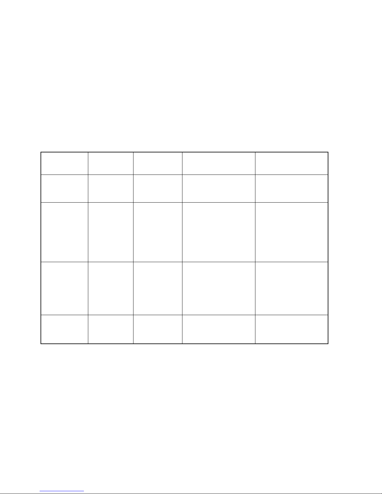
1. DIAGNOSTIC TEST INDICA TORS
When an errors occurs, the STANDBY/TIMER lamp will flash a set number of times to indicate the possible cause of the
problem. If there is more than one error, the lamp will identify the first of the problem areas.
Result for all of the following diagnostic items are displayed on screen. No error has occured if the screen displays a “0”.
Diagnostic
Item
Description
• Power does not
turn on
• +B overcurrent
(OCP) or
overvoltage
(OVP)
• Vertical deflection
stopped
• Horizontal
deflection
overdrive
• White balance
failure (no
PICTURE)
• Micro reset
No. of times
STANDBY/TIMER
lamp flashes
Does not light
2 times
5 times
—
Self-diagnostic
display/Diagnostic
result
—
002:000 or
002:001~255
003:001~255
004:001~255
at the same time
005:000 or
005:001~225
101:00 or
101:001~225
Probable
Cause
Location
• Power cord is not plugged
in.
• Fuse is burned out F4601
(F)
• H.OUT Q511 is shorted. (A
board)
• IC1800 is shorted. (C5
board)
• -13V is not supplied. (A
board)
• IC 503 faulty (A board)
• IC 301 faulty (A board)
• G2 is improperly adjusted.
(Note 2)
• CRT problem.
• Video OUT IC1800 is faulty.
(C5 board)
• IC301 is faulty. (A board)
• No connection A board tox
C5 board.
• Discharge CRT (C5 Board)
• Static discharge
• External noise
Detected
Symptoms
• Power does not come on.
• No power is supplied to the
TV.
• AC power supply is faulty.
• Power does not come on.
• Load on power line is
shorted.
• Has entered standby state
after horizontal raster.
• Vertical deflection pulse is
stopped.
• Power line is shorted or
power supply is stopped.
• No raster is generated.
• CRT cathode current
detection reference pulse
output is small.
• Power is shut down shortly,
after this return back to
normal.
• Detect Micro latch up.
Note 1: If a + B overcurrent is detected, stoppage of the vertical deflection is detected simultaneously.
The symptom that is diagnosed first by the microcontroller is displayed on the screen.
Note 2: Refer to screen (G2) Adjustment in section 3-4 of this manual.
SELF DIAGNOSTIC FUNCTION

– 5 –
KV-XF21M83/XF21M93
RM-952
2. DISPLAY OF STANDBY/TIMER LIGHT FLASH COUNT
Diagnostic Item Flash Count*
+B overcurrent/overvoltage 2 times
Vertical deflection stopped
White balance failure 5 times
* One flash count is not used for self-diagnostic.
3. STOPPING THE STANDBY/TIMER FLASH
Turn off the power switch on the TV main unit or unplug the power cord from the outlet to stop the STANDBY/TIMER lamp
from flashing.
Lamp ON 0.3 sec.
Lamp OFF 3 sec.
Lamp OFF 0.3 sec.
2 times
5 times
STANDBY/SLEEP lamp

– 6 –
KV-XF21M83/XF21M93
RM-952
4. SELF-DIAGNOSTIC SCREEN DISPLAY
For errors with symptoms such as “power sometimes shuts off” or “screen sometimes goes out” that cannot be confirmed, it
is possible to bring up past occurances of failure for confirmation on the screen:
[To Bring Up Screen Test]
In standby mode, press buttons on the remote commander sequentially in rapid succession as shown below:
[Screendisplay] / channel [5] / Sound volume [-] / Power ON
˘
Note that this differs from entering the service mode (mode volume [+]).
Self-Diagnosis screen display
002 : 000
003 : 000
004 : 000
005 : 001
Numeral "0" means that no fault has been detected.
Numeral "1" means a fault has been detected.
101 : 000
SELF DIAGNOSTIC
5. HANDLING OF SELF-DIAGNOSTIC SCREEN DISPLAY
Since the diagnostic results displayed on the screen are not automatically cleared, always check the self-diagnostic screen
during repairs. When you have completed the repairs, clear the result display to “0”.
Unless the result display is cleared to “0”, the self-diagnostic function will not be able to detect subsequent faults after
completion of the repairs.
[Clearing the result display]
To clear the result display to “0”, press buttons on the remote commander sequentially as shown below when the diagnostic
screen is being displayed.
Channel [8] / 0
[Quitting Self-diagnostic screen]
To quit the entire self-diagnostic screen, turn off the power switch on the remote commander or the main unit.
– 7 –
KV-XF21M83/XF21M93
RM-952
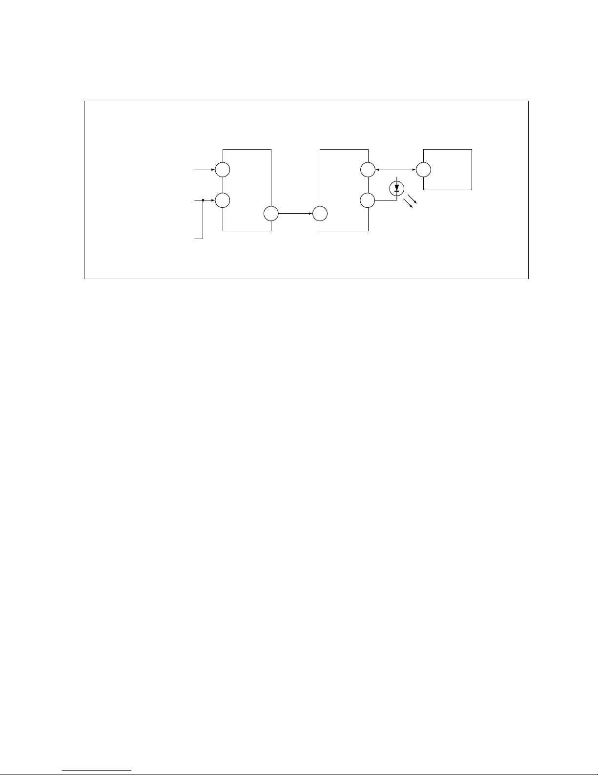
6. SELF-DIAGNOSTIC CIRCUIT
[+BovercurrentªOCPº]
Occurs when an overcurrent on the +B(135) line is detected by Q604. If Q604 go to ON
and the voltage to pin 18 of IC301 should go down when V.SYNC is more than seven
verticals in a period, the unit will automatically turn off.
[Verticaldeflectionstopped] Occurs when an absence of the vertical deflection pulse is detected by Q509 and IC001
shut down the power supply.
[Verticaldeflectionovercurrent] Occurs when an overcurrent on V drive line is detected by Q507. Power supply will be
shut down when detect this by IC001.
[Whitebalancefailure] If the RGB levels* do not balance or become low level within 5 seconds, this error will be
detected by IC301. TV will stay on, but there will be no picture.
* (Refers to the RGB levels of the AKB detection Ref pulse that detects IK.)
IC301
Y/CHROMA JUNGLE
FROM
CRT
FROM
[+B] Q604 C5
[V] Q509/507
IC001
SYSTEM
IC003
MEMORY
B-DAT
IO-SDAT
IK-IN
MP/
PROTECT
IO-8DAT
O-LED
SDA
54521
18 51
4635
– 8 –
KV-XF21M83/XF21M93
RM-952
SECTION 1
GENERAL
The operating instructions mentioned here are partial abstracts
from the Operating Instruction Manual. The page numbers of
the Operating Instruction Manual remain as in the manual.
2
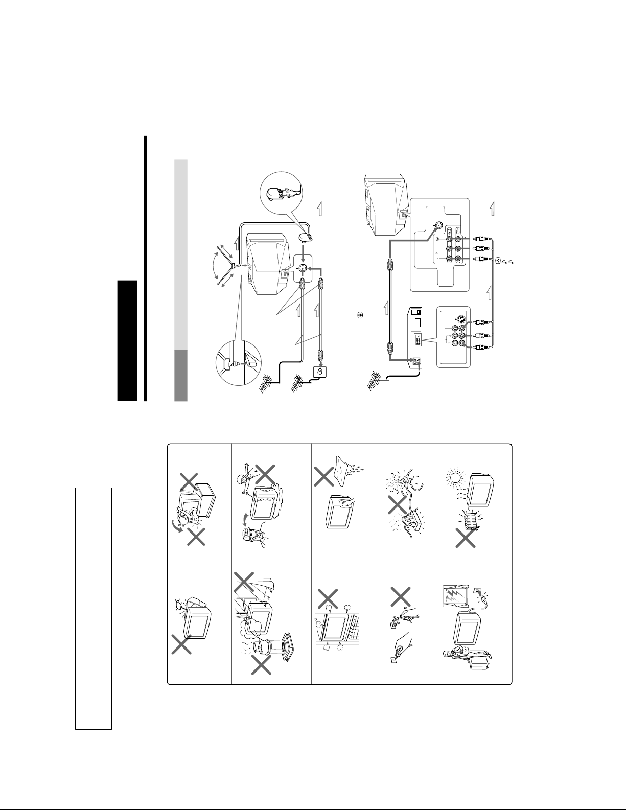
WARNING
• Dangerously high voltages are present inside the TV.
• Operate the TV only between 110 – 240 V AC.
To prevent fire or shock hazard, do not expose
the TV to rain or moisture.
Do not operate the TV if any liquid or solid object
falls into it. Have it checked immediately by
qualified personnel only.
Do not open the cabinet and the rear cover of the
TV. Refer servicing to qualified personnel.
Do not install the TV in hot, humid or excessively
dusty places.
Do not install the TV in a confined space, such
as a bookcase or built-in cabinet.
Do not block the ventilation openings of the TV.
Do not pull the power cord to disconnect the TV.
Pull it out by the plug.
Disconnect the power cord during lightning
storms or if you are not going to use the TV for
several days.
Install the TV in a stable position. Do not allow
children to climb onto it.
Do not plug in too many appliances to the same
power socket. Do not damage the power cord.
Clean the TV with a dry and soft cloth.
Do not use benzine, thinner, or any other chemicals
to clean the TV. Do not scratch the picture tube.
4
Using Your New TV
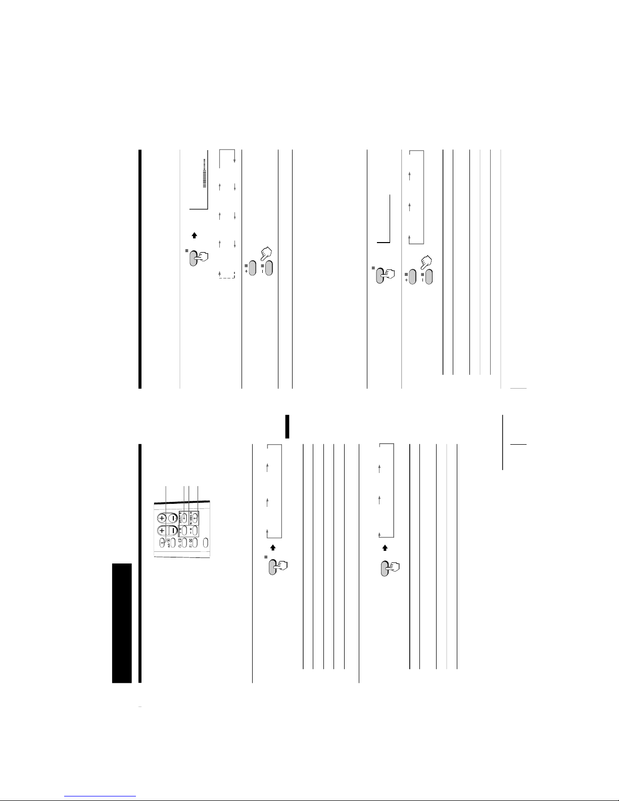
Getting Started
Step 1
Connect the antenna
If you wish to connect a VCR, see the “Connecting a VCR” diagram below.
Using Your New TV
IEC connector
(not supplied)
To video and
audio outputs
VCR
(yellow)
-L (MONO) (white)
-R (red)
Antenna cable (not supplied)
To … 1
(video input)
Audio/Video cable
(not supplied)
: Signal flow
To antenna
output
Antenna cable
(not supplied)
Rear of TV
Rear of TV
Connecting a VCR
To watch the video, press …
(see page 13).
Note
• You are advised to use an outdoor antenna for better reception.
Rod antenna and cable
(not used for these models)
or
VIDEO
VIDEO IN
VIDEO OUT
AUDIO
L(MONO)
1
or
To ˘
(antenna)
: Signal flow
– 9 –
KV-XF21M83/XF21M93
RM-952
5
Using Your New TV
Using Your New TV
Preset the channels automatically
Tips
• If you want to stop automatic channel presetting, press SELECT twice.
• If your TV has preset an unwanted channel or cannot preset a particular
channel, then preset your TV manually (see page 10).
Note
• During automatic channel presetting, your TV screen will indicate “B/G” ,
“I”, “D/K” or “M” for the TV system.
Now You Are Ready. . .
To watch your TV, see page 12.
Notes
• If you connect a monaural VCR, connect the yellow plug to
(the
yellow jack) and the black plug to
-L (MONO) (the white jack).
• If you connect a VCR to the ˘ (antenna) terminal, preset the signal
output from the VCR to the program number 0 on the TV.
• When no signal is input to the connected video equipment, the TV screen
becomes blue.
Step 2
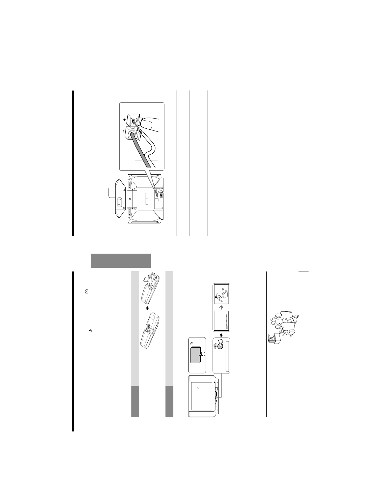
Note
• Do not use old batteries nor use different types of batteries together.
Step 3
CAUTION
Do not connect the power cord until you have completed making all other
connections; otherwise a minimum leakage current might flow through the antenna
and other terminals to ground.
Insert the batteries
into the remote
ONE-PUSH AUTOMATIC PROGRAMING
1
1
ONE-PUSH AUTOMATIC PROGRAMMING
1
2
VHF
LOW
AUTO
Front of TV
6
Using Your New TV
Connecting the 3D WOOFER
You can enjoy high quality sound by connecting the 3D WOOFER.
Rear of TV
WOOFER (8)
L(MONO)
3D WOOFER
Black wire
Red wire
1
2
1
Attach the 3D WOOFER into the footholds on the top of your TV.
2
Connect the wires to the 3D WOOFER (8Ω) terminals at the rear of your TV.
The red wire should be connected to the ‘ red terminal and the black wire
to the ’ black terminal.
Notes
• Connect only the supplied 3D WOOFER; otherwise your TV may
malfunction.
• Unplug your TV from the wall outlet when connecting the 3D WOOFER.
• To prevent a malfunction caused by a short circuit of the terminals, make
sure that none of the 3D WOOFER wire strands stick out, making contact
with the neighbouring speaker terminal.
– 10 –
KV-XF21M83/XF21M93
RM-952
8
Using Your New TV
Securing the TV
To prevent the TV from falling, secure the TV using one of the following methods:
A
With the supplied screws, attach the band to the TV stand and to the rear of
the TV using the provided hole.
or
B
Put the cord or chain through the clamps to secure the TV against a wall or
pillar.
Note
• Use only the supplied screws. Use of other screws may damage the TV.
20
mm
A
B
3.8mm
or
7
Using Your New TV
Using Your New TV
Connecting optional components
You can connect optional audio/video components, such as a VCR, multi disc player,
camcorder, video game or stereo system.
To watch the picture of the connected equipment, press …
(see page 13).
Connecting a camcorder/video game equipment
using the … (video input) jacks
Note
• You can also connect video equipment to the … 1 (video input) jacks at
the rear of your TV.
Connecting audio/video equipment using the Ú
(monitor output) jacks
Note
• When connecting a monaural VCR, connect the yellow plug to
(the
yellow jack) and the black plug to
-L (MONO) (the white jack).
L(MONO)
1
ONE-PUSH AUTOMATIC PROGRAMING
ONE-PUSH AUTOMATIC PROGRAMING
2
Front of TV
Camcorder
Video game
equipment
To video and
audio outputs
(yellow)
-L (MONO)
(white)
-R (red)
Rear of TV
To
antenna
output
To video and
audio inputs
or
Audio system
To
audio
inputs
VCR
:Signal flow
:Signal flow
To
…
2
(video input)
To Ú
(monitor
output)
or
Audio/Video cable (not supplied)
Antenna cable (not supplied)
Audio/Video cable
(not supplied)
or
– 11 –
KV-XF21M83/XF21M93
RM-952
9
Using Your New TV
Using Your New TV
Presetting
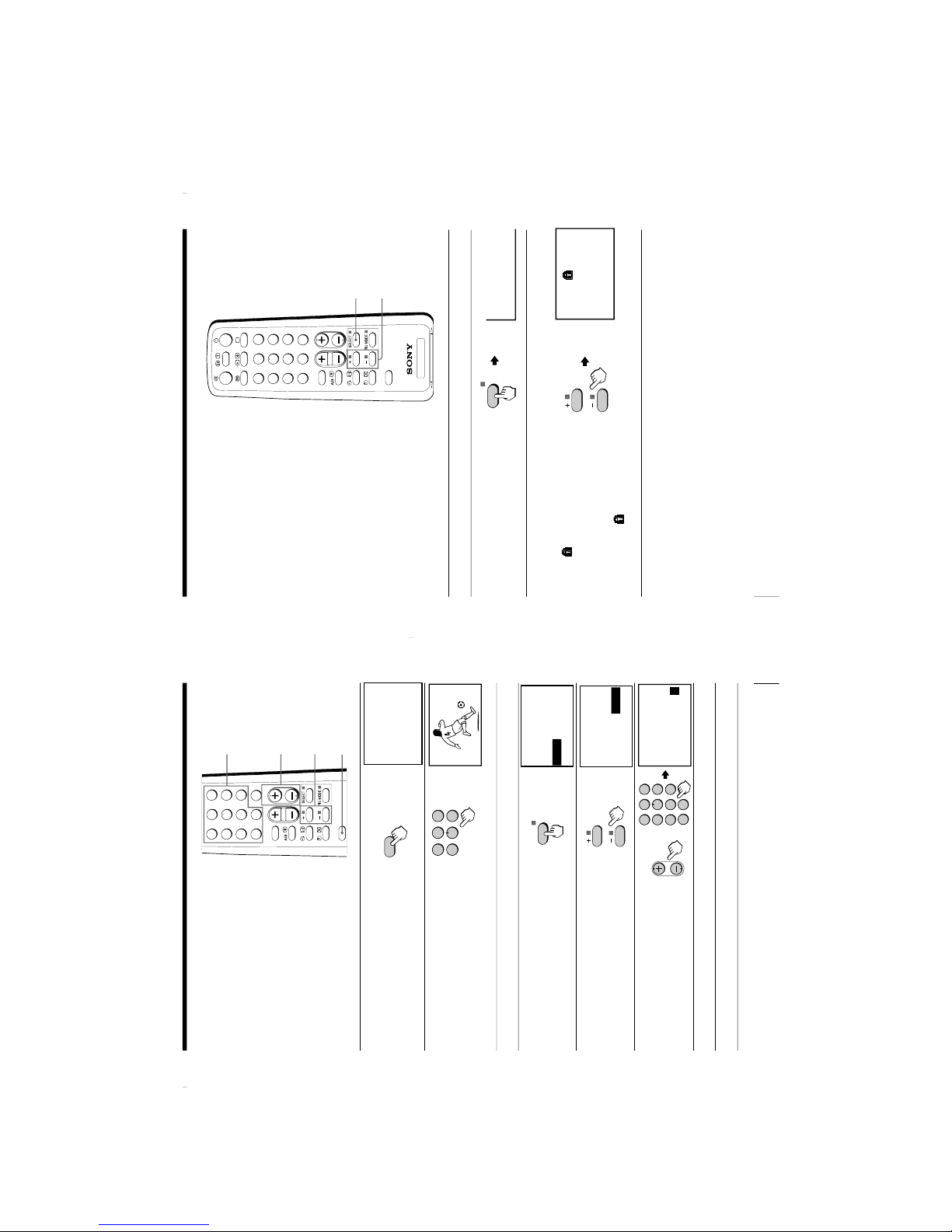
channels
You can preset up to 100 TV channels in
numerical sequence from program
number 1 using the remote and the
buttons on your TV as well.
Presetting channels automatically
1
Press U to turn on the TV.
2
Press AUTO PROGR.
Note (KV-XF21M50 only)
• During automatic channel presetting, your TV screen will indicate “B/G” ,
“I”, “D/K” or “M” for the TV system.
To preset channels automatically from a specified program number
(1) Press SELECT until “AUTO PROGRAM” appears.
(2) Press + or –.
The on-screen display will start flashing.
(3) Press PROGR +/– or the number buttons until the desired program number
appears.
(4) Press + or –.
TV
1
2
346
7
8
9
÷
0
5
JUMP
SOUND
MODE
FAVORITE
PROGRÁ
u
Number buttons
SELECT
. +/–
PROGR +/–
+ or –
PIC MODE
ONE-PUSH AUTOMATIC PROGRAMING
continued
VHF
LOW
AUTO
10
Using Your New TV
Presetting channels (continued)
1
SELECT
b
SELECT
b
or
1
2
3
4
5
6
7
8
0
-/--
9
PROGR
b
Presetting channels manually
1
Press SELECT until
“MANUAL PROGRAM”
appears.
2
Press + or –.
3
Press PROGR +/– or the
number buttons until the
desired program number
appears.4Press + or – until the
desired channel picture
appears.
5
Press SELECT.
To change the TV system setting
If the picture or sound is abnormal when receiving programs through the
˘
(antenna)
terminal
(1) Press SELECT until “TV SYS” appears.
(2) Press + or – to select the appropriate TV system until the picture or sound quality
is optimal.
B/G
I D/K
M
MANUAL PROGRAM
VHF
LOW
B/G
TV SYS: B/G
– 12 –
KV-XF21M83/XF21M93
RM-952
12
Using Your New TV
Watching the TV
This section explains functions used
while watching the TV. Most operations
can be done using the remote.
1
Press U to turn on the TV.
When the TV is in the
standby mode (the u
indicator on the TV is lit
red), press u on the remote
or PROGR +/– on the TV.2Press PROGR +/– or the
number buttons to select
the TV program.
For double digit numbers,
press ÷, then the number
(e.g., for 25, press ÷, then
2 and 5).
3
Press
. +/– to adjust the
volume.
¤
u
…
;
Number buttons
SELECT
. +/–
PROGR +/–
+ or –
TV
1
2
346
7
8
9
÷
0
5
JUMP
SOUND
MODE
FAVORITE
PROGR
SELECT
p
PIC MODE
p
Á
JUMP
FAVORITE
1
2
3
4
5
6
7
8
0
-/--
9
PROGR
or
ONE-PUSH AUTOMATIC PROGRAMING
11
Using Your New TV
Using Your New TV
To change the color system setting
If the color is abnormal when receiving programs through the
˘
(antenna) terminal
or the
…
(video input) jack
(1) Press SELECT until “COL SYS” appears.
(2) Press + or – to select the appropriate color system until the color is optimal.
Tip
• Normally set “COL SYS” to “AUTO”.
Skipping program numbers
1
Press PROGR +/– or the number buttons until the unused or unwanted
program number appears.
2
Press SELECT until “MANUAL PROGRAM” appears.
3
Press + or –.4Press PIC MODE.
5
Press SELECT.
To preset the skipped program number again
Preset the channel automatically or manually.
Tip
• You can also use SELECT and
¸
+/– on the TV to preset channels and
skip program numbers.
To use the fine tuning (FINE) function
The fine tuning (FINE) function may help to reduce the following problems:
incomplete Teletext display (KV-XF21M61/XF21M65 only), double images and lines
moving across the TV screen.
You can use the fine tuning function as below:
(1) Select the program number you want to adjust.
(2) Press SELECT until “MANUAL PROGRAM” appears on the screen.
(3) Press + or – on the remote control once.
(4) Press
to display “FINE” on the screen.
(5) Press + or – continuously until the above problems are minimized.
The + or – icon on the screen flashes while tuning.
(6) Press SELECT to return to normal screen.
AUTO
PAL SECAM
NTSC 3.58 NTSC 4.43
COL SYS: AUTO

– 13 –
KV-XF21M83/XF21M93
RM-952
12
Using Your New TV
To
Turn off temporarily
Turn off completely
Mute the sound
Watch the video input
(VCR, camcorder, etc.)
Jump back to the previous channel
Display the on-screen information*
Adjust the volume of each TV
program automatically
Adjust the picture position when it
is not aligned to the TV screen
Do this
Press u. The u indicator on the TV lights up red.
Press U on the TV.
Press ¤.
Press …
to select “VIDEO 1” or “VIDEO 2”.
To return to the TV program, press ;.
Press JUMP.
Press
.
Press SELECT repeatedly until “INTELLIGENT VOL”
appears, then press + or – to select “ON”.
To cancel, select “OFF”.
Press SELECT repeatedly until “PIC ROTATION”
appears, then press + or – to adjust the alignment of the
picture position
The
or icon on the screen flashes while
adjusting.
* The picture, sound, and either the program number or video mode are
displayed. The on-screen display for the picture and sound information
disappears after about 3 seconds.
Changing the on-screen display language
1
Press SELECT until
“LANGUAGE / :
ENGLISH”appears on the
screen.
2
Press + or – to select
“ “.
Tip
• You can also use SELECT and . +/– on the TV to select the on-screen
display language.
Additional tasks
Watching the TV (continued)
LANGUAGE / : ENGLISH
SELECT
LANGUAGE / :
PIC ROTATION
14
Using Your New TV
Setting the Wake Up timer
1
Press
until the
desired period of time
appears.
2
Select the TV program or video mode you want to display when you wake
up.
3
Press u or set the Sleep timer if you want the TV to turn off automatically.
The
indicator on the TV lights up orange.
To cancel the Wake Up timer
Press until “WAKE UP TIMER: OFF” appears or turn off the
TV’s main power.
Notes
• The Wake Up timer starts immediately after the on-screen display
disappears.
• If no buttons or controls are pressed for more than two hours after the
TV is turned on using the Wake Up timer, the TV automatically goes into
the standby mode. To continue watching the TV, press any button or
control on the TV or the remote.
Setting the Sleep timer
Press until the
desired period of time
appears.
To cancel the Sleep timer
Press until “SLEEP TIMER: OFF” appears or turn the TV off.
WAKE UP TIMER:10M
WAKE UP TIMER:OFF
WAKE UP TIMER:12H00M
After 10 minutes
No Wake Up Timer After 12 hours
SLEEP TIMER:30M
SLEEP TIMER:60M
SLEEP TIMER:OFF
SLEEP TIMER:90M
After 30 minutes
No Sleep Timer
After 60 minutes
After 90 minutes
Watching the TV (continued)
– 14 –
KV-XF21M83/XF21M93
RM-952
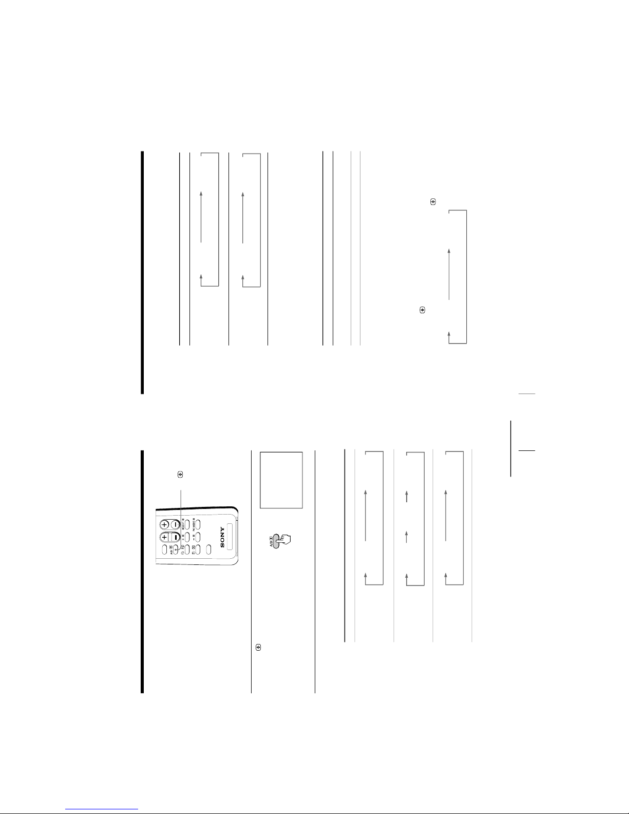
15
Advanced Operations
Advanced Operations
Advanced Operations
SOUND MODE
Customizing the
picture and sound
You can customize the picture and
sound by selecting the picture and
sound modes or by adjusting its
settings.
You can change the sound effect by
selecting the surround mode.
Selecting the picture and sound modes
To select the picture mode
Press PIC MODE
repeatedly until you get
the desired picture mode.
Select To
DYNAMIC receive high contrast pictures.
STANDARD receive normal contrast pictures.
SOFT receive mild pictures.
To select the sound mode
Press SOUND MODE
repeatedly until you get
the desired sound mode.
Select To
DYNAMIC listen to dynamic and clear sound that emphasizes the low and
high sound.
DRAMA listen to sound that emphasizes vocals and background music.
SOFT receive soft sound.
PIC MODE
SELECT
+ or –
≥
DYNAMIC
≥
DRAMA
≥
SOFT
SOUND
MODE
STANDARDDYNAMIC SOFT
PIC MODE
continued
SOUND
MODE
FAVORITE
PROGRÁ
16
Advanced Operations
Adjusting the picture and sound settings
1
Press SELECT until the
desired setting appears.
Each time you press
SELECT, the setting
item will change as follows:
2
Press + or – to adjust the
item.
3
To adjust other items, repeat steps 1 to 2.
* “HUE” can be adjusted for the NTSC system only.
Notes
• When you select a picture or sound mode, the adjusted settings will be
reset according to the selected mode.
• You can also use SELECT and
¸
+/– on the TV to adjust the picture and
sound settings.
Selecting the surround mode
1
Press SELECT repeatedly
until “SURROUND”
appears.
2
Press + or – to select the
desired surround sound.
Select To
MOVIE listen to sound that spreads out over a large area, giving the feeling
of being at a movie theatre.
MUSIC listen to the sound that gives the feeling of being at a live concert.
OFF turn off the surround sound.
MUSICMOVIE
OFF
SURROUND: MOVIE
Customizing the picture and sound (continued)
b
SELECT
b
SELECT
PICTURE 60
PICTURE COLOR
BRIGHT HUE*
BALANCE TREBLE
BASS
SHARP
– 15 –
KV-XF21M83/XF21M93
RM-952
17
Advanced Operations
Advanced Operations
Viewing your
favorite channels
You can display six of your favorite
channels for quick and easy selection.
You can change the favorite channel
setting as well.
Selecting a favorite channel
1
Press FAVORITE.2Press the number button
from 1 to 6 to select the
desired channel.
When you use the FAVORITE CH
feature for the first time, six preset channels will appear.
1
2
346
7
8
9
÷
0
5
JUMP
SOUND
MODE
FAVORITE
PROGRÁ
FAVORITE
+ or –
PROGR +/–
Number
buttons
1
FAVORITE CH
1PR01 2PR02 3PR03
4PR04 5PR05 6PR06
FAVORITE CH SET UP
1PR01 2PR02 3PR03
4PR04 5PR05 6PR06
1PR01 2PR02 3PR03
4PR04 5PR05 6PR06
FAVORITE CH SET UP
Changing the favorite channel setting
1
Press SELECT until
“FAVORITE CH SET UP”
appears.
2
Press + or – to select the
favorite channel you want
to change (e.g. 3 PR03).3Press PROGR +/–, or
number buttons to
change the program
number.
4
Repeat steps 2 and 3 to set other favorite channels.
5
Press SELECT.
b
FAVORITE
1
2
3
4
5
6
b
SELECT
b
b
1
2
3
4
5
6
7
8
0
-/--
9
PR01
PR02PR08
PR04 PR05 PR06
123
456
FAVORITE CH SET UP
PROGR
or
18
Advanced Operations
Blocking the
channels
(CHILD LOCK)
You can prevent a child from watching
certain programs by using the buttons
on the remote control.
1
Select the TV program you want to lock.
2
Press SELECT until “CHILD
LOCK” appears on the
screen.
3
Press + or – to select
“ON”.
The
symbol appears on
the screen.
To unlock the channel,
press + or – to select
“OFF”. The
symbol
disappears from the screen.
Note
• If you preset a locked channel, that particular channel will be unlocked
automatically.
CHILD LOCK: ON
1
CHILD LOCK: OFF
SELECT
TV
1
2
346
7
8
9
÷
0
5
JUMP
SOUND
MODE
FAVORITE
PROGRÁ
SELECT
+ or –
– 16 –
KV-XF21M83/XF21M93
RM-952
19
Advanced Operations
Advanced Operations
TV
SOUND
MODE
FAVORITE
PROGRÁ
Broadcasting On-screen display (Selected sound)
NICAM stereo
NICAM bilingual
NICAM monaural
Selecting a stereo
or bilingual
program
(KV-XF21M93 only)
You can enjoy stereo sound or bilingual
programs of NICAM and A2 (German)
stereo systems.
Press A/B
repeatedly
until you receive the
sound you want.
The on-screen display changes
to show the selected sound
and the  indicator on the TV
lights up red.
When receiving a NICAM program
b
STEREO
NICAM
MONO
(Stereo sound)
(Regular sound)
NICAM
MAIN
MONO
(Main sound)
(Regular sound)
NICAM
SUB
(Sub sound)
NICAM
MAIN
MONO
(Main sound)
(Regular sound)
continued
A/B
20
Advanced Operations
When receiving an A2 (German) program
Notes
• If the signal is very weak, the sound becomes monaural automatically.
• If the stereo sound is noisy when receiving a NICAM program, select
“MONO”. The sound becomes monaural, but the noise is reduced.
Receiving area for NICAM and A2 (German) programs
• Before receiving a NICAM stereo program in China, please check the
NICAM broadcast condition at your area. When receiving a NICAM
stereo program, the receiving condition might vary depending on area. In
addition, different strength of the NICAM broadcast signal might affect
the receiving quality.
If the sound is distorted or noisy when receiving a monaural
program through the ˘ (antenna) terminal
Press A/B repeatedly until “MONO” appears on the screen.
To cancel the monaural sound setting, press A/B
again until
“AUTO” appears on the screen.
Notes
• The “MONO” or “AUTO” setting is memorized for each program
position.
• You cannot receive stereo broadcast signal when the TV is in the “MONO”
setting. Normally set the TV to “AUTO.”
Broadcasting On-screen display (Selected sound)
A2 (German) stereo
A2 (German) bilingual
System
NICAM
A2 (German)
Receiving area
Hong Kong, Singapore, New Zealand, Malaysia,
Thailand, etc.
Australia, Malaysia, Thailand, etc.
STEREO
MONO
(Stereo sound)
(Regular sound)
MONO
AUTO
Selecting a stereo or bilingual program (continued)
MAIN
SUB
(Main sound)
(Sub sound)
 Loading...