

Page 1
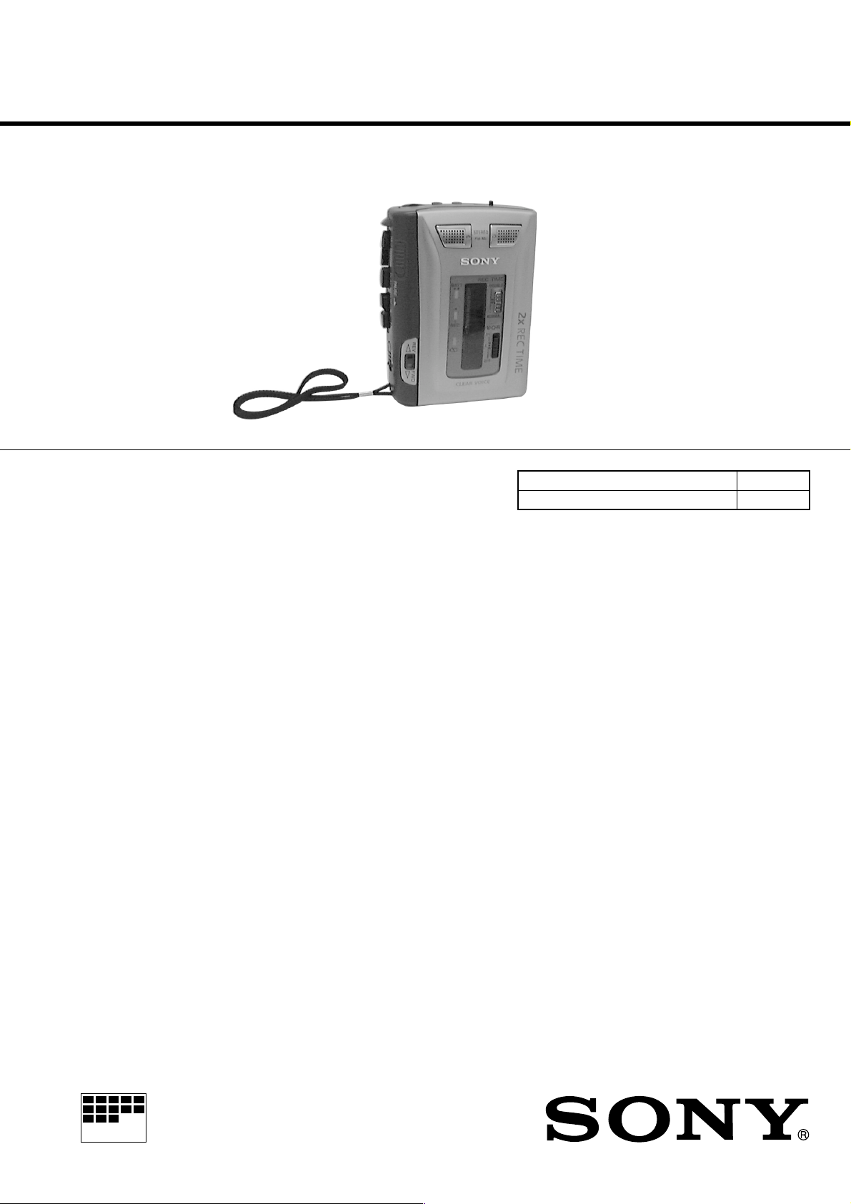
TCS-60DV
SERVICE MANUAL
Ver 1.1 2000. 11
With SUPPLEMENT-1 (9-926-969-81)
SPECIFICATIONS
US Model
Canadian Model
AEP Model
E Model
Model Name Using Similar Mechanism TCM-50DV
Tape Transport Mechanism Type MT-50-30
Recording system 4-track 2 channel stereo
Tape speed 4.8 cm/s or 2.4 cm/s
Frequency range 250 – 8,000 Hz using nomal (TYPE1) cassette
(with REC TIME switch at “NORMAL”)
Speaker Approx. 3.6 cm (17/16 in.) dia. ×2
Power output Speakers : 160 mW + 160 mW
(at 10 % harmonic distortion)
Headphones : 6 mW + 6 mW
(at 10 % harmonic distortion)
Input Microphone input jack (minijack) sensitivity
0.2 mV for 3 Ω or lower impedance
microphone
Output 2 (headphones) jack (minijack) for
8 – 300 Ω earphone
Variable range of the tape speed
From approx. +25 % to – 15 %
(with REC TIME switch at “NOMAL”)
Power requirements 3 V DC batteries AA (R6) ×2/
External DC 3 V power sources
Dimensions (w/h/d)(incl. projecting parts and controls)
Approx. 88.7 × 113.4 × 41.3 mm
(31/2 × 41/2 × 111/16 inches), incl.
Mass Approx. 280 g (9.9 oz)
Design and specifications are subject to change without notice
MICROFILM
CASSETTE CORDER
Page 2

TABLE OF CONTENTS
1. SERVICE NOTE·······························································3
2. GENERAL ·········································································· 4
3. DISASSEMBLY
3-1. Cabinet (rear) Assy, Lid Sub Assy, Cassette··················· 5
3-2. MAIN Board, Mechanism Deck ····································· 5
3-3. Belt·················································································· 6
3-4. Head ················································································ 6
3-5. Motor, DC ······································································· 7
3-6. Precaution For Attaching The MAIN Board··················· 7
4. ADJUSTMENT ································································· 8
5. DIAGRAMS
5-1. Block Diagram ································································ 9
5-2. Schematic Diagram······················································· 11
5-3. Printed Wiring Board –MAIN Section – ······················15
5-4. Printed Wiring Board –LED Section – ·························20
5-5. IC Block Diagrams ······················································· 24
5-6. IC Pin Function Discription ·········································· 26
6. EXPLODED VIEWS
6-1. MAIN Section -1 ··························································27
6-2. MAIN Section -2 ··························································28
6-3. Mechanism Deck Section -1 ········································· 29
6-4. Mechanism Deck Section -2 ········································· 30
7. ELECTRICAL PARTS LIST ······································· 31
Notes on chip component replacement
• Never reuse a disconnected chip component.
• Notice that the minus side of a tantalum capacitor may be
damaged by heat.
Flexible Circuit Board Repairing
• Keep the temperature of soldering iron around 270˚C
during repairing.
• Do not touch the soldering iron on the same conductor of the
circuit board (within 3 times).
• Be careful not to apply force on the conductor when soldering
or unsoldering.
— 2 —
Page 3
SECTION 1
SERVICE NOTE
The TCS-60DV detects rotation of both the supply and take-up side
reels using the PH701 (photo reflector). Because the PH701 is
mounted on the Main board, auto stop is activated and reel rotation
cannot be detected when the Main board is removed. To check the
operation of mechanism deck and voltage without the Main board,
follow the procedure as described below.
How to remove the Main board (opening the Main board)
1) Refer to page 5 “3. Disassembly”.
How to enter the fast forward/rewind modes
1) Input the square wave to the TP41. (Refer to the illustration
below.)
2) Press the fast forward/rewind keys.
3) Turn on the S301.
How to enter the playback mode
1) Input the square wave to the TP41. (Refer to the illustration
below.)
2) Press the playback key.
3) Set the S302 to the PLAY.
4) Turn on the S301.
How to enter the record mode
1) Input the square wave to the TP41. (Refer to the illustration
below.)
2) Press the record key.
3) Set the S302 to the REC.
4) Turn on the S301.
Oscillator
PULSE
10Hz 1.6V (4.5dB)
TP1
(Side B) (Side A)(Side A)
TP41
S301
S302
— 3 —
Page 4
SECTION 2
GENERAL
This section is extracted
from instruction manual.
1 2 Headphone jack
2 MIC (PULG IN POWER) jack
3 VOL knob
4 r REC button
5 p STOP button
6 PLAY button
7 SPEED CONTROL knob
8 REW/REVIEW button
9 FF/CUE button
0 DIR c switch
!¡ Hand strap
!™ Tape direction indicators
!£ SPEAKER (REAR SIDE)
!¢ TAPE COUNTER switch
!∞ Flat mic
!§ PAUSE c switch
!¶ REC TIME switch
!• BATT/REC indicator
!ª VOR switch
@º Battery compartment
@¡ i indicator
@™ DC IN 3V jack
— 4 —
Page 5

Disassemble the unit in the order as shown below.
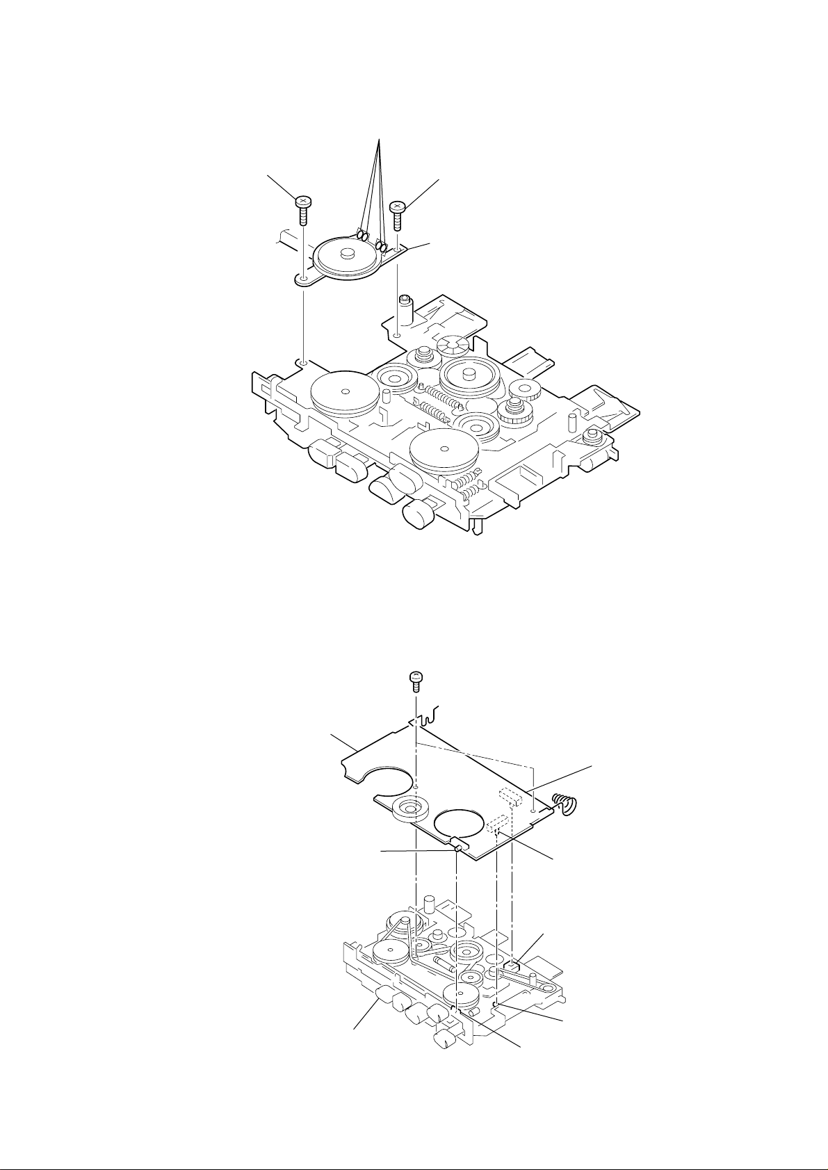
SECTION 3
DISASSEMBLY
Set "Cabinet (rear) assy", "lid sub assy, cassette" Main board, Mechanism deck Belt
Note : Follow the disassembly procedure in the numerical order given.
3-1. “CABINET (REAR) ASSY”, “LID SUB ASSY, CASSETTE”
9
Lid Sub Assy, Cassette
5
PWB, LED Flexible
8
Screw, ornamental
Claws
7
Screw, ornamental
6
Shaft(A), stopper
3
Remove the Cabinet (rear) assy
in the direction of the allow
4
Remove speaker cable (4pcs)
Claws
Head
Motor, dc
2
Two screws(+B1.7 × 9)
3-2. MAIN BOARD, MECHANISM DECK
NOTE: For attaching the Main board,
refer to the next page.
1
Three screws(IB LOCK)
2
4
1
Two screws(+B1.7 × 9)
8
Mechanism deck
6
PC board, Head flexible
3
— 5 —
5
PC board, Motor flexible
7
MAIN board
Two screws(M1.4), Toothed lock
Page 6
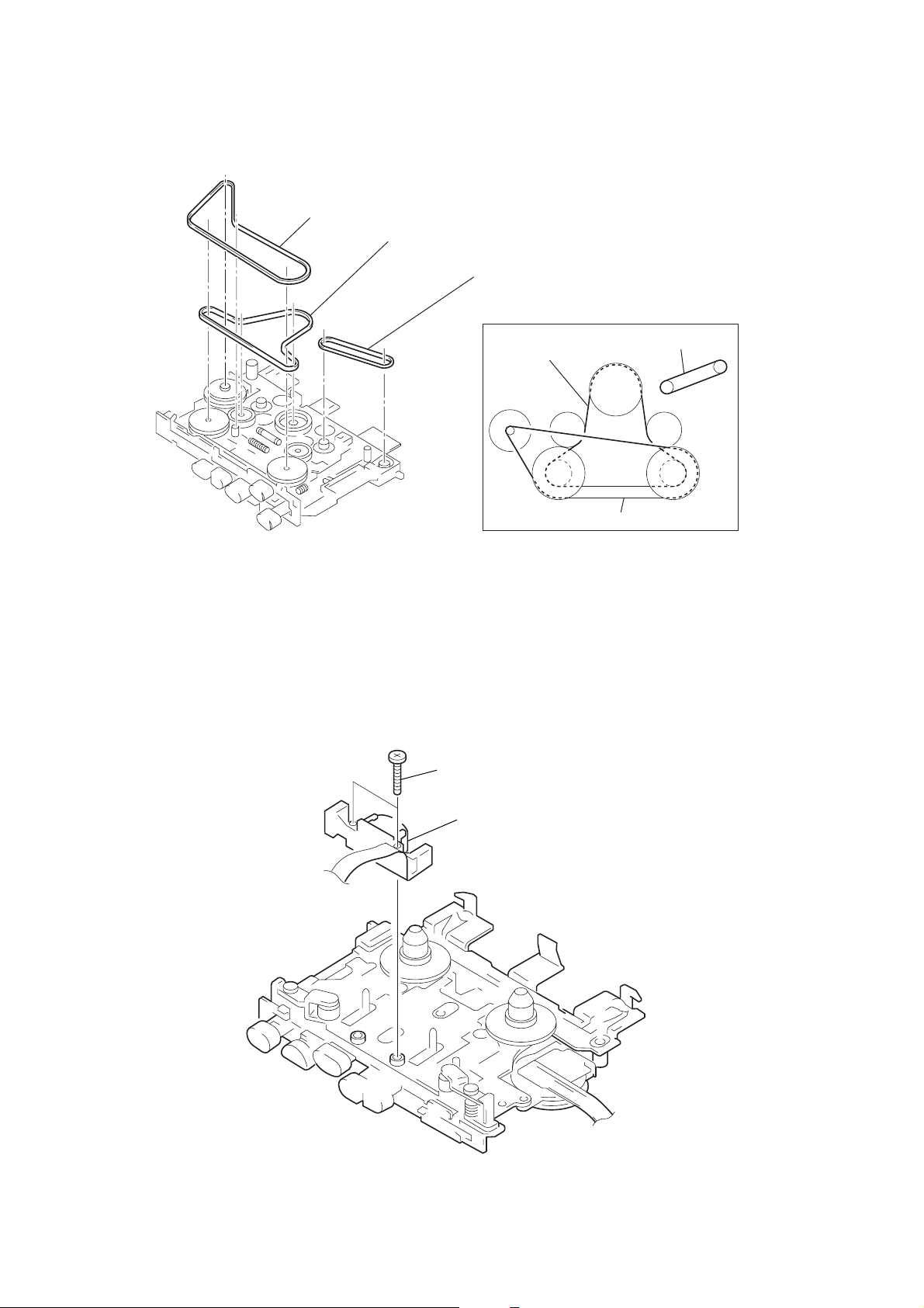
3-3. BELT
1
Belt(motor)
2
Belt(flywheel)
3
Belt(counter)
• How to thread the belt
Belt(flywheel)
Belt(motor)
Belt(counter)
3-4. HEAD
1
two screws
2
head, magnetic
(REC/PB/ERASE)
— 6 —
Page 7
3-5. MOTOR, DC
)
3 Remove the four solders.
2 screw (1.4)
1 screw (1.4)
4 Motor, DC
3-6. PRECAUTION FOR ATTACHING THE MAIN BOARD
• Attach the knobs of the switches S302, S303, and S701 on the Main board
while aligning them with the claws of the REC lever, write-protection 2
lever, and the PAUSE lever respectively.
MAIN board
S701
S303
S302
Write-protection lever
(align it with S303)
Mechanism deck
REC lever
(align it with S302)
PAUSE lever (align it with S701
— 7 —— 7 —
Page 8
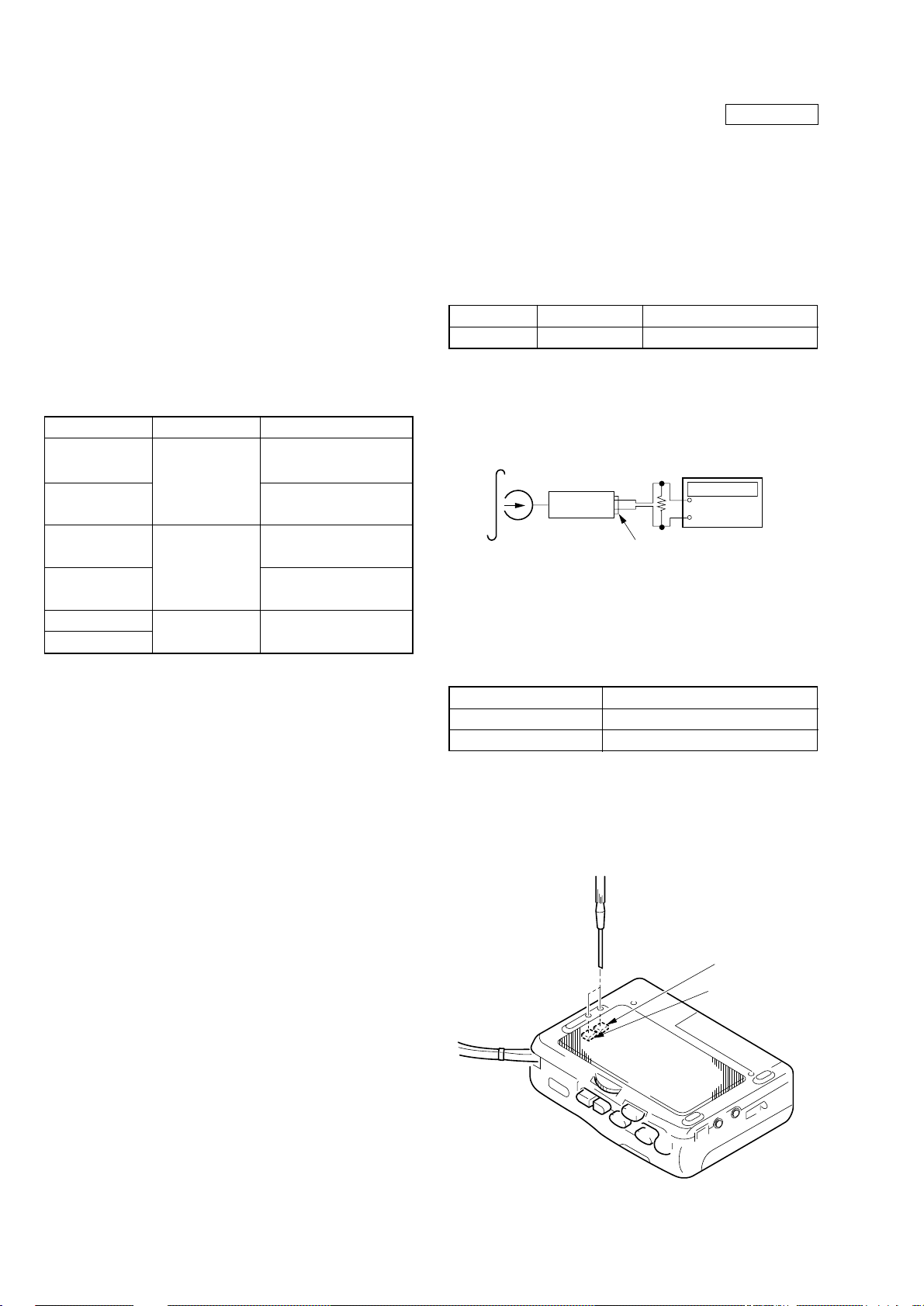
SECTION 4
y
)
ADJUSTMENTS
4-1. MECHANICAL ADJUSTMENT
PRECAUTION
1. Clean the following parts with a denatured-alchool-moistened
swab:
record/playback/erase head pinch roller
head rubber belts
capstans idlers
2. Demagnetize the record/playback/erase head with a head
demagnetizer. (Do not bring the head demagnetizer close to
the erase head.)
3. Do not use a magnetized screwdriver for the adjustments.
4. After the adjustments, apply suitable locking compound to the
parts adjusted.
5. Unless specified otherwise, use a specified voltage (3.0V) to
perform the adjustments.
Torque Measurement
Mode
FWD
FWD
back tension
FWD
FWD
back tension
FF
REW
Torque Meter
CQ-102C
CQ-102RC
CQ-201B
Meter Reading
20 – 35g•cm
0.28 – 0.48 oz•inch
0.5 – 5.0g•cm
0.007 – 0.07 oz•inch
20 – 35g•cm
0.28 – 0.48 oz•inch
0.5 – 5.0g•cm
0.007 – 0.07 oz•inch
more than 40g•cm
more than 0.5 oz•inch
4-2. ELECTRICAL ADJUSTMENT
0dB = 0.775V
1. Perform adjustments on the following conditions unless
otherwise specified.
• Switches and controls positions
VOL knob···························································· Maximum
SPEED CONTROL knob ······················· Mechanical center
V•O•R switch ································································OFF
REC TIME switch ····················································Normal
Test tape
Test Tape
WS-48A
Signal
3kHz, 0dB
Tape speed adjustment
Used for
Tape Speed Adjustment
Procedure :
Mode : Playback (FWD)
test tape
WS-48A
(3kHz, 0dB)
set
Headphone jack(J303)
digital frequenc
counter
16
Ω
+
–
Adjust R V602 (standard)/R V603 (double speed) until the frequency
counter reading
becomes 3,000 Hz at the standard mode and 1,500 Hz at the double
speed mode.
Specification Value :
Tape speed
RV602(Normal)
RV603(High)
Digital frequency counter
2,970 – 3,030Hz
1,485 – 1,515Hz
Frequency difference between the beginning and the end of the
tape should be within 1% (30Hz).
Upon completion of adjustments, select the REV playback mode
and check that the measurement value is within the specifications.
Adjustment Location :
RV603(HIGH)
RV602(NORMAL
— 8 —— 8 —
Page 9
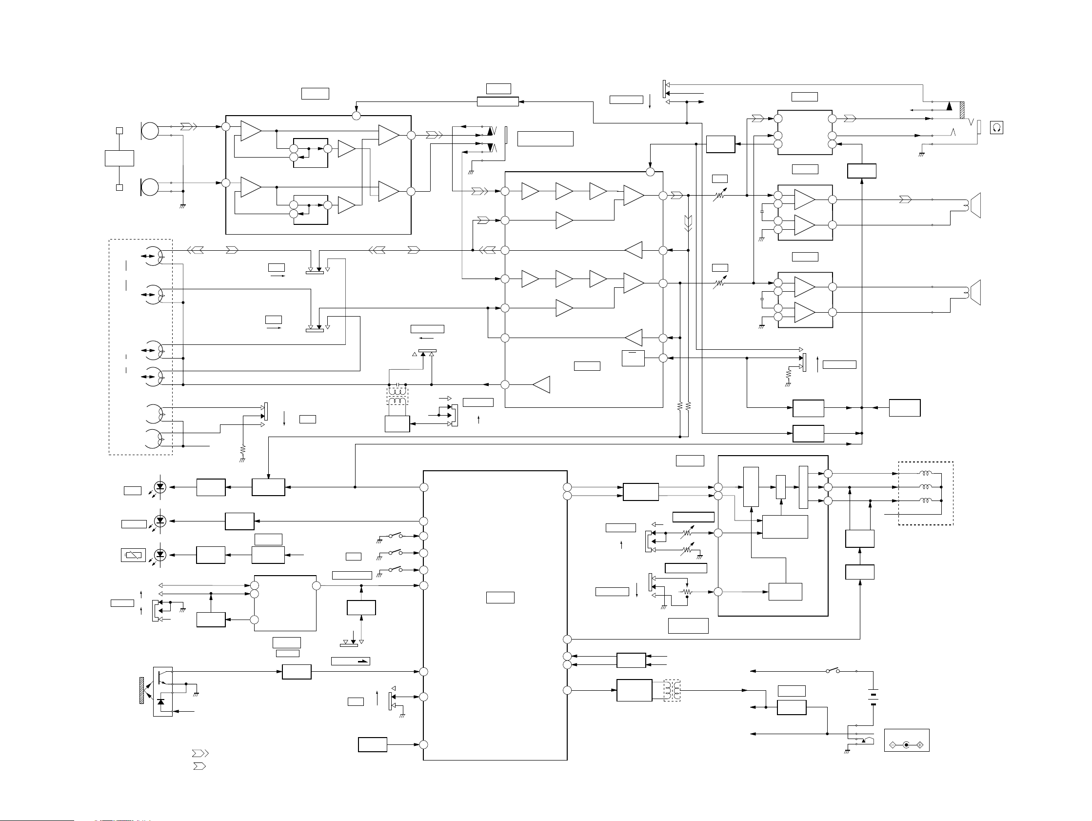
5-1. BLOCK DIAGRAM
MIC901
L
STEREO
Flat Mic
MIC902
R
HRPE901
L CH
FWD
R CH
L CH
REV
R CH
ERASE
(FWD)
ERASE
(REV)
S501
..
V O R
16
<
>
<
>
D502
REC
D501
POWER
D503
OFF
LOW
HIGH
PH701
(TAPE END DET.)
SIGNAL PATH
PLAY:
REC:
Q504
LED
SWITCH
Q505
LED
SWITCH
SWITCH
Q501
B+
6
24
REC B+
+
–
+
–
Q703
LED
SWITCH
SECTION 5
DIAGRAMS
S303(1/4)
DIR
FWD
S303(2/4)
DIR
FWD
FWD
REV
VOICE
MIRROR
Q502,503
IC502
BATTERY
DETECT
5
RCV TIME
1
IN
6 OUT 2
IC501
V O R
9
8
21
23
REV
REV
S303(3/4)
OUT 1
..
SWITCH
Q708
IC301
MIC AMP
DIR
B+
7
10
20
PAUSE
7
Vcc
S702
(FWD/RCV)
S703
DIR
S704
REW/FF
SWITCH
B+
S701
S303(4/4)
DIR
Q705,706
T301
Q301
REV
FWD
RESET
+
–
+
–
Q701
BIAS
OSC
13
17
S302(2/4)
REC/PLAY
REC
REC B+
18
OUT-4
17
OUT-5
IN-2
5
6
IN-3
IN-5
8
4
IN-1
10 IN-7
11 IN-8
CL
3
PLAY
IC303
REGULATOR
2
3
23
22
15
1
S601(1/2)
REC TIME
NORMAL
HIGH
IC701
SYSTEM CONTROL
J301
MIC
(PLUG IN POWER)
MIC
MIC
GCA
PB
GCA
PB
REF
OUT-2
OUT-1
IN-4
IN-6
CONT
IC305
REC/PLAY
PRE AMP
20
21
19OUT-3
7
9
23
AMP
AMP
REC TIME
S302(4/4)
REC/PLAY
S302(1/4)
REC/PLAY
LINE
+
–
LINE
+
–
CONTROL
S601(2/2)
NORMAL
HIGH
Q707
SWITCH
D-D CONV.
REC
REC
PB/
REC
Q704
MOTOR
PLAY
REC
Q702
OSC
PLAY
REC
14
Vcc
8
910
17
16
13
IC601
MOTOR SERVO
RV602
TAPE SPEED
RV603
TAPE SPEED
RV601
SPEED
CONTROL
B+
REC B+
T701
B+
REC B+
Q302
RIPPLE
FILTER
RV301(1/2)
VOL
RV301(2/2)
VOL
19
11
12
13
B+
SYSCON B+
(FOR IC701)
MOTOR SERVO B+
(FOR IC601,M601)
1
16
12 BASE
7
8
5
6
7
8
5
6
DETECT
WAVE FORM
REF.VOLTAGE
CURRENT
DETECT
IC304
HEADPHONE AMP
IN (L)
OUT (L)
OUT (R)
IN (R)
MUTE
IC101
SPEAKER AMP
+
–
–
+
IC201
SPEAKER AMP
+
–
–
+
REC
PLAY
Q307
MUTE
SWITCH
Q308
MUTE
SWITCH
LOGIC
PRE DRIVER
(POWER)
IC702
REG
7
10
5
1
3
1
3
S302(3/4)
REC/PLAY
20
1
2
S301
SPEAKER AMP B+
(FOR IC101,201)
Q303
MUTE
B+
MOTOR
Q601,602
BRAKE
Q603,604
SWITCH
+
(
Q304,306
MUTE
SWITCH
(CAPSTAN/REEL MOTOR)
IEC DESIGNATION R6P
M601
U
V
W
DRY BATTERY
SIZE "AA"
2PCS. 3V
J302
DC IN 3V
TCS-60DV
J303
SP901
(SPEAKER L)
SP902
(SPEAKER R)
)
— 9 — — 10 —
Page 10
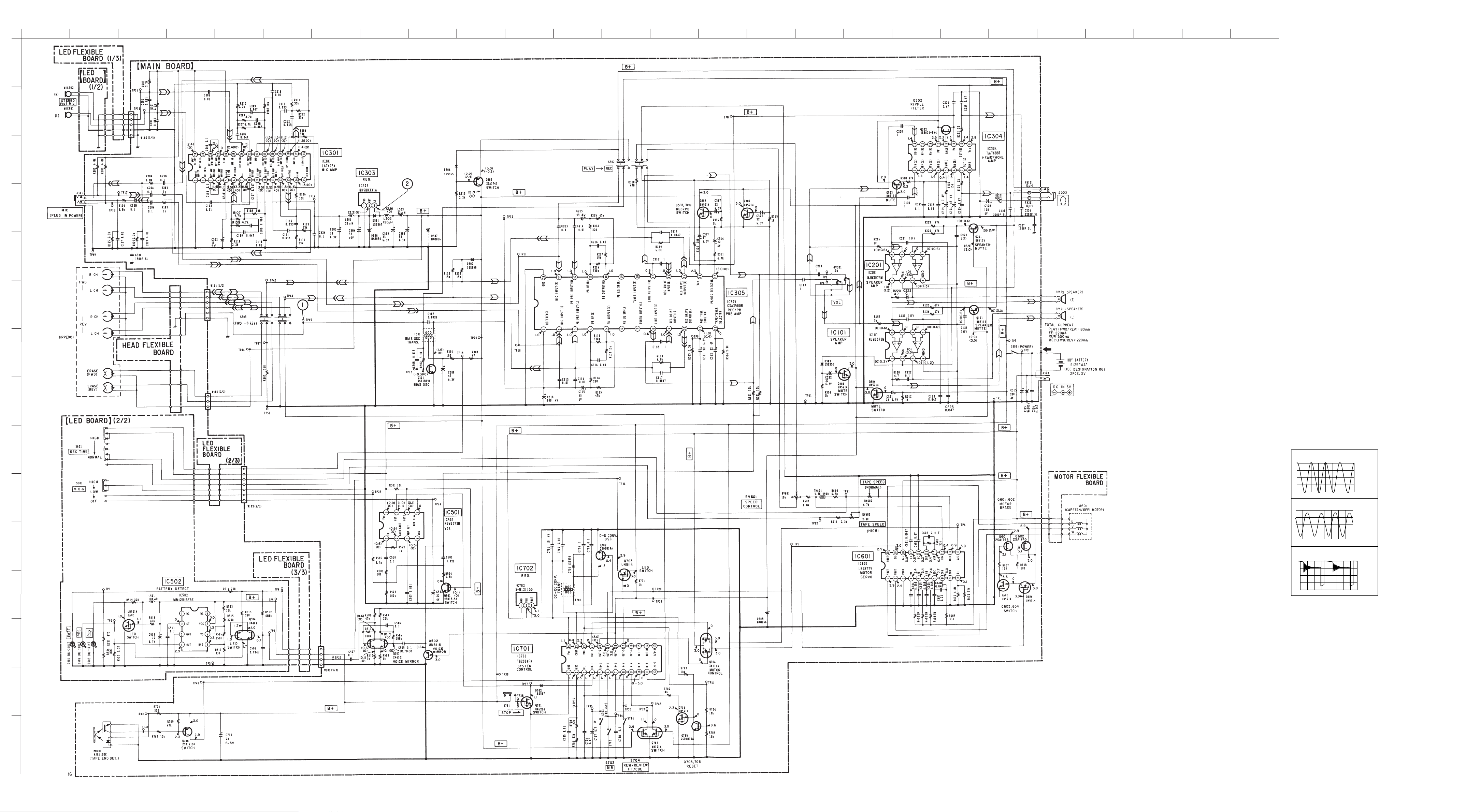
TCS-60DV
5-2. SCHEMATIC DIAGRAM
12
A
B
C
D
34567891011121314151617181920212223242526
E
F
G
H
I
• Wavef orm
TP45 REC DOUBLE MODE
1
10 µsec/div
5 V/div
K
L
M
O
P
J
1
2
Note on Schematic Diagram:
• All capacitors are in µF unless otherwise noted. pF: µµF
50 WV or less are not indicated except for electrolytics
and tantalums.
• All resistors are in Ω and 1/
specified.
• % : indicates tolerance.
• C : panel designation.
• U : B+ Line.
• H : adjustment for repair.
• Power voltage is dc3 V and fed with regulated dc power
supply from battery terminal.
• Voltages and waveforms are dc with respect to ground
under no-signal (detuned) conditions.
no mark : REC/PB
( ) : REC
< > : PB
• Voltages are tak en with a V OM (Input impedance 10 MΩ).
Voltage variations may be noted due to normal production tolerances.
• Waveforms are taken with a oscilloscope.
Voltage variations may be noted due to normal production tolerances.
• Circled numbers refer to waveforms.
• Signal path.
E : REC
a : PB
52 kHz
TP45 REC NORMAL MODE
10 µsec/div
10 V/div
52 kHz
IC303 3 LX REC
5 µsec/div
1 V/div
4
W or less unless otherwise
— 11 — — 12 — — 13 — — 14 —
Page 11

5-3. PRINTED WIRING BOARD – MAIN SECTION –
12
A
B
TCS-60DV
• Semiconductor
3456789101112131415161718192021222324
Location
Ref. No. Location
D301 B-2
D302 B-20
D303 C-23
D304 C-22
D305 E-13
D306 C-20
D307 B-3
D308 C-9
D701 B-9
D702 B-14
IC101 A-5
IC201 B-17
IC301 D-6
IC303 B-3
IC304 B-19
IC305 D-18
IC501 A-15
IC601 E-14
IC701 C-14
IC702 B-15
C
D
E
F
Q101 C-6
Q201 B-6
Q301 D-4
Q302 A-19
Q303 B-18
Q304 C-3
Q305 C-2
Q306 B-2
Q307 D-22
Q308 A-1
Q501 B-15
Q502 C-6
Q503 B-7
Q601 D-11
Q602 E-11
Q603 D-11
Q604 C-11
Q701 B-15
Q702 B-9
Q703 D-15
Q704 C-15
Q705 B-13
Q706 B-13
Q707 D-14
Q708 B-7
G
Note on Printed Wiring Board:
• X : parts extracted from the component side.
• Y : parts extracted from the conductor side.
• Through hole is omit.
• b : Pattern from the side which enables seeing.
Caution:
Pattern face side: Parts on the pattern face side seen from
(SIDE A) the pattern face are indicated.
Parts face side: Parts on the par ts face side seen from
(SIDE B) the parts face are indicated.
— 15 — — 16 — — 17 — — 18 — — 19 —
Page 12

TCS-60DV
5-4. PRINTED WIRING BOARD – LED SECTION –
12
• Semiconductor
345678910111213
Location
Ref. No. Location
D501 E-3
D502 E-4
D503 E-6
A
B
C
IC502 E-5
Q504 E-3
Q505 E-7
D
E
Note on Printed Wiring Board:
• X : parts extracted from the component side.
• Y : parts extracted from the conductor side.
• Through hole is omit.
• b : Pattern from the side which enables seeing.
Caution:
Pattern face side: Parts on the pat tern face side seen from
(SIDE A) the pattern face are indicated.
Parts face side: Parts on the parts face side seen from
(SIDE B) the parts face are indicated.
— 20 — — 21 — — 22 — — 23 — — 24 —
Page 13

5-5. IC BLOCK DIAGRAMS
IC501 NJM2072M IC502 MM1251BFBE
VCC
+
–
CT
INPUT
GAIN CONT
AMP OUT
GND
N.C
1
2
3
4
8
7
6
5
VCC
OUTPUT2
OUTPUT1
RECOVERY
TIME CAP
1 2 3 4
N.C
IC304 T A7688F-S0 IC305 CXA2500N-T4
VS
–
+
BOOSTER
SIRCUIT
GND
HYS
5678
OUT
NF1
VB1
IN1
–
+
MUTE
+
–
1 52 3 4 6 7 8
IN2
NF2
PW
DC
PW-OFF
DC
BY2
VB2
BASE
RIPPLE
FILTER
MUTE
VR
BY1
10111213141516
OUT1
OUT2
REC DRIVE OUTPUT (B)
VCC
PB/REC SELECTOR13
14
15
PB/
REC
NORM/
METAL
TAPE/
TUNER
101112
AGC TIME CONSTANT
REC DRIVE OUTPUT (A)
TAPE/TUNER SELECTOR
PB
PB
PB
GCA
GCA
AGC
AGC
PB OUTPUT (B)
TUNER INPUT(B)
PB EQ SWITCH (B)
20
18
19
AMP
AMP
AMP
5
6
7
PB OUTPUT (A)
TUNER INPUT (A)
PB EQ SWITCH (A)
REC DRIVE INPUT (B)
LINE OUTPUT (B)
16
17
LINE REC
LINE REC
-0.3dB
LINE REC
20.5dB
8
9
LINE OUTPUT (A)
REC DRIVE INPUT (A)
AGC
AGC
DET
DET
PB NF (B)
PB PRE INPUT (B)
MIC INPUT (B)
GND
21
22
23
VCC
9
GND
24
REF
1
REFERENCE
2
MIC INPUT (A)
MIC
MIC
MIC GCA
6dB 22dB 12dB
3
4
PB NF (A)
PB PRE INPUT (A)
Page 14

IC301 LA7473V-TLM
EXT AMP NFB2-R
EXT AMP NFB1-R
EXT IN-R
INPUT SELECT CTL-2
EXT MIC
AMP R
EXT MIC
DET
MIC
VCC
MIC VCC
HPF ON
INT IN-R
INT AMP NFB-R
GND
INT MIC
AMP R
INT AMP OUT-R
MIX BUFF IN-L
MIX
AMP R
192021222324252627282930
MIX AMP OUT-R
OFF
HPF IN-R
ON
EXT
INT
OUTPUT
AMP R
OUT-R
EXT/INT
161718
IC601 LB1877V-TLM
VREF
BIASREF V
BIAS
OUT-L
BIAS
S/S
EXT MIC
AMP L
RIPPLE
FILTER
1 2 3 4 5 6 7 8 9 10 11 12 13 14 15
EXT IN-L
EXT AMP NFB1-L
INPUT SELECT CTL-1
UOUT
20 19 18 17 16 15 14 13 12 11
DRIVER
RIPPLE FILTER
EXT AMP NFB2-L
VCC
INT IN-L
INT AMP NFB-L
DR
STARTUP
DIR LOGIC
OSC
INT MIC
AMP L
VCC
LOCKING
PROTECT
STARTUP
DET
INT AMP OUT-L
LB
MIX BUFF IN-R
FC
TSD
WAVEFORM
DET
MIX
AMP L
OFF
MIX AMP OUT-L
OUT
ON
HPF IN-L
+
–
EXT
INT
VSP
IN+
SPEED
DET
CURRENT
DET
OUTPUT
AMP L
MIC MONO
1 2 3 4 5 6 7 8 9 10
VB
UB
VOUT
WOUT
P-GND
WB
OSC
COM
GND
— 25 —
RI
Page 15

5-6. IC PIN FUNCTION DESCRIPTION
IC701 TB2004FN-020-ER(SYSTEM CONTROL)/MAIN BOARD
Pin No.
1
2
3
4
5
6
7
8
9
10
11
12
13
14 – 16
17
18
19
20
21
22
23
24
Pin Name
GND
OSC
CL
IN-1
IN-2
IN-3
IN-4
IN-5
IN-6
IN-7
IN-8
I/O-1
I/O-2
OUT-8 – 6
OUT-5
OUT-4
OUT-3
OUT-2
OUT-1
VDD
CONT
VCC
I/O
–
Ground
–
For generation of system clock (fosc = 3.2 kHz)
I
Reset signal input
I
PAUSE ON/OFF by the PAUSE switch and V•O•R switch “L”: ON, “OPEN”: OFF
I
Recovery to FWD when opening/closing the cassette lid “L”: ON, “OPEN”: OFF
I
Direction “L”: ON, “OPEN”: OFF
I
REC/PB selection “L”: ON, “OPEN”: OFF
I
FF/REW “L”: ON, “OPEN”: OFF
I
POWER : ON/OFF “L”: ON, “OPEN”: OFF
I
Photo reflector pulse input for tape end detection
I
FWD/REV selection “L”: ON, “OPEN”: OFF
–
Not used
–
Not used
–
Not used
O
LED ON/OFF “L”: ON, “OPEN”: OFF
O
Audio mute “L”: ON, “OPEN”: OFF
O
Motor brake “L”: ON, “OPEN”: OFF
O
Motor direction “L”: FWD, “OPEN”: OFF
O
Motor ON/OFF “L”: ON, “OPEN”: OFF
–
Power supply for CMOS block
O
Voltage doubler circuit control output
–
Power supply for bipolar block
Description
— 26 —
Page 16

NOTE:
1
2
2
3
4
7
11
8
9
5
6
MIC901
MIC902
14
10
12
13
12
A
A
B
B
• -XX, -X mean standardized parts, so they may
have some differences from the original one.
• Items marked “*” are not stocked since they
are seldom required for routine service. Some
delay should be anticipated when ordering these
items.
6-1. MAIN SECTION-1
SECTION 6
EXPLODED VIEWS
• The mechanical parts with no reference number
in the exploded views are not supplied.
• Accessories and packing materials are given in
the last of this parts list.
Ref. No. Part No. Description Remarks Ref. No. Part No. Description Remarks
1 A-3050-908-A LID SUB ASSY, CASSETTE
2 3-704-197-31 SCREW(M1.4 × 3.0), LOCKING
3 3-033-592-01 HOLDER, MICROPHONE
4 3-033-593-01 CUSHION, MICROPHONE
5 3-033-594-01 COVER, MICROPHONE
6 3-318-382-31 SCREW(1.7 × 3), TAPPING
7 1-673-130-11 PWB,LED FLEXIBLE
* 8 3-033-584-01 HOLDER, CASSETTE
9 3-318-382-01 SCREW(1.7 × 3), TAPPING
10 3-311-772-11 SHAFT (A), STOPPER
11 A-3021-186-A LED BOARD, COMPLETE
12 3-315-989-11 SCREW, ORNAMENTAL
13 3-704-245-42 SCREW (1.4)
* 14 X-3370-480-1 TOGGLE ASSY
MIC901 1-542-298-11 MICROPHONE, ELECTRET CONDENSER (L)
MIC902 1-542-298-11 MICROPHONE, ELECTRET CONDENSER (R)
— 27 —
Page 17

6-2. MAIN SECTION-2
51
52
55
53
54
MT-50-30
62
58
56
61
57
59
72
64
SP901
70
65
64
not supplied
67
SP902
68
63
70
69
66
60
71
Ref. No. Part No. Description Remarks Ref. No. Part No. Description Remarks
51 3-704-197-33 SCREW (IB LOCK)
52 X-3377-632-1 CABINET (FRONT) ASSY
53 3-032-431-01 KNOB(PAUSE)
54 3-032-432-01 KNOB(DIR)
55 3-925-231-01 REFLECTOR
56 X-3376-766-1 LEVER ASSY,COVERING INDICATION
57 3-831-441-99 SPACER, KNOB
58 3-925-230-01 SPRING, BATTERY COIL
59 3-925-229-01 TERMINAL, PLUS
60 4-017-441-01 CUSHION (B)
61 3-345-648-01 SCREW (M1.4), TOOTHED LOCK
62 A-3021-185-A MAIN BOARD, COMPLETE
63 X-3377-552-1 CABINET (REAR) ASSY
64 3-318-382-31 SCREW (1.7 × 3), TAPPING
65 3-328-319-01 STRAP, HAND
66 3-032-441-01 SHEET (PICK)
67 9-911-815-01 CUSHION
68 3-033-582-01 LID, BATTERY CASE
69 3-032-436-01 FOOT(B), RUBBER
70 3-318-203-92 SCREW (B1.7 × 9), TAPPING
* 71 3-035-577-01 PAPER, SHIELD
72 3-570-611-00 SHEET, PROTECTION, LID
SP901 1-544-657-11 SPEAKER (3.6cm) (L)
SP902 1-544-657-11 SPEAKER (3.6cm) (R)
— 28 —
Page 18

6-3. MECHANISM DECK SECTION-1
(MT-50-30)
113
107
108
114
111
HRPE901
128
130
129
110
117
116
not
supplied
not
supplied
119
118
127
112
121
129
120
130
122
NOTE : Refer to next page.
112
•
A
not
supplied
128
not supplied
123
104
115
105
M601
109
103
124
102
106
Ref. No. Part No. Description Remarks Ref. No. Part No. Description Remarks
101 3-925-247-11 BUTTON, FF
102 3-925-246-11 BUTTON, REW
103 3-925-245-11 BUTTON, PLAY
104 3-032-787-01 BUTTON, REC
105 3-925-248-11 BUTTON, STOP
106 3-924-595-01 SPRING (PINCH-N), TORSION
107 X-3370-380-1 ARM(PINCH-R) ASSY
108 3-924-596-01 SPRING (PINCH-R), TORSION
109 X-3370-379-1 ARM(PINCH-N) ASSY
* 110 3-924-572-01 LEVER (DIR)
101
126
125
117 X-3370-375-1 TABLE ASSY, REEL
* 118 3-924-535-01 LEVER (FR)
* 119 3-924-534-01 LEVER (C/R)
* 120 3-924-538-01 LEVER (S-OFF)
121 3-321-483-11 RING, RETAINING
122 3-924-569-01 PAD(S-OFF)
123 1-657-172-11 PC BOARD, MOTOR FLEXIBLE
124 3-704-245-42 SCREW (1.4)
125 3-035-367-11 BELT (MOTOR)
126 3-924-577-01 PULLEY (COUNTER)
* 111 3-924-575-01 LEVER (DIR-M)
112 3-924-601-01 SPRING, TENSION
113 X-3370-378-1 LEVER (HEAD) ASSY
114 3-938-133-01 SCREW
115 3-018-121-01 SPRING (B.T), COMPRESSION
116 3-365-630-02 SCREW (M1.4)
* 127 3-924-536-01 LEVER (OFF)
128 3-924-602-01 SPRING, TENSION
129 3-305-925-00 WASHER
130 3-321-483-01 RING, RETAINING
M601 1-698-804-21 MOTOR, DC
(including PULLEY)(CAPSTAN/REEL)
HRPE9011-500-590-11 HEAD, MAGNETIC (REC/PB/ERAES)
— 29 —
Page 19

6-4. MECHANISM DECK SECTION-2
(MT-50-30)
158
156
160
159
158
177
180
154
161
155
163
153
151
(included • A)
NOTE : Refer to befor page
152
191
164
166
167
162
161
168
165
169
159
185
176
175
172
171
174
173
170
159
178
179
159
183
184
183
184
181
159
182
186
187
188
157
189
not supplied
190
Ref. No. Part No. Description Remarks Ref. No. Part No. Description Remarks
151 X-3370-373-1 CHASSIS ASSY
* 152 3-924-537-01 LEVER (F/R)
153 3-924-605-01 SPRING (FF), TENSION
154 3-924-593-01 BELT (FLYWHEEL)
155 3-701-437-51 WASHER
156 X-3377-138-1 FLYWHEEL ASSY
157 3-924-602-01 SPRING, TENSION
158 3-924-558-01 PULLEY (T)
159 3-321-483-11 RING, RETAINING
160 3-924-548-01 ARM(T-N)
161 3-924-557-01 GEAR (T)
162 3-924-549-01 ARM(T-R)
* 163 3-924-539-01 LEVER (REW-F)
* 164 3-924-540-01 LEVER (REW-R)
165 3-924-603-01 SPRING (F/R), TENSION
166 3-924-597-01 SPRING (F/R), TORSION
* 167 3-924-568-01 LEVER (FF)
* 168 3-924-567-01 LEVER (REW)
* 169 3-924-566-01 LEVER (STOP)
* 170 X-3370-377-1 LEVER (REC) ASSY
172 3-924-598-01 SPRING (P/S), TORSION
173 3-924-604-01 SPRING (PLAY), TENSION
* 174 3-924-547-01 ARM (PLAY-SUB)
* 175 3-924-545-01 LEVER (LOCK)
* 176 3-924-546-01 LEVER (SW)
177 3-924-606-01 SPRING (LOCK), TENSION
178 3-924-725-01 REFLECTOR
179 3-924-579-01 GEAR (REF)
180 3-348-993-01 WASHER
181 X-3370-376-1 LEVER (CENTER) ASSY
182 3-924-556-01 GEAR (REW)
183 3-924-562-01 GEAR (FF)
184 3-924-560-01 GEAR (REEL)
185 3-924-600-01 SPRING (REC), TENSION
186 3-032-620-01 BELT (COUNTER)
187 3-704-245-42 SCREW (1.4)
188 3-032-438-01 BRACKET (COUNTER)
189 1-548-582-11 COUNTER, TAPE (SMALL TYPE)
* 190 3-924-574-01 LEVER (PAUSE)
191 3-924-607-01 SPRING (ARM-T), TENSION
* 171 3-924-565-01 LEVER (PLAY)
— 30 —
Page 20

SECTION 7
ELECTRICAL PARTS LIST
NOTE:
• Due to standardization, replacements in the
parts list may be different from the parts
specified in the diagrams or the components
used on the set.
• -XX, -X mean standardized parts, so they
may have some difference from the original
one.
• Items marked “*” are not stocked since they
are seldom required for routine service.
Some delay should be anticipated when
ordering these items.
Ref. No. Part No. Description Remarks Ref. No. Part No. Description Remarks
A-3021-185-A MAIN BOARD, COMPLETE
********************
< CAPACITOR >
C101 1-162-964-11 CERAMIC CHIP 0.001uF 10% 50V
C102 1-162-970-11 CERAMIC CHIP 0.01uF 10% 25V
C104 1-107-826-91 CERAMIC CHIP 0.1uF 10% 16V
C106 1-107-826-91 CERAMIC CHIP 0.1uF 10% 16V
C107 1-165-176-11 CERAMIC CHIP 0.047uF 10% 16V
C108 1-164-490-11 CERAMIC CHIP 0.068uF 16V
C109 1-165-176-11 CERAMIC CHIP 0.047uF 10% 16V
C110 1-162-970-11 CERAMIC CHIP 0.01uF 10% 25V
C111 1-164-677-11 CERAMIC CHIP 0.033uF 10% 16V
C112 1-164-677-11 CERAMIC CHIP 0.033uF 10% 16V
C113 1-162-970-11 CERAMIC CHIP 0.01uF 10% 25V
C114 1-162-970-11 CERAMIC CHIP 0.01uF 10% 25V
C115 1-135-318-11 TANTAL. CHIP 33uF 20% 4V
C116 1-162-970-11 CERAMIC CHIP 0.01uF 10% 25V
C117 1-162-968-11 CERAMIC CHIP 0.0047uF 10% 50V
C118 1-164-346-11 CERAMIC CHIP 1uF 16V
C119 1-164-346-11 CERAMIC CHIP 1uF 16V
C120 1-164-346-11 CERAMIC CHIP 1uF 16V
C121 1-164-346-11 CERAMIC CHIP 1uF 16V
C122 1-107-826-91 CERAMIC CHIP 0.1uF 10% 16V
C123 1-165-176-11 CERAMIC CHIP 0.047uF 10% 16V
C124 1-104-908-11 TANTAL. CHIP 47uF 20% 4V
C125 1-164-005-11 CERAMIC CHIP 0.47uF 25V
C126 1-164-676-11 CERAMIC CHIP 2200PF 5% 16V
C127 1-162-970-11 CERAMIC CHIP 0.01uF 10% 25V
C128 1-107-826-91 CERAMIC CHIP 0.1uF 10% 16V
C129 1-164-346-11 CERAMIC CHIP 1uF 16V
C201 1-162-964-11 CERAMIC CHIP 0.001uF 10% 50V
C202 1-162-970-11 CERAMIC CHIP 0.01uF 10% 25V
C204 1-107-826-91 CERAMIC CHIP 0.1uF 10% 16V
C206 1-107-826-91 CERAMIC CHIP 0.1uF 10% 16V
C207 1-165-176-11 CERAMIC CHIP 0.047uF 10% 16V
C208 1-164-490-11 CERAMIC CHIP 0.068uF 16V
C209 1-165-176-11 CERAMIC CHIP 0.047uF 10% 16V
C210 1-162-970-11 CERAMIC CHIP 0.01uF 10% 25V
C211 1-164-677-11 CERAMIC CHIP 0.033uF 10% 16V
C212 1-164-677-11 CERAMIC CHIP 0.033uF 10% 16V
C213 1-162-970-11 CERAMIC CHIP 0.01uF 10% 25V
C214 1-162-970-11 CERAMIC CHIP 0.01uF 10% 25V
C215 1-135-318-11 TANTAL. CHIP 33uF 20% 4V
• CAPACITORS:
uF: µF
• RESISTORS
All resistors are in ohms.
METAL: metal-film resistor
METAL OXIDE: Metal Oxide-film resistor
F: nonflammable
• COILS
uH: µH
C216 1-162-970-11 CERAMIC CHIP 0.01uF 10% 25V
C217 1-162-968-11 CERAMIC CHIP 0.0047uF 10% 50V
C218 1-164-346-11 CERAMIC CHIP 1uF 16V
C219 1-164-346-11 CERAMIC CHIP 1uF 16V
C220 1-164-346-11 CERAMIC CHIP 1uF 16V
C221 1-164-346-11 CERAMIC CHIP 1uF 16V
C222 1-107-826-91 CERAMIC CHIP 0.1uF 10% 16V
C223 1-165-176-11 CERAMIC CHIP 0.047uF 10% 16V
C224 1-164-005-11 CERAMIC CHIP 0.47uF 25V
C225 1-164-005-11 CERAMIC CHIP 0.47uF 25V
C226 1-164-676-11 CERAMIC CHIP 2200PF 5% 16V
C227 1-162-970-11 CERAMIC CHIP 0.01uF 10% 25V
C228 1-107-826-91 CERAMIC CHIP 0.1uF 10% 16V
C229 1-164-346-11 CERAMIC CHIP 1uF 16V
C302 1-135-201-11 TANTALUM CHIP 10uF 20% 4V
C303 1-135-259-11 TANTAL. CHIP 10uF 20% 6.3V
C304 1-113-682-11 TANTAL. CHIP 33uF 20% 10V
C305 1-104-752-11 TANTAL. CHIP 33uF 20% 6.3V
C306 1-104-752-11 TANTAL. CHIP 33uF 20% 6.3V
C307 1-164-695-11 CERAMIC CHIP 0.0022uF 5% 50V
C308 1-164-245-11 CERAMIC CHIP 0.015uF 10% 25V
C309 1-110-569-11 TANTAL. CHIP 47uF 20% 6.3V
C310 1-104-848-11 TANTAL. CHIP 100uF 20% 4V
C311 1-119-750-11 TANTAL. CHIP 22uF 20% 6.3V
C312 1-104-847-11 TANTAL. CHIP 22uF 20% 4V
C313 1-110-569-11 TANTAL. CHIP 47uF 20% 6.3V
C314 1-104-847-11 TANTAL. CHIP 22uF 20% 4V
C315 1-126-246-11 ELECT CHIP 220uF 20% 4V
C316 1-165-176-11 CERAMIC CHIP 0.047uF 10% 16V
C317 1-119-750-11 TANTAL. CHIP 22uF 20% 6.3V
C318 1-162-970-11 CERAMIC CHIP 0.01uF 10% 25V
C319 1-135-151-21 TANTALUM CHIP 4.7uF 20% 4V
C320 1-104-848-11 TANTAL. CHIP 100uF 20% 4V
C321 1-119-750-11 TANTAL. CHIP 22uF 20% 6.3V
C322 1-119-750-11 TANTAL. CHIP 22uF 20% 6.3V
C323 1-119-750-11 TANTAL. CHIP 22uF 20% 6.3V
C324 1-107-826-91 CERAMIC CHIP 0.1uF 10% 16V
C325 1-107-826-91 CERAMIC CHIP 0.1uF 10% 16V
C326 1-164-672-11 CERAMIC CHIP 1500PF 5% 16V
C327 1-164-672-11 CERAMIC CHIP 1500PF 5% 16V
C501 1-164-227-11 CERAMIC CHIP 0.022uF 10% 25V
C502 1-104-847-11 TANTAL. CHIP 22uF 20% 4V
C503 1-162-964-11 CERAMIC CHIP 0.001uF 10% 50V
C505 1-107-826-91 CERAMIC CHIP 0.1uF 10% 16V
C506 1-107-826-91 CERAMIC CHIP 0.1uF 10% 16V
• SEMICONDUCTORS
In each case, u: µ, for example:
uA...: µA... , uPA... , µPA... ,
uPB... , µPB... , uPC... , µPC... ,
uPD..., µPD...
When indicating parts by reference number,
please include the board name.
MAIN
— 31 —
Page 21

MAIN
Ref. No. Part No. Description Remarks Ref. No. Part No. Description Remarks
C507 1-107-826-91 CERAMIC CHIP 0.1uF 10% 16V
C510 1-107-826-91 CERAMIC CHIP 0.1uF 10% 16V
C601 1-162-968-11 CERAMIC CHIP 0.0047uF 10% 50V
C602 1-164-005-11 CERAMIC CHIP 0.47uF 25V
C603 1-164-337-11 CERAMIC CHIP 2.2uF 16V
L301 1-412-030-11 INDUCTOR CHIP 22uH
L302 1-414-222-11 INDUCTOR 120uH
L303 1-412-030-11 INDUCTOR CHIP 22uH
< COIL >
C604 1-110-563-11 CERAMIC CHIP 0.068uF 10% 16V
C605 1-110-563-11 CERAMIC CHIP 0.068uF 10% 16V
C606 1-110-563-11 CERAMIC CHIP 0.068uF 10% 16V
C607 1-115-340-11 CERAMIC CHIP 0.22uF 10% 25V
C608 1-165-176-11 CERAMIC CHIP 0.047uF 10% 16V
C701 1-135-201-11 TANTALUM CHIP 10uF 20% 4V
C702 1-162-970-11 CERAMIC CHIP 0.01uF 10% 25V
C704 1-164-346-11 CERAMIC CHIP 1uF 16V
C705 1-162-970-11 CERAMIC CHIP 0.01uF 10% 25V
C706 1-164-005-11 CERAMIC CHIP 0.47uF 25V
C707 1-135-151-21 TANTALUM CHIP 4.7uF 20% 4V
C708 1-107-826-91 CERAMIC CHIP 0.1uF 10% 16V
C709 1-107-826-91 CERAMIC CHIP 0.1uF 10% 16V
C710 1-119-750-11 TANTAL. CHIP 22uF 20% 6.3V
< DIODE >
D301 8-719-049-09 DIODE 1SS367-T3SONY
D302 8-719-988-61 DIODE 1SS355TE-17
D303 8-719-988-61 DIODE 1SS355TE-17
D304 8-719-988-61 DIODE 1SS355TE-17
D305 8-719-977-03 DIODE DTZ5.6B
D306 8-719-977-03 DIODE DTZ5.6B
D307 8-719-977-03 DIODE DTZ5.6B
D308 8-719-977-03 DIODE DTZ5.6B
D701 8-719-988-61 DIODE 1SS355TE-17
D702 8-719-049-09 DIODE 1SS367-T3SONY
< FERRITE BEAD >
FB101 1-500-444-11 FERRITE 0uH
FB201 1-500-444-11 FERRITE 0uH
FB301 1-500-444-11 FERRITE 0uH
< IC >
IC101 8-759-701-02 IC NJM2073M
IC201 8-759-701-02 IC NJM2073M
IC301 8-759-380-80 IC LA7473V-TLM
IC303 8-759-434-03 IC RH5RH331A-T1
IC304 8-759-205-43 IC TA7688F-SO
IC305 8-752-089-40 IC CXA2500N-T4
IC501 8-759-701-51 IC NJM2072M
IC601 8-759-566-10 IC LB1877V-TLM
IC701 8-759-494-76 IC TB2004FN-020-ER
IC702 8-759-280-84 IC S-81211SG-QA-T1
< JACK >
J301 1-774-321-31 JACK (SMALL TYPE)(MIC)
J302 1-750-061-11 JACK,DC(POLARITY UNIFIED TYPE)(DC IN 3V)
J303 1-695-514-21 JACK (SMALL TYPE) 1P(HEAD PHONE)
< JUMPER CHIP >
JC101 1-216-295-91 SHORT 0
JC102 1-216-864-11 METAL CHIP 0 5% 1/16W
JC103 1-216-295-91 SHORT 0
JC104 1-216-295-91 SHORT 0
< PHOTO INTERRUPTER >
PH701 8-749-925-05 REFLECTOR NJL5183KA-F20-TE1
< TRANSISTOR >
Q101 8-729-420-53 TRANSISTOR UN5115
Q201 8-729-420-53 TRANSISTOR UN5115
Q301 8-729-230-63 TRANSISTOR 2SC4116-YG
Q302 8-729-141-48 TRANSISTOR 2SB624-BV345
Q303 8-729-420-53 TRANSISTOR UN5115
Q304 8-729-402-93 TRANSISTOR UN5214-TX
Q305 8-729-823-86 TRANSISTOR 2SA1745
Q306 8-729-402-93 TRANSISTOR UN5214-TX
Q307 8-729-402-93 TRANSISTOR UN5214-TX
Q308 8-729-402-93 TRANSISTOR UN5214-TX
Q501 8-729-230-63 TRANSISTOR 2SC4116-YG
Q502 8-729-420-53 TRANSISTOR UN5115
Q503 8-729-402-81 TRANSISTOR XN4501
Q601 8-729-823-86 TRANSISTOR 2SA1745
Q602 8-729-823-86 TRANSISTOR 2SA1745
Q603 8-729-402-93 TRANSISTOR UN5214-TX
Q604 8-729-402-96 TRANSISTOR UN5114
Q701 8-729-402-93 TRANSISTOR UN5214-TX
Q702 8-729-230-63 TRANSISTOR 2SC4116-YG
Q703 8-729-402-96 TRANSISTOR UN5114
Q704 8-729-422-41 TRANSISTOR XN1114
Q705 8-729-230-63 TRANSISTOR 2SC4116-YG
Q706 8-729-402-93 TRANSISTOR UN5214-TX
Q707 8-729-420-16 TRANSISTOR XN1214
Q708 8-729-420-24 TRANSISTOR 2SB1218A-QRS
< RESISTOR >
R101 1-216-825-11 METAL CHIP 2.2K 5% 1/16W
R102 1-216-831-11 METAL CHIP 6.8K 5% 1/16W
R103 1-216-821-11 METAL CHIP 1K 5% 1/16W
R104 1-216-831-11 METAL CHIP 6.8K 5% 1/16W
R105 1-216-821-11 METAL CHIP 1K 5% 1/16W
R106 1-216-839-11 METAL CHIP 33K 5% 1/16W
R107 1-216-829-11 METAL CHIP 4.7K 5% 1/16W
R108 1-216-833-91 RES,CHIP 10K 5% 1/16W
R109 1-216-829-11 METAL CHIP 4.7K 5% 1/16W
R110 1-216-825-11 METAL CHIP 2.2K 5% 1/16W
R111 1-216-839-11 METAL CHIP 33K 5% 1/16W
R112 1-216-839-11 METAL CHIP 33K 5% 1/16W
R113 1-216-835-11 METAL CHIP 15K 5% 1/16W
R114 1-216-813-11 METAL CHIP 220 5% 1/16W
R115 1-216-841-11 METAL CHIP 47K 5% 1/16W
R116 1-216-851-11 METAL CHIP 330K 5% 1/16W
R117 1-216-835-11 METAL CHIP 15K 5% 1/16W
R119 1-216-831-11 METAL CHIP 6.8K 5% 1/16W
R120 1-216-793-11 RES,CHIP 4.7 5% 1/16W
R121 1-216-833-91 RES,CHIP 10K 5% 1/16W
— 32 —
Page 22

MAIN LED
Ref. No. Part No. Description Remarks Ref. No. Part No. Description Remarks
R122 1-216-801-11 METAL CHIP 22 5% 1/16W
R123 1-216-841-11 METAL CHIP 47K 5% 1/16W
R124 1-216-841-11 METAL CHIP 47K 5% 1/16W
R125 1-216-825-11 METAL CHIP 2.2K 5% 1/16W
R201 1-216-825-11 METAL CHIP 2.2K 5% 1/16W
R605 1-216-839-11 METAL CHIP 33K 5% 1/16W
R606 1-216-831-11 METAL CHIP 6.8K 5% 1/16W
R607 1-216-809-11 METAL CHIP 100 5% 1/16W
R608 1-216-809-11 METAL CHIP 100 5% 1/16W
R609 1-216-831-11 METAL CHIP 6.8K 5% 1/16W
R202 1-216-831-11 METAL CHIP 6.8K 5% 1/16W
R203 1-216-821-11 METAL CHIP 1K 5% 1/16W
R204 1-216-831-11 METAL CHIP 6.8K 5% 1/16W
R205 1-216-821-11 METAL CHIP 1K 5% 1/16W
R206 1-216-839-11 METAL CHIP 33K 5% 1/16W
R207 1-216-829-11 METAL CHIP 4.7K 5% 1/16W
R208 1-216-833-91 RES,CHIP 10K 5% 1/16W
R209 1-216-829-11 METAL CHIP 4.7K 5% 1/16W
R210 1-216-825-11 METAL CHIP 2.2K 5% 1/16W
R211 1-216-839-11 METAL CHIP 33K 5% 1/16W
R212 1-216-839-11 METAL CHIP 33K 5% 1/16W
R213 1-216-835-11 METAL CHIP 15K 5% 1/16W
R214 1-216-813-11 METAL CHIP 220 5% 1/16W
R215 1-216-841-11 METAL CHIP 47K 5% 1/16W
R216 1-216-851-11 METAL CHIP 330K 5% 1/16W
R217 1-216-835-11 METAL CHIP 15K 5% 1/16W
R219 1-216-831-11 METAL CHIP 6.8K 5% 1/16W
R220 1-216-793-11 RES,CHIP 4.7 5% 1/16W
R221 1-216-833-91 RES,CHIP 10K 5% 1/16W
R222 1-216-801-11 METAL CHIP 22 5% 1/16W
R223 1-216-841-11 METAL CHIP 47K 5% 1/16W
R224 1-216-841-11 METAL CHIP 47K 5% 1/16W
R225 1-216-825-11 METAL CHIP 2.2K 5% 1/16W
R301 1-216-809-11 METAL CHIP 100 5% 1/16W
R302 1-216-827-11 METAL CHIP 3.3K 5% 1/16W
R610 1-216-831-11 METAL CHIP 6.8K 5% 1/16W
R611 1-216-825-11 METAL CHIP 2.2K 5% 1/16W
R612 1-216-839-11 METAL CHIP 33K 5% 1/16W
R701 1-216-839-11 METAL CHIP 33K 5% 1/16W
R702 1-216-833-91 RES,CHIP 10K 5% 1/16W
R703 1-216-833-91 RES,CHIP 10K 5% 1/16W
R704 1-216-833-91 RES,CHIP 10K 5% 1/16W
R705 1-216-833-91 RES,CHIP 10K 5% 1/16W
R706 1-216-815-11 METAL CHIP 330 5% 1/16W
R707 1-216-833-91 RES,CHIP 10K 5% 1/16W
R708 1-216-833-91 RES,CHIP 10K 5% 1/16W
R709 1-216-841-11 METAL CHIP 47K 5% 1/16W
R711 1-216-821-11 METAL CHIP 1K 5% 1/16W
< VARIABLE RESISTOR >
RV601 1-225-293-11 RES, VAR, CARBON 10K(SPEED CONTROL)
RV602 1-238-663-11 RES, ADJ, CARBON 4.7K
RV603 1-223-584-11 RES, ADJ, CARBON 2.2K
< SWITCH >
S301 1-762-594-41 SWITCH, PUSH (1 KEY)(POWER)
S302 1-692-896-11 SWITCH, SLIDE(PLAY/REC)
S303 1-692-896-11 SWITCH, SLIDE(FWD/REV)
S701 1-572-922-11 SWITCH, SLIDE(STOP)
S702 1-572-688-11 SWITCH, PUSH (1 KEY)(FWD RCV)
R303 1-216-863-11 RES,CHIP 3.3M 5% 1/16W
R304 1-216-825-11 METAL CHIP 2.2K 5% 1/16W
R305 1-216-833-91 RES,CHIP 10K 5% 1/16W
R306 1-216-835-11 METAL CHIP 15K 5% 1/16W
R307 1-216-811-11 METAL CHIP 150 5% 1/16W
R308 1-216-841-11 METAL CHIP 47K 5% 1/16W
R309 1-216-805-11 METAL CHIP 47 5% 1/16W
R310 1-216-817-11 METAL CHIP 470 5% 1/16W
R311 1-216-829-11 METAL CHIP 4.7K 5% 1/16W
R312 1-216-821-11 METAL CHIP 1K 5% 1/16W
R313 1-216-825-11 METAL CHIP 2.2K 5% 1/16W
R314 1-216-821-11 METAL CHIP 1K 5% 1/16W
R315 1-216-821-11 METAL CHIP 1K 5% 1/16W
R316 1-216-821-11 METAL CHIP 1K 5% 1/16W
R501 1-216-833-91 RES,CHIP 10K 5% 1/16W
R502 1-216-809-11 METAL CHIP 100 5% 1/16W
R503 1-216-845-11 METAL CHIP 100K 5% 1/16W
R504 1-216-831-11 METAL CHIP 6.8K 5% 1/16W
R505 1-216-827-11 METAL CHIP 3.3K 5% 1/16W
R506 1-216-845-11 METAL CHIP 100K 5% 1/16W
R507 1-216-837-11 METAL CHIP 22K 5% 1/16W
R508 1-216-841-11 METAL CHIP 47K 5% 1/16W
R509 1-216-821-11 METAL CHIP 1K 5% 1/16W
R510 1-216-821-11 METAL CHIP 1K 5% 1/16W
R511 1-216-845-11 METAL CHIP 100K 5% 1/16W
S703 1-572-288-21 SWITCH, PUSH(DIR)
S704 1-762-594-41 SWITCH, PUSH (1 KEY)(REW/FF)
< TRANSFORMER >
T301 1-433-286-11 TRANSFORMER, BIAS OSCILLATION
T701 1-450-667-11 TRANSFORMER, DC-DC CONVERTER
< THERMISTOR >
TH601 1-810-794-11 THERMISTOR, POSITIVE
< FLAT CABLE >
W101 1-750-336-21 CONNECTOR, FFC/FPC (ZIF) 9P
W102 1-573-925-11 CONNECTOR, FFC/FPC (ZIF) 16P
************************************************************
A-3021-186-A LED BOARD, COMPLETE
******************
1-673-130-11 PWB,LED FLEXIBLE
< CAPACITOR >
C508 1-162-968-11 CERAMIC CHIP 0.0047uF 10% 50V
C509 1-119-750-11 TANTAL. CHIP 22uF 20% 6.3V
C511 1-107-826-91 CERAMIC CHIP 0.1uF 10% 16V
R522 1-216-821-11 METAL CHIP 1K 5% 1/16W
R601 1-216-839-11 METAL CHIP 33K 5% 1/16W
R602 1-216-857-11 METAL CHIP 1M 5% 1/16W
R603 1-216-857-11 METAL CHIP 1M 5% 1/16W
R604 1-216-857-11 METAL CHIP 1M 5% 1/16W
— 33 —
Page 23

TCS-60DV
LED
Ref. No. Part No. Description Remarks Ref. No. Part No. Description Remarks
< DIODE >
D501 8-719-059-96 DIODE SML-210LT-T86(POWER)
D502 8-719-059-96 DIODE SML-210LT-T86(REC)
D503 8-719-057-99 DIODE SML-211YT-T86 (BATT CHECK)
< IC >
IC502 8-759-399-49 IC MM1251BFBE
< COIL >
123 1-657-172-11 PC BOARD, MOTOR FLEXIBLE
189 1-548-582-11 COUNTER, TAPE (SMALL TYPE)
M601 1-698-804-21 MOTOR, DC
SP901 1-504-314-12 SPEAKER (3.6CM) (L)
SP902 1-504-314-12 SPEAKER (3.6CM) (R)
MIC901 1-542-298-11 MICROPHONE, ELECTRET CONDENSER (L)
MIC902 1-542-298-11 MICROPHONE, ELECTRET CONDENSER (R)
MISCELLANEOUS
**************
(including PULLEY)(CAPSTAN/REEL)
L501 1-412-032-11 INDUCTOR CHIP 100uH
< TRANSISTOR >
Q504 8-729-402-84 TRANSISTOR XN4601
Q505 8-729-402-93 TRANSISTOR UN5214-TX
< RESISTOR >
R512 1-216-855-11 METAL CHIP 680K 5% 1/16W
R513 1-216-813-11 METAL CHIP 220 5% 1/16W
R514 1-216-813-11 METAL CHIP 220 5% 1/16W
R515 1-216-849-11 METAL CHIP 220K 5% 1/16W
R516 1-216-847-11 METAL CHIP 150K 5% 1/16W
R517 1-216-839-11 METAL CHIP 33K 5% 1/16W
R518 1-216-841-11 METAL CHIP 47K 5% 1/16W
R519 1-216-813-11 METAL CHIP 220 5% 1/16W
R520 1-216-825-11 METAL CHIP 2.2K 5% 1/16W
R521 1-216-817-11 METAL CHIP 470 5% 1/16W
R523 1-216-837-11 METAL CHIP 22K 5% 1/16W
R524 1-216-809-11 METAL CHIP 100 5% 1/16W
< SWITCH >
S501 1-692-605-31 SWITCH, SLIDE(VOR)
S601 1-571-277-51 SWITCH, SLIDE(REC TIME)
HRPE9011-500-590-11 HEAD, MAGNETIC (REC/PB/ERAES)
************************************************************
ACCESSORIES & PACKING MATERIALS
*******************************
X-2542-167-1 STAND ASSY
3-032-436-01 FOOT(B), RUBBER
3-865-283-11 MANUAL, INSTRUCTION
(ENGLISH/FRENCH)(US/Canadian)
3-865-283-21 MANUAL, INSTRUCTION
(ENGLISH/SPANISH/PORTUGUESE)(AEP/E)
3-865-283-31 MANUAL, INSTRUCTION
(FRENCH/GERMAN/DUTCH)(AEP)
3-865-283-41 MANUAL, INSTRUCTION
(SWEDISH/ITALIAN/FINNISH)(AEP)
8-814-296-90 MICROPHONE, CONDENSER ECM-TC60
8-953-130-90 HEADPHONE MDR-E801/K SET(AEP)
9-926-969-11
Sony Corporation
Personal A&V Products Company
— 34 —
Printed in Japan © 1999.3
99C1684-1
Published by Quality Engineering Dept.
(Shinagawa)
Page 24

SERVICE MANUAL
2000. 11
SUPPLEMENT-1
File this supplement with the Service Manual.
Subject : 1. Change of MAIN board
2. Change of Capstan/Reel Motor
TCS-60DV
US Model
Canadian Model
AEP Model
E Model
(SPM-00037)
This service manual supplement-1 only describes the differences between the new and former boards. For other information, refer to the
provided service manual (9-926-969-ss).
To discriminate between the new and former boards, check the part code of the printed wiring board marked on the board.
– MAIN board (side A) –
MAIN board parts No.
Former type : 1-673-132-11
New type : 1-673-132-12
Page 25

1. Changes to the Board
As the motor is changed, the main board is to be changed from the board with the suffix No.-11 to the board with No.-12.
When only replacing the motor or mian board by a new part, replace the appropriate components on the main board.
(For details, refer to “2. Replacing the Board/Motor” on page 9.)
1-1. Printed Wiring Board (page 17)
FORMER TYPE (Board with the suffix No.-11)
(location : C-F,13-16)
RED
WHT
BLK
NEW TYPE (Board with the suffix No.-12)
ORG
110
20 11
BLK
WHT
ORG
RED
— 2 —
Page 26

: indicates corrected portion.
Page FORMER TYPE (Board with the suffix No.-11) NEW TYPE (Board with the suffix No.-12)
(location : E-G,1-3)
15
(location : E-F,10-12)
16
(location : D-G,21-23)
18
RV301
VOL
— 3 —
Page 27

1-2. Schematic Diagram
Page
(location : B-E, 3-8)
: indicates corrected portion.
FORMER TYPE (Board with the suffix No.-11)
11
MIC
(PLUG IN POWER)
NEW TYPE (Board with the suffix No.-12)
15k 0.22
15k 0.22
0.0068
0.0068
— 4 —
Page 28

: indicates corrected portion.
Page
(location : B-D, 14-16)
FORMER TYPE (Board with the suffix No.-11)
13
PLAY REC
NEW TYPE (Board with the suffix No.-12)
3.0
Q307,Q308
C328
0
Q309
22
REC/PB
+
SWITCH
Q309
R731
UN5214
1k
— 5 —
Page 29

: indicates corrected portion.
Page
(location : E-H, 17-19)
FORMER TYPE (Board with the suffix No.-11)
13
NEW TYPE (Board with the suffix No.-12)
R226
6.8k
6.8k
R126
TP6
VOL
3.3k
3.3k
3.3k
— 6 —
Page 30

: indicates corrected portion.
Page
(location : J-L, 18-22)
FORMER TYPE (Board with the suffix No.-11)
13
SPEED
CONTROL
NEW TYPE (Board with the suffix No.-12)
(NORMAL)
3.3k
5.6k
(HIGH)
C609
0.47
22k
— 7 —
Page 31

1-3. Part List
: indicates corrected portion.
Page FORMER TYPE (Board with the suffix No.-11) NEW TYPE (Board with the suffix No.-12)
120
130
129
M601
29
123
124
125
Ref. No. Part No. Description Remarks
123 1-657-172-11 PC BOARD, MOTOR FLEXIBLE
M601 1-698-804-21 MOTOR, DC (INCLUDING PULLEY)
(CAPSTAN / REEL)
120
130
129
(Delete)
M601
124
125
Part No. Description Remarks
——— ————
1-763-273-11 MOTOR, DC (INCLUDING PULLEY)
(CAPSTAN / REEL)
Ref. No. Part No. Description Remarks
C108 1-165-176-11 CERAMIC CHIP 0.068uF 10% 16V
C109 1-165-176-11 CERAMIC CHIP 0.047uF 10% 16V
C127 1-165-970-11 CERAMIC CHIP 0.01uF 10% 25V
31
32
33
C128 1-107-826-91 CERAMIC CHIP 0.1uF 10% 16V
C208 1-164-490-11 CERAMIC CHIP 0.068uF 10% 16V
C209 1-165-176-11 CERAMIC CHIP 0.047uF 10% 16V
C227 1-162-970-11 CERAMIC CHIP 0.01uF 10% 25V
C228 1-107-826-91 CERAMIC CHIP 0.1uF 10% 16V
C328 ——— ————
C609 ——— ————
Q309 ——— ————
R104 1-216-831-11 METAL CHIP 6.8K 5% 1/16W
R121 1-216-833-11 METAL CHIP 10K 5% 1/16W
R126 ——— ————
R204 1-216-831-11 METAL CHIP 6.8K 5% 1/16W
R221 1-216-833-11 METAL CHIP 10K 5% 1/16W
R226 ——— ————
R601 1-216-839-11 METAL CHIP 33K 5% 1/16W
R609 1-216-831-11 METAL CHIP 6.8K 5% 1/16W
R610 1-216-831-11 METAL CHIP 6.8K 5% 1/16W
R731 ——— ————
Part No. Description Remarks
1-162-964-11 CERAMIC CHIP 0.001uF 10% 50V
1-162-970-11 CERAMIC CHIP 0.01uF 10% 25V
1-162-969-11 CERAMIC CHIP 0.0068uF 10% 25V
1-115-467-11 CERAMIC CHIP 0.22uF 10% 10V
1-162-964-11 CERAMIC CHIP 0.001uF 10% 50V
1-162-970-11 CERAMIC CHIP 0.01uF 10% 25V
1-162-969-11 CERAMIC CHIP 0.0068uF 10% 25V
1-115-467-11 CERAMIC CHIP 0.22uF 10% 10V
1-119-750-11 TANTAL. CHIP 22uF 20% 6.3V
1-107-823-11 CERAMIC CHIP 0.47uF 10% 16V
8-729-402-93 TRANSISTOR UN5214-TX
1-216-835-11 METAL CHIP 15K 5% 1/16W
1-216-827-11 METAL CHIP 3.3K 5% 1/16W
1-216-831-11 METAL CHIP 6.8K 5% 1/16W
1-216-835-11 METAL CHIP 15K 5% 1/16W
1-216-827-11 METAL CHIP 3.3K 5% 1/16W
1-216-831-11 METAL CHIP 6.8K 5% 1/16W
1-216-837-11 METAL CHIP 22K 5% 1/16W
1-216-830-11 METAL CHIP 5.6K 5% 1/16W
1-216-827-11 METAL CHIP 3.3K 5% 1/16W
1-216-821-11 METAL CHIP 1K 5% 1/16W
— 8 —
Page 32

2. Replacing the Board/Motor
When riplacing the board or motor only, the following parts are required:
2-1. Replacing the board (when replacing the board with the suffix No.-11 by that with -12 without changing the motor:)
Page BEFORE CHANGE AFTER CHANGE
Ref. No. Part No. Description Remarks
Part No. Description Remarks
32
33
C609 1-107-823-11 CERAMIC CHIP 0.47uF 10% 16V
R601 1-216-837-11 METAL CHIP 22K 5% 1/16W
R610 1-216-827-11 METAL CHIP 3.3K 5% 1/16W
——— ————
1-216-839-11 METAL CHIP 33K 5% 1/16W
1-216-831-11 METAL CHIP 6.8K 5% 1/16W
Note: The new board differs from the former board in the location of the land where the motor flexible board is soldered.
Therefore, the board cannot be used as it is. Remove the motor flexible board and connect the terminals with lead wire.
2-2. Replacing the motor (when replacing by the new motor without changing the boatd with suffix No.-11.)
Page BEFORE CHANGE AFTER CHANGE
Ref. No. Part No. Description Remarks
Part No. Description Remarks
32
33
C609 ——— ————
R601 1-216-839-11 METAL CHIP 33K 5% 1/16W
R610 1-216-831-11 METAL CHIP 6.8K 5% 1/16W
1-107-823-11 CERAMIC CHIP 0.47uF 10% 16V
1-216-837-11 METAL CHIP 22K 5% 1/16W
1-216-827-11 METAL CHIP 3.3K 5% 1/16W
Mounting location of C609
Note: When connecting between C609 and R601, take care to prevent contact between lead and pattern.
C609
— 9 —
Page 33

TCS-60DV
9-926-969-81
Sony Corporation
Audio Entertainment Group
— 10 —
Printed in Japan ©2000.11
2000K1665-1
Published by General Engineering Dept.
 Loading...