

Page 1
TCM-20DV/21DV/
22DV/23DV
SERVICE MANUAL
Ver 1.0 2000. 02
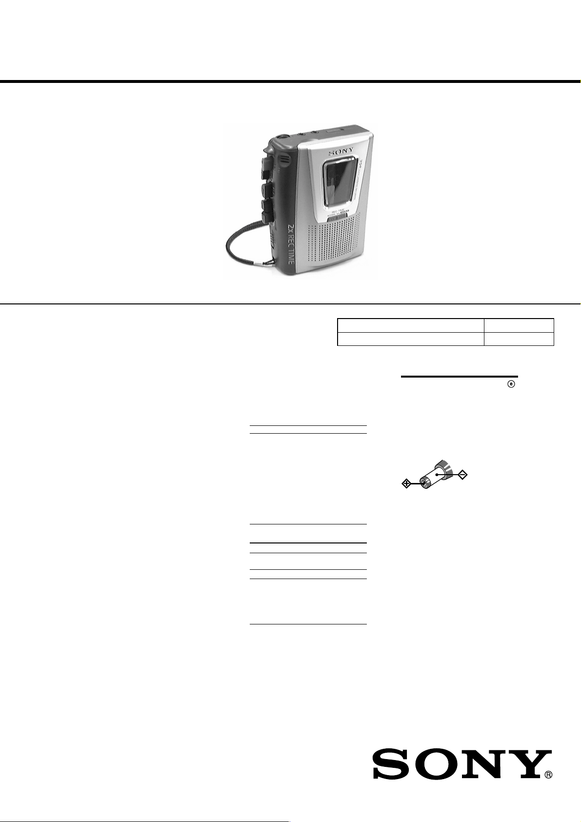
Photo: TCM-20DV
SPECIFICATIONS
Recording system
2-track 1 channel monaural
Tape speed
4.8 cm/s or 2.4 cm/s
Frequency range
250 - 6,300 Hz using nomal (TYPE
I) cassette (with REC TIME switch
at “NORMAL”)
Speaker
Approx. 3.6 cm (1
Power output
250 mW (at 10 % harmonic
distortion)
Input
Microphone input jack (minijack)
sensitivity 0.2 mV for 3 kilohms or
lower impedance microphone
Output
Earphone jack (minijack) for 8 - 300
ohms earphone
Variable range of the tape speed
From approx. +30% to –15% (with
REC TIME switch at “NORMAL”)
Power requirements
3 V DC batteries R6 (AA) × 2/
External DC 3 V power sources
Dimensions (w/h/d) (incl. projecting
parts and controls)
Approx. 112 × 36.6 × 90.3 mm
1
⁄
× 1
(4
2
Mass
Approx. 175 g (6.2 oz.)
1
⁄2 x 3 5⁄8 in.)
7
/16 in.) dia.
Supplied accessories
The instructions in this manual are for
4 models.
The TCM-20DV is the model used for
illustration purposes.
TCM- 23DV 22DV 21DV 20DV
AC power adaptor (1)
Battery charger adaptor (1)
Rechargeable batteries (2)
(NC-AA, 1.2V, 700mAh,
Ni-Cd)
Cassette tape C-90 (1)
Battery LR6 (2)
Monaural microphone (1)
Super-directional
microphone (1)
Carrying pouch (1)
Hand strap (1)
(attached to the unit)
Battery life
Sony alkaline
LR6 (SG)
Sony R6P (SR) 3 3
Sony
rechargeable
battery
(NC-AA) fully
charged (TCM22DV only)
* Measured value by the standard of
EIAJ (Electronic Industries
Association of Japan). (Using a Sony
HF series cassette tape and playing
back with speakers)
Note
The battery life may shorten
depending on the operation of the
unit.
For maximum performance we
recommend that you use alkaline
batteries.
(Approx. hours) (EIAJ*)
Playback Recording
11 11
Model Name Using Similar Mechanism NEW
Tape Transpor t Mechanism Type MT-20DV-118
— a ——
— a ——
— a ——
——a —
——a —
——a —
a ———
——a —
aaaa
33
US Model
TCM-20DV/21DV/22DV/23DV
Canadian Model
TCM-20DV/22DV
AEP Model
TCM-20DV/21DV
E Model
TCM-20DV/23DV
Chinese Model
TCM-20DV
House Current
Connect the AC power adaptor to
DC IN 3V and to a wall outlet. The
AC power adaptor is supplied only
with the TCM-22DV. For other
models, use the AC-E30HG AC
power adaptor (not supplied). Do
not use any other AC power
adaptor.
Note
Specifications for AC-E30HG vary for
each area. Check your local voltage
and the shape of the plug before
purchasing.
Design and specifications are subject
to change without notice.
(see Fig. A- )
Polarity of
the plug
CASSETTE-CORDER
Page 2

SECTION 1
SERVICING NOTES
TABLE OF CONTENTS
1. SERVICING NOTES ............................................... 2
2. GENERAL ................................................................... 3
3. DISASSEMBLY ......................................................... 4
4. MECHANICAL ADJUSTMENTS....................... 7
5. ELECTRICAL ADJUSTMENTS......................... 8
6. DIAGRAMS
6-1. Block Diagram ................................................................ 9
6-2. Printed Wiring Board ...................................................... 11
6-3. Schematic Diagram ......................................................... 13
7. EXPLODED VIEWS ................................................ 16
8. ELECTRICAL PARTS LIST ............................... 19
In this set, the S102 (POWER) detects REC/PLAYBACK on.
It is mounted on the MAIN board, and therefore the REC/PLAYBACK on cannot be detected with the MAIN board removed.
When making an operation check and voltage check of mechanical deck with the MAIN board removed, fix the S102 at turn on.
– MAIN BOARD (Conductor Side) –
S102
on
SAFETY-RELATED COMPONENT WARNING!!
COMPONENTS IDENTIFIED BY MARK 0 OR DOTTED
LINE WITH MARK 0 ON THE SCHEMA TIC DIA GRAMS
AND IN THE PARTS LIST ARE CRITICAL TO SAFE
OPERATION. REPLACE THESE COMPONENTS WITH
SONY PARTS WHOSE PART NUMBERS APPEAR AS
SHOWN IN THIS MANUAL OR IN SUPPLEMENTS PUBLISHED BY SONY.
ATTENTION AU COMPOSANT AYANT RAPPORT
À LA SÉCURITÉ!
LES COMPOSANTS IDENTIFIÉS P AR UNE MARQUE 0
SUR LES DIAGRAMMES SCHÉMATIQUES ET LA LISTE
DES PIÈCES SONT CRITIQUES POUR LA SÉCURITÉ
DE FONCTIONNEMENT. NE REMPLACER CES COMPOSANTS QUE PAR DES PIÈCES SONY DONT LES
NUMÉROS SONT DONNÉS DANS CE MANUEL OU
DANS LES SUPPLÉMENTS PUBLIÉS PAR SONY.
Flexible Circuit Board Repairing
• Keep the temperature of the soldering iron around 270 ˚C during repairing.
• Do not touch the soldering iron on the same conductor of the
circuit board (within 3 times).
• Be careful not to apply force on the conductor when soldering
or unsoldering.
Notes on chip component replacement
• Never reuse a disconnected chip component.
• Notice that the minus side of a tantalum capacitor may be damaged by heat.
– 2 –
Page 3
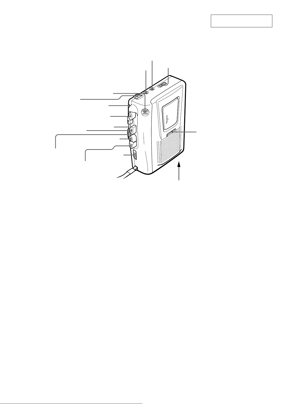
• Location of Controls
VOL
Built-in mic
BATT
z REC
SECTION 2
GENERAL
EAR
MIC
VOR
This section is extracted from
instruction manual.
B PLAY
SPEED CONTROL
M FF/CUE
x STOP
m REW/
REVIEW
PAUSE
.
REC TIME
DC IN 3 V
– 3 –
Page 4
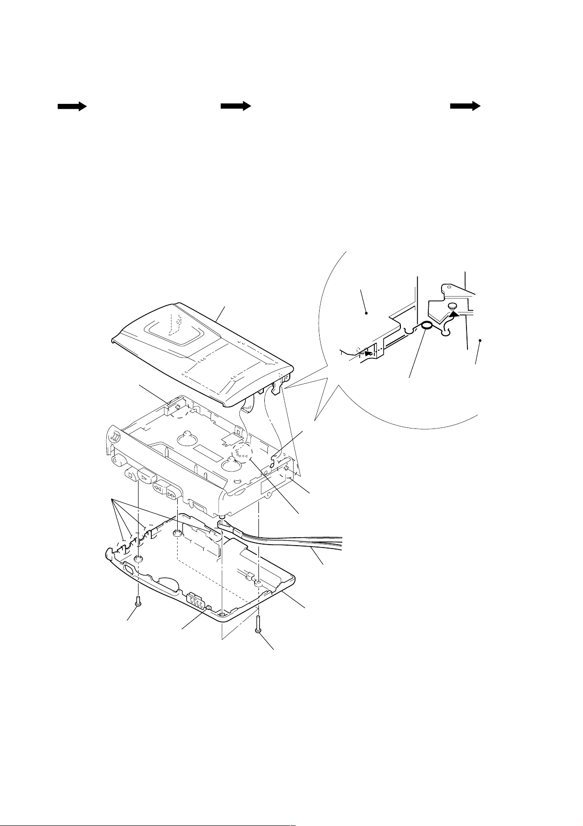
• This set can be disassembled in the order shown below.
T
G
SECTION 3
DISASSEMBLY
SET
Note: Follow the disassembly procedure in the numerical order given.
CABINET (REAR), CASSETTE LID
CABINET (REAR), CASSETTE LID
9 cassette lid
7 boss
MAIN BOARD, MECHANISM DECK (MT-20DV-118)
INSTALLATION CASSETTE SPRIN
cabinet front
cassette spring
BEL
cassette lid
3 four claws
2 screw
(IB lock)
7 boss
6 Remove the six solders.
5 hand strap
4 cabinet (rear)
3 claw
1 three screws
(B1.7 × 9)
– 4 –
Page 5
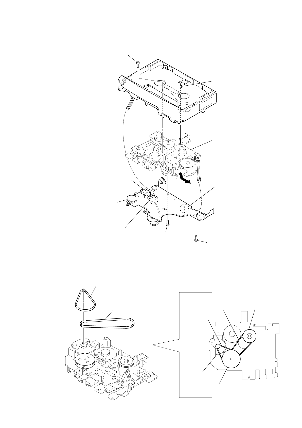
MAIN BOARD, MECHANISM DECK (MT-20DV-118)
5 three screws
(IB lock)
1 Remove the two solders
electret condenser microphone
(MIC101).
6 claw
7 mechanism deck
(MT-20DV-118)
1 Remove the two solders
motor (M901).
BELT
4 MAIN board
1 Remove the two solders
magnetic head (HRP901).
1 belt (capstan)
2 belt (FR)
3 screw
(M1.4)
2 screw
(1.7)
capstan belt
FR belt
pulley (FR) assy
– 5 –
motor DC
flywheel assy
Page 6

INSTALLATION MAIN BOARD
On installation MAIN board, adjust to the S101 and
the S102.
screw
(1.7)
S102
(POWER)
screw
(M1.4)
MAIN board
S101 (REC/PB)
lever (REC)
– 6 –
Page 7

SECTION 4
MECHANICAL ADJUSTMENTS
1. Clean the following parts with a denatured-alcohol-moistened
swab:
record/playback head pinch roller
erase head rubber belt
capstan idlers
2. Demagnetize the record/playback head with a head demagnetizer. (Do not bring the head demagnetizer close to the erase
head.)
3. Do not use a magnetized screwdriver for the adjustments.
4. After the adjustments, apply suitable locking compound to the
parts adjusted.
5. The adjustments should be performed with the rated power
supply voltage (2.5 V) unless otherwise noted.
Torque Measurement
Mode Torque Meter Meter Reading
FWD
CQ-102C
FWD
Back Tension
FF
REW (more than 0.69 oz•inch)
CQ-201B (more than 50 g•cm)
2.16 - 4.7 mN•m
(22 - 48 g•cm)
(0.31 - 0.67 oz•inch)
0.05 - 0.29 mN•m
(0.5 - 3 g•cm)
(0.007 - 0.04 oz•inch)
4.90 mN•m
T ape Tension Measurement
Mode Torque Meter Meter Reading
FWD CQ-403C (more than 50 g)
4.90 mN•m
(more than 1.76 oz)
– 7 –
Page 8

SECTION 5
r
j
)
ELECTRICAL ADJUSTMENTS
Setting:
• Supplied voltage: 2.5 V
• Switch and control position
[VOL ] control (RV101) : mechanical center
w
[PAUSE ] switch (S105) : OFF
.
[SPEED CONTROL](RV602): center click
[VOR] switch (S104) : OFF
Test T ape
Ty pe Signal Used for
P-4-A063 6.3 kHz, –10 dB Head Azimuth Adjustment
WS-48A 3 kHz, 0 dB Tape Speed Adjustment
0 dB=0.775 V
Record/Playback Head Azimuth Adjustment
Mode: playback
test tape
P-4-A063
(6.3 kHz, –10 dB)
set
EAR
Procedure:
1. Turn the adjustment scre w to obtain the maximum reading on
level meter.
Note: Several peaks may appear, but take the maximum.
2. After the adjustment, lock the adjustment screw with suitable
locking compound.
level mete
10 kΩ
+
–
ack (J102
Tape Speed Adjustment
Mode: playback
test tape
WS-48A
(3 kHz, 0 dB)
10 kΩ
set
EAR jack (J102)
frequency
counter
+
–
Procedure:
– Normal Speed –
1. Set [REC TIME] switch (S601) to NORMAL (4.8 cm/s) position, and playback the tape (WS-48A) .
2. Adjust RV601 so that frequency counter r eading becomes 3,040
Hz.
Specification values: 3,030 to 3,050 Hz
– Double Speed –
3. Set [REC TIME] switch (S601) to DOUBLE (2.4 cm/s) position.
4. Playback the tape from the beginning for two minutes, then
adjust R V603 so that frequency counter reading becomes 1,540
Hz.
Specification values: 1,535 to 1,545 Hz
Confirm that deflection of the frequency counter reading between
the beginning and the end of tape is within 1% (NORMAL: approx.
30.4 Hz, DOUBLE: approx. 15.4 Hz) .
Adjustment Location:
adjustment screw
Press the N
button.
Adjustment Location:
– MAIN BOARD (Conductor Side) –
J102 J101
RV601
Tape Speed Adjustment
(Normal Speed)
RV603
Tape Speed Adjustment
(Double Speed)
– 8 –
Page 9

6-1. BLOCK DIAGRAM
TCM-20DV/21DV/22DV/23DV
SECTION 6
DIAGRAMS
J101
MIC
(PLUG IN POWER)
HRP901
(REC/PB)
HE901
(ERASE)
MIC101
MIC
S101
(REC/PB)
PB
REC
S101 (1/6)
CONTROL
S101 (4/6)
VREF
Q101
AGC
28
29
5
4
MIC IN
EQ IN
ALC
CONT
REC OUT
MIC AMP, REC/PB EQ AMP
IC101 (1/3)
MIC
AMP
EQ
AMP
ALC
REC
AMP
POWER ON
B+
PRE
OUT
PRE
REC IN
• SIGNAL PATH
: PLAY
: RECORD
VREF
OFF
+
Q111
VOR ON
SWITCH
S101 (2/6)
(REC/PB)
PB
REC
REC B+
REC B+
Q105
VOR OFF
SWITCH
POWER AMP, VOR CONTROL,REGULATOR
POW IN
11
VOR
DELAY
7
R/P
SW
23
REC/PB
VOX
IC101 (2/3)
POWER
AMP
POW OUT 1
POW OUT 2
PAUSE
LED
DRIVE
PAUSE
12
14
24
22
D101
BATT
Q112
SWITCHING
POWER ON B+
Q104
PB EQ
SWITCH
2
NF
NF
1
Q103
REC EQ
SWITCH
3
+
REC B+
REC B+
RV101
VOL
BUFFER
S104
VOR
HL
REC B+
Q102
S101 (3/6)
PB B+
(REC/PB)
PB
REC
PAUSE .
S105
OFF
ON
Q106
REC/PB
MONITOR LEVEL
SWITCHING
PB B+
SP901
(SPEAKER)
J102
EAR
S101 (6/6)
(REC/PB)
05
PB
REC
POWER ON B+
RV602
SPEED CONTROL
S601-2
REC TIME
DOUBLE NORMAL
RV601
TAPE SPEED
(NORMAL SPEED)
THP602
RV601
M901
(CAPSTAN/REEL)
THP601
S601-1
REC TIME
DOUBLE NORMAL
RV603
TAPE SPEED
(DOUBLE SPEED)
M
CAPSTAN/REEL MOTOR DRIVE
VS
18
GVN VREF
19
GVN CONT
20
GVN OUT
16
IC101 (3/3)
MOTOR
DRIVER
VCC B+
PB B+
REC B+
VREF
S101 (5/6)
(REC/PB)
PB
REC
REFERENCE VOLTAGE
MUTE SWITCH
Q107, 108
MUTE
VCC
21
POWER ON B+
15
MUTE
MIC
VCC
REGULATOR
26
RIPPLE
REFERENCE
VREF
27
VOLTAGE
GENERATOR
FILTER
MUTE
SWITCH
Q109, 110
BATTERY B+
S102
(POWER)
REC B+
PB B+
DRY BATTERY
SIZE “AA”
(IEC DESIGNATION R6)
2PCS. 3V
CN101
DC IN 3V
+
–
– 9 – – 10 –
Page 10

TCM-20DV/21DV/22DV/23DV
6-2. PRINTED WIRING BOARDS
1
A
MAIN BOARD
B
C
D
Q112
E
S105
PAUSE
OFF
ON
F
2 3 4 5 6 7 8 9 10 11 12 13 14 15
(PLUG IN POWER)
C101
C146
–6
–5
–4
C112
+
C128
J101
MIC
BLK
C147
R103 R102 R105
C107
R112
R113
30
R122
16
R111
RED
C141
C106
C142
C132
R104
MIC101
MIC
C148
RV601
S102
(POWER)
R101
+
C104
C102
+
C105
Q101
E
D101
BATT
RV101
VOL
–2
–1
C136
R129
C149
Q102
C2
E2
R132
R131
R130
R134
R133
E1
B1
B2
C1
R106
B
C
C103
R601
R603
J102
EAR
C145
C124
+
C123
+
+
C122
(CONDUCTOR SIDE)
C134
Q104
C140
BCE
+
Q106
R119
E
C
B
Q103
R142
R137
C114
C111
BCE
C116
C110
C144
R118
C143
S101
(REC/PB)
REC PB
–3
–2
–1
12
R110
C108
+
R109
R114
C117
C121
C109
C118
R108
1
15
C127
+
IC101
C119
(COMPONENT SIDE)
S104
VOR
OFF L H
R201
R125
+
C133
R115
C137
R127
R126
BCE
R144
R604
Q108
BCE
Q107
BCE
R136
C138
R141
BCE
Q110
Q109
BCE
R123
C113
R116
R117
C130
Q111
BCE
R135
HRP901
(REC/PB HEAD)
HE901
(ERASE HEAD)
MAIN BOARD
1
2
C120
RV602
SPEED
CONTROL
R143
R138
R139
BCE
Q105
G
H
DRY BATTERY
SIZE “AA”
(IEC DESIGNATION R06)
2PCS. 3V
SP901
(SPEAKER)
+
C129
BRN
BRN
BRN
BRN
BLK
BLK
RV603
R606
R607
R610
THP601
R609
R602
THP602
C139
• Semiconductor Location
Ref. No. LocationRef. No. Location
D101 A-13
Q105 G-6
Q106 F-9
I
IC101 E-11
Q101 D-13
Q102 D-14
Q103 D-10
Q104 D-10
J
Note on Printed Wiring Boards:
• X : parts extracted from the component side.
Q107 F-3
Q108 E-3
Q109 E-3
Q110 F-3
Q111 C-7
Q112 E-2
• Y : parts extracted from the conductor side.
z
•
: Through hole.
• b : Pattern from the side which enables seeing.
(The other layers' patterns are not indicated.)
Caution:
Pattern face side: Parts on the pattern face side seen from
K
(Conductor Side) the pattern face are indicated.
Parts face side: Parts on the parts face side seen from
(Component Side) the parts face are indicated.
05
1-676-966-
11
(11)
– 11 –
M901
(CAPSTAN/REEL)
MM
BLK
RED
C125
C126
1-676-966-
SW BOARD
+
CN101
DC IN 3V
+–
11
(11)
BLK
BLK
BRN
BRN
S601
REC TIME
DOUBLE NORMAL
–1
–2
1-676-967-
11
– 12 –
Page 11

6-3. SCHEMATIC DIAGRAM • See page 15 for IC Block Diagram.
TCM-20DV/21DV/22DV/23DV
Note on Schematic Diagram:
• All capacitors are in µF unless otherwise noted. pF: µµF
50 WV or less are not indicated except for electrolytics
and tantalums.
• All resistors are in Ω and 1/
specified.
• C : panel designation.
• U : B+ Line.
• H : adjustment for repair.
• Total current is measured with no cassette installed.
• Power voltage is dc 3 V and fed with regulated dc power
supply from external power voltage jack.
4
W or less unless otherwise
– 13 – – 14 –
• Voltages are dc with respect to ground under no-signal
conditions.
no mark : PLAY
< > : RECORD
• Voltages are taken with a V OM (Input impedance 10 MΩ).
Voltage variations may be noted due to normal production tolerances.
• Signal path.
E : PLAY
a : RECORD
Page 12

SECTION 7
EXPLODED VIEWS
• IC Block Diagram
IC101 LA4168ML-TE-L
PRE GND
EQ IN
MIC IN
30
2.2k
+
–
EQ
300k
1
PRE NF
2
PRE OUT
+
–
MIC
3
REC IN
30k
+
4
Vref OUT
2k
–
20k
REC
REC OUT
MIC VCC
5
ALC CONT
R, F OUT
2526272829
ALC
6
VOX CONT
LED DRIVER/P SW
VOX
SPEED
VOX
7
VOX DELAY
PAUSE
MIC
VCC
+
–
Vref
8
GNV SPEED UP
PAUSE
222324
9
AUT STOP CONT
P/R MUTE
21
10
AUT STOP IN
GVN CONT
20
11
PWR IN
GVN Vref
1
12
PWR OUT1
1819
R/P
R, F
POWER
13
Vs
PWR GND
GVN GND
17
2
14
PWR OUT2
GVN
GVN OUT
16
15
Vcc
NOTE:
• -XX and -X mean standardized parts, so they
may have some difference from the original
one.
• Color Indication of Appearance Parts
Example:
KNOB, BALANCE (WHITE) . . . (RED)
↑↑
Parts Color Cabinet's Color
• Abbreviation
1E: No indication of country of origin
(1) CABINET SECTION
13
12
not
supplied
MIC101
11
28
10
7
9
8
MT-20DV-118
• Items marked “*” are not stocked since they
are seldom required for routine service. Some
delay should be anticipated when ordering
these items.
• The mechanical parts with no reference number in the exploded views are not supplied.
• Accessories and packing materials are given
in the last of the electrical parts list.
14
15
16
29
6
22
17
1
26
SP901
26
19
18
1
not
supplied
21
20
5
4
3
1
26
26
Ref. No. Part No. Description Remark
1 3-318-382-31 SCREW (1.7), TAPPING
2 3-345-648-01 SCREW (M1.4), TOOTHED LOCK
* 3 A-3021-314-A MAIN BOARD, COMPLETE
4 3-924-741-01 TERMINAL, PLUS
5 3-936-973-01 TERMINAL, MINUS
6 3-924-744-01 SPRING (CLAW DETECTION), TENSION
7 3-924-743-01 CLAW, ERASING PROTECTION
8 3-334-565-41 SCREW (B1.7), TAPPING
9 3-924-745-01 BAR, GROUND
10 3-924-740-01 HOLDER, MICROPHONE
11 3-924-763-01 CUSHION (MICROPHONE)
12 3-924-742-21 KNOB (VOR)
13 3-939-590-26 SCREW (IB LOCK)
14 3-578-101-31 PLATE, ORNAMENTAL
15 3-019-364-33 CABINET (FRONT) (20DV: 1E/23DV: 1E)
26
2
26
23
25
24
Ref. No. Part No. Description Remark
16 3-924-739-01 SPRING, CASSETTE
17 X-4952-666-1 LID ASSY, CASSETTE
18 4-017-441-01 CUSHION (B)
* 19 3-924-757-01 BRACKET (SPEAKER)
20 3-328-319-01 STRAP, HAND
21 3-924-749-21 LID, BATTERY CASE
22 3-924-747-21 KNOB (PAUSE)
23 3-019-597-11 CABINET (REAR)
24 3-318-203-92 SCREW (B1.7X9), TAPPING
25 3-366-890-51 SCREW (IB LOCK)
26 3-831-441-99 CUSHION
28 3-831-441-11 CUSHION, CABINET UPPER 10X7X0.5
* 29 1-676-967-11 SW BOARD
SP901 1-505-838-11 SPEAKER (3.6cm)
MIC101 1-542-136-11 MICROPHONE, ELECTRET CONDENSER
– 15 –
15 3-019-364-43 CABINET (FRONT) (20DV: 1E/23DV: 1E)
– 16 –
Page 13

(2) MECHANISM DECK SECTION-1
(MT-20DV-118)
61
60
56
58
62
63
HRP901
59
57
HE901
74
64
66
67
69
65
68
76
77
55
not
supplied
54
53
51
Ref. No. Part No. Description Remark
51 X-3377-250-1 LEVER, (2) ASSY, PINCH
52 3-925-146-01 BUTTON (FF) (M)
53 3-925-147-01 BUTTON (REW) (m)
54 3-925-148-01 BUTTON (PLAY) (N)
55 3-925-145-01 BUTTON (REC) (z)
56 3-924-738-01 BUTTON (STOP) (x)
57 3-703-925-21 SCREW (M1.4)
58 3-924-625-01 LEVER (HEAD)
59 3-924-645-01 BRACKET (HEAD)
60 3-924-685-01 SPRING (AZIMUTH), COMPRESSION
61 3-704-197-91 SCREW (M1.4X1.8), LOCKING
62 3-375-135-01 SCREW (1.4), SPECIAL
63 3-376-177-01 SCREW (M1.4X3.8)
64 3-925-107-01 SPRING (IDLER), COMPRESSION
65 3-924-637-01 GEAR (FF)
52
70
M901
75
71
78
73
72
Ref. No. Part No. Description Remark
67 3-924-674-01 SPRING (B. T), COMPRESSION
68 3-924-641-01 GEAR (T REEL)
69 3-924-726-01 SPRING (M GROUND), TORSION
70 3-907-943-01 BELT (CAPSTAN)
71 3-925-109-01 CUSHION (MOTOR)
72 3-925-108-01 SCREW (MOTOR)
73 3-924-644-01 SPRING (POWER TENSION), TENSION
74 3-348-160-11 SCREW (M1.4X1.6), PRECISION PAN
75 3-927-754-11 CUSHION (M)
76 3-831-441-99 CUSHION
77 3-030-766-12 SHEET (MOTOR)
78 3-561-685-01 SHEET (C), INSULATING
HE901 1-500-515-11 HEAD, MAGNETIC (ERASE)
HRP901 1-500-073-51 HEAD, MAGNETIC (RECORD/PLAYBACK)
M901 1-763-453-21 MOTOR, DC (CAPSTAN/REEL) (WITH PULLEY)
66 3-924-673-01 GEAR (S REEL)
– 17 –
Page 14

(3) MECHANISM DECK SECTION-2
(MT-20DV-118)
109
113
111110
112
116
114
103
107
106
102
105
108
104
101
not
supplied
118
124
120
121
127
117
101
119
115
123
122
128
129
125
102
101
Ref. No. Part No. Description Remark
101 3-321-483-11 RING, RETAINING (0.25)
102 3-315-495-31 WASHER
103 X-3370-384-1 FLYWHEEL ASSY
104 3-924-623-01 LEVER (PLAY)
105 3-924-621-01 LEVER (REW)
106 3-924-620-01 LEVER (FF)
107 X-3370-388-1 TABLE ASSY, FELT
108 3-924-642-01 SPRING (FR), TORSION
109 3-924-629-01 LEVER (DETECTION)
110 3-925-207-01 SPRING (S. OFF), TENSION
111 3-924-630-01 LEVER (S.OFF)
112 X-3370-387-1 LEVER ASSY, IDLER
113 3-924-682-01 BELT (FR)
114 X-3370-385-1 PULLEY (FR) ASSY
115 3-924-628-01 LEVER (FR)
126
Ref. No. Part No. Description Remark
116 3-924-633-01 SPRING (STOP), TENSION
117 3-924-622-01 LEVER (STOP)
118 3-924-643-01 SPRING (PR), TORSION
119 3-924-684-01 SPRING (LOCK PLATE), TENSION
120 3-924-619-01 LEVER (SW)
121 3-924-639-01 LEVER (CR)
122 3-924-618-01 LEVER (LOCK)
123 3-925-208-01 SPRING (REC), TENSION
124 3-924-624-01 LEVER (REC)
125 X-3372-155-1 CHASSIS ASSY
126 3-924-613-01 GEAR (FR)
127 3-024-378-01 SPRING (FR LEVER), TORSION
128 3-939-590-26 SCREW (IB LOCK)
129 3-029-566-12 STOPPER (FF)
– 18 –
Page 15

SECTION 8
ELECTRICAL PARTS LIST
MAIN
NOTE:
• Due to standardization, replacements in the
parts list may be different from the parts specified in the diagrams or the components used
on the set.
• -XX and -X mean standardized parts, so they
may have some difference from the original
one.
• RESISTORS
All resistors are in ohms.
METAL: Metal-film resistor.
METAL OXIDE: Metal oxide-film resistor.
F: nonflammable
• Abbreviation
1E: No indication of country of origin
Ref. No. Part No. Description Remark Ref. No. Part No. Description Remark
* A-3021-314-A MAIN BOARD, COMPLETE
*********************
3-924-741-01 TERMINAL, PLUS
< CAPACITOR >
C101 1-163-809-11 CERAMIC CHIP 0.047uF 10% 25V
C102 1-164-161-11 CERAMIC CHIP 0.0022uF 10% 100V
C103 1-109-982-11 CERAMIC CHIP 1uF 10% 10V
C104 1-135-201-11 TANTALUM CHIP 10uF 20% 4V
C105 1-135-201-11 TANTALUM CHIP 10uF 20% 4V
• Items marked “*” are not stocked since they
are seldom required for routine service.
Some delay should be anticipated when ordering these items.
• SEMICONDUCTORS
In each case, u: µ, for example:
uA. . : µA. . uPA. . : µPA. .
uPB. . : µPB. . uPC. . : µPC. .
uPD. . : µPD. .
• CAPACITORS
uF: µF
• COILS
uH: µH
C142 1-163-009-11 CERAMIC CHIP 0.001uF 10% 50V
C143 1-163-009-11 CERAMIC CHIP 0.001uF 10% 50V
C144 1-163-009-11 CERAMIC CHIP 0.001uF 10% 50V
C145 1-163-009-11 CERAMIC CHIP 0.001uF 10% 50V
C146 1-163-251-11 CERAMIC CHIP 100PF 5% 50V
C147 1-163-009-11 CERAMIC CHIP 0.001uF 10% 50V
C148 1-164-492-11 CERAMIC CHIP 0.15uF 10% 16V
C149 1-163-009-11 CERAMIC CHIP 0.001uF 10% 50V
The components identified by
mark 0 or dotted line with mark
0 are critical for safety.
Replace only with part number
specified.
Les composants identifiés par une
marque 0 sont critiquens pour la
sécurité.
Ne les remplacer que par une pièce
portant le numéro spécifié.
When indicating parts by reference
number, please include the board.
< CONNECTOR >
C106 1-163-009-11 CERAMIC CHIP 0.001uF 10% 50V
C107 1-107-725-11 CERAMIC CHIP 0.1uF 10% 16V
C108 1-163-017-00 CERAMIC CHIP 0.0047uF 5% 50V
C109 1-163-001-11 CERAMIC CHIP 220PF 10% 50V
C110 1-109-982-11 CERAMIC CHIP 1uF 10% 10V
C111 1-135-151-21 TANTALUM CHIP 4.7uF 20% 4V
C112 1-163-017-00 CERAMIC CHIP 0.0047uF 5% 50V
C113 1-164-005-11 CERAMIC CHIP 0.47uF 25V
C114 1-164-346-11 CERAMIC CHIP 1uF 16V
C116 1-164-346-11 CERAMIC CHIP 1uF 16V
C117 1-163-009-11 CERAMIC CHIP 0.001uF 10% 50V
C118 1-164-489-11 CERAMIC CHIP 0.22uF 10% 16V
C119 1-164-489-11 CERAMIC CHIP 0.22uF 10% 16V
C120 1-126-153-11 ELECT 22uF 20% 6.3V
C121 1-163-009-11 CERAMIC CHIP 0.001uF 10% 50V
C122 1-126-153-11 ELECT 22uF 20% 6.3V
C123 1-124-257-00 ELECT 2.2uF 20% 50V
C124 1-124-259-11 ELECT 4.7uF 20% 16V
C125 1-124-434-00 ELECT 220uF 20% 4V
C126 1-164-346-11 CERAMIC CHIP 1uF 16V
C127 1-124-434-00 ELECT 220uF 20% 4V
C128 1-124-433-00 ELECT 100uF 20% 4V
C129 1-126-153-11 ELECT 22uF 20% 6.3V
C130 1-163-038-00 CERAMIC CHIP 0.1uF 25V
C132 1-164-346-11 CERAMIC CHIP 1uF 16V
CN101 1-580-919-11 JACK, DC (POLARITY UNIFIED TYPE)
(DC IN 3V)
< DIODE >
D101 8-719-057-27 LED L-132XHD (BATT)
< IC >
IC101 8-759-492-49 IC LA4168ML-TE-L
< JACK >
J101 1-766-847-12 JACK (MIC PLUG IN POWER)
J102 1-766-847-12 JACK (EAR)
< TRANSISTOR >
Q101 8-729-800-37 TRANSISTOR 2SD1048-X7
Q102 8-729-402-84 TRANSISTOR XN4601
Q103 8-729-420-50 TRANSISTOR UN5215
Q104 8-729-230-72 TRANSISTOR 2SA1362YG
Q105 8-729-230-63 TRANSISTOR 2SC4116-YG
Q106 8-729-800-37 TRANSISTOR 2SD1048-X7
Q107 8-729-420-53 TRANSISTOR UN5115
Q108 8-729-402-93 TRANSISTOR UN5214-TX
Q109 8-729-420-53 TRANSISTOR UN5115
Q110 8-729-420-50 TRANSISTOR UN5215
C133 1-135-151-21 TANTALUM CHIP 4.7uF 20% 4V
C134 1-164-182-11 CERAMIC CHIP 0.0033uF 10% 50V
C136 1-164-346-11 CERAMIC CHIP 1uF 16V
C137 1-164-346-11 CERAMIC CHIP 1uF 16V
C138 1-164-346-11 CERAMIC CHIP 1uF 16V
C139 1-164-505-11 CERAMIC CHIP 2.2uF 16V
C140 1-163-009-11 CERAMIC CHIP 0.001uF 10% 50V
C141 1-163-009-11 CERAMIC CHIP 0.001uF 10% 50V
Q111 8-729-402-93 TRANSISTOR UN5214-TX
Q112 8-729-420-50 TRANSISTOR UN5215
< RESISTOR >
R101 1-216-065-00 RES-CHIP 4.7K 5% 1/10W
R102 1-216-053-00 METAL CHIP 1.5K 5% 1/10W
R103 1-216-069-00 METAL CHIP 6.8K 5% 1/10W
R104 1-216-073-00 METAL CHIP 10K 5% 1/10W
– 19 –
Page 16

TCM-20DV/21DV/22DV/23DV
MAIN SW
Ref. No. Part No. Description Remark
R105 1-216-049-11 RES-CHIP 1K 5% 1/10W
R106 1-216-049-11 RES-CHIP 1K 5% 1/10W
R108 1-216-085-00 METAL CHIP 33K 5% 1/10W
R109 1-216-037-00 METAL CHIP 330 5% 1/10W
R110 1-216-037-00 METAL CHIP 330 5% 1/10W
R111 1-216-069-00 METAL CHIP 6.8K 5% 1/10W
R112 1-216-073-00 METAL CHIP 10K 5% 1/10W
R113 1-216-089-00 RES-CHIP 47K 5% 1/10W
R114 1-216-081-00 METAL CHIP 22K 5% 1/10W
R115 1-216-065-00 RES-CHIP 4.7K 5% 1/10W
R116 1-216-089-00 RES-CHIP 47K 5% 1/10W
R117 1-216-065-00 RES-CHIP 4.7K 5% 1/10W
R118 1-216-009-00 RES-CHIP 22 5% 1/10W
R119 1-216-121-00 RES-CHIP 1M 5% 1/10W
R122 1-216-081-00 METAL CHIP 22K 5% 1/10W
R123 1-216-057-00 METAL CHIP 2.2K 5% 1/10W
R125 1-216-065-00 RES-CHIP 4.7K 5% 1/10W
R126 1-216-033-00 METAL CHIP 220 5% 1/10W
R127 1-216-053-00 METAL CHIP 1.5K 5% 1/10W
R129 1-216-097-00 RES-CHIP 100K 5% 1/10W
R130 1-216-061-00 METAL CHIP 3.3K 5% 1/10W
R131 1-216-077-00 RES-CHIP 15K 5% 1/10W
R132 1-216-061-00 METAL CHIP 3.3K 5% 1/10W
R133 1-216-045-00 METAL CHIP 680 5% 1/10W
R134 1-216-061-00 METAL CHIP 3.3K 5% 1/10W
R135 1-216-105-00 RES-CHIP 220K 5% 1/10W
R136 1-216-097-00 RES-CHIP 100K 5% 1/10W
R137 1-216-073-00 METAL CHIP 10K 5% 1/10W
R138 1-216-097-00 RES-CHIP 100K 5% 1/10W
R139 1-216-105-00 RES-CHIP 220K 5% 1/10W
R141 1-216-073-00 METAL CHIP 10K 5% 1/10W
R142 1-216-025-00 RES-CHIP 100 5% 1/10W
R143 1-216-065-00 RES-CHIP 4.7K 5% 1/10W
R144 1-216-017-00 RES-CHIP 47 5% 1/10W
R201 1-216-009-00 RES-CHIP 22 5% 1/10W
R601 1-216-081-00 METAL CHIP 22K 5% 1/10W
R602 1-216-049-11 RES-CHIP 1K 5% 1/10W
R603 1-216-053-00 METAL CHIP 1.5K 5% 1/10W
R604 1-216-077-00 RES-CHIP 15K 5% 1/10W
R606 1-216-097-00 RES-CHIP 100K 5% 1/10W
R607 1-216-081-00 METAL CHIP 22K 5% 1/10W
R609 1-216-053-00 METAL CHIP 1.5K 5% 1/10W
R610 1-216-057-00 METAL CHIP 2.2K 5% 1/10W
< VARIABLE RESISTOR >
RV101 1-227-166-11 RES, VAR, CARBON (VOL w)
RV601 1-223-583-11 RES, ADJ, CARBON 1K
RV602 1-225-598-11 RES, VAR, CARBON 2K (SPEED CONTROL)
RV603 1-223-587-11 RES, ADJ, CARBON 22K
Ref. No. Part No. Description Remark
< THERMISTOR >
THP601 1-810-007-11 THERMISTOR, POSITIVE
THP602 1-809-350-21 THERMISTOR, NTC (2125)
**************************************************************
* 1-676-967-11 SW BOARD
*********
< SWITCH >
S601 1-571-277-51 SWITCH, SLIDE (REC TIME)
**************************************************************
MISCELLANEOUS
**************
HE901 1-500-515-11 HEAD, MAGNETIC (ERASE)
HRP901 1-500-073-51 HEAD, MAGNETIC (RECORD/PLAYBACK)
M901 1-763-453-21 MOTOR, DC (CAPSTAN/REEL) (WITH PULLEY)
MIC101 1-542-136-11 MICROPHONE, ELECTRET CONDENSER (MIC)
SP901 1-505-838-11 SPEAKER (3.6cm)
************************************************************
ACCESSORIES & PACKING MATERIALS
*********************************
0 1-528-405-31 ADAPTOR, BATTERY CHARGE
(BCA-35E) (22DV)
1-542-307-11 MICROPHONE (ECM-J2SL) (21DV)
0 1-693-073-21 ADAPTOR, AC (AC-E350) (22DV)
1-756-035-31 BATTERY PACK (NC-WMAA) (22DV)
3-044-622-01 POUCH, CARRYING (21DV)
3-868-083-11 MANUAL, INSTRUCTION
(ENGLISH, FRENCH, SPANISH) (US, Canadian)
3-868-083-21 MANUAL, INSTRUCTION
(ENGLISH, SPANISH, PORTUGUESE) (E)
3-868-083-31 MANUAL, INSTRUCTION
(GERMAN, ITALIAN, HUNGARIAN) (21DV: E)
3-868-083-41 MANUAL, INSTRUCTION
(FRENCH, GERMAN, ITALIAN) (20DV: E)
3-868-083-51 MANUAL, INSTRUCTION
(DUTCH, SWEDISH, FINNISH) (20DV: E)
3-868-083-61 MANUAL, INSTRUCTION (POLISH, CZECH,
SLOVAKIAN) (20DV: EE/21DV: E)
3-868-083-71 MANUAL, INSTRUCTION (ENGLISH, CHINESE)
(20DV: 1E/23DV: 1E)
3-868-083-81 MANUAL, INSTRUCTION (ENGLISH, CHINESE)
(20DV: CHINESE)
3-868-083-91 MANUAL, INSTRUCTION
(ENGLISH, RUSSIAN, HUNGARIAN) (20DV: EE)
8-814-296-90 MICROPHONE, CONDENSER ECM-TC60
(23DV)
< SWITCH >
S101 1-771-321-11 SWITCH, SLIDE (REC/PB)
S102 1-572-688-11 SWITCH, PUSH (1 KEY) (POWER)
S104 1-692-605-31 SWITCH, SLIDE (VOR)
S105 1-572-922-11 SWITCH, SLIDE (PAUSE .)
9-927-668-11
The components identified by
mark 0 or dotted line with
mark 0 are critical for safety .
Replace only with part number specified.
Sony Corporation
Personal Audio Division Company
– 20 –
Les composants identifiés par une
marque 0 sont critiques pour la
sécurité.
Ne les remplacer que par une pièce
portant le numéro spécifié.
Published by General Engineering Dept.
Printed in Japan C 2000. 2
2000B0579-1
 Loading...