Sony TAWR-4 Service manual
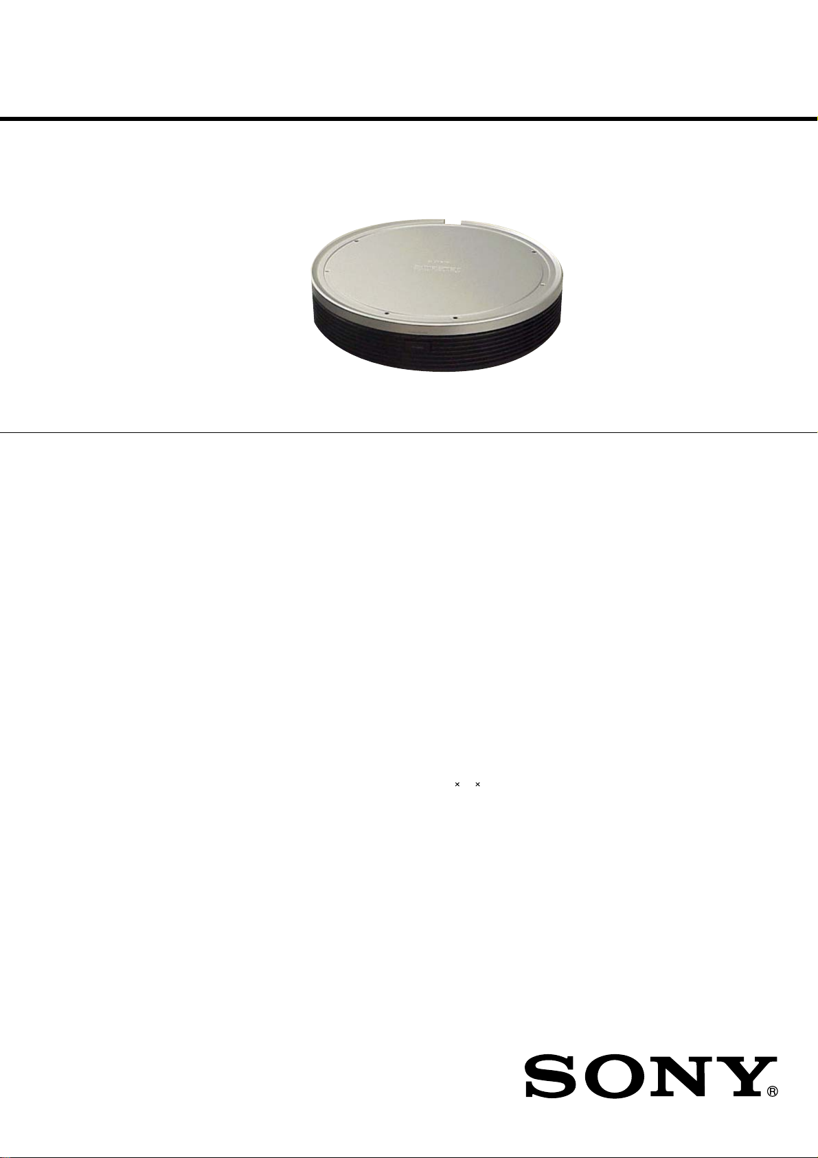
TA-WR4
SERVICE MANUAL
Ver. 1.2 2006.09
TA-WR4 is the surround amplifier section
in DAV-DZ810W/DZ820KW/FX900W/
FX900KW.
SPECIFICATIONS
POWER OUTPUT AND
TOTAL HARMONIC
D
ISTORTION
(FTC Output Power)
US and Canadian models
Surround mode (reference) RMS output power, 10 %
Latin American models: 130 W + 130 W
Argentine and other models:
Power requirements
Latin American models: 110 - 240 V AC, 50/60 Hz
US and Canadian models
Other models: 220 - 240 V AC, 50/60 Hz
Taiwan model :
Power consumption 50 W
Dimensions (approx.) 280 60 280 mm (w/h/d)
Mass (approx.) 1.6 kg
:
SL/SR: 84 W/ch 3 ohms at
160 - 20,000 Hz,
0.7 % THD
THD
(with SS-TS55,
SS-TS56W)
140 W + 140 W
(with SS-TS55,
SS-TS56W)
120 V AC, 60 Hz
:
120 V AC, 50/60 Hz
US Model
Canadian Model
AEP Model
UK Model
E Model
Australian Model
9-887-226-03
2006I16-1
© 2006.09
Design and specifications are subject to change
without notice.
SURROUND AMPLIFIER
Sony Corporation
Home Audio Division
Published by Sony Techno Create Corporation
TA-WR4
r
Notes on chip component replacement
• Never reuse a disconnected chip component.
• Notice that the minus side of a tantalum capacitor may be
damaged by heat.
Flexible Circuit Board Repairing
• Keep the temperature of the soldering iron around 270 °C
during repairing.
• Do not touch the soldering iron on the same conductor of the
circuit board (within 3 times).
• Be careful not to apply force on the conductor when soldering
or unsoldering.
UNLEADED SOLDER
Boards requiring use of unleaded solder are printed with the leadfree mark (LF) indicating the solder contains no lead.
(Caution: Some printed circuit boards may not come printed with
the lead free mark due to their particular size)
: LEAD FREE MARK
Unleaded solder has the following characteristics.
• Unleaded solder melts at a temperature about 40 °C higher
than ordinary solder.
Ordinary soldering irons can be used but the iron tip has to be
applied to the solder joint for a slightly longer time.
Soldering irons using a temperature regulator should be set to
about 350 °C.
Caution: The printed pattern (copper foil) may peel away if
the heated tip is applied for too long, so be careful!
• Strong viscosity
Unleaded solder is more viscou-s (sticky, less prone to flow)
than ordinary solder so use caution not to let solder bridges
occur such as on IC pins, etc.
• Usable with ordinary solder
It is best to use only unleaded solder but unleaded solder may
also be added to ordinary solder.
SAFETY-RELATED COMPONENT WARNING!!
COMPONENTS IDENTIFIED BY MARK 0 OR DOTTED LINE
WITH MARK 0 ON THE SCHEMATIC DIAGRAMS AND IN
THE PARTS LIST ARE CRITICAL TO SAFE OPERATION.
REPLACE THESE COMPONENTS WITH SONY PARTS WHOSE
PART NUMBERS APPEAR AS SHOWN IN THIS MANUAL OR
IN SUPPLEMENTS PUBLISHED BY SONY.
ATTENTION AU COMPOSANT AYANT RAPPORT
À LA SÉCURITÉ!
LES COMPOSANTS IDENTIFÉS P AR UNE MARQUE 0 SUR LES
DIAGRAMMES SCHÉMA TIQUES ET LA LISTE DES PIÈCES SONT
CRITIQUES POUR LA SÉCURITÉ DE FONCTIONNEMENT. NE
REMPLACER CES COMPOSANTS QUE PAR DES PIÈSES SONY
DONT LES NUMÉROS SONT DONNÉS DANS CE MANUEL OU
DANS LES SUPPÉMENTS PUBLIÉS PAR SONY.
TABLE OF CONTENTS
1. GENERAL ................................................................... 3
2. DIAGRAMS
2-1. Block Diagram ................................................................ 5
2-2. Printed Wiring Board — RX AMP Board —................. 6
2-3. Schematic Diagram — RX AMP Board (1/4) — ........... 7
2-4. Schematic Diagram — RX AMP Board (2/4) — ........... 8
2-5. Schematic Diagram — RX AMP Board (3/4) — ........... 9
2-6. Schematic Diagram — RX AMP Board (4/4) — ........... 10
2-7. Printed Wiring Boards — Power Section — .................. 11
2-8. Schematic Diagram — Power Section — ...................... 12
3. EXPLODED VIEWS
3-1. Overall Section ................................................................ 20
3-2. AMP Section ................................................................... 21
4. ELECTRICAL PARTS LIST .................................. 22
SAFETY CHECK-OUT
After correcting the original service problem, perform the following
safety check before releasing the set to the customer:
Check the antenna terminals, metal trim, “metallized” knobs, screws,
and all other exposed metal parts for AC leakage.
Check leakage as described below.
LEAKAGE TEST
The AC leakage from any exposed metal part to earth ground and
from all exposed metal parts to any exposed metal part having a
return to chassis, must not exceed 0.5 mA (500 microamperes.).
Leakage current can be measured by any one of three methods.
1. A commercial leakage tester, such as the Simpson 229 or RCA
WT -540A. Follow the manuf acturers’ instructions to use these
instruments.
2. A battery-operated A C milliammeter . The Data Precision 245
digital multimeter is suitable for this job.
3. Measuring the voltage drop across a resistor by means of a
VOM or battery-operated AC v oltmeter. The “limit” indication
is 0.75 V, so analog meters must hav e an accurate low-voltage
scale. The Simpson 250 and Sanwa SH-63Trd are examples
of a passive VOM that is suitable. Nearly all battery operated
digital multimeters that have a 2 V A C range are suitable. (See
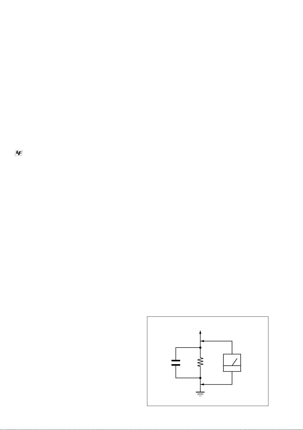
Fig. A)
To Exposed Metal
Parts on Set
AC
1.5 k
0.15 µF
Ω
Earth Ground
voltmete
(0.75 V)
Fig. A. Using an AC voltmeter to check AC leakage.
2
Surround amplifier
TA-WR4
SECTION 1
GENERAL
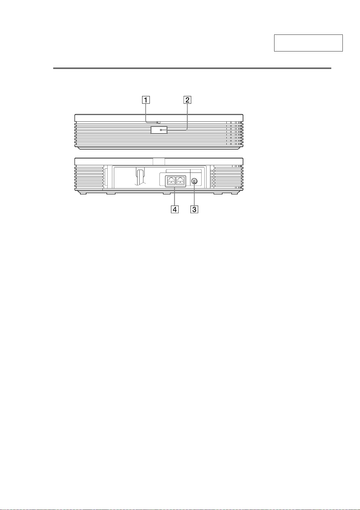
This section is extracted
from instruction manual.
POWER / ON LINE
A POWER/ON LINE indicator (23)
B POWER (23)
POWER
SPEAKER
SUR L SUR R
Front panel
SS-TS56W
Rear panel
C SS-TS56W jack (16)
D SPEAKER jacks (16)
3
TA-WR4
Ver. 1.2
SECTION 2
DIAGRAMS
• Note for Printed Wiring Boards and Schematic Diagrams
Note on Printed Wiring Boards:
• X : parts extracted from the component side.
• Y : parts extracted from the conductor side.
• f : internal component.
• : Pattern from the side which enables seeing.
(The other layers' patterns are not indicated.)
Caution:
Parts face side: Parts on the parts face side seen from
(SIDE A) the parts face are indicated.
Pattern face side: Parts on the pattern face side seen from
(SIDE B) the pattern face are indicated.
• Indication of transistor.
C
Q
B
E
B
These are omitted.
Q
CE
These are omitted.
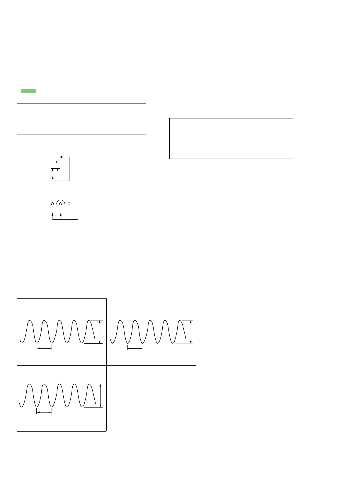
•Waveforms
– RX AMP Board –
Note on Schematic Diagrams:
• All capacitors are in µF unless otherwise noted. (p: pF)
50 WV or less are not indicated except f or electrolytics and
tantalums.
• All resistors are in Ω and 1/
specified.
• f : internal component.
• 2 : nonflammable resistor.
• C : panel designation.
Note:
The components identified by mark 0 or dotted line with mark 0 are
critical for safety.
Replace only with part
number specified.
• A : B+ Line.
•Voltages and waveforms are dc with respect to ground
under no-signal (detuned) conditions.
no mark: Power on
•Voltages are taken with a VOM (Input impedance 10 MΩ).
Voltage v ariations ma y be noted due to normal production
tolerances.
•Waveforms are taken with a oscilloscope.
Voltage v ariations ma y be noted due to normal production
tolerances.
• Circled numbers refer to waveforms.
• Signal path.
F : AUDIO
•Abbreviation
AR : Argentina model
AUS: Australian model
CND : Canadian model
E3 : 240V AC area in E model
E32 : 110-240V AC area in E model
KR : Korean model
RU : Russian model
SP : Singapore model
TW : T aiwan model
4
W or less unless otherwise
Note:
Les composants identifiés
par une marque 0 sont critiques pour la sécurité.
Ne les remplacer que par une
piéce portant le numéro
spécifié.
1
IC107 wd (X1)
125 ns
1 V/DIV, 100 ns/DIV
2
IC102 r; (OSCI)
81.3 ns
1 V/DIV, 40 ns/DIV
3.7 Vp-p
4.1 Vp-p
3
IC301 rk (XFSOIN)
20.3 ns
1 V/DIV, 10 ns/DIV
3.7 Vp-p
4
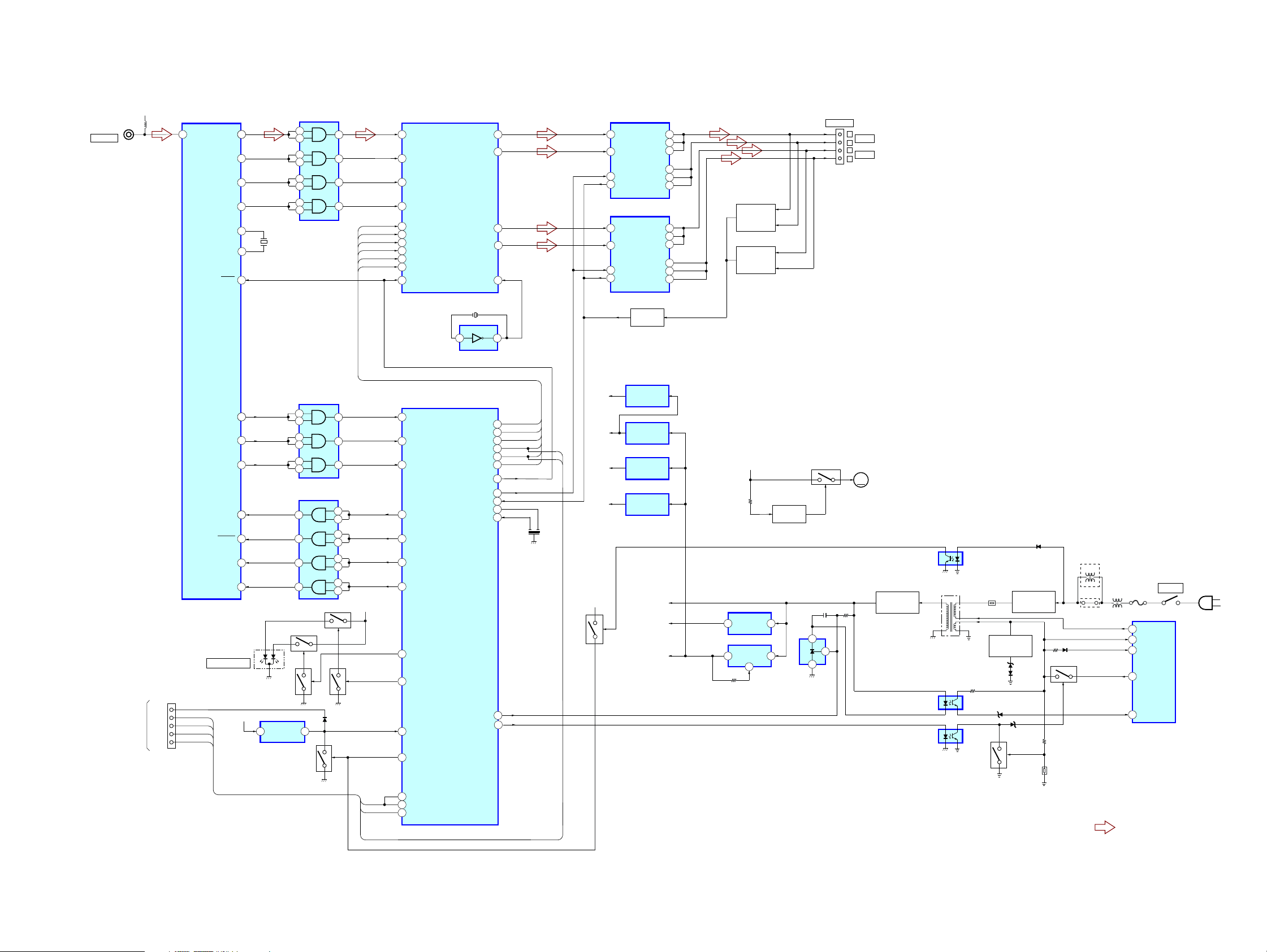
2-1. BLOCK DIAGRAM
TA-WR4
Ver. 1.2
J310
SS-TS56W
FOR FLASH
(
PROGRAMMING
5V
L304
CN303
RESET
SCK2
SO2
(
MOD
SI2
RF DEMODULATOR
A/D CONVERTER
10
ADVIN
(1)
(2)
(3)
(4)
IC102
DAOUT/
ROUT
BCK/
RCLK
APX
LRCK/
RCS
OSCI
OSCO
XRST
DTVALID
CSOD
SRDT
SCMODE
XSCEN
SCLK
SWDT
D100
POWER/ON LINE
31
60
54
31
59
40
43
13
31
61
33
34
31
38
36
37
35
3.3V
DATA
BCK
APX
LRCK
GREEN
X101
12.288MHz
RED
2 1
VDD
IC105
RESET
Q306
OUT
11
4
5
1
2
12
13
9
10
4
5
9
10
12
13
3
6
8
Q309
IC109
AND GATE
IC106
AND GATE
IC103
AND GATE
Q305
6
3
11
8
6
8
11
1
2
4
5
12
13
9
10
Q310 5V
Q307
SCLK
SWDT
31
30
36
29
18
19
20
21
22
23
27
14
15
53
48
50
51
52
42
41
19
17
DATA
BCK
XFSIIN
LRCK
NSPMUTE
SOFTMUTE
PGMUTE
SCDT
SCSHIFT
SCLATCH
INIT
DTVALID
CSOD
DIAT_SRDT
SCMODE
XSCEN
DIAT SCLK
DIAT SWDT
LED RED
LED GREEN
/RESET
AC CUT
IC301
STREAM PROCESSOR
49.152MH
2 4
IC107
SYSTEM CONTROLLER
DAMP_NSPMUTE
DAMP_SOFTMUTE
DAMP_PGMUTE
DAMP_SCDT
DAMP_SHIFT
DAMP_LATCH
XRST_INIT
DRIVE RST
DRIVE OCP
OUTL1
OUTL2
OUTR1
OUTR2
XFSOIN
X3051
IC3051
OSC
V CONT
MAIN OFF
IC100
POWER AMP
3.3V
1.8V
3.3V
2.5V
1.5V
6
PWM_A
14
PWM_B
5
/RESET
4
/SD
6
PWM_A
14
PWM_B
5
/RST
4
/SD
V CONT
MAIN OFF
IC200
POWER AMP
AC CUT
11
9
6
4
48
Z
35
34
33
61
60
59
26
37
38
22
XO
23
XI
58
57
X102
8MHZ
(1)
(2)
Q308
OUT A
OUT A
OUT A
OUT B
OUT B
OUT B
OUT A
OUT A
OUT A
OUT B
OUT B
OUT B
Q3551
PROTECT
IC113
1.8V REG
IC108
3.3V REG
IC104
2.5V REG
IC101
1.5V REG
30
29
28
27
26
25
Q110,111
OVER LOAD
2
DETECT
Q210,211
OVER LOAD
DETECT
12V
IC111
12V REG
IC110
5V REG
5
24
6
Q113
SWITCH
SHUNT REG
30
29
28
27
26
25
30V
12V
5V
IC905
T100
SPEAKER
-
SUR R
+
-
SUR L
+
Q117
3
2
1
M901
M
FAN
D921
RECT
PC902
T901
DC CONVERTER
PC901
PC903
TH901
LEVEL SHIFT
Q903
Q901
D911
D901
MAIN RECT
TH902
Q902
EXCEPT US, CND,
E32, TW
LF902
LF901
US, CND,
E32, TW
F901
SWITCHING
1
D
4
VCC
7
OCP/BD
5
SS/OLP
6
FB
IC901
S901
POWER
AC IN
TA-WR4
21
(3)
(4)
MOD1
20
MOD0
62
SI2
• Signal Path
: AUDIO
55
TA-WR4
Ver. 1.1
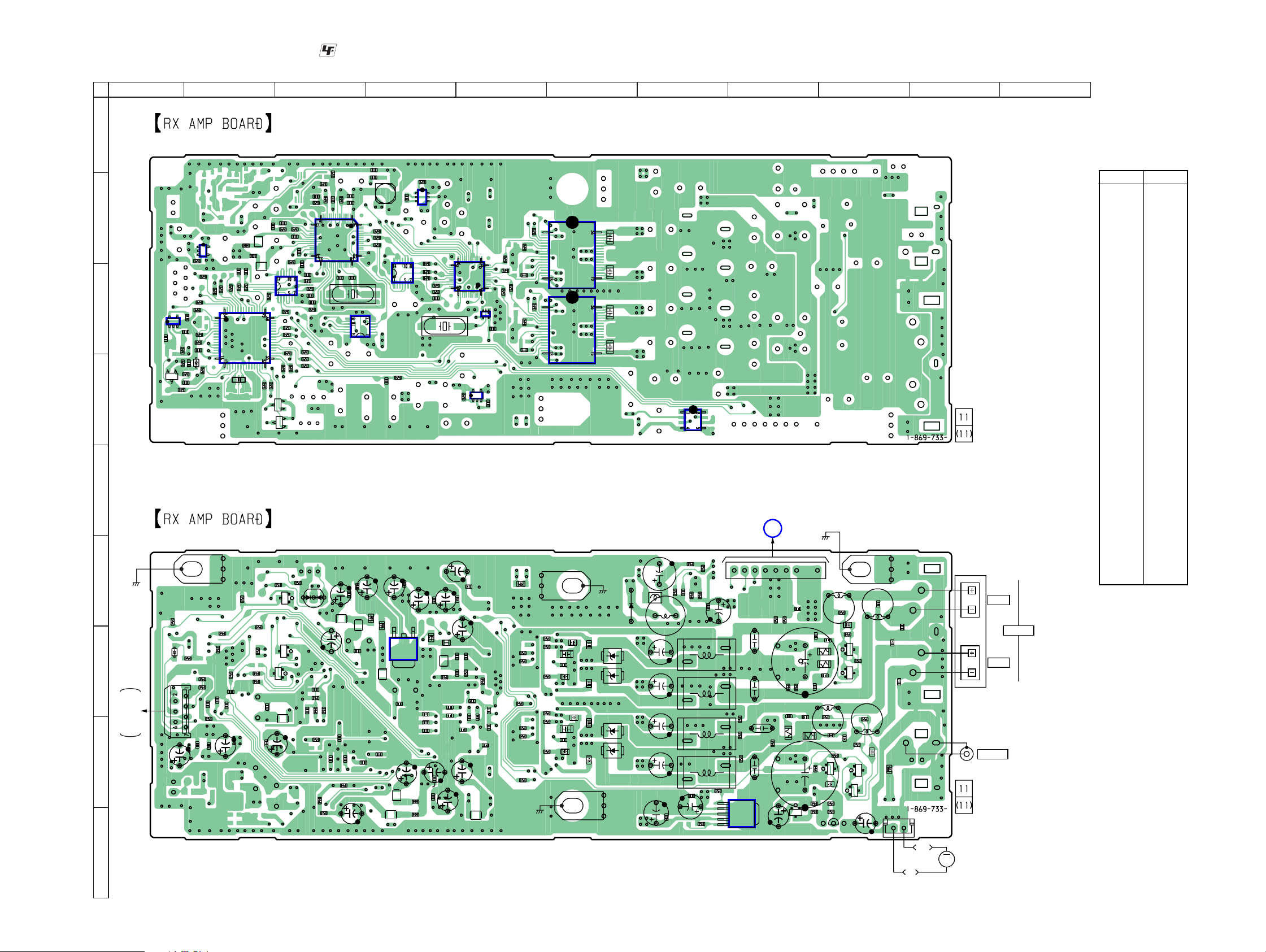
2-2. PRINTED WIRING BOARD — RX AMP BOARD —
:Uses unleaded solder.
A
B
C
D
E
F
G
H
1
(SIDE A)
IC105
514
3
C355
C357
R335
R336
E
R337
Q305
R344
IC101
R340
C354
C351
2 3 4 5 6 7 8 9 10 11
C336
C317
135
R317
R349
C366
C356
R345
R381
D303
R380
4
R367
R352
R355
FB101
FB102
C368
R359
R350
IC107
X102
C370
R360
R377
C321
L305
R356
C322
R318
C324
R326
L306
IC103
R366
R363
R361
R376
E
E
R364
R365
Q310
Q309
R319
C319
R362
R322
C333
C327
C330
R325
R383
R384
R385
R327
C334
C331
R328
R311
R324
C329
R323
IC102
C332
R329
C337
C340
C339
L304
R333
R331
R332
X101
IC106
C350
IC109
R382
C395
R330
135
IC104
R369
R370
4
R371
R3016
R368
C378
X3051
IC301
IC113
54
13
R374
R101
R102
13
IC3051
54
C415
C391
R202
R106
R110
R201
R206
R210
R104
R204
IC100
IC200
C106
C108C206
C208
IC110
• Semiconductor
Location
Ref. No.
D100 F-3
D101 H-6
D102 H-6
D201 G-6
D202 G-6
D303 D-2
D304 G-2
D306 F-6
IC100 B-6
IC101 B-2
IC102 B-3
IC103 C-3
IC104 B-4
IC105 C-1
IC106 C-4
IC107 C-2
IC108 G-4
IC109 B-4
IC110 D-7
IC111 H-8
IC113 D-5
IC200 C-6
IC301 C-5
IC3051 C-5
Location
Q110 H-9
Q111 H-9
Q113 I-8
Q117 I-8
Q210 G-9
Q211 G-9
DIAT POWER
BOARD
A
CN106
C211
C210
C110
C265
R221
C114
R119
CNP904
(Page 11)
R222
R220
E
Q113
C392
C220
R219
C115
R114
R115
C120
(CHASSIS)
18
C215
C214
R215
R214
C213
C212
R3554
R271
R267
L112
E
C421
C113
Q3551
R270
Q117
L212
R218
R269
R216
E
E
EB301
C218
L211
C216
Q211
R217
Q210
R116
C112
L111
R117R3555
Q111
E
E
Q110
C260
E
C118
C116
FB109
CN104
12
C217
C117
BLACK
RED
T100
SUR L
SPEAKER
SUR R
J310
SS-TS56W
M901
M
FAN
(SIDE B)
(CHASSIS)
FOR
FLASH
PROGRAMMING
C314
R346
D304
R348
CN303
R379
R347
EB102
C364
C313
R354
R353
C315
R399
C367
C365
C363
R357
C316
R373
R339
R372
R358
R338
R378
C341
C320
L309
Q308
E
E
Q306
E
R316
Q307
C318
D100
C325
R341
C361
R321
R314
C326
R320
R313
C328
C359
R342
R312
L311
C336
C335
C338
C358
C369
C360
C349
C371
L310
C353
L307
FB105
L312
C342
C373
FB106
31
IC108
C375
C377
C379
C376
L308
FB104
FB103
C372
C348
C380
FB3051
C343
C346
C387
R3053
C388
L3053
C407
C406
C344
C389
C345
L3054
C405
C383
C390
C418
C417
C413
C411
C416
R3052
L3055
C414
C404
C401
C412
R3054
C402
C403
R209
R207
FB107
R223
R109
R108
R123
(CHASSIS)
R213
R212
R203
R113
R112
R103
EB302
C202
C102
C219
C101
C201
C119
C203
C103
(CHASSIS)
D202
C205
C204
C105
C104
EB101
D201
D102
D101
D306
L313
C385
C209
C207
C109
C107
L314
C409
C382
R386
R388
C384
C386
C311
R390
L201
L202
L102
L101
R395
R389
C410
R387
R397
C381
IC111
1
5
R122
R121
R120
C111
I
Q305 D-1
Q306 G-3
Q307 G-3
Q308 F-3
Q309 D-3
Q310 D-3
Q3551 H-9
TA-WR4
66
TA-WR4
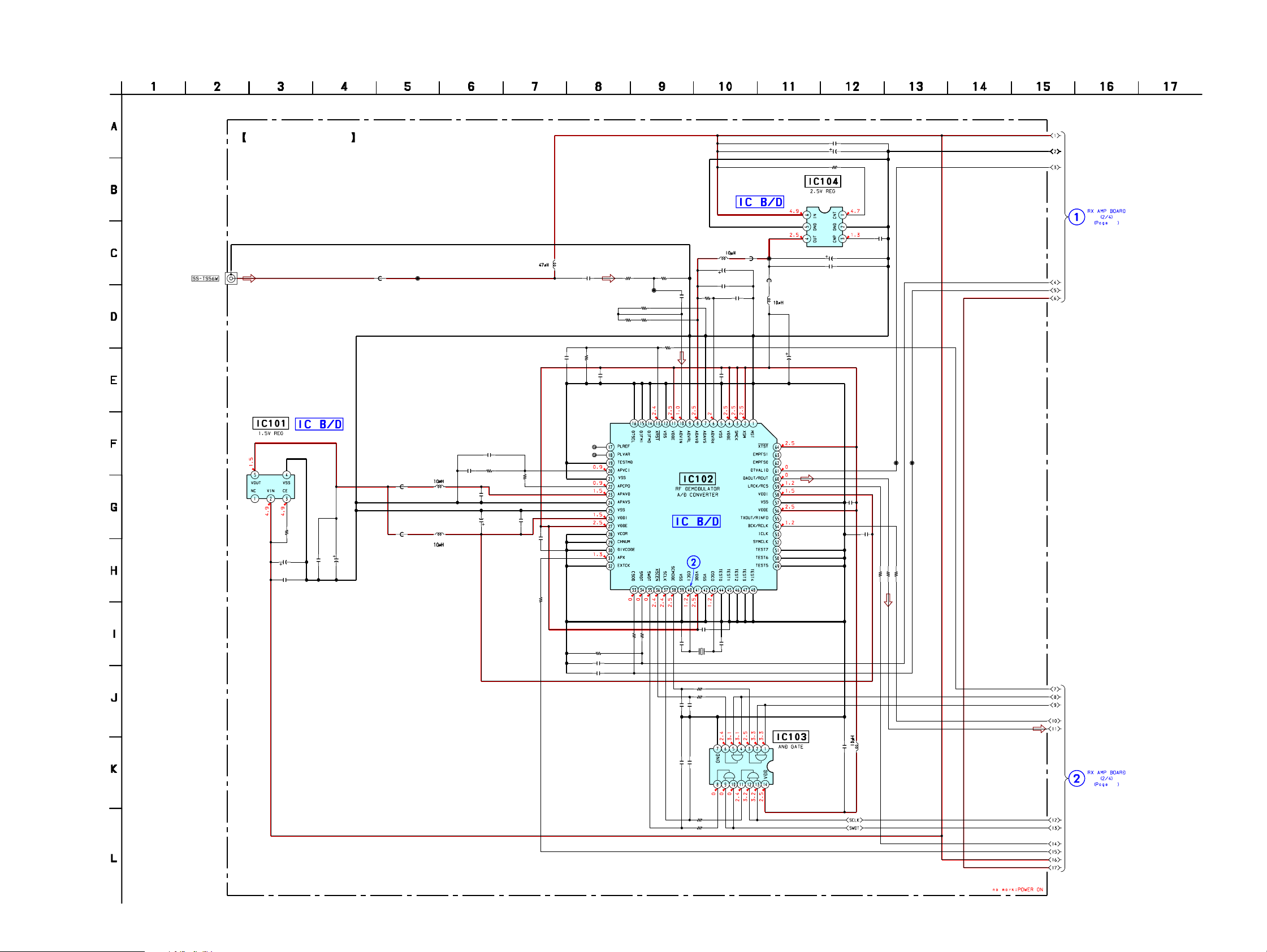
2-3. SCHEMATIC DIAGRAM — RX AMP BOARD (1/4) —
RX AMP BOARD (1/4)
J310
1P
FB109
• See page 4 for Waveform. • See page 13 for IC Block Diagrams.
L304
R324
R311
0UH
TP1
C317
0.01
C327
R322
0.1
3.3k
0
R312
R313 R314
2.2k 4.7k
C328
0.1
220
TP2
C329
0.01
4.7k
R323
C346
0.1
C345
10 50V
R330
10k
IC104
TK11225CMCL-G
8
0.01
L307
C336
47 16V
FB104
R329
C340
68
1
C339
1k
C338
0.1
0UH
L308
1
C344
47 16V
C343
0.1
C348
10
50V
FB103
0UH 0.2A
C350
IC101
XC62HR1502MR
10 50V
C313
C322
0.01
R318
820
L305
FB101
0UH
R317
10k
C314
0.1
16V
C316
47
C315
0.1
FB102
0UH
C321
0.1
C319
0.1
C318
47
16V
L306
R319
3.3k
C320
0.1
0.1
C324
330
R341
TP3
TP4
TP28
TP27
IC102
CXD4017R
R321
100
R320
47k
C326
0.001
C325
0.001
100
R342
C335
0.1
C337
27p
C332
27p
100p
C330
X101
12.288MHz
R328
100
R327
100
C334C331
100p100p
100p
C333
IC103
SN74LV08APWR
C342
1
0.1
C349
1k
1k
1k
R333
R332
R331
0.1
C341
L309
8
TA-WR4
R326
100
R325
100
77
TA-WR4
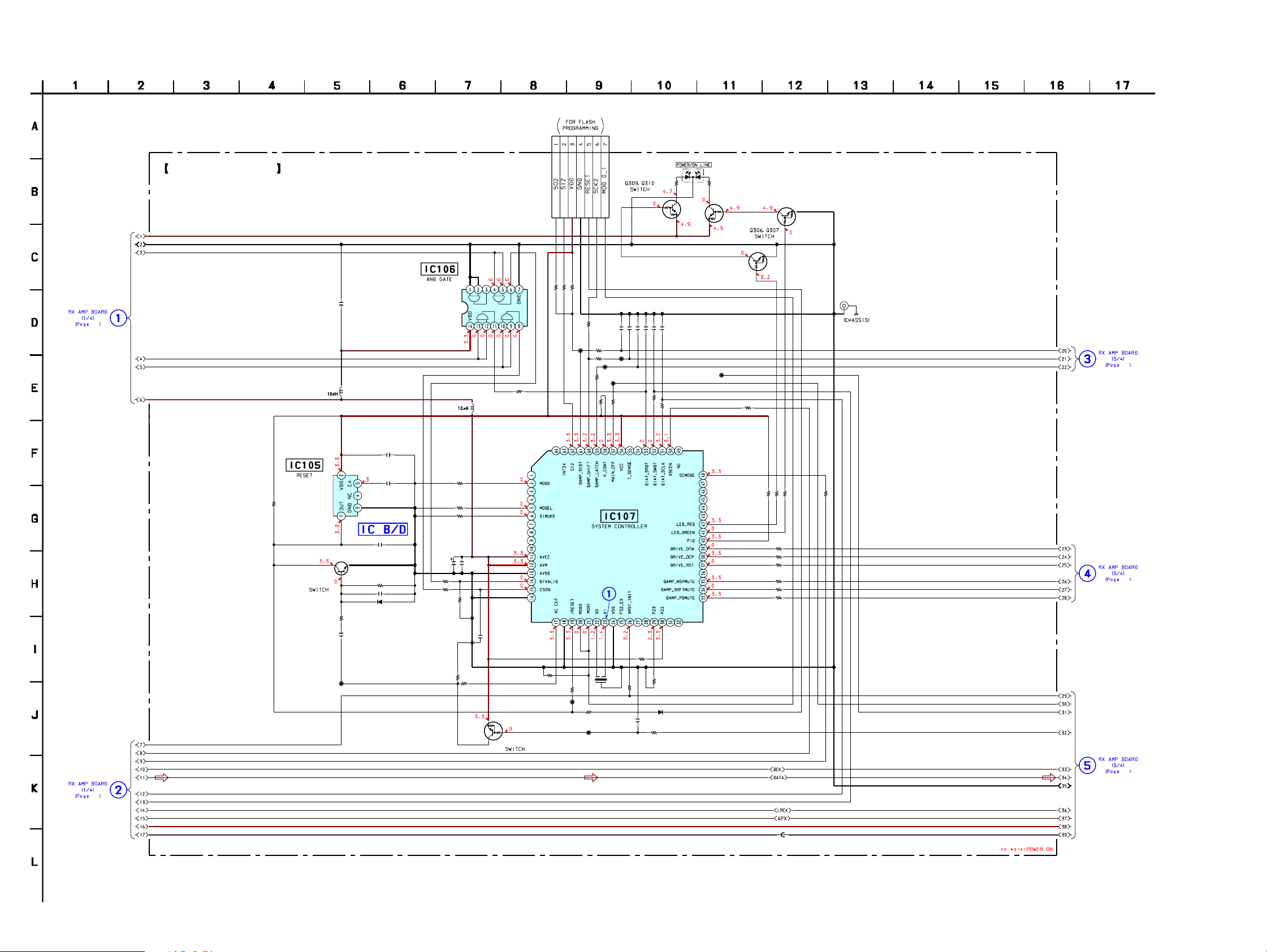
2-4. SCHEMATIC DIAGRAM — RX AMP BOARD (2/4) —
RX AMP BOARD (2/4)
7
• See page 4 for Waveform. • See page 13 for IC Block Diagram. • See page 17 for IC Pin Function Description.
CN303
7P
R316
150
Q309
DTA114EKA-
T146
3.3k
100
100
R379
R345
C358
0.1
L310
IC106
SN74LVC08APWR
R358
L311
R347
R349
100
R353
100
TP5
R352
100
TP7
100
R355
0
TP9
10k
R350
R372
100p
100p
10p
C364
TP6
1k
100p
100p
100p
C367
C368
C365
C370
C363
100
R360
R359
D100
SPR-54MVW
R338
150
Q310
DTA114EKA-
T146
Q306
DTC114EKA-
T146
TP8
100
R356
100
Q307
DTC114EKA-
T146
EARTH PLATE
EB102
9
R335
C355
0.1
47k
R340
C354
C357
0.1
R337
C356
D303
1SS355WTE-17
0.001
0.22
47k
R339
R354
47k
R380
47k
R381
IC107
MB89537APFM -G-1018E1
C360
C359
100
0.1
10V
1k
100
R399
47k
100p
C366
R373
47k
R367
100
Q308
DTA114EKA-
T146
R346
47k
R344
X102
100
TP29
100
R348
TP17
8MHz
R376
10k
R377
47k
R357
100
D304
1SS355TE-17
C395
0.22
R382
1k
Q305
2SC1623-T1
-L5L6
PST3629NR
IC105
TP30
R336
22k
C351
0.1
10k
10k
100
100
R378
R364
R365
100
R383
100
R384
100
R385
R363
100
R362
100
R361
100
100
R366
9
9
TA-WR4
7
FB105
0UH
88
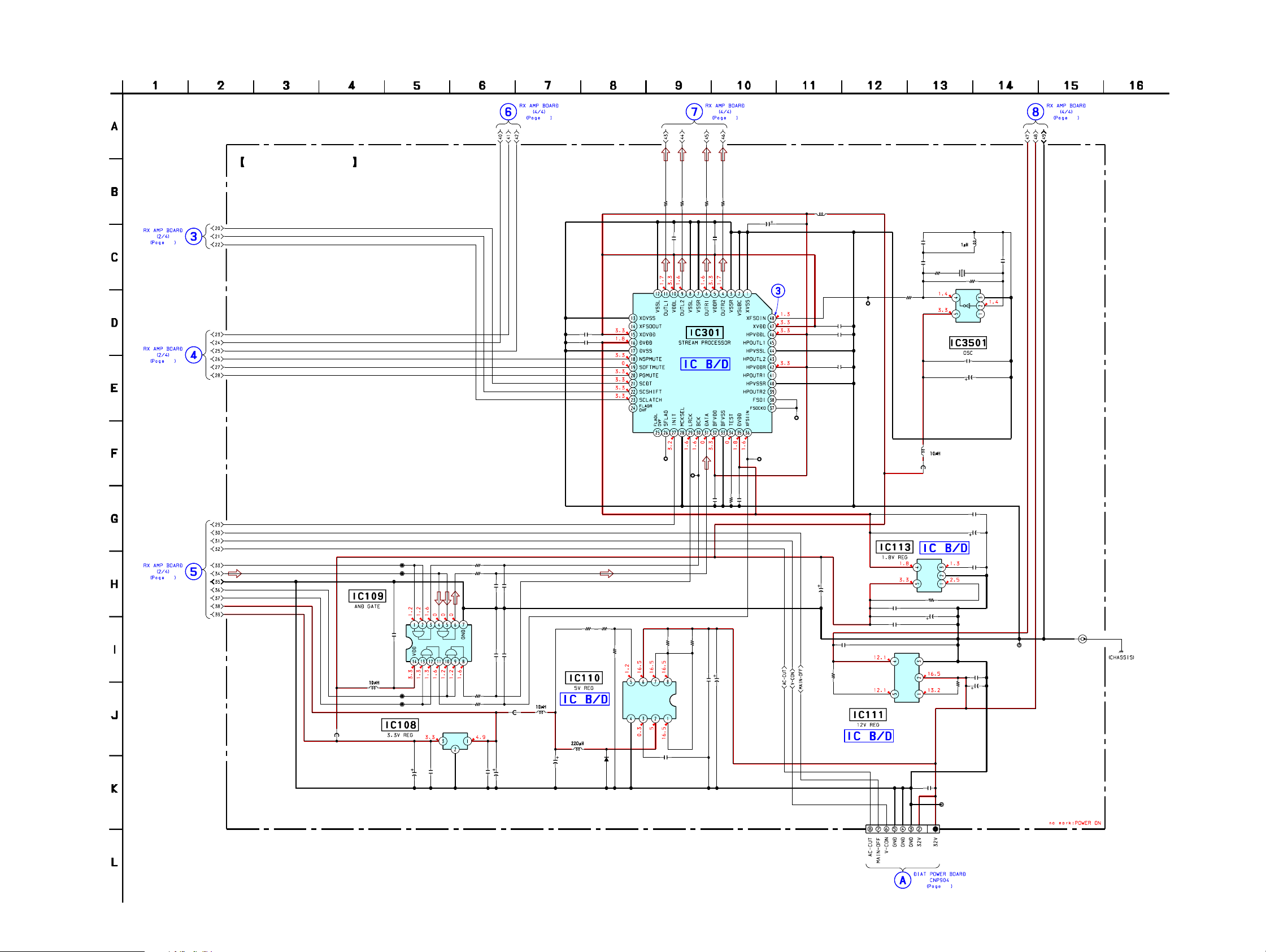
2-5. SCHEMATIC DIAGRAM — RX AMP BOARD (3/4) —
TA-WR4
Ver. 1.1
• See page 4 for Waveform. • See page 14 for IC Block Diagrams.
1010
10
RX AMP BOARD (3/4)
R202R201R102R101
100100100100
L3055
47 1 6 V
C401
8
0.1
C404
C405
0.1
8
C403 C402
0.1
0.1
IC301
CXD9876R
TP3015
0
R3053
100
L3054C418
X3051
49.152MHz
R3052
IC3051
SN74AHC1GU04DCKR
C415
0.01
C414
220 10V
C416C417
5p0.001
1M
5p
22
TP3056
0.1
C413
0.1
C412
0.1
C411
R3054
0.01
0.1
R374
C388
IC111
SI-3120KM-TL
L3053
FB3051
100k
100 10V
0
C383
0.01
C389
100
16V
C391
0.01
EB101
EARTH PLATE
TP23
C384
0.1
C386R397
47k
C392
0.1
TP24
100
35V
TP3014
TP3012
TP3013
TP18
8
FB106
0UH
TP19
C375
0.1
16V
L312
TP20
TP21
NJM2885DL1
-33(TE2)
C371
100
16V
C369 C372
0.01 0.01
IC108
R371
R370
R369
R368
IC109
100
100
C377 C379
100p 100p
100p
100p
SN74LVC08APWR
C376
C378
100
100
FB107
C373
100
35V
R387R386
1.5k1.5k
R388
1k
L313
0UH
L314
C409
470
10V
D306
11EQS04
-TA2B
R389 R390
11
IC110
(TE2)
NJM2374AE
C311
220p
0
0.1
0.1
C406
C407
R3016
16V
100
C380
C382
0.1
C410
C381
0.1
100
35V
R395
0
CN106
IC113
TK11118CSCL-G
C390
C387
8P
TA-WR4
12
99
 Loading...