Sony TAWR-2 Service manual
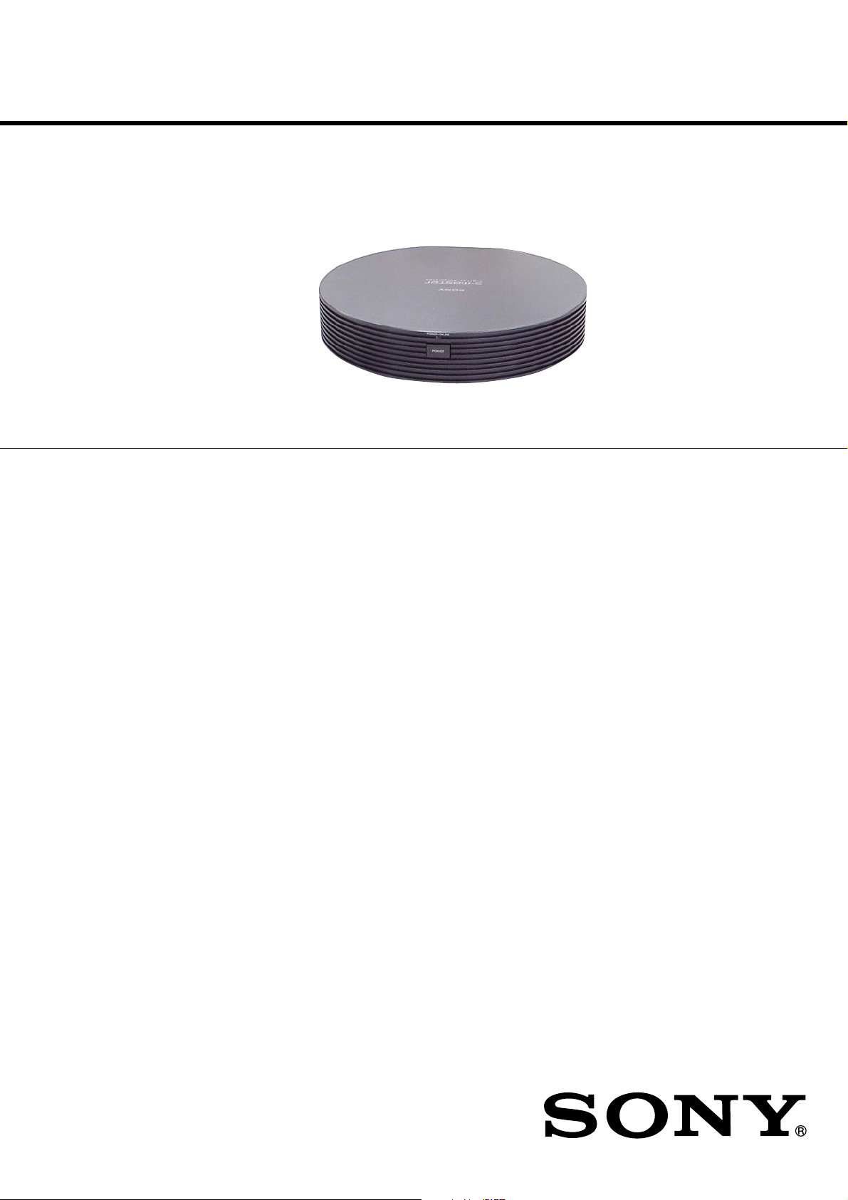
TA-WR2
SERVICE MANUAL
Ver. 1.2 2005.08
TA-WR2 is the surround amplifier section in
DAV-DZ700FW/DZ770W/FX100W/FX999W/FX1000W.
SPECIFICATIONS
Power requirements
US/Canadian/Mexican models 120V AC, 60Hz
Central/South American models 110-240V AC, 50/60Hz
Other models 220-240V AC, 50/60Hz
Power consumption 50 W
Dimensions (approx.) 260 260.5 58 mm
Mass (approx.) 1.45 kg
× ×
(w/h/d)
US Model
Canadian Model
AEP Model
UK Model
E Model
Australian Model
:
:
:
Design and specifications are subject to change
without notice.
9-879-677-03
2005H16-1
© 2005.08
SURROUND AMPLIFIER
Sony Corporation
Audio Group
Published by Sony Engineering Corporation
TA-WR2
r
Notes on chip component replacement
• Never reuse a disconnected chip component.
• Notice that the minus side of a tantalum capacitor may be
damaged by heat.
Flexible Circuit Board Repairing
• Keep the temperature of the soldering iron around 270 °C
during repairing.
• Do not touch the soldering iron on the same conductor of the
circuit board (within 3 times).
• Be careful not to apply force on the conductor when soldering
or unsoldering.
UNLEADED SOLDER
Boards requiring use of unleaded solder are printed with the leadfree mark (LF) indicating the solder contains no lead.
(Caution: Some printed circuit boards may not come printed with
the lead free mark due to their particular size)
: LEAD FREE MARK
Unleaded solder has the following characteristics.
• Unleaded solder melts at a temperature about 40 °C higher
than ordinary solder.
Ordinary soldering irons can be used but the iron tip has to be
applied to the solder joint for a slightly longer time.
Soldering irons using a temperature regulator should be set to
about 350 °C.
Caution: The printed pattern (copper foil) may peel away if
the heated tip is applied for too long, so be careful!
• Strong viscosity
Unleaded solder is more viscou-s (sticky, less prone to flow)
than ordinary solder so use caution not to let solder bridges
occur such as on IC pins, etc.
• Usable with ordinary solder
It is best to use only unleaded solder but unleaded solder may
also be added to ordinary solder.
SAFETY CHECK-OUT
After correcting the original service problem, perform the following
safety check before releasing the set to the customer:
Check the antenna terminals, metal trim, “metallized” knobs, screws,
and all other exposed metal parts for AC leakage.
Check leakage as described below.
LEAKAGE TEST
The AC leakage from any exposed metal part to earth ground and
from all exposed metal parts to any exposed metal part having a
return to chassis, must not exceed 0.5 mA (500 microamperes.).
Leakage current can be measured by any one of three methods.
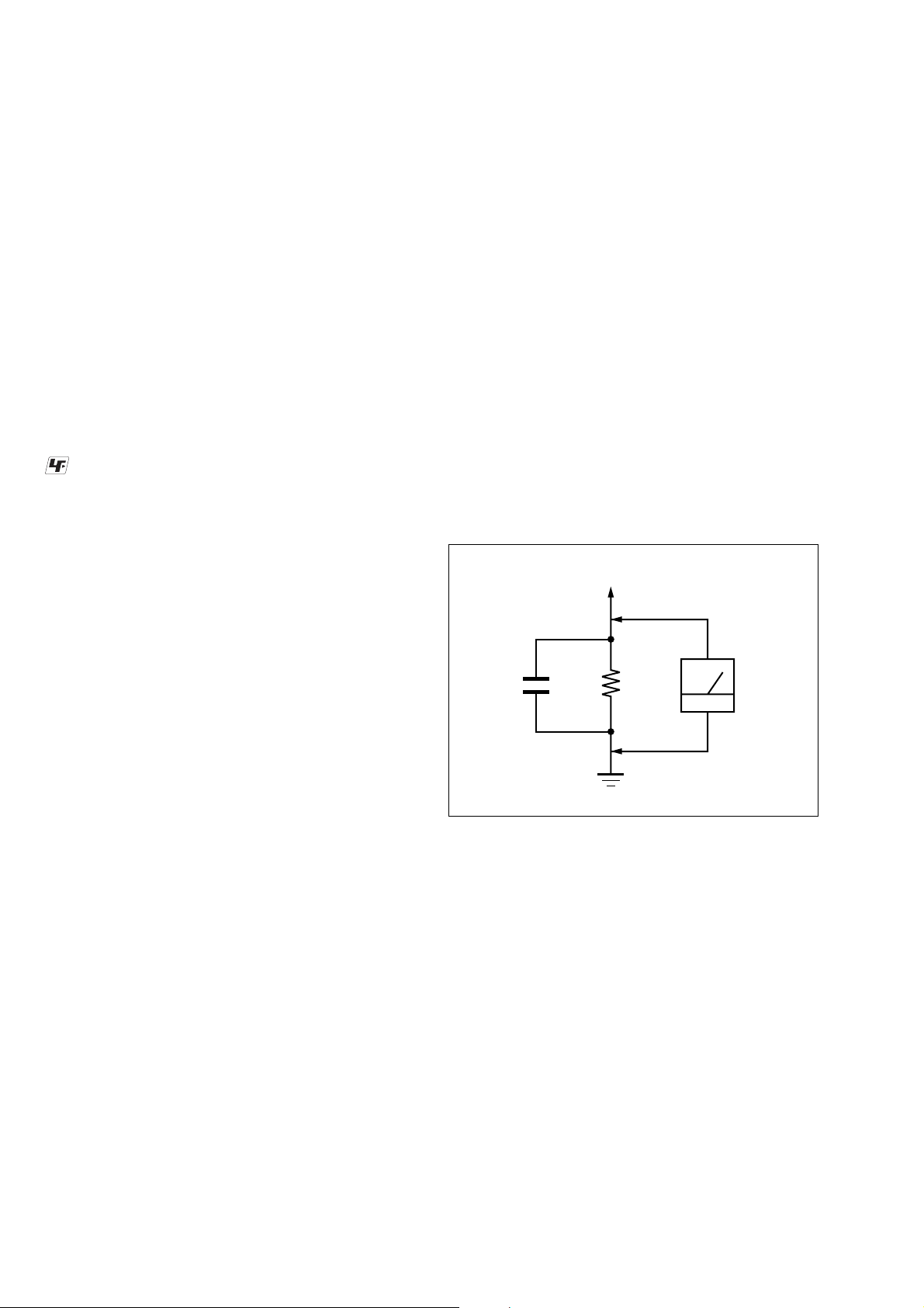
1. A commercial leakage tester, such as the Simpson 229 or RCA
WT -540A. Follow the manuf acturers’ instructions to use these
instruments.
2. A battery-operated A C milliammeter . The Data Precision 245
digital multimeter is suitable for this job.
3. Measuring the voltage drop across a resistor by means of a
VOM or battery-operated AC v oltmeter. The “limit” indication
is 0.75 V, so analog meters must have an accurate low-v oltage
scale. The Simpson 250 and Sanwa SH-63Trd are examples
of a passive VOM that is suitable. Nearly all battery operated
digital multimeters that have a 2 V A C range are suitable. (See
Fig. A)
To Exposed Metal
Parts on Set
AC
0.15 µF
1.5 k
Ω
voltmete
(0.75 V)
SAFETY-RELATED COMPONENT WARNING!!
COMPONENTS IDENTIFIED BY MARK 0 OR DOTTED LINE
WITH MARK 0 ON THE SCHEMATIC DIAGRAMS AND IN
THE PARTS LIST ARE CRITICAL TO SAFE OPERATION.
REPLACE THESE COMPONENTS WITH SONY PARTS WHOSE
PART NUMBERS APPEAR AS SHOWN IN THIS MANUAL OR
IN SUPPLEMENTS PUBLISHED BY SONY.
ATTENTION AU COMPOSANT AYANT RAPPORT
À LA SÉCURITÉ!
LES COMPOSANTS IDENTIFIÉS PAR UNE MARQUE 0 SUR
LES DIAGRAMMES SCHÉMATIQUES ET LA LISTE DES
PIÈCES SONT CRITIQUES POUR LA SÉCURITÉ DE
FONCTIONNEMENT. NE REMPLACER CES COM- POSANTS
QUE PAR DES PIÈCES SONY DONT LES NUMÉROS SONT
DONNÉS DANS CE MANUEL OU D ANS LES SUPPLÉMENTS
PUBLIÉS PAR SONY.
Earth Ground
Fig. A. Using an AC voltmeter to check AC leakage.
TABLE OF CONTENTS
1. GENERAL ................................................................... 3
2. DIAGRAMS
2-1. Block Diagram ................................................................ 5
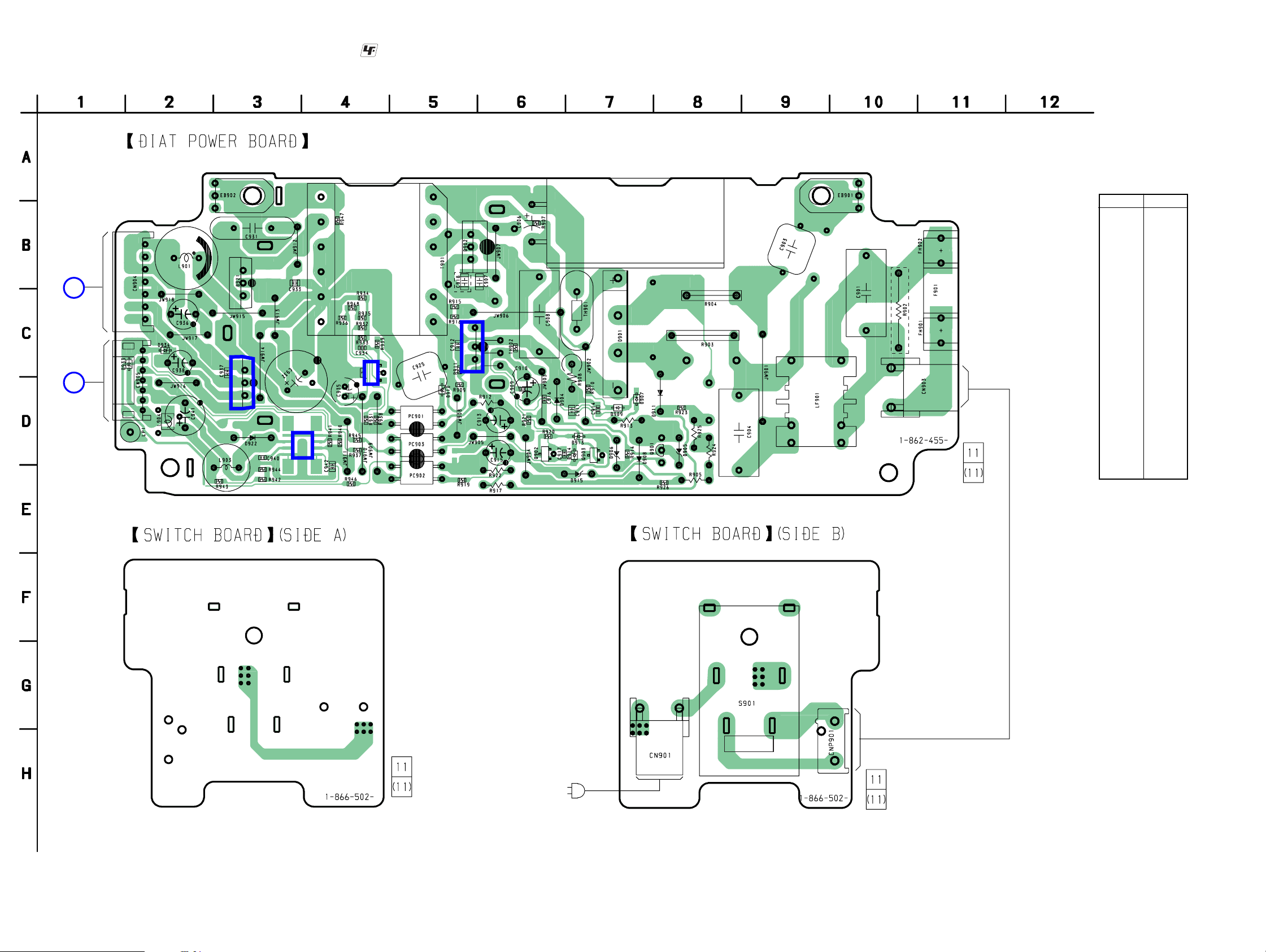
2-2. Printed Wiring Board — DIAT POWER Section —...... 6
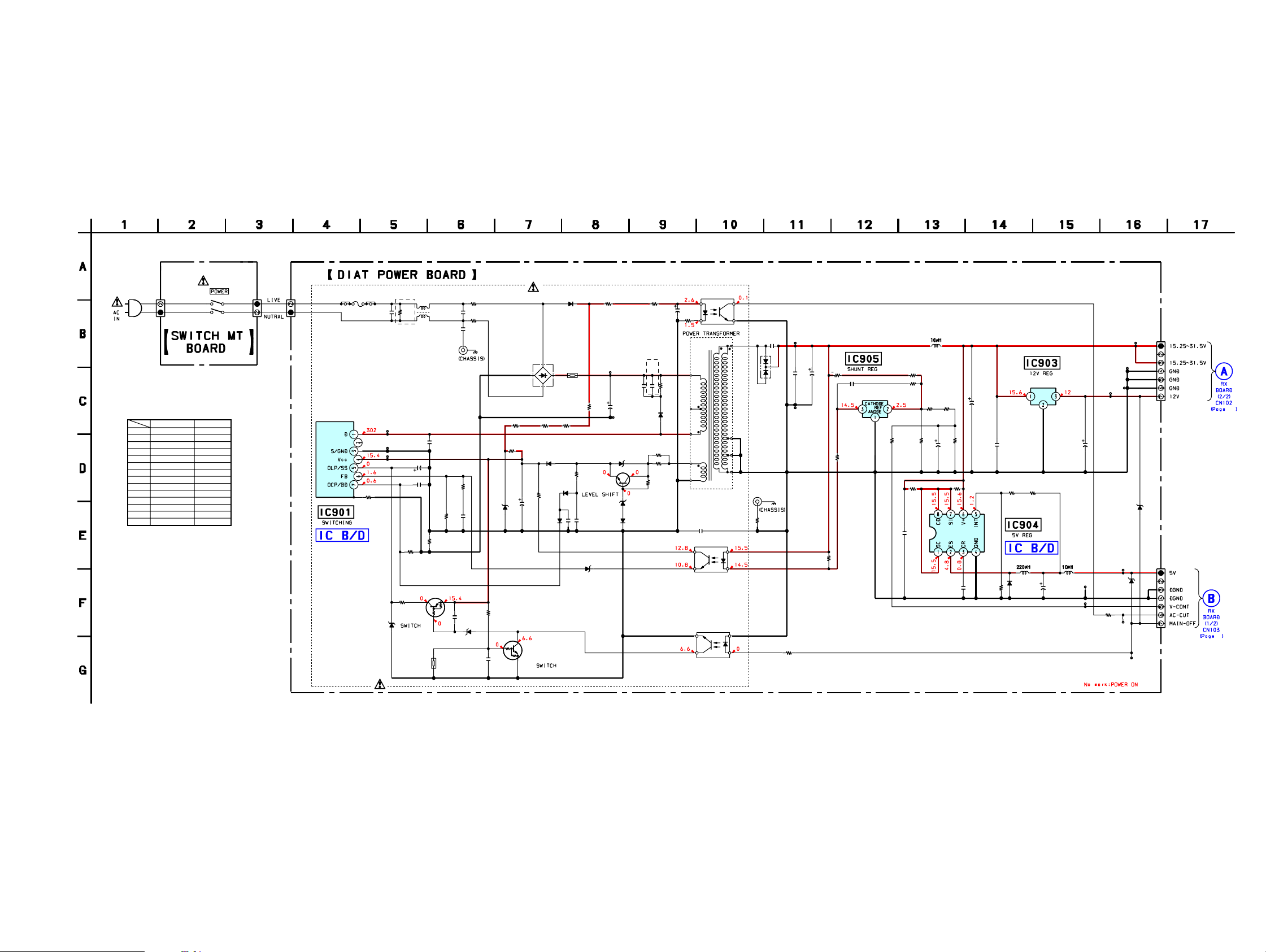
2-3. Schematic Diagram — DIAT POWER Section — ........ 7
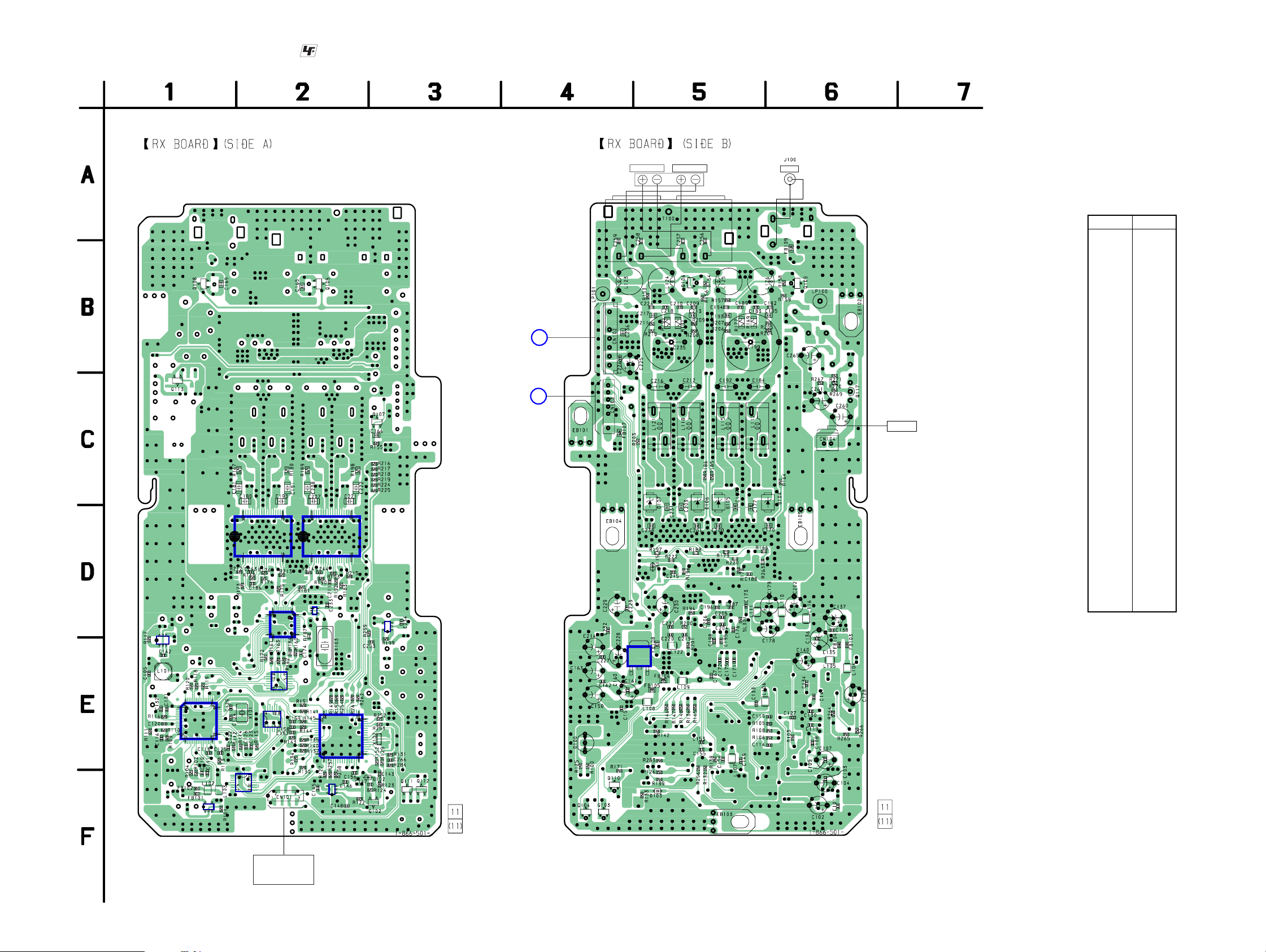
2-4. Printed Wiring Board — RX Board — .......................... 8
2-5. Schematic Diagram — RX Board (1/2) — .................... 9
2-6. Schematic Diagram — RX Board (2/2) — .................... 10
3. EXPLODED VIEWS
3-1. Overall Section ................................................................ 17
3-2. RX Board, DIAT POWER Board Section ....................... 18
4. ELECTRICAL PARTS LIST .................................. 19
2
Surround amplifier
SECTION 1
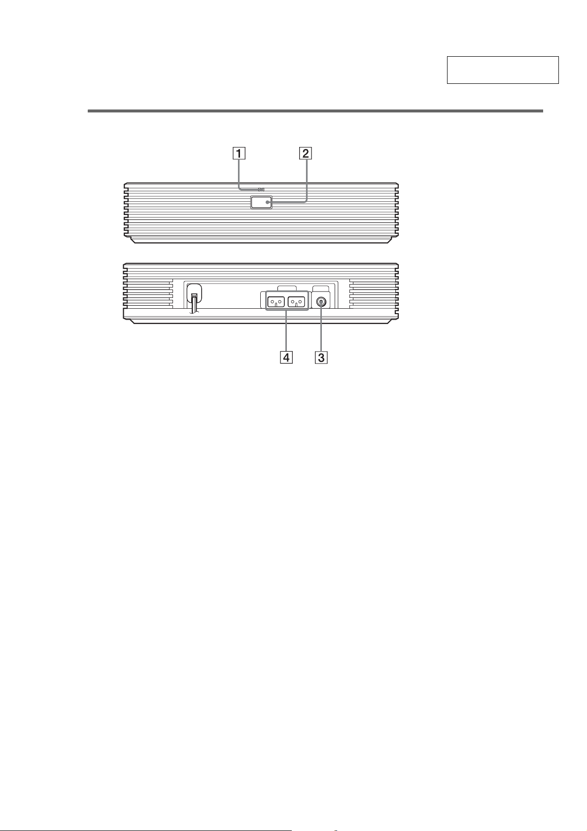
GENERAL
POWER/ON LINE
POWER
TA-WR2
This section is extracted
from instruction manual.
Front panel
A POWER/ON LINE indicator (33)
B POWER (33)
SPEAKER DIR-R2
SURROUND L SURROUND R
Rear panel
C DIR-R2 jack (15)
D SPEAKER jacks (15)
3
TA-WR2
SECTION 2
DIAGRAMS
• Note for Printed Wiring Boards and Schematic Diagrams
Note on Printed Wiring Boards:
• X : parts extracted from the component side.
• Y : parts extracted from the conductor side.
• f : internal component.
• : Pattern from the side which enables seeing.
(The other layers' patterns are not indicated.)
Caution:
Pattern face side: Parts on the pattern face side seen from
(SIDE A) the pattern face are indicated.
Parts face side: Parts on the parts face side seen from
(SIDE B) the parts face are indicated.
• Indication of transistor.
C
Q
B
E
B
These are omitted.
Q
CE
These are omitted.
Note on Schematic Diagrams:
• All capacitors are in µF unless otherwise noted. (p: pF)
50 WV or less are not indicated except f or electrolytics and
tantalums.
• All resistors are in Ω and 1/
specified.
• f : internal component.
• 2 : nonflammable resistor.
• C : panel designation.
Note:
The components identified by mark 0 or dotted line with mark 0 are
critical for safety.
Replace only with part
number specified.
• A : B+ Line.
•Voltages and waveforms are dc with respect to ground
under no-signal (detuned) conditions.
no mark: Power on
•Voltages are taken with a VOM (Input impedance 10 MΩ).
Voltage variations may be noted due to normal production
tolerances.
•Waveforms are taken with a oscilloscope.
Voltage variations may be noted due to normal production
tolerances.
• Circled numbers refer to waveforms.
• Signal path.
F : AUDIO
•Abbreviation
RU : Russian model
CND : Canadian model
4
W or less unless otherwise
Note:
Les composants identifiés
par une marque 0 sont critiques pour la sécurité.
Ne les remplacer que par une
piéce portant le numéro
spécifié.
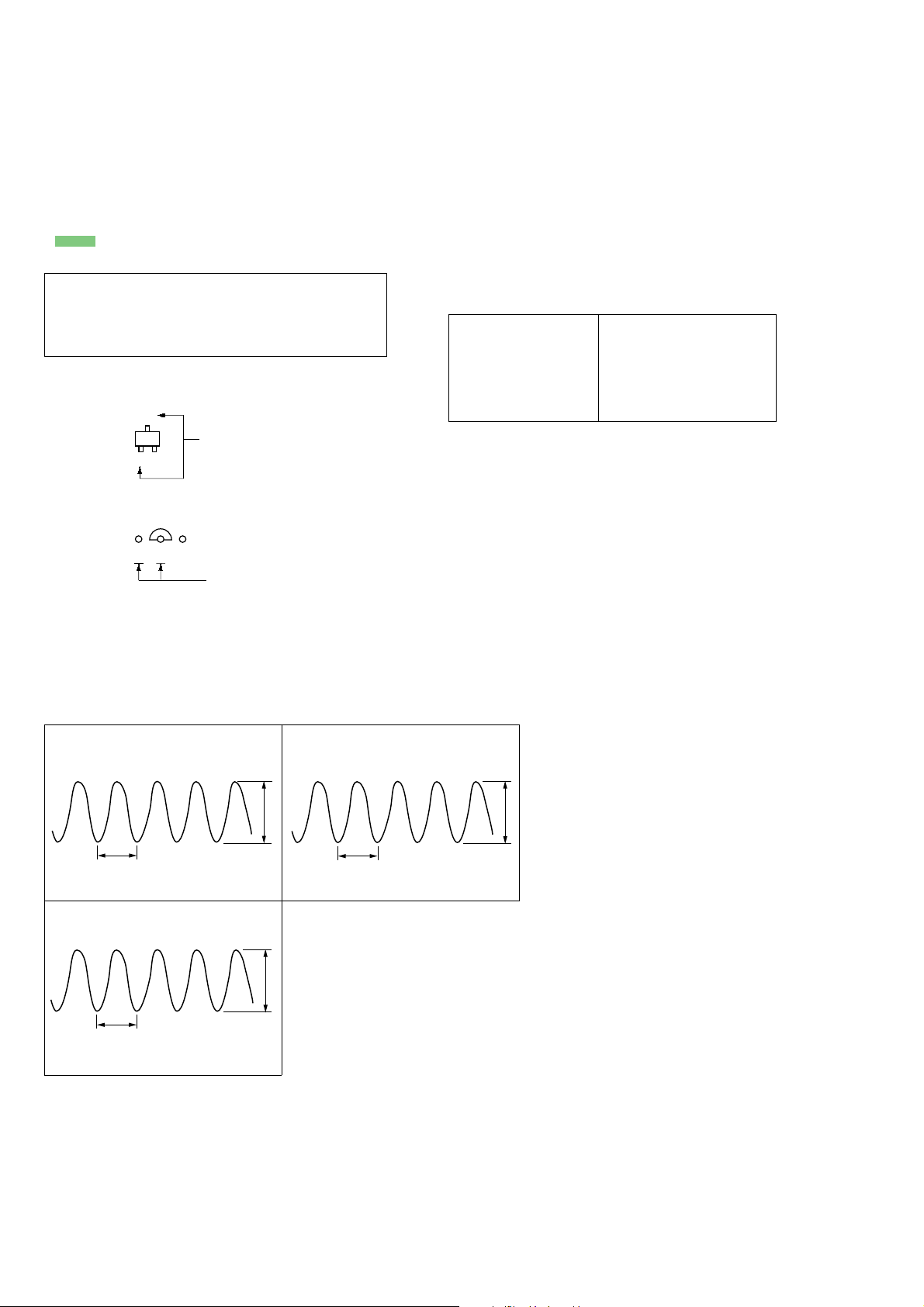
•Waveforms
– RX Board –
1
IC107 wd (X1)
1 V/DIV, 100 ns/DIV
2
IC102 r; (OSCI)
1 V/DIV, 40 ns/DIV
125 ns
81.3 ns
3.7 Vp-p
3.4 Vp-p
3
IC111 rk (XFSOIN)
20.3 ns
1 V/DIV, 10 ns/DIV
4.8 Vp-p
4
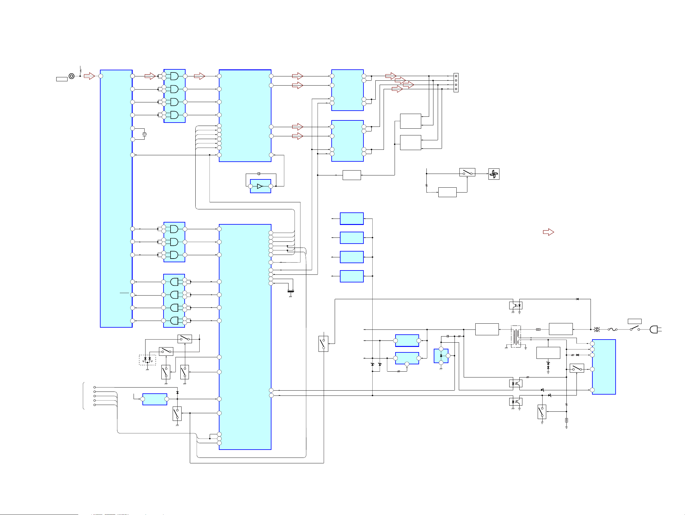
2-1. BLOCK DIAGRAM
TA-WR2
J100
DIR-R2
5V
L101
RF DEMODULATOR
A/D CONVERTER
10
ADVIN
IC102
DAOUT
BCK
APX
LRCK
OSCI
OSCO
XRST
DTVALID
CSOB
SRDT
SCMODE
XSCEN
SCLK
SWDT
31
60
54
31
59
40
43
13
31
61
33
34
31
38
36
37
35
D100
DATA
BCK
APX
LRCK
GREEN
X101
12.288MHz
RED
Q103
11
12
13
10
10
12
13
3
6
8
4
5
1
2
9
4
5
9
Q111
IC109
AND GATE
IC106
AND GATE
IC103
AND GATE
6
3
11
8
6
8
11
1
2
4
5
9
10
12
13
Q112 5V
Q104
SCLK
SWDT
31
DATA
30
BCK
36
XFSIIN
29
LRCK
18
NSPMUTE
19
SOFTMUTE
20
PGMUTE
21
SCDT
22
SCSHIFT
23
SCLATCH
27
INIT
14
DRVALID
15
CSOD
53
DIAT_SRDT
48
SCMODE
50
XSCEN
51
DIAT SCLK
52
DIAT SWDT
42
LED RED
41
LED GREEN
IC111
STREAM PROCESSOR
49.152MH
2 4
IC107
SYSTEM CONTROLLER
DAMP_NSPMUTE
DAMP_SOFTMUTE
DAMP_SGMUTE
DAMP_SCDT
DAMP_SHIFT
DAMP_LATCH
XRST_INIT
DRIVE RST
DRIVE OCP
XFSOIN
X103
IC114
OSC
OUTL1
OUTL2
OUTR1
OUTR2
IC110
POWER AMP
3.3V
3.3V
2.5V
1.8V
1.5V
2
17
4
13
2
17
4
13
PWMBP
PWMAP
/RST
/SD
POWER AMP
PWMBP
PWMAP
/RST
/SD
AC CUT
IC112
11
9
6
4
48
Z
35
34
33
61
60
59
26
37
38
22
XO
23
XI
X102
8MHZ
(1)
(2)
Q110
OUT B
OUT B
OUT A
OUT A
OUT B
OUT B
OUT A
OUT A
Q107
PRO TECT
IC108
3.3V REG
IC104
2.5V REG
IC113
1.8V REG
IC101
1.5V REG
30
29
26
25
Q108,109
OVER LOAD
30
29
26
25
DETECT
Q105,106
OVER LOAD
DETECT
12V
30V
12V
5V
IC903
13
12V REG
IC904
5V REG
5
6
SHUNT REG
2
IC905
Q113
SWITCH
3
1
T100
REAR RCH+
REAR RCHREAR LCH+
REAR LCH-
Q117 DC FAN
2
D921
RECT
• Signal Path
PC902 D911
T901
POWER TRANSFORMER
PC901
TH901
Q901
LEVEL SHIFT
: AUDIO
D901
MAIN RECT
Q902
LF901
SWITCHING
1
D
4
VCC
7
OCP/BD
5
SS/OLP
IC901
F901
*
T3.15A/250V(AEP, UK, RU)
S901
POWER
*F901
T5A/125V(US, CND)
AC IN
TA-WR2
FLASH
PROGRAMING
CONNECTOR
RESET
SCK2
SO2
MOD
(1)
(2)
(3)
(4)
SI2
3.3V
2 1
VDD
OUT
IC105
RESET
Q102
19
/RESET
17
AC CUT
21
(3)
(4)
MOD1
20
MOD0
62
SI2
V CONT
MAIN OFF
58
57
V CONT
MAIN OFF
PC903
Q903
TH902
6
FB
55
TA-WR2
2-2. PRINTED WIRING BOARD — DIAT POWER SECTION —
1
A
RX BOARD
CN102
(Page 8)
B
RX BOARD
CN103
(Page 8)
7
7
1
IC903
1
2
3
IC905
IC904
1
8
45
:Uses unleaded solder.
AEP, UK, RU
1
IC901
3
1
K
AC
K
AC
C
E
6
E
E
A
K
• Semiconductor
Location
Ref. No.
D901 C-7
D902 B-5
D904 D-6
D905 D-8
AEP, UK, RU
D906 D-7
D907 D-7
D908 D-7
D909 D-7
D910 D-5
D911 D-8
D913 D-7
3
D914 D-7
D915 E-7
D921 B-3
D922 D-3
7
D933 C-2
D934 C-2
IC901 C-5
IC903 C-3
IC904 D-3
IC905 C-4
Q901 D-8
EE
E
Q902 D-6
Q903 D-7
Location
TA-WR2
POWER
AC IN
66
TA-WR2
2-3. SCHEMATIC DIAGRAM — DIAT POWER SECTION —
*
C903
C906
C907
C908
IC901
LF901
R905
R906
R908
R917
R922
R924
R925
T901
CN901
2P
US, CND AEP, UK, RU
0.0022uF, 250V
330uF, 200V
10000PF, 630V
3300PF, 1.2KV
STR-W6735N
1-424-930-11
15k, 1/4W
100k, 2W
0.12, 2W
33k, 1/4W
33k, 1/4W
15k, 1/4W
15k, 1/4W
1-443-744-11
3300PF, 630V
680PF, 1.5KV
STR-W6765N
1-457-083-11
1-443-743-11
440PF, 250V
100uF, 450V
22k, 1/4W
82k, 2W
0.27, 2W
47k, 1/4W
47k, 1/4W
22k, 1/4W
22k, 1/4W
S901
CNP901
2P
CN903
2P
F901
T3.15AL/
250V
FH901 FH902
IC901
*
R907
UDZSTE-176.2B
D913
C901
0.22
275V
0
• See page 11 for IC Block Diagrams.
AEP, UK, RU
TP914
D
TP915
S/GND
TP916
R920
4.7k
DTA114EKA-T146
R902
1M
1/2W
VCC
R910
100
Q902
(POSITIVE)
TH902
LF901
43MH
0.6A
LFC
*
C908
C909
50V
C910
470p
50V
R909
R908
R903
JW
C904
R904
0.1
JW
275V
C903
*
EB901
*
10
R911
1k
C912
0.1
1k
50V
*
C917
0.01
D914
UDZSTE-1710B
C916
0.01
R926
R921
10k
68k
R905
33B
D915
MTZJ-T-77-
D901
D3SB60F3
*
R924
11EQS10-TE1
1SS355TE-17
R912
1k
C913
1/4W
22
50V
Q903
DTC144EKA-T146
D911 PC902
R923
0
2SD1616A-TP-LK
C911
100p
100V
D910
UDZSTE-179.1B
C906
Q901
R917
*
TP912
VIN
*
TP913
GND
MTZJ-T-77-33B
D905
C907
*
MTZJ-T-77-20B
11EQS10-TA1
*
D908
D907
D909
10EDB60-TA1B2
TH901
NTC8.0
R925
R913
820
1/4W
1SS355TE-17
C914
0.0033
50V
*
AEP, UK, RU
C918
3300p
630V
D902
SARS03
D906
D904
R922
R914
4.7k
R919
1.5k
PC123Y22JO0F
T901
C925
0.001
250V
PC901
PC123Y22JO0F
PC903
PC123Y22JO0F
*
EB902
D921
FML-22S
R947
4700p
0
C931
TP910
VOUT
1kV
R931
27k
+0.5%
C932
1000
C933
35V
0.1
50V
TP911
GND
R945
2.2k
R938
C934
IC905
0.01
NJM1431AU
R937
390
R939
1k
1k
R934
4.7k
R933
R940
C942
L901
R932
0
47k
R948
R935
330
3.9k
R936
C935
2.2k
100
16V
1
0.1
50V
C936
100
35V
C937
0.1
50V
1
R941
IC904
NJM2374AE(TE2)
C940
220p
50V
R944
1k
IC903
TA7812S
C938
100
16V
R942
R943
1.5k1.5k
UDZSTE-1710B
L903
D922
11EQS04
-TA1B
L904
C941
470
10V
TP906
DGND
TP907
V-CONT
TP905
UDZSTE-1710B
R946
100
TP903
TP904
D933
12V
5V
TP902
GND
D934
GND
TP908
AC-CUT
TP901
CN904
7P
30V
10
CN905
7P
9
TP909
MAIN-OFF
*
C915
47
35V
R906
*
R916
22
R915
22
TA-WR2
77
TA-WR2
2-4. PRINTED WIRING BOARD — RX BOARD —
E
E
:Uses unleaded solder.
E
E
A
DIAT POWER
BOARD
CN904
(Page 6)
B
DIAT POWER
BOARD
CN905
(Page 6)
SURROUND L
SURROUND R
DIR-R2
• Semiconductor
Location
Ref. No.
D100 E-4
D102 F-3
D103 F-5
E
E
D104 C-6
D105 C-5
D106 C-5
D107 C-5
1
D115 D-5
IC101 F-1
IC102 E-1
IC103 E-2
6
6
E
IC104 E-1
IC105 F-2
IC106 F-2
IC107 E-2
IC108 E-5
IC109 E-2
1
DC FAN
IC110 D-2
IC111 D-2
IC112 D-2
IC113 D-3
IC114 D-2
Location
46
13
IC104
IC102
1
IC101
IC110
4
5
3
IC111
IC109
IC106
IC103
1
3
5
4
IC114
IC107
4
5
3
IC105
1
IC112
IC113
E
Q102 F-3
Q103 F-4
Q104 F-4
Q105 B-2
Q106 B-5
Q107 C-3
Q108 B-1
Q109 B-6
Q110 F-4
Q111 F-3
Q112 F-3
Q113 C-1
Q117 C-6
4
3
5
1
EE
IC108
13
E
E
E
TA-WR2
FLASH
PROGRAMMING
CONNECTOR
88
 Loading...