

Sony TAVE-170 Service manual

TA-VE170
SERVICE MANUAL
• This set is the Amplifier section in
HT-K170.
Manufactured under license from Dolby Laboratories
Licensing Corporation.
“DOLBY”, “AC-3”, “Pro Logic” and the double-D symbol
; and “Pro Logic” are trademarks of Dolby
Laboratories Licensing Corporation.
SPECIFICATIONS
AEP Model
UK Model
E Model
Australian Model
Chinese Model
Power output
Rated Power
Output at Stereo
mode
Reference
Power Output
Frequency
response
Inputs
Sensitivity
TV,
VIDEO,
DVD 2CH,
5.1 CH/
DVD
250 mV
(DIN 1 kHz, 8 ohms)
25 W + 25 W
(DIN 1 kHz, 8 ohms)
Front: 25 W / ch
Center: 25 W
Rear: 25 W / ch
TV, VIDEO, DVD 2CH,
5.1 CH/DVD :
10 Hz - 50 kHz +0.5/–2 dB
Impedance
50
kilohms
S/N
(weighting
network,
input level)
85
dB*
(A, 250 mV)
*78IHF
Outputs
Muting
General
Power
requirements
Power
consumption
Dimensions
Mass (Approx.)
Design and specifications are subject to
change without notice.
WOOFER:
Voltage: 1 V
Impedance: 1 kilohms
Full mute
220 - 230 V AC, 50/60 Hz
115 W
430 x 274 x 64.5 mm
4.6 kg
HOME THEATER SYSTEM

TABLE OF CONTENTS
1. GENERAL ········································································· 3
2. DISASSEMBLY ································································ 4
3. TEST MODE·····································································5
4. DIAGRAMS········································································6
4-1. Notes for Printed Wiring Board
and Schematic Diagram·················································· 6
4-2. Printed Wiring Board – MAIN Section – ······················ 9
4-3. Schematic Diagram – MAIN Section (1/2) – ·············· 10
4-4. Schematic Diagram – MAIN Section (2/2) – ·············· 11
4-5. Printed Wiring Boards – PANEL Section –················· 12
4-6. Schematic Diagram – PANEL Section – ····················· 13
4-7. Printed Wiring Boards – POWER Section – ··············· 14
4-8. Schematic Diagram – POWER Section –···················· 15
4-9. IC Pin Function Description ········································· 16
5. EXPLODED VIEWS····················································· 17
6. ELECTRICAL PARTS LIST·····································19
SAFETY-RELATED COMPONENT WARNING!!
COMPONENTS IDENTIFIED BY MARK 0 OR DOTTED LINE WITH
MARK 0 ON THE SCHEMATIC DIAGRAMS AND IN THE PARTS
LIST ARE CRITICAL TO SAFE OPERATION. REPLACE THESE
COMPONENTS WITH SONY PARTS WHOSE PART NUMBERS
APPEAR AS SHOWN IN THIS MANUAL OR IN SUPPLEMENTS
PUBLISHED BY SONY.
Flexible Circuit Board Repairing
• Keep the temperature of soldering iron around 270˚C
during repairing.
• Do not touch the soldering iron on the same conductor of the
circuit board (within 3 times).
• Be careful not to apply force on the conductor when soldering
or unsoldering.
2

1
1 ?/1 button
2 CENTER MODE button
3 VIDEO button
4 TV button
5 DVD 2CH button
6 5-1 CH/DVD button
7 SOUND FIELD button
8 MASTER VOLUME knob
2
SECTION 1
GENERAL
3 4
5 6 7 8
1 5.1 CH/DVD
2 DVD 2CH
3 TV
15 7
3
8642
4 VIDEO
5 WOOFER
6
FRONT SPEAKER
This section is extracted
from instruction manual.
9
7 REAR SPEAKERS
8 CENTER SPEAKER
9 Mains lead
3

s
)
SECTION 2
DISASSEMBLY
Note: Follow the disassembly procedure in the numerical order given.
CASE, FRONT PANEL SECTION
2
two tapping screws
6
flat wire
(CNS301)
4
case
3
screw (BVTP3 x8)
8
front panel section
MAIN BOARD
claw
6
connector
(CNS800)
7
four screws
(BVTP3 x8)
5
connector
(CNP802)
4
connector
(CNS801)
claw
1
two tapping screw
5
flat wire
(CNS302)
7
six screws
(BVTP3 x8)
8
Remove the
MAIN board
to direction of
the arrow
A
2
DC fan
A
1
two screws
(BVTP3 x8)
3
six screws
(BVTP3 x8
4

SECTION 3
TEST MODE
This equipment is provided with a test mode built in the microcomputer .
The contents are described in the following.
[Initial Mode]
1.
Press ?/1 button while pressing both [TV] and
buttons simultaneously.
2. “INITIAL” is displayed on the fluorescent indicator tube, and
the status of the unit is set in the following.
• All Memory is clear.
• Center, rear level set to 0.
• Center mode set to NORMAL.
• Muting clear.
• Volume level set to min.
• FAN is on.
[Factory Mode]
1.
Press
?/1
button while pressing three buttons of
[DVD2CH]
2. Factory setting same as initial except center mode set to normal
using jog can set to volume max or min directly.
[FL Check Mode]
1. Press
simultaneously.
2. Fluorescent indicator tube and LED are checked, “FINISH” is
displayed and the status of the unit is set back in normal condition.
, and
?/1
button while both
[5.1CH/DVD]
[
CENTERMODE
simultaneously.
[5.1CH/DVD]
[VIDEO]
]
and
[TV]
buttons
,
[Gain Up Mode]
1. Press
2. “NOMAL” is displayed on the fluorescent indicator tube and
3. T o exit from this mode, press tw o buttons in the same manner as
[Version Mode]
1.
2. V ersion of its destination is displayed on the fluorescent indicator
[FAN ON/OFF]
• Press
• “FAN ON” t fan always turn on.
• “F AN AUTO” t when micro computer detected enough input
?/1
button while pressing
the rear is gained up 3 dB.
step1.
“GAIN LOW” is displayed on the fluorescent indicator tube and
the status of the unit is set back in normal condition.
Press
?/1
button while pressing three buttons of
[
DVD2CH
tube.
signal fan turn on automatically. Normally fan is off.
]
and
[
SOUNDFIELD
?/1 button while pressing
[
SOUNDFIELD
]
button.
[CENTERMODE]
]
buttons simultaneously.
[CENTERMODE]
button.
,
5

SECTION 4
d
B
These are omitted.
CE
Q
DIAGRAMS
• Circuit Boards Location
SECONDARY board
PW.SW borad
PRIMARY board
STANDBY board
MAIN boar
DISPLAY board
JOG board
4-1. NOTES FOR PRINTED WIRING BOARD AND SCHEMATIC DIAGRAM
Note on Schematic Diagram:
• All capacitors are in µF unless otherwise noted. pF: µµF
50 WV or less are not indicated except for electrolytics
and tantalums.
• All resistors are in Ω and 1/
specified.
¢
•
• 2 : nonflammable resistor.
• C : panel designation.
• U : B+ Line.
• V : B– Line.
• Voltages and waveforms are dc with respect to ground
• V oltages are taken with a V OM (Input impedance 10 MΩ).
• Waveforms are taken with a oscilloscope.
• Circled numbers refer to waveforms.
• Signal path.
: internal component.
Note:
The components identified
by mark 0 or dotted line with
mark 0 are critical for safety .
Replace only with part number specified.
under no-signal conditions.
Voltage var iations may be noted due to normal produc-
tion tolerances.
Voltage var iations may be noted due to normal produc-
tion tolerances.
F : FRONT/AUDIO IN
f : REAR
E : CENTER
j : W OOFER
4
W or less unless otherwise
Note:
Note on Printed Wiring Board:
• X : parts extracted from the component side.
• b : Pattern from the side which enables seeing.
• Indication of transistor.
C
Q
B
E
These are omitted.
• Waveforms
– MAIN Board –
1 IC300 #¡ (OSC)
8 MHz
– DISPLAY Board –
1 IC201 #¢ (X1)
3.4 Vp-p
6
4.3 Vp-p
4.19 MHz

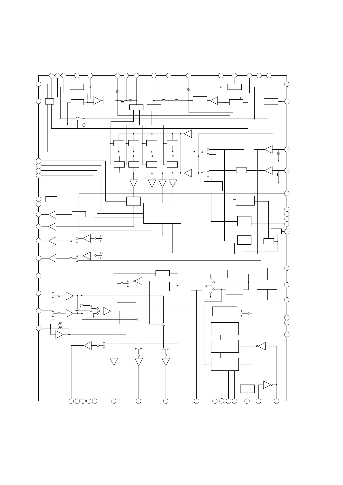
• IC Block Diagrams
1
2
3
4
5
6
7
8
9
10
11
12
13
14
15
30
29
28
27
26
25
24
23
22
21
20
19
18
17
16
CONTROL
LATCH
SHIFT RESISTOR
LEVEL SHIFT
CL
DI
CE
VEE
OUT
IN
OUT
IN
OUT
IN
VSS
S
RESET
VDD
OUT
ININ
OUT
IN
OUT
IN
– STANDBY Board –
IC950 NJM2103D
8
RESET
+
–
VSA
7
6
VSB/SESIN
V+
5
+
–
VSC
OUTC
GND
CR
1
2
+
–
3
4
VREF
Q
R S
+
–
– MAIN Board –
IC100 M62447SP
DVDD
42
1
OUT4
2
OUT3
OUT2
OUT1
AVDD
SW IN
GND S
SR IN
SL IN
GND C
C IN
GND R1
GND R2
GND L1
GND L2
R IN
GND LR
L IN
NC
3
4
5
6
7
8
9
10
11
12
13
14
15
16
17
18
21 – 19
OUTPUT
PORT
MICRO
COMPUTER
INTERFACE
41
40
39
38
37
36
35
34
33
32
31
30
29
22 – 28
CLK
DATA
LATCH
DGND
AGND
SW OUT
SR OUT
SL OUT
C OUT
R OUT
L OUT
AVSS1
AVSS2
NC
IC500 LC78212
7
IC300 LV1035M
R BPF2
R BPF1
S DC OUT
C DC OUT
R DC OUT
L DC OUT
V REF
VCC
C OUT
S OUT
R OUT
L OUT
GND
L IN
R IN
S IN
R BPF3
64 63 62 61 60 59 58 57 56 55 54 53 52 51 50 49
1
2
BPF
3
4
5
6
V REF
7
8
9
C
S
10
R
11
L
12
13
14
15
16
A
B
A
B
RECT
RECT
STRIM
L
R
S
L+R RECT
A
B
A
B
A
R
B
A
L
B
A
A
B
B
S
DC CUT2
L-R RECT
DC CUT1
VCS TH
LOGIC
FF
VCA VCA
VCA VCA VCA VCA
S
A
B
S
VCS 2
VCS 1
LOGIC LOGIC
S
MODE
A
B
A
VLR 2
VCA VCA
C MODE
STRIM
VOL/
MUTE
A
BB
L RECT
IN
FILTER
SRAM
PCM
PCM
RECT
RECT
B NR
OUT
FILTER
DC CUT4
VOL
CONTROL
FILTER
VLR 1
LR
VLR TH
LOGIC
DC
CUT
FF
A
B
A
B
CH
CONTROL
A
S
C
B
CONTROL
BPF
NOISE
NOISE
GEN
A
B
VOL
R RECT
DC CUT3
BPF
R
DEV
DATA
DECODER
L BPF3
L
OSC
48
47
46
45
44
43
42
41
40
39
38
37
36
35
34
33
L BPF2
L BPF1
RT IN
LT IN
DC CUT
C MODE
GND
NS BPF1
NS BPF2
OSC
CLK
DATA
ENABLE
DATA
CLK
VSS
VDD
1817
19 20 21 22 23 24 25 262728 29 30 31 32
NS
A/D
VCC
DELAY OUT
DET
IREF
GND
S-OUT
R-OUT
L-OUT
DC CUT
DC CUT
D/A
VDD
OSC
OSC
8
 Loading...