Sony TAEX-100 Service manual
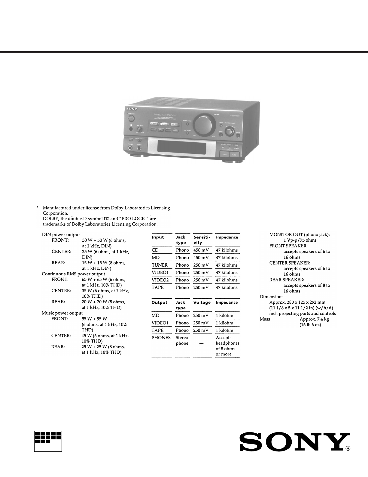
TA-EX100
SERVICE MANUAL
TA-EX100 is the amplifier
section in MHC-EX100AV.
SPECIFICATIONS
AEP Model
E Model
MICROFILM
General
Power requirements
AEP,German,Italian models:
220-230V AC, 50/60Hz
Other models:
110-120V or 220V-240V AC
adjustable, 50/60Hz
Power consumption
220W (active speakers not
included)
Design and specificatuons aer subject to change
without notice.
– Continued on next page –
AV AMPLIFIER
— 1 —

[ TEST MODE ]
Press SYSTEM POWER button, turn the power on and press DIS
PLAY and AUDIO buttons for two seconds at the same time to
enter in the test mode.
See the list below for check of mode and display.
Button
Display(mode)
PRO-LOGIC ON/OFF & MODE setting.
The display will change every pressing the
M.MENU
button.
PHANTOM(ON)n NORMALn WIDEn
3CH LOGICnTHROUGH(OFF)
P.FILE
PRO LOGIC
M.SOURCE
PRESENSE
MEMORY
NAME
KARAOKE
PON/MPX
7kHz LPF ON/OFF
B DECODER ON/OFF
LEFT (Lch test tone output)
RIGHT (Rch test tone output)
CENTER (Cch test tone output)
REAR (Sch test tone output)
FL & LED all light up
Note:
Turn off the test tone with pressing the M.MENU button to change
the mode.
Press the corresponded button to each channel to fix each
channel of the test tone after the M.SOURCE button.
TABLE OF CONTENTS
SECTION 1. GENERAL................................................. 3
SECTION 2. DISASSEMBLY
2-1. Front Panel Assembly........................................................... 4
2-2. Audio Board and DSP Board ............................................... 4
2-3. Main Board........................................................................... 5
2-4. Back Panel Assembly ........................................................... 5
SECTION 3. DIAGRAMS
3-1. Circuit Boards Location ....................................................... 6
3-2. IC Pin Function
• IC601 System Control (HD6433927B97F) ....................... 7
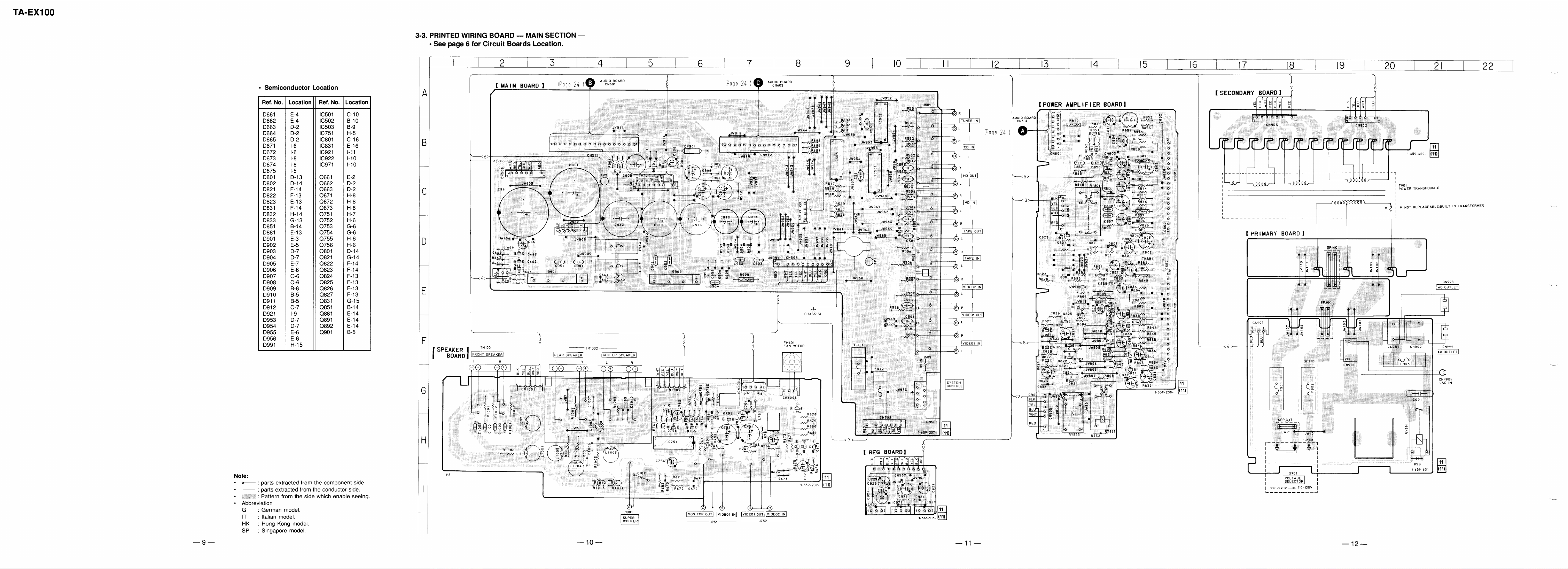
3-3. Printed Wiring Board — Main Section — ........................... 9
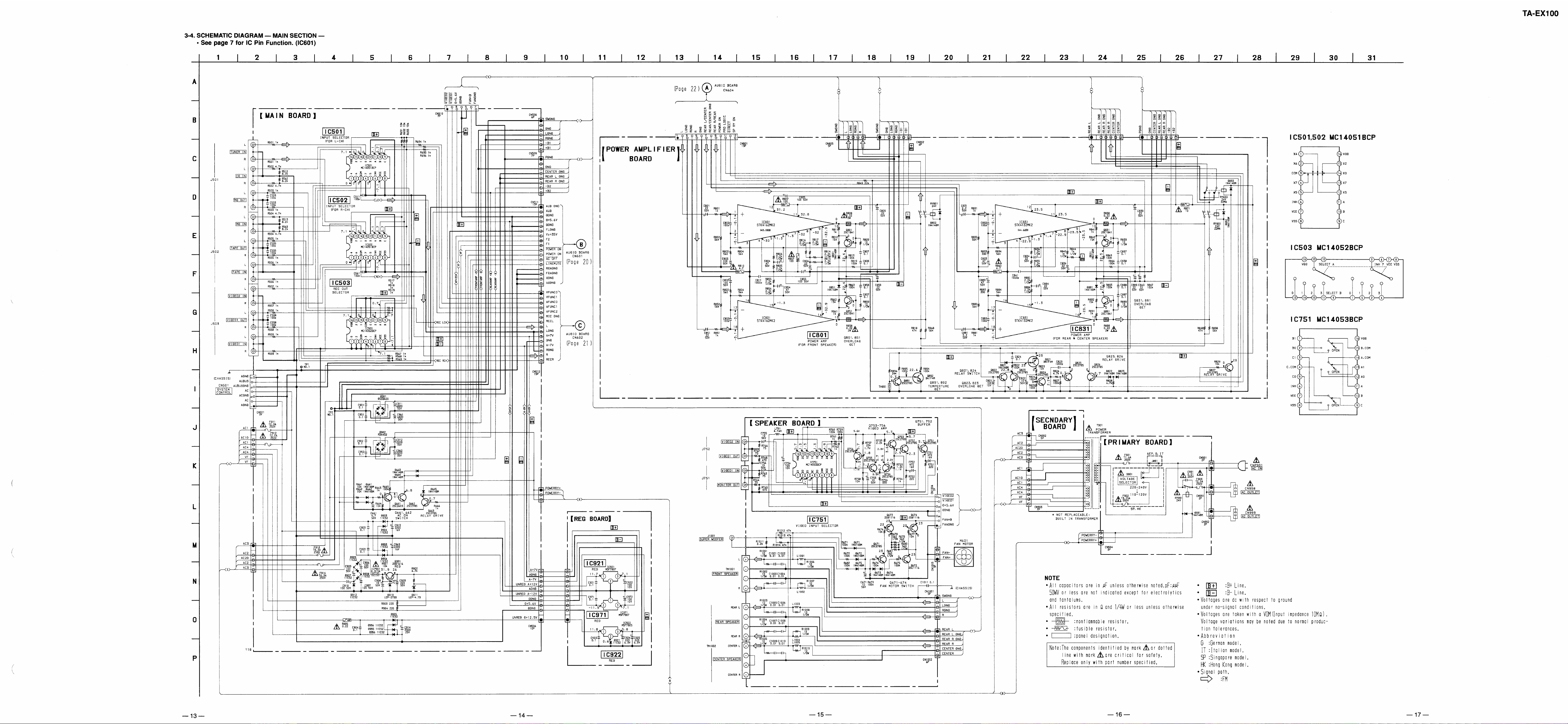
3-4. Schematic Diagram — Main Section — ............................13
3-5. Schematic Diagram — Audio/Panel Section —................. 18
3-6. Printed Wiring Board — Audio/Panel Section — ..............23
3-7. Printed Wiring Board — DSP Section — .......................... 26
3-8. Schematic Diagram — DSP Section — .............................29
3-9. IC Block Diagrams — DSP Section —.............................. 33
SECTION 4. EXPLODED VIEWS
4-1. Front Panel Section 1 .........................................................35
4-2. Front Panel Section 2 .........................................................36
4-3. Chassis Section...................................................................37
SECTION 5. ELECTRICAL PARTS LIST................. 38
Press the SYSTEM POWER button to cancel the test mode.
SAFETY-RELATED COMPONENT WARNING !!
COMPONENTS IDENTIFIED BY MARK ! OR DOTTED
LINE WITH MARK ! ON THE SCHEMATIC DIAGRAMS
AND IN THE PARTS LIST ARE CRITICAL TO SAFE
OPERATION. REPLACE THESE COMPONENTS WITH
SONY PARTS WHOSE PART NUMBERS APPEAR AS
SHOWN IN THIS MANUAL OR IN SUPPLEMENTS
PUBLISHED BY SONY .
MODEL IDENTIFICATION
– BACK PANEL –
PARTS No.
MODEL
AEP model
German model
Italian model
Singapore model
Hong Kong model
PARTS No.
4-978-785-0π
4-978-785-1π
4-978-785-2π
— 2 —
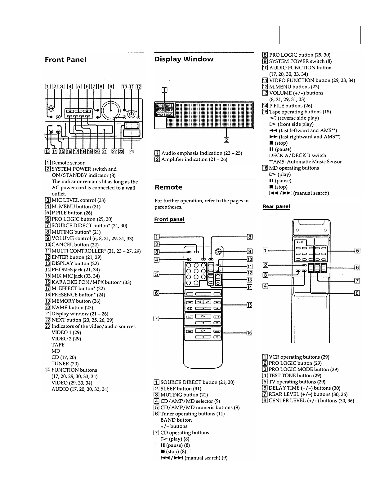
SECTION 1
GENERAL
This section is extracted from
instruction manual.
— 3 —
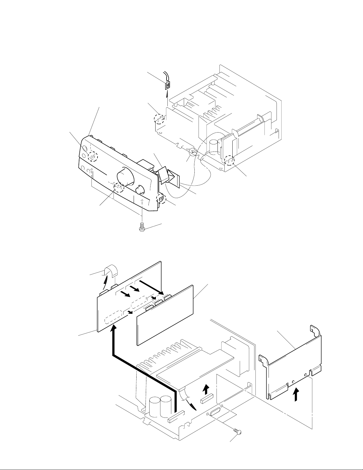
SECTION 2
DISASSEMBLY
Note: Follow the disassembly procedure in the numerical order given.
2-1. FRONT PANEL ASSEMBLY
3
Ground clip
5
Remove the front panel assembly
with care to claws.
Claw
1
Connector
(CN603, Flat type
Claw
15 core)
Claw
Claw
Claw
2-2. AUDIO BOARD AND DSP BOARD
1
Connector
(CN604, Flat type 13 core)
4
Audio board
Claw
4
Three screws
(BVTP 3x8)
2
Connector
(CN601, Flat type 29 core)
5
DSP board
3
PC board retainer
— 4 —
2
Two screws
(BVTT 3x6)
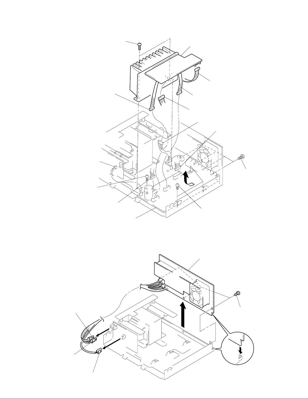
2-3. MAIN BOARD
0
!¡
Screw
(BVTP 3x8)
5
4
Connector (CN508)
Connector
(CN993)
Two screws
(BVTP 3x8)
6
AMP board
1
2
Connector (CN509)
3
Connector (CN803)
8
Connector (CN903)
Connector (CN805)
7
Connector (CN506)
!£
Four screws
(BVTP 3x8)
9
2-4. BACK PANEL ASSEMBLY
3
Connector
(CN992)
Connector
(CN503)
!¢
Remove the main board
direction of arrow.
!™
Three screws
(BVTP 3x8)
5
Back panel assembly
4
Three screws
(BVTP 3x8)
2
Connector
(CN991)
1
Connector
(CN901)
Note for installation
— 5 —
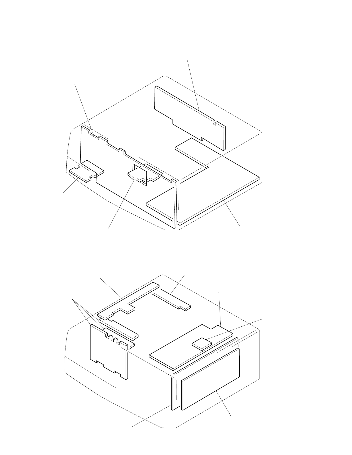
3-1. CIRCUIT BOARDS LOCATION
PANEL board
SECTION 3
DIAGRAMS
SPEAKER board
HP/MIC board
PRIMARY board
VOL board
COVER board
MAIN board
SECONDARY board
POWER AMPLIFIER board
REG board
AUDIO board
DSP board
— 6 —
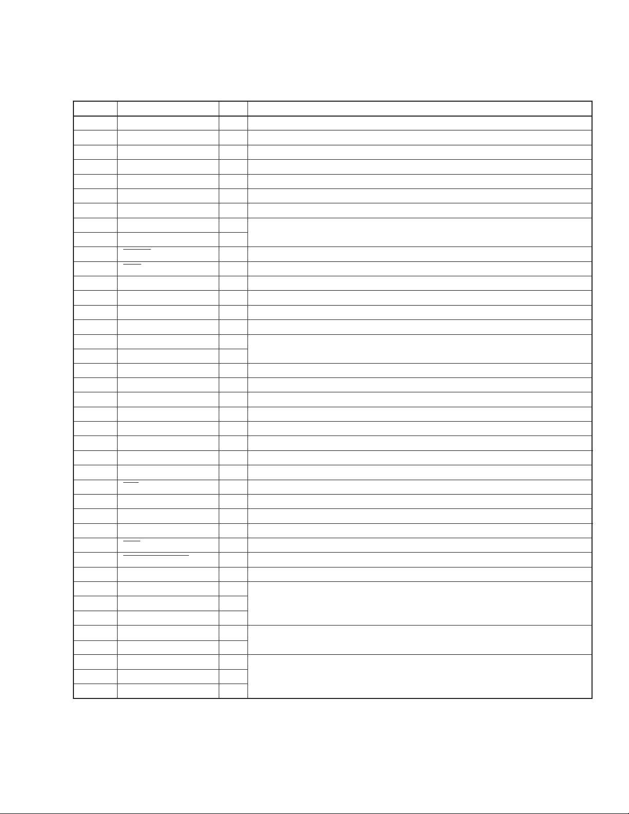
3-2. IC PIN FUNCTION
• IC601 SYSTEM CONTROL (HD6433927B97F)
Pin No.
1
2 to 4
5
6
7
8
9
10
11
12
13
14
15
16
17
18
19
20
21
22
23
24
25
26
27 to 31
32
33
34
35 to 38
39
40
41 to 46
47
48
49
50
51
52
53
54
Pin Name I/O
VOLUME IN
KEY 0 to KEY 2
AVss
TEST
X2
X1
Vss
OSC 1
OSC 2
RESET
NMI
POWER
SP RELAY
PROLOGIC RELAY
DIRECT
VOL-UP
VOL-DOWN
LINE MUTE
–20 dB MUTE
—
—
SIRCS
AUB IN
AUB OUT
—
STB
CLK
DATA
—
MIC IN
KARAOKE PON
—
A FUNC 0
A FUNC 1
A FUNC 2
V FUNC 0
V FUNC 1
2DB
4DB
8DB
Not used. (Ground)
—
Key matrix input.
I
Ground
—
Ground
—
Not used. (open)
—
+5V power supply.
—
Ground
—
I
Clock (10 MHz).
O
System reset input.
I
AC OFF detect.
I
Power relay output.
O
Speaker relay output. (power ON/OFF)
O
Speaker relay output. (PROLOGIC ON/OFF)
O
Speaker relay. (DIRECT)
O
O
MIC VOL up/down output.
O
LINE mute output. (power OFF “High”)
O
–20 dB mute output.
O
Not used. (open)
—
Not used. (Ground)
—
SIRCS signal input
I
Audio bus input.
I
Audio bus output.
O
Not used. (Ground)
—
LED strobe output.
O
LED clock output.
O
LED serial data output.
O
Not used. (Ground)
—
Microphone detect control. (mic on “Low”)
O
Not used. (Ground)
—
Not used. (Ground)
—
O
Audio function control output.
O
O
O
Video function control output.
O
O
ATT control.
O
O
Function
— 7 —
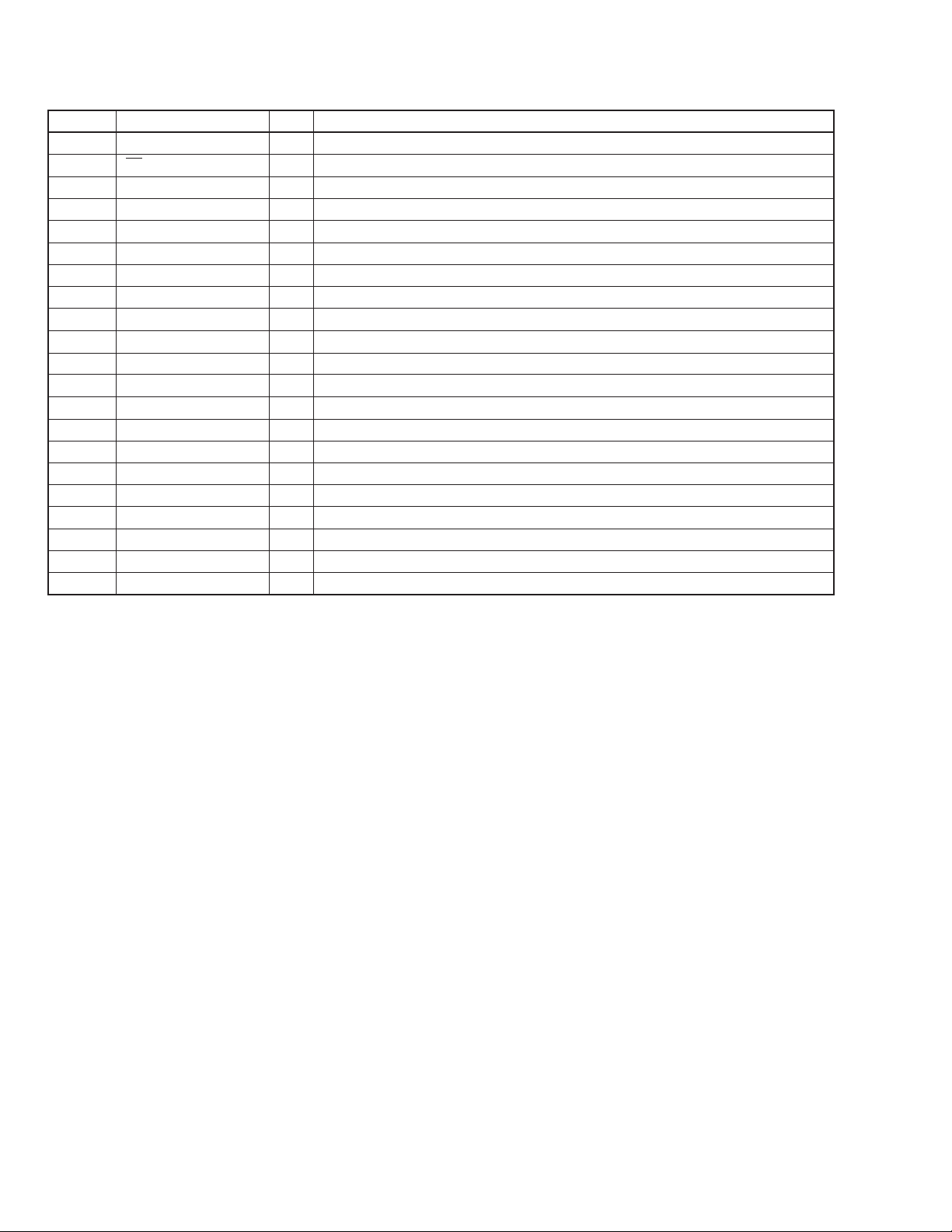
Pin Name
55
56
57
58
59
60
61
62
63
64
65
66
67
68
69
70
71
72
73 to 78
79
80
• Abbreviation
FL : Fluorescent Indicator Tube
—
CL
DA TA
LATCH
CLK
DATA OUT
DATA IN
CLK
Vcc
LATCH
NSQCT
READY
INIT
ATT
CLK
DR LATCH
DF LATCH
AVcc
—
JOG 1
JOG 2
I/O FunctionPin No.
Not used. (Ground)
—
FL clear output. IC701, 702 control.
O
FL data output. IC701, 702 control.
O
FL latch output. IC701, 702 control.
O
FL clock output. IC701, 702 control.
O
DSP data output. IC202 control.
O
DSP data input. IC202 control.
I
DSP clock output. IC202 control.
O
+5V power supply.
—
DSP latch output.
O
DSP test data output.
O
READY signal input from DSP.
I
DA/AD/DSP IC initial output.
O
DA ATT output.
O
DA clock output.
O
DA rear/center latch output.
O
DA front latch output.
O
+5V power supply.
—
Not used. (Ground)
—
JOG A input.
I
JOG B input.
I
— 8 —
 Loading...