

Sony stv9553 Service Manual
STV9553
10.5 ns TRIPLE-CHANNEL HIGH VOLTAGE VIDEO AMPLIFIER
FEATURES
■ Triple-channel video amplifier
■ Supply voltage up to 115 V
■ 80V Output dynamic range
■ Perfect for PICTURE BOOST application
requiring high video amplitude
■ Pinning for easy PCB layout
■ Supports DC coupling (optimum cost saving)
and AC coupling applications.
■ Built-in Voltage Gain: 20 (Typ.)
■ Bandwidth: 33 MHz (Typ.)
■ Very low stand-by power consumption
■ Perfectly matched with the STV921x
preamplifiers
DESCRIPTION
The STV9553 is a triple-channel video amplifier
designed in a 120V-hi gh voltage technology and
able to drive in DC-coupl in g mo de the 3 cathodes
of a CRT monitor.
The STV9553 supports PICTURE BOOST
applications where video ampl itude up to 50V or
PIN CONNECTIONS
above is required, ensu ring a maximum quality of
the still pictures or moving video.
Perfecly matched with the STV921x ST
preamplifiers, it provides a highly perfo rmant and
very cost effective video system.
CLIPWATT 11
(Plastic Package)
ORDER CODE: STV9553
11
10
9
8
7
6
5
4
3
2
1
OUT1
OUT2
OUT3
GNDP
V
DD
GNDS
GNDA
IN3
V
CC
IN2
IN1
Version 4.1
September 2003 1/24
1

Table of Contents
1 BLOCK DIAGRAM . . . . . . . . . . . . . . . . . . . . . . . . . . . . . . . . . . . . . . . . . . . . . . . . . . . . . . . . . . . 3
2 PIN DESCRIPTION . . . . . . . . . . . . . . . . . . . . . . . . . . . . . . . . . . . . . . . . . . . . . . . . . . . . . . . . . . 3
3 ABSOLUTE MAXIMUM RATINGS . . . . . . . . . . . . . . . . . . . . . . . . . . . . . . . . . . . . . . . . . . . . . . 4
4 THERMAL DATA . . . . . . . . . . . . . . . . . . . . . . . . . . . . . . . . . . . . . . . . . . . . . . . . . . . . . . . . . . . . 4
5 ELECTRICAL CHARACTERISTICS . . . . . . . . . . . . . . . . . . . . . . . . . . . . . . . . . . . . . . . . . . . . . 5
6 THEORY OF OPERATION . . . . . . . . . . . . . . . . . . . . . . . . . . . . . . . . . . . . . . . . . . . . . . . . . . . . 7
6.1 General . . . . . . . . . . . . . . . . . . . . . . . . . . . . . . . . . . . . . . . . . . . . . . . . . . . . . . . . . . . . . 7
6.2 Output voltage . . . . . . . . . . . . . . . . . . . . . . . . . . . . . . . . . . . . . . . . . . . . . . . . . . . . . . . . 8
7 POWER DISSIPATION . . . . . . . . . . . . . . . . . . . . . . . . . . . . . . . . . . . . . . . . . . . . . . . . . . . . . . . 9
8 TYPICAL PERFORMANCE CHARACTERISTICS . . . . . . . . . . . . . . . . . . . . . . . . . . . . . . . . . 10
9 INTERNAL SCHEMATICS . . . . . . . . . . . . . . . . . . . . . . . . . . . . . . . . . . . . . . . . . . . . . . . . . . . . 11
10 APPLICATION HINTS . . . . . . . . . . . . . . . . . . . . . . . . . . . . . . . . . . . . . . . . . . . . . . . . . . . . . . . 12
10.1 How to choose the high supply voltage value (VDD) in DC coupling mode . . . . . . . . 12
10.2 Arcing Protection: schematics . . . . . . . . . . . . . . . . . . . . . . . . . . . . . . . . . . . . . . . . . . . 12
10.3 Arcing protection: layout and decoupling . . . . . . . . . . . . . . . . . . . . . . . . . . . . . . . . . . . 13
10.4 Video response optimization: schematics in DC-coupling mode . . . . . . . . . . . . . . . . . 14
10.5 Video response optimization: outputs networks . . . . . . . . . . . . . . . . . . . . . . . . . . . . . . 15
10.6 Video response optimization: inputs networks . . . . . . . . . . . . . . . . . . . . . . . . . . . . . . . 15
10.7 Video response optimization: layout and decoupling . . . . . . . . . . . . . . . . . . . . . . . . . . 15
10.8 AC - Coupling mode . . . . . . . . . . . . . . . . . . . . . . . . . . . . . . . . . . . . . . . . . . . . . . . . . . . 16
10.9 Stand-by mode, spot suppression . . . . . . . . . . . . . . . . . . . . . . . . . . . . . . . . . . . . . . . . 17
10.10 Conclusion . . . . . . . . . . . . . . . . . . . . . . . . . . . . . . . . . . . . . . . . . . . . . . . . . . . . . . . . . . 18
11 PACKAGE MECHANICAL DATA . . . . . . . . . . . . . . . . . . . . . . . . . . . . . . . . . . . . . . . . . . . . . . 22
2/24
2
2
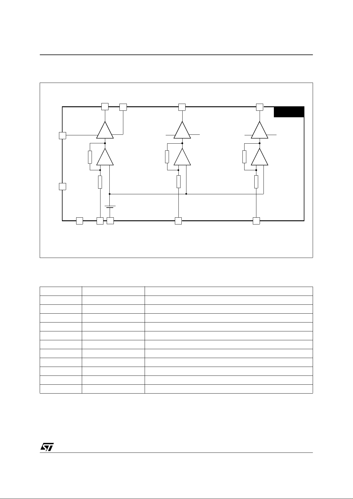
1 BLOCK DIAGRAM
STV9553
7
VDD
3
VCC
OUT1
11
GNDP
8
OUT2
10
OUT3
9
STV9553
V
DD
V
REF
6
1
5
GNDP
2
VDD
GNDP
4
IN3IN2IN1 GNDAGNDS
2 PIN DESCRIPTION
Pin Name Function
1 IN1 Video Input (channel 1)
2 IN2 Video Input (channel 2)
3 VCC Low Supply Voltage
4 IN3 Video Input (channel 3)
5 GNDA Ground Analog
6 GNDS Ground Substrat
7 VDD High Supply Voltage
8 GNDP Ground Power
9 OUT3 Video output (channel 3)
10 OUT2 Video output (channel 2)
11 OUT1 VIdeo output (channel 1)
3/24
3
STV9553
3 ABSOLUTE MAXIMUM RATINGS
Symbol Parameter Value Unit
V
V
V
I
I
V
IN Max
V
IN Min
T
DD
CC
ESD
OD
OG
T
J
STG
High supply voltage 120 V
Low supply voltage 16.5 V
ESD susceptibility
Human Body Model (100pF discharged through 1.5KΩ)
EIAJ norm (200pF discharged through 0Ω)
Output source current (pulsed < 50µs) 80 mA
Output sink current (pulsed < 50µs) 80 mA
Maximum Input Voltage VCC + 0.3 V
Minimum Input Voltage - 0.5 V
Junction Temperature 150 °C
Storage Temperature -20 + 150 °C
2
300
kV
V
4 THERMAL DATA
Symbol Parameter Value Unit
R
th (j-c)
R
th (j-a)
Junction-Case Thermal Resistance (Max.) 3 °C/W
Junction-Ambient Thermal Resistance (Typ.) 35 °C/W
4/24
3
5 ELECTRICAL CHARACTERISTICS
Symbol Parameter Test Conditions Min. Typ Max Unit
SUPPLY parameters (VCC = 12V, VDD = 110V, Tamb = 25 °C, unless otherwise specified)
V
DD
V
CC
I
DD
I
DDS
I
CC
STATIC parameters (VCC = 12V, VDD = 110V, Tamb = 25 °C)
V
OUT
dV
/dV
OUT
dV
OUT
d∆V
OUT
R
IN
V
SATH
V
SATL
G Video Gain V
LE Linearity Error 17 V<V
V
REF
High supply voltage 20 110 115 V
Low supply voltage 10 12 15 V
VDD supply current V
VDD stand-by supply current
VCC supply current V
= 50V 15 m A
OUT
: switched off (<1.5V)
V
CC
V
: low (Note 1)
OUT
= 50V 40 m A
OUT
60 µA
DC output voltage VIN=1.90 V 77 80 83 V
High voltage supply rejection V
DD
/dT Output voltage drift versus temperature V
Output voltage matching versus
/dT
temperature (No te 2)
Video input resistor V
Output saturation voltage to supply I0 = -60mA (Note 3)
= 50V 0.5 %
OUT
= 80V 15 mV/°C
OUT
V
= 80V 1 mV/°C
OUT
= 50V 2 kΩ
OUT
V
- 6.5
DD
Output saturation voltage to GND I0 = 60mA (Note 3)11V
= 50V 20
OUT
OUT<VDD
-15 V 3 8 %
Internal voltage refere nc e 5.6 V
STV9553
V
Note 1: The STV9553 goes into stand-by mode when Vcc is switched off (<1.5V).
In stand-by mode, Vout is set to low level.
Note 2: Matching measured between each channel.
Note 3: Pulsed current width < 50µs
5/24
3
STV9553
ELECTRICAL CHARACTERISTICS (continued)
Symbol Parameter Test Conditions Min. Typ Max Unit
DYNAMIC parameters (see Figure 1)
t
Rise time VDC=50V, ∆V=40V
R
OS
OS
t
F
R
F
Fall time VDC=50V, ∆V=40V
Overshoot, white to black transition 5 %
Overshoot, black to white transition 0 %
∆G Low frequency gain matching (Note 4)V
BW Bandwidth at -3d B V
t
SET
2.5% Settling time VDC=50V, ∆V=40V
V
CT
CT
L
H
Low frequency crosstalk
High frequency crosstalk
f = 1 MHz 50 dB
V
f = 20MHz 32 dB
= 50V, f=1MHz 5 %
DC
=50V, ∆V=20V
DC
=50V, ∆V=20V
DC
=50V, ∆V=20V
DC
PP
PP
PP
PP
PP
PP
DYNAMIC parameter in PICTURE BOOST condition (Note 5)
t
OS
PB
PB
Rise/fall time VDC=50V, ∆V=60V
Overshoot white to black or black to white
transition
V
=50V, ∆V=60V
DC
PP
PP
Note 4: Matching measured between each channel.
Note 5: PICTURE BOOST condition (video amplitude at 50V or above) is used in some applications when displaying
still picture or moving video. In this condition the high level of contrast improves the pictures quality at the
expense of the video performances (t
, tF and Overshoot) which are slightly deteriorated.
R
9.8 ns
11.8 ns
33 MHz
15 ns
15 ns
9%
Figure 1. AC test circuit
50
Ω
IN
6/24
3
V
1
STV9553
CC
110V12V
V
3
V
REF
DD
7
= 300
R
OUT
11
8
P
CL=8pF
∆
DC
V
V
Ω
GNDP
5
GNDA
6 THEORY OF OPERATION
6.1 General
STV9553
The STV9553 is a three-chann el video amplifier supp lied by a low supply voltag e: V
high supply voltage: V
The high values of V
(up to 115V).
DD
supplying the amplifier output stage allow direct control of the CRT cathodes (DC
DD
(typ.12V) and a
CC
coupling mode).
In DC coupling mod e, the app licatio n schemati c is ver y simple and only a few e xternal comp onents ar e
needed to drive the c athodes. In particu lar, there is no ne ed of the D C-restore circuitry wh ich is us ed in
classical AC coupling applications.
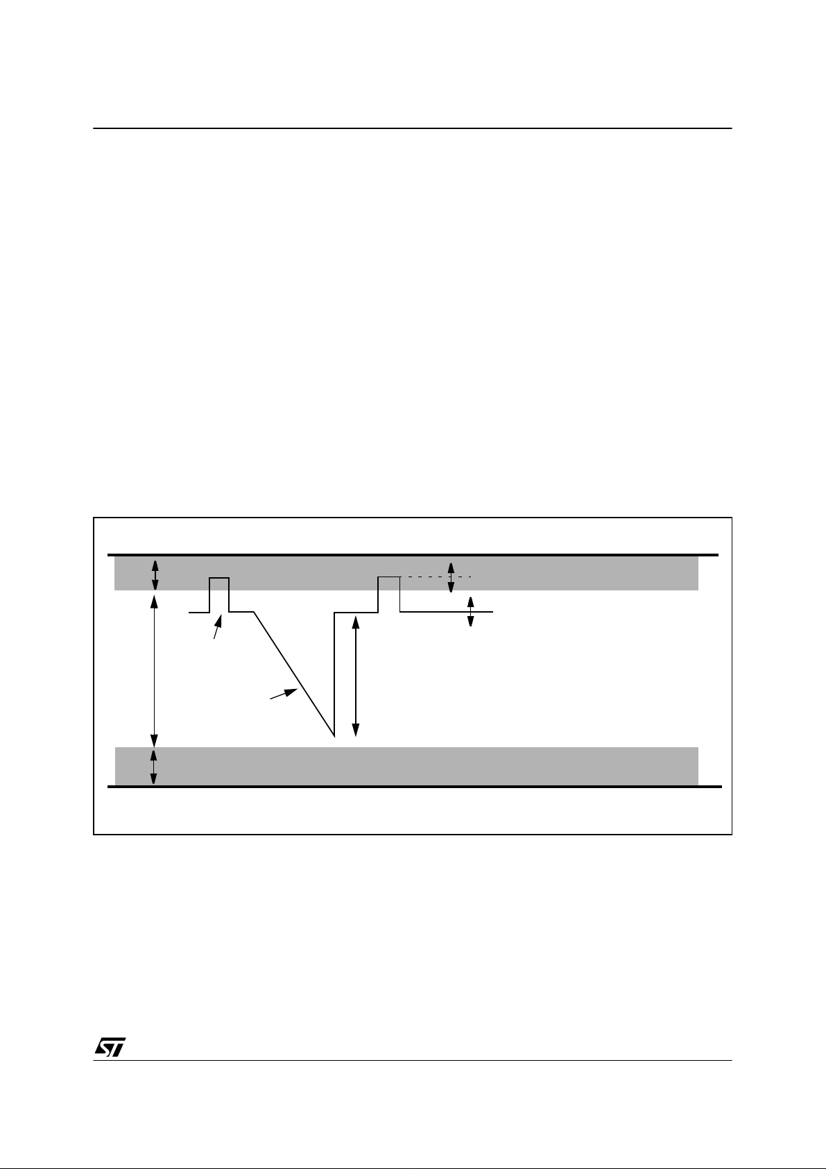
The output voltage range is wide enough (Figure 2) to provide simultaneously :
– Cut-off adjustment (typ. 25V)
– Video contrast (typ. up to 40V),
– Brightness (with the remaining voltage range).
In normal operation, the output video signal mus t remain inside the linear region whatever the cut-off,
brightness and contrast adjustments are.
Figure 2. Output signal, level adjustments
V
DD
15V
(A) Top Non-Linear Region
(B) Cut-off Adjust. (25V Typ.)
(C) Brightness Adjust. (10V Typ.)
17V
Blanking pulse
Linear region
(E)
GND
(D) Contrast Adjust. (40V Typ.)
Video Signal
Bottom Non-Linear Region
7/24
3
STV9553
6.2 Output voltage
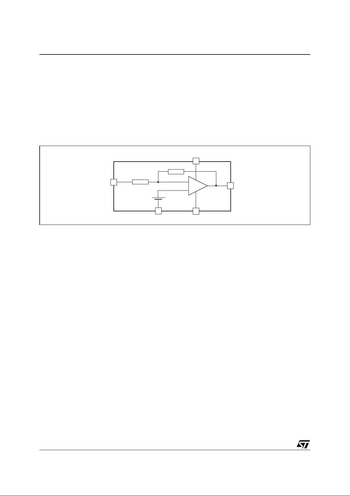
A very simplified schematic of each STV9553 channel is shown in Figure 3.
The feedback network of each channel is integrated with a typical built-in voltage gain of G=20 (40k/2k).
The output voltage V
V
=(G+1) x V
OUT
for G = 20 and V
V
=117.6-20xV
OUT
REF
REF
is given by the following formula:
OUT
- (G xVIN)
= 5.6V, we have
IN
Figure 3. Simplified schematic of one channel
2k
IN
V
REF
GNDA
40k
V
DD
-
+
GNDP
OUT
8/24
 Loading...