

Page 1
ST-S5
SERVICE MANUAL
Ver 1.0 2001.04
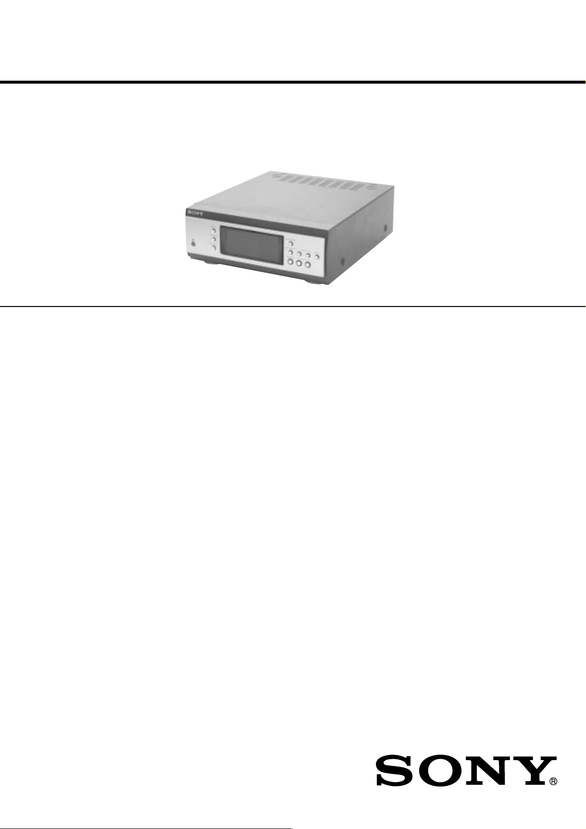
ST-S5 is the tuner section
in MHC-S7AV.
SPECIFICATIONS
Tuner section
FM stereo, FM/AM superheterodyne tuner
FM tuner section
Tuning range 87.5 – 108.0 MHz
Antenna FM lead antenna
Antenna terminals 75 ohm unbalanced
Intermediate frequency 10.7 MHz
AEP Model
UK Model
E Model
Australian Model
AM tuner section
Tuning range
AEP, UK models:
Other models: 531 – 1,602 kHz
Antenna AM loop antenna
Antenna terminals External antenna terminal
Intermediate frequency 450 kHz
Dimensions (w/h/d)
Mass
Design and specifications are subject to change
without notice.
531 – 1,602 kHz
(with the interval set at
9 kHz)
(with the interval set at
9 kHz)
530 – 1,710 kHz
(with the interval set at
10 kHz)
Approx. 280 x 108 x 340 mm
Approx. 2.1 kg
FM STEREO/FM-AM
9-873-832-11 Sony Corporation
2001D0500-1 Home Audio Company
C 2001.4 Shinagawa Tec Service Manual Production Group
SUPERHETERODYNE TUNER
Page 2

ST-S5
TABLE OF CONTENTS
1. SERVICING NOTES ................................................ 3
2. GENERAL
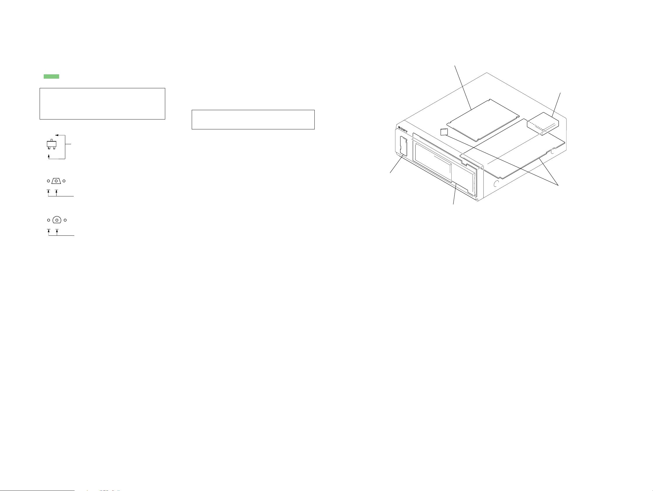
Location of Controls ....................................................... 4
Setting the Time .............................................................. 5
3. DISASSEMBLY
3-1. Disassembly Flow ........................................................... 6
3-2. Cover ............................................................................... 7
3-3. Front Panel Section ......................................................... 7
3-4. PANEL Board, SIRCS Board ......................................... 8
3-5. Tuner pack (FM/AM)...................................................... 8
3-6. MAIN Board ................................................................... 9
3-7. DSP Board....................................................................... 9
4. TEST MODE.............................................................. 10
5. DIAGRAMS
5-1. Note for Printed Wiring Boards and
Schematic Diagrams ....................................................... 11
5-2. Schematic Diagram – MAIN Board (1/2) – .................. 12
5-3. Schematic Diagram – MAIN Board (2/2) – .................. 13
5-4. Printed Wiring Board – MAIN Board – ........................ 14
5-5. Printed Wiring Board – DSP Board –............................ 15
5-6. Schematic Diagram – DSP Board (1/2) – ..................... 16
5-7. Schematic Diagram – DSP Board (2/2) – ..................... 17
5-8. Printed Wiring Boards – PANEL Section – .................. 18
5-9. Schematic Diagram – PANEL Section – ....................... 19
5-10. IC Pin Function Description ........................................... 21
Notes on chip component replacement
• Never reuse a disconnected chip component.
• Notice that the minus side of a tantalum capacitor may be dam-
aged by heat.
SAFETY-RELATED COMPONENT WARNING!!
COMPONENTS IDENTIFIED BY MARK 0 OR DOTTED
LINE WITH MARK 0 ON THE SCHEMATIC DIA GRAMS
AND IN THE PARTS LIST ARE CRITICAL TO SAFE
OPERATION. REPLACE THESE COMPONENTS WITH
SONY PARTS WHOSE PART NUMBERS APPEAR AS
SHOWN IN THIS MANUAL OR IN SUPPLEMENTS PUBLISHED BY SONY.
6. EXPLODED VIEWS
6-1. Cover, Front Panel Section ............................................. 28
6-2. Chassis Section ............................................................... 29
7. ELECTRICAL PARTS LIST ............................... 30
2
Page 3
SECTION 1
PART No.
SERVICING NOTES
ST-S5
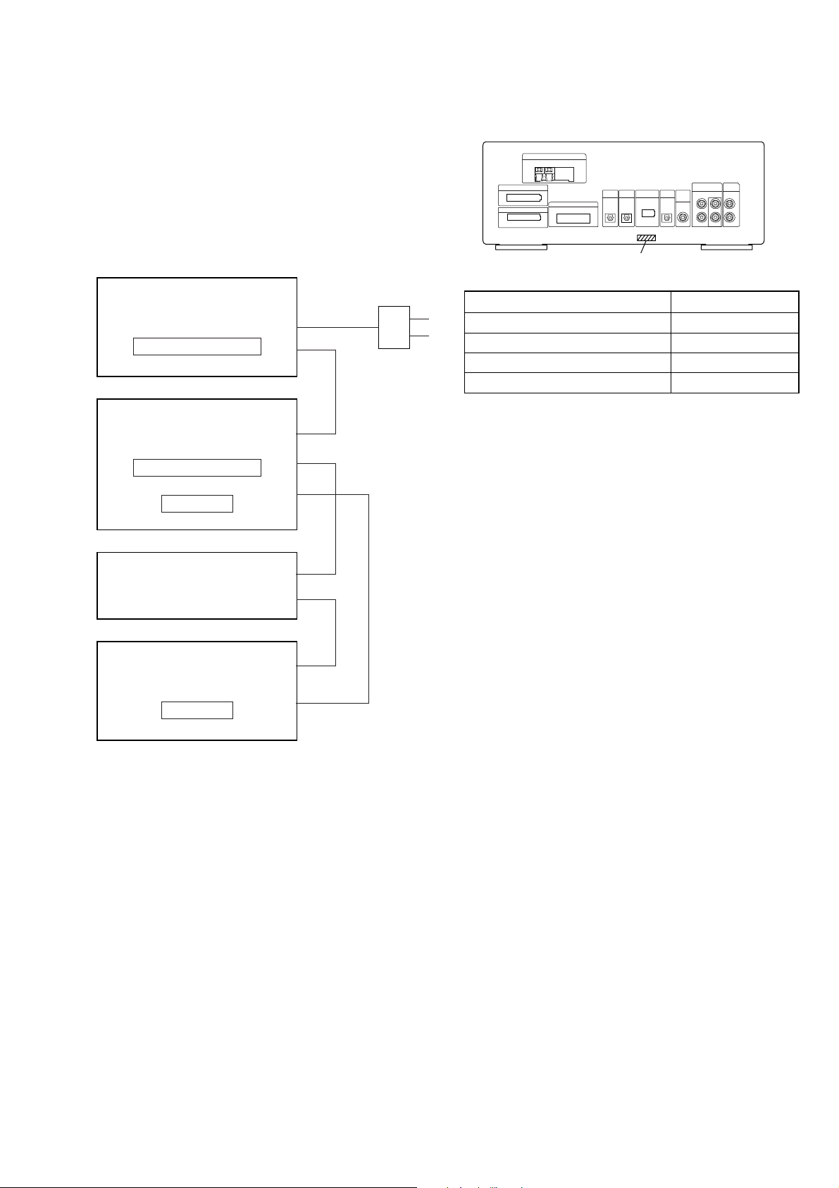
This set is a component of the MHC-S7AV.
The MHC-S7AV system configuration is as shown below, and
therefore it does not operate normally unless all four components
are connected.
In performing the repair, connect all components with the system
cables.
Note: The precaution to the users is described on the label stuck
on the back panel (CD player) and in the troubleshooting section
in the Operation Manual.
System Configuration:
AC IN
TA
POWER SUPPLY
ST
SYSTEM & CD µcon
DISPLAY
• MODEL IDENTIFICATION
– Rear Panel –
MODEL PART No.
AEP and UK models 4-232-327-0
Australian model 4-232-327-1[]
Mexican model 4-232-327-4
Korean model 4-232-327-9
[]
[]
[]
CDP
TC
TC µcon
3
Page 4
ST-S5
LOCATION OF CONTROLS
– Front Panel –
SECTION 2
GENERAL
This section is extracted from
instruction manual.
– Rear Panel –
2
3
qh qj
1
4 5 6 7
8
qk
ql
–
–
09qa
w;
+
+
wawswdwfwgwh
CLOCK/TIMER wg (13, 21, 29)
DISPLAY qh (13, 16, 18, 29, 35)
ENTER w; (17, 18)
IR receptor wh
PRESET +/– ws (17, 18)
PTY (AEP, UK models only)
STEREO/MONO qj (17)
TIMER SELECT wf (22, 30)
TUNER/BAND wd (17)
TUNER MEMORY qk (17)
TUNING +/– ql
1 ANTENNA terminal
2 SYSTEM CONTROL 1 connector (TO TA-S7AV)
3 SYSTEM CONTROL 2 connector (TO TA-S7AV)
4 SYSTEM CONTROL 3 connector (FROM CDP-S3)
5 OPTICAL IN terminal
6 OPTICAL IN terminal (FROM CDP-S3)
7 SYSTEM CONTROL 4 connector (TO TC-S3)
8 OPTICAL OUT terminal
9 SUB WOOFER OUT jack
0 MD IN/OUT jack
qa VIDEO (AUDIO) IN jack
(17)
wa
(18)
4
Page 5
Setting the time
1
Turn on the system.
2
Press CLOCK/TIMER (or CLOCK/TIMER
SET on the remote).
When you set the time for the first time,
proceed to step 5.
3
Press O or o repeatedly to select
“CLOCK SET”.
4
Press ENTER (A/V amplifier or remote).
5
Press O or o repeatedly to set the hour.
6
Press ENTER (A/V amplifier or remote).
7
Press O or o repeatedly to set the
minutes.
8
Press ENTER (A/V amplifier or remote).
Tip
If you have made a mistake or want to change the
time, start over from step 2.
Note
The clock settings are canceled when you disconnect
the power cord or if a power failure occurs.
Remote Control
123
ST-S5
es
ea
e;
wl
wk
wj
wh
wg
wf
wd
ws
wa
w;
ql
qk
CD H es (14, 15)
CHECK 5 (15)
CLEAR 6 (15)
CLOCK/TIMER SELECT qj
(30)
CLOCK/TIMER SET qk (13, 21,
29)
DBFB qg (23)
DISPLAY ws (13, 16, 18, 29, 35)
D.SKIP 4 (14)
ENTER wg (10, 12, 13, 15, 17,
18, 21, 22, 26–30)
EQ qd (27)
EQ ON/OFF qf (10, 28)
FUNCTION wf (10, 14, 15, 20,
21, 31)
GROOVE wa (23)
SET UP qs (10, 12, 26, 28, 29)
SLEEP 7 (29)
SUR wd (25)
TA P E A hH ea (19, 35)
TA P E B hH e; (19, 20, 35)
H
hH
hH
.
>
x
Mm
X
O
Pp
o
4
5
6
7
8
9
q;
qa
qs
qd
qf
qg
qh
qj
TUNER/BAND wl (17)
TUNING + 9 (17)
TUNING – wh (17)
TV CH +/– ql
TV VOL +/– w;
TV @/1 2
TV/VIDEO 1
VOL +/– qh
BUTTON DESCRIPTIONS
@/1 (power) 3
X (pause) q;
x (stop) 8
. (go back) wk
> (go forward) wj
m (rewind) wh
M (fast forward) 9
O/o/P/p
qa
5
Page 6
ST-S5
• This set can be disassembled in the order shown below.
3-1. DISASSEMBLY FLOW
SET
3-2. COVER
(Page 7)
SECTION 3
DISASSEMBLY
3-3. FRONT PANEL SECTION
(Page 7)
3-4. PANEL BOARD,
SIRCS BOARD
(Page 8)
3-5. TUNER PACK (FM/AM)
(Page 8)
3-6. MAIN BOARD
(Page 9)
3-7. DSP BOARD
(Page 9)
6
Page 7
Note: Follow the disassembly procedure in the numerical order given.
)
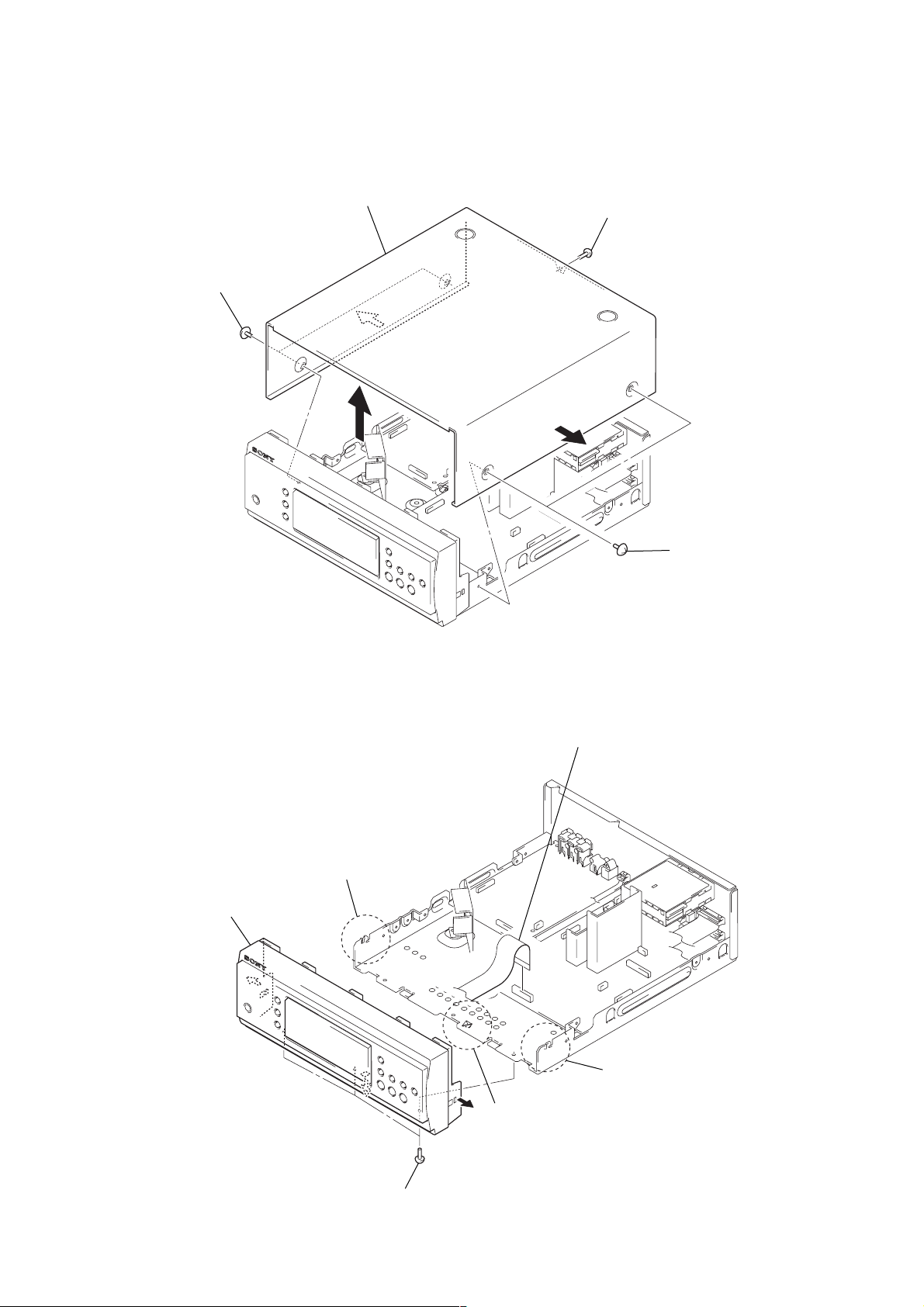
3-2. COVER
3
cover
2
two screws
(case 3 TP2)
1
screw
(+BVTT3
×
6 (S))
ST-S5
3-3. FRONT PANEL SECTION
3
two claws
4
front panel section
2
1
wire (flat type) (19 core)
(CN502)
two screws
(case 3 TP2
2
three screws
(BVTP3
3
two claws
3
claw
×
8)
7
Page 8
ST-S5
3-4. PANEL BOARD, SIRCS BOARD
6
SIRCS board
5
two claws
2
two screws
(BVTP2.6
×
8)
4
PANEL board
2
four screws
(BVTP2.6
1
wire (flat type) (19 core)
(CN602)
×
8)
2
screw
(BVTP2.6
(AEP, UK models)
×
8)
3-5. TUNER PACK (FM/AM)
1
wire (flat type) (11 core)
(Korean, Mexican and Australian models)
wire (flat type) (15 core)
(AEP, UK models)
(CN506)
3
two claws
3
tuner pack (FM/AM)
2
two screws
(BVTP3 × 8)
8
Page 9
r
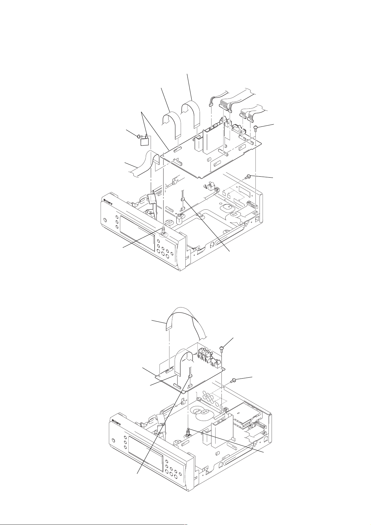
3-6. MAIN BOARD
4
1
wire (flat type) (19 core)
(CN502)
screw
(BVTP3
1
wire (flat type) (21 core)
(CN509)
6
MAIN board
×
8)
1
wire (flat type) (23 core)
(CN508)
2
five connectors
(CN510, 5031, 5032, 5041, 5042)
4
two screws
(BVTP3 × 8)
3
three screws
(BVTP3 × 8)
ST-S5
5
PC board holder
3-7. DSP BOARD
1
1
wire (flat type) (23 core)
(CN603)
6
DSP board
wire (flat type) (21 core)
(CN602)
2
connector
(CN601)
4
three screws
(BVTP3 × 8)
3
three screws
(BVTP3
×
8)
2
connector
(CN601)
5
PC board holde
9
Page 10

ST-S5
SECTION 4
TEST MODE
Note: Use flowing buttons in the test mode.
no mark: Button of tuner unit (ST-S5)
1
*
: Button of amplifier unit (TA-S7AV)
2
*
: Button of CD unit (CDP-S3)
[MC Cold Reset]
• The cold reset clears all data including preset data stored in the
RAM to initial conditions. Execute this mode when returning
the set to the customer.
Procedure 1:
1. Press the ?/1 *1 button to turn the power ON.
2. While pressing the [DIGITAL]*1 button, press the
[DISPLAY] button.
3. The set is reset, and becomes standby state.
Procedure 2:
1. Press the ?/1 *1 button to turn the power ON.
2. While pressing the both [PLAY MODE]*2 and x *2 buttons,
press the M *2 button.
3. The set is reset, and becomes standby state.
[MC Hot Reset]
• This mode resets the set with the preset data kept stored in the
memory. The hot reset mode functions same as if the power
cord is plugged in and out.
Procedure 1:
1. Press the ?/1 *1 button to turn the power ON.
2. While pressing the both [STEREO/MONO] and [CINEMA
STUDIO C]*
3. The set is reset, and becomes standby state.
Procedure 2:
1. Press the ?/1 *1 button to turn the power ON.
2. While pressing the both [PLAY MODE]*2 and x *2 buttons,
press the m *2 button.
3. The set is reset, and becomes standby state.
[Change-over the AM Tuning Interval]
(EXCEPT AEP and UK models)
• The AM tuning interval can be changed over 9 kHz or 10 kHz.
Procedure:
1. Press the ?/1 *1 button to turn the power ON.
2. Turn the [FUNCTION] *
the [TUNER/BAND] button to select the BAND “AM”.
3. Press the ?/1 *1 button to turn the power OFF.
4. While pressing the [ENTER] button, press the ?/1 *1 button,
and the display on the fluorescent indicator tube changes to
“AM 9 K STEP” or “AM 10 K STEP”, and thus the tuning
interval is changed over.
1
buttons, press the [TIMER SELECT] button.
1
knob to select “TUNER”, and press
[GC Test Mode]
Enter the GC Test Mode mode
Procedure 1:
1. Press the ?/1 *1 button to turn the power ON.
2. While pressing the both [STEREO/MONO] and [CINEMA
STUDIO C]*
1
buttons, press the [CLOCK/TIMER] button.
3. LEDs and fluorescent indicator tube are all turned on of all
units.
Procedure 2:
1. Press the ?/1 *1 button to turn the power ON.
2. While pressing the both [PLAY MODE]*2 and x *2 buttons,
press the Z (DISC 1)*2 button.
3. LEDs and fluorescent indicator tube are all turned on of all
units.
Version Display Mode
Procedure:
1. Enter the GC test mode.
2. Each time the [TUNER MEMORY] or [DISC 1]*2 button is pressed,
microcomputer or mechanism deck version is displayed of each
unit.
3. Press the [TUNING +] or [DISC 3]*2 button to detail is displayed
the version.
Key Check Mode
Procedure:
1. Enter the GC test mode.
2. Press the [TUNING -- ] or [DISC 2]*2 button to set the key check
mode.
3. In the key check the mode, the fluorescent indicator tube
displays “K 0 J 0 V 0” . Each time a button is pressed, “K”
value increases. However, once a button is pressed, it is no
longer taken into account.
VACS Level Display Mode
Procedure:
1. Enter the GC test mode.
2. Press the
[TUNING +] or [DISC 3]*
2
button to display VACS
level on the fluorescent indicator tube.
Segment Check Mode
Procedure:
1. Enter the GC test mode.
2. Press the [ENTER] or x *2 button to set the segment check
mode.
3. In the segment check the mode. Each [ENTER] or x *
button is pressed, the fluorescent indicator tube displays is
switching variously.
2
[Change-over of VACS ON/OFF]
1. Press the ?/1 *1 button to turn the power ON.
2. While pressing the both [STEREO/MONO] and [CINEMA
STUDIO C]*
1
buttons, press the [CINEMA STUDIO B] button,
and VACS ON/OFF is change over.
10
Releasing the GC Test Mode
• T o release from this mode, press three buttons in the same manner
as entering this mode or disconnect the power cord.
Page 11
SECTION 5
DIAGRAMS
ST-S5
5-1. NOTE FOR PRINTED WIRING BOARDS AND SCHEMATIC DIAGRAMS
Note on Printed Wiring Board:
• X : parts extracted from the component side.
• Y : parts extracted from the conductor side.
• : Pattern from the side which enables seeing.
(The other layers' patterns are not indicated.)
Caution:
Pattern face side: Parts on the pattern face side seen from
(Conductor Side) the pattern face are indicated.
Parts face side: Parts on the parts face side seen from
(Component Side) the parts face are indicated.
• Indication of transistor.
C
Q
B
B
B
E
Q
CE
These are omitted.
These are omitted.
Q
CE
These are omitted.
Note on Schematic Diagram:
• All capacitors are in µF unless otherwise noted. pF: µµF
50 WV or less are not indicated except for electrolytics
and tantalums.
• All resistors are in Ω and 1/
specified.
f
•
• 5 : fusible resistor.
• C : panel designation.
Note: The components identified by mark 0 or dotted line
• A : B+ Line.
• B : B– Line.
• Voltages and waveforms are dc with respect to ground
• V oltages are taken with a V OM (Input impedance 10 MΩ).
• Waveforms are taken with a oscilloscope.
• Signal path.
• Abbreviation
: internal component.
with mark 0 are critical for safety.
Replace only with part number specified.
under no-signal (detuned) conditions.
no mark : TUNER (FM/AM)
( ) : CD PLAY
〈〈 〉〉 : AC OFF
Voltage variations may be noted due to normal production tolerances.
Voltage variations may be noted due to normal production tolerances.
F : TUNER (FM/AM)
E : TAPE PLA Y
G : RECORD
J : CD PLAY
c : DIGITAL INPUT
N : MIC INPUT
AUS : Australian model
KR : Korean model
MX : Mexican model
: Impossible to measure
∗
4
• Circuit Boards Location
DSP board
W or less unless otherwise
TUNER PACK
SIRCS board
MAIN board
PANEL board
1111
Page 12
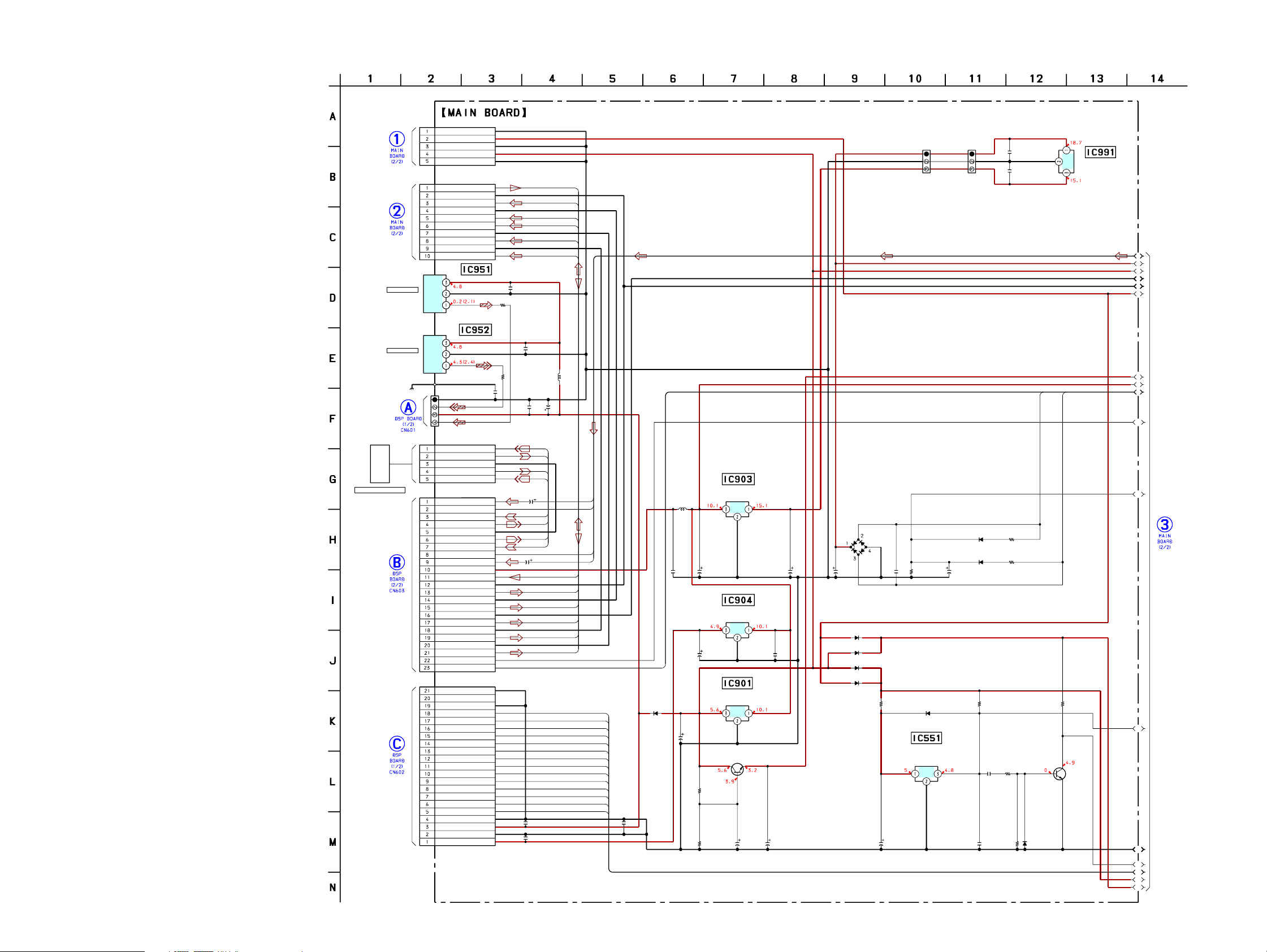
ST-S5
5-2. SCHEMATIC DIAGRAM – MAIN Board (1/2) –
(1/2)
CN5031
(Page 13)
(Page 13)
SYSTEM CONTROL 4
(TO TC-S3)
(Page 17)
(Page 16)
OPTICAL IN
(FROM CDP-S3)
OPTICAL IN
(CHASSIS)
(Page 16)
M(A)-GND
EVER+5V
D-GND
D+5V
MIC-SIG
MIC-GND
FL-OUT
FRONT-GND
FR-OUT
CENTER-OUT
CENTER-GND
SL-OUT
S-GND
SR-OUT
OPTICAL RECEIVER
VCC
GND
OUT
IC951
TORX178B
OPTICAL RECEIVER
VCC
GND
OUT
IC952
TORX178B
NO507
4P
REC OUT-R
PB-R
TC A-GND
PB-L
REC OUT-L
TUNER L-IN
VCD L-IN
TC L-IN
TC REC L-OUT
A-GND
TC REC R-OUT
TC R-IN
VCD R5-IN
TUNER R-IN
A+10V
MIC-IN
A-GND
FL-OUT
F-GND
FR-OUT
A-GND
LS-OUT
S-GND
RS-OUT
C-GND
C-OUT
LINE-MUTE
DBFB FEEDBACK
D-GND
D-OUT
D-GND
DSP-DECODE
DSP-CS
AMP-DATA
DSP-ACK
AMP-CLK
CODEC-SMUTE
AMP-LAT
DIR-Rx
DIG-Tx
DIR-XSTATE
DSP-Rx
DIR-CS
DIG-CLK
DIR-UNLOCK
D-GND
D+5V
A-GND
A+5V
CN5041
10P
(A-GND)
R952 L951
470
C916
10000p
CN510
CN508
23P
CN509
21P
5P
AA6
AA5
AA4
AA3
AA2
AA1
C955
10000p
R951
470
C957
10000p
220µH
C956
C964
10
10000p
50V
5P
BB1
BB2
BB3
BB4
C977
10
50V
BB3
BB4
BB1
BB2
C978
10 50V
C968
10000p
C970
10000p
DD1
DD2
DD3
DD4
AA6
AA5
AA4
AA2
AA1
AA3
NO901 NO991
3P 3P
+10V REGULATOR
IC903
L955
470µH
C966
10000p
C907
220
10V
DBFB FEEDBACK
D920
10000p
11ES2-NTA2
C902
470
10V
C971
E8
E7
E9
E6
E10
E5
E11
E4
E12
E3
E13
E2
E14
E1
NJM7810FA
IO
G
C905 C904 C952
470
16V
+5V REGULATOR
IC904
µPC7805AHF
IO
G
+7V REGULATOR
IC901
TA78057S
IO
G
Q902
2SC2001-K1K2
+3.3V REGULATOR
R911
220
R912
510
50V
3300
16V
C906
0.1
470
10
10V
D942 R942
D901
D3SBA20
C953
4700
25V
D922
11ES2
D903
11ES2
D904
11ES2
D923
11ES2
C551C918C903
10
50V
R943
0.1
3.3k
D551
1SS133T-72
RESET SIGNAL
GENERATOR
IC551
M51943BSL
IO
G
C941
10
50V
1SS133T 1k
R552R551
10k470
C991
0.1
C992
0.1
R941D941
1k1SS133T
I
+15V REGULATORG
IC991
O
NJM7815FA
1
2
3
4
5
6
7
8
9
AB20
AB21
10
11
(Page 13)
R555
4.7k
12
R554C553
47k0.1
Q551
2SC2603
RESET
SWITCH
D552R553C552
1SS133T47k0.1
13
14
15
16
17
1212
Page 13

5-3. SCHEMATIC DIAGRAM – MAIN Board (2/2) – • See page 20 for Waveforms.
(2/2)
CN506
15P
(AEP,UK)
ST-CLK
(E,AUS)
(AEP,UK)
11P
100
R957
ST-DIN
ST-DOUT
ST-CE
TUN
R958
R959
R961
R962
10k
4.7k
150
4.7k (MX)
RDS-DATA
*
1k
*
100
100
2.2k
2.2k
ST-MUTE
RDS-INT
R545
(AEP,UK)
(KR,AUS)
(MX)
R546
(KR,AUS)
STE
C909
D911
11ES2
-NTA2
100
50V
C961
0.1
JW95
E7
E8
STE
TUN
SIRCS
C962
10
50V
D902
11ES2-NTA2
(AEP,UK)
C915 D912
100
35V
R908
1k
R903
10
D945
1SS133T
C508
10
50V
R548
4.7k
R964
DD1
5.6k
DD4
R963
5.6k
C910
Q901
2SB734-3
-28V REGULATOR
C506
4.7
R558 R550 D944
50V 1M 100k 1SS133T
C510
4.7
50V
R541
47k
47k
R543
150
R545
*
R544
4.7k
C509
(E,AUS)
0.1
MTZJ-T72-30B
R539
100
R540
100
R542
R546
*
R904 R905
10
10k 100
50V
B
.6
-5
3
2
1
9
-7
D
-T
J
Z
T
M
R549
3.3k
Q503
BN1A4M
AC OFF
MUTING
R557
DRIVER
22k
E6
R538 R530
100 100
DSP-ACK
DSP-CS
DSP-DECODE
STEREO
TUNED
MODEL-IN
SPEC-IN
V-MUTE
AVSS
VREF
AVCC
AC-
CUT
R501
100
E9
ANTENNA
(AEP,UK)
(E,AUS)
CL
MC D0
COAXIAL
FM 75Ω
SUPPLIED WITH*
THE ASSEMBLED
BLOCK
FM/AM
TUNER
UNIT
*
FM
75Ω
AM
MC D1
CE
A+10V
TUNED
STEREO
L-CH
ANALOG-GND
R-CH
MUTE
D+5V
N.C
RDS-INT
RDS-DATA
1
2
3
4
5
6
7
8
9
10
11
(Page 12)
12
13
14
15
16
17
ST-S5
CN505
DD2
DD3
I-CLK
I-DAT
M-RESET
2
AB1
-7
1
3T
92
3
AB2
C937
R906
0.1
100
POWER KEY
D943
1SS133T
Q502
BN1A4M
MUTING
CONTROL
SWITCH
C942
470
6.3V
R532
47k
E2
E1
E3
E4
E5
0
0
0
0
0
0
0
0
0
0
0
1
1
1
1
1
3
4
5
6
7
3
3
3
3
3
5
5
5
5
5
R
R
R
R
R
X
EC
UTE
IR-R
COD
DIR-CS
D
-SM
DIR-XSTATE
TA
LK
-C
-DA
P-LAT
P
P
SIRCS
DIG-TX
AM
AM
AM
0
0
0
0
0
0
0
0
0
0
1
1
1
1
1
2
3
4
5
6
0
0
0
0
0
5
5
5
5
5
R
R
R
R
R
E11
E10
E12
E13
0
1
1
3
5
R
K
EY
ER KEY
W
IR-UNLOC
PO
D
DISPLAY K
-CLK
D
SP-RX
CNVSS
DIG
D
GN
0
0
1
7
0
5
R
k
0
1
E14
8
0
5
R
CC5 CC6
R556
47k
UTE
LINE-M
SYSTEM CONTROLLER
T
ESET
COU
XCIN
R
X
k
0
3
z
3
H
0
k
3
9
8
3
0
6
5
.7
0
R
2
1
3
5
R
1
0
5
X
p
p
8
5
.1
1
1
0
1
2
3
0
0
0
5
5
5
C
C
C
IC501
M30622MGA-A39FP
XOUT
XIN
VSS
z
H
M
6
1
2
0
5
X
C943
0.1
EX-IN
EX-LAT
EX-OUT
EX-CLK
0
0
0
0
0
0
1
1
1
8
7
6
2
2
2
5
5
5
R
R
R
R956
100
SS
V
SOFT-TEST
I
DS-INT
M
R
N
VCC
k
0
1
1
1
5
R
C504
0.1
C505
1000
6.3V
RDS-INT
TA
ATA
VCC
-CLK
DA
T D
EXP-LAT
EXP
EXP-IN
EXP-OU
UT
UTE
DS-DATA
T-M
T-DIN
S
ST-DO
ST-CE
R
0
0
1
2
1
5
R
(E,AUS)
1
2
0
0
5
5
JW
JW
RDS-DATA
0
0
1
3
1
5
R
ST-MUTE
S
0
0
1
4
1
5
R
ST-DIN
ST-DOUT
ST-CE
ST-CLK
ST-CLK
R524
47k
EPT901
C561
0.1
-USE
NO
R523
100
M-RESET
R522
M-RESET
NO-USE
NO-USE
NO-USE
NO-USE
LK
IIC DATA
IIC C
R518R516R515 R517
1001001k 100
I-DAT
I-CLK
10k
C562
10000p
CC2
CC3
CC4
CC1
C519
100p
R519
10k
R520
10k
C520
100p
D
S1
1S
CC1
CC2
CC3
CC4
CC5
CC6
I-CLK
I-DAT
JOG2-B
JOG2-A
JOG1-B
JOG1-A
VOLA
VOLB
M-RESET
I-DAT
I-CLK
KEY1
SIRCS
JOG2-B
JOG2-A
JOG1-B
JOG1-A
VOLA
VOLB
AB20
AB21
AB2
AB1
DBFB FEEDBACK
POWER KEY
EX-CLK
EX-LAT
EX-OUT
EX-IN
KEY1
R525
R529
R521
R965
100
R966
100
C972
C927C928
0.10.1
100
100
100
17P
VCD L-IN
CD A-GND
VCD R-IN
HAKO-GND
TC M-GND
TC M-GND
UNREG
TC D-GND
I2C-CLK
I2C-DATA
V-MUTE
MRESET
EVER+5V
CD D(M)-GND
CD D(M)-GND
AC-LOW
AC-LOW
CN502
19P
DISPLAY/STANDBY KEY
VF
VF
-VP
D-GND
JOG2-B
JOG2-A
JOG1-B
JOG1-A
VOLA
VOLB
RESET
IIC-DATA
IIC-CLK
KEY1
D+3.3V
D-GND
EVER+5V(SIRCS)
SIRCS
CN5042
9P
DBFB FEEDBACK
HAKO-GND
POWER KEY
EXP-CLK
EXP-LAT
EXP-OUT DATA
EXP-IN DATA
KEY0 TA
UNREG
CN5032
15P
JOG2-B(F-SELECT)
JOG2-A(F-SELECT)
JOG1-B(FUNCTION)
JOG1-A(FUNCTION)
VOLA
VOLB
AC HIGH
0.1
AC HIGH
AC LOW
AC LOW
VP
VF
VF
CT
CT
EPT902
CN503
10P
GND
TXD1/CAN'T USE
RTS1
NC
+5V
CLK1/SQ-CLK
RXD1/SQ-DATA-IN
CNVSS
RESET
GND
CN501
4P
D-GND
D+5V
IIC-CLK
IIC-DATA
(CHASSIS)
(CHASSIS)
(Page 19)
(Page 12)
(CHASSIS)
(FOR TEST)
(FOR TEST)
SYSTEM CONTROL 3
(FROM CDP-S3)
SYSTEM CONTROL 2
(TO TA-S7AV)
SYSTEM CONTROL 1
(TO TA-S7AV)
(Page
12)
1313
Page 14

ST-S5
5-4. PRINTED WIRING BOARD – MAIN Board – • See page 11 for Circuit Boards Location.
• Semiconductor
Location
Ref. No. Location
D551 D-4
D552 D-4
D901 C-8
D902 C-7
D903 E-4
D904 E-5
D911 C-6
D912 C-5
D913 C-5
D920 F-4
D921 E-5
D922 D-5
D923 D-5
D941 C-7
D942 C-7
D943 E-4
D944 E-3
D945 E-4
IC501 C-2
IC551 D-4
IC901 E-6
IC903 D-6
IC904 G-4
IC951 G-10
IC952 F-10
IC991 H-8
Q502 E-3
Q503 E-4
Q551 D-4
Q901 C-5
Q902 F-4
A
B
C
D
E
F
G
H
D
PANEL
BOARD
CN602
(Page 18)
1 2 3 4 5 6 7 8 9 10
ANTENNA
(E, AUS)
FM
(AEP, UK)
75Ω
AM
* SUPPLIED WITH
THE ASSEMBLED BLOCK
(AEP, UK)
R962
JW70
JW68
C962
R965
JW91
JW90
1
JW116
R963
JW92
R966
JW80
JW78
JW76
JW917
15
CN510
SYSTEM
CONTROL 4
(TO TC-S3)
R956
JW89
JW44
C964
NO507
A
CN5042
1
9
CN5041
1
10
JW79
JW77
JW71
JW69
4
DSP BOARD
CN601
JW81
EPT902
JW84
C956
JW954
JW98
JW107
JW87
L951
R951
JW88
C916
R952
C955
C957
JW83
CN505
JW97
IC952
3
1
IC951
3
1
1-680-695-
MAIN BOARD
R556
R542
R541
R530
R533
R534
R535
R536
R537
R538
R539
R540
R543
R545
R544
R546
(E, AUS)
CN502
JW209
JW208
JW207
JW206
JW205
JW204
JW203
JW202
JW201
JW19
JW35
R527
C509
JW21
R526
R501
JW956
R524
C943
C508
R502
R532
R503
JW957
C971
X501
R548
R504
JW16
JW15
JW14
C970
C561
IC501
JW503
JW96
R506
R505
C968
EPT901
R509
R507
R557
R531
C502
C510
JW17
R528
JW32
X502
R510
C501
JW18
(CHASSIS)
R516
R508
C506
JW13
CN509
C
R515
R514
(E, AUS)
R511
C504
C503
JW29
JW26
JW113
R558
R549
DSP BOARD
CN602
(Page 15)
R523
R513
C505
JW30
JW27
R550
R522
C562
JW50
R512
JW502
JW501
JW500
R521
Q551
D944
EE
Q502
Q503
JW28
JW93
(FOR TEST)
10 1
CN503
R525
JW41
JW42
JW40
R529
JW51
R517
R518
JW39
14
C918
E
R553
C942
D943
C552
IC551
R912
Q902
CN501
(FOR TEST)
1
3
D552
JW55
D945
C903
E
R911
JW67
JW918
D551
R551
31
JW38
IC904
C907
R552
C553
R554
R555
JW920
D920
JW43
R519
C520
C551
JW99
C906
C519
R520
D903
JW37
D904
L955
R906
JW952
C966
JW108
R905
D913
R904
D923
D922
JW34
Q901
ECB
R908
C910
D912
D921
C902
JW60
COAXIAL
JW921
C909
D911
R903
C937
JW118
C915
31
31
C905
JW115
JW971
CN5032
1
15
IC903
JW104
JW53
C972
C927
C928
C904
SYSTEM
CONTROL 1
(TO TA-S7AV)
JW47
JW25
(AEP, UK)
D902
D941
D942
JW959
JW958
R943
CN5031
NO901
R958
R959
C941
R942
R941
C953
15
1
3
R957
CN506
D901
4
1
JW119
JW94
JW106
JW100
C952
FM 75Ω
FM/AM TUNER UNIT *
C961
R961
R964
IC901
JW86
JW62
JW56
JW112
C977
CLP101
JW110
JW111
NO991
C978
JW64
C992
IC991
3
1
3
1
C991
JW65
JW117
JW85
CN508
JW75
DSP BOARD
B
CN603
(Page 15) (Page 15)
(INCLUDED IN MAIN BOARD)
(CHASSIS)
SYSTEM
CONTROL 2
(TO TA-S7AV)
OPTICAL IN
OPTICAL IN
(FROM CDP-S3)
11
(11)
IC952
IC951
SYSTEM
CONTROL 3
FROM
CDP-S3
1414
Page 15

5-5. PRINTED WIRING BOARD – DSP Board – • See page 11 for Circuit Boards Location.
ST-S5
1 2 3 4 5 6 7 8 9
J601
MD
A
IC609
OPTICAL
OUT
DSP BOARD
(COMPONENT SIDE)
DSP BOARD
(CONDUCTOR SIDE)
J602
SUB
WOOFER
OUT
OUT
L
R L
IN
R L R
VIDEO
(AUDIO)
IN
• Semiconductor
Location
Ref. No. Location
D601 C-8
D604 D-7
D605 D-7
D607 E-2
D608 E-2
D609 E-1
D610 E-1
IC601 C-4
IC609
IC602
R619
C651
E
Q602
R662
C634
R656
C650
13
C652
FB605
R664
R665
IC606
R649
CN602
D604
C648
C673
R687
R685
X601
R691
12
22
R644
C625
R686
R640
R646
R692
R684
JR622
R637
R638
R639
11 1
IC605
23
R647
R645
R648
R602
33
C642
C643
R642
C701
C604
44
34
C677
R636
R654
C601
C603
R611
R612
R613
R635
C740
C644
B
R743
R746
R756
R739
R757
R781
R780
R742
R779
R738
R735
IC608
C
R670
R671
R672
C628
R668
R669
R673
R678
36 25
37
48
C617
C618
C632
C627
1
R681
C629
12
24
IC604
13
C624
R667
R690
C626
C602
R689
R641
D
R706
R758
R760
R762
E
R765
R769
R772
F
G
R707
R713
R717
D610
D609
R715
D608
D607
(E, AUS)
R716
R761
R711
R712
R759
R643
IC607
C676
C675
C631
C630
120 91
C612
1
30
31 60
C606
R615
C736
C646
R653
R666
R658
R659
C653
C683
C682
C681
JR603
C732
C611
IC601
C657
C654
C607
R616
R657
R660
R661
R655
JR601
R617
R663
C610
R614
R618
IC603
R631
C649
R633
R632
90
61
C609
C608
(CHASSIS)
FB608
C721
R754
FB607
C735
R628
C615
C616
R680
1
C613
C738
R621
R620
R629
R630
Q612
E
A
4
CN601
R755
1-680-319-
MAIN
BOARD
NO507
(Page 14)
11
(11)
R650
C
C614
D605
C658
C656
FB604
C672
MAIN BOARD
R734
C674
CN509
C719
C655
C720
FB601
C647
C703
C671
C659
C645
C680
C690
C678
R651
C660
R610
C702
C636
C679
Q603
R652
C670
IC610
FB602
R608
C741
C637
R727
E
R695
C668
C661
R603
R604
R605
R606
R607
C742
C638
R728
C691
R777
R776
C669
R693
C712
R748
3
1
C664
D601
C662
R601
Q613
C635
C639
C684
R719
R725
R723
E
Q610
C689
R694
C667
C640
R729
E
R623
R688
JR621
R720
Q609
R724
C711
R747
Q601
C739
R771
E
C641
C717
C714
R750
E
C665
FB603
C666
R634
C622
C621
C620
R683
C730
R699
C685
C686
C723
R768
R775
C623
C731
R721
E
Q608
FB606
C633
C694
R778
R770
R773
R766
R763
R767
R774
R677
R679
C687
R703
C722
E
Q606
(E, AUS)
C713
R749
C725
R784
C619
C695
C693
C699
R674
R676
R696
C728
E
Q607
R675
R698
C724
C715
R752
R682
R701
C692
C727
C729
D606
R709
R731
C700
E
Q611
C704
R702
R697
C706
C716
R751
R733
R730
Q605
R700
Q604
C726
C733
EP603EP604
C709
C710
C705
C708
E
E
CN603
EP602
C707
JR620
1-680-319-
(CHASSIS)
MAIN
BOARD
CN508
(Page 14)
(CHASSIS)
11
(11)
B
IC602 C-6
IC603 E-4
IC604 C-2
IC605 D-3
IC606 E-7
IC607 F-2
IC608 C-2
IC609 B-6
IC610 C-7
Q601 C-8
Q602 F-6
Q603 F-7
Q604 E-9
Q605 D-9
Q606 G-8
Q607 G-9
Q608 E-8
Q609 F-8
Q610 F-8
Q611 C-9
Q612 E-6
Q613 D-8
(Page 14)
1515
Page 16

ST-S5
5-6. SCHEMATIC DIAGRAM – DSP Board (1/2) – • See page 20 for Waveforms. • See page 20 for IC Block Diagram.
CN602
21P
(CHASSIS)
IC602
IS61LV6416-15T
EP604
GND
(Page 12)
(Page 12)
C735
0.1
A+5V
A-GND
D+5V
D-GND
DIR-UNLOCK
DIG-CLK
DIR-CS
DSP-Rx
DIR-XSTATE
DIG-Tx
DIR-Rx
AMP-LAT
CODEC-SMUTE
AMP-CLK
DSP-ACK
AMP-DATA
DSP-CS
DSP-DECODE
D-GND
D-OUT
D-GND
CN601
4P
R755
100
R754
100
C721
220
10V
S-RAM
A9
A8
A7
A6
A5
A2
A4
A3
A19
A20
A32
A33
A34
C613
0.1
A28
A29
A30
A31
A12
A11
A10
A25
A26
A27
C6
C5
C4
C3
B1
B2
C2
B3
C1
D0
D1
A1
A13
C614
0.1
A24
A14
A15
A16
A17
A18
A23
A22
A21
E1
E2
R619
100
R620
100
A3
A4
A5
R621
100
G6
C608
0.1
A6
A7
A8
A9
A10
A11
A12
A13
C609
0.1
A14
A15
A16
A17
TP601
TP602
TP604
TP605
TP603
XTRST
TDO
MS
TCK
TDI
A19
A18
C738
0.001
TP621
PAGE0
A24
A23
A22
A21
A20
R631
100
C1
R632
C5
R633
C2
TP623
PAGE1
AUDIO DIGITAL
SIGNAL PROCESSOR
C610 C611
0.1 0.1
A28
A27
A26
A25
FB607
C616
220
10V
C615
0.1
CXD9617R
FB608
100
100
IC603
TC74HCT7007AF
R618
100
C606C607
A1
A2
0.10.1
IC601
A34
A33
A32
A31
A30
A29
LEVEL SHIFT
E1
100
100
R616
R617
E2
100
100
R614
R615
R630
100
R629
100
R628
100
C612 C739
0.1 0.001
C659
FB601
0
NJM2391DL1-26TE1
1
2
3
C657
1000p
R680
3.3k
Q612
FN1F4M
MUTING
CONTROL
SWITCH
C4
F3
C6
F2
C3
F1
D604
1SS355
R613
100
G4
100
G2
R612
100
G3
R611
R610
100
H7
100
H6
R608
100
H5
R607
100
H4
R606
JR622
G1
0
H3
100
H2
R605
100
H1
R604
R603
100
C604
0.1
R602
1k
C603
0.1
G5
C602
R601
100
+2.6V REGULATOR
C601
0.1
R623
10k
SWITCH
Q613
FA1A4M
RESET
0.01
C742
R771
10k
0.001
TP622
PLOCK
C740
0.1
R634
100
220
10V
OGI
IC610
D605
1SS355
C658
0.1
C645
220
10V
C644
0.1
R653
10k
R654C646
10k0.01
C736
0.1
DIGITAL
FILTER,
D/A CONVERTER
IC606
PCM1748E/2K
R656R655
10k10k
H3
H7
TP619
H2
FB605
0
FB604
0
220
10V
C647
220
10V
100
R657
100
R658
100
D4
R659
R662
100
Q602
2SC1623
+3.3V
REGULATOR
R663
470
N1
R651R652
470470
C643
0.001
TP614
TP615
TP618
TP617
TP611
C656
E2
E1
220
10V
100
100
R665
R666
C650C648
220
10V
N3
N2
R635
100
BCK
LRCK
D2
D3
BCK
R664
100
R649
470
R650
470
C642
0.001
A/D,D/A CONVERTER
100
R636
H3
C655
0.1
JR621
0
C654C653
0.010.1
R660
330
R661
0.1
330
C651
C652C649
0.10.1
N9
N8
N7
N6
N5
N4
AK4527
100
R637
H2
N10
330
330
330
330
330
330
R643
R644
R645
R646
R647
R648
IC605
R641
100
100
100
100
R640
R639
R638
TP616
DOUT
H1
H6
H5
H4
JR603
0
0.01
0.01
0.01
0.01
C641
C638
C639
C640
4
5
6
7
8
0.01
C637
C636
0.01
(Page
17)
R642
100
9
C635
0.1
10
11
12
13
14
15
16
17
18
19
1616
Page 17

5-7. SCHEMATIC DIAGRAM – DSP Board (2/2) – • See page 20 for Waveforms. • See page 20 for IC Block Diagram.
ST-S5
(Page
16)
1
2
3
4
5
JR601
0
6
7
8
FB602
0
Q601
2SD1387
+3.3V
REGULATOR
9
R692
C665
100
0.1
C664
C662
C660
220
10V
G1
G2
G3
G4
G5
G6
10
11
12
13
14
15
16
17
18
19
0.1
0.1
C661
220
10V
TP620
D601
RD3.9SB2
BCK
LRCK
DATA
TP612
TP613
100
R684
R685
100
R686
100
R687
100
R688
100
C624
R691
X601
13.5MHz
C625 C626
10p 10p
0.1
R690R667
1M100
0
R689
1k
F3
C623
220
10V
C622
C666
220
10V
N1
N2
N3
N4
N5
N6
N7
N8
N9
N10
C618
0.01
FB603
C621
0.01
C620
0.1
0.1
C617
0.1
C619
R677
5.6k
R679
4.7k
0.1
R681
33k
C667
C668
C669
C670
C671
C672
C673
C674
C675
C676
C677
C678
B3
R694
B2
R695
B1
C741
0.1
100
R683
DIGITAL AUDIO
INTERFACE RECEIVER
IC604
LC89056W-E
10 50V
10 50V
10 50V
10 50V
10 50V
10 50V
10 50V
10 50V
1 50V
1 50V
1 50V
10 50V
R682
100
C627
0.1
Q603
+5V
REGULATOR
R693
100
100
100
C679
0.1
1
3
M
M
F2
K9
(E,AUS)
C690
220
10V
M2
100
R676
R675
100
R678
10k
R669
R670R668
100
F1
E2
R778
1k
R674
100100
Q603
2SC1623
INPUT SELECT SWITCH,
GRAPHIC
EQUALIZER CONTROL,
ELECTRICAL VOLUME
IC607
M61512FP
100
K6
K8
K7
R776
10k
R777C691
10k0.1
R775
1k
10k
R774
J4
J2
1k
1k
1k
R770
R772
R773
L1 L2 L3 L4
R673
100
R672
100
R671
100
C628
0.1
K1
K3
K2
J3
J1
1k
1k
1k
1k
10k
1k
R768
R769
C682 C683C681C680
1 50V 1 50V1 50V10 50V
E1
R763
R765
R766
R767
R762
1k
FB606
47
C689
100
16V
R761
1k
1k
R760
1k
R759
1k
R758
100 16V
C687
100 16V
C686
C685
10
50V
50V
10
C684
D607
RB501V
D609
RB501V
(E,AUS)
INVERTER
IC608
M1
M2
M3
C633C632C629
220
0.10.1
10V
SN74LVU04APWR
D608
RB501V
D610
RB501V
R698
470k
R699
470k
C722
0.1
C692
C693
0.1
C694
0.1
C695 R696
0.1 1.8k
50V
R697
0.1
R702
R703
50V
L4
L3
L2
L1
C724
0.1
1.8k
1M
1M
C700
10
50V
C701 R719
1
50V
50V
50V
C704
2.2
50V
C725
10
50V
R711
C699
10
1k
50V
R712
R700
47k
10k
2SC1623
10k
2SC1623
R701
R715
C731C730
0.110
1k
R720
47k
R723C702
1k1
R724
47k
R727C703
1k1
R728
47k
R731
4.7k
R730
22k
R757
47k
C726
0.1
Q604
Q605
DBFB CONTROL/
FEED BACK SWITCH
1k
R716
47k
R707
47k
R706
47k
Q604,605
Q608
2SC3624
MUTING
Q609
2SC3624
MUTING
Q610
2SC3624
MUTING
Q611
2SC3624
MUTING
2SC3624
MUTING
C727
10
50V
Q606
R709 D606
Q607
2SC3624
MUTING
R779R780R781R756
47k47k47k47k
C631
0.01
C630
0.01
R713
00
R721
1k
R725
1k
R729
1k
R733
1k
K4
J5
K5
J6
50V
0.1
10
C728
C729
I2
1k
I6
I1
1k
R717
I4
I3
I5
D1
D0
C634
0.1
K1
K2
K3
K4
K5
K6
K7
K8
K9
JR620
0
R752
C710
10
C716
50V
J1
J2
J3
J4
J5
J6
220p
220p
C715
C709
10
R751
50V
R750
C708
10
220p
C714
50V
R749
C707
10
220p
C713
50V
100k
R748
C706
10
470p
C712
50V
470p
C711
C705
10
50V
C733
0.1
I1
I2
I3
I4
I5
I6
47k
47k
12k
12k
R747
100k
C720
220p
TP606
TP607
TP608
TP609
TP610
R746
10k
R743
10k
R742
15k
R739
15k
R738
1k
R735
1k
R734
1k
C717 C719 C718
0.1 0.1 NO MT
C732
0.1
FL
FR
SL
SR
C
DBFB FEEDBACK
OPTICAL
TRANSCEIVER
TOTX178A
TUNER L-IN
VCD L-IN
TC REC L-OUT
TC REC R-OUT
VCD R5-IN
TUNER R-IN
LINE-MUTE
TP624
A.GND
IC609
TC L-IN
TC R-IN
MIC-IN
FL-OUT
FR-OUT
LS-OUT
RS-OUT
A-GND
A+10V
A-GND
F-GND
A-GND
S-GND
C-GND
C-OUT
CN603
EP602C723
EP603
GND10
23P
(CHASSIS)
(Page 12)
J601
6P
L
VIDEO
(AUDIO)
IN
R
L
IN
R
MD
L
OUT
R
J602
1P
SUB
WOOFER
OUT
GND
(CHASSIS)
D.GND
OPTICAL
VCC
OUT
D.OUT
1717
Page 18

ST-S5
5-8. PRINTED WIRING BOARDS – PANEL Section – • See page 20 for Circuit Boards Location.
1 2 3 4 5 6 7 8 9 10
PANEL BOARD
A
S611
B
R623 R624 R625
S607
ENTER – PRESET TUNER MEMORY
R622
R621
S609S608
+
STEREO/MONO
R626
S610
R620
C
S606
– +
TUNING
(AEP, UK)
S612
D
PTY
S604S605
TUNER/BAND
R627
(AEP, UK)
S601 – 612
R619
C610
JW24
R638
R636
R634
R632
R630
R628
C649
C650
JW1
R603
JW8
JW10
R629
JW11
C666
CN602
D
C664
R639
R637
R635
R633
R631
R605
R604
MAIN BOARD
(Page 14)
C615
CN502
C614
C662
FL601
FLUORESCENT
INDICATOR
TUBE
JW31
JW33
JW36
JW57
R618
DISPLAY
CLOCK/TIMER
TIMER SELECT
S601
S602
S603
NO601
1
3
1-680-696-
(11)
SIRCS
BOARD
C101
IC101
3
1
R102
NO101
1
R101
3
1-680-697-
11
11
(11)
C601
C665
R602R601
C663
C603
C607
D601
JW602
C669
JW6
R677
JW601
IC601
C608
JW5
R617
R606
R607
X601
JW114
C605
C606
R608
C651
R616
JW3
C652
JW4
JW45
C653
C655
C654
C656
C657
C658
C659
C661
C660
• Semiconductor
Location
Ref. No. Location
D601 C-5
IC101 C-10
IC601 B-5
1818
Page 19

5-9. SCHEMATIC DIAGRAM – PANEL Section – • See page 20 for Waveform.
FL601
FLUORESCENT INDICATOR TUBE
ST-S5
STEREO/
MONO
TUNER MEMORY
PRESET
ENTER
TUNING
TUNER/BAND
TIMER SELECT
CLOCK/TIMER
C610
10
50V
(AEP,UK)
S612
PTY
R627
5.6k
31
32
33
34
35
36
37
38
39
40
41
43
44
45
46
47
R601
10k
C649
10000p
C663
10000p
C664
0.1
C601
10000p
C665
47
50V
C666
47
50V
R617
270
+
-
-
+
S611
S610 R626
S608 R624
S607 R623
S605 R621
S604 R620
S602 R618
3.9k
R625S609
2.7k
2.2k
1.5k
R622S606
1.2k
1k
820
R619S603
560
470
47
1
2
3
4
5
6
7
8
9
12
10
13
14
15
16
17
18
19
20
21
22
24
25
26
27
28
29
30
7
8
22
A
A
A
A23
A24
A25
A26
A27
A28
A29
A30
A31
A32
A33
VSS FOR IO
A34
A35
A36
A37
A38
R603
C650
10000p
VKK FOR VFT
MODE0
MODE1
E2
2A
2B
G
G
OD
M
JO
JO
10k
TP603
TP604
TP605
1k
1k
R637
R639
B2
B1
10k
R638
TP601
TP602
R602
10k
TP606
1k
R635
B3
10k
R636
A
A
A
A
B
A
1A
1B
L
L
G
G
O
O
V
V
JO
JO
TP607
1k
1k
R631
R633
B6
B5
B4
10k
10k
10k
R630
R632
R634
13
14
15
A
A
A
V
R
FO
D
D
V
TA
A
D
C CLK
I2C
I2
C614
220p
100
100
R629
1k
605
R
R604
B8
B7
10k
628
R
FT
16
17
18
19
20
21
10
11
12
A
A
A
DISPLAY CONTROLLER
MB90M407PF-G-102
G
G
LO
ALO
N
NA
A
R
R A
FO
FO
S
CC
S
Y0
KE
AV
AV
220p
C615
B9
R606
C667 C668
0.1 0.1
IC601
-BND
9
A
A
A
A6
KEY1
10k
10k
R607
3
4
A
A
A5
IO
R
FO
S
VS
2
1
1
2
A
A
G
G
TP608
C605
10000p
3
G
RESET
4
G
VCC FOR CPU
VSS FOR CPU
R608
10k
6
5
G
G
G10
G11
G12
G12
G12
XOUT
XIN
C603
0.1
14
15
16
17
18
19
20
21
22
24
25
26
27
28
29
30
31
32
33
34
35
36
37
38
39
40
41
43
44
45
46
5
6
100p
100p
651
C652
C
G7
G7
G8
G9
C607
100
6.3V
7
10
8
12
9
13
1
2
3
4
100p
C653
100
100p
100p
100p
100p
657
655
C
C656
C
C654
C606
10
50V
96
97
98
99
100p
C658
X601
4MHz
101
100p
100p
100p
100p
662
660
659
C
C661
C
C
R616
100k
DISP/STANDBY KEY
VF
VF
NO101
3P
GND
+5V
OUT
-VP
D-GND
JOG2-B
JOG2-A
JOG1-B
JOG1-A
VOLA
VOLB
RESET
IIC-DATA
IIC-CLK
KEY1
D+3.3V
D-GND
EVER+5V(SIRCS)
SIRCS
100
99
98
97
96
101
C608
0.1
DISPLAY
B1
B2
B3
B4
B5
B6
B7
B8
B9
C669
0.1
D601
1SS133T-72
R677
1k
S601
GND
+5V
OUT
NO601
3P
CN602
19P
(Page 13)
C101
47
16V
R101
47
R102
47
GP1U28X
REMOTE CONTROL
RECEIVER
IC101
1919
Page 20

ST-S5
• Waveforms
– MAIN Board –
1 IC501 qa (XCOUT)
30.5 µs
2 IC501 qd (XOUT)
2.6 Vp-p
2.7 Vp-p
– DSP Board –
1 IC601 9 (MCLK1), IC604 w; (XMCK),
wa (XOUT)
4 Vp-p
74.1 ns
2 IC601 qf (SCKOUT)
4.6 Vp-p
5 IC601 ws (KFSIO), IC604 qd (CKOUT)
4.4 Vp-p
88.6 ns
6 IC601 wk (LRCKI2), IC604 qg (LRCK)
3.9 Vp-p
• IC Block Diagrams
– DSP Board –
IC604 LC89056W-E
36
CE
37
38
CL
39XSEL
MODE0
MODE1
DOSEL0
DOSEL1
CKSEL0
CKSEL1
XMODE
MICROCOMPUTER
40
41
42DGND
43DVDD
44
45
46
47
48
INTERFACE
DI
DO
35
BPSYNC
ERROR
3334
DGND
ERR9P
31
SAMPLING
FREQUENCY
LOCK
DETECT
DATA
DEMODULATOR
INPUT
CIRCUIT
XSEL
VF
30
DETECT
F2
C BIT
F1
X’ TAL
TIMING
F0
252627282932
PLL
CSFLAG
PA/PB
DETECT
AUDIO
24
23
EMPHA
22
XIN
21
XOUT
20
XMCK
19 DVDD
18 DGND
17
XSTATE
16
DATAO
LRCK
15
BCK
14
CKOUT
13
62.5 ns
– PANEL Board –
1 IC601 id (XOUT)
250 ns
3.5 Vp-p
74.1 ns
3 IC601 ql (LRCKO), IC605 5 (LRCK),
IC606 3 (LRCK (I))
3.8 Vp-p
22.7 µs
4 IC601 w; (BCKO), IC605 4 (BCK),
IC606 1 (BCK (I))
3.6 Vp-p
354 ns
22.7 µs
7 IC601 wl (BCKI2), IC604 qf (BCK)
354 ns
8 IC606 qh (MCLK (I))
3.7 Vp-p
74.1 ns
4 Vp-p
IC605 AK4527
LOOP1
LOOP0/SDA/CDTI
44 43 42 41 40 39 38 37 36 35 34
1
SDOS
I2C
2
SMUTE
3
BICK
4
LRCK
5
SDTI1
6
SDTI2
7
SDTI3
8
SDTO
9
10
11
FORMAT
CONVERTER
12 13 14 15 16 17 18 19 20 21 22
DEM1
DAUX
DFS
1 2 3 4
DOUT
DISEL
DIF1/SCL/CCLK
DIF0/CSN
P/SN
MCLK
DZF1
AUDIO
INTERFACE
PDN
TVDD
DVSS
DVDD
DEM0
DINO
AVSS
ICKS2
AVDD
ICKS1
VREFH
CIRCUIT
OUTPUT
CIRCUIT
ICKS0
DINI
VCOM
INPUT
CAD1
CAD0
5
6
DIN2
DGND
33
DZF2
RIN+
32
RIN–
31
LIN+
30
29
LIN–
28
ROUT1
27
LOUT1
26
ROUT2
25
LOUT2
24
ROUT3
23
LOUT3
7
DVDD
8 9 10
R
VIN
LPF
11
12
AVDD
AGND
2020
Page 21

5-10. IC PIN FUNCTION DESCRIPTION
• MAIN BOARD IC501 M30622MGA-A39FP (SYSTEM CONTROLLER)
Pin No. Pin Name I/O Description
1 AMP-DATA O
2 AMP-CLK O
3 AMP-LAT O
4 SIRCS I
5 DIG-TX O
6 DSP-RX
7 DIG-CLK
8 GND —
9 CNVSS —
10 XCIN I
11 XCOUT O
12 RESET I
13 XOUT O
14 VSS —
15 XIN I
16 VCC —
17 NMI I
18 RDS-INT
19 ——
20 RDS-DATA
21 ST-MUTE O
22 ST-CE O
23 ST-DOUT O
24 ——
25 ST-DIN
26 ——
27 ST-CLK
28 ——
29 IIC CLK I/O
30 IIC DATA I/O
31 to 34 NO-USE —
35 to 40 ——
41 M-RESET O
42 to 50 ——
51 NO-USE —
52 to 57 ——
58 EXP-IN DATA
59 EXP-OUT DATA O
60 EXP-LAT O
61 EXP-CLK O
62 VCC —
63 SOFT-TEST
Serial data output to the M61512FP (IC607)
Serial data transfer clock signal output to the M61512FP (IC607)
Serial data latch pulse signal output to the M61512FP (IC607)
Remote control signal input from the remote control receiver (IC101)
Serial data output to the CXD9617R (IC601), digital audio interface receiver (IC604) and digital
filter (IC606)
I Serial data input from the digital audio interface receiver (IC604)
Serial data transfer clock signal output to the CXD9617R (IC601), digital audio interface receiver
O
(IC604) and digital filter (IC606)
Ground terminal
Not used
Sub system clock input terminal (32.768 kHz)
Sub system clock output terminal (32.768 kHz)
System reset signal input from the reset signal generator (IC551) “L”: reset
For several hundreds msec. after the power supply rises, “L” is input, then it changes to “H”
Main system clock output terminal (16 MHz)
Ground terminal
Main system clock input terminal (16 MHz)
Power supply terminal (+5V)
Non-maskable interrupt input terminal Fixed at “H” in this set
I Serial data transfer clock signal from the RDS decoder on the FM/AM tuner unit
Not used (open)
I Serial data input from the RDS decoder on the FM/AM tuner unit
Tuner muting on/off control signal output to the FM/AM tuner unit “L”: muting on
Chip enable signal output to the FM/AM tuner unit
Serial data output to the FM/AM tuner unit
Not used (open)
I Serial data input from the FM/AM tuner unit
Not used (open)
O Serial data transfer clock signal output to the FM/AM tuner unit
Not used (open)
Communication data reading clock signal input or transfer clock signal output with the display
controller (IC601) and CDP-S3
Communication data bus with the display controller (IC601) and CDP-S3
Not used
Not used (open)
Reset signal output to the display controller (IC601) “L”: reset
Not used (open)
Not used
Not used (open)
I Serial data input from the I/O expander in the TA-S7AV
Serial data output to the I/O expander in the TA-S7AV
Serial data latch pulse signal output to the I/O expander in the TA-S7AV
Serial data transfer clock signal output to the I/O expander in the TA-S7AV
Power supply terminal (+5V)
I Soft test output terminal Not used (open)
ST-S5
21
Page 22

ST-S5
Pin No. Pin Name I/O Description
64
65 to 70 ——
71 LINE-MUTE
72 ——
73 DISPLAY KEY I
74 POWER KEY I
75 DIR-UNLOCK
76 DIR-CS O
77 DIR-XSTATE
78 DIR-RX
79 CODEC-SMUTE O
80 DSP-ACK
81 DSP-CS
82 DSP-DECODE
83 to 86 ——
87 STEREO I
88 TUNED I
89 to 91 ——
92 MODEL-IN
93
94 ——
95 V-MUTE O
96
97 ——
98
99 AVCC —
100 AC-CUT I
VSS — Ground terminal
Not used (open)
O Audio line muting on/off control signal output to the audio line circuit “L”: muting on
Not used (open)
DISPLAY switch (S601) input terminal
Power on/off switch in the TA-S7AV input terminal
I PLL lock error and data error flag input from the digital audio interface receiver (IC604)
Chip enable signal output to the digital audio interface receiver (IC604)
I Source clock switching monitor input from the digital audio interface receiver (IC604)
I Read data input from the digital audio interface receiver (IC604)
Soft muting on/off control signal output to the A/D, D/A converter (IC605) “L”: muting on
I Acknowledge signal input from the CXD9617R (IC601)
O Chip select signal output to the CXD9617R (IC601)
O Decode signal input from the CXD9617R (IC601)
Not used (open)
FM stereo detection signal input from the FM/AM tuner unit “L”: stereo
Tuning detection signal input from the FM/AM tuner unit “L”: tuned
Not used (open)
I Model setting terminal
SPEC-IN I Specification setting terminal
Not used (open)
Video muting on/off control signal output terminal “L”: muting on Not used (open)
AVSS — Ground terminal
Not used (open)
VREF
I
Reference voltage (+5V) input terminal
Power supply terminal (+5V)
AC cut on/off detection signal input from the reset signal generator (IC551)
“L”: AC cut on, “H”: AC cut off or checked
22
Page 23

• DSP BOARD IC601 CXD9617R (AUDIO DIGITAL SIGNAL PROCESSOR)
Pin No. Pin Name I/O Description
1
2
3
4
5 VDDI —
6
7
8 VSS —
9
10
11
12
13
14
15
16 VDDE —
17
18
19
20
21
22
23 to 25 SDO1 to SDO3 O
26
27
28
29
30
31
32
33
34
35
36
37
38
39
40
41
42
43
44 CS0 O
45
46
47
VSS —
XRST I
EXTIN I
FS2 I
FS1 I
PLOCK O
MCLK1 I
VDDI —
VSS —
MCLK2 O
MS I
SCKOUT O
LRCKI1 I
BCKI1 I
SDI1 I
LRCKO O
BCKO O
VSS —
KFSIO I
SDO4 O
SPDIF O
LRCKI2 I
BCKI2 I
SDI2 I
VSS —
HACN O
HDIN I
HCLK I
HDOUT O
HCS I
SDCLK O
CLKEN O
RAS O
VDDI —
VSS —
CAS O
DQM O
WE0 O
VDDE —
WMD1 I
Ground terminal
Reset signal input from the M61512FP (IC607) “L”: reset
Master clock signal input terminal Not used (fixed at “L”)
Sampling frequency selection signal input terminal Not used (fixed at “L”)
Power supply terminal (+2.6V)
Sampling frequency selection signal input terminal Not used (fixed at “L”)
Internal PLL lock signal output terminal Not used (open)
Ground terminal
Oscillation clock signal input from the digital audio interface receiver (IC604)
Power supply terminal (+2.6V)
Ground terminal
Oscillation clock signal output terminal Not used (open)
Master/slave selection signal input terminal “L”: slave, “H”: master (fixed at “L” in this set)
Internal system clock signal output to the digital filter (IC606)
L/R sampling clock signal (44.1 kHz) input terminal Not used (open)
Power supply terminal (+3.3V)
Bit clock signal (2.8224 MHz) input terminal Not used (open)
Audio serial data input from the D/A, A/D converter (IC605)
L/R sampling clock signal (44.1 kHz) output to the D/A, A/D converter (IC605) and digital filter
(IC606)
Bit clock signal (2.8224 MHz) output to the D/A, A/D converter (IC605) and digital filter (IC606)
Ground terminal
Audio clock signal input from the digital audio interface receiver (IC604)
Audio serial data output to the A/D, D/A converter (IC604)
Audio serial data output to the digital filter (IC606)
S/PIDF signal output terminal Not used (open)
L/R sampling clock signal (44.1 kHz) input from the digital audio interface receiver (IC604)
Bit clock signal (2.8224 MHz) input from the digital audio interface receiver (IC604)
Audio serial data input from the digital audio interface receiver (IC604)
Ground terminal
Acknowledge signal output to the system controller (IC501)
Write data input from the system controller (IC501)
Clock signal input from the system controller (IC501)
Read data output to the system controller (IC501)
Chip select signal input from the system controller (IC501)
Clock signal output terminal Not used (open)
Clock enable signal output terminal Not used (open)
Row address strobe signal input terminal Not used (open)
Power supply terminal (+2.6V)
Ground terminal
Column address strobe signal output terminal Not used (open)
Output terminal of data input/output mask Not used (open)
Chip select signal output to the S-RAM (IC602)
Write enable signal output to the S-RAM (IC602)
Power supply terminal (+3.3V)
S-RAM wait mode setting terminal Fixed at “H” in this set
ST-S5
23
Page 24

ST-S5
Pin No. Pin Name I/O Description
48
49
50
51
52, 53
54
55
56
57
58
59
60
61
62, 63
64 to 66
67
68
69
70
71
72 to 75
76
77 to 80
81
82 to 85
86
87
88
89
90
91
92 to 97
98, 99
100
101
102 to 105 D5 to D2 I/O
106
107, 108
109, 110
111
112
113
114, 115
116
117 to 119 VSS —
120
VSS —
WMD0 I
PAGE2 O
VSS —
PAGE1, PAGE0 O
BOOT I
BTACT I
BST I
MOD1 I
MOD0 I
EXLOCK I
VDDI —
VSS —
A17, A16 O
A15 to A13 O
GP10 O
DECODE O
AUDIO I
VDDI —
VSS —
D15 to D12 I/O
VDDE —
D11 to D8 I/O
VSS —
A9, A12 to A10 O
TDO O
TMS I
XTRST I
TCK I
TDI I
VSS —
A8 to A3 O
D7, D6 I/O
VDDI —
VSS —
VDDE —
D1, D0 I/O
A2, A1 O
VSS —
A0 O
PM I
SDI3, SDI4 I
SYNC I
VDDI —
Ground terminal
S-RAM wait mode setting terminal Fixed at “L” in this set
Page selection signal output terminal Not used (open)
Ground terminal
Page selection signal output terminal Not used (open)
Boot mode control signal output terminal Not used (fixed at “L”)
Boot mode state display signal output terminal Not used (open)
Boot trap signal input from the M61512FP (IC607)
PLL input frequency select terminal “L”: 384fs, “H”: 256fs (fixed at “H” in this set)
Mode setting terminal “L”: single chip mode, “H”: use prohibition (fixed at “L” in this set)
PLL lock error and data error flag input from the digital audio interface receiver (IC604)
Power supply terminal (+2.6V)
Ground terminal
Address signal output terminal Not used (open)
Address signal output to the S-RAM (IC602)
L/R sampling clock signal (44.1 kHz) output to the D/A, A/D converter (IC605) and digital filter
(IC606)
Decode signal output to the system controller (IC501)
Bit 1 input terminal of channel status from the digital audio interface receiver (IC604)
Power supply terminal (+2.6V)
Ground terminal
Two-way data bus with the S-RAM (IC602)
Power supply terminal (+3.3V)
Two-way data bus with the S-RAM (IC602)
Ground terminal
Address signal output to the S-RAM (IC602)
Simple emulation data output terminal Not used (open)
Simple emulation data input start/end detection signal input terminal Not used (open)
Simple emulation asychronous break input terminal Not used (open)
Simple emulation clock signal input terminal Not used (open)
Simple emulation data input terminal Not used (open)
Ground terminal
Address signal output to the S-RAM (IC602)
Two-way data bus with the S-RAM (IC602)
Power supply terminal (+2.6V)
Ground terminal
Two-way data bus with the S-RAM (IC602)
Power supply terminal (+3.3V)
Two-way data bus with the S-RAM (IC602)
Address signal output to the S-RAM (IC602)
Ground terminal
Address signal output to the S-RAM (IC602)
PLL reset signal input from the M61512FP (IC607) “L”: reset
Audio serial data input terminal Not used (fixed at “L”)
Synchronous/asychronous selection signal input terminal
“L”: Synchronous, “H”: asynchronous (fixed at “H” in this set)
Ground terminal
Power supply terminal (+2.6V)
24
Page 25

• DSP BOARD IC604 LC89056W-E (DIGITAL AUDIO INTERFACE RECEIVER)
Pin No. Pin Name I/O Description
1
2 DOUT O
3 DIN0 I
4 DIN1 I
5 DIN2 I
6DGND—
7DVDD—
8RI
9 VIN I
10 LPF O
11 AVDD —
12 AGND —
13 CKOUT O
14 BCK O
15
16
17
18
19
20
21
22
23
24
25 CSFLAG O
26 to 28 F0 to F2 O
29 VF O
30
31
32
33
34 ERROR O
35
36
37
38
39
40
41
42
43
44
45
46
47
48
DISEL I
LRCK O
DATAO O
XSTATE O
DGND —
DVDD —
XMCK O
XOUT O
XIN I
EMPHA O
AUDIO O
DVDD —
DGND —
ERR9P O
BPSYNC O
DO O
DI I
CE I
CL I
XSEL I
MODE0 I
MODE1 I
DGND —
DVDD —
DOSEL0 I
DOSEL1 I
CKSEL0 I
CKSEL1 I
XMODE I
Selection terminal of data input terminal Fixed at “L” in this set
Digital data output to the optical transceiver (IC609)
Digital data input from the optical receiver (IC952) (for CDP-S3)
Digital data input from the optical receiver (IC951) (for external input)
Digital data input terminal Not used (fixed at “L”)
Ground terminal (digital system)
Power supply terminal (+3.3V) (digital system)
VCO gain control input terminal
VCO free run frequency setting input terminal
PLL loop filter setting output terminal
Power supply terminal (+3.3V) (analog system)
Ground terminal (analog system)
Audio clock signal output to the CXD9617R (IC601)
Bit clock signal (2.8224 MHz) output to the CXD9617R (IC601)
L/R sampling clock signal (44.1 kHz) output to the CXD9617R (IC601)
Audio serial data output to the CXD9617R (IC601)
Source clock switching monitor output to the system controller (IC501)
Ground terminal (digital system)
Power supply terminal (+3.3V) (digital system)
Oscillation clock signal output to the CXD9617R (IC601)
System clock output terminal (13.5 MHz)
System clock input terminal (13.5 MHz)
Emphasis information of channel status output terminal Not used (open)
Bit 1 output terminal of channel status to the CXD9617R (IC601)
Top 40 bit renovation flag output terminal of channel status Not used (open)
Input frequency calculation result output terminal Not used (open)
Validity flag output terminal Not used (open)
Power supply terminal (+3.3V) (digital system)
Ground terminal (digital system)
Nine times continuance data transmission error flag output terminal Not used (open)
Non-PCM burst and preamble sync signal output terminal Not used (open)
PLL lock error and data error flag output to the system controller (IC501)
Read data output to the system controller (IC501)
Write data input from the system controller (IC501)
Chip enable signal input from the system controller (IC501)
Clock signal input from the system controller (IC501)
Selection input terminal of vibrator frequency terminal Fixed at “H” in this set
Mode setting input terminal Fixed at “H” in this set
Mode setting input terminal Fixed at “H” in this set
Ground terminal (digital system)
Power supply terminal (+3.3V) (digital system)
Output data format selection signal input terminal Fixed at “L” in this set
Output data format selection signal input terminal Fixed at “L” in this set
Output clock selection signal input terminal Fixed at “L” in this set
Output clock selection signal input terminal Fixed at “L” in this set
System reset signal input from the M61512FP (IC607)
ST-S5
25
Page 26

ST-S5
• DSP BOARD IC605 AK4527 (A/D, D/A CONVERTER)
Pin No. Pin Name I/O Description
1
2 I2C I
3 SMUTE I
4 BICK I
5 LRCK I
6 to 8 SDTI1 to SDIT3 I
9 SDTO O
10 DAUX I
11
12
13
14
15
16
17
18 to 20 ICKS2 to ICKS0 I
21, 22
23
24
25
26
27
28
29
30
31
32
33
SDOS I
DFS I
DEM1 I
DEM0 I
TVDD —
DVDD —
DVSS —
PDN I
CAD1, CAD0 I
LOUT3 O
ROUT3 O
LOUT2 O
ROUT2 O
LOUT1 O
ROUT1 O
LIN– I
LIN+ I
RIN– I
RIN+ I
DZF2 O
Audio serial data source selection signal input terminal
“L”: internal ADC output, “H”: DAUX input (fixed at “L” in this set)
Serial control mode selection signal input terminal “L”: 3-wire serial, “H”: I2C bus
Soft muting on/off signal input from the system controller (IC501) “L”: muting on
Bit clock signal (2.8224 MHz) input from the CXD9617R (IC601)
L/R sampling clock (44.1 kHz) signal input from the CXD9617R (IC601)
Audio serial data input from the CXD9617R (IC601)
Audio serial data output to the CXD9617R (IC601)
Audio serial data input terminal Not used (fixed at “L”)
Double speed sampling mode signal input terminal
“L”: normal speed, “H”: double speed (fixed at “L” in this set)
De-emphasis signal input terminal Fixed at “L” in this set
De-emphasis signal input terminal Fixed at “H” in this set
Power supply terminal (+5V) (for output buffer )
Power supply terminal (+5V) (digital system)
Ground terminal (digital system)
Power down and reset signal input from the M61512FP (IC607) “L”: power down and reset
Input clock signal selection terminal Fixed at “L” in this set
Chip address signal input terminal Not used (fixed at “L”)
Analog signal output for center to the M61512FP (IC607)
Analog signal output for sub woofer to the M61512FP (IC607)
Analog signal output for surround L-ch to the M61512FP (IC607)
Analog signal output for surround R-ch to the M61512FP (IC607)
Analog signal output for front L-ch to the M61512FP (IC607)
Analog signal output for front R-ch to the M61512FP (IC607)
L-ch analog signal negative input from the M61512FP (IC607)
L-ch analog signal positive input from the M61512FP (IC607)
R-ch analog signal negative input from the M61512FP (IC607)
R-ch analog signal positive input from the M61512FP (IC607)
Zero input detection terminal Not used (open)
26
34
35
36
37
38
39
40
41
42
43, 44
VCOM O
VREFH I
AVDD —
AVSS —
DZF1 O
MCLK I
P/S I
DIF0 I
DIF1 I
LOOP0, LOOP1 I
Common voltage output terminal
Large external capacitor is used to reduce power supply noise
Reference voltage (+5V) input terminal
Power supply terminal (+5V) (analog system)
Ground terminal (analog system)
Zero input detection terminal Not used (open)
Master clock signal input from the CXD9617R (IC601)
Parallel/serial selection signal input terminal
“L”: serial control mode, “H”: parallel control mode (fixed at “H” in this set)
Audio data interface format terminal Fixed at “L” in this set
Audio data interface format terminal Fixed at “H” in this set
Loop back mode setting terminal Fixed at “L” in this set
Page 27

• PANEL BOARD IC601 MB90M407PF-G-102-BND (DISPLAY CONTROLLER)
Pin No. Pin Name I/O Description
1 to 6 G6 to G1 O
7 to 10 A1 to A4 O
11 VSS FOR IO —
12 to 22 A5 to A15 O
23 VDD FOR VFT —
24 to 41 A16 to A33 O
42 VSS FOR IO —
43 to 47 A34 toA38 O
48 VKK FOR VFT —
49 MODE0 —
50 MODE1 —
51 MODE2 —
52 JOG2B I
53 JOG2A I
54 JOG1B I
55 JOG1A I
56 VOLA I
57 VOLB I
58, 59 ——
60 I2C DATA I/O
61 I2C CLK I/O
62
63
64 KEY0 I
65 KEY1 I
66 to 76 ——
77 RESET I
78 to 80 ——
81 VSS FOR CPU
82 XIN I
83 XOUT O
84 VCC FOR CPU
85 to 91 ——
92 to 94 G12 O
95 to 98 G11 to G8 O
99, 100 G7 O
AVCC FOR
ANALOG
AVSS FOR
ANALOG
Grid drive signal output to the fluorescent indicator tube (FL601)
Segment drive signal output to the fluorescent indicator tube (FL601)
Ground terminal (for I/O)
Segment drive signal output to the fluorescent indicator tube (FL601)
Power supply terminal (+3.3V) (for VFT)
Segment drive signal output to the fluorescent indicator tube (FL601)
Ground terminal (for I/O)
Segment drive signal output to the fluorescent indicator tube (FL601)
Power supply terminal (–28V) (for VFT)
Chip mode selection terminal Not used (fixed at “H”)
Chip mode selection terminal Not used (fixed at “H”)
Chip mode selection terminal Not used (fixed at “L”)
Jog dial pulse input from the rotary encoder (for sound) in the TA-S7AV (B phase input)
Jog dial pulse input from the rotary encoder (for sound) in the TA-S7AV (A phase input)
Jog dial pulse input from the rotary encoder (for function) in the TA-S7AV (B phase input)
Jog dial pulse input from the rotary encoder (for function) in the TA-S7AV (A phase input)
Jog dial pulse input from the rotary encoder (for volume) in the TA-S7AV (A phase input)
Jog dial pulse input from the rotary encoder (for volume) in the TA-S7AV (B phase input)
Not used (open)
Communication data bus with the system controller (IC501) and CDP-S3
Communication data reading clock signal input or transfer clock signal output with the system
controller (IC501) and CDP-S3
—
Power supply terminal (+3.3V) (for analog)
—
Ground terminal (for analog)
Key input terminal (A/D input) CLOCK/TIMER, TIMER SELECT, TUNER/BAND, TUNING
+/–, ENTER, PRESET +/–, TUNER MEMORY, STEREO/MONO, PTY (S602 to S612) keys
input PTY (S612) key: Used for the AEP and UK models only
Key input terminal for TA-S7AV (A/D input)
Not used (open)
Reset signal input from the system controller (IC501) “L”: reset
Not used (open)
— Ground terminal (for CPU)
System clock input terminal (4 MHz)
System clock output terminal (4 MHz)
— Power supply terminal (+3.3V)
Not used (open)
Grid drive signal output to the fluorescent indicator tube (FL601)
Grid drive signal output to the fluorescent indicator tube (FL601)
Grid drive signal output to the fluorescent indicator tube (FL601)
ST-S5
27
Page 28

ST-S5
SECTION 6
EXPLODED VIEWS
NOTE:
• -XX and -X mean standardized parts, so they
may have some difference from the original
one.
• Color Indication of Appearance Parts
Example:
KNOB, BALANCE (WHITE) . . . (RED)
↑↑
Parts Color Cabinet's Color
• Abbreviation
AUS : Australian model
KR : Korean model
MX : Mexican model
6-1. COVER, FRONT PANEL SECTION
7
• Items marked “*” are not stocked since they
are seldom required for routine service. Some
delay should be anticipated when ordering
these items.
• The mechanical parts with no reference number in the exploded views are not supplied.
8
#2
1
4
6
5
5
3
AEP, UK
7
5
2
#1
Ref. No. Part No. Description Remark
1 X-4953-451-1 PANEL ASSY (ST), FRONT (AEP, UK)
1 X-4953-452-1 PANEL ASSY (ST), FRONT (KR, MX, AUS)
2 1-773-114-11 WIRE (FLAT TYPE) (19 CORE)
3 4-232-351-01 FILTER (FL)
4 1-680-697-11 SIRCS BOARD
5 4-951-620-01 SCREW (2.6X8), +BVTP
28
Ref. No. Part No. Description Remark
6 A-4476-267-A PANEL BOARD, COMPLETE (AEP, UK)
6 A-4476-269-A PANEL BOARD, COMPLETE (KR, MX, AUS)
7 3-363-099-21 SCREW (CASE 3 TP2)
8 4-233-134-31 COVER
#1 7-685-646-79 SCREW +BVTP 3X8 TYPE2 N-S
#2 7-685-871-01 SCREW +BVTT 3X6 (S)
Page 29

6-2. CHASSIS SECTION
54
ST-S5
56
55
#1
57
#1
A
51
not supplied
53
63
not supplied
(Including A)
not supplied
#1
#1
#1
#1
58
52
#1
#1
59
61
60
62
Ref. No. Part No. Description Remark
* 51 4-924-098-01 HOLDER, PC BOARD
52 A-2007-939-A MAIN BOARD, COMPLETE (MX)
52 A-4476-193-A MAIN BOARD, COMPLETE (AEP, UK)
52 A-4476-203-A MAIN BOARD, COMPLETE (KR, AUS)
53 A-4476-199-A DSP BOARD, COMPLETE (AEP, UK)
53 A-4476-646-A DSP BOARD, COMPLETE (MX)
53 A-4726-352-A DSP BOARD, COMPLETE (KR, AUS)
54 1-757-599-11 WIRE (FLAT TYPE) (21 CORE)
55 1-757-600-11 WIRE (FLAT TYPE) (23 CORE)
56 1-757-629-11 CORD (WITH CONNECTOR) 5P
57 1-757-631-11 CORD (WITH CONNECTOR) 20P
58 1-757-630-11 CORD (WITH CONNECTOR) 19P
Ref. No. Part No. Description Remark
59 4-232-327-01 PANEL (ST), BACK (AEP, UK)
59 4-232-327-11 PANEL (ST), BACK (AUS)
59 4-232-327-41 PANEL (ST), BACK (MX)
59 4-232-327-91 PANEL (ST), BACK (KR)
60 1-769-940-11 WIRE (FLAT TYPE) (11 CORE) (KR, MX, AUS)
60 1-773-004-11 WIRE (FLAT TYPE) (15 CORE) (AEP, UK)
61 1-693-529-11 TUNER PACK (FM/AM) (AEP, UK)
61 1-693-531-71 TUNER PACK (FM/AM) (MX, AUS)
61 1-693-538-11 TUNER PACK (FM/AM) (KR)
62 4-965-822-01 FOOT
63 3-970-608-01 SUMITITE (B3), +BV
#1 7-685-646-79 SCREW +BVTP 3X8 TYPE2 N-S
29
Page 30

ST-S5
DSP
SECTION 7
ELECTRICAL PARTS LIST
NOTE:
• Due to standardization, replacements in the
parts list may be different from the parts specified in the diagrams or the components used
on the set.
• -XX and -X mean standardized parts, so they
may have some difference from the original
one.
• RESISTORS
All resistors are in ohms.
METAL: Metal-film resistor.
METAL OXIDE: Metal oxide-film resistor.
F: nonflammable
• Abbreviation
AUS : Australian model
KR : Korean model
MX : Mexican model
Ref. No. Part No. Description Remark Ref. No. Part No. Description Remark
A-4476-199-A DSP BOARD, COMPLETE (AEP, UK)
A-4476-646-A DSP BOARD, COMPLETE (MX)
A-4726-352-A DSP BOARD, COMPLETE (KR, AUS)
********************
< CAPACITOR >
C601 1-164-156-11 CERAMIC CHIP 0.1uF 25V
C602 1-162-970-11 CERAMIC CHIP 0.01uF 10% 25V
C603 1-164-156-11 CERAMIC CHIP 0.1uF 25V
C604 1-164-156-11 CERAMIC CHIP 0.1uF 25V
C606 1-164-156-11 CERAMIC CHIP 0.1uF 25V
C607 1-164-156-11 CERAMIC CHIP 0.1uF 25V
C608 1-164-156-11 CERAMIC CHIP 0.1uF 25V
C609 1-164-156-11 CERAMIC CHIP 0.1uF 25V
C610 1-164-156-11 CERAMIC CHIP 0.1uF 25V
C611 1-164-156-11 CERAMIC CHIP 0.1uF 25V
C612 1-164-156-11 CERAMIC CHIP 0.1uF 25V
C613 1-164-156-11 CERAMIC CHIP 0.1uF 25V
C614 1-164-156-11 CERAMIC CHIP 0.1uF 25V
C615 1-164-156-11 CERAMIC CHIP 0.1uF 25V
C616 1-126-934-11 ELECT 220uF 20% 10V
C617 1-164-156-11 CERAMIC CHIP 0.1uF 25V
C618 1-162-970-11 CERAMIC CHIP 0.01uF 10% 25V
C619 1-164-156-11 CERAMIC CHIP 0.1uF 25V
C620 1-164-156-11 CERAMIC CHIP 0.1uF 25V
C621 1-162-970-11 CERAMIC CHIP 0.01uF 10% 25V
C622 1-164-156-11 CERAMIC CHIP 0.1uF 25V
C623 1-126-934-11 ELECT 220uF 20% 10V
C624 1-164-156-11 CERAMIC CHIP 0.1uF 25V
C625 1-162-915-11 CERAMIC CHIP 10PF 0.5PF 50V
C626 1-162-915-11 CERAMIC CHIP 10PF 0.5PF 50V
C627 1-164-156-11 CERAMIC CHIP 0.1uF 25V
C628 1-164-156-11 CERAMIC CHIP 0.1uF 25V
C629 1-164-156-11 CERAMIC CHIP 0.1uF 25V
C630 1-162-970-11 CERAMIC CHIP 0.01uF 10% 25V
C631 1-162-970-11 CERAMIC CHIP 0.01uF 10% 25V
C632 1-164-156-11 CERAMIC CHIP 0.1uF 25V
C633 1-126-934-11 ELECT 220uF 20% 10V
C634 1-164-156-11 CERAMIC CHIP 0.1uF 25V
C635 1-164-156-11 CERAMIC CHIP 0.1uF 25V
C636 1-162-970-11 CERAMIC CHIP 0.01uF 10% 25V
C637 1-162-970-11 CERAMIC CHIP 0.01uF 10% 25V
C638 1-162-970-11 CERAMIC CHIP 0.01uF 10% 25V
C639 1-162-970-11 CERAMIC CHIP 0.01uF 10% 25V
• Items marked “*” are not stocked since they
are seldom required for routine service.
Some delay should be anticipated when ordering these items.
• SEMICONDUCTORS
In each case, u: µ, for example:
uA. . : µA. . uPA. . : µPA. .
uPB. . : µPB. . uPC. . : µPC. .
uPD. . : µPD. .
• CAPACITORS
uF: µF
• COILS
uH: µH
C640 1-162-970-11 CERAMIC CHIP 0.01uF 10% 25V
C641 1-162-970-11 CERAMIC CHIP 0.01uF 10% 25V
C642 1-162-971-11 CERAMIC CHIP 0.001uF 10% 50V
C643 1-162-971-11 CERAMIC CHIP 0.001uF 10% 50V
C644 1-164-156-11 CERAMIC CHIP 0.1uF 25V
C645 1-126-934-11 ELECT 220uF 20% 10V
C646 1-162-970-11 CERAMIC CHIP 0.01uF 10% 25V
C647 1-126-934-11 ELECT 220uF 20% 10V
C648 1-126-934-11 ELECT 220uF 20% 10V
C649 1-164-360-11 CERAMIC CHIP 0.1uF 16V
C650 1-126-934-11 ELECT 220uF 20% 10V
C651 1-164-360-11 CERAMIC CHIP 0.1uF 16V
C652 1-164-360-11 CERAMIC CHIP 0.1uF 16V
C653 1-162-970-11 CERAMIC CHIP 0.01uF 10% 25V
C654 1-162-970-11 CERAMIC CHIP 0.01uF 10% 25V
C655 1-164-360-11 CERAMIC CHIP 0.1uF 16V
C656 1-126-934-11 ELECT 220uF 20% 10V
C657 1-162-971-11 CERAMIC CHIP 0.001uF 10% 50V
C658 1-164-156-11 CERAMIC CHIP 0.1uF 25V
C659 1-126-934-11 ELECT 220uF 20% 10V
C660 1-126-934-11 ELECT 220uF 20% 10V
C661 1-126-934-11 ELECT 220uF 20% 10V
C662 1-164-156-11 CERAMIC CHIP 0.1uF 25V
C664 1-164-156-11 CERAMIC CHIP 0.1uF 25V
C665 1-164-156-11 CERAMIC CHIP 0.1uF 25V
C666 1-126-934-11 ELECT 220uF 20% 10V
C667 1-126-964-11 ELECT 10uF 20% 50V
C668 1-126-964-11 ELECT 10uF 20% 50V
C669 1-126-964-11 ELECT 10uF 20% 50V
C670 1-126-964-11 ELECT 10uF 20% 50V
C671 1-126-964-11 ELECT 10uF 20% 50V
C672 1-126-964-11 ELECT 10uF 20% 50V
C673 1-126-964-11 ELECT 10uF 20% 50V
C674 1-126-964-11 ELECT 10uF 20% 50V
C675 1-126-193-11 ELECT CHIP 1uF 20% 50V
C676 1-126-193-11 ELECT CHIP 1uF 20% 50V
C677 1-126-193-11 ELECT CHIP 1uF 20% 50V
C678 1-126-964-11 ELECT 10uF 20% 50V
C679 1-164-156-11 CERAMIC CHIP 0.1uF 25V
C680 1-126-964-11 ELECT 10uF 20% 50V
C681 1-126-193-11 ELECT CHIP 1uF 20% 50V
C682 1-126-193-11 ELECT CHIP 1uF 20% 50V
C683 1-126-193-11 ELECT CHIP 1uF 20% 50V
The components identified by
mark 0 or dotted line with mark
0 are critical for safety.
Replace only with part number
specified.
When indicating parts by reference
number, please include the board.
30
Page 31

ST-S5
DSP
Ref. No. Part No. Description Remark
C684 1-126-964-11 ELECT 10uF 20% 50V
C685 1-126-964-11 ELECT 10uF 20% 50V
C686 1-126-933-11 ELECT 100uF 20% 16V
C687 1-126-933-11 ELECT 100uF 20% 16V
C689 1-126-933-11 ELECT 100uF 20% 16V
C690 1-126-934-11 ELECT 220uF 20% 10V
C691 1-164-156-11 CERAMIC CHIP 0.1uF 25V
C692 1-136-165-00 MYLAR 0.1uF 5% 50V
C693 1-136-165-00 MYLAR 0.1uF 5% 50V
C694 1-136-165-00 MYLAR 0.1uF 5% 50V
C695 1-136-165-00 MYLAR 0.1uF 5% 50V
C699 1-126-964-11 ELECT 10uF 20% 50V
C700 1-126-964-11 ELECT 10uF 20% 50V
C701 1-126-193-11 ELECT CHIP 1uF 20% 50V
C702 1-126-960-11 ELECT 1uF 20% 50V
C703 1-126-960-11 ELECT 1uF 20% 50V
C704 1-126-961-11 ELECT 2.2uF 20% 50V
C705 1-126-964-11 ELECT 10uF 20% 50V
C706 1-126-964-11 ELECT 10uF 20% 50V
C707 1-126-964-11 ELECT 10uF 20% 50V
C708 1-126-964-11 ELECT 10uF 20% 50V
C709 1-126-964-11 ELECT 10uF 20% 50V
C710 1-126-964-11 ELECT 10uF 20% 50V
C711 1-162-962-11 CERAMIC CHIP 470PF 10% 50V
C712 1-162-962-11 CERAMIC CHIP 470PF 10% 50V
C713 1-162-957-11 CERAMIC CHIP 220PF 5% 50V
C714 1-162-957-11 CERAMIC CHIP 220PF 5% 50V
C715 1-162-957-11 CERAMIC CHIP 220PF 5% 50V
C716 1-162-957-11 CERAMIC CHIP 220PF 5% 50V
C717 1-164-156-11 CERAMIC CHIP 0.1uF 25V
C719 1-164-156-11 CERAMIC CHIP 0.1uF 25V
C720 1-162-957-11 CERAMIC CHIP 220PF 5% 50V
C721 1-126-934-11 ELECT 220uF 20% 10V
C722 1-164-156-11 CERAMIC CHIP 0.1uF 25V
C723 1-126-964-11 ELECT 10uF 20% 50V
C724 1-164-156-11 CERAMIC CHIP 0.1uF 25V
C725 1-126-964-11 ELECT 10uF 20% 50V
C726 1-164-156-11 CERAMIC CHIP 0.1uF 25V
C727 1-126-964-11 ELECT 10uF 20% 50V
C728 1-164-156-11 CERAMIC CHIP 0.1uF 25V
C729 1-126-964-11 ELECT 10uF 20% 50V
C730 1-126-964-11 ELECT 10uF 20% 50V
C731 1-164-156-11 CERAMIC CHIP 0.1uF 25V
C732 1-164-156-11 CERAMIC CHIP 0.1uF 25V
C733 1-164-156-11 CERAMIC CHIP 0.1uF 25V
C735 1-164-156-11 CERAMIC CHIP 0.1uF 25V
C736 1-164-156-11 CERAMIC CHIP 0.1uF 25V
C738 1-164-357-11 CERAMIC CHIP 0.001uF 5% 50V
C739 1-164-357-11 CERAMIC CHIP 0.001uF 5% 50V
Ref. No. Part No. Description Remark
< DIODE/RESISTOR >
D601 8-719-158-02 DIODE RD3.9SB2
D604 8-719-988-61 DIODE 1SS355TE-17
D605 8-719-988-61 DIODE 1SS355TE-17
D606 1-216-864-11 METAL CHIP 0 5% 1/16W
D607 8-719-058-24 DIODE RB501V-40TE-17 (E, AUS)
D608 8-719-058-24 DIODE RB501V-40TE-17 (E, AUS)
D609 8-719-058-24 DIODE RB501V-40TE-17 (E, AUS)
D610 8-719-058-24 DIODE RB501V-40TE-17 (E, AUS)
< GROUND TERMINAL >
* EP602 1-537-738-21 TERMINAL, EARTH
* EP603 1-537-738-21 TERMINAL, EARTH
* EP604 1-537-738-21 TERMINAL, EARTH
< FERRITE BEAD/RESISTOR >
FB601 1-216-864-11 METAL CHIP 0 5% 1/16W
FB602 1-216-864-11 METAL CHIP 0 5% 1/16W
FB603 1-500-445-21 FERRITE 0uH
FB604 1-216-864-11 METAL CHIP 0 5% 1/16W
FB605 1-216-864-11 METAL CHIP 0 5% 1/16W
FB606 1-216-805-11 METAL CHIP 47 5% 1/16W
FB607 1-500-445-21 FERRITE 0uH
FB608 1-500-445-21 FERRITE 0uH
< IC >
IC601 8-759-698-76 IC CXD9617R
IC602 8-759-827-81 IC IS61LV6416-15T (T&R)
IC603 8-759-238-47 IC TC74HCT7007AF (EL)
IC604 8-759-825-15 IC LC89056W-E
IC605 8-759-657-47 IC AK4527
IC606 8-759-825-13 IC PCM1748E/2K
IC607 8-749-018-85 IC M61512FP
IC608 8-759-549-25 IC SN74LVU04APWR
IC609 8-749-923-04 IC TOTX178A (OPTICAL OUT)
IC610 8-759-835-63 IC NJM2391DL1-26-TE1
< JACK >
J601 1-774-411-11 JACK, PIN 6P (VIDEO (AUDIO) IN, MD IN/OUT)
J602 1-774-785-11 JACK, PIN 1P (SUB WOOFER OUT)
< JUNPER RESISTOR >
JR601 1-216-864-11 METAL CHIP 0 5% 1/16W
JR603 1-216-864-11 METAL CHIP 0 5% 1/16W
JR620 1-216-864-11 METAL CHIP 0 5% 1/16W
JR621 1-216-864-11 METAL CHIP 0 5% 1/16W
JR622 1-216-864-11 METAL CHIP 0 5% 1/16W
< TRANSISTOR >
C740 1-164-156-11 CERAMIC CHIP 0.1uF 25V
C741 1-164-156-11 CERAMIC CHIP 0.1uF 25V
C742 1-164-357-11 CERAMIC CHIP 0.001uF 5% 50V
< CONNECTOR >
CN601 1-506-469-11 PIN, CONNECTOR 4P
CN602 1-779-289-11 CONNECTOR, FFC (LIF (NON-ZIF)) 21P
CN603 1-779-291-11 CONNECTOR, FFC (LIF (NON-ZIF)) 23P
Q601 8-729-801-93 TRANSISTOR 2SD1387
Q602 8-729-120-28 TRANSISTOR 2SC1623-L5L6
Q603 8-729-120-28 TRANSISTOR 2SC1623-L5L6
Q604 8-729-120-28 TRANSISTOR 2SC1623-L5L6
Q605 8-729-120-28 TRANSISTOR 2SC1623-L5L6
Q606 8-729-141-73 TRANSISTOR 2SC3624A-T1L15L16
Q607 8-729-141-73 TRANSISTOR 2SC3624A-T1L15L16
Q608 8-729-141-73 TRANSISTOR 2SC3624A-T1L15L16
Q609 8-729-141-73 TRANSISTOR 2SC3624A-T1L15L16
31
Page 32

ST-S5
DSP
Ref. No. Part No. Description Remark
Q610 8-729-141-73 TRANSISTOR 2SC3624A-T1L15L16
Q611 8-729-141-73 TRANSISTOR 2SC3624A-T1L15L16
Q612 8-729-113-69 TRANSISTOR FN1F4M-M32
Q613 8-729-113-14 TRANSISTOR FA1A4M-T1L33
< RESISTOR >
R601 1-216-809-11 METAL CHIP 100 5% 1/16W
R602 1-216-821-11 METAL CHIP 1K 5% 1/16W
R603 1-216-809-11 METAL CHIP 100 5% 1/16W
R604 1-216-809-11 METAL CHIP 100 5% 1/16W
R605 1-216-809-11 METAL CHIP 100 5% 1/16W
R606 1-216-809-11 METAL CHIP 100 5% 1/16W
R607 1-216-809-11 METAL CHIP 100 5% 1/16W
R608 1-216-809-11 METAL CHIP 100 5% 1/16W
R610 1-216-809-11 METAL CHIP 100 5% 1/16W
R611 1-216-809-11 METAL CHIP 100 5% 1/16W
R612 1-216-809-11 METAL CHIP 100 5% 1/16W
R613 1-216-809-11 METAL CHIP 100 5% 1/16W
R614 1-216-809-11 METAL CHIP 100 5% 1/16W
R615 1-216-809-11 METAL CHIP 100 5% 1/16W
R616 1-216-809-11 METAL CHIP 100 5% 1/16W
R617 1-216-809-11 METAL CHIP 100 5% 1/16W
R618 1-216-809-11 METAL CHIP 100 5% 1/16W
R619 1-216-809-11 METAL CHIP 100 5% 1/16W
R620 1-216-809-11 METAL CHIP 100 5% 1/16W
R621 1-216-809-11 METAL CHIP 100 5% 1/16W
R623 1-216-833-11 METAL CHIP 10K 5% 1/16W
R628 1-216-809-11 METAL CHIP 100 5% 1/16W
R629 1-216-809-11 METAL CHIP 100 5% 1/16W
R630 1-216-809-11 METAL CHIP 100 5% 1/16W
R631 1-216-809-11 METAL CHIP 100 5% 1/16W
R632 1-216-809-11 METAL CHIP 100 5% 1/16W
R633 1-216-809-11 METAL CHIP 100 5% 1/16W
R634 1-216-809-11 METAL CHIP 100 5% 1/16W
R635 1-216-809-11 METAL CHIP 100 5% 1/16W
R636 1-216-809-11 METAL CHIP 100 5% 1/16W
R637 1-216-809-11 METAL CHIP 100 5% 1/16W
R638 1-216-809-11 METAL CHIP 100 5% 1/16W
R639 1-216-809-11 METAL CHIP 100 5% 1/16W
R640 1-216-809-11 METAL CHIP 100 5% 1/16W
R641 1-216-809-11 METAL CHIP 100 5% 1/16W
R642 1-216-809-11 METAL CHIP 100 5% 1/16W
R643 1-216-815-11 METAL CHIP 330 5% 1/16W
R644 1-216-815-11 METAL CHIP 330 5% 1/16W
R645 1-216-815-11 METAL CHIP 330 5% 1/16W
R646 1-216-815-11 METAL CHIP 330 5% 1/16W
R647 1-216-815-11 METAL CHIP 330 5% 1/16W
R648 1-216-815-11 METAL CHIP 330 5% 1/16W
R649 1-216-817-11 METAL CHIP 470 5% 1/16W
R650 1-216-817-11 METAL CHIP 470 5% 1/16W
R651 1-216-817-11 METAL CHIP 470 5% 1/16W
R652 1-216-817-11 METAL CHIP 470 5% 1/16W
R653 1-216-833-11 METAL CHIP 10K 5% 1/16W
R654 1-216-833-11 METAL CHIP 10K 5% 1/16W
R655 1-216-833-11 METAL CHIP 10K 5% 1/16W
R656 1-216-833-11 METAL CHIP 10K 5% 1/16W
R657 1-216-809-11 METAL CHIP 100 5% 1/16W
Ref. No. Part No. Description Remark
R658 1-216-809-11 METAL CHIP 100 5% 1/16W
R659 1-216-809-11 METAL CHIP 100 5% 1/16W
R660 1-216-815-11 METAL CHIP 330 5% 1/16W
R661 1-216-815-11 METAL CHIP 330 5% 1/16W
R662 1-216-809-11 METAL CHIP 100 5% 1/16W
R663 1-216-817-11 METAL CHIP 470 5% 1/16W
R664 1-216-809-11 METAL CHIP 100 5% 1/16W
R665 1-216-809-11 METAL CHIP 100 5% 1/16W
R666 1-216-809-11 METAL CHIP 100 5% 1/16W
R667 1-216-809-11 METAL CHIP 100 5% 1/16W
R668 1-216-809-11 METAL CHIP 100 5% 1/16W
R669 1-216-809-11 METAL CHIP 100 5% 1/16W
R670 1-216-809-11 METAL CHIP 100 5% 1/16W
R671 1-216-809-11 METAL CHIP 100 5% 1/16W
R672 1-216-809-11 METAL CHIP 100 5% 1/16W
R673 1-216-809-11 METAL CHIP 100 5% 1/16W
R674 1-216-809-11 METAL CHIP 100 5% 1/16W
R675 1-216-809-11 METAL CHIP 100 5% 1/16W
R676 1-216-809-11 METAL CHIP 100 5% 1/16W
R677 1-216-830-11 METAL CHIP 5.6K 5% 1/16W
R678 1-216-833-11 METAL CHIP 10K 5% 1/16W
R679 1-216-829-11 METAL CHIP 4.7K 5% 1/16W
R680 1-216-827-11 METAL CHIP 3.3K 5% 1/16W
R681 1-216-839-11 METAL CHIP 33K 5% 1/16W
R682 1-216-809-11 METAL CHIP 100 5% 1/16W
R683 1-216-809-11 METAL CHIP 100 5% 1/16W
R684 1-216-809-11 METAL CHIP 100 5% 1/16W
R685 1-216-809-11 METAL CHIP 100 5% 1/16W
R686 1-216-809-11 METAL CHIP 100 5% 1/16W
R687 1-216-809-11 METAL CHIP 100 5% 1/16W
R688 1-216-809-11 METAL CHIP 100 5% 1/16W
R689 1-216-821-11 METAL CHIP 1K 5% 1/16W
R690 1-216-857-11 METAL CHIP 1M 5% 1/16W
R691 1-216-864-11 METAL CHIP 0 5% 1/16W
R692 1-216-809-11 METAL CHIP 100 5% 1/16W
R693 1-216-809-11 METAL CHIP 100 5% 1/16W
R694 1-216-809-11 METAL CHIP 100 5% 1/16W
R695 1-216-809-11 METAL CHIP 100 5% 1/16W
R696 1-216-824-11 METAL CHIP 1.8K 5% 1/16W
R697 1-216-824-11 METAL CHIP 1.8K 5% 1/16W
R698 1-216-853-11 METAL CHIP 470K 5% 1/16W
R699 1-216-853-11 METAL CHIP 470K 5% 1/16W
R700 1-216-833-11 METAL CHIP 10K 5% 1/16W
R701 1-216-833-11 METAL CHIP 10K 5% 1/16W
R702 1-216-857-11 METAL CHIP 1M 5% 1/16W
R703 1-216-857-11 METAL CHIP 1M 5% 1/16W
R706 1-216-841-11 METAL CHIP 47K 5% 1/16W
R707 1-216-841-11 METAL CHIP 47K 5% 1/16W
R709 1-216-864-11 METAL CHIP 0 5% 1/16W
R711 1-216-821-11 METAL CHIP 1K 5% 1/16W
R712 1-216-841-11 METAL CHIP 47K 5% 1/16W
R713 1-216-821-11 METAL CHIP 1K 5% 1/16W
R715 1-216-821-11 METAL CHIP 1K 5% 1/16W
R716 1-216-841-11 METAL CHIP 47K 5% 1/16W
R717 1-216-821-11 METAL CHIP 1K 5% 1/16W
R719 1-216-821-11 METAL CHIP 1K 5% 1/16W
R720 1-216-841-11 METAL CHIP 47K 5% 1/16W
R721 1-216-821-11 METAL CHIP 1K 5% 1/16W
32
Page 33

ST-S5
DSP MAIN
Ref. No. Part No. Description Remark
R723 1-216-821-11 METAL CHIP 1K 5% 1/16W
R724 1-216-841-11 METAL CHIP 47K 5% 1/16W
R725 1-216-821-11 METAL CHIP 1K 5% 1/16W
R727 1-216-821-11 METAL CHIP 1K 5% 1/16W
R728 1-216-841-11 METAL CHIP 47K 5% 1/16W
R729 1-216-821-11 METAL CHIP 1K 5% 1/16W
R730 1-216-837-11 METAL CHIP 22K 5% 1/16W
R731 1-216-829-11 METAL CHIP 4.7K 5% 1/16W
R733 1-216-821-11 METAL CHIP 1K 5% 1/16W
R734 1-216-821-11 METAL CHIP 1K 5% 1/16W
R735 1-216-821-11 METAL CHIP 1K 5% 1/16W
R738 1-216-821-11 METAL CHIP 1K 5% 1/16W
R739 1-216-835-11 METAL CHIP 15K 5% 1/16W
R742 1-216-835-11 METAL CHIP 15K 5% 1/16W
R743 1-216-833-11 METAL CHIP 10K 5% 1/16W
R746 1-216-833-11 METAL CHIP 10K 5% 1/16W
R747 1-216-845-11 METAL CHIP 100K 5% 1/16W
R748 1-216-845-11 METAL CHIP 100K 5% 1/16W
R749 1-216-834-11 METAL CHIP 12K 5% 1/16W
R750 1-216-834-11 METAL CHIP 12K 5% 1/16W
R751 1-216-841-11 METAL CHIP 47K 5% 1/16W
R752 1-216-841-11 METAL CHIP 47K 5% 1/16W
R754 1-216-809-11 METAL CHIP 100 5% 1/16W
R755 1-216-809-11 METAL CHIP 100 5% 1/16W
R756 1-216-841-11 METAL CHIP 47K 5% 1/16W
R757 1-216-841-11 METAL CHIP 47K 5% 1/16W
R758 1-216-821-11 METAL CHIP 1K 5% 1/16W
R759 1-216-821-11 METAL CHIP 1K 5% 1/16W
R760 1-216-821-11 METAL CHIP 1K 5% 1/16W
R761 1-216-821-11 METAL CHIP 1K 5% 1/16W
R762 1-216-821-11 METAL CHIP 1K 5% 1/16W
R763 1-216-821-11 METAL CHIP 1K 5% 1/16W
R765 1-216-821-11 METAL CHIP 1K 5% 1/16W
R766 1-216-821-11 METAL CHIP 1K 5% 1/16W
R767 1-216-821-11 METAL CHIP 1K 5% 1/16W
R768 1-216-833-11 METAL CHIP 10K 5% 1/16W
R769 1-216-821-11 METAL CHIP 1K 5% 1/16W
R770 1-216-821-11 METAL CHIP 1K 5% 1/16W
R771 1-216-833-11 METAL CHIP 10K 5% 1/16W
R772 1-216-821-11 METAL CHIP 1K 5% 1/16W
R773 1-216-821-11 METAL CHIP 1K 5% 1/16W
R774 1-216-821-11 METAL CHIP 1K 5% 1/16W
R775 1-216-833-11 METAL CHIP 10K 5% 1/16W
R776 1-216-833-11 METAL CHIP 10K 5% 1/16W
R777 1-216-833-11 METAL CHIP 10K 5% 1/16W
R778 1-216-821-11 METAL CHIP 1K 5% 1/16W
(E, AUS)
Ref. No. Part No. Description Remark
A-2007-939-A MAIN BOARD, COMPLETE (MX)
A-4476-193-A MAIN BOARD, COMPLETE (AEP, UK)
A-4476-203-A MAIN BOARD, COMPLETE (KR, AUS)
*********************
7-685-646-79 SCREW +BVTP 3X8 TYPE2 N-S
< CAPACITOR >
C501 1-162-205-31 CERAMIC 18PF 5% 50V
C502 1-162-203-31 CERAMIC 15PF 5% 50V
C503 1-164-159-11 CERAMIC 0.1uF 50V
C504 1-164-159-11 CERAMIC 0.1uF 50V
C505 1-126-916-11 ELECT 1000uF 20% 6.3V
C506 1-126-963-11 ELECT 4.7uF 20% 50V
C508 1-126-964-11 ELECT 10uF 20% 50V
C509 1-164-159-11 CERAMIC 0.1uF 50V
C510 1-126-963-11 ELECT 4.7uF 20% 50V
C519 1-162-282-31 CERAMIC 100PF 10% 50V
C520 1-162-282-31 CERAMIC 100PF 10% 50V
C551 1-126-964-11 ELECT 10uF 20% 50V
C552 1-164-159-11 CERAMIC 0.1uF 50V
C553 1-164-159-11 CERAMIC 0.1uF 50V
C561 1-164-159-11 CERAMIC 0.1uF 50V
C562 1-162-306-11 CERAMIC 0.01uF 30% 16V
C902 1-126-935-11 ELECT 470uF 20% 10V
C903 1-126-964-11 ELECT 10uF 20% 50V
C904 1-126-936-11 ELECT 3300uF 20% 16V
C905 1-126-935-11 ELECT 470uF 20% 16V
C906 1-164-159-11 CERAMIC 0.1uF 50V
C907 1-126-934-11 ELECT 220uF 20% 10V
C909 1-126-968-11 ELECT 100uF 20% 50V
C910 1-126-964-11 ELECT 10uF 20% 50V
C915 1-126-948-11 ELECT 100uF 20% 35V
C916 1-162-306-11 CERAMIC 0.01uF 30% 16V
C918 1-126-935-11 ELECT 470uF 20% 10V
C927 1-164-159-11 CERAMIC 0.1uF 50V
C928 1-164-159-11 CERAMIC 0.1uF 50V
C937 1-164-159-11 CERAMIC 0.1uF 50V
C941 1-126-964-11 ELECT 10uF 20% 50V
C942 1-126-935-11 ELECT 470uF 20% 6.3V
C943 1-164-159-11 CERAMIC 0.1uF 50V
C952 1-128-548-11 ELECT 4700uF 20% 25V
C953 1-164-159-11 CERAMIC 0.1uF 50V
C955 1-162-306-11 CERAMIC 0.01uF 30% 16V
C956 1-126-964-11 ELECT 10uF 20% 50V
C957 1-162-306-11 CERAMIC 0.01uF 30% 16V
C961 1-164-159-11 CERAMIC 0.1uF 50V
C962 1-126-964-11 ELECT 10uF 20% 50V
R779 1-216-841-11 METAL CHIP 47K 5% 1/16W
R780 1-216-841-11 METAL CHIP 47K 5% 1/16W
R781 1-216-841-11 METAL CHIP 47K 5% 1/16W
< VIBRATOR >
X601 1-579-993-21 VIBRATOR, CERAMIC (13.5MHz)
**************************************************************
C964 1-162-306-11 CERAMIC 0.01uF 30% 16V
C966 1-162-306-11 CERAMIC 0.01uF 30% 16V
C968 1-162-306-11 CERAMIC 0.01uF 30% 16V
C970 1-162-306-11 CERAMIC 0.01uF 30% 16V
C971 1-162-306-11 CERAMIC 0.01uF 30% 16V
C972 1-164-159-11 CERAMIC 0.1uF 50V
C977 1-126-964-11 ELECT 10uF 20% 50V
C978 1-126-964-11 ELECT 10uF 20% 50V
C991 1-164-159-11 CERAMIC 0.1uF 50V
C992 1-164-159-11 CERAMIC 0.1uF 50V
33
Page 34

ST-S5
MAIN
Ref. No. Part No. Description Remark
< CONNECTOR >
CN502 1-784-780-11 CONNECTOR, FFC 19P
* CN505 1-569-624-11 SOCKET, CONNECTOR 17P
(SYSTEM CONTROL 3)
CN506 1-568-830-11 CONNECTOR, FFC 11P (E, AUS)
CN506 1-784-776-11 CONNECTOR, FFC 15P (AEP, UK)
CN508 1-779-291-11 CONNECTOR, FFC (LIF (NON-ZIF)) 23P
CN509 1-779-289-11 CONNECTOR, FFC (LIF (NON-ZIF)) 21P
CN510 1-794-569-11 PIN, CONNECTOR 5P
CN5031 1-794-569-11 PIN, CONNECTOR 5P
CN5032 1-691-907-11 PIN, CONNECTOR 15P
CN5041 1-580-176-11 PIN, CONNECTOR 10P
* CN5042 1-568-419-11 PIN, CONNECTOR 9P
< DIODE >
D551 8-719-911-19 DIODE 1SS199-25
D552 8-719-911-19 DIODE 1SS199-25
D901 8-719-500-56 DIODE D3SBA20
D902 8-719-024-99 DIODE 11ES2-NTA2B (AEP, UK)
D903 8-719-024-99 DIODE 11ES2-NTA2B
D904 8-719-024-99 DIODE 11ES2-NTA2B
D911 8-719-024-99 DIODE 11ES2-NTA2B
D912 8-719-110-72 DIODE RD30ESB2
D913 8-719-109-89 DIODE RD5.6ESB2
D920 8-719-024-99 DIODE 11ES2-NTA2B
D921 8-719-911-19 DIODE 1SS199-25
D922 8-719-024-99 DIODE 11ES2-NTA2B
D923 8-719-024-99 DIODE 11ES2-NTA2B
D941 8-719-911-19 DIODE 1SS199-25
D942 8-719-911-19 DIODE 1SS199-25
D943 8-719-911-19 DIODE 1SS199-25
D944 8-719-911-19 DIODE 1SS199-25
D945 8-719-911-19 DIODE 1SS199-25
< GROUND TERMINAL >
EPT901 1-537-770-21 TERMINAL BOARD, GROUND
EPT902 1-537-770-21 TERMINAL BOARD, GROUND
Ref. No. Part No. Description Remark
Q902 8-729-011-92 TRANSISTOR 2SC2001TP-K1K2
< RESISTOR >
R501 1-247-807-31 CARBON 100 5% 1/4W
R502 1-247-807-31 CARBON 100 5% 1/4W
R503 1-247-807-31 CARBON 100 5% 1/4W
R504 1-247-807-31 CARBON 100 5% 1/4W
R505 1-247-807-31 CARBON 100 5% 1/4W
R506 1-247-807-31 CARBON 100 5% 1/4W
R507 1-247-807-31 CARBON 100 5% 1/4W
R508 1-249-429-11 CARBON 10K 5% 1/4W
R509 1-247-891-00 CARBON 330K 5% 1/4W
R510 1-249-411-11 CARBON 330 5% 1/4W
R511 1-249-429-11 CARBON 10K 5% 1/4W
R512 1-247-807-31 CARBON 100 5% 1/4W
R513 1-247-807-31 CARBON 100 5% 1/4W
R514 1-247-807-31 CARBON 100 5% 1/4W
R515 1-249-417-11 CARBON 1K 5% 1/4W
R516 1-247-807-31 CARBON 100 5% 1/4W
R517 1-247-807-31 CARBON 100 5% 1/4W
R518 1-247-807-31 CARBON 100 5% 1/4W
R519 1-249-429-11 CARBON 10K 5% 1/4W
R520 1-249-429-11 CARBON 10K 5% 1/4W
R521 1-247-807-31 CARBON 100 5% 1/4W
R522 1-249-429-11 CARBON 10K 5% 1/4W
R523 1-247-807-31 CARBON 100 5% 1/4W
R524 1-249-437-11 CARBON 47K 5% 1/4W
R525 1-247-807-31 CARBON 100 5% 1/4W
R526 1-247-807-31 CARBON 100 5% 1/4W
R527 1-247-807-31 CARBON 100 5% 1/4W
R528 1-247-807-31 CARBON 100 5% 1/4W
R529 1-247-807-31 CARBON 100 5% 1/4W
R530 1-247-807-31 CARBON 100 5% 1/4W
R531 1-247-807-31 CARBON 100 5% 1/4W
R532 1-249-437-11 CARBON 47K 5% 1/4W
R533 1-247-807-31 CARBON 100 5% 1/4W
R534 1-247-807-31 CARBON 100 5% 1/4W
R535 1-247-807-31 CARBON 100 5% 1/4W
< IC >
IC501 8-759-827-45 IC M30622MGA-A39FP
IC551 8-759-635-63 IC M51943BSL
IC901 8-759-158-62 IC TA78057S
IC903 8-759-656-35 IC NJM7810FA
IC904 8-759-039-69 IC uPC7805AHF
IC951 8-749-923-05 IC TORX178B (OPTICAL IN)
IC952 8-749-923-05 IC TORX178B (OPTICAL IN)
IC991 8-759-982-15 IC RC7815FA
< COIL >
L951 1-414-193-41 INDUCTOR 220uH
L955 1-410-682-31 INDUCTOR 470uH
< TRANSISTOR >
Q502 8-729-422-57 TRANSISTOR UN4111
Q503 8-729-422-57 TRANSISTOR UN4111
Q551 8-729-620-05 TRANSISTOR 2SC2603-EF
Q901 8-729-140-97 TRANSISTOR 2SB734-34
34
R536 1-247-807-31 CARBON 100 5% 1/4W
R537 1-247-807-31 CARBON 100 5% 1/4W
R538 1-247-807-31 CARBON 100 5% 1/4W
R539 1-247-807-31 CARBON 100 5% 1/4W
R540 1-247-807-31 CARBON 100 5% 1/4W
R541 1-249-437-11 CARBON 47K 5% 1/4W
R542 1-249-437-11 CARBON 47K 5% 1/4W
R543 1-249-407-11 CARBON 150 5% 1/4W
R544 1-249-425-11 CARBON 4.7K 5% 1/4W
R545 1-249-417-11 CARBON 1K 5% 1/4W
(MX)
R545 1-249-425-11 CARBON 4.7K 5% 1/4W
(KR, AUS)
R545 1-249-429-11 CARBON 10K 5% 1/4W
(AEP, UK)
R546 1-249-407-11 CARBON 150 5% 1/4W
(KR, AUS)
R546 1-249-425-11 CARBON 4.7K 5% 1/4W
(MX)
R548 1-249-425-11 CARBON 4.7K 5% 1/4W
Page 35

ST-S5
MAIN PANEL
Ref. No. Part No. Description Remark
R549 1-247-843-11 CARBON 3.3K 5% 1/4W
R550 1-249-441-11 CARBON 100K 5% 1/4W
R551 1-249-413-11 CARBON 470 5% 1/4W
R552 1-249-429-11 CARBON 10K 5% 1/4W
R553 1-249-437-11 CARBON 47K 5% 1/4W
R554 1-249-437-11 CARBON 47K 5% 1/4W
R555 1-249-407-11 CARBON 4.7K 5% 1/4W
R556 1-249-437-11 CARBON 47K 5% 1/4W
R557 1-249-433-11 CARBON 22K 5% 1/4W
R558 1-247-903-00 CARBON 1M 5% 1/4W
0 R903 1-219-153-11 FUSIBLE 10 5% 1/4W F
R904 1-249-429-11 CARBON 10K 5% 1/4W
R905 1-247-807-31 CARBON 100 5% 1/4W
R906 1-247-807-31 CARBON 100 5% 1/4W
R908 1-249-417-11 CARBON 1K 5% 1/4W
R911 1-249-409-11 CARBON 220 5% 1/4W
R912 1-249-442-11 CARBON 510 5% 1/4W
R941 1-249-417-11 CARBON 1K 5% 1/4W
R942 1-249-417-11 CARBON 1K 5% 1/4W
R943 1-247-843-11 CARBON 3.3K 5% 1/4W
R951 1-249-413-11 CARBON 470 5% 1/4W
R952 1-249-413-11 CARBON 470 5% 1/4W
R956 1-247-807-31 CARBON 100 5% 1/4W
R957 1-247-807-31 CARBON 100 5% 1/4W
R958 1-247-807-31 CARBON 100 5% 1/4W
R959 1-247-807-31 CARBON 100 5% 1/4W
R961 1-249-421-11 CARBON 2.2K 5% 1/4W
R962 1-249-421-11 CARBON 2.2K 5% 1/4W
R963 1-249-426-11 CARBON 5.6K 5% 1/4W
R964 1-249-426-11 CARBON 5.6K 5% 1/4W
R965 1-247-807-31 CARBON 100 5% 1/4W
R966 1-247-807-31 CARBON 100 5% 1/4W
Ref. No. Part No. Description Remark
C653 1-162-282-31 CERAMIC 100PF 10% 50V
C654 1-162-282-31 CERAMIC 100PF 10% 50V
C655 1-162-282-31 CERAMIC 100PF 10% 50V
C656 1-162-282-31 CERAMIC 100PF 10% 50V
C657 1-162-282-31 CERAMIC 100PF 10% 50V
C658 1-162-282-31 CERAMIC 100PF 10% 50V
C659 1-162-282-31 CERAMIC 100PF 10% 50V
C660 1-162-282-31 CERAMIC 100PF 10% 50V
C661 1-162-282-31 CERAMIC 100PF 10% 50V
C662 1-162-282-31 CERAMIC 100PF 10% 50V
C663 1-162-306-11 CERAMIC 0.01uF 30% 16V
C664 1-164-159-11 CERAMIC 0.1uF 50V
C665 1-126-963-11 ELECT 4.7uF 20% 50V
C666 1-126-963-11 ELECT 4.7uF 20% 50V
C667 1-164-159-11 CERAMIC 0.1uF 50V
C668 1-164-159-11 CERAMIC 0.1uF 50V
C669 1-164-159-11 CERAMIC 0.1uF 50V
< CONNECTOR >
CN602 1-784-741-11 CONNECTOR, FFC 19P
< DIODE >
D601 8-719-911-19 DIODE 1SS199-25
< FLUORESCENT INDICATOR TUBE >
FL601 1-518-744-11 TUBE, FLUORESCENT INDICATOR
< IC >
IC601 8-759-828-68 IC MB90M407PF-G-102-BND
< RESISTOR >
< VIBRATOR >
X501 1-567-098-41 VIBRATOR, CRYSTAL (32.768kHz)
X502 1-781-107-21 VIBRATOR, CERAMIC (16MHz)
**************************************************************
A-4476-267-A PANEL BOARD, COMPLETE (AEP, UK)
A-4476-269-A PANEL BOARD, COMPLETE (KR, MX, AUS)
**********************
4-232-328-01 HOLDER, FL TUBE
4-949-935-41 CUSHION (FL)
< CAPACITOR >
C601 1-162-306-11 CERAMIC 0.01uF 30% 16V
C603 1-164-159-11 CERAMIC 0.1uF 50V
C605 1-162-306-11 CERAMIC 0.01uF 30% 16V
C606 1-124-261-00 ELECT 10uF 20% 50V
C607 1-126-382-11 ELECT 100uF 20% 16V
C608 1-164-159-11 CERAMIC 0.1uF 50V
C610 1-124-261-00 ELECT 10uF 20% 50V
C614 1-162-286-31 CERAMIC 220PF 10% 50V
C615 1-162-286-31 CERAMIC 220PF 10% 50V
C649 1-162-306-11 CERAMIC 0.01uF 30% 16V
C650 1-162-306-11 CERAMIC 0.01uF 30% 16V
C651 1-162-282-31 CERAMIC 100PF 10% 50V
C652 1-162-282-31 CERAMIC 100PF 10% 50V
R601 1-249-429-11 CARBON 10K 5% 1/4W
R602 1-249-429-11 CARBON 10K 5% 1/4W
R603 1-249-429-11 CARBON 10K 5% 1/4W
R604 1-247-807-31 CARBON 100 5% 1/4W
R605 1-247-807-31 CARBON 100 5% 1/4W
R606 1-249-429-11 CARBON 10K 5% 1/4W
R607 1-249-429-11 CARBON 10K 5% 1/4W
R608 1-249-429-11 CARBON 10K 5% 1/4W
R616 1-249-441-11 CARBON 100K 5% 1/4W
R617 1-249-410-11 CARBON 270 5% 1/4W
R618 1-249-413-11 CARBON 470 5% 1/4W
R619 1-249-414-11 CARBON 560 5% 1/4W
R620 1-249-416-11 CARBON 820 5% 1/4W
R621 1-249-417-11 CARBON 1K 5% 1/4W
R622 1-249-418-11 CARBON 1.2K 5% 1/4W
R623 1-249-419-11 CARBON 1.5K 5% 1/4W
R624 1-249-421-11 CARBON 2.2K 5% 1/4W
R625 1-249-422-11 CARBON 2.7K 5% 1/4W
R626 1-249-424-11 CARBON 3.9K 5% 1/4W
R627 1-249-426-11 CARBON 5.6K 5% 1/4W
(AEP, UK)
R628 1-249-429-11 CARBON 10K 5% 1/4W
R629 1-249-417-11 CARBON 1K 5% 1/4W
R630 1-249-429-11 CARBON 10K 5% 1/4W
R631 1-249-417-11 CARBON 1K 5% 1/4W
R632 1-249-429-11 CARBON 10K 5% 1/4W
The components identified by mark 0 or dotted
line with mark 0 are critical for safety.
Replace only with part number specified.
35
Page 36

ST-S5
PANEL SIRCS
Ref. No. Part No. Description Remark
R633 1-249-417-11 CARBON 1K 5% 1/4W
R634 1-249-429-11 CARBON 10K 5% 1/4W
R635 1-249-417-11 CARBON 1K 5% 1/4W
R636 1-249-429-11 CARBON 10K 5% 1/4W
R637 1-249-417-11 CARBON 1K 5% 1/4W
R638 1-249-429-11 CARBON 10K 5% 1/4W
R639 1-249-417-11 CARBON 1K 5% 1/4W
R677 1-249-417-11 CARBON 1K 5% 1/4W
< SWITCH >
S601 1-771-410-21 SWITCH, TACTILE (DISPLAY)
S602 1-771-410-21 SWITCH, TACTILE (CLOCK/TIMER)
S603 1-771-410-21 SWITCH, TACTILE (TIMER SELECT)
S604 1-771-410-21 SWITCH, TACTILE (TUNER/BAND)
S605 1-771-410-21 SWITCH, TACTILE (TUNING +)
S606 1-771-410-21 SWITCH, TACTILE (TUMIMG –)
S607 1-771-410-21 SWITCH, TACTILE (ENTER)
S608 1-771-410-21 SWITCH, TACTILE (PRESET –)
S609 1-771-410-21 SWITCH, TACTILE (PRESET +)
S610 1-771-410-21 SWITCH, TACTILE (TUNER MEMORY)
S611 1-771-410-21 SWITCH, TACTILE (STEREO/MONO)
S612 1-771-410-21 SWITCH, TACTILE (PTY) (AEP, UK)
Ref. No. Part No. Description Remark
< VIBRATOR >
X601 1-577-358-21 VIBRATOR, CERAMIC (4MHz)
**************************************************************
1-680-697-11 SIRCS BOARD
************
< CAPACITOR >
C101 1-124-589-11 ELECT 47uF 20% 16V
< IC >
IC101 8-749-011-05 IC GP1U28X (REMOTE CONTROL RECEIVER)
< RESISTOR >
R101 1-249-401-11 CARBON 47 5% 1/4W
R102 1-249-401-11 CARBON 47 5% 1/4W
***********************************************************
MISCELLANEOUS
**************
2 1-773-114-11 WIRE (FLAT TYPE) (19 CORE)
54 1-757-599-11 WIRE (FLAT TYPE) (21 CORE)
55 1-757-600-11 WIRE (FLAT TYPE) (23 CORE)
56 1-757-629-11 CORD (WITH CONNECTOR) 5P
57 1-757-631-11 CORD (WITH CONNECTOR) 20P
58 1-757-630-11 CORD (WITH CONNECTOR) 19P
60 1-769-940-11 WIRE (FLAT TYPE) (11 CORE) (KR, MX, AUS)
60 1-773-004-11 WIRE (FLAT TYPE) (15 CORE) (AEP, UK)
61 1-693-529-11 TUNER PACK (FM/AM) (AEP, UK)
61 1-693-531-71 TUNER PACK (FM/AM) (MX, AUS)
61 1-693-538-11 TUNER PACK (FM/AM) (KR)
36
Page 37

MEMO
ST-S5
37
Page 38

ST-S5
REVISION HISTORY
Clicking the version allows you to jump to the revised page.
Also, clicking the version at the upper right on the revised page allows you to jump to the next revised
page.
Ver. Date Description of Revision
1.0 2001.04 New
 Loading...