

Sony STRW-77 Service manual
STR-W77
SERVICE MANUAL
STR-W77 is RECEIVER section in
MHC-W77AV.
SPECIFICATIONS
With 6 ohm loads, both channels driven, fr om 40–20, 000 Hz; rated 100 watts
per channel minimum RMS power, with no more than 0.9 % total harmonic
distortion from 250 milliwatts to rated output. (US model)
Tuner section
FM stereo, FM/AM superheterodyne tuner
FM tuner section
Tuning range EXCEPT Tourist model :
87.5–108.0 MHz
Tourist model :
76.0–108.0 MHz
Antenna FM lead antenna
Antenna terminals 75 ohm, unbalanced
Intermediate frequency 10.7 MHz
AM tuner section
Tuning range US, Canadian, E2, Argentine, Australian,
Thailand model :
AM : 530–1,710kHz (10kHz)
531–1,710kHz (9kHz)
E3, Saudi Arabia, Hong Kong, Singapore,
Malaysia, Tourist model :
MW : 531–1,602kHz (9kHz)
SW : 5.95–17.90MHz (9kHz)
Antenna AM loop antenna, External antenna terminals
Intermediate frequency 450 kHz
Amplifier section
Continuous RMS power output
US model :
(FRONT)
100 W + 100 W
(6 ohms at 40–20,000 Hz, 0.9% THD)
120 W + 120 W
(6 ohms at 1 kHz, 5% THD)
(CENTER)
30 W (8 ohms at 1 kHz, 5% THD)
US Model
Canadian Model
E Model
Austr alian Model
Tourist Model
(REAR)
15 W + 15 W
(8 ohms at 1 kHz, 5% THD)
EXCEPT US model :
(FRONT)
120 W + 120 W
(6 ohms at 1 kHz, 5% THD)
(CENTER)
30 W (8 ohms at 1 kHz, 5% THD)
(REAR)
15 W + 15 W
(8 ohms at 1 kHz, 5% THD)
Inputs VIDEO/MD IN (phono jacks) :
voltage 250 mV/450 mV
impedance 47 kilohms
MIX MIC (phono jacks) :
sensitivity 1 mV/450 mV
impedance 10 kilohms
Outputs VIDEO/MD OUT (phono jacks) :
voltage 250 mV
impedance 1 kilohms
PHONES (stereo phono jacks) :
accepts headphones of 8 ohms or more
FRONT SPEAKER :
accepts impedance of 6 to 16 ohms
CENTER SPEAKER :
accepts impedance of 8 to 16 ohms
REAR SPEAKER :
accepts impedance of 8 to 16 ohms
SUPER WOOFER :
voltage 250 mV impedance 1 kilohms
– Continued on page 2 –
FM STEREO/FM-AM RECEIVER
MICROFILM
General
Power requirements US, Canadian model : 120 V AC, 60 Hz
Australian model : 240 V AC, 50/60Hz
Thailand model : 220 V AC, 50/60Hz
Other models :
110-120 V/220-240 V AC adjustable, 50/60 Hz
Power consumption EXCEPT Canadian model : 260 watts
Canadian model : 350 VA
Dimensions Approx. 280 x 205 x 345 mm (11x
81/16 x 139/16 in.) (w/h/d)
Mass Approx. 6.4 kg (14 lb 2 oz)
TABLE OF CONTENTS
Section Title Page
Specifications ................................................................................. 1
1. GENERAL .............................................................................. 4
2. TEST MODE .......................................................................... 5
3. ELECTRICAL ADJUSTMENTS ......................................... 6
Design and specifications are subject to change without notice.
Notes on chip component replacement
• Never reuse a disconnected chip component.
• Notice that the minus side of a tantalum capacitor may be damaged
by heat.
MODEL INDENTIFICATION
– BACK PANEL –
Parts No. Model
4-980-659-0π US
4-980-659-1π Canadian
4-980-659-2π E, Saudi Arabia, Argentine, Torist
4-980-659-3π Australian
4-980-659-4π Hong Kong
4-980-659-5π Malaysia, Singapore
4-980-659-7π Thailand
4. EXPLANATION OF IC TERMINALS.................................. 8
5. DIAGRAMS
5-1. Printed Wiring Boards – Main Section–......................... 12
5-2. Schematic Diagram – Main Section– ............................. 17
5-3. Schematic Diagram – Panel Section–............................. 23
5-4. Printed Wiring Boards – Panel Section– ........................ 27
5-5. Schematic Diagram – TCB Section–
(US, CND, E2, AR, AUS, TH model) ............................ 29
5-6. Printed Wiring Boards – TCB Section–
(US, CND, E2, AR, AUS, TH model) ............................ 31
5-7. Printed Wiring Boards – TCB Section–
(E3, EA, MY, SP, HK, JE model) ................................... 32
5-8. Schematic Diagram – TCB Section–
(E3, EA, MY, SP, HK, JE model) ................................... 33
6. EXPLODED VIEWS
6-1. Chassis Section ............................................................... 35
6-2. Front Panel Section......................................................... 37
7. ELECTRICAL PARTS LIST .............................................. 38
SAFETY-RELATED COMPONENT WARNING!!
COMPONENTS IDENTIFIED BY MARK ! OR DOTTED LINE WITH
MARK ! ON THE SCHEMA TIC DIA GRAMS AND IN THE PARTS LIST
ARE CRITICAL TO SAFE OPERATION.
REPLACE THESE COMPONENTS WITH SONY P AR TS WHOSE P ART
NUMBERS APPEAR AS SHOWN IN THIS MANUAL OR IN
SUPPLEMENTS PUBLISHED BY SONY.
ATTENTION AU COMPOSANT AYANT RAPPORT
À LA SÉCURITÉ!
LES COMPOSANTS IDENTIFIÉS PAR UNE MARQUE ! SUR LES
DIAGRAMMES SCHÉMATIQUES ET LA LISTE DES PIÈCES SONT
CRITIQUES POUR LA SÉCURITÉ DE FONCTIONNEMENT. NE
REMPLACER CES COMPOSANTS QUE PAR DES PIÈCES SONY
DONT LES NUMÉROS SONT DONNÉS DANS CE MANUEL OU
DANS LES SUPPLÉMENTS PUBLIÉS PAR SONY.
– 2 –
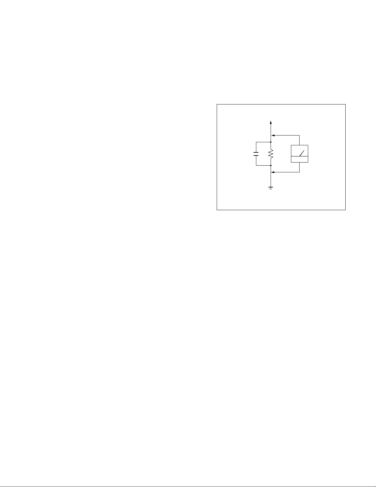
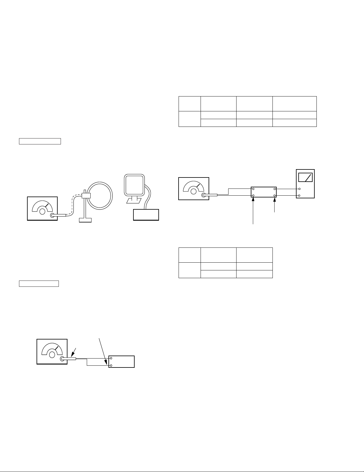
SAFETY CHECK-OUT
Earth Ground
Fig. A. Using an AC voltmeter to check AC leakage.
AC
Voltmeter
(0.75V)
0.15 F
µ
1.5k
Ω
To Exposed Metal
Parts on Set
After correcting the original service problem, perform the following
safety check before releasing the set to the customer :
Check the antenna terminals, metal trim, "metallized" knobs, screws,
and all other exposed metal parts for AC leakage. Check leakage as
described below.
LEAKAGE TEST
The AC leakage from any exposed metal part to earth ground and
from all exposed metal parts to any exposed metal part having a return to chassis, must not exceed 0.5mA (500 microampers).
Leakage current can be measured by any one of three methods.
1. A commercial leakage tester, such as the Simpson 229 or RCA
WT-540A. Follow the manufacturers’ instructions to use these
instruments.
2. A battery-operated AC milliammeter. The Data Precision 245
digital multimeter is suitable for this job.
3. Measuring the voltage drop across a resistor by means of a VOM
or battery-operated A C voltmeter . The “limit” indication is 0.75V,
so analog meters must have an accurate low-voltage scale. The
Simpson 250 and Sanwa SH-63Trd are examples of a passi ve V OM
that is suitable. Nearly all battery operated digital multimeters that
have a 2V AC range are suitable. (See Fig. A)
– 3 –
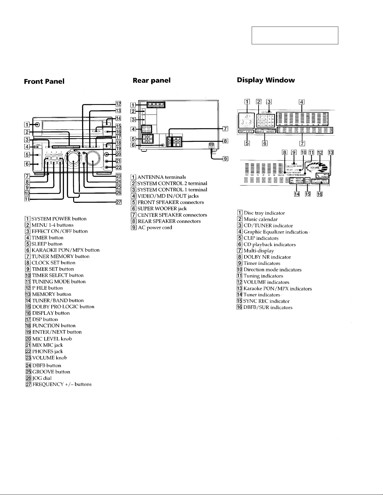
INDEX TO PARTS AND CONTROLS
SECTION 1
GENERAL
This section is extracted from
instruction manual.
– 4 –

SECTION 2
TEST MODE
DISPLAY / KEY TEST MODE
Press the ENTER/NEXT and FUNCTION buttons simultaneously.
Then press the MENU 1 button with the following 4 seconds to set the Test Mode.
1. The message “W3 NA (destination) ” appears on the screen and a 32 cycle square wa ve of the subcrystal oscillator is output from Pin 24
(AUB. OUT).
2. Press any key to rotate JOG and all FL indicators light up.
When you rotate JOG at this point, the display changes as follows.
N all FL indicators on Nn FL pattern 1 Nn FL pattern 2 n
The changes and all LED indicators light up.
3. Again press any key to set the key count check. The following display appears.
000
The numbers in order from left to right show ; the number of keys pressed, the JOG count (1 click per 4 counts), and the VOL count.
(1 cycle is a count of 96.)
4. Press the Power button to reset to the factory settings.
AMP TEST MODE
Press the ENTER/NEXT and FUNCTION buttons simultaneously.
Then press the MENU 2 button with the following 4 seconds to set the Test Mode.
1. The message “AMP TEST” appears on the screen. Press the MENU button to call up the Equalizer Curve for the Amp Test.
However when the function is set to the tuner, use the MENU button to call up each tuner preset from 1 through 5.
2. Press the Power button to reset to the factory settings.
MICROCOMPUTER COLD START
Press the ENTER/NEXT and FUNCTION buttons simultaneously.
Then press the MENU 3 button with the following 4 seconds to reset the microcomputer to the factory settings.
SUBCRYST AL TEST MODE
Press the ENTER/NEXT and FUNCTION buttons simultaneously.
Then press the MENU 4 button with the following 4 seconds.
The message “XT AL TEST ” appears on the screen and a 32 cycle square w ave of the subcrystal oscillator is output from Pin 24 (A UB.OUT).
In addition, a square wave of the same frequency as the subcrystal oscillator, is output from 4PIN (POWER. ON/OFF).
Press the Power button to reset to the factory settings.
– 5 –
SECTION 3
ELECTRICAL ADJUSTMENTS
Precautions in Repairing
Note. 1 : The adjustment should be performed in the publication.
(MW n FM n SW)
Note. 2 : As a front-end (FE1) is difficult to repair if faulty, replace
it with new one.
r
Abbreviation
AUS : Australian AR : Argentine
EA : Saudi Arabia HK : Hong Kong
SP : Singapore JE : Tourist
MY : Malaysia TH : Thailand
CND : Canadian
E2 : Tuner sections SW BAND do not exist.
E3 : Tuner sections SW BAND exist.
MW SECTION
MW Tuned Indication Lighting Level
Setting :
Band : MW
loop antenna A
AM RF signal
generator
loop antenna B
set
SW Control Voltage Adjustment
(Frequency Coverge Adjustment)
(E3, EA, MY, SP, HK, JE model)
Setting :
Band : SW
Procedure :
1. Connect digital Voltmeter to diode D1 center lead and ground.
2. Adjust for a following value reading on digital Voltmeter.
SW
Set frequency
5.95MHz T2 1.2Vdc
17.9MHz CV2 8.5Vdc
Adjustment
part
Reading on digital
voltmeter
SW T racking Adjustment
(E3, EA, MY, SP, HK, JE model)
Setting :
Band : SW
AM RF signal
generator
Modulation : 400Hz
30% modulation
set
SPEAKER terminal
VTVM
+
–
Carrier frequency : 999kHz (at 9kHz step)
1,050kHz (at 10kHz step)
Procedure :
1. Set loop antenna A so that the loop antenna B input lev el becomes
55dBµ/m (0.6mV/m)
2. Tune the set to 999kHz or 1,050kHz.
3. Adjust RV41 so that the TUNED indicatior goes on.
FM SECTION
FM Tuned Indication Lighting Level
Note : Always make the tuning level adjustment first.
(Since it affects the FM tuning level.)
Setting :
Band : FW
FM RF stereo signal
generator
75
Carrier frequency : 98MHz
Modulation : OFF
Output level : 0.018mV (25dB )
Procedure :
1. Tune the set to 98MHz.
2. Adjust RV42 so that the TUNED indicator goes on.
FM ANTENNA terminal
Ω
coaxial
µ
set
AM ANTENNA terminal
Procedure :
Adjust for maximum reading on VTVM.
Set frequency
SW
r
Repeat the procedures is each adjustment several times, and the
7MHz T1
17MHz CV1
Adjustment
part
frequency coverage and tracking adjustment should be finally done
by the trimmer capacitors.
Adjustment Location : TCB board
– 6 –
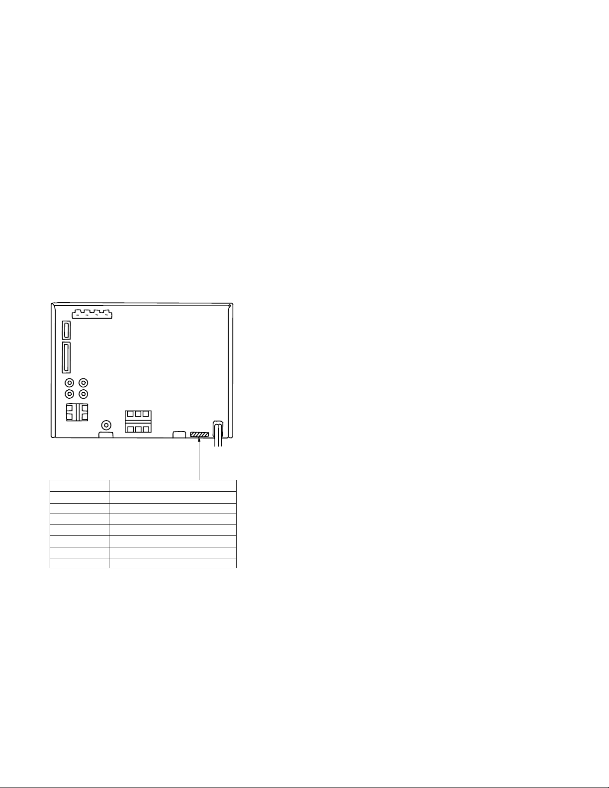
Adjustment Location
[TCB BOARD] – Component side –
RV41 : MW Tuned indication Lighting Level
CV1 : SW Tracking Adjustment
T1 : SW Tracking Adjustment
CV2 : SW Control Voltage Adjustment
T2 : SW Control Voltage Adjustment
RV42 : FW Tuned indication Lighting Level
D1
FE1
– 7 –

SECTION 4
EXPLANATION OF IC TERMINALS
IC501 ASD0205GF-015-3BA (SYSTEM CONTOROL)
Pin No. Pin name I/O Description
1 VDD – Power supply.
2 CLK OUT O Direct output for communications with HCD-W55.
3 RDY IN I/O Direct input / output for communications with HCD-W55.
4 POWER ON / OFF O L : Relay ON
5 MUTE O Mute output to transistor. L : Mute ON
6 PROLOGIC LATCH O Latch output to IC3001 (LA2785).
7 VOL. LATCH O Latch output to IC2002 (TC9210P).
8 427LAT O Latch output to IC105 (M62427FP).
9 LED LAT O Latch output to IC504 (M66313FP-200C).
10 RESET I Reset terminal.
11 X2 – Oscillator connection terminal. (5MHz)
12 X1 – Oscillator connection terminal. (5MHz)
13 IC – Ground connection.
14 XT2 – Oscillator connection terminal. (32MHz)
15 XT1 – Oscillator connection terminal. (32MHz)
16 VDD – Power supply.
17 BACK UP I AC Power supply OFF.
18 COM CLK O Transfer clock output serial data.
19 COM DATA O Serial data output.
20 ST DATA IN I Serial data input from IC 1.
21 ST CE O Chip enable output to IC 1.
22 STEREO I Stereo signal input.
23 TUNED I Tuned signal input.
24 AUB OUT O Audio bus output.
25 AVSS – Ground.
26 PROLOGIC. RY O Rear and center speaker relay ON/OFF control.
27 SUFFIX I Input for model select.
28 SPE I Spectrum analyzer signal input.
29 SPE I Spectrum analyzer signal input.
30 SPE I Spectrum analyzer signal input.
31 SPE I Spectrum analyzer signal input.
32 KYE 1 I Key data input (A/D converter).
33 KYE 2 I Key data input (A/D converter).
34 AVDD – Power supply for anlog.
35 AV REF – Reference voltage for A/D converter.
– 8 –
Pin No. Pin name I/O Description
36 VOL IN A I Volume encoder input.
37 JOG IN A I JOG dial encoder input.
38 RDS CLK I Not uset.
39 AUB IN I Audio bus output.
40 VSS – Ground.
41 RDS DATA I Not uset.
42 D 3 I/O System control data signal input / output.
43 D 2 I/O System control data signal input / output.
44 D 1 I/O System control data signal input / output.
45 D 0 I/O System control data signal input / output.
46 VDD – Power supply +5V.
47 SIRCS IN I SIRCS signal input.
48 VOL IN B I Volume encoder input.
49 JOG IN B I JOG dial encoder input.
50 ST FM O
BAND select output.
51 ST MUTE O
52 EMG OUT O Urgent signal standby output. “H” : standby
53 EMG IN I Urgent signal start input. “H” n “L” : start
57 – 78 P 32 – P 8 O Segment output to FL501.
79 VG – Power supply for fluorescent indicator tube.
80 – 86 P 7 – P 1 O Segment output to FL501.
87 – 100 14 G – 1 G O Grid output for FL501.
%º pin H L H
%¡ pin L L H
FM Receiving AM Receiving MUTE
– 9 –

– 10 –

– 11 –
 Loading...