

Page 1
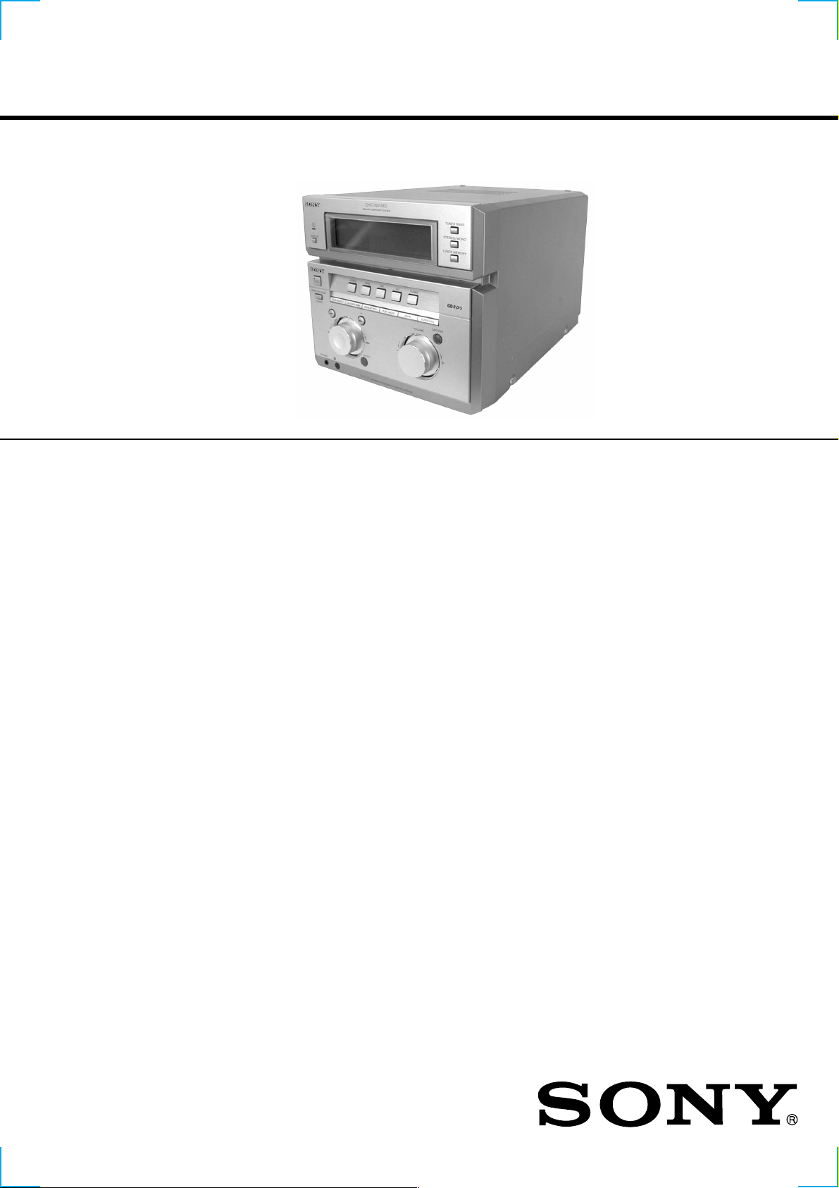
STR-NX5MD
g
SERVICE MANUAL
STR-NX5MD is the
Tuner and Amplifier
Section in DHC-NX5MD.
SPECIFICATIONS
Amplifier section
European model
DIN power output (rated) 80 + 80 watts
Continuous RMS power output (reference)
Music power output (reference)
Other models
DIN power output (rated) 90 + 90 watts
Continuous RMS power output (reference)
Inputs
VIDEO IN: voltage 250 mV
(phono jacks) impedance 47 kilohms
TAPE IN: voltage 250 mV
(phono jacks) impedance 47 kilohms
Outputs
TAPE OUT: voltage 250 mV
(phono jacks) impedance 1 kilohms
PHONES: accepts headphones of 8 ohms or
(stereo mini jack) more
FRONT SPEAKER: accepts impedance of 6 to 16 ohms
REAR SPEAKER: accepts impedance of 16 ohms
SUPER WOOFER: volta
(6 ohms at 1 kHz, DIN)
100 + 100 watts
(6 ohms at 1 kHz, 10% THD)
160 + 160 watts
(6 ohms at 1 kHz, 10% THD)
(6 ohms at 1 kHz, DIN)
110 + 110 watts
(6 ohms at 1 kHz, 10% THD)
e 1 V, impedance 1 kilohms
Tuner section
FM stereo, FM/AM superheterodyne tuner
FM tuner section
Tuning range
Tourist model: 76.0 – 108.0 MHz
Other models: 87.5 – 108.0 MHz
Aerial FM lead aerial
Aerial terminals 75 ohm unbalanced
Intermediate frequency 10.7 MHz
AM tuner section
Tuning range
European models: 531 – 1,602 kHz
(with the interval set at 9 kHz)
Other models: 531 – 1,602 kHz
(with the interval set at 9 kHz)
530 – 1,710 kHz
(with the interval set at 10 kHz)
Aerial AM loop aerial
Aerial terminals External aerial terminal
Intermediate frequency 450 kHz
AEP Model
UK Model
E Model
General
Power requirements
European models: 230 V AC, 50/60 Hz
Other models: 120 V, 220 V or 230 – 240 V AC,
Power consumption
European models: 190 watts
Other models: 220 watts
Dimensions (w/h/d) Approx. 225 × 202 × 356 mm
Mass
European models: Approx. 7.8 kg
Other models: Approx. 7.6 kg
Supplied accessories: AM loop aerial (1)
Design and specifications are subject to change
without notice.
50/60 Hz Adjustable with voltage
selector
Remote Commander (1)
Batteries (2)
FM lead aerial (1)
Speaker cords (2)
Front speaker pads (8)
TUNER/AMPLIFIER
1
Page 2
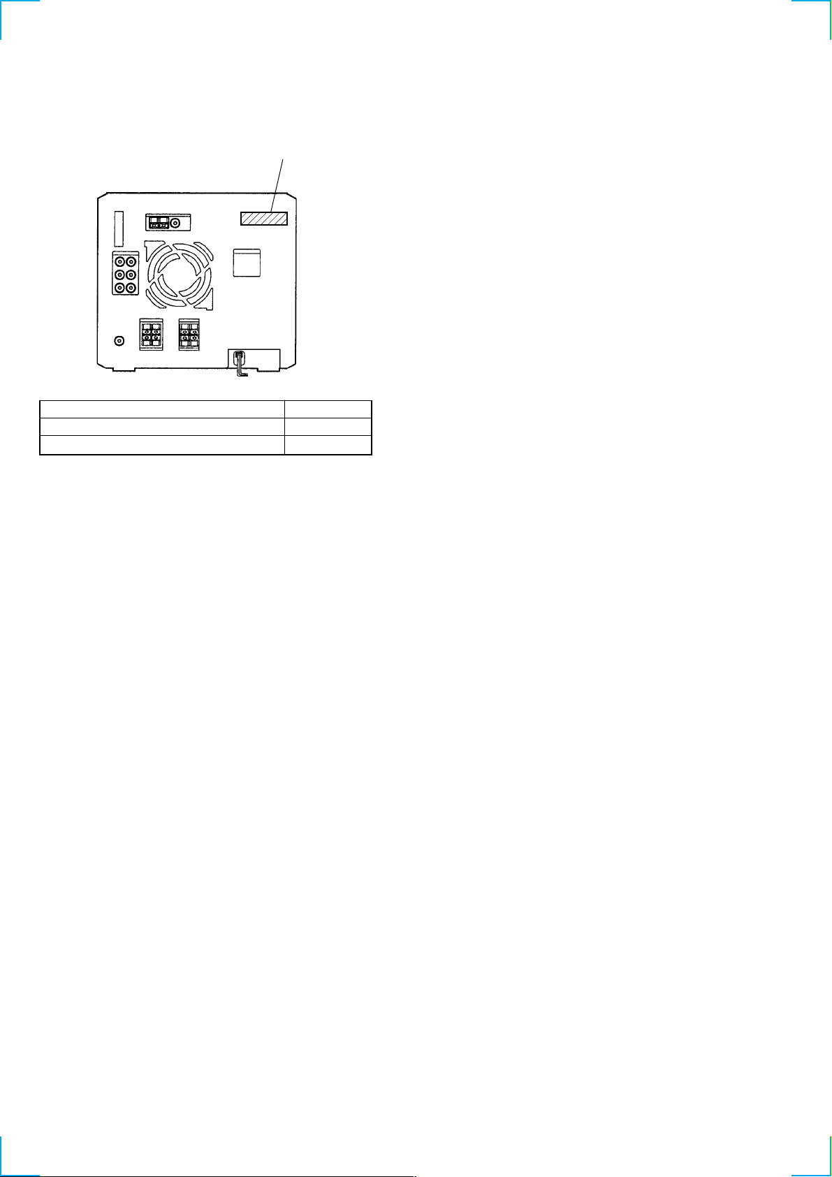
• MODEL IDENTIFICATION
– Rear Panel –
PART No.
MODEL PART No.
AEP, UK, G, AED and CIS models 4-221-391-8[]
Malaysia and Singapore models 4-221-391-9[]
• Abbreviation
G : German model
AED : North European model
TABLE OF CONTENTS
1. GENERAL .......................................................................... 3
2. DISASSEMBLY
2-1. Case ....................................................................................... 5
2-2. Front Panel Assy ................................................................... 5
2-3. Back Panel Assy .................................................................... 6
2-4. Main Board ........................................................................... 6
3. TEST MODE ........................................................................ 7
4. DIAGRAMS
4-1. Notes for Printed Wiring Boards and Schematic Diagrams.. 9
4-2. Schematic Diagram – Main Board (1/3) – .......................... 10
4-3. Schematic Diagram – Main Board (2/3) – .......................... 11
4-4. Schematic Diagram – Main Board (3/3) – .......................... 12
4-5. Printed Wiring Board – Main Board – ................................ 13
4-6. Printed Wiring Board – PA Board – .................................... 14
4-7. Schematic Diagram – PA Board – ...................................... 15
4-8. Printed Wiring Board – Panel Section – ............................. 16
4-9. Schematic Diagram – Panel Section – ................................ 17
4-10. Printed Wiring Board – Transformer Section – ................. 18
4-11. Schematic Diagram – Transformer Section – ................... 19
4-12. IC Pin Function Description ............................................. 20
5. EXPLODED VIEW
5-1. General Section ................................................................... 22
5-2. Front Panel Section ............................................................. 23
5-3. Chassis Section ................................................................... 24
6. ELECTRICAL PARTS LIST ........................................ 25
SAFETY-RELATED COMPONENT WARNING!!
COMPONENTS IDENTIFIED BY MARK 0 OR DOTTED
LINE WITH MARK 0 ON THE SCHEMATIC DIAGRAMS
AND IN THE PARTS LIST ARE CRITICAL TO SAFE
OPERATION. REPLACE THESE COMPONENTS WITH
SONY PARTS WHOSE PART NUMBERS APPEAR AS
SHOWN IN THIS MANUAL OR IN SUPPLEMENTS PUBLISHED BY SONY.
2
Page 3
• LOCATION OF CONTROLS
1 2 3
5 6 7 8 9 0
– Front Panel –
4
3
2
1
wh
wg
wf
SECTION 1
GENERAL
1 ?/1 (Power) button and indicator
2 CD/TUNER NAME button
qa
qs
qd
qf
qg
qh
qkqlwswd w;wa
qj
3 DISPLAY button
4 TIMER indicator
(AEP, UK, German, AED and CIS models)
5 VIDEO button
6 TAPE button
7 MD button
8 CD button
9 TUNER button
q; Display window
qa TUNER BAND button
qs STEREO/MONO button
qd TUNER MEMORY button
qf DBFB button
qg SURROUND button
qh GROOVE button and indicator
qj VOLUME knob
qk PLAY MODE button
ql REPEAT/PTY button
w; + M button
wa ENTER button and indicator
ws Remote sensor
wd PHONES jack
wf Jog dial
wg – m button
wh POWER SAVE/DEMO (STANDBY) button
wj FILE SELECT button
– Rear Panel –
0
9
8
6 57
Photo: AEP model
4
1 SYSTEM CONTROL terminals
2 AM ANTENNA terminals
3 FM ANTENNA terminal
4 VOLTAGE SELECTOR switch
(Malaysia and Singapore models)
5 REAR SPEAKER terminals
6 CENTER SPEAKER terminals
7 SUPER WOOFER OUT jack
8 MD OUT jacks
9 MD IN jacks
q; VIDEO (AUDIO) jacks
• Abbreviation
AED : North European model
3
Page 4
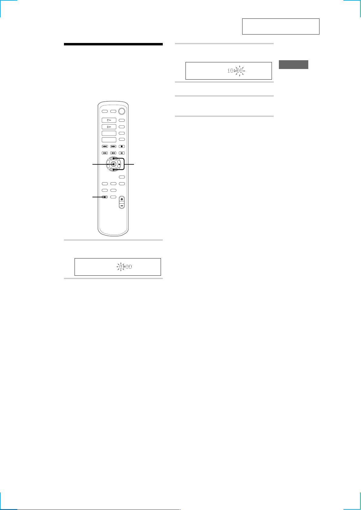
Step 2: Setting the time
You must set the time beforehand to use the timer
functions.
The clock is on a 24-hour system for the European
model, and a 12-hour system for other models.
The 24-hour system is used for illustration
purposes.
3,5 2,4
1
This section is extracted from
instruction manual.
3
Press ENTER.
The minute indication flashes.
4
Press V or v to set the minute.
5
Press ENTER.
The clock starts.
Tips
• If you’ve made a mistake, start over from step 1.
• Setting the time deactivates the demo mode.
If you want to display the demo mode, press
DISPLAY (European model) or DEMO
(STANDBY) (other models) when the power is off.
To change the time
The previous explanation shows you how to set
the time while the power is off. To change the
time while the power is on, do the following:
1 Press CLOCK/TIMER SET.
2 Press V or v to select the SET CLOCK.
3 Press ENTER.
4 Perform steps 2 through 5 above.
Note
The clock settings are cancelled when you disconnect
the mains lead or if a power failure occurs.
Getting Started
1
Press CLOCK/TIMER SET.
The hour indication flashes.
2
Press V or v to set the hour.
7
4
Page 5
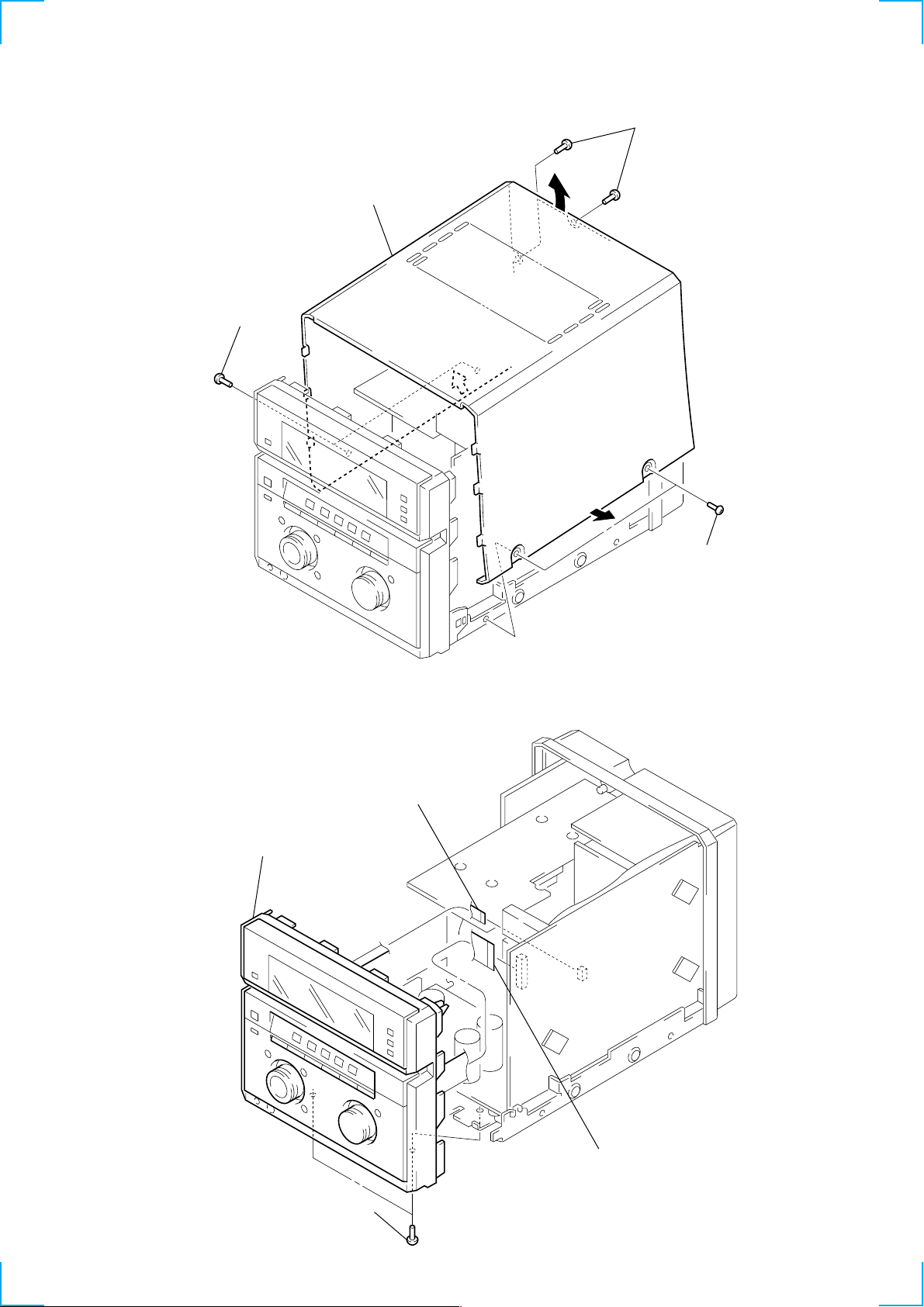
SECTION 2
DISASSEMBLY
Note: Follow the disassembly procedure in the numerical order given.
2-1. CASE
3 case
1 two screws
(case 3 TP2)
2 two screws
(BVTP3 × 10)
1 two screws
(case 3 TP2)
2-2. FRONT PANEL ASSY
4 front panel assy
1 flat cable (7 core)
(CN132)
2 flat cable (25 core)
(CN131)
3 two screws
(BVTT3 × 6)
5
Page 6
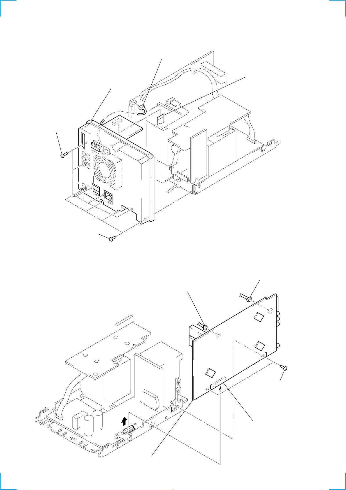
2-3. BACK PANEL ASSY
)
3 six screws
(BVTP3 × 10)
4 back panel assy
2 connector
(CN173)
1 flat cable (13 core)
(CN1)
2-4. MAIN BOARD
3 four screws
(BVTP3 × 10)
2 connector (CN111)
1 connector
(CN181)
3 two screws
(BVTP3 × 10)
4 connector (CN152
5 main board
6
Page 7

SECTION 3
TEST MODE
[CD Delivery Mode]
• This mode moves the optical pick-up to the position durable to
vibration. Use this mode when returning the set to the customer
after repair.
Procedure:
1. Press the ?/1 button to turn the power ON.
2. Press the [ENTER] and ?/1 buttons simultaneously.
3. A message “LOCK” is displayed on the liquid crystal display,
and the CD delivery mode is set.
[Change-over the MW Tuning Interval]
• The MW tuning interval can be changed over 9 kHz or 10 kHz.
Procedure:
1. Press the ?/1 button to turn the power ON.
2. Press the [TUNER] button to select the function “TUNER”,
and press the [TUNER BAND] button to select the BAND “MW”.
3. Press the ?/1 button to turn the power OFF.
4. Press the [TUNER MEMORY] and ?/1 buttons simultaneously,
and the display on the liquid crystal display changes to “MW
9 k STEP” or “MW 10 k STEP”, and thus the tuning interval
is changed over.
[MC Cold Reset]
• The cold reset clears all data including preset data stored in the
RAM to initial conditions. Execute this mode when returning
the set to the customer.
Procedure:
1. Turn the power ON or set to the DEMO mode.
2. Press the [GROOVE] and ?/1 buttons simultaneously.
3. The set is reset, and displays “COLD RESET”, then becomes
DEMO mode.
[Amplifier Test Mode]
Procedure:
1. Press the
2. Press three buttons of [ENTER] , [DISPLAY] , and
?/1 button to turn the power ON.
[TUNER BAND] simultaneously.
3. “ALC OFF” is displayed, then the function which was set be-
fore the test mode became active is displayed.
[LED and Liquid Crystal Display All Lit, Software Version Display, Key Check, VACS Level Display Mode]
Procedure:
1. Press the ?/1 button to turn the power ON.
2. Press three buttons of [ENTER] , [DISPLAY] , and
[STEREO/MONO] simultaneously.
3. LEDs and liquid crystal display are all turned on.
Rotating the JOG dial changes over the check patterns of liquid crystal display.
4. Successively, the following three modes can be activated.
(1) Press the [VIDEO] button, and the software version is displayed
on the liquid crystal display.
(2) Press the [MD] button, and the key check mode is activated.
In the key check mode, the liquid crystal display displays “K
0 J0 V0”. Each time a button is pressed, “K” value increases.
However, once a button is pressed, it is no longer taken into
account.
“J” value increases like 1, 2, 3 ... if turn the JOG dial clockwise, or it decreases like 0, 9, 8 ... if turn the JOG dial counterclockwise.
“V” value increases like 1, 2, 3 ... if turn the [VOLUME] dial
clockwise, or it decreases like 0, 9, 8 ... if turn the JOG dial
counterclockwise.
(3) Press the [TAPE] button, and the VACS level is displayed on
the liquid crystal display.
5. To release from these mode, press three buttons in the same
manner as step 2, or remove the power cord.
[MC Hot Reset]
• This mode resets the set with the preset data kept stored in the
memory. The hot reset mode functions same as if the power
cord is plugged in and out.
Procedure:
1. Turn the power ON or set to the DEMO mode.
2. Press three buttons of
[ENTER] , [DISPLAY] , and
[TUNER MEMORY] simultaneously.
3. The set is reset, and becomes standby state.
[Change-over of VACS ON/OFF]
Procedure:
1. Press the ?/1 button to turn the power ON.
2. Press three buttons of [ENTER] , [DISPLAY] , and [GROOVE]
simultaneously, and the display on the liquid crystal display
changes to “VACS ON” or “VACS OFF”, and thus the VACS
ON/OFF is changed over.
[VIDEO input, Record and CD play in CD function]
Procedure:
1. Press the ?/1 button to turn the power ON.
2. Press three buttons of [ENTER] , [DISPLAY] , and
- m simultaneously.
3. “DVD 5.1CH” is displayed on liquid crystal display, and at
the same time, CD is played and the deck B is placed in the
record status.
[CD Service Mode]
• This mode can run the CD sled motor optionally. Use this mode,
for instance, when cleaning the optical pick-up.
Procedure:
1. Press the ?/1 button to turn the power ON.
2. Press the
3. Press three buttons of [ENTER] , [POWER SAVE/DEMO
(
STANDBY) , and [STEREO/MONO] simultaneously.
4. Set to the Sled Servo mode.
5. With the CD in stop status, turn the JOG dial clockwise to
move the optical pick-up to outside track, or turn it counterclockwise to inside track.
6. To release from this mode, perform as follows.
1) Move the optical pick-up to the most inside track.
2) Remove the power cord.
Notes: • Always move the optical pick-up to most inside track when
[CD] button to select the function “CD”.
releasing from this mode. Otherwise, a disc will not be unloaded.
• Do not run the sled motor excessively, otherwise the gear can
be chipped.
7
Page 8
[Aging Mode]
This mode can be used for operation check of CD section and tape
deck section.
CD section and tape deck section work in parallel.
• If an error occurred:
The aging operation stops only an error occurred sections and
display then status.
• If no error occurs:
The aging operation continues repeatedly.
Procedure:
1. Set disc in DISC5 tray.
2. Load the tapes into the decks A and B respectively.
3. Press the [PLAY MODE] button to set the “ALL DISCS” mode,
and press the [REPEAT/PTY] button to “REPEAT” off.
4. Press the [CD] button to select the function “CD”.
5. Press three buttons of [ENTER] , [POWER SAVE/DEMO
(
STANDBY) , and [TUNER BAND] simultaneously.
6. The aging mode is activated, if the indicator of disc tray num-
ber on the liquid crystal display is blinking.
7. To release from the aging mode, press the ?/1 button to turn
the power OFF and operate the cold reset. (Refer to the “MC
Cold Reset”)
• Display at an error occurred
1) Display of the error count
(1) Press three buttons of [ENTER] , [POWER SAVE/DEMO
(
STANDBY)
, and [GROOVE] simultaneously.
(2) Display of the error count following as below.
Display
EMC**EDC
Notes:
EMC**: The number of mechanical error.
EDC**: The number of no disc error after chucking the disc.
**
2) Display of mechanical error
Display
E**M##$$&&
1. Display at the Aging Mode
• Display operating state of CD section and tape deck section alternately.
• If an error occurred, stop display which that section.
2. CD Section
• Display at the aging mode is the same as the normal operation.
• The sequence during the aging mode is following as below.
Aging mode sequence (CD section) :
Open the disc1 tray
Disc5 chucking
Disc5 TOC read
Disc5 play track1 for 2 seconds
Disc5 play last track for 2 seconds
Notes:
: The number of mechanical error.(“00” is latest one)
**
(Press the [PLAY MODE] button to changes next error display)
## : Not used.
$$ : Loading error. (Second figure is not used)
D : The error in the midst of close at the except mechanical trouble.
E : The error in the midst of open at the except mechanical trouble.
C : The error in the midst of chuck up at the except mechanical
trouble.
F : The error in the midst of EX-open at the except mechanical
trouble.
&&: Loading error. (Second figure in not used)
1:The error in the midst of chuck up.
2:The error in the midst of chuck down.
3:Time up of EX-open
4:Time up of EX-close.
3) Display of no disc error
Display
E**D##$$&&
Notes:
: The number of mechanical error.(“00” is latest one)
**
(Press the [REPEAT] button to changes next error display)
##:
01:Focus error
02:GFS error
03:Set up error
$$:
00:No disc error when does not chucking retry.
02:No disc error when chucking retry to completion.
&&: The state when judged no disc error. (Second figure is not used)
1:Stop
2:Set up
3:TOC read
4:Access
5:Play
6:Pause
7:Manual search (Play)
8:Manual search (Pause)
8
Page 9
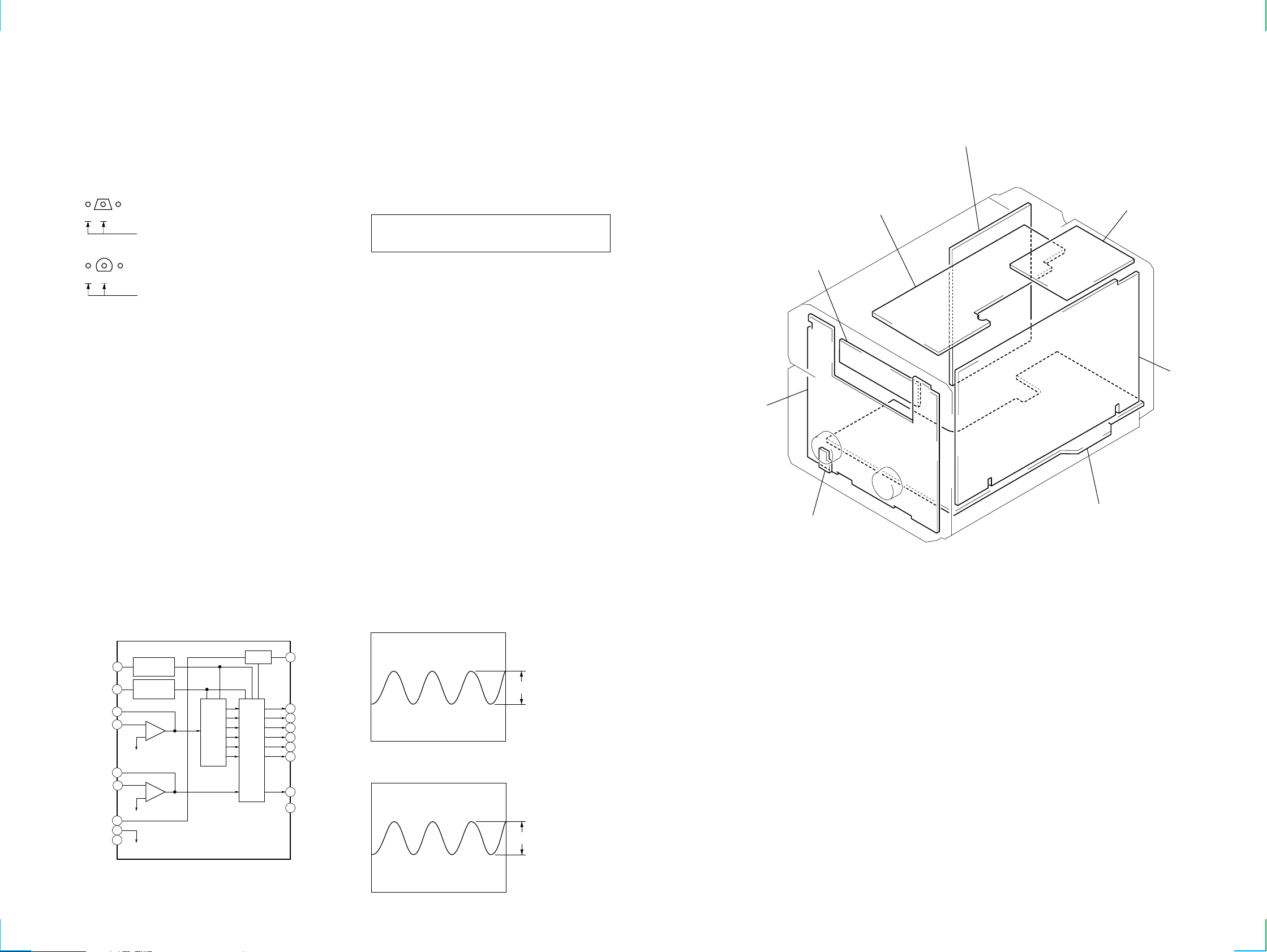
SECTION 4
SUB TRANS board
(AEP, UK, G, AED, CIS)
TRANS board
BACK LIGHT board
PANEL board
R board
PA board
MAIN board
TUNER pack
DIAGRAMS
4-1. NOTE FOR PRINTED WIRING BOARDS AND SCHEMATIC DIAGRAMS
Note on Printed Wiring Board:
• X : parts extracted from the component side.
• Y : parts extracted from the conductor side.
• x : parts mounted on the conductor side.
• b : Pattern from the side which enables seeing.
(The other layers' patterns are not indicated)
• Indication of transistor.
Q
B
CE
These are omitted.
Q
B
CE
These are omitted.
Note on Schematic Diagram:
• All capacitors are in µF unless otherwise noted. pF: µµF
50 WV or less are not indicated except for electrolytics
and tantalums.
• All resistors are in Ω and 1/
specified.
f
•
: internal component.
• 2 : nonflammable resistor.
• 5 : fusible resistor.
• C : panel designation.
Note: The components identified by mark 0 or dotted line
with mark 0 are critical for safety.
Replace only with part number specified.
• U : B+ Line.
• V : B– Line.
• Voltages and waveforms are dc with respect to ground
under no-signal (detuned) conditions.
no mark : TUNER (FM)
• Voltages are taken with a VOM (Input impedance 10 MΩ).
Voltage variations may be noted due to normal production tolerances.
• Waveforms are taken with a oscilloscope.
Voltage variations may be noted due to normal production tolerances.
• Circled numbers refer to waveforms.
• Signal path.
F : FM
E : MD PLAY
J : CD PLAY
j : MD REC
• Abbreviation
MY : Malaysia model
SP : Singapore model
G : German model
AED : North European model
4
W or less unless otherwise
• Circuit Boards Location
• IC Block Diagram
– MAIN Board –
1
2
3
4
5
6
7
8
9
REFERENCE
REFERENCE
IC401 BA3830F
R02
R01
LINE NF
LINE IN
REC NF
REC IN
RESET C
BIAS C
GND
CURRENT
CURRENT
–
+
–
+
BAND
PASS
FILTER
RESET
DET
18
17
16
15
14
13
12
11
10
RESET
F01
F02
F03
F04
F05
F06
REC LEVEL
VCC
• Waveforms
– MAIN Board –
1 IC501 qa (XCOUT)
32.768 kHz
2 IC501 qd (XOUT)
3 Vp-p
2.8 Vp-p
16.025 MHz
99
Page 10
STR-NX5MD
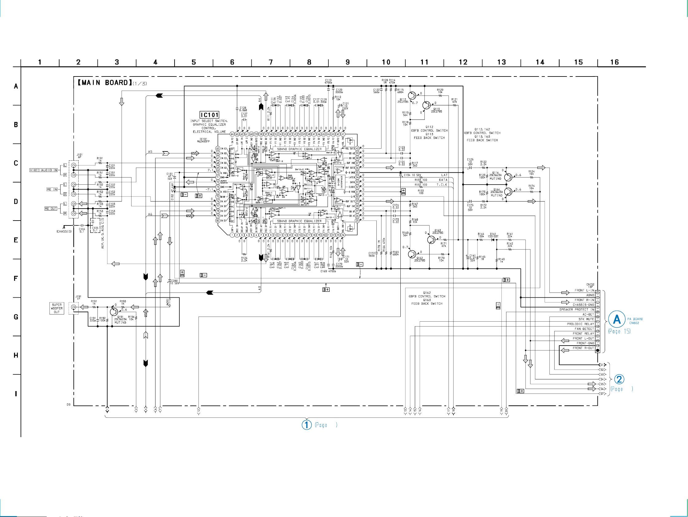
4-2. SCHEMATIC DIAGRAM – MAIN Board (1/3) – • See page 13 for Printed Wiring Board.
11
10 10
12
Page 11

4-3. SCHEMATIC DIAGRAM – MAIN Board (2/3) – • See page 9 for Waveforms. • See page 13 for Printed Wiring Board.
10
STR-NX5MD
PIN FUNCTION
12
11 11
Page 12

STR-NX5MD
4-4. SCHEMATIC DIAGRAM – MAIN Board (3/3) – • See page 9 for IC Block Diagram.
10
• Semiconductor Location
Ref. No. LocationRef. No. Location
D141 A-8
D501 B-2
D502 D-1
D503 D-1
D504 E-1
D505 E-1
D506 E-1
D507 F-1
D508 E-2
D510 C-1
D901 B-5
D902 B-5
D903 B-5
D904 B-4
D905 A-6
D906 A-6
D914 A-3
D915 B-3
D920 B-4
D921 B-3
D925 B-4
D931 A-4
D932 A-4
IC101 B-9
IC401 E-5
IC501 E-3
IC502 E-1
IC901 A-2
IC921 C-2
Q112 A-8
Q113 A-8
Q114 G-6
Q162 A-9
Q163 A-9
Q164 G-6
Q191 G-11
Q411 D-5
Q421 C-3
Q431 E-6
Q432 D-6
Q461 D-5
Q501 F-1
Q502 F-1
Q503 F-1
Q901 A-6
Q902 A-6
Q903 A-6
Q904 A-3
Q905 A-3
Q906 B-3
Q907 B-4
Q921 B-3
Q926 B-3
Q927 B-3
Q951 B-6
Q952 B-6
Q953 B-6
11
12 12
Page 13

4-5. PRINTED WIRING BOARD – MAIN Board – • See page 9 for Circuit Boards Location.
(Page 18)
STR-NX5MD
(Page 18)
(Page 16)
(Page 16)
(Page 18)
(Page 14)
There are a few cases that the part isn’t mounted in
model is printed on diagram.
13 13
Page 14

STR-NX5MD
4-6. PRINTED WIRING BOARD – PA Board – • See page 9 for Circuit Boards Location.
MAIN
BOARD
CN152
(Page 13)
(AEP, UK, AED, CIS)
(AEP, UK,
AED, CIS)
(MY, SP)
(MY, SP)
TRANS
BOARD
CN952
(Page 18)
14 14
• Semiconductor Location
Ref. No. LocationRef. No. Location
D802 B-5
D821 E-4
D831 C-6
D852 C-5
D871 B-10
D881 E-2
D883 A-11
D884 C-11
D885 F-10
There are a few cases that the part isn’t mounted in
model is printed on diagram.
IC801 C-8
Q801 B-5
Q821 D-7
Q822 D-7
Q823 C-7
Q824 C-7
Q825 H-4
Q826 H-4
Ref. No. Location
Q827 H-4
Q828 G-4
Q829 G-4
Q830 G-4
Q831 C-7
Q851 C-5
Q881 B-10
Q882 B-9
Page 15

4-7. SCHEMATIC DIAGRAM – PA Board –
STR-NX5MD
15 15
Page 16

STR-NX5MD
4-8. PRINTED WIRING BOARDS – PANEL Section – • See page 9 for Circuit Boards Location.
• Semiconductor
Location
Ref. No. Location
D631 E-2
D636 G-5
D637 A-8
D638 D-8
D643 C-6
D644 C-7
D645 C-4
D646 C-5
D647 C-2
D648 C-3
(Page 13)
Q631 E-1
Q636 F-5
Q637 B-7
Q638 D-8
Q641 D-7
Q642 D-7
Q643 D-7
16 16
(Page 13)
There are a few cases that the part isn’t mounted in
model is printed on diagram.
Page 17

4-9. SCHEMATIC DIAGRAM – PANEL Section –
STR-NX5MD
17 17
Page 18

STR-NX5MD
4-10. PRINTED WIRING BOARDS – TRANSFORMER Section – • See page 9 for Circuit Boards Location.
(AEP, UK, G,
AED, CIS)
1
(AEP, UK, G,
AED, CIS)
(MY, SP)
(MY, SP)
JW953
(MY, SP)
CN952
MAIN
BOARD
(Page 13)
(Page 13)
(Page 14)
10
CN111
MAIN
BOARD
CN181
PA
BOARD
CN808
09
(Page 13)
18 18
There are a few cases that the part isn’t mounted in
model is printed on diagram.
Page 19

4-11. SCHEMATIC DIAGRAM – TRANSFORMER Section –
STR-NX5MD
19 19
Page 20

4-12. IC PIN FUNCTION DESCRIPTION
• MAIN BOARD IC501 M30622MAA-A39FP (SYSTEM CONTROLLER )
Pin No. Pin Name I/O Descriptions
1 L+R I
2 BPF SL I
3 F RELAY O Speaker protect relay drive signal output for the front side speaker “H”: relay on
4 R RELAY O Speaker protect relay drive signal output for the rear side speaker “H”: relay on
5 SIRCS I Remote control signal input from the remote control receiver (IC601)
6 LINE MUTE O Line muting on/off control signal output terminal “L”: muting on
7 DBFB O
8 BYTE I External data bus line byte selection signal input terminal Fixed at “L” in this set
9 CNVSS — Ground terminal
10 XCIN I Sub system clock input terminal (32.768 kHz)
11 XCOUT O Sub system clock output terminal (32.768 kHz)
12 RESET I
13 XOUT O Main system clock output terminal (16 MHz)
14 VSS — Ground terminal
15 XIN I Main system clock input terminal (16 MHz)
16 VCC — Power supply terminal (+5V)
17 NMI I Non-maskable interrupt input terminal Fixed at “H” in this set
18 WAKE UP O Wakeup control signal output to the CPU on the HMC-NX5MD “H” active
19 PHONES MUTE O Muting on/off control signal output terminal “L”: muting on Not used (open)
20 RDS INT I
21 RDS DATA I
22 AC CUT I AC off detection signal input from the reset signal generator (IC502) “L”: AC cut checked
23 PL CLK O Not used (open)
24 PL DATA O Not used (open)
25 PL LAT O Not used (open)
26 STK POWER O Power amplifier on/off selection signal output terminal “L”: standby mode, “H”: on
27 SPEAKER PROTECT I
28 SOFT-TEST O Output terminal for the software test Not used (open)
29 IIC CLK I/O
30 IIC DATA I/O Communication data bus with the CPU on the HMC-NX5MD
31 TXD1 O Not used (open)
32 RXD1 I Not used (fixed at “L”)
33 CLK1 I Not used (fixed at “L”)
34 RTS1 O Not used (open)
35 LCD DAT A O Serial data output to the liquid crystal display unit (LCD601)
36 RXD0 I Not used (fixed at “L”)
37 LCD CLK O Serial data transfer clock signal output to the liquid crystal display unit (LCD601)
38 493 LT O Serial data latch pulse output to the M62493FP (IC101)
39 CLOCK OUT O Output terminal for the clock signal check Not used (open)
40 VC L+R/L–R O Virtual cinema L+R/L–R selection signal output terminal Not used (open)
Spectrum analyzer drive signal input from the spectrum analyzer band-pass filter (IC401)
(for VACS, non-stop signal)
Spectrum analyzer drive (super low frequency) signal input from the spectrum analyzer
band-pass filter (IC401) (for 40 Hz)
DBFB normal/high selection signal output to the M62493FP (IC101)
“L”: DBFB high, “H”: DBFB low/off
System reset signal input from the reset signal generator (IC502) “L”: reset
For several hundreds msec. after the power supply rises, “L” is input, then it changes to “H”
RDS serial data transfer clock signal input from the tuner pack
(Used for the AEP, UK, G*, AED* and CIS models only)
RDS serial data input from the tuner pack
(Used for the AEP, UK, G*, AED* and CIS models only)
Protect on/off detection signal input from the speaker protect circuit
“L”: protect on, “H”: protect off
Communication data reading clock signal input or transfer clock signal output with the CPU
on the HMC-NX5MD
Pin No. Pin Name I/O
41 XHOLD I Not used (fixed at “L”)
42 LCD SW O
43 STBY RELAY O
44 BASS FREQ O
45 OPT SEL O Not used (open)
46 XWR I Not used (fixed at “H”)
47 493 DATA O Serial data output to the M62493FP (IC101)
48 493 CLK O Serial data transfer clock signal output to the M62493FP (IC101)
49 ST MUTE O Tuner muting control signal output to the tuner pack “H”: muting on
50 STEREO I FM stereo detection signal input from the tuner pack “L”: stereo
51 TUNED I Tuning detection signal input from the tuner pack “L”: tuned
52 ST CE O PLL chip enable signal output to the tuner pack
53 ST DOUT O PLL serial data output to the tuner pack
54 ST DIN I PLL serial data input from the tuner pack
55 ST CLK O PLL serial data transfer clock signal output to the tuner pack
56 VC BYPASS O Virtual cinema bypass control signal output terminal Not used (open)
57 PHONES DETECT I
58 LCD LAT O Serial data latch pulse output to the liquid crystal display unit (LCD601)
59 LCD A0 O Address signal output to the liquid crystal display unit (LCD601)
60 LCD RESET O Reset signal output to the liquid crystal display unit (LCD601) “L”: reset
61 NC O Not used (open)
62 VCC — Power supply terminal (+5V)
63 NC O Not used (open)
64 VSS — Ground terminal
65 to 67 NC O Not used (open)
68 TUNER MUTE O TUNER 5V ON/OFF SW
69 JOG B I Jog dial pulse input from the rotary encoder (S652 JOG) (B phase input)
70 JOG A I Jog dial pulse input from the rotary encoder (S652 JOG) (A phase input)
71 VOL B I Jog dial pulse input from the rotary encoder (S651 VOLUME) (B phase input)
72 VOL A I Jog dial pulse input from the rotary encoder (S651 VOLUME) (A phase input)
73 to 75 NC O Not used (open)
76 HMC POWER O HMC POWER detection
77, 78 NC O Not used (open)
79 LED FUNCTION O LED drive signal output of the key illumination indicator (D643 to D648) “H”: LED on
80 LED POWER O LED drive signal output of the I/1 indicator (D638) “H”: LED on
81 LED TIMER O
82 LED LCD O
83 LED ENTER O LED drive signal output of the ENTER indicator (D636) “H”: LED on
84 LED JOG O LED drive signal output terminal Not used (open)
85 LED CINEMA O LED drive signal output terminal Not used (open)
86 LED DOLBY O
Liquid crystal display on/off selection signal output terminal “L”: on, “H”: off
Not used (open)
Main power on/off control signal output terminal “L”: standby mode, “H”: power on
(Used for the AEP, UK, G*, AED* and CIS models only)
Sync bass frequency normal/high selection signal output to the M62493FP (IC101)
“L”: sync bass off (normal), “H”: sync bass high Not used (open)
Connection detect signal input of the headphone jack (J701)
“L”: no connected, “H”: headphone connected
LED drive signal output of the TIMER indicator (D637) “H”: LED on
(Used for the AEP, UK, G*, AED* and CIS models only)
LED drive signal output of the liquid crystal display back light indicator (D639 to D642)
“H”: LED on
LED drive signal output of the PRO LOGIC indicator (D633) “H”: LED on
Not used (open)
Descriptions
20 20
Page 21

Pin No. Pin Name I/O
87 LED 5.1CH O
88 LED GROOVE O LED drive signal output of the GROOVE indicator (D631) “H”: LED on
89 BPF 1 I
90 BPF 2 I
91 BPF 3 I
92 BPF 4 I
93 KEY1 I
94 KEY0 I
95 MODEL-IN I Destination setting terminal
96 AVSS — Ground terminal (for A/D conversion)
97 SPEC-IN I Setting terminal for the version
98 VREF I Reference voltage (+5V) input terminal (for A/D conversion)
99 AVCC — Power supply terminal (+5V) (for A/D conversion)
100 POWER O Power on/off control signal output terminal “L”: standby mode, “H”: power on
LED drive signal output of the DVD 5.1CH indicator (D632) “H”: LED on
Not used (open)
Spectrum analyzer drive (low frequency) signal input from the spectrum analyzer band-pass
filter (IC401) (for 100 Hz)
Spectrum analyzer drive (low and middle frequency) signal input from the spectrum
analyzer band-pass filter (IC401) (for 400 Hz)
Spectrum analyzer drive (middle and high frequency) signal input from the spectrum
analyzer band-pass filter (IC401) (for 2 kHz)
Spectrum analyzer drive (high frequency) signal input from the spectrum analyzer band-
pass filter (IC401) (for 6 kHz)
Key input terminal (A/D input)
S615 to S617, S619 to S622 (TUNER BAND, STEREO/MONO, TUNER MEMORY,
GROOVE, + M, – m) keys input
Key input terminal (A/D input)
S601 to S614 (I/1, DISPLAY, POWER SAVE/DEMO (STANDBY), VIDEO/DVD, MD,
TAPE, CD, TUNER, DSB, DBFB, PLAY MODE, REPEAT, EDIT, FILE SELECT) keys
input
Descriptions
* Abbreviation
G : German model
AED : North European model
21
Page 22

SECTION 5
EXPLODED VIEWS
NOTE:
• -XX and -X mean standardized parts, so they
may have some difference from the original
one.
• Color Indication of Appearance Parts
Example:
KNOB, BALANCE (WHITE) . . . (RED)
↑↑
Parts Color Cabinet's Color
• Abbreviation
MY : Malaysia model
SP : Singapore model
G : German model
AED : North European model
5-1. GENERAL SECTION
2
• Items marked “*” are not stocked since they
are seldom required for routine service. Some
delay should be anticipated when ordering
these items.
• The mechanical parts with no reference number in the exploded views are not supplied.
• Hardware (# mark) list is given in the last of
the electrical parts list.
M401
#1
#1
6
#1
The components identified by
mark 0 or dotted line with mark
0 are critical for safety.
Replace only with part number
specified.
#1
#1
1
Front panel assy
#4
#1
#1
#1
4
1
3
5
Ref. No. Part No. Description Remark
1 3-363-099-11 SCREW(CASE 3 TP2)
2 4-221-365-11 CASE
3 X-4952-909-1 PANEL ASSY, BACK(MY,SP)
3 X-4952-910-1 PANEL ASSY, BACK(AEP,UK,G,AED,CIS)
4 1-751-688-11 WIRE(FLAT TYPE) (13 CORE)(MY,SP)
22
Ref. No. Part No. Description Remark
4 1-773-011-11 WIRE(FLAT TYPE) (15 CORE)
(AEP,UK,G,AED,CIS)
5 4-965-822-01 FOOT
6 1-693-482-11 TUNER(FM/AM)(MY,SP)
6 1-693-490-11 TUNER(FM/AM)(AEP,UK,G,AED,CIS)
M401 1-763-478-11 FAN, DC
Page 23

5-2. FRONT PANEL SECTION
57
55
53
58
not
supplied
56
LCD601
60
#1
59
57
61
57
66
65
57
62
57
63
54
supplied
with S652
52
supplied
with S651
51
Ref. No. Part No. Description Remark
51 X-4951-814-2 KNOB(VOL) ASSY
52 X-4951-831-2 KNOB(JOG) ASSY
53 X-4952-907-1 PANEL ASSY, FRONT(AEP,UK,G,AED,CIS)
53 X-4952-908-1 PANEL ASSY, FRONT(MY,SP)
54 4-221-378-01 RING
55 4-221-380-31 PANEL (ST)(AEP,UK,G,AED,CIS)
55 4-221-380-61 PANEL (ST)(MY,SP)
56 X-4952-249-1 WINDOW (STR) ASSY
57 4-951-620-01 SCREW (2.6X8), +BVTP
58 4-221-377-21 PLATE (TA-HL), ORNAMENTAL
59 4-221-370-01 SHEET, DIFFUSION
67
64
not
supplied
Ref. No. Part No. Description Remark
60 4-221-369-01 HOLDER (LCD)
61 1-674-798-11 BACKLIGHT BOARD
62 1-769-908-11 WIRE(FLAT TYPE) (9 CORE)
63 1-675-197-11 R BOARD
64 1-773-213-11 WIRE(FLAT TYPE) (25 CORE)
65 A-4473-303-A PANEL BOARD, COMPLETE
(AEP,UK,G,AED,CIS)
65 A-4473-312-A PANEL BOARD, COMPLETE(MY,SP)
66 1-568-441-11 SOCKET, CONNECTOR 9P
67 1-769-885-11 WIRE(FLAT TYPE) (7 CORE)
LCD601 1-803-738-11 DISPLAY PANEL, LIQUID CRYSTAL
23
Page 24

5-3. CHASSIS SECTION
109
101
T951
AEP, UK, G, AED, CIS
108
not supplied
#5
#3
#5
#3
not
supplied
not supplied
104
B
AEP, UK, MY, SP
#5
not supplied
107
107
102
#2
106
105
B
#5
#1
UKMY, SP
The components identified by mark 0 or
dotted line with mark 0 are critical for safety.
Replace only with part number specified.
Ref. No. Part No. Description Remark
101 1-674-803-11 TRANS BOARD
102 A-4473-309-A PA BOARD, COMPLETE(AEP,UK,G,AED,CIS)
102 A-4473-318-A PA BOARD, COMPLETE(MY,SP)
0 104 1-777-071-51 CORD, POWER(MY,SP)
0 104 1-777-071-61 CORD, POWER(AEP,UK,G,AED,CIS)
* 105 3-703-244-00 BUSHING (2104), CORD
106 A-4473-305-A MAIN BOARD, COMPLETE(AEP,UK,G,AED,CIS)
24
Ref. No. Part No. Description Remark
106 A-4473-314-A MAIN BOARD, COMPLETE(MY,SP)
0 107 1-770-019-11 ADAPTOR, CONVERSION PLUG 3P(UK)
0 107 1-569-008-21 ADAPTOR, CONVERSION(MY,SP)
108 1-674-801-11 SUBTRANS BOARD(AEP,UK,G,AED,CIS)
109 4-900-386-01 SCREW
0 T951 1-435-566-11 TRANSFORMER, POWER(AEP,UK,G,AED,CIS)
0 T951 1-435-567-11 TRANSFORMER, POWER(MY,SP)
Page 25

SECTION 6
ELECTRICAL PARTS LIST
BACK LIGHT MAIN
NOTE:
• Due to standardization, replacements in the
parts list may be different from the parts specified in the diagrams or the components used
on the set.
• -XX and -X mean standardized parts, so they
may have some difference from the original
one.
• RESISTORS
All resistors are in ohms.
METAL: Metal-film resistor.
METAL OXIDE: Metal oxide-film resistor.
F: nonflammable
• Abbreviation
MY : Malaysia model
SP : Singapore model
G : German model
AED : North European model
Ref. No. Part No. Description Remark Ref. No. Part No. Description Remark
1-674-798-11 BACK LIGHT BOARD
*****************
< CONNECTOR >
CN605 1-785-329-11 PIN, CONNECTOR (LIGHT ANGLE)3P
< DIODE >
D639 8-719-076-15 DIODE SELS6B14C-TP6 (LCD BACK LIGHT)
D640 8-719-076-15 DIODE SELS6B14C-TP6 (LCD BACK LIGHT)
D641 8-719-076-15 DIODE SELS6B14C-TP6 (LCD BACK LIGHT)
D642 8-719-076-15 DIODE SELS6B14C-TP6 (LCD BACK LIGHT)
< TRANSISTOR >
Q639 8-729-900-36 TRANSISTOR BA1F4M-TP
Q640 8-729-900-36 TRANSISTOR BA1F4M-TP
< RESISTOR >
R639 1-249-403-11 CARBON 68 5% 1/4W F
R640 1-249-403-11 CARBON 68 5% 1/4W F
R670 1-247-807-31 CARBON 100 5% 1/4W
**************************************************************
A-4473-305-A MAIN BOARD, COMPLETE (AEP,UK,G,AED,CIS)
*********************
A-4473-314-A MAIN BOARD, COMPLETE (MY,SP)
*********************
7-685-646-79 SCREW +BVTP 3X8 TYPE2 N-S
< CAPACITOR >
• Items marked “*” are not stocked since they
are seldom required for routine service.
Some delay should be anticipated when ordering these items.
• SEMICONDUCTORS
In each case, u: µ, for example:
uA. . : µA. . uPA. . : µPA. .
uPB. . : µPB. . uPC. . : µPC. .
uPD. . : µPD. .
• CAPACITORS
uF: µF
• COILS
uH: µH
C119 1-137-368-11 MYLAR 0.0047uF 5.00% 50V
C120 1-137-367-11 MYLAR 0.0033uF 5.00% 50V
C121 1-126-964-11 ELECT 10uF 20.00% 50V
C122 1-162-291-31 CERAMIC 560PF 10.00% 50V
C123 1-136-169-00 FILM 0.22uF 5.00% 50V
C124 1-136-169-00 FILM 0.22uF 5.00% 50V
C125 1-126-964-11 ELECT 10uF 20.00% 50V
C127 1-162-306-11 CERAMIC 0.01uF 30.00% 16V
C128 1-136-495-11 FILM 0.068uF 5.00% 50V
C131 1-104-664-11 ELECT 47uF 20.00% 16V
C132 1-104-664-11 ELECT 47uF 20.00% 16V
C134 1-126-964-11 ELECT 10uF 20.00% 50V
C141 1-126-959-11 ELECT 0.47uF 20.00% 50V
C151 1-162-286-31 CERAMIC 220PF 10% 50V
C152 1-162-286-31 CERAMIC 220PF 10% 50V
C153 1-162-286-31 CERAMIC 220PF 10% 50V
C161 1-137-195-11 FILM 0.56uF 5.00% 50V
C162 1-136-158-00 FILM 0.027uF 5.00% 50V
C163 1-136-167-00 FILM 0.15uF 5.00% 50V
C164 1-137-437-11 MYLAR 0.0056uF 5.00% 50V
C165 1-136-159-00 FILM 0.033uF 5.00% 50V
C166 1-137-365-11 MYLAR 0.0015uF 5.00% 50V
C167 1-136-153-00 FILM 0.01uF 5% 50V
C168 1-162-288-31 CERAMIC 330PF 10% 50V
C169 1-137-368-11 MYLAR 0.0047uF 5.00% 50V
C170 1-137-367-11 MYLAR 0.0033uF 5.00% 50V
C171 1-126-964-11 ELECT 10uF 20.00% 50V
C172 1-162-291-31 CERAMIC 560PF 10.00% 50V
C173 1-136-169-00 FILM 0.22uF 5.00% 50V
C174 1-136-169-00 FILM 0.22uF 5.00% 50V
The components identified by
mark 0 or dotted line with mark
0 are critical for safety.
Replace only with part number
specified.
When indicating parts by reference
number, please include the board.
C101 1-162-286-31 CERAMIC 220PF 10% 50V
C102 1-162-286-31 CERAMIC 220PF 10% 50V
C103 1-162-286-31 CERAMIC 220PF 10% 50V
C104 1-164-159-11 CERAMIC 0.1uF 50V
C105 1-164-159-11 CERAMIC 0.1uF 50V
(AEP,UK,G,AED,CIS)
C111 1-137-195-11 FILM 0.56uF 5.00% 50V
C112 1-136-158-00 FILM 0.027uF 5.00% 50V
C113 1-136-167-00 FILM 0.15uF 5.00% 50V
C114 1-137-437-11 MYLAR 0.0056uF 5.00% 50V
C115 1-136-159-00 FILM 0.033uF 5.00% 50V
C116 1-137-365-11 MYLAR 0.0015uF 5.00% 50V
C117 1-136-153-00 FILM 0.01uF 5% 50V
C118 1-162-288-31 CERAMIC 330PF 10% 50V
C175 1-126-964-11 ELECT 10uF 20.00% 50V
C191 1-162-286-31 CERAMIC 220PF 10% 50V
C280 1-126-964-11 ELECT 10uF 20.00% 50V
C420 1-110-518-91 ELECT 10uF 20.00% 100V
C421 1-107-717-11 ELECT 47uF 20.00% 50V
C431 1-164-159-11 CERAMIC 0.1uF 50V
C432 1-126-963-11 ELECT 4.7uF 20.00% 50V
C437 1-126-964-11 ELECT 10uF 20.00% 50V
C438 1-162-303-11 CERAMIC 0.0033uF 30.00% 16V
C439 1-126-964-11 ELECT 10uF 20.00% 50V
C440 1-126-964-11 ELECT 10uF 20.00% 50V
C441 1-126-963-11 ELECT 4.7uF 20.00% 50V
C470 1-110-518-91 ELECT 10uF 20.00% 100V
C501 1-126-964-11 ELECT 10uF 20.00% 50V
25
Page 26

MAIN
Ref. No. Part No. Description Remark
C502 1-164-159-11 CERAMIC 0.1uF 50V
C503 1-136-165-00 FILM 0.1uF 5.00% 50V
C505 1-126-916-11 ELECT 1000uF 20.00% 6.3V
C506 1-162-306-11 CERAMIC 0.01uF 30.00% 16V
C507 1-107-713-11 ELECT 4.7uF 20.00% 35V
C511 1-162-205-31 CERAMIC 18PF 5% 50V
C512 1-162-203-31 CERAMIC 15PF 5.00% 50V
C513 1-162-306-11 CERAMIC 0.01uF 30.00% 16V
C514 1-162-306-11 CERAMIC 0.01uF 30.00% 16V
C515 1-104-665-11 ELECT 100uF 20.00% 10V
C521 1-104-665-11 ELECT 100uF 20.00% 10V
C522 1-162-306-11 CERAMIC 0.01uF 30.00% 16V
C523 1-126-961-11 ELECT 2.2uF 20.00% 50V
(AEP,UK,G,AED,CIS)
C523 1-126-964-11 ELECT 10uF 20.00% 50V
(MY,SP)
C901 1-136-165-00 FILM 0.1uF 5.00% 50V
C902 1-126-936-11 ELECT 3300uF 20.00% 16V
C903 1-126-934-11 ELECT 220uF 20.00% 16V
C904 1-126-924-11 ELECT 330uF 20.00% 10V
C905 1-104-664-11 ELECT 47uF 20.00% 16V
C908 1-126-964-11 ELECT 10uF 20.00% 50V
C909 1-126-916-11 ELECT 1000uF 20.00% 6.3V
C920 1-126-767-11 ELECT 1000uF 20.00% 16V
C921 1-126-941-11 ELECT 470uF 20.00% 25V
C922 1-126-952-11 ELECT 1000uF 20.00% 35V
C923 1-164-159-11 CERAMIC 0.1uF 50V
C924 1-126-786-11 ELECT 47uF 20.00% 16V
C926 1-126-916-11 ELECT 1000uF 20.00% 6.3V
C927 1-126-933-11 ELECT 100uF 20.00% 16V
C931 1-126-961-11 ELECT 2.2uF 20.00% 50V
C941 1-164-159-11 CERAMIC 0.1uF 50V
(AEP,UK,G,AED,CIS)
Ref. No. Part No. Description Remark
D508 8-719-911-19 DIODE 1SS133T-72
D510 8-719-911-19 DIODE 1SS133T-72 (AEP,UK,G,AED,CIS)
D901 8-719-024-99 DIODE 11ES2-NTA2B
D902 8-719-024-99 DIODE 11ES2-NTA2B
D903 8-719-024-99 DIODE 11ES2-NTA2B
D904 8-719-024-99 DIODE 11ES2-NTA2B
D905 8-719-911-19 DIODE 1SS133T-72
D906 8-719-921-48 DIODE MTZJ-T-72-5.6C
D914 8-719-911-19 DIODE 1SS133T-72 (MY,SP)
D915 8-719-024-99 DIODE 11ES2-NTA2B (MY,SP)
D920 8-719-024-99 DIODE 11ES2-NTA2B
D921 8-719-110-23 DIODE MTZJ-T-72-11C
D925 8-719-024-99 DIODE 11ES2-NTA2B
D931 8-719-911-19 DIODE 1SS133T-72
D932 8-719-911-19 DIODE 1SS133T-72
< EARTH TERMINAL >
* EP901 1-537-738-21 TERMINAL, EARTH
* EP902 1-537-738-21 TERMINAL, EARTH
< IC >
IC101 8-759-571-54 IC M62493FP
IC401 8-759-083-77 IC BA3830F
IC501 8-759-668-66 IC M30622MAA-A39FP
IC502 8-759-635-63 IC M51943BSL-TP
IC901 8-759-231-53 IC M5F7805L
IC921 8-759-231-58 IC M5F7812L
< JACK >
J101 1-784-275-11 JACK, PIN 6P (VIDEO (AUDIO) IN/MD IN/MD
OUT)
J191 1-774-785-11 JACK, PIN 1P (SUPER WOOFER OUT)
C951 1-136-165-00 FILM 0.1uF 5.00% 50V
C952 1-126-768-11 ELECT 2200uF 20.00% 16V
C953 1-126-934-11 ELECT 220uF 20.00% 16V
C954 1-126-924-11 ELECT 330uF 20.00% 10V
< CONNECTOR >
CN101 1-793-351-11 SOCKET, CONNECTOR 19P
* CN111 1-564-506-11 PLUG, CONNECTOR 3P
CN121 1-784-774-11 CONNECTOR, FFC 13P(MY,SP)
CN121 1-784-776-11 CONNECTOR, FFC 15P(AEP,UK,G,AED,CIS)
CN131 1-784-786-11 CONNECTOR, FFC 25P
CN132 1-568-826-11 CONNECTOR, FFC 7P
CN141 1-506-468-11 PIN, CONNECTOR 3P(AEP,UK,G,AED,CIS)
CN152 1-778-982-21 CONNECTOR, BOARD TO BOARD 13P
* CN173 1-564-506-11 PLUG, CONNECTOR 3P
* CN181 1-564-506-11 PLUG, CONNECTOR 3P
< DIODE >
D141 8-719-911-19 DIODE 1SS133T-72
D501 8-719-911-19 DIODE 1SS133T-72
D502 8-719-911-19 DIODE 1SS133T-72
D503 8-719-911-19 DIODE 1SS133T-72
D504 8-719-911-19 DIODE 1SS133T-72
D505 8-719-911-19 DIODE 1SS133T-72
D506 8-719-911-19 DIODE 1SS133T-72
D507 8-719-911-19 DIODE 1SS133T-72
< COIL >
L436 1-410-517-11 INDUCTOR 47uH
L501 1-410-509-11 INDUCTOR 10uH
< TRANSISTOR >
Q112 8-729-119-78 TRANSISTOR 2SC2785TP-HFE
Q113 8-729-119-78 TRANSISTOR 2SC2785TP-HFE
Q114 8-729-141-30 TRANSISTOR 2SC3623ATP-LK
Q162 8-729-119-78 TRANSISTOR 2SC2785TP-HFE
Q163 8-729-119-78 TRANSISTOR 2SC2785TP-HFE
Q164 8-729-141-30 TRANSISTOR 2SC3623ATP-LK
Q191 8-729-141-30 TRANSISTOR 2SC3623ATP-LK
Q411 8-729-141-30 TRANSISTOR 2SC3623ATP-LK
Q421 8-729-900-63 TRANSISTOR BN1F4M-TP
Q431 8-729-111-29 TRANSISTOR 2SD1616-TP-LK
Q432 8-729-119-76 TRANSISTOR 2SA1175TP-HFE
Q461 8-729-141-30 TRANSISTOR 2SC3623ATP-LK
Q501 8-729-119-78 TRANSISTOR 2SC2785TP-HFE
Q502 8-729-900-63 TRANSISTOR BN1F4M-TP
Q503 8-729-900-63 TRANSISTOR BN1F4M-TP
Q901 8-729-018-60 TRANSISTOR 2SD2012-LC
Q902 8-729-119-78 TRANSISTOR 2SC2785TP-HFE
Q903 8-729-119-78 TRANSISTOR 2SC2785TP-HFE
Q904 8-729-900-36 TRANSISTOR BA1F4M-TP
Q905 8-729-900-36 TRANSISTOR BA1F4M-TP
26
Page 27

MAIN
Ref. No. Part No. Description Remark
Q906 8-729-040-20 TRANSISTOR RT1P137L-TP
Q907 8-729-900-36 TRANSISTOR BA1F4M-TP
Q921 8-729-026-68 TRANSISTOR 2SD2525(TP)
Q926 8-729-040-20 TRANSISTOR RT1P137L-TP
(AEP,UK,G,AED,CIS)
Q927 8-729-900-36 TRANSISTOR BA1F4M-TP(AEP,UK,G,AED,CIS)
Q951 8-729-018-59 TRANSISTOR 2SB1375(LB-SONY)
Q952 8-729-119-76 TRANSISTOR 2SA1175TP-HFE
Q953 8-729-119-76 TRANSISTOR 2SA1175TP-HFE
< RESISTOR >
R101 1-249-417-11 CARBON 1K 5% 1/4W F
R102 1-249-417-11 CARBON 1K 5% 1/4W F
R103 1-249-417-11 CARBON 1K 5% 1/4W F
R105 1-247-807-31 CARBON 100 5% 1/4W
R106 1-247-807-31 CARBON 100 5% 1/4W
R111 1-249-421-11 CARBON 2.2K 5% 1/4W F
R112 1-249-429-11 CARBON 10K 5% 1/4W
R114 1-247-895-00 CARBON 470K 5% 1/4W
R115 1-247-899-11 CARBON 680K 5% 1/4W
R117 1-249-414-11 CARBON 560 5% 1/4W F
R118 1-249-429-11 CARBON 10K 5% 1/4W
R119 1-249-438-11 CARBON 56K 5% 1/4W
R120 1-249-429-11 CARBON 10K 5% 1/4W
R121 1-249-437-11 CARBON 47K 5% 1/4W
R122 1-249-421-11 CARBON 2.2K 5% 1/4W F
Ref. No. Part No. Description Remark
R193 1-249-417-11 CARBON 1K 5% 1/4W F
R194 1-249-429-11 CARBON 10K 5% 1/4W
R411 1-260-089-11 CARBON 150 5% 1/2W
(AEP,UK,G,AED,CIS)
R411 1-260-319-51 CARBON 180 5% 1/2W
(MY,SP)
R412 1-260-089-11 CARBON 150 5% 1/2W
(AEP,UK,G,AED,CIS)
R412 1-260-319-51 CARBON 180 5% 1/2W
(MY,SP)
R413 1-260-084-11 CARBON 56 5% 1/2W
R414 1-249-417-11 CARBON 1K 5% 1/4W F
R415 1-249-429-11 CARBON 10K 5% 1/4W
R416 1-249-437-11 CARBON 47K 5% 1/4W
R417 1-249-417-11 CARBON 1K 5% 1/4W F
R418 1-260-089-11 CARBON 150 5% 1/2W
(AEP,UK,G,AED,CIS)
R418 1-260-319-51 CARBON 180 5% 1/2W
(MY,SP)
R431 1-249-421-11 CARBON 2.2K 5% 1/4W F
R432 1-249-425-11 CARBON 4.7K 5% 1/4W F
R433 1-249-441-11 CARBON 100K 5% 1/4W
R436 1-247-893-11 CARBON 390K 5% 1/4W
R437 1-247-893-11 CARBON 390K 5% 1/4W
R438 1-249-441-11 CARBON 100K 5% 1/4W
R440 1-249-437-11 CARBON 47K 5% 1/4W
R441 1-249-441-11 CARBON 100K 5% 1/4W
R123 1-249-441-11 CARBON 100K 5% 1/4W
R124 1-249-425-11 CARBON 4.7K 5% 1/4W
R126 1-249-421-11 CARBON 2.2K 5% 1/4W F
R128 1-247-903-00 CARBON 1M 5% 1/4W
R131 1-247-807-31 CARBON 100 5% 1/4W
R132 1-247-807-31 CARBON 100 5% 1/4W
R133 1-247-807-31 CARBON 100 5% 1/4W
R141 1-249-433-11 CARBON 22K 5% 1/4W
R142 1-249-433-11 CARBON 22K 5% 1/4W
R143 1-249-417-11 CARBON 1K 5% 1/4W F
R144 1-249-441-11 CARBON 100K 5% 1/4W
R145 1-247-903-00 CARBON 1M 5% 1/4W
R151 1-249-417-11 CARBON 1K 5% 1/4W F
R152 1-249-417-11 CARBON 1K 5% 1/4W F
R153 1-249-417-11 CARBON 1K 5% 1/4W F
R155 1-247-807-31 CARBON 100 5% 1/4W
R156 1-247-807-31 CARBON 100 5% 1/4W
R161 1-249-421-11 CARBON 2.2K 5% 1/4W F
R162 1-249-429-11 CARBON 10K 5% 1/4W
R164 1-247-895-00 CARBON 470K 5% 1/4W
R165 1-247-899-11 CARBON 680K 5% 1/4W
R167 1-249-414-11 CARBON 560 5% 1/4W F
R168 1-249-429-11 CARBON 10K 5% 1/4W
R169 1-249-438-11 CARBON 56K 5% 1/4W
R170 1-249-429-11 CARBON 10K 5% 1/4W
R442 1-249-440-11 CARBON 82K 5% 1/4W
R443 1-249-420-11 CARBON 1.8K 5% 1/4W F
R444 1-249-429-11 CARBON 10K 5% 1/4W
R447 1-249-435-11 CARBON 33K 5% 1/4W
R448 1-247-895-00 CARBON 470K 5% 1/4W
R461 1-260-089-11 CARBON 150 5% 1/2W
(AEP,UK,G,AED,CIS)
R461 1-260-319-51 CARBON 180 5% 1/2W
(MY,SP)
R462 1-260-089-11 CARBON 150 5% 1/2W
(AEP,UK,G,AED,CIS)
R462 1-260-319-51 CARBON 180 5% 1/2W
(MY,SP)
R463 1-260-084-11 CARBON 56 5% 1/2W
R464 1-249-417-11 CARBON 1K 5% 1/4W F
R468 1-260-089-11 CARBON 150 5% 1/2W
(AEP,UK,G,AED,CIS)
R468 1-260-319-51 CARBON 180 5% 1/2W
(MY,SP)
R501 1-249-413-11 CARBON 470 5% 1/4W F
R502 1-249-425-11 CARBON 4.7K 5% 1/4W F
R503 1-249-437-11 CARBON 47K 5% 1/4W
R504 1-249-437-11 CARBON 47K 5% 1/4W
R505 1-249-429-11 CARBON 10K 5% 1/4W
R506 1-249-409-11 CARBON 220 5% 1/4W F
R507 1-249-441-11 CARBON 100K 5% 1/4W
R171 1-249-437-11 CARBON 47K 5% 1/4W
R172 1-249-421-11 CARBON 2.2K 5% 1/4W F
R173 1-249-441-11 CARBON 100K 5% 1/4W
R174 1-249-425-11 CARBON 4.7K 5% 1/4W
R178 1-247-903-00 CARBON 1M 5% 1/4W
R191 1-249-417-11 CARBON 1K 5% 1/4W F
R192 1-249-441-11 CARBON 100K 5% 1/4W
R510 1-249-429-11 CARBON 10K 5% 1/4W
R511 1-247-891-00 CARBON 330K 5% 1/4W
R513 1-249-429-11 CARBON 10K 5% 1/4W
R514 1-247-807-31 CARBON 100 5% 1/4W
R515 1-249-425-11 CARBON 4.7K 5% 1/4W F
R516 1-249-429-11 CARBON 10K 5% 1/4W
R517 1-247-807-31 CARBON 100 5% 1/4W
27
Page 28

MAIN PA
Ref. No. Part No. Description Remark
R518 1-249-425-11 CARBON 4.7K 5% 1/4W F
R519 1-249-425-11 CARBON 4.7K 5% 1/4W F
R520 1-247-807-31 CARBON 100 5% 1/4W
R521 1-247-807-31 CARBON 100 5% 1/4W
R527 1-247-807-31 CARBON 100 5% 1/4W
R528 1-247-807-31 CARBON 100 5% 1/4W
R530 1-247-807-31 CARBON 100 5% 1/4W
R531 1-247-807-31 CARBON 100 5% 1/4W
R532 1-249-429-11 CARBON 10K 5% 1/4W
R534 1-247-807-31 CARBON 100 5% 1/4W
(AEP,UK,G,AED,CIS)
R535 1-249-429-11 CARBON 10K 5% 1/4W
R536 1-249-417-11 CARBON 1K 5% 1/4W F
R537 1-249-429-11 CARBON 10K 5% 1/4W
R538 1-247-807-31 CARBON 100 5% 1/4W
R539 1-247-843-11 CARBON 3.3K 5% 1/4W
R543 1-249-429-11 CARBON 10K 5% 1/4W
R544 1-249-429-11 CARBON 10K 5% 1/4W
R546 1-247-807-31 CARBON 100 5% 1/4W
R547 1-247-807-31 CARBON 100 5% 1/4W
R548 1-247-807-31 CARBON 100 5% 1/4W
R549 1-247-807-31 CARBON 100 5% 1/4W
R550 1-247-807-31 CARBON 100 5% 1/4W
R551 1-247-807-31 CARBON 100 5% 1/4W
R552 1-249-429-11 CARBON 10K 5% 1/4W
R553 1-247-807-31 CARBON 100 5% 1/4W
Ref. No. Part No. Description Remark
R588 1-247-807-31 CARBON 100 5% 1/4W
(AEP,UK,G,AED,CIS)
R589 1-247-807-31 CARBON 100 5% 1/4W
(AEP,UK,G,AED,CIS)
R901 1-247-843-11 CARBON 3.3K 5% 1/4W
R902 1-249-415-11 CARBON 680 5% 1/4W F
R903 1-249-383-11 CARBON 1.5 5% 1/6W F
R905 1-249-419-11 CARBON 1.5K 5% 1/4W F
R906 1-249-414-11 CARBON 560 5% 1/4W F
R907 1-249-425-11 CARBON 4.7K 5% 1/4W F
R908 1-249-429-11 CARBON 10K 5% 1/4W
R909 1-249-430-11 CARBON 12K 5% 1/4W
R910 1-249-429-11 CARBON 10K 5% 1/4W
R920 1-249-417-11 CARBON 1K 5% 1/4W F
R921 1-249-409-11 CARBON 220 5% 1/4W F
R931 1-249-425-11 CARBON 4.7K 5% 1/4W F
R932 1-249-425-11 CARBON 4.7K 5% 1/4W F
R933 1-249-433-11 CARBON 22K 5% 1/4W
R951 1-247-843-11 CARBON 3.3K 5% 1/4W
R952 1-249-415-11 CARBON 680 5% 1/4W F
R953 1-249-383-11 CARBON 1.5 5% 1/6W F
< VIBRATOR >
X511 1-567-098-41 VIBRATOR, CRYSTAL (32.768kHz)
X512 1-781-107-21 VIBRATOR, SERAMIC (16MHz)
**************************************************************
R554 1-247-807-31 CARBON 100 5% 1/4W
R555 1-247-807-31 CARBON 100 5% 1/4W
R556 1-247-807-31 CARBON 100 5% 1/4W
R557 1-247-807-31 CARBON 100 5% 1/4W
R558 1-247-807-31 CARBON 100 5% 1/4W
R559 1-247-807-31 CARBON 100 5% 1/4W
R560 1-249-429-11 CARBON 10K 5% 1/4W
R561 1-247-807-31 CARBON 100 5% 1/4W
R562 1-247-807-31 CARBON 100 5% 1/4W
R563 1-247-807-31 CARBON 100 5% 1/4W
R566 1-247-807-31 CARBON 100 5% 1/4W
R567 1-247-807-31 CARBON 100 5% 1/4W
R568 1-247-807-31 CARBON 100 5% 1/4W
R570 1-247-807-31 CARBON 100 5% 1/4W
R571 1-247-807-31 CARBON 100 5% 1/4W
R572 1-247-807-31 CARBON 100 5% 1/4W
R573 1-247-807-31 CARBON 100 5% 1/4W
R574 1-249-429-11 CARBON 10K 5% 1/4W
R575 1-249-429-11 CARBON 10K 5% 1/4W
R581 1-249-425-11 CARBON 4.7K 5% 1/4W F
R582 1-249-419-11 CARBON 1.5K 5% 1/4W F
R583 1-249-415-11 CARBON 680 5% 1/4W F
(AEP,UK,G,AED,CIS)
R583 1-249-425-11 CARBON 4.7K 5% 1/4W F
(MY,SP)
R584 1-249-411-11 CARBON 330 5% 1/4W
(MY,SP)
R584 1-249-425-11 CARBON 4.7K 5% 1/4W F
(AEP,UK,G,AED,CIS)
R585 1-247-807-31 CARBON 100 5% 1/4W
R586 1-247-807-31 CARBON 100 5% 1/4W
R587 1-247-807-31 CARBON 100 5% 1/4W
A-4473-309-A PA BOARD, COMPLETE (AEP,UK,G,AED,CIS)
*******************
A-4473-318-A PA BOARD, COMPLETE (MY,SP)
*******************
7-685-646-79 SCREW +BVTP 3X8 TYPE2 N-S
< CAPACITOR >
C801 1-128-582-11 ELECT 10uF 20.00% 100V
C802 1-162-292-31 CERAMIC 680PF 10% 50V
C803 1-162-286-31 CERAMIC 220PF 10% 50V
C804 1-126-967-11 ELECT 47uF 20.00% 50V
C806 1-128-560-11 ELECT 22uF 20.00% 100V
C807 1-128-582-11 ELECT 10uF 20.00% 100V
C808 1-136-495-11 FILM 0.068uF 5.00% 50V
C809 1-136-495-11 FILM 0.068uF 5.00% 50V
C810 1-136-165-00 FILM 0.1uF 5.00% 50V
(AEP,UK,G,AED,CIS)
C811 1-136-165-00 FILM 0.1uF 5.00% 50V
(AEP,UK,G,AED,CIS)
C812 1-161-494-00 CERAMIC 0.022uF 25V
(AEP,UK,G,AED,CIS)
C821 1-128-562-11 ELECT 47uF 20.00% 100V
C822 1-162-306-11 CERAMIC 0.01uF 30.00% 16V
C823 1-162-294-31 CERAMIC 0.001uF 10% 50V
C825 1-104-665-11 ELECT 100uF 20.00% 10V
C826 1-126-961-11 ELECT 2.2uF 20.00% 50V
C827 1-104-665-11 ELECT 100uF 20.00% 10V
C831 1-126-968-11 ELECT 100uF 20.00% 50V
C851 1-128-582-11 ELECT 10uF 20.00% 100V
C852 1-162-292-31 CERAMIC 680PF 10% 50V
C853 1-162-286-31 CERAMIC 220PF 10% 50V
28
Page 29

PA
Ref. No. Part No. Description Remark
C854 1-126-967-11 ELECT 47uF 20.00% 50V
C856 1-128-560-11 ELECT 22uF 20.00% 100V
C857 1-128-582-11 ELECT 10uF 20.00% 100V
C858 1-136-495-11 FILM 0.068uF 5.00% 50V
C859 1-136-495-11 FILM 0.068uF 5.00% 50V
C860 1-136-165-00 FILM 0.1uF 5.00% 50V
(AEP,UK,G,AED,CIS)
C861 1-136-165-00 FILM 0.1uF 5.00% 50V
(AEP,UK,G,AED,CIS)
C862 1-161-494-00 CERAMIC 0.022uF 25V
(AEP,UK,G,AED,CIS)
C880 1-126-163-11 ELECT 4.7uF 20% 50V
C883 1-127-752-11 ELECT 3300uF 20% 63V
(AEP,UK,G,AED,CIS)
C883 1-127-813-11 ELECT 3300uF 20% 71V
(MY,SP)
C884 1-127-752-11 ELECT 3300uF 20% 63V
(AEP,UK,G,AED,CIS)
C884 1-127-813-11 ELECT 3300uF 20% 71V
(MY,SP)
C887 1-130-777-00 MYLAR 0.1uF 10.00% 100V
C888 1-130-777-00 MYLAR 0.1uF 10.00% 100V
C889 1-162-306-11 CERAMIC 0.01uF 30.00% 16V
< CONNECTOR >
CN802 1-778-981-21 CONNECTOR, BOARD TO BOARD 13P
CN808 1-691-766-11 PLUG (MICRO CONNECTOR) 4P
< DIODE >
D802 8-719-911-19 DIODE 1SS133T-72
D821 8-719-911-19 DIODE 1SS133T-72
D831 8-719-911-19 DIODE 1SS133T-72
D852 8-719-911-19 DIODE 1SS133T-72
D871 8-719-911-19 DIODE 1SS133T-72
D881 8-719-510-68 DIODE D5SBA204101
D883 8-719-911-19 DIODE 1SS133T-72
< EARTH TERMINAL >
* EP802 1-537-738-21 TERMINAL, EARTH
* EP803 1-537-738-21 TERMINAL, EARTH (AEP,UK,G,AED,CIS)
< IC >
Ref. No. Part No. Description Remark
Q829 8-729-140-84 TRANSISTOR 2SC1841TP-PAFAEA
Q830 8-729-140-84 TRANSISTOR 2SC1841TP-PAFAEA
Q831 8-729-140-84 TRANSISTOR 2SC1841TP-PAFAEA
Q851 8-729-140-84 TRANSISTOR 2SC1841TP-PAFAEA
Q881 8-729-140-82 TRANSISTOR 2SA988TP-PAFAEA
Q882 8-729-140-84 TRANSISTOR 2SC1841TP-PAFAEA
< RESISTOR >
R801 1-249-417-11 CARBON 1K 5% 1/4W F
R802 1-249-438-11 CARBON 56K 5% 1/4W
R803 1-249-414-11 CARBON 560 5% 1/4W F
R804 1-249-438-11 CARBON 56K 5% 1/4W
0 R805 1-212-881-11 FUSIBLE 100 5% 1/4W
0 R807 1-217-156-00 METAL 0.22 10% 5W
R808 1-249-417-11 CARBON 1K 5% 1/4W F
R809 1-249-431-11 CARBON 15K 5% 1/4W
R810 1-249-441-11 CARBON 100K 5% 1/4W
R811 1-260-076-11 CARBON 10 5% 1/2W
R812 1-260-076-11 CARBON 10 5% 1/2W
(AEP,UK,G,AED,CIS)
R813 1-260-076-11 CARBON 10 5% 1/2W
(AEP,UK,G,AED,CIS)
R814 1-249-437-11 CARBON 47K 5% 1/4W
R821 1-249-435-11 CARBON 33K 5% 1/4W
R822 1-249-435-11 CARBON 33K 5% 1/4W
R823 1-249-439-11 CARBON 68K 5% 1/4W
R824 1-249-421-11 CARBON 2.2K 5% 1/4W F
R825 1-249-433-11 CARBON 22K 5% 1/4W
R826 1-249-429-11 CARBON 10K 5% 1/4W
R827 1-249-433-11 CARBON 22K 5% 1/4W
0 R828 1-202-972-61 FUSIBLE 1 5% 1/4W
R829 1-249-441-11 CARBON 100K 5% 1/4W
R830 1-249-441-11 CARBON 100K 5% 1/4W
R831 1-249-429-11 CARBON 10K 5% 1/4W
(AEP,UK,G,AED,CIS)
R831 1-249-430-11 CARBON 12K 5% 1/4W
(MY,SP)
R832 1-249-431-11 CARBON 15K 5% 1/4W
R833 1-249-435-11 CARBON 33K 5% 1/4W
R836 1-249-425-11 CARBON 4.7K 5% 1/4W F
R837 1-249-433-11 CARBON 22K 5% 1/4W
R838 1-249-435-11 CARBON 33K 5% 1/4W
IC801 8-749-015-39 IC STK407-120E
< COIL >
L801 1-420-872-00 COIL, AIR-CORE (AEP,UK,G,AED,CIS)
L851 1-420-872-00 COIL, AIR-CORE (AEP,UK,G,AED,CIS)
< TRANSISTOR >
Q801 8-729-140-84 TRANSISTOR 2SC1841TP-PAFAEA
Q821 8-729-140-82 TRANSISTOR 2SA988TP-PAFAEA
Q822 8-729-140-84 TRANSISTOR 2SC1841TP-PAFAEA
Q823 8-729-140-84 TRANSISTOR 2SC1841TP-PAFAEA
Q824 8-729-119-78 TRANSISTOR 2SC2785TP-HFE
Q825 8-729-119-78 TRANSISTOR 2SC2785TP-HFE
Q826 8-729-119-78 TRANSISTOR 2SC2785TP-HFE
Q827 8-729-119-78 TRANSISTOR 2SC2785TP-HFE
Q828 8-729-140-82 TRANSISTOR 2SA988TP-PAFAEA
R839 1-249-429-11 CARBON 10K 5% 1/4W
R840 1-249-429-11 CARBON 10K 5% 1/4W
R841 1-249-437-11 CARBON 47K 5% 1/4W
R842 1-249-438-11 CARBON 56K 5% 1/4W
0 R850 1-202-972-61 FUSIBLE 1 5% 1/4W
R851 1-249-417-11 CARBON 1K 5% 1/4W F
R852 1-249-438-11 CARBON 56K 5% 1/4W
R853 1-249-414-11 CARBON 560 5% 1/4W F
R854 1-249-438-11 CARBON 56K 5% 1/4W
0 R855 1-212-881-11 FUSIBLE 100 5% 1/4W
0 R857 1-217-156-00 METAL 0.22 10% 5W
R858 1-249-417-11 CARBON 1K 5% 1/4W F
R859 1-249-431-11 CARBON 15K 5% 1/4W
R860 1-249-441-11 CARBON 100K 5% 1/4W
R861 1-260-076-11 CARBON 10 5% 1/2W
The components identified by mark 0 or
dotted line with mark 0 are critical for safety.
Replace only with part number specified.
29
Page 30

PA PANEL
Ref. No. Part No. Description Remark
R862 1-260-076-11 CARBON 10 5% 1/2W
(AEP,UK,G,AED,CIS)
R863 1-260-076-11 CARBON 10 5% 1/2W
(AEP,UK,G,AED,CIS)
R864 1-249-437-11 CARBON 47K 5% 1/4W
R881 1-249-429-11 CARBON 10K 5% 1/4W
R882 1-249-437-11 CARBON 47K 5% 1/4W
R883 1-249-429-11 CARBON 10K 5% 1/4W
R884 1-249-441-11 CARBON 100K 5% 1/4W
0 R885 1-216-481-11 METAL OXIDE 1.2K 5% 3W
< RELAY >
RY881 1-755-168-11 RELAY
< TERMINAL >
TM801 1-537-240-11 TERMINAL BOARD (CHECKER PIN)
TM802 1-537-240-11 TERMINAL BOARD (CHECKER PIN)
**************************************************************
A-4473-303-A PANEL BOARD, COMPLETE
(AEP,UK,G,AED,CIS)
**********************
A-4473-312-A PANEL BOARD, COMPLETE (MY,SP)
**********************
Ref. No. Part No. Description Remark
D647 8-719-076-15 DIODE SELS6B14C-TP6 (KEY ILLUMINATION)
D648 8-719-076-15 DIODE SELS6B14C-TP6 (KEY ILLUMINATION)
< EARTH TERMINAL >
* EPT601 1-537-738-21 TERMINAL, EARTH
* EPT602 1-537-738-21 TERMINAL, EARTH
< JACK >
J701 1-785-569-11 JACK (SMALL TYPE) (PHONES)
< COIL >
L601 1-410-509-11 INDUCTOR 10uH
< TRANSISTOR >
Q631 8-729-900-36 TRANSISTOR BA1F4M-TP
Q636 8-729-900-36 TRANSISTOR BA1F4M-TP
Q637 8-729-900-36 TRANSISTOR BA1F4M-TP (AEP,UK,G,AED,CIS)
Q638 8-729-900-36 TRANSISTOR BA1F4M-TP
Q641 8-729-900-36 TRANSISTOR BA1F4M-TP
Q642 8-729-900-36 TRANSISTOR BA1F4M-TP
Q643 8-729-900-36 TRANSISTOR BA1F4M-TP
< RESISTOR >
< CAPACITOR >
C601 1-164-159-11 CERAMIC 0.1uF 50V
C651 1-164-159-11 CERAMIC 0.1uF 50V
C652 1-104-664-11 ELECT 47uF 20.00% 16V
C653 1-162-306-11 CERAMIC 0.01uF 30.00% 16V
C654 1-162-306-11 CERAMIC 0.01uF 30.00% 16V
C655 1-162-306-11 CERAMIC 0.01uF 30.00% 16V
C656 1-162-306-11 CERAMIC 0.01uF 30.00% 16V
C657 1-104-664-11 ELECT 47uF 20.00% 16V
C658 1-104-664-11 ELECT 47uF 20.00% 16V
C659 1-104-664-11 ELECT 47uF 20.00% 16V
C660 1-164-159-11 CERAMIC 0.1uF 50V
C701 1-162-294-31 CERAMIC 0.001uF 10% 50V
C702 1-162-294-31 CERAMIC 0.001uF 10% 50V
C703 1-164-159-11 CERAMIC 0.1uF 50V
C741 1-164-159-11 CERAMIC 0.1uF 50V
< CONNECTOR >
CN601 1-784-731-11 CONNECTOR, FFC 9P
CN602 1-784-747-11 CONNECTOR, FFC 25P
CN603 1-568-850-11 CONNECTOR, FFC 7P
* CN606 1-560-666-00 PIN, CONNECTOR 3P
CN608 1-564-718-11 PIN, CONNECTOR (SMALL TYPE) 2P
< DIODE >
D631 8-719-076-21 DIODE SEL5255S-TP15 (GROOVE)
D636 8-719-076-21 DIODE SEL5255S-TP15 (ENTER)
D637 8-719-076-21 DIODE SEL5255S-TP15 (TIMER)
(AEP,UK,G,AED,CIS)
D638 8-719-076-21 DIODE SEL5255S-TP15 (`/1)
D643 8-719-076-15 DIODE SELS6B14C-TP6 (KEY ILLUMINATION)
R602 1-249-411-11 CARBON 330 5% 1/4W
R603 1-249-413-11 CARBON 470 5% 1/4W F
R604 1-249-414-11 CARBON 560 5% 1/4W F
R605 1-249-415-11 CARBON 680 5% 1/4W F
R606 1-249-417-11 CARBON 1K 5% 1/4W F
R607 1-249-418-11 CARBON 1.2K 5% 1/4W F
R608 1-249-420-11 CARBON 1.8K 5% 1/4W F
R609 1-249-422-11 CARBON 2.7K 5% 1/4W F
R610 1-247-843-11 CARBON 3.3K 5% 1/4W
R611 1-249-425-11 CARBON 4.7K 5% 1/4W F
R612 1-249-427-11 CARBON 6.8K 5% 1/4W F
R613 1-249-429-11 CARBON 10K 5% 1/4W
R614 1-249-431-11 CARBON 15K 5% 1/4W
R616 1-249-411-11 CARBON 330 5% 1/4W
R617 1-249-413-11 CARBON 470 5% 1/4W F
R618 1-249-414-11 CARBON 560 5% 1/4W F
R619 1-249-415-11 CARBON 680 5% 1/4W F
R620 1-249-417-11 CARBON 1K 5% 1/4W F
R621 1-249-418-11 CARBON 1.2K 5% 1/4W F
R622 1-249-420-11 CARBON 1.8K 5% 1/4W F
R626 1-249-410-11 CARBON 270 5% 1/4W F
R627 1-249-410-11 CARBON 270 5% 1/4W F
R631 1-249-411-11 CARBON 330 5% 1/4W
R636 1-249-411-11 CARBON 330 5% 1/4W
R637 1-249-411-11 CARBON 330 5% 1/4W
(AEP,UK,G,AED,CIS)
R638 1-249-411-11 CARBON 330 5% 1/4W
R641 1-249-403-11 CARBON 68 5% 1/4W F
R642 1-249-403-11 CARBON 68 5% 1/4W F
R643 1-249-403-11 CARBON 68 5% 1/4W F
R651 1-249-401-11 CARBON 47 5% 1/4W F
D644 8-719-076-15 DIODE SELS6B14C-TP6 (KEY ILLUMINATION)
D645 8-719-076-15 DIODE SELS6B14C-TP6 (KEY ILLUMINATION)
D646 8-719-076-15 DIODE SELS6B14C-TP6 (KEY ILLUMINATION)
30
R652 1-249-429-11 CARBON 10K 5% 1/4W
R653 1-249-429-11 CARBON 10K 5% 1/4W
The components identified by mark 0 or
dotted line with mark 0 are critical for safety.
Replace only with part number specified.
Page 31

PANEL R SUB TRANS TRANS
Ref. No. Part No. Description Remark
R654 1-249-429-11 CARBON 10K 5% 1/4W
R655 1-249-429-11 CARBON 10K 5% 1/4W
R656 1-249-417-11 CARBON 1K 5% 1/4W F
R657 1-249-417-11 CARBON 1K 5% 1/4W F
R661 1-247-807-31 CARBON 100 5% 1/4W
R666 1-247-807-31 CARBON 100 5% 1/4W
R667 1-247-807-31 CARBON 100 5% 1/4W
(AEP,UK,G,AED,CIS)
R668 1-247-807-31 CARBON 100 5% 1/4W
R669 1-247-807-31 CARBON 100 5% 1/4W
< SWITCH >
S601 1-762-875-21 SWITCH, KEYBOARD (`/1)
S602 1-762-875-21 SWITCH, KEYBOARD (DISPLAY)
S603 1-762-875-21 SWITCH, KEYBOARD (POWER SAVE/DEMO
(STANDBY))
S604 1-762-875-21 SWITCH, KEYBOARD (VIDEO)
S605 1-762-875-21 SWITCH, KEYBOARD (MD)
S606 1-762-875-21 SWITCH, KEYBOARD (TAPE)
S607 1-762-875-21 SWITCH, KEYBOARD (CD)
S608 1-762-875-21 SWITCH, KEYBOARD (TUNER)
S609 1-762-875-21 SWITCH, KEYBOARD (SURROUND)
S610 1-762-875-21 SWITCH, KEYBOARD (DBFB)
S611 1-762-875-21 SWITCH, KEYBOARD (PLAY MODE)
S612 1-762-875-21 SWITCH, KEYBOARD (REPEAT/PTY)
S613 1-762-875-21 SWITCH, KEYBOARD (CD/TUNER NAME)
S614 1-762-875-21 SWITCH, KEYBOARD (FILE SELECT)
S615 1-762-875-21 SWITCH, KEYBOARD (TUNER BAND)
S616 1-762-875-21 SWITCH, KEYBOARD (STEREO/MONO)
S617 1-762-875-21 SWITCH, KEYBOARD (TUNER MEMORY)
S619 1-762-875-21 SWITCH, KEYBOARD (GROOVE)
S620 1-762-875-21 SWITCH, KEYBOARD (+ M)
S621 1-762-875-21 SWITCH, KEYBOARD (– m)
Ref. No. Part No. Description Remark
0 C991 1-113-925-11 CERAMIC 0.01uF 20.00% 250V
(AEP,UK,G,AED,CIS)
< CONNECTOR >
* CN901 1-580-230-11 PIN, CONNECTOR (PC BOARD) 2P
(AEP,UK,G,AED,CIS)
CN902 1-564-321-00 PIN, CONNECTOR 2P (AEP,UK,G,AED,CIS)
< DIODE >
D952 8-719-024-99 DIODE 11ES2-NTA2B (AEP,UK,G,AED,CIS)
D953 8-719-024-99 DIODE 11ES2-NTA2B (AEP,UK,G,AED,CIS)
D954 8-719-024-99 DIODE 11ES2-NTA2B (AEP,UK,G,AED,CIS)
D955 8-719-024-99 DIODE 11ES2-NTA2B (AEP,UK,G,AED,CIS)
D956 8-719-911-19 DIODE 1SS133T-72 (AEP,UK,G,AED,CIS)
D957 8-719-911-19 DIODE 1SS133T-72 (AEP,UK,G,AED,CIS)
< IC >
IC991 8-759-450-47 IC BA05T (AEP,UK,G,AED,CIS)
< TRANSISTOR >
Q991 8-729-119-78 TRANSISTOR 2SC2785TP-HFE
(AEP,UK,G,AED,CIS)
< RESISTOR >
R991 1-249-441-11 CARBON 100K 5% 1/4W
(AEP,UK,G,AED,CIS)
R992 1-249-429-11 CARBON 10K 5% 1/4W
(AEP,UK,G,AED,CIS)
< RELAY >
0 RY901 1-755-276-11 RELAY, POWER (AEP,UK,G,AED,CIS)
S622 1-762-875-21 SWITCH, KEYBOARD (ENTER)
S651 1-473-392-11 ENCODER, ROTARY (VOLUME)
S652 1-473-534-11 ENCODER, ROTARY (JOG DIAL)
**************************************************************
1-675-197-11 R BOARD
********
< CONNECTOR >
* CN607 1-565-835-11 SOCKET, CONNECTOR 3P
< IC >
IC601 8-749-011-05 IC GP1U28X (REMOTE CONTROL RECIEVER)
**************************************************************
1-674-801-11 SUB TRANS BOARD (AEP,UK,G,AED,CIS)
****************
< CAPACITOR >
C932 1-126-768-11 ELECT 2200uF 20.00% 16V
(AEP,UK,G,AED,CIS)
C933 1-164-159-11 CERAMIC 0.1uF 50V
(AEP,UK,G,AED,CIS)
C934 1-126-933-11 ELECT 100uF 20.00% 16V
(AEP,UK,G,AED,CIS)
C935 1-126-964-11 ELECT 10uF 20.00% 50V
(AEP,UK,G,AED,CIS)
< TRANSFORMER >
0 T901 1-433-999-11 TRANSFORMER, POWER (AEP,UK,G,AED,CIS)
**************************************************************
1-674-803-11 TRANS BOARD
************
1-533-293-11 FUSE HOLDER
< CAPACITOR >
C951 1-162-306-11 CERAMIC 0.01uF 30.00% 16V
C952 1-162-306-11 CERAMIC 0.01uF 30.00% 16V
C953 1-162-306-11 CERAMIC 0.01uF 30.00% 16V
< CONNECTOR >
CN951 1-564-321-00 PIN, CONNECTOR 2P (MY,SP)
< FUSE >
0 F951 1-532-505-31 FUSE (TIME LUG) T5AL/250 V(MY,SP)
0 F961 1-533-949-31 FUSE, CYLINDRICAL (TIME LUG) T8AL/250V
0 F962 1-533-949-31 FUSE, CYLINDRICAL (TIME LUG) T8AL/250V
0 F965 1-532-504-31 FUSE (TIME LUG) T4AL/250V
0 F966 1-532-504-31 FUSE (TIME LUG) T4AL/250V
The components identified by mark 0 or
dotted line with mark 0 are critical for safety.
Replace only with part number specified.
31
Page 32

STR-NX5MD
TRANS
Ref. No. Part No. Description Remark
< RESISTOR >
0 R951 1-219-120-11 FUSIBLE 0.15 5% 1/4W
0 R952 1-219-120-11 FUSIBLE 0.15 5% 1/4W
< SWITCH >
0 S951 1-771-291-11 SWITCH, POWER (VOLTAGE SELECTOR)
< TRANSFORMER >
0 T951 1-435-566-11 TRANSFORMER, POWER (AEP,UK,G,AED,CIS)
0 T951 1-435-567-11 TRANSFORMER, POWER (MY,SP)
**************************************************************
MISCELLANEOUS
***************
4 1-751-688-11 WIRE (FLAT TYPE) (13 CORE) (MY,SP)
4 1-773-011-11 WIRE (FLAT TYPE) (15 CORE)
(AEP,UK,G,AED,CIS)
6 1-693-482-11 TUNER (FM/AM) (MY,SP)
6 1-693-490-11 TUNER (FM/AM) (AEP,UK,G,AED,CIS)
62 1-769-908-11 WIRE (FLAT TYPE) (9 CORE)
64 1-773-213-11 WIRE (FLAT TYPE) (25 CORE)
66 1-568-441-11 SOCKET, CONNECTOR 9P
67 1-769-885-11 WIRE (FLAT TYPE) (7 CORE)
0 104 1-777-071-51 CORD, POWER (MY,SP)
0 104 1-777-071-61 CORD, POWER (AEP,UK,G,AED,CIS)
0 107 1-770-019-11 ADAPTOR, CONVERSION PLUG 3P (UK)
0 107 1-569-008-21 ADAPTOR, CONVERSION (MY,SP)
LCD601 1-803-738-11 DISPLAY PANEL, LIQUID CRYSTAL
M401 1-763-478-11 FAN, DC
0 T951 1-435-566-11 TRANSFORMER, POWER (AEP,UK,G,AED,CIS)
(MY,SP)
0 T951 1-435-567-11 TRANSFORMER, POWER (MY,SP)
**************************************************************
**************
HARDWARE LIST
**************
#1 7-685-647-79 SCREW +BVTP 3X10 TYPE2 N-S
#2 7-685-650-79 SCREW +BVTP 3X16 TYPE2 IT-3
#3 7-685-872-09 SCREW +BVTT 3X8 (S)
#4 7-685-871-01 SCREW +BVTT 3X6 (S)
#5 7-685-646-79 SCREW +BVTT 3X8 TYPE2 N-S
The components identified by mark 0 or
dotted line with mark 0 are critical for safety.
Replace only with part number specified.
9-929-520-11
32
Sony Corporation
Audio Entertainment Group
Printed in Hungary © 2000. 8
2000H097551-1
Published by HA Quality Assurance Dept.
 Loading...