

Page 1
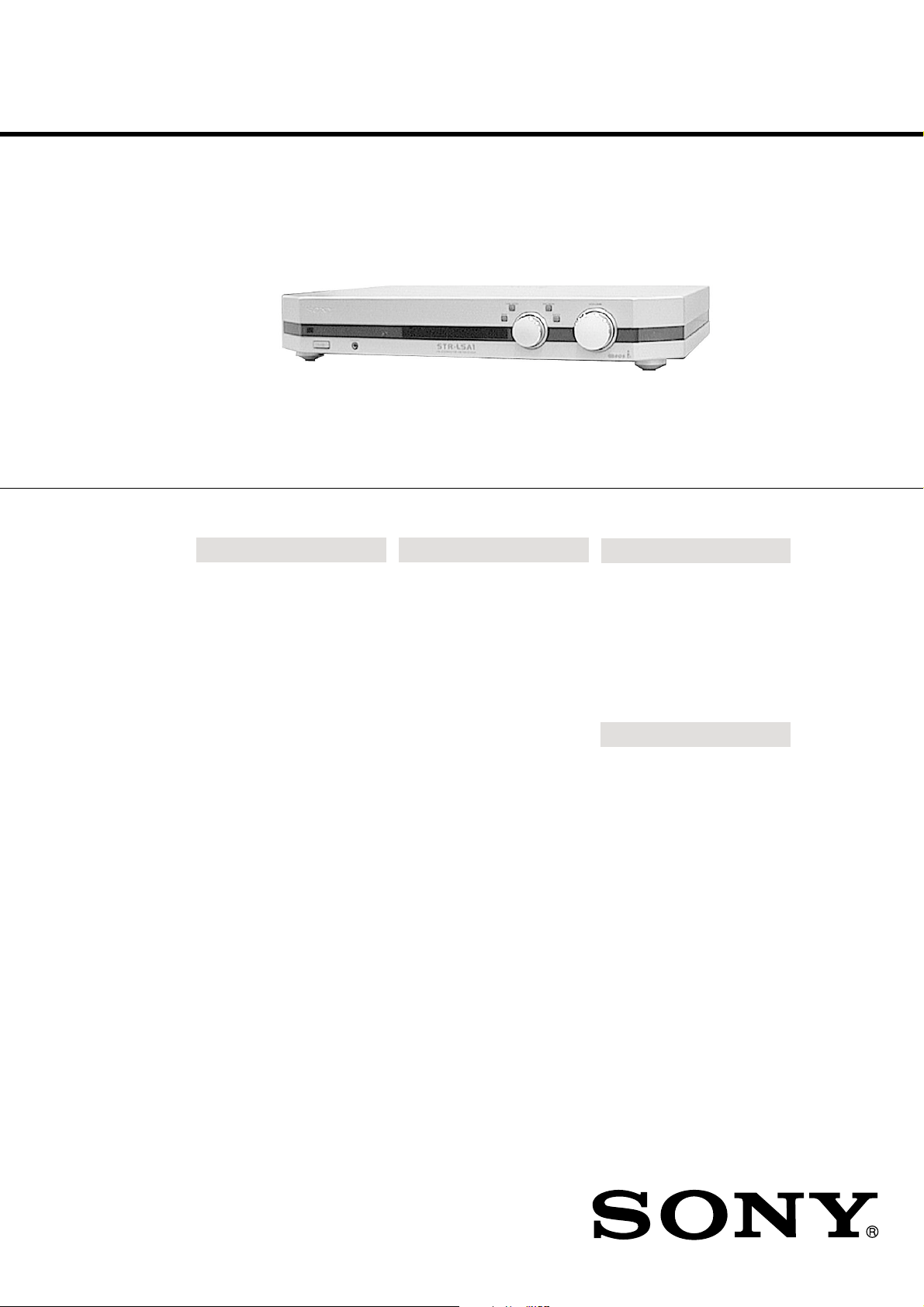
STR-LSA1
SERVICE MANUAL
SPECIFICATIONS
Amplifier section
Power output
Frequency response
Tone control
50 W + 50 W (4 ohms
DIN, 1 kHz)
7 Hz - 20 kHz ±0.3dB
Bass: 100 Hz ±10 dB
Midrange: 1 kHz
±10 dB
Treble: 10 kHz ±10 dB
FM tuner section
Tuning range
Antenna terminal
Sensitivity
THD
87.5 - 108.0 MHz
75 ohms, unbalanced
Mono: 7 µV/22.1 dBf
Stereo: 70 µV/42.1 dBf
Mono: 0.3% at 1 kHz
Stereo: 0.5% at 1 kHz
AM tuner section
Tuning range
Antenna
THD
Selectivity
Intermediate frequency
531 - 1602 kHz
Loop antenna
0.5% at 400 Hz
35 dB at 9 kHz
450 kHz
AEP Model
UK Model
Analog input
Headphone output
Sensitivity: 250 mV
Impedance: 50 kilohms
Accepts low and high
impedance
Selectivity
Separation
Intermediate frequency
55 dB at 400 kHz
35 dB at 1 kHz
10.7 MHz
General
Power requirements
230 V AC, 50/60 Hz
Power consumption
140 W
Dimensions (w/d/h)
430 × 335 × 70 mm
including projecting
parts and controls
Mass (Approx.)
6.3 kg
Supplied accessories
• AM loop antenna (1)
• Remote commander (remote) (1)
Design and specifications are subject
to change without notice.
FM STEREO FM-AM RECEIVER
Page 2
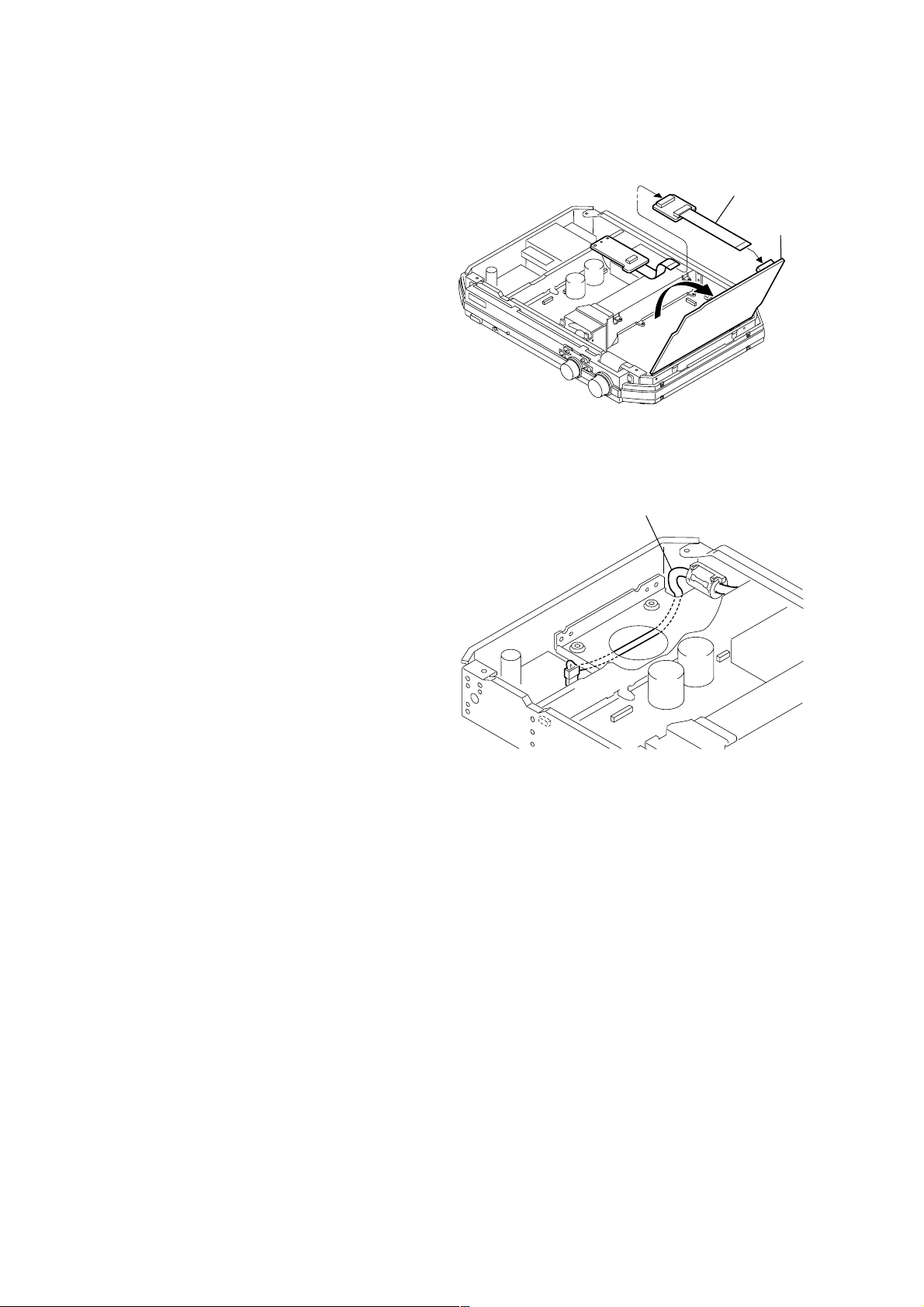
TABLE OF CONTENTS
d
SERVICE NOTE
SERVICE NOTE ····································································· 2
1. GENERAL ·········································································· 3
2. DISASSENBLY································································· 9
3. TEST MODE ···································································· 13
4. DIAGRAMS
4-1. Circuit Boards Location ·············································· 17
4-2. Block Diagram Digital Section ······························· 18
4-3. Block Diagram Main/Power Section ······················· 19
4-4. Printed Wiring Board Digital Section ····················· 20
4-5. Schematic Diagram Digital Section (1/2) ··············· 22
4-6. Schematic Diagram Digital Section (2/2) ··············· 23
4-7. Printed Wiring Board DAC Section ························ 24
4-8. Schematic Diagram DAC Section (1/2) ·················· 26
4-9. Schematic Diagram DAC Section (2/2) ·················· 27
4-10.Schematic Diagram Display Section ······················· 28
4-11.Printed Wiring Board Display Section ···················· 29
4-12.Schematic Diagram Main/Power Section················ 30
4-13.Printed Wiring Board Main/Power Section············· 31
4-14.IC Pin Function ··························································· 32
4-15.IC Block Diagrams ······················································ 33
5. EXPLODED VIEWS
5-1. MAIN SECTION ························································ 36
5-2. CHASSIS SECTION ··················································· 37
• When you want raise the DAC board in order to perform any
repair work, use the jig as shown.
Jig No.
(J-2501-009-A)
DAC boar
Note: Route the A C po wer cord making a loop so that the A C po wer cord
is routed around the screw hole.
AC power cord
6. ELECTRICAL PARTS LIST ······································· 38
SAFETY-RELATED COMPONENT WARNING!!
COMPONENTS IDENTIFIED BY MARK 0 OR DOTTED LINE WITH
MARK 0 ON THE SCHEMATIC DIAGRAMS AND IN THE PARTS
LIST ARE CRITICAL TO SAFE OPERATION. REPLACE THESE
COMPONENTS WITH SONY PARTS WHOSE PART NUMBERS
APPEAR AS SHOWN IN THIS MANUAL OR IN SUPPLEMENTS
PUBLISHED BY SONY.
Notes on chip component replacement
• Never reuse a disconnected chip component.
• Notice that the minus side of a tantalum capacitor may be
damaged by heat.
2
Flexible Circuit Board Repairing
• Keep the temperature of soldering iron around 270˚C
during repairing.
• Do not touch the soldering iron on the same conductor of the
circuit board (within 3 times).
• Be careful not to apply force on the conductor when soldering
or unsoldering.
Page 3
SECTION 1
10
GB
Front Panel Parts
Description
1 ?/1 switch
Press to turn the receiver on and off.
To avoid damaging your speakers, be sure to rotate the
VOLUME control counterclockwise immediately after
you turn on the receiver.
STANDBY indicator
Lights up when the receiver is turned off.
2 Remote sensor
When using the supplied remote, point it towards this
sensor (
).
3 SLEEP indicator
Lights up when the Sleep Timer function is activated
(page 24).
4 H.A.T.S. indicator
Lights up during H.A.T.S. (High-quality digital Audio
Transmission System) function is activated (page 25).
5 DISPLAY button
Press repeatedly to change the information in the
display window as follows:
v
Index name of the component
1)
v
Model name of the component
2)
When the built-in tuner is selected
v
Index name of the preset station
1)
or program
station name
3)
v
Frequency
1) An index name appears only if one has been assigned to the
selected component or preset station (page 22).
2) If the model name isn’t known, the category of the component
appears (e.g., “CD” or “MD”). If the category isn’t known,
“Unknown” appears.
3) Appears only during RDS reception (page 18).
When you press the DISPLAY button while the Ping
function is on, “N N n n” appears for a few
seconds in the display of the currently selected
component (page 25).
Location of
Parts
This chapter provides information
about the location and function of the
buttons and controls on the front
panel and supplied remote.
11
GB
Location kf Parts
6 Display
Shows various types of information.
7 BAND/< button
Selects the FM or AM band. If you press this button
while the receiver is turned off, the receiver
automatically turns on and tunes to the station that
was last received.
Use this button to move the cursor when entering an
index name for a component or preset station.
8 TUNE MODE/> button
When the built-in tuner is selected, press to select the
tuning mode. The mode indication appears in the
display as follows:
To select Press TUNE MODE repeatedly
to light up
Manual Tuning MANUAL
Automatic Tuning AUTO
Preset Tuning PRESET
Use this button to move the cursor when entering an
index name for a component or preset station.
9 Jog dial
Rotate to select the program source, tune to stations,
preset the stations, enter index names, or change
settings.
q; JOG MENU button
Press repeatedly to change the jog dial function. The
indication corresponding to the jog dial function
appears in the display as follows:
To Press JOG MENU repeatedly to
display
Select a component A component name
Adjust the sound Sound Menu
Make various settings Setup Menu
Receive broadcasts* Station name or frequency
*
Selectable only when the built-in tuner is selected.
After a component name appears
Rotate the jog dial to select the component you want to use.
After “Sound Menu” appears
You can use the jog dial and ENTER button to adjust the
sound (page 14).
After “Setup Menu” appears
You can use the jog dial and ENTER button to preset radio
stations (page 19), name preset stations or connected
components (page 22), or make other settings (page 24).
After a station name or frequency appears
You can use the jog dial to select a preset station (page 20) or
tune to a radio station either manually (page 18) or
automatically (page 19).
qa ENTER button
Press to enter a setting made with the jog dial.
qs VOLUME control
After turning on the selected component, rotate to
adjust the volume.
qd MUTING indicator
Lights up when the MUTING button on the supplied
remote is pressed.
qf i connector
Connects headphones. When the headphones are
connected, the kutput to the speakers is automatically
cut off.
i
I
BAND
TUNE MODE JOG MENU
ENTER
MUTING
VOLUME
STANDBY SLEEP H.A.T.S
DISPLAY
?/1
A
NM
BECD GFHJKLI
GENERAL
This section is extracted
from instruction manual.
3
Page 4
12
GB
Location of Parts
Remote Parts Description
A
Q
P
H
O
N
M
K
J
L
D
C
B
E
F
G
I
PRESET
CD
TUNER
SLEEP
SHIFT
FM MODE
DISPLAY
MD
EQ
DIMMER
FUNCTION
MID
BASS
TREBLE
EQ
BANK
VOL
MUTING
RECEIVER
BAND
?/1
–
–
+
–
+
–
+
–
+
.>
N
.>
NX x
+
+–
Xx
1 ?/1 switch
Press to turn the receiver on and off. When the
receiver is turned off, the STANDBY indicator on the
receiver turns on.
To avoid damaging your speakers, be sure to rotate the
VOLUME control on the receiver counterclockwise
immediately after you turn on the receiver.
2 FUNCTION +/– buttons
Press these buttons repeatedly to select the component
you want to use.
3 FM MODE button
If “STEREO” flashes in the display and the FM stereo
reception is poor, press this button.
“MONO” lights
up in the display and there will be no stereo effect, but
the sound will improve.
4 VOL +/– buttons
Press these buttons repeatedly to adjust the volume.
5 MUTING button
Press to mute the sound output from the receiver.
When the sound is muted, the MUTING indicator on
the receiver lights up.
6 EQ BANK button
Press repeatedly to select a preset equalizer setting.
7 TREBLE +/– buttons
After selecting preset equalizer setting, press
repeatedly to adjust the treble level.
8 MID +/– buttons
After selecting preset equalizer setting, press
repeatedly to adjust the midrange level.
9 BASS +/– buttons
After selecting preset equalizer setting, press
repeatedly to adjust the bass level.
13
GB
Location kf Parts
q; MD deck operation buttons
Use these buttons to operate a Sony MD deck.
MD N button
Press to start playback on the MD deck.
MD X button
Press to pause playback on the MD deck.
MD x button
Press to stop playback on the MD deck.
MD ./> buttons
Press to locate a track on the MD deck.
Note
This remote transmits Sony MD1 codes.
qa CD player operation buttons
Use these buttons to operate a Sony CD player.
CD N button
Press to start playback on the CD player.
CD X button
Press to pause playback on the CD player.
CD x button
Press to stop playback on the CD player.
CD ./> buttons
Press to locate a track on the CD player.
Note
This remote transmits Sony CD1 codes.
qs PRESET +/– buttons
Press repeatedly to tune in a preset station.
qd SHIFT button
Changes the memory page containing preset stations.
qf BAND button
Selects the FM or AM band. If you press this button
while the receiver is turned off, the receiver
automatically turns on and tunes to the station that
was last received.
qg SLEEP button
Press to activate the Sleep Timer function. When the
Sleep Timer function is activated, the SLEEP indicator
on the receiver lights up.
qh DIMMER button
Press repeatedly to change the brightness level of the
display.
qj DISPLAY button
Press repeatedly to select the information to be
displayed. This button has the same function as the
DISPLAY button on the receiver (5 in page 10).
4
Page 5
6
GB
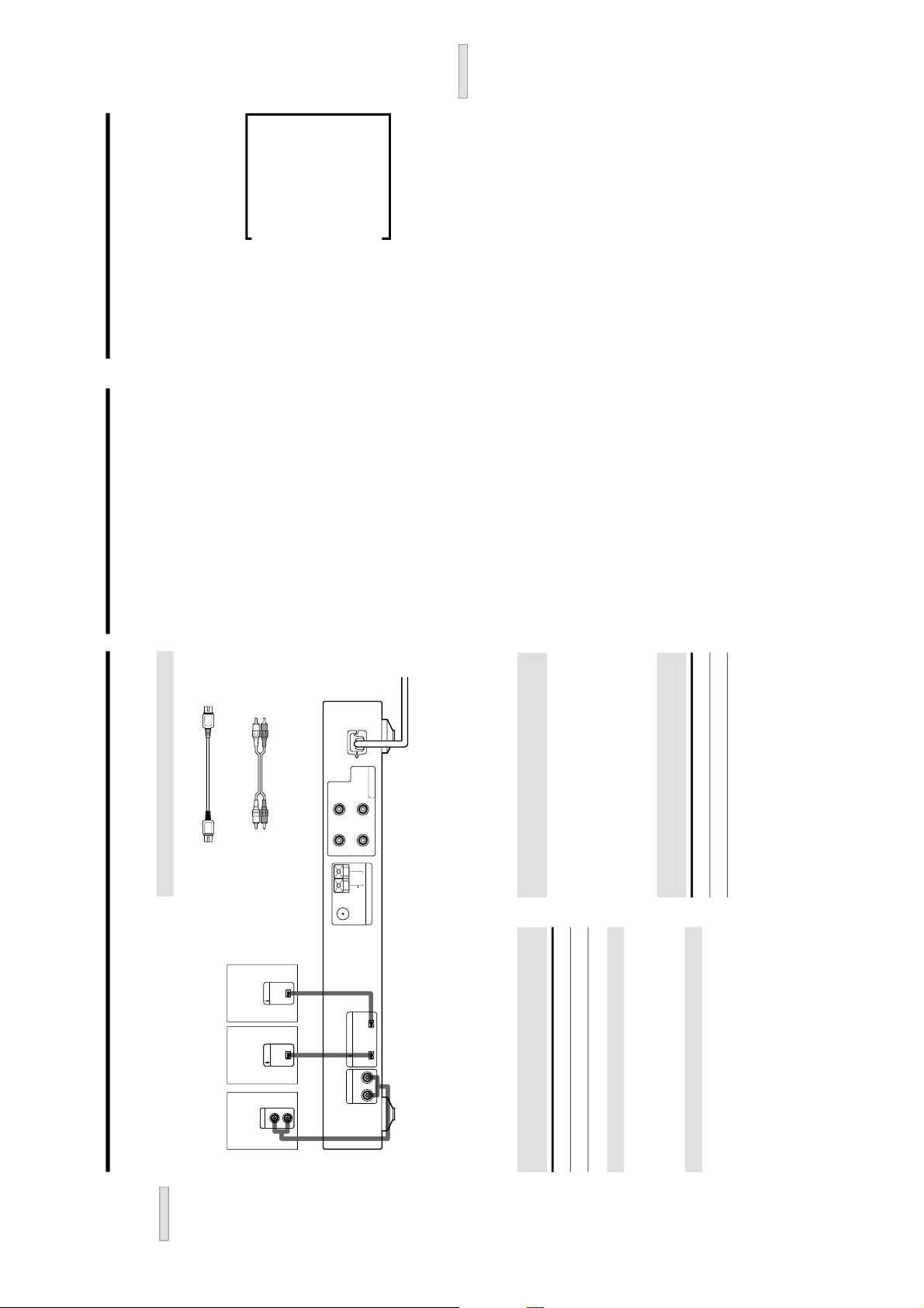
Hooking Up the System
ANTENNA
AM
SPEAKERS
IMPEDANCE
USE 4-16Ω
75
Ω
COAXIAL
FM
ANALOG IN
–
+
–
+
RL
RL
U
i.LINK S200
i.LINKi.LINK
LINE OUT
L
R
v
v
i.LINK
LINE OUT
L
R
;
;
L
CD player,
etc.*
Audio Component Hookups
Required cables
i.LINK cables (not supplied)
Audio cables (not supplied)
White (L) White (L)
Red (R) Red (R)
*
You can connect components to either i.LINK S200 connector.
Connectors for connecting i.LINK
components
Connect a To the
MD deck, CD player, etc. i.LINK S200 connector
Note on i.LINK component hookups
If a metal object should fall into the i.LINK S200
connector, short-circuiting may occur and damage the
components.
About optional i.LINK connecting cables
Be sure to use the Sony i.LINK S200 connecting cables
(4 pins-4 pins).
Tape deck,
etc.
About i.LINK components to be used in
combination with the receiver
The following i.LINK components can be used with the
receiver.
• MDS-LSA1 MD Deck
• CDP-LSA1 CD Player
z
For general information about i.LINK
See “About i.LINK” on page 26.
Connectors for connecting other audio
components
Connect a To the
Tape deck, etc. ANALOG IN connectors
MD deck,
etc.*
23
GB
Other Operations
Recording
When recording to and from the i.LINK components, you
don’t have to do any operations on the receiver. For
details, refer to the operating instructions supplied with
the playback and recording components.
Do the procedure below to record from a component
connected to the ANALOG IN connectors or from the
built-in tuner to the i.LINK MD deck. Refer to the
instruction manual of the MD deck if you need help.
1
Select the component to be recorded.
2
Prepare the component for playing.
3
Insert a blank MD into the MD deck and adjust the
recording level, if necessary.
4
Start recording on the MD deck, then start
playback on the playback component.
Note
While the MD deck is recording from a component connected to
the ANALOG IN connectors or from the built-in tuner, you can’t
select other components.
Adjusting the Brightness of
the Display
Z
You can select one of three brightness levels for the
display. The JOG MENU button can be turned off when a
low brightness level is selected.
Press DIMMER on the remote while the power is on.
Each time you press DIMMER, the brightness of the
display changes as follows:
v
The display is fully lit and the JOG MENU button is on.
v
The display lights up dimly and the JOG MENU button is on.
v
The display lights up dimly and the JOG MENU button is off.
v
The display and the JOG MENU button are both off.
z
If any change occurs in the display information while the
display is turned off
The display turns back on (dimly) for several seconds to show
the new information, and then turns off again.
z
The brightness level of the displays on the MDS-LSA1 MD
Deck and CDP-LSA1 CD Player can be linked to that of the
receiver’s display through the i.LINK Control function
The brightness level can be linked only when the i.LINK Control
function is activated. For details, see page 26.
5
Page 6

24
GB
Other Operations
Using the Sleep Timer Z
You can set the receiver to turn off automatically at a
specified time.
Press SLEEP on the remote while the power is on.
“SLEEP” lights up in the display.
Each time you press SLEEP, the time display changes as
shown below.
t 2:00 t 1:30 t 1:00 t 0:30 t 0:20 t 0:10 t OFF
After you specified the time, the display goes back the
status before you pressed the SLEEP button.
To check the remaining time before the receiver
turns off
Press SLEEP. The remaining time appears in the display.
To cancel the Sleep Timer
Press SLEEP again while the remaining time appears.
“OFF” appears in the display and the Sleep Timer is
canceled.
z
When you turn on the i.LINK Control function (see this page)
When the receiver turns off, the corresponding i.LINK
component turns off automatically at the same time.
Other Settings Using the
Setup Menu
By using the i.LINK Control function, operations on the
receiver can be automatically linked with the kperation of
specific components.
Linking receiver operations with the
operation of i.LINK components (i.LINK
Control)
When i.LINK Control is turned on, the following
operations are linked:
• When you press the CD N button or MD N button on
the remote, the receiver and the corresponding
component turn on and the component starts to play.
• When the N button on the CD player or MD deck is
pressed to start playback, or the CD N button or MD
N button on the remote of the receiver is pressed, the
respective component is automatically selected as the
program source.
• When the display brightness on the receiver is changed,
the same change occurs to the brightness level of the
displays on the MDS-LSA1 MD Deck or CDP-LSA1 CD
Player.
• When Sleep Timer turns off the receiver, the
corresponding i.LINK component also turns off.
• When you turn the receiver on or off, the corresponding
i.LINK component also turns on or off.
• When the i.LINK MD deck or CD player is selected and
no operation has been done on the receiver for more
than one minute, the receiver turns off automatically
when you turn off the selected i.LINK component.
However, when the Sleep Timer is activated, the
receiver won’t turn off until the specified time elapses.
1
Press JOG MENU repeatedly until
“Setup Menu”
appears in the display.
2
Rotate the jog dial until
“i.LINK Ctrl” appears in the
display, and then press ENTER.
3
Rotate the jog dial until
“On” appears in the
display, and then press ENTER.
To turn off the i.LINK Control function
Do the procedure above, selecting
“Of
f” in step 3.
Notes
• The i.LINK Control functions described above may not work
properly on certain components and under certain conditions.
• Make sure i.LINK Control is active on only one component
within the i.LINK configuration. For example, when two STR-
LSA1s are hooked up in the same configuration, turn on the
i.LINK Control function on only one receiver and not the other.
25
GB
Other Operations
Other Settings Using the Setup Menu
Verifying which component is currently
selected (Ping function)
When the Ping function is turned on, you can verify
which of the components is currently selected by pressing
the DISPLAY button on the receiver. An indication
momentarily appears in the display of the currently
selected component. The indication varies depending on
the component. For example, if the selected component is
either the CDP-LSA1 or the MDS-LSA1,
“N N n n” appears in the display of the
component. Note that this function works on Sony
i.LINK MD deck and CD player only.
1
Press JOG MENU repeatedly until
“Setup Menu”
appears in the display.
2
Rotate the jog dial until
“Ping” appears in the
display, and then press ENTER.
3
Rotate the jog dial until
“On” appears in the
display, and then press ENTER.
To turn off the Ping function
Do the procedure above, selecting
“Of
f” in step 3.
Improving the quality of the audio signal
(H.A.T.S. function)
When the H.A.T.S. function is turned on, digital audio
signals are momentarily stored in a buffer prior to output.
This reduces the jitter that sometimes occurs during
digital transmission. When this function is turned on, the
H.A.T.S. indicator on the front panel lights up whenever
the digital audio signal is input to the receiver.
1
Press JOG MENU repeatedly until
“Setup Menu”
appears in the display.
2
Rotate the jog dial until
“H.A.T
.S.” appears in the
display, and then press ENTER.
3
Rotate the jog dial until
“On” appears in the
display, and then press ENTER.
To turn off the H.A.T.S. function
Do the procedure above, selecting
“Of
f” in step 3.
Notes
• Due to the operating principle of the H.A.T.S. function, a slight
time lag is introduced between the initiation of an operation
(e.g., pressing the play button, stop button, or pause button)
and the actual audio output.
• The H.A.T.S. function is effective only for the components
supporting this function.
• On this receiver, the H.A.T.S. function works only with digital
audio signals with a sampling frequency of 44.1 kHz.
• The H.A.T.S. function does not work when the program source
component selected by the receiver is also selected by another
component (e.g., another receiver or the MD deck). This is
because the receiver controls the transmission rate of the digital
audio signals output from the program source component, and
for proper signal transmission, there must be only one
component which receives audio signal from a source
component within the i.LINK configuration.
• The H.A.T.S. function doesn
’t work under the following
conditions:
— When the MD is recording from the CD player, and the CD
player or the MD deck is selected as the program source.
— When the sampling frequency of the digital signal is not 44.1
kHz.
Clearing the receiver’s memory
The procedure below clears all the menu settings you
made from the receiver’s memory and restores the factory
settings.
1
Press JOG MENU repeatedly until
“Setup Menu”
appears in the display.
2
Rotate the jog dial until
“All Clear” appears in the
display, and then press ENTER.
3
Rotate the jog dial until
“Y
es” appears in the
display, and then press ENTER.
“Make Sure ?” appears in the display.
4
Rotate the jog dial until
“Y
es” appears in the
display, and then press ENTER.
6
Page 7
26
GB
Other Operations
About i.LINK
This section explains the general specifications and major
features of i.LINK. Read this section before doing any
i.LINK-related operation.
Note that i.LINK connections and operations may vary,
depending on the component. For details regarding the
connection of i.LINK components to this unit, see
“Audio
Component Hookups
” on page 6.
i.LINK functions
i.LINK is a serial digital interface that supports the
bidirectional transmission of audio and video signals,
commands, and even component status information. All
that is needed to hook up i.LINK components with i.LINK
connecting cables. Audio and video components
connected within an i.LINK configuration can be used to
perform a wide range of operations and data exchanges
that is sure to expand as the number and variety of i.LINK
components grows.
Since i.LINK allows data to be transmitted from one
component to other components to which it is not directly
connected, there is no need to pay attention to connection
order. However, due to differences in characteristics or
specifications, operation of or data exchange with certain
i.LINK components may not be possible, even when they
are connected.
z
What is i.LINK?
i.LINK is a trademark proposed by Sony Corporation and
accepted by companies throughout the world as an easy-to-
remember name for the IEEE 1394 world standard of the Institute
of Electrical and Electronics Engineers.
i.LINK connections
The use of i.LINK connecting cables to connect i.LINK
components as shown below is called a
“daisy chain”
configuration.
i.LINK connecting cable
Data can be transmitted between any two
components even if they are indirectly connected.
Branch connections
• Any i.LINK component with three or more i.LINK
connectors can serve as a branch point.
• Up to 63 i.LINK components can be connected in a
single configuration. However, the maximum number
of components that can be daisy-chained in a single
route is 17 (i.e., a maximum of 16 i.LINK connecting
cables in a row). Each i.LINK cable used in a single
route is called a “hop.” For example, ther
e are six hops
in the route between A and C in the illustration below,
and three hops in the route between A and D.
BA
DC
Each route between A and B; A and C; A and D; B and C; B
and D; and C and D in the illustration above can have 16
hops (i.e., 17 components).
Loop-connection
A signal output from one component is transmitted to all
other components. A loop connection should thus be
avoided to prevent the return of a signal to its source.
Correct Incorrect (looped)
i.LINK
component
i.LINK
component
i.LINK
component
i.LINK
component
i.LINK
component
27
GB
Other Operations
Notes
• Some i.LINK components (such as personal computers) don
’t
transfer signals when they are turned off. Refer to the
operation manual of each component to be connected before
you hook them up.
• The maximum transmission rate of an i.LINK component is
printed near its i.LINK connector. The indications S100, S200,
and S400 refer to maximum transmission rates of 100, 200, or
400 Mbps*, respectively. The actual transmission rate may be
faster or slower, depending on the differences in transmission
rates and specifications among the connected components.
z
What is Mbps?
“Mbps” is an abbreviation for megabits per second. It indicates
the amount of data transmitted per second. For example, a rate
of 200 Mbps means 200 megabits of data are transmitted in one
second.
Establishing a LINC
Before an audio signal can be transmitted between i.LINK
components, a “LINC” must first be established between
the receiving component (of the audio signal) and the
sending component. Establishing a
“LINC” means
establishing a logical path for the transmission of digital
audio signals between the two components. Each logical
path has an ID number. Since the component that sends
an audio signal must output the signal to a path, and the
component that receives the signal must input it from the
same path, the path must be mutually known by both
components. During the establishment of a LINC, the
following communication occurs between the two i.LINK
components.
Example
A component establishing a LINC with a CD player in
order to receive an audio signal from the CD player
1 The component that will receive an audio signal
from the CD player sends a request and path
information to the CD player to establish a
transmission path for the audio signal.
1
,
2
<
2 The CD player responds to the component, agreeing
to the establishment of a LINC.
The digital audio signal transmission becomes possible
only after the communication described above has
occurred and a LINC has been established.
The component
that receives
the audio signal
CD player
(sending
component)
7
Page 8

31
GB
Additional Information
Display Messages
The following table explains the various messages that appear in the display.
Message Error code(s) Cause and/or remedy
CANNOT LINC C78:11/C78:12 The receiver can’t establish a LINC with a component because of an existing LINC between
the receiver and another component. Cancel the LINC between the receiver and the other
component.
NO SIGNAL C78:04 No signal is output from the selected component. Verify that the signal is output from the
component (e.g., by recording from the component).
C78:22 The format of the input signal is not supported.
C78:31 The communication between the receiver and the selected component is unstable. Or, the
format of the input signal is not supported. Check the condition and the signal format of
the selected component.
BUS FULL C78:15 The signal bus within the i.LINK configuration is full and no more signals can be output
from the receiver. Cancel the LINC between the component and the receiver.
LOOP CONNECT C78:03 The i.LINK connection is looped. Check the connection (see page 26).
NEW CONNECT — An i.LINK component has been connected to or disconnected from the i.LINK
configuration. Wait several seconds for the indication to turn off.
FUNC. Locked — You can’t select a component because the LINC between the other component and the
receiver is currently established. Cancel the LINC between the other component and the
receiver.
Select FUNC. — Select another component.
Input Occupied Cancel the LINC between the other component and the receiver.
Off Processing — While the i.LINK Control function is activated, the corresponding i.LINK component turns
off automatically when you turn off the receiver. However, it may take a while for the
component to turn off and no operations are possible on the receiver while this indication
is flashing. Wait several seconds for the indication to turn off.
8
Page 9
SECTION 2
s
DISASSENBLY
Note : Follow the disassembly procedure in the numerical order given.
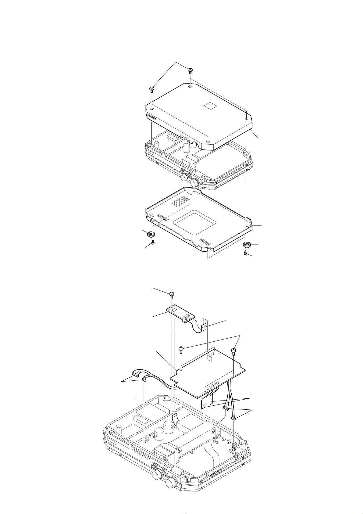
2-1. TOP CASE
2 Two foot assy's
4 Four screws (CASE)
5 Top case
3 Bottom case
1 Two screws
(BVTP 3 × 8)
2-2. RDS BOARD AND DAC BOARD
7 Screw
(BVTP 3 × 8)
8 RDS board
5 DAC board
4 Connectors
(CN752, CN753)
2 Two foot assy'
1 Two screws
(BVTP 3 × 8)
6 Flat type wire
(CN303)
1 Four screws
(BVTP 3 × 8)
2 Flat type wires
(CN104, CN105)
3 Connectors
(CN101, CN108)
9
Page 10
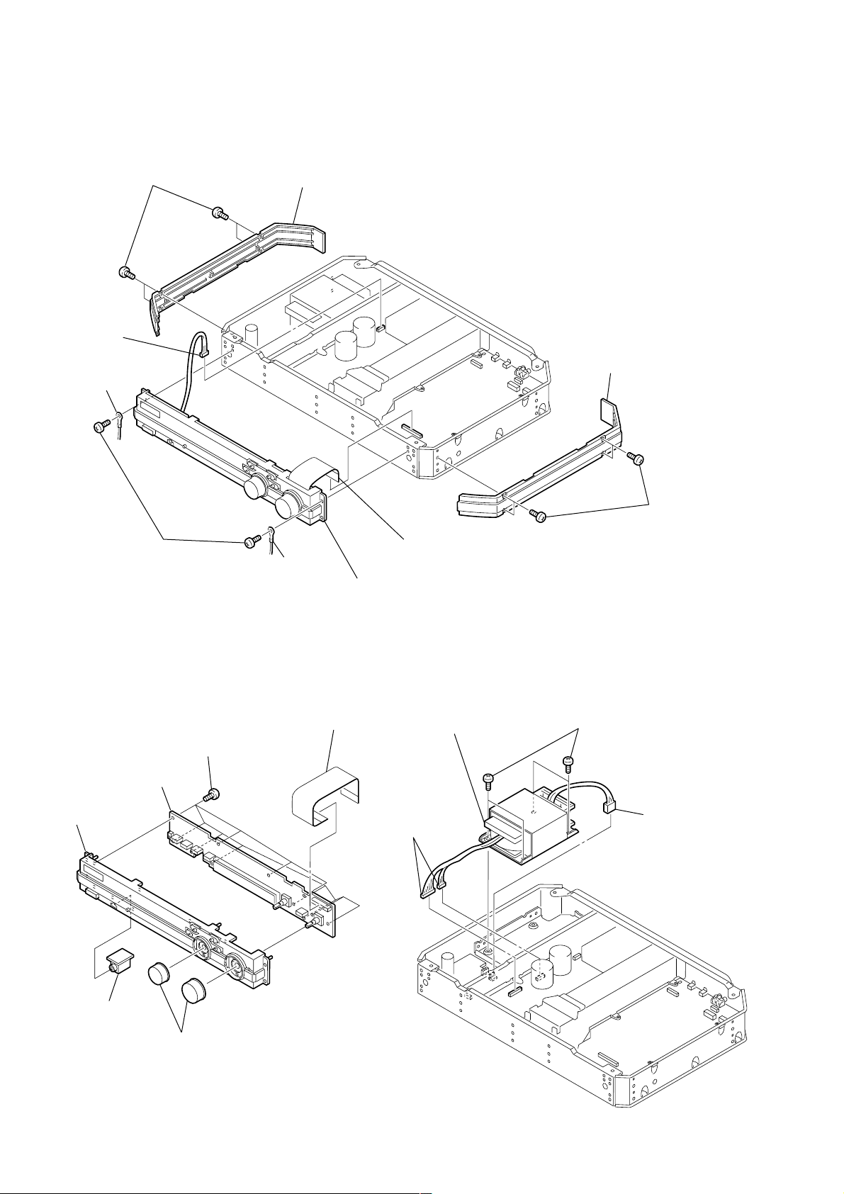
2-3. PANEL BASE ASSY
l
1 Four screws
(BVTP 3 × 8)
5 Connector
(CN503)
8 Lug
7 Two screws
(TP), Flat head
2 Plate (side), ornamental
8 Lug
9 Panel base assy
4 Plate (side), ornamenta
3 Four screws
(BVTP 3 × 8)
6 Flat type wire
(CN107)
2-4. DISPLAY BOARD
4 DISPLAY board
6 Panel base
5 HP board
1 Knob assy
2 Eleven screws
(BVTP 2.6 × 8)
3 Flat type wire
(CN801)
2-5. POWER TRANS (T2)
4 Power Trans (T2)
1 Connectors
(CN2, CN4)
3 Four screws
(BVTT 4 × 6)
2 Connector
(CN3)
10
Page 11
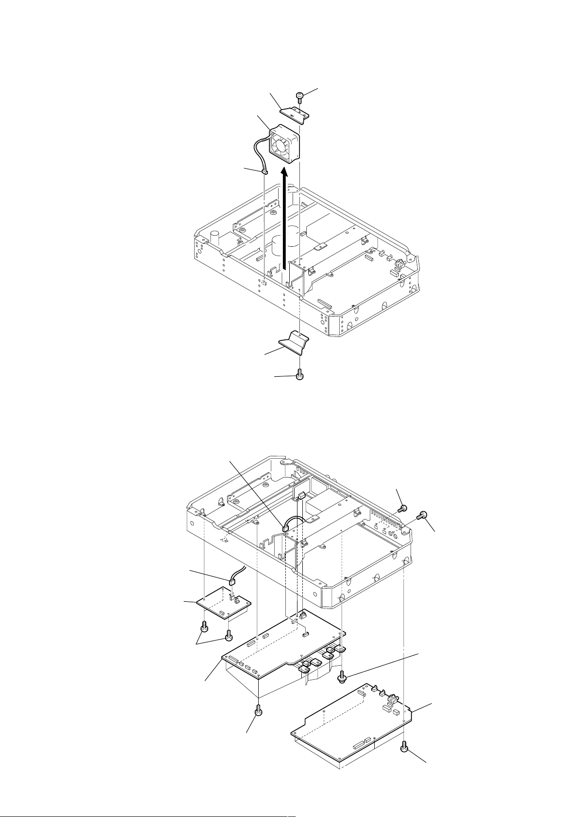
2-6. DC FAN (M1)
d
5 Duct cover (T)
6 DC fan (M1)
3 Connector
(CN8)
2 Duct cover (B)
4 Screw
(BVTP 3 × 8)
1 Screw
(BVTP 3 × 8)
2-7. PS BOARD, MAIN BOARD AND DIGITAL BOARD
6 Connector
(CN506)
2 Connector
(CN3)
3 PS board
1 Four screws
(BVTP 3 × 8)
8 Two screws
(BVTT 2.6 × 6)
9 Screw
(BVTP 3 × 8)
5 Six screws
(Transistor)
7 MAIN board
4 Six screws
(BVTP 3 × 8)
qa DIGITAL boar
0 Six screws
(BVTP 3 × 8)
11
Page 12
2-8. TS BOARD
l
2-9. SP BOARD
1 Screw
(BVTP 3 × 8)
2 Bracket
3 TS board
2 Cord bushing and AC power cord
7 SP board
1 Three screws
(BVTP 3 × 8)
4 Screw
(BVTP 3 × 10)
3 Five screws
(BVTP 3 × 8)
5 Two screws
(BVTP 3 × 8)
6 Tuner
8 Rear pane
12
Page 13
SECTION 3
TEST MODE
1. How to Enter the Test Mode
Press the three buttons of JOG MENU , DISPLAY and ?/1 at the same time in the STANDBY mode to enter the test mode.
2. How to Exit the Test Mode
Press the ?/1 button to enter the STANDBY mode and the machine exits the test mode.
3. Structure of the Test Mode
The test mode consists of the following ten test items.
Rotate the JOG dial to move to each test item.
However, structure of the test items is not looped. Therefore, direct movement between Version Check and All Clear items is not possible.
1) Version Check
2) CID Check
3) Volume Set
4) Key Check
5) FL/LED Check (All)
6) FL/LED Check (Type1)
7) FL/LED Check (Type2)
8) Factry Preset
9) i.LINK Check
10) All Clear
4. Contents of Each Test Mode
1) Version Check
Indicates the version number of the ROM.
2) CID Check
Indicates the ID information of the configuration ROM inside the Node Unique ID.
3) Volume Set
The volume control value can be set in four steps by every pressing of the ENTER button as follows.
“Vol.Set -∞ dB”→“Next Ent. Max ! ”(-40dB)→“Vol.Set 0dB”→“Vol.Set -20dB”→.....
4) Key Check
When the machine enters the Key Check mode, the following message appears on the display.
“Rest 05Key”
When any button other than the ?/1 button is pressed, the number decreases. When all b uttons are pressed, the number becomes “00”.
5) FL/LED Check (All)
When the machine enters the FL/LED Check (All) mode, all FL displays and LED displays turn on.
6) FL/LED Check (Type 1)
When the machine enters the FL/LED Check (Type 1), the LEDs of STANDBY, SLEEP and JOG MENU turn on and the FL display
shows the following message.
Fig. 1 FL/LED Check (Type 1)
7) FL/LED Check (Type 2)
When the machine enters the FL/LED Check (T ype 2), the LEDs of HATS, DISPLAY and MUTING turn on and the FL display shows
the following message.
Fig. 2 FL/LED Check (Type 2)
8) Factory Preset
When the Enter button is pressed while the message “Factory Preset” being displayed, the following frequencies are pre-set to the six
pre-set stations A1 to A6 of the tuner. You can check the frequencies by rotating the JOG dial.
A1: FM 88.00 MHz
A2: FM 98.00 MHz
A3: FM 106.00 MHz
A4: AM 603 kHz
A5: AM 999 kHz
A6: AM 1404 kHz
When the ENTER button is pressed again, the message returns to the Factory Preset.
13
Page 14

9) i.LINK Check
When the DISPSLAY button is pressed while the message “i.LINK Check” is being displayed, the machine enters the i.LINK TEST
mode.
The initial display is “<[BACK]>”. When the DISPLAY button is pressed while the initial display is being shown, the message returns
to the i.LINK Check display.
The i.LINK TEST mode contains the total of 90 test items. You can select the desired test item by rotating the JOG dial. (See next page.)
Note that the i.LINK TEST items other than the followings are not used in service.
No.5 Bus reset counter
Indicates the total numbers of the bus reset that are detected until the present time.
Press the DISPLAY button to reset the counter to 0.
How to use this test item:
When a new equipment is connected or removed, the bus reset occurs.
Using this characteristics, confirm that the connectors have no poor contact or that the cables are not open by conf irming
the numbers of bus reset.
No.7 Async packet reception counter
Indicates the total numbers of the Async packet that have been received up to the present time except Ack.
Press the DISPLAY button to reset the counter to 0.
How to use this test item:
When the machine receives a command from other equipment, the counter increments.
Using this characteristics, confirm that the commands are correctly received or not.
Let other equipment send the commands and confirm hat the counter increments using the Ping function.
T o inter the i.LINK TEST mode, there are two methods. One is to enter the i.LINK TEST mode from the test mode. The other is to enter
the i.LINK TEST mode directly that is described as follows.
1. Press the JOG MENU button while the main power is on. Select the Sound Menu.
2. The display changes to “EQ BANK”. Press the ENTER button. Then the display changes to “EQ1”.
3. When the ENTER button is kept pressed in this condition, the machine enters the i.LINK TEST mode.
When the same procedure as described above is performed while the machine is in the i.LINK TEST mode, the machine exits the i.LINK
TEST mode.
In the same manner, when the machine has entered the i.LINK TEST mode directly, press the DISPLAY button while the <[B A CK]> is
being indicated. Then the machine returns to the i.LINK Check indication from which you the machine can move to an y other test mode
item.
10) All Clear
When the ENTER button is pressed while the message All Clear is being displayed, the various settings are returned to the default
settings when shipped from the factory.
The display turns off for a moment, the message “All Clear!” appears and the machine exits the test mode to return to the Power on
status.
14
Page 15
Display 3
(itest_disp = 2)
< [BACK] >
Display 1 Display 2
(itest_disp = 0) (itest_disp = 1)
FUNCTION indication
FUNCTION indication
FUNCTION indication
FUNCTION indication
FUNCTION indication
Forceroot
Ver. xxxxxx
Root Yes(No)
B.Rst [xxx]
NID. xxxx/xx
FUNCTION indication
FUNCTION indication
FUNCTION indication
FUNCTION indication
FUNCTION indication
G.C [xx]
Async [xxx]
State BR 0000 zzzzzzzz
Node IDR 0008 zzzzzzzz
Split THR 0018 zzzzzzzz
FUNCTION indication
FUNCTION indication
FUNCTION indication
FUNCTION indication
FUNCTION indication
Split TLR 001C zzzzzzzz
Bus TR 0204 zzzzzzzz
Busy TR 0210 zzzzzzzz
Bandwidth AR 0220 zzzzzzzz
Channel AHR 0224 zzzzzzzz
FUNCTION indication
FUNCTION indication
FUNCTION indication
FUNCTION indication
FUNCTION indication
Channel ALR 0228 zzzzzzzz
Output MPR 0900 zzzzzzzz
Output PCR 0904 zzzzzzzz
Input MPR 0980 zzzzzzzz
Input PCR 0984 zzzzzzzz
FUNCTION indication
FUNCTION indication
FUNCTION indication
FUNCTION indication
FUNCTION indication
NUID 08004605> NUID <005zzzzz
i.LINK IC [zz] 00zz zzzzzzzz
rid:0-6 m:0-5 HATS:0-3
errcode:NOERR/EMPTY/UNLCK/DIRER/FREQ
ConnectStatus:0-3, SelectStatus:0-2
FUNCTION indication
FUNCTION indication
FUNCTION indication
FUNCTION indication
FUNCTION indication
difConnectFlag, LockFlag
DIF_CONNECT_INFO_FLAG_NAME
DIF_CONNECT_REQ_FLAG_NAME
DIF_CONNECT_REF_FLAG_NAME
DIF_CONNECT_REF_OPCR_FLAG_NAME
x: decimal number, z: hexadecimal number
Contents that are executed
Display Items
No.
STR i.LINK Test Mode
by pressing the DISPLAY button
Switching between “i.LINK Check” ⇔ ”< [BACK] >”
(Selected by JOG)
< [BACK] >
0
(itest_no)
Nothing is executed
Nothing is executed
Firmware version
Root display
1
2
Nothing is executed
Bus reset is performed
Counter value is returned to 0
Nothing is executed
Node ID and numbers of connected device
Bus reset is generated
Bus reset counter
Gap count
3
4
5
6
Counter value is returned to 0
Three indications in the right are switched.
Three indications in the right are switched.
Three indications in the right are switched.
Three indications in the right are switched.
Three indications in the right are switched.
Three indications in the right are switched.
Three indications in the right are switched.
Three indications in the right are switched.
Async packet reception counter
Register, State Bits Register
Register, Node ID Register
Register, Split Timeout Hi Register
Register, Split Timeout Low Register
Register, Bus Time Register
Register, Busy Timeout Register
Register, Bandwidth Available Register
Register, Channel Available Hi Register
7
8
9
10
1112131415
Three indications in the right are switched.
Three indications in the right are switched.
Three indications in the right are switched.
Three indications in the right are switched.
Three indications in the right are switched.
Three indications in the right are switched.
Three indications in the right are switched.
Two indications in the right are switched.
Two indications in the right are switched.
Two indications in the right are switched.
Register, Channel Available Low Register
Register, Output Master Plug Register
Register, Output Plug Control Register
Register, Input Master Plug Register
Register, Input Plug Control Register
Node Unique ID
LINK IC Register [00] to [FC]
Debug information (recidstep,mutsts,HatsStatus)
Debug information (Digital signal status, errcode)
Debug information (Input Select module information)
1617181920
21
828384
22 to 81
Two indications in the right are switched.
Two indications in the right are switched.
Two indications in the right are switched.
Two indications in the right are switched.
Two indications in the right are switched.
Debug information (Stream Manager information )
Debug information (Stream Manager information )
Debug information (Stream Manager information )
Debug information (Stream Manager information )
Debug information (Stream Manager information )
8586878889
15
Page 16

Contents
63 devices are selected and LINK is connected. No more devices are allowed.
63 STRs are selected and LINK is connected. No more STRs are allowed.
Unsupported format (The signal that cannot be played back) is detected.
The signal clock is outside the specifications and the PLL lock is being lost.
When any input signal is not connected when the i.LINK device is selected.
Bus is filled with signals so that input and output are disabled.
A signal loop is formed by the i.LINK cable.
A bus reset is generated. (For example when a new device is connected.)
Indicated during the i.LINK test mode
12 PtoP has failed.
31 PtoP has failed.
22 This is not IEC958 Conf.
23 N bit is different.
25 Frequency is different.
26 This is not linear PCM.
Error code number
C78:11 (When the i.LINK device is selected)
C78:12 (TUNER, ANALOG)
C78:22
Message on display
CANNOT i.LINK
CANNOT i.LINK
STR i.LINK Error Message
NO SIGNAL
16
24 PLL is unlocked
21 No signal
C78:31
C78:04
NO SIGNAL
NO SIGNAL
13 Bandwidth is not sufficient during input.
14 Channels are filled during input.
15 Bandwidth is not sufficient during output.
C78:15
BUS FULL
33 Channels are filled during output.
C78:03
Error code number is not allocated yet.
LOOP CONNECT
NEW CONNECT
Page 17

SECTION 4
d
1 IC52 qf (XO)
1.85Vp-p
(4.33 MHz)
0.24 µsec
1 IC301 eg (XOUT)
44 nsec
6 Vp-p
(22 MHz)
DIAGRAMS
THIS NOTE IS COMMON FOR PRINTED WIRING BO ARDS AND SCHEMATIC DIAGRAMS.
(In addition to this, the necessary note is printed in each bloc k.)
Note on Schematic Diagram:
• All capacitors are in µF unless otherwise noted. pF: µµF
50 WV or less are not indicated except for electrolytics
and tantalums.
• All resistors are in Ω and 1/
specified.
f
•
• 2 : nonflammable resistor.
• 5 : fusible resistor.
• C : panel designation.
The components identified by mark 0 or dotted
line with mark 0 are critical for safety.
Replace only with part number specified.
• U : B+ Line.
• V : B– Line.
• V oltages are taken with a VOM (Input impedance 10 MΩ).
• Waveforms are taken with a oscilloscope.
• Signal path.
: internal component.
Voltage variations may be noted due to normal production tolerances.
Voltage variations may be noted due to normal production tolerances.
F : TUNER
4
W or less unless otherwise
Note on Printed Wiring Boards:
• X : parts extracted from the component side.
• b : Pattern from the side which enables seeing.
Caution:
Pattern face side: Parts on the pattern face side seen from
(Side A) the pattern face are indicated.
Parts face side: Parts on the par ts face side seen from
(Side B) the parts face are indicated.
• Indication of transistor.
C
These are omitted.
Q
B
CE
These are omitted.
Q
B
E
• WA VEFORMS
— RDS BOARD —
— DAC BOARD —
— DIGITAL BOARD —
1 IC109 es (XO)
(24.576MHz)
40 nsec
2.6 Vp-p
2 IC114 qd (XOUT)
(10MHz)
0.1µsec
3.5 Vp-p
4-1. CIRCUIT BOARDS LOCATION
SENSOR board
POWER board
DISPLAY board
HEADPHONE JACK board
SPEAKER TERMINAL board
RDS board
MAIN board
DAC boar
DIGITAL board
1717
Page 18

STR-LSA1
4-2. BLOCK DIAGRAM DIGITAL SECTION
PHY
IC109
TB2N
49
TB2P
|
TA2N
52
TA2P
TBIAS2
46
TB0N
57
TB0P
|
TA0N
60
TA0P
48
TBIAS0
XI
33
32
XO
PLL
IC119
DATA0
DATA3
CTL1
CTL0
SCLK
LREQ
VCOO
|
FINB
FINA
13
14
16
17
11
10
8
6
5
4
3
i.LINK S200
POWER RY
CN102
CN103
E
[POWER]
TB2N,TB2P,TA2N,TA2P
BIAS
Q101,102
TB0N,TBOP,TAON,TAOP
BIAS
Q103,104
X101
24.576MHz
BIAS-ON
77
|
74
79
80
83
81
25
26
27
D0-D15
2-5,7-10
41-44,46-49
143-136,134-127
DT0-DT15
D0-D3
CTL1
CTL0
SYSCLK
LREQ
1/8OUT
SYTO
PLLCKI
DATA0-DATA15
XRESET
54-47,45-38
85
DRAM
IC122
A0-A9
21-24,27-32
121-117,115-111
A0-A9
AUDIO-LINK
IC117
A0-A7
63-70
XWE
XOE
33 34 35
17
18
124
125
122 123
XOE
XWE
XRDY
XRD
61 59 58 57
XRAS
XRAS
DOUT
DATA0
BCKO
LRCKO
512FSI
XWR
XUCAS
XCAS
EOF
DIN
XCS
XLCAS
18
23
22
20
21
2
17
IC317
GATE
Q105
14
2
7
11
P/SW
IC106
6A
4A 4Y
1A
3Y
5Y
G1
G2
1,15
DIR
IC111
13
6Y
XMOD(DIR)
SCK(DIR)
XLT(DIR)
SWD(DIR)
910
3
1Y
542A 2Y
3A
6
12
5A
1
2
10
14
15
16
DIN1
DIN2
XMOD
SCK/CL
XLT/CE
SWDT/DI
DOUT
BCK
LRCK
FS128
AVCK
ERR
SRDT/DO
IC108
23
21
22
20
11
24
17
INIT(SRC)
SRC
IC107
1
DOUT
3
BCK
2
LRCK
7
FS128
10
INIT
15
DO1
DIT
IC103
DATAO
LRCKO
DATA
BCK
LRCK
BCKO
XI
30
31
32
13
XI
6
5
4
13
IC110
IC104
IC110
IC110
SIA
117
DSP
IC101
SIB
118
SIC
IC105
3
2
6
5
4
7
1
119
113
114
115
116
BCK0
BCK1
LRCK0
LRCK1
16-20,23-25
HD0-HD7
XHDWR
CLKI(256FS)
XHDWR
XHDRD
XHDCS
9 10 14 15
XHDCS
XHDRD
HRDY
HA0
HA0
SOA
SOD
26
X RST
XRST
2
5
13
IC102
99
1/2
PROTECT
C
[RDS]
D
[MAIN]
16
51
31
BIAS-ON
PROTECT IN
E2PROM
IC116
6
29
IIC CLOK
BCK(DAC)
ADDATA
256FS
IC118
RESET GEN
5
30
IIC DATA
3
12
RESET
X102
10MHz
13 15
XOUT
XIN
88-73 72-65
D0-D15
1394RSET
A0-A7
46 49
3932
44
RD
WR
RDY
SYSTEM CONTROL
CSI
IC114
SIRCS IN
KEY2
KEY1
ENC B
ENC A
POW KEY
VOL-A
ENCODER B
ENCODER A
POWER KEY
VOL-B
VOL-A
VOL-B
DATA
SEL
11
35
10 34
DIR-IN
ERR
36 37
FL DATA
FL C-SEL
CLK
FL CLOK
22
21
SOD(DSP)
HRDY(DSP)
L MUTE
LINE MUTE
DOP0
|
DOP7
OE
LATCH5
LATCH4
LATCH3
LATCH2
LATCH1
7
|
1
100
23
24
25
26
27
28
CLK(VOL)
LATCH(DAC)
SHIFT(DAC)
INIT(DAC)
ATT(DAC)
18
19
16 15 14
17
1Q2Q3Q4Q5Q6Q7Q
IC115
1D-8D
OE
2-9
1 11
BS(VOL)
DI(VOL)
13
CLK
RDS CLK
RDS DATA
TUNED
STEREO
D IN
525354 90
TUNED
STEREO IN
RDS DATA-IN
S-METER
ST DATA IN
SIGNAL LEVEL
50
939495 97 48 47
92
SIRCS IN
A/D KEY2
A/D KEY1
TUN MUTE
38
POWER RY
18
20
33
RDS CLK-IN
TUNER MUTE
LRCK(DAC)
INIT(SRC)
ATT
CLK-ST
XHDRD
18
16 15 14
17
2Q3Q4Q5Q6Q
IC113
1D-8D
2-9
CLK-SEL
DATA-ST
CE-ST
12
13 1218
7Q
OE
CLK
1 11
HD0-HD8
12-19
1Q-8Q
8Q
IC112
1D-8D
OE
2-9
1 11
SWD(DIR)
19
1Q2Q3Q4Q5Q6Q7Q
CLK
XLT(DIR)
1D-8D
SCK(DIR)
XMOD(DIR)
16 15 14
17
IC121
2-9
XHDWR
XHDCS
OE
1 11
HA0
13
CLK
512FS
X RST
8Q
DATA(DAC)
LED1
LED2
LED3
LED4
LED5
16 15 14
19
17
1Q2Q3Q4Q5Q6Q7Q
IC120
1D-8D
OE
2-9
1 11
FL RES
TUNER/AUX
13
CLK
ANA INH
1218
8Q
B
[DAC]
A
[DISPLAY]
1818
Page 19

4-3. BLOCK DIAGRAM MAIN/POWER SECTION
STR-LSA1
ANALOG IN
ANTENNA
INPUT
J101
L
R
R-CH
TUNER/AUX
ANA INH
Q304
Q303
SELECTOR
12
X0
X1
14
10
A
6
INH
IC310
IC308
13
X
UNBAL BAL
DATA(DAC)
BCK(DAC)
LRCK(DAC)
INIT(DAC)
ATT(DAC)
SHIFT(DAC)
LATCH(DAC)
B
A
DRIVER
TUNER UNIT
L CH
R CH
FM
AM
FM DET OUT
D O
FMIF OUT
TUNED
STEREO
CE
DATA
CLOCK
MUTING
X52
4.33MHz
R-CH
13
14
4
MUTING
Q307,308
RDS
IC52
16
2
RDSCLK
RDSDATA
DIN
S-METER
TUNED
STEREO
CE-ST
DATA-ST
CLOCK-ST
TUN-MUTE
DATA
CLK
SEL
FL RES
–29V
LED2
LED4
LED1
LED3
IC861
63
DAT
62
CLK
61
CS
60
RST
V FL
56
C
AD/DF/DAC
IC301
IC317
98
56
11 10
13 12
MUTING
DISPLAY
STANDBY
SELECT
34
12
D843
SLEEP
D846
D844
D845
FLOW
D847
D841
JOG
CLK(VOL)
DI(VOL)
BS(VOL)
INIT(DAC)
41
56
INLP
55
INLM
27
DADT
11
BCK1
26
BCK2
10
LRCK1
28
LRCK2
16
DPD
18
INIT
19
MODE
20
SHIFT
21
LATCH
FL
40
G1
54
G15
S1
5
S35
39
P1
1
2
P2
+L1
–L2
XIN
XOUT
ADDT
MCK1
256CK
512CK
G1-G15 S1-S35
VF1
LED SW
Q843
LED SW
Q846
LED SW
Q844
LED SW
Q845
LED SW
Q847
LED SW
Q841
39
36
35
12
15
22
25
FL TUBE
FL801
2
IC302
X301
22MHz
ADDATA
4
VF2
256FS
512FS
+3.3V
(SW)
+3.3V
(EVER)
+12V
18
IN1+R
17
IN1–R
IN2+R
20
IN2–R
21
IC306
8
CLK
9
DI
10
BS
11
RES
KEY1
KEY2
POWER KEY
VOL A
VOL B
ENC A
ENC B
SIRCS IN
IDAC
IC303
6
IOR+
5
IOR–
CIREF
1
I-AMP
13
VOUT1
VOL
IC307
BAND ENTER TUNING JOG MENU
S806
DISPLAY
S801
I/u
RV801
VOL
RV802
JOG
IC881
1
SIRCS
BAL UNBAL
L-MUTE
ATT
DRIVER
Q305,306
DRIVER
Q311,312
S804S803S802S805
• Signal Path
TUNER :
• R-CH is omitted.
POWER AMP
IC501
IC314(1/2)IC312,314(2/2)
6
FAN
ATT
Q309
+5V
+5V
+3.3V
(SW)
IN1
Q706,707
3 1
3 1
+3.3V(EVER)
LPF
R-CH
MUTE
Q301
R-CH
IC301
IC307
IC317
IC318
D101-104
+VOUT1
–VOUT1
OVERHEAT DET
SWITCH
IC305
+5V
REG
+6V
–6V
+12V
IC756
+3.3V
REG
NF1
IC502
2
5
3
R-CH
–29V
+10V
OUTPUT
DRIVER
Q502-504
OVERLOAD DET
Q505
Q700
-29V REG
Q703
IC751
+10V
3 1
REG
IC752
+6V
3 1
REG
IC753
–6V
3 2
REG
IC754
+12V
3 1
REG
IC755
+5V
3 1
REG
IC757
+3.3V
3 1
REG
+15.5V
–15.5V
+39V
–39V
R-CH
IC700
1
OVER LOAD
2
DC
8
VCC
7
ON-MUTE
4
AC-OFF
SPEAKER DET
D509,725
AC DET
D700
D750
RELAY
D751
D801-804
6
D702-705
D727
RY501
43
R-CH
R-CH
RY502
T2
D729D728
D730
F701
F702
VF1
VF2
F703
T1
RY1
TM501
BUFFER
Q701,702
Q705
L
SPEAKERS
R
J501
PHONES
PROTECT
D
POWER RY
E
F1
AC IN
16
1919
Page 20

STR-LSA1
4-4. PRINTED WIRING BOARD DIGITAL SECTION
• Semiconductor
Location
Ref. No. Location
D101 E-9
D102 F-9
D103 E-9
D104 F-9
IC118 C-9
Q101 F-9
Q102 F-9
Q103 G-9
Q104 G-9
• See page 17 for Circuit Boards Location.
(Page 24) (Page 24)
There are a few cases that the part printed on
this diagram isn’t mounted in this model.
(Page 24)
(Page 29)
(Page 24)
2020
Page 21

There are a few cases that the part printed on
this diagram isn’t mounted in this model.
STR-LSA1
• Semiconductor
Location
Ref. No. Location
IC101 C-6
IC102 C-6
IC103 F-6
IC104 B-7
IC105 C-7
IC106 E-6
IC107 F-8
IC108 F-8
IC109 F-2
IC110 C-8
IC111 F-7
IC112 B-3
IC113 B-2
IC114 D-3
IC115 B-1
IC116 C-1
IC117 F-4
IC119 F-4
IC120 B-4
IC121 B-3
IC122 G-3
IC317 F-6
Q105 E-6
2121
Page 22

STR-LSA1
4-5. SCHEMATIC DIAGRAM DIGITAL SECTION (1/2)
2222
Page 23

4-6. SCHEMATIC DIAGRAM DIGITAL SECTION (2/2)
STR-LSA1
PIN FUNCTION
✩
✩
This is a written EEPROM. Not supplied in independently
but is supplied as the DIGITAL BOARD, COMPLETE.
2323
Page 24

STR-LSA1
4-7. PRINTED WIRING BOARD DAC SECTION
• Semiconductor
Location
Ref. No. Location
D101 C-9
D102 C-9
D103 D-8
D104 C-9
D301 E-8
IC305 E-7
IC307 F-8
Q301 C-3
Q302 D-3
Q305 C-2
Q306 C-2
Q309 C-3
Q310 D-3
Q311 C-2
Q312 C-2
(Page 31)
(Page 31)
(Page 20)
• See page 17 for Circuit Boards Location.
There are a few cases that the part printed on
this diagram isn’t mounted in this model.
(Page 20) (Page 20)
(Page 31)
(Page 29) (Page 20)
2424
Page 25

There are a few cases that the part printed on
this diagram isn’t mounted in this model.
STR-LSA1
• Semiconductor
Location
Ref. No. Location
IC301 D-2
IC302 B-2
IC303 C-4
IC306 F-3
IC308 F-5
IC309 G-5
IC310 F-6
IC312 C-6
IC313 D-6
IC314 C-7
IC315 D-7
IC317 C-3
IC318 D-3
Q303 F-6
Q304 F-6
Q307 G-9
Q308 G-9
2525
Page 26

STR-LSA1
4-8. SCHEMATIC DIAGRAM DAC SECTION (1/2)
2626
Page 27

4-9. SCHEMATIC DIAGRAM DAC SECTION (2/2)
STR-LSA1
2727
Page 28

STR-LSA1
4-10. SCHEMATIC DIAGRAM DISPLAY SECTION
2828
Page 29

STR-LSA1
(Page 20)
4-11. PRINTED WIRING BOARD DISPLAY SECTION
• See page 17 for Circuit Boards Location.
There are a few cases that the part printed on
this diagram isn’t mounted in this model.
• Semiconductor
Location
Ref. No. Location
D811 B-3
D841 A-3
D843 B-12
D844 B-10
D845 B-11
D846 B-2
D847 B-13
(Page 24)
IC861 B-7
IC881 B-13
Q841 A-4
Q843 A-11
Q844 A-9
Q845 A-11
Q846 B-2
Q847 B-12
2929
Page 30

STR-LSA1
4-12. SCHEMATIC DIAGRAM MAIN/POWER SECTION
3030
Page 31

STR-LSA1
4-13. PRINTED WIRING BOARD MAIN/POWER SECTION
• Semiconductor
Location
Ref. No. Location
D501 D-4
D502 E-5
D509 A-2
D511 C-1
D512 A-2
D601 D-6
D602 D-6
D700 A-5
D701 D-2
D702 A-8
D703 A-8
D704 A-8
D705 B-8
D725 B-2
D726 A-4
D727 A-5
D728 A-5
D729 A-6
D730 A-6
D750 B-5
D751 C-7
IC501 D-5
IC700 D-1
IC751 D-7
IC752 C-9
IC753 D-9
IC754 D-8
IC755 A-9
IC756 B-9
• See page 17 for Circuit Boards Location.
There are a few cases that the part printed on
this diagram isn’t mounted in this model.
(Page 24)
(Page 24)
Q502 E-3
Q503 E-3
Q504 E-4
Q505 D-4
Q602 E-6
Q603 E-5
Q604 E-7
Q605 D-6
Q700 C-1
Q701 C-2
Q702 C-2
Q703 A-4
Q706 D-8
Q707 D-8
Q503
E
Q502
E
Q504
E
Q603
E
Q602
EE
(Page 24)
Q604
3131
Page 32

4-14. IC PIN FUNCTION
IC114 SYSTEM CONTROL (M30624MG-300FP)(DIGITAL board)
Pin No.
1 to 7
8
9
10
11
12
13
14
15
16
17
18
19
20
21
22
23
24
25
26
27
28
29
30
31
32
33
34
35
36
37
38
39
40
41
42
43
44
45
46
47, 48
49
50
51
52
53
54
55 to 61
62
63
64
Pin Name
DOP6 to DOP0
BYTE
CNVSS
DIR-IN
ERR
RESET
XOUT
VSS
XIN
VCC 3.3V
NMI
RDS CLK-IN
NOT USED
RDS DATA-IN
HRDY (DSP)
SOD (DSP)
OE
LATCH5 (LV573)
LATCH4 (LV573)
LATCH3 (LV573)
LATCH2 (LV573)
LATCH1 (LV574)
IIC CLOCK
IIC DATA
BIAS ON
1394RSET
TUNER MUTE
LINE MUTE
FL DATA
FL C-SEL
FL CLOK
POWER RY
RDY
ALE
HOLD (PULL UP)
HLDA
BCLK
RD
WRH
WR
VOL-B, V OL-A
CS1
SIRCS IN
PRO TCT IN
TUNED
ST STEREO IN
ST DATA IN
NC (OPEN)
VCC 3.3V
NC (OPEN)
GND
I/O
O
Data output
I
Data bus width select input “L”=8bit, “H”=16bit
I
Processor mode select input
I
Serial data input from DIR
I
Lock error signal input from DIR
I
System reset input from Reset generator
O
System clock output (10MHz)
—
Ground
I
System clock input (10MHz)
—
+3.3V
I
Non-maskable interrupt input (Not used)
I
RDS clock input from RDS
I
Not used
I
RDS data input from RDS
I
Ready input from DSP
I
Serial data input from DSP
O
Output enable output for HC573/574
O
Latch signal output 5 for HC573
O
Latch signal output 4 for HC573
O
Latch signal output 3 for HC573
O
Latch signal output 2 for HC573
O
Latch signal output 1 for HC574
I/O
IIC clock input/output for EEPROM
I/O
IIC data input/output for EEPROM
O
Bias on/off switch output “L”=on, “H”=off
O
1394 reset output for AUDIO-LINK
O
Mute signal output for tuner
O
Mute signal output for line out
O
Serial data output for FL display
O
Chip select output for FL display
O
Serial clock output for FL display
O
Power-on signal output for relay and HC367 “L”=off, “H”=on
I
Ready input from AUDIO-LINK
O
Address latch enable output for AUDIO-LINK (Not used)
I
Hold signal input (pull up)
O
HLDA signal output (Not used)
O
BCLK signal output (Not used)
O
Read output for AUDIO-LINK
O
WRH signal output (Not used)
O
Write output for AUDIO-LINK
I
Volume control input from rotary encoder
O
Chip select output for AUDIO-LINK
I
Remote control signal input
I
Protect detect input
I
Tuning detect input from tuner unit
I
Stereo detect input from tuner unit
I
Serial data input from tuner unit
O
Not used
—
+3.3V
O
Not used
—
Ground
Description
Pin No.
65 to 72
73 to 88
89
90
91
92, 93
94, 95
96
97
98
99
100
Pin Name
A7 to A0
D15 to D0
NOT USED (GND)
SIGNAL-LEVEL
VERSION IN
A/D KEY2, A/D KEY1
ENCODER B, ENCODER A
AVSS
POWER KEY
A/D VREF
AVCC 3.3V
DOP7
I/O
O
Address output for AUDIO-LINK
I/O
Data input/output for AUDIO-LINK
I
Not used
I
Tuning level input from tuner unit
I
Version input
I
Key input (A/D)
I
Jog control input from rotary encoder
—
Analog VSS (Ground)
I
Power-key input
I
A/D reference Voltage input (+3.3V)
—
Analog VCC (+3.3V)
O
Data output
Description
3232
Page 33

4-15. IC BLOCK DIAGRAMS
— DAC BOARD —
IC303 CXA8055M-E1
CIREF
AGND
IOR–
IOR+
C7R
AVEES
AVEES
C4R
DVEE
C1R
DGND
1N1–R
1N1+R
1N2+R
1N2–R
CONSTANT
CONTROL
CIRCUIT
ECL
CIRCUIT
ANALOG
VOLUME
CONTROL
CIRCUIT
LOGIC
REFERENCE
VOLTAGE
CIRCUIT
CONSTANT
CONTROL
CIRCUIT
ECL
SWITCHING
CIRCUIT
1
NC
2
3
NC
4
5
6
C5
7
C6
8
9
10
11
12
C3
13
14
15
16
17
18
19
NC
20
21
SWITCHING
RIREF
42
VREF
41
VCNT
40
AGND
39
38
CC
AV
37
NC
IOL–
36
IOL+
35
C7L
34
AVEES
33
AVEES
32
C4L
31
DV
EE
30
29
DVCC
28
C1L
27
DGND
26
1N1–L
1N1+L
25
NC
24
1N2+L
23
1N2–L
22
— DIGITAL BOARD —
IC103 TC9271F (ELP)
BLOCK 1
UBDA
2
LRS 3
LRCK
BCK
DATA 6
VLDY
EMPH
COPY
FS1
FS2
CKS
XI
VSS
PHASE
SELECT
4
5
7
8
9
10
11
12
13
14
DATA
INPUT
CLOCK
GEN
CATEGORY
CODE
REGISTOR
PARITY
GEN
SERIAL
BI-PHASE
MARK MOD
VDD
28
CKA2
27
CKA1
26
LBIT
25
FR32
24
CTG3
23
CTG2
22
CTG1
21
I/F
IS2
20
IS1
19
M2
18
M1
17
DO2
16
DO1
15
33
Page 34

IC107 CXD8517Q
MUTE
DEMP
FS1
FS2
GND
XLAT
SCK
SWDT
SLAVE
LRCKO
BCKO
NC
34
NC
35
36
37
38
39
40
41
42
43
COEFFIENT
ROM
ATT/MODE
REGISTER
MPY
REGISTER
20 bit ADD
20 bit ADD
25 bit ACCUMLATOR
OVER FLOW LIMITER
OUTPUT I/F (P1-S0)
REGISTER
DATAONCV
31 30 29 28
L-CH RAM B
REGISTER
19 bit
ADD
REGISTER
L-CH RAM A
DD
STA
TEST3
FIR FILTER CONTROL
(RAM/ROM/A
R-CH RAM B
REGISTER
19 bit
ADD
REGISTER
R-CH RAM A
TEST2
242526273233
TEST1
CC)
RES
SAMPLING
RATE
POINTER
GENERATOR
FLAME
COUNTER
NC
23
22
NC
21
TEST
20
FIS1
19
FIS0
18
PASS
17
GND
16
XO2
15
DD
V
14
XO
13
XI
44
NC
IC109 CXD1945R
TPAOP
NC
61
NC
62
DVDD
63
NC
64
TRANSMITTER
NC
65
DVSS
DVSS
DVSS
DVSS
DVSS
DVSS
AVSS
AVDD1
DVSS
TEST1
TEST0
DIRECT
CMC/LINKON
PC0
DVDD
&
66
RECEIVER
67
68
69
70
71
72
73
74
75
76
77
78
79
80
CONTROL
UNIT
INPUT I/F (S1-P0)
1 2 3 4 5
MI0
BCKI
LRCKI
DATAI
TPAON
TPBOP
TPBON
TPA1P
TPA1N
TRANSMITTER
&
RECEIVER
6
DD
MI1
V
TPB1P
TPB1N
TPA2P
TPA2N
TRANSMITTER
&
RECEIVER
196.603MHz CLK
DS-LINK
ENCODER/DECODER
LINK INTERFACE
TPB2P
TPB2N
TPBLAS0
TPBLAS1
TPBIAS
GEN.
TPBLAS2
AVDD1
CABLE
POWER
STATUS
CPS
REXT
AVSS
4142434445464748495051525354555657585960
VOLTAGE
CURRENT
GEN.
PLL
24.576MHz
CRYSTAL
OSCILLATOR
VREF
12
GND
9
7
8
MO1
MO0
FI128
40
AVSS
39
VCOR
38
LF
37
AVDD1
36
AVSS
35
AVSS
34
AVSS
33
XI
32
XO
31
AVDD1
30
AVSS
29
AVDD1
28
PURB
27
DVSS
26
DVDD
25
DVDD
24
DVSS
23
DVSS
22
DVSS
21
DVSS
10 11
INIT
NC
34
1
PC1
2
345
PC2
DVSS
DVSS
6
8910 11 12 13 14 15 16 17 18 19 20
7
LPS
LREQ
DVDD
SCLK
DVSS
CTL0
CTL1
DVDD
D0
D1
D2
D3
DVSS
DVDD
DVSS
DVSS
Page 35

IC111 LC89051V-TLM
IC119 TLC2932IPW-E20
1
DIN1
2
DIN2
E/DOUT
VDD
R
VIN
VCO
GND
CKSEL
XMODE
AVOCK
TEST1
INPUT
3
4
PLL
5
6
7
8
9
10
11
12
— MAIN BOARD —
IC501 uPC2581V
BIAS CIRCUIT
PROTECTOR
PRE
DRIVE
REG
1
MUTE
DRIVE
2
3 456 7 8 9 10 11 12 13 14 15
IN1
NF1
COMP1
+VOUT1
–VOUT1
GND
TIMING
PRE
DRIVE
IN2
TEST
DATA
DEMODULATION
3
DRIVE
NF2
COMP2
–VOUT2
+VOUT2
VCC1
LOCK ERROR
DET
MUTE
OUTPUT
3
C BIT
DET
MICOM
INTERFACE
SUB-Q
DET
IC700 uPC1237HA
VEE
VCC2
24
ERROR
23
DATAOUT
LRCK
22
BCK
21
FSI28
20
CKOUT
19
18
DQSY/LD
17
SRDT/DO
SWDT/DI
16
XLAT/CE
15
SCLK/CL
14
TEST2
13
OVER LOAD DET
OFFSET DET
LATCH/
AUTORESET
LOGIC
VDD
1 2 3 4 5 6 7
14 13 12 11 10 9 8
VCO
VDD
AC OFF
DET
VCO
SELECT
1/2 DIVIDER
R BIAS VCOINVCO
F/F
OUT
FIN-A FIN-B
VCO
GND
V
MUTE
PFD
OUT
PFD
VCO
PFD
INHIBIT
INHIBIT
CC
ON
LOGIC
GND
NC
— RDS BOARD —
IC52 BU1924
RCLK
CLOCK
1 2 3 4 5 6 7 8
QUAL
(NC)
DEFFERENTIAL
DECODER
RDATA
XO
VREF
XI
BIPHASE
DECODER
MUX
VDD2
VDD1
VSS2
PLL
1187.5Hz
VSS1
8TH SWITCHED
CAPACITOR
1 2 3 4 5 6 7 8
T1
T2
910111213141516
TEST
PLL 57KHz
RDS/ARI
FILTER
CMP
VSS3
CC
V
35
Page 36

NOTE:
• -XX, -X mean standardized parts, so they may
have some differences from the original one.
• Items marked “*” are not stocked since they
are seldom required for routine service. Some
delay should be anticipated when ordering these
items.
5-1. MAIN SECTION
#1
12
SECTION 5
EXPLODED VIEWS
• The mechanical parts with no reference number
in the exploded views are not supplied.
• Accessories and packing materials are given in
the last of this parts list.
13
13
14
The components identified by mark 0 or
dotted line with mark 0 are critical for safety.
Replace only with part number specified.
15
#1
not
supplied
#1
16
9
8
10
7
11
#1
5
2
12
#1
1
#1
not supplied
4
3
18
17
#1
18
#1
6
Ref. No. Part No. Description Remarks Ref. No. Part No. Description Remarks
1 X-4952-841-1 KNOB (R28) ASSY
2 4-227-186-01 ESCUTCHEON (28)
3 X-4952-842-1 KNOB(R34) ASSY
4 4-227-187-01 ESCUTCHEON (34)
5 4-227-188-01 BUTTON (F)
6 4-227-843-01 SCREW (TP), FLAT HEAD
7 X-4953-079-1 PANEL(BASE) ASSY
8 A-4428-679-A DISPLAY BOARD, COMPLETE
9 4-951-620-01 SCREW (2.6X8), +BVTP
10 1-675-042-11 HEADPHONE JACK BOARD
11 1-773-246-11 WIRE (FLAT TYPE) (27 CORE)
12 4-227-204-01 PLATE (SIDE), ORNAMENTAL
13 4-225-926-01 SCREW (CASE)
14 4-227-206-01 CASE (TOP)
15 4-225-919-01 EMBLEM (LISSA)
16 4-227-205-01 ESCUTCHEON (REAR)
17 4-227-207-01 CASE (BOTTOM)
18 X-4952-510-1 FOOT ASSY
#1 7-685-646-79 SCREW +BVTP 3X8 TYPE2 TT(B)
36
Page 37

5-2. CHASSIS SECTION
not supplied
not supplied
not
supplied
not
supplied
not
supplied
not
supplied
not
supplied
not
supplied
52
54
55
56
57
59
60
61
62
64
63
65
70
66
58
#5
#5
#5
#5
#5
#5
#5
#5
#5
#5
#5
#5
#5
#5
#5
#5
#5
#2
#2
#4
#4
#2
#3
#5
71
72
M1
T2
51
Ref. No. Part No. Description Remarks Ref. No. Part No. Description Remarks
51 3-704-515-02 SCREW (BV RING)
52 1-675-341-11 POWER BOARD
54 1-677-967-11 RDS BOARD
55 1-773-006-11 WIRE (FLAT TYPE) (15 CORE)
56 1-675-043-11 SENSOR BOARD
57 1-500-021-11 CLAMP, SLEEVE FERRITE
58 1-773-001-11 WIRE(FLAT TYPE) (15 CORE)
59 3-703-244-11 BUSHING (2104), CORD
060 1-782-603-11 CORD, POWER
61 4-227-193-01 PANEL, BACK
62 1-693-409-23 TUNER
63 A-4428-684-A DAC BOARD, COMPLETE
64 1-675-041-11 SPEAKER TERMINAL BOARD
65 A-4428-675-A MAIN BOARD, COMPLETE
66 A-4428-682-A DIGITAL BOARD, COMPLETE
70 3-905-609-01 SCREW (TRANSISTOR)
71 1-773-175-11 WIRE(FLAT TYPE) (23 CORE)
72 1-769-937-11 WIRE(FLAT TYPE) (11 CORE)
0T2 1-435-370-11 TRANSFORMER, POWER
M1 1-698-792-11 FAN, DC
#2 7-685-646-79 SCREW +BVTP 3X8 TYPE2 TT(B)
#3 7-685-862-09 SCREW +BVTT 2.6X6 (S)
#4 7-685-880-09 SCREW +BVTT 4X6 (S)
The components identified by mark 0 or dotted
line with mark 0 are critical for safety.
Replace only with part number specified.
37
Page 38

SECTION 6
DAC
NOTE:
• Due to standardization, replacements in the
parts list may be different from the parts
specified in the diagrams or the components
used on the set.
• -XX, -X mean standardized parts, so they
may have some difference from the original
one.
• Items marked “*” are not stocked since they
are seldom required for routine service.
Some delay should be anticipated when
ordering these items.
Ref. No. Part No. Description Remarks Ref. No. Part No. Description Remarks
A-4428-684-A DAC BOARD, COMPLETE
********************
< CAPACITOR >
C301 1-163-141-00 CERAMIC CHIP 0.001uF 5% 50V
C303 1-163-133-00 CERAMIC CHIP 470PF 5% 50V
C305 1-163-109-00 CERAMIC CHIP 47PF 5% 50V
C306 1-163-109-00 CERAMIC CHIP 47PF 5% 50V
C307 1-130-495-00 MYLAR 0.1uF 5% 50V
C308 1-130-495-00 MYLAR 0.1uF 5% 50V
C309 1-119-801-21 ELECT 220uF 20.00% 16V
C310 1-119-824-31 ELECT 10uF 20.00% 50V
C311 1-130-495-00 MYLAR 0.1uF 5% 50V
C312 1-130-495-00 MYLAR 0.1uF 5% 50V
C313 1-137-368-11 MYLAR 0.0047uF 5.00% 50V
C314 1-119-824-31 ELECT 10uF 20.00% 50V
C315 1-119-801-21 ELECT 220uF 20.00% 16V
C316 1-130-495-00 MYLAR 0.1uF 5% 50V
C317 1-130-495-00 MYLAR 0.1uF 5% 50V
C318 1-119-801-21 ELECT 220uF 20.00% 16V
C319 1-137-368-11 MYLAR 0.0047uF 5.00% 50V
C320 1-137-368-11 MYLAR 0.0047uF 5.00% 50V
C321 1-137-368-11 MYLAR 0.0047uF 5.00% 50V
C322 1-130-495-00 MYLAR 0.1uF 5% 50V
C323 1-119-801-21 ELECT 220uF 20.00% 16V
C324 1-163-233-11 CERAMIC CHIP 18PF 5.00% 50V
C325 1-130-495-00 MYLAR 0.1uF 5% 50V
C326 1-115-339-11 CERAMIC CHIP 0.1uF 10.00% 50V
C327 1-130-495-00 MYLAR 0.1uF 5% 50V
C328 1-119-801-21 ELECT 220uF 20.00% 16V
C329 1-163-233-11 CERAMIC CHIP 18PF 5.00% 50V
C330 1-130-495-00 MYLAR 0.1uF 5% 50V
C331 1-137-372-11 MYLAR 0.022uF 5.00% 50V
C332 1-137-372-11 MYLAR 0.022uF 5.00% 50V
C333 1-119-793-11 ELECT 1000uF 20.00% 16V
C334 1-130-495-00 MYLAR 0.1uF 5% 50V
C335 1-119-825-11 ELECT 22uF 20.00% 25V
C336 1-119-825-11 ELECT 22uF 20.00% 25V
C337 1-130-495-00 MYLAR 0.1uF 5% 50V
C339 1-130-495-00 MYLAR 0.1uF 5% 50V
C340 1-130-495-00 MYLAR 0.1uF 5% 50V
C341 1-130-495-00 MYLAR 0.1uF 5% 50V
C342 1-119-799-11 ELECT 47uF 20.00% 25V
C343 1-119-799-11 ELECT 47uF 20.00% 25V
ELECTRICAL PARTS LIST
• CAPACITORS:
uF: µF
• RESISTORS
All resistors are in ohms.
METAL: metal-film resistor
METAL OXIDE: Metal Oxide-film resistor
F: nonflammable
• COILS
uH: µH
C344 1-119-800-11 ELECT 100uF 20.00% 16V
C345 1-130-495-00 MYLAR 0.1uF 5% 50V
C346 1-130-495-00 MYLAR 0.1uF 5% 50V
C347 1-130-495-00 MYLAR 0.1uF 5% 50V
C348 1-163-037-11 CERAMIC CHIP 0.022uF 10% 25V
C349 1-130-495-00 MYLAR 0.1uF 5% 50V
C350 1-119-800-11 ELECT 100uF 20.00% 16V
C351 1-119-824-31 ELECT 10uF 20.00% 50V
C352 1-130-299-00 MYLAR 0.012uF 5.00% 50V
C353 1-130-299-00 MYLAR 0.012uF 5.00% 50V
C354 1-130-299-00 MYLAR 0.012uF 5.00% 50V
C355 1-130-299-00 MYLAR 0.012uF 5.00% 50V
C356 1-163-037-11 CERAMIC CHIP 0.022uF 10% 25V
C357 1-137-368-11 MYLAR 0.0047uF 5.00% 50V
C358 1-137-368-11 MYLAR 0.0047uF 5.00% 50V
C359 1-137-368-11 MYLAR 0.0047uF 5.00% 50V
C360 1-119-824-31 ELECT 10uF 20.00% 50V
C361 1-137-368-11 MYLAR 0.0047uF 5.00% 50V
C362 1-163-125-00 CERAMIC CHIP 220PF 5% 50V
C363 1-163-125-00 CERAMIC CHIP 220PF 5% 50V
C364 1-163-125-00 CERAMIC CHIP 220PF 5% 50V
C365 1-163-125-00 CERAMIC CHIP 220PF 5% 50V
C366 1-137-365-11 MYLAR 0.0015uF 5.00% 50V
C367 1-137-365-11 MYLAR 0.0015uF 5.00% 50V
C368 1-115-339-11 CERAMIC CHIP 0.1uF 10.00% 50V
C369 1-130-495-00 MYLAR 0.1uF 5% 50V
C370 1-119-824-31 ELECT 10uF 20.00% 50V
C371 1-130-495-00 MYLAR 0.1uF 5% 50V
C372 1-163-141-00 CERAMIC CHIP 0.001uF 5% 50V
C373 1-137-368-11 MYLAR 0.0047uF 5.00% 50V
C374 1-137-368-11 MYLAR 0.0047uF 5.00% 50V
C375 1-163-141-00 CERAMIC CHIP 0.001uF 5% 50V
C376 1-130-495-00 MYLAR 0.1uF 5% 50V
C377 1-130-495-00 MYLAR 0.1uF 5% 50V
C378 1-130-471-00 MYLAR 0.001uF 5% 50V
C379 1-130-471-00 MYLAR 0.001uF 5% 50V
C380 1-119-791-21 ELECT 330uF 20.00% 16V
C381 1-119-791-21 ELECT 330uF 20.00% 16V
C382 1-130-495-00 MYLAR 0.1uF 5% 50V
C383 1-119-824-31 ELECT 10uF 20.00% 50V
C384 1-119-824-31 ELECT 10uF 20.00% 50V
C385 1-130-471-00 MYLAR 0.001uF 5% 50V
C386 1-130-495-00 MYLAR 0.1uF 5% 50V
C387 1-130-471-00 MYLAR 0.001uF 5% 50V
C388 1-119-825-11 ELECT 22uF 20.00% 25V
• SEMICONDUCTORS
In each case, u: µ, for example:
uA...: µA... , uPA... , µPA... ,
uPB... , µPB... , uPC... , µPC... ,
uPD..., µPD...
When indicating parts by reference number,
please include the board name.
The components identified by mark 0 or
dotted line with mark 0 are critical for safety.
Replace only with part number specified.
38
Page 39

DAC
Ref. No. Part No. Description Remarks Ref. No. Part No. Description Remarks
C389 1-119-825-11 ELECT 22uF 20.00% 25V
C390 1-115-339-11 CERAMIC CHIP 0.1uF 10.00% 50V
C391 1-115-339-11 CERAMIC CHIP 0.1uF 10.00% 50V
C392 1-115-339-11 CERAMIC CHIP 0.1uF 10.00% 50V
C393 1-115-339-11 CERAMIC CHIP 0.1uF 10.00% 50V
IC307 8-759-557-23 IC M62362P
IC308 8-759-711-85 IC NJM4580E-D(T1)
IC309 8-759-711-85 IC NJM4580E-D(T1)
IC310 8-759-009-06 IC MC14052BF-T1
IC312 8-759-603-04 IC M5238FP-T1
C394 1-119-792-21 ELECT 470uF 20.00% 16V
C395 1-119-792-21 ELECT 470uF 20.00% 16V
C396 1-119-792-21 ELECT 470uF 20.00% 16V
C397 1-119-799-11 ELECT 47uF 20.00% 25V
C398 1-119-799-11 ELECT 47uF 20.00% 25V
C399 1-119-825-11 ELECT 22uF 20.00% 25V
C400 1-119-825-11 ELECT 22uF 20.00% 25V
C401 1-115-339-11 CERAMIC CHIP 0.1uF 10.00% 50V
C403 1-115-339-11 CERAMIC CHIP 0.1uF 10.00% 50V
< CONNECTOR >
* CN301 1-568-839-11 SOCKET, CONNECTOR 23P
* CN302 1-568-830-11 SOCKET, CONNECTOR 11P
CN303 1-568-834-11 SOCKET, CONNECTOR 15P
CN304 1-691-767-11 PLUG (MICRO CONNECTOR) 5P
CN305 1-691-766-11 PLUG (MICRO CONNECTOR) 4P
CN306 1-691-771-11 PLUG (MICRO CONNECTOR) 9P
CN307 1-691-766-31 PLUG (MICRO CONNECTOR) 4P
CN308 1-691-766-21 PLUG (MICRO CONNECTOR) 4P
* CN311 1-568-449-11 HOUSING, CONNECTOR(PC BOARD)3P
< DIODE >
D101 8-719-800-76 DIODE MA153-TX
D102 8-719-800-76 DIODE MA153-TX
D103 8-719-800-76 DIODE MA153-TX
D104 8-719-800-76 DIODE MA153-TX
D301 8-719-210-39 DIODE EC10QS04-TE12L5
< GROUND >
EP301 1-537-770-21 TERMINAL BOARD, GROUND
EP302 1-537-770-21 TERMINAL BOARD, GROUND
EP303 1-537-770-21 TERMINAL BOARD, GROUND
< FERRITE BEAD >
FB302 1-500-230-21 INDUCTOR 0UH
FB303 1-500-230-21 INDUCTOR 0UH
FB304 1-500-230-21 INDUCTOR 0UH
FB305 1-500-230-21 INDUCTOR 0UH
FB306 1-500-230-21 INDUCTOR 0UH
FB307 1-500-230-21 INDUCTOR 0UH
FB308 1-500-230-21 INDUCTOR 0UH
FB309 1-414-232-22 INDUCTOR CHIP 0UH
FB310 1-414-231-22 INDUCTOR CHIP 0UH
FB311 1-216-296-91 SHORT 0
FB312 1-216-296-91 SHORT 0
FB313 1-216-296-91 SHORT 0
FB329 1-414-232-22 INDUCTOR CHIP 0UH
FB382 1-414-232-22 INDUCTOR CHIP 0UH
< IC >
IC301 8-759-426-99 IC CXD8607N-T6
IC302 8-759-196-96 IC TC7SH08FU-TE85R
IC303 8-759-361-58 IC CXA8055M-E1
IC305 8-759-450-47 IC BA05T
IC306 8-759-636-55 IC M5218AFP-T1
IC313 8-759-603-04 IC M5238FP-T1
IC314 8-759-711-85 IC NJM4580E-D(T1)
IC315 8-759-711-85 IC NJM4580E-D(T1)
IC317 8-759-272-28 IC TC74VHC04F(EL)
IC318 8-759-272-28 IC TC74VHC04F(EL)
< TRANSISTOR >
Q301 8-729-107-45 TRANSISTOR 2SC3624A-T1L15L16
Q302 8-729-107-45 TRANSISTOR 2SC3624A-T1L15L16
Q303 8-729-424-59 TRANSISTOR UN2212-TX
Q304 8-729-424-59 TRANSISTOR UN2212-TX
Q305 8-729-424-08 TRANSISTOR UN2111-TX
Q306 8-729-424-59 TRANSISTOR UN2212-TX
Q307 8-729-424-12 TRANSISTOR UN2112-TX
Q308 8-729-424-59 TRANSISTOR UN2212-TX
Q309 8-729-107-45 TRANSISTOR 2SC3624A-T1L15L16
Q310 8-729-107-45 TRANSISTOR 2SC3624A-T1L15L16
Q311 8-729-424-08 TRANSISTOR UN2111-TX
Q312 8-729-424-59 TRANSISTOR UN2212-TX
< RESISTOR >
R301 1-216-025-91 RES-CHIP 100 5% 1/10W
R302 1-216-025-91 RES-CHIP 100 5% 1/10W
R303 1-216-025-91 RES-CHIP 100 5% 1/10W
R304 1-216-025-91 RES-CHIP 100 5% 1/10W
R305 1-216-025-91 RES-CHIP 100 5% 1/10W
R306 1-216-025-91 RES-CHIP 100 5% 1/10W
R307 1-216-025-91 RES-CHIP 100 5% 1/10W
R308 1-216-619-11 METAL CHIP 47 0.5% 1/10W
R309 1-216-025-91 RES-CHIP 100 5% 1/10W
R311 1-216-619-11 METAL CHIP 47 0.5% 1/10W
R312 1-208-361-41 RES-CHIP 68 2% 1/10W
R313 1-216-627-11 METAL CHIP 100 0.5% 1/10W
R314 1-216-627-11 METAL CHIP 100 0.5% 1/10W
R315 1-208-361-41 RES-CHIP 68 2% 1/10W
R316 1-208-361-41 RES-CHIP 68 2% 1/10W
R317 1-216-627-11 METAL CHIP 100 0.5% 1/10W
R318 1-216-627-11 METAL CHIP 100 0.5% 1/10W
R319 1-208-361-41 RES-CHIP 68 2% 1/10W
R320 1-216-025-91 RES-CHIP 100 5% 1/10W
R321 1-208-558-41 RES-CHIP 1M 2% 1/10W
R322 1-216-603-11 METAL CHIP 10 0.5% 1/10W
R323 1-216-603-11 METAL CHIP 10 0.5% 1/10W
R324 1-216-603-11 METAL CHIP 10 0.5% 1/10W
R325 1-216-603-11 METAL CHIP 10 0.5% 1/10W
R326 1-216-627-11 METAL CHIP 100 0.5% 1/10W
R327 1-216-627-11 METAL CHIP 100 0.5% 1/10W
R328 1-208-434-41 RES-CHIP 750 2% 1/10W
R330 1-216-603-11 METAL CHIP 10 0.5% 1/10W
R331 1-216-603-11 METAL CHIP 10 0.5% 1/10W
R332 1-216-603-11 METAL CHIP 10 0.5% 1/10W
39
Page 40

DAC DIGIT AL
Ref. No. Part No. Description Remarks Ref. No. Part No. Description Remarks
R333 1-216-603-11 METAL CHIP 10 0.5% 1/10W
R334 1-216-613-11 METAL CHIP 27 0.5% 1/10W
R335 1-216-613-11 METAL CHIP 27 0.5% 1/10W
R336 1-216-613-11 METAL CHIP 27 0.5% 1/10W
R337 1-208-772-11 RES-CHIP 390 2% 1/10W
R398 1-208-425-41 RES-CHIP 330 2% 1/10W
R399 1-208-425-41 RES-CHIP 330 2% 1/10W
R400 1-208-425-41 RES-CHIP 330 2% 1/10W
R401 1-208-425-41 RES-CHIP 330 2% 1/10W
R402 1-208-425-41 RES-CHIP 330 2% 1/10W
R338 1-208-772-11 RES-CHIP 390 2% 1/10W
R339 1-208-772-11 RES-CHIP 390 2% 1/10W
R340 1-216-613-11 METAL CHIP 27 0.5% 1/10W
R341 1-208-772-11 RES-CHIP 390 2% 1/10W
R342 1-208-437-41 RES-CHIP 1K 2% 1/10W
R343 1-216-627-11 METAL CHIP 100 0.5% 1/10W
R344 1-208-462-41 RES-CHIP 10K 2% 1/10W
R345 1-208-462-41 RES-CHIP 10K 2% 1/10W
R346 1-208-462-41 RES-CHIP 10K 2% 1/10W
R347 1-208-462-41 RES-CHIP 10K 2% 1/10W
R348 1-208-462-41 RES-CHIP 10K 2% 1/10W
R349 1-208-462-41 RES-CHIP 10K 2% 1/10W
R350 1-208-453-41 RES-CHIP 4.7K 2% 1/10W
R351 1-208-462-41 RES-CHIP 10K 2% 1/10W
R352 1-208-462-41 RES-CHIP 10K 2% 1/10W
R353 1-208-425-41 RES-CHIP 330 2% 1/10W
R354 1-208-425-41 RES-CHIP 330 2% 1/10W
R355 1-208-453-41 RES-CHIP 4.7K 2% 1/10W
R356 1-208-425-41 RES-CHIP 330 2% 1/10W
R357 1-208-425-41 RES-CHIP 330 2% 1/10W
R358 1-208-462-41 RES-CHIP 10K 2% 1/10W
R359 1-208-462-41 RES-CHIP 10K 2% 1/10W
R360 1-208-462-41 RES-CHIP 10K 2% 1/10W
R361 1-208-462-41 RES-CHIP 10K 2% 1/10W
R362 1-208-437-41 RES-CHIP 1K 2% 1/10W
R363 1-208-437-41 RES-CHIP 1K 2% 1/10W
R364 1-208-462-41 RES-CHIP 10K 2% 1/10W
R365 1-208-813-11 RES-CHIP 20K 2% 1/10W
R366 1-208-462-41 RES-CHIP 10K 2% 1/10W
R367 1-208-813-11 RES-CHIP 20K 2% 1/10W
R368 1-208-437-41 RES-CHIP 1K 2% 1/10W
R369 1-208-437-41 RES-CHIP 1K 2% 1/10W
R370 1-216-627-11 METAL CHIP 100 0.5% 1/10W
R371 1-216-648-11 METAL CHIP 750 0.5% 1/10W
R372 1-216-648-11 METAL CHIP 750 0.5% 1/10W
R373 1-216-073-00 METAL CHIP 10K 5% 1/10W
R374 1-216-699-11 METAL CHIP 100K 0.5% 1/10W
R375 1-216-699-11 METAL CHIP 100K 0.5% 1/10W
R376 1-216-627-11 METAL CHIP 100 0.5% 1/10W
R377 1-216-057-00 METAL CHIP 2.2K 5% 1/10W
R378 1-216-057-00 METAL CHIP 2.2K 5% 1/10W
R379 1-216-073-00 METAL CHIP 10K 5% 1/10W
R380 1-216-089-91 RES-CHIP 47K 5% 1/10W
R381 1-216-049-91 RES-CHIP 1K 5% 1/10W
R383 1-208-437-41 RES-CHIP 1K 2% 1/10W
R384 1-208-437-41 RES-CHIP 1K 2% 1/10W
R385 1-216-057-00 METAL CHIP 2.2K 5% 1/10W
R386 1-216-057-00 METAL CHIP 2.2K 5% 1/10W
R387 1-216-089-91 RES-CHIP 47K 5% 1/10W
R388 1-216-627-11 METAL CHIP 100 0.5% 1/10W
R389 1-216-627-11 METAL CHIP 100 0.5% 1/10W
R390 1-208-425-41 RES-CHIP 330 2% 1/10W
R391 1-216-057-00 METAL CHIP 2.2K 5% 1/10W
R392 1-216-057-00 METAL CHIP 2.2K 5% 1/10W
R397 1-208-425-41 RES-CHIP 330 2% 1/10W
R403 1-208-425-41 RES-CHIP 330 2% 1/10W
R404 1-208-425-41 RES-CHIP 330 2% 1/10W
< VIBRATOR >
X301 1-579-314-11 VIBRATOR, CRYSTAL 22MHz
**************************************************************
A-4428-682-A DIGITAL BOARD, COMPLETE
***********************
< CAPACITOR >
C101 1-115-339-11 CERAMIC CHIP 0.1uF 10.00% 50V
C102 1-115-339-11 CERAMIC CHIP 0.1uF 10.00% 50V
C103 1-126-933-11 ELECT 100uF 20.00% 16V
C104 1-115-339-11 CERAMIC CHIP 0.1uF 10.00% 50V
C105 1-115-339-11 CERAMIC CHIP 0.1uF 10.00% 50V
C106 1-115-339-11 CERAMIC CHIP 0.1uF 10.00% 50V
C107 1-110-501-11 CERAMIC CHIP 0.33uF 10.00% 16V
C108 1-110-501-11 CERAMIC CHIP 0.33uF 10.00% 16V
C109 1-163-127-00 CERAMIC CHIP 270PF 5% 50V
C110 1-163-127-00 CERAMIC CHIP 270PF 5% 50V
C111 1-115-339-11 CERAMIC CHIP 0.1uF 10.00% 50V
C112 1-115-339-11 CERAMIC CHIP 0.1uF 10.00% 50V
C113 1-115-339-11 CERAMIC CHIP 0.1uF 10.00% 50V
C114 1-115-339-11 CERAMIC CHIP 0.1uF 10.00% 50V
C115 1-115-339-11 CERAMIC CHIP 0.1uF 10.00% 50V
C116 1-115-339-11 CERAMIC CHIP 0.1uF 10.00% 50V
C117 1-110-501-11 CERAMIC CHIP 0.33uF 10.00% 16V
C118 1-110-501-11 CERAMIC CHIP 0.33uF 10.00% 16V
C119 1-115-339-11 CERAMIC CHIP 0.1uF 10.00% 50V
C120 1-115-339-11 CERAMIC CHIP 0.1uF 10.00% 50V
C121 1-163-021-91 CERAMIC CHIP 0.01uF 10.00% 50V
C122 1-115-339-11 CERAMIC CHIP 0.1uF 10.00% 50V
C123 1-110-501-11 CERAMIC CHIP 0.33uF 10.00% 16V
C124 1-115-339-11 CERAMIC CHIP 0.1uF 10.00% 50V
C125 1-163-253-11 CERAMIC CHIP 120PF 5.00% 50V
C126 1-163-102-00 CERAMIC CHIP 24PF 5.00% 50V
C129 1-115-339-11 CERAMIC CHIP 0.1uF 10.00% 50V
C130 1-163-117-00 CERAMIC CHIP 100PF 5% 50V
C131 1-163-117-00 CERAMIC CHIP 100PF 5% 50V
C132 1-115-339-11 CERAMIC CHIP 0.1uF 10.00% 50V
C133 1-115-339-11 CERAMIC CHIP 0.1uF 10.00% 50V
C136 1-163-085-00 CERAMIC CHIP 2PF 50V
C137 1-163-085-00 CERAMIC CHIP 2PF 50V
C138 1-115-339-11 CERAMIC CHIP 0.1uF 10.00% 50V
C139 1-115-339-11 CERAMIC CHIP 0.1uF 10.00% 50V
C140 1-115-339-11 CERAMIC CHIP 0.1uF 10.00% 50V
C141 1-115-339-11 CERAMIC CHIP 0.1uF 10.00% 50V
C142 1-115-339-11 CERAMIC CHIP 0.1uF 10.00% 50V
C143 1-115-339-11 CERAMIC CHIP 0.1uF 10.00% 50V
C144 1-115-339-11 CERAMIC CHIP 0.1uF 10.00% 50V
40
Page 41

DIGIT AL
Ref. No. Part No. Description Remarks Ref. No. Part No. Description Remarks
C146 1-163-021-91 CERAMIC CHIP 0.01uF 10.00% 50V
C147 1-115-339-11 CERAMIC CHIP 0.1uF 10.00% 50V
C148 1-115-339-11 CERAMIC CHIP 0.1uF 10.00% 50V
C149 1-115-339-11 CERAMIC CHIP 0.1uF 10.00% 50V
C150 1-126-933-11 ELECT 100uF 20.00% 16V
C151 1-115-339-11 CERAMIC CHIP 0.1uF 10.00% 50V
C152 1-115-339-11 CERAMIC CHIP 0.1uF 10.00% 50V
C153 1-115-339-11 CERAMIC CHIP 0.1uF 10.00% 50V
C154 1-115-339-11 CERAMIC CHIP 0.1uF 10.00% 50V
C155 1-126-933-11 ELECT 100uF 20.00% 16V
C156 1-115-339-11 CERAMIC CHIP 0.1uF 10.00% 50V
C157 1-115-339-11 CERAMIC CHIP 0.1uF 10.00% 50V
C158 1-115-339-11 CERAMIC CHIP 0.1uF 10.00% 50V
C159 1-115-339-11 CERAMIC CHIP 0.1uF 10.00% 50V
C160 1-163-141-00 CERAMIC CHIP 0.001uF 5% 50V
C161 1-115-339-11 CERAMIC CHIP 0.1uF 10.00% 50V
C162 1-115-339-11 CERAMIC CHIP 0.1uF 10.00% 50V
C163 1-115-339-11 CERAMIC CHIP 0.1uF 10.00% 50V
C164 1-115-339-11 CERAMIC CHIP 0.1uF 10.00% 50V
C165 1-115-339-11 CERAMIC CHIP 0.1uF 10.00% 50V
CN101 1-691-766-21 PLUG (MICRO CONNECTOR) 4P
CN102 1-785-759-12 CONNECTOR (I-LINK),
CN103 1-785-759-12 CONNECTOR (I-LINK),
* CN104 1-568-830-11 SOCKET, CONNECTOR 11P
* CN105 1-568-839-11 SOCKET, CONNECTOR 23P
* CN106 1-568-450-11 HOUSING, CONNECTOR(PC BOARD)4P
* CN107 1-568-842-11 SOCKET, CONNECTOR 27P
CN108 1-691-767-11 PLUG (MICRO CONNECTOR) 5P
* CN109 1-568-451-11 HOUSING,CONNECTOR(PC BOARD)10P
D101 8-719-058-24 DIODE RB501V-40TE-17
D102 8-719-058-24 DIODE RB501V-40TE-17
D103 8-719-058-24 DIODE RB501V-40TE-17
D104 8-719-058-24 DIODE RB501V-40TE-17
< CONNECTOR >
SQUARE 4P (i.LINK S200)
SQUARE 4P (i.LINK S200)
< DIODE >
< GROUND >
C166 1-115-339-11 CERAMIC CHIP 0.1uF 10.00% 50V
C167 1-163-021-91 CERAMIC CHIP 0.01uF 10.00% 50V
C168 1-115-339-11 CERAMIC CHIP 0.1uF 10.00% 50V
C169 1-115-339-11 CERAMIC CHIP 0.1uF 10.00% 50V
C170 1-115-339-11 CERAMIC CHIP 0.1uF 10.00% 50V
C171 1-115-339-11 CERAMIC CHIP 0.1uF 10.00% 50V
C172 1-115-339-11 CERAMIC CHIP 0.1uF 10.00% 50V
C173 1-115-339-11 CERAMIC CHIP 0.1uF 10.00% 50V
C174 1-126-933-11 ELECT 100uF 20.00% 16V
C175 1-163-141-00 CERAMIC CHIP 0.001uF 5% 50V
C176 1-115-339-11 CERAMIC CHIP 0.1uF 10.00% 50V
C177 1-115-339-11 CERAMIC CHIP 0.1uF 10.00% 50V
C178 1-115-339-11 CERAMIC CHIP 0.1uF 10.00% 50V
C179 1-126-933-11 ELECT 100uF 20.00% 16V
C180 1-115-339-11 CERAMIC CHIP 0.1uF 10.00% 50V
C181 1-126-933-11 ELECT 100uF 20.00% 16V
C182 1-115-339-11 CERAMIC CHIP 0.1uF 10.00% 50V
C183 1-137-150-11 MYLAR 0.01uF 5.00% 50V
C184 1-137-378-11 MYLAR 0.22uF 5.00% 50V
C185 1-115-339-11 CERAMIC CHIP 0.1uF 10.00% 50V
C186 1-115-339-11 CERAMIC CHIP 0.1uF 10.00% 50V
C187 1-115-339-11 CERAMIC CHIP 0.1uF 10.00% 50V
C188 1-115-339-11 CERAMIC CHIP 0.1uF 10.00% 50V
C189 1-115-339-11 CERAMIC CHIP 0.1uF 10.00% 50V
C190 1-126-933-11 ELECT 100uF 20.00% 16V
C191 1-115-339-11 CERAMIC CHIP 0.1uF 10.00% 50V
C192 1-115-339-11 CERAMIC CHIP 0.1uF 10.00% 50V
C193 1-115-339-11 CERAMIC CHIP 0.1uF 10.00% 50V
C194 1-163-141-00 CERAMIC CHIP 0.001uF 5% 50V
C195 1-163-141-00 CERAMIC CHIP 0.001uF 5% 50V
EP101 1-537-770-21 TERMINAL BOARD, GROUND
EP102 1-537-770-21 TERMINAL BOARD, GROUND
< FERRITE BEAD >
FB101 1-410-397-21 FERRITE BEAD INDUCTOR
FB102 1-410-397-21 FERRITE BEAD INDUCTOR
FB103 1-410-397-21 FERRITE BEAD INDUCTOR
FB104 1-410-397-21 FERRITE BEAD INDUCTOR
FB105 1-500-230-21 INDUCTOR 0UH
FB106 1-500-230-21 INDUCTOR 0UH
FB107 1-500-230-21 INDUCTOR 0UH
FB108 1-500-230-21 INDUCTOR 0UH
FB109 1-500-230-21 INDUCTOR 0UH
FB110 1-500-230-21 INDUCTOR 0UH
FB111 1-500-230-21 INDUCTOR 0UH
FB112 1-500-230-21 INDUCTOR 0UH
FB113 1-500-230-21 INDUCTOR 0UH
FB114 1-216-296-91 SHORT 0
FB115 1-216-296-91 SHORT 0
FB116 1-216-296-91 SHORT 0
FB117 1-216-296-91 SHORT 0
FB118 1-216-296-91 SHORT 0
FB119 1-216-296-91 SHORT 0
FB120 1-216-296-91 SHORT 0
FB121 1-216-296-91 SHORT 0
FB122 1-216-296-91 SHORT 0
FB123 1-216-296-91 SHORT 0
FB233 1-216-025-91 RES-CHIP 100 5% 1/10W
< IC >
C196 1-163-141-00 CERAMIC CHIP 0.001uF 5% 50V
C197 1-163-141-00 CERAMIC CHIP 0.001uF 5% 50V
C198 1-163-141-00 CERAMIC CHIP 0.001uF 5% 50V
C210 1-115-339-11 CERAMIC CHIP 0.1uF 10.00% 50V
C211 1-115-339-11 CERAMIC CHIP 0.1uF 10.00% 50V
IC101 8-752-391-87 IC CXD2712R
IC102 8-759-447-77 IC TC7WH74FU(TE12R)
IC103 8-759-332-37 IC TC9271F(ELP)
IC104 8-759-196-96 IC TC7SH08FU-TE85R
IC105 8-759-186-51 IC TC74VHC157F(EL)
41
Page 42

DIGIT AL
Ref. No. Part No. Description Remarks Ref. No. Part No. Description Remarks
IC106 8-759-186-69 IC TC74VHC367F(EL)
IC107 8-759-326-71 IC CXD8517Q
IC108 8-759-525-43 IC TC74HCT08AF(EL)
IC109 8-752-396-41 IC CXD1945R
IC110 8-759-081-48 IC TC74VHC08F(EL)
R128 1-216-065-91 RES-CHIP 4.7K 5% 1/10W
R129 1-216-065-91 RES-CHIP 4.7K 5% 1/10W
R130 1-216-065-91 RES-CHIP 4.7K 5% 1/10W
R131 1-216-017-91 RES-CHIP 47 5% 1/10W
R133 1-208-430-81 RES-CHIP 510 0.5% 1/10W
IC111 8-759-444-20 IC LC89051V-TLM
IC112 8-759-548-83 IC SN74LV573ANSR
IC113 8-759-491-42 IC TC74VHCT573AF(EL)
IC114 8-759-682-83 IC M30624MG-300FP
IC115 8-759-491-42 IC TC74VHCT573AF(EL)
✩ IC116 - - - - - - - - - IC BR24C08F-E2
IC117 8-752-403-47 IC CXD3202AR
IC118 8-759-165-86 IC PST600I-T
IC119 8-759-669-75 IC TLC2932IPW-E20
IC120 8-759-548-84 IC SN74LV574ANSR
IC121 8-759-548-83 IC SN74LV573ANSR
IC122 8-759-583-44 IC MSM51V18160D-60TSKR1
IC317 8-759-196-97 IC TC7SH32FU-TE85R
< JACK >
J101 1-793-525-11 JACK, PIN 2P (ANALOG IN)
< JUMPER RESISTOR >
JR101 1-216-296-91 SHORT 0
< TRANSISTOR >
Q101 8-729-424-28 TRANSISTOR UN2116-TX
Q102 8-729-424-70 TRANSISTOR UN2217-TX
Q103 8-729-424-28 TRANSISTOR UN2116-TX
Q104 8-729-424-70 TRANSISTOR UN2217-TX
Q105 8-729-424-59 TRANSISTOR UN2212-TX
< RESISTOR >
R102 1-216-295-91 SHORT 0
R103 1-216-025-91 RES-CHIP 100 5% 1/10W
R104 1-216-025-91 RES-CHIP 100 5% 1/10W
R105 1-216-017-91 RES-CHIP 47 5% 1/10W
R106 1-216-065-91 RES-CHIP 4.7K 5% 1/10W
R107 1-216-061-00 METAL CHIP 3.3K 5% 1/10W
R108 1-216-073-00 METAL CHIP 10K 5% 1/10W
R109 1-216-065-91 RES-CHIP 4.7K 5% 1/10W
R110 1-216-065-91 RES-CHIP 4.7K 5% 1/10W
R112 1-216-065-91 RES-CHIP 4.7K 5% 1/10W
R113 1-208-359-81 RES-CHIP 56 0.5% 1/10W
R114 1-208-359-81 RES-CHIP 56 0.5% 1/10W
R115 1-208-359-81 RES-CHIP 56 0.5% 1/10W
R116 1-208-359-81 RES-CHIP 56 0.5% 1/10W
R117 1-216-065-91 RES-CHIP 4.7K 5% 1/10W
R118 1-208-799-11 RES-CHIP 5.1K 0.5% 1/10W
R119 1-208-359-81 RES-CHIP 56 0.5% 1/10W
R120 1-208-359-81 RES-CHIP 56 0.5% 1/10W
R121 1-208-799-11 RES-CHIP 5.1K 0.5% 1/10W
R122 1-208-359-81 RES-CHIP 56 0.5% 1/10W
R123 1-208-359-81 RES-CHIP 56 0.5% 1/10W
R124 1-216-065-91 RES-CHIP 4.7K 5% 1/10W
R125 1-216-065-91 RES-CHIP 4.7K 5% 1/10W
R126 1-216-065-91 RES-CHIP 4.7K 5% 1/10W
R127 1-216-065-91 RES-CHIP 4.7K 5% 1/10W
R134 1-216-646-11 METAL CHIP 620 0.5% 1/10W
R135 1-208-812-11 RES-CHIP 18K 0.5% 1/10W
R136 1-216-676-11 METAL CHIP 11K 0.5% 1/10W
R137 1-208-784-11 RES-CHIP 1.2K 0.5% 1/10W
R138 1-216-657-11 METAL CHIP 1.8K 0.5% 1/10W
R139 1-216-025-91 RES-CHIP 100 5% 1/10W
R140 1-216-073-00 METAL CHIP 10K 5% 1/10W
R141 1-216-073-00 METAL CHIP 10K 5% 1/10W
R142 1-216-057-00 METAL CHIP 2.2K 5% 1/10W
R143 1-216-017-91 RES-CHIP 47 5% 1/10W
R144 1-216-057-00 METAL CHIP 2.2K 5% 1/10W
R145 1-216-081-00 METAL CHIP 22K 5% 1/10W
R146 1-216-073-00 METAL CHIP 10K 5% 1/10W
R148 1-216-025-91 RES-CHIP 100 5% 1/10W
R149 1-216-025-91 RES-CHIP 100 5% 1/10W
R150 1-216-025-91 RES-CHIP 100 5% 1/10W
R151 1-216-073-00 METAL CHIP 10K 5% 1/10W
R152 1-216-049-91 RES-CHIP 1K 5% 1/10W
R153 1-216-022-00 METAL CHIP 75 5% 1/10W
R154 1-216-025-91 RES-CHIP 100 5% 1/10W
R155 1-216-025-91 RES-CHIP 100 5% 1/10W
R156 1-216-022-00 METAL CHIP 75 5% 1/10W
R157 1-216-022-00 METAL CHIP 75 5% 1/10W
R158 1-216-033-00 METAL CHIP 220 5% 1/10W
R159 1-216-029-00 METAL CHIP 150 5% 1/10W
R160 1-216-066-00 METAL CHIP 5.1K 5% 1/10W
R161 1-216-066-00 METAL CHIP 5.1K 5% 1/10W
R162 1-216-073-00 METAL CHIP 10K 5% 1/10W
R163 1-216-082-00 RES-CHIP 24K 5% 1/10W
R164 1-216-022-00 METAL CHIP 75 5% 1/10W
R165 1-216-073-00 METAL CHIP 10K 5% 1/10W
R166 1-216-025-91 RES-CHIP 100 5% 1/10W
R167 1-216-025-91 RES-CHIP 100 5% 1/10W
R168 1-216-025-91 RES-CHIP 100 5% 1/10W
R169 1-216-073-00 METAL CHIP 10K 5% 1/10W
R170 1-216-073-00 METAL CHIP 10K 5% 1/10W
R171 1-216-073-00 METAL CHIP 10K 5% 1/10W
R172 1-216-073-00 METAL CHIP 10K 5% 1/10W
R174 1-216-073-00 METAL CHIP 10K 5% 1/10W
R175 1-216-073-00 METAL CHIP 10K 5% 1/10W
R176 1-216-073-00 METAL CHIP 10K 5% 1/10W
R177 1-216-073-00 METAL CHIP 10K 5% 1/10W
R178 1-216-073-00 METAL CHIP 10K 5% 1/10W
R179 1-216-073-00 METAL CHIP 10K 5% 1/10W
R180 1-216-073-00 METAL CHIP 10K 5% 1/10W
R181 1-216-061-00 METAL CHIP 3.3K 5% 1/10W
R182 1-216-061-00 METAL CHIP 3.3K 5% 1/10W
R183 1-216-073-00 METAL CHIP 10K 5% 1/10W
R184 1-216-073-00 METAL CHIP 10K 5% 1/10W
R185 1-216-073-00 METAL CHIP 10K 5% 1/10W
✩ This is a written EEPROM. Not supplied in independently but is
supplied as the DIGITAL BOARD, COMPLETE.
42
Page 43

DIGIT AL DISPLAY
Ref. No. Part No. Description Remarks Ref. No. Part No. Description Remarks
R187 1-216-073-00 METAL CHIP 10K 5% 1/10W
R188 1-216-073-00 METAL CHIP 10K 5% 1/10W
R189 1-216-073-00 METAL CHIP 10K 5% 1/10W
R190 1-216-073-00 METAL CHIP 10K 5% 1/10W
R191 1-216-065-91 RES-CHIP 4.7K 5% 1/10W
R192 1-216-657-11 METAL CHIP 1.8K 0.5% 1/10W
R193 1-216-663-11 METAL CHIP 3.3K 0.5% 1/10W
R194 1-216-017-91 RES-CHIP 47 5% 1/10W
R195 1-216-017-91 RES-CHIP 47 5% 1/10W
R196 1-208-774-11 RES-CHIP 470 0.5% 1/10W
R197 1-216-017-91 RES-CHIP 47 5% 1/10W
R198 1-216-017-91 RES-CHIP 47 5% 1/10W
R199 1-216-017-91 RES-CHIP 47 5% 1/10W
R200 1-216-073-00 METAL CHIP 10K 5% 1/10W
R201 1-216-061-00 METAL CHIP 3.3K 5% 1/10W
R202 1-216-073-00 METAL CHIP 10K 5% 1/10W
R203 1-216-073-00 METAL CHIP 10K 5% 1/10W
R204 1-216-057-00 METAL CHIP 2.2K 5% 1/10W
R205 1-216-061-00 METAL CHIP 3.3K 5% 1/10W
R206 1-216-057-00 METAL CHIP 2.2K 5% 1/10W
R207 1-216-061-00 METAL CHIP 3.3K 5% 1/10W
R208 1-216-081-00 METAL CHIP 22K 5% 1/10W
R209 1-216-085-00 METAL CHIP 33K 5% 1/10W
R210 1-208-558-41 RES-CHIP 1M 2% 1/10W
R211 1-208-558-41 RES-CHIP 1M 2% 1/10W
R212 1-216-025-91 RES-CHIP 100 5% 1/10W
R213 1-216-025-91 RES-CHIP 100 5% 1/10W
R214 1-216-295-91 SHORT 0
R215 1-216-295-91 SHORT 0
R216 1-216-025-91 RES-CHIP 100 5% 1/10W
R217 1-216-025-91 RES-CHIP 100 5% 1/10W
R218 1-216-025-91 RES-CHIP 100 5% 1/10W
R219 1-216-033-00 METAL CHIP 220 5% 1/10W
R220 1-216-033-00 METAL CHIP 220 5% 1/10W
R221 1-216-033-00 METAL CHIP 220 5% 1/10W
R222 1-216-033-00 METAL CHIP 220 5% 1/10W
R223 1-216-033-00 METAL CHIP 220 5% 1/10W
R224 1-216-025-91 RES-CHIP 100 5% 1/10W
R225 1-216-025-91 RES-CHIP 100 5% 1/10W
R226 1-216-025-91 RES-CHIP 100 5% 1/10W
R227 1-216-025-91 RES-CHIP 100 5% 1/10W
R228 1-216-025-91 RES-CHIP 100 5% 1/10W
R229 1-216-025-91 RES-CHIP 100 5% 1/10W
R230 1-216-025-91 RES-CHIP 100 5% 1/10W
R231 1-216-025-91 RES-CHIP 100 5% 1/10W
R243 1-216-025-91 RES-CHIP 100 5% 1/10W
R244 1-216-025-91 RES-CHIP 100 5% 1/10W
R245 1-216-025-91 RES-CHIP 100 5% 1/10W
R246 1-216-025-91 RES-CHIP 100 5% 1/10W
< VIBRATOR >
X101 1-567-970-11 VIBRATOR, CRYSTAL 24.576MHz
X102 1-781-174-21 VIBRATOR, CERAMIC 10MHz
**************************************************************
A-4428-679-A DISPLAY BOARD, COMPLETE
************************
< CAPACITOR >
C800 1-126-514-11 ELECT 22uF 20.00% 6.3V
C836 1-164-159-11 CERAMIC 0.1uF 50V
C837 1-164-159-11 CERAMIC 0.1uF 50V
C841 1-164-159-11 CERAMIC 0.1uF 50V
C860 1-164-159-11 CERAMIC 0.1uF 50V
C861 1-162-294-31 CERAMIC 0.001uF 10% 50V
C862 1-162-294-31 CERAMIC 0.001uF 10% 50V
C863 1-162-294-31 CERAMIC 0.001uF 10% 50V
C864 1-164-159-11 CERAMIC 0.1uF 50V
C865 1-126-514-11 ELECT 22uF 20.00% 6.3V
C866 1-164-159-11 CERAMIC 0.1uF 50V
C867 1-126-162-11 ELECT 3.3uF 20% 50V
C868 1-164-159-11 CERAMIC 0.1uF 50V
C869 1-162-213-31 CERAMIC 39PF 5.00% 50V
C870 1-164-159-11 CERAMIC 0.1uF 50V
C881 1-126-154-11 ELECT 47uF 20% 6.3V
C882 1-162-306-11 CERAMIC 0.01uF 30.00% 16V
< CONNECTOR >
* CN801 1-568-842-11 SOCKET, CONNECTOR 27P
< DIODE >
D811 8-719-109-85 DIODE MTZJ-T-72-5.1B
D841 8-719-073-51 DIODE SEL6E10C-TH10
D843 8-719-812-44 DIODE SEL5220S-TP15
D844 8-719-038-54 DIODE SEL5520C-TP15
D845 8-719-038-54 DIODE SEL5520C-TP15
D846 8-719-812-44 DIODE SEL5220S-TP15
D847 8-719-812-44 DIODE SEL5220S-TP15
< FILTER >
R232 1-216-025-91 RES-CHIP 100 5% 1/10W
R234 1-216-025-91 RES-CHIP 100 5% 1/10W
R235 1-216-025-91 RES-CHIP 100 5% 1/10W
R236 1-216-033-00 METAL CHIP 220 5% 1/10W
R237 1-216-041-00 METAL CHIP 470 5% 1/10W
R238 1-216-033-00 METAL CHIP 220 5% 1/10W
R239 1-216-025-91 RES-CHIP 100 5% 1/10W
R240 1-216-025-91 RES-CHIP 100 5% 1/10W
R241 1-216-025-91 RES-CHIP 100 5% 1/10W
R242 1-216-025-91 RES-CHIP 100 5% 1/10W
FL801 1-517-889-11 INDICATOR TUBE, FLUORESCENT
< IC >
IC861 8-759-596-83 IC MSM9202-05GS-5
IC881 8-749-013-92 IC GP1UC7X
< TRANSISTOR >
Q841 8-729-900-80 TRANSISTOR BA1A4M-TP
Q843 8-729-900-80 TRANSISTOR BA1A4M-TP
Q844 8-729-900-80 TRANSISTOR BA1A4M-TP
Q845 8-729-900-80 TRANSISTOR BA1A4M-TP
Q846 8-729-900-80 TRANSISTOR BA1A4M-TP
43
Page 44

DISPLAY HEADPHONE JACK MAIN
Ref. No. Part No. Description Remarks Ref. No. Part No. Description Remarks
Q847 8-729-900-80 TRANSISTOR BA1A4M-TP
< JACK >
< RESISTOR >
R801 1-249-429-11 CARBON 10K 5% 1/4W
R802 1-249-421-11 CARBON 2.2K 5% 1/4W F
R803 1-247-843-11 CARBON 3.3K 5% 1/4W
R804 1-249-425-11 CARBON 4.7K 5% 1/4W F
R805 1-249-409-11 CARBON 220 5% 1/4W F
R810 1-249-429-11 CARBON 10K 5% 1/4W
R831 1-247-807-31 CARBON 100 5% 1/4W
R833 1-247-807-31 CARBON 100 5% 1/4W
R834 1-247-807-31 CARBON 100 5% 1/4W
R835 1-247-807-31 CARBON 100 5% 1/4W
R836 1-247-807-31 CARBON 100 5% 1/4W
R837 1-247-807-31 CARBON 100 5% 1/4W
R838 1-249-439-11 CARBON 68K 5% 1/4W
R841 1-249-429-11 CARBON 10K 5% 1/4W
R842 1-247-835-11 CARBON 1.5K 5% 1/4W F
R844 1-247-807-31 CARBON 100 5% 1/4W
R846 1-247-800-11 CARBON 51 5% 1/4W
R848 1-247-800-11 CARBON 51 5% 1/4W
R849 1-247-807-31 CARBON 100 5% 1/4W
R850 1-247-807-31 CARBON 100 5% 1/4W
R860 1-247-807-31 CARBON 100 5% 1/4W
R861 1-247-807-31 CARBON 100 5% 1/4W
R862 1-247-807-31 CARBON 100 5% 1/4W
R863 1-247-807-31 CARBON 100 5% 1/4W
R864 1-249-441-11 CARBON 100K 5% 1/4W
J501 1-562-837-21 JACK (PHONES)
**************************************************************
A-4428-675-A MAIN BOARD, COMPLETE
*********************
1-533-293-11 FUSE HOLDER
4-225-908-01 HOLDER(FL)
4-225-911-01 HOLDER(DISPLAY)
4-225-921-01 CUSHION (FL)
7-685-871-01 SCREW+BVTT 3X6 (S)
< CAPACITOR >
C501 1-135-743-91 ELECT 10uF 50V
C502 1-102-978-00 CERAMIC 220PF 5% 50V
C503 1-135-667-91 ELECT 220uF 10V
C505 1-102-233-00 CERAMIC 33PF 10.00% 500V
C510 1-135-708-91 ELECT 47uF 16V
C511 1-137-372-11 MYLAR 0.022uF 5.00% 50V
C513 1-137-372-11 MYLAR 0.022uF 5.00% 50V
C518 1-126-934-11 ELECT 220uF 20.00% 10V
C540 1-135-746-91 ELECT 47uF 50V
C541 1-135-746-91 ELECT 47uF 50V
C601 1-135-743-91 ELECT 10uF 50V
C602 1-102-978-00 CERAMIC 220PF 5% 50V
C603 1-135-667-91 ELECT 220uF 10V
C605 1-102-233-00 CERAMIC 33PF 10.00% 500V
C611 1-137-372-11 MYLAR 0.022uF 5.00% 50V
R869 1-247-843-11 CARBON 3.3K 5% 1/4W
R881 1-249-401-11 CARBON 47 5% 1/4W F
R882 1-247-807-31 CARBON 100 5% 1/4W
< VARIABLE RESISTOR >
RV801 1-473-534-11 ENCODER, ROTARY (VOLUME)
RV802 1-473-534-11 ENCODER, ROTARY (JOG DIAL)
< SWITCH >
S801 1-572-184-11 SWITCH, KEYBOARD (?/1)
S802 1-572-184-11 SWITCH, KEYBOARD (ENTER)
S803 1-572-184-11 SWITCH, KEYBOARD (TUNE MODE)
S804 1-572-184-11 SWITCH, KEYBOARD (JOG MENU)
S805 1-572-184-11 SWITCH, KEYBOARD (BAND)
S806 1-572-184-11 SWITCH, KEYBOARD (DISPLAY)
**************************************************************
1-675-042-11 HEADPHONE JACK BOARD
*********************
< CAPACITOR >
C501 1-163-141-00 CERAMIC CHIP 0.001uF 5% 50V
C505 1-115-339-11 CERAMIC CHIP 0.1uF 10.00% 50V
C601 1-163-141-00 CERAMIC CHIP 0.001uF 5% 50V
< FERRITE BEAD >
FB501 1-500-245-11 INDUCTOR CHIP 0UH
FB601 1-500-245-11 INDUCTOR CHIP 0UH
C613 1-137-372-11 MYLAR 0.022uF 5.00% 50V
C621 1-164-159-11 CERAMIC 0.1uF 50V
C660 1-135-708-91 ELECT 47uF 16V
C700 1-126-514-11 ELECT 22uF 20.00% 6.3V
C701 1-127-886-11 CERAMIC 0.068uF 10% 50V
C702 1-126-177-11 ELECT 100uF 20% 10V
C703 1-136-165-00 MYLAR 0.1uF 5.00% 50V
C704 1-126-154-11 ELECT 47uF 20% 6.3V
C705 1-126-154-11 ELECT 47uF 20% 6.3V
C706 1-124-234-00 ELECT 22uF 20% 16V
C707 1-127-880-11 CERAMIC 0.022uF 10% 50V
C708 1-126-960-11 ELECT 1uF 20.00% 50V
C709 1-126-967-11 ELECT 47uF 20.00% 50V
C712 1-126-964-11 ELECT 10uF 20.00% 50V
C714 1-126-964-11 ELECT 10uF 20.00% 50V
C723 1-126-929-11 ELECT 4700uF 20.00% 10V
C726 1-126-964-11 ELECT 10uF 20.00% 50V
C728 1-126-964-11 ELECT 10uF 20.00% 50V
C730 1-136-165-00 MYLAR 0.1uF 5.00% 50V
C731 1-136-165-00 MYLAR 0.1uF 5.00% 50V
C732 1-136-165-00 MYLAR 0.1uF 5.00% 50V
C750 1-135-633-11 ELECT 6800uF 20% 50V
C751 1-135-633-11 ELECT 6800uF 20% 50V
C752 1-126-943-11 ELECT 2200uF 20.00% 25V
C753 1-126-943-11 ELECT 2200uF 20.00% 25V
C754 1-126-964-11 ELECT 10uF 20.00% 50V
C755 1-126-964-11 ELECT 10uF 20.00% 50V
C756 1-136-165-00 MYLAR 0.1uF 5.00% 50V
C757 1-136-165-00 MYLAR 0.1uF 5.00% 50V
C758 1-126-964-11 ELECT 10uF 20.00% 50V
44
Page 45

MAIN
Ref. No. Part No. Description Remarks Ref. No. Part No. Description Remarks
C759 1-126-964-11 ELECT 10uF 20.00% 50V
C760 1-126-968-11 ELECT 100uF 20.00% 50V
C761 1-126-964-11 ELECT 10uF 20.00% 50V
C762 1-135-743-91 ELECT 10uF 50V
C763 1-135-743-91 ELECT 10uF 50V
C764 1-126-964-11 ELECT 10uF 20.00% 50V
C765 1-126-964-11 ELECT 10uF 20.00% 50V
C766 1-136-165-00 MYLAR 0.1uF 5.00% 50V
C767 1-136-165-00 MYLAR 0.1uF 5.00% 50V
C768 1-126-964-11 ELECT 10uF 20.00% 50V
IC501 8-759-326-52 IC uPC2581V
IC700 8-759-111-68 IC uPC1237HA
IC751 8-759-604-38 IC M5F78M10L
IC752 8-759-604-99 IC M5F78M06L
IC753 8-759-604-94 IC M5F79M06L
IC754 8-759-394-35 IC BA12T
IC755 8-759-450-47 IC BA05T
IC756 8-759-445-59 IC BA033T
< IC >
< CONNECTOR >
CN2 1-691-769-11 PLUG (MICRO CONNECTOR) 7P
CN4 1-691-765-11 PLUG (MICRO CONNECTOR) 3P
* CN8 1-564-506-11 PLUG, CONNECTOR 3P
* CN503 1-568-954-11 PIN, CONNECTOR 5P
CN507 1-770-721-11 CONNECTOR, BOARD TO BOARD 4P
CN752 1-691-766-11 PLUG (MICRO CONNECTOR) 4P
CN753 1-691-771-11 PLUG (MICRO CONNECTOR) 9P
< DIODE >
D501 8-719-911-19 DIODE 1SS133T-72
D502 8-719-911-19 DIODE 1SS133T-72
D509 8-719-911-19 DIODE 1SS133T-72
D511 8-719-911-19 DIODE 1SS133T-72
D512 8-719-911-19 DIODE 1SS133T-72
D601 8-719-911-19 DIODE 1SS133T-72
D602 8-719-911-19 DIODE 1SS133T-72
D700 8-719-911-19 DIODE 1SS133T-72
D701 8-719-911-19 DIODE 1SS133T-72
D702 8-719-024-99 DIODE 11ES2-NTA2B
D703 8-719-024-99 DIODE 11ES2-NTA2B
D704 8-719-024-99 DIODE 11ES2-NTA2B
D705 8-719-024-99 DIODE 11ES2-NTA2B
D725 8-719-933-33 DIODE HZS6A1LT2
D726 8-719-934-21 DIODE HZS30-1LTA
D727 8-719-024-99 DIODE 11ES2-NTA2B
D728 8-719-024-99 DIODE 11ES2-NTA2B
D729 8-719-024-99 DIODE 11ES2-NTA2B
D730 8-719-024-99 DIODE 11ES2-NTA2B
D750 8-719-302-38 DIODE RBV-602-01
D751 8-719-510-53 DIODE RBV-402-01
< TRANSISTOR >
Q502 8-729-018-60 TRANSISTOR 2SD2012-LC
Q503 8-749-010-25 TRANSISTOR MN2488-OPY-M
Q504 8-749-010-26 TRANSISTOR MP1620-OPY-M
Q505 8-729-140-84 TRANSISTOR 2SC1841TP-PAFAEA
Q602 8-729-018-60 TRANSISTOR 2SD2012-LC
Q603 8-749-010-25 TRANSISTOR MN2488-OPY-M
Q604 8-749-010-26 TRANSISTOR MP1620-OPY-M
Q605 8-729-140-84 TRANSISTOR 2SC1841TP-PAFAEA
Q700 8-729-119-76 TRANSISTOR 2SA1115TP-EF
Q701 8-729-422-57 TRANSISTOR BN1A4M-TP
Q702 8-729-900-80 TRANSISTOR BA1A4M-TP
Q703 8-729-141-83 TRANSISTOR 2SB1375
Q706 8-729-230-45 TRANSISTOR 2SC2458TP-YGR
Q707 8-729-118-01 TRANSISTOR 2SB1014TP-34
< RESISTOR >
R501 1-259-428-11 CARBON 1K 5% 1/6W
R502 1-259-472-11 CARBON 68K 5% 1/6W
R503 1-249-208-11 CARBON 820 5% 1/3W
R504 1-249-494-11 CARBON 68K 5% 1/3W
R510 1-249-417-11 CARBON 1K 5% 1/4W F
R513 1-249-411-11 CARBON 330 5% 1/4W
0R514 1-249-408-11 CARBON 180 5% 1/4W F
0R515 1-249-408-11 CARBON 180 5% 1/4W F
0R516 1-208-603-11 RESISTOR 0.1 10% 5W
0R517 1-208-603-11 RESISTOR 0.1 10% 5W
0R518 1-249-393-11 CARBON 10 5% 1/4W F
R521 1-249-417-11 CARBON 1K 5% 1/4W F
R522 1-249-431-11 CARBON 15K 5% 1/4W
R523 1-247-883-00 CARBON 150K 5% 1/4W
R529 1-260-094-11 CARBON 390 5% 1/2W
< GROUND >
EB701 1-537-770-21 TERMINAL BOARD, GROUND
EB704 1-537-770-21 TERMINAL BOARD, GROUND
< FUSE >
0F701 1-532-463-51 FUSE. TIME LAG 1A/250V
0F702 1-532-463-51 FUSE. TIME LAG 1A/250V
0F703 1-532-463-51 FUSE. TIME LAG 1A/250V
< FERRITE BEAD >
FB501 1-410-397-21 FERRITE BEAD INDUCTOR
FB601 1-410-397-21 FERRITE BEAD INDUCTOR
R531 1-249-437-11 CARBON 47K 5% 1/4W
0R540 1-249-393-11 CARBON 10 5% 1/4W F
0R541 1-249-393-11 CARBON 10 5% 1/4W F
R544 1-249-431-11 CARBON 15K 5% 1/4W
R601 1-259-428-11 CARBON 1K 5% 1/6W
R602 1-259-472-11 CARBON 68K 5% 1/6W
R603 1-249-208-11 CARBON 820 5% 1/3W
R604 1-249-494-11 CARBON 68K 5% 1/3W
R610 1-249-417-11 CARBON 1K 5% 1/4W F
R613 1-249-411-11 CARBON 330 5% 1/4W
0R614 1-249-408-11 CARBON 180 5% 1/4W F
0R615 1-249-408-11 CARBON 180 5% 1/4W F
0R616 1-208-603-11 RESISTOR 0.1 10% 5W
0R617 1-208-603-11 RESISTOR 0.1 10% 5W
0R618 1-249-393-11 CARBON 10 5% 1/4W F
The components identified by mark 0 or dotted
line with mark 0 are critical for safety.
Replace only with part number specified.
45
Page 46

MAIN POWER RDS
Ref. No. Part No. Description Remarks Ref. No. Part No. Description Remarks
R621 1-249-417-11 CARBON 1K 5% 1/4W F
R622 1-249-431-11 CARBON 15K 5% 1/4W
R623 1-247-883-00 CARBON 150K 5% 1/4W
R629 1-260-094-11 CARBON 390 5% 1/2W
R631 1-249-437-11 CARBON 47K 5% 1/4W
R700 1-249-431-11 CARBON 15K 5% 1/4W
R701 1-249-429-11 CARBON 10K 5% 1/4W
R702 1-249-429-11 CARBON 10K 5% 1/4W
R703 1-249-441-11 CARBON 100K 5% 1/4W
R704 1-249-437-11 CARBON 47K 5% 1/4W
D1 8-719-911-19 DIODE 1SS133T-72
D801 8-719-024-99 DIODE 11ES2-NTA2B
D802 8-719-024-99 DIODE 11ES2-NTA2B
D803 8-719-024-99 DIODE 11ES2-NTA2B
D804 8-719-024-99 DIODE 11ES2-NTA2B
EB702 1-537-770-21 TERMINAL BOARD, GROUND
< DIODE >
< GROUND >
R705 1-249-439-11 CARBON 68K 5% 1/4W
R706 1-249-430-11 CARBON 12K 5% 1/4W
R707 1-249-431-11 CARBON 15K 5% 1/4W
R708 1-249-439-11 CARBON 68K 5% 1/4W
R709 1-249-439-11 CARBON 68K 5% 1/4W
R710 1-260-093-11 CARBON 330 5% 1/2W
R711 1-260-093-11 CARBON 330 5% 1/2W
R712 1-260-093-11 CARBON 330 5% 1/2W
R713 1-260-093-11 CARBON 330 5% 1/2W
R714 1-249-441-11 CARBON 100K 5% 1/4W
R715 1-249-437-11 CARBON 47K 5% 1/4W
R716 1-249-421-11 CARBON 2.2K 5% 1/4W F
R718 1-249-435-11 CARBON 33K 5% 1/4W
R719 1-249-435-11 CARBON 33K 5% 1/4W
R722 1-249-427-11 CARBON 6.8K 5% 1/4W F
R723 1-247-843-11 CARBON 3.3K 5% 1/4W
R724 1-249-421-11 CARBON 2.2K 5% 1/4W F
R725 1-249-441-11 CARBON 100K 5% 1/4W
R726 1-249-429-11 CARBON 10K 5% 1/4W
R727 1-249-437-11 CARBON 47K 5% 1/4W
< RELAY >
RY501 1-515-920-11 RELAY (24V)
RY502 1-515-920-11 RELAY (24V)
**************************************************************
< FUSE >
0F1 1-532-463-51 FUSE. TIME LAG 1A/250V
< IC >
IC757 8-759-445-59 IC BA033T
< TRANSISTOR >
Q705 8-729-230-45 TRANSISTOR 2SC2458TP-YGR
< RESISTOR >
R720 1-249-417-11 CARBON 1K 5% 1/4W F
R721 1-249-429-11 CARBON 10K 5% 1/4W
< RELAY >
0RY1 1-755-299-11 RELAY
< TRANSFORMER >
0T1 1-435-369-11 TRANSFORMER, POWER
**************************************************************
1-677-967-11 RDS BOARD
**********
< CAPACITOR >
1-675-341-11 POWER BOARD
*************
1-533-293-11 FUSE HOLDER
< CAPACITOR >
C722 1-126-964-11 ELECT 10uF 20.00% 50V
C724 1-126-964-11 ELECT 10uF 20.00% 50V
C725 1-126-939-11 ELECT 10000uF 20.00% 16V
C727 1-136-165-00 MYLAR 0.1uF 5.00% 50V
C729 1-136-165-00 MYLAR 0.1uF 5.00% 50V
< CONNECTOR >
* CN1 1-580-230-11 PIN, CONNECTOR (PC BOARD) 2P
CN3 1-564-321-00 PIN, CONNECTOR 2P
* CN755 1-564-506-11 PLUG, CONNECTOR 3P
46
C50 1-162-306-11 CERAMIC 0.01uF 20.00% 16V
C52 1-162-288-31 CERAMIC 330PF 10% 50V
C53 1-124-257-00 ELECT 2.2uF 20% 50V
C54 1-126-096-11 ELECT 10uF 20% 35V
C55 1-164-159-11 CERAMIC 0.1uF 50V
C56 1-162-291-31 CERAMIC 560PF 10.00% 50V
C57 1-128-808-11 CERAMIC 82PF 5% 50V
C58 1-128-804-11 CERAMIC 39PF 5% 50V
C59 1-126-096-11 ELECT 10uF 20% 35V
C60 1-164-159-11 CERAMIC 0.1uF 50V
C61 1-161-494-00 CERAMIC 0.022uF 25V
< CONNECTOR >
CN51 1-568-834-21 SOCKET, CONNECTOR 15P
* CN52 1-568-858-11 SOCKET, CONNECTOR 15P
< GROUND >
EP50 1-537-770-21 TERMINAL BOARD, GROUND
< IC >
IC52 8-759-541-48 IC BU1924
The components identified by mark 0 or dotted
line with mark 0 are critical for safety.
Replace only with part number specified.
Page 47

RDS SENSOR SPEAKER TERMINAL
Ref. No. Part No. Description Remarks Ref. No. Part No. Description Remarks
< COIL >
L52 1-408-982-11 INDUCTOR 100uH
< RESISTOR >
R52 1-247-807-31 CARBON 100 5% 1/4W
R53 1-247-807-31 CARBON 100 5% 1/4W
R54 1-249-421-11 CARBON 2.2K 5% 1/4W F
< VIBRATOR >
X52 1-579-900-21 VIBRATOR, CRYSTAL 4.33MHz
**************************************************************
1-675-043-11 SENSOR BOARD
*************
< CAPACITOR >
11 1-773-246-11 WIRE(FLAT TYPE) (27 CORE)
51 1-543-653-11 COREASSY, BEAD(DIVISION TYPE)
55 1-773-006-11 WIRE(FLAT TYPE) (15 CORE)
57 1-500-021-11 CLAMP, SLEEVE FERRITE
58 1-773-001-11 WIRE(FLAT TYPE) (15 CORE)
060 1-782-603-11 CORD, POWER
62 1-693-409-23 TUNER
71 1-773-175-11 WIRE(FLAT TYPE) (23 CORE)
72 1-769-937-11 WIRE(FLAT TYPE) (11 CORE)
0T2 1-435-370-11 TRANSFORMER, POWER
M1 1-698-792-11 FAN, DC
**************************************************************
MISCELLANEOUS
**************
ACCESSORIES & PACKING MATERIALS
*******************************
C512 1-136-165-00 MYLAR 0.1uF 5.00% 50V
< IC >
IC502 8-759-512-73 IC LM35DZ-SL162025
**************************************************************
1-675-041-11 SPEAKER TERMINAL BOARD
************************
< CAPACITOR >
C515 1-161-494-00 CERAMIC 0.022uF 25V
C516 1-161-494-00 CERAMIC 0.022uF 25V
C517 1-162-306-11 CERAMIC 0.01uF 20.00% 16V
C615 1-161-494-00 CERAMIC 0.022uF 25V
C616 1-161-494-00 CERAMIC 0.022uF 25V
C617 1-162-306-11 CERAMIC 0.01uF 20.00% 16V
< CONNECTOR >
CN508 1-770-725-11 CONNECTOR, BOARD TO BOARD 4P
< COIL >
L501 1-420-872-00 COIL, AIR-CORE
L601 1-420-872-00 COIL, AIR-CORE
1-476-030-11 REMOTECOMMANDER (RM-LSA1S)
1-501-374-11 ANTENNA, LOOP
4-227-587-11 MANUAL, INSTRUCTION (ENGLISH,FRENCH)
4-227-587-21 MANUAL, INSTRUCTION (DENISH,SPANISH)
4-227-587-31 MANUAL, INSTRUCTION (DUTCH,SWEDISH)
4-227-587-41 MANUAL, INSTRUCTION
(ITALIAN,PORTUGUSE)
4-982-828-21 COVER,BATTERY(FOR RM-LSA1S)
**************************************************************
< RESISTOR >
R528 1-249-393-11 CARBON 10 5% 1/4W F
R530 1-247-688-11 CARBON 10 5% 1/4W F
R628 1-249-393-11 CARBON 10 5% 1/4W F
R630 1-247-688-11 CARBON 10 5% 1/4W F
< TERMINAL >
TM501 1-694-669-11 TERMINAL BOARD (SP) (SPEAKERS)
**************************************************************
The components identified by mark 0 or dotted
line with mark 0 are critical for safety.
Replace only with part number specified.
47
Page 48

STR-LSA1
9-929-503-11
48
Sony Corporation
Audio Entertainment Group
Printed in Hungary © 2000.8
2000H167548-1
Published by HA Quality Assurance Dept.
 Loading...