

Sony STRKSL-5 Service manual
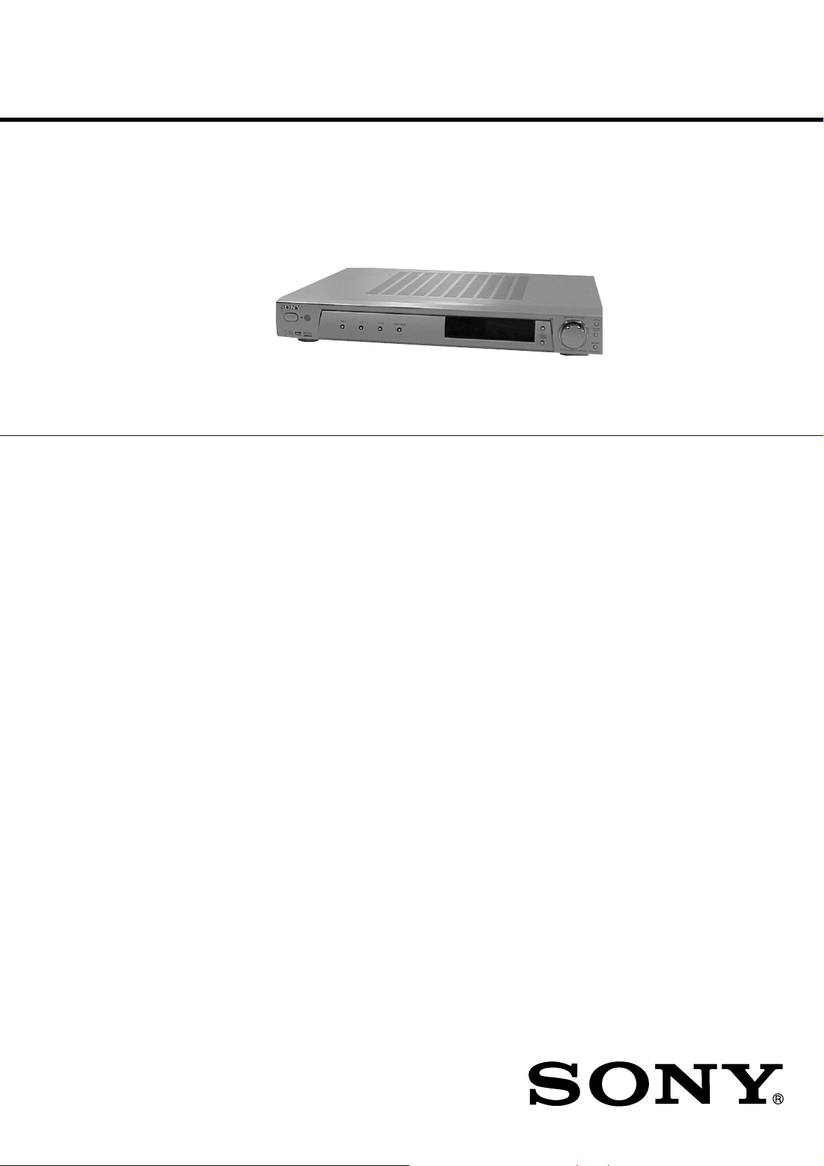
STR-KSL5
SERVICE MANUAL
Ver 1.0 2002. 07
• STR-KSL5 is the receiver section in HT-SL5.
Manufactured under license from Dolby Laboratories.
“Dolby”, “Pro Logic” and the double-D symbol are
trademarks of Dolby Laboratories.
SPECIFICATIONS
Amplifier section
POWER OUTPUT
Rated Power Output at Stereo mode
(8 ohms 1 kHz, DIN) 25 W + 25 W
Reference Power Output
(8 ohms 1 kHz, THD 10 %)
1) Depending on the sound field settings and the
source, there may be no sound output.
Frequency response
MICRO SP.: 150 Hz – 50 kHz
NORMAL SP.: 10 Hz – 50 kHz
Inputs (Analog) Sensitivity: 250 mV
2) INPUT SHORT.
3) Weighted network, input level.
Inputs (Digital)
DVD (Coaxial) Sensitivity: –
DVD, TV/SAT (Optical) Sensitivity: –
1)
Front
: 35 W/ch
1)
Center
: 35 W
1)
Surround
–3/+0.5 dB
150 Hz (6 dB/oct)
Low cut Filter ON
–3/+0.5 dB (with sound
field and tone off)
Impedance: 50 kilohms
S/N
(A, 250 mV
Impedance: 75 ohms
S/N: 100 dB
(A, 20 kHz LPF)
Impedance: –
S/N: 100 dB
(A, 20 kHz LPF)
2)
: 96 dB
: 35 W/ch
3)
)
Sampling frequency
COAX, OPT 96 kHz
Outputs
LINE (SUB WOOFER) Voltage: 2 V
Video section
Inputs
Video: 1 Vp-p, 75 ohms
Outputs
Video: 1 Vp-p, 75 ohms
FM tuner section
Tuning range 87.5 – 108.0 MHz
Antenna terminals 75 ohms, unbalanced
Intermediate frequency
Sensitivity Mono: 18.3 dBf,
Usable sensitivity 11.2 dBf, 1 µV/75 ohms
S/N Mono: 76 dB
Harmonic distortion at 1 kHz
Separation 45 dB at 1 kHz
Frequency response 30 Hz – 15 kHz
Selectivity 60 dB at 400 kHz
Impedance: 1 kilohms
10.7 MHz
Stereo: 38.3 dBf,
Stereo: 70 dB
Mono: 0.3%
Stereo: 0.5%
+0.5/–2 dB
2.2 µV/75 ohms
22.5 µV/75 ohms
AEP Model
UK Model
AM tuner section
Tuning range 531 – 1602 kHz
Antenna Loop antenna
Intermediate frequency
Usable sensitivity 50 dB/m (at 999 kHz)
S/N 54 dB (at 50 mV/m)
Harmonic distortion 0.5% (50 mV/m, 400 Hz)
Selectivity At 9 kHz: 35 dB
General
Power requirements 230 V AC, 50/60 Hz
Power consumption 110 W
Power consumption (during standby mode)
Dimensions (w/h/d) 430 × 63 × 289 mm
Mass (Approx.) 4.6 kg
Design and specifications are subject to change
without notice.
450 kHz
0.5 W
including projecting parts
and controls
9-874-108-01
2002G1600-1
© 2002.07
HOME THEATER SYSTEM
Sony Corporation
Home Audio Company
Published by Sony Engineering Corporation

STR-KSL5
Unleaded solder
Boards requiring use of unleaded solder are printed with the leadfree mark (LF) indicating the solder contains no lead.
(Caution: Some printed circuit boards may not come printed with
the lead free mark due to their particular size.)
: LEAD FREE MARK
Unleaded solder has the following characteristics.
• Unleaded solder melts at a temperature about 40°C higher than
ordinary solder.
Ordinary soldering irons can be used but the iron tip has to be
applied to the solder joint for a slightly longer time.
Soldering irons using a temperature regulator should be set to
about 350°C.
Caution: The printed pattern (copper foil) may peel away if the
heated tip is applied for too long, so be careful!
• Strong viscosity
Unleaded solder is more viscous (sticky, less prone to flow) than
ordinary solder so use caution not to let solder bridges occur such
as on IC pins, etc.
• Usable with ordinary solder
It is best to use only unleaded solder but unleaded solder may
also be added to ordinary solder.
TABLE OF CONTENTS
1. GENERAL ·········································································· 3
2. TEST MODE ······································································4
3. DIAGRAMS ········································································ 6
3-1. Block Diagrams
– Main Section – ··························································· 7
– Display/Power Section – ············································ 8
3-2. Printed Wiring Board – Digital Section – ····················· 9
3-3. Schematic Diagram – Digital Section (1/2) – ············· 10
3-4. Schematic Diagram – Digital Section (2/2) – ············· 11
3-5. Printed Wiring Board – AMP Section – ······················ 12
3-6. Schematic Diagram – AMP Section – ························· 13
3-7. Printed Wiring Board – Input Section – ······················ 14
3-8. Schematic Diagram – Input Section – ························· 15
3-9. Printed Wiring Board – Video Section – ····················· 16
3-10. Schematic Diagram – Video Section – ······················· 17
3-11. Printed Wiring Board – Display Section – ·················· 18
3-12. Schematic Diagram – Display Section – ···················· 19
3-13. Printed Wiring Board – Power Section – ···················· 20
3-14. Schematic Diagram – Power Section –······················· 21
3-15. IC Block Diagram ······················································· 22
3-16. IC Pin Function Descriptions ······································ 23
Notes on chip component replacement
•Never reuse a disconnected chip component.
• Notice that the minus side of a tantalum capacitor may be damaged
by heat.
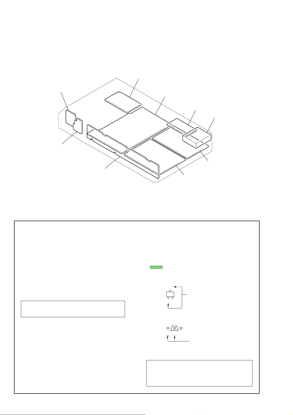
4. EXPLODED VIEWS
4-1. Front Panel Section ····················································· 27
4-2. Chassis Section ···························································· 28
5. ELECTRICAL PARTS LIST ······································· 29
SAFETY-RELATED COMPONENT WARNING!!
COMPONENTS IDENTIFIED BY MARK 0 OR DOTTED LINE WITH
MARK 0 ON THE SCHEMATIC DIAGRAMS AND IN THE PARTS
LIST ARE CRITICAL TO SAFE OPERATION. REPLACE THESE
COMPONENTS WITH SONY PARTS WHOSE PART NUMBERS
APPEAR AS SHOWN IN THIS MANUAL OR IN SUPPLEMENTS
PUBLISHED BY SONY.
2
SECTION 1
GENERAL
Parts Identification
The items are arranged in alphabetical order.
Refer to the pages indicated in parentheses ( ) for details.
Main unit
STR-KSL5
This section is extracted
from instruction manual.
1 2 3 4 5 6 7 9 q;
Display 7 (20)
DVD 4 (17)
IR receptor 2
MASTER VOLUME 9 (17)
MUTING qs (17)
PLII q; (19)
PRESET TUNING +/– 8 (24)
SOUND FIELD qa (18, 21)
TUNER 6 (17, 23, 24)
TV/SAT 5 (17)
VIDEO 3 (17)
?/1 (power) 1 (12, 16, 17, 22)
8
qs qa
3
STR-KSL5
SECTION 2
TEST MODE
FACTORY SET MODE
* All preset contents are reset to the default setting.
* Procedure:
While depressing the VIDEO and the PLII buttons
simultaneously, press the power
button to turn on the main
?/1
power. The message “FACTORY” appears and switch off the set.
Press the power
button again, and the present contents are
?/1
reset to the default values.
MICRO/NORMAL SPEAKER SELECTION MODE
* Either the micro speaker mode or normal speaker mode can be
selected.
* Procedure
While depressing the MUTING button, press the power
?/1
button to turn on the main power. Either the message “MICRO
SP.” or “NORM. SP.” appears. Select the desired mode.
SOUND FIELD CLEAR MODE
*The preset sound field is cleared when this mode is activated.
Use this mode before returning the product to clients upon
completion of repair.
* Procedure:
While depressing the SOUND FIELD button, press the power
button to turn on the main power. The message
?/1
“S. F. CLR” appears and initialization is performed.
ALL CLEAR MODE
*The all preset value is cleared when this mode is activated.
* Procedure :
While depressing the VIDEO and the SOUND FIELD buttons
simultaneously, press the power
button to turn on the main
?/1
power. The message “INITIAL” appears and clear all preset value.
FAN CONTROL MODE
* Either the fan auto mode or fan on mode can be selected.
* Procedure:
While depressing the PLII button, press the power
?/1
button.
Either the message “FAN AUTO” or “FAN ON” appears. Select
the desired mode.
SOFTWARE VERSION DISPLAY MODE
*The software version is displayed.
* Procedure:
While depressing the VIDEO and the MUTING buttons
simultaneously, press the power
button to turn on the main
?/1
power. The model name, destination and the software version are
displayed.
KEY CHECK MODE
* Button check
* Procedure:
While depressing the DVD and the MUTING buttons
simultaneously, press the power
power.
“REST 09” appears.
Every pressing of any button other than ?/1 counts down the
buttons. The buttons which are already counted once are not
counted again. When all buttons are pressed “REST 00” appears.
button to turn on the main
?/1
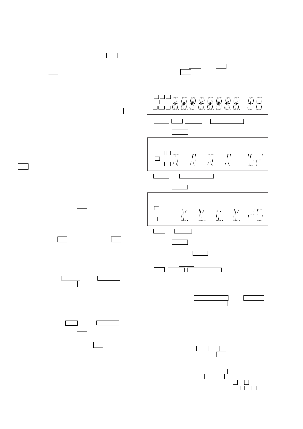
FLUORESCENT INDICATOR TUBE TEST MODE
* All fluorescent segments are tested. When this test is activated,
all segments turn on at the same time, then each segment turns on
one after another.
* Procedure:
While depressing the DVD and the PLII buttons simultaneously,
press the power
button to turn on the main power.
?/1
1. All segments turn on.
D
D
SP SP A SP B
L
C R
SW
L F E
SL SRSSB
D
DIGITAL EX PRO LOGIC II DTS-ES
OPT COAX MULTI CH IN 12
D
D.RANGE
NEO : 6 MPEG-2 AAC
dB
kHz
mft.
MHz
RDSMONOSTEREOEQ
MEMORY
SLEEP
VIDEO , DVD , TV/SAT and TUNER FM/AM LED turn on.
2. Press the VIDEO button, confirm display
SP A SP B
L
SL SR
R
EX II -ES
COAX 1
D.RANGE
NEO : 6 -2
MONOEQ
MEMORY
dB
Hz
ft.
VIDEO , and TUNER FM/AM LED turn on.
3. Press the VIDEO button, confirm display
D
D
SP
SW
SSB
D
OPT MULTI CH IN 2
C
L F E
DIGITAL PRO LOGIC DTS
D
MPEG AAC
k
m
MHz
RDSSTEREO
SLEEP
DVD and TV/SAT LED turn on.
4. Press the VIDEO button, all segments turn off.
5. Every pressing of the VIDEO button turns on each segment and
LED one after another in the same order.
(Not only the VIDEO button, but also the other buttons such as
DVD , TV/SAT , TUNER FM/AM can be used.)
TUNER CHECK MODE
*Tuner check
* Procedure :
While depressing the TUNER FM/AM and the MUTING
buttons simultaneously, press the power ?/1 button to turn on
the main power. TUN CHK appears and the tuner checking is
performed.
DSP TEST MODE
* DSP tests are performed.
* Procedure :
There are two different methods to enter the test mode.
(1) While depressing the DVD and SOUND FIELD buttons
simultaneously, press the power ?/1 button to turn on the
main power.
(2) When the set is turned on, by using the remote controller, press
Cursor button three times, then press the MAIN MENU button
one time and thenpress the MUTING button one time.
• Select the item by pressing Cursor button ( V or v ).
• Select the function by pressing Cursor button ( B or b ).
4
STR-KSL5
Items
SWAP
DSP Version
DSP communication
Bass Management
Main Speaker cut off Freq.
LFE cut off Freq.
Co-ef. Read Address
Co-ef. Read Data
Co-ef. Write Address
Co-ef. Write Data
SRAM
Total operation time
Longest Power ON time
Output time less than
–50dB volume
Output time less than
–40dB volume
Output time less than
–30dB volume
Output time less than
–20dB volume
Output time less than
–10dB volume
Output time less than
0dB volume
Protector count value
Fuse open count value
EEPROM CONDITION
EEPROM READ
EEPROM Super Reset
DSP HALT MODE
Function
NORM
ALL
C SW
SLSR
–
–
–
–
–
–
–
–
–
OFF
ON
–
–
–
–
–
–
–
–
–
–
–
–
–
–
Description
Normal channel output
Left input t Front Left, Surround Left, Center channel output
Right input t Front Right, Surround Right, Sub Woofer channel output
Left input t Center channel output
Right input t Sub Woofer channel output
Left input t Surround Left channel output
Right input t Surround Right channel output
“DSPV XXX” is displayed. Three large charactors are the dsp version that
is being used.
When this item is selected the message will be displayed “ OK ” if the
checking is correct. “ ERROR ” will be displayed in a case of an error.
Not used for service
Not used for service
Not used for service
Not used for service
Not used for service
Not used for service
Not used for service
“ RAMC. OFF ” will be displayed in a case of no checking.
By pressing Cursor button the checking starts.
“ RAMC. PASS ” will be displayed if the checking is good.
“ RAMC. NG ” will be displayed if an error occurs.
TTL-XXXX xx is displayed.
LNG-XXXX xx is displayed.
V50-XXXX xx is displayed.
V40-XXXX xx is displayed.
V30-XXXX xx is displayed.
V20-XXXX xx is displayed.
V10-XXXX xx is displayed.
V00-XXXX xx is displayed.
PROTXXXX xx is displayed.
FUSEXXXX xx is displayed.
E- XXXX is displayed.
S RST t Super Reset : first time use EEPROM or test pattern
corrupted
FAIL t EEPROM read / write with microcom has problem
V CHG t Software version change
D CHG t Destination / model change
CLEAR t Back up data initialize
NORM t Normal AC on
E- XXX-XX is displayed.
First four hex code is EEPROM address (controlled by +/– button).
Last two hex code is EEPROM data.
S.RST- XXX is displayed.
When YES is selected, press Cursor button to clear all EEPROM data
HALT NO or HALT YES is displayed.
Remark
Selection of setting
output channels
Checking communication
between DSP and microcom
Checking communication
between DSP and SRAM
Four large charactors are
hour. Two small charactors
are minutes.
0 to 255
5
STR-KSL5
r
C
B
These are omitted.
E
Q
• Circuit Boards Location
POWER SW board
IR board
SECTION 3
DIAGRAMS
STANDBY board
AMPLIFIER board
VIDEO board
FM/AM tune
INPUT board
DISPLAY board
DIGITAL board
THIS NOTE IS COMMON FOR PRINTED WIRING BOARDS AND SCHEMATIC DIAGRAMS.
(In addition to this necessary note is printed in each block.)
For schematic diagrams.
Note:
• All capacitors are in µF unless otherwise noted. p : pF. 50
WV or less are not indicated except for electrolytics and
tantalums.
• All resistors are in Ω and 1/
specified.
•%: indicates tolerance.
f
•
• 2 : nonflammable resistor.
• C : panel designation.
Note: The components identified by mark 0 or dotted line
: internal component.
with mark 0 are critical for safety.
Replace only with part number specified.
W or less unless otherwise
4
For printed wiring boards.
Note:
• X : parts extracted from the component side.
a
•
• : Pattern from the side which enables seeing.
: Through hole.
• A : B+ Line.
• B : B– Line.
•Voltages and waveforms are dc with respect to ground
under no-signal (detuned) conditions.
No mark : FM
•Voltages are taken with a VOM (Input impedance 10 MΩ).
Voltage variations may be noted due to normal production tolerances.
•Waveforms are taken with a oscilloscope.
• Circled numbers refer to waveforms.
• Signal path.
F : ANALOG
J : DIGITAL
c : DVD
6
Caution:
Pattern face side: Parts on the pattern face side seen from
(Side A) the pattern face are indicated.
Par ts face side: Parts on the parts face side seen from
(Side B) the parts face are indicated.
B
CE
These are omitted.
3-1. Block Diagrams – Main Section –
TU901
TUNER UNIT
L CH
R CH
MUTE
STEREO
L CH
R CH
MUTE
STEREO
INPUT SELECT, VOLUME CONT
SELECTOR
DVD
AUDIO
IN
TV/SAT
AUDIO
IN
VIDEO
AUDIO
IN
VIDEO
AUDIO
OUT
MONITOR
TV/SAT
OPTICAL
DVD
OPTICAL
DVD
COAX
OUT
VIDEO
IN
TV/SAT
IN
DVD
IN
VIDEO
OUT
L
R
L
R
L
R
L
R
IC301
OPTICAL
RECEIVER
IC302
OPTICAL
RECEIVER
J301
J402
J401
J251
J252
J255
J254
J253
L CH
R CH
IC201
VIDEO SWITCH
69
LIN5
76
RIN5
71
LIN7
RIN7
74
62
LIN1
59
RIN1
61
LREC1
REC1
60
1
LIN8
8
RIN8
TUNEDCEST-DI
TUNED
LATCHDIDO
IC303
11 10
IC401
ATT
ARPUT
9
BIAS
111312
4
SROUT
SWOUT
VOLUME
ALOUT
10
AMP
AMP
ST-DO
SCLK
LOUT
ROUT
COUT
SLOUT
DSLIN
DSRIN
DSWIN
LATCH
6
5
6
5
CLK
DLIN
DRIN
DCIN
DATA
DVDD
IC1502
IC1552
IC303
98
51
55
39
47
43
35
27
28
31
29
30
32
20
CLK
21
22
23
7
2
3
7
2
3
10
5231
IC1502
IC1552
1
1
29
26
22
MUTE
Q361-366
VIDEO-MUTE
VIDEO-SW2
VIDEO-SW1
X1101
12.288MHz
L-CH
R-CH
C-CH
SL-CH
SR-CH
SW-CH
DO
LATCH
76DO75
78
SLATCH
MUTE
MUTE
27
28
23
25
26
24
30
32
+3.3V
REG
Q401
MUTE
DRIVE
Q379
TUNED
STEREO
74
73
STEREO
21
22 XIN
TUNED
IC1101
DIGITAL AUDIO
I/F RECEIVER
XOUT
DIN1
4
DIN0
3
XMODE
DIN2
5
LOUT1
ROUT1
LOUT3
LOUT2
ROUT2
ROUT3
LIN+
RIN+
DI
SCLK
DO
DI
OUTPUT
CIRCUIT
INPUT
CIRCUIT
+7V
FUNCTION
MUTE SW
Q1601, 1602
14
DATA
24AUDIO
15LRCK
14BCK
13CKOUT
16DATAO
17XSATE
34ERROR
35
36
37CE
38CLK
47CKSE1
48
15
IC1501
CODEC
16
CLK
LATCH
AUDIO
LRCK
CKOUT
D1601
BCK
AUDIO
INTERFACE
24 21
ANA/DIG
BCKO
LRCK
SDTI1
SDTI2
SDTI3
SDT0
MCLK1
S.MUTE
PD
3 17
9 8
PD
SMUTE
F.MUTE
SYSTEM CONTROL
D1101
DATAO
4
5
6
7
8
9
39
CDT1
43
CCLK
42
CS
41
IC1601 (1/2)
13CS12
AUDIO
LRCK
BCK
CKOUT
10
SCL
L-CH
R-CH
C-CH
SL-CH
SR-CH
SW-CH
GP8
69
LRCKI2
28
BCKI2
29
KFSIO
22
SDI2
30
BCKO
20
LRCK
19
SDO1
23
SDO2
24
SDO3
25
SDI1
18
SCKOUT
14
EXLOCK
59 2 32 33 34 35 36 56
CDT1
IC701 FL AMP
OUT
1IN
4
IC751 FR AMP
1IN
OUT
4
IC501 C AMP
OUT
1IN
4
IC601 SL AMP
OUT
1IN
4
IC651 SR AMP
OUT
1IN
XRST
HACN
6 5 19 20 18 4 3
XRST
HACN
IC1201
AUDIO DSP
HDIN
HCLK
HDOUT
HDIN
HCLK
HDOUT
4
HCS
HCS
BST
BST
STR-KSL5
TM701
L
FRONT
TM601
CENTER
RELAY SW
Q402
17
WOOFER RELAY
R
SPEAKERS
L
REAR
R
J403
SUB
WOOFER
• Signal Path
: ANALOG
: DIGITAL
: DVD
RY70 1
RY50 1
RY60 1
PROTECT DET
Q730-732
RELAY SW
Q520, 620, 720
IC402 SW AMP
5IN
9MCLK1
X1201
13.5MHz
12MCLK2
A0-A15
A0-A15
44CSO
45WEO
GP9
PM
68
113
2
7
100
1
99
PM
GP9
DATAO
ERROR
XSTATE
98DO97
DI
17
96CE95
IC1202
SDRAM
CS
6
WE
CLK
94
93
XMODE
CKSEL1
7OUT
FAN ON/OFF DET
Q550, 551
67
72
71
70
PROTECTOR
REAR RELAY
FRONT RELAY
CENTER RELAY
RY401
64
FAN_ON
77
STR-KSL5
– Display/Power Section –
+3.3V
(STBY)
FLASH
PROGRAMMING
RV101
VOL
ENCODER
S111-115
FUKCTION
KEY
S101-104
FUKCTION
KEY
S118
POWER ON/OFF
IC102
REMOTE
CONTROL
RECEIVER
+3.3V
(STBY)
CNS3
FL101
FLUORESCENT
IC1601(2/2)
SYSTEM CONTROL
VOL(A)
1
3
60
VOL(B)
59
A/D3
41
A/D2
40
POWER KEY
56
1
2
4
5
9
10
IC101
BUFFER
1A
1B
2A
2B
3A
3B
CLK
31Y
62Y
83Y
8
DIN
7
STB
9
+5V
62CLK
61DIN
63FL_STB
48STOP
+3.3V (STBY)
SIRCS
13
X1601
16MHz
54
82 XO
83 XI
FLASH1
28
FLASH2
27
66POWER RELAY
IC1604
EEPROM
SDA
34SDA
33SCL
5
SCL
6
+3.3V
+2.5V
IC1602
RSTX
77
MD0
49
MD2
51
65FAN_CLK
68F_CTRL2
69F_CTRL1
RESET
21
+5V
AMP+V
AMP-V
AUDIO+
FAN901
Q861-865
FAN
CONTOROL
Q866
FAN
CLK
+10V (TUNER)
-27V
+7V
INDICATOR TUBE
F2
14-29 42-31
SEG1-16
FL/LED DRIVE
GRID1-12
IC152
Q901
STOP
DET
IC1904
+3.3V
REG
Q951
RELAY
DRIVE
IC1901
2
+3.3V/+2.5V
REG
5
IC1503
REG
IC1902
+10V
REG
IC403
REG
+5V
+7V
F1
F1
F2
D151-154
4VIDEO LED
3DVD LED
2TV LED
1AUX LED
D956, 957
+RECT
D952-955
13
STBY
+REC
T902
AC
IN
RY901
4
13
D809
T901
F901
+,-RECT
D810, 811
-RECT
13
D801-804
13
+,-RECT
IC405
+5V
+5V (VIDEO)
IC1903
+5V
REG
+5V
REG
13
D805-808
13
+RECT
IC404
-7V
-7V
REG
13
F1
F2
IC406
-5V
-5V (VIDEO)
REG
13
88
STR-KSL5
3-2. Printed Wiring Board – Digital Section –
IC1502
IC1501
IC1552
IC1601
IC1604
IC1602
• : Uses unleaded solder.
C1640
IC1101
IC1201
IC1202
• See page 6 for Circuit Boards Location.
TU901
TUNER
UNIT
C1227
IC1904
IC1902
C1913
C1314
C1304
C1305
IC1901
IC1503
14
• Semiconductor
Location
Ref. No. Location
D1101 B-3
D1501 B-10
D1502 B-10
D1601 E-1
D1905 F-8
D1906 F-8
D1907 E-8
14
IC1101 B-4
IC1201 C-3
IC1202 C-4
IC1501 B-2
IC1502 B-1
IC1503 C-10
IC1552 C-1
IC1601 E-2
IC1602 F-2
IC1604 F-2
IC1901 F-8
IC1902 F-7
IC1903 F-9
IC1904 E-7
Q1601 E-1
Q1602 E-1
C1914
IC1903
12
18
1
7
99
STR-KSL5
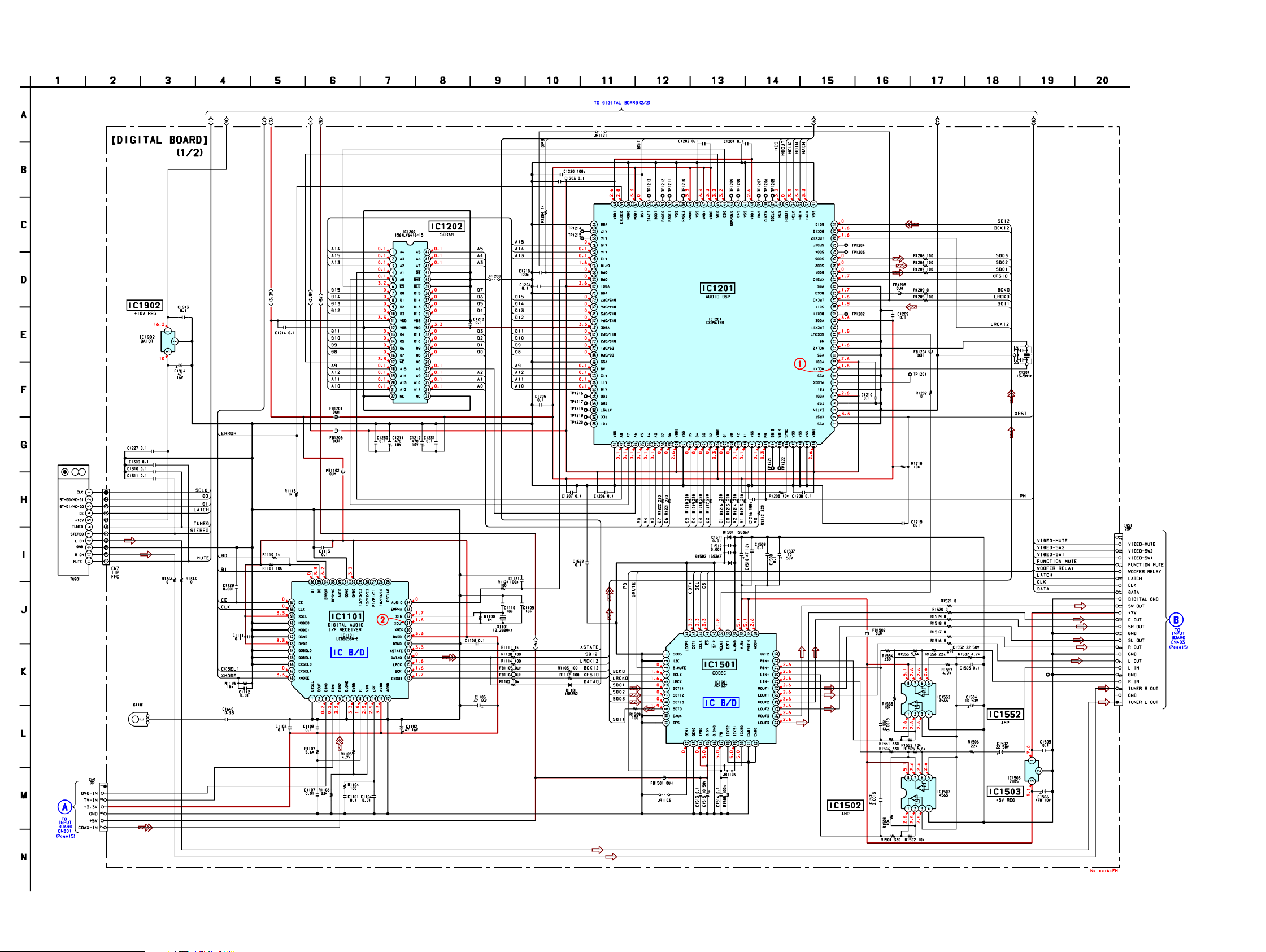
3-3. Schematic Diagram – Digital Section (1/2) –
• See page 11 for Wavefoms. • See page 22 for IC Block Diagrams. • See page 23 for IC Pin Function Description.
1010
STR-KSL5
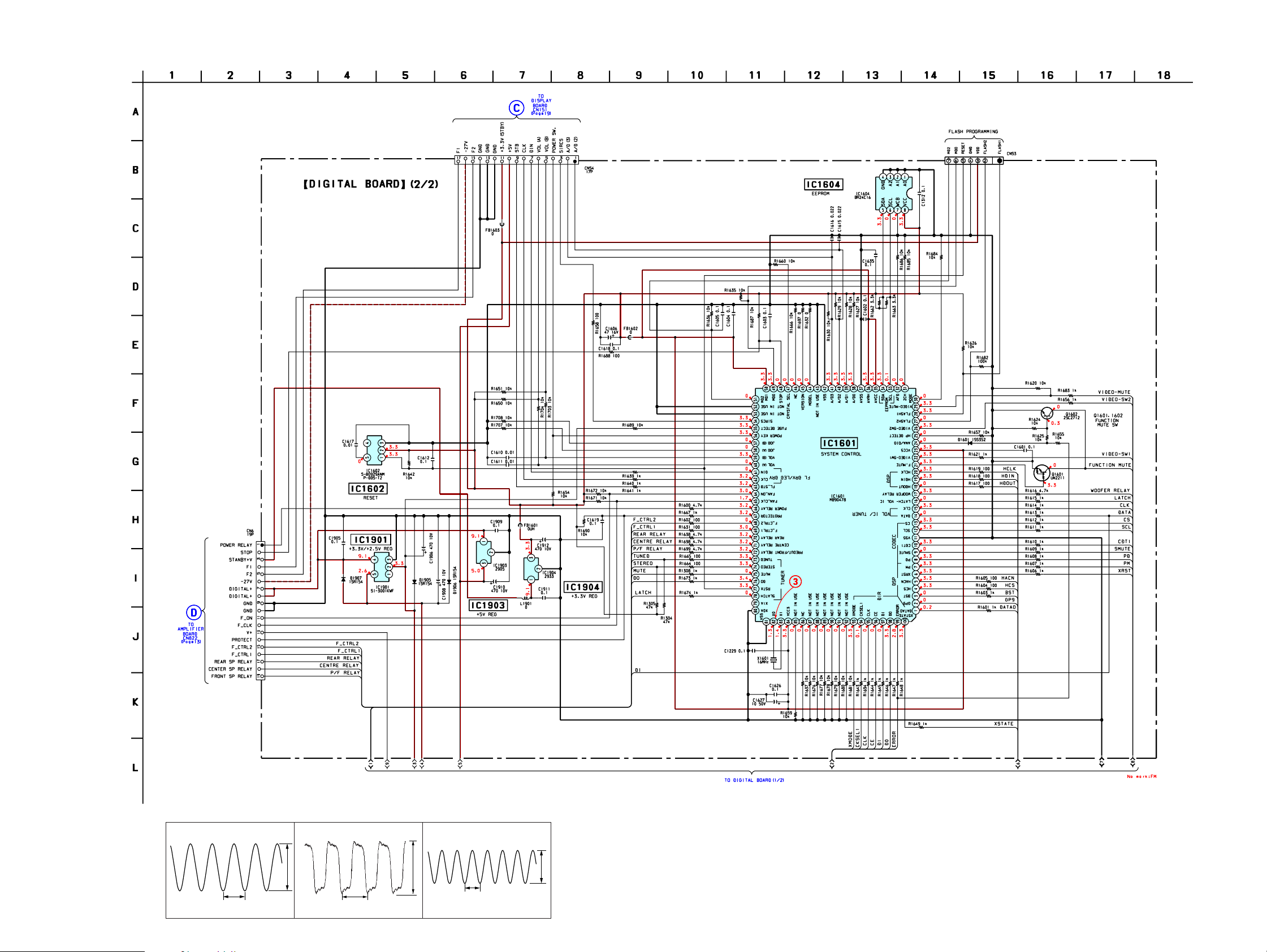
3-4. Schematic Diagram – Digital Section (2/2) –
• See page 25 for IC Pin Function Description.
• Waveforms
– DIGITAL Board –
1
IC1201 9 (MCLK1)
40ns/div 1V/div 40ns/div 1V/div 40ns/div 1V/div
74 nsec
3.6 Vp-p
2
IC1101 wa (XOUT)
81.3 nsec
4.2 Vp-p
3
IC1601 is (XO)
62.5 nsec
2.9 Vp-p
1111
STR-KSL5
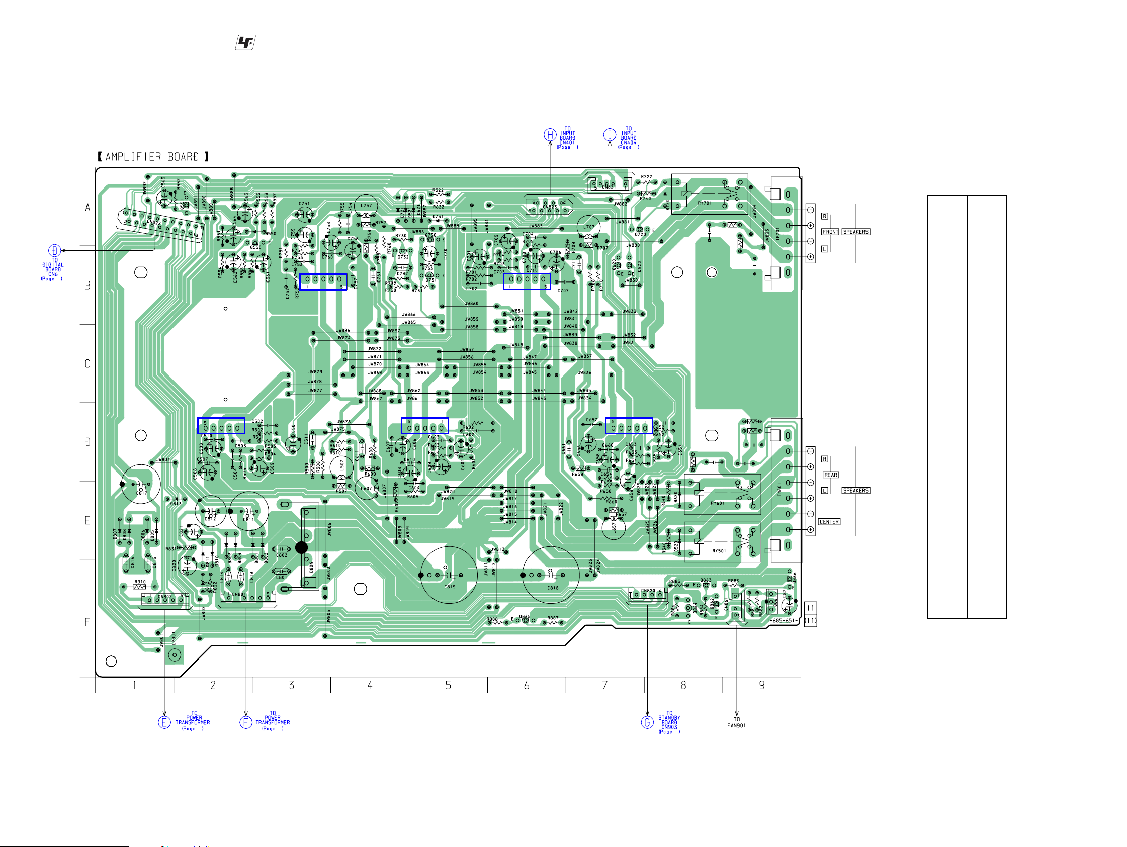
3-5. Printed Wiring Board – AMP Section –
9
IC501 IC601
• : Uses unleaded solder.
IC751
• See page 6 for Circuit Boards Location.
IC701
14 14
IC651
R643
C643
C791
R791
R741
C642
R642
R641
C641
C741
• Semiconductor
Location
Ref. No. Location
D520 E-8
D521 A-5
D550 A-2
D620 E-8
D621 A-5
D720 A-8
D721 A-2
D731 A-5
D801 E-3
D802 E-3
D803 E-2
D804 E-2
D805 E-1
D806 E-1
D807 E-1
D808 E-1
D809 F-3
D810 E-2
D811 E-2
D812 F-2
D813 E-2
IC501 D-2
IC601 D-5
IC651 D-7
IC701 B-6
IC751 B-3
20 20
Q520 B-7
Q550 B-2
Q551 A-2
Q620 B-7
Q720 A-7
Q730 B-5
Q731 B-5
Q732 B-4
Q861 F-9
Q862 F-8
Q863 F-8
Q864 F-8
Q865 F-6
Q866 F-9
20
1212
 Loading...