

Sony STRK-650-P Service manual
STR-K650P
SERVICE MANUAL
Ver 1.0 2003. 04
• STR-K650P is the tuner and the amplifier
section in HT-DDW650.
Dolby Laboratories Licensing Corporation.
“DOLBY” the double-D symbol ; “AC-3” and “PRO LOGIC”
are trademarks of Dolby Laboratories Licensing Corporation.
SPECIFICATIONS
POWER OUTPUT AND TOTAL
HARMONIC DISTORTION:
With 8 ohm loads, both channels driven, from
40 – 20,000 Hz; rated 70 watts per channel
minimum RMS power, with no more than
0.7 % total harmonic distortion from 250
milliwatts to rated output (Models of area code
U only).
Amplifier section
POWER OUTPUT
Rated Power Output at Stereo Mode
(8 ohms 40 Hz – 20 kHz, THD 0.7 %)
70 W + 70 W
Reference Power Output
(8 ohms 1 kHz, THD 0.7 %)
1)
:80 W/ch
FRONT
1)
CENTER
SURR
1) Depending on the sound field settings and the
Frequency response
CD, MD/TAPE, DVD,
VIDEO 1, 2
: 80 W
1)
: 80 W/ch
source, there may be no sound output.
10 Hz – 50 kHz
+0.5/–2 dB (with sound
field and tone bypassed)
Inputs (Analog)
CD, MD/TAPE, DVD,
VIDEO 1, 2
2) INPUT SHORT (with sound field and tone
3) Weighted network, input level.
Inputs (Digital)
DVD (Coaxial)
VIDEO 2 (Optical)
Outputs
MD/TAPE (OUT),
VIDEO 1
(AUDIO OUT)
SUB WOOFER
Tone
Gain levels: ±6 dB, 1 dB step
bypassed).
Sensitivity: 500 mV
Impedance: 50 kilohms
2)
S/N
: 96 dB
(A, 500 mV
Sensitivity: –
Impedance: 75 ohms
S/N: 100 dB
(A, 20 kHz LPF)
Sensitivity: –
Impedance: –
S/N: 100 dB
(A, 20 kHz LPF)
Voltage: 500 mV
Impedance: 10 kilohms
Voltage: 2 V
Impedance: 1 kilohms
3)
)
US Model
9-877-334-01
2003D167800-1
© 2003.04
— Continued on next page —
FM STEREO FM-AM RECEIVER
Sony Corporation
Home Audio Company
Published by Sony Engineering Corporation

STR-K650P
FM tuner section
Tuning range 87.5 - 108.0 MHz
Antenna terminals 75 ohms, unbalanced
Intermediate Frequency
Sensitivity
Mono: 18.3 dBf, 2.2 µV/75 ohms
Stereo:
Usable sensitivity 11.2 dBf, 1 µV/75 ohms
S/N
Mono: 76 dB
Stereo: 70 dB
Harmonic distortion at 1 kHz
Mono: 0.3%
Stereo: 0.5%
Separation 45 dB at 1 kHz
Frequency response 30 Hz – 15 kHz,
Selectivity 60 dB at 400 kHz
10.7 MHz
38.3 dBf, 22.5 µV/75 ohms
+0.5/–2 dB
AM tuner section
Tuning range
With 10-kHz tuning scale: 530 – 1710 kHz
With 9-kHz tuning scale: 531 – 1710 kHz
Antenna Loop antenna
Intermediate Frequency
Usable sensitivity 50 dB/m (at 1,000 kHz or
450 kHz
999 kHz)
4)
4)
S/N 54 dB (at 50 mV/m)
Harmonic distortion 0.5 % (50 mV/m, 400 Hz)
Selectivity
At 9 kHz: 35 dB
At 10 kHz: 40 dB
4) You can change the AM tuning scale to 9 kHz or
10 kHz. After tuning in any AM station, turn off
the receiver. Hold down PRESET TUNING + and
press ?/1. All preset stations will be erased when
you change the tuning scale. To reset the scale to
10 kHz (or 9 kHz), repeat the procedure.
Video section
Inputs
Video: 1 Vp-p, 75 ohms
Outputs
Video: 1 Vp-p, 75 ohms
General
Power requirements
Power consumption
Power consumption (during standby mode)
0.3 W
Dimensions 430 × 145 × 298 mm
Mass (Approx.) 7.2 kg (15 lb 14 oz)
120 V AC, 60 Hz
175 W
(16 7/8 × 5 6/8 × 11 6/8
inches) including
projecting parts and
controls
Design and specifications are subject to change without notice.
2
STR-K650P
SAFETY CHECK-OUT
After correcting the original service problem, perform the
following safety checks before releasing the set to the customer:
Check the antenna terminals, metal trim, “metallized” knobs, screws,
and all other exposed metal parts for AC leakage. Check leakage as
described below.
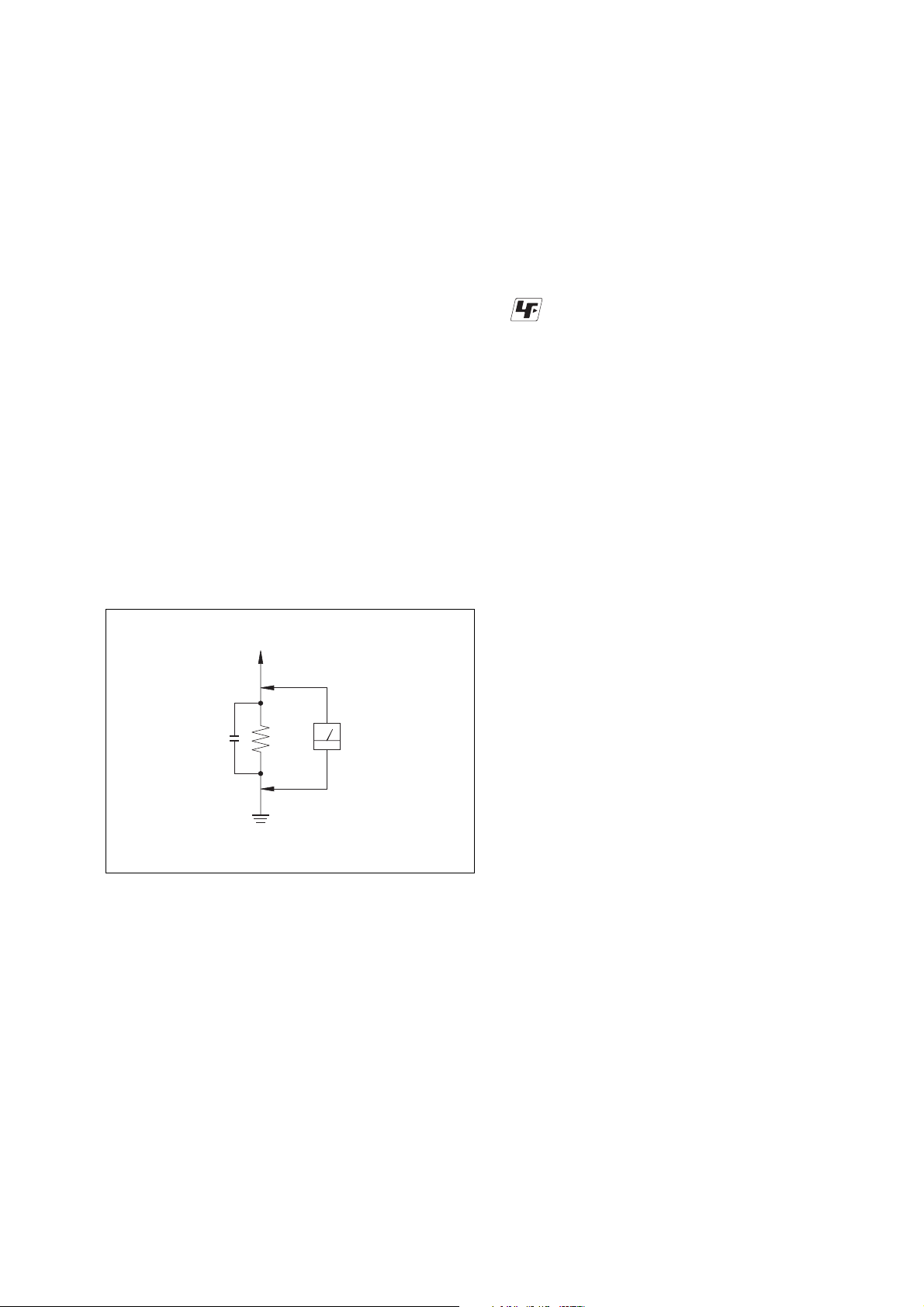
LEAKAGE
The AC leakage from any exposed metal part to earth ground
and from all exposed metal parts to any exposed metal part having
a return to chassis, must not exceed 0.5 mA (500 microamperes).
Leakage current can be measured by any one of three methods.
1. A commercial leakage tester, such as the Simpson 229 or RCA
WT-540A. Follow the manufacturers’ instructions to use these
instruments.
2. A battery-operated AC milliammeter. The Data Precision 245
digital multimeter is suitable for this job.
3. Measuring the voltage drop across a resistor by means of a
VOM or battery-operated AC voltmeter. The “limit” indication
is 0.75 V, so analog meters must have an accurate low-voltage
scale. The Simpson 250 and Sanwa SH-63Trd are examples of
a passive VOM that is suitable. Nearly all battery operated
digital multimeters that have a 2V AC range are suitable. (See
Fig. A)
Notes on chip component replacement
• Never reuse a disconnected chip component.
• Notice that the minus side of a tantalum capacitor may be
damaged by heat.
Unleaded solder
Boards requiring use of unleaded solder are printed with the leadfree mark (LF) indicating the solder contains no lead.
(Caution: Some printed circuit boards may not come printed with
the lead free mark due to their particular size.)
: LEAD FREE MARK
Unleaded solder has the following characteristics.
• Unleaded solder melts at a temperature about 40°C higher than
ordinary solder.
Ordinary soldering irons can be used but the iron tip has to be
applied to the solder joint for a slightly longer time.
Soldering irons using a temperature regulator should be set to
about 350°C.
Caution: The printed pattern (copper foil) may peel away if the
heated tip is applied for too long, so be careful!
• Strong viscosity
Unleaded solder is more viscous (sticky, less prone to flow) than
ordinary solder so use caution not to let solder bridges occur such
as on IC pins, etc.
• Usable with ordinary solder
It is best to use only unleaded solder but unleaded solder may
also be added to ordinary solder.
To Exposed Metal
Parts on Set
AC
0.15 µF
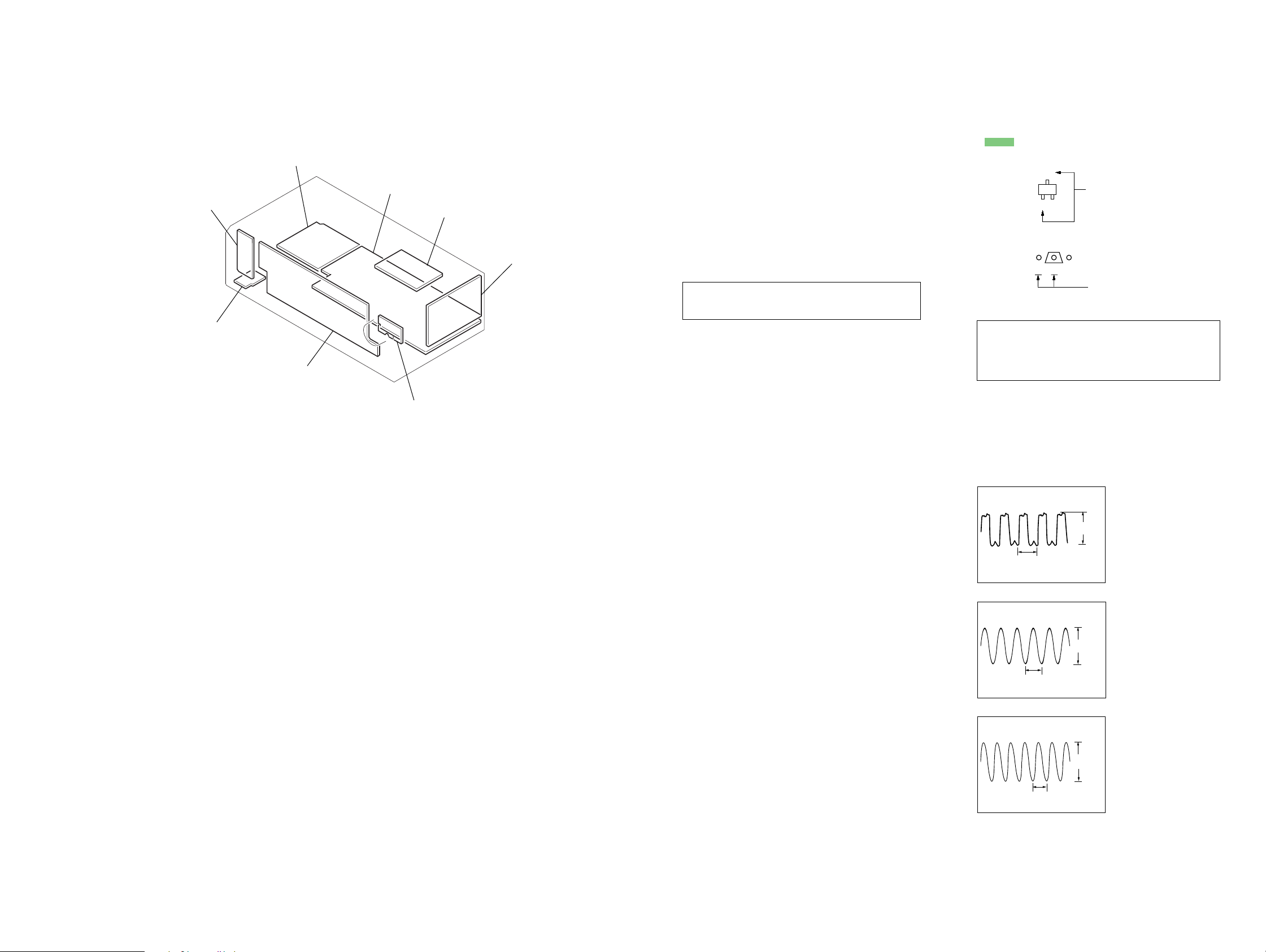
Fig. A. Using an AC voltmeter to check AC leakage.
1.5 kΩ
Earth Ground
Voltmeter
(0.75 V)
SAFETY-RELATED COMPONENT WARNING!!
COMPONENTS IDENTIFIED BY MARK 0 OR DOTTED LINE WITH
MARK 0 ON THE SCHEMATIC DIAGRAMS AND IN THE PARTS
LIST ARE CRITICAL TO SAFE OPERATION. REPLACE THESE
COMPONENTS WITH SONY PARTS WHOSE PART NUMBERS
APPEAR AS SHOWN IN THIS MANUAL OR IN SUPPLEMENTS
PUBLISHED BY SONY.
3

STR-K650P
TABLE OF CONTENTS
1. GENERAL ·········································································· 5
2. TEST MODE ······································································ 6
3. DIAGRAMS ········································································ 7
3-1. Circuit Board Location················································· 7
3-2. Block Diagrams – MAIN Section – ·····························8
– DISPLAY/POWER Section – ··································· 9
3-3. Printed Wiring Board – DIGITAL Board (SIDE A) – 10
3-4. Printed Wiring Board – DIGITAL Board (SIDE B) – 11
3-5. Schematic Diagram – DIGITAL Section (1/2) – ······· 12
3-6. Schematic Diagram – DIGITAL Section (2/2) – ······· 13
3-7. Printed Wiring Board – MAIN Board – ····················· 14
3-8. Schematic Diagram – MAIN Section (1/3) –············· 15
3-9. Schematic Diagram – MAIN Section (2/3) –············· 16
3-10. Schematic Diagram – MAIN Section (3/3) –············· 17
3-11. Printed Wiring Board – POWER Section – ··············· 18
3-12. Printed Wiring Board – DISPLAY Board – ··············· 19
3-13. Schematic Diagram – DISPLAY Section – ················ 20
3-14. Printed Wiring Board – VIDEO Section – ················· 21
3-15. Schematic Diagram – VIDEO Board – ······················22
3-16. IC Block Diagrams····················································· 23
3-17. IC Pin Function Descriptions ····································· 25
4. EXPLODED VIEWS ······················································ 27
4-1. Front Panel Section ····················································· 27
4-2. Chassis Section ··························································· 28
5. ELECTRICAL PARTS LIST ·······································29
4
SECTION 1
GENERAL
STR-K650P
This section is extracted
from instruction manual.
ALPHABETICAL ORDER
A – L
A. F. D. (button/indicator) w;
(22– 24)
CD 9 (20)
DIMMER 3 (21)
DISPLAY 2 (21, 31, 46)
Display qa (21)
DVD 7 (20)
ENTER qg (33, 35)
FM MODE wf (29)
INPUT MODE qd (20)
IR (receptor) 4 (36, 46)
2
314 56789q;qa qs
M – O
MAIN MENU qf (15, 26, 27, 33,
34, 51)
MASTER VOLUME qs (18, 20,
44)
MD/TAPE 8 (20)
MEMORY wg (28, 30)
MENU +/– qh (15, 26, 27, 33, 34,
51)
MENU </> qj (15, 26, 27, 33, 34,
51)
MOVIE (button/indicator) ql (23,
45)
MUSIC (button/indicator) qk (23,
24, 45)
P – Z
PHONES (jack) wh (20, 25, 45)
PRESET TUNING +/– ws (30, 48)
TUNER FM/AM q; (20, 29, 30,
33)
TUNING +/– wd (29)
VIDEO 1 5 (20)
VIDEO 2 6 (20)
NUMBERS AND SYMBOLS
2CH (button/indicator) wa1 (22, 24,
27)
?/1 (power) (14, 19, 27, 28,
35, 48)
qfqgqhqjqkqlw;wawswdwfwgwh
qd
5
STR-K650P
SECTION 2
TEST MODE
FACTORY PRESET MODE
* All preset contents are reset to the default setting.
* Procedure:
While depressing the FM MODE and the PRESET TUNING−
buttons simultaneously, press the
button again. The message
?/1
“FACTORY” appears and the present contents are reset to the
default values.
AM CHANNEL STEP 9 KHZ/10 KHZ
SELECTION MODE
* Either the 9 kHz step or 10 kHz step can be selected for the AM
channel step.
* Procedure:
Set the FUNCTION to AM. Turn off the main power.
While depressing the TUNING+ button or the
PRESET TUNING + button, press the
button to turn on
?/1
the main power. Either the message “9 k STEP” or “10 k STEP”
appears. Select the desired step.
SPEAKER SIZE SELECTION MODE
*Either Normal Speaker or Micro Satellite Speaker can be selected.
*Procedure:
While depressing the MAIN MENU button, press the
?/1
button
to turn the main power.
Either the message “NORM. SP.” or “MICRO SP.” is displayed.
Select the desired speaker size.
FLUORESCENT INDICATOR TUBE TEST MODE
* All fluorescent segments are tested. When this test is activated,
all segments turn on at the same time, then each segment turns on
one after another.
* Procedure:
While depressing the FM MODE and the MD/TAPE buttons
simultaneously, press the
1. All segments turn on.
button to turn on the main power.
?/1
4. Press the VIDEO1 button, All segments and all LEDS turn off.
5. Every pressing of the VIDEO1 button turns on each segment
and LED one after another in the same order.
(Not only the VIDEO1 button, but also the other buttons such
as VIDEO2 , DVD , MD/TAPE , CD and TUNER FM/AM can
be used.)
SOUND FIELD CLEAR MODE
*The preset sound field is cleared when this mode is activated.
Use this mode before returning the product to clients upon
completion of repair.
* Procedure:
While depressing the 2CH button, press the
button to turn
?/1
on the main power.
The message “SF. CLR.” appears and initialization is performed.
SOFTWARE VERSION DISPLAY MODE
*The software version is displayed.
* Procedure:
While depressing the FM MODE and the DVD buttons
simultaneously, press the
button to turn on the main power.
?/1
The model name, destination and the software version are
displayed.
KEY CHECK MODE
* Button check
* Procedure:
While depressing the MUSIC and the TUNING− buttons
simultaneously, press the power
power.
“REST 25” appears.
Every pressing of any button other than ?/1 counts down the
buttons. The buttons which are already counted once are not
counted again. When all buttons are pressed “REST 00” appears.
button to turn on the main
?/1
D
D
D
PROLOGIC II DTS-ESNEO : 6SPBSPASP MPEG-2 AAC
EQD.RANGE
STEREO MONO RDS
dB
kHz
mft.
MHz
LSLCR
L F E
SW
SSB SR
D
DIGITALEX
OPT COAX MULTI CH IN 12
2CH , A. F. D , MOVIE and MUSIC LED turn on.
2. Press the VIDEO button, confirm display.
L
SLRSR
EX
COAX 1
II -ES NEO : 6SPBSPA -2
EQD.RANGE
MONO
dB
2CH and MOVIE LED turn on.
3. Press the VIDEO button, confirm display
D
D
D
D
PROLOGIC DTSSP
MULTI CH IN 2
MPEG
STEREO RDS
k
m
MHz
SW
SSB
C
L F E
OPT
DIGITAL
A. F. D and MUSIC LED turn on.
Hz
ft.
AAC
MEMORY
SLEEP
MEMORY
SLEEP
COMMAND MODE SELECTION MODE
* The command mode (AV1 or AV2) of the remote commander can
be selected.
* Procedure:
1. While depressing the ENTER button, press the ?/1 button to
turn on the main power.
2. The message “C.MODE.AV 1” or “C.MODE.AV 2” appears
for a moment. Select the desired mode.
6
SECTION 3
d
DIAGRAMS
STR-K650P
3-1. Circuit Board Location
POWER board
HEADPHONE board
STANDBY board
DISPLAY board
MAIN board
VOLUME board
VIDEO board
DIGITAL boar
THIS NOTE IS COMMON FOR PRINTED WIRING
BOARDS AND SCHEMATIC DIAGRAMS.
(In addition to this necessary note is printed in each
block.)
For schematic diagrams.
Note:
• All capacitors are in µF unless otherwise noted. p : pF. 50
WV or less are not indicated except for electrolytics and
tantalums.
• All resistors are in Ω and 1/
specified.
•%: indicates tolerance.
f
•
• 2 : nonflammable resistor.
• 5 : fusible resistor.
• C : panel designation.
Note: The components identified by mark 0 or dotted line
• A : B+ Line.
• B : B– Line.
•Voltages and waveforms are dc with respect to ground
•Voltages are taken with a V OM (Input impedance 10 MΩ).
•Waveforms are taken with a oscilloscope.
• Circled numbers refer to waveforms.
• Signal path.
: internal component.
with mark 0 are critical for safety.
Replace only with part number specified.
under no-signal (detuned) conditions.
No mark : FM
Voltage variations may be noted due to normal production tolerances.
F : FM
J : CD (ANALOG)
c : DVD (DIGITAL)
W or less unless otherwise
4
For printed wiring boards.
Note:
• X : parts extracted from the component side.
a
•
•
• : Pattern from the side which enables seeing.
: Through hole.
f
: internal component.
C
These are omitted.
B
B
Q
E
CE
These are omitted.
Caution:
Pattern face side: Parts on the pattern face side seen from
(Side A) the pattern face are indicated.
Parts face side: Parts on the par ts face side seen from
(Side B) the parts face are indicated.
• Wavef orm
DIGITAL Board
1 IC1101 wa (XOUT)
4.4Vp-p
81.4ns
(12.288MHz)
2 IC1201 9 (MCLK1)
73.6ns (13.59MHz)
3 IC1601 id (XI)
62.5ns (16MHz)
1V/div, 40ns/DIV
3.7Vp-p
1V/div, 40ns/DIV
3.5Vp-p
1V/div, 40ns/DIV
77
STR-K650P
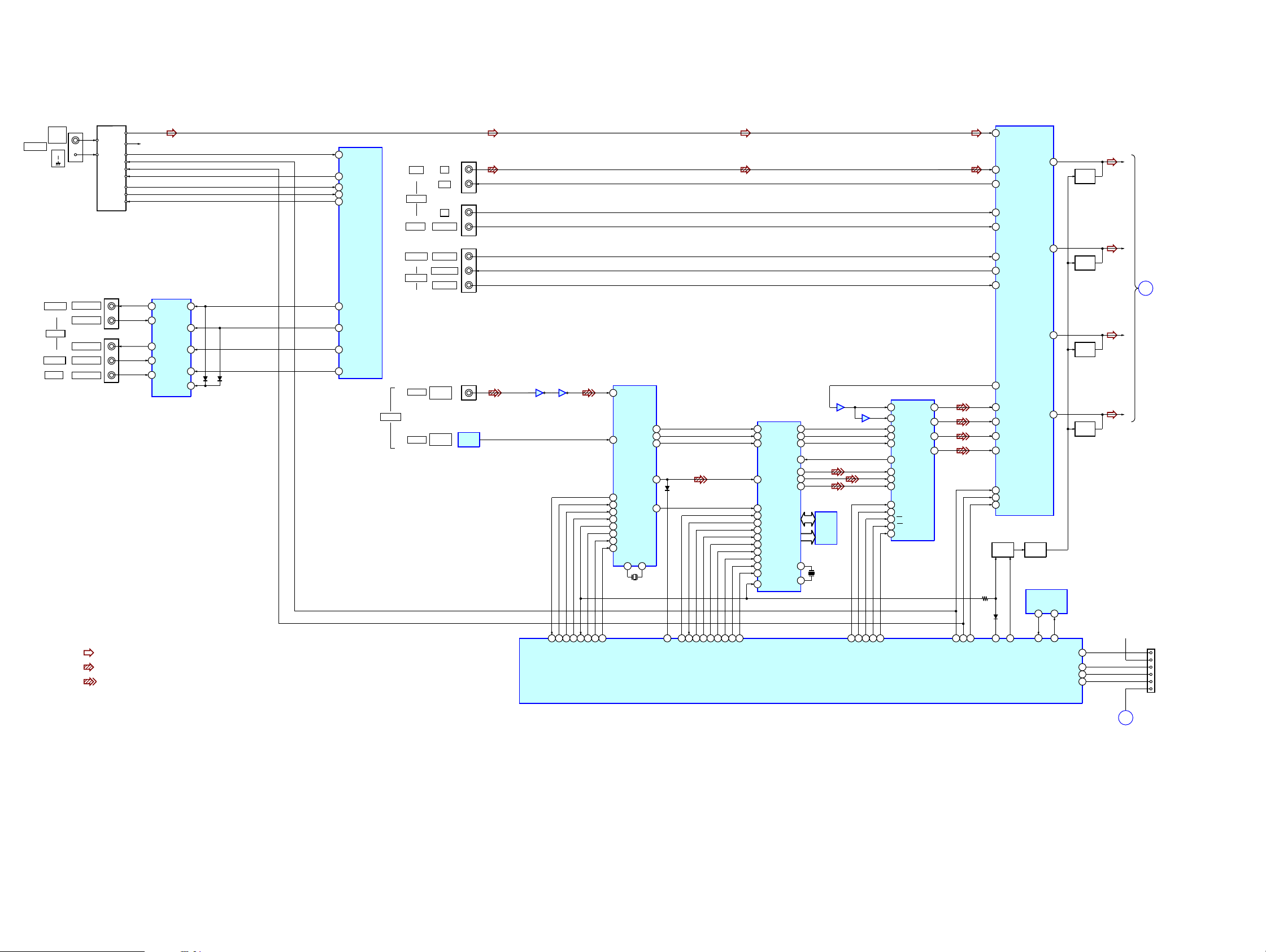
3-2. Block Diagrams – MAIN Section –
TUNER PACK
L CH
FM
R CH
ST-DO
AM
ST-DI
CLK
CE
STEREO
TUNED
MUTING
J201
VIDEO OUT
VIDEO IN
J200
VIDEO OUT
VIDEO IN
VIDEO IN
• R-CH is omitted due to same as L-CH.
• Signal Path
: FM
: CD(ANALOG INPUT)
: DVD (DIGITAL INPUT)
R-CH
1
M.OUT
13
V1
15
V1 OUT
5
V2
3
DVD
IC103
VIDEO SELECT
SW1
SW2
SW3
SW4
SW5
14
10
4
6
2
D203
ANTENNA
FM
75 Ω
COAXIAL
AM
MONITOR
VIDEO 1
VIDEO 2
DVD
D204
IC1601(1/3)
SYSTEM CONTROL.
76
DO
78
SLATCH
74
STEREO
73
TUNED
75
MUTING
90
SW1
89
SW2
88
SW3
87
SW4
DIGITAL
CD
MD/TAPE
DVD
VIDEO 2
VIDEO 1
COAXIAL
OPTICAL
IN
OUT
IN
AUDIO IN
AUDIO IN
AUDIO OUT
AUDIO IN
DVD
IN
VIDEO 2
IN
J402
J403
J404
J1101
IC1105
OPTICAL
IN
93
XSTATE
XMODE
CKSEL1
DIGITAL AUDIO
5
DIN2
4
DIN1
35
DO
36
DI
38
CLK
37
CE
34
ERROR
17
XSTATE
48
XMODE
47
CKSEL1
IC1102
IC1102
35
62
98 97 95 96 99 100 94 1
DI
CE
DO
CLK
ERROR
IC1101
I/F RECEIVER
CK OUT
XIN XOUT
22 21
X1101
12.288MHz
LRCK
DATAO
IC201
ANALOG SOUND
PROCESSOR
4
INL1
+3.3V
L
SL
SL
C
SW
FLASH 1
FLASH 2
RESET
A
CNS3
MD0
VDD
FOR
MD2
FLASH
PROGRAMMING
L OUT
SL OUT
SW OUT
Q379
MUTING
SWITCH
SDA SCL
34 33
C OUT
IC1604
EEPROM
5 6
SDA
54
Q361
MUTING
41
Q365
MUTING
36
Q363
MUTING
35
Q364
MUTING
SCL
49MD0
MD2
51
FLASH 1
28
FLASH 2
27
80
INL3
60
RECL2
78
INL4
76
INL5
74
INL6
58
RECL1
72
INL7
14
IC1501
SMUTE
29
30
39
4
5
9
6
7
8
43
42
41
17
3
AUDIO CODEC
LIN-
LIN+
MCLKI
BCLK
LRCK
SDTO
SDTI1
SDTI2
SDTI3
CDT1
CCLK
CS
PD
S.MUTE
L OUT1
L OUT2
L OUT3
R OUT3
27
25
23
24
(ANALOG SIGNAL)
15
14
CLK
DATA
IC1502
67
-
IC1201
AUDIO DSP
22
SCK OUT
13
BCK
14
15
16
D1101
24AUDIO
20
4
5
19
HD OUT
HD IN
HCLK
7PM3
HCS
HACN
DATA0
2
18
GP9
KFSI0
29
BCKI2
28
LRCKI2
30
SDI2
69
GP8
68
GP9
35
HD OUT
33
HD IN
34
HCLK
36
HCS
32
HACN
PM
113
56
BST
2
XRST
59
EXLOCK
6
BST
XRST
14
BCKO
20
19LRCKO
18SDI1
SDO1
23
SDO2
24
SDO3
25
MCLK1
9
MCLK2
12
IC1601(2/3)
SYSTEM CONTROL
IC1202
SRAM
X1201
13.59MHz
IC1502
21
10
12
SCL
CDT1
-
13CS8PD9
BAL L+
20
LIN2
23
SLIN2
24
CIN2
25
SWIN2
28
DATA
27
CLK
29
LATCH
Q1601,1602
MUTING
CONT
D1601
16
24
21
LATCH
ANA/DIG
F.MUTING
B
88
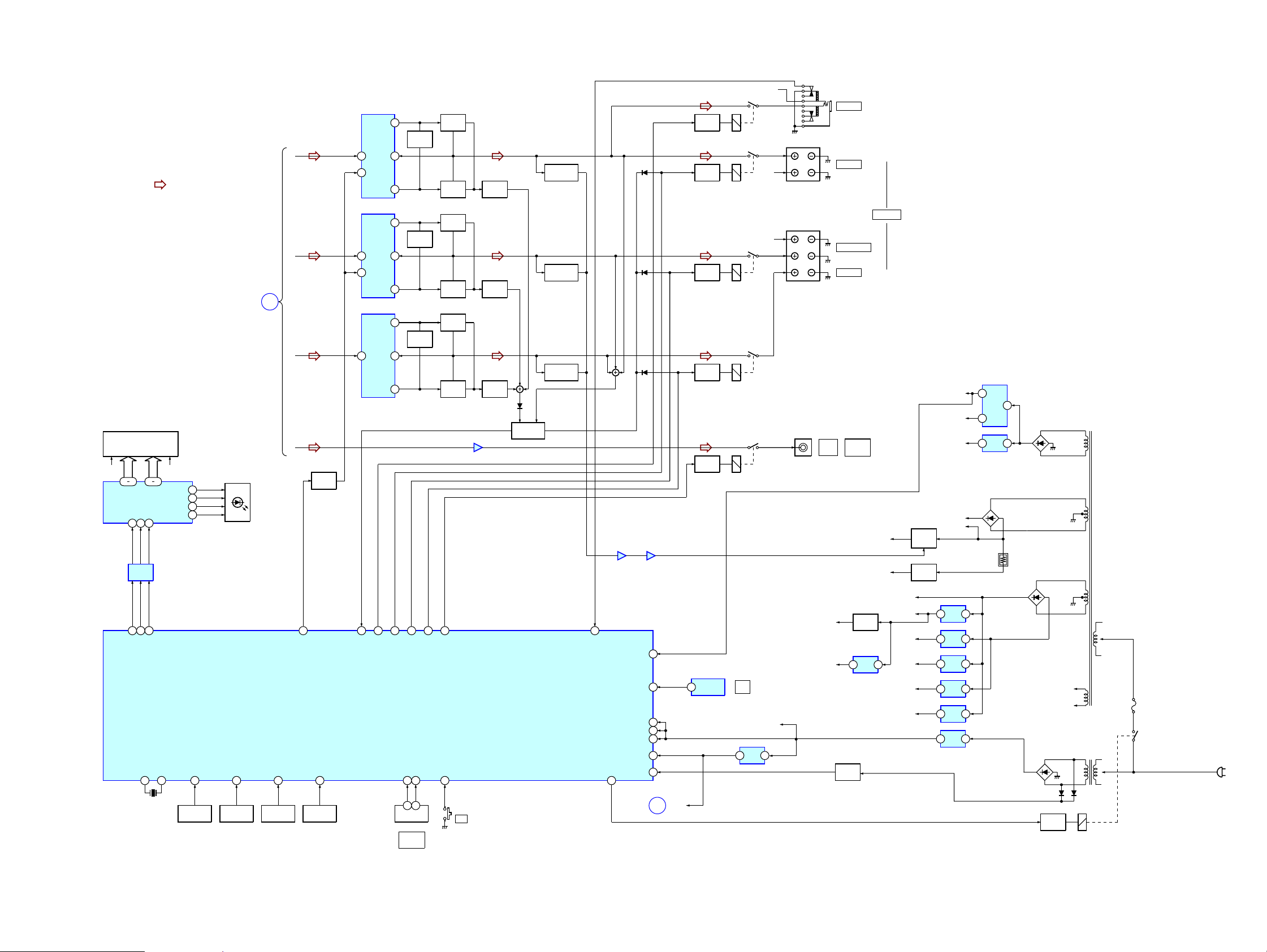
– DISPLAY/POWER Section –
STR-K650P
• R-CH is omitted due to same as L-CH
• Signal Path
FL101
FLUORESCENT
INDICATOR TUBE
F1 F2
14 29
42 31
SEG1-16
GRID1-12
DIN8CLK9STB
7
IC101
BUFFER
61
62
63
DIN
CLK
FL_STB
X0
82 83
X1601
16MHz
R-CH
IC701
POWER AMP
+V OUT2
12
Q701,702
LIMITER
L
: FM
SLSL
A
C
SW
IC100
FL DRIVE
SW1
1
SW2
2
SW3
3
SW4
4
X1
38
FUNCTION
KEY
A/D0
D102-105
39
FUNCTION
KEY
S110-115S100-106
A/D1
40
FUNCTION
KEY
S120-125
A/D2
22
AC MUTING
FUNCTION
S130-135
Q747,748
POWER
MUTING
A/D3
41
KEY
8
NF2
IN2
1
MUTING
-V OUT2
IC702
POWER AMP
+V OUT2
NF2
IN2
8
1
MUTING
-V OUT2
POWER AMP
IC501
+V OUT
1
IN+
66
67
PROTECTOR
HEADPHONE RELAY
SYSTEM CONTROL
IC1601(3/3)
9
11
12
9
11
6
IN-
2
5-V OUT
71
PREOUT/FRONT RELAY
3 1
ENCODER
RV102
MASTER
VOLUME
Q651,652
LIMITER
Q501,502
LIMITER
69
VOL(B)59VOL(A)
60
70
REAR RELAY
CENTER RELAY
Q703
BOOSTER
Q704
BOOSTER
Q653
BOOSTER
Q654
BOOSTER
Q503
BOOSTER
Q504
BOOSTER
68
WOOFER RELAY
POWER KEY
56
S152
?/1
IC601
21
FUSE DETECT
POWER RELAY
65
D731
D733
D734
IC601
57
SIRCS
AVCC
VCC3
VCC5
RSTX
STOP
55
54
35
84
23
77
48
B
1
RESET
Q740
AF POWER
PROTECT
SWITCH
PROTECT
Q640
AF POWER
PROTECT
Q540
AF POWER
PROTECT
25
HP DETECT
Q705,706
CURRENT
DETECT
Q655,656
CURRENT
DETECT
Q505,506
CURRENT
DETECT
D721
Q722,723,725
IC401
7
5
Q790
RELAY
DRIVE
Q710
RELAY
DRIVE
Q610
RELAY
DRIVE
Q550
RELAY
DRIVE
Q560
RELAY
DRIVE
IC102
REMOTE
CONTROL
RECEIVER
RY791
RY701
RY601
RY501
RY560
g
+3.3V(STBY)
IC1602
RESET
1 2
R-CH
R-CH
TM602
L
R
TM601
SR
SL
C
J405
AUDIO
OUT
+3.3V
AUDIO
+5V
J791
PHONES
FRONT
SURROUND
CENTER
SUB
WOOFER
+3.3V REG
3 1
Q921
AC DET
POWER AMP
Q471
IC1503
+5V
REG
SPEAKERS
-B
FL101
-30V
RELAY
+B
AUDIO
+7V
AUDIO
-7V
VIDEO
+5V
VIDEO
-5V
TUNER
+10V
Q691,692
-B
SWITCH
Q801
-30V REG
+3.3V
+2.5V
+5V
IC801
+7V
1 3
REG
IC802
-7V
3 2
REG
IC807
+5V
3 1
REG
IC804
-5V
3 2
REG
IC1902
+10V
3 1
REG
IC1904
+3.3V
3 1
REG
IC1901
+3.3V
2
REG
4
+2.5V
5
REG
IC1903
+5V
3 1
REG
D802
+B
-B
D820-823
D902-905
D910-913
D914
Q901
RELAY
DRIVE
T901
F1
F2
D915
RY901
T902
F901
AC
IN
99
STR-K650P
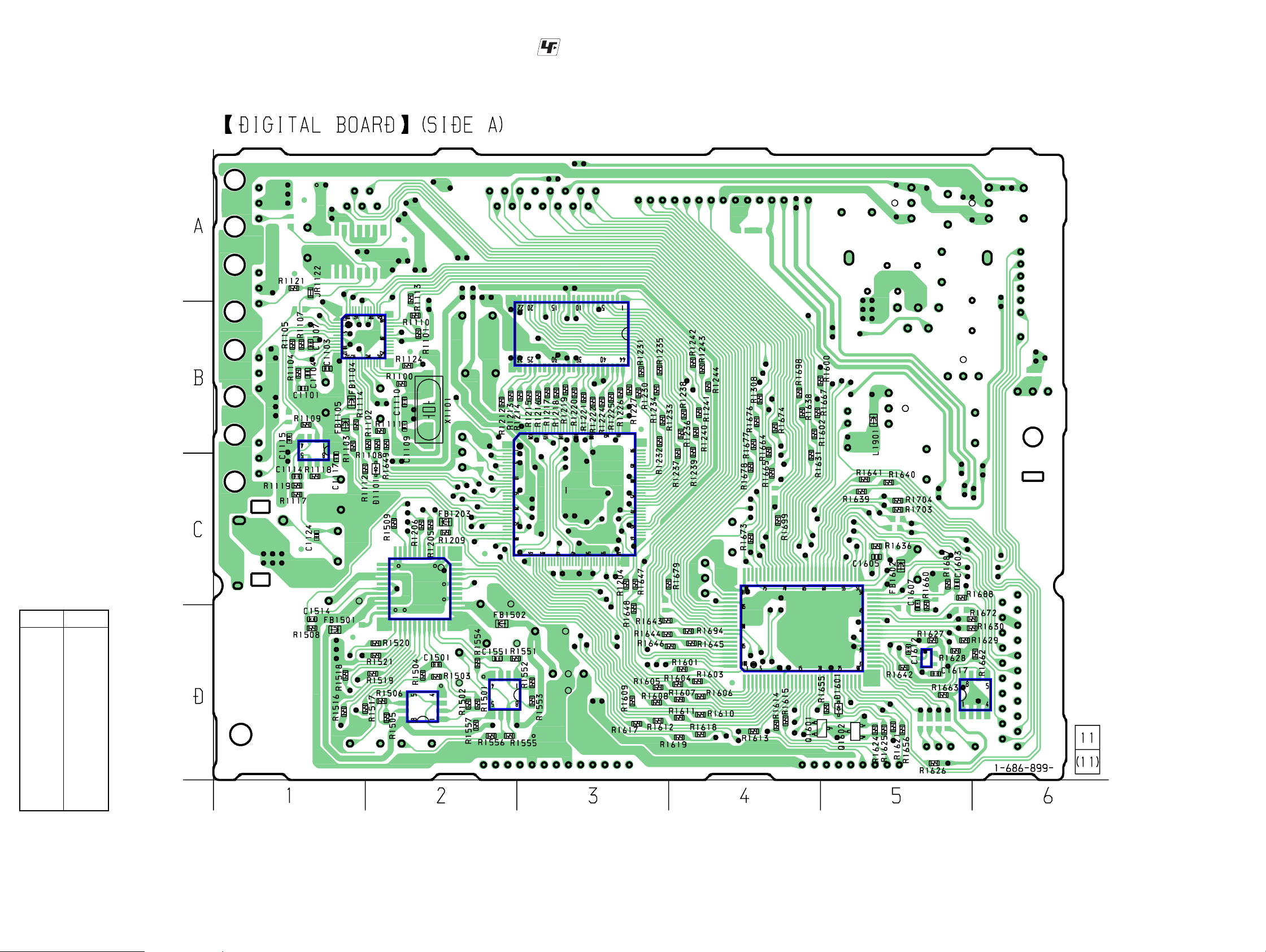
3-3. Printed Wiring Board – DIGITAL Board (SIDE A) –
• See page 7 for Circuit Boards Location.
IC1101
• : Uses unleaded solder.
IC1202
• Semiconductor
Location
Ref. No. Location
D1101 C-2
D1601 D-5
IC1101 B-2
IC1102 B-1
IC1201 C-3
IC1202 B-3
IC1501 D-2
IC1502 D-2
IC1552 D-2
IC1601 D-4
IC1602 D-5
IC1604 D-5
IC1102
11 1
12
IC1501
22
23
IC1502
IC1201
44
34
33
IC1601
5
4
IC1602
IC1552
E
E
IC1604
Q1601 D-4
Q1602 D-5
1010
STR-K650P
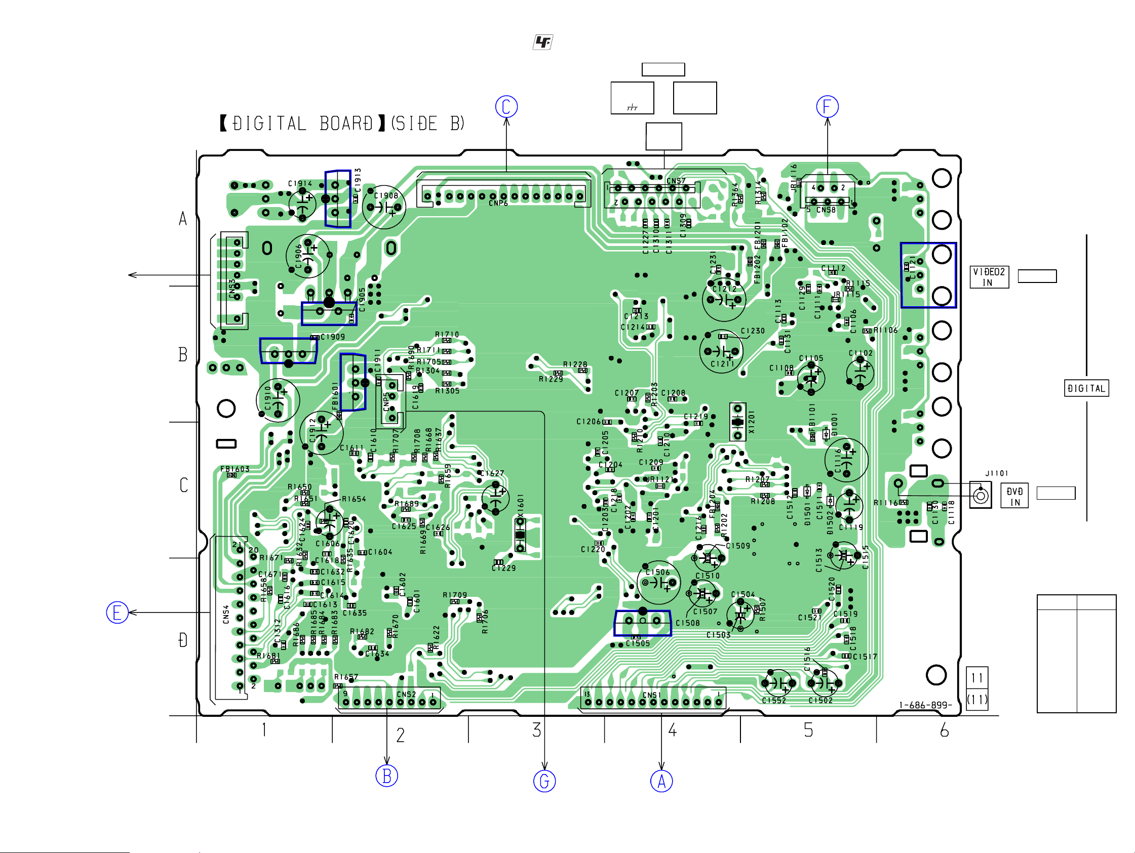
3-4. Printed Wiring Board – DIGITAL Board (SIDE B) –
7
FOR
FLASH
PROGRAMING
1
IC1901
1
54
IC1903
3
1
• See page 7 for Circuit Boards Location.
3
1
114
IC1902
3
IC1904
1
• : Uses unleaded solder.
AM
TO
MAIN
BOARD
CNP911
(Page 14)
ANTENNA
I
TUNER
PACK
FM 75Ω
COAXIAL
11
TO
VIDEO
BOARD
CNS250
(Page 21)
IC1105
3
OPTICAL
1
TO
DISPLAY
BOARD
CNS100
(Page 19)
3
3
1
COAXIAL
• Semiconductor
Location
Ref. No. Location
D1001 C-5
IC1503
13
D1501 C-5
D1502 C-5
IC1105 A-6
IC1503 D-4
IC1901 B-1
IC1902 A-1
IC1903 B-1
IC1904 B-1
TO
MAIN
BOARD
CNP502
(Page 14)
TO
STANDBY
BOARD
CNP912
(Page 18)
TO
MAIN
BOARD
CNP501
(Page 14)
1111
STR-K650P
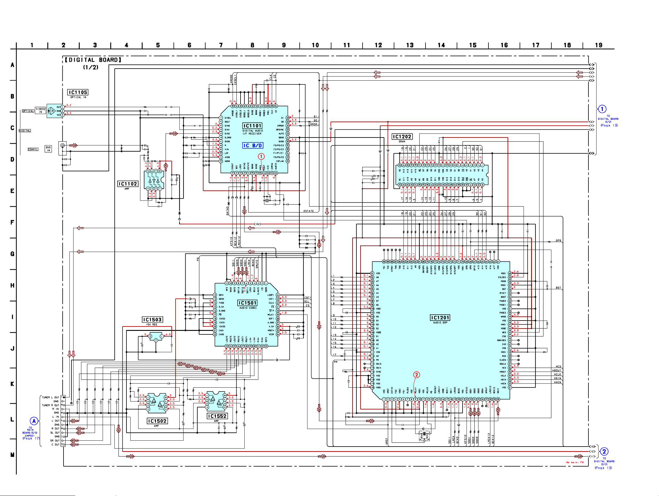
3-5. Schematic Diagram – DIGITAL Section (1/2) –
IC1105
TORX141L
J1101
JACK PIN
R1116
75
C1118
0.001
C1130
0.1
IC1102
TC7WU04F(TE12R)
220
220
R1519
0.0033
C1520
R1520
220
R1521
0.0033
C1521
13P
TP1
R1516
0.0033
C1516
0.0033
C1517
R1517
0.0033
C1518
R1518
0.0033
C1519
220
220
220
CNS1
IC1503
M5F7805L
10k
R1502
R1501
C1114
330
R1121
100
C1119
22 50V
1p
470 16V
R1503
10k
• See page 7 for Waveforms. • See page 23 for IC Block Diagrams .
C1129
0.001
C1111
0.1
R1115
C1112
0.01
10k
JR1122
0
JR1116
C1121
0
0.1
JR1115
0
0.1
C1106
5.6k
R1107
C1506
C1124
R1117
IC1502
0.1
1k
R1118R1119
560k22k
C1115
47p
C1501
NJM4565M(TE2)
R1109
100
C1505
0.1
0.0015 50V
0.1
C1117
C1107
R1106
C1101
C1104
C1116
1000
6.3V
470 10V
0.01
0.01
33k
0.1
C1513
C1515
C1514
0.1
0.1
R1104
D1001
1SS352-TPH3
FB1101
0
FB1501
R1508
100k
330
R1504
R1552
R1505
5.6k
R1506
22k
C1502
22 50V
R1105
R1551
4.7k
100
C1103
0.1
C1102
47 16V
R1102
10k
0
D1101
1SS352-TPH3
0
C1551
330
IC1552
R1553
10k
10k
C1503 C1504
0.1 10 50V
R1112
0.0015 50V
NJM4565M(TE2)
FB1104
100
R1509
1k
0
FB1105
100
R1114
4.7k
R1557
R1507
100
R1108
R1103
100
IC1501
AK4527B
4.7k
IC1101
LC89056W-E
1k
16V
R1111
330
R1554
R1555
5.6k
R1556
22k
C1552
22 50V
C1108C1105
0.147
R1100
1M
X1101
12.288MHz
C1110
18p
FB1502
C1109
18p
1SS367 -T3SONY
1SS367 -T3SONY
0
R1124
C1131
100p
100
D1502
D1501
C1510
R1101
C1512
0.022
C1508
10k
10 50V
R1113
47 16V
C1507
R1364
0
R1110
1k
1k
0.1
C1113
0.1
C1511
0.1
0.1
C1509
R1314
0
FB1102
R1212
0
C1214
0.1
FB1201
TP1220
0
220
220
R1230
R1231
TP1219
TP1218
TP1216
TP1217
C1210 C1209
R1202
100
X1201
13.59MHz
220
R1232
TP1201
0.1
220
R1233
220
R1234
FB1204
IC1202
220
R1235
IS61LV6416-10TT (ISSI)
0.1
C1213
220
220
220
R1236
R1237
R1238
IC1201
CXD9617R
0.1
0
R1205
220
R1239
TP1202
100
220
R1240
220
R1241
0
FB1203
100
R1209
0.1
C1204
100
R1206
100p
C1218
100
R1207
220
R1242
100
R1208
220
R1243
TP1203
220
R1244
TP1204
TP1215
TP1214
C1205
0.1
TP1213
TP1212
TP1211
TP1210
TP1209
TP1208
TP1207
TP1206
TP1205
C1203
0.1
R1204
1k
JR1121
0
C1220
100p
C1202
0.1
C1201
0.1
0
0.1
C1206
R1229
R1228
R1227
R1226
R1225
R1224
R1222
R1221
0.1
R1220
R1219
R1218
R1217
R1215
R1214
R1213
R1216
R1210
220
220
C1208
10k
C1207
0.1
R1203
C1219
FB1202
0.1
C1230
C1211
470 10V
C1212
470 10V
C1231
220
220
220
220
220
220
220
220
220
220
220
220
0.1
220
220
220
C1216
100p
TP1221
TP1222
10k
0.1
1212
 Loading...