

Page 1
NTE1882
Integrated Circuit
Module – AF Power Amp,
100W Min, Dual Power Supplies
Features:
D Compact packaging supports slimmer set designs
D Simpler heat sink design facilitates thermal design of slim stereo sets
D Current mirror circuit application reduces distortion to 0.08%.
D Supports addition of electronic circuits for thermal shutdown and load–short protection circuit
as well as pop noise muting which occurs when the power supply switch is turned on and off
Absolute Maximum Ratings
Maximum Supply Voltage, V
Thermal Resistance, Junction–to–Case, R
Junction Temperature, T
Operating Substrate Temperature, T
Storage Temperature Range, T
Available Time for Shorted Load (V
Recommended Operating Conditions:
Recommended Supply Voltage, V
Load Resistance, R
L
Operating Characteristics:
Parameter Symbol Test Conditions Min Typ Max Unit
Quiescent Current I
Output Power P
Total Harmonic Distortion THD PO = 1.0W, f = 1kHz – – 0.08 %
Frequency Response fL, f
Input Resistance r
Output Noise Voltage V
Midpoint Voltage V
: (TA = ±25°C unless otherwise specified)
max ±73V. . . . . . . . . . . . . . . . . . . . . . . . . . . . . . . . . . . . . . . . . . . . . . . . . .
CC
thJC
J
C
stg
= ±51V RL = 8Ω, f = 50Hz, PO = 100W), t
CC
(TA = ±25°C unless otherwise specified)
CC
(TA = ±25°C, VCC = ±51V, RL = 8Ω, VG = 40dB, Rg = 600Ω,
100k LPF ON, R
CCO
NO
VCC = ±61V 15 – 120 mA
THD = 0.08%, f = 20Hz to 20kHz 100 – – W
O
PO = 1.0W, +0dB, –3dB – 20 to 50k – Hz
H
PO = 1.0W, f = 1kHz – 55 – kΩ
i
VCC = ±61V, Rgm = 10kΩ – – 1.2 mV
VCC = ±61V –70 0 70 mV
N
(non–inductive)
L
1.1°C/W. . . . . . . . . . . . . . . . . . . . . . . . . . . . . . . . . . . . .
+150°C. . . . . . . . . . . . . . . . . . . . . . . . . . . . . . . . . . . . . . . . . . . . . . . . . . . . . . . . .
+125°C. . . . . . . . . . . . . . . . . . . . . . . . . . . . . . . . . . . . . . . . . . . . . .
–30° to +125°C. . . . . . . . . . . . . . . . . . . . . . . . . . . . . . . . . . . . . . . . . .
s
1sec. . . . . . . . .
±51V. . . . . . . . . . . . . . . . . . . . . . . . . . . . . . . . . . . . . . . . . . . . . . . . .
8Ω. . . . . . . . . . . . . . . . . . . . . . . . . . . . . . . . . . . . . . . . . . . . . . . . . . . . . . . . . . . . . . . . .
rms
Note 1 Output noise voltage represents the peak value on the rms scale (VTVM). The noise voltage wave-
form does not include the pulse noise.
Page 2
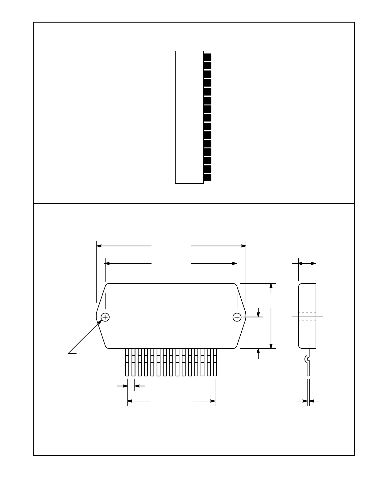
Pin Connection Diagram
(Front View)
15
Bootstrap
V (+)
14
13
Output
V (–)
12
11 Compensation
I
10
Adjust
Emitter Bypass
9
Compensation
8
I
7
Adjust
Test Point
6
Bypass
5
Bias
4
Substrate
3
NFB
2
Input
1
.141 (3.6)
Dia (2 Holes)
2.520 (64.0)
2.190 (55.6)
.334 (8.5)
1.440
(36.4)
.737
(18.7)
115
.100 (2.54)
.020(.508)1.400 (35.56)
 Loading...