

Sony STK433 Service Manual
Ordering number : EN*A1487
Thick-Film Hybrid IC
STK433-060-E
Overview
The STK433-060-E is a hybrid IC designed to be used in 50W × 2ch class AB audio power amplifiers.
Applications
• Audio power amplifiers.
Features
• Pin-to-pin compatible outputs ranging from 30W to 60W.
• Can be used to replace the STK433-100 series (80W to 150W/2ch)and STK433-200/-300 series (3-channel)
due to its pin compatibility
• Miniature package (47.0mm × 25.6mm × 9.0mm)
• Output load impedance: RL = 6Ω to 4Ω supported
• Allowable load shorted time: 0.3 second
• Allows the use of predesigned applications for standby and mute circuits.
Series Models
STK433-030-E STK433-040-E STK433-060-E STK433-070-E
Output 1 (10%/1kHz) 30W×2 channels 40W×2 channels 50W×2 channels 60W×2 channels
Output 2 (0.4%/20Hz to 20kHz) 20W×2 channels 25W×2 channels 35W×2 channels 40W×2 channels
Max. rated VCC (quiescent) ±34V ±38V ±46V ±50V
Max. rated VCC (6Ω) ±32V ±36V ±40V ±44V
Max. rated VCC (4Ω) ±26V ±30V ±33V ±37V
Recommended operating VCC (6Ω) ±21V ±24V ±27V ±29V
Dimensions (excluding pin height) 47.0mm×25.6mm×9.0mm
2-channel class AB audio power IC
50W+50W
,
Any and all SANYO Semiconductor Co.,Ltd. products described or contained herein are, with regard to
"standard application", intended for the use as general electronics equipment (home appliances, AV equipment,
communication device, office equipment, industrial equipment etc.). The products mentioned herein shall not be
intended for use for any "special application" (medical equipment whose purpose is to sustain life, aerospace
instrument, nuclear control device, burning appliances, transportation machine, traffic signal system, safety
equipment etc.) that shall require extremely high level of reliability and can directly threaten human lives in case
of failure or malfunction of the product or may cause harm to human bodies, nor shall they grant any guarantee
thereof. If you should intend to use our products for applications outside the standard applications of our
customer who is considering such use and/or outside the scope of our intended standard applications, please
consult with us prior to the intended use. If there is no consultation or inquiry before the intended use, our
customer shall be solely responsible for the use.
Specifications of any and all SANYO Semiconductor Co.,Ltd. products described or contained herein stipulate
the performance, characteristics, and functions of the described products in the independent state, and are not
guarantees of the performance, characteristics, and functions of the described products as mounted in the
'
customer
device, the customer should always evaluate and test devices mounted in the customer
equipment.
s products or equipment. To verify symptoms and states that cannot be evaluated in an independent
'
sproductsor
O2109HKIM No. A1487-1/11
STK433-060-E
Specifications
Absolute Maximum Ratings at Ta = 25°C (excluding rated temperature items), Tc=25°C unless otherwise specified
Parameter Symbol Conditions Ratings Unit
Maximum quiescent supply voltage 0 VCC max (0) When no signal
Maximum supply voltage 1 VCC max (1) RL≥6Ω
Maximum supply voltage 2 VCC max (2) RL=4Ω
Minimum operating supply voltage VCC min
Pin 13 input voltage VST max
Thermal resistance θj-c Per power transistor
Junction temperature Tj max Both the Tj max and Tc max conditions must be met.
IC substrate operating temperature Tc max
Storage temperature Tstg
Allowable load shorted time *4 ts VCC=±27V, RL=6Ω, f=50Hz, PO=35W,
1-channel active
Operating Characteristics at Tc=25°C, R
=6Ω, Rg=600Ω, VG=30dB, non-inductive load RL, unless otherwise
L
specified
Conditions *2 Ratings
Parameter Symbol
Output power *1
Total harmonic distortion *1
Frequency characteristics *1 fL, fH
Input impedance ri
Output noise voltage *3 VNO
Quiescent current I
Standby current I
Output neutral voltage VN
Pin 13 voltage when standby
ON
Pin 13 voltage when standby
OFF
PO (1)
PO (2)
PO (3)
THD (1)
THD (2)
CCO
CST
VST ON
VST OFF
VCC
(V)
±27 20 to 20k 0.4 33 35
±27 1k 10 50
±22 1k 1 RL=4Ω 35
±27 20 to 20k 0.4
±27 1k
±27 1.0 +0 -3dB 20 to 50k Hz
±27 1k 1.0 55 kΩ
±33 Rg=2.2kΩ 1.0 mVrms
±33 No loading 20 45 70 mA
±33 1 mA
±33 -70 0 +70 mV
±27 Standby 0.6 V
±27 Operating 2.5 V
f
(Hz)
PO
(W)
5.0
THD
(%)
min typ max
0.02
[Remarks]
*1: For 1-channel operation
*2: Unless otherwise specified, use a constant-voltage power supply to supply power when inspections are carried out.
*3: The output noise voltage values shown are peak values read with a VTVM. However, an AC stabilized (50Hz)
power supply should be used to minimize the influence of AC primary side flicker noise on the reading.
*4: Use the transformer power supply circuit shown in the figure below for allowable load shorted time measurement.
*5: Please connect -preVCC Pin (#1 pin) with the stable minimum voltage and connect so that current does not flow in
by reverse bias.
* Thermal design must be implemented based on the conditions under which the customer’s end products are expected
to operate on the market.
* A thermoplastic adhesive is used to adhere the case.
±46 V
±40 V
±33 V
±10 V
-0.3 to +5.5 V
3.5 °C/W
150 °C
125 °C
-30 to +125 °C
0.3 s
unit
W
%
Designated transformer power supply
(MG-200 equivalent)
DBA40C
10000μF
+
+
10000μF
500Ω
500Ω
+V
-V
CC
CC
No. A1487-2/11
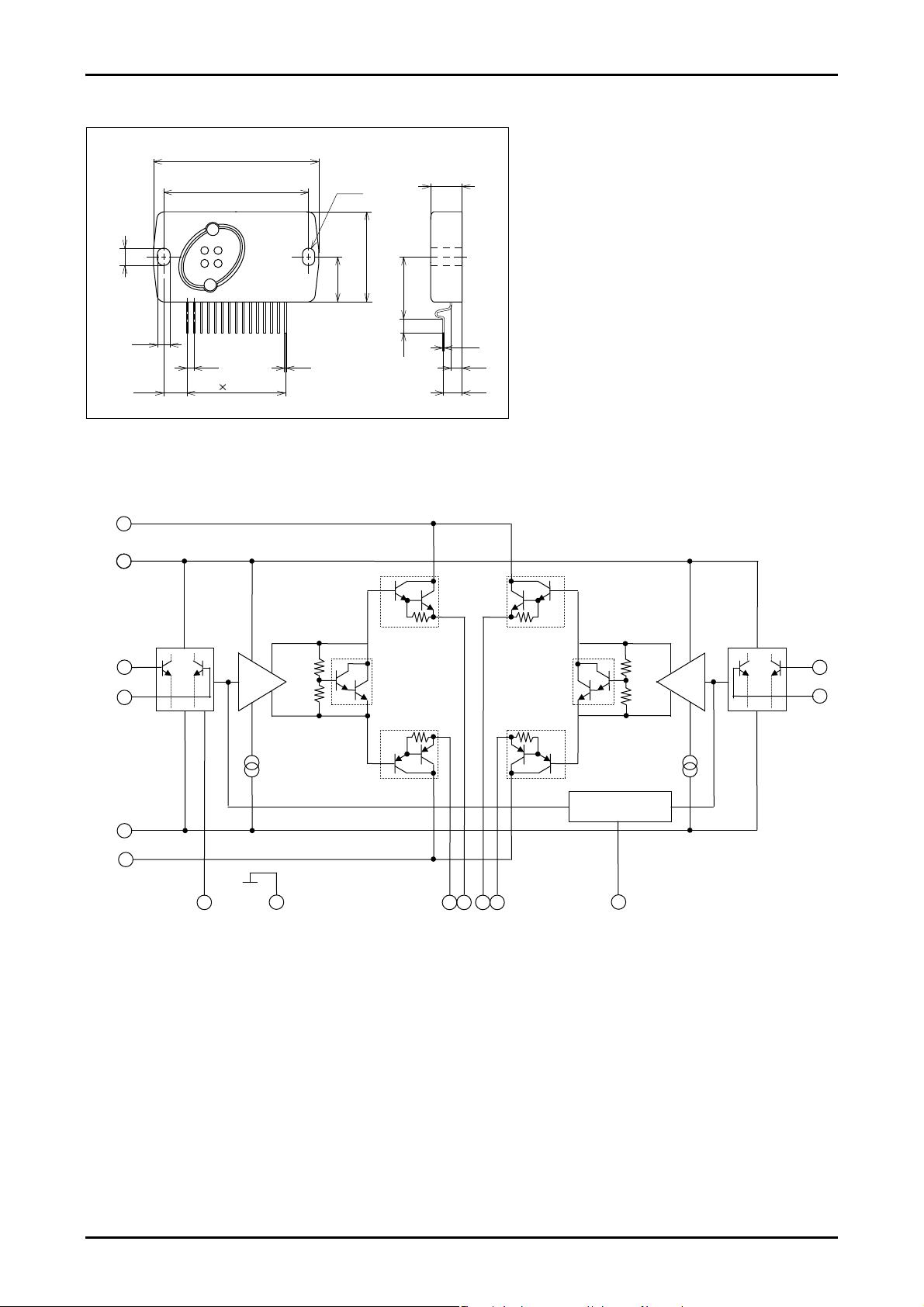
Package Dimensions
unit:mm (typ)
47.0
41.2
5.0
115
3.6
(6.6)
2.0
14 2.0=28.0
0.5
Internal Equivalent Circuit
3
8
(R1.8)
12.8
STK433-060-E
9.0
25.6
17.6
4.0
0.4
2.9
5.5
11
12
Pre Driver
CH1
+
-
Bias Circuit
1
2
SUB
10
9
5
7
6
4
13
Pre Driver
CH2
15
+
14
-
No. A1487-3/11
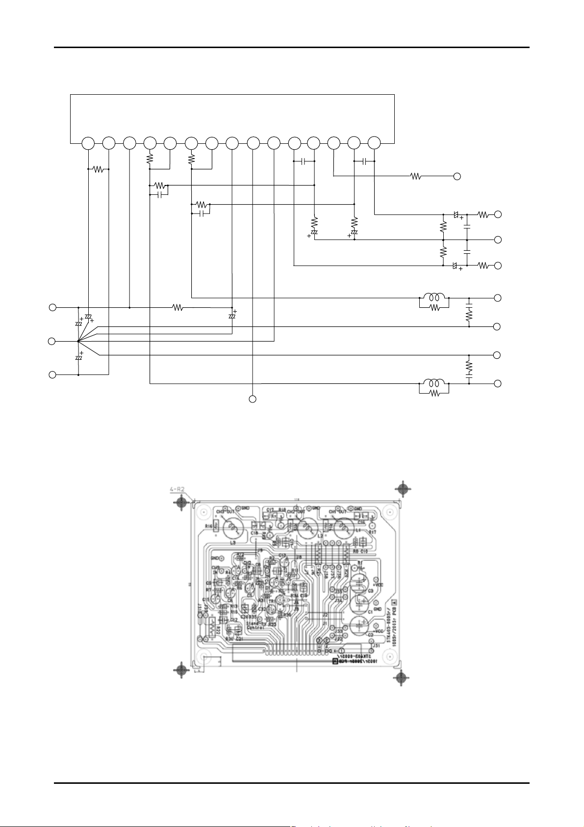
Application Circuit Example
Ch1
-VCC
-PRE
2 3 4
+VCC
100Ω
OUT
0.22Ω
56kΩ
Ch1
OUT
5
3pF
+VCC
100μF
GND
100μF
/50V
/50V
100μF
/50V
100Ω/1W
-VCC
Sample PCB Trace Pattern
STK433-060-E
STK433-060-E
Ch1
Ch2
OUT
Ch2
OUT
SUB GND+PRE
Ch1
IN
NF
6 7 8 9 10 11 12 13 141 15
0.22Ω
100pF
56kΩ
3pF
100μF
/50V
10μF
/10V
SUB.GND
ST-BY
1.8kΩ
Ch2
NF
100pF
1.8kΩ
10μF
/10V
Ch2
IN
Stand-by Control
2.2μF
/50V
56kΩ 56kΩ
3μH
4.7Ω
3μH
4.7Ω
2.2μF
/50V
470pF
470pF
1kΩ
0.1μF
4.7Ω/1W
4.7Ω/1W
0.1μF
1kΩ
Ch2 IN
GND
Ch1 IN
Ch2 OUT
GND
GND
Ch1 OUT
No. A1487-4/11
 Loading...