

Sony SSS-55-HDE, NASS-55-HDE Service manual
NAS-S55HDE/SS-S55HDE
SERVICE MANUAL
Ver. 1.0 2008.03
• SS-S55HDE is the speaker system of
NAS-S55HDE.
• AEP model is the HDD network audio
system of NAS-SC55PKE.
• UK model is the HDD network audio
system of NAS-SC55PKE and single
sales model.
Trademarks, etc.
•
Independent JPEG Group.
•
ATR AC an d
Corporation.
•
“WALKMAN”,
registered trademarks of Sony Corporation.
•
“GIGA JUKE” and its logo are trademarks of Sony
Corporation.
•
US and foreign patents licensed from Dolby Laboratories.
•
MPEG Layer-3 audio coding technology and patents
•
Corporation in the United States and/or other countries.
•
technology outside of this product is prohibited without
subsidiary.
•
•
by MORISAWA & COMPANY LTD.
COMPANY LTD., and the copyright of the font also
belongs to MORISAWA & COMPANY LTD.
•
BuiltwithLinterDatabase.
Copyright © 2006-2007, Brycen Corp., Ltd.
Copyright © 1990-2003, Relex, Inc., All rights reserved.
•
Music recognition technology and related data are provided
by Gracenote®. Gracenote is the industry standard in music
recognition technology and related content delivery. For
more information, please visit www.gracenote.com.
CD and music-related data from Gracenote, Inc., copyright
practice one or more of the following U.S. Patents:
#5,987,525; #6,061,680; #6,154,773, #6,161,132, #6,230,192,
#6,230,207, #6,240,459, #6,330,593, and other patents issued
or pending. Some services supplied under license from
Open Globe, Inc. for U.S. Patent: #6,304,523.
Gracenote and CDDB are registered trademarks of
“Powered by Gracenote” logo are trademarks of Gracenote.
are trademarks of Sony
and are
CD
Section
HD
Section
DIN power output (rated):
40 + 40 W (6
Continuous RMS power output (reference):
50 + 50 W (6
Music Power output (reference):
50 + 50 W (6
CD player section
System:
Compact disc and digital audio system
Laser Diode Properties:
Emission duration: continuous
Laser Output*
1
*
distance of 200 mm from the objective lens
surface on the Optical Pick-up Block with
7 mm aperture.
Frequency response:
20 Hz - 20 kHz (±0.5 dB)
Model Name Using Similar Drive
CD-ROM Drive Name
Model Name Using Similar Drive
Hard Disk Drive Name
Ω at 1 kHz, DIN)
Ω at 1 kHz, 10 % THD)
Ω at 1 kHz, 10 % THD)
1
: Less than 44.6 μw
AEP Model
UK Model
NAS-50HDE
CD-5010A-020
NEW
HDD/SG-NIGHTHAWK-S (80GB)
SPECIFICATIONS
Total harmonic distortion:
Less than 0.1 %
HDD Jukebox section
Capacity:
1
80 GB*
*1A portion of the memory is used for system
management functions. Actual available
memory is approx. 68 GB (73,014,444,032 bytes).
Recording format:
MP3
Linear PCM
Importing format*1:
MP3 (“.mp3”, “.oma”)
Linear PCM (“.wav”, “.oma”)
WMA (“.wma”, “.oma”)
at a
ATRAC (“.oma”)
1
*
WMA Professional, WMA Lossless, WMA
Voice, and
WMA formats:
Management).
– Continued on next page –
NAS-S55HDE
HDD NETWORK AUDIO SYSTEM
SS-S55HDE
9-889-036-01
2008C05-1
2008.03
©
SPEAKER SYSTEM
Sony Corporation
Audio Business Group
Published by Sony Techno Create Corporation
NAS-S55HDE/SS-S55HDE
Maximum recording time (measured
with ATRAC 48 kbps):
About 3,400 h
Maximum number of tracks:
40,000
FM tuner section
Tuner:
FM stereo tuner
Frequency range:
87.5 - 108.0 MHz (50 kHz step)
Antenna:
FM wire antenna
Antenna terminals:
Ω unbalanced
75
Intermediate frequency:
10.7 MHz
AM tuner section
Tuner:
AM tuner
Frequency range:
531 - 1,602 kHz (with the interval
set at 9 kHz)
Antenna:
AM loop antenna
Antenna terminals:
External antenna terminal
Intermediate frequency:
450 kHz
DAB tuner section (UK
model only)
Tuner:
DAB stereo tuner
Antenna:
DAB wire antenna
Antenna terminals:
Ω unbalanced
75
Frequency range:
Band-III: 174.928 (5A) – 239.200
(13F) MHz
DAB frequency table (Band-III):
Frequency Label
174.928 MHz 5A
176.640 MHz 5B
178.352 MHz 5C
180.064 MHz 5D
181.936 MHz 6A
183.648 MHz 6B
185.360 MHz 6C
187.072 MHz 6D
188.928 MHz 7A
190.640 MHz 7B
192.352 MHz 7C
194.064 MHz 7D
195.936 MHz 8A
197.648 MHz 8B
199.360 MHz 8C
201.072 MHz 8D
202.928 MHz 9A
204.640 MHz 9B
Frequency Label
206.352 MHz 9C
208.064 MHz 9D
209.936 MHz 10A
211.648 MHz 10B
213.360 MHz 10C
215.072 MHz 10D
216.928 MHz 11A
218.640 MHz 11B
220.352 MHz 11C
222.064 MHz 11D
223.936 MHz 12A
225.648 MHz 12B
227.360 MHz 12C
229.072 MHz 12D
230.784 MHz 13A
232.496 MHz 13B
234.208 MHz 13C
235.776 MHz 13D
237.488 MHz 13E
239.200 MHz 13F
Inputs/Outputs
MONITOR OUT (phono jack):
1 Vp-p, 75
AUDIO IN (top: stereo mini jack) / AUDIO
IN (rear: phono jacks):
Voltage 0.8 V (standard),
impedance 10 k
(low sensitivity), impedance 10 k
(rear)
NETWORK port:
10BASE-T/100BASE-TX
USB port:
USB type A, Hi-Speed USB for
connecting USB devices such as
“WALKMAN”
DMPORT
Output voltage: DC 5 V
mA
PHONES jack (stereo mini jack):
Accepts headphones of 8
more
Ω unbalanced (NTSC)
Ω (top) / 1.5 V
Ω or
Speaker
Speaker system:
Speaker units:
Woofer: 120 mm, cone type
Nominal impedance:
Ω
6
Dimensions (w/h/d)
Approx. 140 × 283 × 245 mm
(including a grille)
Mass
Approx. 2.8 kg net per speaker
Wireless adaptor
Interface:
IEEE802.11 b/g-compliant
2.4 GHz radio frequency band
General
Power requirements:
230 V AC, 50/60 Hz
Power consumption:
65 W (0.5 W or lower at the
standard (power save) mode)
Dimensions (w/h/d) (including
projecting parts and controls):
UK model:
With the display window lowered:
approx. 285 × 143 × 317.4 mm
With the display window raised:
approx. 285 × 193 × 317.4 mm
Models except the UK model
With the display window lowered:
approx. 285 × 143 × 311 mm
With the display window raised:
approx. 285 × 193 × 311 mm
Mass (Approx.):
5.0 kg
Operating temperature:
o
+5
C (+41 oF) to +35 oC (+95 oF)
Operating humidity:
25 % to 80 %
Supplied accessories:
Wireless adaptor (1)
USB extension cable (1)
Speaker codes (2)
Speaker pads (8)
AM loop antenna (1)
FM wire antenna (1)
DAB wire antenna (1) (for the
UK model only)
Remote control (1)
R6 (size AA) batteries (2)
Operating Instructions (this manual)
GNU General Public License/GNU
Lesser General Public License (1)
License agreement for SONY
soware (1)
subjecttochangewithoutnotice.
About the self-diagnosis function
A service number consisting of
E 00 11) appears in the display
Ω
service number appears, consult the local
authorized service facility and report this service
number to the service personnel.
Notes on chip component replacement
• Never reuse a disconnected chip component.
• Notice that the minus side of a tantalum capacitor may be damaged by heat.
Flexible Circuit Board Repairing
• Keep the temperature of soldering iron around 270 °C during
repairing.
• Do not touch the soldering iron on the same conductor of the
circuit board (within 3 times).
• Be careful not to apply force on the conductor when soldering
or unsoldering.
CAUTION
Use of controls or adjustments or performance of procedures other than
those specifi ed herein may result in hazardous radiation exposure.
SAFETY-RELATED COMPONET WARNING!
COMPONENTS IDENTIFIED BY MARK 0 OR DOTTED LINE
WITH MARK 0 ON THE SCHEMATIC DIAGRAMS AND IN
THE PARTS LIST ARE CRITICAL TO SAFE OPERATION.
REPLACE THESE COMPONENTS WITH SONY PARTS
WHOSE PART NUMBERS APPEAR AS SHOWN IN THIS
MANUAL OR IN SUPPLEMENTS PUBLISHED BY SONY.
when the self-diagnosis
function activates to prevent
abnormal operation. When this
This appliance is
classified as a CLASS 1
LASER product. This
marking is located on the
rear exterior.
2

TABLE OF CONTENTS
NAS-S55HDE/SS-S55HDE
1. SERVICING NOTES ............................................. 4
2. GENERAL .................................................................. 9
3. DISASSEMBLY
3-1. Disassembly Flow ........................................................... 12
3-2. Panel (Side L/R) Assy ..................................................... 13
3-3. Cover (Base) Assy, Panel (Top) Block ........................... 13
3-4. PANEL (TOP) Board, LCD Block .................................. 14
3-5. Module (LCD) ................................................................ 14
3-6. Panel (Front) Block ......................................................... 15
3-7. Knob (VOL), PANEL (TOP) Board ............................... 15
3-8. Chassis (Top) .................................................................. 16
3-9. MOTHER Board ............................................................. 16
3-10. SP/DM Board .................................................................. 17
3-11. MAIN Board ................................................................... 17
3-12. Hard Disc Drive .............................................................. 18
3-13. Fan. DC (M101), Chassis (MID) .................................... 18
3-14. CD Block ........................................................................ 19
3-15. Note the CD-ROM Drive and
Insulating (CD) Replacing .............................................. 19
3-16. CD-ROM Drive (CD-5010A-020) .................................. 20
3-17. Position of Frrite Core for Speaker Cord ........................ 20
4. TEST MODE ............................................................ 21
5. DIAGRAMS
5-1. Block Diagram - MAIN Section - ................................... 23
5-2. Block Diagram - PANEL, DSP Section -........................ 24
5-3. Block Diagram - AUDIO Section - ................................. 25
5-4. Block Diagram - POWER SUPPLEY Section - ............. 26
5-5. Printed Wiring Board
- MOTHER Board (Component Side) - .......................... 28
5-6. Printed Wiring Board
- MOTHER Board (Conductor Side) - ........................... 29
5-7. Schematic Diagram - MOTHER Board (1/10) - ............. 30
5-8. Schematic Diagram - MOTHER Board (2/10) - ............. 31
5-9. Schematic Diagram - MOTHER Board (3/10) - ............. 32
5-10. Schematic Diagram - MOTHER Board (4/10) - ............. 33
5-11. Schematic Diagram - MOTHER Board (5/10) - ............. 34
5-12. Schematic Diagram - MOTHER Board (6/10) - ............. 35
5-13. Schematic Diagram - MOTHER Board (7/10) - ............. 36
5-14. Schematic Diagram - MOTHER Board (8/10) - ............. 37
5-15. Schematic Diagram - MOTHER Board (9/10) - ............. 38
5-16. Schematic Diagram - MOTHER Board (10/10) - ........... 39
5-17. Printed Wiring Board
- MAIN Board (Component Side) - ................................ 40
5-18. Printed Wiring Board
- MAIN Board (Conductor Side) - .................................. 41
5-19. Schematic Diagram - MAIN Board (1/4) - ..................... 42
5-20. Schematic Diagram - MAIN Board (2/4) - ..................... 43
5-21. Schematic Diagram - MAIN Board (3/4) - ..................... 44
5-22. Schematic Diagram - MAIN Board (4/4) - ..................... 45
5-23. Printed Wiring Board - DAB PS Board (UK Model) - ... 46
5-24. Schematic Diagram - DAB PS Board (UK Model) - ...... 46
5-25. Printed Wiring Board - SP/DM Board - .......................... 47
5-26. Schematic Diagram - SP/DM Board - ............................ 47
5-27. Printed Wiring Board - PANEL (FRONT) Board - ........ 48
5-28. Schematic Diagram - PANEL (FRONT) Board - ........... 48
5-29. Printed Wiring Board - PANEL (TOP) Board - .............. 49
5-30. Schematic Diagram - PANEL (TOP) Board - ................. 49
5-31. Printed Wiring Board - LCD Board - .............................. 50
5-32. Schematic Diagram - LCD Board - ................................ 51
5-33. Printed Wiring Boards
- AUDIO INPUT/OUTPUT Section -............................. 52
5-34. Schematic Diagram
- AUDIO INPUT/OUTPUT Section -............................. 52
6. EXPLODED VIEWS
6-1. Front Panel Section ......................................................... 82
6-2. Panel (Top) Section ......................................................... 83
6-3. LCD Section ................................................................... 84
6-4. MAIN Board, MOTHER Board Section ........................ 85
6-5. HDD Section ................................................................... 86
6-6. CD-ROM Drive, Chassis Section ................................... 87
6-7. Speaker Section (SS-S55HDE) ....................................... 88
7. ELECTRICAL PARTS LIST .............................. 89
3
NAS-S55HDE/SS-S55HDE
SECTION 1
SERVICING NOTES
NOTES ON HANDLING THE OPTICAL PICK-UP
BLOCK OR BASE UNIT
The laser diode in the optical pick-up block may suffer electrostatic break-down because of the potential difference generated by the
charged electrostatic load, etc. on clothing and the human body.
During repair, pay attention to electrostatic break-down and also
use the procedure in the printed matter which is included in the
repair parts.
The fl exible board is easily damaged and should be handled with
care.
NOTES ON LASER DIODE EMISSION CHECK
The laser beam on this model is concentrated so as to be focused
on the disc refl ective surface by the objective lens in the optical
pickup block. Therefore, when checking the laser diode emission,
observe from more than 30 cm away from the objective lens.
UNLEADED SOLDER
Boards requiring use of unleaded solder are printed with the leadfree mark (LF) indicating the solder contains no lead.
(Caution: Some printed circuit boards may not come printed with
the lead free mark due to their particular size)
: LEAD FREE MARK
Unleaded solder has the following characteristics.
• Unleaded solder melts at a temperature about 40 °C higher
than ordinary solder.
Ordinary soldering irons can be used but the iron tip has to be
applied to the solder joint for a slightly longer time.
Soldering irons using a temperature regulator should be set to
about 350 °C.
Caution: The printed pattern (copper foil) may peel away if the
heated tip is applied for too long, so be careful!
• Strong viscosity
Unleaded solder is more viscou-s (sticky, less prone to fl ow)
than ordinary solder so use caution not to let solder bridges
occur such as on IC pins, etc.
• Usable with ordinary solder
It is best to use only unleaded solder but unleaded solder may
also be added to ordinary solder.
NOTE THE CN400 ON THE DAB PS BOARD REPLACING
CN400 on the DAB PS board cannot exchange with single. When
CN400 on the DAB PS board is damaged, exchange the entire
mounted board.
About the Hard Disk Drive
Because of its high storage density, the hard disk can read and
write data a very high speeds.
It is, however, easily damaged by mechanical vibration, shock, or
dust. Although the hard disk is equipped with safety mechanisms
to prevent the lost of data due to these factors, the following
precautionsshouldbetakenduringthehandlingofthe unit.
• Donotsubjectthe unittostrongshocksorvibrations.
• Do not place the unit in a location subject to mechanical
vibration or at an unstable location.
• Do not move the unit while the power cord is connected to a
wall outlet.
• Do not disconnect the power cord while the unit is recording or
playing a track.
• Do not use the unit in a place subject to extreme changes in
temperature (a temperature gradient greater than 18°F (10°C)/
hour).
• Do not attempt to replace or upgrade the hard disk drive by
yourself, as this may cause the unit to malfunction.
Sony cannot provide compensation for any loss of data caused by a
damaged hard disk drive.
On data back up
Audio data and system settings stored on the unit’s hard disk may
be lost during repairs done to the unit. Before taking the unit in for
repairs, it is recommended that you record the settings on a piece
of paper and that you use the Back Up function to back up the data
to a shared folder on your computer or a USB hard disk drive (see
“Backing up and restoring audio data” on page 104).
Data on the unit’s HDD is subject to damage during normal
operations. To prevent the loss of data, you should back up the data
on a regular basis. Please note that we cannot take responsibility
for any data that may be lost or
repairs.
Cleaning the cabinet
slightly moistened with a mild
detergent solution. Do not use any type of abrasive pad, scouring
powder, or solvent, such as thinner, benzine, or alcohol.
Note on the power cord
Before you unplug the power cord from the wall outlet, make sure
that the unit is in standby mode (the On/Standby indicator is lit up
red or orange). If you unplug the power cord while the unit is
operating (the On/Standby indicator lit up green), data that was
recorded may be lost or the unit may malfunction.
NOTE THE CN5002, IC501, IC1001, IC1002, IC2001,
IC2101, IC5001, IC9101, IC9201, IC9301 AND IC9401
ON THE MOTHER BOARD REPLACING
CN5002, IC501, IC1001, IC1002, IC2001, IC2101, IC5001,
IC9101, IC9201, IC9301 and IC9401 on the MOTHER board cannot exchange with single. When CN5002, IC501, IC1001, IC1002,
IC2001, IC2101, IC5001, IC9101, IC9201, IC9301 and IC9401 on
the MOTHER board are damaged, exchange the entire mounted
board.
4
NAS-S55HDE/SS-S55HDE
Notes on CDs
v Do not scratch or attach stickers to the surface of the disc.
v CDs with non-standard shapes (e.g., a star, heart, or square)
cannot be played on this unit. Attempting to do so may damage
the unit.
v When cleaning the disc, use a cleaning cloth and wipe the disc
from the center out to the edge. If the disc is extremely dirty,
wipe the disc with a slightly moistened cloth, followed by a dry
cloth. Do not clean a disc with a benzine thinner, commercial
cleaners or anti-static sprays intended for vinyl LPs.
v Do not place discs in hot places, including places exposed to
direct sunlight, near heat sources such as hot air ducts, or inside
parked cars.
v Do not use a rental or second-hand disc on which glue that
spread from under the label attached to it. If you do, there is a
chance that the disc may become stuck to parts within the unit,
causingittomalfunction.
v Do not use a commercial cleaning disc as it may cause the unit
to malfunction.
Music discs encoded with copyright protection technologies
playback discs that conform to
playback discs that conform to the Compact Disc (CD) standard.
Recently, various music discs encoded with copyright protection
technologies are marketed by some record companies. Please be
aware that among those discs, there are some that do not conform
tothe CD standardandmaynotbeplayablebythisproduct.
Note on DualDiscs
A DualDisc is a two sided disc product which mates DVD
recorded material on one side with digital audio material on the
other side. However, since the audio material side does not conform
to the Compact Disc (CD) standard, playback on this product is
not guaranteed.
About CDs
The unit CAN play the following discs
v CDs:
Music CDs, CD-Rs, CD-RWs and CD TEXT
v
CD-ROMs, CD-Rs and CD-RWs (recorded in a format
conforming to the ISO 9660 Level 1 or 2, or Joliet standards).
Multisession CDs are supported.
Notes
v If the disc begins with a CD-DA (or “ATRAC”/MP3) session, it
is recognized as a CD-DA (or “ATRAC”/MP3) disc, and other
sessions are not played back.
v A disc with a mixed CD format is recognized as a CD-DA
(audio) disc.
v Some CD-Rs or CD-RWs may not be played on this unit,
depending on its characteristics and the recording conditions.
v CD-RWs may require some time
is because they have a lower
of discs.
v In the case of discs containing more than 500 tracks of audio
data, the unit will not recognize track 501 or above.
v Discs with many directories or a complicated structure may
require some time before they start playing. When recording
albums to a disc, it is recommended that recording will be done
no deeper than the sub-directory 2 level.
Tip
For details on writing data to a disc, refer to the operating manual
supplied with the CD-R/RW drive
Notes on playing MP3 discs
v
or 48 kHz and a bit rate of 32 to 320 kbps. If you play a
playback may stop, loud noises or sound skipping may occur, or
the speakers may be damaged.
v
v
v Under the following conditions, the actual elapsed time or the
remaining time of an MP3
displayed.
— When playing a VBR
— When performing a fast forward or fast rewind operation
format, a sampling rate of 32, 44.1,
sampling rate or bit rate on this unit,
malfunction may occur.
recorded in the MP3 Pro format.
5
NAS-S55HDE/SS-S55HDE
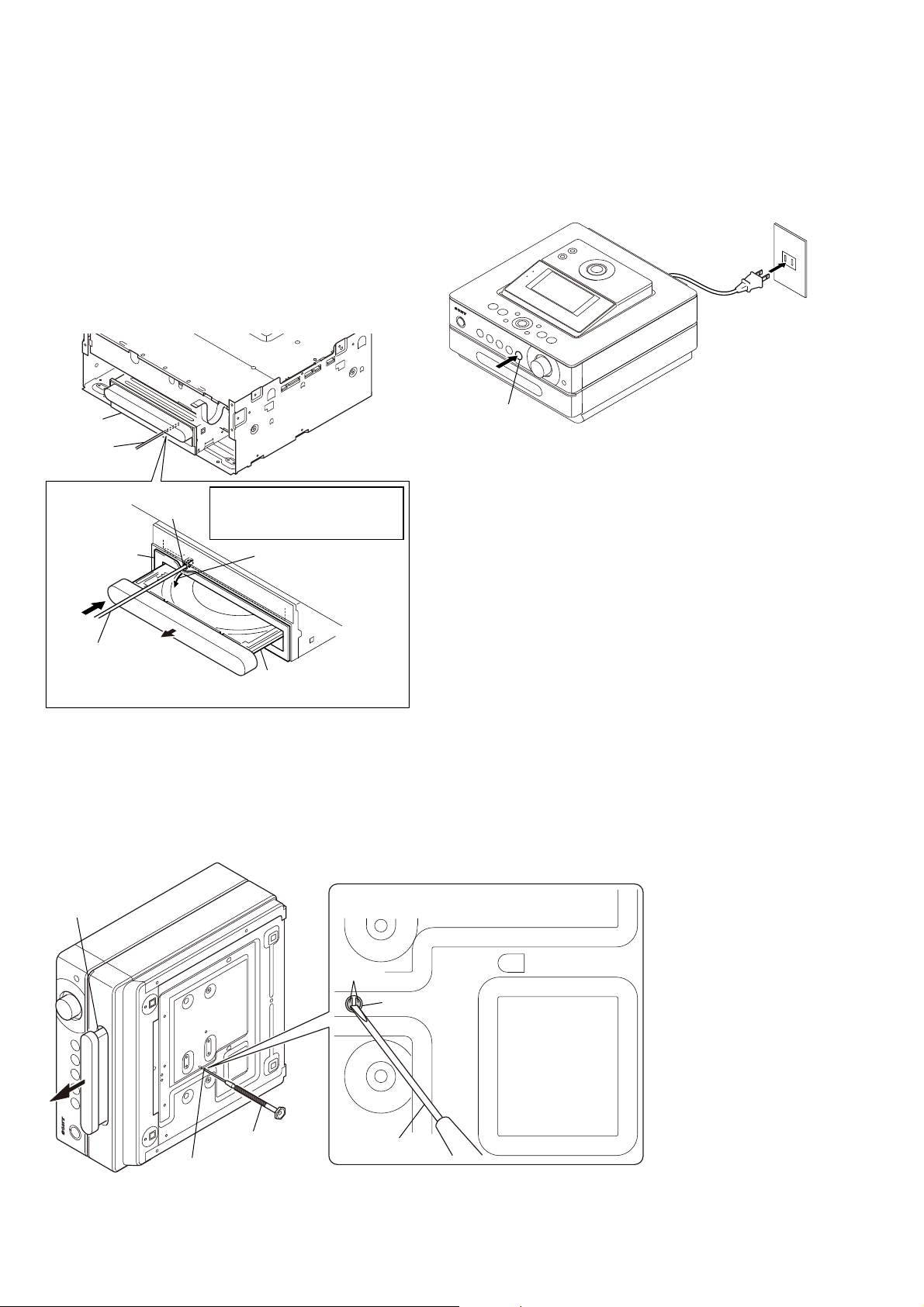
HOW TO DRAW OUT FORCIBLY THE DISC TRAY
In the event that the disc tray does not come out due to any failure, three methods are available to draw it out forcibly. Use either
method described below according to the symptom.
METHOD 1
If the power did not turn on or if the power is OFF:
1. With the power cord unplugged, remove the panel (side L) /
(side R) assembly, panel (top), and panel (front). (See “How to
Remove 2-2, 2-3 (page 8), 2-6 (page 10)”)
2. As shown in the fi gure, insert a thin rod into the hole at the
lower part of CD block, and push it in the arrow A direction.
CD cection
thin rod
hole
cushion (CD)
Note: This illustration shows the
disc tray as viewed from
the bottom.
Peel the cushion (CD) a
little when it hides the hole.
METHOD 3
If the mother board starts but the system software is abnormal:
Plug in the power cord while pressing the [Z] button.
Note: This method is same as “CD Start Mode” of test modes. Load the
start disc and close the disc tray, and if the start disc is not recognized, start the CD as usual.
power cord
botton
;
"
Insert a thin rod into the
hole and push it in the
arrow" direction.
(Disc tray will come out)
disc tray
METHOD 2
If the CD-ROM drive is turned on but the mother board does not
start:
1. Insert a thin fl at-tip screwdriver into a round hole at the bottom
of the set.
2. Through a hole at the bottom of CD-ROM drive, short the
points (patterns) on the board of CD-ROM drive.
disc tray
Short across patterns with a flap-tip screwdriver.
pattern
round hole
flat-tip screwdriver
round hole
flat-tip screwdriver
6
NAS-S55HDE/SS-S55HDE
DISCHARGE PROCESSING
1. Switching power block on primary side of main board
Though high voltage of 280V is applied to the electrolytic capacitor (C205), in about 3 seconds after the AC cord was unplugged, the
voltage will lower to 3 to 4V.
However, in the case of standalone main board, the discharge time will be long because of small load.
The voltage at this time is about 290V.
The voltage becomes half in about 20 seconds after the AC cord was unplugged. After that, in about 5 seconds, the voltage will lower
to about 3V rapidly.
Then, the discharge slows and accordingly the forced discharge processing is necessary.
• Forced discharge processing method
Connect a resistor such as 100Ω 3W to the terminals of C205 and execute the discharge processing. (Discharge for about 10 sec-
onds)
Note: The potential of about 145V exists across aluminum case of C205. You could get an electric shock if you touch the aluminum case of C205.
2. Power block on secondary side of main board
In about 3 seconds after the AC cord was unplugged, almost all potentials will lower to below 3V, but after that the discharge slows and
accordingly the forced discharge processing is necessary.
• Forced discharge processing method
Connect a resistor such as 100Ω 3W to the terminals of C308 and C310, and execute the discharge processing. (Discharge for about
5 seconds)
For electrolytic capacitors other than C205, 308 and 310, the discharge processing is executed simultaneously with the above discharge
processing, and therefore the forced discharge processing is not necessary.
– MAIN Board (pattern Side) –
100Ω/3W
C205
100Ω/3W
C308
C310
100Ω/3W
7
NAS-S55HDE/SS-S55HDE
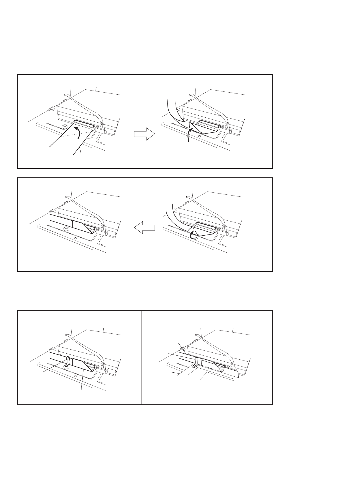
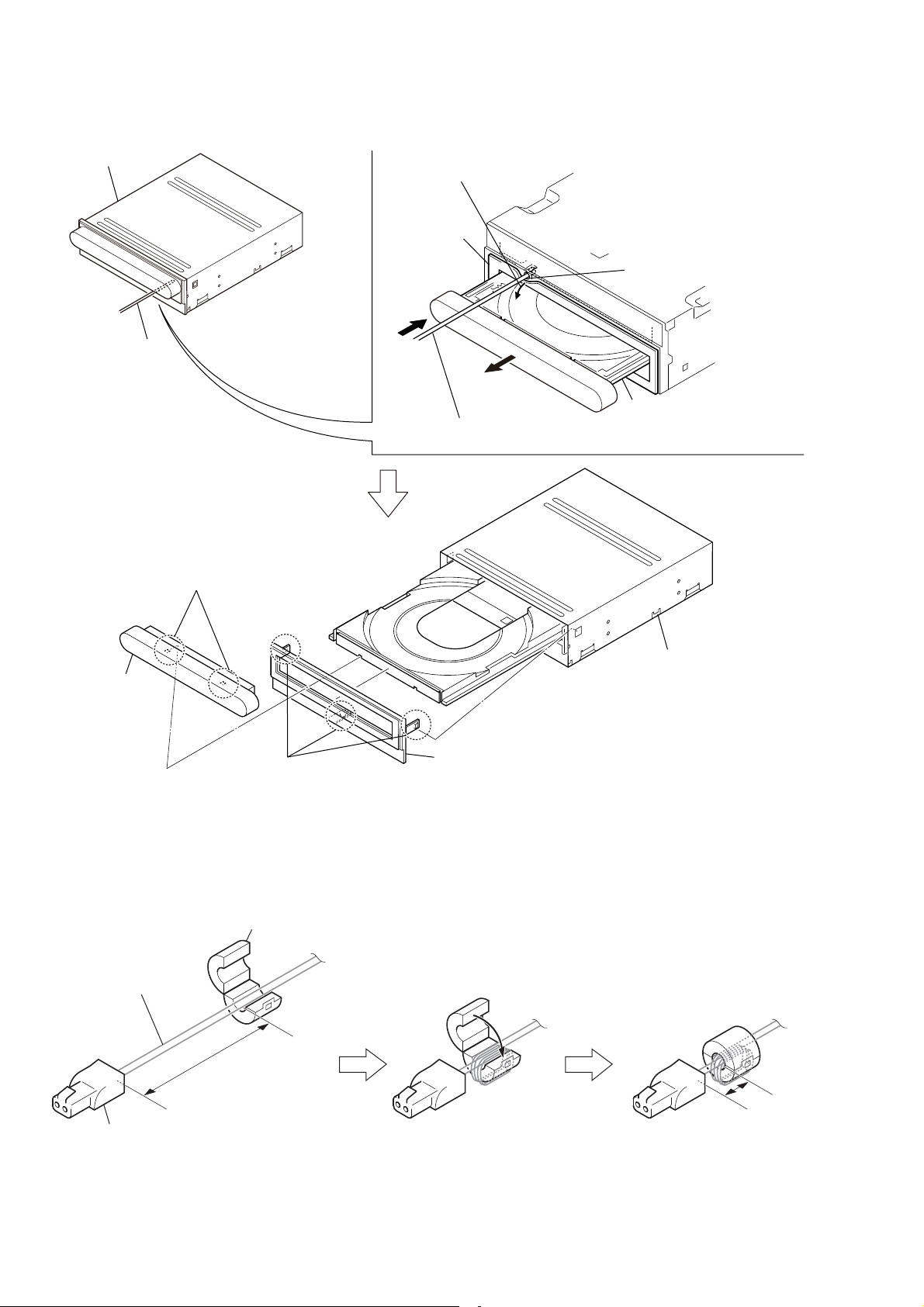
FOLD METHOD OF IDE CABLE
Note: This illustration sees the CD-ROM drive from the back.
1. Fold as the doted IDE cable then fold up as arrow direction in Fig.1.
2. Fold up again as arrow direction in Fig.2.
CD-ROM drive
IDE cable
Fig. 1
Fig. 2
IDE CABLE SETTING
Note: This illustration sees the CD-ROM drive from the back.
Please fi x IDE cable with clamp as shown in the fi gure.
Because there is difference in a fi xation method of IDE cable of AEP and UK MODEL.
(AEP model) (UK model)
CD-ROM drive CD-ROM drive
IDE cable
clamp
clamp
IDE cable
DAB assy
8
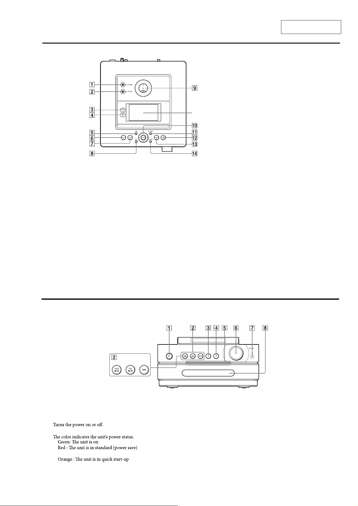
Top of the main unit
AUDIO IN jack
Use to connect the audio output jack of an
external component.
PHONES (headphones) jack
Use to connect headphones.
SERVER indicator
Lights up yellowish green when the unit is
being used as a server and a client device is
playing audio data.
TIMER indicator
Indicates the status of the timer.
SECTION 2
GENERAL
Display
HOME button
Use to select a function from the Home menu.
Press /// to select a function and
press ENTER to enter the selection. To cancel
theHomemenu,pressHOMEorBACK
before pressing ENTER.
PARTY button and indicator
• PA RT Y b ut to n
Use to activate or enter PARTY MODE.
• PARTY indicator
Lights up amber when PARTY MODE is
active.
NAS-S55HDE/SS-S55HDE
This section is extracted
from instruction manual.
x-DJ button
Selects and plays the x-DJ channel.
BACK button
Use to go back to the previous display.
USB port
Use to connect a portable device such as a
USB storage device or the wireless adaptor.
Menu operation buttons
Usetoselectmenuitemsand entermenu
settings.
• ,,andbuttons
Use to select a menu item or to change a
setting.
• ENTER button
Use to enter a setting.
SETTINGS button
Displays the Settings menu. Use to enter
clock, network and other system settings.
HDD REC button
Use for recording to the HDD Jukebox.
TRANSFER button
Use to transfer audio data to a “WALKMAN”
or other portable audio device.
OPTIONS button
DisplaystheOptionsmenu.Menuitemswill
vary according to the selected function.
Front of the main unit
/ (po
wer) button and On/Standby
indicator
• / (power) bu
• On/Standby indicator
—
—
mode.
—
mode or is analyzing music data.
tton
UK model
Function Select buttons
Use to select the function directly. During
standby mode, these buttons turn on the unit
andstartplaybackatthesametime.
• HDD button
• CD button
• FM/AM button (models except the UK
model)
• DAB button (UK model only)
(stop) button
Use in each function to stop an operation.
CD button
Opens and closes the disc tray.
Illumination panel
Lights up when the power is turned on.
Flashes slowly when the unit is analyzing
music data recorded to the HDD Jukebox.
VOLUME dial
Use to adjust the volume.
Remote sensor
Disc tray
Use to load a CD.
9
NAS-S55HDE/SS-S55HDE
Remote control
UK model*
All models except the UK model
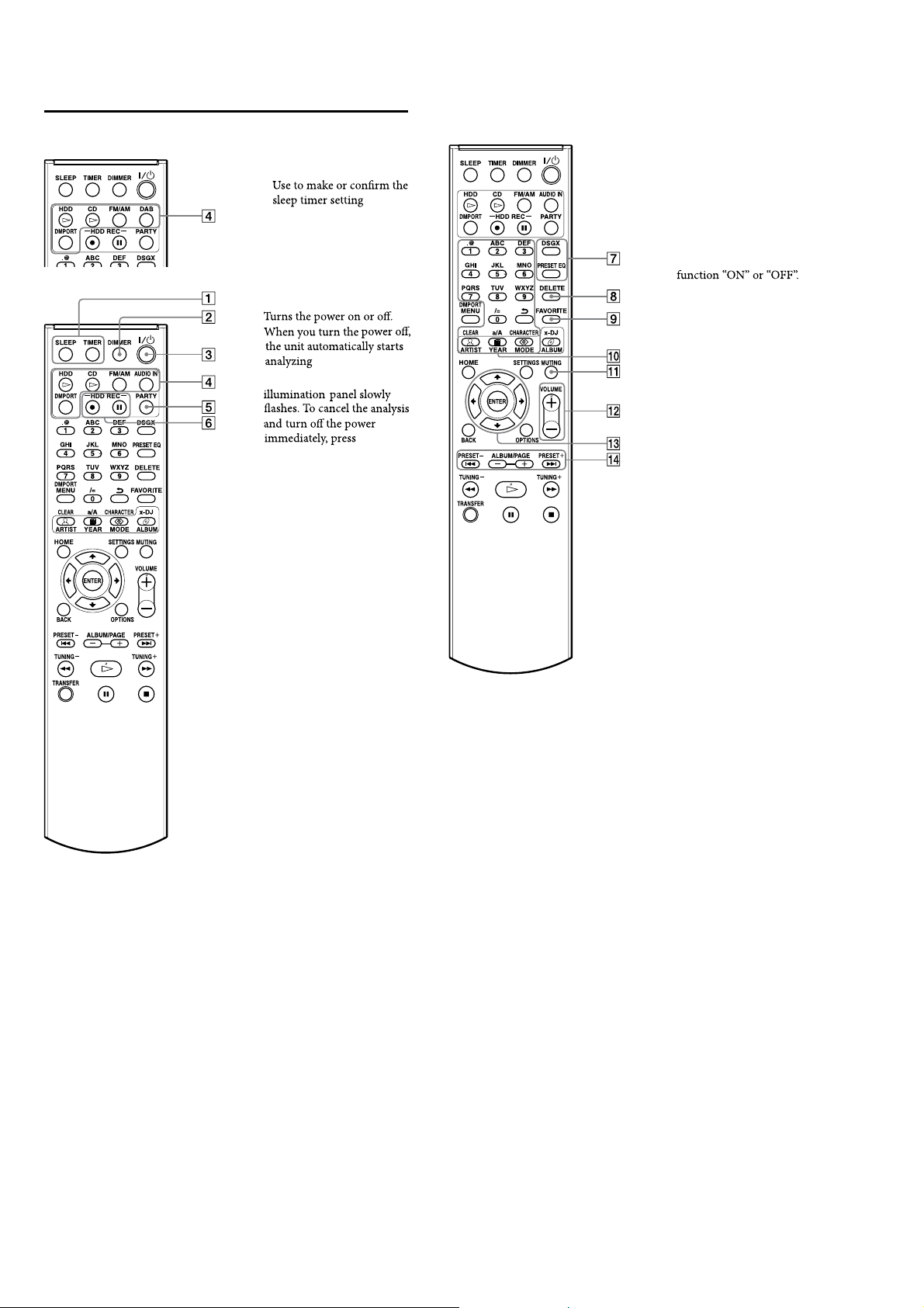
SLEEP and TIMER buttons
SLEEP button
•
TIMER button
•
Use to set the timer.
DIMMER button
Sets the brightness of the
display.
/ (power) button
During this time, the
button.
Function Select buttons*
Usetoselectthefunction
directly. During standby
mode,thesebuttonsturnon
the unit and start playback at
the same time.
HDD button
•
CD button
•
FM/AM button
•
AUDIO IN button (models
•
except the UK model)
DMPORT button
•
DAB button (UK model
•
only)
PARTY button
Use to activate or enter
PARTY MODE.
HDD REC buttons
Use for recording to the HDD
Jukebox.
HDD REC
•
(start recording) button
HDD REC
•
(pause recording) button
* Function Select buttons on the UK
modelperformthesamefunctionas
those with the same name on the
models except the UK model.
music data.
the
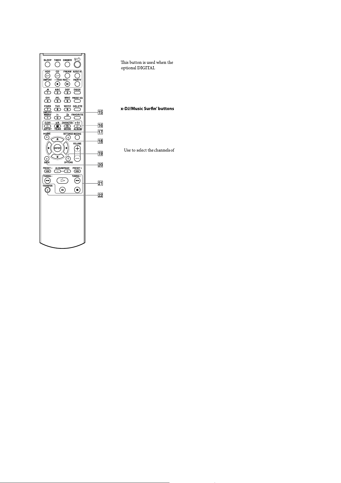
DSGX and PRESET EQ
buttons
.
An asterisk (*) indicates buttons
that have a tactile dot (the number
“5” button and VOLUME + button
of the operation buttons).
• DSGX button
o generate a more
Use t
dynamic sound (Dynamic
Sound Generator X-tra).
Eachpressofthebutton
switches the DSGX
is function is factory set
to “ON”.
• PRESET EQ button
Selects a pre-set customized
sound setting.
Eachpressofthebutton
changes the sound style as
follows.
♦
FLATROCK
POPS JAZZ
CLASSICAL DANCE
FLAT ...
(♦: Factory setting)
DELETE button
Use in each function to delete
an item.
FAVORITE button
Use to add a track to “Favorites”
in the playlist.
Numeric*/text buttons
Use to select a track during
play or to enter text.
MUTING button
Mutes the sound.
VOLUME+* andVOLUME–
buttons
Use to adjust the volume.
Menu operation buttons
Usetoselectmenuitemsand
enter menu settings.
• ,,andbuttons
Use to select a menu item or
to change a setting.
• ENTER button
Use to enter a setting.
• PRESET–, •
PRESET+, ALBUM/PAGE+ •
ALBUM/PAGE– buttons
• andbuttons
Cues the beginning of a track.
• PRESET+ and PRESET–
buttons
Use to select a preset radio
station or DAB service
(UK model only).
• ALBUM/PAGE+ and
ALBUM/PAGE– buttons
Usetoselectanalbumor a
group in the main display.
In a list display, use these
buttonstogotothenext
pageorthepreviouspage.
10
An asterisk (*) indicates buttons
that have a tactile dot (the
(play) button of the operation
buttons).
NAS-S55HDE/SS-S55HDE
DMPORT MENU button
MEDIA PORT adaptor and a
digital media player are
connected. Refer to the
operating manual for the
DIGITAL MEDIA PORT
adaptor.
v x-DJ button (yellow)
Selects and plays the x-DJ
channel.
v ARTIST (blue), YEAR (red),
MOOD (green) and
ALBUM (yellow) buttons
Music Surn’ during x-DJ.
HOME button
Use to select a function from
theHomemenu.
Press /// to select a
function and press ENTER to
enter the selection. To cancel
the Home menu, press
HOME or BACK before
pressing ENTER.
SETTINGS button
Displays the Settings menu.
Useto enterclock,network
and other system settings.
OPTIONS button
Displays the Options menu.
Menu items will vary according
totheselectedfunction.
BACK button
Usetogobacktotheprevious
display.
Operation buttons
Use in all functions to
perform basic operations.
v (play) button*
v (fast rewind) •
TUNING– and
(fast forward) • TUNING
+ buttons
v (pause) button
v (stop) button
TRANSFER button
Use to transfer tracks to a
“WALKMAN” or other
portable audio device.
11
NAS-S55HDE/SS-S55HDE
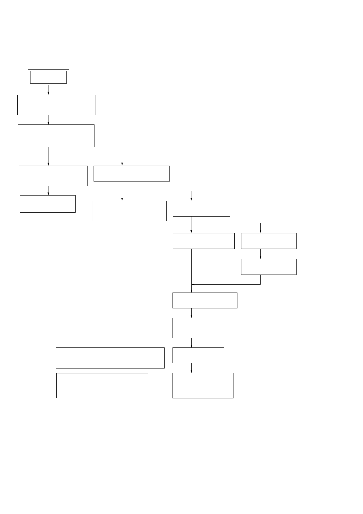
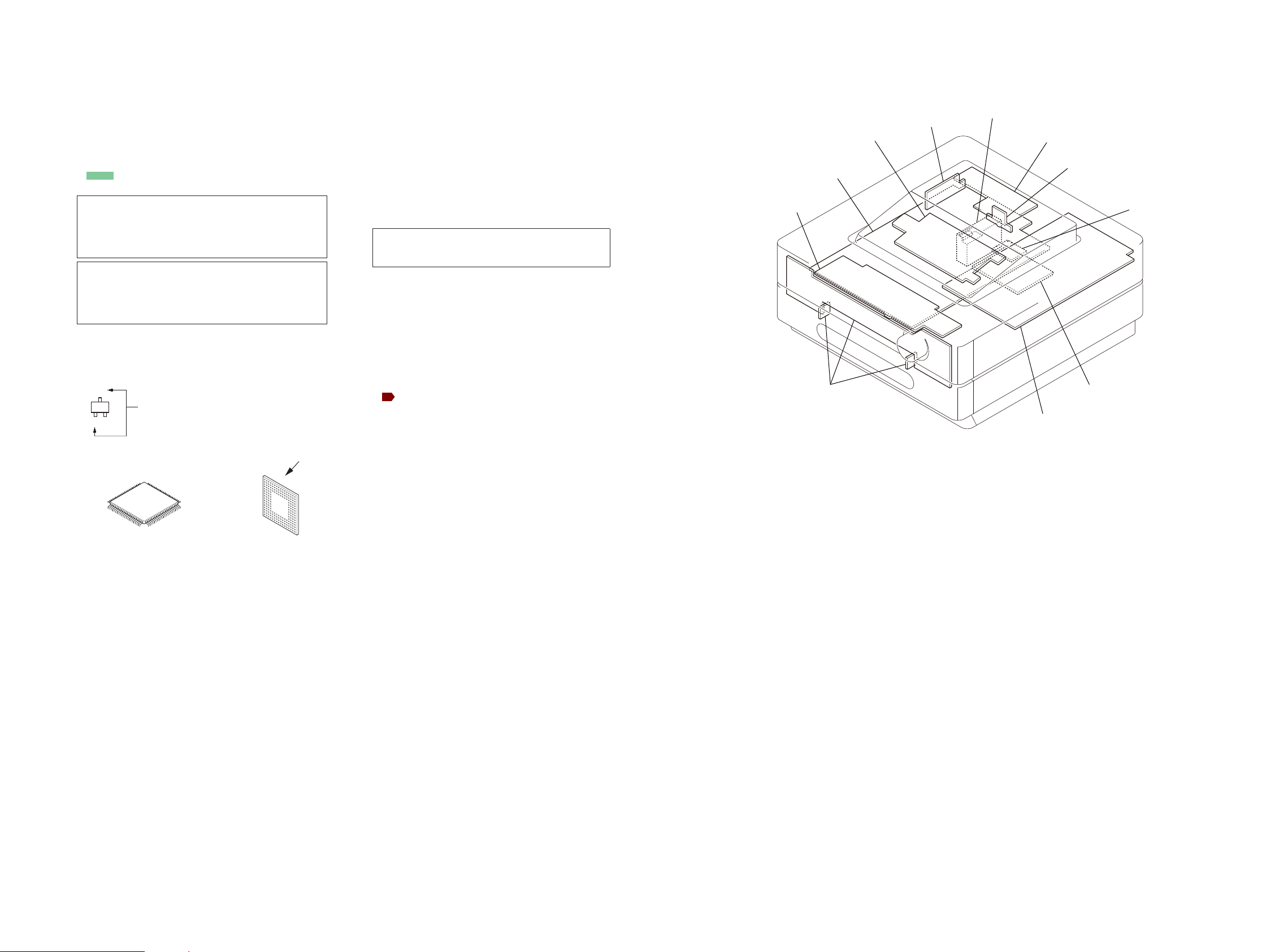
• This set can be disassembled in the order shown below.
3-1. DISASSEMBLY FLOW
SET
3-2. PANEL (SIDE L/R) ASSY
(Page 13)
3-3. COVER (BASE) ASSY,
PANEL (TOP) BLOCK
(Page 13)
SECTION 3
DISASSEMBLY
3-4. PANEL (TOP) BOARD,
LCD BLOCK
(Page 14)
3-5. MODULE (LCD)
(Page 14)
3-6. PANEL (FRONT) BLOCK
(Page 15)
3-7. KNOB (VOL),
PANEL (FRONT) BOARD
(Page 15)
3-8. CHASSIS (TOP)
(Page 16)
3-9. MOTHER BOARD
(Page 16)
3-12. HARD DISC DRIVE
(Page 18)
3-13. FAN. DC (M101),
CHASSIS (MID)
(Page 18)
3-10. SP/DM BOARD
(Page 17)
3-11. MAIN BOARD
(Page 17)
12
3-15. NOTE THE CD-ROM DRIVE AND
INSULATING SHEET (CD) REPLACING
(Page 19)
3-17. POSITION OF FERRITE CORE
FOR SPEAKER CORD
(Page 20)
3-14. CD BLOCK
(Page 19)
3-16. CD-ROM DRAIVE
(CD-5010A-020)
(Page 20)
Note: Follow the disassembly procedure in the numerical order shown below.
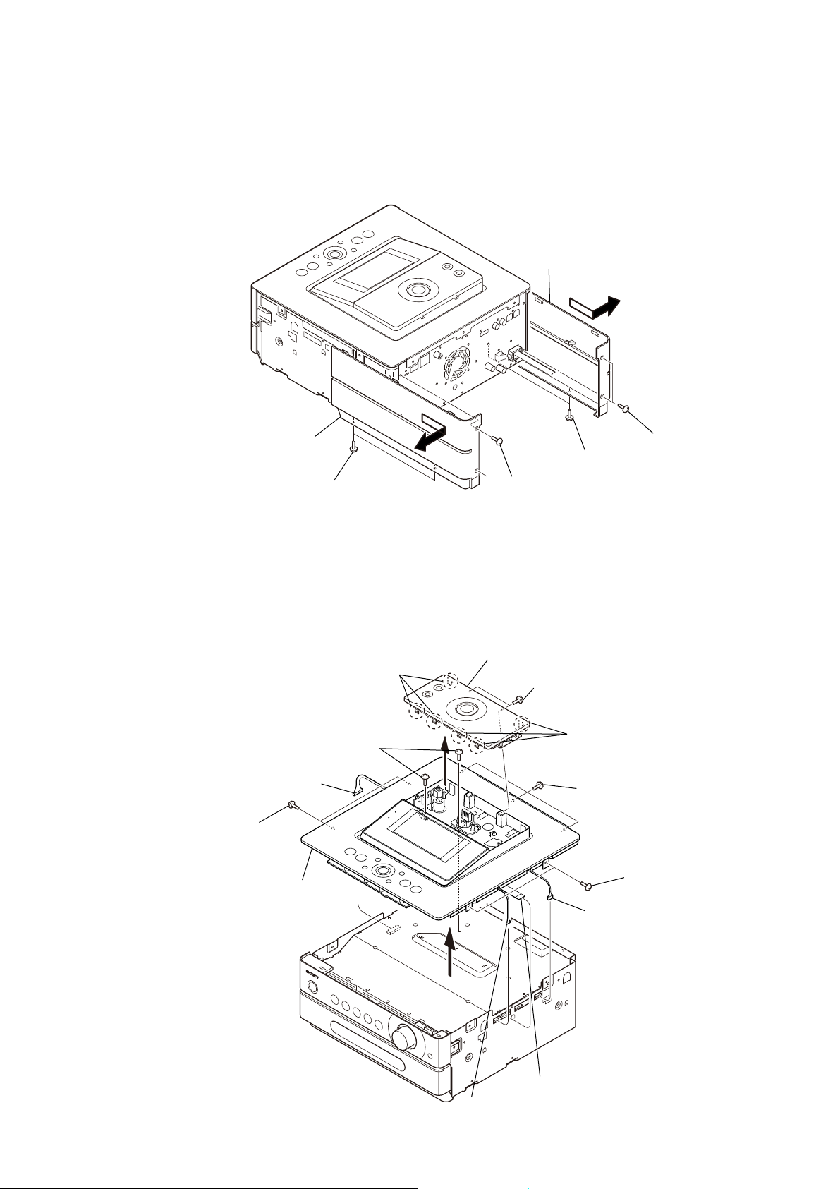
3-2. PANEL (SIDE L/R) ASSY
Note: This illustlation sees the set from back.
NAS-S55HDE/SS-S55HDE
Remove the panel (side L) assy
in the direction of arrow ".
"
Remove the panel (side R) assy
in the direction of arrow #.
two screws
(BVTT3 × 6)
#
3-3. COVER (BASE) ASSY, PANEL (TOP) BLOCK
three claws
two screws
(BV3 × 8)
connector
(CN702)
two screws
R
(BVTP3 × 8)
two screws
(BVTP3 × 8)
cover block assy
two screws
(BVTP3 × 8)
two screws
(BVTT3 × 6)
three claws
three screws
(BVTP3 × 8)
two screws
(BVTP3 × 8)
panel (top) block
RT
RB
connector
(CN852)
R
(BVTP3 × 8)
connector
(CN4002)
flat type wire (15 core)
(CN8)
two screws
13
NAS-S55HDE/SS-S55HDE
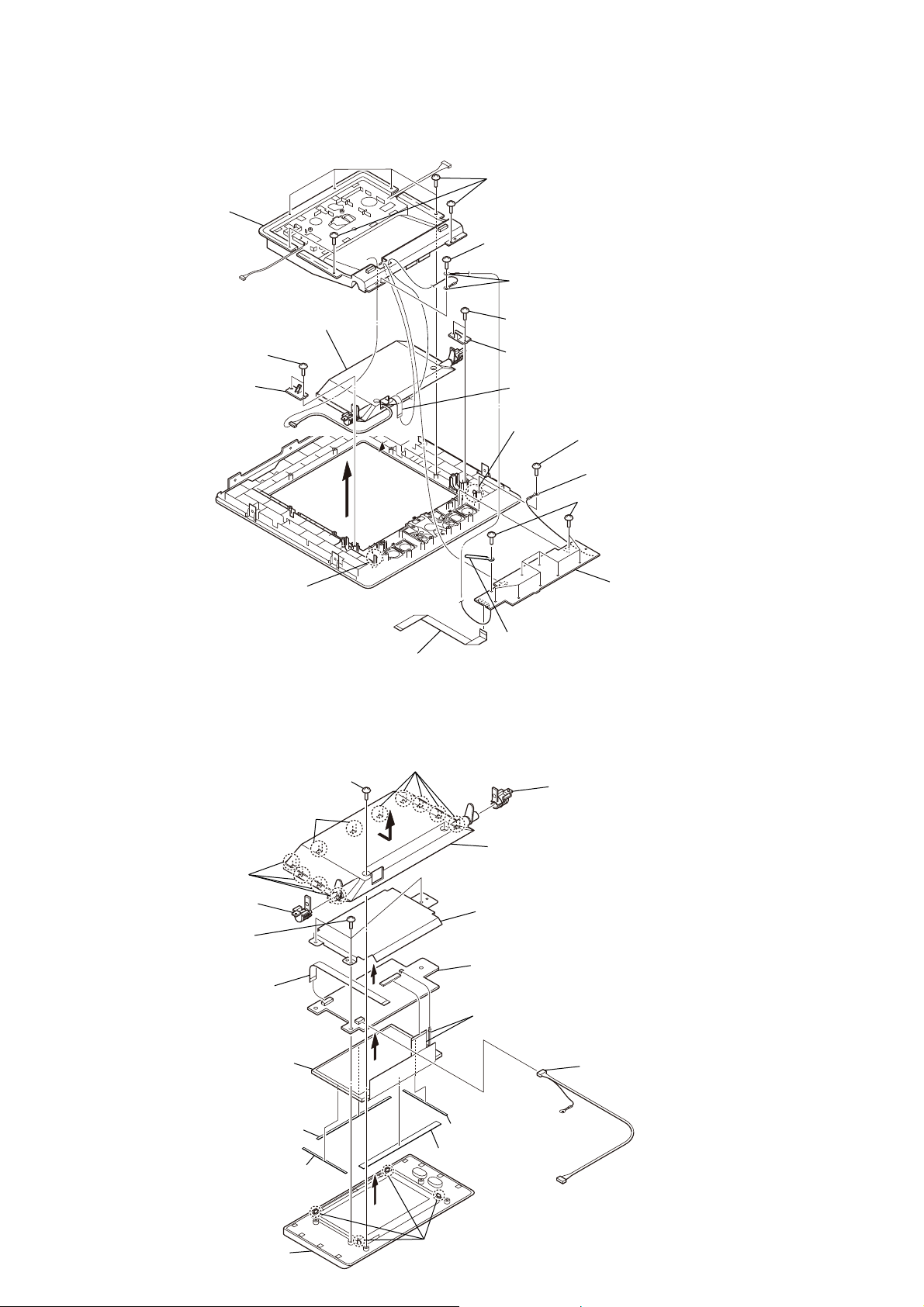
3-4. PANEL (TOP) BOARD, LCD BLOCK
Note: This illustlation sees the panel (top) block from inside.
base (LCD) assy
RT
LCD block
two screws
RH
(BVTP2.6)
RL
seven screws
RB
(BVTP2.6)
screw (BVTP2.6)
two grounds
two screws
RE
(BVTP2.6)
cover (bearing)
RG
cover (bearing)
RI
claw
3-5. MODULE (LCD)
Note: This illustlation sees the LCD block from back.
two screws
(P2.6 × 6)
two claws
four claws
RK
flat type wire (15 core)
(CN850)
five claws
"
flat type wire (9 core)
(CN851)
claw
clamp
Slide the case (LCD B)
in the direction of arrow ".
screw (BVTP3 × 8)
ground
nine screws
(BVTP2.6)
bearing assy
panel (top) board
R
14
bearing assy
three screws
(P2.6 × 6)
flat type wire (9 core)
(CN2503)
LCD module
RI
cushion (LCD)
RE
cushion (LCD)
RG
window (LCD) assy
RT
cushion (LCD)
RG
cushion (LCD)
RH
four claws
RB
shield plate
LCD board
R
LCD module flexible board
(CN2501, CN2502)
cord (with connector)
(CN2504)
3-6. PANEL (FRONT) BLOCK
guround terminal
screw
(BV3 × 8)
panel (front) block
(CN852)
screw
(BVTP3 × 8)
flat type wire (11 core)
(BV3 × 8)
NAS-S55HDE/SS-S55HDE
screw
3-7. KNOB (VOL), PANEL (FRONT) BOARD
Note: This illustlation sees the panel (front) block from inside.
nine screws
(BVTP2.6)
PANEL (FRONT) board
two claws
two screws
(BVTP3 × 8)
knob (VOL)
string
Note: String is hung on the root of knob (VOL), string is pulled
and knob (VOL) is removed as shown in the figure.
15
NAS-S55HDE/SS-S55HDE
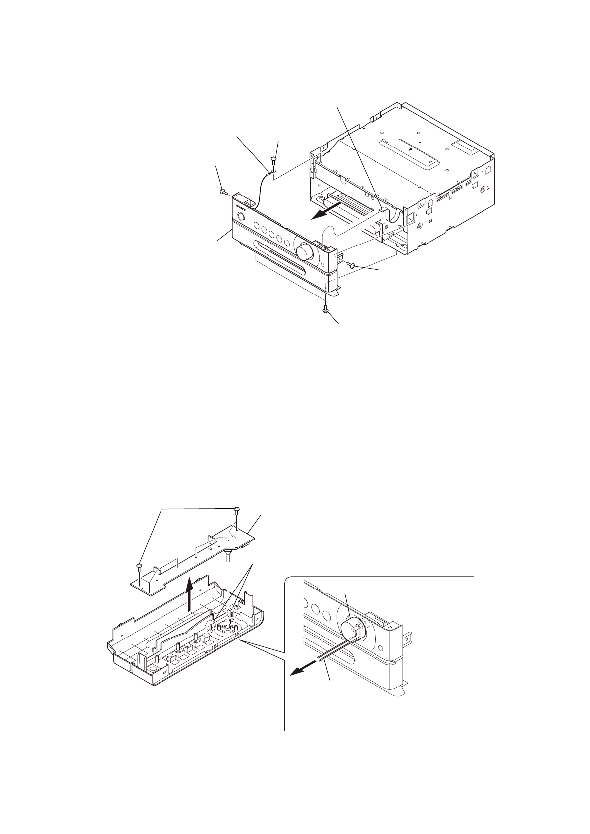
3-8. CHASSIS (TOP)
three screws
(BVTP3 × 8)
three screws
(BVTP3 × 8)
chassis (top)
screw
(BVTP3 × 8)
3-9. MOTHER BOARD
two connectors
(CN1, CN12)
two screws
(BV3 × 8)
three screws
(BVTP3 × 8)
MOTHER board
R
screw
(PWH3 × 8)
flat type wire (11 core)
(CN510)
flat type wire (7 core)
(CN9201)
screw
(BVTT3 × 8)
connector
(CN7)
16
(CN512)
flat type wire (19 core)
(CN513)
flat type wire (5 core)
3-10. SP/DM BOARD
two screws
(BVTP3 × 8)
heat sink
radiation sheeh
ferrite core
SP/DM board
three screws
(BVTP3 × 8)
flat type wire (11 core)
(CN6100)
NAS-S55HDE/SS-S55HDE
(CN6102)
3-11. MAIN BOARD
four screws
RB
(BVTP3 × 8)
power cord connector
R
(CN201)
connector
MAIN board
RG
screw
RT
(BVTP3 × 8)
RE
clamp
flat type wire (11 core)
(CN110)
two connectors
(CN1, CN851)
two connectors
(CN108, CN110)
flat type wire (9 core)
(CN102) (UK model)
flat type wire (11 core)
(CN114)
flat type wire (15 core)
(CN141)
flat type wire (15 core)
(CN701)
flat type wire (7 core)
(CN109)
flat type wire (11 core)
(CN112)
17
NAS-S55HDE/SS-S55HDE
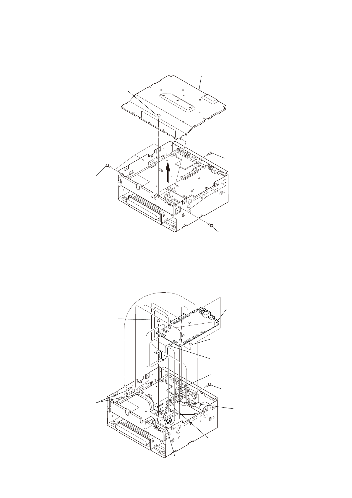
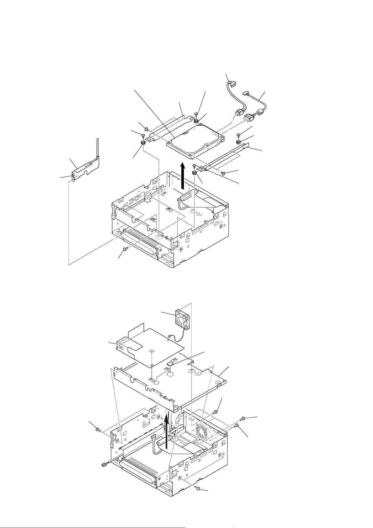
3-12. HARD DISC DRIVE
hard disc drive
RE
two screws
(6-32UNCX5)
HDD damper screw
chassis (mother)
claw
damper
HDD damper screw
chassis (HDD-L)
harness
RT
(serial ATA)
damper
damper
harness
RB
(for SATA power)
HDD damper screw
damper
chassis (HDD-R)
R
two screws
(6-32UNCX5)
HDD damper screw
screw
(BVTP3 × 8)
3-13. FAN. DC (M101), CHASSIS (MID)
sheet (insulating)
two screws
(PTP3 × 8BT)
fan, (DC)
(M101)
two radiation sheets (S)
chassis (MID)
two screws
(BVTP3 × 8)
(BVTP3 × 8)
screw
(PTP3 × 8BT)
three screws
18
two screws
(PTP3 × 8BT)
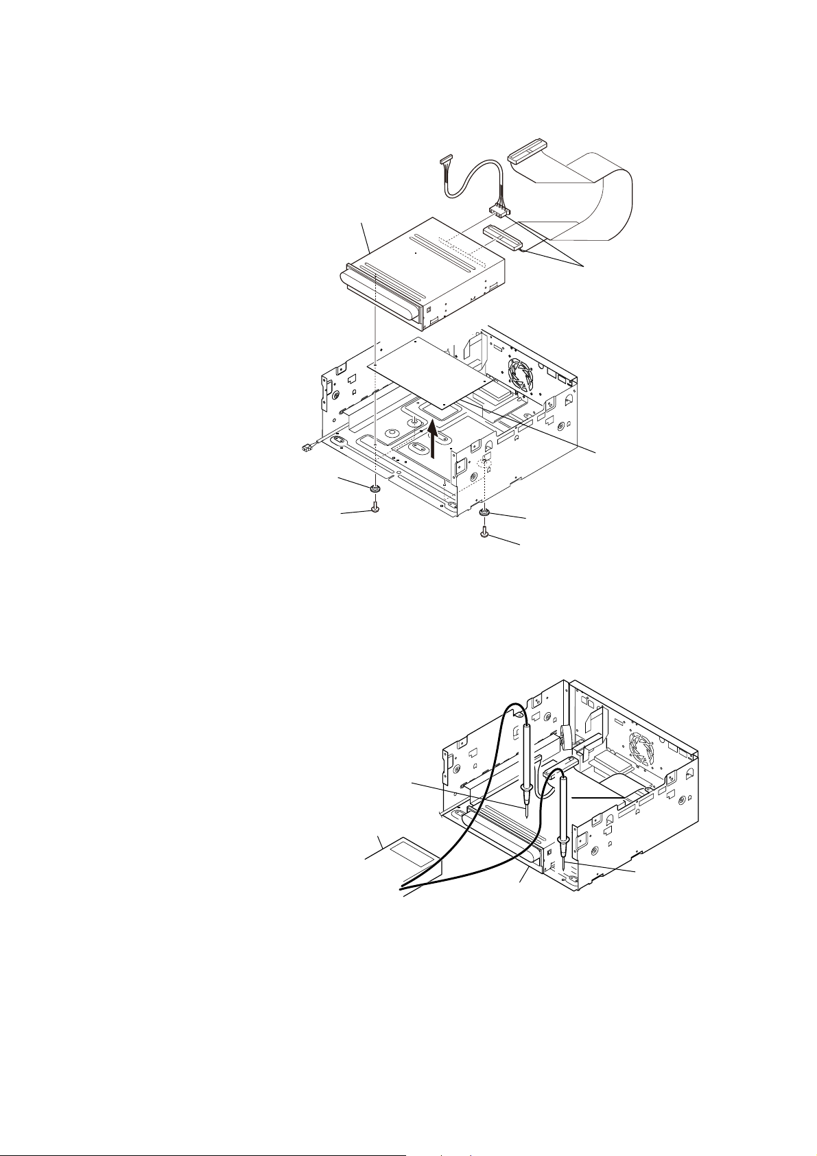
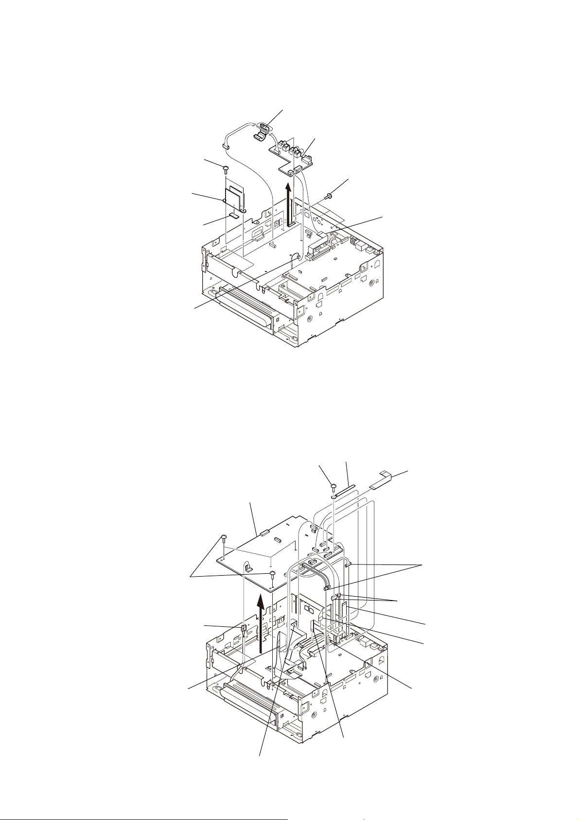
3-14. CD BLOCK
Note: When installing a CD block,
please confirm the watch to have
bushing (insulating) (4 pcs) by the
last process.
CD block
NAS-S55HDE/SS-S55HDE
two connectors
two bushings (insulating)
two screws
(BVTT3 × 6)
two bushings (insulating)
two screws
(BVTT3 × 6)
3-15. NOTE THE CD-ROM DRIVE AND INSULATING SHEET (CD) REPLACING
When replacing the insulating sheet (CD) or CD-ROM drive,
be sure to confirm that a CD-ROM drive and
chassis (base) do not conduct electricity with a tester.
CD-ROM drive
(upper face)
tester
F
&
insulating sheet (CD)
CD-ROM drive
chassis (base) assy
(bottomface)
19
NAS-S55HDE/SS-S55HDE
3-16. CD-ROM DRIVE (CD-5010A-020)
CD block
thin rod
two claws
Peel the cushion (CD) a
little when it hides the hole.
cushion (CD)
"
Insert a thin rod into the hole and push it in the
arrow " direction. (Disc tray will come out)
Note: This illustration shows the
disc tray as viewed from
the bottom.
hole
disc tray
panel (CD-L)
bezel assy
three claws
3-17. POSITION OF FERRITE CORE FOR SPEAKER CORD
sleeve ferrite clamp
Pull out the cord
with connector (speaker).
150 mm
cord with connector (speaker)
Wrap in 2 turn as
diagram then lock it.
CD-ROM drive
(CD-5010A-020)
Make 2 set.
15 ± 5 mm
20

SECTION 4
TEST MODE
CD BOOT MODE
Procedure:
1. The power supply code is inserted in the outlet with the [Z]
button pushed.
2. The boot disk is put on the disk tray within 30 seconds because
the disk tray comes out. Do over again from step 1 when 30
seconds or more pass.
3. CD boot mode starts when the boot disk is recognized.
SH IPL DIAG MODE + LINUX DIAG MODE
Procedure:
1. The power supply code is inserted in the outlet with the [x-DJ]
and [TRANSFER] buttons pushed.
2. SH IPL DIAG mode starts.
INSTANTLY RESTORATION MODE
Procedure:
1. The power supply code is inserted in the outlet with the
[PARTY], [HOME] and [M] buttons pushed.
2. Instantly restoration mode starts.
NAS-S55HDE/SS-S55HDE
21

NAS-S55HDE/SS-S55HDE
MEMO
22
NAS-S55HDE/SS-S55HDE
NAS-S55HDE/SS-S55HDE
2323
HD0− HD15
• SIGNAL PATH
:USB
: HDD
:LAN
:VIDEO
: CD PLAY
:AUDIO
D
ETHERNET INTERFACE
IC3001
5RX+
6RX
−
1TX
+
2TX
−
J2
NETWORK
5
2
1
RD+
RD
−
TD+
6
8 CTRL25
108 EEDO
109 AUX/EEDI
111 EESK
106 EECS
+3.3V+2.5V
TD
−
EEPROM
IC3002
+2.5V
REGULATOR
Q3001
PAR
76
SERRB
75
PERRB
70
STOPB
69
DEVSELB
68
TRDYB 67
IRADYB
63
FRAMEB
61
CBEB2
60
CBEB3
44
PCIRSTB
27
INTAB
AD0− AD31
25
CBEB0
92
CBEB1
PAR
XSERR
XPERR
XSTOP
XDEVSEL
XTRDY
XIRDY
XFRAME
XCBE2
XCBE3
XPCIRST
XINTB
XCBE0
XCBE1
77
AD0− AD31
IDSEL
46
AD21
GNTB
29
REQB
XGNT1
XREQ1
30
PCICLK 28
XTAL1
121
USB INTERFACE
IC4001
114 DP1
112 DM1
J3
(USB)
2
3
USB D1+
USB D1
−
135 DP4
133 DM4
J4800
(USB)
2
3
USB D4+
USB D4
−
52
53
48
49
33
16
24
23
20
21
22
AD0− AD31
60
50
XDEVSEL
XSTOP
XCBE2
XFRAME
XCBE3
XPCIRST
XREQ2
XGNT2
XINTA
XINTB
XINTC
XCBE1
XIRDY
XTRDY
51
AD0− AD31
AD23
59
69
58
PAR
XCBE0
XSERR
XPERR
DEVSEL0
STOP0
CBE20
FRAME0
CBE30
VBBRST0
REQ0
GNT0
INTA0
INTB0
INTC0
CBE10
IRDY0
TRDY0
PAR
CBE00
34
IDSEL
SERR0
PERR0
57
PCLK
15
XT1/SCLK 95
AUDIO DSP INTERFACE
IC9101
54
124
7
93
94
123
78
9
56
58
XTRDY
XSTOP
XIRDY
XDEVSEL
XPERR
XFRAME
XINTA
PAR
XCBE1
XCBE0
XSERR
125
6
118
85
XCBE2
XREQ0
XGNT0
XCBE3
XTRDY
XSTOP
XIRDY
XDEVSEL
XPERR
XFRAME
INTA
PAR
XCBE1
XCBE0
XSERR
XCBE2
XREQ0
XGNT0
XCBE3
49
43
XPCIRST
XPCIRST
79
RST
DSPRST#
HD0− HD15
DSP_BUS
XTRDY
XSTOP
XIRDY
XDEVSEL
XPERR
XFRAME
XINTA
PAR
XCBE2
XCBE3
XSERR
XCBE1
XREQ0
XGNT0
XCBE0
XPCIRST
PCICLK
117
AD0− AD31
AD0− AD31 HD0− HD15
AND GATE
IC9102
112
35
71
106
HDS2#
HDS1#
HCNTL1
HR/W#
HCS#
36
28
39
38
HCNTL0
HINT#
HRDY#
HHWIL
HDS2#
HDS1#
HCNTL1
HR/W#
HCS#
HCNTL0
HINT#
HRDY#
HHWIL
105
DD0− DD15 DD0− DD15
B
C
CPU
IC1001 (1/2)
187
206
168
167
185
188
23
205
149
122
204
203
46
69
XTRDY
XSTOP
XIRDY
XDEVSEL
XPERR
XFRAME
XINTA
XINTB
315
XINTB
XINTC
338
XINTC
PAR
XCBE2
XCBE3
XSERR
XCBE1
XREQ0
XREQ1
45
XREQ1
XREQ2
68
XREQ2
XGNT0
XCBE0
260
XGNT1
92
XGNT1
XGNT2
91
XGNT2
25
XPCIRST
PCICLKOUT
4825MHz-ASIC
XPOR
DPSCLK
377
AD0− AD31
AD0− AD31 DD0− DD15
349
350
326
327
348
325
324
347
XDIOR
DMARQ
IORDY
XDIOW
XDMACK
346
391
356
XCS0
XCS1
IDERST
382
403
402
DAC
DAY
DACVBS
DAC
DAY
DACVBS
INTRQ
DA0
DA1
DA2
XDIOR
DMARQ
IORDY
XDIOW
XDMACK
XCS0
XCS1
361
PA3
XSATARESET
IDERST
INTRQ
DA0
DA1
DA2
370
XDIOR
DMARQ
IORDY
XDIOW
XDMACK
XCS1
XCS0
IDERST
INTRQ
DA1
DA2
X1001
25MHz
XTAL
EXTAL
378
400
7
D
CLOCK GENERATOR
IC1701
9
B
10
A
8
E
1
C
X1701
27MHz
XOUT
XIN
5
4
DD0− DD15
XDIOR
DMARQ
IORDY
XDIOW
XDMACK
XCS0
IDERST
INTRQ
DA1
DA0
DA0
DA2
CD-
ROM
DRIVE
4
3
2
1
DO
DI
CLK
CS
385SDA
384SCL
EEPROM
IC1002
5
6
SDA
SCL
SYSTEM CONTROLLER
IC501 (1/3)
XRESUME
51
MOTHER_PA0
49
MOTHER_PA5
48
STATUS
50
XPOR (COURGER)
52
UART_OUT
31
UART_IN
32
AUDCK
321
PA0
278
PA5
295
PA6
287
RESET
398
PA2
318
PA1
339
HARD
DISK
DRIVE
HDD DRIVER
IC5001
23
XTLOUT22XTLIN/OSC
X5001
25MHz
27RX_P
28RX_M
32TX_P
31TX_M
H_DD0 –
H_DD15
54 H_DMACK_N
58 H_DIOR_N
48 H_CS_0
47 H_CS_1
49 H_DA2
50 H_DA0
51 H_DA1
59 H_DIOW_N
H_INTRQ
60 H_DMARQ
55 H_IORDY
53
16 H_RESET_N
17 RST_N
SECTION 5
DIAGRAMS
5-1. BLOCK DIAGRAM - MAIN Section -
(Page 24)
(Page 24)
(Page 24)
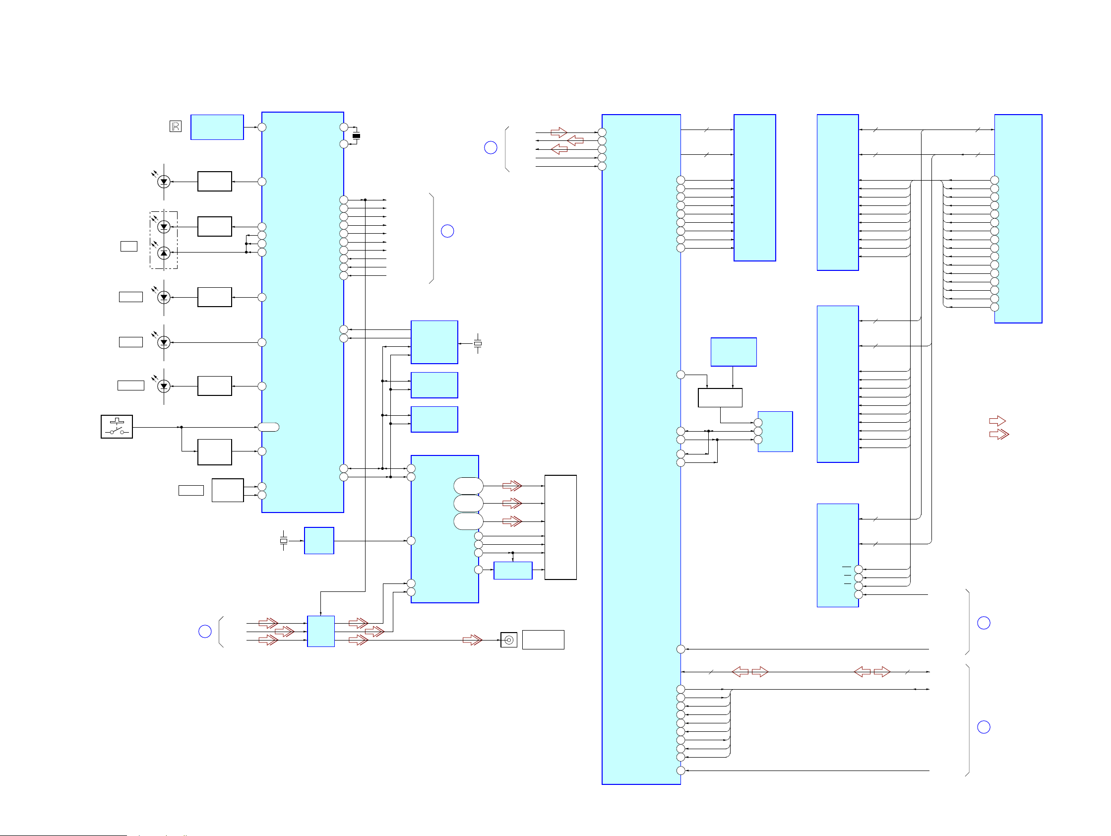
NAS-S55HDE/SS-S55HDE
NAS-S55HDE/SS-S55HDE
2424
5-2. BLOCK DIAGRAM - PANEL, DSP Section -
HD0− HD15 HD0− HD15
• SIGNAL PATH
:AUDIO
D
C
AUDIO DSP
IC9201
A13
DSPRST#
DSPRST#
HD0− HD15
DSP_BUS
A3
CLKIN
25MHz-ASIC
XPOR
CPU
IC1001 (2/2)
217
218
219
220
35
13
36
14
21
355
DQMUU
DQMLU
DQMUL
DQMLL
DQM64UU
DQM64LU
DQM64UL
DQM64LL
XCS1
XRD
CKE
66
334
87
86
XCS0
XWE
XCAS
XRAS
65
44
CLK
DQMUU
DQMLU
DQMUL
DQMLL
DQM64UU
DQM64LU
DQM64UL
DQM64LL
XCS1
XRD
CKE
XCS0
XWE
XCAS
XRAS
CLKOUT
D0− D63
D0− D63
A0− A18
A0− A18
HD0− HD15
F18
E19
G19
G20
HDS2#
HDS1#
HCNTL1
HR/W#
HCS#
F20
G18
J20
H19
HCNTL0
HINT#
HRDY#
HHWIL
HDS2#
HDS1#
HCNTL1
HR/W#
HCS#
HCNTL0
HINT#
HRDY#
HHWIL
H20
V5
Y10
W10
Y4
U19
N2
N1
C2
V17
V11
V12
V20
DQMUU
DQMLU
DQMUL
DQMLL
CKE
XCS1
XWE
XCAS
XRAS
CLK
D0− D31
A0− A11,
A13, A14
SD-RAM
IC2001
D0− D31
A0− A11,
BS0, BS1
ED0− ED31
EA2− EA15
SD-RAM
IC9301
DM2
DM1
DM3
CLK
RAS
CS#
CAS
WE#
DM0
BE2#
BE1#
BE3#
ECLKOUT
SDRAS#
CE0#
SDCAS#
SDWE#
BE0#
D0− D31
A0− A11,
BS0, BS1
ED0− ED31
EA2− EA15
DQM64UU
DQM64LU
DQM64UL
DQM64LL
CKE
XCS1
XWE
XCAS
XRAS
CLK
D32− D63
A0− A11,
A13, A14
SD-RAM
IC2101
D0− D31
A0− A11,
BS0, BS1
XWE
XCS0
XRD
D0− D15
A1− A18
FLASH MEMORY
IC2201
RST#
WE
CE
OE
DQ0− DQ15
A0− A17
11
26
28
12
LCD-POWER
BL1
BL2
A
ENC_A/SEL_A
ENC_B/SEL_B
VOLUME
I/
PARTY
68
69
SIRCS
18
KEY_INT
19
KEY_A0 – KEY_A3
LED_ILLUMI
26
ROTARY
ENCODER
S879
S850 – 861, 867,
S869, 870, 872 – 875
SYSTEM CONTROLLER
IC501 (2/3)
55LCD_BL2
54LCD_BL1
53LCD_CNT_POW
LCD
MODULE
LED DRIVE
Q508, 510
REMOTE CONTROL
RECEIVER
IC851
D856, 857
(ILLUMINATION)
LED_ANY
81
LED DRIVE
Q512
D850
TIMER
LED_TIMER
79
D2601
SERVER
LED_SERVER
100
D2602
LED_PON
80
LED_STBY2
5
LED_STBY1
4
LED_STBY0
3
AXRO-2
G1
AXRO-4
F1
ACLKXO
G3
AFSXO
H1
AXRO-1
H2
LED DRIVE
Q505
KEY ACTIVE
SWITCH
Q501
D859
86 – 83
LED DRIVE
Q513
DAC
DAY
DACVBS
29I2C_CLK
30I2C_DATA
12XRST
74RTC_INT
POWER_ON
FAN_ON
AC_CUT
87AC_CUT
82FAN_ON
70POWER_ON
DAB_1.2V
DAB_3.3V
34DAB_3.3V
33DAB_1.2V
AU-EMERG
75AU-EMERG
EMERGENCY
73EMERGENCY
B
REAL TIME
CLOCK
IC502
X502
32.768kHz
TEMPERATURE
SENSOR
IC503
TEMPERATURE
SENSOR
IC2601
LCD CONTROLLER
IC2501
VIDEO
AMP
IC1401
J1
MONITOR OUT
(NTSC)
X2501
32MHz
SDA
SCL
168
169
REFCLK
166
VIN3
VIN6
21
31
CLOCK
BUFFER
IC2510
DR0 – DR7
DG0 – DG7
DB0 – DB7
66CP
71LCP
72FRP
68DISP
D FLIP-FLOP
IC2507
:VIDEO
74 – 77,
79 – 82
56 – 59,
61 – 64
46 – 49,
51 – 54
SDO1
SDO2
SDI
BCK1
LRCK1
EEPROM
IC9401
RESET SWITCH
Q9401, 9402
SDA
5
WP
7
SCL
6
SCL
SDA
WP
D2
C1
SCL
SDA
E
RESET SIGNAL
GENERATOR
IC9402
X501
16MHz
XOUT
XIN
13
15
DM2
DM3
DM0
DM1
CKE
CS#
WE#
CAS
RAS
CLK
DM2
DM3
DM0
DM1
CKE
CS#
WE#
CAS
RAS
CLK
(Page 25)
(Page 26)
(Page 23)
(Page 23)
(Page 23)
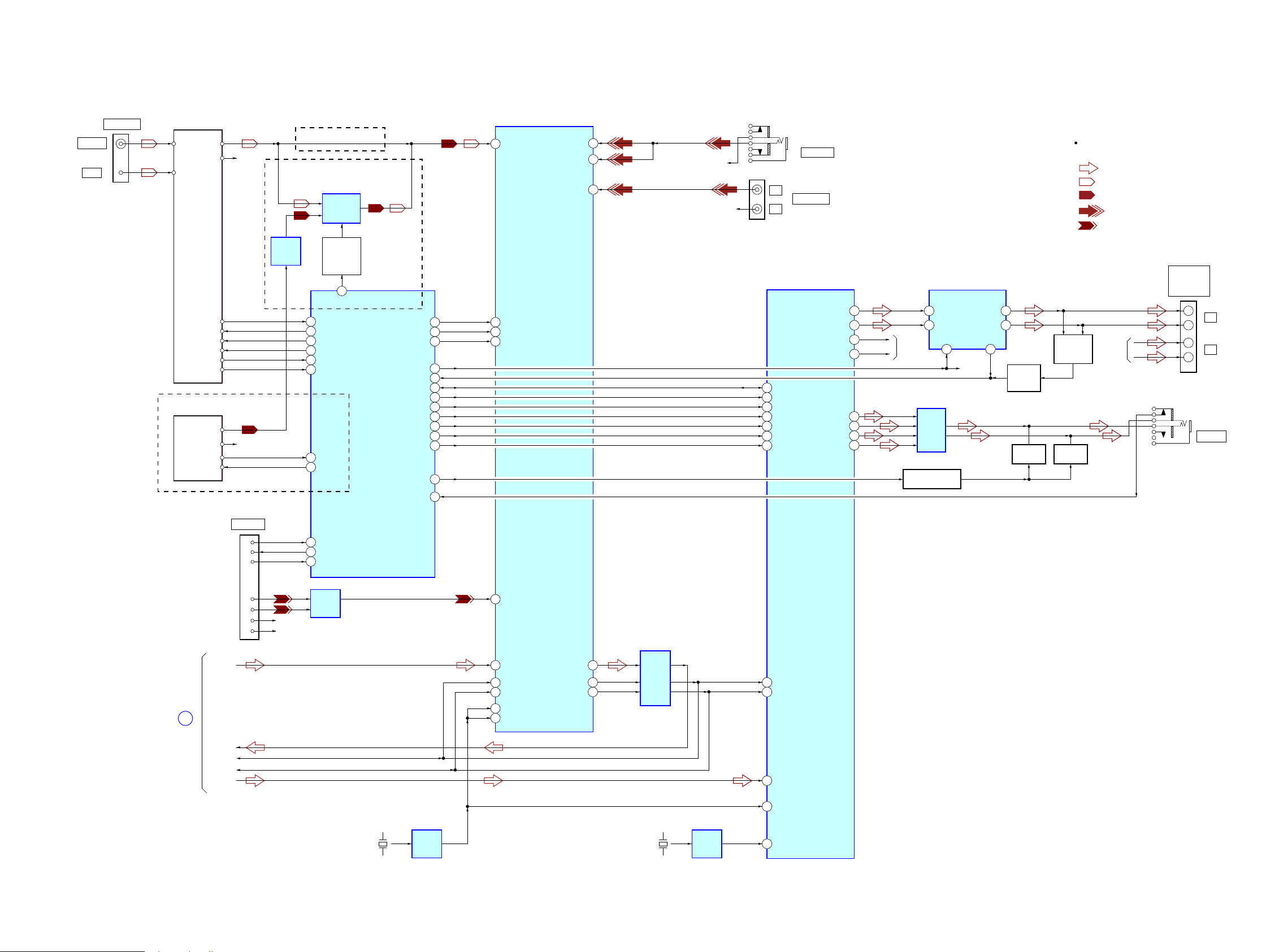
NAS-S55HDE/SS-S55HDE
NAS-S55HDE/SS-S55HDE
2525
5-3. BLOCK DIAGRAM - AUDIO Section -
R-CH
CLOCK
BUFER
IC104
X101
11.289MHz
AIN3L
47
AIN5L
43
INPUT SELECT, D/A CONVERTER, A/D CONVERTER
IC102
SYSTEM CONTROLLER
IC501 (3/3)
• SIGNAL PATH
:DMPORT
:AUDIO IN
: TUNER
:DAB
:AUDIO
R-ch is omitted due to same as L-ch.
DIN
6
AIN4L
45
AIN2L
1
AIN1L
3
TUNER (FM/AM)
J6100
AM
L
R
L
R
ANTENNA
FM ANT
AM ANT
LCH
RCH
DO/STEREO
R-CH
R-CH
R-CH
DI
CL
CE
FM 75Ω
J460
23 TU_DI
24 TU_DO
6
TUNER/DAB
DAB TUNER MODULE
AUDL
AUDR
S1_DOUT
R-CH
S1_DIN
36 DAB_RXD
35 DAB_TXD
22 TU_CLK
25 TU_CE
RDS_DATA
RDS_CLK
21 RDS_DATA
20 RDS_CLK
AUDIO IN
DI
18
CL
19
4DACBCLK
12DOUT
7DACLRC
CE
17
SDO2
SDO1
SDI
BCK1
LRCK1
ADCMCLK
11
DACMCLK
5
ADCLRC
13
ADCBCLK
10
E
CLOCK
BUFER
IC703
X702
49.152MHz
BUFFER
IC103
DIGITAL POWER AMP
IC704
J464
SPEAKER
IMPEDANCE
USE 6Ω
31
11
DATA
OUTL1
9OUTL2
6OUTR1
4OUTR2
OVER LOAD
DETECT
Q707, 709
DAB/TUNER
SELECT
CONTROL
Q106
STREAM PROCESSOR
IC702
4 PWM_A OUT_A
6
5
PWM_B
/RST_AB
3
/SD
36 XFSIIN
48 XFSOIN
30
BCK
29
LRCK
HPOUTL1
HPOUTL2
HPOUTR1
HPOUTR2
21 SCDT
22 SCSHIFT
23 SCLATCH
27 INIT
19 SOFTMUTE
R-CH
33
OUT_B
30
+
–
R-CH
PHONES
J462
45
43
41
39
LINE
AMP
IC706
DAB/TUNER
SELECT
IC109
MUTING CONTROL
Q504
MUTING
Q702, 705
PROTECT
DETECT
Q706
MUTING
Q701, 704
+
–
45
44
43
37
39
18 NSPMUTE
20 PGMUTE
S-MASTER_DATA
S-MASTER_SHIFT
40
47
S-MASTER_RST
S-MASTER_SD
S-MASTER_LAT
S-MASTER_INIT
S-MASTER_SOFT_MUTE
S-MASTER_NSP
S-MASTER_PG_MUTE
42
38
HP_MUTE
HP_IN
61
63
58AU_DO
57AU_CLK
56AU_CE
AUDIO IN
CN6101
DMPORT
(AEP)
(UK)
(UK)
6
5
7
DET
RXD
TXD
12
R- R-CH
14
R+ R-CH
11
L-
13
L+
76 DETECT
77 TXD6
78 RXD6
LINE
AMP
IC6101
LINE
AMP
IC403
(Page 24)
NAS-S55HDE/SS-S55HDE
NAS-S55HDE/SS-S55HDE
2626
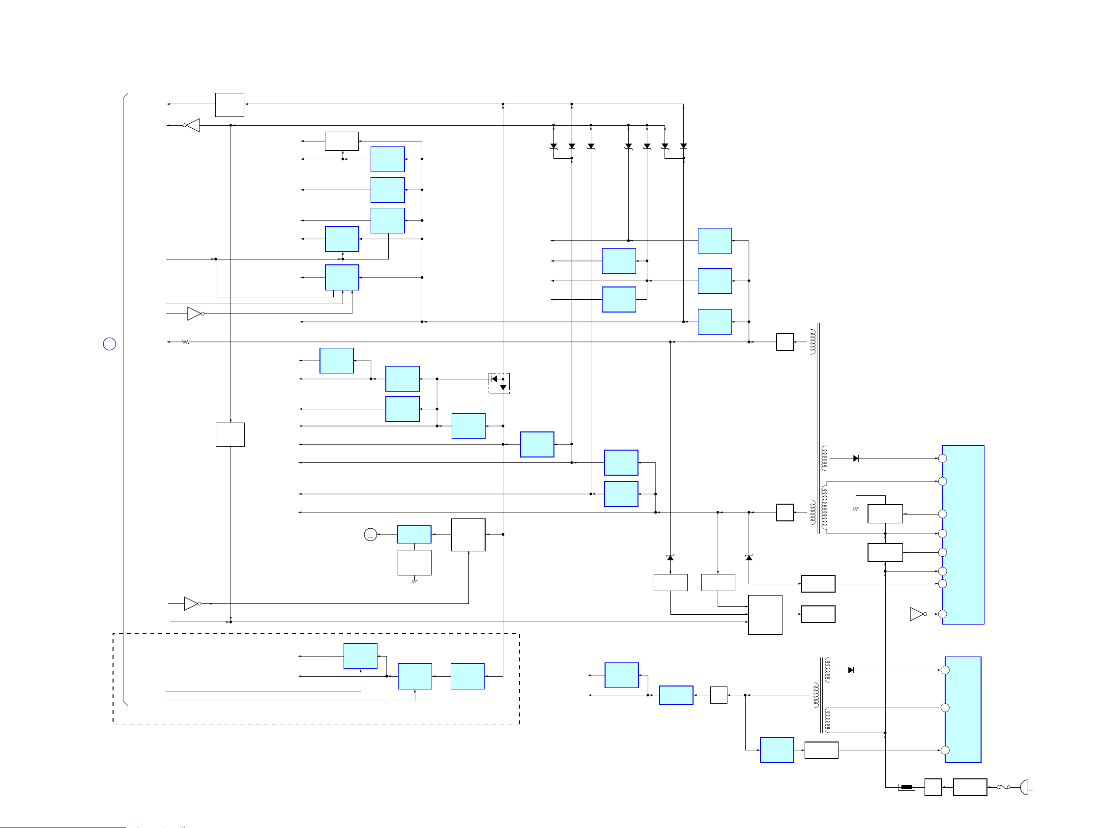
5-4. BLOCK DIAGRAM - POWER SUPPLEY Section -
POWER CONTROL
IC202
D213
D206
+3.3VSB
(AC IN)
F201
LINE FILTER
T201
RECT
D201
TH201
22 VS
24 VD
1 VSENSE
2 F/B
23 VG (H)
20 VG (L)
15 VC1
POWERCONTROL
IC201
5 DRAIN
2FB
4VCC
ISOLATOR
PC204
ISOLATOR
PC203
ISOLATOR
PC201
T203
SUB POWER
TRANSFORMER
T202
MAIN POWER
TRANSFORMER
RECT
D316
CPU +1.2V
POWER
ON/OFF
CONTROL
SWITCH
Q302
SWITCHING
Q202
SWITCHING
Q201
SHUNT
REGULATOR
IC301
REGULATOR
IC307
RECT
D303
RECT
D302
AMP VCC
D306
LCD-POWER
+3.2V
REGULATOR
IC2504
LCD A +3.2V
LCD BACKLIGHT B+
LCD D +3.2V
+3.2V
REGULATOR
IC2508
BL1
Q851
LED
DRICER
IC851
BL2
DAB_1.2V
DAB_3.3V
LCD IO +2.5V
+2.5V
REGULATOR
IC2503
LCD IO +3.2V
A
+3.2V
REGULATOR
IC2509
D +5V
+3.3V
DSP +1.2V
AMP +12V
A +12V, D +12V
SWICTHING
REGULATOR
IC302
+12V
REGULATOR
IC705
+1.2V
REGULATOR
IC1902
A +9V
A +5V
A +3.3V
A +1.8V
+9V
REGULATOR
IC108
+5V
REGULATOR
IC107
REGULATOR
IC380
M101
(FAN)
SWITCHING
REGULATOR
IC303
SWITCHING
REGULATOR
IC304
HDD/CD +5V
SWITCHING
REGULATOR
IC305
+1.2V
REGULATOR
IC9901
HDD +1.8V
+1.8V
REGULATOR
IC5003
LCD AVDD
B+ SWITCH
Q801, 802
POWER_ON
FAN_ON
Q509
AC_CUT
AU-EMERG
EMERGENCY
Q203
Q503
PROTECT
DETECT
Q502
PROTECT
SWITCH
Q306
16 OCP
D304
D311 D315 D313D314D103
D312 D318
+3.3V
REGULATOR
IC106
GROUND
SWITCH
Q380
CPU +3.3V
+3.3V
REGULATOR
IC1402
+1.8V
REGULATOR
IC701
D102
DC DETECT
Q303, 304
DC DETECT
Q711, 712
FAN MOTOR
ON/OFF
SWITCH
Q105
MM
DAB +3.3V
DAB +1.2V
+3.3V
REGULATOR
IC401
+5V
REGULATOR
IC404
+1.2V
REGULATOR
IC402
(UK)
(Page 24)
NAS-S55HDE/SS-S55HDE
NAS-S55HDE/SS-S55HDE
2727
• Circuit Boards Location
For Schematic Diagrams.
Note:
• All capacitors are in μF unless otherwise noted. (p: pF) 50
WV or less are not indicated except for electrolytics and
tantalums.
• All resistors are in Ω and 1/4 W or less unless otherwise
specifi ed.
• f : internal component.
• 2 : nonfl ammable resistor.
• C : panel designation.
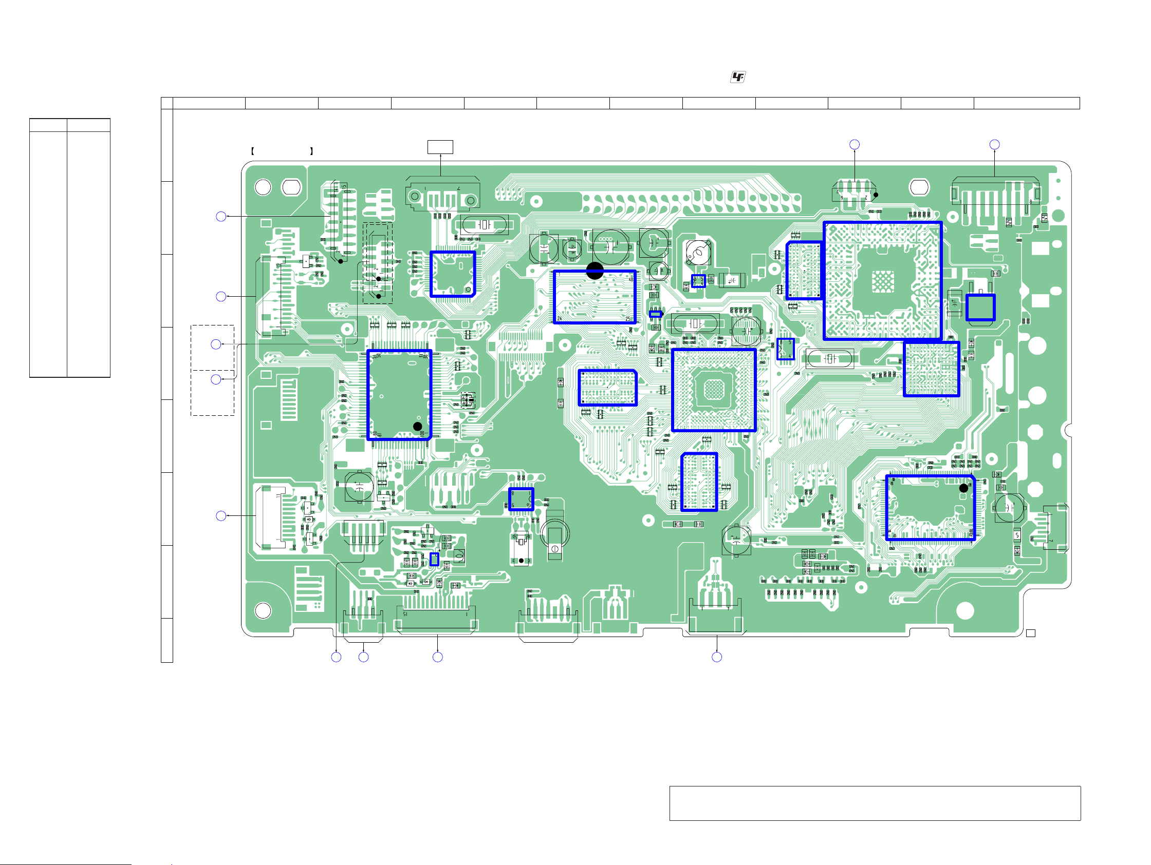
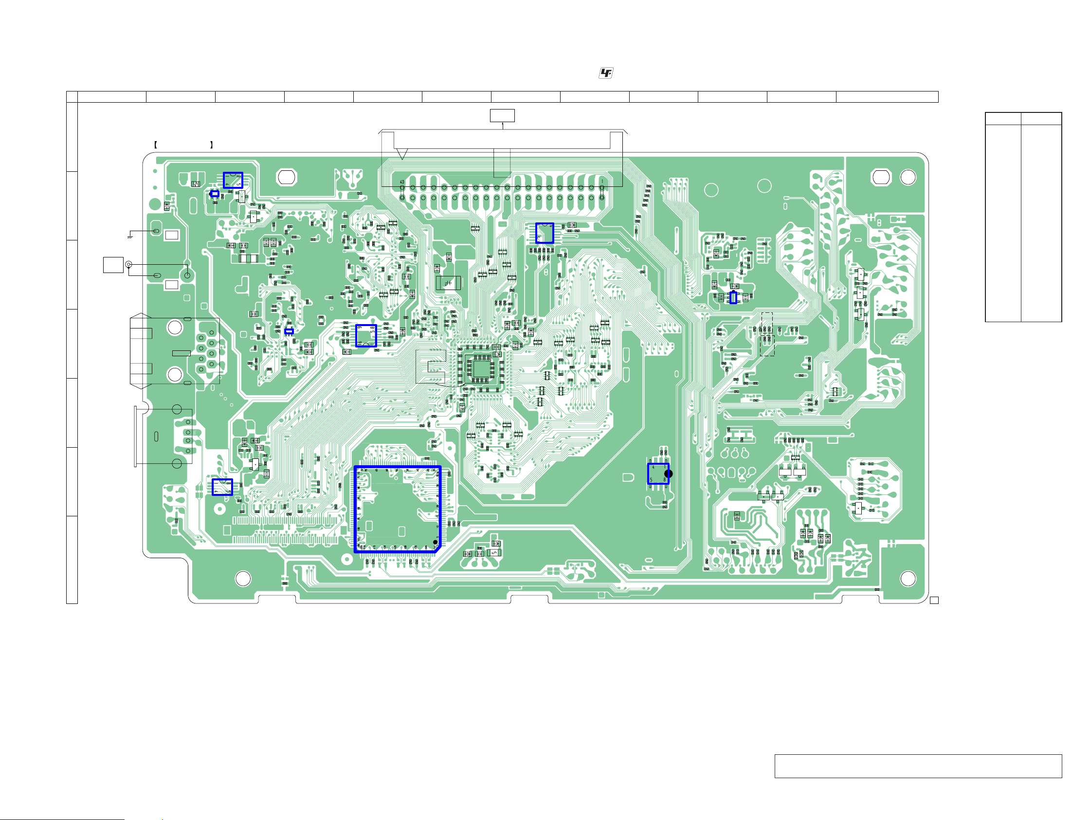
THIS NOTE IS COMMON FOR PRINTED WIRING BOARDS AND SCHEMATIC DIAGRAMS.
(In addition to this, the necessary note is printed in each block.)
• A : B+ Line.
• Voltages and waveforms are dc with respect to ground
under no-signal conditions.
no mark : TUNER
[ ] : CD PLAY
*
: Impossible to measure
• Voltages are taken with VOM (Input impedance 10 MΩ).
• Circled numbers refer to waveforms.
• Signal path.
F : AUDIO
d : TUNER
: DAB
J : CD PLAY
a : USB
f : HDD
G : LAN
k : DMPORT
i : AUDIO IN
L : VIDEO
For Printed Wiring Boards.
Note:
• X : Parts extracted from the component side.
• Y : parts extracted from the conductor side.
• f : internal component.
• : Pattern from the side which enables seeing.
(The other layers' patterns are not indicated.)
• Indication of transistor.
Caution:
Parts face side:
(SIDE A)
Pattern face side:
(SIDE B)
Parts on the parts face side seen from
the pattern face are indicated.
Parts on the pattern face side seen from
the parts face are indicated.
• Lead layouts
surface
CSP (Chip Size Package) Lead layout of conventional IC
Note: The components identifi ed by mark 0 or dotted
line with mark 0 are critical for safety.
Replace only with part number specifi ed.
Caution:
Parts face side:
(Conductor Side)
Pattern face side:
(Component Side)
Parts on the parts face side seen from
the pattern face are indicated.
Parts on the pattern face side seen from
the parts face are indicated.
• MOTHER board is multi-layer printed board.
However, the patterns of intermediate-layers have not
been included in diagrams.
C
Q
B
E
These are omitted.
PANEL (TOP) board
PANEL (FRONT) board
LCD board
MAIN board
HP/AUDIO board
TUNER (FM/AM)
SP/DM board
USB board
MODULE (DAB tuner)
(UK model)
DAB PS board
(UK model)
MOTHER board
NAS-S55HDE/SS-S55HDE
NAS-S55HDE/SS-S55HDE
2828
IC851
C21
C22
C1403
C1404
C1412
C1413
R11
C1418
C1419
R860
IC1902
IC1001
C1416
C9902
R1011
FB2101
C2101
R1091
R1020
R1034
R1036
C3023
C3024
C3029
C3030
C3031
C4024
IC9201
IC9101
C4033
IC1402
C857
X502
C4501
C4502
C9124
C9116
C1902
C4006
C9100
C9125
R4033
C4025
C9117
C9122
C9900
CN1
R1010
D501
FB1402
FB2001
FB4001
R859
R858
FB4501
FB4502
FB9101
R857
IC1002
C1903
C1904
IC3001
R856
IC9301
R855
R854
IC2201
R901
R902
R904
R905
R906
R907
R908
R909
R911
R915
R916
R917
R918
R919
R1107
R1302
R1404
R1405
R1410
R853
R1024
R1602
R852
X5001
C2001
R851
Q851
R1033
R3013
L803
R3017
R3020
R3026
R3027
R3028
R3029
R3030
R3031
R3032
R3033
FB803
C9112
C4002
C4004
C4005
C4015 C4008C4012 C4010C4014 C4011
FB4003
C4013
C4016
C4026
R5014
R5013
C4027
C4028
C4021
R9205
R9206
R9207
R9208
R9209
R4034
R4013
RB9302
L1902
R4008
R4005
R4012
C1092
C1091
R1092
R601
R1022
R1023
R1014
R1021
RB9303
RB9301
RB9304
R4007
R4009
CN4002
CN511
CN8
CN50
5
CN504
CN501
CN201
FB504
D851
C7
C4503
IC2001
IC2101
R4028
C5005
D852
C5004
R4011
R4014
R4004
R4027
X1701
R1501
CN851
C4001
R4006
R4032
R4031
R4010
R1502
R1503
C856
FB4002
RB1501
RB1503
FB806
RB1505
RB1507
RB1508
RB1509
FB501
C855
C854
X1001
RB2204
RB2203
RB2106
RB2105
RB2102
RB2101
RB2006
RB2005
C522
C510
C852
FB1404
C851
C1421
C1420
CN503
C9
IC9901
C508
C509
C512
C523
CN9201
C520
C525
C527
FB131
R501
R502
R503
C4019
FB130
C5019
C5020
C5021
C5022
IC501
Q501
F4501
R597
R590
IC502
R535
R538
R537
R534
R545
R595
R596
R591
R592
R603
R593
R617
R562
R542
R614
R13
R583
R612
R604
R608
R605
FB119
R613
R539
X501
R615
R626
CN510
R2205
R5027
R5029
R5030
R5031
Q510
Q508
C507
Q504
RB501RB502
RB503
RB505
RB507
RB508
RB510
R564
CN852
IC5001
R861
C860
CN5002
C1999
1-874-918-
21
MOTHER BOARD (COMPONENT SIDE)
1
16
48
49 64
32 17
33
F
USB BOARD
CN4801
B
LCD BOARD
CN2504
D
MAIN BOARD
W301
C
PANEL (TOP)
BOARD
CN850
A
MAIN BOARD
W303
G
MAIN BOARD
CN109
M
PANEL (FRONT)
BOARD
CN852
K
MAIN
BOARD
CN111
J
MAIN
BOARD
CN701
Y
MAIN
BOARD
CN112
Z
MAIN
BOARD
CN113
6
7
E
E
E
14
(AEP)
(AEP)
(UK)
(UK)
13
4
5
13
(NC)
(NC)
17
E
E
1
5
8
4
14
404 403 402 401 400 399 398 397 396 395 394 393 392 391 390 389 388 387 386 385 384 383
382 381 380 379 378 377 376 375 374 373 372 371 370 369 368 367 366 365 364 363 362 361
360 359 358 357 356 355 354 353 352 351 350 349 348 347 346 345 344 343 342 341 340 339
338 337 336 335 334 333 332 331 330 329 328 327 326 325 324 323 322 321 320 319 318 317
316 315 314 313 312 311 310 309 308 307 306 305 304 303 302
269 268 267 266 265 264 263 262
301 300 299 298 297 296 295
289 288 287 286 285
279 278 277 276 275
261 260 259 258 257274 273 272 271 270
251 250 249 248 247 246 245 244
243 242 241 240 239256 255 254 253 252
233 232 231 230 229 228 227 226
225 224 223 222 221238 237 236 235 234
215 214 213 212 211 210 209 208
207 206 205 204 203220 219 218 217 216
197 196 195 194 193 192 191 190
189 188 187 186 185202 201 200 199 198
179 178 177 176 175 174 173 172
171 170 169 168 167184 183 182 181 180
161 160 159 158 157 156 155 154
153 152 151 150 149166 165 164 163 162
143 142 141 140 139 138 137 136
135 134 133 132 131148 147 146 145 144
125 124 123 122 121130 129 128 127 126
115 114 113 112 111120 119 118 117 116
110 109 108 107 106 105 104 103 102 101 100
99 98 97 96 95 94 93 92 91 90 89
77 76 75 74 73 72 71 7085 84 8388 87 86 82 81 80 79 78 69 68 67
55 54 53 52 51 50 49 4863 62 6166 65 64 60 59 58 57 56 47 46 45
33 32 31 30 29 28 27 2641 40 3944 43 42 38 37 36 35 34 25 24 23
11 10 9 8 7 6 5 419 18 1722 21 20 16 15 14 13 12 3 2 1
284 283 282 281 280
294 293 292 291 290
37 36 35 34 303332 31 29 28 27 26 25
38 79 78 76 727574 73 71 70 69
68
77 24
91 95
928990
93 94 96 97 60 15
39 80
113 111 107
110
109 108 106 105112
23
6740 81
114 138 134
137
136 135 133 104139
22
6146 87
120 122 126
123
124 125 127121
47 88
52 56
535051
54 55 57 58 59 1448 49
59
634
7 8 10 11 12 1312
16
6641 82
115 132 103140
21
6542 83
116 131 102141
20
6443 84
117 130 101142
19
6344 85
118 129 100143
18
6299
98
45 86
119 128144
17
Y1Y2W1W2V1
U1
T1
R1
P1
N1
M1
L1K1J1 H1
G1
F1
E1D1C1
B1 A1
Y3 W3 V3
U3
T3
R3
P3
N3
M3
L3K3J3 H3
G3
F3
E3D3C3
B3 A3
Y4 W4 V4
U4
T4
R4
P4
N4
M4
L4K4J4
M9
L9K9J9
H4
G4
F4
E4D4C4
B4 A4
Y5 W5 V5
U5
D5C5B5 A5
Y6 W6 V6
U6
D6C6B6 A6
Y7 W7 V7
U7
D7C7B7 A7
Y8 W8 V8
U8
D8C8B8 A8
Y9 W9 V9
U9
D9C9B9 A9
M10
L10
K10
J10
Y10
W10
V10
U10
D10
C10
B10 A10
M11
L11
K11
J11
Y11
W11
V11
U11
D11
C11
B11 A11
M12
L12
K12
J12
Y12
W12
V12
U12
D12
C12
B12 A12
Y13
W13
V13
U13
D13
C13
B13 A13
Y14
W14
V14
U14
D14
C14
B14 A14
Y15
W15
V15
U15
D15
C15
B15 A15
Y16
W16
V16
U16
D16
C16
B16 A16
M18
L18
K18 J18
H18
G18
F18
E18
Y18
W18
V18
U18
T18
R18
P18
N18
D18
C18
B18 A18
M17
L17
K17 J17
H17
G17
F17
E17
Y17
W17
V17
U17
T17
R17
P17
N17
D17
C17
B17 A17
M19
L19
K19 J19
H19
G19
F19
E19
Y19
W19
V19
U19
T19
R19
P19
N19
D19
C19
B19 A19
M20
L20
K20 J20
H20
G20
F20
E20
Y20
W
20 V20
U20
T20R20 P20
N20
D20
C
20
B20 A20
V2
U2
T2
R2
P2
N2
M2
L2K2J2 H2
G2
F2
E2D2C2
B2 A2
HARD DISK
DRIVE (1/2)
A
B
C
D
E
F
G
H
1234567891011 12
(Page 40)
5-5. PRINTED WIRING BOARD - MOTHER Board (Component Side) -
• : Uses unleaded solder.
• See page 27 for Circuit Boards Location.
Note: CN5002, IC501, IC1001, IC1002, IC2001, IC2101, IC5001, IC9101, IC9201 and IC9301 on the MOTHER
board cannot exchange with single. When CN5002, IC501, IC1001, IC1002, IC2001, IC2101, IC5001,
IC9101, IC9201 and IC9301 on the MOTHER board are damaged, exchange the entire mounted board.
Ref. No. Location
• Semiconductor
Location
D501 F-2
D851 G-4
D852 G-4
IC501 D-4
IC502 F-5
IC851 G-4
IC1001 D-8
IC1002 D-9
IC1402 C-7
IC1902 C-8
IC2001 D-6
IC2101 F-8
IC2201 C-6
IC3001 F-11
IC5001 C-4
IC9101 D-11
IC9201 C-10
IC9301 C-9
IC9901 C-12
Q501 F-3
Q504 C-2
Q508 F-2
Q510 F-2
Q851 F-4
(Page 40)
(Page 40)
(Page 40)
(Page 48)
(Page 41)
(Page 50)
(Page 49)
(Page 52)
(Page 41)
(Page 40)
NAS-S55HDE/SS-S55HDE
NAS-S55HDE/SS-S55HDE
2929
5-6. PRINTED WIRING BOARD - MOTHER Board (Conductor Side) -
• : Uses unleaded solder.
• See page 27 for Circuit Boards Location.
Note: IC9401 on the MOTHER board cannot exchange with single. When IC9401
on the MOTHER board is damaged, exchange the entire mounted board.
Ref. No. Location
• Semiconductor
Location
D502 F-11
D503 F-11
IC503 F-9
IC1401 B-7
IC1701 D-5
IC3002 F-3
IC4001 F-5
IC5003 C-10
IC9102 D-4
IC9401 B-3
IC9402 B-2
Q502 D-12
Q503 C-12
Q505 F-12
Q509 C-12
Q512 F-10
Q513 F-11
Q3001 F-3
Q9401 B-3
Q9402 B-3
J1
J2
J3
R618
IC5003
C1000
C1002
C1003
C1004
C1005
C1006
C1101
C1102
C1103
C1104
C1105
C1106
C1107
C1108
C1109
C1110
C1111
C1112
C1113
C1114
C1115
C1116
C1201
C1202
C1203
C1204
C1205
C1206
C1207
C1208
C1209
C1210
C1211
C1212
C1213
C1214
C1215
C1216
C1401
C1402
C1405
C1406
C1407
C1408
C1409
C1410
C1411
C1414
C1415
C1701
C1702
C1703
R1017
IC9102
R1019
R1027
R1025
R1026
R1001
R1028
R1029
R1030
R1031
R1037
R1038
C3007
C3008
C3009
C3010C3011
C3012
C3016
C3017
C3018
C3019
C3020
C3022
C3025
C3026
C3027
C3028
C3032
IC1701
IC4001
R4017
C9248
C9311
C9318
C9314
C9316
C9304
C9214
C9301
C9201
C9212
C4201
C4202
C9313
IC9401
C9317
C9302
C9400
R9203
R9201
R9403
C9264
C9206
R9400
R9404
R9401
C9202
C9208
C9220
C9219
C9258
C9230
C9217
C9312
C9216
C9303
C9213
C9251
C9209
C9261
C9401
C9262
C9247
C9205
C9245
C9232
C9203
C9270
RB9305
C9241
C9225
C9204
C9231
C9190
C9120
C9223
C9207
C9221
C9260
C9222
C9218
C9259
F4502
C9257
C9254
C9256
C9215
C9211
C9255
C9210
C9252
C9253
C9263
C9250
C9224
C9246
C9244
C9243
C9242
C9200
C4022
C9110
C9249
R9202
C9102
C9115
C9119
C9107
C9240
Q513
FB1010
R10
FB1001
FB1003
FB1004
FB1401
FB1403
FB1701
FB1901
FB3001
FB3004
C9109
FB4201
FB4202
C5001
FB9201
FB9301
IC1401
C2201
C2202
IC3002
C9111
C9315
C9300
R2201
Q3001
Q9402
R4018
R903
R910
R912
R913
R914
R1000
R1002
R1003
R1004
R1006
R1007
R1008
R1009
R1101
R1102
R1104
R1105
R1106
R1301
R1303
R1304
R1305
R1306
R1401
R1402
R1403
R1406
R1407
R1408
R1409
R1411
R1601
R1603
R1604
R1701
R1702
R1703
R1704
C9113
R91
C5016
R598
R586
C9108
R90
L802
C9105
C9104
C9106
C9101
C9103
C9118
Q9401
C2002
C2003
C1707
L801
C4023
C4003
C2004
C2005
FB854
R9210
R4015
C2006
FB853
RB1301
RB1302
RB1303
RB1304
RB1305
RB1306
R1112
C2007
C2008
C2009
C2010
R1015
FB852
C2011
C2012
C2013
C2102
C2103
C2104
C2105
R1016
RB9308
RB9306
RB9307
FB851
R616
FB5003
FB5002
FB5001
C805
C2106
C2107
C2108
C3
C2109
FB9100
C2110
FB1702
C505
C2111
C2112
C2113
C5013
R4023
R4024
R1710
C1001
R1709
IC9402
R4016
C9114
R9204
RB1502
C506
FB126
FB132
RB1504
RB1506
RB2001
RB2002
R1111
R1707
RB2003
RB2202
RB2201
RB2108
RB2107
RB2104
RB2103
RB2008
RB2007
RB2004
C853
R1043
R1042
R1041
R1040
FB133
FB125
FB128
FB121
C1706
C1705
C1704
C1118
C1117
R87
FB9292
FB129
R2202
R1711
R1044
C511
C513
C515
C516
C519
C521
C526
C517
FB127
FB134
C5014
C5002
R504
R505
C5006
C5007
C5008
C5009
C5010
C5011
FB124
C5015
FB123
FB122
R506
R507
R512
R529
R518
R523
R524
R525
R527
FB120
D503D502
R546
R552
R619
R547
R576
IC503
R563
R585
R642
R572
R571
R579
R508
R584
R587
R600
R588
R582
R553
R511
R624
R625
R632
R633
R636
R637
R639
R575
Q509
R611
Q503
Q502
FB136
R2203
R5011
R5010
R5015
R5016
Q512
R5019
R5020
R5036
R5041
R5042
R622
Q505
R606
RB506
RB509
R530
FB135
FL9202
C859
C858
C801
C802
CN7
MOTHER BOARD (CONDUCTOR SIDE)
1
3
4
5
1
9
16
8
1-874-918-
21
CD-ROM
DRIVE (1/2)
1
34
2
E
E
E
1
4
1
7
2
8
(USB)
NETWORK
1
3
4
5
E
E
E
KEKKK
AA
EE
MONITOR
OUT
(NTSC)
(CHASSIS)
A
B
C
D
E
F
G
1234567891011 12
(AEP)
(UK)
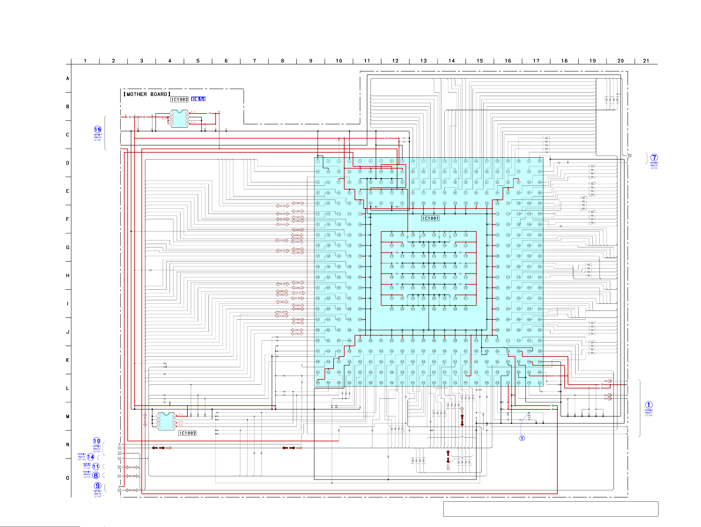
NAS-S55HDE/SS-S55HDE
NAS-S55HDE/SS-S55HDE
3030
RB1508
RB1502
RB1503
RB1504
R1502
RB1505
RB1506
RB1507
C1402 C1401C1403C1404R1402R1401
X1001
C1091 C1092
R1092
C1004
C1005
C1003
C1002
R1091
R1404
R1405
R1403
C1405
TP1501
R1501
RB1501
R1503
C1109
C1110
C1111
C1112
C1116
R1001
R1000
C1000
RB1303
RB1302
R1306
R1305
RB1304
RB1305
RB1306
R1002
R1009
TP1001
TP1000
R1016
R1015
C1115
C1215 C1216
C1212
C1211
C1210
C1209
C1204
C1104
R1043
C1118
R1040R1041
C1102
C1201
C1205
C1206
C1207
C1208
C1214C1213
C1113 C1114
R1303
R1302
RB1301
R1011
R1301
R1304
R1102
R1105
R1104
R1106
C1108
C1107
C1106
C1105
C1101
R1111
R1101
R1006
R1007
R1031
R1030
R1004
R1020
R1112
R1037
R1107
L1902
4.7μH
TP1903
TP1904
C1902
R1038
R1023
R1024
R1022
R1021
R1025R1026R1044
TP1902
C1001
C1904
TP1901TP1002
R1010
R1034
R1019
R1017
R1027
R1028
R1029
R1036
IC1002
C1006
FB1001
FB1901
FB1401
FB1402
FB1004
FB1003
C1103
C1202 C1203
TP1905
RB1509
R1014
R1003
C1117R1042
IC1902
IC1001
TP1003
C1903
22
47
47
47
47
47
47
47
0.1 10100.1180180
25MHz
10p 6p
330
10
1
1
10
1M
3.3k
470
180
0.1
10
47
47
1
1
1
1
1
10k
1k
0.1
33
22
5.6k
82
33
33
33
1k
10k
10k
0
1
11
1
1
1
1
1
1
0
0.1
5.6k5.6k
1
1
1
1
1
1
11
11
82
33
33
1k
82
1k
10k
10k
10k
10k
1
1
1
1
1
10k
10k
2.2k
R1033
10k
R1008
0
2.2k
0
0
1k
1k
100k
100k
10k
10
100k
100k
100k
100k
100k
100k100k100k
100
6.3V 10
10k
100k
0
1k
0
0
1k
10k
CAT24C04YI-GT3
1
1
11
47
0
10k
100
R1232D121B-TR-F
R5S70901Y300BGV
100
6.3V
C1999
100
16V
+3.3VSB
GND
SDRAM_CLK
+3.3V
VBUS
XSATARESET
DAC
DACVBS
VIDEO-GND
VCCA
DPSCLK
PCICLK
DAY
IDE_BUS
PCI_BUS
PCI_BUS
PCI_BUS
PCI_BUS
CONTROL BUS
SDRAM BUS
TXD0
TXD1
RXD0
RXD1
XIDERST
INTRQ
IORDY
XCS0
XCS1
DMARQ
DA0
DA1
DA2
DD0
DD1
DD2
DD3
DD4
DD5
DD6
DD7
DD8
DD9
DD10
DD11
XRESET
CKE
XRAS
XCAS
XWE
A4
A5
A6
A7
A8
A9
A10
A11
A12
A13
A14
A15
A16
A17
A18
A19
A20
A21
A22
XINTB
XINTD
XINTC
DQMLL
DQMUL
DQMLU
DQMUU
XRD
XCS0
XRESET
BOOTMODE0
STATUS
BOOTMODE1
RXD2
TXD2
IRQ1
AD30
AD25
AD27
AD28
AD26
AD23
XCBE3
AD24
AD19
AD21
AD22
AD20
XCBE2
AD17
AD18
AD16
XDEVSEL
XIRDY
XFRAME
XTRDY
XPERR
XSTOP
PAR
XCBE1
XSERR
AD15
AD13
AD12
AD14
AD11
AD9
AD8
AD10
XCBE0
AD6
AD5
AD7
AD4
AD3
AD2
AD1
AD0
XGNT1
XPCIRST
XINTA
XREQ1
XREQ0
XGNT0
XREQ2
D61
D62
D63
D38
D46
D47
D32
D33
D34
D35
D36
D37
D43
A0
A1
A2
A3
XCS1
D42
D44
D45
D40
D41
XGNT2
AD29
AD31
D52
D53
D54
D55
D39
DQM64UU
DQM64UL
DQM64LL
DQM64LU
14
13
36
35
35
36
13
14
D50
D51
D56
D57
D48
D49
D58
D59
D60
D22
D23
D24
D25
D21
D26
D27
D20
D28
D29
D19
D18
D31
D30
D16
D17
D7
D8
D9
D10
D11
D5
D4
D12
D13
D3
D2
D14
D15
D6
D1
D0
DD12
DD13
DD14
DD15
372
372
393
371
392
XDIOR
XDIOW
XDMACK
349
348
327
348
327
349
392
371
393
A0
A1
A2
GND
VCC
WP
SCL
SDA
XC2
VDDPLL2
VCCA1 VSSQ
XRD IDERST VSSPLL2 VSSCA VCCA VSSCA1
DACCBU1VSSCAVSSPLL1XTALDPSCLK
RDY EXTAL VDDPLL1 DACVBS DAY REXT1
XBS
NMI
RESETNVDIR
IDSEL
LOCK
PA0
PA7PA6
PA5
PA4 FCE MODE8
MODE7PA2IRQ0
MODE0MODE3
MODE4 MODE1MODE6
IRQOUT
SCL SDA MODE5 MODE2
PA1
PA3
XOUT
XIN
DP1 DM1
DP0
DM0
VSSQU0
VBUS1 VDDQU1 VDDQAU0 VBSO
PCICLKOUT VSSU1 VSSAU1 VSSQU1 VSSU0
VDDU0VDDAU1VDDAU1VDDU1
VDDQU0
VSSAU0
VDDAU0
REFRIN0VSSQAU0REFRIN1VSSQAU1
GND
VIN
VDD
CE
AGND
VOUT
MODE
LX
+1.2V REGULATOR
(1/10)
EEPRAM
CSP
(Chip Size Package)
CPU
5-7. SCHEMATIC DIAGRAM - MOTHER Board (1/10) -
• See page 53 for waveforms. • See page 55 for IC Block Diagrams. • See page 63 for IC Pin Function Description.
(Page 35)
(Page
31)
Note: IC1001 and IC1002 on the MOTHER board cannot exchange with single. When IC1001
and IC1002 on the MOTHER board are damaged, exchange the entire mounted board.
(Page 35)
(Page 34)
(Page
36)
(Page
33)
(Page 39)
(Page
32)
 Loading...