

Page 1
SERVICE MANUAL
US Model
Canadian Model
Singapore Model
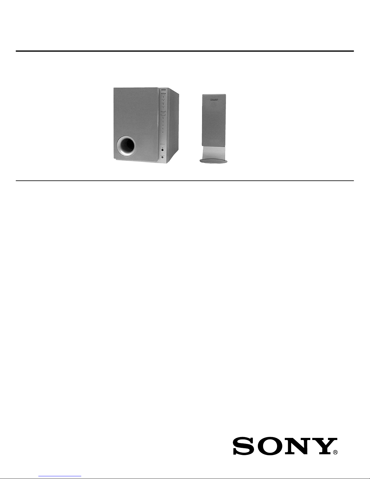
ACTIVE SPEAKER SYSTEM
SA-F21
SPECIFICATIONS
SA-WMS21 SS-MS21
AUDIO POWER SPECIFICATIONS: (US model only)
POWER OUTPUT AND TOTAL HARMONIC
DISTORTION:
With 4 ohm loads, both channels driven, from 40–
20000 Hz; rated 12 watts per channel minimum
RMS power, with no more than 1 % total
harmonic distortion from 200 milli watts to rated
output.
Satellite speakers (SS-MS21)
Speaker system Full range, antimagnetic
speaker
Speaker unit 8 cm (3
1
/
4
in.), cone type
Enclosure type Bass reflex
Rated impedance 4 ohms
Power handling capacity
Maximum input power
30 W
Sensitivity level 79 dB (1 W, 1 m)
Frequency range
150 to 20,000 Hz
Dimensions (approx.)
90 × 200 × 64 mm (3
5
/
8
×
7
7
/
8
× 2
5
/8 in.) (w/h/d)
including projecting parts
Mass (approx.) 630 g (1 lb. 6 oz.)/piece
Subwoofer system (SA-WMS21)
Speaker system Active subwoofer,
antimagnetic
Speaker unit 13 cm (5
1
/
8
in.), cone type
woofer, dual voice coil
Enclosure type Bass reflex
Reproduction frequency range
40 to 150 Hz
Power Output
Satellite speaker 15 W × 2
Subwoofer 15 W + 15 W
Input jack
INPUT Pin jack
Output jack
SPEAKER IMP 4Ω Speaker jack
HEADPHONES Stereo mini jack
General
Power requirements
120 V AC, 60 Hz (US, Canadian models)
Power consumption
60 W (Singapore model)
55 W (US, Canadian models)
220 – 230 V AC, 50/60 Hz (Singapore model)
Dimensions (approx.)
190 × 266 × 375 mm (7
1
/
2
×
10
1
/
2
× 14
7
/8 in.) (w/h/d)
including projecting parts
Mass (approx.) 7.0 kg (15 lb. 7 oz.)
Design and specifications are subject to change
without notice.
Page 2
– 2 –
WARNING!!
WHEN SERVICING, DO NO T APPR O A CH THE LASER
EXIT WITH THE EYE TOO CLOSELY. IN CASE IT IS
NECESSARY TO CONFIRM LASER BEAM EMISSION,
BE SURE TO OBSERVE FROM A DISTANCE OF
MORE THAN 25 cm FROM THE SURFACE OF THE
OBJECTIVE LENS ON THE OPTICAL PICK-UP BLOCK.
ATTENTION AU COMPOSANT AYANT RAPPORT
À LA SÉCURITÉ!
LES COMPOSANTS IDENTIFIÉS P AR UNE MARQUE 0
SUR LES DIAGRAMMES SCHÉMA TIQUES ET LA LISTE
DES PIÈCES SONT CRITIQUES POUR LA SÉCURITÉ
DE FONCTIONNEMENT. NE REMPLACER CES COMPOSANTS QUE PAR DES PIÈCES SONY DONT LES
NUMÉROS SONT DONNÉS DANS CE MANUEL OU
DANS LES SUPPLÉMENTS PUBLIÉS PAR SONY.
SAFETY-RELATED COMPONENT WARNING!!
COMPONENTS IDENTIFIED BY MARK 0 OR DOTTED
LINE WITH MARK 0 ON THE SCHEMATIC DIA GRAMS
AND IN THE PARTS LIST ARE CRITICAL TO SAFE
OPERATION. REPLACE THESE COMPONENTS WITH
SONY PARTS WHOSE PART NUMBERS APPEAR AS
SHOWN IN THIS MANUAL OR IN SUPPLEMENTS PUBLISHED BY SONY.
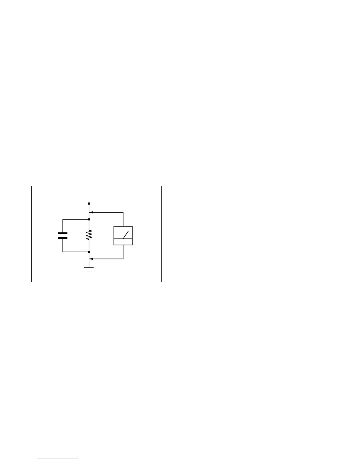
Fig. A. Using an AC voltmeter to check AC leakage.
1.5 k
Ω
0.15 µF
AC
voltmeter
(0.75 V)
To Exposed Metal
Parts on Set
Earth Ground
LEAKAGE TEST
The AC leakage from any exposed metal part to earth ground
and from all exposed metal parts to any exposed metal part having
a return to chassis, must not exceed 0.5 mA (500 microamperes).
Leakage current can be measured by any one of three methods.
1. A commercial leakage tester , such as the Simpson 229 or RCA
WT -540A. Follow the manufacturers' instructions to use these
instruments.
2. A battery-operated AC milliammeter. The Data Precision 245
digital multimeter is suitable for this job.
3. Measuring the voltage drop across a resistor by means of a
VOM or battery-operated AC voltmeter. The “limit” indica-
tion is 0.75V, so analog meters must have an accurate low-
voltage scale. The Simpson 250 and Sanwa SH-63T rd are ex-
amples of a passive VOM that is suitable. Nearly all battery
operated digital multimeters that have a 2V A C range are suit-
able. (See Fig. A)
1. Check the area of your repair for unsoldered or poorly-soldered connections. Check the entire board surface for solder
splashes and bridges.
2. Check the interboard wiring to ensure that no wires are
“pinched” or contact high-wattage resistors.
3. Look for unauthorized replacement parts, particularly transistors, that were installed during a previous repair. Point them
out to the customer and recommend their replacement.
4. Look for parts which, though functioning, show obvious signs
of deterioration. Point them out to the customer and recommend their replacement.
5. Check the line cord for cracks and abrasion. Recommend the
replacement of any such line cord to the customer.
6. Check the B+ voltage to see it is at the values specified.
7. Check the antenna terminals, metal trim, “metallized” knobs,
screws, and all other exposed metal parts for AC leakage.
Check leakage as described below.
SAFETY CHECK-OUT
After correcting the original service problem, perform the following
safety checks before releasing the set to the customer:
Page 3

– 3 –
1. GENERAL............................................................ 1-1
2. BLOCK DIAGRAMS
2-1. Overall Block Diagram .................................................. 2-1
2-2. Audio/control Block Diagram ........................................ 2-3
2-3. Power Block Diagram .................................................... 2-5
3. PRINTED WIRING BOARDS AND
SCHEMATIC DIAGRAMS
3-1. Circuit Boards Location ................................................. 3-2
3-2. Frame Schematic Diagram ........................................... 3-3
3-3. Printed Wiring Boards and Schematic Diagrams ......... 3-5
Main, Jack, Sub Transformer
Printed Wiring Boards ................................................... 3-5
Main, Jack, Sub Transformer
Schematic Diagram ....................................................... 3-7
Control Printed Wiring Board ........................................ 3-9
Control Schematic Diagram .......................................... 3-11
Power, Speaker Terminal Printed Wiring Boards .......... 3-14
Power, Speaker Terminal Schematic Diagram.............. 3-15
4. REPAIR PARTS LIST
4-1. Exploded Views ............................................................. 4-1
4-1-1. SA-WMS21............................................................... 4-1
4-1-2. SS-MS21 .................................................................. 4-2
4-2. Electrical Parts List........................................................ 4-3
TABLE OF CONTENTS
Section Title Page
Page 4
SA-F21
1-1 1-2 E
SECTION 1
GENERAL
This section is extracted from instruction manual (3-071-506-11).
English
Warning
To prevent fire or shock hazard, do not expose
the unit to rain or moisture.
This symbol is intended to alert the user
to the presence of uninsulated
“dangerous voltage” within the
product’s enclosure that may be of
sufficient magnitude to constitute a risk
of electric shock to persons.
This symbol is intended to alert the user
to the presence of important operating
and maintenance (servicing) instructions
in the literature accompanying the
appliance.
For customers in the U.S.A.
Owner’s Record
The model and serial numbers are located at the rear of
the unit. Record the serial number in the space provided
below. Refer to them whenever you call upon your Sony
dealer regarding this product.
Model No. SA-F21
Serial No.______________
NOTE:
This equipment has been tested and found to comply
with the limits for a Class B digital device, pursuant to
Part 15 of the FCC Rules. These limits are designed to
provide reasonable protection against harmful
interference in a residential installation. This equipment
generates, uses, and can radiate radio frequency energy
and, if not installed and used in accordance with the
instructions, may cause harmful interference to radio
communications. However, there is no guarantee that
interference will not occur in a particular installation. If
this equipment does cause harmful interference to radio
or television reception, which can be determined by
turning the equipment off and on, the user is
encouraged to try to correct the interference by one or
more of the following measures:
– Reorient or relocate the receiving antenna.
– Increase the separation between the equipment and
receiver.
– Connect the equipment into an outlet on a circuit
different from that to which the receiver is connected.
– Consult the dealer or an experienced radio/TV
technician for help.
CAUTION
You are cautioned that any changes or modifications not
expressly approved in this manual could void your
authority to operate this equipment.
For customers in Canada
CAUTION
TO PREVENT ELECTRIC SHOCK, DO NOT USE THIS
POLARIZED AC PLUG WITH AN EXTENSION CORD,
RECEPTACLE OR OTHER OUTLET UNLESS THE
BLADES CAN BE FULLY INSERTED TO PREVENT
BLADE EXPOSURE.
Precautions
On safety
Should any solid object or liquid fall into the cabinet,
unplug the speaker system and have it checked by
qualified personnel before operating it any further.
On power sources
•AC power cord must be changed only at the qualified
service shop.
•Before operating the speakers, check that the operating
voltage is identical with your local power supply. The
operating voltage is indicated on the nameplate on the
rear of the speakers.
•The unit is not disconnected from the AC power
source as long as it is connected to the wall outlet, even
if the unit itself has been turned off.
•If you are not going to use the speakers for a long time,
be sure to disconnect the speakers from the wall outlet.
To disconnect the AC power cord, grasp the plug itself;
never pull the cord.
On placement
•Do not install the appliance in a confined space, such
as a bookcase or built-in cabinet.
•Do not place the speakers near heat sources, or in a
place subject to direct sunlight, excessive dust or
mechanical shock.
•Good ventilation is essential to prevent internal heat
buildup. Place the speakers in a location with adequate
air circulation, and in a way that does not block the
rear ventilation holes.
On operation
•When turning on or off the subwoofer or other
equipment, lower the volume of the subwoofer to
minimum.
•To avoid damaging the subwoofer:
– Be careful in setting the volume control of the
subwoofer to avoid an excessive input power.
– Do not open the enclosure or remold speaker units
and networks.
– The grill net is not removable. Do not remove it.
On the speaker system
Although this speaker system is magnetically shielded,
there may be cases where the picture on some TV sets
becomes magnetically distorted. In such a case, turn off
the power of the TV set once, and after 15 to 30 minutes
turn it on again.
If there seems to be no improvement, locate the
speaker system further away from the TV set. Also, be
sure not to place objects in which magnets are attached
or used near the speaker system, such as audio racks, TV
stands, and toys. These may cause magnetic distortion to
the picture due to their interaction with the system.
On cleaning
Clean the cabinet, panel and controls with a soft cloth
slightly moistened with a mild detergent solution. Do
not use any type of abrasive pad, scouring powder or
solvent such as alcohol or benzine.
If you have any question or problem concerning your
speaker system, please consult your nearest Sony dealer.
Setting Up
Step 1: Unpacking
Check that you have the following items:
•Audio cord (with red and white plugs) (1)
•Speaker cords (2.5 m) (2)
•Speaker stands (2)
•Stand screws (8)
•Washers for stand screws (8)
Step 2: Connecting Speakers
Before you start, turn off the power and
disconnect the power cord of each
component.
Refer to the instructions supplied with the
components to be connected.
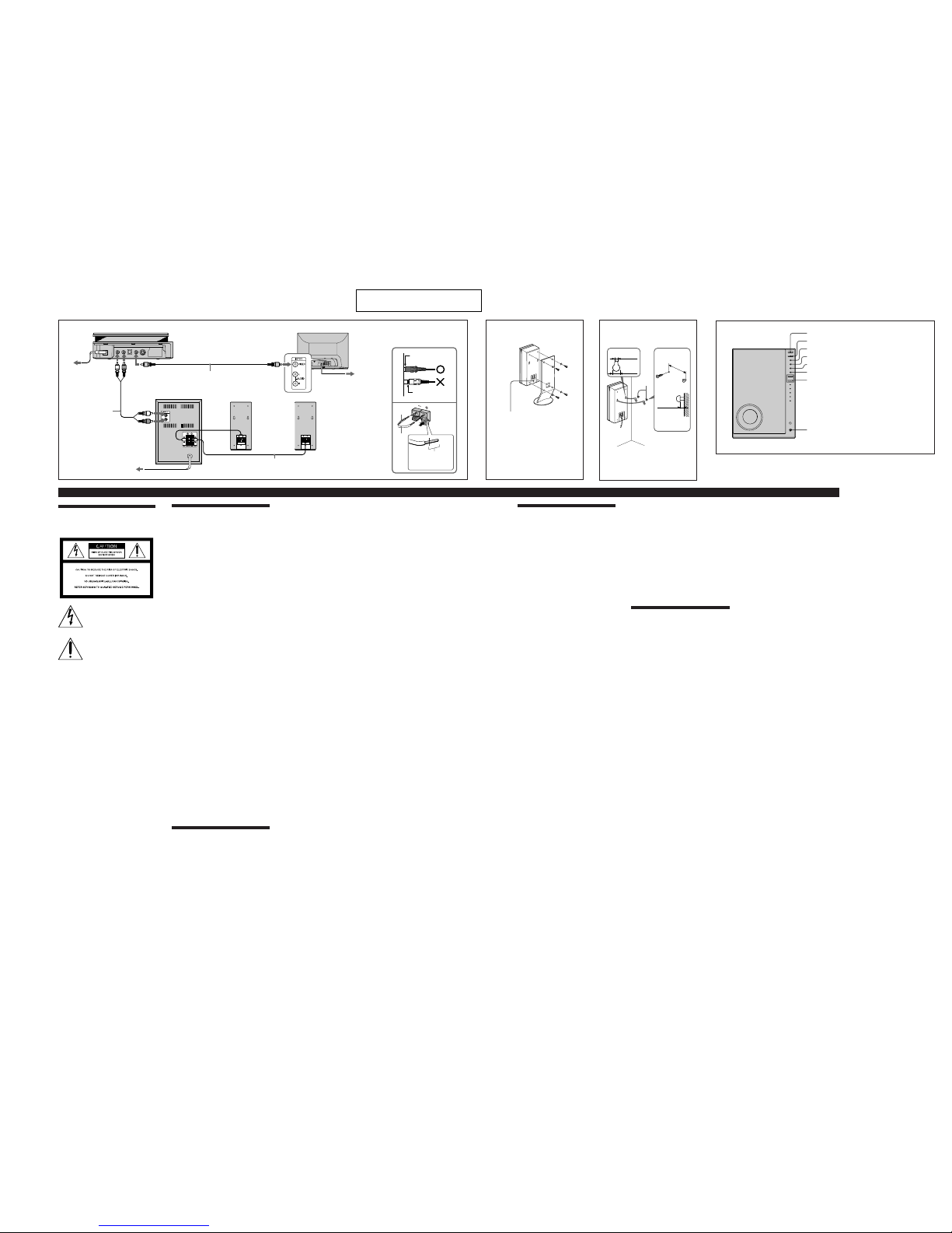
Connecting to the DVP-F21 (fig. A)
1 Connect the player to the TV.
Use a video cord (not supplied). First remove the
jack cover from the player, and then connect the
VIDEO OUT jack of the player with the video
input jack of the TV.
You can use the video/audio cord with red,
white and yellow plugs supplied with DVP-F21
instead of the video cord (not supplied). Connect
the yellow plug only.
If you connect a TV with S VIDEO input jack, use
an S VIDEO cord (not supplied). You will enjoy
high quality images.
2 Connect the player to the subwoofer.
Use the supplied audio cord (with red and white
plugs). Connect the AUDIO OUT L/R jacks of the
player to the INPUT L/R jacks of the subwoofer.
Connect the red plug to the red jack and white
plug to the white jack.
3 Connect the satellite speakers to the
subwoofer.
Use the supplied speaker cords. Connect the cord
with stripe to the # terminal.
Attach the jack cover to the player.
You can install the player in three ways;
horizontal, vertical or on the wall.
See “Step 3: Attaching the Jack Cover” in the
operating instructions supplied with the player.
Notes
•Plug cords securely to prevent unwanted noise. (fig.
A-1)
•Be sure to match the speaker cord to the appropriate
terminal: + to + and – to –. If the cords are reversed,
the sound will be distorted and will lack bass. (fig. A-
2)
Connecting to a component other than
the
DVP-F21
Connect the SA-F21 in the same way as the DVPF21. Connect the audio output L/R (front L/R)
jacks of your player to the INPUT L/R jacks of
the subwoofer in step 2.
Step 3: Installing Speakers
For greater flexibility in the positioning of the
satellite speakers, use the supplied speaker
stands. (fig. B)
Speaker stands WS-FV10A, WS-TV10A, and WSWV10A are also available on option.
You can install the satellite speakers on the wall
using commercially available screws. (fig. C)
You need to determine the appropriate hanging
screws and/or other necessary hardware needed
to securely and safely fasten the speakers to the
wall. Please be sure you have selected fasteners
or screws that will fit in the hanging holes on the
rear of the speaker.
Placement of the screws should be at the same
height and should be 2 3/8 in. (59 mm) apart. The
screws or other fasteners should protrude by
3/16 in. to 7/32 in. (4 to 5 mm). You may also
mark placement of the screws or fasteners by use
of something like a template.
Hang the speakers on the screws and push the
speakers so that they fit against the wall.
BC
A
2 3/8 in.
(59 mm)
Screws
#
3
TV
Satellite speakers
Subwoofer
CD/DVD Player DVP-F21
Notes
•When you install the speakers on the wall, make sure
that the wall is strong enough to hang the speakers.
•When you disconnect or connect the cords, take the
speakers down from the wall.
•For best possible surround sound, place the satellite
speakers on both sides of the TV or monitor equal
distances apart.
Step 4: Connecting the Power
Cord
Connect the power cord of each component to the
wall outlet.
Step 5: Setting Up for the CD/
DVD Player
You may need to make some setups for the
player. Refer to the instructions supplied with the
components to be connected.
If you are using the DVP-F21
When connecting to a wide screen TV, the image
may not fit your TV screen depending on the
disc. If you want to change the aspect ratio, select
“SCREEN SETUP” in the Setup Display and then
adjust the “TV TYPE”setting, see “Settings for the
Display (SCREEN SETUP)” in the operating
instructions supplied with the player.
A-1
A-2
1
2
3
3
/16 – 7/
32
in.
(4 – 5 mm)
Insert up to here.
Video cord (not supplied)
Audio cord (supplied)
Speaker cord (supplied)
to AUDIO OUT L to AUDIO OUT R
to VIDEO OUT
Screw hole to attach the stand
such as WS-FV10A, WS-TV10A,
WS-WV10A (not supplied)
3
/16 in.
(4.5 mm)
3
/8 in.
(9 mm)
Playing the Disc (fig . D)
After connecting and setting up the player, you
can play the disc.
1
Turn on the components.
TV:
Turn on the TV and switch the input selector
on the TV to the player.
Player:
Turn on the player.
2
Press ?/1 (power) on the subwoofer.
The subwoofer is turned on and the power
indicator changes from red (standby) to
green.
3
Press MODE on the subwoofer repeatedly
until the MASTER VOL indicator lights up
in green.
4
Press LEVEL – to turn down the volume to
the minimum.
5
Insert the disc in the player.
6
Press H on the player.
Playback starts. Adjust the volume with
LEVEL +/– on the subwoofer.
Using the headphones
Connect the headphones (not supplied) to the
HEADPHONES jack on the subwoofer.
To adjust the volume, press MODE on the
subwoofer repeatedly until the MASTER VOL
indicator lights up. Then press LEVEL +/–.
z The subwoofer automatically enters
standby mode (Auto Power On/Off function)
If no audio signal is input to the subwoofer for about 3
minutes, the subwoofer automatically enters standby
mode and the ?/1 (power) indicator changes to red.
When an audio signal is input, the subwoofer turns on
automatically and the ?/1 indicator changes to green.
The Auto Power On/Off function works only when no
audio signal is input for about 3 minutes. If you want to
turn off the subwoofer at once, press ?/1 (power) on the
subwoofer.
Adjusting the speakers
To select the volume to be adjusted
1
Press MODE repeatedly to turn on the
desired volume indicator (MASTER VOL for
entire volume or SW VOL for subwoofer
volume).
2
Press LEVEL +/– to adjust the volume.
If you are using the DVP-F21
If you set the TV/DVD switch on the remote to
DVD, you can adjust the entire volume with VOL
+/– on the remote.
zSome of the remote that can control Sony AV
amplifiers (receivers) may be able to control the
volume of this system.
To select a range to be adjusted
1
Press MODE repeatedly to turn on the
desired range indicator (BASS for the low
frequency range or TREBLE for the middle to
high frequency range).
2
Press LEVEL +/– to adjust the volume.
To switch the subwoofer mode to match
the bass output of the sound source
Press LEVEL + and – at the same time on the
subwoofer to switch the subwoofer mode
between MOVIE and MUSIC. The color of the SW
VOL indicator will indicate the current mode.
The default setting is MOVIE.
Mode Color For sound sources such as
MOVIE Green Movies
MUSIC Red Music
To return the volume setting to the default
setting
While pressing LEVEL + and – at the same time,
press ?/1 (power) on the subwoofer.
Troubleshooting Guide
If you experience any of the following difficulties
while using the system, use this troubleshooting
guide to help remedy the problem before
requesting repairs. Should any problem persist,
consult your nearest Sony dealer.
The subwoofer automatically entered
standby mode.
, Auto Power On/Off function worked because
no audio signal had been input for about 3
minutes.
There is no sound from the speakers.
, The system is not connected correctly.
, The system is connected by incorrect
connecting cords.
, The volume is turned down to the minimum.
, The headphones are connected.
Sound is noisy.
, The system is not connected correctly.
, Audio equipment or such is placed close to an
equipment causing noise such as TV.
, The plugs and jacks are dirty.
Sound stops suddenly.
, The system is not connected correctly.
, Short-circuit occurred to the stripped speaker
cord.
D
1
2
3
4
5
6
7
8
Parts and controls
1 ?/1 (power) button/indicator
2 MODE (mode) button
3 MASTER VOL (master volume) indicator
4 SW VOL (subwoofer volume) indicator
5 BASS (bass) indicator
6 TREBLE (treble) indicator
7 LEVEL (level) +/– buttons
8 HEADPHONES (headphones) jack
Page 5
SA-F21
2-1 2-2
SECTION 2
BLOCK DIAGRAMS
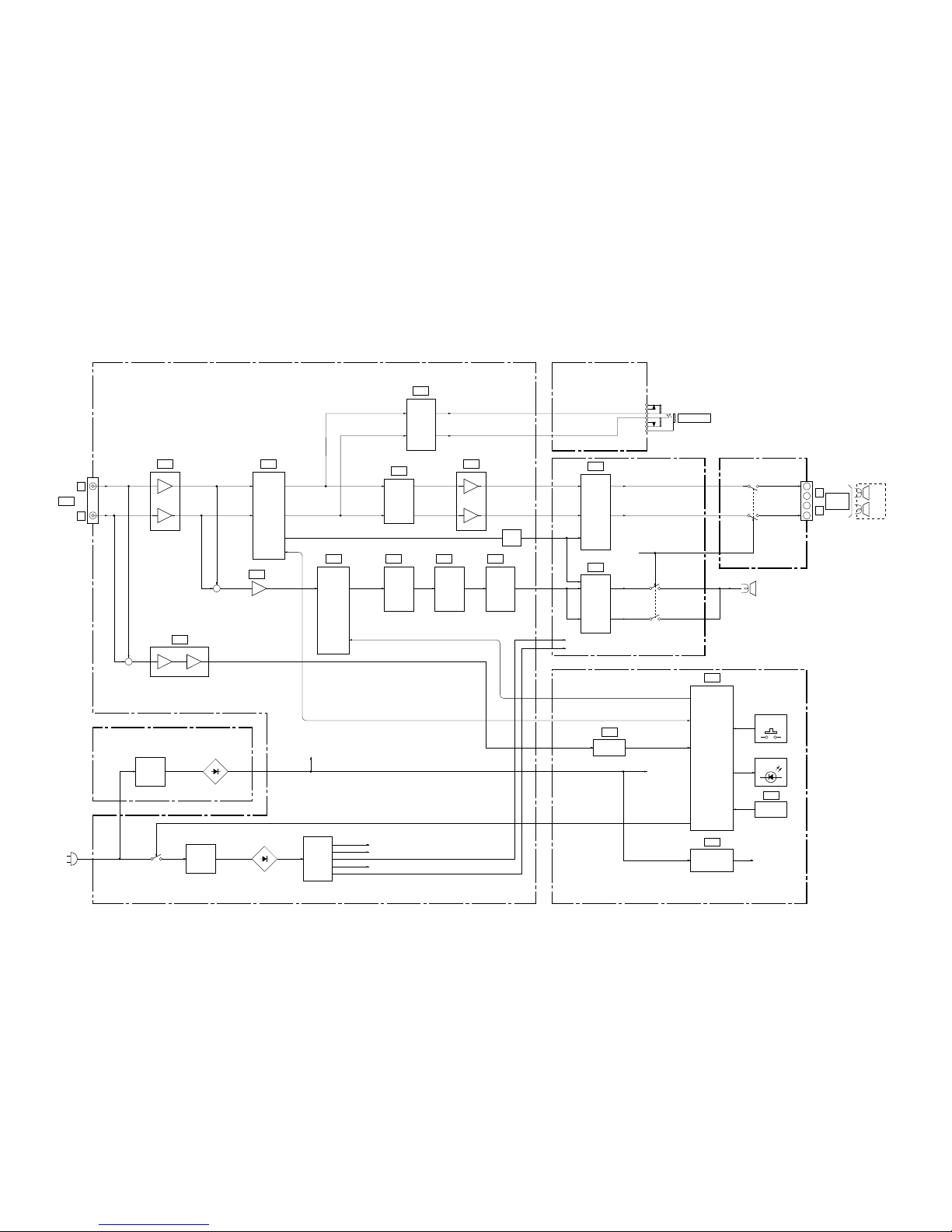
2-1. OVERALL BLOCK DIAGRAM
IC107
IC103
IC109IC101
VOLUME,
TONE
CONTROL
IC104
IC102
HPF
IC301
POWER
AMP
IC601
HEADPHONE
AMP
+
+
IC105 (1/2)
IC105 (2/2)
SOUND
CONTROL
HPF
IC106 (2/2)
LPF
IC106 (1/2)
LIMITER
AMP
MUTE
DRIVE
L
R
INPUT
PJ101
MAIN BOARD
(SEE PAGE 3-7)
JACK BOARD
(SEE PAGE 3-8)
POWER BOARD
(SEE PAGE 3-15)
CONTROL BOARD
(SEE PAGE 3-11)
SPEAKER TERMINAL BOARD
(SEE PAGE 3-16)
SUB TRANSFORMER BOARD
(SEE PAGE 3-7)
AC IN
D810 – 813
D801
T802
T801
+VCC
RY801
HEADPHONES
J601
RY301
+
+
L
R
–
–
SPEAKER
IMP 4Ω
RELAY
CONTROL
IC401
POWER
AMP
RY401
SP101
SUB WOOFER
IC501
IC802
IC502
SYSTEM
CONTROL
REG
+11V
+5V
–11V
+VSS
–VSS
AUTO POWER
DETECT
+5V REG
IC504
MUTE
SW DATA, SW CLK
VOL CLK,
VOL DATA, VOL CE
SW DATA, SW CLK
AUTO SW
STANDBY
VOL CLK, VOL DATA,
VOL CE
+VCC
FUNCTION
SWITCH
S501 – 504
LED
D502 – 511
RESET
+5V
05
L-CH
R-CH
SS-MS21
Page 6

SA-F21
2-3 2-4
2-2. AUDIO/CONTROL BLOCK DIAGRAM
IC106
LIMITER AMP,
LPF
IC102
HPF
3 1
5 7
IC107
LINE AMP
IC105 (1/2)
MIX AMP
IC105 (2/2)
HPF
31 24
2 9
20
IC101
VOLUME,
TONE
CONTROL
IC104
SOUND
CONTROL
3 1
5 7
IC109
AMP
2
6
IC601
HEADPHONE AMP
3 1
5 7
19
18
14
Q601
MUTE
Q602
MUTE
3
4
2
5
1
3
4
2
5
1
HEADPHONES
J601
JACK BOARD
(SEE PAGE 3-8)
POWER BOARD
(SEE PAGE 3-15)
CONTROL BOARD
(SEE PAGE 3-11)
MAIN BOARD
(SEE PAGE 3-7)
SPEAKER TERMINAL BOARD
(SEE PAGE 3-16)
2 1
6 7
IC103
MIX AMP
+
21
19
20
4 5 7 2 1
5 7
Q603
MUTE
Q604
MUTE
B+
+
Q605
MUTE
DRIVE
3
4
5
1
3
4
5
1
Q101, 102
MUTE
DRIVE
Q806
POWER ON
MUTING
D809
1
2
1
2
6
8
4
3
1
INL
RIN
M/S
OUTL
OUTR
IC301
POWER AMP
6
8
4
3
1
IN1
RI2
M/S
OUT1
OUT2
IC401
POWER AMP
IC502
AUTO POWER DETECT
IC501
SYSTEM CONTROL
IC504
RESET SIGNAL
GENERATOR
IC503
REMOTE COMMANDER
RECEIVER
2
3
4
5
1
2
3
4
5
1
+
+
–
–
POWER
(SEE PAGE 2-5)
POWER
(SEE PAGE 2-5)
3
2
4
1
SP101
SUB WOOFER
RY401
RY301
L
R
L
R
INPUT
Q301, 303, 305
RELAY
CONTROL
PJ101
IN2
IN1
OUT2
OUT1
CLK
DATA
LATCH
MUTE
IN OUT
SCK
SI
CN101 CN601
CN103 CN303
CN305CN301
TH305
CN304
CN808
CN305
HP L
GND
HP R
MUTE
MUTE
L CH
R CH
SW
MUTE/STBY
VOL CLK
VOL DATA
VOL CE
SW DATA
SW CLK
AUTO POWER
DETECT
STANDBY
5
25
36
34
35
37
38
39
22
3
2
6
7
1
OUTPUT 1
OUTPUT 2
INPUT
RELAY
CONTROL
Q501
LED
DRIVE
Q503
LED
DRIVE
Q504
I/1
D502
30
LED
DRIVE
Q505
LED
DRIVE
Q506
SW VOL
D503
3
1
28
RESET
VOL_CLK
VOL_DATA
VOL_CE
SW_DATA
SW_LATCH
SW_CLK
AUTO SW
LED OPR
LED STBY
MUSIC
MOVIE
31
10
11
13
14
4
OUT
+5V
+5V
I/1
S501
MODE
LEVEL
S502
MASTER VOL
D511
32
BASS
D510
33
TREBLE
D509
43
MAX
D508
44
3
D507
45
2
D506
46
1
D505
47
MIN
D504
S503
+
S504
–
X501
6MHz
RIMOKON
LED_VOL
CF1
CF2
KEY1
KEY2
MAIN_SW
LED_BASS
LED_TREBLE
LED_MAX
LED_LEVEL3
LED_LEVEL2
LED_LEVEL1
LED_MIN
3
2
1
7
8
9
10
CN502
2
1
3
10
4
8
9
CN102
05
12
1
7
SPEAKER
IMP 4Ω
L-CH
R-CH
SS-MS21
Q805, 807
RELAY
CONTROL
IC501 q;
4.24 Vp-p
Page 7
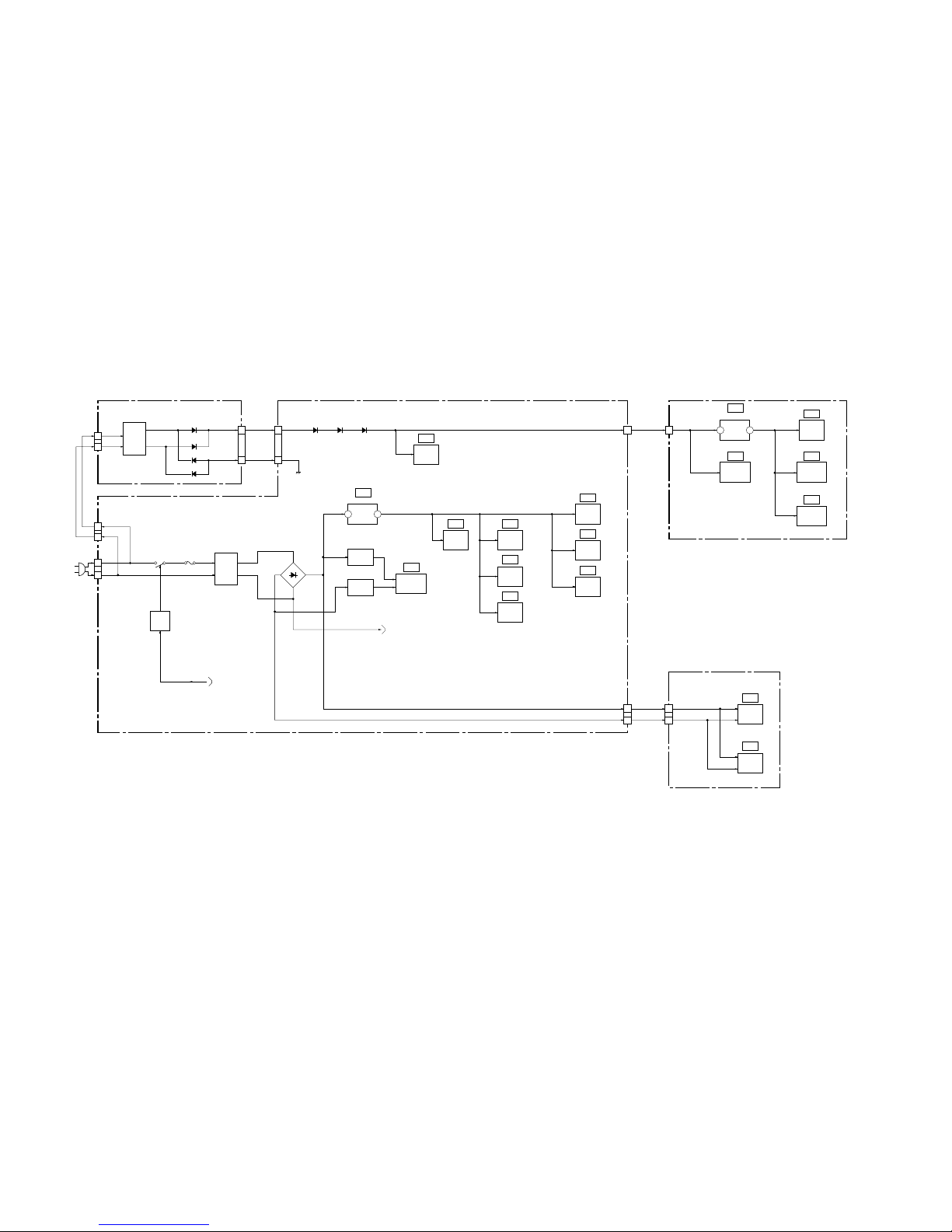
SA-F21
2-5 2-6 E
2-3. POWER BLOCK DIAGRAM
2
1
2
1
T802
SUB
POWER
TRANS
D811 D816 D815 D814
D812
D810
D813
2
1
2
1
CN806 CN805
SUB TRANSFORMER BOARD
(SEE PAGE 3-7)
CONTROL BOARD
(SEE PAGE 3-11)
MAIN BOARD
(SEE PAGE 3-7)
CN804
CN803
T801
MAIN
POWER
TRANS
2
1
CN801
AUDIO/CONTROL
(SEE PAGE 2-3)
Q802
RELAY
DRIVE
RY801 F801
+8V REG
1 3IN OUT
IC104
IC106
D801
LIMITER
AMP,
LPF
MIX,
HPF
SOUND
CONTROL
IC103
MIX
AMP
IC107
LINE
AMP
IC601
IC801
HEADPHONE
AMP
IC501
SYSTEM
CONTROL
IC105
POWER
AMP
IC301
POWER
AMP
IC401
IC101
IC802
IC109
AMP
HPF
VOLUME,
TONE
CONTROL
IC102
3
1
5
3
1
POWER BOARD
(SEE PAGE 3-15)
CN302
1 3IN OUT
+5V REG.
RESET
SIGNAL
GENERATOR
IC504
AUTO
POWER
DETECT
IC502
REMOTE
COMMANDER
RECEIVER
IC503
6
CN102
+VCC
+VSS
–VSS
AC IN
05
AUDIO/CONTROL
(SEE PAGE 2-3)
Q803
+11V REG
Q804
–11V REG
Page 8
3-1
SA-F21
SECTION 3
PRINTED WIRING BOARDS AND SCHEMATIC DIAGRAMS
THIS NOTE IS COMMON FOR PRINTED WIRING
BOARDS AND SCHEMATIC DIAGRAMS.
(In addition to this, the necessary note is printed
in each block.)
For printed wiring boards:
• X : indicates a lead wire mounted on the component
side.
• x : indicates a lead wire mounted on the printed side.
• b : Pattern from the side which enables seeing.
(The other layers’ patterns are not indicated.)
For schematic diagram:
• Caution when replacing chip parts.
New parts must be attached after removal of chip.
Be careful not to heat the minus side of tantalum capacitor,
because it is damaged by the heat.
• All resistors are in ohms, 1/
4
W (Chip resistors : 1/
10
W) unless otherwise specified.
kΩ : 1000Ω, MΩ : 1000kΩ.
• All capacitors are in µF unless otherwise noted. pF : µµF
50V or less are not indicated except for electrolytics and
tantalums.
• All variable and adjustable resistors ha ve characteristic curve
B, unless otherwise noted.
• 2 : nonflammable resistor.
• 5 : fusible resistor.
• C : panel designation.
• f : internal component.
• C : adjustment for repair.
• U : B+ Line.
• V : B– Line.
• Circled numbers refer to w aveforms.
• Voltages are dc between measurement point.
• V oltage and wavef orms are dc with respect to ground under
no-signal conditions.
• Readings are taken with a digital multimeter (DC 10MΩ).
• Voltage variations may be noted due to normal production
tolerances.
When indicating parts by reference
number, please include the board
name.
Note:
The components identified by mark 0 or dotted
line with mark 0 are critical for safety.
Replace only with part
number specified.
Note:
Les composants identifiés par
une marque 0 sont critiques
pour la sécurité.
Ne les remplacer que par une
pièce portant le numéro
spécifié.
• Abbreviation
CND : Canadian model
SP : Singapore model
Page 9
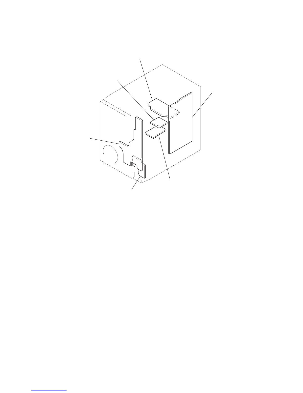
3-2
SA-F21
3-1. CIRCUIT BOARDS LOCATION
POWER board
SPEAKER TERMINAL board
CONTROL board
JACK board
SUB TRANSFORMER board
MAIN board
Page 10
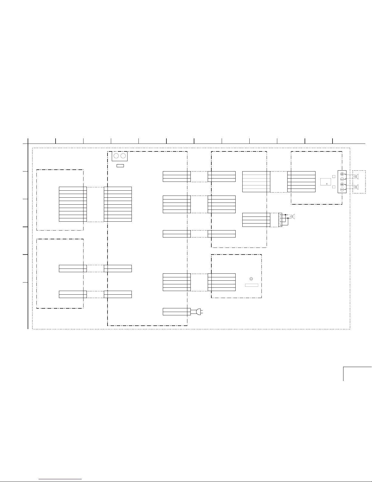
SA-F21
3-3
3-4
3-2. FRAME SCHEMATIC DIAGRAM
FRAME
6P
CN301
1L COLD
2L HOT
3R COLD
4R HOT
5ST RELAY-
6ST RELAY+
6P
CN305
1 L COLD
2 L HOT
3 R COLD
4 R HOT
5 ST RELAY-
6 ST RELAY+
5P
CN601
1 HP L
2 GND
3 HP R
4 MUTE
5 MUTE
5P
CN101
1HP L
2GND
3HP R
4MUTE
5MUTE
5P
CN303
1 L CH
2 GND
3 R CH
4SW
5 MUTE/STBY
5P
CN103
1L CH
2GND
3R CH
4SW
5MUTE/STBY
4P
CN304
1SW1+
2SW1-
3SW2+
4SW2-
3P
CN302
1 +VSS
2 GND
3 -VSS
3P
CN802
1+VSS
2GND
3-VSS
2P
CN308
1 RY CONT
2 ST RELAY-
2P
CN808
1RY CONT
2ST RELAY-
2P
CN806
1STBY VCC
2GND
2P
CN805
1 STBY VCC
2 GND
2P
CN804
1AC IN HOT
2AC IN COLD
2P
CN803
1 AC IN HOT
2 AC IN COLD
2P
CN801
1AC IN HOT
2AC IN COLD
10P
CN102
10 STANDBY
9 AUTO POWER DETECT
8 SW CLK
7 GND
6 GND
5 +VCC
4 SW DATA
3 VOL CE
2 VOL DATA
1 VOL CLK
10P
CN502
1STANDBY
2AUTO POWER DETECT
3SW CLK
4GND
5GND
6+VCC
7SW DATA
8VOL CE
9VOL DATA
10VOL CLK
1
A
R
4
SS-MS21
IMP
R-CH
SPEAKER
L-CH
L
J601
HEADPHONES
SPEAKER
TERMINAL
BOARD
JACK BOARD
POWER BOARD
TRANSFORMER
BOARD
PJ101
INPUT
MAIN BOARD
CONTROL BOARD
79
05
10
B
D
3
F
E
2
C
4 1185 126
SUB
LR
TM305
SS-82
SS-78
SS-83
SS-80
SS-79
SS-81
FFC-324
SA-WMS21
SUB WOOFER
SP101
SS-86
(SS-87)
Page 11
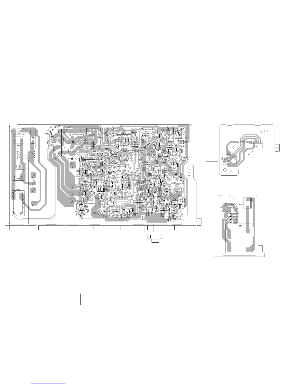
SA-F21
(11)
1-683-484-
11
JACK BOARD
HEADPHONES
J601
(11)
1-683-482-
A
B
C
1 2 3 4 5 6
7
11
05
MAIN BOARD
R L
PJ101
C
EB
BE
C
BE
C
C
EB
C
EB
16
1
32 17
C
EB
14
5
C
BE
C805
C
EB
C
EB
24 13
112
INPUT
C
EB
8
C811
(Singapore)
(11)
1-683-480-
11
SUB TRANSFORMER BOARD
3-5
3-6
3-3. PRINTED WIRING BOARDS AND SCHEMATIC DIAGRAMS
MAIN, JACK, SUB TRANSFORMER PRINTED WIRING BOARDS
– Ref. No. : MAIN board, JACK board, SUB TRANSFORMER board; 1,000 series –
MAIN, JACK, SUB TRANSFORMER
There are a few cases that the part isn't mounted in this model is printed on this diagram.
MAIN BOARD
CN101 B-3
CN102 A-5
CN801 B-1
CN805 A-4
D101 A-6
D103 B-6
D104 B-6
D105 A-6
D801 A-2
D806 B-4
D807 B-4
D808 A-2
D809 B-4
D814 A-5
D815 A-5
D816 A-4
IC101 C-5
IC102 C-4
IC103 C-6
IC104 C-6
IC105 B-6
IC106 B-7
IC107 C-6
IC109 B-6
IC601 C-4
IC801 A-5
Q101 A-6
Q102 A-5
Q601 B-4
Q602 C-3
Q603 B-3
Q604 C-3
Q605 C-3
Q802 A-2
Q803 B-4
Q804 B-3
Q805 A-7
Q806 A-4
Q807 A-7
Page 12

SA-F21
3-7
3-8
MAIN, JACK, SUB TRANSFORMER SCHEMATIC DIAGRAM
– Ref. No. : MAIN board, JACK board, SUB TRANSFORMER board; 1,000 series –
MAIN, JACK, SUB TRANSFORMER
B+
B+
B+
B+
B+
B+
B+
B+
B+
B+
B+
B+
B+
B+
B+ B+
B+
B+
B+
B+
B+
B+
B+
B+
B+
B+
B+
B+
B+
B+
B+
B+
B+
B-
B-
B-
B-
B-
B-
B-
B- B-
B-
B+
0
0
0
0
0
0
0
0
0
0
0
0
0
0
11.1
-11.1
0.5
0
4
4
4
4
4
4
7.9
4
7.9
4
4
4
4
4
4
4
7.9
4
4
4
7.9
4
4
4
4
4
4
4
4
7.9
4
4
10.4
5.2
5.2
5.2
4
4
4
5.2
5.2
5.2
0.7
0.8
1.3
0.8
8.7
-2.9
0
0
8.6
4.1
4.7
16.1
7.9
5
0.2
16.1
11.1
11.8
-11.8
-16.1
-11.1
0
3.7 0
3.7
7.5
3.7
0
3.7
3.7
0.2
0.3
0.5
3.7
3.7
3.7
3.7
3.93.9
3.8
3.9
3.9
3.7
3.9
3.9
3.9
3.9
0.8
1.8
1.8
0.8
0.1
1.1
3.9
3.7
3.9
3.9
3.9
3.9
3.9
3.8
7.3
3
7.8
(SP)
IC101
BH3854AFS
1
AGND2IN13NF14BVN15BIN16BVO17TIN18TVO19OUT110VCC11SC12INPUT13STBY14MUTE15P-CONT16DGND
17
VREF
18
LATCH
19
DATA
20
CLK
21BC22TC23VC24
OUT2
25
TVO2
26
TIN2
27
BVO2
28
BIN2
29
BVN2
30
NF2
31
IN2
32
FILTER
IC104 BH3864F
1234IN5
VCC
67
GND
89101112
13 14 15 16 17 18
DBC19SCK20SI21OUT
22 23 24
IC107(1/2)
NJM4580
3
2
1
IC103(1/2)
NJM4580
3
2
1
C155
22p
IC107(2/2)
NJM4580
5
6
8
7
4
IC103(2/2)
NJM4580
5
6
8
7
4
R110
100k
R101
6.8k
R102
33k
C101
100p
C103
4.7u
50V
PJ101
C153
4.7u
50V
C102
4.7u
50V
C202
4.7u
50V
C156
100u
16V
C157
0.1u
C120
10u
50V
C255
22p
R201
6.8k
R210
100k
C203
4.7u
50V
C201
100p
R202
33k
C253
4.7u 50V
R108
47k
C154
4.7u
50V
R208
47k
C254
4.7u
50V
C158
22p
R111
10k
C112
100p
C159
22p
R138
100k
C160
22p
C126
100u
16V
R133
10k
R125
10k
R126
10k
C136
100u
16V
C135
0.1u
R142
10
C163
100p
C104
0.068u
C105
0.068u
C106
0.015u
C121
1u
50V
C122
0.22u
C124
22u
50V
C125
10u
50V
C123
0.1u
C162
100p
C204
0.068u
C205
0.068u
C206
0.015u
R122
22
C128
100u
16V
R132
22
R123
100k
C129
0.22u
R124
100k
IC102(2/2)
NJM4580
5
6
8
7
4
IC102(1/2)
NJM4580
3
2
1
IC105(1/2)
NJM4580
3
2
1
R205
47k
R105
47k
R109
3.3k
C142
100p
C108
0.15u
C107
0.15u
R104
4.7k
C207
0.15u
C208
0.15u
R204
4.7k
R203
12k
R103
12k
C130
0.1u
C131
100u
16V
C141
100u
16V
C134
100u
16V
C139
0.1u
R136
0
C143
0.01u
C145
0.01u
C146
0.01u
R13022R131
22
R151
10k
R150
10k
C113
4.7u
50V
R112
100
C114
4.7u
50V
R113
4.7k
2P
CN804
2P
CN803
2P
CN801
2P
CN806
2P
CN805
D811
1SR139
D812 1SR139
D810 1SR139
D813
1SR139
C808
100u
25V
RY801
D808
1SS133
C807
0.01u
250V
C823
0.01u
F801
*
T801
3
2
14
5
6
1W
R806
220
C816
0.047u
C815
0.047u
R805
4.7
D816
1SS133
D815
1SS133
D814
1SS133
D801
RBV602
IC105(2/2)
NJM4580
5
6
8
7
4
IC106(1/2)
NJM4580
3
2
1
IC106(2/2)
NJM4580
5
6
8
7
4
C116
0.1u
C115
0.1u
R114
22k
R116
100k
R115
10k
R117
1k
R119
10k
C117
100p
R121
47k
R120
47k
C119
0.018u
C118
0.1u
C147
0.1u
C148
100u
16V
IC109(1/2)
NJM4580
3
2
1
IC109(2/2)
NJM4580
5
6
8
7
4
R206
2.2k
C209
4.7u
50V
C109
50V
4.7u
R106
2.2k
R107
4.7k
C110
330p
C149
0.1u
C150
100u
16V
R207
4.7k
C210 330p
C111
1u
50V
R620
10k
R609
4.7k
Q602
2SC3326
R611
10k
Q601
2SC3326
R621
10k
C211
1u
50V
R610
4.7k
R612
10k
R605
47k
C611
1u
50V
R602
1k
IC601(1/2)
NJM4556AD
3
2
1
C605
100p
IC601(2/2)
NJM4556AD
5
6
8
7
4
R607
47k
C612
1u
50V
C607
100p
R603
1k
R601
22k
C601
22p
C602
100u
16V
R604
22k
C603
22p
C610
0.1u
C609
16V
100u
C604
100u
16V
C606
0.1u
C608
100u
16V
Q604
2SC3326
Q603
2SC3326
R613
270
R606
1k
R615
10k
R614
270
R616
10k
R608
1k
5P
CN101
C613
220p
R617
2.7k
R619
22k
10P
CN102
R127
1k
R128
1k
R129
1k
R135 1k
C133
100p
C132
100p
C138
100p
C137
100p
R137
1k
C810
4700u
25V
5P
CN103
C161
10u
50V
R149
1k
D105
1SS133
D106
1SS133
D107
1SS133
Q101
2SC2412
R146
10k
R618
1k
R145
1k
R144
5.6k
R143
47k
C151
10u
50V
R139
10k
D101
1SS133
R140
1k
Q806
2SC2412
R813
10k
D809
1SS133
R809
47k
R810
47k
C824
50V
10u
C822
100u
16V
Q804
2SA954
Q803
2SC2003
D806
MTZJ12B
D807
MTZJ12B
C817
25V
47u
C818
47u
25V
R808
1.8k
C820
10u
50V
C819
10u
50V
R807
1.8k
C801
6800u
25V
C802
6800u
25V
C803
100u
25V
C804
0.1u
IC801
78MO8
123
C805
0.1u
C806
100u
25V
R80110R802
10k
C821
100u
16V
R803
10k
C809
100u
16V
3P
CN802
2P
CN808
Q805
2SC2412
Q807
2SC2003
R812
22k
R811
47k
1
A
C614
220p
5P
CN601
Q802
DTC124EK
Q102
DTC124EK
Q605
DTA124ES
C811
0.01u
250V
T802
HP R
4
HP L
5
3
MUTE
GND
2
MUTE
1
4
5
2
6
1
CLK
LATCH
SW DATA
GND
+VCC
GND
DATA
AUTO POWER DETECT
STANDBY
SW CLK
10
9
8
7
3
L CH
GND
4
1
MUTE/STBY
R CH
3
SW
5
2
GND
1
2
-VSS
3
+VSS
1
2
MAIN BOARD
IC101
VOLUME,TONE
SOUND CONTROL
IC104
IC102
HPF
MIX AMP
IC105
LPF
IC106
IC105
HPF
LIMITER AMP
IC106
IC801
+8V REGULATOR
IC601
HEADPHONE AMP
IC109
AMP
MIX AMP
IC103
LINE AMP
IC107
1
2
1
2
2
1
1
2
1
2
AC IN
790510
B
D
15 173 16
F
J
13
E
2
C
4 1185 12
H
G
14
I
6
CONTROL
(2/2)
(1/2)
(2/2)
(1/2)
MAIN POWER
TRANSFORMER
*F801
1.25A/250V(US,CND)
T500mA/250V(SP)
+11V REGULATOR
-11V REGULATOR
Q804
MUTING
POWER ON
Q806
Q805,807
CONTROL
RELAY
Q101,102
MUTE DRIVE
MUTE DRIVE
MUTE
MUTE
MUTE
MUTE
HP L
5
J601
HP R
4
MUTE
1
3
HEADPHONES
MUTE
GND
2
JACK BOARD
18
AUDIO
SIGNAL
SIGNAL PATH
PB
SUB
TRANSFORMER
BOARD
SUB POWER
TRANSFORMER
(SEE PAGE 3-12)
CONTROL BOARD
CN502
CN303
POWER BOARD
(SEE PAGE 3-15)
POWER BOARD
CN302
(SEE PAGE 3-15)
POWER BOARD
(SEE PAGE 3-16)
CN308
R
INPUT
L
Page 13
SA-F21
3-10
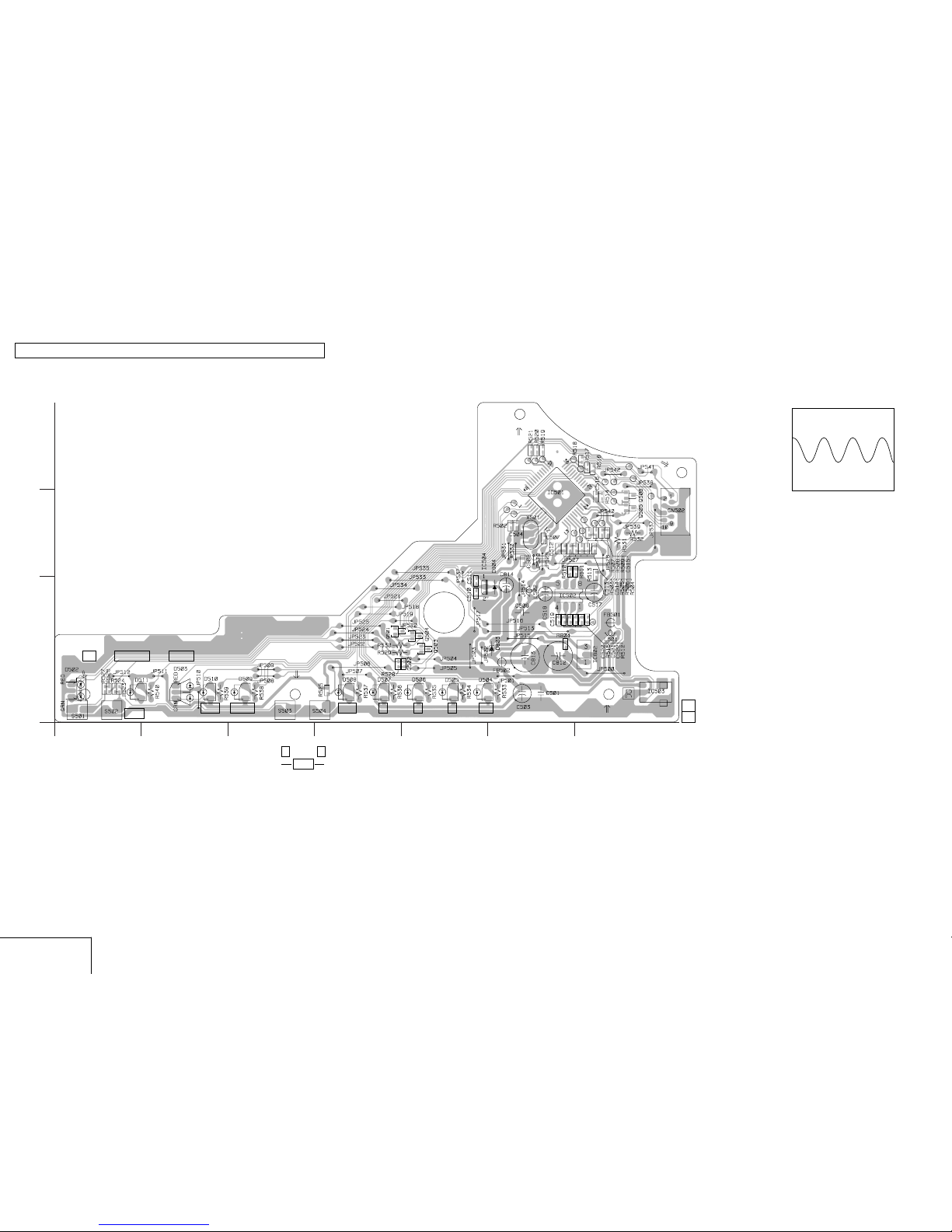
CONTROL PRINTED WIRING BOARD
– Ref. No. : CONTROL board; 1,000 series –
• Waveform
1 IC501 0
4.24 Vp-p
There are a few cases that the part isn't mounted in this model is printed on this diagram.
3-9
CONTROL
(11)
1-683-483-
A
B
C
1 2 3 4 5
6
7
11
05
CONTROL BOARD
I/1
S501, D502
MODE
MASTER VOL
D511
SW VOL
D503
BASS TREBLE
+
LEVEL
S503
–
S504
MAX 3 2 1 MIN
3
2
1
BE
C
BE
C
BE
C
BE
C
BE
C
CONTROL BOARD
CN502 B-7
D502 C-1
D503 C-2
D504 C-5
D505 C-5
D506 C-5
D507 C-4
D508 C-4
D509 C-3
D510 C-2
D511 C-1
D803 C-6
D804 B-6
IC501 B-6
IC502 C-6
IC503 C-7
IC504 B-5
IC802 C-7
Q501 C-4
Q503 C-5
Q504 C-5
Q505 B-7
Q506 B-7
Page 14
SA-F21
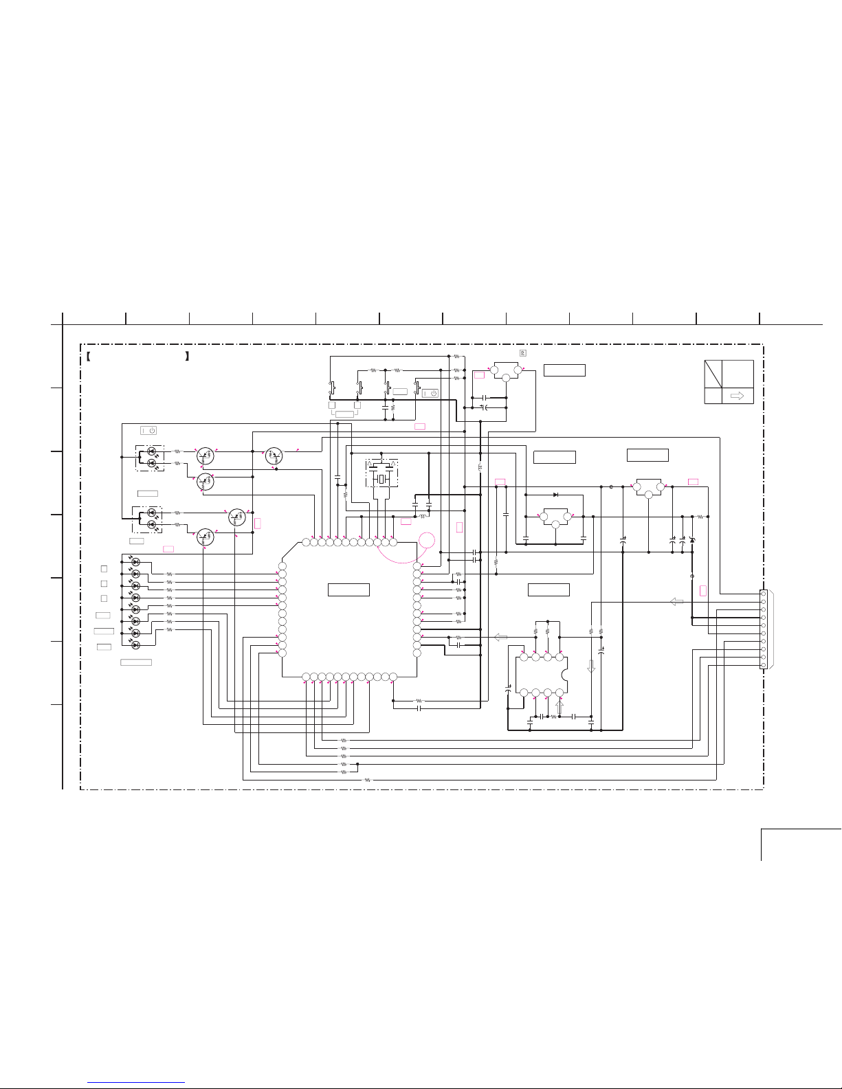
CONTROL SCHEMATIC DIAGRAM
– Ref. No. : CONTROL board; 1,000 series –
3-11
3-12
CONTROL
B+
B+
B+ B+
B+
B+
B+
B+
B+
55
5.7
5
5
10.1
5
0.1
5
0
5
5
5
0
5
0.1
5
4.9 5
5
0.1
5
5
5
5
5
5
0.1
5.7
0.4
4.3
4.3
4.3
4.3
0.4
0.1
0.6
1.2
0.214.1
4.1
0.6
55 5
5
0.1
0.1
55 5
2.2
2.6
5
0.2
0.1
4.2
4.2
0.5
0.3
0.4
1
IC501
LC865508A-5N93
1
NC
2
LED_STBY
3
LED_OPR
4
MAIN_SW
5
RESET
6
XT1
7NC8
XT2
9
VSS
10
CF1
11
CF2
12
VDD
13
KEY1
14
KEY2
15
VREF
161718
NC
19202122
AUTO SW
2324
NC
25
RIMOKON
26NC27NC28
MOVIE
29NC30
MUSIC31LED_VOL32LED_BASS33LED_TREBLE
34
VOL_DATA35VOL_CE
36
VOL_CLK
37
SW_DATA
38
SW_LATCH
39
SW_CLK
40
NC
41
NC
42
NC
43
LED_MAX
44
LED_LEVEL3
45
LED_LEVEL2
46
LED_LEVEL1
47
LED_MIN
48
NC
R505
47k
R506
47k
R507
47k
R508
47k
R509
47k
R533 270
R534
270
R535
270
R536
270
R537
270
R538
180
R539
180
R540 180
D504
SLR325DCT31
D505
SLR325DCT31
D506
SLR325DCT31
D507
SLR325DCT31
D508
SLR325DCT31
D509
SLR325MCT31
D510
SLR325MCT31
D511
SLR325MCT31
R532
180
D503
SPR-325MVWT
R531
470
D502
SPR-325MVWT
R529
180
R530
180
R516
4.7k
R517
4.7k
R518
4.7k
R519
10k
R520
10k
R521
1k
C515
0.1u
R514
47k
C516
100p
C514
0.1u
R503
100
R510
15k
R512
100
R513
1.2k
IC502
NJM2072
1
INPUT
2
GAIN
CONT3AMP
OUT
4
VEE
5
RECOVEIN
TIME CAP
6
OUTPUT1
7
OUTPUT2
8
VCC
C520
1000p
R515
10k
C518
1u
50V
C519
1000p
C522
1000p
C521
0.1u
C517
100u
16V
C513
0.01u
C512
0.01u
L502
10uH
X501
6MHz
R502
10k
C507
0.1u
C508
0.1u
C504
0.1u
S504
S503
S502
S501
C502
0.1u
R528
100k
R523
4.7k
R524
2.2k
R526
4.7k
R527
4.7k
R525
4.7k
IC503
NJL64H400A
123
C501
0.1u
C503
100u 16V
L501
10uH
IC504
PST600
123
R504
47k
C509
0.47u
C510
0.1u
D804
1SS133
C511
0.1u
IC802
BA178M05T
123
C813
470u
16V
C812
470u
16V
C814
10u
50V
D803
MTZJ9.1B
R804
10k
10P
CN502
1
A
R511
15k
FB501
1.1uH
FB502
1.1uH
Q503
DTA124XK
Q504
DTA124XK
Q505
DTA124XK
Q506
DTA124XK
Q501
DTA124EK
SYSTEM
IC501
REMOTE
IC503
+5V REGULATOR
IC802
RESET
IC504
IC502
AUTO POWER
1
6
2
5
4
3
7
8
9
10
STANDBY
AUTO POWER DETECT
GND
SW CLK
+VCC
GND
SW DATA
VOL CE
VOL CLK
VOL DATA
CONTROL BOARD
79
05
10
B
D
3
F
E
2
C
4 1185 12
G
6
OPR
STBY
MOVIE
MUSIC
CONTROL
RECEIVER
SIGNAL
GENERATOR
INOUT
GND
GND
DATA
+B
DETECTORCONTROL
/
MASTER VOL
SW VOL
2
3
1
BASS
TREBLE
MIN
MAX
/
MODE
+-
LEVEL
CN102
MAIN BOARD
(SEE PAGE 3-8)
LED DRIVE
Q503,504
RELAY CONTROL
LED DRIVE
Q505,506
AUDIO
SIGNAL
SIGNAL PATH
PB
Page 15
3-14
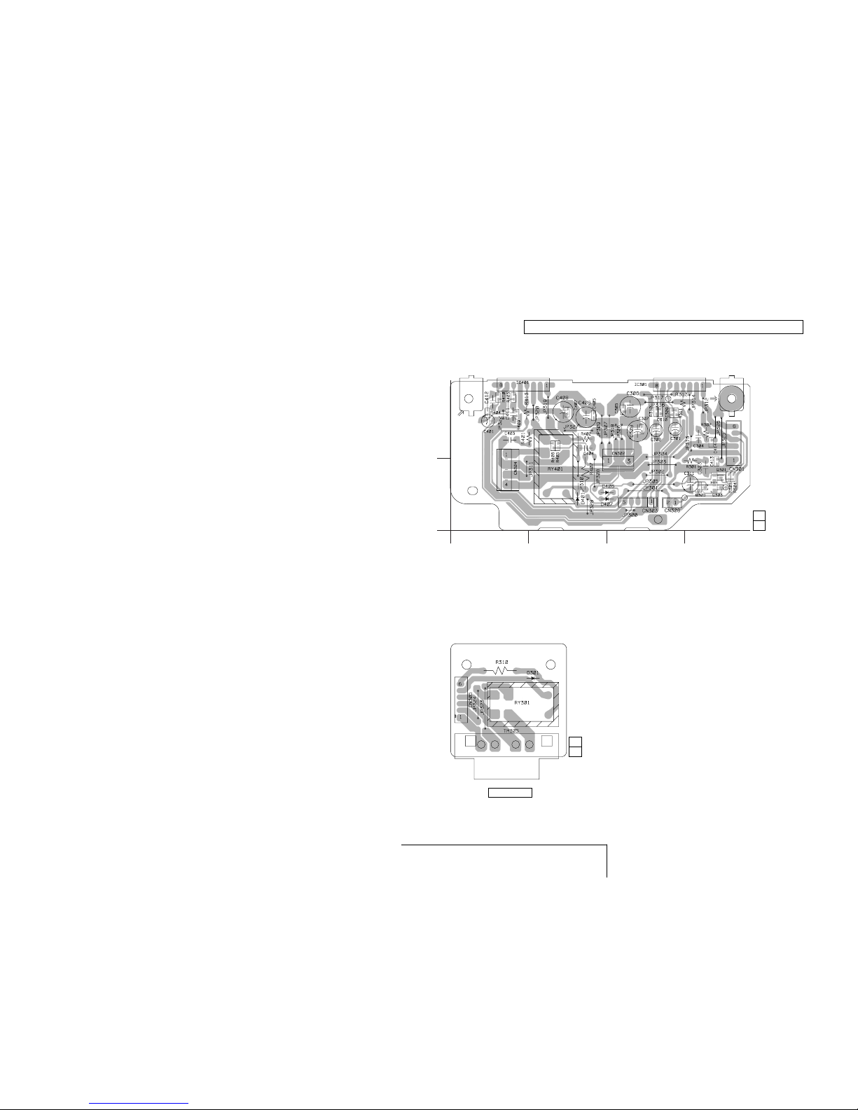
POWER, SPEAKER TERMINAL PRINTED WIRING BOARDS
– Ref. No. : POWER board, SPEAKER TERMINAL board; 1,000 series –
There are a few cases that the part isn't mounted in this model is printed on this diagram.
POWER, SPEAKER TERMINAL
POWER BOARD
CN301 A-4
CN302 A-3
CN303 B-3
CN304 B-1
CN308 B-3
D401 B-2
IC301 A-3
IC401 A-1
Q301 B-4
Q303 B-4
Q305 B-4
SA-F21
(11)
1-683-479-
A
B
1 2 3 4
11
05
POWER BOARD
B
E
C
E
C
B
E
C
B
(11)
1-683-481-
11
SPEAKER TERMINAL BOARD
SPEAKER IMP 4Ω
TM305
+
–
+
–
Page 16
SA-F21
3-15
3-16 E
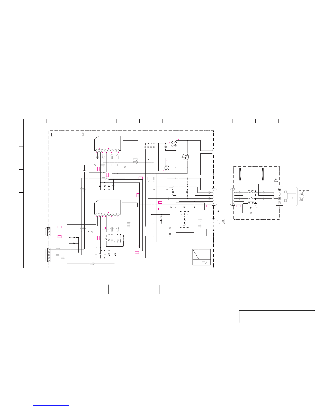
POWER, SPEAKER TERMINAL SCHEMATIC DIAGRAM
– Ref. No. : POWER board, SPEAKER TERMINAL board; 1,000 series –
POWER, SPEAKER TERMINAL
The components identified by mark 0 or dotted
line with mark 0 are critical for safety.
Replace only with part number specified.
Les composants identifiés par une marque 0 sont
critiques pour la sécurité. Ne les remplacer que
par une pièce portant le numéro spécifié.
B+
B+
B+
B+
B+
B-
B-
B-
B-
B+ B+
B+
B+
B-
0
8.7
8.7
8.6
0
0
16.1
0
8.5
-16.1
00
0
-16.1
00
8.5
0
16.1
IC301
TDA7264
1
OUT R2+VCC3OUT L4M/S5-VCC6IN L7SGND8IN R
IC401
TDA7264
1
OUT22+VCC3OUT14M/S5-VCC6IN17SGND8IN2
2P
CN308
6P
CN301
4P
CN304
5P
CN303
3P
CN302
6P
CN305
C309
100p
C310
100p
R311
1k
R312
1k
C302
1u
50V
R405
22k
R304
22k
R406
22k
R305
22k
C311
220u
10V
2SC2412
Q303
R313
1k
C301
1u
50V
C305
0.1u
C306
100u
25V
C307
0.1u
C308
100u
25V
R413
1k
C412
3300p
C411
3300p
R410
10k
R409
10k
R404
4.7k
C401
1u
50V
R403
4.7K
R301
10
C303
0.047u
C304
0.047u
R302
10
C413
0.01u
C414
0.01u
D401
1SS133
1W
R407
100
D406
1SS133
D407
1SS133
R401
10
C403
0.047u
C404
0.047u
R402
10
C408
100u
25V
C407
0.1u
C405
0.1u
RY401
RY301
D301
1SS133
1W
R310
100
1
A
C406
100u
25V
TM305
4P
Q301
DTC124EK
Q305
DTA124EK
RED
BLACK
BLACK
RED
IC301
POWER AMP
POWER AMP
IC401
1
2
2
1
3
4
5
6
4
1
6
5
2
3
4
1
2
3
3
2
5
4
1
3
2
1
GND
L CH
R CH
SWF
STBY/MUTE
GND
+VSS
-VSS
790510
B
D
3
F
E
2
C
4 1185 126
POWER BOARD
SPEAKER
TERMINAL
BOARD
SIGNAL PATH
SIGNAL
PB
AUDIO
SP101
SUB WOOFER
CN808
MAIN BOARD
(SEE PAGE 3-8)
Q301,303,305
RELAY
CONTROL
L-CH
R-CH
SS-MS21
R
L
SPEAKER
IMP
4
MAIN BOARD
CN802
(SEE PAGE 3-8)
CN103
MAIN BOARD
(SEE PAGE 3-8)
(CHASSIS)
Page 17
4-1
NOTE:
• -XX and -X mean standardized parts, so they may
have some difference from the original one.
• Items marked “*” are not stocked since they are
seldom required for routine service. Some delay
should be anticipated when ordering these items.
• The mechanical parts with no reference number in
the exploded views are not supplied.
• Hardware (# mark) list and accessories and packing materials are given in the last of the electrical
parts list.
SECTION 4
REPAIR PARTS LIST
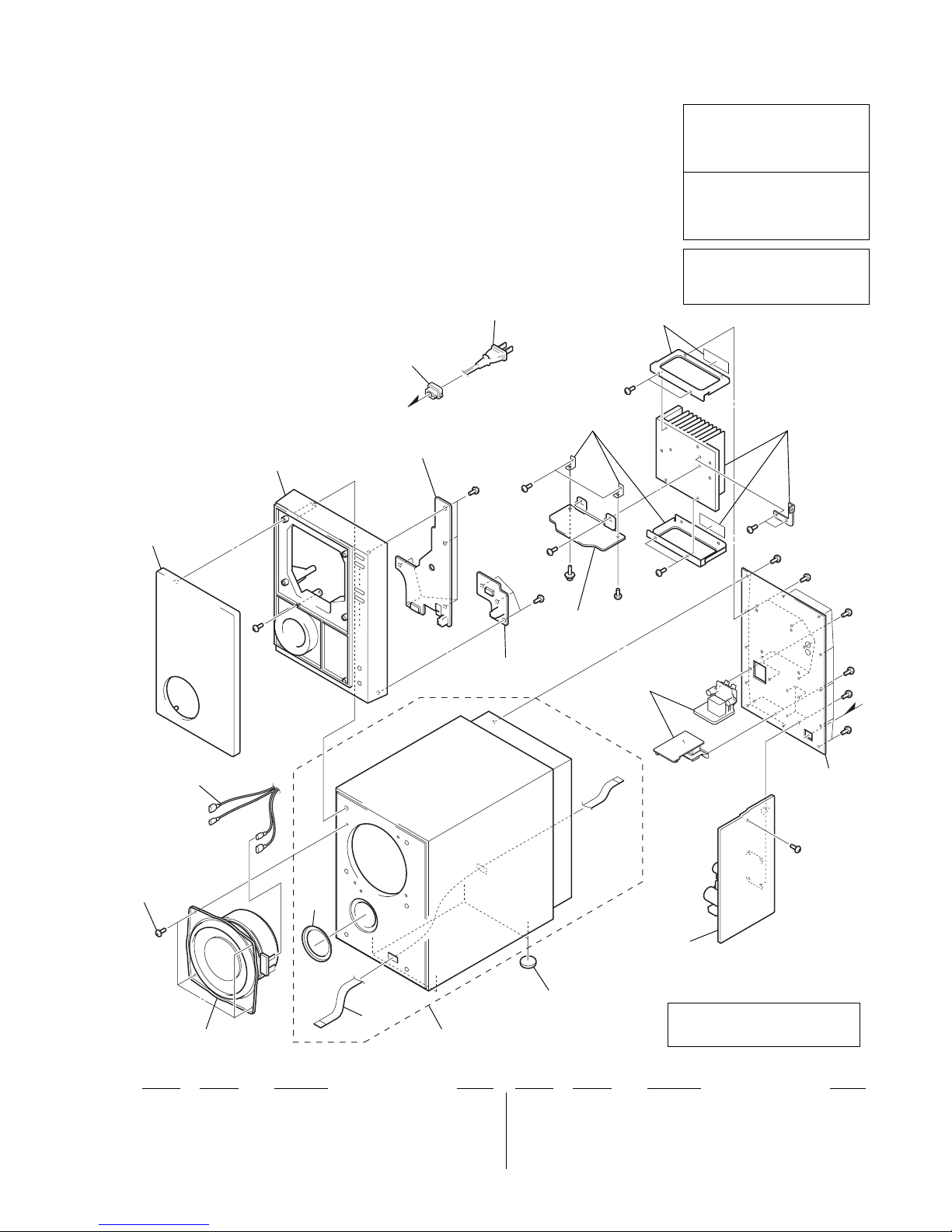
4-1. EXPLODED VIEWS
SA-F21
The components identified by mark
0 or dotted line with mark 0 are
critical for safety.
Replace only with part number specified.
Les composants identifiés par une
marque 0 sont critiquens pour la
sécurité.
Ne les remplacer que par une pièce
portant le numéro spécifié.
4-1-1. SA-WMS21
1
6
7
8
2
3
4
5
#1
#2
#5
#5
#5
#5
#5
#1
#1
#2
#2
#5
#
4
#4
#2
#3
#5
SP101
not supplied
not supplied
not supplied
not suppliednot supplied
not
supplied
not
supplied
not supplied
not supplied
not supplied
not
supplied
Ref. No. Part No. Description RemarkRef. No. Part No. Description Remark
0 5 1-792-211-11 CORD, POWER (US, Canadian)
6 A-6062-690-A ENCLOSER BLOCK ASSY
7 3-072-108-01 SEAL (DUCT)
8 1-823-567-11 CABLE, FLEXIBLE FLAT (FFC-324)
SP101 1-544-991-11 SPEAKER (13 cm)
1 3-072-126-01 +B TAPPING SCREW 4 MAIN 4X20
2 X-3952-072-1 GRILLE ASSY
3 A-6062-691-A PANEL BLOCK ASSY, FRONT
4 3-072-094-01 BUSHING, CODE
0 5 1-769-744-11 CORD, POWER (Singapore)
SA-WMS21 is a two-channel speaker.
Make it sure to plug in the speaker
cord to two Ls and two Rs when the
speaker is replaced.
Use bond to put the grille assy, the
panel block assy, and the encloser
block assy together.
Page 18
4-2
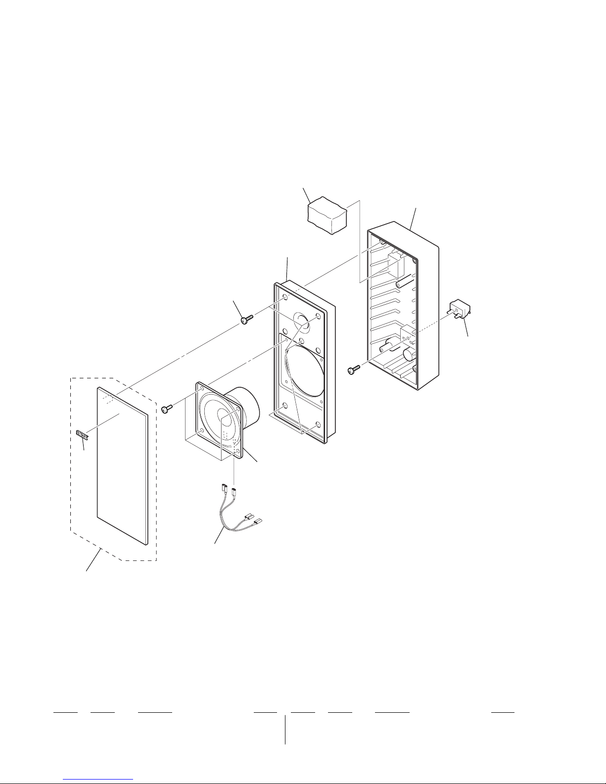
4-1-2. SS-MS21
Ref. No. Part No. Description RemarkRef. No. Part No. Description Remark
54 3-072-121-01 CASE, FRONT
55 A-6062-694-A CASE (S) BLOCK ASSY, REAR
SP201 1-544-990-11 SPEAKER (8 cm)
51 X-3952-073-1 GRILLE (S) ASSY
52 3-072-124-01 SONY BADGE
53 3-072-127-01 +P TAPPING SCREW 3.5X16 CZN
51
52
#2
#2
not supplied
SP201
53
54
55
not supplied
not supplie
d
Page 19
4-3
NOTE:
• Due to standardization, replacements in the
parts list may be different from the parts specified in the diagrams or the components used
on the set.
• -XX and -X mean standardized parts, so they
may have some difference from the original
one.
• RESISTORS
All resistors are in ohms.
METAL: Metal-film resistor.
METAL OXIDE: Metal o xide-film resistor.
F: nonflammable
• Items marked “*” are not stocked since they
are seldom required for routine service.
Some delay should be anticipated when ordering these items.
• SEMICONDUCTORS
In each case, u: µ, for example:
uA. . : µA. . uPA. . : µPA. .
uPB. . : µPB. . uPC. . : µPC. .
uPD. . : µPD. .
• CAPACITORS
uF: µF
• COILS
uH: µH
4-2. ELECTRICAL PARTS LIST
Ref. No. Part No. Description Remark Ref. No. Part No. Description Remark
Les composants identifiés par une
marque 0 sont critiquens pour la
sécurité.
Ne les remplacer que par une pièce
portant le numéro spécifié.
The components identified by
mark 0 or dotted line with mark
0 are critical for safety.
Replace only with part number
specified.
When indicating parts by reference
number, please include the board.
CONTROL
CONTROL BOARD
**************
(Ref.No.1,000 Series)
< CAPACITOR >
C501 1-164-303-51 CERAMIC 0.1uF 25V
C502 1-164-156-11 CERAMIC CHIP 0.1uF 25V
C503 1-126-382-11 ELECT 100uF 20% 16V
C504 1-164-156-11 CERAMIC CHIP 0.1uF 25V
C507 1-164-156-11 CERAMIC CHIP 0.1uF 25V
C508 1-164-156-11 CERAMIC CHIP 0.1uF 25V
C509 1-137-194-91 FILM 0.47uF 5% 50V
C510 1-164-156-11 CERAMIC CHIP 0.1uF 25V
C511 1-164-156-11 CERAMIC CHIP 0.1uF 25V
C512 1-162-970-11 CERAMIC CHIP 0.01uF 10% 25V
C513 1-162-970-11 CERAMIC CHIP 0.01uF 10% 25V
C514 1-164-156-11 CERAMIC CHIP 0.1uF 25V
C515 1-164-156-11 CERAMIC CHIP 0.1uF 25V
C516 1-162-927-11 CERAMIC CHIP 100PF 5% 50V
C517 1-126-382-11 ELECT 100uF 20% 16V
C518 1-104-942-11 ELECT 1uF 20% 50V
C519 1-162-964-11 CERAMIC CHIP 0.001uF 10% 50V
C520 1-162-964-11 CERAMIC CHIP 0.001uF 10% 50V
C521 1-164-156-11 CERAMIC CHIP 0.1uF 25V
C522 1-162-964-11 CERAMIC CHIP 0.001uF 10% 50V
C812 1-126-941-11 ELECT 470uF 20% 16V
C813 1-126-941-11 ELECT 470uF 20% 16V
C814 1-124-261-00 ELECT 10uF 20% 50V
< CONNECTOR >
* CN502 1-784-732-11 CONNECTOR, FFC 10P
< DIODE >
D502 8-719-064-11 DIODE SPR-325MVW (I/1)
D503 8-719-064-11 DIODE SPR-325MVW (SW VOL)
D504 8-719-063-91 DIODE SLR325DC-P-T32 (MIN)
D505 8-719-063-91 DIODE SLR325DC-P-T32 (1)
D506 8-719-063-91 DIODE SLR325DC-P-T32 (2)
D507 8-719-063-91 DIODE SLR325DC-P-T32 (3)
D508 8-719-063-91 DIODE SLR325DC-P-T32 (MAX)
D509 8-719-063-92 DIODE SLR325MC-M-T31-NP (TREBLE)
D510 8-719-063-92 DIODE SLR325MC-M-T31-NP (BASS)
D511 8-719-063-92 DIODE SLR325MC-M-T31-NP (MASTER VOL)
D803 8-719-929-15 DIODE MTZJ-T-77-9.1B
D804 8-719-991-33 DIODE 1SS133T-77
< FERRITE BEAD >
FB501 1-410-397-21 FERRITE BEAD INDUCTOR
FB502 1-410-397-21 FERRITE BEAD INDUCTOR
< IC >
IC501 6-801-046-01 IC LC865508A-5N93
IC502 8-759-701-55 IC NJM2072D
IC503 8-759-459-86 IC NJL64H400A
IC504 8-759-165-81 IC PST600D-T
IC802 8-759-938-15 IC BA178M05T
< COIL >
L501 1-410-509-11 INDUCTOR 10uH
L502 1-410-509-11 INDUCTOR 10uH
< TRANSISTOR >
Q501 8-729-027-31 TRANSISTOR DTA124EKA-T146
Q503 8-729-027-33 TRANSISTOR DTA124XKA-T146
Q504 8-729-027-33 TRANSISTOR DTA124XKA-T146
Q505 8-729-027-33 TRANSISTOR DTA124XKA-T146
Q506 8-729-027-33 TRANSISTOR DTA124XKA-T146
< RESISTOR >
R502 1-216-833-11 METAL CHIP 10K 5% 1/16W
R503 1-216-809-11 METAL CHIP 100 5% 1/16W
R504 1-216-841-11 METAL CHIP 47K 5% 1/16W
R505 1-216-841-11 METAL CHIP 47K 5% 1/16W
R506 1-216-841-11 METAL CHIP 47K 5% 1/16W
R507 1-216-841-11 METAL CHIP 47K 5% 1/16W
R508 1-216-841-11 METAL CHIP 47K 5% 1/16W
R509 1-216-841-11 METAL CHIP 47K 5% 1/16W
R510 1-216-835-11 METAL CHIP 15K 5% 1/16W
R511 1-216-835-11 METAL CHIP 15K 5% 1/16W
R512 1-216-809-11 METAL CHIP 100 5% 1/16W
R513 1-216-822-11 METAL CHIP 1.2K 5% 1/16W
R514 1-216-841-11 METAL CHIP 47K 5% 1/16W
R515 1-216-833-11 METAL CHIP 10K 5% 1/16W
R516 1-216-829-11 METAL CHIP 4.7K 5% 1/16W
R517 1-216-829-11 METAL CHIP 4.7K 5% 1/16W
Page 20
4-4
Ref. No. Part No. Description Remark Ref. No. Part No. Description Remark
CONTROL JACK MAIN
R518 1-216-829-11 METAL CHIP 4.7K 5% 1/16W
R519 1-216-833-11 METAL CHIP 10K 5% 1/16W
R520 1-216-833-11 METAL CHIP 10K 5% 1/16W
R521 1-216-821-11 METAL CHIP 1K 5% 1/16W
R523 1-216-829-11 METAL CHIP 4.7K 5% 1/16W
R524 1-216-825-11 METAL CHIP 2.2K 5% 1/16W
R525 1-216-829-11 METAL CHIP 4.7K 5% 1/16W
R526 1-216-829-11 METAL CHIP 4.7K 5% 1/16W
R527 1-216-829-11 METAL CHIP 4.7K 5% 1/16W
R528 1-216-845-11 METAL CHIP 100K 5% 1/16W
R529 1-249-408-11 CARBON 180 5% 1/4W
R530 1-249-413-11 CARBON 470 5% 1/4W
R531 1-249-413-11 CARBON 470 5% 1/4W
R532 1-249-408-11 CARBON 180 5% 1/4W
R533 1-249-410-11 CARBON 270 5% 1/4W
R534 1-249-410-11 CARBON 270 5% 1/4W
R535 1-249-410-11 CARBON 270 5% 1/4W
R536 1-249-410-11 CARBON 270 5% 1/4W
R537 1-249-410-11 CARBON 270 5% 1/4W
R538 1-249-408-11 CARBON 180 5% 1/4W
R539 1-249-408-11 CARBON 180 5% 1/4W
R540 1-249-408-11 CARBON 180 5% 1/4W
R804 1-216-833-11 METAL CHIP 10K 5% 1/16W
< SWITCH >
S501 1-771-349-21 SWITCH, KEYBOARD (I/1)
S502 1-771-349-21 SWITCH, KEYBOARD (MODE)
S503 1-771-349-21 SWITCH, KEYBOARD (LEVEL +)
S504 1-771-349-21 SWITCH, KEYBOARD (LEVEL -)
< VIBRATOR >
X501 1-577-360-11 VIBRATOR, CERAMIC (6MHz)
JACK BOARD
***********
(Ref.No.1,000 Series)
< CONNECTOR >
* CN601 1-564-520-11 PLUG, CONNECTOR 5P
< JACK >
J601 1-816-209-11 JACK, MINIATURE (HEADPHONES)
MAIN BOARD
***********
(Ref.No.1,000 Series)
1-533-233-11 HOLDER, FUSE
< CAPACITOR >
C101 1-162-927-11 CERAMIC CHIP 100PF 5% 50V
C102 1-126-963-11 ELECT 4.7uF 20% 50V
C103 1-126-963-11 ELECT 4.7uF 20% 50V
C104 1-130-493-00 MYLAR 0.068uF 5% 50V
C105 1-130-493-00 MYLAR 0.068uF 5% 50V
C106 1-130-485-00 MYLAR 0.015uF 5% 50V
C107 1-130-497-00 MYLAR 0.15uF 5% 50V
C108 1-130-497-00 MYLAR 0.15uF 5% 50V
C109 1-126-963-11 ELECT 4.7uF 20% 50V
C110 1-162-959-11 CERAMIC CHIP 330PF 5% 50V
C111 1-124-903-11 ELECT 1uF 20% 50V
C112 1-162-927-11 CERAMIC CHIP 100PF 5% 50V
C113 1-126-963-11 ELECT 4.7uF 20% 50V
C114 1-126-963-11 ELECT 4.7uF 20% 50V
C115 1-130-495-00 MYLAR 0.1uF 5% 50V
C116 1-130-495-00 MYLAR 0.1uF 5% 50V
C117 1-162-927-11 CERAMIC CHIP 100PF 5% 50V
C118 1-130-495-00 MYLAR 0.1uF 5% 50V
C119 1-136-156-00 MYLAR 0.018uF 5% 50V
C120 1-126-964-11 ELECT 10uF 20% 50V
C121 1-124-903-11 ELECT 1uF 20% 50V
C122 1-130-499-00 MYLAR 0.22uF 5% 50V
C123 1-164-156-11 CERAMIC CHIP 0.1uF 25V
C124 1-126-965-11 ELECT 22uF 20% 50V
C125 1-126-964-11 ELECT 10uF 20% 50V
C126 1-104-665-11 ELECT 100uF 20% 16V
C128 1-104-665-11 ELECT 100uF 20% 16V
C129 1-130-499-00 MYLAR 0.22uF 5% 50V
C130 1-164-156-11 CERAMIC CHIP 0.1uF 25V
C131 1-104-665-11 ELECT 100uF 20% 16V
C132 1-162-927-11 CERAMIC CHIP 100PF 5% 50V
C133 1-162-927-11 CERAMIC CHIP 100PF 5% 50V
C134 1-104-665-11 ELECT 100uF 20% 16V
C135 1-164-156-11 CERAMIC CHIP 0.1uF 25V
C136 1-104-665-11 ELECT 100uF 20% 16V
C137 1-162-927-11 CERAMIC CHIP 100PF 5% 50V
C138 1-162-927-11 CERAMIC CHIP 100PF 5% 50V
C139 1-164-156-11 CERAMIC CHIP 0.1uF 25V
C141 1-104-665-11 ELECT 100uF 20% 16V
C142 1-162-927-11 CERAMIC CHIP 100PF 5% 50V
C143 1-162-970-11 CERAMIC CHIP 0.01uF 10% 25V
C145 1-164-156-11 CERAMIC CHIP 0.1uF 25V
C146 1-162-970-11 CERAMIC CHIP 0.01uF 10% 25V
C147 1-164-156-11 CERAMIC CHIP 0.1uF 25V
C148 1-104-665-11 ELECT 100uF 20% 16V
C149 1-164-156-11 CERAMIC CHIP 0.1uF 25V
C150 1-104-665-11 ELECT 100uF 20% 16V
C151 1-126-964-11 ELECT 10uF 20% 50V
C153 1-126-963-11 ELECT 4.7uF 20% 50V
C154 1-126-963-11 ELECT 4.7uF 20% 50V
C155 1-162-919-11 CERAMIC CHIP 22PF 5% 50V
C156 1-104-665-11 ELECT 100uF 20% 16V
C157 1-164-156-11 CERAMIC CHIP 0.1uF 25V
C158 1-162-919-11 CERAMIC CHIP 22PF 5% 50V
C159 1-162-919-11 CERAMIC CHIP 22PF 5% 50V
C160 1-162-919-11 CERAMIC CHIP 22PF 5% 50V
C161 1-126-964-11 ELECT 10uF 20% 50V
C162 1-162-927-11 CERAMIC CHIP 100PF 5% 50V
C163 1-162-927-11 CERAMIC CHIP 100PF 5% 50V
C201 1-162-927-11 CERAMIC CHIP 100PF 5% 50V
C202 1-126-963-11 ELECT 4.7uF 20% 50V
C203 1-126-963-11 ELECT 4.7uF 20% 50V
C204 1-130-493-00 MYLAR 0.068uF 5% 50V
C205 1-130-493-00 MYLAR 0.068uF 5% 50V
C206 1-130-485-00 MYLAR 0.015uF 5% 50V
C207 1-130-497-00 MYLAR 0.15uF 5% 50V
C208 1-130-497-00 MYLAR 0.15uF 5% 50V
C209 1-126-963-11 ELECT 4.7uF 20% 50V
C210 1-162-959-11 CERAMIC CHIP 330PF 5% 50V
C211 1-124-903-11 ELECT 1uF 20% 50V
Page 21
4-5
Ref. No. Part No. Description Remark Ref. No. Part No. Description Remark
MAIN
C253 1-126-963-11 ELECT 4.7uF 20% 50V
C254 1-126-963-11 ELECT 4.7uF 20% 50V
C255 1-162-919-11 CERAMIC CHIP 22PF 5% 50V
C601 1-162-919-11 CERAMIC CHIP 22PF 5% 50V
C602 1-104-665-11 ELECT 100uF 20% 16V
C603 1-162-919-11 CERAMIC CHIP 22PF 5% 50V
C604 1-104-665-11 ELECT 100uF 20% 16V
C605 1-162-927-11 CERAMIC CHIP 100PF 5% 50V
C606 1-164-156-11 CERAMIC CHIP 0.1uF 25V
C607 1-162-927-11 CERAMIC CHIP 100PF 5% 50V
C608 1-104-665-11 ELECT 100uF 20% 16V
C609 1-104-665-11 ELECT 100uF 20% 16V
C610 1-164-156-11 CERAMIC CHIP 0.1uF 25V
C611 1-124-903-11 ELECT 1uF 20% 50V
C612 1-124-903-11 ELECT 1uF 20% 50V
C613 1-164-230-11 CERAMIC CHIP 220PF 5% 50V
C614 1-164-230-11 CERAMIC CHIP 220PF 5% 50V
C801 1-126-946-11 ELECT 6800uF 20% 25V
C802 1-126-946-11 ELECT 6800uF 20% 25V
C803 1-104-665-11 ELECT 100uF 20% 25V
C804 1-164-156-11 CERAMIC CHIP 0.1uF 25V
C805 1-164-156-11 CERAMIC CHIP 0.1uF 25V
C806 1-104-665-11 ELECT 100uF 20% 25V
0 C807 1-113-925-11 CERAMIC 0.01uF 20% 250V
C809 1-104-665-11 ELECT 100uF 20% 16V
C810 1-128-548-11 ELECT 4700uF 20% 25V
0 C811 1-113-925-11 CERAMIC 0.01uF 20% 250V
C815 1-130-491-00 MYLAR 0.047uF 5% 50V
C816 1-130-491-00 MYLAR 0.047uF 5% 50V
C817 1-126-947-11 ELECT 47uF 20% 25V
C818 1-126-947-11 ELECT 47uF 20% 25V
C819 1-126-964-11 ELECT 10uF 20% 50V
C820 1-126-964-11 ELECT 10uF 20% 50V
C821 1-104-665-11 ELECT 100uF 20% 16V
C822 1-104-665-11 ELECT 100uF 20% 16V
0 C823 1-113-925-11 CERAMIC 0.01uF 20% 250V
C824 1-126-964-11 ELECT 10uF 20% 50V
< CONNECTOR >
* CN101 1-564-508-11 PLUG, CONNECTOR 5P
CN102 1-695-371-31 CONNECTOR, FFC 10P
0 CN801 1-564-321-00 PIN, CONNECTOR 2P
* CN805 1-506-944-11 PIN, CONNECTOR 2P
< DIODE >
D101 8-719-991-33 DIODE 1SS133T-77
D105 8-719-991-33 DIODE 1SS133T-77
D106 8-719-991-33 DIODE 1SS133T-77
D107 8-719-991-33 DIODE 1SS133T-77
D801 8-719-302-37 DIODE RBV-602
D806 8-719-110-31 DIODE MTZJ-T-77-12B
D807 8-719-110-31 DIODE MTZJ-T-77-12B
D808 8-719-991-33 DIODE 1SS133T-77
D809 8-719-991-33 DIODE 1SS133T-77
D814 8-719-991-33 DIODE 1SS133T-77
D815 8-719-991-33 DIODE 1SS133T-77
D816 8-719-991-33 DIODE 1SS133T-77
< FUSE >
0 F801 1-532-389-31 FUSE, GLASS CYLINDERICAL
(T500mAL/250V) (Singapore)
0 F801 1-533-540-11 FUSE, GLASS CYLINDERICAL (1.25A/250V)
(US, Canadian)
< IC >
IC101 8-759-540-49 IC BH3854AFS
IC102 8-759-656-83 IC NJM4580MD- (TE2)
IC103 8-759-656-83 IC NJM4580MD- (TE2)
IC104 8-759-671-15 IC BH3864F
IC105 8-759-656-83 IC NJM4580MD- (TE2)
IC106 8-759-656-83 IC NJM4580MD- (TE2)
IC107 8-759-656-83 IC NJM4580MD- (TE2)
IC109 8-759-656-83 IC NJM4580MD- (TE2)
IC601 8-759-356-16 IC NJM4556AD
IC801 8-759-701-58 IC NJM78M08FA
< JACK >
PJ101 1-816-208-11 JACK, PIN (INPUT)
< TRANSISTOR >
Q101 8-729-120-28 TRANSISTOR 2SC2412K-T-146-QR
Q102 8-729-901-00 TRANSISTOR DTC124EKA-T146
Q601 8-729-202-38 TRANSISTOR 2SC3326N-TE85L-B
Q602 8-729-202-38 TRANSISTOR 2SC3326N-TE85L-B
Q603 8-729-202-38 TRANSISTOR 2SC3326N-TE85L-B
Q604 8-729-202-38 TRANSISTOR 2SC3326N-TE85L-B
Q605 8-729-027-31 TRANSISTOR DTA124EKA-T146
Q802 8-729-901-00 TRANSISTOR DTC124EKA-T146
Q803 1-800-937-11 TRANSISTOR 2SC2003
Q804 1-800-938-11 TRANSISTOR 2SA954
Q805 8-729-120-28 TRANSISTOR 2SC2412K-T-146-QR
Q806 8-729-120-28 TRANSISTOR 2SC2412K-T-146-QR
Q807 1-800-937-11 TRANSISTOR 2SC2003
< RESISTOR >
R101 1-216-831-11 METAL CHIP 6.8K 5% 1/16W
R102 1-216-839-11 METAL CHIP 33K 5% 1/16W
R103 1-216-834-11 METAL CHIP 12K 5% 1/16W
R104 1-216-829-11 METAL CHIP 4.7K 5% 1/16W
R105 1-216-841-11 METAL CHIP 47K 5% 1/16W
R106 1-216-825-11 METAL CHIP 2.2K 5% 1/16W
R107 1-216-829-11 METAL CHIP 4.7K 5% 1/16W
R108 1-216-841-11 METAL CHIP 47K 5% 1/16W
R109 1-216-827-11 METAL CHIP 3.3K 5% 1/16W
R110 1-216-845-11 METAL CHIP 100K 5% 1/16W
R111 1-216-833-11 METAL CHIP 10K 5% 1/16W
R112 1-216-809-11 METAL CHIP 100 5% 1/16W
R113 1-216-829-11 METAL CHIP 4.7K 5% 1/16W
R114 1-216-837-11 METAL CHIP 22K 5% 1/16W
R115 1-216-833-11 METAL CHIP 10K 5% 1/16W
R116 1-216-845-11 METAL CHIP 100K 5% 1/16W
R117 1-216-821-11 METAL CHIP 1K 5% 1/16W
R119 1-216-833-11 METAL CHIP 10K 5% 1/16W
R120 1-216-841-11 METAL CHIP 47K 5% 1/16W
R121 1-216-841-11 METAL CHIP 47K 5% 1/16W
The components identified by
mark 0 or dotted line with
mark 0 are critical for safety .
Replace only with part number specified.
Les composants identifiés par une
marque 0 sont critiques pour la
sécurité.
Ne les remplacer que par une pièce
portant le numéro spécifié.
Page 22
4-6
Ref. No. Part No. Description Remark Ref. No. Part No. Description Remark
R803 1-249-429-11 CARBON 10K 5% 1/4W
R805 1-249-386-11 CARBON 4.7 5% 1/6W
R806 1-215-865-11 METAL OXIDE 220 5% 1W
R807 1-249-420-11 CARBON 1.8K 5% 1/4W
R808 1-249-420-11 CARBON 1.8K 5% 1/4W
R809 1-216-841-11 METAL CHIP 47K 5% 1/16W
R810 1-216-841-11 METAL CHIP 47K 5% 1/16W
R811 1-216-841-11 METAL CHIP 47K 5% 1/16W
R812 1-216-837-11 METAL CHIP 22K 5% 1/16W
R813 1-216-833-11 METAL CHIP 10K 5% 1/16W
< RELAY >
0 RY801 1-755-459-11 RELAY
< TRANSFORMER >
0 T801 1-437-580-11 TRANSFORMER, POWER (US, Canadian)
0 T801 1-437-581-11 TRANSFORMER, POWER (Singapore)
POWER BOARD
*************
(Ref.No.1,000 Series)
< CAPACITOR >
C301 1-124-903-11 ELECT 1uF 20% 50V
C302 1-124-903-11 ELECT 1uF 20% 50V
C303 1-130-491-00 MYLAR 0.047uF 5% 50V
C304 1-130-491-00 MYLAR 0.047uF 5% 50V
C305 1-164-156-11 CERAMIC CHIP 0.1uF 25V
C306 1-104-665-11 ELECT 100uF 20% 25V
C307 1-164-156-11 CERAMIC CHIP 0.1uF 25V
C308 1-104-665-11 ELECT 100uF 20% 25V
C309 1-162-927-11 CERAMIC CHIP 100PF 5% 50V
C310 1-162-927-11 CERAMIC CHIP 100PF 5% 50V
C311 1-104-666-11 ELECT 220uF 20% 10V
C401 1-124-903-11 ELECT 1uF 20% 50V
C403 1-130-491-00 MYLAR 0.047uF 5% 50V
C404 1-130-491-00 MYLAR 0.047uF 5% 50V
C405 1-164-156-11 CERAMIC CHIP 0.1uF 25V
C406 1-104-665-11 ELECT 100uF 20% 25V
C407 1-164-156-11 CERAMIC CHIP 0.1uF 25V
C408 1-104-665-11 ELECT 100uF 20% 25V
C411 1-130-477-00 MYLAR 0.0033uF 5% 50V
C412 1-130-477-00 MYLAR 0.0033uF 5% 50V
C413 1-162-970-11 CERAMIC CHIP 0.01uF 10% 25V
C414 1-162-970-11 CERAMIC CHIP 0.01uF 10% 25V
< CONNECTOR >
* CN301 1-506-947-11 PIN, CONNECTOR 6P
* CN302 1-564-104-00 PIN, CONNECTOR (B3P-VH) 3P
* CN303 1-564-508-11 PLUG, CONNECTOR 5P
* CN304 1-564-241-11 PIN, CONNECTOR (B4P-VH) 4P
CN308 1-564-505-11 PLUG, CONNECTOR 2P
< DIODE >
D401 8-719-991-33 DIODE 1SS133T-77
D406 8-719-991-33 DIODE 1SS133T-77
D407 8-719-991-33 DIODE 1SS133T-77
R122 1-216-801-11 METAL CHIP 22 5% 1/16W
R123 1-216-845-11 METAL CHIP 100K 5% 1/16W
R124 1-216-845-11 METAL CHIP 100K 5% 1/16W
R125 1-216-833-11 METAL CHIP 10K 5% 1/16W
R126 1-216-833-11 METAL CHIP 10K 5% 1/16W
R127 1-216-821-11 METAL CHIP 1K 5% 1/16W
R128 1-216-821-11 METAL CHIP 1K 5% 1/16W
R129 1-216-821-11 METAL CHIP 1K 5% 1/16W
R130 1-216-801-11 METAL CHIP 22 5% 1/16W
R131 1-216-801-11 METAL CHIP 22 5% 1/16W
R132 1-216-801-11 METAL CHIP 22 5% 1/16W
R133 1-216-833-11 METAL CHIP 10K 5% 1/16W
R135 1-216-821-11 METAL CHIP 1K 5% 1/16W
R136 1-216-864-11 SHORT 0
R137 1-216-821-11 METAL CHIP 1K 5% 1/16W
R138 1-216-845-11 METAL CHIP 100K 5% 1/16W
R139 1-216-833-11 METAL CHIP 10K 5% 1/16W
R140 1-216-821-11 METAL CHIP 1K 5% 1/16W
R142 1-216-797-11 METAL CHIP 10 5% 1/16W
R143 1-216-841-11 METAL CHIP 47K 5% 1/16W
R144 1-249-426-11 CARBON 5.6K 5% 1/4W
R145 1-216-821-11 METAL CHIP 1K 5% 1/16W
R146 1-216-833-11 METAL CHIP 10K 5% 1/16W
R149 1-216-821-11 METAL CHIP 1K 5% 1/16W
R150 1-216-833-11 METAL CHIP 10K 5% 1/16W
R151 1-216-833-11 METAL CHIP 10K 5% 1/16W
R201 1-216-831-11 METAL CHIP 6.8K 5% 1/16W
R202 1-216-839-11 METAL CHIP 33K 5% 1/16W
R203 1-216-834-11 METAL CHIP 12K 5% 1/16W
R204 1-216-829-11 METAL CHIP 4.7K 5% 1/16W
R205 1-216-841-11 METAL CHIP 47K 5% 1/16W
R206 1-216-825-11 METAL CHIP 2.2K 5% 1/16W
R207 1-216-829-11 METAL CHIP 4.7K 5% 1/16W
R208 1-216-841-11 METAL CHIP 47K 5% 1/16W
R210 1-216-845-11 METAL CHIP 100K 5% 1/16W
R601 1-216-837-11 METAL CHIP 22K 5% 1/16W
R602 1-216-821-11 METAL CHIP 1K 5% 1/16W
R603 1-216-821-11 METAL CHIP 1K 5% 1/16W
R604 1-216-837-11 METAL CHIP 22K 5% 1/16W
R605 1-216-841-11 METAL CHIP 47K 5% 1/16W
R606 1-216-821-11 METAL CHIP 1K 5% 1/16W
R607 1-216-841-11 METAL CHIP 47K 5% 1/16W
R608 1-216-821-11 METAL CHIP 1K 5% 1/16W
R609 1-216-829-11 METAL CHIP 4.7K 5% 1/16W
R610 1-216-829-11 METAL CHIP 4.7K 5% 1/16W
R611 1-216-833-11 METAL CHIP 10K 5% 1/16W
R612 1-216-833-11 METAL CHIP 10K 5% 1/16W
R613 1-249-410-11 CARBON 270 5% 1/4W
R614 1-249-410-11 CARBON 270 5% 1/4W
R615 1-216-833-11 METAL CHIP 10K 5% 1/16W
R616 1-216-833-11 METAL CHIP 10K 5% 1/16W
R617 1-249-422-11 CARBON 2.7K 5% 1/4W
R618 1-249-417-11 CARBON 1K 5% 1/4W
R619 1-216-837-11 METAL CHIP 22K 5% 1/16W
R620 1-216-833-11 METAL CHIP 10K 5% 1/16W
R621 1-216-833-11 METAL CHIP 10K 5% 1/16W
R801 1-249-393-11 CARBON 10 5% 1/4W
R802 1-249-429-11 CARBON 10K 5% 1/4W
MAIN POWER
The components identified by
mark 0 or dotted line with
mark 0 are critical for safety .
Replace only with part number specified.
Les composants identifiés par une
marque 0 sont critiques pour la
sécurité.
Ne les remplacer que par une pièce
portant le numéro spécifié.
Page 23
4-7
Ref. No. Part No. Description Remark Ref. No. Part No. Description Remark
POWER SUB TRANSFOMER SPEAKER TERMINAL
< IC >
IC301 8-759-250-68 IC TDA7264
IC401 8-759-250-68 IC TDA7264
< TRANSISTOR >
Q301 8-729-901-00 TRANSISTOR DTC124EKA-T146
Q303 8-729-120-28 TRANSISTOR 2SC2412K-T-146-QR
Q305 8-729-027-31 TRANSISTOR DTA124EKA-T146
< RESISTOR >
R301 1-249-393-11 CARBON 10 5% 1/4W
R302 1-249-393-11 CARBON 10 5% 1/4W
R304 1-216-837-11 METAL CHIP 22K 5% 1/16W
R305 1-216-837-11 METAL CHIP 22K 5% 1/16W
R311 1-216-821-11 METAL CHIP 1K 5% 1/16W
R312 1-216-821-11 METAL CHIP 1K 5% 1/16W
R313 1-249-417-11 CARBON 1K 5% 1/4W
R401 1-249-393-11 CARBON 10 5% 1/4W
R402 1-249-393-11 CARBON 10 5% 1/4W
R403 1-216-829-11 METAL CHIP 4.7K 5% 1/16W
R404 1-216-829-11 METAL CHIP 4.7K 5% 1/16W
R405 1-216-837-11 METAL CHIP 22K 5% 1/16W
R406 1-216-837-11 METAL CHIP 22K 5% 1/16W
R407 1-215-863-11 METAL OXIDE 100 5% 1W
R409 1-216-833-11 METAL CHIP 10K 5% 1/16W
R410 1-216-833-11 METAL CHIP 10K 5% 1/16W
R413 1-249-417-11 CARBON 1K 5% 1/4W
< RELAY >
RY401 1-755-460-11 RELAY
SUB TRANSFORMER BOARD
***********************
(Ref.No.1,000 Series)
< CAPACITOR >
C808 1-104-665-11 ELECT 100uF 20% 25V
< CONNECTOR >
CN804 1-564-321-00 PIN, CONNECTOR 2P
< DIODE >
D810 8-719-970-02 DIODE 1SR139-400T-32
D811 8-719-970-02 DIODE 1SR139-400T-32
D812 8-719-970-02 DIODE 1SR139-400T-32
D813 8-719-970-02 DIODE 1SR139-400T-32
< TRANSFORMER >
0 T802 1-437-583-11 TRANSFORMER, POWER (US, Canadian)
0 T802 1-437-584-11 TRANSFORMER, POWER (Singapore)
SPEAKER TERMINAL BOARD
***********************
(Ref.No.1,000 Series)
< DIODE >
D301 8-719-991-33 DIODE 1SS133T-77
< RESISTOR >
R310 1-215-863-11 METAL OXIDE 100 5% 1W
< RELAY >
RY301 1-755-460-11 RELAY
< TERMINAL >
0 TM305 1-694-876-11 TERMINAL BOARD, SPEAKER
(SPEAKER IMP 4Ω)
MISCELLANEOUS
**************
0 5 1-769-744-11 CORD, POWER (Singapore)
0 5 1-792-211-11 CORD, POWER (US, Canadian)
8 1-823-567-11 CABLE, FLEXIBLE FLAT (FFC-324)
SP101 1-544-991-11 SPEAKER (13 cm)
SP201 1-544-990-11 SPEAKER (8 cm)
**************
HARDWARE LIST
**************
#1 7-685-663-79 SCREW +BVTP 4X16 TYPE2 N-S
#2 7-685-546-19 SCREW +BTP 3X8 TYPE2 N-S
#3 7-682-949-01 SCREW +PSW 3X10
#4 7-685-660-19 SCREW +BVTP 4X10 TYPE2 N-S
#5 7-685-546-14 SCREW +BTP 3X8 TYPE2 N-S
ACCESSORIES & PACKING MATERIALS
********************************
1-696-861-11 CORD, CONNECTION (AUDIO CORD) (2.5 m)
1-823-566-11 CORD, SPEAKER CONNECTION
(SPEAKER CORD) (2.5 m)
3-071-506-11 MANUAL, INSTRUCTION
(ENGLISH, FRENCH) (US, Canadian)
3-071-506-21 MANUAL, INSTRUCTION
(ENGLISH, TRADITIONAL CHINESE,
SIMPLIFIED CHINESE) (Singapore)
3-072-086-01 STAND (for SS-MS21)
7-682-578-09 SCREW +B 5X16 (for SS-MS21)
7-688-005-02 W 5, SMALL (for SS-MS21)
The components identified by
mark 0 or dotted line with
mark 0 are critical for safety .
Replace only with part number specified.
Les composants identifiés par une
marque 0 sont critiques pour la
sécurité.
Ne les remplacer que par une pièce
portant le numéro spécifié.
4-7 E
Page 24

– 42 –
SA-F21
Sony Corporation
Home Video Company9-929-713-11
2001I0500-1
C 2001. 9
Published by Quality Assurance Dept.
 Loading...