

Page 1
NAS-E35HD/SS-CE35HD
SERVICE MANUAL
Ver. 1.1 2008.06
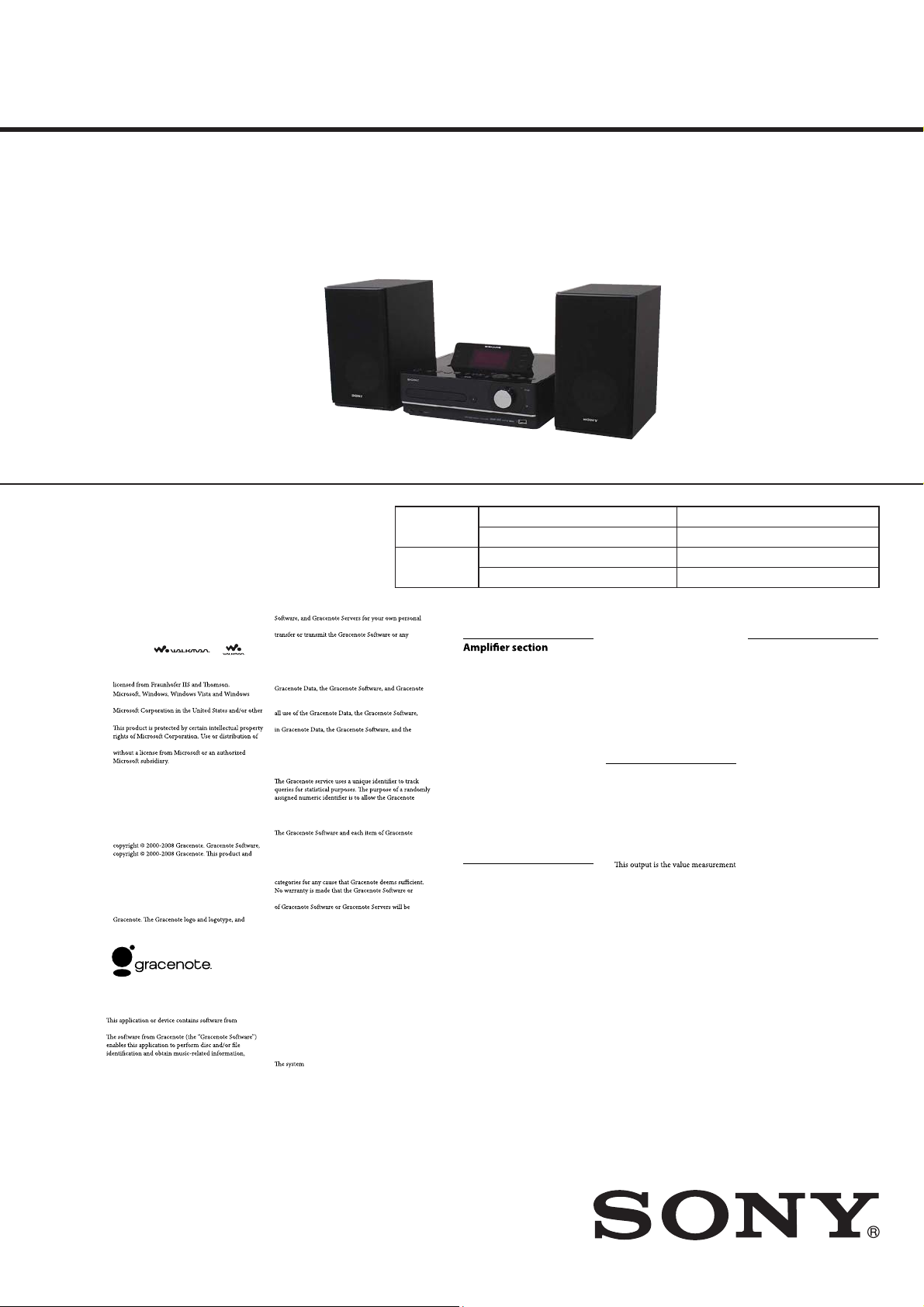
• SS-CE35HD is the speaker system of
NAS-E35HD.
CD Section
HD Section
Trademarks, etc.
“GIGA JUKE” andits logo are trademarks of Sony
•
Corporation.
Title Updater is a trademarkof S onyCorporation.
•
“WALKMAN”,
•
registered trademarks of Sony Corporation.
MICROVAULTis a trademark of Sony Corporation.
•
MPEG Layer-3 audio coding technology and patents
•
•
Media are trademarks or registered trademarks of
countries.
•
such technology outside of this product is prohibited
BuiltwithLinterDatabase.
•
Copyright © 2006-2007, Brycen Corp., Ltd.
Copyright © 1990-2003, Relex, Inc., All rights reserved.
Music recognition technology and relateddata are
•
provided by Gracenote®. Gracenoteis the industr y
standard in music recognition technology and related
content delivery.For more information, please visit
www.gracenote.com.
CD and music-related dataf romGracenote, Inc.,
service may practice one or more of the followingU.S.
Patents: #5,987,525; #6,061,680; #6,154,773, #6,161,132,
#6,230,192, #6,230,207, #6,240,459, #6,330,593, and
other patents issued or pending. Some services supplied
under license from Open Globe, Inc. for U.S.Patent:
#6,304,523.
Gracenote and CDDB are registered trademarks of
the “Poweredby Gracenote” logo are trademarks of
Gracenote.
Gracenote® End User License
Agreement
Gracenote, Inc. of Emeryville, California (“Gracenote”).
including name, artist, track, and title information
(“Gracenote Data”)from online servers or embedded
databases (collectively,“Gracenote Servers”) and to
perform other functions. Youmay use Gracenote Data
only by means of the intended End-Userfunctions of this
application or device.
and are
Youagree that you will use Gracenote Data, the Gracenote
non-commercial use only.You agree not to assign, copy,
Gracenote Data to any third party.YOU AGREE NOT
TO USE OR EXPLOIT GRACENOTEDATA, THE
GRACENOTE SOFTWARE, OR GRACENOTE SERVERS,
EXCEPT AS EXPRESSLYPERMITTED HEREIN.
Youagree that your non-exclusive license to use the
Servers will terminate if you violate these restrictions.
If your license terminates, you agreeto ceas e anyand
and Gracenote Servers. Gracenote reserves all rights
Gracenote Servers, including all ownership rights. Under
no circumstances will Gracenote become liable for any
payment to you for any informati on that you provide. You
agree that Gracenote, Inc. may enforceits rights under this
Agreement against you directly in its ownname.
service to count queries without knowing anythingabout
who you are. For more information,se e the web page for
the Gracenote Privacy Policy for the Gracenote service.
Data are licensed to you “AS IS.”Gracenote makes
no representationsor warranties, express or implied,
regarding the accuracy of any Gracenote Data from in
the Gracenote Servers. Gracenote reserves the right to
delete data from the Gracenote Servers or to change data
Gracenote Servers are error-free or that functioning
uninterrupted. Gracenote is notobligated to provide you
with new enhanced or additional datatyp esor categories
that Gracenote may provide in thefuture and is free to
discontinue its services at any time.
GRACENOTE DISCLAIMS ALL WARRANTIES
EXPRESS OR IMPLIED, INCLUDING,BUT
NOT LIMITED TO, IMPLIED WARRANTIES OF
MERCHANTABILITY, FITNESS FOR A PARTICULAR
PURPOSE, TITLE, AND NON-INFRINGEMENT.
GRACENOTE DOES NOT WARRANT THE RESULTS
THAT WILL BEOBTAINED BY YOUR USE OF THE
GRACENOTE SOFTWAREOR ANY GRACENOTE
SERVER. IN NO CASE WILL GRACENOTEBE LIABLE
FOR ANY CONSEQUENTIAL OR INCIDENTAL
DAMAGES OR FOR ANY LOSTPROFITS OR LOST
REVENUES.
names and product names indicated in
this manual are generally the trademarks or registered
trademarks of the manufacturer.
™ and ® marks are omitted in thismanual.
European model:
DIN power output (rated):
24 + 24 W (8 Ω at 1 kHz, DIN)
Continuous RMS power output
(reference):
30 + 30 W (8 Ω at 1 kHz, 10 % THD)
Music Power output (reference):
30 + 30 W (8 Ω at 1 kHz, 10 % THD)
Other models:
DIN power output (rated):
24 + 24 W (8 Ω at 1 kHz, DIN)
Continuous RMS power output
(reference):
30 + 30 W (8 Ω at 1 kHz, 10 % THD)
HDD Jukebox section
Capacity:
80 GB*
* A portion of the memory is used
for system management functions.
Actual available memory is approx.
72 GB.
AEP Model
UK Model
E Model
Australian Model
Chinese Model
Model Name Using Similar Drive NEW
Optical Pick-up Block Name KSM215DHAP
Model Name Using Similar Drive NEW
Hard Disc Drive Name HDD/SG-NIGHTHAWK-S (80GB)
SPECIFICATIONS
Recording system:
MP3
Maximum recording time (measured
with MP3 128 kbps):
About 1,300 h
Maximum number of tracks:
20,000
Maximum number of albums:
2,000
CD player section
System:
Compact disc and digital audio
system
Laser Diode Properties:
Emission duration: continuous
Laser Output*: Less than 44.6 μw
*
at a distance of 200 mm from the
objective lens surface on the Optical
Pick-up Block with 7 mm aperture.
Frequency response:
20 Hz - 20 kHz
USB section
Supported bit rate
MP3 (MPEG-1 Audio Layer3):
32 - 320 kbps, VBR
WMA:
48 - 192 kbps, VBR
AAC:
48 - 320 kbps
Sampling frequencies
MP3 (MPEG-1 Audio Layer3):
32/44.1/48 kHz
WMA:
44.1 kHz
AAC:
44.1 kHz
– Continued on next page –
NAS-E35HD
HDD AUDIO SYSTEM
SS-CE35HD
9-889-128-02
2008F05-1
2008.06
©
SPEAKER SYSTEM
Sony Corporation
Audio Business Group
Published by Sony Techno Create Corporation
Page 2
NAS-E35HD/SS-CE35HD
Ver. 1.1
FM tuner section
Tuner:
FM stereo, FM superheterodyne
tuner
Circuit system:
PLL digital frequency synthesizer
quarts lock system
Frequency range:
Brazilian model:
87.5 - 108.0 MHz (100kHz step)
Other models:
87.5 - 108.0 MHz (50kHz step)
Antenna:
FM lead antenna
Antenna terminals:
75 Ω unbalanced
Intermediate frequency:
10.7 MHz
AM tuner section
Tuner:
AM superheterodyne tuner
Circuit system:
PLL digital frequency synthesizer
quarts lock system
Frequency range:
European model:
531 - 1,602 kHz (with the
interval set at 9 kHz)
LatinAmericanmodel:
530 - 1,710 kHz (with the
interval set at 10 kHz)
531 - 1,710 kHz (with the
interval set at 9 kHz)
Oceanian model
531 - 1,710 kHz (with the
interval set at 9 kHz)
530 - 1,710 kHz (with the
interval set at 10 kHz)
Other models:
531 - 1,602 kHz (with the
interval set at 9 kHz)
530 - 1,610 kHz (with the
interval set at 10 kHz)
Antenna:
AM loop antenna
Antenna terminals:
External antenna terminal
Intermediate frequency:
450 kHz
DAB tuner section (UK
model only)
Tuner:
DABstereotuner
Antenna:
DAB lead antenna
Frequency range:
Band-III: 174.928 (5A) – 239.200
(13F) MHz
DAB frequency table (Band-III):
Frequency Label
174.928 MHz 5A
176.640 MHz 5B
178.352 MHz 5C
180.064 MHz 5D
181.936 MHz 6A
183.648 MHz 6B
185.360 MHz 6C
187.072 MHz 6D
188.928 MHz 7A
190.640 MHz 7B
192.352 MHz 7C
194.064 MHz 7D
195.936 MHz 8A
197.648 MHz 8B
199.360 MHz 8C
201.072 MHz 8D
202.928 MHz 9A
204.640 MHz 9B
206.352 MHz 9C
208.064 MHz 9D
209.936 MHz 10A
211.648 MHz 10B
213.360 MHz 10C
215.072 MHz 10D
216.928 MHz 11A
218.640 MHz 11B
220.352 MHz 11C
222.064 MHz 11D
223.936 MHz 12A
225.648 MHz 12B
227.360 MHz 12C
229.072 MHz 12D
230.784 MHz 13A
232.496 MHz 13B
234.208 MHz 13C
235.776 MHz 13D
237.488 MHz 13E
239.200 MHz 13F
Inputs/Outputs
AUDIO IN (stereo mini jack):
Voltage 0.8 V, impedance 22 k
(USB) port:
USB type A, Full speed USB
DMPORT:
For conne cting a DIGI TA L MEDIA
PORT adapter
(headphones) jack (stereo mini jack):
Accepts headphones of 8 Ω or
more
Asian model:
AUDIO OUT (phono jacks):
Voltage 0.5 V, impedance 1 k
Speaker
(SS-CE35HD)
Latin American model:
Speaker system:
Speaker units:
Woofer: 120 mm, cone type
Nominal impedance:
8 Ω
Dimensions (w/h/d)
Approx. 140 × 284 × 240 mm
Mass
Approx. 2.7 kg net per speaker
Other models:
Speaker system:
Speaker units:
Woofer: 120 mm, cone type
Tweeter: 40 mm, cone type
Nominal impedance:
8 Ω
Dimensions (w/h/d)
Approx. 140 × 250 × 210 mm
Mass
Approx. 2.0 kg net per speaker
General
Power requirements:
Mexican model:
120 V AC, 60 Hz
Taiwan mod el:
120 V AC, 50/60 Hz
Brazilian mod el:
127 or 220 V AC, 50/60 Hz
(adjustable with voltage selector)
Latin American model (except
for the Mexican, Argentine and Brazilian models):
110 - 120 or 220 - 240 V AC,
50/60 Hz (adjustable with voltage
selector)
Other models:
220 - 240 V AC, 50/60 Hz
Power consumption:
45 W
Dimensions (w/h/d):
UK model:
Approx. 285 × 130 × 319 mm
incl. projecting parts and
controls
Other models:
Approx. 285 × 130 × 312 mm
incl. projecting parts and
controls
Mass:
Approx. 4.0 kg
Operating temperature:
+5
°C (+41 °F) to +35 °C (+95 °−F)
Operating humidity:
25 % to 80 %
Supplied accessories:
AM loop antenna (1)
FM lead antenna (1)
DAB lead antenna (1)
(for the UK model only)
Speaker cords (2)
Speaker pads (8)
(for the Latin American model only)
Remote control (1)
R6 (size AA) batteries (2)
DIGITAL MEDIA PORT adapter
(TDM-iP10 (M) ) (1)
(for the European model only)
iPod Dock Adapters (1 set)
(for the European model only)
Operating Instructions
subjecttochangewithoutnotice.
NOTES ON CHIP COMPONENT REPLACEMENT
• Never reuse a disconnected chip component.
• Notice that the minus side of a tantalum capacitor may be damaged by heat.
FLEXIBLE CIRCUIT BOARD REPAIRING
• Keep the temperature of soldering iron around 270 °C during
repairing.
• Do not touch the soldering iron on the same conductor of the
circuit board (within 3 times).
• Be careful not to apply force on the conductor when soldering
or unsoldering.
CAUTION
Use of controls or adjustments or performance of procedures
other than those specifi ed herein may result in hazardous radia-
tion exposure.
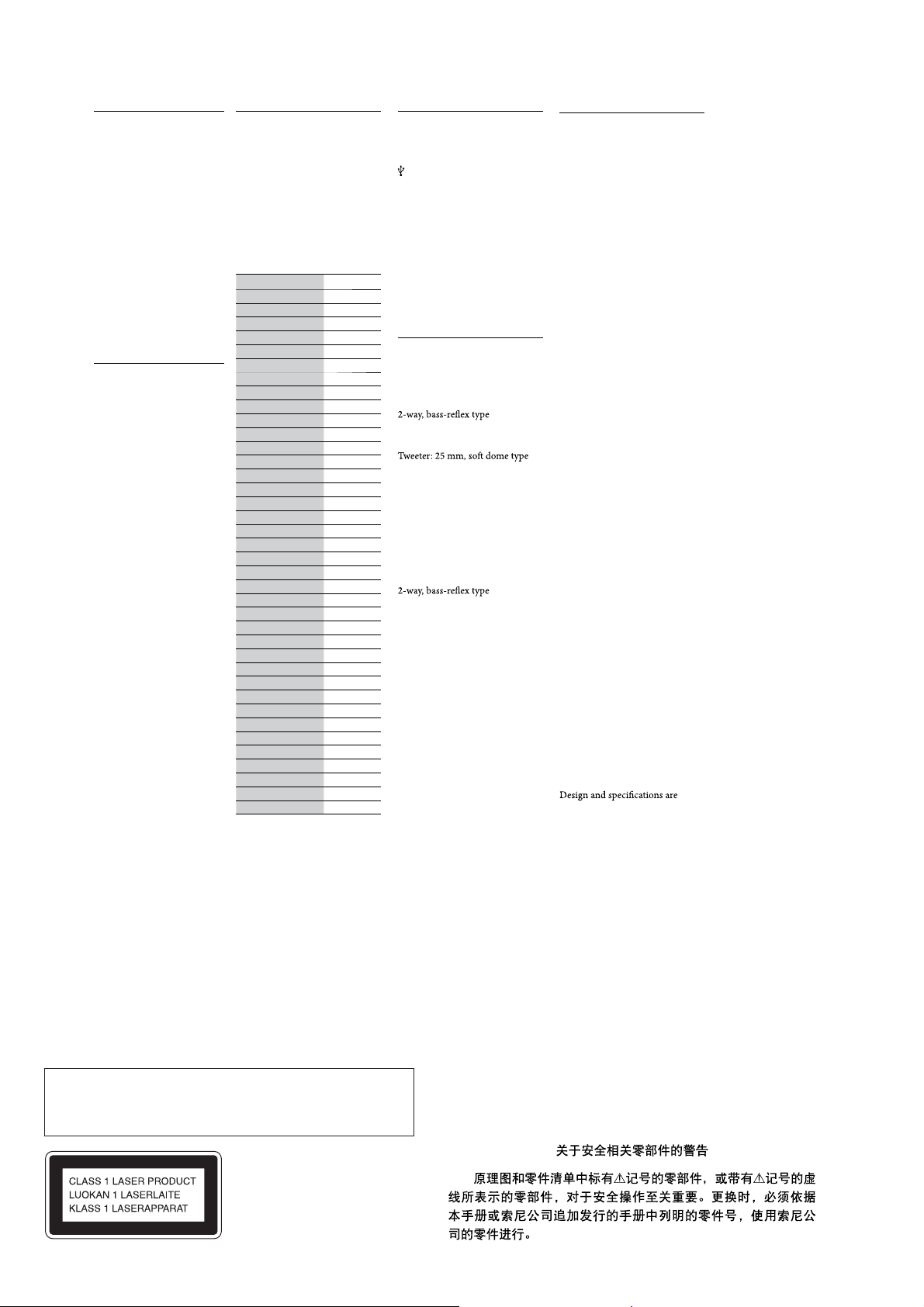
This appliance is classifi ed as
a CLASS 1 LASER product.
This marking is located on the
rear or bottom exterior.
2
SAFETY-RELATED COMPONET WARNING!
COMPONENTS IDENTIFIED BY MARK 0 OR DOTTED LINE
WITH MARK 0 ON THE SCHEMATIC DIAGRAMS AND IN
THE PARTS LIST ARE CRITICAL TO SAFE OPERATION.
REPLACE THESE COMPONENTS WITH SONY PARTS
WHOSE PART NUMBERS APPEAR AS SHOWN IN THIS
MANUAL OR IN SUPPLEMENTS PUBLISHED BY SONY.
Page 3

TABLE OF CONTENTS
NAS-E35HD/SS-CE35HD
1. SERVICING NOTES ............................................. 4
2. GENERAL .................................................................. 6
3. DISASSEMBLY
3-1. Disassembly Flow ........................................................... 8
3-2. Panel (Side L/R) .............................................................. 9
3-3. Top Panel Block .............................................................. 9
3-4. HP JACK Board, KEY (FRONT) Board,
Panel (Front) Assy .......................................................... 10
3-5. POWER Board ................................................................ 10
3-6. FL Block ......................................................................... 11
3-7. DISPLAY Board ............................................................. 11
3-8. DAB Board, DMP Board, Tuner (FM/AM) .................... 12
3-9. MAIN Board ................................................................... 13
3-10. CD Mechanism Block ..................................................... 13
3-11. USB MICOM Board ....................................................... 14
3-12. HDD Assy ....................................................................... 14
3-13. Base Unit ......................................................................... 15
3-14. Belt .................................................................................. 15
3-15. OP Base Assy (KSM215DHAP) ..................................... 16
4. TEST MODE ............................................................ 17
5. ELECTRICAL CHECKS ...................................... 20
6. DIAGRAMS
6-1. Block Diagram - CD SERVO, PANEL Section -............ 21
6-2. Block Diagram - USB, HDD Section - ........................... 22
6-3. Block Diagram - MAIN Section - ................................... 23
6-4. Block Diagram - POWER SUPPLY Section - ................ 24
6-5. Printed Wiring Board - CD Board - ................................ 26
6-6. Schematic Diagram - CD Board - ................................... 27
6-7. Schematic Diagram - USB MICOM Board (1/4) - ......... 28
6-8. Schematic Diagram - USB MICOM Board (2/4) - ......... 29
6-9. Schematic Diagram - USB MICOM Board (3/4) - ......... 30
6-10. Schematic Diagram - USB MICOM Board (4/4) - ......... 31
6-11. Printed Wiring Board - USB MICOM Board - ............... 32
6-12. Schematic Diagram - MAIN Board (1/3) - ..................... 33
6-13. Schematic Diagram - MAIN Board (2/3) - ..................... 34
6-14. Schematic Diagram - MAIN Board (3/3) - ..................... 35
6-15. Printed Wiring Board
- MAIN Board (Component Side) - ................................ 36
6-16. Printed Wiring Board
- MAIN Board (Conductor Side) - .................................. 37
6-17. Printed Wiring Boards - DAB, DMP Section - ............... 38
6-18. Schematic Diagram - DAB, DMP Section - ................... 39
6-19. Printed Wiring Board - D-AMP Board - ......................... 40
6-20. Schematic Diagram - D-AMP Board - ............................ 41
6-21. Printed Wiring Boards - SPEAKER Section - ................ 42
6-22. Schematic Diagram - SPEAKER Section - .................... 42
6-23. Printed Wiring Board
- DISPLAY Board (Component Side) - .......................... 44
6-24. Printed Wiring Board
- DISPLAY Board (Conductor Side) - ............................ 45
6-25. Schematic Diagram - DISPLAY Board (1/2) - ............... 46
6-26. Schematic Diagram - DISPLAY Board (2/2) - ............... 47
6-27. Printed Wiring Boards - PANEL Section - ..................... 48
6-28. Schematic Diagram - PANEL Section - .......................... 49
6-29. Printed Wiring Board - D/D CON Board - ..................... 50
6-30. Schematic Diagram - D/D CON Board - ........................ 51
6-31. Printed Wiring Board - POWER Board - ........................ 52
6-32. Schematic Diagram - POWER Board - .......................... 53
6-33. Printed Wiring Board - MOTOR Board - ....................... 54
6-34. Schematic Diagram - MOTOR Board - .......................... 54
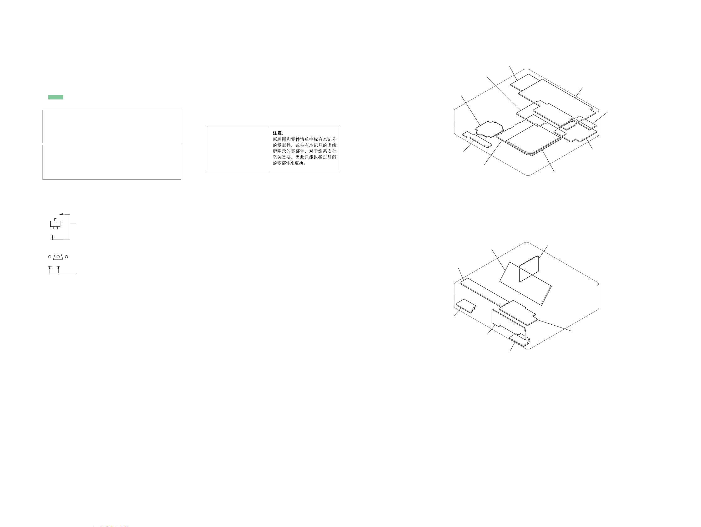
7. EXPLODED VIEWS
7-1. Panel Section ................................................................... 73
7-2. Top Panel Section ........................................................... 74
7-3. Main Section ................................................................... 75
7-4. HDD Section ................................................................... 76
7-5. Chassis Section ............................................................... 77
7-6. Loading Mechanism Section .......................................... 78
7-7. Base Unit Section ............................................................ 79
7-8. Speaker Section (SS-CE35HD) ...................................... 80
8. ELECTRICAL PARTS LIST .............................. 81
Accessories are given in the last of the electrical parts list.
3
Page 4
NAS-E35HD/SS-CE35HD
Ver. 1.1
SECTION 1
SERVICING NOTES
NOTES ON HANDLING THE OPTICAL PICK-UP
BLOCK OR BASE UNIT
The laser diode in the optical pick-up block may suffer electrostatic break-down because of the potential difference generated by the
charged electrostatic load, etc. on clothing and the human body.
During repair, pay attention to electrostatic break-down and also
use the procedure in the printed matter which is included in the
repair parts.
The fl exible board is easily damaged and should be handled with
care.
NOTES ON LASER DIODE EMISSION CHECK
The laser beam on this model is concentrated so as to be focused
on the disc refl ective surface by the objective lens in the optical
pickup block. Therefore, when checking the laser diode emission,
observe from more than 30 cm away from the objective lens.
UNLEADED SOLDER
Boards requiring use of unleaded solder are printed with the leadfree mark (LF) indicating the solder contains no lead.
(Caution: Some printed circuit boards may not come printed with
the lead free mark due to their particular size)
: LEAD FREE MARK
Unleaded solder has the following characteristics.
• Unleaded solder melts at a temperature about 40 °C higher
than ordinary solder.
Ordinary soldering irons can be used but the iron tip has to be
applied to the solder joint for a slightly longer time.
Soldering irons using a temperature regulator should be set to
about 350 °C.
Caution: The printed pattern (copper foil) may peel away if
the heated tip is applied for too long, so be careful!
• Strong viscosity
Unleaded solder is more viscous (sticky, less prone to fl ow)
than ordinary solder so use caution not to let solder bridges
occur such as on IC pins, etc.
• Usable with ordinary solder
It is best to use only unleaded solder but unleaded solder may
also be added to ordinary solder.
RELEASING THE DISC TRAY LOCK
The disc tray lock function for the antitheft of an demonstration
disc in the store is equipped.
Releasing Procedure:
1. Press [
] button to turn the power on.
?/1
2. Press the [FUNCTION] button to select CD function.
3. While pressing the [
] button, press the [Z] button for more 5
x
seconds).
4. The message “UNLOCKED” is displayed and the disc tray is
unlocked.
Note: When “LOCKED” is displayed, the slot lock is not released by
turning power on/off with the [
?/1
] button.
NOTE THE IC1, IC5 AND IC13 ON THE USB MICOM
BOARD REPLACING
IC1, IC5 and IC13 on the USB MICOM board cannot exchange
with single. When IC1, IC5 and IC13 on the USB MICOM board
are damaged, exchange the entire mounted board.
MODEL IDENTIFICATION
– Rear View –
POWER VOLTAGE
INDICATION
Model Power Voltage Indication
Mexican model 120V - 60Hz 45W
Taiwan model 120V - 50/60Hz 45W
Brazilian model 127/220V - 50/60Hz 45W
Chilean and Peruvian models
AEP, Russian, UK, Hong Kong,
Argentina, Korean, Thai, Australian and Chinese models
110-120/220-240V - 50/60Hz
45W
220-240V - 50/60Hz 45W
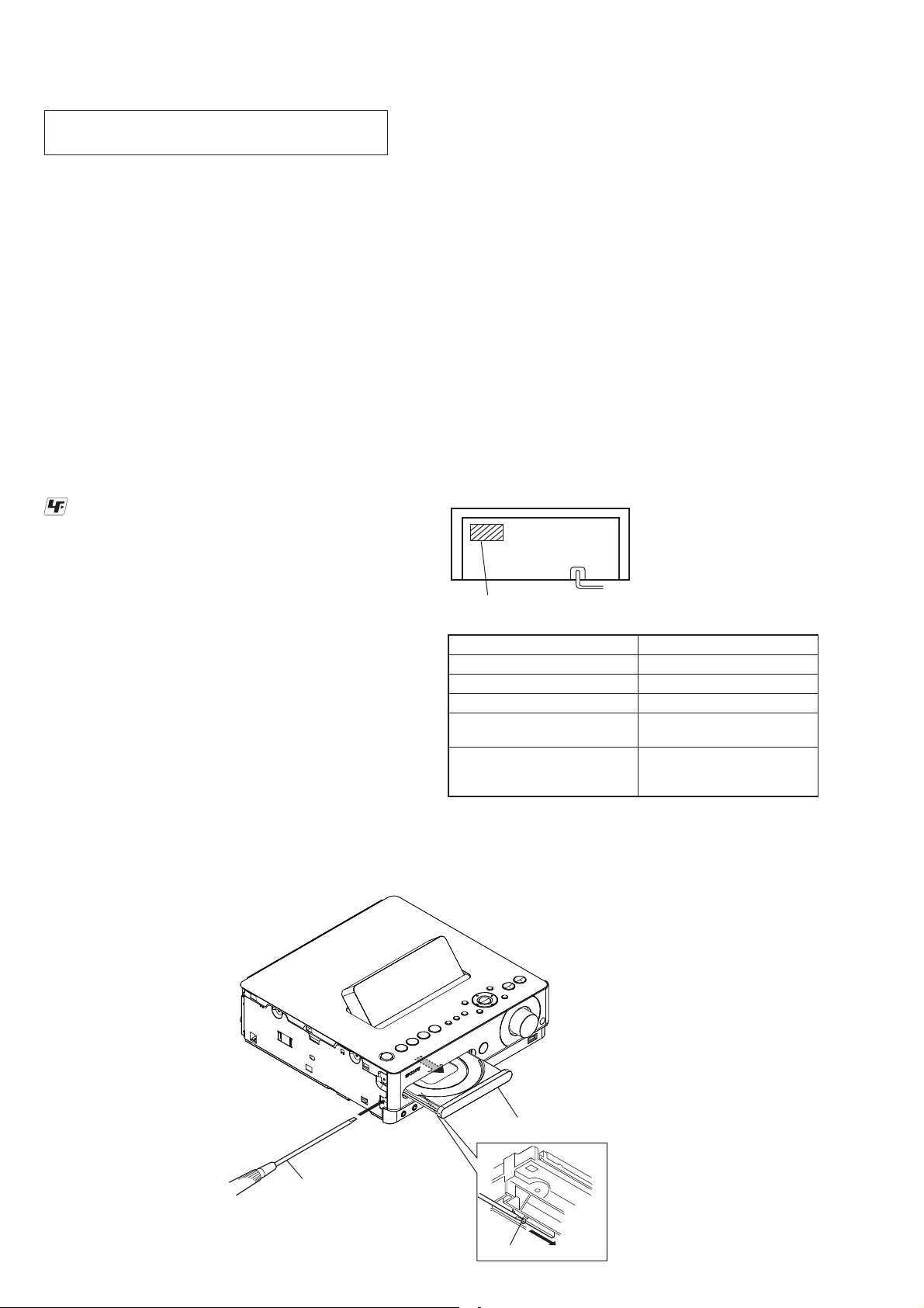
HOW TO OPEN THE TRAY WHEN POWER SWITCH TURN OFF
Note: Please insert a screwdriver after removing the panel (side L).
About disassembly of the panel (side L), please refer to “3-2. Panel (Side L/R)” (page 13).
Insert the screw driver.
Push the boss.
4
Open the tray.
Page 5
NAS-E35HD/SS-CE35HD
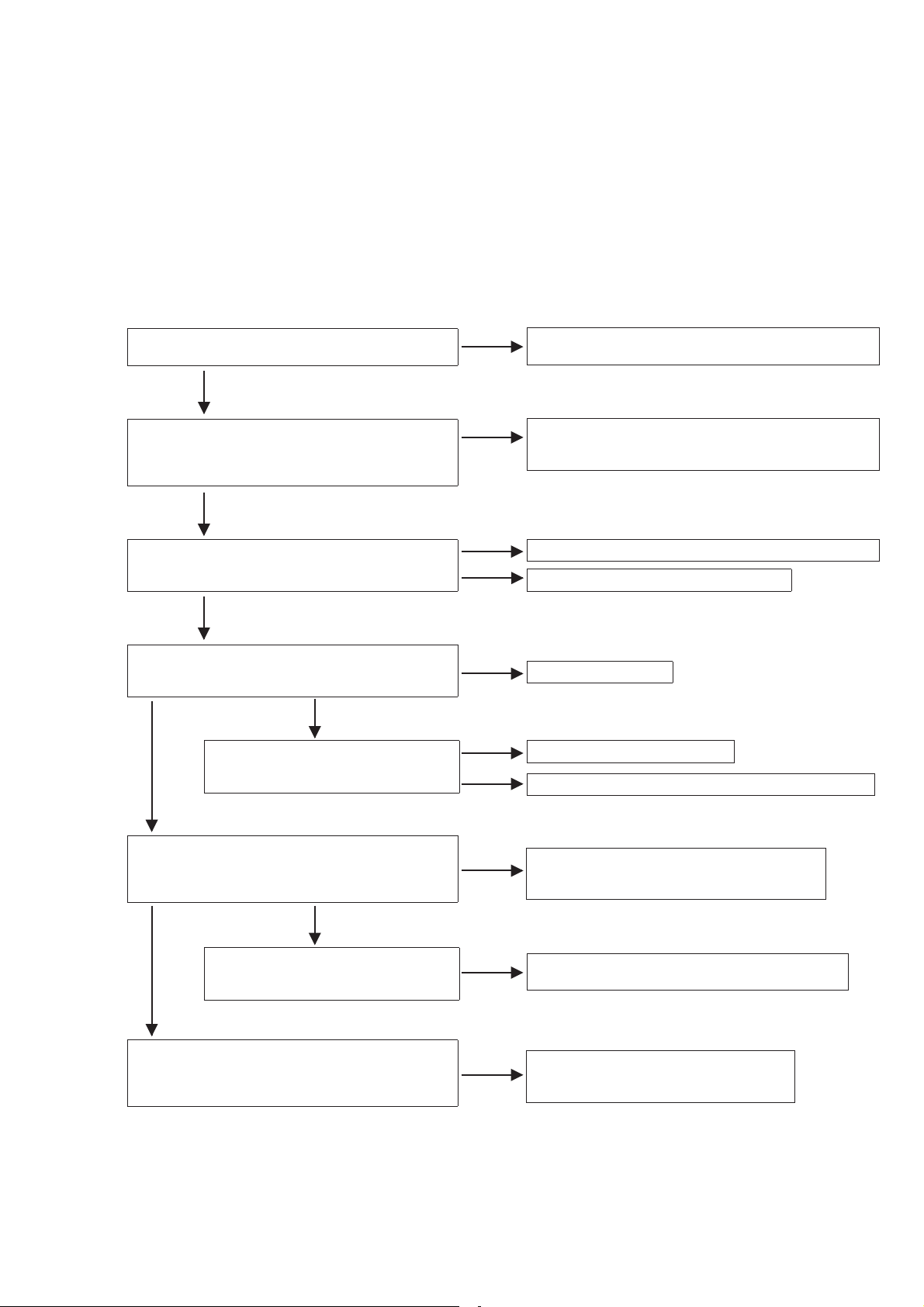
REPLACEMENT PROCEDURE OF HDD
1. Prior Notes
• It is backup in the customer in preparation for the HDD exchange as for the tune recorded to HDD beforehand.
• Note that all recorded tunes are deleted when “Factory Reset" is done.
2. Common Check
Procedure:
1. Execute “COLD RESET” (Refer to page 17) after confi rming the symptom.
2. Confi rm the installation of HDD.
3. Confi rm the power supply to HDD.
4. Confi rm the state to HDD of the connecting cable and the connector.
3. Procedure According To Symptom
Symptom 1 : HDD doesn't rotate.
The set symptom : HDD doesn't rotate.
Another symptom
Yes
Correspondence : If the power supply is normal, HDD is a
defective possibility size.
Ver. 1.1
Symptom 2 : The allophone does from HDD.
The set symptom : “HDD Reading” doesn't end, or the
HDD function doesn't operate normally.
Another symptom
Possible to reproduce
Symptom 3 : “HDD Reading” doesn't end.
The set symptom : Can CD reproduce?
Another symptom
Symptom 4 : HDD cannot reproduction/record-
ing/be forwarded.
Confi rmation 1 : Did “HDD Reading” end?
Not possible to reproduce
It ended
Another symptom
Confi rmation 2 : Can USB reproduce?
Possible to reproduce
Not possible to reproduce
Symptom 5 : “Data Error” is displayed by a spe-
Confi rmation 1 : Is it a tune where the copyright is
cifi c tune.
protected?
Yes
Correspondence : It judges compared with normal goods,
Both the HDD and USB MICOM board are defective doubts.
The USB MICOM board is a defective doubt.
It doesn't end
Reconfi rm symptom 2.
HDD is a defective possibility size.
Both the HDD and USB MICOM board are defective doubts.
Yes
It becomes this symptom if the tune where the copyright is protected is taken by way of USB, and it is
not possible to reproduce (product specifi cation).
and if it is an obviously abnormal sound,
HDD is a defective possibility size.
Another symptom
Confi rmation 2 : Is the extension of the
Symptom 6 : “Data Error” is always displayed.
Confi rmation 1 : Does this symptom occur even if
“COLD RESET” (Refer to page 17)
is executed?
No
fi le of the tune correct?
Yes
Yes
This display appears when the extension of the fi le is not
corresponding to the content (product specifi cation).
When this symptom occurs even if “Initialization Mode For Factory” (Refer to page 18) is
executed, HDD is a defective possibility size.
Execute “HDD Writing/Reading Test” (Refer to page 18) 3 times when these symptoms do not reproduce it. It can be judged that HDD
is normal if NG is not generated.
4. Processing After HDD Is Replaced
Procedure:
1. Confi rm the execution of “HDD Writing/Reading Test” (Refer to page 18), and not becoming NG.
2. Execute “CDDB Version Display” (Refer to page 18), and confi rm the CDDB version is 989 (South American model) or 988(Except
South American model).
3. Confi rm the tune can be recorded from CD to HDD, and the tune be reproduced normally.
4. Execute “Initialization Mode For Factory” (Refer to page 18) at the end.
5
Page 6
NAS-E35HD/SS-CE35HD
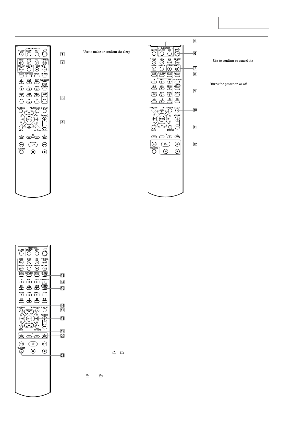
Remote control
SLEEP button
setting.
Playback buttons
Use to select the function directly and
start playback at the same time.
HDD button
•
USB button
•
CD button
•
TUNER/BAND button
•
DMPORT button
•
AUDIO IN button
•
DSGX and EQ buttons
DSGX button
•
Use to generate a more dynamic sound
(Dynamic Sound Generator X-tra).
Each press of the button switches the
DSGX function “ON” or “OFF”. is
function is factory set to “ON”.
EQ (equalizer) button
•
Use to adjust the bass and treble.
Press this button to display “BASS”,
andthenpressor to adjust
the bass. Aer adjusting the bass
sound, press this button again to
display “TREBLE”, and then press
or to adjust the treble.
VOLUME+* and VOLUME– buttons
Useto adjustthevolume.
An asterisk (*) indicates buttons that
have a tactile dot (the VOLUME +
button).
SECTION 2
GENERAL
timer
An asterisk (*) indicates buttons that
have a tactile dot (the number “5”
button and (play) button of the
operation buttons ).
This section is extracted
from instruction manual.
CLOCK/TIMER buttons
Usetosettheclockortimer.
SELECT button
•
setting.
SET button
•
Use to display the clock or timer menu.
/ (power) button
HDD REC buttons
Use for recording to the HDD Jukebox.
HDD REC (start recording) button
•
HDD REC (pause recording) button
•
PLAY MODE and REPEAT buttons
PLAY MODE button
•
Use to select a play mode.
REPEAT button
•
Use to select a repeat mode.
Numeric*/text buttons
Use to select a track during play or to
enter text.
Use to select a preset FM or AM station
or a DAB service.
DISPLAY button
Use to display information such as time
information, clock, demonstration, etc.
OPTIONS button
Displays the Option menu.
Menu items will vary according to the
selected function.
Operation buttons
Use in all functions to perform basic
operations.
(play) button*
•
(fast rewind) and
•
(fast forward) buttons
(pause) button
•
(stop) button
•
timer
FM MODE button
Usetoselectstereoormonauralwhile
listening to an FM broadcast.
TUNING MODE button
Use to select the tuning mode.
TUNER MEMORY button
Use to preset a radio station or DAB
service (UK model only).
FUNCTION button
Use to select a function.
TITLE UPDATE button
Useto displaytheTitleUpdatemenu.
Menu operation buttons
Use to select menu items and enter menu
settings.
•
•
BACK button
Usetogobacktotheprevious display.
+ • –, • and
•
•
•
TRANSFER button
Use to transfer tracks to a USB device.
andbuttons
,,
Use to select a menu item or to change
asetting.
ENTER button
Use to enter a setting.
+ • – buttons
+ and – buttons
Use to adjust the tuning frequency.
andbuttons
Cues the beginning of a track.
+ and – buttons
Use to select an album or a folder.
6
Page 7
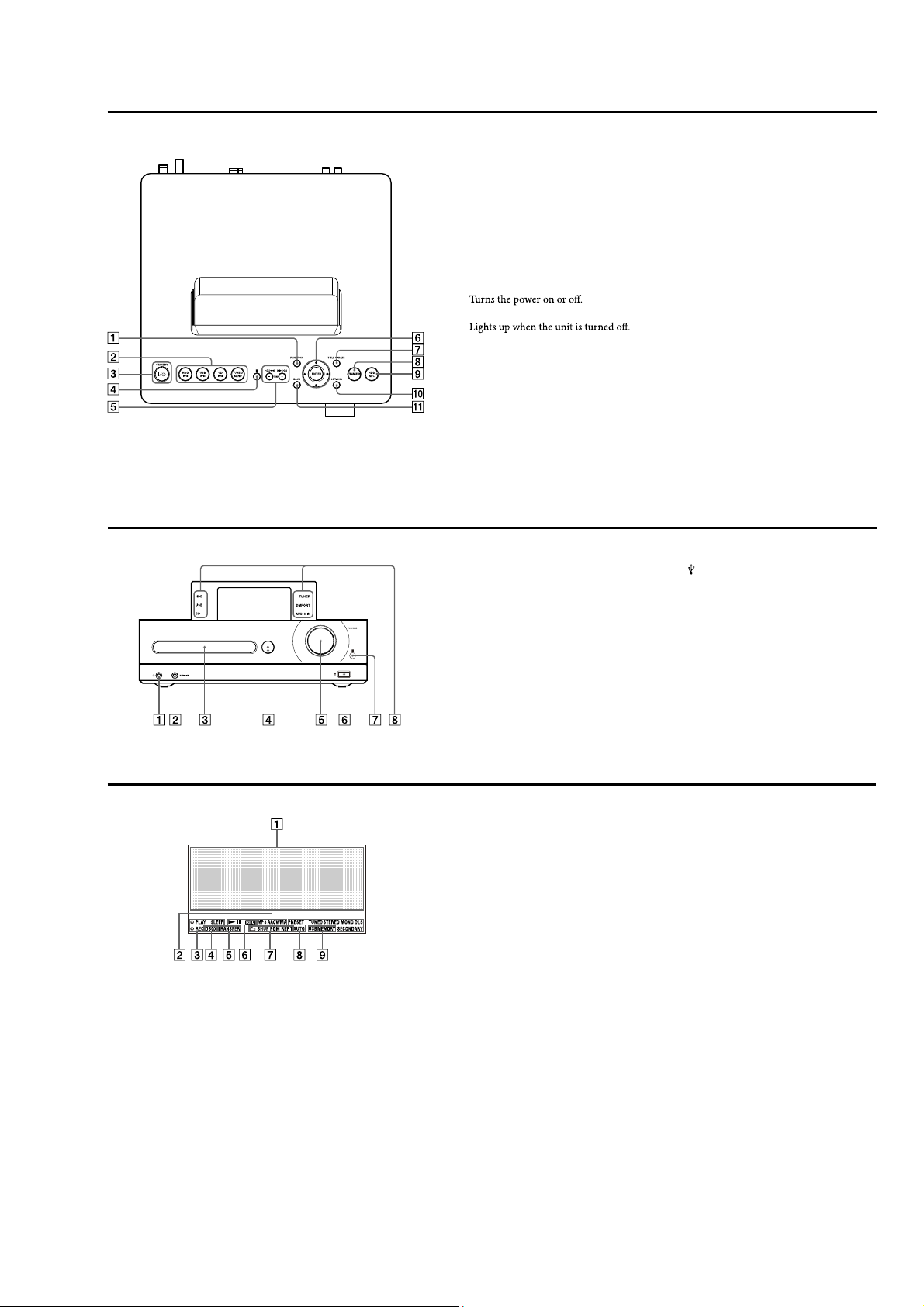
NAS-E35HD/SS-CE35HD
Top of the main unit
Front of the main unit
FUNCTION button
Use to select a function.
Playback buttons
Usetoselectthefunction directlyandstart
playback at the same time.
HDD button
•
USB button
•
CD button
•
TUNER/BAND button
•
/ (power) button and STANDBY
indicator
(power) button
•
STANDBY indicator
•
(stop) button
Use in each function to stop an operation.
• , • , and TUNE+ •
TUNE– buttons
andbuttons
•
Cues the beginning of a track.
andbuttons
•
Fast rewind and fast forward the playback.
TUNE + and TUNE – buttons
•
Use to adjust the tuning frequency.
(headphones) jack
Use to connect headphones.
AUDIO IN jack
Use to connect the audio output jack of an
external component.
Disc tray
Use to load a CD.
CD button
Opens and closes the disc tray.
Menu operation buttons
Use to select menu items and enter menu
settings.
•
•
TITLE UPDATE button
Useto displaytheTitleUpdatemenu.
For the UK model
TITLE UPDATE/DAB AUTO SCAN button
•
TRANSFER button
Use to transfer tracks to a USB device.
HDD REC button
Useforrecordingtothe HDDJukebox.
OPTIONS button
Displays the Option menu.
Menu items will vary according to the
selected function.
BACK button
Usetogobacktotheprevious display.
VOLUME dial
Use to adjust the volume.
(USB) port
Use to connect a USB device.
Remote sensor
Function indicators
Lights up to indicate the selected function.
andbuttons
,,
Use to select a menu item or to change a
setting.
ENTER button
Use to enter a setting.
DAB AUTO SCAN button
Use to scan DAB services automatically
while the unit is in the DAB function.
Display
Text information
Displays text information, such as a track
name, album name, etc.
Audio format indicators
Lights up to indicate the audio format.
Timer indicators
Lights up when the Play Timer, Recording
Timer, or Sleep Timer is set.
DSGX indicator
Lights up when the DSGX function is set to
“ON”.
TRANSFER indicator
Lights up while audio data is being
transferred.
Operation status indicators
Lights up to indicate the current operation
status (playing, recording, or paused).
Play mode indicators
Lights up to indicate the current play mode.
Tuner reception indicators
Lights up when the respective radio
function is active.
USB MEMORY indicator
Lights up when a USB device is connected.
7
Page 8
NAS-E35HD/SS-CE35HD
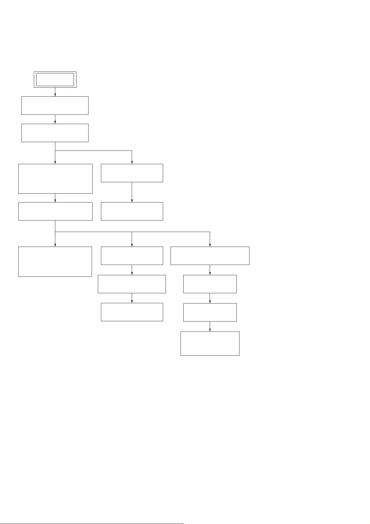
DISASSEMBLY
• This set can be disassembled in the order shown below.
3-1. DISASSEMBLY FLOW
SET
3-2. PANEL (SIDE L/R)
(Page 9)
3-3. TOP PANEL BLOCK
(Page 9)
SECTION 3
3-4. HP JACK BOARD,
KEY (FRONT) BOARD,
FRONT (PANEL) ASSY
(Page 10)
3-5. POWER BOARD
(Page 10)
3-8. DAB BOARD,
DMP BOARD,
TUNER (FM/AM)
(Page 12)
3-6. FL BLOCK
(Page 11)
3-7. DISPLAY BOARD
(Page 11)
3-9. MAIN BOARD
(Page 13)
3-11. USB MICOM BOARD
(Page 14)
3-12. HDD ASSY
(Page 14)
3-10. CD MECHANISM BLOCK
(Page 13)
3-13. BASE UNIT
(Page 15)
3-14. BELT
(Page 15)
3-15. OP BASE ASSY
(KSM215DHAP)
(Page 16)
8
Page 9
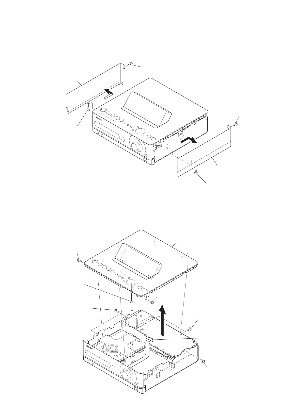
Note: Follow the disassembly procedure in the numerical order given.
3-2. PANEL (SIDE L/R)
panel (side L)
screw
(BVTP3 × 6)
screw
(BVTP3 × 8)
NAS-E35HD/SS-CE35HD
screw
(BVTP3 × 8)
3-3. TOP PANEL BLOCK
screw
(BVTP3 × 6)
connector
(CN401)
two screws
(BVTP3 × 6)
screw
(BVTP3 × 6)
top panel block
two screws
(BVTP3 × 6)
panel (side R)
screw
(BVTP3 × 6)
flexible flat cable (11 core)
(CNP402)
two screws
(BVTP3 × 6)
9
Page 10
NAS-E35HD/SS-CE35HD
Ver. 1.1
3-4. HP JACK BOARD, KEY (FRONT) BOARD, PANEL (FRONT) ASSY
flexible flat cable (5 core)
(CNP601)
connector
(CN303)
screw (B2.6)
R
screw (B2.6)
hold board
HP JACK board
screw
(BV3)
panel (front) assy
RL
two feet (felt)
RK
knob (volume)
3-5. POWER BOARD
three screws
(BV3)
coating clip
POWER board
RB
connector (CN909)
power cord connector
(CN01)
connector (CN901)
RI
sheet (RM)
RH
panel (front) assy
RL
RT
plate (key front PWB)
RE
three screws (B2.6)
RG
KEY (FRONT) board
two screws (B2.6)
RB
shield (key front PWB)
six screws
(BVTP3 × 6)
insulated plate
(power)
barrier (power B)
(AEP, RU, UK, E51,
MX, BR, AR)
10
flexible flat cable (5 core)
(CNP902)
barrier (power C)
(HK, TW, KR,
TH, AUS, CH)
• Abbreviation
AR : Argentina model
AUS : Australian model
BR : Brazilian model
CH : Chinese model
E51 : Chilean and Peruvian models
HK : Hong Kong model
KR : Korean model
MX : Mexican model
RU : Russian model
TH : Thai model
TW : Taiwan model
Page 11
3-6. FL BLOCK
Note: This illustration is seeing of top panel block from the inside.
flexible flat cable (9 core)
(CNP404)
two screws
(BVTP3 × 6)
FL block
NAS-E35HD/SS-CE35HD
screw
(BVTP3 × 6)
3-7. DISPLAY BOARD
case (FL) assy
filter (FL)
DISPLAY board
Remove solders.
flexible flat cable (9 core)
cover (FL)
two screws
(BVTP2.6)
11
Page 12
NAS-E35HD/SS-CE35HD
Ver. 1.1
3-8. DAB BOARD, DMP BOARD, TUNER (FM/AM)
screw
(BV3)
shield plate (tuner)
sheet (DMP) insulating
barrier (tuner)
two screws
(BV3)
bracket (DMP)
X
two screws
RL
(B2.6)
module
XT
(DAB tuner)
connector
RM
(CN602)
(UK)
Remove the solder.
coaxial connector
XB
(F type) (J601)
two screws
XE
(B2.6)
DMP board
RB
tuner (FM/AM)
RG
DAB board
XH
bracket
XG
(DAB)
two screws
(B2.6)
flexible flat cable (11 core) (CN813)
flexible flat cable (11 core) (CNP812)
flexible flat cable (9 core: Except AEP, UK
RT
models/11 core: AEP, UK models)
(tuner)
two screws (B2.6)
RE
two screws (B2.6)
two screws
RK
(B2.6)
nut
RI
(UK)
12
flexible flat cable (11 core)
RH
(CN601)
(UK)
Page 13
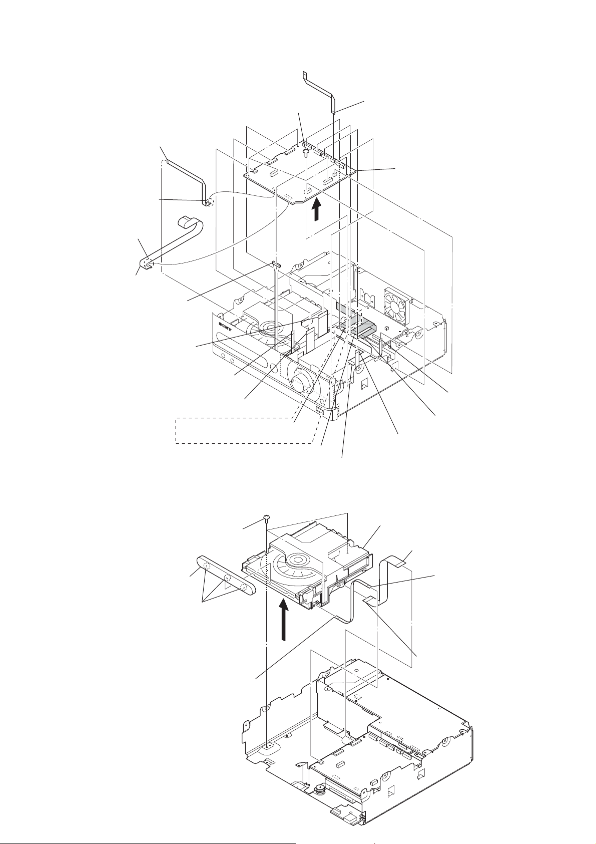
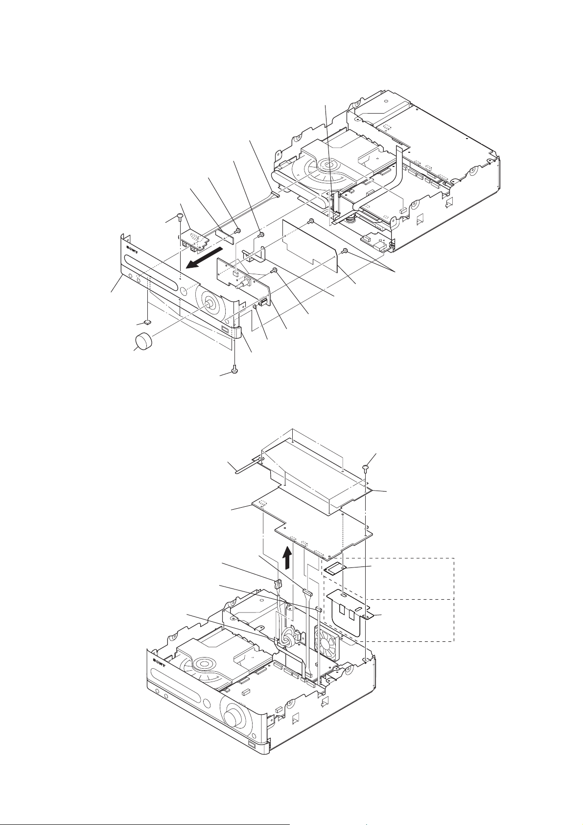
3-9. MAIN BOARD
flexible flat cable (5 core)
RT
(CNP601)
Remove the solder.
RK
Remove the solder.
RH
flexible flat cable
RI
(11 core)
connector (CN303)
four screws
RE
(BVTP3 × 6)
RG
NAS-E35HD/SS-CE35HD
flexible flat cable (5 core)
(CNP810)
MAIN board
RL
(with flexible flat cable (11 core/5core))
Ver. 1.1
flexible flat cable (19 core)
(CNP804)
flexible flat cable (5 core)
(CNP806)
flexible flat cable (17 core)
(CNP805)
(UK)
(CNP802)
3-10. CD MECHANISM BLOCK
three screws
(BV3)
ornamental plate (CD tray)
three claws
flexible flat cable (11 core)
flexible flat cable (11 core)
(CNP807)
flexible flat cable
(11 core) (CNP801: AEP, UK models)/
(9 core) (CNP808: Except AEP, UK models)
flexible flat cable (7 core)
RB
(CNP301)
CD mechanism block
flexible flat cable (19 core)
(MAIN board: CNP804)
flexible flat cable (5 core)
(CNP302)
flexible flat cable (11 core)
(CNP803)
flexible flat cable (5 core)
(MAIN board: CNP806)
flexible flat cable (5 core)
(MOTOR board: CN001)
flexible flat cable (19 core)
(CD board: CN101)
13
Page 14
NAS-E35HD/SS-CE35HD
Ver. 1.1
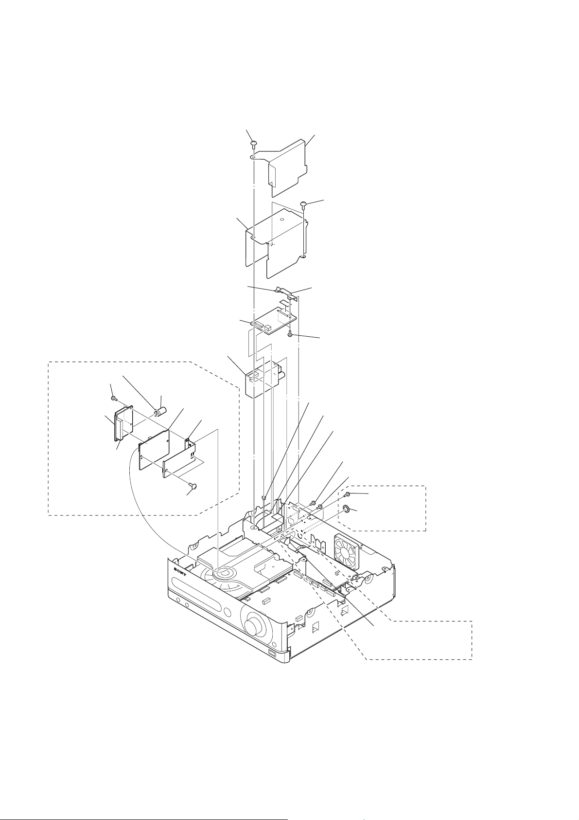
3-11. USB MICOM BOARD
flexible flat cable (5 core)
(CN2)
flexible flat cable (17 core)
(CN3)
four screws
RB
(BVTP3 × 6)
screw (B2.6)
barrier (power B)
sheet (USB micro computer)
shield plate (USB MICOM PWB)
four screws
(BVTP3 × 6)
USB MICOM board
RE
chassis (USB MICOM PWB)
RT
connector (CN7)
(Taiwan model)
connector (CN8)
R
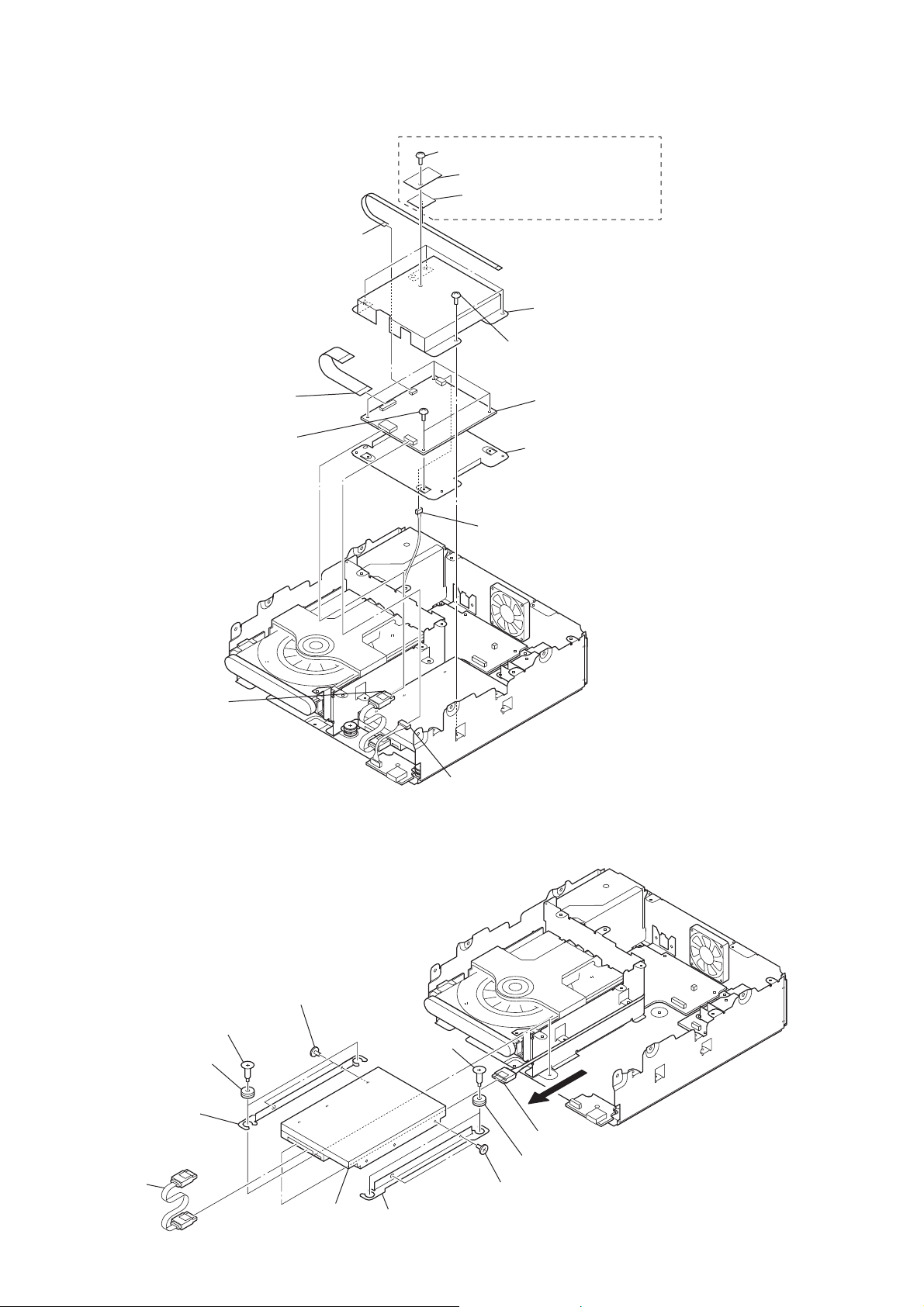
3-12. HDD ASSY
two HDD damper screws
two dampers
bracket (HDD R)
harness
two screws
(6-32UNCX5)
HDD assy
two HDD
damper screws
bracket (HDD L)
connector (CN6)
two screws
(6-32UNCX5)
harness
two dampers
14
Page 15
3-13. BASE UNIT
two floating screws
two springs (insulator)
floating screw
insulator
NAS-E35HD/SS-CE35HD
two floating screws
two springs
(insulator)
insulator
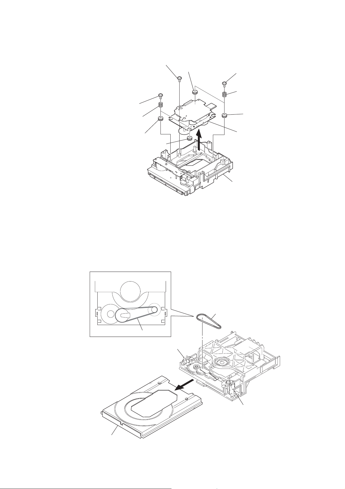
3-14. BELT
position of belt
insulator
insulator
– Bottom view –
base unit
loading (BK) assy
tray (AU)
belt
belt
claw
claw
15
Page 16
NAS-E35HD/SS-CE35HD
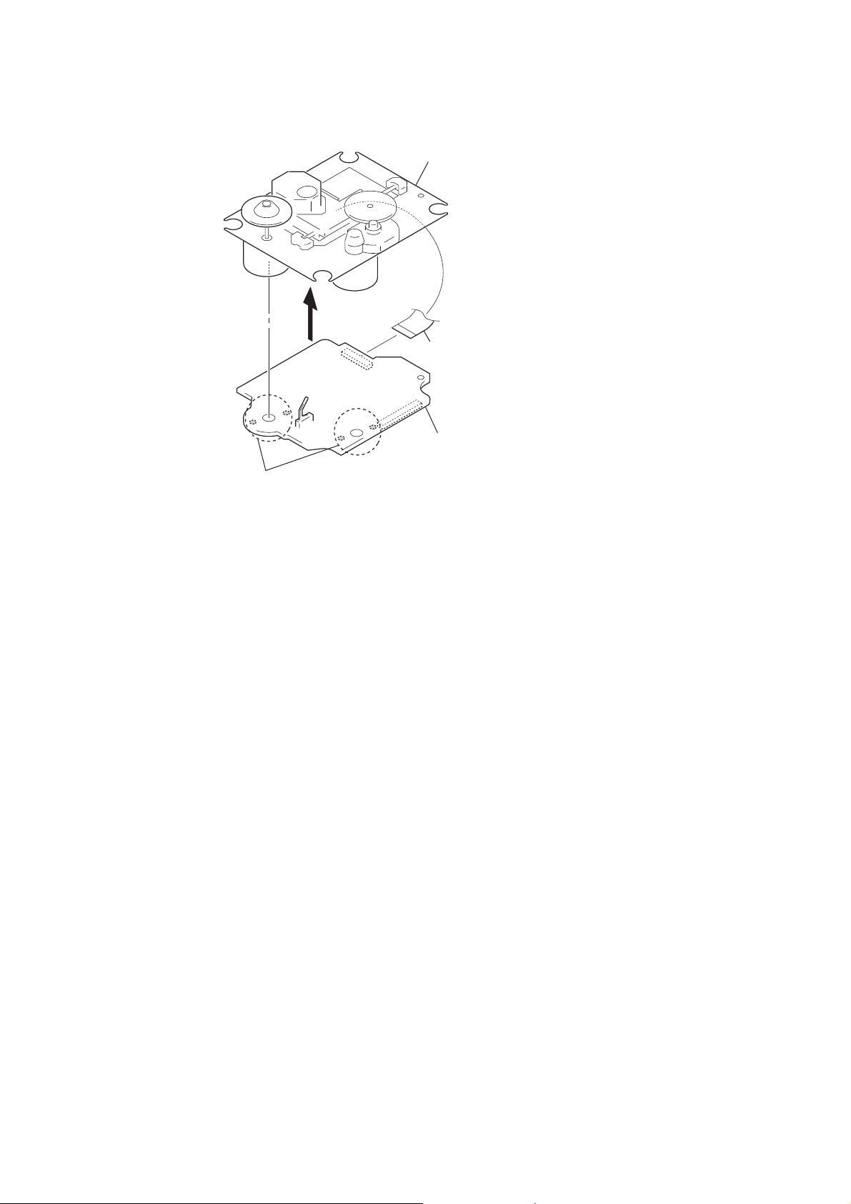
3-15. OP BASE ASSY (KSM215DHAP)
op base assy
(KSM215DHAP)
flexible flat cable (16 core)
(CN301)
CD board
Remove four solders.
16
Page 17

SECTION 4
TEST MODE
NAS-E35HD/SS-CE35HD
Ver. 1.1
Note: Never execute the item because the set might not operate
normally when the item being written, “Not used for the
servicing.” in each item is executed.
COLD RESET
The cold reset clears all data including preset data stored in the
memory to initial conditions. Execute this mode when returning
the set to the customer.
Procedure:
1. In the standby status, press the [
on.
2. Press three buttons of [
neously.
3. The set enters standby status.
], [ENTER] and at last [
x
] button to turn the power
?/1
] simulta-
?/1
PANEL TEST MODE
Enter The Panel Test Mode
Procedure:
1. In the standby status, press the [
on.
2. Press three buttons of [BACK], [x], and [Z] simultaneously.
3. When the panel test mode is activated, LEDs and segments of
the fulorescent indicator tube are all turned on.
Version Check
Procedure:
1. In the panel test mode (all LEDs and segments of the fulorescent indicator tube are turned on), press the [BACK] button.
2. On the fulorescent indicator tube, model name, destination,
MC version and its last updated date are displayed.
3. Each time [BACK] button is pressed, the display changes starting from MC, GC, GENE, GNS, HDD, USB, CD, CDMA,
CDMB, ST, T A, TM and CLA version this order, and returns to
the MC version display.
4. To release from this mode, press three buttons of [BACK],
[x], and [Z] simultaneously.
Key Test Mode
Procedure:
1. In the panel test mode (all LEDs and segments of the fulorescent indicator tube are turned on), press the [ENTER] button.
2. The message “KEY0 VOL0” displayed. Whenever any buttons are pressed and the [VOLUME] dial is turned, the value is
changed.
3. To release from this mode, press three buttons of [BACK],
[x], and [Z] simultaneously.
] button to turn the power
?/1
CD TRAY LOCK
This mode is for the antitheft of CD disc in shop. (not for transport)
Procedure:
1. Press the [
2. Press the [FUNCTION] button to select CD function.
3. Insert a disc.
4. While pressing the [
seconds.
5. The message “LOCKED” is displayed and the disc tray is
locked. (Even if exiting from this mode, the disc tray is still
locked)
6. If press the [Z] button to eject the disc, the message “LOCKED”
is displayed and can not eject the disc.
7. To release this lock, while pressing the [
] button for 5 seconds again.
[
Z
8. The message “UNLOCKED” is displayed and the disc tray is
unlocked.
] button to turn the power on.
?/1
] button, press the [Z] button for more 5
x
] button, press the
x
CD POWER MANAGE
This mode is for switch the CD power supply on/off. Even if this
state pulls out AC plug, it is held.
Procedure:
1. Press the [
2. Press the [FUNCTION] button to select CD function.
3. Press the [
4. After pressing the [DISPLAY] button on the remote commander, while pressing the [x] button, press the [
5. It turns power on and display “CD POWER ON” or “CD
POWER OFF”.
] button to turn the power on.
?/1
] button again to turn the power off (standby).
?/1
?/1
] button.
CHANGE-OVER THE AM TUNING INTERVAL
(Except AEP, Russian and UK models)
The AM tuning interval can be changed over 9 kHz or 10 kHz.
Procedure:
1. Press the [
2. Press the [TUNER/BAND] button to select TUNER (AM)
function.
3. Press the [
4. After pressing the [DISPLAY] button on the remote commander, while pressing the [TUNE +
the [
?/1
5. It turns power on and display “9k STEP” or “10k STEP”, and
thus the tuning interval is changed over.
] button to turn the power on.
?/1
] button again to turn the power off (standby).
?/1
M L
] button.
] button, press
CD SHIP MODE
This mode can run the CD sled motor optionally. Use this mode,
for instance, when cleaning the optical pick-up.
Procedure:
1. Press the [
2. Confi rm there is no disc in all trays.
3. Press the [FUNCTION] button to select CD function.
4. Press two buttons of [OPTIONS] and [
5. Set to the CD ship mode. (chucking on)
6. After blink “STANDBY”, “LOCK” is displayed, disconnect
the AC plug.
] button to turn the power on.
?/1
] simultaneously.
?/1
17
Page 18

NAS-E35HD/SS-CE35HD
Ver. 1.1
COMMON TEST MODE
Procedure:
1. Press the [
] button to turn the power on.
?/1
2. Press three buttons of [x], [ENTER], and [Z] simultaneously.
3. It enters the common test mode and the “PLAY SLEEP” segment on the fl uorescent indicator tube blinks.
4. Each time the [VOLUME] dial is turned, “VOLUME MIN”
and “VOLUME MAX” are displayed.
5. Each time the [EQ] button on the remote commander is
pressed, “TONE MAX”, “TONE MIN” and “TONE FLAT”
are displayed.
6. To release from this mode, press the [
] button to turn the
?/1
power off.
HDD TEST MODE
The CDDB version display, custom DB initialization, HDD writing/reading test, HDD test data deletion, format, HDD setup and
initialization mode for factory can be executed in this mode.
Note: Never execute the item because the set might not operate
normally when the item being written, “Not used for the
servicing.” in each item is executed.
Enter The HDD Test Mode
Procedure:
1. In the standby status, press the [
on.
2. Press three buttons of [l m TUNE –], [m] and [Z] simultaneously.
3. When the HDD test mode is activated.
1. CDDB Version Display
The version of CDDB built into HDD is displayed.
Procedure:
1. Enter the HDD test mode.
2. Press the [M] [m] button to select the “CDDB Version”, and
press the [ENTER] button.
3. The version of CDDB is displayed on the fl uorescent indicator
tube.
2. Custom DB Initialization
The initialization of custom DB recorded in HDD is executed.
Note: Not used for the servicing.
Procedure:
1. Enter the HDD test mode.
2. Press the [M] [m] button to select the “Custom Init”, and press
the [ENTER] button.
3. The following fi les in HDD are deleted.
• ROOT\SYSTEM\CCUDB\CCU.EDB
• ROOT\SYSTEM\CCUDB\CCU.IDX
• ROOT\SYSTEM\CCUDB\CCUTOC.IDX
• ROOT\SYSTEM\CCUDB\SCCU.EDB
• ROOT\SYSTEM\CCUDB\SCCU.IDX
• ROOT\SYSTEM\CCUDB\SCCUTOC.IDX
] button to turn the power
?/1
3. HDD Writing/Reading Test
The writing/reading of test data is done to HDD, and whether it
operates normally is checked.
Procedure:
1. Enter the HDD test mode.
2. Press the [M] [m] button to select the “HDD W/R Test”, and
press the [ENTER] button.
3. The writing reading of the test data is done to HDD, and the
result is displayed.
When the writing/reading of the test data ends normally, the
written test data is deleted.
• W/R Test OK : The writing/reading of the test data ended
normally.
• W/R NG : Abnormality occurred in the writing/reading
of the test data.
• Erase NG : It failed in the deletion of the test data.
4. Format
The deletion of all folders and fi les in HDD is executed.
Note 1: Not used for the servicing.
Note 2: When this mode is executed, all data including the SYSTEM fi le
in HDD is deleted.
Procedure:
1. Enter the HDD test mode.
2. Press the [M] [m] button to select the “Format”, and press the
[ENTER] button.
3. All folders and fi les in HDD are deleted.
5. HDD Setup
The installation of initial data is executed from the USB memory
to HDD.
Note 1: Not used for the servicing.
Note 2: The SYSTEM fi le and the DEMO tune are copied from USB
memory after all data in HDD is deleted with format when this
mode is executed, and HDD can be returned to the state of initialization (It takes the time of about 80 minutes).
Procedure:
1. Connect the USB memory where initial data is recorded to the
set.
2. Enter the HDD test mode.
3. Press the [M] [m] button to select the “Setup”, and press the
[ENTER] button.
4. The following data is copied from the USB memory to HDD.
• ROOT\SYSTEM\TitleUpdater.exe
• ROOT\SYSTEM\TitleUpdaterVersion.txt
• ROOT\SYSTEM\UCODE.DAT
• ROOT\SYSTEM\CDDB\ecddb.idx
• ROOT\SYSTEM\CDDB\ecddb.mdt
• ROOT\SYSTEM\CDDB\elists.db
• ROOT\MUSIC\(File of description to “MUJIC\music.txt”)
6. Initialization Mode For Factory
The user use areas other than the “Sony Demo” artist in HDD are
initialized, and the cold reset is executed.
Procedure:
1. Enter the HDD test mode.
2. Press the [M] [m] button to select the “FactoryPreset”, and
press the [ENTER] button.
3. Press the [M] [m] button to select the “OK?”, and press the
[ENTER] button.
4. All folder/fi le in the following folders in HDD is deleted.
• ROOT\SYSTEM\CCUDB
• ROOT\MUSIC (excluding folder/fi le that belongs to “Sony
Demo” artist)
5. After initialization ends, the cold reset is executed.
18
Page 19

HDD FACTORY SHIPMENT TEST MODE
The user use areas in HDD are initialized, and the cold reset is
executed.
Note: When this mode is executed, all the MUSIC data including the
DEMO tune in HDD is deleted (The SYSTEM fi le is not deleted).
Execute this mode after it notes it enough when executing it because
all the MUSIC data and CDDB updates that the user recorded are
deleted.
Procedure:
1. In the standby status, press the [
on.
2. Press three buttons of [x], [BACK] and [HDD REC] simultaneously.
3. Press the [M] [m] button to select the “OK?”, and press the
[ENTER] button.
4. All folder/fi le in the following folders in HDD is deleted.
• ROOT\SYSTEM\CCUDB
• ROOT\MUSIC
5. After initialization ends, the cold reset is executed.
] button to turn the power
?/1
NAS-E35HD/SS-CE35HD
Ver. 1.1
19
Page 20
NAS-E35HD/SS-CE35HD
SECTION 5
ELECTRICAL CHECKS
CD SECTION
Note:
1. CD Block is basically designed to operate without adjustment. Therefore, check each item in order given.
2. Use YEDS-18 disc (3-702-101-01) unless otherwise indicated.
3. Use an oscilloscope with more than 10 MΩ impedance.
4. Clean the object lens by an applicator with neutral detergent when the
signal level is low than specifi ed value with the following checks.
RF LEVEL CHECK
oscilloscope
CD board
TP216 (RFACO)
TP5 (VC)
Procedure:
1. Connect an oscilloscope TP216 (RFACO) and TP5 (VC) on
the CD board.
2. Turn the power ON.
3. Load a disc (YEDS-18) and playback.
4. Confi rm that oscilloscope waveform is clear and check if RF
signal level is correct or not.
Note: Clear RF signal waveform means that the shape “ ◊ ” can be clearly
distinguished at the center of the waveform.
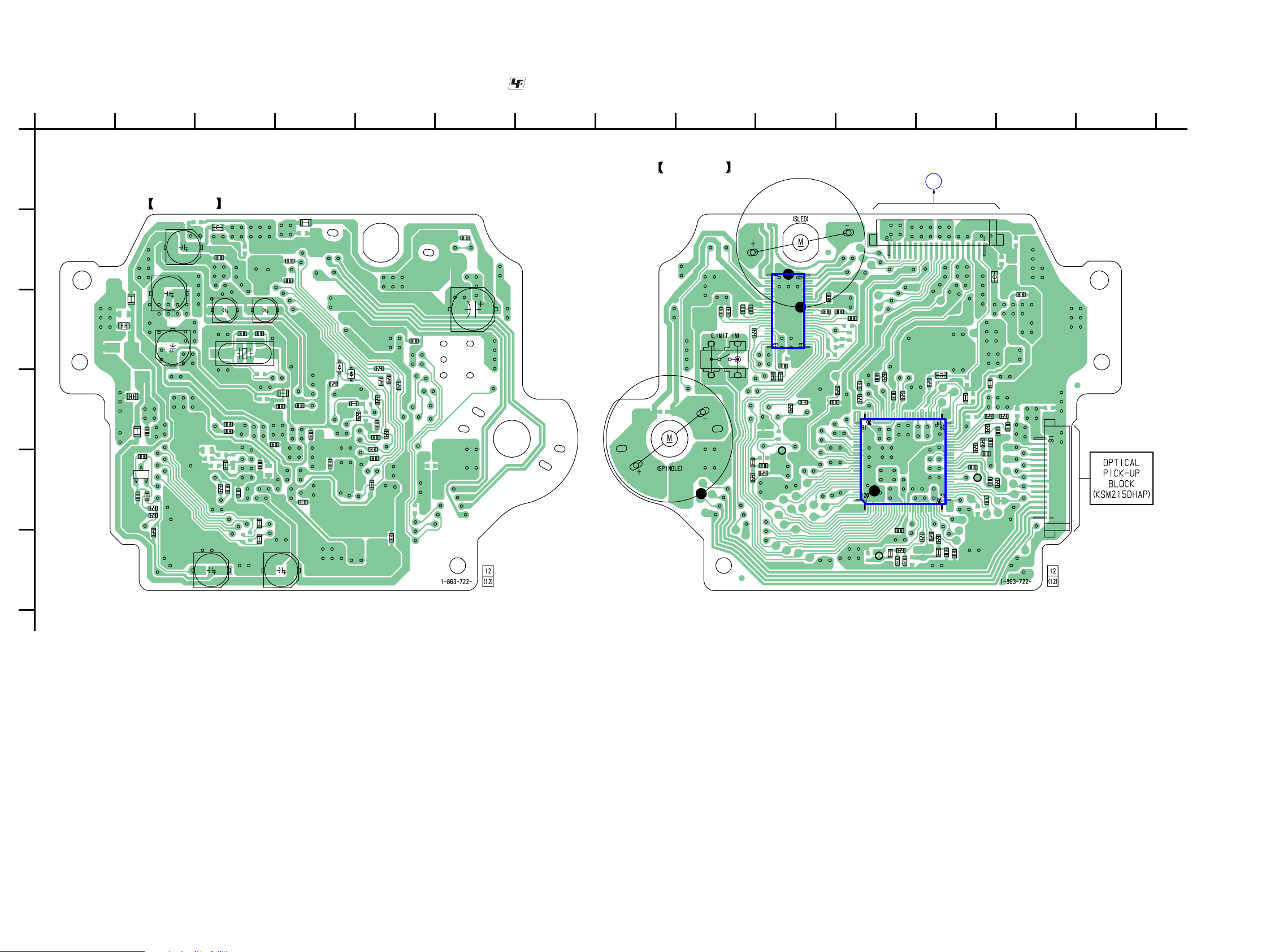
Connecting and Adjustment Location: CD board
– CD BOARD (CONDUCTOR SIDE) –
TP5
(VC)
TP3
(TEI)
TP216
(RFACO)
TUNER SECTION
FM AUTO STOP CHECK
generator
RF signal waveform
VOLT/DIV : 200 mV
TIME/DIV : 500 ns
level : 1.1 ± 0.3 Vp-p
E-F BALANCE (1 TRACK JUMP) CHECK
oscilloscope
CD board
TP3 (TEI)
TP5 (VC)
Procedure:
1. Connect an oscilloscope to TP3 (TEI) and TP5 (VC).
2. Turn the power ON.
3. Load a disc (YEDS-18) and playback the number 5 track.
4. Confi rm that the level B and A (DC voltage) on the oscillo-
scope waveform.
1 track jump waveform
B
center of
waveform
SET
+
75 Ω
Procedure:
1. Turn the power on.
2. Input the following signal from Signal Generator to FM antenna input directly.
* Carrier Freq : A = 87.5 MHz, B = 98 MHz, C = 108 MHz
Deviation : 75 kHz
Modulation : 1 kHz
ANT input : 35 dBu (EMF)
Note: Please use 75 ohm “coaxial cable” to connect SG and the set. You
cannot use video cable for checking.
Please use SG whose output impedance is 75 ohm.
3. Set to FM tuner function and scan the input FM signal with
automatic scanning.
4. Confi rm that input Frequency of A, B and C detected and auto-
matic scanning stops.
The stop of automatic scanning means “The station signal is received in good condition”.
DVC
20
level = 1.3 ± 0.6 Vp-p
A (DC voltage)
symmetry
Page 21
NAS-E35HD/SS-CE35HD
NAS-E35HD/SS-CE35HD
2121
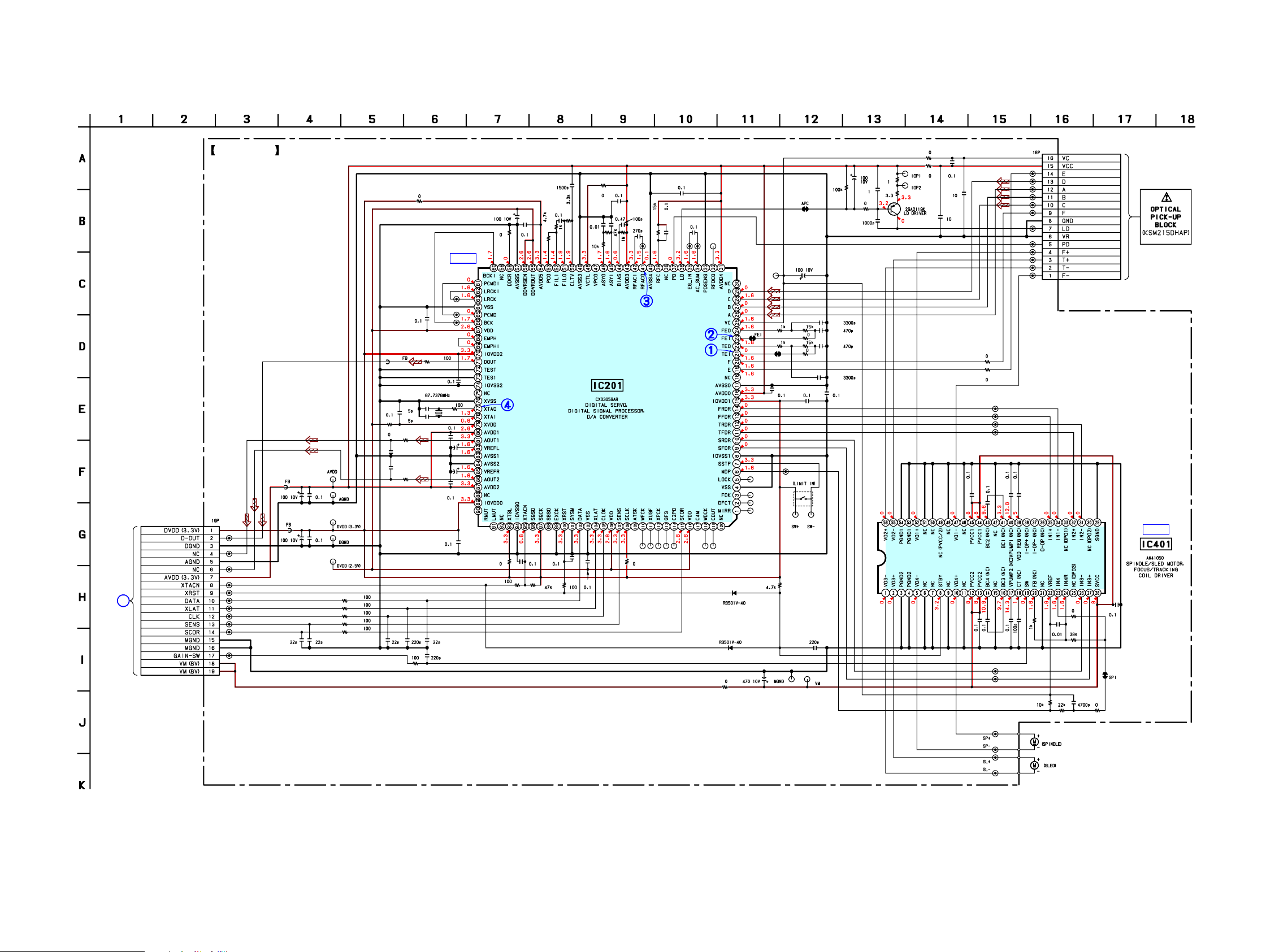
SECTION 6
DIAGRAMS
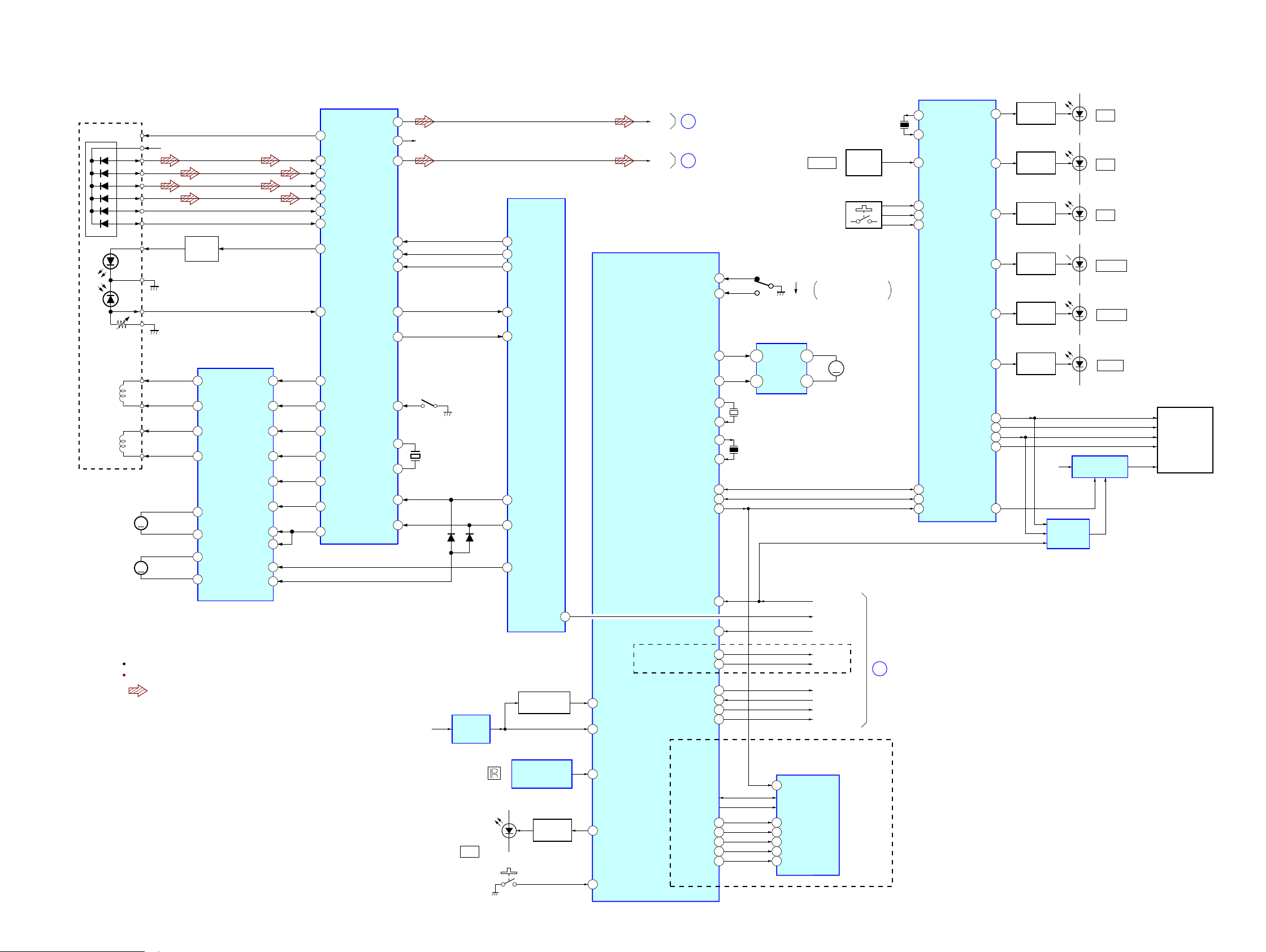
6-1. BLOCK DIAGRAM - CD SERVO, PANEL Section -
USB SYSTEM CONTROLLER
SYSTEM CONTROLLER
IC803 (1/3)
FONT ROM
IC405
IC2 (1/2)
OPTICAL PICK-UP
BLOCK
(KSM215DHAP)
A
B
E
F
LD
VC
CD A +3.3V
GND
PD
VR
LD DRIVER
Q321
FOCUS
COIL
TRACKING
COIL
C
D
IC401
SPINDLE/SLED MOTOR DRIVER,
FOCUS/TRACKING COIL DRIVER
VO1+
52
VO1–
47
VO2+
56
VO2–
55
F–
F+
T–
T+
+
–
+
–
35
IN1+
34
IN1–
32
IN2+
31
IN2–
27
IN3+
26
IN3–
24IN4R
19SW
MDP
6
SRDR
10
SFDR
9
TRDR
12
TFDR
11
FRDR
14
FFDR
13
8STBY
DIGITAL SERVO, DIGITAL SIGNAL PROCESSOR, D/A CONVERTER
IC201
71
DOUT
104XLAT
115
SCOR
7
SSTP
78
XTAI
77
XTAO
100
XRST
S201
(LIMIT IN)
X201
D441D440
67.7376MHz
BD_XLAT
BD_GAIN–SW
BD_XTACN
BD_SCOR
BD_XRST
107
SENS
BD_SENS
VC
25
A
26
B
27
C
28
D
29
E
19
F
20
LD
36
PD
37
23IN4
95
XTACN
102DATA
BD_DATA
BD_CLK
105
120
122
117
121
116
CLOK
VO4+
M
VO4–
M401
(SPINDLE)
VO3+
M
VO3–
M402
(SLED)
10
5
2
1
CD LOADING
MOTOR DRIVE
IC805
2
9
7
4
44
CDM OPEN SW
45
CDM CLOSE SW
43
CDM LOAD IN
42
CDM LOAD OUT
M
+
–
S001
CD TRAY
OPEN/CLOSE DETECT
M001
(LOADING)
CLOSE
OPEN
I–I+O–
O+
135
130
119
AOUT1
AOUT2
R-CH
CD-L
: CD PLAY
SIGNAL PATH
R-ch is omitted due to same as L-ch.
A
DOUT
B
86
81
FLUORESCENT
INDICATOR TUBE
FL401
30 IIC_DATA
29 IIC_CLK
12 RESET
(UK)
36VFD_LAT
35
37
38
VFD_DATA
VFD_CLK
VFD_BK
4VFD_POWER
+18V
+3.3V
3GC_RESET
30
29
IIC_DATA
IIC_CLK
85AC_DET
D0 - D14, D15/A-1
A0 - A17
26 CE50XCS
D0 - D15
A1 - A17, A19
16 A1849XCS1
9A1948XCS2
11 WR46NO USE
28 OE44XRD
97 KEY0
95 KEY1
94 KEY2
DISPLAY CONTROLLER
IC403
X401
5MHz
XOUT
XIN
13
15
X801
32.768kHz
XCOUT
XCIN
11
10
X802
5MHz
XOUT
XIN
13
15
VOL
VOLUME
92
SIRCS
4
ROTARY
ENCODER
S602
REMOTE CONTROL
RECEIVER
IC601
AC CUT
20
RESET
12
VOLTAGE
DETECT
IC801
REGULATOR
IC402, Q401 - 408
S601, 603 - 609,
S611 - 621
I/
STANDBY LED
37
LED DRIVE
Q601
RESET SWITCH
Q801
D601
D610
D601, S610
HDD
LED_HDD
18
LED DRIVE
Q410
D410
USB
LED_USB
19
LED DRIVE
Q411
D411
CD
LED_CD
20
LED DRIVE
Q412
D412
AUDIO IN
LED_AUDIO_IN
21
LED DRIVE
Q413
D413
DMPORT
LED_DM_PORT
22
LED DRIVE
Q414
D414
TUNER
LED_TUNER
23
LED DRIVE
Q415
D415
KEY_WAKE_UP_
POWER
74
4
CD-PO
CD-PO
F
(Hong Kong, Taiwan, Korean, Chinese)
AC_DET
84I_POWER_PROTECT
P MONI
49DAB_POWER_1.2
DAB_1.2V
50DAB_POWER_3.3
DAB_3.3V
80DM_EN
DM_EN
76XDM_PROTECT
DM_PROTECT
34GENESIS POWER
HDD ON
87POWER_ON
POWER_ON
12 NC
REGULATOR
CONTROL
IC401
(Page 23)
(Page 22)
(Page 24)
Ver. 1.1
Page 22
NAS-E35HD/SS-CE35HD
NAS-E35HD/SS-CE35HD
2222
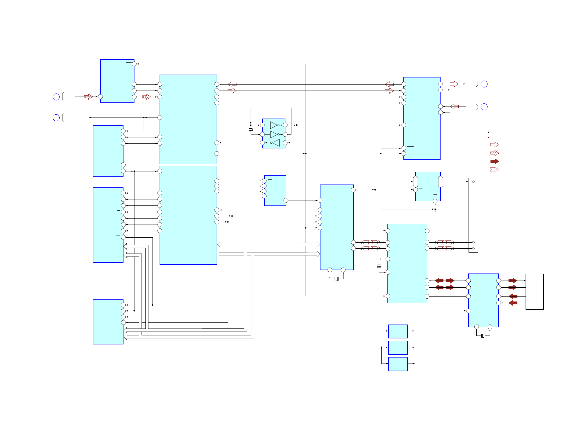
6-2. BLOCK DIAGRAM - USB, HDD Section -
10
LRCKO
RST
11
21
BCKO
20
RXIN
DATA BUFFER
IC11
SYSTEM
CONTROLLER
IC803 (2/3)
DOUT
12
DOUT
8DOUT
9DIN
SDTI
12 BCK
11 SYSCK
13 PDAD
BCKO
17
CLKIN
14 PDAA11
D_RESET
46 xINT126
USB_INT
44 xWR38
EM_WE
43 xRD
40 xRESET
45 xCS
22DP
12DM
1
7
6
104
EM_OE
4G2A
13Y2
100
EM_CS (2)
1A107
A
2B105
B
15 Y0
SDTO_O
LRCKO
10 LRCK
LIN
LOUT
R–CH
R–CH
111 I2CO_SDA/BOOT
127 AC_DET
108 I2CO_SCL/BOOT
31
GENESIS IIC_DATA
36
GENESIS AC DET
32
GENESIS IIC_CLK
38
USB VBUS ON
35
GENESIS RESET
XRESET
SDRAM
IC3
USB SYSTEM CONTROLLER
IC2 (2/2)
USB INTERFACE
IC4
A/D CONVERTER, D/A CONVERTER
IC12
USB POWER CONTORL
IC14
HARD DISK DRIVER
IC9
MEMORY DECODER
IC7
INVERTER
IC10
X2
22.5792MHz
3914EM_WE_DQM (0)
EM_CAS
EM_RAS
EM_CS (0)
EM_CKE
EM_CLK
EM_WE_DQM (1)
37
98
15
LDQM
17
CAS
FLASH MEMORY
IC1
EM_D (0)
– EM_D (15)
EM_A (0_1)
– EM_A (_19)
EM_BA (0)
, EM_BA (1)/EM_A (_0)
12
RST#
VBUS
11
WE#
26
CE#
28
OE#
12
RESET#
18
RAS
97
71
19
CS
37
CKE
70
67
38
CLK
39
UDQM
16
WE
DQ0 – DQ15
A0 – A11
BS0, BS1
Q0 – Q15
A0 – A19
8BCKI
134 SDTO_ I
8
3
J852
(USB)
2
1
OUTIN
D+
D–
VBUS
GENESIS +5V
2
3
12 LRCKI
15VOUTL
16VOUTR
3VINL
2VINR
31 USBUP_DP
30 USBUP_DM
USB 2.0 HUB CONTROLLER
IC13
2USBDN1_DP
12PRTPWR1
1USBDN1_DM
USBDN2_DP
USBDN2_DM
19VBUSHF
5OC
GENESIS +2V
GENESIS +5V
+1.2V
REGULATOR
IC5
GENESIS +1.2V
GENESIS +3.3V
GENESIS +2.5V
D0 – D15
D0 – D15
A0_1 – A_19, BA0, BA1_A0
A0_1 – A6_7, BA1_A0
113
115
144
142
5
+3.3V
REGULATOR
IC6
CD0 – CD15
CA0 – CA7
+2.5V
REGULATOR
IC8
: TUNER (FM/AM)
SIGNAL PATH
R-ch is omitted due to same as L-ch.
D
E
B
GENESIS AC DET
C
: CD PLAY
: HDD
: USB
HARD
DISK
DRIVE
18
XTALO17XTALI
X5
12MHz
31XO32
XI
4
EN
X1
12MHz
32
XTAL2
33
XTAL1/CLKIN
X4
24MHz
27RXP
28RXN
32TXP
31TXN
4
3
20
16PRTPWR2 13
19DPDM
26
RESET_N
2, 3
6
−
8
13 OCS1_N
(Page 21)
(Page 24)
(Page 23)
(Page 23)
Page 23
NAS-E35HD/SS-CE35HD
NAS-E35HD/SS-CE35HD
2323
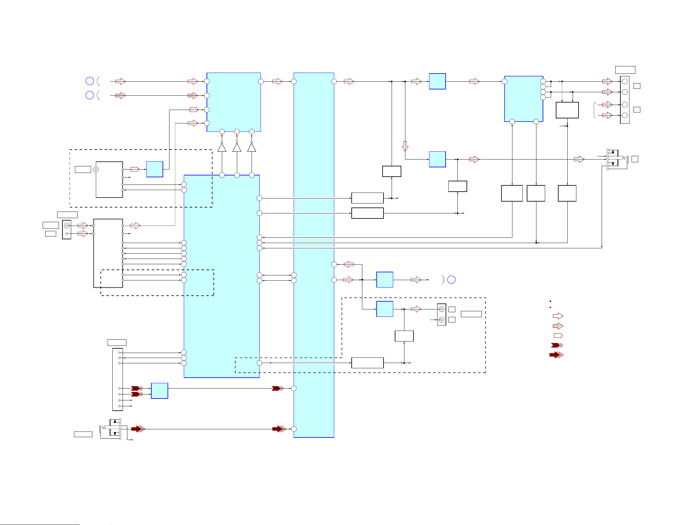
6-3. BLOCK DIAGRAM - MAIN Section -
IN-L1
1
INPUT SELECTOR, ELECTRICAL VOLUME
IC302
IN-L2
3
VOL L
11
SEL L
10
OUT L
23
X2
15
X3
11
INPUT SELECTOR
IC351
X
13
R-CH
IN-L3
5
R-CH
J301
AUDIO IN
X0
12
LIN
D
LOUT
E
X1
14
CD-L
A
L
R
J303
SPEAKER
+
–
R-CH
+
–
J
J302
TUNER (FM/AM)
AM
ANTENNA
FM ANT
AM ANT
L-OUT
R-OUT
DO/STEREO
R-CH
DI
CLK
CE
FM 75Ω
DAB 75Ω
93 ST DATA IN
TUNED
6 ST TUNED
95 ST DATA OUT
94 ST CLK
92 ST CE
RDS DATA
RDS INT
7 RDS DATA
18 RDS-INT
J304
L
R
R-CH
AUDIO OUT
J811
DMPORT
(AEP, UK)
6
5
7
DET
RXD
TXD
12
R- R-CH
14
R+ R-CH
11
L-
13
L+
79 DMPORT DET
77 CLINK_TXD_OUT
78 CLINK_RXD_IN
LINE
AMP
IC305
DAB TUNER MODULE
DAB601
AUDL
J601
AUDR
S1_DOUT
R-CH
S1_DIN
48 DAB RXD_IN
47 DAB TXD_OUT
(UK)
(Hong Kong, Taiwan, Korean, Thai, Australian, Chinese)
LINE
AMP
IC304
LINE
AMP
IC306
LINE
AMP
IC303
1
INH
6
INH
Q305
97
SEL A
10
A
Q306
100
SEL B
9
B
Q307
SYSTEM CONTROLLER
IC803 (3/3)
SDA
26
SCL
25
24VOL IIC_DATA
22VOL IIC_CLK
MUTING CONTROL
Q308, 309
MUTING
Q111
REC MUTE
25
R-CH
MUTING CONTROL
Q303, 304
MUTING
Q115
TA LINE-MUTE
23
R-CH
R-CH
R-CH
MUTING CONTROL
Q301, 310
MUTING
Q102
HP MUTE
21
LINE
AMP
IC301
LINE
AMP
IC307
HP DET
DAMP_PROTECT
DAMP_SHUTDOWN
PROTECT
SWITCH
Q352
OVER LOAD
DETECT
Q151, 152
5
SHUTDOWN
LINP
21LOUTN
19
20
22
LOUTP
LOUTP
LOUTN
4644
FAULT
DIGITAL POWER AMP
IC352
SHUT DOWN
SWITCH
Q353
PROTECT
SWITCH
Q355
2
28
27
: TUNER (FM/AM)
SIGNAL PATH
R-ch is omitted due to same as L-ch.
: CD PLAY
: DAB
: DMPORT
: AUDIO IN
(Page 22)
(Page 21)
(Page 22)
Ver. 1.1
Page 24
NAS-E35HD/SS-CE35HD
NAS-E35HD/SS-CE35HD
2424
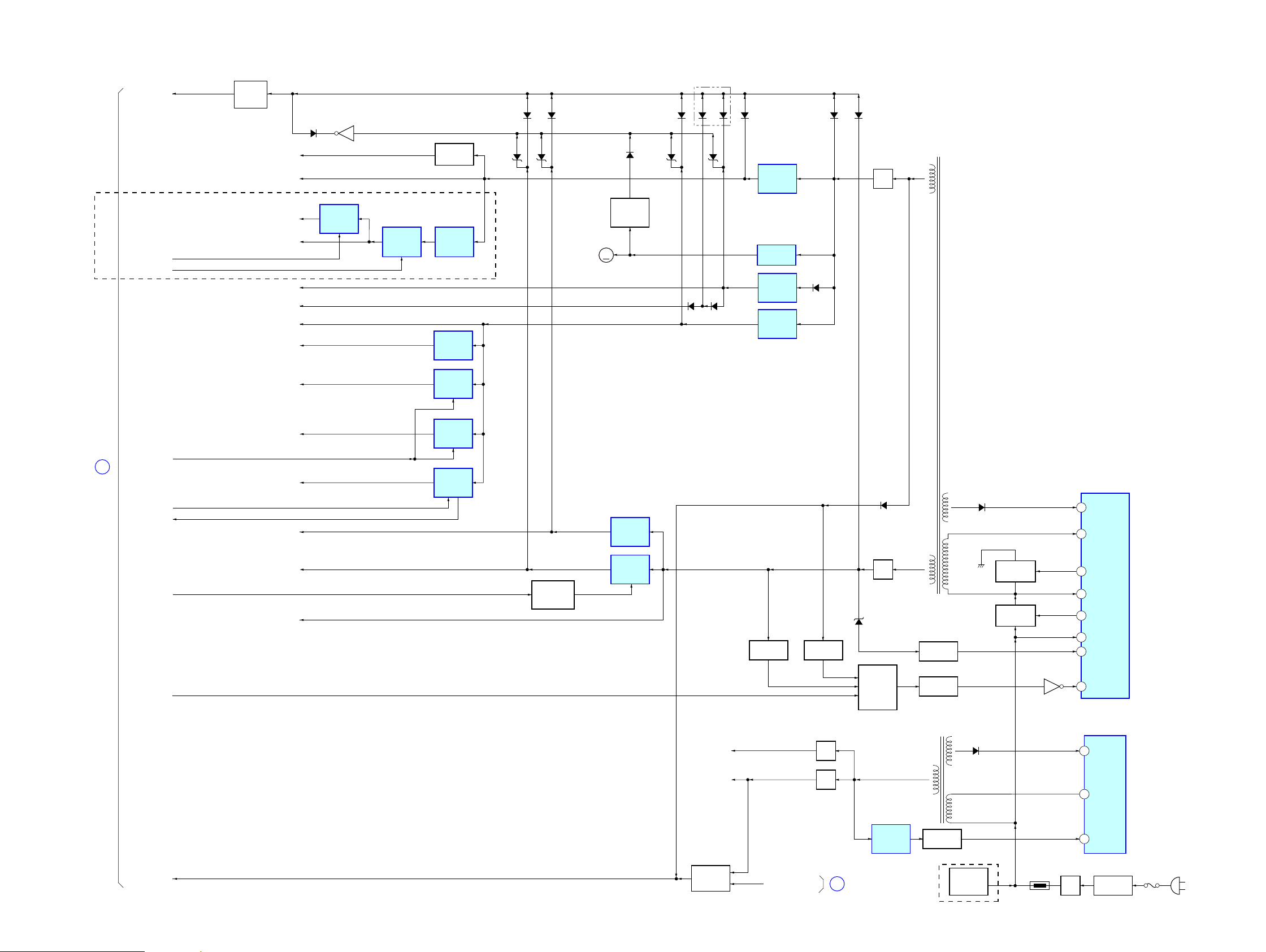
6-4. BLOCK DIAGRAM - POWER SUPPLY Section -
F
Q904
P MONI
PROTECT
SWITCH
Q802
D918
D922
D926 D927
POWER CONTROL
IC02
D13
D06
+3.3V
(AC IN)
F01
LINE FILTER
T01
VOLTAGE
SELECTOR
S1
RECT
D01
TH01
D923
D924
D920
D915, 916
D917
15 VS
18 VD
1 VSENSE
2 F/B
16 VG (H)
12 VG (L)
8VC1
POWERCONTROL
IC01
5 DRAIN
2FB
4VCC
ISOLATOR
PC04
ISOLATOR
PC03
ISOLATOR
PC01
T03
MAIN POWER
TRANSFORMER
T02
SUB POWER
TRANSFORMER
RECT
D808
IC803 +3.3V
POWER
ON/OFF
CONTROL
SWITCH
Q901, 908
SWITCHING
Q02
SWITCHING
Q01
SHUNT
REGULATOR
IC901
RECT
D902
DAB_1.2V
DAB_3.3V
REGULATOR
IC905
M901
(FAN)
SWITCHING
REGULATOR
IC902
POWER_ON
Q03
9OCP
D304
FAN STOP
DETECT
Q905, 906
DC DETECT
Q354
DC DETECT
Q902, 903
AC DETECT
Q803, 804
MM
DAB +3.3V
DAB +1.2V
+12V
+8V
+18V
+5V
GENESIS +5V
+3.3V
REGULATOR
IC651
+5V
REGULATOR
IC653
IC301 B+
REGULATOR
Q302
+1.2V
REGULATOR
IC652
DM_EN
HDD ON
DM_PROTECT
DMP +5V
+5V
REGULATOR
IC802
CD-PO
DISPLAY +3.3V
+3.3V
REGULATOR
IC404
CD D +3.3V
CD A +3.3V
(UK)
(Chilean, Peruvian, Brazilian)
RECT
D807
AC_DET
GENESIS AC DET
C
+3.3V
REGULATOR
IC982
+3.3V
REGULATOR
IC981
SWITCHING
REGULATOR
IC907
REGULATOR
CONTROL
Q907, 909
SWITCHING
REGULATOR
IC904
GENESIS +2V
SWITCHING
REGULATOR
IC906
+9V
+9V
REGULATOR
IC908
RECT
D903
D925
D913
D928
D906
D912
D905
D914, 929
D919
(Page 21)
(Page 22)
Ver. 1.1
Page 25
NAS-E35HD/SS-CE35HD
NAS-E35HD/SS-CE35HD
2525
For Schematic Diagrams.
Note:
• All capacitors are in μF unless otherwise noted. (p: pF) 50
WV or less are not indicated except for electrolytics and
tantalums.
• All resistors are in Ω and 1/4 W or less unless otherwise
specifi ed.
• f : internal component.
• 2 : nonfl ammable resistor.
• C : panel designation.
THIS NOTE IS COMMON FOR PRINTED WIRING BOARDS AND SCHEMATIC DIAGRAMS.
(In addition to this, the necessary note is printed in each block.)
• A : B+ Line.
• Voltages and waveforms are dc with respect to ground
under no-signal conditions.
– CD Board –
no mark
: CD PLAY
– USB MICOM Board –
no mark
: USB PLAY
– Other Boards –
no mark
: TUNER (FM/AM)
( ) : CD PLAY
‹‹ ›› : USB PLAY
• Voltages are taken with VOM (Input impedance 10 MΩ).
• Circled numbers refer to waveforms.
• Signal path.
F : TUNER (FM/AM)
J : CD PLAY
i : AUDIO IN
f : HDD
d : DAB
a : USB
l : DMPORT
• Abbreviation
AR : Argentina model
AUS : Australian model
BR
: Brazilian model
CH : Chinese model
E51 : Chilean and Peruvian models
HK : Hong Kong model
KR : Korean model
MX : Mexican model
RU : Russian model
TH : Thai model
TW : Taiwan model
For Printed Wiring Boards.
Note:
• X : Parts extracted from the component side.
• Y : parts extracted from the conductor side.
• f : internal component.
• : Pattern from the side which enables seeing.
(The other layers' patterns are not indicated.)
• Indication of transistor.
Caution:
Pattern face side:
(SIDE B)
Parts face side:
(SIDE A)
Parts on the pattern face side seen from
the pattern face are indicated.
Parts on the parts face side seen from
the parts face are indicated.
Caution:
Pattern face side:
(Conductor Side)
Parts face side:
(Component Side)
Parts on the pattern face side seen from
the pattern face are indicated.
Parts on the parts face side seen from
the parts face are indicated.
• USB MICOM board is multi-layer printed board.
However, the patterns of intermediate-layers have not
been included in diagrams.
• Circuit Boards Location
Ver. 1.1
Note:
The components identifi ed by mark 0 or dotted
line with mark 0 are critical for safety.
Replace only with part
number specifi ed.
C
Q
B
E
Q
B
CE
These are omitted.
These are omitted.
CD board
MOTOR board
KEY (L) board
HP JACK board
D/D CON board
MAIN board
DISPLAY board
KEY (FRONT) board
USB JACK board
DMP board
POWER board
SP TEMINAL board
D-AMP board
USB MICOM board
DAB board (UK model)
KEY (R) board
Page 26
NAS-E35HD/SS-CE35HD
NAS-E35HD/SS-CE35HD
2626
6-5. PRINTED WIRING BOARD - CD Board -
• : Uses unleaded solder.
• See page 25 for Circuit Boards Location.
1
A
B
C
D
E
F
234567891011121314
R326
R325
C323
C401
R401
C208
C214
C267
C268
C322
R323
R322
R321
R324
CD BOARD
(COMPONENT SIDE)
CD BOARD
(CONDUCTOR SIDE)
R201
C211
C321
R301
C212
C213
R203
C202
C218
C219
C205
C220
R276
R275
C271
C201
C270
C269
C203
R272
R277
C272
C215
R278
C232
R105
R104
R101
R102
C102
C101
X201
C104
C105
C302
C303
R260
C210
Q321
C207
R302
C301
C257
R256
C404
D440
D441
R440
C440
C403
CN301
IC201
C259
R257
C258
C260
C261
R258
R259
R206
C206
R202
CN101
MAIN BOARD
CNP804
V
R265
R266
R267
C264
C265
C204
C103
R103
R292
R268
R106
C106
C256
C254
C253
C251
C252
R254
R255
R252
R253
R279
R280
C217
C291
C292
R269
R270
R291
R426
C425
TP5 (VC)
TP3 (TEI)
TP216
(RFACO)
C422
C428
C429
C430
C405
R425
R281
R432
IC401
C421
R421
C423
C424
R422
R423
M402
M401
S201
(Page 37)
Page 27
NAS-E35HD/SS-CE35HD
NAS-E35HD/SS-CE35HD
2727
6-6. SCHEMATIC DIAGRAM - CD Board -
• See page 43 for waveforms. • See page 54 for IC Block Diagrams.
IC B/D
IC B/D
R256
C259
R257
C261
C208
TP114
C301
TP221
TP3
(TEI)
(VC)
C206
TP215
TP313
R322
R321
TP212
R324
TP1
TP307
TP310
TP306
TP214
TP308
TP209
TP311
TP220
TP305
TP213
TP216
(RFACO)
R265
R266
R267
TP218
TP201
TP210
TP226
TP312
TP224
C212
C213
CD BOARD
C219
C220
TP404
TP405
R103
TP105
R275
TP102
C201
TP205
TP106
C203
TP101
TP314
R272
R106
R277
C272
TP206
TP403
TP222
TP227
TP223
TP225
TP207
TP116
TP204
TP115
TP113
TP104
MAIN
BOARD
(3/3)
CNP804
V
TP202
TP219
TP203
TP401
TP211
TP5
TP412
TP411
TP304
R105
R104
R101
R102
R260
C210
TP309
C253
C251
R254R255
R252
R253
TP103
C207
C270
22
6.3V
C269
22
6.3V
TP4
TP303
TP302
TP208
TP406
TP301
TP402
C401
TP112
C202
C204
C258
C214
C232
C215
C267
C268
C321
C254
C252
C264
R258
R269
R291 100
C291 470p
R292 100
C292 470p
TP407
TP408
TP409
TP410
C205
R423
R432
C423
R425
R422
C404
R426
TP2
C425
R421
C424
D440
D441
R440
IC201
X201
R270
C265
C260
C271
C257
C256
C440
C430
C429
C428
R278
R276
C218
C217
R268
C211
R203
R206
C105
C104C103
C106
C102C101
R401
C303
C302
R301
R302
C322
C323
R323
R326
R325
C405
C403
C422
C421
IC401
CN101
CN301
M401
M402
R201
R202
R281
Q321
R280
R279
S201
R259
(Page 35)
Page 28
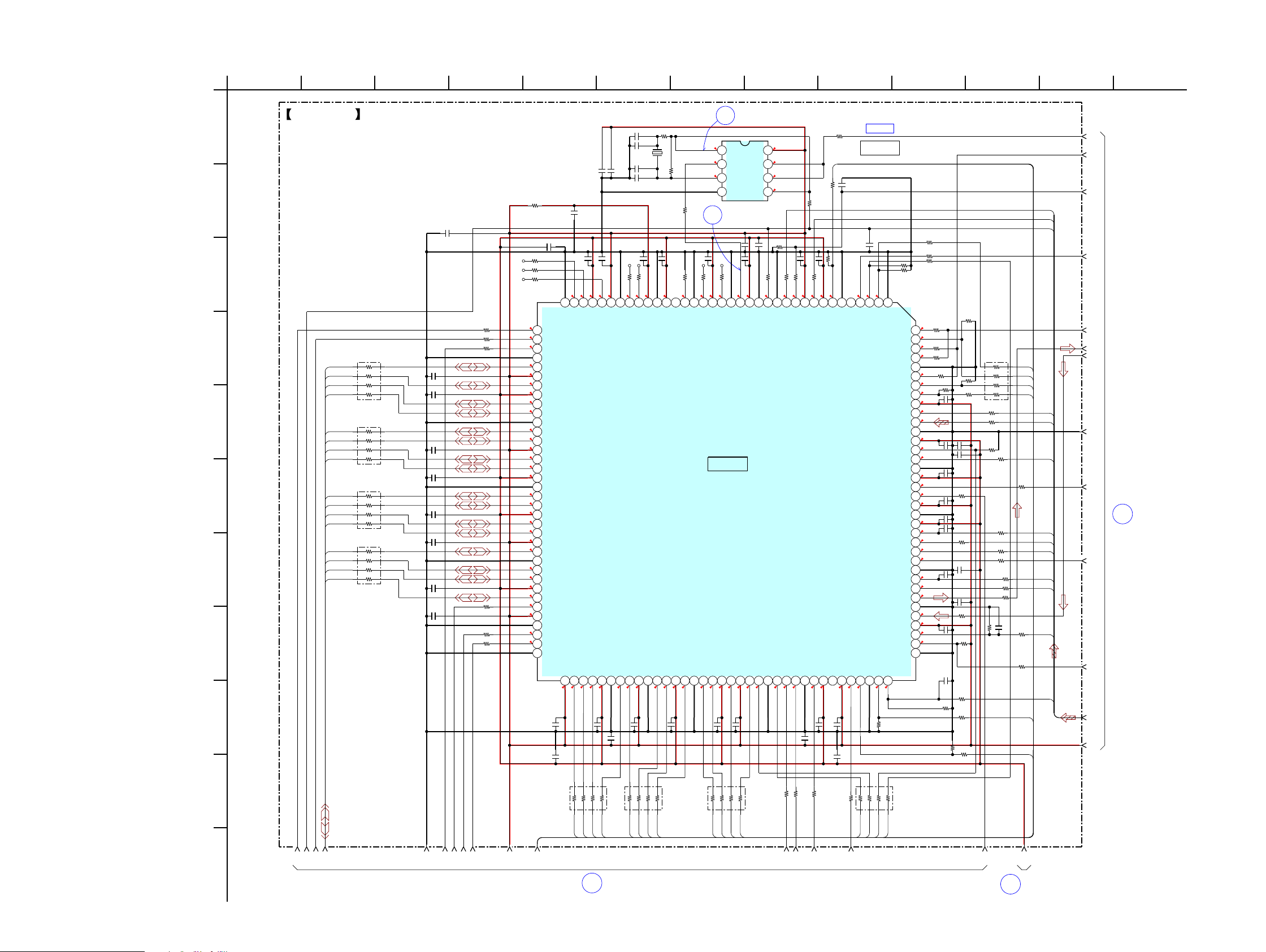
NAS-E35HD/SS-CE35HD
NAS-E35HD/SS-CE35HD
2828
• See page 43 for waveforms. • See page 54 for IC Block Diagrams. • See page 64 for IC Pin Function Description.
6-7. SCHEMATIC DIAGRAM - USB MICOM Board (1/4) -
2
(3/4)
USB MICOM
BOARD
(4/4)
USB MICOM
3
BOARD
(2/4)
USB MICOM
1
BOARD
IC B/D
12
11
J
4
B
6911
D
H
10
K
35 12
C
F
1
E
8
G
A
2
I
7
3. 3
3. 1
1. 2
3. 3
3. 3
3. 3
1. 2
3. 3
3. 3
3. 3
0
1. 203. 3
1. 2
1. 5
3. 3
1. 2
1. 6
3. 3
3. 3
1. 6
3. 3
3. 3
3. 3
3. 3
1. 6
3. 3
1. 6
1. 6
3. 3
0
3. 3
3. 3
3. 3
0
1. 2
1. 2
0
0
3. 3
3. 3
3. 3
1. 2
0
3. 3
3. 3
0
3. 3
0
0
3. 3
0
2. 6
0. 8
3
2. 9
3. 3
2. 4
2. 3
2. 4
1. 2
2. 2
3. 3
2. 4
2. 4
2. 2
0. 5
1. 2
0. 7
2. 1
3. 3
0. 7
1. 2
0. 1
0. 1
0. 8
0. 7
0. 8
1. 2
1. 6
2. 9
3. 3
3. 3
3. 3
0. 2
0. 2
1. 2
1. 2
1. 6
3. 3
2. 6
2. 8
1. 2
1. 6
1. 8
1. 6
0. 1
1. 2
1
0. 2
3. 3
3. 203. 1
3. 1
3. 3
3. 3
1. 2
0
2. 6
3. 3
3. 3
1. 81. 6
1. 8
1. 8
1. 6
1. 5
1. 6
22.5792MHz
X2
0.1
C1
0.1
C15
0.1C16
0.1
C17
0.1C18
0.1C19
0.1C20
0.1C21
0.1
C22
0.1
C23
0.1
C24
0.1
C25
0.1
C26
0.1
C27
0.1
C28
0.1C29
0.1C30
0.1C31
0.1C32
0.1C33
0.1C34
0.1
C35
0.1
C36
0.1
C38
0.1C39
0.1
C40
0.1C43
0.1
C55
0.1
C121
0.1
C123
0.1
C124
10pC130
10p
C133
10
C98
10
C102
10
C103
10
C104
10C105
10C107
10C108
10
C109
10
C110
10C111
10
C112
10
C118
10
C138
100
R64
100
R66
10kR2
10k
R122
10kR124
10k
R125
10k
R126
10k
R127
10k
R128
10kR129
10k
R130
10k
R131
10k
R132
10kR133
10k
R135
10kR136
1M
R1
0R44
0R48
0
R49
0
R50
0R51
0
R62
0R63
0
R67
0R68
0
R71
0
R96
0
R117
0R118
0R119
0
JR7
R74
0
100R65
47
R40
100
R73
47
R72
47
R69
100
R60
100
R56
47
RB6
21
43
65
87
21
43
65
87
21
43
65
87
21
43
65
87
47
RB13
47
RB5
47
RB4
47
RB3
2143658
7
47
RB2
2143658
7
47
RB12
2143658
7
47
RB11
2143658
7
47
RB1
2
4
6
8
1
3
5
7
100
R82
100R53
100R57
100R58
100R59
100R61
5pC131
5p
C132
12345678
9101112131415161718192021222324252627282930313233343536
37
38
39
40
41
42
43
44
45
46
47
48
49
50
51
52
53
54
55
56
57
58
59
60
61
62
63
64
65
66
67
68
69
70
71
72
73 74 75 76 77
78
79
80
81 82 83 84
85
86
87
88
89
90
91 92
93 94
95
96
97 98
99
100 101 102
103
104
105
106
107
108
109
110
111
112
113
114
115
116
117
118
119
120
121
122
123
124
125
126
127
128
129
130
131
132
133
134
135
136
137
138
139
140
141
142
143
144
100
R154
100
R43
100
R116
100p
C163
100p
C164
10C106
B01
B02
B03
B04
GND
B06
B07
B08
B09
3.3V
A01
A02
B11
B13
B14
B15
B17
D01
A04
A03
A05
A06
B18
B16
3.3V
A07
A09
A10
A11
GND
A_19
A_18
A_17
A_16
A_15
CA1
CA2
A11_12
A9_10
A8_9
A7_8
A6_7
A5_6
A4_5
A3_4
A2_3
A1_2
A0_1
A10_11
BA1_A0
BA0
D0
D1
D2
D3
D4
D5
D6
D7
D8
D9
D10
D11
D12
D13
D14
D15
A_13
A_14
EM_CAS
EM_WE
EM_WE_DQM(0)
VSS
EM_D(7)
DVDD
EM_D(6)
EM_D(5)
EM_D(4)
VSS
EM_D(3)
EM_D(2)
DVDD
EM_D(1)
EM_D(0)
CVDD
VSS
EM_D(15)
EM_D(14)
CVDD
EM_D(13)
EM_D(12)
DVDD
EM_D(11)
VSS
EM_D(10)
EM_D(9)
CVDD
EM_D(8)
EM_WE_DQM(1)
DVDD
VSS
EM_CLK
EM_CKE
VSS
CVDD
1A
3Y
2A
GND
USB MICOM BOARD (1/4)
LRCK
BCK
RESET
SDA
CLK
SENS
XLAT
DATA
SCOR
XTACN
SDTO
XRST
SCL
R55 0
IC10
INVERTER
R26 0
R27 0
R28 0
R32 0
R29 0
R31 0
R33 0
4321
5678
2Y
3A
1Y
Vcc
TC7WHU04FU(TE12R)
IC10
R36 100
R37 0
R39 0
R38 0
R105 0
100p
C160
100p
C161
VSS
EM_A(_18)
EM_A(_13)
CD-PO
MCK
VSS
EM_A(_19)
CVDD
BCKI
DVDD
D_RESET
LRCKI
VSS
XRESET
VSS
CVDD
CLKIN
VSS
TMS
CVDD
XTRST
OSCVSS
OSCIN
OSCOUT
OSCVDD
VSS
PLLHV
TDI
TDO
VSS
DVDD
EMU0
CVDD
EMU1
TCK
VSS
DVDD
EM_A(11_12)
EM_A(9_10)
EM_A(8_9)
CVDD
VSS
EM_A(7_8)
EM_A(6_7)
DVDD
VSS
EM_A(5_6)
EM_A(4_5)
CVDD
EM_A(3_4)
VSS
EM_A(2_3)
EM_A(1_2)
CVDD
EM_A(0_1)
DVDD
EM_A(10_11)
EM_BA(1)/EM_A(_0)
VSS
EM_BA(0)
EM_CS(0)
EM_RAS
VSS
EM_CS(2)
CVDD
EM_RW
DVDD
EM_OEBA
I2CO_SCL/
BOOT
VSS
VSS
GPIO/BOOT
I2CO_SDA/BOOT
DVDD
SDTI
VSS
SDTO_O
BD_CLK
BD_SENS
VSS
BD_GAIN-SW
BD_XLAT
BD_DATA
BD_SCOR
CVDD
VSS
DVDD
USB_INT
AC_DET
CVDD
VSS
BD_XTACN
EM_A(_14)
CVDD
VSS
SDTO_I
BD_XRST
EM_A(_15)
EM_A(_16)
ACLKR0
BCKO
VSS
AFSR0
EM_A(_17)
LRCKO
DVDD
IC2
D708E001BRFP266
IC2
USB SYSTEM CONTROLLER
R76 0
R77 22
R121 47
R79 47
R120 47
R78 22
C37
0.1
C42
0.1
13
(Page 30) (Page 31)
(Page 29)
Page 29
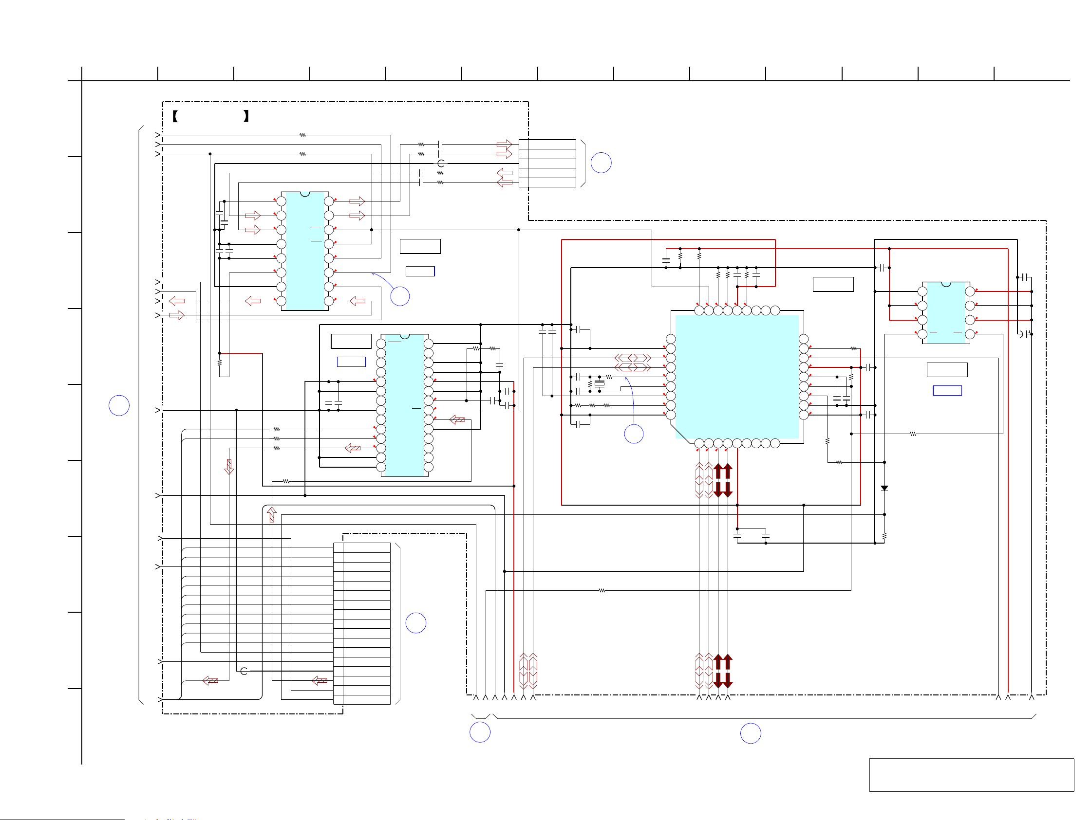
NAS-E35HD/SS-CE35HD
NAS-E35HD/SS-CE35HD
2929
• See page 43 for waveforms. • See page 54 for IC Block Diagrams. • See page 64 for IC Pin Function Description.
6-8. SCHEMATIC DIAGRAM - USB MICOM Board (2/4) -
MAIN
(3/3)
CNP302
BOARD
T
(3/4)
USB MICOM
BOARD
5
MAIN
(3/3)
CNP805
BOARD
S
USB MICOM
(1/4)
BOARD
1
(4/4)
USB MICOM
4
BOARD
IC B/D
IC B/D
IC B/D
14
15
1. 61. 6
1. 6
1. 6
3. 3
3. 3
0. 8
3. 3
3. 3
1. 6
1. 8
1. 6
0
1. 6
1. 6
1. 6
0
3. 3
0
3. 3
0
3. 3
3. 3
3. 3
1. 8
3. 3
3. 3
3. 3
0
4. 7
3. 3
3. 300
3. 3
0
0
2. 8
0. 9
0. 9
1. 8
1. 2
3. 3
0
3. 1
0
3
4. 9
3. 3
4. 9
4. 9
4. 9
3. 3
4. 9
IC12 AK4554VT
0.1
C2
0.1
C77
0.1
C117
0.1
C139
0.1
C149
10V
100
C158
10
C78
10
C115
10C116
10
C140
10kR140
0
R83
4.7k
R085
24MHz
X4
10
C120
100k
R22
100k
R21
100k
R20
100k
R23
100k
R19
0.1
C74
0.1C14
0.1
C73
0.1
C72
0.1
C71
0.1
C76
0.1
C70
10
C125
10
C126
10
C119
10
C127
1MR35
22pC128
10kR24
1
2
3
4
5
5P
CN2
0.1
C75
0.1
C159
1
2
3
4
5
6
7
8
9
10
11
12
13
14
15
16
17
17P
CN3
1kR25
1kR86
100R137
100R138
100R139
100
R88
10k
R145
10kR144
10p
C129
MA2J1110GLS0
D1
100k
R155
0
R157
1k
R142
0
R143
1000p
C146
0.01
C147
A02
A01
3.3V
D06
D08
D09
D10
D11
D12
D13
D14
D04
D02
A04
A03
A05
A07
A06
A09
A10
A11
D01
3.3V
D01
GND
D15
D16
SDTO
RESET
SDA
LRCK
BCK
CLK
XTACN
DATA
XLAT
SCOR
SENS
XRST
SCL
LIN
RIN
GND
LOUT
ROUT
CLK
XTACN
RW-GAIN SW
DATA
XLAT
SCOR
SENS
XRST
SCL
SDA
RESET
CD-PO
DEMP
GND
DOUT
AC_DET
HDD_DET
VCOM
VINR
VINL
GND
Vcc
DEM0
DEM1
DOUT
AUDIO
FSOUT0
FSOUT1
SCKO
VDD
DGND
XTO
XTI
CLKST
LRCKO
BCKO
DOUT
PSCK0
PSCK1
USBDN1_DM
U SBDN1_DP
USBDN2_DM
U SBDN2_DP
VDDA33NCNCNCNC
SUSP_IND/
LOCAL_PWR/
NON_REM0
VDDA33
USBUP_DM
USBUP_DP
XTAL2
XTAL1/CLKIN
VDD18PLL
RBIAS
VDD33PLL
EN
GND
IN
IN
USB MICOM BOARD (2/4)
IC11 DIR9001S1PWRG4
IC11
DATA BUFFER
FB4
0
JR4
IC14
USB POWER CONTROL
5678
4321
OC
OUT
OUT
OUT
IC14
TPS2051BDRG4
IC13
USB2512-AEZG
IC13
USB 2.0 HUB CONTROLLER
NC
NC
NC
SDA/SMBDATA/NON_REM1
VDD33
SCL/SMBCLK/CFG_SEL0
HS_IND/CFG_SEL1
RESET_N
VBUS_DET
OCS1_N
VDDA33
TEST
PRTPWR1
VDD18
VDD33CR
PRTPWR2
OCS2_N
NC
12345678
9
10
11
12
13
14
15
16
17
18
2021222324252627 19
29
30
31
32
33
34
35
36
28
COUT
UOUT
BFRAME
RSV
RXIN
EMPH
RST
FILT
AGND
Vcc
FMT0
FMT1
ERROR
CKSEL
2827262524232221
201918171615
14 13 12 11 10 9 87654321
IC12
A/D CONVERTER,
D/A CONVERTER
DIN
LRCK
SYSCK
BCK
PDAD
PDDA
VOUTL
VOUTR
87654321
161514131211109
R123 0
R75 0
0.47
C142
100
R109
1
C144
100
R108
C141 0.47
R107 100 C145 1
R110 100
FB3
R30 0
4
B
6911
D
H
1035 12
C
F
1
E
8
G
A
2 13
I
7
Note: IC13 on the USB MICOM board cannot exchange
with single. When IC13 on the USB MICOM board
is damaged, exchange the entire mounted board.
(Page 28)
(Page 35)
(Page 35)
(Page 30)
(Page 31)
Page 30
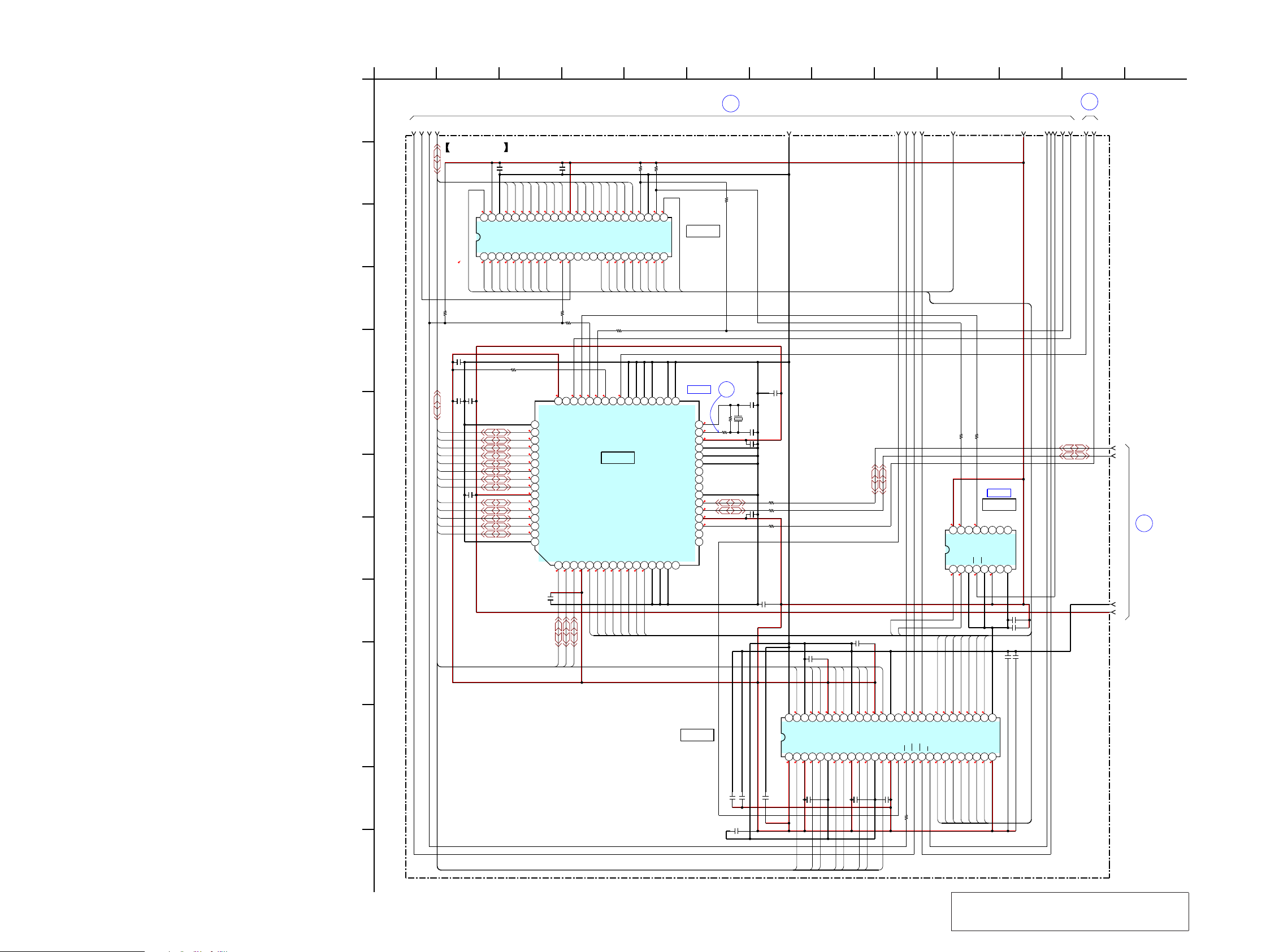
NAS-E35HD/SS-CE35HD
NAS-E35HD/SS-CE35HD
3030
• See page 43 for waveforms. • See page 54 for IC Block Diagrams.
6-9. SCHEMATIC DIAGRAM - USB MICOM Board (3/4) -
(4/4)
USB MICOM
6
BOARD
(2/4)
USB MICOM
5
BOARD
(1/4)
USB MICOM
BOARD
2
IC B/D
IC B/D
3. 30
3. 3
3. 3
3. 3
3. 3
3. 3
3. 3
3. 3
3. 333. 3
3. 3
3. 3
1
2. 6 0. 8
2. 5
0
0
3. 3
3. 3
0. 7
0. 1
0. 2
0. 1
0. 2
0. 7
0. 2
2. 5
2. 4
2. 2
2. 3
2. 4
2. 4
2. 4
0. 5
2. 2
3. 3
2. 6
1. 6
1. 2
1. 6
1. 810. 1
0. 3
2. 1
3. 3
0. 7
0. 7
3. 3
0. 7
0. 3
0. 1
0. 8
3. 3
0. 8
2. 9
0. 2
1. 6
3. 3
2. 6
0. 2
1. 6
1. 2
2. 8
1. 2
2. 2
3. 3
0. 5
2. 3
2. 3
2. 4
2. 3
2. 2
2. 3
2. 2
3. 3
2. 933. 1
3. 103. 1
3. 1
0. 2
0. 111. 8
1. 6
3. 3
3. 3
3. 3
3. 3
0. 7
2. 6
2. 4
2. 2
0. 1
2. 3
0. 7
0. 1
0. 8
2. 4
2. 4
2. 4
0. 7
3. 3
3. 3
0. 5
3. 1
0. 8
2. 2
3. 3
3. 300. 2
0. 2
0. 2
1. 2
2. 8
3. 3
3. 3
3. 3
3
0
1. 8
1. 6
1. 6
1. 6
1. 6
1
0. 1
0.1C5
0.1
C10
0.1
C44
0.1
C48
0.1C49
0.1C50
0.1C51
0.1
C52
0.1C53
0.1C54
0.1
C56
0.1C162
10
C93
10
C9610C97
10
C99
10
C100
10
C101
10
C113
10
C114
10C136
4.7k
R10
10k
R6
10k
R7
10k
R8
R93 0
0R94
0
R95
0
R99
0
R100
0
R102
0
R103
0
R104
16 15 14 13 12 11 10 9
87654321
100
R80
100
R90
B01
B02
B03
B04
GND
B06
B07
B08
B09
B11
3.3V
B13
B14
B15
B17
D02
D06
D09
D08
GND
B16
C04
A0_1
A1_2
A2_3
A3_4
A4_5
A5_6
A6_7
A_17
A_18
A_19
A7_8
A8_9
A9_10
A10_11
A11_12
A_13
A_14
A_15
A_16
BA1_A0
D0
D1
D2
D3
D4
D5
D6
D7
D8
D9
D10
D11
D12
D13
D14
D15
A6_7
A5_6
A4_5
A3_4
A2_3
A1_2
A0_1
BA1_A0
CA1
CA2
D0D1D2D3D4D5D6
D7 D8
D9
D10
D11
D12
D13
D14
D15
BA0
BA1_A0
A10_11
A0_1
A1_2
A2_3
A3_4
CD2
CD1
CD0
HVDD
CA7
CA6
CA5
CA4
CA3
CA2
CA1
CA0
READYxWAIT
TSTEN
ATPGE N
VBUSDRV3
HVss
CD15
CD14
CD13
CD12
CD11
CD10
CD9
CD8
LVDD
CD7
CD6
CD5
CD4
CD3
LVss
DQ0
DQ1
DQ2
DQ3
DQ4
DQ5
DQ6
DQ7
Vcc
VccQ
VssQ
VccQ
VssQ
Vcc
LDQMWECAS
RASCSBS0
BS1
A10A0A1A2A3
Vcc
ABC
G2A
G2BG1Y7
GND
USB MICOM BOARD (3/4)
IC4
S1R72005F00A300
IC4
USB INTERFACE
IC1
FLASH MEMORY
0.1
C47
IC3
SDRAM
A11_12
A9_10
A8_9
A7_8
A6_7
A5_6
A4_5
IC7
MEMORY DECODER
1234567 1615141312111098 1718192021222324
42434445464748 41 40 39 38 37 36 35 34 33 32 31 30 29 28 27 26 25
A0
CE#
GND
OE#
Q0Q8Q1Q9Q2
Q10
Q3
Q11
Vcc
Q4
Q12Q5Q13Q6Q14
Q7
Q15
GND
BYTE#
A16A15
A14
A13
A12
A11
A10A9A8
A19NCWE#
RESET#NCNC
RY/BY#
A18
A17A7A6A5A4A3A2
A1
MX29LV160CTTI-70G-E35HD-03
IC1
D0
D1
D2
D3
D4
D5
D6
D7
D8
D9
D10
D11
D12
D13
D14
D15
12345678910111213141516
17
18
19
20
21
22
29
28
27
26
25
24
23
30
31
32
33343536373839404142434445464748
49
50
51
52
53
54
55
56
57
58
59
60
61
62
63
64
LVSS
SCANEN
NC
CLKSEL1
CLKSEL0
CLKIN
DMASTRB
xRESET
xDREQ
xDACK
xRD
xWR
xCS
xINT
xWAIT
HVDD
VBUSDRV5
BUSPWRSEL
VBUSHF
HVDD2
DM
DP
HVss
RPDEN
xRPDEN
ID
TIN2
TIN1
TIN0
LVDD
XO
XI
Y6Y5Y4Y3Y2Y1Y0
Vcc
SN74LVC138APWR-12
IC7
10123456789 2013 17 19181611 12 14 15 21 22 23 24 25 26 27
54 454647484950515253 35404244 43 41 39 38 37 36 34 282930313233
Vss
A4A5A6A7A8
A9
A11
NC
CKE
CLK
UDQM
NC
Vss
DQ8
DQ9
DQ10
DQ11
DQ12
DQ13
DQ14
DQ15
VssQ
Vss
VccQ
VssQ
VccQ
IC3
W9812G6GH-75
0.1
C45
22p
C3
22p
C4
0.1
C46
12MHz
X1
1M
R11
R89 0
13
J
4
B
6911
D
H
L
10
K
35 12
C
F
M
1
E
8
G
A
2 13
I
7
Note: IC1 on the USB MICOM board cannot exchange
with single. When IC1 on the USB MICOM board
is damaged, exchange the entire mounted board.
(Page 29)(Page 28)
(Page 31)
Page 31

NAS-E35HD/SS-CE35HD
NAS-E35HD/SS-CE35HD
3131
• See page 43 for waveforms. • See page 54 for IC Block Diagrams. • See page 64 for IC Pin Function Description.
6-10. SCHEMATIC DIAGRAM - USB MICOM Board (4/4) -
Note: IC5 on the USB MICOM board cannot exchange
with single. When IC5 on the USB MICOM board
is damaged, exchange the entire mounted board.
USB MICOM
3
BOARD
(1/4)
BOARD
KH851
USB JACK
P
(2/4)
USB MICOM
4
BOARD
(3/4)
USB MICOM
6
BOARD
KH907
POWER
E
BOARD
IC B/D
IC B/D IC B/D
16
1. 2 2.8
2. 8
0. 8
1. 2
2. 8
2. 8
2. 8
1. 2
4. 9
4. 9
3. 3
1. 9
4. 9
4. 9
2. 5
1. 4
0
1. 4
1. 7
0. 3
0. 3
0. 8
3. 3
3. 3
0
0
0. 7
0. 7
0
1. 7
0. 2
3. 3
3. 3
3. 3
3. 3
1. 7
0
0
3. 3
3. 3
0
3. 2
1. 7
4.9
1
2
3
3P
CN7
470p
C150
0.1
C62
0.1
C64
0.1
C65
0.1
C82
0.1
C85
0.1
C86
10V
100
C7
10V
100
C8
10V
100
C41
10V
100
C79
10V
100
C80
10V
100
C81
1
C9
1
C83
1
C84
1
C151
100
R152
2.2k
R151
4.7k
R153
10k
R150
0
R4
0
R9
1
2
3
4
5
5P
CN6
FB2 0
0
FB5
0
FB6
0
FB7
0
FB8
0
FB9
FG2
12MHz
X5
0.1
C63
1M
R12
0.01
C11
0.01C12
0.01
C13
0.01
C87
1
C90
1k
R5
0
R16
10
C68
10
C67
10C69
100
R47 1k
R15
13
2
0.1
C57
0.1
C61
0.1
C59
0.1C58
1
2
3
4
5
6
7
CN8
7P
22p
C89
22p
C88
D01
D04
3.3V
D08
D09
D10
D11
D12
D13
D14
D09
D08
GND
B18
C04
RESET
D15
D16
GND
TXP
TXN
GND
RXN
RXP
GND
5V
VBUS
D-
D+
GND
2V
GND
5V
GPIO21
GPIO22
GPIO23
MODE2NCNC
DGND
VCCONCNC
GPIO7
RST#
VBUS
AVREG
AVDDH
AGNDH
GPIO13
GPIO14
GPIO15
GPIO8
UAI
UAO
MODE1
VCCO
DGND
VCCK
MODE0
GPIO16
GPIO17
GPIO18
GPIO19
GPIO20
OUTNCNCNCIN
FB
NC
OUT
OUT
OUT
VoutNCGND
Cn
VOUT
Vss
NC
(CHASSIS)
D2
MC2837
USB MICOM BOARD (4/4)
IC5
TPS74801RGWR
IC5
+1.2V REGULATOR
IC6
+3.3V REGULATOR
IC8
+2.5V REGULATOR
IC9
JM20339-LGCA0C
IC9
HARD DISK DRIVER
1 2 3 4 5 6 7 8 9 10 11 12 13 14 15 16
17
18
19
20
21
22
29
28
27
26
25
24
23
30
31
32
33343536373839404142434445464748
49
50
51
52
53
54
55
56
57
58
59
60
61
62
63
64
GPIO3
GPIO2
GPIO1
GPIO0
TME#
PHYRDY
HDDA
GPIO4
DGND
VCCK
GPIO5
GPIO6
GPIO9
GPIO10
GPIO11
GPIO12
XTALI
XTALO
DM
DP
AVDDH
AGNDH
NC
AVDDH
AGND
REXT
RXP
RXN
AVDDL
AGND
TXN
TXP
12345
6
7
8
9
10
1112131415
16
17
18
19
20
EN
GND
NC
NC
SS
IN
IN
IN
PG
BIAS
4321
8765
Cont
NC
NC
Vin
MM1663DHBE
IC6
3
21
54
ON/OFF
VIN
IC8
S-1132B25-U5T1G
R98 4.7k
R3 4.7k
R54 4.7k
R17 47k
FB1 0
R46 10k R41 1k R42 1k
10
C66
0.1
C60
HARD
DISK
DRIVE
(1/2)
J
4
B
6911
D
H
1035 12
C
F
1
E
8
G
A
2
I
7
(Page 29)
(Page 28)
(Page 30)
(Page 51)
(Page 49)
Page 32

NAS-E35HD/SS-CE35HD
NAS-E35HD/SS-CE35HD
3232
• : Uses unleaded solder.
• See page 25 for Circuit Boards Location.
6-11. PRINTED WIRING BOARD - USB MICOM Board -
Note: IC1, IC5 and IC13 on the USB MICOM board cannot exchange
with single. When IC1, IC5 and IC13 on the USB MICOM board
are damaged, exchange the entire mounted board.
1
5
1
17
1
5
13
1
8
9
1
36
1
9
28
27
8
5
4
1
64
49
48
33
32
17
7
1
16
1
19
18
10
37
36
1
144
109
108
72
73
64
48
49
33
32
17
16
16
9
8
1
1
54
28
27
6
5
1
20
16
15
11
10
4
1
8
5
16
C20
FB4
FB5
C41
C48
C50C51
C52
C53
C54
C59
C79 C80
RB1
C81
RB2 RB3
C83
RB4
C84
RB11
RB5
RB12
RB6
RB13
C87
C88
C89
R085
C93
C99
C2
C3
C4
C5
C7
C8
R102
R103
R105
R116
R117
R118
R119
R120
R121
R123
R124
R127
R131
R132
R133
R135
R136
R139
C100
R140
R142
R143
R145
JR4
IC2
C113
IC3
IC4
C115
R151
IC5
IC6
R152
IC7
R153
R154
IC9
R157
R10
R11
R12
R16
C128
TP1
C129
TP2
TP3
TP4
TP5
TP6
TP7
C130
TP8
C131
TP9
C132
C133
C136
C138
C139
C140
R30
R1
R35
R36
C146
C147
R4
R38R5R39
R40
C150
R43
R44
TP10
TP11
TP12
TP13
R48
C158
TP14
R49
TP15
TP16
TP17
R50
C160
R51
C161
C162
R53
C164
R55
R56
R57
R58
R59
R60
R61
R63
R64
R65
R66
R67
R68
R69
R71
R72
R73
R74
R75
R76
R77
R78
R79
R82
R83
R88
R89
CN2
CN3
CN6
CN7
R93
CN8
X1
X2
R96
X4
X5
C10
C11
C12
C13
IC10
IC12
IC13
C21
C22
C24
C23
C25
C26
C27
C28
C29
C30
C31
C32
C33
C34
C35
C36
C37
C38
FB1
C39
FB2
FB3
FB6
R108
FB7
FB8
C40
FB9
54
1
8
28
15
14
48
25
24
5
4
3
1
1
1
C42
C43
C44
C45
C46
C47
C49
C55
C56
C57
C58
C60
C61
C62
C63
C64
C65
C66
C67
C68
C69
C70
C71
C72
C73
C74
C75
C76
C77
C78
C82
C86
C90
C96
C97
C98
C1
C9
D1
D2
R100
R104
R107
R109
R110
R122
R125
R126
R128
R129
R130
R137
R138
C101
C102
C103
C104
C105
C106
C107
C108
R144
C109
C110
C111
IC1
C112
JR7
C114
R150
C116
C117
C118
IC8
R155
C119
C120
C121
C123
C124
C125
R15
C126
C127
R17
R19
R20
R21
R22
R23
R24
R25
R26
R27
R28
R29
R31
C141
R32
C142
R33
C144
C145
R2
R3
R37
C149
R6
R7
R8
R9
C151
R41
R42
R46
R47
C159
C163
R54
R62
R80
R86
R90
R94
R95
R98
R99
C14
C15
C16
C17
C18
IC11
C19
IC14
USB MICOM BOARD
1-876-380-
12
(12)
E
T
MAIN
BOARD
CNP302
MAIN
BOARD
CNP805
D/D CON
BOARD
KH907
S
P
USB JACK
BOARD
KH851
HARD DISK
DRIVE (1/2)
A
B
C
D
E
123456789
(COMPONENT SIDE)
USB MICOM BOARD
1-876-380-
12
(12)
(CONDUCTOR SIDE)
(Page 50)
(Page 37)
(Page 37)
(Page 48)
Ref. No. Location
• Semiconductor Location
Ref. No. Location
D1 C-6
D2 E-7
IC1 B-7
IC2 C-3
IC3 B-3
IC4 B-4
IC5 A-2
IC6 A-2
IC7 A-5
IC8 A-8
IC9 D-2
IC10 D-3
IC11 B-8
IC12 C-2
IC13 D-4
IC14 C-6
Page 33

NAS-E35HD/SS-CE35HD
NAS-E35HD/SS-CE35HD
3333
• See page 43 for waveforms. • See page 54 for IC Block Diagrams. • See page 64 for IC Pin Function Description.
6-12. SCHEMATIC DIAGRAM - MAIN Board (1/3) -
D804
Q802
R701
R708
R710
R711
R712
R817
R818
R820
R829
R830
R832 R833
R836
R837
R838
R840
R844
R847
R848
R850
R851
R853
R854
R855
R859
R860
R861
R862
R863
R865
R866
R868
R874
R880
R883
R889
R888
R876
R875
D809
R716
R884
R885
R881
R842
R843
L806
R873
R858
C816
IC803
C825
C826
R834
D806
R713
R714
R800
R835
C840
C804
C803
C802
R890
C806
R871
R709R707
R706
R831
R882
R849
R887
R878
C815
C844
C813
C808
C809
R856
R857
R867
R870
R864
CNP814
IC801
C820
R898
X801
R841
C812
Q801
C811
R899
D803
D808
D807
Q804
Q803
C801
CNP807
CNP810
R872
C817
R704
R705
R852
R819
D805
X802
R839
R845
R804
R807
R806
R805
R869
D801
R877
R846
MAZ8062GMLSO
ISA1235AC1TP-1EF
47k
470k
10k
10k
1k
4.7k
4.7k
10k
1k
10k
1k 10k
1k
1k
1k
10k
10k
47k
1k
1k
1k
1k
1k
1k
1k
10k
1k
1k
1k
10k
1k
1k
10k
1k
1k
4.7k
2.2k
10k
10k
MA2J1110GLSO
1k
1k
1k
10k
0
0
10k
100
0.22F
5.5V
R5F3640DDFA
220
10V
220
10V
10k
11EQS04-TB5
10k
1k
1k
100k
0.47
22p
10p
10p
4.7k
0.1
1k
10k10k
1k
10k
1k
1k
2.2k
100
0.1
0.1
0.1
100p
100p
100
100
1k
10k
10k
9P
PST3629NR
0.1
10k
32.768KHz
220k
0.1
2SC3052EF-T1
0.1
47k
MC2836
1N4002B
1N4002B
2SC3052EF-T1
2SC3052EF-T1
0.01
11P
5P
1k
0.47
1k
1k
MA2J1110GLSO
5MHz
100
100
1k
1k
1k
1k
10k
MA2J1110GLSO
10k
10k
A1
A2
A3
A4
A5
A6
A7
A8
C1
C2
C3
C4
C5
C6
C7
C8
C9
18
79
6
7
3
80
12
9
9
12
50
48
47
22
24
92
93
94
95
25
21
97
100
1
31
32
45
44
43
42
26
27
28
2
76
30
29
37
49
35
77
78
38
36
3
29
30
37
EVER3.3V
IIC DATA
POWER KEY3.3V
OPEN/CLOSE
+4VSB
DGND
HP 9V
M 8V
M 8V
D 5V
DGND
NC
GND
RXD
BUSY
VDD
SCLK
TXD
PGM
RST
GND
IIC CLK
AC-DET
GC RESET
SIRCS
OPEN/CLOSE
VOLUME
DGND
POWER_ON
AC_DET
SIRCS
RESET
XCOUT
XOUT
XIN
VSS
VCC
BYTE
CN VSS
NMI
RDS-INT
AC CUT
IIC_CLK
IIC_DATA
PULL UP
KEY_WAKE_UP_DISPLAY
KEY_WAKE_UP_POWER
ST CE
ST DATA OUT
GENESIS IIC_DATA
GENESIS IIC_CLK
GENESISI RESET
GENESIS POWER
VCC
VSS
NC
NC
NC
NC
NC
NC
NC
NC
NC
NC
NC
NC
TEST PORT
TEST PORT
TEST PORT
TEST PORT
CLINK_TXD_OUT
CLINK_RXD_IN
DMPORT DET
NC
NC
NC
I_POWER_PROTECT
AC_DET
SPEC_IN
AVCC
VREF
AVSS
GC_RESET
NC
ST TUNED
RDS DATA
NC
NC
ST CLK
TA LINE-MUTE
HP MUTE
VOL IIC_CLK
VOL IIC_DATA
DAB RXD_IN
DAB_POWER_3.3
DAB TXD_OUT
REC MUTE
SP_MUTE
SEL A
SEL B
INH
HP DET
STANDBY LED
POWER_ON
CDM LOAD OUT
CDM LOAD IN
CDM OPEN SW
CDM CLOSE SW
NC
NC
NC
NC
NC
NC
NC
NC
SPEC_OUT
USB VBUS ON
NC
NC
DM_EN
(1/3)
1
2
3
4
5
FFC809
PROTECT
SWITCH
∗
∗
∗
R702
R703
∗
∗
R705
∗
R703
0 (RU,E51,MX,BR,
HK,TW,AR,TH,CH)
0 (AEP,UK,E51,MX,
AR,KR,AUS,CH)
47 (RU)
470 (TW)
2.2k (BR)
∗
R704
100 (RU)
1k (AEP,UK,E51,MX,
BR,TW,AR)
4.7k (KR,AUS,CH)
0 (HK,TH)
1k (KR, AUS)
2.2k (CH)
4.7k (RU,E51,MX,BR,
TW,AR)
470 (AUS)
2.2k (KR)
∗
R702
HP GND
HDD ON
A GND
P MONI
M GND
M GND
Q803,804
AC DETECT
RESET SWITCH
(EXCEPT AEP,UK)
(AEP,UK)
(EXCEPT AEP,UK)
(AEP,UK)
VOLTAGE
DETECT
(NC)
STBY LED
D-GND
VOL
5V
1
11
10
9
8
7
6
5
4
3
2
FFC808
SYSTEM CONTROLLER
ST DATA IN
(UK)
DAB_POWER_1.2
PULL DOWN
GENESIS AC DET
XDAMP_PROTECT
XCIN
(EXCEPT AEP,UK)
(EXCEPT HK,TH)
XDM_PROTECT
DAMP_SHUTDOWN
10μH
(Page 49)
(Page 53)
(Page
51)
(Page 35)
(Page 34)
(Page 46)
Ver. 1.1
Page 34

NAS-E35HD/SS-CE35HD
NAS-E35HD/SS-CE35HD
3434
• See page 54 for IC Block Diagrams.
6-13. SCHEMATIC DIAGRAM - MAIN Board (2/3) -
IC307
C101
C102
C103
C110 C111
C201
C303
Q115
Q215
Q304
R112
R124
R135
R139
R151
R152
R153
R212
R235
R239
R250
R251
R252
R253
R321 R322
R351
R353
C143
C243
C324
C322
R116
R213
R801
R802
R803
R808
R809
R810
R811
L804
R120
R218
R220
C855
IC351
C107 C207
R201
C208
C203
C112
C245
C305
C202
C106 C206
R225
R352
R150
R312
R812
C210 C211
R224
R101
R113
FB205
C871L803
R216
R118
R301
C368
C301
R319
C302
C308
C108
C311
R215
C244
R115
C145 R119
FB104
R158 R258
FB204
CNP301CNP802
JR803
R121 R126 R226
C352
CNP803
R129
R128
R229
R228
R125
Q306
Q307
C304
C222
C214
C114
IC302
C113
C353
Q303
R219
C144
C321
C323
C242
C142
L807
C814
R214
R114
R815
R816
R814
R813
CNP801
C213
C212
R221
C122
NJM4558M-TE2
1
50V
1
50V
1
50V
470p 0.0022
1
50V
10
50V
2SC5938
2SC5938
RT1P141C
47k
4.7k
10k
100k
100k
100k
100k
47k
10k
100k
100k
100k
100k
100k
10k 10k
10k
10k
1
50V
1
50V
100
16V
100
16V
0
0
0
0
0
0
0
0
0
1k
10k
1k
100
16V
BU4052BCF-E2
0.22 0.22
2.2k
0.1
1
50V
1
50V
220p
470
10V
1
50V
0.47 0.47
22k
10k
100k
0
0
470p 0.0022
4.7k
2.2k
0
0
0.1
0
10k
2.2k
0.1
100
16V
2.2k
0.1
0.1
0.1
0.1
22k
0.1
22k
220p 10k
0
100 100
0
7P11P
0
0.1
11P
47k
1k
47k
1k
22k
RT1N141C
RT1N141C
0.1
1
50V
0.1
0.1
BD3499FV
1
50V
100
16V
RT1N141C
10k
0.1
0.1
0.1
1
50V
1
50V
0.1
0
0
0
0
0
0
1
50V
1
50V
1 50V
A1
A2
A3
A4
A5
A6
A7
A8
B1
B2
B3
B4
B5
B6
B7
B8
B9
B10
B11
B12
B13
B14
B15
B16
B17
B18
B20
6
18
7
24
22
92
95
94
93
97
100
1
26
27
28
47
48
49
50
77
78
79
80
76
DM L
DM R
D-GND
9V
A-GND
NC
+9V
RCH
LCH
AGND
SHUTDOWN
PROTECT
AMP-L
AMP-R
AGND
DGND
DAB VCC
TXD OUT
SP_MUTE
INH
VEE
GND
VCC
Y0
Y2
Y
Y3
Y1
B
A
X3
X0
X
X1
X2
DM_PROTECT
RXD IN
DET
DAB+3.3V_ON
DAB-SIDI
DAB-SIDO
DAB+1.2V_ON
AGND-R
AGND-L
DM_EN
DI
CE
VCC
L-OUT
GND
R-OUT
DO/STEREO
SEL R
SEL L
VOL L
VOL R
TC R
TC L
BCB R
BCA R
BCA L
OUT-R
SB L
SB R
OUT L
VCC
SCL
SDA
GND
FIL
IN-L1
IN-R1
IN-L2
IN-R2
IN-R3
IN-L3
IN-L4
IN-R4
BCB L
SR
RDS INT
RDS DATA
CLK
(2/3)
∗
R126,226
(AEP,RU,UK,HK,TW,KR,TH,
AUS,CH)
(E51,MX,BR,AR)
∗
∗
(AEP,RU,UK,HK,TW,KR,TH,
AUS,CH)
(E51,MX,BR,AR)
R121,221
(UK)
(UK)
INVERTER
INVERTER
INPUT SELECTER
ELECTRICAL
VOLUME
INPUT SELECTOR,
MUTING
CONTROL
Q303,304
MUTING
Q115,215
LINE AMP
(UK)
(UK)
11P (AEP,UK)
9P (EXCEPT AEP,UK)CNP808
TUNED
TUNER
(FM/AM)
AM
ANTENNA
75Ω
FM
(AEP,UK)
(UK)
G
V
100k
220k
∗∗
10k
22k
∗
10μH
10μH
10μH
(Page 39)
(Page 33)
(Page 39)
(Page 41)
(Page 35)
Ver. 1.1
Page 35

NAS-E35HD/SS-CE35HD
NAS-E35HD/SS-CE35HD
3535
• See page 54 for IC Block Diagrams.
6-14. SCHEMATIC DIAGRAM - MAIN Board (3/3) -
IC306
C117
C118
C121
C135
C217
C218
C221
C235
C981
C987
IC805
IC981
IC982
Q102Q301
R104
R108
R109
R110
R132
R136
R137
R204
R208
R209
R232
R236
R237
R307
R315
R316
R893
R894
R981
C116
C216
R107
R207
R821
R822
R823
R824
R825
R826
R827
R131
R231
R134 R234
R244
IC301
R105
R205
R144
C164
C264
Q202
C240
R886
C818
C819
R302
C823
C988
C105
CNP302 CNP805
CNP804
CNP806
R879
JR801
C990
C991
C983
C984
C982
C989
R892
R891
R896
C810
C824
R897 R895
C839
C231
C131
C236
C233
C215
C232
C132
C115
R123 R223
C133
C136
C137
C237
R233
R133
C134
C234
C152
C205
C252
CN309
R106
C220
C241
R206
C120
C119
C140
R111
C310
R306
C309
C315
R210R211
C306
C307
C317
R305
C219
EB380
R241 R141
C272
Q305
R254
C250
R314
IC303
R159
R143
R243
R259
R103
Q111
Q211
R122
R222
C141
Q302
JR802
R828
R154
C150
C172
C986
C985
C992
R203
Q310
CN303
Q309
Q308
NJM4558M-TE2
1 50V
220
10V
1
50V
1
50V
150V
220
10V
1
50V
1
50V
0.1
0.1
BA6956AN
TK11133CSC
TK11133CSC
2SC5938RT1P141C
22k
47k
10k
100k
47k
47
4.7k
22k
47k
10k
47k
47
4.7k
4.7k
4.7k
4.7k
4.7k
4.7k
1k
1
50V
1
50V
0
0
0
0
0
0
0
0
0
1k
1k
47k 47k
0
NJM3414AM-TE2
470k
470k
0
22p
22p
2SC5938
0.1
16V
1k
0.47
0.47
0
220
10V
0.1
0.47
5P 17P
19P
5P
10k
0
0.1
220
10V
10 16V
0.1
0.1
0.1
5.6k
2.2k
1k
0.1
0.1
1k 1k
nm
0.1
0.1
0.1
0.1
1
50V
0.1
0.1
1
50V
4.7k 4.7k
0.1
0.1
1
50V
1
50V
1k
1k
0.1
0.1
0.47
0.47
0.47
3P
10k
0.01
0.1
10k
0.01
10p
0.1
1k
220
10V
2.2k
100
16V
0.1
100k1k
100
16V 0.1
0.01
2.2k
10p
4.7k 4.7k
1
50V
RT1N141C
4.7k
0.1
0
NJM4558M
1k
4.7k
4.7k
1k
47k
2SC5938
2SC5938
100
100
0.1
2SC3052EF-T1
0
0
0
0.1
1
50V
10 16V
0.1
220
10V
47k
RT1N141C
8P
RT1N141C
RT1P141C
C1
C2
C3
C4
C5
C6
C7
C8
C9
B1
B2
B3
B4
B5
B6
B7
B8
B9
B10
B11
B12
B13
B14
B15
B16
B17
B18
B20
XRST
XTACN
XRST
DATA
XLT
CLK
SENS
SCOR
GAIN
CLK
XTACN
GAIN
DATA
XLT
SCOR
SENS
31
32
DOUT
DOUT
21
25
2
45
44
42
43
35
36
38
VC
O+
O-
VM
VCC
I+
I-
GND
GND
RW-GAIN SW
RESET
GND
CD-PO
VM(8V)
VM(8V)
GAIN-SW
MGND
MGND
SCOR
SENS
CLK
XLAT
DATA
XRST
XTACN
AVDD(3.3V)
AGND
DGND
D-OUT
DVDD(3.3V)
L-OUT
R-OUT
GND
HP-L
HP-DET
AUDIO IN-L
AUDIO IN-R
AGND
HP-R
HPGND
HPGND
VOUTVIN
NP
GND
CONT
VOUTVIN
NP
GND
CONT
AGND
AC_DET
AUDIO OUT-R
AUDIO OUT-L
CLOSE SW
OPEN SW
DGND
CLOSE
OPEN
(3/3)
(CHASSIS)
INVERTER
MUTING
CONTROL
Q308,309
LINE AMP
G
VV
G
LINE AMP
MUTING
Q111,211
MUTING
Q102,202
MUTING
CONTROL
LINE AMPG
V
REGULATOR
MOTOR DRIVE
CD LOADING
REGULATOR
+3.3V
REGULATOR
+3.3V
LIN
RIN
LOUT
ROUT
HDD_DET
DOUT
DEMP
SDA
SCL
XRST
SENS
SCOR
XLT
DATA
XTACN
CLK
(HK,TW,KR,TH,AUS,CH)
Q301,310
(Page
33)
(Page 29)
(Page 29)
(Page 34)
(Page 27)
(Page 54)
(Page 42)
(Page 42)
Ver. 1.1
Page 36

NAS-E35HD/SS-CE35HD
NAS-E35HD/SS-CE35HD
3636
• : Uses unleaded solder.
• See page 25 for Circuit Boards Location.
6-15. PRINTED WIRING BOARD - MAIN Board (Component Side) -
R877
R314
R703
R702
R846
Q308
Q309
IC303
R128
R129
R228
R229
R704
C208
C207
C206
C307
Q802
R701
R899
C809
R898
D801
IC301
C812
D805
R981
IC302
IC306
IC307
IC351
Q202
Q102
Q303
R109
R106
R110
R209
R206
R319
R201
R312
R208
R205
R307
C219
R113
R125
R124
R224
R225
R351
R316
R302
R305
R210
R315
R352
Q801
R705
C302
R710
R711
R712
R871
R819
R823
R825
R822
R827
R824
R828
C817
R830
R890
R838
R213
R840
R835
R829
R856
C808
R857
C840
C801
R865
R869
R870
R860
R852
R876
R839
R881
C811
R887
R888
R889
R892
D809
R891
R800
Q304
R831
R821
C806
R845
Q302
D803
E
E
E
E
E
E
E
E
E
E
E
A
R826
R875
R137
R237
R879
R834
R878
R886
Q803
Q804
R713
R714
KK
MAIN BOARD
1-876-378-
12
(12)
(HK, TW, KR, TH, AUS, CH)
(HK, TW, KR, TH, AUS, CH)
(UK)
(EXCEPT AEP, UK)
(EXCEPT HK, TH)
(AEP, UK)
(COMPONENT SIDE)
A
B
C
D
E
F
G
H
123456789
Ref. No. Location
• Semiconductor
Location
D801 C-6
D803 C-2
D805 C-2
D809 D-3
IC301 G-6
IC302 E-4
IC303 G-4
IC306 G-8
IC307 G-3
IC351 E-6
Q102 G-6
Q202 G-6
Q302 H-6
Q303 E-3
Q304 E-2
Q308 E-2
Q309 E-3
Q801 D-3
Q802 C-6
Q803 C-4
Q804 C-4
Ver. 1.1
Page 37

NAS-E35HD/SS-CE35HD
NAS-E35HD/SS-CE35HD
3737
• : Uses unleaded solder.
• See page 25 for Circuit Boards Location.
6-16. PRINTED WIRING BOARD - MAIN Board (Conductor Side) -
C172
C272
CN309
8
1
E
E
E
E
3
1
CNP808
C242
CNP802
C142
L807
C222
C122
C101
C102
C103
C112
C113
C143
C215
C217
C118
C121
C235
C237
C116
C825
C201
C202
C203
C213
C212
C115
C117
C218
C221
C135
C137
C216
C243
C301
C303
C306
C309
C310
C324
C353
C816
C823
C983
C986
C991
CN303
CNP801
CNP803
CNP804
CNP805
CNP807
CNP810
D808
IC805
C855
C305
C322
X801
X802
L806
D807
L803
L804
CNP814
CNP302
CNP806
CNP301
C826
C992
5
554
4
4
3
3
3
1
1
1
1
9
D806
C150
R241
C250
R141
R154
R254
R143
R243
R103
R203
R122
R222
R159
R259
Q211
Q111
R804
R805
R806
R807
R114
R214
R815
R813
R816
R814
C152
C106
C107
C108
C210
C211
C114
C119
C231
C132
C133
C234
C236
C140
C141
C144
C145
C164
C111
C214
C131
C232
C233
C134
C136
C240
C241
C244
C245
C304
C308
C311
C315
C321
C323
C352
C368
C252
C802
C803
C804
R833
C810
C813
C815
R872
C818
C819
C814
C820
C824
C844
C871
C981
C982
C984
C985
C987
C988
C989
C990
D804
FB104
FB204
FB205
R158
R121
IC801
IC803
IC981
IC982
R221
R219
R218
Q115
Q310
Q215
Q301
Q305
Q306
Q307
R101
R104
R105
R108
R111
R112
R115
R216
R123
R126
R107
R131
R132
R233
R234
R135
R116
R139
R306
R152
R150
R153
C110
R204
R211
C264
R212
R215
R223
R226
R136
R231
R232
R133
R134
R235
R239
R250
R151
R252
R253
R301
R236
R353
R321
R322
R716
R706
R707
R708
R885
R801
R809
R810
R808
R811
R709
R836
R820
R812
R832
R837
R841
R843
R844
R847
R848
R851
R842
R850
R853
R854
R855
R859
R861
R858
R862
R863
R802
R866
R867
R868
R849
R818
R880
R883
R884
R893
R894
R895
R896
R897
R817
R258
JR801
R251
R803
R882
R874
R864
R207
R220
R119
R118
R873
R120
R244
R144
C205
C105
C120
C317
C220
JR802
JR803
MAIN BOARD
1-876-378-
12
(12)
(NC)
(UK)
(UK)
(AEP,UK)
(EXCEPT AEP, UK)
(HK, TW, KR,
TH, AUS, CH)
(UK)
(UK)
J
Q
R
T
D-AMP
BOARD
CNP351
SP TERMINAL
BOARD
KH310
HP JACK
BOARD
KH352
USB MICOM
BOARD
CN2
U
POWER
BOARD
CNP902
B
G
DMP
BOARD
CNP812
D/D CON
BOARD
CNP904
A
DAB
BOARD
CN601
(CHASSIS)
TUNER
(FM/AM)
AM
FM
75
ANTENNA
(CONDUCTOR SIDE)
S
V
USB MICOM
BOARD
CN3
CD
BOARD
CN101
W
MOTOR
BOARD
CN001
5
11
1
1
FFC808
FFC809
N
L
KEY (FRONT)
BOARD
CNP601
DISPLAY
BOARD
CNP402
A
B
C
D
E
F
G
H
12345678910
119
218
117
216
Ref. No. Location
• Semiconductor
Location
D804 F-2
D806 B-8
D807 E-3
D808 E-3
IC801 D-7
IC803 C-5
IC805 B-9
IC981 B-8
IC982 B-7
Q111 G-6
Q115 E-8
Q211 G-7
Q215 E-8
Q301 G-4
Q305 E-4
Q306 E-4
Q307 E-4
Q310 G-4
(Page 38)
(Page 50)
(Page 38)
(Page 52)
(Page 32)
(Page 42)
(Page 42)
(Page 40)
(Page 45)
(Page 48)
(Page 54)
(Page 32)
(Page 26)
Ver. 1.1
Page 38

NAS-E35HD/SS-CE35HD
NAS-E35HD/SS-CE35HD
3838
• : Uses unleaded solder.
• See page 25 for Circuit Boards Location.
6-17. PRINTED WIRING BOARDS - DAB, DMP Section -
Ref. No. Location
• Semiconductor
Location
D351 D-2
IC352 D-3
Q151 B-5
Q152 B-5
Q251 B-5
Q252 B-5
Q352 D-2
Q353 D-2
Q354 D-1
Q355 B-4
C670
JW323
C659
JW653
IC653
CN601
JW655
JW657
JW324
JW328
C662
JW656
JW659
JW654
C273
C318
L653
C319
C173
D654
C663
30
29
5
5
4
4
3
3
2
3
1
1
1
1
C664
C666
C672
C657
FB651
CN602
R172
R173
R174
R175
R176
R177
R178
R271
R273
R274
R272
R275
R276
R277
R278
R320
R323
R324
R325
R326
R327
R652
R653
JR653
R655
R658
IC651
FB652
JR652
R659
C673
C671
L652
C175
C176
C658
C317
C276
C275
C655
C652
C653
C174
C660
JR654
JR651
C665
R171
C669
C274
IC304
IC652
L651
L906
IC802
C972
CN813
D801
R974
R970
R220
R119
R221
R121
R219
J601
R971
CNP812
R122
R222
R972
C229
C967
C968
R120
C971
C970
C964
IC305
C239
C965
C130
A/K
K
A
18
1
5
4
3
1
C129
C139
C230
J811
DAB BOARD
1-876-381-
11
(11)
C
B
MAIN
BOARD
CNP803
D/D CON
BOARD
KH905
A
MAIN
BOARD
CNP802
DAB601
DAB
75
DAB
TUNER MODULE
DMP BOARD (SIDE A)
DMP BOARD (SIDE B)
1-876-377-
11
(11)
1-876-377-
11
(11)
DMPORT
(UK)
A
B
C
D
E
12345678910
(Page 37)
(Page 37)
(Page 50)
Page 39

NAS-E35HD/SS-CE35HD
NAS-E35HD/SS-CE35HD
3939
• See page 54 for IC Block Diagrams.
6-18. SCHEMATIC DIAGRAM - DAB, DMP Section -
IC652
D654
C174
C175
C274
C275
C276
C317
C652
C658
C659
C665
IC651
JR654
R171
R172R173
R174R175
R176
R177
R271R272R273R274R275
R276R277
R320
R323
R324
R326
R327
R653
R655
R658
R659
JR653
CN602
JR652
IC653
C173
C273
C319
R278
C318
R178L653
C651
R652
C671 C673 C653
C655
C657
IC304
C176
R325
C662
C669
C663 C664
C666
C672 C670
C660
CN601
L651
L652
FB651
JR651
J811
CN813
IC305
CNP812
D801
R221
R222
R122
R121
R120
R220
R971
R972
R119
R219
R970
R974
C239
C139
C970
C230
C229
C129
C130
C972
C964
GND1
GND2
L906
C968 C971
C967
C965
IC802
FB652
MM3291CNRE
1N4002B
100p
470p
100p
470p
470p
0.1
0.1
0.1
4700
10V
0.1
TK11133CSC
0
4.7k
10k4.7k
10k4.7k
1k
4.7k
4.7k10k4.7k10k4.7k
1k4.7k
100k
100k
100k
4.7k
0
10k
100
100
4.7k
0
30P
0
KIA7805API
1
50V
1
50V
100
16V
47k
100
16V
47k
10k
1 0.22 0.22
1
100
6.3V
NJM4558M-TE2
470p
4.7k
10
16V
0.47
100
6.3V
100
6.3V
10
16V
4704V470
4V
1
11P
0
18P
2P
NJM4558M-TE2
11P
MC2840
22k
22k
22k
22k
22k
22k
4.7k
4.7k
22k
22k
0
0
1
50V
1
50V
100
6.3V
1
50V
1
50V
1
50V
1
50V
47
6.3V
47
6.3V
JACK
SCREW
0.1 0.1
0.1
0.1
R5523N001B
DGND
AGND
AGND
DAB VCC
GND
OUT
NC
VDD
CE
+1.2V
REGULATOR
1
3
5
7
9
11
13
15
17
19
21
23
25
27
29
2
4
6
8
10
12
14
16
18
20
22
24
26
28
30
LINE AMP
+5V REGULATOR
IGO
+3.3V REGULATOR
OI
CONT
NOISE
G
G
V
DAB TUNER MODULE
DAB601
75Ω
DAB
J601
+9V
LCH
RCH
DAB-SIDI
DAB-SIDO
DAB+1.2V_ON
DAB+3.3V_ON
(UK)
PGND
NC
VIDEO5V
RXD
TXD
DET
DGND
WM DET
NC
L-
R-
L+
R+
WM RX
WM TX
VIDEO
VGND
VBUS(5V)
DM L
DM R
D-GND
9V
A-GND
NC
TXD OUT
RXD IN
DET
DM_PROTECT
DM_EN
VCC
GND
LINE AMP
+5V REGULATOR
DMP5V
GND
DMPORT
470μH
10μH
(Page 34)
(Page 34)
(Page 51)
Page 40

NAS-E35HD/SS-CE35HD
NAS-E35HD/SS-CE35HD
4040
• : Uses unleaded solder.
• See page 25 for Circuit Boards Location.
6-19. PRINTED WIRING BOARD - D-AMP Board -
R354
R357
D351
C356
C369
C158
Q352
Q353
R370
R368
R378
R369
C173
C272
C167
R257
Q152
Q251
E
E
E
E
E
E
E
E
R373
C365
C256
C367
L251
R351
C161
R375
R159
R158
C362
37
36
25
24
12
1
48
13
R157
Q252
R364
C371
R366
C354
C360
R258
C264
C155
C156
C162
R363
C364
C259
Q151
C273
C266
C265
C172
R371
R259
C166
C255
C260
IC352
L151
R356
R374
Q354
Q355
KH910
5
1
KH352
14
R372
CNP351
EB351
C355
C252
C253
C366
C363
C153
C151
C152
C154
R362
R355
C177
R380
C352
C276
C370
C277
R164
C176
C275
R165
R166
R167
C175
R265
R266
R267
C353
C274
R377
R264
C251
C351
R379
C174
C372
C254
R359
D-AMP BORD
D-AMP BORD(COMPONENT SIDE)
1-876-379-
11
(11)
(CONDUCTOR SIDE)
1-876-379-
11
(11)
H
J
K
MAIN
BOARD
CNP301
POWER
BOARD
CN901
SP TERMINAL
BOARD
CN306
(CHASSIS)
A
B
C
D
E
F
1234567891011
(Page 42)
(Page 37)
(Page 52)
Page 41

NAS-E35HD/SS-CE35HD
NAS-E35HD/SS-CE35HD
4141
• See page 43 for waveforms. • See page 54 for IC Block Diagrams.
6-20. SCHEMATIC DIAGRAM - D-AMP Board -
Q352 R354
Q353 R356
R357
Q354
R369
R370
R371
Q151
Q152
R157
R158
R159
C255
R257
R258
R259
Q251
Q252
R373
Q355
R368
R355
R375
D351
R351
R164R165
R167
R166
R374
R264
R265
R266
R267
R377
R364
R378
C353
R380
R379
C176
C251
C253
C254
C356
C265
C264
C266
C351
C369
C354
C256
C362
C363
C364
C366
C367
C277
C276
C275
C274
C177
C174
C175
C172 C158
C166
C161
C156
R366
C370 C371
KH910
R372
C352
KH352
EB351
C272
C273 C259
C260
CNP351
R362
R359
C153
C154
C152C151
C252
C167
C355
C372
IC352
C365
L151
L251
C360
C155
C173 C162
R363
2SC3052 47k
2SC3052 100
1k
ISA1235AC1TP
10k
1k
10k
ISA1235AC1TP
ISA1235AC1TP
100k
220k
220k
0.22
220k
220k
100k
ISA1235AC1TP
ISA1235AC1TP
47k
2SC3052
10k
100k
10k
MAZ8150G0LS0
0
4747
47
47
0
47
47
47
47
100k
100k
0
0.47
10k
10k
0.0022
0.1
1
50V
0.1
0.1
0.1
0.1
2.2
0.1
1
0.22
0.22
1
470
25V
1
470
25V
1
0.0022
0.0022
0.0022
0.0022
0.0022
0.0022
0.0022
0.47 0.47
0.1
0.1
0.22
100k
0.1 1
5P
0.05
5W
0.47
4P
0.47
0.47 0.47
0.47
7P
100k
0
1 50V
0.1
0.1
1
50V
1 50V
2.2
47
35V
0.1
TPA3100D2PHPR
1
1
0.22
0.47 0.47
100k
SHUTDOWN
R+
R-
L+
L-
(CHASSIS)
PROTECT
SP_MUTE
AGND-R
AMP-R
AGND-L
AMP-L
RESET SWITCH
PROTECT
SWITCH
AMP_18V
AMP_18V
AMP_GND
AMP_GND
P_OFF
DC DETECT
DIGITAL POWER AMP
PROTECT
DETECT
DETECT
Q151,152,251,252
OVER LOAD
22μH
22μH
(Page 34)
(Page 53)
(Page 42)
Page 42

NAS-E35HD/SS-CE35HD
NAS-E35HD/SS-CE35HD
4242
• : Uses unleaded solder.
• See page 25 for Circuit Boards Location.
6-21. PRINTED WIRING BOARDS - SPEAKER Section - 6-22. SCHEMATIC DIAGRAM - SPEAKER Section -
R118
R218
J302
FB201
FB302
FB303
FB101
C169C168C269C268
CN306
C225
C126
C226
C316
J304
KH310
D301
D302
C224
C314 C124
C223
C123
C313
C222
C122 R217
R117
FB301
J301
C125
FB110
FB310
FB210
D303
KH352
2.2k
2.2k
1K
0.220.220.220.22
4P
0.022
0.01
0.05
0.1
2P
3P
MC2840
MC2840
0.022
0.022 0.022
0.01
0.01
0.1
100p
100p 100k
100k
0.022
0
0
0
MC2840
8P
HP-L
HP-DET
AUDIO IN-L
AUDIO IN-R
AGND
HP-R
HPGND
HPGND
R+
R-
L+
L-
AGND
AUDIO OUT-L
AUDIO OUT-R
AUDIO IN
R
L
SPEAKER
(CHASSIS)
(CHASSIS)
(CHASSIS)
R
L
J303
(HK,TW,KR,TH,AUS,CH)
AUDIO
OUT
(Page 40)
(Page 37)
(Page 37)
(Page 41)
(Page 35)
(Page 35)
Ver. 1.1
1234
SP TERMINAL BOARD
1
A
H
D-AMP
BOARD
KH352
C268
CN306
4
JW620
C269
J303
SPEAKER
R
B
C
D
E
F
G
H
I
(HK, TW, KR,
TH, AUS, CH)
Q
MAIN
BOARD
CN309
R
MAIN
BOARD
CN303
C168
JW621
C169
C225
3
FB310
KH310
FB110
1
C125
HP JACK BOARD
R218
R217
C122
1
KH352
JW612
8
C314
FB210
JW610
C224
C124
FB301
JW613
C222
R117
FB201
C226
C126
K
R118
C123
FB101
FB302
D301
A/K
C223
(CHASSIS)
L
D303
K
A
C316
A/K
(CHASSIS)
A
1-876-374-
12
(12)
R
J304
AUDIO
OUT
L
J301
AUDIO IN
J302
J
FB303
D302
A/K
C313
K
A
1-876-373-
12
(12)
Page 43

NAS-E35HD/SS-CE35HD
NAS-E35HD/SS-CE35HD
4343
• Waveforms
– CD Board –
14.8 ns
3.6 Vp-p
1 V/DIV, 5 ns/DIV
RB
IC10 (1A)
(USB play mode)
2 V/DIV, 20 ns/DIV
44.3 ns
4.4 Vp-p
RT
IC2 RK (CLKIN)
(USB play mode)
2 V/DIV, 20 ns/DIV
44.3 ns
4.4 Vp-p
RG
IC12 RB (SYSCK)
(USB play mode)
1 V/DIV, 20 ns/DIV
44.3 ns
3.3 Vp-p
IC201 SB (RFACO)
(CD play mode)
IC201 VK (XTAO)
(CD play mode)
83.3 ns
3 Vp-p
1 V/DIV, 50 ns/DIV
RE
IC4 FB (XO)
(USB play mode)
200 ns
3.4 Vp-p
1 V/DIV, 100 ns/DIV
XT
IC803 RE (XOUT)
41.7 ns
1.5 Vp-p
500 mV/DIV, 20 ns/DIV
RH
IC13 FT (XTAL2)
(USB play mode)
83.3 ns
3 Vp-p
1 V/DIV, 50 ns/DIV
RI
IC9 RL (XTALO)
(USB play mode)
200 mV/DIV, 500 ns/DIV
500 mVp-p
IC201 XE (FEI)
(CD play mode)
100 mV/DIV, 500 ns/DIV
Approx.
200 mVp-p
IC201 XB (TEI)
(CD play mode)
100 mV/DIV, 500 ns/DIV
Approx.
150 mVp-p
30.5 μs
2.6 Vp-p
XB
IC803 RB (XCOUT)
1 V/DIV, 10 μs/DIV
– USB MICOM Board – – MAIN Board –
– D-AMP Board –
– DISPLAY Board –
IC352 RG (ROSC)
FB
3.9 μs
100 mV/DIV, 2 μs/DIV
300 mVp-p
IC403 RE (XOUT)
SB
200 ns
1 V/DIV, 100 ns/DIV
IC402
ST
75.1 μs
10 V/DIV, 20 μs/DIV
3.5 Vp-p
18 Vp-p
Page 44

NAS-E35HD/SS-CE35HD
NAS-E35HD/SS-CE35HD
4444
• : Uses unleaded solder.
• See page 25 for Circuit Boards Location.
6-23. PRINTED WIRING BOARD - DISPLAY Board (Component Side) -
DISPLAY BOARD
(COMPONENT SIDE)
1-876-376-
11
(11)
A
B
C
D
12345678910
IC405
C455
R573
(HK, TW, KR, CH)
Ver. 1.1
Ref. No. Location
• Semiconductor
Location
IC405 B-9
Page 45

NAS-E35HD/SS-CE35HD
NAS-E35HD/SS-CE35HD
4545
• : Uses unleaded solder.
• See page 25 for Circuit Boards Location.
6-24. PRINTED WIRING BOARD - DISPLAY Board (Conductor Side) -
D411
D415
CNP402
CNP404
C402
C414
C41
0
X401
C411
D410
C421
C406
C407
C415
C420
C454
D414
D413
D412
C438
C422
Q401
CN401
C403
9
1
E
E
E
R569
R570
(AEP, RU, UK, E51, MX, BR, AR, TH, AUS)
(HK, TW, KR, CH)
R568
R567
C429
Q415
Q41
0
R490
R458
Q405
Q406
R447
IC401
R445
R446
C430
R443
C431
C453
C424
C405
C408
C412
C409
C413
C416
C417
C418
C419
R412
R413
R414
R415
R416
R417
R418
R420
R421
R422
R423
R424
R425
R427
R497
R434
R435
R440
R441
R495
R429
R431
R432
R433
R499
R577
R53
1
R53
2
R461
R462
R512
R574
R463
R508
R575
R511
R510
R439
R438
R437
R436
R503
R502
R501
R500
R492
R430
R498
R428
R496
R426
R494
R493
R528
R526
R524
R522
R520
R518
R516
R514
R527
R525
R523
R521
R519
R517
R515
R513
R486
R464
R465
R466
C439
C440
C441
C442
R459
R460
C436
C437
R457
C443
C444
C451
C452
(HK, TW, KR, CH)
5
4
3
1
C445
C432
R484
R450
R451
R452
R449
R504
R505
R455
R453
R454
D405
D403
D402
D407
D401
Q414
Q413
Q412
Q41
1
R583
R536
R537
R556
R557
R541
R542
R54
6
R579
R587
R582
R578
R547
R576
R509
R402
R444
R401
R404
R403
R406
R405
R408
R407
R409
R410
IC404
R506
R507
R456
D404
R553
E
E
E
B
B
C
C
E
E
E
E
E
E
E
E
R552
R565
R566
D406
IC402
D408
Q402
Q403
R48
9
R564
R563
R442
Q408
Q407
Q404
R477
R581
R580
R585
R584
R586
IC403
R411
R467
(CONDUCTOR SIDE)
DISPLAY BOARD
1-876-376-
11
(11)
(NC)
TUNER
AUDIO IN
USB
CD
DMPORT
FL401
FLUORESCENT
INDICATOR
TUBE
HDD
F
M
D/D CON
BOARD
KH906
KEY(L)
BOARD
L
MAIN
BOARD
A
B
C
D
12345678910
FFC405
Ref. No. Location
• Semiconductor Location
Ref. No. Location
D401 C-9
D402 C-9
D403 B-9
D404 B-9
D405 B-9
D406 B-9
D407 A-8
D408 C-9
D410 B-10
D411 B-10
D412 C-10
D413 C-1
D414 B-1
D415 B-1
IC401 B-6
IC402 C-7
IC403 C-5
IC404 C-3
Q401 B-9
Q402 A-8
Q403 A-7
Q404 A-9
Q405 C-8
Q406 B-8
Q407 A-7
Q408 A-8
Q410 B-10
Q411 C-10
Q412 C-10
Q413 C-2
Q414 C-1
Q415 B-1
(Page 37)
(Page 48)
(Page 50)
Ver. 1.1
Page 46

NAS-E35HD/SS-CE35HD
NAS-E35HD/SS-CE35HD
4646
R573
R574
R528
R527
R526
R525
R524
R523
R522
R521
R520
R519
R518
R517
R516
R515
R514
R513
R512
R463
R508
R575
R493
R494
R426
R496
R428
R498
R430
R492
R500
R501
R502
R503
R436
R437
R438
R439
R510 R511
C437
C439
C440
C441
C442
C443C444
C445
C451
C452
IC404 CNP402
R457
R459 R460
R509
R464
R465
R466
R456
R455
R458
R462
R461
R449
R451
R486
R450
R452
R454
R453
R477
R484
R563
R564
R565
R566
R567
R568
R569
R467
C454
C438
X401
CNP404
C436
IC403
IC405
C455
C432
100
100
47
47
47
47
47
47
47
47
47
47
47
47
47
47
47
47
47
100
100
100
47
47
47
47
47
47
47
47
47
47
47
47
47
47
47
47
100 100
0.1
100p
100p
100p
100p
100p100p
0.1
0.1
0.1
TK11133CSC 11P
100
100 100
100
100
100
100
0
10k
10k
10k
10k
10k
10k
100k
100
100
100
10k
10k
100
10k
10k
10k
10k
10k
10k
10k
10k
10
50V
100
6.3V
5MHz
7P
0.01
R5F3640DDFA
MR27T1602L
-103TNZ03D
0.1
1
A1
A2
A3
A4
A5
A6
A7
A8
51
46
48
49
50
53
54
55
56
57
58
59
60
61
63
65
66
67
68
69
70
71
81
82
83
84
85
86
87
88
53
73
81
74
82
75
83
76
84
77
85
78
86
79
87
80
88
44
50
71
54
55
56
57
58
59
60
61
48
49
51
63
65
66
67
68
69
70
46
73
74
75
76
77
78
79
80
22
21
18
19
20
23
35
36
37
38
44
NO USE
NO USE
NC
NC
NC
NO USE
NC
NC
NO USE
NC
NC
NC
NC
NC
NC
D-GND
EVER3.3V
IIC CLK
IIC DATA
POWER KEY
NO USE
LED_DATA
LED_LAT
LED_CLK
VOUT VIN
GND
CONT
NP
5V
VOL
VOL
LED_HDD
LED_CD
LED_TUNER
LED_USB
LED_AUDIO_IN
DGND
EVER 3.3V
POWER KEY
STBY LED
KEY2
KEY3
KEY1
OPEN/CLOSE
AC-DET
STBY LED
GC RESET
GND
RXD
BUSY
VDD3.3V
SCLK
TXD
VSS
RESET
41PIN-GND
NO
NO
USE
USE
REGULATOR
+3.3V
(1/2)
DISPLAY
CONTROLLER
1
2
3
4
5
6
7
8
9
FFC405
(NC)
XCS2
XRD
XCS1
XCS
LED_DMPORT
FONT ROM
(HK,TW,KR,CH)
• See page 43 for waveforms. • See page 54 for IC Block Diagrams. • See page 64 for IC Pin Function Description.
6-25. SCHEMATIC DIAGRAM - DISPLAY Board (1/2) -
(Page
47)
(Page
49)
(Page
33)
Ver. 1.1
Page 47

NAS-E35HD/SS-CE35HD
NAS-E35HD/SS-CE35HD
4747
• See page 43 for waveforms. • See page 54 for IC Block Diagrams.
6-26. SCHEMATIC DIAGRAM - DISPLAY Board (2/2) -
R402
R404
R405 R406
R407 R408
R409 R410
R411
R412
R415
R416 R417 R418
R420R421
R422
R423
R424 R425
R427
R440
R441
R442
R443
R446
R447
IC402
D401
D402
D403
D404
D405
D406
D407
R495
R497
R506
R507
Q410 Q411 Q412
Q413
Q414
Q415
Q405
C406
C420
C421
R541
Q406
R542
D410 D411 D412 D413 D414 D415
C402
C403
R490
R489
IC401
R531 R532 R546 R547 R552 R553 R536 R537 R556 R557
CN401
R581
R580
R579
R587
R586
R585
R576
R577
R578
R582
R583
R584
R401
R403
C453
R413
C405
C408
C407
C410
C409
C411
C412
C414
C413
R429
R499
R431
R432
R433
C415
C416
C418
C417
R434
R435
R505
C419
R504
R414
R444
C430
C431
C422
C429
R445
D408
FL401
Q402 Q403
Q404
Q408
Q407
Q401
10
4.7
10 10
10 4.7
10 10
47k
1k
1k
10k 4.7k 220
10k1k
4.7k
1k
10k 2.2k
10k
22k
1k
1k
4.7k
4.7k
22
NJM4558M-
TE2
MA2J1110
GLSO
MA2J1110
GLSO
MA2J1110
GLSO
MA2J1110
GLSO
MA2J1110
GLSO
MA2J1110
GLSO
MA2J1110
GLSO
10k
10k
10k
22k
2SC3052 2SC3052 2SC3052
2SC3052
2SC3052
2SC3052
2SA1213Y
10
50V
10
50V
10
50V
220
2SC2873Y
470
SLI-343Y8CT32 SLI-343Y8CT32 SLI-343Y8CT32 SLI-343Y8CT32 SLI-343Y8CT32 SLI-343Y8CT32
22
50V
22
50V
220k
220k
SN74LV123ANSR
220 470 220 470 220 470 220 470 22 0 470
4P
4.7k
10k
22k
10k
220k
100k
10k
22k
100k
4.7k
220k
100k
10
10
0.1
10k
0.1
0.1
10
50V
10
50V0.1
10
50V
0.1
10
50V
0.1
47
47
47
47
47
10
50V
0.1
0.1
0.1
10k
1k
22k
0.001
10k
1k
47k
0.1
0.1
0.1 100V
0.1
47k
UDZW-TE17-12B
2SC3052 2SC3052
2SC3052
2SC3052
2SC3052
2SC2240
A1
A2
A3
A4
A5
A6
A7
A8
37
38
36
35
18
19
20
21
22
23
HDD CD TUNERUSB AUDIO IN
FI_5V
FI_GND
FL_GND
FL_18V
(2/2)
VACUUM FLUORESCENT DISPLAY
REGULATOR
Q401-408
REGULATOR
CONTROL
REGULATOR
V
G
DMPORT
42
(Page 51)
(Page 46)
Page 48

NAS-E35HD/SS-CE35HD
NAS-E35HD/SS-CE35HD
4848
• : Uses unleaded solder.
• See page 25 for Circuit Boards Location.
6-27. PRINTED WIRING BOARDS - PANEL Section -
KH601
JW602
JW607
JW606
JW603
JW608
JW605
JW601
S610
S609
S608
S607
S606
S605
S604
S603
D601
JW604
R607
R611
R612
R614
3
1
E
R615
Q601
R610
R609
R608
KH602
3
1
JW640
JW641
JW642
S614
S616
S615
S619
S620
S618
S617
S621
S611
S612
S613
JW643
R619
R618
R617
R616
R625
R624
R623
R622
R621
R620
KH851
J852
JW630
EP851
C855
C856
D854
1
A
A
A
A/K
A/K
A/K
A/K
5
K
K
K
K
A
R873
R875
FB852
FB851
C852
C851
D851
D852
D853
IC601
S601
JW652
JW650
JW655
JW654
3
3
1
1
S602
JW651
CNP601
JW653
C603
C602
R606
R605
R604
R603
R602
R601
C605
1-876-369-
12
(12)
KEY (L) BOARD
KEY (R) BOARD
1-876-370-
12
(12)
1-876-372-
12
(12)
USB JACK BOARD
KEY (FRONT) BOARD
1-876-371-
12
(12)
.-
TUNE +
MN
TUNE –
CD
V
USB
V
HDD
V
S601,603 - 621
D601,S610
N
N
N
N
Y
TUNER/
BAND
TITLE UPDATE/
DAB AUTO SCAN
TITLE UPDATE
(EXCEPT UK)
(UK)
ENTER
OPTIONS
VOLUME
ROTARY
ENCODER
HDD
REC
TRANSFER
1
7
FFC601
M
DISPLAY
BOARD
CNP404
FUNCTION
BACK
(CHASSIS)
(USB)
N
MAIN
BOARD
P
USB MICOM
BOARD
CN6
;
A
B
C
D
E
F
G
H
I
J
12345678910 11
Ref. No. Location
• Semiconductor
Location
D601 I-2
D851 H-6
D852 H-6
D853 H-5
D854 J-6
IC601 H-11
Q601 I-2
(Page 45)
(Page 32)
(Page 37)
Page 49

NAS-E35HD/SS-CE35HD
NAS-E35HD/SS-CE35HD
4949
6-28. SCHEMATIC DIAGRAM - PANEL Section -
R607 R608 R609 R610 R611 R612
R614
Q601
R616 R617 R618
R619 R620 R621 R622 R623 R624 R625
S620S619S618S617S616S615S614
S613S612S611
S610
S609S608S607S606S605S604S603
R615
C606
KH601
S621
KH602
CNP601
D852
D851
D853
EP851
C855
D854
R603
R604
R605
R606
R601
R602
R873
R875
S602
C603
IC601
KH851
C602
C851
C852C856
C605
S601
FB852
FB851
J852
D601
22k 10k 4.7k 2.2k 2.2k 1k
10k
2SC3052
2.2k 2.2k 1 k
47k 22k 10k 4.7k 2.2k 2.2k 1k
220
3P
3P
5P
MC2840-T112-1
MC2840-T112-1
MC2840-T112-1
0.1
MC2840-T112-1
4.7k
10k
2.2k
1k
10k
47
0
0
0.1
NJL24H400B
5P
0.1
0.1
4.70.1
0.1
0
0
4P
SLR-343VCT32
DGND
EVER 3.3V
POWER KEY
STBY LED
KEY2
KEY3
KEY2
KEY3
KEY2
KEY3
DGND
DGND
KEY1
BACK FUNCTION ENTER
TRANSFER HDD REC
BAND TUNE - TUNE +
TUNER/HDD USB CD
LED DRIVE
LED DRIVE
D601,S610
1
2
3
4
5
6
7
FFC601
OPTIONS
TITLE UPDATE
TITLE UPDATE/
DAB AUTO SCAN
(EXCEPT UK)
(UK)
3.3V
GND
D+
DVBUS
GND
D+
D-
VBUS
OPEN/CLOSE
VOLUME
SIRCS
DGND
5V
(CHASSIS)
VOLUME
ROTARY
ENCODER
REMOTE CONTROL
RECEIVER
VO
(CHASSIS)
(USB)
G
(1/3)
(Page 46)
(Page 33)
(Page 31)
Page 50

NAS-E35HD/SS-CE35HD
NAS-E35HD/SS-CE35HD
5050
• : Uses unleaded solder.
• See page 25 for Circuit Boards Location.
6-29. PRINTED WIRING BOARD - D/D CON Board -
R959
R960
R957
R958
D912
R956
D918
R965
R955
R954
R953
C940
D926
D927
D925
R937
R928
R931
R925
R924
R923
R922
C948
IC905
C957
R980
R979
R978
R977
R967
R966
D928
D914
D913
D919
R918
D905
R938
D929
R916
C952
C958
C939
C925
R917
D906
D920
R927
C932
C956
C950
R976
R975
R974
R973
R972
C931
R971
Q906
Q905
Q904
D922
D921
C947
C922
C924
C955
C954
R932
Q909
R933
R934
D930
Q907
R963
KH905
KH906
KH907
KH905
KH910
JW945
JW946
C968
JW917
CN903
JW940
JW936
C949
C942
L905
C923
C941
L902
L904
L903
C933
JW934
JW932
JW933
CNP904
D924
CN908
C953
JW914
JW938
C928
JW939
9
1
5
2
4
1
5
2
E
A
K
2
3
4
4
1
1
1
1
K
4
1
5
2
4
1
5
2
4
1
E
E
E
E
64
31
2
1
31
D911
D916
D917
D915
JW931
JW943
JW941
D910
C936
C959
R970
JW916
JW925
IC906
JW913
C967
JW930
JW926
IC902
JW944
C919
JW924
IC907
JW921
JW937
JW923
C943
JW927
D909
JW920
IC908
IC904
D908
JW935
D/D CON BOARD
1-876-368-
12
(12)
M901
(FAN)
M
E
USB MICOM
BOARD
CN7
C
DMP
BOARD
CN813
F
DISPLAY
BOARD
CN401
D
POWER
BOARD
CN909
G
MAIN
BOARD
CNP807
HARD
DISK
DRIVE
(2/2)
A
B
C
D
E
F
G
H
12345 6
Ref. No. Location
• Semiconductor
Location
D905 E-4
D906 E-2
D908 D-4
D909 D-2
D910 D-3
D911 D-5
D912 E-4
D913 B-3
D914 E-4
D915 B-3
D916 A-3
D917 A-4
D918 E-3
D919 E-4
D920 F-2
D921 G-2
D922 F-1
D924 F-3
D925 E-5
D926 F-3
D927 F-4
D928 F-3
D929 D-4
D930 D-4
IC902 E-4
IC904 E-2
IC905 G-2
IC906 E-3
IC907 E-5
IC908 G-3
Q904 F-2
Q905 G-2
Q906 F-2
Q907 C-4
Q909 E-1
(Page 32)
(Page 38)
(Page 45)
(Page 37)
(Page 52)
Page 51

NAS-E35HD/SS-CE35HD
NAS-E35HD/SS-CE35HD
5151
• See page 54 for IC Block Diagrams.
6-30. SCHEMATIC DIAGRAM - D/D CON Board -
D913
D915 D916 D917
IC902
IC905
D914
D920
C959
R957
IC907
D905
R971
R972
R973
R975
R976
D922
D921
C967
D908
D924
C936
R965
R938
R955
R928
R937
R956
R959
R966
R978
R979
R980
R977
D918
Q907
R963
D929
R974
R954
R953
R933
R932
R934
IC908
C953
C939
D910
CN903
CNP904
KH905
KH906
KH907
CN908
C956
R960
C925
R970
C954
C950
D925
L903
D909
C928
R967
C931
C932
C933
D926
D906
R916
C952
R931
R917
D919
C941
C940
L904
KH910
L905
C942 D911
C947
C948
C949
R922
C922
C923
C924
R927
C955 R924
R923 R925
C958
C957
C943
D912
C919
D930
L902
D928
Q906
Q905
Q904
D927
IC906
IC904
M901
R958
C968
R918
Q909
MC2836
1N5402-F46 1N5402-F46 1N5402-F46
PQ1CG2032FZ
TK11100
MA2J1110
GLSO
MA2J1110
GLSO
22
50V
47k
SI-8120S
UDZW-TE17-13B
10k
10k
100k
47k
10k
MA2J1110
MA2J1110
1
50V
31DQ06-FC5
31DQ06-FC5
1000
16V
1k
1k
1k
4.7k
4.7k
10k
220k
4.7k
4.7k
4.7k
4.7k
10k
UDZW-TE17-7.5B
2SC3052F
10k
MA2J1110
GLSO
10k
4.7k
4.7k
220k
2.2k
22k
KIA7809API
470
10V
0.1
31DQ06-FC5
2P
11P
2P
4P
3P
4P
0.22
0
0.1
47 1/2W
1
1
MA2J1110
31DQ06-FC5
470
16V
10k
0.1
0.22
2200
16V
MA2J1110 GLSO
UDZW-TE17-7.5B
1k
0.22
1k
1k
UDZW-TE17-13B
2200
16V
0.22
9P
470
25V
31DQ06-FC5
0.1
0.22
2200
16V
1k
0.1
2200
16V
0.22
4.7k
0.1 2.2k
4.7k 1 k
1
0.01
100 16V
MA2J1110
GLSO
470
25V
MA2J1110
GLSO
MA2J1110
GLSO
2SC3052
2SC3052
2SC3052
MA2J1110 GLSO
SI-8050S
SI-8050S
220k
100 16V
1k
2SC3052
DMP5V
GND
FI_5V
FI_GND
FL_GND
FL_18V
HDD_5V
HDD_GND
HDD_12V
HDD_GND
A GND
HP 9V
P MONI
D 5V
M 8V
M GND
M GND
HP GND
M 8V
D GND
HDD ON
GND
VIN
FB
OUT
CONT
GND
NP
FAN12/10V
SWITCHING
REGULATOR
SWITCHING
REGULATOR
SWITCHING
REGULATOR
SWITCHING
REGULATOR
FAN STOP DETECT
Q905,906
REGULATOR
INVERTER
REGULATOR
GND
SW
IN
ADJ
SS
GND
SW
IN
ADJ
SS
GND
SW
IN
ADJ
SS
GND
SW
IN
ADJ
SS
G
IO
+9V REGULATOR
(FAN)
5V
GND
2V
HARD
DRIVE
(2/2)
CONTROL
DISK
Q907
REGULATOR CONTROL
100μH
100μH
100μH
(Page 53)
(Page 33)
(Page 39)
(Page 47)
(Page 31)
Page 52

NAS-E35HD/SS-CE35HD
NAS-E35HD/SS-CE35HD
5252
• : Uses unleaded solder.
• See page 25 for Circuit Boards Location.
6-31. PRINTED WIRING BOARD - POWER Board -
R03
VR002
VR003
R04
TH02
D02
C06
JW01
D03
JW022
JW033
JW035
C01
C19
C20
D923
C24
F01
C07
JW028
FH02
R01
JW909
D904
JW02
CN909
JW020
C909
C14
T03
HT901
D902
HT902
C908
JW027
JW026
R13
JW024
JW019
8
5
41
2
1
JW012
JW911
CN01
JW021
JW902
JW029
JW013
JW018
JW007
JW017
JW030
FB01
JW907
JW009
JW031
JW015
JW03
JW008
JW010
JW904
JW023
JW04
JW908
PC04
R33
JW906
JW910
JW034
JW905
IC01
PC01
PC03
L901
T02
R20
D06
R05
IC901
R21
C04
R12
C15
C11
C03
C904
D13
R32
JW016
C910
TH01
T01
Q01
Q02
HT01
G
G
SS
D
D
FH01
C12
C915
C13
VR01
JW011
D901
D11
IC02
C02
D01
C903
JW025
D903
D04
CN901
JW032
JW014
CNP902
EB02
C05
JW903
HT02
C17
C18
C22
C21
C23
C25
C08
C16
C10
C907
C918
C917
D10
Q03
R914
R29
R26
R27
R31
R30
R14
R15
R34
R06
R08
R24
R903
R909
R908
R904
R905
R907
R906
R902
R901
R313
3
5
91
1
1
E
E
E
E
D12
R28
R09
R22
R23
D09
C911
C912
C951
C962
C963
1-876-367-
C966
D907
FB901
Q902
Q901
Q903
Q908
R16
R07
R915
R910
R911
R912
R913
R919
R968
R969
R17
S1
S1
S1
POWER BOARD
11
(11)
SUB POWER
TRANSFORMER
MAIN POWER
TRANSFORMER
(AC IN)
K
DU
D/D CON
BOARD
KH910
D-AMP
BOARD
KH910
MAIN
BOARD
CNP810
(CHASSIS)
(AEP, RU, UK, HK, AR, KR, TH, AUS, CH)
(AEP, RU, UK, HK, AR, KR, TH, AUS, CH)
(MX, TW)
(E51, BR)
(E51)
(BR)
(E51,MX, BR, TW)
(E51,MX, BR, TW)
(E51, BR)
(E51, BR)
VOLTAGE
SELECTOR
220 – 240V 5120V
VOLTAGE
SELECTOR
220V 5127V
A
B
C
D
E
F
G
H
12345678910111213
(Page 50)(Page 40)(Page 37)
Ref. No. Location
• Semiconductor Location
Ref. No. Location
D01 C-3
D02 C-5
D03 D-4
D04 F-5
D06 E-6
D09 C-6
D10 C-6
D11 C-6
D12 B-7
D13 C-12
D901 G-7
D902 F-10
D903 F-12
D904 G-10
D907 G-8
D923 F-13
IC01 E-4
IC02 B-6
IC901 G-7
PC01 F-7
PC03 F-9
PC04 F-9
Q01 C-11
Q02 C-10
Q03 A-5
Q901 F-9
Q902 G-9
Q903 G-9
Q908 G-9
Ver. 1.1
Page 53

NAS-E35HD/SS-CE35HD
NAS-E35HD/SS-CE35HD
5353
• See page 54 for IC Block Diagrams. • See page 64 for IC Pin Function Description.
6-32. SCHEMATIC DIAGRAM - POWER Board -
FH01
FH02
VR01
HT02
HT01
EB02
R313
R06
R24
R29
R17
R16
R34
C01
C07
C11
C19
C20
C24
D01
IC01
IC02
Q03
D06
D04
D09
D11
D12
D13
PC04
PC03
IC901
D901
C915
R903
R904 R905
R907
R908
R909
FB901
Q908
R910
R911
R912
R915
R968
R969
L901
D903
D907
CN901
CN01
C02
T01
C03
C04
TH02
VR003 VR002
TH01
JW01
JW04
JW02
JW03
C10
R09
R08
R07
C08
R05
C903
C904
C910
C911
R901
C966
C912
C951
R919
R914
C13
C14
C23
C25
C15
R32
R20R21R23
R22
C16
R26
C17
C18
R27
R28
C21
C22
R31 R30
C962
C917
R906
C909 C918
CN909
C12
C907 R902
S1
FB01
F01
R01
R04 R03
C05
D02D03
C06
Q02
R15
D10
Q01
R14
T03
D902
C908
D904
R33
C963
R13
D923
R913
Q903
CNP902
T02
PC01
Q902
Q901
R12
1k
100k
1k
0
10
10
1k
0.22
275V
10
50V
33000p
1kV
10
50V
4.7
50V
47
25V
D3SB60F3
MIP2F2
CXD9841P
2SC3052F
10ERB20-TB3
ST02D-200TA
BAT54HT1
UF4005PKG23
UDZW-TE17-15B
10ERB20-TB3
PC123Y22JO
PC123Y22JO
FAN431AZXA
10ERB20-TB3
10
50V
1k
470 47
470
1k
100k
0
2SC3052
47k
10k
10k
1k
100k
10k
FCH08A10
HZU18B3TRF
5P
2P
0.1
275V
470p
250V
470p
250V
0.1
4.7k
10k
470k
0.0022
47
220
10V
100
10V
100
10V
0.22
4.7k
0.1
0.01
0.1
1k
10k
330
35V
220p
1kV
0.01
0.22
220p
1kV
1k
4.7M4.7M150k
330k
0.01
470k
0.01
0.001
27k
47k
0.1
0.001
100 68
0.1
0.47
47k
2200
16V
0.47
9P
0.001
250V
0.1 22k
1.1μH
T5AL
250V
2.2M
1/2W
1M
1/2W
1M
1/2W
S2V60-TAS2V60-TA
270
250V
2SK3561
10k
UDZW
-TE1715B
2SK3561
10k
RB085T
2200
25V
MTZJ-T-77
20D
33
1
0.1
2W
10ERB20-TB3
470
ISA1235AC
5P
PC123Y22JO
2SC3052
2SC3052
1
VDD
FB
CL
VCC
SOURCE
SOURCE
DRAIN
(CHASSIS)
+4VSB
POWER_ON
AMP_18V
AMP_GND
AMP_18V
AMP_GND
AC_DET
P_OFF
AC_L
AC_N
VSENSE
F/B
CT
RT
GND
SS
VC1
OCP VC2
P-GND
VG(L)
VB
VS
VG(H)
VD
PROTECT
(AC IN)
(CHASSIS)
(CHASSIS)
DGND
NC
Q902,903
DC DETECT
CONTROL
POWER
S1
220-240V
VOLTAGE
SELECTOR
120V
INVERTER
POWER CONTROL
150 400V (AEP,RU,UK,HK,AR,KR,TH,AUS,CH)
(AEP,RU,UK,HK,AR,
KR,TH,AUS,CH)
270 250V
SWITCHING
Q01,02
TRANSFORMER
MAIN POWER
REGULATOR
SHUNT
ISOLATOR
ISOLATOR
(E51,BR)
CONTROL SWITCH
POWER ON/OFF
Q901,908
TRANSFORMER
SUB POWER
ISOLATOR
(MX,TW)
(MX,TW)
(E51,BR)
(E51)
S1
220V
VOLTAGE
SELECTOR
127V
(BR)
(E51,MX,BR,TW)
(E51,MX,BR,TW)
(E51,MX,BR,TW)
(E51,BR)
10μH
(Page
41)
(Page 51)
(Page 33)
Ver. 1.1
Page 54

NAS-E35HD/SS-CE35HD
NAS-E35HD/SS-CE35HD
5454
• : Uses unleaded solder.
• See page 25 for Circuit Boards Location.
6-34. SCHEMATIC DIAGRAM - MOTOR Board -
6-33. PRINTED WIRING BOARD - MOTOR Board -
(Page 37)
(Page 35)
• IC Block Diagrams
– CD Board –
IC201 CXD3059AR
SERVO
INTERFACE
32
RFDCO
34
AC_SUM
35
EQ_IN
33
PDSENS
31
AVDD4
91
LMUT
92NC93
XTSL
94
IOVSS0
95
XTACN
96
SQSO
97
SQCK
98
SBSO
99
EXCK
1
MIRR
2
DFCT
3
FOK
9
SFDR
10
SRDR
11
TFDR
12
TRDR
13
FFDR
14
FRDR
19
E
20
F
26
A
27
B
28
C
29
D
30
NC
21
TEI
23
FEI
22
TEO
24
FEO
25
VC
5
LOCK
6
MDP
7
SSTP
4
VSS
8
IOVSS1
18
NC
15
IOVDD1
16
AVDD0
17
AVSS0
68
EMPH
66
BCK
67
VDD
71
DOUT
69
EMPHI
70
IOVDD2
64
VSS
63
LRCK
65
PCMD
75
NC
73
TES1
74
IOVSS2
78
XTAI
76
XVSS
79
XVDD
80
AVDD1
77
XTAO
72
TEST
MIRR
DFCT
FOK
TE
FE
SUM
PWM
GENERATOR
SERVO
DSP
A/D
CONVERTER
DC/DC
CONVERTER
ASYNMMETRY
CORRECTOR
SUB CODE
PROCESSOR
ERROR
CORRECTOR
32k
RAM
D/A
INTERFACE
D/A
COVERTER
SELECTOR
DIGITAL OUT
CPU INTERFACE
CLOCK
GENERATOR
SERVO
AUTO
SEQUENCER
LPF
LPF
DIGITAL
CLV
VC
ATT
39
RFC
EQ
41
RFACO
AMP
36LD37
PD
42
RFACI
43
AVDD3
44
BIAS
56
DDVRSEN
57
AVSS5
59
NC
54
AVDD5
58
DDCR
60
BCKI
55
DDVROUT
45
ASYI
47
VPCO
48
VCTL
49
AVSS3
46
ASYO
DIGITAL
PLL
EFM
DEMODULATOR
51
FILO
50
CLTV
52
FILI
53
PCO
38NC40
AVSS4
APC
112
XPCK
111
XUGF
110
WFCK
109
ATCK
101
SYSM
100
XRST
103
VSS
102
DATA
104
XLAT
106
VDD
107
SENS
105
CLOK
108
SCLK
113
GFS
116
VDD
115
SCOR
114
C2PO
117
C4M
119
COUT
118
WDCK
120
NC
82
VREFL
83
AVSS1
84
AVSS2
81
AOUT1
86
AOUT2
87
AVDD2
88
NC
89
IOVDD0
90
RMUT
85
VREFR
61
PCMDI
62
LRCKI
1234567
W
MOTOR BOARD
CN001
M001
(LOADING)
CD TRAY
OPEN/CLOSE
DETECT
S001
M
M001
(LOADING)
CLOSE
OPEN
A
MAIN BOARD
CNP806
B
5P
BOARD
CNP806
W
MAIN
(3/3)
OPEN
CLOSE
DGND
CLOSE SW
OPEN SW
CN001
S001
DISC TRAY
OPEN/CLOSE
DETECT
OPEN 5CLOSE
1-866-548-
21
(21)
Page 55

IC401 AN41050
VO2+
VO2-
PGND1
PGND1
DIRECTION
DETECTION
VO1+
NAS-E35HD/SS-CE35HD
PVCC/2
NC
NC
NC
PVCC/2
VO1-
PVCC1
NC
PVCC1
DIRECTION
DETECTION
DIRECTION
DETECTION
NC
NC
PVCC/2
NC
NC
DIRECTION
DETECTION
NC
NC
NC
IN1+
IN1-
OPO1
NC
363738394041424344454647484950515253545556
3435
IN2+
33
32
IN2-
3031
OPO2
SGND
29
1
VO3-
2 3 4
VO3+
PGND2
PGND2
RESET CIRCUIT
.
STANDBY
.
BAND-GAP
.
SVCC
5 6 7 98
NC
NC
VO4-
STANDBY
22 23
16 17 18 19 20151413121110
NC
VO4+
NC
PVCC2
PVCC2
NC
NC
NC
NC
NC
21
NC
NC
NC
24 25 26 27 28
IN4
IN4R
VREF
OPO3
IN3-
IN3+
SVCC
55
Page 56

NAS-E35HD/SS-CE35HD
– USB MICOM Board –
IC4 S1R72005F00A300
48
HVDD
xRD44xWR45xCS46xINT47xWAIT
41
42
43
39
40
38
CLKSEL036CLKSEL1
37
SCANEN33LVSS
35NC34
CLKIN
DMASTRB
xRESET
xDREQ
xDACK
49HVSS
FIFO
SDRAM
(2.5KB)
50CD15
51CD14
52CD13
53CD12
54CD11
55CD10
56CD9
57CD8
58XRSTF
59LVDD
60CD6
61CD5
62CD4
63CD3
64LVSS
CPU
INTERFACE
DMA
HANDLER
FIFO
MANAGER
INFOMATIONS
TEST
MODULE
CONTROL
REGISTERS
INFOMATIONS
INFOMATIONS
HOST
CONTROLLER
PERIPHERAL
CONTROLLER
CLKs
HC/PS
ENABLE
OTG
CONTROLLER
HC/PC
COMMON
CLK
CONTROLLER
LINE STATE
COMPARATOR
USB
TRANSCEIVER
32 XI
31 XO
30 LVDD
29 TIN0
28 TIN1
27 TIN2
26 ID
25 xRPUEN
24 RPUEN
23 HVSS
22 DP
21 DM
20 HVDD2
19 VBUSHF
18 BUSPWRSEL
17 VBUSDRV5
1
IC5 TPS74801RGWR
OUT19OUT18OUT
20
1OUT
2NC
3NC
4NC
CURRENT
LIMIT
5IN
6IN7IN8
IN
CD22CD13CD0
THERMAL
LIMIT
9
PG
4
5
CA76CA67CA58CA49CA310CA211CA112CA0
HVDD
NC
17
+
+
–
13
REAADYxWAIT
FB
16
UVLO
+
–
+
–
+
–
10
BIAS
SOFT START
DISCHARGE
14
TSTEN
HYSTERESIS
AND
DEGLITCH
15
ATPGEN
16
VBUSDRV3
15 SS
14 NC
13 NC
12 GND
11 EN
56
Page 57

IC6 MM1663DHBE IC7 SN74LVC138APWR-12
VIN7NC6NC5CONT
8
BIAS
THERMAL
SHUTDOWN
VCC
16
15
14
NAS-E35HD/SS-CE35HD
DATA OUTPUTS
13 12
11
10
Y6Y5Y4Y3Y2Y1Y0
9
VOUT
DRIVER
CURRENT
LIMITTER
REFERENCE
41 2 3
NC
GND
CN
A
BCG2A
A
B
SELECT
321
G2AC
G2B
4
G2B
ENABLE
Y4Y3Y2Y1Y0
G1
G1
Y5
Y6
Y7
8765
GNDY7
OUTPUT
VOUT
VSS
IC10 TC7WHU04FU (TE12R)IC8 S-1132B25-U5T1G
1A
GND
1
2
3Y
3
2A
4
1
OVERCURRENT
PROTECTION
+
–
2
NC
3
REFERENCE
VOLTAGE
ON/OFF
CONTROL
5
4
VIN
ON/OFF
VCC
8
7
1Y
6
3A
2Y
5
57
Page 58

NAS-E35HD/SS-CE35HD
IC11 DIR9001S1PWRG4
CKSEL
ERROR
FMT1
FMT0
VCC
AGND
FILT
RST
2122232425262728
RXIN
20 19 18 17 16
RSV
BFRAME
EMPH
UOUT15COUT
SAMPLING
FREQUENCY
CALCULATOR
FUNCTION
CONTROL
OSC
RESET
PLL
CLOCK AND DATA RECOVERY
PREAMBLE
DETECTOR
CHARGE
PUMP
VCO
DIVIDER DECODER
DECODER
DIVIDER
CLOCK
BIPHASE
DATA DECODER
ERROR
DETECTOR
SERIAL
AUDIO DATA
FORMATTER
MUTE CONTROL
AUDIO DATA
CHANNEL STATUS
AND
USER DATA OUTPUT
2 3
FSOUT0
FSOUT1
4
1
AUDIO
IC12 AK4554VT-8-E2
COMMON
1VCOM
VOLTAGE
2
AINR
AINL
GND
VCC
DEM0
DEM1
3
4
5
6
7
8DOUT
ΔΣ
MODULATOR
5 6 7 8 9 10
XTI
XTO
VDD
SCKO
DGND
DECIMATION
FILTER
SERIAL
INTERFACE
CLKST
INTERPOLATOR
I/O
14131211
16
15
14
13
12
11
10
9
AOUTR
AOUTL
PWDAN
PWADN
BCK
SYSCK
LRCK
DIN
DOUT
PSCK0
PSCK1
BCKO
LRCKO
8×
ΔΣ
MODULATOR
LOW-PASS
FILTER
CLOCK
DRIVER
58
Page 59

IC14 TPS2051BDRG4
GND
1
NAS-E35HD/SS-CE35HD
IN
2
CHARGE
3IN
4EN
PUMP
UVLO
– DAB Board –
IC651 TK11133CSCL-G
VIN
5
OVER HEAT &
OVER CURRENT
PROTECTION
CONTROL
CIRCUIT
–
+
DRIVER
THERMAL
SENCE
VOUT
4
CS
CURRENT
LIMIT
OUT
8
7
OUT
6
OUT
OC
5
IC652 MM3291CNRE
VDD 1
GND
CE
REGULATOR
2
3
5
VOUT
NC
4
BANDGAP
REFERENCE
1
VCONT
2
GND
– DMP Board –
IC802 R5523N001B-TR-F
1EN
UVLO
2GND
THERMAL
SHUTDOWN
3FLG
GATE
CONTROL
3
NP
CURRENT
LIMIT
FLAG
DELAY
5OUT
4IN
– MAIN Board –
IC302 BD3499FV-E2
1A1
2A2
3B1
4
B2
VOL1
VOL2
INPUT
SELECTOR
5C1
6C2
7D1
8D2
9SEL2
INVERTER
10SEL1
11
VOLUME
12
13TC2
14TC1
INPUT
GAIN
TREBLE/
BASS
PC BUS
LOGIC
SURROUND
28 FIL
27 GND
26
SDA
25
SCL
24 VCC
23 OUT1
22 SB1
21 SR
20 SB2
19 OUT2
18 BCB1
17 BCA1
16 BCA2
15 BCB2
59
Page 60

NAS-E35HD/SS-CE35HD
IC351 BU4052BCF-E2 IC801 PST3629NR
16
2Y0
2Y2
2-COM
2Y3
INH
GND
GND
2Y1
1
2
3
4
5
6
7
8
VCC
15
1Y2
1Y1
14
1-COM
13
12
1Y0
11
1Y3
A
10
9
B
OUT 1
VDD 2
GND
VREF
3
CD5
–
+
NC4
IC805 BA6956AN IC981, 982 TK11133CSCL-G
TSD
CONTROL LOGIC
1 2 3 4 5 6 7 8 9
VREF
OUT2
RNF
OUT1
VM
VCC
FIN
GND
RIN
1
VCONT
VIN
5
CONTROL
CIRCUIT
REFERENCE
BANDGAP
2
GND
OVER HEAT &
OVER CURRENT
PROTECTION
–
+
VOUT
4
3
NP
60
Page 61

– D-AMP Board –
IC352 TPA3100D2PHPR
AVCC
AVCC
48
47
46
AVCC
4V
REGULATOR
VREG
NAS-E35HD/SS-CE35HD
SHUTDOWN
MUTE
FAULT
44
45
VBYP AVCC
BIASES
&
REFERENCE
TLL INPUT
BUFFER
(VCC COMPLIANT)
TLL INPUT
BUFFER
(VCC COMPLIANT)
STARTUP
PROTECTION
LOGIC
SC DETECT
THERMAL
VREGOK
VCCOK
GAIN
VREG
AVCC
43
BSRP
ROUTP
ROUTP42ROUTN40BSRN38GND
41
39
ROUTN
37
36
GND
GND
RINN 2
RINP
AGND
LINP
LINN
GAIN0
GAIN0
GAIN1
MSTR/SLV
GAIN
1
VBYP
–
GAIN
CONTROL
3
4
VBYP
5
GAIN
CONTROL
6
7
8
GAIN
CONTROL
9
10
+
–
+
+
–
+
–
8
ADJUSTMENT
BLOCKS &
STARTUP LOGIC
TO GAIN
–
+
–
+
+
–
+
–
+
–
PWM
LOGIC
+
–
+
–
PWM
LOGIC
+
–
GATE
DRIVE
GATE
DRIVE
GATE
DRIVE
VCLAMP
GENERATOR
VCLAMP
GENERATOR
35
34
33
32
31
30
29
28
27
26
PVCCR
PVCCR
PGNDR
PGNDR
VCLAMPR
VCLAMPL
PGNDL
PGNDL
PVCCL
PVCCL
SYNC
GND
RAMP
14
ROSC
GENERATOR
15
VREG
VBYP
16
VBYP
17
AGND
11
12
13
GND
GATE
DRIVE
GAIN
GAIN
25
GND
18
20
22
23
21
BSLP
LOUTP19LOUTP
LOUTN
LOUTN
BSLN
24
GND
61
Page 62

NAS-E35HD/SS-CE35HD
– DISPLAY Board –
IC401 SN74LV123ANSR
IC404 TK11133CSCL-G
VCC
1 REXT/CEXT
CEXT 1
1Q
2Q
16 15 14 13 12 11 10 9
Q
Q
CLR
1 2 3 4 5 6 7 8
1A
1B
1 CLR
1Q
2 CLR2B2A
CLR
Q
Q
2Q
CEXT 2
– D/D CON Board –
IC902 PQ1CG2032FZ
VOLTAGE
REGULATOR
OVERCURRENT
DETECTION
CIRCUIT
OVERHEAT
DETECTION
CIRCUIT
1
2
VIN
VOUT
GND
2 REXT/CEXT
ON/OFF
CIRCUIT
PWM COMPARATOR
+
–
Q
OCSILLATION
R
S
SOFT START
–
+
ERROR
AMP
3
COM
4
OADJ
5
ON/OFF
VIN
5
OVER HEAT &
OVER CURRENT
PROTECTION
1
VCONT
CONTROL
CIRCUIT
REFERENCE
BANDGAP
2
–
+
GND
IC904, 906 SI-8050S-LF1101
IC907 SI-8120S
REGULATOR
RESET
OSC
+
–
COMPARATOR
+
–
ERROR AMP
1
VIN
3
NP
OVER
CURRENT
PROTECTOR
VOUT
4
OVER HEAT
PROTECTOR
VREF
2
SW OUT
3
GND
LATCH
&
DRIVER
5
4
S.S
VOS
IC905 TK11100CSCB-G
–
+
OVER HEAT
PROTECTION
&
OVER CURRENT
PROTECTION
1
VOUT
62
2
FB
NOISE PASS6GND
BANDGAP
REFERENCE
CONTROL
3
VIN
5
CIRCUIT
VCONT
4
Page 63

– POWER Board –
IC01 MIP2F20MS1SO
NAS-E35HD/SS-CE35HD
1VDD
CONSTANT
CURRENT
CLAMP CIRCUIT
VCL.OUT
ICL.LOW
+
–2.4V
OVERHEAT
PROTECTION
+
–
(ILIMIT SETTING)
VCL
27%
22%
FOR LIGHT LOAD
DETECTION INTERMITTENT
OSCILLATION CONTROL
+
–
GENERATOR
CLOCK
12kHz
MAXDC
SRQ
RESTARTING
TRIGGER
2FB
3CL
IN
ILIMIT VARIABLE
CIRCUIT
VCC OVP
VCC UV
7.2V
SOURCE
Q
VDD UV
+
5.7V
–
5.0V
6.6V
VDD CLAMP
CIRCUIT
RSQ
CORRECTION
Q
ILIMIT
CIRCUIT
DRAIN CURRENT
AT TURNING ON
BLANKING PULSE
GENERATION CIRCUIT
–
+
FOR
DETECT
GATE DRIVER
POWER
MOSFET
8 SOURCE
7 SOURCE
REGULATOR
–
+
5.7V
4VCC 5 DRAIN
63
Page 64

NAS-E35HD/SS-CE35HD
• IC Pin Function Description
USB MICOM BOARD IC2 D708E001BRFP266 (USB SYSTEM CONTROLLER
Pin No. Pin Name I/O Description
1 VSS - Ground terminal
2, 3
4 CD-PO O Power supply on/off control signal output terminal for the CD section "H": power on
5 MCK - Not used
6 VSS - Ground terminal
7 EM_A (_19) O Address signal output to the fl ash memory
8 CVDD - Power supply terminal (+1.2V)
9 BCKI I Bit clock signal input from the data buffer
10 DVDD - Power supply terminal (+3.3V)
11 D_RESET O
12 LRCKI I L/R sampling clock signal input from the data buffer
13 VSS - Ground terminal
14 XRESET I Reset signal input from the system controller "L": reset
15 VSS - Ground terminal
16 CVDD - Power supply terminal (+1.2V)
17 CLKIN I System clock (22.5792MHz) input terminal
18 VSS - Ground terminal
19 TMS - Not used
20 CVDD - Power supply terminal (+1.2V)
21 XTRST - Not used
22 OSCVSS - Ground terminal
23 OSCIN - Not used
24 OSCOUT - Not used
25 OSCVDD - Power supply terminal (+1.2V)
26 VSS - Ground terminal
27 PLLHV - Power supply terminal (+3.3V)
28 TDI - Not used
29 TDO - Not used
30 VSS - Ground terminal
31 DVDD - Power supply terminal (+3.3V)
32 EMU (0) - Not used
33 CVDD - Power supply terminal (+1.2V)
34 EMU (1) - Not used
35 TCK - Not used
36 VSS - Ground terminal
37 EM_CAS O Column address strobe signal output to the SDRAM
38 EM_WE O Write enable signal output to the SDRAM, fl ash memory and USB interface
39 EM_WE_DQM (0) O Write enable signal output to the SDRAM
40 VSS - Ground terminal
41 EM_D (7) I/O Two-way data bus with the SDRAM, fl ash memory and USB interface
42 DVDD - Power supply terminal (+3.3V)
43 EM_D (6) I/O Two-way data bus with the SDRAM, fl ash memory and USB interface
44 CVDD - Power supply terminal (+1.2V)
45, 46 EM_D (5), EM_D (4) I/O Two-way data bus with the SDRAM, fl ash memory and USB interface
47 VSS - Ground terminal
48, 49 EM_D (3), EM_D (2) I/O Two-way data bus with the SDRAM, fl ash memory and USB interface
50 DVDD - Power supply terminal (+3.3V)
51, 52 EM_D (1), EM_D (0) I/O Two-way data bus with the SDRAM, fl ash memory and USB interface
53 CVDD - Power supply terminal (+1.2V)
54 VSS - Ground terminal
55, 56 EM_D (15), EM_D (14) I/O Two-way data bus with the SDRAM, fl ash memory and USB interface
57 CVDD - Power supply terminal (+1.2V)
58, 59 EM_D (13), EM_D (12) I/O Two-way data bus with the SDRAM, fl ash memory and USB interface
60 DVDD - Power supply terminal (+3.3V)
61 EM_D (11) I/O Two-way data bus with the SDRAM, fl ash memory and USB interface
EM_A (_18),
EM_A (_13)
O Address signal output to the fl ash memory
Reset signal output to the data buffer, A/D converter, D/A converter,
USB interface and USB 2.0 hub controller "L": reset
64
Page 65

NAS-E35HD/SS-CE35HD
Pin No. Pin Name I/O Description
62 VSS - Ground terminal
63, 64 EM_D (10), EM_D (9) I/O Two-way data bus with the SDRAM, fl ash memory and USB interface
65 CVDD - Power supply terminal (+1.2V)
66 EM_D (8) I/O Two-way data bus with the SDRAM, fl ash memory and USB interface
67 EM_WE_DQM (1) O Write enable signal output to the SDRAM
68 DVDD - Power supply terminal (+3.3V)
69 VSS - Ground terminal
70 EM_CLK O Clock signal output to the SDRAM
71 EM_CKE O Clock enable signal output to the SDRAM
72 VSS - Ground terminal
73 DVDD - Power supply terminal (+3.3V)
74 to 76
77 CVDD - Power supply terminal (+1.2V)
78 VSS - Ground terminal
79 EM_A (7_8) O Address signal output to the SDRAM and fl ash memory
80 EM_A (6_7) O Address signal output to the SDRAM, fl ash memory and USB interface
81 DVDD - Power supply terminal (+3.3V)
82 VSS - Ground terminal
83, 84
85 CVDD - Power supply terminal (+1.2V)
86 EM_A (3_4) O Address signal output to the SDRAM, fl ash memory and USB interface
87 VSS - Ground terminal
88, 89
90 CVDD - Power supply terminal (+1.2V)
91 EM_A (0_1) O Address signal output to the SDRAM, fl ash memory and USB interface
92 DVDD - Power supply terminal (+3.3V)
93 EM_A (10_11) O Address signal output to the SDRAM and fl ash memory
94 EM_BA (1)/EM_A (_0) O
95 VSS - Ground terminal
96 EM_BA (0) O Bank address signal output to the SDRAM
97 EM_CS (0) O Chip select signal output to the SDRAM
98 EM_RAS O Row address strobe signal output to the SDRAM
99 VSS - Ground terminal
100 EM_CS (2) O Chip select signal output to the memory decoder
101 CVDD - Power supply terminal (+1.2V)
102 EM_RW - Not used
103 DVDD - Power supply terminal (+3.3V)
104 EM_OE O Output enable signal output to the fl ash memory and USB interface
105 B O Address decode signal output to the memory decoder
106 VSS - Ground terminal
107 A O Address decode signal output to the memory decoder
108 I2CO_SCL/BOOT I/O Two-way I2C serial clock signal bus with the system controller
109 VSS - Ground terminal
110 GPIO/BOOT - Not used
111 I2CO_SDA/BOOT I/O Two-way I2C serial data bus with the system controller
112 DVDD - Power supply terminal (+3.3V)
113 SDTI I Audio serial data input from the A/D converter and D/A converter
114 VSS - Ground terminal
115 SDTO_O O Audio serial data output to the A/D converter and D/A converter
116 BD_CLK O Serial data transfer clock signal output to the digital servo
117 BD_SENS I Internal status (SENSE) input from the digital servo
118 VSS - Ground terminal
119 BD_GAIN-SW O Gain switch signal output to the motor/coil driver
120 BD_XLAT O Serial data latch pulse output to the digital servo
121 BD_DATA O Serial data output to the digital servo
122 BD_SCOR I Sub-code sync (S0+S1) detection signal input from the digital servo
EM_A (11_12),
EM_A (9_10), EM_A (8_9)
EM_A (5_6),
EM_A (4_5)
EM_A (2_3),
EM_A (1_2)
O Address signal output to the SDRAM and fl ash memory
O Address signal output to the SDRAM, fl ash memory and USB interface
O Address signal output to the SDRAM, fl ash memory and USB interface
Bank address signal output to the SDRAM,
and address signal output to the fl ash memory and USB interface
65
Page 66

NAS-E35HD/SS-CE35HD
Pin No. Pin Name I/O Description
123 CVDD - Power supply terminal (+1.2V)
124 VSS - Ground terminal
125 DVDD - Power supply terminal (+3.3V)
126 USB_INT I Interrupt signal input from the USB interface
127 AC_DET O Power failure detection output terminal for the USB section
128 CVDD - Power supply terminal (+1.2V)
129 VSS - Ground terminal
130 BD_XTACN O Oscillation circuit on/off control signal output to the digital servo
131 EM_A (_14) O Address signal output to the fl ash memory
132 CVDD - Power supply terminal (+1.2V)
133 VSS - Ground terminal
134 SDTO_I O Audio serial data output to the A/D converter and D/A converter
135 BD_XRST O Reset signal output to the digital servo "L": reset
136 DVDD - Power supply terminal (+3.3V)
137, 138
139 ACLKR0 - Not used
140 VSS - Ground terminal
141 AFSR0 - Not used
142 BCKO O Bit clock signal output to the A/D converter and D/A converter
143 EM_A (_17) O Address signal output to the fl ash memory
144 LRCKO O L/R sampling block signal output to the A/D converter and D/A converter
EM_A (_15),
EM_A (_16)
O Address signal output to the fl ash memory
66
Page 67

NAS-E35HD/SS-CE35HD
USB MICOM BOARD IC9 JM20339-LGCA0C (HARD DISK DRIVER)
Pin No. Pin Name I/O Description
1 to 3 GPIO21 to GPIO23 - Not used
4 MODE2 - Not used
5, 6 NC - Not used
7 DGND - Ground terminal
8 VCCO - Power supply terminal (+3.3V)
9, 10 NC - Not used
11 GPIO7 - Not used
12 RST# I Reset signal input from the USB system controller "L": reset
13 VBUS I VBUS voltage detect signal input from the USB 2.0 hub controller
14 AVREG O Power supply voltage (+1.8V) output terminal
15 AVDDH - Power supply terminal (+3.3V)
16 AGNDH - Ground terminal
17 XTALI I System clock (12MHz) input terminal
18 XTALO O System clock (12MHz) output terminal
19, 20 DM, DP I/O Audio serial data input/output with the USB 2.0 hub controller
21 AVDDH - Power supply terminal (+3.3V)
22 AGNDH - Ground terminal
23 NC - Not used
24 AVDDH - Power supply terminal (+3.3V)
25 AGND - Ground terminal
26 REXT - Not used
27, 28 RXP, RXN O Audio serial data output to the hard disk drive
29 AVDDL - Power supply terminal (+1.8V)
30 AGND - Ground terminal
31, 32 TXN, TXP I Audio serial data input from the hard disk drive
33 to 36 GPIO3 to GPIO0 - Not used
37 TME# - Not used
38 PHYRDY - Not used
39 HDDA - Not used
40 GPIO4 - Not used
41 DGND - Ground terminal
42 VCCK - Power supply terminal (+1.8V)
43 to 52
53, 54 UAI, UAO - Not used
55 MODE1
56 VCCO - Power supply terminal (+3.3V)
57 DGND - Ground terminal
58 VCCK - Power supply terminal (+1.8V)
59 MODE0 - Not used
60 to 64 GPIO16 to GPIO20 - Not used
GPIO5, GPIO6, GPIO9
to GPIO15, GPIO8
- Not used
- Not used
67
Page 68

NAS-E35HD/SS-CE35HD
USB MICOM BOARD IC13 USB2512-AEZG (USB 2.0 HUB CONTROLLER)
Pin No. Pin Name I/O Description
1, 2
3, 4
5 VDDA33 - Power supply terminal (+3.3V)
6 to 9 NC - Not used
10 VDDA33 - Power supply terminal (+3.3V)
11 TEST - Not used
12 PRTPWR1 O Power supply on/off control signal output terminal for the USB VBUS section "H": power on
13 OSC1_N I Over current sense signal input from the USB interface
14 VDD18 - Power supply terminal (+3.3V)
15 VDD33CR - Power supply terminal (+3.3V)
16 PRTPWR2 O VBUS voltage detect signal output to the hard disk driver
17 OSC2_N I Over current sense signal input terminal
18 to 21 NC - Not used
22
23 VDD33 - Power supply terminal (+3.3V)
24
25 HS_IND/CFG_SEL1 - Not used
26 RESET_N I Reset signal input from the USB system controller "L": reset
27 VBUS_DET I VBUS voltage detect signal input terminal
28
29 VDDA33 - Power supply terminal (+3.3V)
30, 31
32 XTAL2 O System clock (24MHz) output terminal
33 XTAL1/CLKIN I System clock (24MHz) input terminal
34 VDD18PLL - Power supply terminal (+1.8V)
35 RBIAS - Not used
36 VDD33PLL - Power supply terminal (+3.3V)
USBDN1_DM,
USBDN1_DP
USBDN2_DM,
USBDN2_DP
SDA/SMBDATA/NON/
REM1
SCL/SMBCLK/
CFG_SEL0
SUSP_IND/
LOCAL_PWR/NON_PEM0
USBUP_DM, US-
BUP_DP
I/O Audio serial data input/output with the USB connector
I/O Audio serial data input/output with the hard disk driver
- Not used
- Not used
- Not used
I/O Audio serial data input/output with the USB interface
68
Page 69

NAS-E35HD/SS-CE35HD
MAIN BOARD IC803 R5F3640DDFA (SYSTEM CONTROLLER)
Pin No. Pin Name I/O Description
1 INH O Audio source selection signal output to the input selector
2 HP DET I Headphone detection signal input terminal "H": headphone has been inserted
3 GC_RESET O Reset signal output to the display controller and font ROM "L": reset
4 SIRCS I SIRCS signal input from the remote control receiver
5 NC - Not used
6 ST TUNED I Tuning detection signal input from the tuner (FM/AM) "L": tuned
7 RDS DATA I RDS serial data input from the tuner (FM/AM)
8 BYTE I External data bus width changeover signal input terminal Fixed at "L" in this set
9 CN VSS - Not used
10 XCIN I Sub system clock (32.768kHz) input terminal
11 XCOUT O Sub system clock (32.768kHz) output terminal
12 RESET I Reset signal input from the reset switch "L": reset
13 XOUT O Main system clock (5MHz) output terminal
14 VSS - Ground terminal
15 XIN I Main system clock (5MHz) input terminal
16 VCC - Power supply terminal (+3.3V)
17 NMI - Not used
18 RDS-INT I RDS interrupt signal input from the tuner (FM/AM)
19 NC - Not used
20 AC CUT I AC cut on/off detection signal input terminal "L": AC cut on
21 HP MUTE O Headphone muting on/off control signal output terminal "L": muting on
22 VOL IIC_CLK I/O Two-way I2C serial clock signal bus with the electrical volume
23 TA LINE-MUTE O Line muting on/off control signal output terminal "L": muting on
24 VOL IIC_DATA I/O Two-way I2C serial data bus with the electrical volume
25 REC MUTE O Muting on/off control signal output terminal "L": muting on
26 SP_MUTE O SP muting on/off control signal output to the digital power amplifi er "L": muting on
27 DAMP_SHUTDOWN I Shut down state input from the digital power amplifi er "L": shut down
28 XDAMP_PROTECT I Protect signal input from the digital power amplifi er
29 IIC_CLK I/O Two-way I2C serial clock signal bus with the display controller
30 IIC_DATA I/O Two-way I2C serial data bus with the display controller
31 GENESIS IIC_DATA I/O Two-way I2C serial data bus with the sub system controller
32 GENESIS IIC_CLK I/O Two-way I2C serial clock signal bus with the sub system controller
33 NC - Not used
34 GENESIS POWER O Power supply on/off control signal output terminal for the USB section "H": power on
35 GENESIS RESET O
36 GENESIS AC DET I Power failure detection input terminal for the USB section
37 STANDBY LED O LED drive signal output terminal for the standby LED "H": LED on
38 USB VBUS ON O Power supply on/off control signal output terminal for the USB VBUS section "H": power on
39, 40 NC - Not used
41 PULL DOWN - Not used
42 CDM LOAD OUT O Loading motor control signal output terminal (for loading out)
43 CDM LOAD IN O Loading motor control signal output terminal (for loading in)
44 CDM OPEN SW I Disc tray open position detection signal input terminal
45 CDM CLOSE SW I Disc tray close position detection signal input terminal
46 PULL UP - Not used
47 DAB TXD_OUT O Serial data output terminal for the DAB tuner module
48 DAB RXD_IN I Serial data input terminal for the DAB tuner module
49 DAB_POWER_1.2 O Power supply on/off control signal output terminal for the DAB tuner module (+1.2V)
50 DAB_POWER_3.3 O Power supply on/off control signal output terminal for the DAB tuner module (+3.3V)
51 to 61 NC - Not used
62 VCC - Power supply terminal (+3.3V)
63 NC - Not used
64 VSS - Ground terminal
65 to 68 NC - Not used
69 to 72 TEST PORT - Not used
73
KEY_WAKE_UP_
DISPLAY
Reset signal output to the USB system controller, fl ash memory and hard disk driver
"L": reset
- Not used
Ver. 1.1
69
Page 70

NAS-E35HD/SS-CE35HD
Pin No. Pin Name I/O Description
74
75 NC - Not used
76 XDM_PROTECT I Protect signal input from the DMPORT section
77 CLINK_TXD_OUT O Serial data output to the DMPORT connector
78 CLINK_RXD_IN I Serial data input from the DMPORT connector
79 DMPORT DET I DMPORT detection signal input terminal
80 DM_EN O Power supply on/off control signal output terminal for the DMPORT section "H": power on
81 to 83 NC - Not used
84 I_POWER_MONITOR I Main power supply abnormal detection signal input terminal "L": abnormal
85 AC_DET I Power failure detection input terminal for the main power supply
86 SPEC_IN I Destination setting terminal
87 POWER_ON O Main power supply on/off control signal output terminal "H": power on
88 SPEC_OUT O Destination setting terminal
89 to 91 NC - Not used
92 ST CE O Chip enable signal output to the tuner (FM/AM)
93 ST DATA IN I Serial data input from the tuner (FM/AM)
94 ST CLK O Serial data transfer clock signal output to the tuner (FM/AM)
95 ST DATA OUT O Serial data output to the tuner (FM/AM)
96 AVSS - Ground terminal
97 SEL A O Audio source selection signal output to the input selector
98 VREF I Reference voltage (+3.3V) input terminal
99 AVCC - Power supply terminal (+3.3V)
100 SEL B O Audio source selection signal output to the input selector
KEY_WAKE_UP_
POWER
I Key input terminal for the power key (A/D input)
70
Page 71

NAS-E35HD/SS-CE35HD
DISPLAY BOARD IC403 R5F3640DDFA (DISPLAY CONTROLLER)
Pin No. Pin Name I/O Description
1 NC - Not used
2 SOFT-TEST - Not used
3 - - Not used
4 VFD_POWER O
5 LED_DATA - Not used
6 LED_LAT - Not used
7 LED_CLK - Not used
8 BYTE I External data bus width changeover signal input terminal Fixed at "L" in this set
9 CN VSS - Not used
10 XCIN I Not used
11 XCOUT O Not used
12 XRST I Reset signal input from the reset switch "L": reset
13 XOUT O System clock (5MHz) output terminal
14 VSS - Ground terminal
15 XIN I System clock (5MHz) input terminal
16 VCC - Power supply terminal (+3.3V)
17 NMI - Not used
18 LED_HDD O LED drive signal output terminal for the HDD indicator "H": LED ON
19 LED_USB O LED drive signal output terminal for the USB indicator "H": LED ON
20 LED_CD O LED drive signal output terminal for the CD indicator "H": LED ON
21 LED_AUDIO_IN O LED drive signal output terminal for the AUDIO IN indicator "H": LED ON
22 LED_DMPORT O LED drive signal output terminal for the DMPORT indicator "H": LED ON
23 LED_TUNER O LED drive signal output terminal for the TUNER indicator "H": LED ON
24 to 26 - - Not used
27 NC - Not used
28 - - Not used
29 IIC_CLK I/O Two-way I2C serial clock signal bus with the system controller
30 IIC_DATA I/O Two-way I2C serial data bus with the system controller
31 to 34 NO USE - Not used
35 VFD_DATA O Serial data output to the fl uorescent indicator tube and regulator control
36 VFD_LAT O Serial data latch pulse signal output to the fl uorescent indicator tube and regulator control
37 VFD_CLK O Serial clock signal bus with the fl uorescent indicator tube
38 VFD_BK O Blank control signal output to the fl uorescent indicator tube
39, 40 NC - Not used
41 NO USE - Not used
42, 43 NC - Not used
44 XRD O
45 NC - Not used
46 NO USE O
47 NC - Not used
48, 49 XCS2, XCS1 O Address signal output to the font ROM (Hong Kong, Taiwan, Korean and Chinese models)
50 XCS O Chip select signal output to the font ROM (Hong Kong, Taiwan, Korean and Chinese models)
51 A19 O Address signal output to the font ROM (Hong Kong, Taiwan, Korean and Chinese models)
52 A18 - Not used
53 to 61 A17 to A9 O Address signal output to the font ROM (Hong Kong, Taiwan, Korean and Chinese models)
62 VCC - Power supply terminal (+3.3V)
63 A8 O Address signal output to the font ROM (Hong Kong, Taiwan, Korean and Chinese models)
64 VSS - Ground terminal
65 to 72 A7 to A0 O Address signal output to the font ROM (Hong Kong, Taiwan, Korean and Chinese models)
73 to 88 D15 to D0 I/O Two-way data bus with the font ROM (Hong Kong, Taiwan, Korean and Chinese models)
89 to 91 NC - Not used
92 VOL I Jog dial pulse input from the rotary encoder (for VOLUME)
93 SPEC_IN I Destination setting terminal
94, 95 KEY2, KEY1 I Panel key input terminal (A/D input)
96 AVSS - Ground terminal
97 KEY0 I Panel key input terminal (A/D input)
98 VREF I Reference voltage (+3.3V) input terminal
99 AVCC - Power supply terminal (+3.3V)
100 NC - Not used
Power supply ON/OFF control signal output terminal for the liquid crystal display
"H": power ON
Read enable signal output to the font ROM
(Hong Kong, Taiwan, Korean and Chinese models)
Write enable signal output to the font ROM
(Hong Kong, Taiwan, Korean and Chinese models)
Ver. 1.1
71
Page 72

NAS-E35HD/SS-CE35HD
POWER BOARD IC02 CXD9841P (POWER CONTROL)
Pin No. Pin Name I/O Description
1 VSENSE I AC line input voltage detection signal input terminal
2 F/B I Feedback signal input terminal for frequency modulation of oscillator
3 CT - External capacitor connection terminal for oscillator
4 RT - External resistor connection terminal for oscillator
5 GND - Ground terminal
6 PROTECT 7 SS - External capacitor connection terminal for soft start
8 VC1 I Power supply terminal for control circuit "L": stop, "H": operation start
9 OCP I Over current detection signal and DIDT protection signal input terminal
10 VC2 O Power supply output terminal for driver
11 P-GND I Ground terminal for lower side driver
12 VG (L) O Lower side driver drive signal output terminal
13 - - Not used
14 VB I Power supply terminal for upper side driver
15 VS I Reference power supply input terminal for upper side driver
16 VG (H) O Upper side driver drive signal output terminal
17 - - Not used
18 VD - Terminal for drain kick start
External capacitor connection terminal for intermittent operation timer when abnormality
detecting it
72
Page 73

SECTION 7
EXPLODED VIEWS
NAS-E35HD/SS-CE35HD
Ver. 1.1
Note:
• -XX and -X mean standardized parts, so
they may have some difference from the
original one.
• Items marked “*” are not stocked since
they are seldom required for routine service. Some delay should be anticipated
when ordering these items.
• The mechanical parts with no reference
number in the exploded views are not supplied.
7-1. PANEL SECTION
#1
• Color Indication of Appearance Parts Example:
KNOB, BALANCE (WHITE) . . . (RED)
↑ ↑
• Abbreviation
AR : Argentina model
AUS : Australian model
BR : Brazilian model
CH : Chinese model
E51 : Chilean and Peruvian models
Parts Color Cabinet’s Color
#2
HK : Hong Kong model
KR : Korean model
MX : Mexican model
RU : Russian model
TH : Thai model
TW : Taiwan model
The components identifi ed by mark 0
or dotted line with mark 0 are critical for
safety.
Replace only with part number specifi ed.
top panel section
not supplied
(HP JACK board)
8
2
6
not supplied
4
#1
not supplied
(HOLD board)
3
1
3
9
3
7
not supplied
(KEY (FRONT) board)
#1
not supplied
9
not supplied
#1
#1
#1
main section
#1
5
#2
8
Ref. No. Part No. Description Remark Ref. No. Part No. Description Remark
1 X-2189-000-1 PANEL (FRONT) ASSY (AEP, UK)
1 X-2190-790-1 PANEL (FRONT) ASSY (EXCEPT AEP, UK)
2 4-233-372-02 FOOT (FELT)
3 2-633-134-01 SCREW (B2.6), (+) BV TAPPING
4 3-280-187-01 PANEL (SIDE L)
5 3-280-188-01 PANEL (SIDE R)
6 3-280-182-01 KNOB (VOLUME)
7 2-681-451-01 SHEET (RM)
8 3-077-331-21 +BV3 (3-CR)
9 3-087-053-01 +BVTP2.6 (3CR)
#1 7-685-645-79 SCREW +BVTP 3X6 TYPE2 IT-3
#2 7-685-646-79 SCREW +BVTP 3X8 TYPE2 IT-3
73
Page 74

NAS-E35HD/SS-CE35HD
Ver. 1.1
7-2. TOP PANEL SECTION
57
58
#1
FL401
not supplied
DISPLAY board
not supplied
56
59
60
not supplied
53
61
54
65
63
62
52
69
64
51
#1
66
51
67
52
52
not supplied
(KEY (L) board)
51
not supplied
51
Ref. No. Part No. Description Remark Ref. No. Part No. Description Remark
51 2-633-134-01 SCREW (B2.6), (+) BV TAPPING
52 3-515-102-21 CUSHION
53 3-280-190-01 PLATE (POWER), LIGHT GUIDE
54 3-280-171-01 PLATE (TOP), ORNAMENTAL
56 1-831-769-21 CABLE, FLEXIBLE FLAT (9 CORE)
57 X-2190-466-1 CASE (FL) ASSY
58 3-299-795-01 FILTER (FL)
59 A-1498-592-A DISPLAY BOARD, COMPLETE
(AEP, RU, UK, E51, MX, BR, AR, TH, AUS)
59 A-1555-644-A DISPLAY BOARD, COMPLETE (HK, TW, KR, CH)
60 3-280-176-01 COVER (FL)
61 3-087-053-01 +BVTP2.6 (3CR)
62 3-280-179-01 PANEL (TOP) (EXCEPT UK)
62 3-280-179-11 PANEL (TOP) (UK)
63 3-077-331-21 +BV3 (3-CR)
64 4-000-346-01 SHEET (PANEL REAR), ADHESIVE
65 3-280-174-01 BUTTON (CURSOR)
66 3-280-173-01 BASE (CURSOR)
67 3-280-172-01 BUTTON (TOP)
68 1-831-763-21 CABLE, FLEXIBLE FLAT (7 CORE)
69 3-280-189-01 PANEL (REAR)
FL401 1-519-997-11 VACUUM FLUORESCENT DISPLAY
#1 7-685-645-79 SCREW +BVTP 3X6 TYPE2 IT-3
68
not supplied
(KEY (R) board)
51
74
Page 75

7-3. MAIN SECTION
109
105
loading mechanism section
104
106
101
not supplied
not supplied
108
107
#1
NAS-E35HD/SS-CE35HD
Ver. 1.1
#1
(AEP, RU, UK, E51,
MX, BR, AR)
110
111
(HK, TW, KR,
TH, AUS, CH)
102
103
HDD section
Ref. No. Part No. Description Remark Ref. No. Part No. Description Remark
101 A-1498-599-A MAIN BOARD, COMPLETE (AEP)
101 A-1536-379-A MAIN BOARD, COMPLETE (RU)
101 A-1536-382-A MAIN BOARD, COMPLETE (UK)
101 A-1547-154-A MAIN BOARD, COMPLETE (MX, AR)
101 A-1550-937-A MAIN BOARD, COMPLETE (E51)
101 A-1550-944-A MAIN BOARD, COMPLETE (AUS)
101 A-1555-658-A MAIN BOARD, COMPLETE (HK, TH)
101 A-1556-292-A MAIN BOARD, COMPLETE (KR)
101 A-1556-325-A MAIN BOARD, COMPLETE (TW)
101 A-1556-364-A MAIN BOARD, COMPLETE (CH)
101 A-1557-011-A MAIN BOARD, COMPLETE (BR)
102 1-831-755-21 CABLE, FLEXIBLE FLAT (5 CORE)
103 1-831-780-21 CABLE, FLEXIBLE FLAT (11 CORE)
104 1-832-533-21 CABLE, FLEXIBLE FLAT (5 CORE)
105 3-280-185-01 PLATE (CD TRAY), ORNAMENTAL
106 1-835-450-21 CABLE, FLEXIBLE FLAT (19 CORE)
107 1-832-795-21 CABLE, FLEXIBLE FLAT (5 CORE)
108 A-1498-601-A POWER BOARD, COMPLETE
(AEP, RU, UK, HK, AR, KR, TH, AUS, CH)
108 A-1547-194-A POWER BOARD, COMPLETE (MX, TW)
108 A-1550-939-A POWER BOARD, COMPLETE (E51, BR)
109 3-077-331-21 +BV3 (3-CR)
110 3-875-817-01 BARRIER (POWER B)
(AEP, RU, UK, E51, MX, BR, AR)
111 4-107-308-01 BARRIER (POWER C) (HK, TW, KR, TH, AUS, CH)
#1 7-685-645-79 SCREW +BVTP 3X6 TYPE2 IT-3
75
Page 76

NAS-E35HD/SS-CE35HD
Ver. 1.1
7-4. HDD SECTION
156
157
161
#1
#1
(TW)
162
not supplied
not supplied
not supplied
(USB MICOM board)
not supplied
not supplied
155
154
160
153
154
153
chassis section
152
160
151
not supplied
159
not supplied
not supplied
(USB JACK board)
not supplied
Ref. No. Part No. Description Remark Ref. No. Part No. Description Remark
151 1-400-932-11 FILTER, CLAMP
152 1-965-828-11 HARNESS
153 3-089-380-01 DAMPER
154 2-159-920-01 SCREW, HDD DAMPER
155 A-1554-741-A HDD ASSY (GENERAL)
(AEP, RU, UK, HK, TW, KR, TH, AUS, CH)
155 A-1554-742-A HDD ASSY (LATIN) (E51, MX, BR, AR)
156 1-835-449-21 CABLE, FLEXIBLE FLAT (17 CORE)
159
157 1-832-537-21 CABLE, FLEXIBLE FLAT (5 CORE)
159 3-077-331-21 +BV3 (3-CR)
160 3-087-675-01 6-32UNCX5
161 2-633-134-01 SCREW (B2.6), (+) BV TAPPING (TW)
162 3-875-817-01 BARRIER (POWER B) (TW)
#1 7-685-645-79 SCREW +BVTP 3X6 TYPE2 IT-3
76
Page 77

7-5. CHASSIS SECTION
203
207
NAS-E35HD/SS-CE35HD
Ver. 1.1
not supplied
not supplied
208
206
203
not supplied
203
204
not supplied
205
not supplied
#1
203
203
215
213
220
206
214
DAB601
221
J601
220
203
not supplied
220
not
supplied
(UK)
#1
209
210
211
220
220
222
(UK)
M1
not supplied
(SP TERMINAL board)
not supplied
not
supplied
203
212
#1
#2
not supplied
203
#2
(HK, TW, KR,
TH, AUS, CH)
#2
216
not
supplied
#1
not supplied
202
not supplied
217
220
201
Ref. No. Part No. Description Remark Ref. No. Part No. Description Remark
201 1-832-808-21 CABLE, FLEXIBLE FLAT (7 CORE)
202 4-233-372-02 FOOT (FELT)
203 3-077-331-21 +BV3 (3-CR)
204 1-965-872-11 HARNESS
205 A-1498-602-A D/D CON BOARD, COMPLETE
206 1-831-930-21 CABLE, FLEXIBLE FLAT (11 CORE)
207 3-870-302-01 BARRIER (TUNNER)
208 A-1498-593-A DMP BOARD, COMPLETE
209 1-832-569-21 CABLE, FLEXIBLE FLAT (11 CORE)
210 1-832-820-21 CABLE, FLEXIBLE FLAT (9 CORE)
(EXCEPT AEP , UK)
210 1-832-830-21 CABLE, FLEXIBLE FLAT (11 CORE) (AEP, UK)
211 3-703-244-00 BUSHING (2104), CORD (EXCEPT MX, TH)
* 211 3-703-571-12 BUSHING (S) (4516), CORD (MX)
211 4-916-783-01 BUSHING, CORD (TH)
0 212 1-769-079-41 CORD, POWER (KR)
0 212 1-769-744-81 CORD, POWER (UK, HK)
0 212 1-782-464-22 CORD, POWER (CH)
0 212 1-827-597-42 CORD, POWER (TW)
0 212 1-832-227-11 CORD, POWER (AR)
0 212 1-833-218-11 CORD, POWER (BR)
0 212 1-833-288-21 POWER-SUPPLY CORD (TH)
0 212 1-834-966-21 CORD, POWER (AEP, RU, E51)
0 212 1-834-967-21 CORD, POWER (AUS)
0 212 1-835-080-11 CORD, POWER (MX)
213 1-693-738-11 TUNER (FM/AM) (AEP, UK)
213 1-693-765-11 TUNER (FM/AM) (E51, MX, HK, TW, AR, TH, AUS)
213 1-693-766-11 TUNER (FM/AM) (BR)
213 1-693-767-11 TUNER (FM/AM) (RU, KR, CH)
214 1-500-868-11 CORE, FERRITE
215 3-298-125-01 SHEET (FFC), SHIELD
216 1-400-932-11 FILTER, CLAMP
217 A-1498-587-A D-AMP BOARD, COMPLETE
220 2-633-134-01 SCREW (B2.6), (+) BV TAPPING
221 A-1536-385-A DAB BOARD, COMPLETE (UK)
222 2-650-108-01 NUT (UK)
DAB601 1-480-340-41 MODULE (DAB TUNER) (UK)
J601 1-820-441-11 CONNECTOR, COAXIAL (F TYPE) (DAB 75Ω)
M1 1-787-607-11 D.C. FAN (50 SQUARE)
#1 7-685-645-79 SCREW +BVTP 3X6 TYPE2 IT-3
#2 7-685-646-79 SCREW +BVTP 3X8 TYPE2 IT-3
(UK)
77
Page 78

NAS-E35HD/SS-CE35HD
7-6. LOADING MECHANISM SECTION
252
not supplied
not supplied
251
255
254
253
not supplied
(MOTOR board)
255
255
base unit section
255
254
253
Ref. No. Part No. Description Remark Ref. No. Part No. Description Remark
251 A-1242-967-A LOADING (BK) ASSY
252 3-080-478-01 BELT
253 4-985-672-01 SCREW (+PTPWH M2.6), FLOATING
254 4-227-045-41 SPRING (INSULATOR)
255 4-229-005-41 INSULATOR
78
Page 79

7-7. BASE UNIT SECTION
spindle motor (M401)
NAS-E35HD/SS-CE35HD
301
(including sled motor (M402),
spindle motor (M401))
sled motor (M402)
303
302
Ref. No. Part No. Description Remark Ref. No. Part No. Description Remark
0 301 8-820-272-02 OPTICAL PICK-UP BLOCK (KSM215DHAP/C2NP)
302 1-832-404-21 CABLE, FLEXIBLE FLAT (16 CORE)
303 A-1498-560-A CD BOARD, COMPLETE
79
Page 80

NAS-E35HD/SS-CE35HD
Ver. 1.1
7-8. SPEAKER SECTION (SS-CE35HD)
351
not supplied
352
Ref. No. Part No. Description Remark Ref. No. Part No. Description Remark
351 A-1508-681-A SYSTEM (L) ASSY (Lch)
(AEP, RU, UK, HK, TW, KR, TH, AUS, CH)
351 A-1508-706-A SYSTEM (L) ASSY (Lch) (E51, MX, BR, AR)
351 A-1508-682-A SYSTEM (R) ASSY (Rch)
(AEP, RU, UK, HK, TW, KR, TH, AUS, CH)
351 A-1508-707-A SYSTEM (R) ASSY (Rch) (E51, MX, BR, AR)
352 X-2189-219-1 GRILLE FRAME ASSY
80
Page 81

SECTION 8
ELECTRICAL PARTS LIST
NAS-E35HD/SS-CE35HD
Ver. 1.1
CD
Note:
• Due to standardization, replacements in
the parts list may be different from the
parts specifi ed in the diagrams or the com-
ponents used on the set.
• -XX and -X mean standardized parts, so
they may have some difference from the
original one.
• Items marked “*” are not stocked since
they are seldom required for routine service. Some delay should be anticipated
when ordering these items.
• CAPACITORS
uF: μF
• COILS
uH: μH
Ref. No. Part No. Description Remark Ref. No. Part No. Description Remark
A-1498-560-A CD BOARD, COMPLETE
*******************
< CAPACITOR >
C101 1-162-919-11 CERAMIC CHIP 22PF 5% 50V
C102 1-162-919-11 CERAMIC CHIP 22PF 5% 50V
C103 1-162-919-11 CERAMIC CHIP 22PF 5% 50V
C104 1-164-230-11 CERAMIC CHIP 220PF 5% 50V
C105 1-162-919-11 CERAMIC CHIP 22PF 5% 50V
• RESISTORS
All resistors are in ohms.
METAL: Metal-fi lm resistor.
METAL OXIDE: Metal oxide-fi lm resistor.
F: nonfl ammable
• SEMICONDUCTORS
In each case, u: μ, for example:
uA. . : μA. . , uPA. . , μPA. . ,
uPB. . : μPB. . , uPC. . , μPC. . ,
uPD. . : μPD. .
• Abbreviation
AUS : Australian model
BR : Brazilian model
CH : Chinese model
E51 : Chilean and Peruvian models
HK : Hong Kong model
C271 1-107-826-11 CERAMIC CHIP 0.1uF 10% 16V
C272 1-164-360-11 CERAMIC CHIP 0.1uF 16V
C291 1-164-315-11 CERAMIC CHIP 470PF 5% 50V
C292 1-164-315-11 CERAMIC CHIP 470PF 5% 50V
C301 1-164-360-11 CERAMIC CHIP 0.1uF 16V
C302 1-137-710-91 CERAMIC CHIP 10uF 20% 6.3V
C303 1-137-710-91 CERAMIC CHIP 10uF 20% 6.3V
C321 1-162-964-11 CERAMIC CHIP 0.001uF 10% 50V
C322 1-115-156-11 CERAMIC CHIP 1uF 10V
KR : Korean model
MX : Mexican model
RU : Russian model
TH : Thai model
TW : Taiwan model
When indicating parts by reference number, please include the board name.
The components identifi ed by mark 0
or dotted line with mark 0 are critical for
safety.
Replace only with part number specifi ed.
C106 1-164-230-11 CERAMIC CHIP 220PF 5% 50V
C201 1-128-995-21 ELECT CHIP 100uF 20% 10V
C202 1-164-360-11 CERAMIC CHIP 0.1uF 16V
C203 1-128-995-21 ELECT CHIP 100uF 20% 10V
C204 1-164-360-11 CERAMIC CHIP 0.1uF 16V
C205 1-164-360-11 CERAMIC CHIP 0.1uF 16V
C206 1-164-360-11 CERAMIC CHIP 0.1uF 16V
C207 1-128-995-21 ELECT CHIP 100uF 20% 10V
C208 1-164-360-11 CERAMIC CHIP 0.1uF 16V
C210 1-164-360-11 CERAMIC CHIP 0.1uF 16V
C211 1-128-995-21 ELECT CHIP 100uF 20% 10V
C212 1-164-360-11 CERAMIC CHIP 0.1uF 16V
C213 1-164-360-11 CERAMIC CHIP 0.1uF 16V
C214 1-164-360-11 CERAMIC CHIP 0.1uF 16V
C215 1-164-360-11 CERAMIC CHIP 0.1uF 16V
C217 1-164-360-11 CERAMIC CHIP 0.1uF 16V
C218 1-164-360-11 CERAMIC CHIP 0.1uF 16V
C219 1-164-360-11 CERAMIC CHIP 0.1uF 16V
C220 1-164-360-11 CERAMIC CHIP 0.1uF 16V
C232 1-164-360-11 CERAMIC CHIP 0.1uF 16V
C251 1-164-315-11 CERAMIC CHIP 470PF 5% 50V
C252 1-162-967-11 CERAMIC CHIP 0.0033uF 10% 50V
C253 1-164-315-11 CERAMIC CHIP 470PF 5% 50V
C254 1-162-967-11 CERAMIC CHIP 0.0033uF 10% 50V
C256 1-107-826-11 CERAMIC CHIP 0.1uF 10% 16V
C257 1-107-826-11 CERAMIC CHIP 0.1uF 10% 16V
C258 1-164-388-91 CERAMIC CHIP 270PF 5% 50V
C259 1-162-927-11 CERAMIC CHIP 100PF 5% 50V
C260 1-117-863-11 CERAMIC CHIP 0.47uF 10% 6.3V
C261 1-162-970-11 CERAMIC CHIP 0.01uF 10% 25V
C323 1-128-995-21 ELECT CHIP 100uF 20% 10V
C401 1-128-396-11 ELECT CHIP 470uF 20% 10V
C403 1-164-360-11 CERAMIC CHIP 0.1uF 16V
C404 1-164-360-11 CERAMIC CHIP 0.1uF 16V
C405 1-164-360-11 CERAMIC CHIP 0.1uF 16V
C421 1-107-826-11 CERAMIC CHIP 0.1uF 10% 16V
C422 1-107-826-11 CERAMIC CHIP 0.1uF 10% 16V
C423 1-162-927-11 CERAMIC CHIP 100PF 5% 50V
C424 1-162-970-11 CERAMIC CHIP 0.01uF 10% 25V
C425 1-162-968-11 CERAMIC CHIP 0.0047uF 10% 50V
C428 1-107-826-11 CERAMIC CHIP 0.1uF 10% 16V
C429 1-107-826-11 CERAMIC CHIP 0.1uF 10% 16V
C430 1-107-826-11 CERAMIC CHIP 0.1uF 10% 16V
C440 1-164-230-11 CERAMIC CHIP 220PF 5% 50V
< CONNECTOR >
CN101 1-770-702-21 CONNECTOR, FFC/FPC 19P
CN301 1-770-425-51 CONNECTOR, FFC/FPC 16P
< DIODE >
D440 8-719-058-24 DIODE RB501V-40TE-17
D441 8-719-058-24 DIODE RB501V-40TE-17
< IC >
IC201 8-752-425-12 IC CXD3059AR
IC401 8-759-713-71 IC AN41050
Q321 6-551-120-01 TRANSISTOR 2SA2119K
< TRANSISTOR >
C264 1-162-965-11 CERAMIC CHIP 0.0015uF 10% 50V
C265 1-107-826-11 CERAMIC CHIP 0.1uF 10% 16V
C267 1-162-910-11 CERAMIC CHIP 5PF 0.25PF 50V
C268 1-162-910-11 CERAMIC CHIP 5PF 0.25PF 50V
C269 1-124-778-00 ELECT CHIP 22uF 20% 6.3V
C270 1-124-778-00 ELECT CHIP 22uF 20% 6.3V
< RESISTOR/FERRITE BEAD >
R101 1-216-809-11 METAL CHIP 100 5% 1/10W
R102 1-216-809-11 METAL CHIP 100 5% 1/10W
R103 1-216-809-11 METAL CHIP 100 5% 1/10W
R104 1-216-809-11 METAL CHIP 100 5% 1/10W
R105 1-216-809-11 METAL CHIP 100 5% 1/10W
81
Page 82

NAS-E35HD/SS-CE35HD
D-AMP
CD
Ref. No. Part No. Description Remark Ref. No. Part No. Description Remark
R106 1-216-809-11 METAL CHIP 100 5% 1/10W
R201 1-500-445-21 FERRITE, EMI (SMD) (2012)
R202 1-500-445-21 FERRITE, EMI (SMD) (2012)
R203 1-216-295-91 SHORT CHIP 0
R206 1-216-864-11 SHORT CHIP 0
R252 1-216-835-11 METAL CHIP 15K 5% 1/10W
R253 1-216-821-11 METAL CHIP 1K 5% 1/10W
R254 1-216-835-11 METAL CHIP 15K 5% 1/10W
R255 1-216-821-11 METAL CHIP 1K 5% 1/10W
R256 1-216-835-11 METAL CHIP 15K 5% 1/10W
R257 1-216-857-11 METAL CHIP 1M 5% 1/10W
R258 1-216-841-11 METAL CHIP 47K 5% 1/10W
R259 1-216-833-11 METAL CHIP 10K 5% 1/10W
R260 1-216-864-11 SHORT CHIP 0
R265 1-216-827-11 METAL CHIP 3.3K 5% 1/10W
R266 1-216-821-11 METAL CHIP 1K 5% 1/10W
R267 1-216-829-11 METAL CHIP 4.7K 5% 1/10W
R268 1-216-864-11 SHORT CHIP 0
R269 1-216-809-11 METAL CHIP 100 5% 1/10W
R270 1-216-809-11 METAL CHIP 100 5% 1/10W
R272 1-216-864-11 SHORT CHIP 0
R275 1-216-809-11 METAL CHIP 100 5% 1/10W
R276 1-216-841-11 METAL CHIP 47K 5% 1/10W
R277 1-216-809-11 METAL CHIP 100 5% 1/10W
R278 1-216-864-11 SHORT CHIP 0
R279 1-216-864-11 SHORT CHIP 0
R280 1-216-864-11 SHORT CHIP 0
R281 1-469-324-21 FERRITE, EMI (SMD) (2012)
R291 1-216-809-11 METAL CHIP 100 5% 1/10W
R292 1-216-809-11 METAL CHIP 100 5% 1/10W
R301 1-216-295-91 SHORT CHIP 0
R302 1-216-295-91 SHORT CHIP 0
R321 1-218-446-11 METAL CHIP 1 5% 1/10W
R322 1-216-791-11 METAL CHIP 3.3 5% 1/10W
R323 1-216-864-11 SHORT CHIP 0
R324 1-216-845-11 METAL CHIP 100K 5% 1/10W
R325 1-216-864-11 SHORT CHIP 0
R326 1-216-864-11 SHORT CHIP 0
R401 1-216-295-91 SHORT CHIP 0
R421 1-216-821-11 METAL CHIP 1K 5% 1/10W
R422 1-216-840-11 METAL CHIP 39K 5% 1/10W
R423 1-216-864-11 SHORT CHIP 0
R425 1-216-833-11 METAL CHIP 10K 5% 1/10W
R426 1-216-837-11 METAL CHIP 22K 5% 1/10W
R432 1-216-864-11 SHORT CHIP 0
R440 1-216-829-11 METAL CHIP 4.7K 5% 1/10W
< SWITCH >
C152 1-164-004-11 CERAMIC CHIP 0.1uF 10% 25V
C153 1-126-960-11 ELECT 1uF 20% 50V
C154 1-164-004-11 CERAMIC CHIP 0.1uF 10% 25V
C155 1-125-898-91 CERAMIC CHIP 0.22uF 10% 50V
C156 1-125-898-91 CERAMIC CHIP 0.22uF 10% 50V
C158 1-137-980-91 CERAMIC CHIP 0.47uF 10% 50V
C161 1-115-339-11 CERAMIC CHIP 0.1uF 10% 50V
C162 1-137-980-91 CERAMIC CHIP 0.47uF 10% 50V
C166 1-115-339-11 CERAMIC CHIP 0.1uF 10% 50V
C167 1-125-838-11 CERAMIC CHIP 2.2uF 10% 6.3V
C172 1-137-980-91 CERAMIC CHIP 0.47uF 10% 50V
C173 1-137-980-91 CERAMIC CHIP 0.47uF 10% 50V
C174 1-164-161-11 CERAMIC CHIP 0.0022uF 10% 50V
C175 1-164-161-11 CERAMIC CHIP 0.0022uF 10% 50V
C176 1-164-161-11 CERAMIC CHIP 0.0022uF 10% 50V
C177 1-164-161-11 CERAMIC CHIP 0.0022uF 10% 50V
C251 1-164-004-11 CERAMIC CHIP 0.1uF 10% 25V
C252 1-126-960-11 ELECT 1uF 20% 50V
C253 1-126-960-11 ELECT 1uF 20% 50V
C254 1-164-004-11 CERAMIC CHIP 0.1uF 10% 25V
C255 1-125-898-91 CERAMIC CHIP 0.22uF 10% 50V
C256 1-125-898-91 CERAMIC CHIP 0.22uF 10% 50V
C259 1-137-980-91 CERAMIC CHIP 0.47uF 10% 50V
C260 1-137-980-91 CERAMIC CHIP 0.47uF 10% 50V
C264 1-115-339-11 CERAMIC CHIP 0.1uF 10% 50V
C265 1-115-339-11 CERAMIC CHIP 0.1uF 10% 50V
C266 1-125-838-11 CERAMIC CHIP 2.2uF 10% 6.3V
C272 1-137-980-91 CERAMIC CHIP 0.47uF 10% 50V
C273 1-137-980-91 CERAMIC CHIP 0.47uF 10% 50V
C274 1-164-161-11 CERAMIC CHIP 0.0022uF 10% 50V
C275 1-164-161-11 CERAMIC CHIP 0.0022uF 10% 50V
C276 1-164-161-11 CERAMIC CHIP 0.0022uF 10% 50V
C277 1-164-161-11 CERAMIC CHIP 0.0022uF 10% 50V
C351 1-107-826-11 CERAMIC CHIP 0.1uF 10% 16V
C352 1-137-980-91 CERAMIC CHIP 0.47uF 10% 50V
C353 1-137-980-91 CERAMIC CHIP 0.47uF 10% 50V
C354 1-125-898-91 CERAMIC CHIP 0.22uF 10% 50V
C355 1-126-947-11 ELECT 47uF 20% 35V
C356 1-107-826-11 CERAMIC CHIP 0.1uF 10% 16V
C360 1-125-837-91 CERAMIC CHIP 1uF 10% 6.3V
C362 1-125-827-91 CERAMIC CHIP 1uF 10% 25V
C363 1-128-953-31 ELECT 470uF 20% 25V
C364 1-125-827-91 CERAMIC CHIP 1uF 10% 25V
C365 1-125-827-91 CERAMIC CHIP 1uF 10% 25V
C366 1-128-953-31 ELECT 470uF 20% 25V
C367 1-125-827-91 CERAMIC CHIP 1uF 10% 25V
C369 1-125-837-91 CERAMIC CHIP 1uF 10% 6.3V
C370 1-115-339-11 CERAMIC CHIP 0.1uF 10% 50V
C371 1-125-827-91 CERAMIC CHIP 1uF 10% 25V
S201 1-771-853-11 SWITCH, DETECTION (LIMIT)
< VIBRATOR >
X201 1-813-379-11 VIBRATOR, CRYSTAL (67.7376MHz)
************************************************************
A-1498-587-A D-AMP BOARD, COMPLETE
**********************
< CAPACITOR >
C151 1-126-960-11 ELECT 1uF 20% 50V
82
C372 1-107-826-11 CERAMIC CHIP 0.1uF 10% 16V
< CONNECTOR >
CNP351 1-568-826-11 CONNECTOR, FFC 7P
< DIODE >
D351 6-501-774-01 DIODE MAZ8150G0LS0
< GROUND TERMINAL >
* EB351 1-537-738-21 TERMINAL, EARTH
Page 83

NAS-E35HD/SS-CE35HD
D/D COND-AMP
Ref. No. Part No. Description Remark Ref. No. Part No. Description Remark
< IC >
A-1498-602-A D/D CON BOARD, COMPLETE
************************
IC352 6-710-904-01 IC TPA3100D2PHPR
< COIL >
L151 1-457-387-11 INDUCTOR 22uH
L251 1-457-387-11 INDUCTOR 22uH
< TRANSISTOR >
Q151 6-551-696-01 TRANSISTOR ISA1235AC1TP-1EF
Q152 6-551-696-01 TRANSISTOR ISA1235AC1TP-1EF
Q251 6-551-696-01 TRANSISTOR ISA1235AC1TP-1EF
Q252 6-551-696-01 TRANSISTOR ISA1235AC1TP-1EF
Q352 8-729-620-07 TRANSISTOR 2SC3052EF-T1-LEF
Q353 8-729-620-07 TRANSISTOR 2SC3052EF-T1-LEF
Q354 6-551-696-01 TRANSISTOR ISA1235AC1TP-1EF
Q355 8-729-620-07 TRANSISTOR 2SC3052EF-T1-LEF
< RESISTOR >
R157 1-216-845-11 METAL CHIP 100K 5% 1/10W
R158 1-216-849-11 METAL CHIP 220K 5% 1/10W
R159 1-216-849-11 METAL CHIP 220K 5% 1/10W
R164 1-216-805-11 METAL CHIP 47 5% 1/10W
R165 1-216-805-11 METAL CHIP 47 5% 1/10W
R166 1-216-805-11 METAL CHIP 47 5% 1/10W
R167 1-216-805-11 METAL CHIP 47 5% 1/10W
R257 1-216-849-11 METAL CHIP 220K 5% 1/10W
R258 1-216-849-11 METAL CHIP 220K 5% 1/10W
R259 1-216-845-11 METAL CHIP 100K 5% 1/10W
R264 1-216-805-11 METAL CHIP 47 5% 1/10W
R265 1-216-805-11 METAL CHIP 47 5% 1/10W
R266 1-216-805-11 METAL CHIP 47 5% 1/10W
R267 1-216-805-11 METAL CHIP 47 5% 1/10W
R351 1-216-864-11 SHORT CHIP 0
7-685-645-79 SCREW +BVTP 3X6 TYPE2 IT-3
< CAPACITOR >
C919 1-112-238-21 ELECT 470uF 20% 25V
C922 1-107-826-11 CERAMIC CHIP 0.1uF 10% 16V
C923 1-112-231-11 ELECT 2200uF 20% 16V
C924 1-127-715-11 CERAMIC CHIP 0.22uF 10% 16V
C925 1-107-826-11 CERAMIC CHIP 0.1uF 10% 16V
C928 1-112-226-21 ELECT 470uF 20% 16V
C931 1-107-826-11 CERAMIC CHIP 0.1uF 10% 16V
C932 1-127-715-11 CERAMIC CHIP 0.22uF 10% 16V
C933 1-112-231-11 ELECT 2200uF 20% 16V
C936 1-126-767-11 ELECT 1000uF 20% 16V
C939 1-107-826-11 CERAMIC CHIP 0.1uF 10% 16V
C940 1-127-715-11 CERAMIC CHIP 0.22uF 10% 16V
C941 1-112-231-11 ELECT 2200uF 20% 16V
C942 1-112-238-21 ELECT 470uF 20% 25V
C943 1-126-933-11 ELECT 100uF 20% 16V
C947 1-107-826-11 CERAMIC CHIP 0.1uF 10% 16V
C948 1-127-715-11 CERAMIC CHIP 0.22uF 10% 16V
C949 1-112-231-11 ELECT 2200uF 20% 16V
C950 1-100-717-91 CERAMIC CHIP 1uF 16V
C952 1-127-715-11 CERAMIC CHIP 0.22uF 10% 16V
C953 1-126-925-91 ELECT 470uF 20% 10V
C954 1-100-717-91 CERAMIC CHIP 1uF 16V
C955 1-107-826-11 CERAMIC CHIP 0.1uF 10% 16V
C956 1-127-715-11 CERAMIC CHIP 0.22uF 10% 16V
C957 1-162-970-11 CERAMIC CHIP 0.01uF 10% 25V
C958 1-100-717-91 CERAMIC CHIP 1uF 16V
C959 1-126-965-91 ELECT 22uF 20% 50V
C967 1-126-960-11 ELECT 1uF 20% 50V
C968 1-126-933-11 ELECT 100uF 20% 16V
R354 1-216-841-11 METAL CHIP 47K 5% 1/10W
R355 1-216-845-11 METAL CHIP 100K 5% 1/10W
R356 1-216-809-11 METAL CHIP 100 5% 1/10W
R357 1-216-821-11 METAL CHIP 1K 5% 1/10W
R359 1-216-864-11 SHORT CHIP 0
R362 1-216-845-11 METAL CHIP 100K 5% 1/10W
R363 1-216-845-11 METAL CHIP 100K 5% 1/10W
R364 1-216-845-11 METAL CHIP 100K 5% 1/10W
R366 1-216-845-11 METAL CHIP 100K 5% 1/10W
R368 1-216-833-11 METAL CHIP 10K 5% 1/10W
R369 1-216-833-11 METAL CHIP 10K 5% 1/10W
R370 1-216-821-11 METAL CHIP 1K 5% 1/10W
R371 1-216-833-11 METAL CHIP 10K 5% 1/10W
0 R372 1-219-393-11 METAL 0.05 10% 5W F
R373 1-216-841-11 METAL CHIP 47K 5% 1/10W
R374 1-216-864-11 SHORT CHIP 0
R375 1-216-833-11 METAL CHIP 10K 5% 1/10W
R377 1-216-845-11 METAL CHIP 100K 5% 1/10W
R378 1-216-864-11 SHORT CHIP 0
R379 1-216-833-11 METAL CHIP 10K 5% 1/10W
R380 1-216-833-11 METAL CHIP 10K 5% 1/10W
************************************************************
< CONNECTOR >
CN903 1-815-443-11 PIN, CONNECTOR (PWB) 2P
CN908 1-819-132-11 PIN, CONNECTOR 4P
CNP904 1-568-830-11 CONNECTOR, FFC 11P
< DIODE >
D905 6-501-177-01 DIODE UDZW-TE17-13B
D906 6-501-171-01 DIODE UDZW-TE17-7.5B
D908 8-719-073-84 DIODE 31DQ06-FC5
D909 8-719-073-84 DIODE 31DQ06-FC5
D910 8-719-073-84 DIODE 31DQ06-FC5
D911 8-719-073-84 DIODE 31DQ06-FC5
D912 6-501-817-01 DIODE MA2J1110GLS0
D913 6-500-334-01 DIODE MC2836-T112-1
D914 6-501-817-01 DIODE MA2J1110GLS0
D915 6-501-046-01 DIODE 1N5402-F46
D916 6-501-046-01 DIODE 1N5402-F46
D917 6-501-046-01 DIODE 1N5402-F46
D918 6-501-171-01 DIODE UDZW-TE17-7.5B
D919 6-501-177-01 DIODE UDZW-TE17-13B
D920 6-501-817-01 DIODE MA2J1110GLS0
D921 6-501-817-01 DIODE MA2J1110GLS0
D922 6-501-817-01 DIODE MA2J1110GLS0
D924 8-719-073-84 DIODE 31DQ06-FC5
D925 6-501-817-01 DIODE MA2J1110GLS0
8383
Page 84

NAS-E35HD/SS-CE35HD
DABD/D CON
Ref. No. Part No. Description Remark Ref. No. Part No. Description Remark
D926 6-501-817-01 DIODE MA2J1110GLS0
D927 6-501-817-01 DIODE MA2J1110GLS0
D928 6-501-817-01 DIODE MA2J1110GLS0
D929 6-501-817-01 DIODE MA2J1110GLS0
D930 6-501-817-01 DIODE MA2J1110GLS0
< IC >
R975 1-216-841-11 METAL CHIP 47K 5% 1/10W
R976 1-216-833-11 METAL CHIP 10K 5% 1/10W
R977 1-216-833-11 METAL CHIP 10K 5% 1/10W
R978 1-216-829-11 METAL CHIP 4.7K 5% 1/10W
R979 1-216-829-11 METAL CHIP 4.7K 5% 1/10W
R980 1-216-829-11 METAL CHIP 4.7K 5% 1/10W
************************************************************
IC902 8-759-640-19 IC PQ1CG2032FZ
IC904 8-759-474-09 IC SI-8050S-LF1101
IC905 6-707-208-01 IC TK11100CSCB-G
IC906 8-759-474-09 IC SI-8050S-LF1101
IC907 6-700-944-01 IC SI-8120S
IC908 6-713-032-01 IC KIA7809API-U/PF
< COIL >
L902 1-456-214-11 COIL, CHOPPER
L903
L904 1-456-214-11 COIL, CHOPPER
L905 1-456-214-11 COIL, CHOPPER
< TRANSISTOR >
Q904 8-729-620-07 TRANSISTOR 2SC3052EF-T1-LEF
Q905 8-729-620-07 TRANSISTOR 2SC3052EF-T1-LEF
Q906 8-729-620-07 TRANSISTOR 2SC3052EF-T1-LEF
Q907 8-729-620-07 TRANSISTOR 2SC3052EF-T1-LEF
Q909 8-729-620-07 TRANSISTOR 2SC3052EF-T1-LEF
< RESISTOR >
R916 1-218-847-11 METAL CHIP 1K 0.5% 1/10W
R917 1-218-847-11 METAL CHIP 1K 0.5% 1/10W
R918 1-218-847-11 METAL CHIP 1K 0.5% 1/10W
R922 1-218-847-11 METAL CHIP 1K 0.5% 1/10W
R923 1-218-863-11 METAL CHIP 4.7K 0.5% 1/10W
R924 1-218-855-11 METAL CHIP 2.2K 0.5% 1/10W
R925 1-218-847-11 METAL CHIP 1K 0.5% 1/10W
R927 1-216-829-11 METAL CHIP 4.7K 5% 1/10W
R928 1-216-829-11 METAL CHIP 4.7K 5% 1/10W
R931 1-218-847-11 METAL CHIP 1K 0.5% 1/10W
R932 1-216-825-11 METAL CHIP 2.2K 5% 1/10W
R933 1-216-849-11 METAL CHIP 220K 5% 1/10W
R934 1-216-837-11 METAL CHIP 22K 5% 1/10W
R937 1-216-829-11 METAL CHIP 4.7K 5% 1/10W
R938 1-216-821-11 METAL CHIP 1K 5% 1/10W
R953 1-216-829-11 METAL CHIP 4.7K 5% 1/10W
R954 1-216-829-11 METAL CHIP 4.7K 5% 1/10W
R955 1-216-821-11 METAL CHIP 1K 5% 1/10W
R956 1-216-833-11 METAL CHIP 10K 5% 1/10W
R957 1-216-841-11 METAL CHIP 47K 5% 1/10W
R958 1-216-849-11 METAL CHIP 220K 5% 1/10W
R959 1-216-849-11 METAL CHIP 220K 5% 1/10W
R960 1-216-864-11 SHORT CHIP 0
R963 1-216-833-11 METAL CHIP 10K 5% 1/10W
R965 1-216-821-11 METAL CHIP 1K 5% 1/10W
1-456-214-11 COIL, CHOPPER
A-1536-385-A DAB BOARD, COMPLETE (UK)
********************
< CAPACITOR >
C173 1-126-160-11 ELECT 1uF 20% 50V
C174 1-162-927-11 CERAMIC CHIP 100PF 5% 50V
C175 1-162-962-11 CERAMIC CHIP 470PF 10% 50V
C176 1-162-962-11 CERAMIC CHIP 470PF 10% 50V
C273 1-126-160-11 ELECT 1uF 20% 50V
C274 1-162-927-11 CERAMIC CHIP 100PF 5% 50V
C275 1-162-962-11 CERAMIC CHIP 470PF 10% 50V
C276 1-162-962-11 CERAMIC CHIP 470PF 10% 50V
C317 1-107-826-11 CERAMIC CHIP 0.1uF 10% 16V
C318 1-126-933-11 ELECT 100uF 20% 16V
C319 1-125-972-91 ELECT 100uF 20% 16V
C652 1-164-156-11 CERAMIC CHIP 0.1uF 25V
C653 1-115-467-11 CERAMIC CHIP 0.22uF 10% 10V
C655 1-165-908-11 CERAMIC CHIP 1uF 10% 10V
C657 1-124-584-00 ELECT 100uF 20% 6.3V
C658 1-164-156-11 CERAMIC CHIP 0.1uF 25V
C659 1-126-929-21 ELECT 4700uF 20% 10V
C660 1-165-908-11 CERAMIC CHIP 1uF 10% 10V
C662 1-126-157-11 ELECT 10uF 20% 16V
C663 1-124-584-00 ELECT 100uF 20% 6.3V
C664 1-124-584-00 ELECT 100uF 20% 6.3V
C665 1-164-156-11 CERAMIC CHIP 0.1uF 25V
C666 1-126-157-11 ELECT 10uF 20% 16V
C669 1-125-891-11 CERAMIC CHIP 0.47uF 10% 10V
C670 1-126-518-11 ELECT 470uF 20% 4V
C671 1-165-908-11 CERAMIC CHIP 1uF 10% 10V
C672 1-126-518-11 ELECT 470uF 20% 4V
C673 1-115-467-11 CERAMIC CHIP 0.22uF 10% 10V
< CONNECTOR >
CN601 1-568-830-11 CONNECTOR, FFC 11P
CN602 1-821-719-11 P.W.B CONNECTOR 30P
< DIODE >
D654 8-719-063-79 DIODE 1N4002B
< FERRITE BEAD >
FB651 1-410-397-21 FERRITE 1.1uH
FB652 1-414-228-11 INDUCTOR, FERRITE BEAD
< IC >
R966 1-216-829-11 METAL CHIP 4.7K 5% 1/10W
R967 1-216-833-11 METAL CHIP 10K 5% 1/10W
R970 1-260-083-11 CARBON 47 5% 1/2W
R971 1-216-833-11 METAL CHIP 10K 5% 1/10W
R972 1-216-833-11 METAL CHIP 10K 5% 1/10W
R973 1-216-845-11 METAL CHIP 100K 5% 1/10W
R974 1-216-833-11 METAL CHIP 10K 5% 1/10W
84
IC304 8-759-100-96 IC uPC4558G2
IC651 6-702-302-01 IC TK11133CSCL-G
IC652 6-711-132-01 IC MM3291CNRE
IC653 8-759-646-52 IC KIA7805API
< JUMPER RESISTOR >
JR651 1-216-864-11 SHORT CHIP 0
Page 85

NAS-E35HD/SS-CE35HD
Ver. 1.1
DISPLAYDAB
Ref. No. Part No. Description Remark Ref. No. Part No. Description Remark
JR652 1-216-864-11 SHORT CHIP 0
JR653 1-216-864-11 SHORT CHIP 0
JR654 1-216-864-11 SHORT CHIP 0
< COIL >
L651 1-469-152-11 FERRITE, EMI (SMD) (2012)
L652 1-469-152-11 FERRITE, EMI (SMD) (2012)
L653 1-457-632-11 INDUCTOR 470uH
< RESISTOR >
R171 1-216-829-11 METAL CHIP 4.7K 5% 1/10W
R172 1-216-833-11 METAL CHIP 10K 5% 1/10W
R173 1-216-829-11 METAL CHIP 4.7K 5% 1/10W
R174 1-216-833-11 METAL CHIP 10K 5% 1/10W
R175 1-216-829-11 METAL CHIP 4.7K 5% 1/10W
R176 1-216-821-11 METAL CHIP 1K 5% 1/10W
R177 1-216-829-11 METAL CHIP 4.7K 5% 1/10W
R178 1-216-841-11 METAL CHIP 47K 5% 1/10W
R271 1-216-829-11 METAL CHIP 4.7K 5% 1/10W
R272 1-216-833-11 METAL CHIP 10K 5% 1/10W
R273 1-216-829-11 METAL CHIP 4.7K 5% 1/10W
R274 1-216-833-11 METAL CHIP 10K 5% 1/10W
R275 1-216-829-11 METAL CHIP 4.7K 5% 1/10W
R276 1-216-821-11 METAL CHIP 1K 5% 1/10W
R277 1-216-829-11 METAL CHIP 4.7K 5% 1/10W
R278 1-216-841-11 METAL CHIP 47K 5% 1/10W
R320 1-216-845-11 METAL CHIP 100K 5% 1/10W
R323 1-216-845-11 METAL CHIP 100K 5% 1/10W
R324 1-216-845-11 METAL CHIP 100K 5% 1/10W
R325 1-216-829-11 METAL CHIP 4.7K 5% 1/10W
R326 1-216-829-11 METAL CHIP 4.7K 5% 1/10W
R327 1-216-864-11 SHORT CHIP 0
R652 1-216-833-11 METAL CHIP 10K 5% 1/10W
R653 1-216-833-11 METAL CHIP 10K 5% 1/10W
R655 1-216-809-11 METAL CHIP 100 5% 1/10W
R658 1-216-809-11 METAL CHIP 100 5% 1/10W
R659 1-216-829-11 METAL CHIP 4.7K 5% 1/10W
************************************************************
A-1498-592-A DISPLAY BOARD, COMPLETE
(AEP, RU, UK, E51, MX, BR, AR, TH, AUS)
A-1555-644-A DISPLAY BOARD, COMPLETE (HK, TW, KR, CH)
************************
C419 1-115-416-11 CERAMIC CHIP 0.001uF 5% 25V
C420 1-124-261-00 ELECT 10uF 20% 50V
C421 1-124-261-00 ELECT 10uF 20% 50V
C422 1-137-749-11 MYLAR 0.1uF 100V
C424 1-164-156-11 CERAMIC CHIP 0.1uF 25V
C429 1-107-826-11 CERAMIC CHIP 0.1uF 10% 16V
C430 1-107-826-11 CERAMIC CHIP 0.1uF 10% 16V
C431 1-164-156-11 CERAMIC CHIP 0.1uF 25V
C432 1-165-908-11 CERAMIC CHIP 1uF 10% 10V
C436 1-162-970-11 CERAMIC CHIP 0.01uF 10% 25V
C437 1-164-156-11 CERAMIC CHIP 0.1uF 25V
C438 1-124-584-00 ELECT 100uF 20% 6.3V
C439 1-162-927-11 CERAMIC CHIP 100PF 5% 50V
C440 1-162-927-11 CERAMIC CHIP 100PF 5% 50V
C441 1-162-927-11 CERAMIC CHIP 100PF 5% 50V
C442 1-162-927-11 CERAMIC CHIP 100PF 5% 50V
C443 1-162-927-11 CERAMIC CHIP 100PF 5% 50V
C444 1-162-927-11 CERAMIC CHIP 100PF 5% 50V
C445 1-164-156-11 CERAMIC CHIP 0.1uF 25V
C451 1-164-156-11 CERAMIC CHIP 0.1uF 25V
C452 1-164-156-11 CERAMIC CHIP 0.1uF 25V
C453 1-164-156-11 CERAMIC CHIP 0.1uF 25V
C454 1-124-261-00 ELECT 10uF 20% 50V
C455 1-164-156-11 CERAMIC CHIP 0.1uF 25V
(HK, TW, KR, CH)
< CONNECTOR >
CN401 1-815-552-11 PIN, CONNECTOR (PWB) 4P
CNP402 1-568-854-11 CONNECTOR, FFC 11P
CNP404 1-568-850-11 CONNECTOR, FFC 7P
< DIODE >
D401 6-501-817-01 DIODE MA2J1110GLS0
D402 6-501-817-01 DIODE MA2J1110GLS0
D403 6-501-817-01 DIODE MA2J1110GLS0
D404 6-501-817-01 DIODE MA2J1110GLS0
D405 6-501-817-01 DIODE MA2J1110GLS0
D406 6-501-817-01 DIODE MA2J1110GLS0
D407 6-501-817-01 DIODE MA2J1110GLS0
D408 6-501-176-01 DIODE UDZW-TE17-12B
D410 6-502-348-01 LED SLI-343Y8CT32 (HDD)
D411 6-502-348-01 LED SLI-343Y8CT32 (USB)
< CAPACITOR >
C402 1-128-131-11 ELECT 22uF 20% 50V
C403 1-128-131-11 ELECT 22uF 20% 50V
C405 1-164-156-11 CERAMIC CHIP 0.1uF 25V
C406 1-124-261-00 ELECT 10uF 20% 50V
C407 1-124-261-00 ELECT 10uF 20% 50V
C408 1-164-156-11 CERAMIC CHIP 0.1uF 25V
C409 1-164-156-11 CERAMIC CHIP 0.1uF 25V
C410 1-124-261-00 ELECT 10uF 20% 50V
C411 1-124-261-00 ELECT 10uF 20% 50V
C412 1-164-156-11 CERAMIC CHIP 0.1uF 25V
C413 1-164-156-11 CERAMIC CHIP 0.1uF 25V
C414 1-124-261-00 ELECT 10uF 20% 50V
C415 1-124-261-00 ELECT 10uF 20% 50V
C416 1-164-156-11 CERAMIC CHIP 0.1uF 25V
C417 1-164-156-11 CERAMIC CHIP 0.1uF 25V
C418 1-164-156-11 CERAMIC CHIP 0.1uF 25V
D412 6-502-348-01 LED SLI-343Y8CT32 (CD)
D413 6-502-348-01 LED SLI-343Y8CT32 (AUDIO IN)
D414 6-502-348-01 LED SLI-343Y8CT32 (DMPORT)
D415 6-502-348-01 LED SLI-343Y8CT32 (TUNER)
< FLUORESCENT INDICATOR TUBE >
FL401 1-519-997-11 VACUUM FLUORESCENT DISPLAY
< IC >
IC401 8-759-548-62 IC SN74LV123ANSR
IC402 8-759-100-96 IC uPC4558G2
IC403
IC404 6-702-302-01 IC TK11133CSCL-G
IC405 6-808-044-01 IC MR27T1602L-103TNZ03D (HK, TW, KR, CH)
< TRANSISTOR >
Q401 8-729-307-58 TRANSISTOR 2SC1775A-E
Q402
A-1552-984-A IC R5F3640DDFA (for SERVICE)
8-729-620-07 TRANSISTOR 2SC3052EF-T1-LEF
8585
Page 86

NAS-E35HD/SS-CE35HD
Ver. 1.1
DISPLAY
Ref. No. Part No. Description Remark Ref. No. Part No. Description Remark
Q403 8-729-620-07 TRANSISTOR 2SC3052EF-T1-LEF
Q404 8-729-620-07 TRANSISTOR 2SC3052EF-T1-LEF
Q405 8-729-230-27 TRANSISTOR 2SA1213Y-TE12L
Q406 8-729-807-51 TRANSISTOR 2SD1623-S
Q407 8-729-620-07 TRANSISTOR 2SC3052EF-T1-LEF
Q408 8-729-620-07 TRANSISTOR 2SC3052EF-T1-LEF
Q410 8-729-620-07 TRANSISTOR 2SC3052EF-T1-LEF
Q411 8-729-620-07 TRANSISTOR 2SC3052EF-T1-LEF
Q412 8-729-620-07 TRANSISTOR 2SC3052EF-T1-LEF
Q413 8-729-620-07 TRANSISTOR 2SC3052EF-T1-LEF
Q414 8-729-620-07 TRANSISTOR 2SC3052EF-T1-LEF
Q415 8-729-620-07 TRANSISTOR 2SC3052EF-T1-LEF
< RESISTOR >
R401 1-216-797-11 METAL CHIP 10 5% 1/10W
R402 1-216-797-11 METAL CHIP 10 5% 1/10W
R403 1-216-797-11 METAL CHIP 10 5% 1/10W
R404 1-216-793-11 METAL CHIP 4.7 5% 1/10W
R405 1-216-797-11 METAL CHIP 10 5% 1/10W
R406 1-216-797-11 METAL CHIP 10 5% 1/10W
R407 1-216-797-11 METAL CHIP 10 5% 1/10W
R408 1-216-793-11 METAL CHIP 4.7 5% 1/10W
R409 1-216-797-11 METAL CHIP 10 5% 1/10W
R410 1-216-797-11 METAL CHIP 10 5% 1/10W
R411 1-216-841-11 METAL CHIP 47K 5% 1/10W
R412 1-216-821-11 METAL CHIP 1K 5% 1/10W
R413 1-216-833-11 METAL CHIP 10K 5% 1/10W
R414 1-216-821-11 METAL CHIP 1K 5% 1/10W
R415 1-216-821-11 METAL CHIP 1K 5% 1/10W
R416 1-216-833-11 METAL CHIP 10K 5% 1/10W
R417 1-216-829-11 METAL CHIP 4.7K 5% 1/10W
R418 1-216-813-11 METAL CHIP 220 5% 1/10W
R420 1-216-833-11 METAL CHIP 10K 5% 1/10W
R421 1-216-821-11 METAL CHIP 1K 5% 1/10W
R422 1-216-829-11 METAL CHIP 4.7K 5% 1/10W
R423 1-216-821-11 METAL CHIP 1K 5% 1/10W
R424 1-216-833-11 METAL CHIP 10K 5% 1/10W
R425 1-216-825-11 METAL CHIP 2.2K 5% 1/10W
R426 1-216-805-11 METAL CHIP 47 5% 1/10W
(HK, TW, KR, CH)
R427 1-216-833-11 METAL CHIP 10K 5% 1/10W
R428 1-216-805-11 METAL CHIP 47 5% 1/10W
(HK, TW, KR, CH)
R429 1-216-805-11 METAL CHIP 47 5% 1/10W
R430 1-216-805-11 METAL CHIP 47 5% 1/10W
(HK, TW, KR, CH)
R431 1-216-805-11 METAL CHIP 47 5% 1/10W
R442 1-216-821-11 METAL CHIP 1K 5% 1/10W
R443 1-216-829-11 METAL CHIP 4.7K 5% 1/10W
R444 1-216-841-11 METAL CHIP 47K 5% 1/10W
R445 1-216-841-11 METAL CHIP 47K 5% 1/10W
R446 1-216-829-11 METAL CHIP 4.7K 5% 1/10W
R447 1-216-801-11 METAL CHIP 22 5% 1/10W
R449 1-216-833-11 METAL CHIP 10K 5% 1/10W
R450 1-216-809-11 METAL CHIP 100 5% 1/10W
R451 1-216-833-11 METAL CHIP 10K 5% 1/10W
R452 1-216-809-11 METAL CHIP 100 5% 1/10W
R453 1-216-833-11 METAL CHIP 10K 5% 1/10W
R454 1-216-809-11 METAL CHIP 100 5% 1/10W
R455 1-216-833-11 METAL CHIP 10K 5% 1/10W
R456 1-216-864-11 SHORT CHIP 0
R457 1-216-809-11 METAL CHIP 100 5% 1/10W
R458 1-216-833-11 METAL CHIP 10K 5% 1/10W
R459 1-216-809-11 METAL CHIP 100 5% 1/10W
R460 1-216-809-11 METAL CHIP 100 5% 1/10W
R461 1-216-833-11 METAL CHIP 10K 5% 1/10W
R462 1-216-833-11 METAL CHIP 10K 5% 1/10W
R463 1-216-809-11 METAL CHIP 100 5% 1/10W
(HK, TW, KR, CH)
R464 1-216-809-11 METAL CHIP 100 5% 1/10W
R465 1-216-809-11 METAL CHIP 100 5% 1/10W
R466 1-216-809-11 METAL CHIP 100 5% 1/10W
R467 1-216-833-11 METAL CHIP 10K 5% 1/10W
R477 1-216-833-11 METAL CHIP 10K 5% 1/10W
R484 1-216-809-11 METAL CHIP 100 5% 1/10W
R486 1-216-845-11 METAL CHIP 100K 5% 1/10W
R489 1-216-849-11 METAL CHIP 220K 5% 1/10W
R490 1-216-849-11 METAL CHIP 220K 5% 1/10W
R492 1-216-805-11 METAL CHIP 47 5% 1/10W
(HK, TW, KR, CH)
R493 1-216-805-11 METAL CHIP 47 5% 1/10W
(HK, TW, KR, CH)
R494 1-216-805-11 METAL CHIP 47 5% 1/10W
(HK, TW, KR, CH)
R495 1-216-833-11 METAL CHIP 10K 5% 1/10W
R496 1-216-805-11 METAL CHIP 47 5% 1/10W
(HK, TW, KR, CH)
R497 1-216-833-11 METAL CHIP 10K 5% 1/10W
R498 1-216-805-11 METAL CHIP 47 5% 1/10W
(HK, TW, KR, CH)
R499 1-216-805-11 METAL CHIP 47 5% 1/10W
R500 1-216-805-11 METAL CHIP 47 5% 1/10W
(HK, TW, KR, CH)
R501 1-216-805-11 METAL CHIP 47 5% 1/10W
(HK, TW, KR, CH)
R432 1-216-805-11 METAL CHIP 47 5% 1/10W
R433 1-216-805-11 METAL CHIP 47 5% 1/10W
R434 1-216-833-11 METAL CHIP 10K 5% 1/10W
R435 1-216-821-11 METAL CHIP 1K 5% 1/10W
R436 1-216-805-11 METAL CHIP 47 5% 1/10W
(HK, TW, KR, CH)
R437 1-216-805-11 METAL CHIP 47 5% 1/10W
(HK, TW, KR, CH)
R438 1-216-805-11 METAL CHIP 47 5% 1/10W
(HK, TW, KR, CH)
R439 1-216-805-11 METAL CHIP 47 5% 1/10W
(HK, TW, KR, CH)
R440 1-216-837-11 METAL CHIP 22K 5% 1/10W
R441 1-216-821-11 METAL CHIP 1K 5% 1/10W
86
R502 1-216-805-11 METAL CHIP 47 5% 1/10W
(HK, TW, KR, CH)
R503 1-216-805-11 METAL CHIP 47 5% 1/10W
(HK, TW, KR, CH)
R504 1-216-833-11 METAL CHIP 10K 5% 1/10W
R505 1-216-837-11 METAL CHIP 22K 5% 1/10W
R506 1-216-833-11 METAL CHIP 10K 5% 1/10W
R507 1-216-837-11 METAL CHIP 22K 5% 1/10W
R508 1-216-809-11 METAL CHIP 100 5% 1/10W
(HK, TW, KR, CH)
R509 1-216-809-11 METAL CHIP 100 5% 1/10W
R510 1-216-809-11 METAL CHIP 100 5% 1/10W
(HK, TW, KR, CH)
R511 1-216-809-11 METAL CHIP 100 5% 1/10W
(HK, TW, KR, CH)
Page 87

NAS-E35HD/SS-CE35HD
Ver. 1.1
DMPDISPLAY
Ref. No. Part No. Description Remark Ref. No. Part No. Description Remark
R512 1-216-805-11 METAL CHIP 47 5% 1/10W
(HK, TW, KR, CH)
R513 1-216-805-11 METAL CHIP 47 5% 1/10W
(HK, TW, KR, CH)
R514 1-216-805-11 METAL CHIP 47 5% 1/10W
(HK, TW, KR, CH)
R515 1-216-805-11 METAL CHIP 47 5% 1/10W
(HK, TW, KR, CH)
R516 1-216-805-11 METAL CHIP 47 5% 1/10W
(HK, TW, KR, CH)
R517 1-216-805-11 METAL CHIP 47 5% 1/10W
(HK, TW, KR, CH)
R518 1-216-805-11 METAL CHIP 47 5% 1/10W
(HK, TW, KR, CH)
R519 1-216-805-11 METAL CHIP 47 5% 1/10W
(HK, TW, KR, CH)
R520 1-216-805-11 METAL CHIP 47 5% 1/10W
(HK, TW, KR, CH)
R521 1-216-805-11 METAL CHIP 47 5% 1/10W
(HK, TW, KR, CH)
R522 1-216-805-11 METAL CHIP 47 5% 1/10W
(HK, TW, KR, CH)
R523 1-216-805-11 METAL CHIP 47 5% 1/10W
(HK, TW, KR, CH)
R524 1-216-805-11 METAL CHIP 47 5% 1/10W
(HK, TW, KR, CH)
R525 1-216-805-11 METAL CHIP 47 5% 1/10W
(HK, TW, KR, CH)
R526 1-216-805-11 METAL CHIP 47 5% 1/10W
(HK, TW, KR, CH)
R527 1-216-805-11 METAL CHIP 47 5% 1/10W
(HK, TW, KR, CH)
R528 1-216-805-11 METAL CHIP 47 5% 1/10W
(HK, TW, KR, CH)
R531 1-216-813-11 METAL CHIP 220 5% 1/10W
R532 1-216-817-11 METAL CHIP 470 5% 1/10W
R536 1-216-813-11 METAL CHIP 220 5% 1/10W
R577 1-216-837-11 METAL CHIP 22K 5% 1/10W
R578 1-216-845-11 METAL CHIP 100K 5% 1/10W
R579 1-216-837-11 METAL CHIP 22K 5% 1/10W
R580 1-216-833-11 METAL CHIP 10K 5% 1/10W
R581 1-216-829-11 METAL CHIP 4.7K 5% 1/10W
R582 1-216-829-11 METAL CHIP 4.7K 5% 1/10W
R583 1-216-849-11 METAL CHIP 220K 5% 1/10W
R584 1-216-845-11 METAL CHIP 100K 5% 1/10W
R585 1-216-845-11 METAL CHIP 100K 5% 1/10W
R586 1-216-849-11 METAL CHIP 220K 5% 1/10W
R587 1-216-833-11 METAL CHIP 10K 5% 1/10W
< VIBRATOR >
X401 1-814-062-21 VIBRATOR, CERAMIC (5MHz)
************************************************************
A-1498-593-A DMP BOARD, COMPLETE
********************
< CAPACITOR >
C129 1-126-193-11 ELECT CHIP 1uF 20% 50V
C130 1-126-193-11 ELECT CHIP 1uF 20% 50V
C139 1-126-193-11 ELECT CHIP 1uF 20% 50V
C229 1-126-193-11 ELECT CHIP 1uF 20% 50V
C230 1-126-193-11 ELECT CHIP 1uF 20% 50V
C239 1-126-193-11 ELECT CHIP 1uF 20% 50V
C964 1-126-205-11 ELECT CHIP 47uF 20% 6.3V
C965 1-164-156-11 CERAMIC CHIP 0.1uF 25V
C967 1-164-156-11 CERAMIC CHIP 0.1uF 25V
C968 1-164-156-11 CERAMIC CHIP 0.1uF 25V
C970 1-126-206-11 ELECT CHIP 100uF 20% 6.3V
C971 1-164-156-11 CERAMIC CHIP 0.1uF 25V
C972 1-126-205-11 ELECT CHIP 47uF 20% 6.3V
< CONNECTOR >
R537 1-216-817-11 METAL CHIP 470 5% 1/10W
R541 1-216-813-11 METAL CHIP 220 5% 1/10W
R542 1-216-817-11 METAL CHIP 470 5% 1/10W
R546 1-216-813-11 METAL CHIP 220 5% 1/10W
R547 1-216-817-11 METAL CHIP 470 5% 1/10W
R552 1-216-813-11 METAL CHIP 220 5% 1/10W
R553 1-216-817-11 METAL CHIP 470 5% 1/10W
R556 1-216-813-11 METAL CHIP 220 5% 1/10W
R557 1-216-817-11 METAL CHIP 470 5% 1/10W
R563 1-216-833-11 METAL CHIP 10K 5% 1/10W
R564 1-216-833-11 METAL CHIP 10K 5% 1/10W
R565 1-216-833-11 METAL CHIP 10K 5% 1/10W
R566 1-216-833-11 METAL CHIP 10K 5% 1/10W
R567 1-216-833-11 METAL CHIP 10K 5% 1/10W
R568 1-216-833-11 METAL CHIP 10K 5% 1/10W
R569 1-216-833-11 METAL CHIP 10K 5% 1/10W
(AEP, RU, UK, E51, MX, BR, AR, TH, AUS)
R570 1-216-833-11 METAL CHIP 10K 5% 1/10W
(HK, TW, KR, CH)
R573 1-216-809-11 METAL CHIP 100 5% 1/10W
(HK, TW, KR, CH)
R574 1-216-809-11 METAL CHIP 100 5% 1/10W
(HK, TW, KR, CH)
R575 1-216-809-11 METAL CHIP 100 5% 1/10W
(HK, TW, KR, CH)
R576 1-216-833-11 METAL CHIP 10K 5% 1/10W
CN813 1-770-160-21 PIN, CONNECTOR (PC BOARD) 2P
CNP812 1-784-863-51 CONNECTOR, FFC (LIF (NON-ZIF)) 11P
< DIODE >
D801 6-500-848-01 DIODE MC2840-T112-1
< IC >
IC305 8-759-100-96 IC uPC4558G2
IC802 6-710-887-01 IC R5523N001B-TR-F
< JACK >
J811 1-817-615-21 CONNECTOR, SQUARE TYPE (RECE) (DMPORT)
< COIL >
L906 1-414-078-11 INDUCTOR 10uH
< RESISTOR >
R119 1-216-837-11 METAL CHIP 22K 5% 1/10W
R120 1-216-837-11 METAL CHIP 22K 5% 1/10W
R121 1-218-879-11 METAL CHIP 22K 0.5% 1/10W
R122 1-218-879-11 METAL CHIP 22K 0.5% 1/10W
R219 1-216-837-11 METAL CHIP 22K 5% 1/10W
R220 1-216-837-11 METAL CHIP 22K 5% 1/10W
R221 1-218-879-11 METAL CHIP 22K 0.5% 1/10W
8787
Page 88

NAS-E35HD/SS-CE35HD
KEY (FRONT)HP JACKDMP KEY (L) KEY (R)
Ref. No. Part No. Description Remark Ref. No. Part No. Description Remark
R222 1-218-879-11 METAL CHIP 22K 0.5% 1/10W
R970 1-216-864-11 SHORT CHIP 0
R971 1-216-829-11 METAL CHIP 4.7K 5% 1/10W
R605 1-216-825-11 METAL CHIP 2.2K 5% 1/10W
R606 1-216-821-11 METAL CHIP 1K 5% 1/10W
R972 1-216-829-11 METAL CHIP 4.7K 5% 1/10W
R974 1-216-864-11 SHORT CHIP 0
************************************************************
HP JACK BOARD
**************
< CAPACITOR >
C122 1-162-927-11 CERAMIC CHIP 100PF 5% 50V
C123 1-162-970-11 CERAMIC CHIP 0.01uF 10% 25V
C124 1-164-227-11 CERAMIC CHIP 0.022uF 10% 25V
C222 1-162-927-11 CERAMIC CHIP 100PF 5% 50V
C223 1-162-970-11 CERAMIC CHIP 0.01uF 10% 25V
C224 1-164-227-11 CERAMIC CHIP 0.022uF 10% 25V
C313 1-164-156-11 CERAMIC CHIP 0.1uF 25V
C314 1-164-227-11 CERAMIC CHIP 0.022uF 10% 25V
< DIODE >
D301 6-500-848-01 DIODE MC2840-T112-1
D302 6-500-848-01 DIODE MC2840-T112-1
< FERRITE BEAD/RESISTOR >
FB101 1-469-324-21 FERRITE, EMI (SMD) (2012)
FB201 1-469-324-21 FERRITE, EMI (SMD) (2012)
FB301 1-469-324-21 FERRITE, EMI (SMD) (2012)
FB302 1-469-324-21 FERRITE, EMI (SMD) (2012)
FB303 1-216-821-11 METAL CHIP 1K 5% 1/10W
< JACK >
J301 1-815-629-21 JACK (AUDIO IN)
J302 1-815-629-21 JACK (i)
< SWITCH >
S601 1-762-875-21 SWITCH, KEYBOARD (Z)
S602 1-480-469-11 ENCODER, ROTARY (VOLUME)
************************************************************
KEY (L) BOARD
************
< LED >
D601 6-500-725-01 LED SLR-343VCT32 (I/1)
< TRANSISTOR >
Q601 8-729-620-07 TRANSISTOR 2SC3052EF-T1-LEF
< RESISTOR >
R607 1-216-837-11 METAL CHIP 22K 5% 1/10W
R608 1-216-833-11 METAL CHIP 10K 5% 1/10W
R609 1-216-829-11 METAL CHIP 4.7K 5% 1/10W
R610 1-216-825-11 METAL CHIP 2.2K 5% 1/10W
R611 1-216-825-11 METAL CHIP 2.2K 5% 1/10W
R612 1-216-821-11 METAL CHIP 1K 5% 1/10W
R614 1-216-833-11 METAL CHIP 10K 5% 1/10W
R615 1-216-813-11 METAL CHIP 220 5% 1/10W
< SWITCH >
S603 1-762-875-21 SWITCH, KEYBOARD (HDD u)
S604 1-762-875-21 SWITCH, KEYBOARD (USB u)
S605 1-762-875-21 SWITCH, KEYBOARD (CD u)
S606 1-762-875-21 SWITCH, KEYBOARD (TUNER/BAND)
S607 1-762-875-21 SWITCH, KEYBOARD (x)
< RESISTOR >
R117 1-216-845-11 METAL CHIP 100K 5% 1/10W
R118 1-216-825-11 METAL CHIP 2.2K 5% 1/10W
R217 1-216-845-11 METAL CHIP 100K 5% 1/10W
R218 1-216-825-11 METAL CHIP 2.2K 5% 1/10W
************************************************************
KEY (FRONT) BOARD
*****************
< CAPACITOR >
C602 1-164-156-11 CERAMIC CHIP 0.1uF 25V
C603 1-164-156-11 CERAMIC CHIP 0.1uF 25V
C605 1-107-826-11 CERAMIC CHIP 0.1uF 10% 16V
< CONNECTOR >
CNP601 1-784-727-11 CONNECTOR, FFC 5P
< IC >
IC601 6-711-556-01 IC NJL24H400B-SA
< RESISTOR >
R601 1-216-833-11 METAL CHIP 10K 5% 1/10W
R602 1-216-805-11 METAL CHIP 47 5% 1/10W
R603 1-216-829-11 METAL CHIP 4.7K 5% 1/10W
R604 1-216-833-11 METAL CHIP 10K 5% 1/10W
S608 1-762-875-21 SWITCH, KEYBOARD (l m, TUNE –)
S609 1-762-875-21 SWITCH, KEYBOARD (M L, TUNE+)
S610 1-762-875-21 SWITCH, KEYBOARD (I/1)
************************************************************
KEY (R) BOARD
*************
< RESISTOR >
R616 1-216-825-11 METAL CHIP 2.2K 5% 1/10W
R617 1-216-825-11 METAL CHIP 2.2K 5% 1/10W
R618 1-216-821-11 METAL CHIP 1K 5% 1/10W
R619 1-216-841-11 METAL CHIP 47K 5% 1/10W
R620 1-216-837-11 METAL CHIP 22K 5% 1/10W
R621 1-216-833-11 METAL CHIP 10K 5% 1/10W
R622 1-216-829-11 METAL CHIP 4.7K 5% 1/10W
R623 1-216-825-11 METAL CHIP 2.2K 5% 1/10W
R624 1-216-825-11 METAL CHIP 2.2K 5% 1/10W
R625 1-216-821-11 METAL CHIP 1K 5% 1/10W
< SWITCH >
S611 1-762-875-21 SWITCH, KEYBOARD (OPTIONS)
S612 1-762-875-21 SWITCH, KEYBOARD (TRANSFER)
S613 1-762-875-21 SWITCH, KEYBOARD (HDD REC)
S614 1-762-875-21 SWITCH, KEYBOARD (BACK)
S615 1-762-875-21 SWITCH, KEYBOARD (FUNCTION)
S616 1-762-875-21 SWITCH, KEYBOARD (<)
88
Page 89

NAS-E35HD/SS-CE35HD
Ver. 1.1
MAINKEY (R)
Ref. No. Part No. Description Remark Ref. No. Part No. Description Remark
S617 1-762-875-21 SWITCH, KEYBOARD (,)
S618 1-762-875-21 SWITCH, KEYBOARD (M)
S619 1-762-875-21 SWITCH, KEYBOARD (m)
S620 1-762-875-21 SWITCH, KEYBOARD (ENTER)
S621 1-762-875-21 SWITCH, KEYBOARD (TITLE UPDATE)
(EXCEPT UK)
S621 1-762-875-21 SWITCH, KEYBOARD
(TITLE UPDATE/DAB AUTO SCAN) (UK)
************************************************************
A-1498-599-A MAIN BOARD, COMPLETE (AEP)
A-1536-379-A MAIN BOARD, COMPLETE (RU)
A-1536-382-A MAIN BOARD, COMPLETE (UK)
A-1547-154-A MAIN BOARD, COMPLETE (MX, AR)
A-1550-937-A MAIN BOARD, COMPLETE (E51)
A-1550-944-A MAIN BOARD, COMPLETE (AUS)
A-1555-658-A MAIN BOARD, COMPLETE (HK, TH)
A-1556-292-A MAIN BOARD, COMPLETE (KR)
A-1556-325-A MAIN BOARD, COMPLETE (TW)
A-1556-364-A MAIN BOARD, COMPLETE (CH)
A-1557-011-A MAIN BOARD, COMPLETE (BR)
*********************
< CAPACITOR >
C101 1-126-960-11 ELECT 1uF 20% 50V
C102 1-126-960-11 ELECT 1uF 20% 50V
C103 1-126-960-11 ELECT 1uF 20% 50V
C105 1-125-891-11 CERAMIC CHIP 0.47uF 10% 10V
C106 1-125-891-11 CERAMIC CHIP 0.47uF 10% 10V
C107 1-115-467-11 CERAMIC CHIP 0.22uF 10% 10V
C108 1-164-360-11 CERAMIC CHIP 0.1uF 16V
C110 1-162-962-11 CERAMIC CHIP 470PF 10% 50V
C111 1-162-966-11 CERAMIC CHIP 0.0022uF 10% 50V
C112 1-126-160-11 ELECT 1uF 20% 50V
C113 1-126-960-11 ELECT 1uF 20% 50V
C114 1-164-360-11 CERAMIC CHIP 0.1uF 16V
C115 1-126-160-11 ELECT 1uF 20% 50V
C116 1-126-160-11 ELECT 1uF 20% 50V
C117 1-126-960-11 ELECT 1uF 20% 50V
C118 1-126-923-91 ELECT 220uF 20% 10V
C119 1-162-915-11 CERAMIC CHIP 10PF 0.5PF 50V
C120 1-162-970-11 CERAMIC CHIP 0.01uF 10% 25V
C121 1-126-960-11 ELECT 1uF 20% 50V
C122 1-126-160-11 ELECT 1uF 20% 50V (UK)
C131 1-164-360-11 CERAMIC CHIP 0.1uF 16V
C132 1-164-360-11 CERAMIC CHIP 0.1uF 16V
C133 1-164-360-11 CERAMIC CHIP 0.1uF 16V
C134 1-164-360-11 CERAMIC CHIP 0.1uF 16V
C135 1-126-960-11 ELECT 1uF 20% 50V
C136 1-164-360-11 CERAMIC CHIP 0.1uF 16V
C137 1-126-960-11 ELECT 1uF 20% 50V
C140 1-164-360-11 CERAMIC CHIP 0.1uF 16V
C141 1-164-360-11 CERAMIC CHIP 0.1uF 16V
C142 1-126-160-11 ELECT 1uF 20% 50V (UK)
C143 1-126-160-11 ELECT 1uF 20% 50V
C144 1-164-360-11 CERAMIC CHIP 0.1uF 16V
C145 1-162-960-11 CERAMIC CHIP 220PF 10% 50V
C150 1-164-360-11 CERAMIC CHIP 0.1uF 16V
(HK, TW, KR, TH, AUS, CH)
C152 1-125-891-11 CERAMIC CHIP 0.47uF 10% 10V
C164 1-162-919-11 CERAMIC CHIP 22PF 5% 50V
C172 1-126-960-11 ELECT 1uF 20% 50V
(HK, TW, KR, TH, AUS, CH)
C201 1-126-960-11 ELECT 1uF 20% 50V
C202 1-126-960-11 ELECT 1uF 20% 50V
C203 1-126-160-11 ELECT 1uF 20% 50V
C205 1-125-891-11 CERAMIC CHIP 0.47uF 10% 10V
C206 1-125-891-11 CERAMIC CHIP 0.47uF 10% 10V
C207 1-115-467-11 CERAMIC CHIP 0.22uF 10% 10V
C208 1-164-360-11 CERAMIC CHIP 0.1uF 16V
C210 1-162-962-11 CERAMIC CHIP 470PF 10% 50V
C211 1-162-966-11 CERAMIC CHIP 0.0022uF 10% 50V
C212 1-126-160-11 ELECT 1uF 20% 50V
C213 1-126-960-11 ELECT 1uF 20% 50V
C214 1-164-360-11 CERAMIC CHIP 0.1uF 16V
C215 1-126-160-11 ELECT 1uF 20% 50V
C216 1-126-160-11 ELECT 1uF 20% 50V
C217 1-126-960-11 ELECT 1uF 20% 50V
C218 1-126-923-91 ELECT 220uF 20% 10V
C219 1-162-915-11 CERAMIC CHIP 10PF 0.5PF 50V
C220 1-162-970-11 CERAMIC CHIP 0.01uF 10% 25V
C221 1-126-960-11 ELECT 1uF 20% 50V
C222 1-126-160-11 ELECT 1uF 20% 50V (UK)
C231 1-164-360-11 CERAMIC CHIP 0.1uF 16V
C232 1-164-360-11 CERAMIC CHIP 0.1uF 16V
C233 1-164-360-11 CERAMIC CHIP 0.1uF 16V
C234 1-164-360-11 CERAMIC CHIP 0.1uF 16V
C235 1-126-960-11 ELECT 1uF 20% 50V
C236 1-164-360-11 CERAMIC CHIP 0.1uF 16V
C237 1-126-960-11 ELECT 1uF 20% 50V
C240 1-164-360-11 CERAMIC CHIP 0.1uF 16V
C241 1-164-360-11 CERAMIC CHIP 0.1uF 16V
C242 1-126-160-11 ELECT 1uF 20% 50V (UK)
C243 1-126-160-11 ELECT 1uF 20% 50V
C244 1-164-360-11 CERAMIC CHIP 0.1uF 16V
C245 1-162-960-11 CERAMIC CHIP 220PF 10% 50V
C250 1-164-360-11 CERAMIC CHIP 0.1uF 16V
(HK, TW, KR, TH, AUS, CH)
C252 1-125-891-11 CERAMIC CHIP 0.47uF 10% 10V
C264 1-162-919-11 CERAMIC CHIP 22PF 5% 50V
C272 1-126-960-11 ELECT 1uF 20% 50V
(HK, TW, KR, TH, AUS, CH)
C301 1-126-933-11 ELECT 100uF 20% 16V
C302 1-164-360-11 CERAMIC CHIP 0.1uF 16V
C303 1-126-964-11 ELECT 10uF 20% 50V
C304 1-164-360-11 CERAMIC CHIP 0.1uF 16V
C305 1-126-925-91 ELECT 470uF 20% 10V
C306 1-126-933-11 ELECT 100uF 20% 16V
C307 1-164-360-11 CERAMIC CHIP 0.1uF 16V
C308 1-164-360-11 CERAMIC CHIP 0.1uF 16V
C309 1-126-933-11 ELECT 100uF 20% 16V
C310 1-126-923-91 ELECT 220uF 20% 10V
C311 1-164-360-11 CERAMIC CHIP 0.1uF 16V
C315 1-164-360-11 CERAMIC CHIP 0.1uF 16V
C317 1-162-970-11 CERAMIC CHIP 0.01uF 10% 25V
C321 1-164-360-11 CERAMIC CHIP 0.1uF 16V
C322 1-125-972-91 ELECT 100uF 20% 16V
C323 1-164-360-11 CERAMIC CHIP 0.1uF 16V
C324 1-125-972-91 ELECT 100uF 20% 16V
C352 1-164-360-11 CERAMIC CHIP 0.1uF 16V
C353 1-126-933-11 ELECT 100uF 20% 16V
C368 1-164-360-11 CERAMIC CHIP 0.1uF 16V
8989
Page 90

NAS-E35HD/SS-CE35HD
Ver. 1.1
MAIN
Ref. No. Part No. Description Remark Ref. No. Part No. Description Remark
C801 1-162-970-11 CERAMIC CHIP 0.01uF 10% 25V
C802 1-162-915-11 CERAMIC CHIP 10PF 0.5PF 50V
C803 1-162-915-11 CERAMIC CHIP 10PF 0.5PF 50V
C804 1-162-919-11 CERAMIC CHIP 22PF 5% 50V
C806 1-164-360-11 CERAMIC CHIP 0.1uF 16V
C808 1-162-927-11 CERAMIC CHIP 100PF 5% 50V
C809 1-162-927-11 CERAMIC CHIP 100PF 5% 50V
C810 1-164-360-11 CERAMIC CHIP 0.1uF 16V
C811 1-164-360-11 CERAMIC CHIP 0.1uF 16V
C812 1-164-360-11 CERAMIC CHIP 0.1uF 16V
C813 1-164-360-11 CERAMIC CHIP 0.1uF 16V
C814 1-164-360-11 CERAMIC CHIP 0.1uF 16V (UK)
C815 1-164-360-11 CERAMIC CHIP 0.1uF 16V
C816 1-104-905-11 DOUBLE LAYER 0.22F 5.5V
C817 1-125-891-11 CERAMIC CHIP 0.47uF 10% 10V
C818 1-125-891-11 CERAMIC CHIP 0.47uF 10% 10V
C819 1-125-891-11 CERAMIC CHIP 0.47uF 10% 10V
C820 1-164-360-11 CERAMIC CHIP 0.1uF 16V
C823 1-126-176-11 ELECT 220uF 20% 10V
C824 1-164-360-11 CERAMIC CHIP 0.1uF 16V
C825 1-126-176-11 ELECT 220uF 20% 10V
C826 1-126-176-11 ELECT 220uF 20% 10V
C840 1-125-891-11 CERAMIC CHIP 0.47uF 10% 10V
C844 1-164-360-11 CERAMIC CHIP 0.1uF 16V
C855 1-126-933-11 ELECT 100uF 20% 16V
C871 1-164-360-11 CERAMIC CHIP 0.1uF 16V
C981 1-164-360-11 CERAMIC CHIP 0.1uF 16V
C982 1-164-360-11 CERAMIC CHIP 0.1uF 16V
C983 1-126-157-11 ELECT 10uF 20% 16V
C984 1-164-360-11 CERAMIC CHIP 0.1uF 16V
C985 1-164-360-11 CERAMIC CHIP 0.1uF 16V
C986 1-126-157-11 ELECT 10uF 20% 16V
C987 1-164-360-11 CERAMIC CHIP 0.1uF 16V
C988 1-164-360-11 CERAMIC CHIP 0.1uF 16V
C989 1-164-360-11 CERAMIC CHIP 0.1uF 16V
C990 1-164-360-11 CERAMIC CHIP 0.1uF 16V
C991 1-126-176-11 ELECT 220uF 20% 10V
C992 1-126-176-11 ELECT 220uF 20% 10V
D805 6-501-817-01 DIODE MA2J1110GLS0
D806 8-719-085-36 DIODE 11EQS04-TB5
D807 8-719-063-79 DIODE 1N4002B
D808 8-719-063-79 DIODE 1N4002B
D809 6-501-817-01 DIODE MA2J1110GLS0
< GROUND TERMINAL >
* EB380 1-537-738-21 TERMINAL, EARTH
< JUMPER RESISTOR >
FB104 1-216-864-11 SHORT CHIP 0
FB204 1-216-864-11 SHORT CHIP 0
FB205 1-216-864-11 SHORT CHIP 0
< IC >
IC301 8-759-545-66 IC NJM3414AMP (TE2)
IC302 6-712-055-01 IC BD3499FV-E2
IC303 8-759-100-96 IC uPC4558G2 (HK, TW, KR, TH, AUS, CH)
IC306 8-759-100-96 IC uPC4558G2
IC307 8-759-100-96 IC uPC4558G2
IC351 8-759-525-25 IC BU4052BCF-E2
IC801 6-701-680-01 IC PST3629NR
IC803 A-1552-982-A IC R5F3640DDFA (for SERVICE) (UK)
IC803 A-1552-983-A IC R5F3640DDFA (for SERVICE) (EXCEPT UK)
IC805 8-759-598-69 IC BA6956AN
IC981 6-702-302-01 IC TK11133CSCL-G
IC982 6-702-302-01 IC TK11133CSCL-G
< JUMPER RESISTOR >
JR801 1-216-864-11 SHORT
JR802 1-216-864-11 SHORT CHIP 0
JR803 1-216-864-11 SHORT CHIP 0
< COIL >
L803 1-410-509-11 INDUCTOR 10uH
L804 1-410-509-11 INDUCTOR 10uH
L806 1-410-509-11 INDUCTOR 10uH
L807 1-410-509-11 INDUCTOR 10uH (UK)
CHIP 0
< CONNECTOR >
CN303 1-815-449-11 PIN, CONNECTOR (PWB) 8P
CN309 1-815-444-11 PIN, CONNECTOR (PWB) 3P
(HK, TW, KR, TH, AUS, CH)
CNP301 1-568-826-11 CONNECTOR, FFC 7P
CNP302 1-779-273-11 CONNECTOR, FFC (LIF (NON-ZIF)) 5P
CNP801 1-568-830-11 CONNECTOR, FFC 11P (AEP, UK)
CNP802 1-568-830-11 CONNECTOR, FFC 11P (UK)
CNP803 1-779-279-11 CONNECTOR, FFC (LIF (NON-ZIF)) 11P
CNP804 1-779-556-21 CONNECTOR, FFC (LIF (NON-ZIF)) 19P
CNP805 1-779-554-21 CONNECTOR, FFC (LIF (NON-ZIF)) 17P
CNP806 1-779-542-21 CONNECTOR, FFC (LIF (NON-ZIF)) 5P
CNP807 1-568-830-11 CONNECTOR, FFC 11P
CNP808 1-784-770-11 CONNECTOR, FFC 9P (EXCEPT AEP, UK)
CNP810 1-784-766-11 CONNECTOR, FFC 5P
CNP814 1-784-770-11 CONNECTOR, FFC 9P
< DIODE >
D801 6-501-817-01 DIODE MA2J1110GLS0
D803 8-719-000-07 DIODE MC2836
D804 6-501-738-01 DIODE MAZ8062GMLS0
90
< TRANSISTOR >
Q102 6-550-889-01 TRANSISTOR 2SC5938-T112-1B
Q111 6-550-889-01 TRANSISTOR 2SC5938-T112-1B
(HK, TW, KR, TH, AUS, CH)
Q115 6-550-889-01 TRANSISTOR 2SC5938-T112-1B
Q202 6-550-889-01 TRANSISTOR 2SC5938-T112-1B
Q211 6-550-889-01 TRANSISTOR 2SC5938-T112-1B
(HK, TW, KR, TH, AUS, CH)
Q215 6-550-889-01 TRANSISTOR 2SC5938-T112-1B
Q301 8-729-027-23 TRANSISTOR DTA114EKA-T146
Q302 8-729-620-07 TRANSISTOR 2SC3052EF-T1-LEF
Q303 8-729-027-43 TRANSISTOR DTC114EKA-T146
Q304 8-729-027-23 TRANSISTOR DTA114EKA-T146
Q305 8-729-027-43 TRANSISTOR DTC114EKA-T146
Q306 8-729-027-43 TRANSISTOR DTC114EKA-T146
Q307 8-729-027-43 TRANSISTOR DTC114EKA-T146
Q308 8-729-027-23 TRANSISTOR DTA114EKA-T146
(HK, TW, KR, TH, AUS, CH)
Q309 8-729-027-43 TRANSISTOR DTC114EKA-T146
(HK, TW, KR, TH, AUS, CH)
Q310 8-729-027-43 TRANSISTOR DTC114EKA-T146
Page 91

NAS-E35HD/SS-CE35HD
Ver. 1.1
MAIN
Ref. No. Part No. Description Remark Ref. No. Part No. Description Remark
Q801 8-729-620-07 TRANSISTOR 2SC3052EF-T1-LEF
Q802 6-551-696-01 TRANSISTOR ISA1235AC1TP-1EF
Q803 8-729-620-07 TRANSISTOR 2SC3052EF-T1-LEF
Q804 8-729-620-07 TRANSISTOR 2SC3052EF-T1-LEF
< RESISTOR >
R101 1-216-825-11 METAL CHIP 2.2K 5% 1/10W
R103 1-216-841-11 METAL CHIP 47K 5% 1/10W
(HK, TW, KR, TH, AUS, CH)
R104 1-216-837-11 METAL CHIP 22K 5% 1/10W
R105 1-216-853-11 METAL CHIP 470K 5% 1/10W
R106 1-216-833-11 METAL CHIP 10K 5% 1/10W
R159 1-216-821-11 METAL CHIP 1K 5% 1/10W
(HK, TW, KR, TH, AUS, CH)
R201 1-216-825-11 METAL CHIP 2.2K 5% 1/10W
R203 1-216-841-11 METAL CHIP 47K 5% 1/10W
(HK, TW, KR, TH, AUS, CH)
R204 1-216-837-11 METAL CHIP 22K 5% 1/10W
R205 1-216-853-11 METAL CHIP 470K 5% 1/10W
R206 1-216-833-11 METAL CHIP 10K 5% 1/10W
R207 1-216-864-11 SHORT CHIP 0
R208 1-216-841-11 METAL CHIP 47K 5% 1/10W
R209 1-216-833-11 METAL CHIP 10K 5% 1/10W
R210 1-216-845-11 METAL CHIP 100K 5% 1/10W
R107 1-216-864-11 SHORT CHIP 0
R108 1-216-841-11 METAL CHIP 47K 5% 1/10W
R109 1-216-833-11 METAL CHIP 10K 5% 1/10W
R110 1-216-845-11 METAL CHIP 100K 5% 1/10W
R111 1-216-821-11 METAL CHIP 1K 5% 1/10W
R112 1-216-841-11 METAL CHIP 47K 5% 1/10W
R113 1-216-864-11 SHORT CHIP 0
R114 1-216-864-11 SHORT CHIP 0 (UK)
R115 1-216-837-11 METAL CHIP 22K 5% 1/10W
R116 1-216-864-11 SHORT CHIP 0
R118 1-216-833-11 METAL CHIP 10K 5% 1/10W
R119 1-216-833-11 METAL CHIP 10K 5% 1/10W
R120 1-216-821-11 METAL CHIP 1K 5% 1/10W
R121 1-216-845-11 METAL CHIP 100K 5% 1/10W
(AEP, RU, UK, HK, TW, KR, TH, AUS, CH)
R121 1-216-849-11 METAL CHIP 220K 5% 1/10W
(E51, MX, BR, AR)
R122 1-216-809-11 METAL CHIP 100 5% 1/10W
(HK, TW, KR, TH, AUS, CH)
R123 1-216-829-11 METAL CHIP 4.7K 5% 1/10W
R124 1-216-829-11 METAL CHIP 4.7K 5% 1/10W
R125 1-216-837-11 METAL CHIP 22K 5% 1/10W
R126 1-216-833-11 METAL CHIP 10K 5% 1/10W
(AEP, RU, UK, HK, TW, KR, TH, AUS, CH)
R126 1-216-837-11 METAL CHIP 22K 5% 1/10W
(E51, MX, BR, AR)
R128 1-216-821-11 METAL CHIP 1K 5% 1/10W
R129 1-216-841-11 METAL CHIP 47K 5% 1/10W
R131 1-216-821-11 METAL CHIP 1K 5% 1/10W
R132 1-216-841-11 METAL CHIP 47K 5% 1/10W
R211 1-216-821-11 METAL CHIP 1K 5% 1/10W
R212 1-216-841-11 METAL CHIP 47K 5% 1/10W
R213 1-216-864-11 SHORT CHIP 0
R214 1-216-864-11 SHORT CHIP 0 (UK)
R215 1-216-837-11 METAL CHIP 22K 5% 1/10W
R216 1-216-864-11 SHORT CHIP 0
R218 1-216-833-11 METAL CHIP 10K 5% 1/10W
R219 1-216-833-11 METAL CHIP 10K 5% 1/10W
R220 1-216-821-11 METAL CHIP 1K 5% 1/10W
R221 1-216-845-11 METAL CHIP 100K 5% 1/10W
R221 1-216-849-11 METAL CHIP 220K 5% 1/10W
R222 1-216-809-11 METAL CHIP 100 5% 1/10W
R223 1-216-829-11 METAL CHIP 4.7K 5% 1/10W
R224 1-216-829-11 METAL CHIP 4.7K 5% 1/10W
R225 1-216-837-11 METAL CHIP 22K 5% 1/10W
R226 1-216-833-11 METAL CHIP 10K 5% 1/10W
R226 1-216-837-11 METAL CHIP 22K 5% 1/10W
R228 1-216-821-11 METAL CHIP 1K 5% 1/10W
R229 1-216-841-11 METAL CHIP 47K 5% 1/10W
R231 1-216-821-11 METAL CHIP 1K 5% 1/10W
(UK)
R232 1-216-841-11 METAL CHIP 47K 5% 1/10W
R233 1-216-821-11 METAL CHIP 1K 5% 1/10W
(UK)
R234 1-216-841-11 METAL CHIP 47K 5% 1/10W
R235 1-216-833-11 METAL CHIP 10K 5% 1/10W
R236 1-216-805-11 METAL CHIP 47 5% 1/10W
(AEP, RU, UK, HK, TW, KR, TH, AUS, CH)
(HK, TW, KR, TH, AUS, CH)
(AEP, RU, UK, HK, TW, KR, TH, AUS, CH)
(E51, MX, BR, AR)
(E51, MX, BR, AR)
(UK)
(UK)
R133 1-216-821-11 METAL CHIP 1K 5% 1/10W
R134 1-216-841-11 METAL CHIP 47K 5% 1/10W
R135 1-216-833-11 METAL CHIP 10K 5% 1/10W
R136 1-216-805-11 METAL CHIP 47 5% 1/10W
R137 1-216-829-11 METAL CHIP 4.7K 5% 1/10W
R139 1-216-845-11 METAL CHIP 100K 5% 1/10W
R141 1-216-829-11 METAL CHIP 4.7K 5% 1/10W
(HK, TW, KR, TH, AUS, CH)
R143 1-216-829-11 METAL CHIP 4.7K 5% 1/10W
(HK, TW, KR, TH, AUS, CH)
R144 1-216-864-11 SHORT CHIP 0
R150 1-216-845-11 METAL CHIP 100K 5% 1/10W
R151 1-216-845-11 METAL CHIP 100K 5% 1/10W
R152 1-216-845-11 METAL CHIP 100K 5% 1/10W
R153 1-216-845-11 METAL CHIP 100K 5% 1/10W
R154 1-216-864-11 SHORT CHIP 0 (HK, TW, KR, TH, AUS, CH)
R158 1-216-809-11 METAL CHIP 100 5% 1/10W
R237 1-216-829-11 METAL CHIP 4.7K 5% 1/10W
R239 1-216-845-11 METAL CHIP 100K 5% 1/10W
R241 1-216-829-11 METAL CHIP 4.7K 5% 1/10W
(HK, TW, KR, TH, AUS, CH)
R243 1-216-829-11 METAL CHIP 4.7K 5% 1/10W
(HK, TW, KR, TH, AUS, CH)
R244 1-216-864-11 SHORT CHIP 0
R250 1-216-845-11 METAL CHIP 100K 5% 1/10W
R251 1-216-845-11 METAL CHIP 100K 5% 1/10W
R252 1-216-845-11 METAL CHIP 100K 5% 1/10W
R253 1-216-845-11 METAL CHIP 100K 5% 1/10W
R254 1-216-864-11 SHORT CHIP 0 (HK, TW, KR, TH, AUS, CH)
R258 1-216-809-11 METAL CHIP 100 5% 1/10W
R259 1-216-821-11 METAL CHIP 1K 5% 1/10W
(HK, TW, KR, TH, AUS, CH)
R301 1-216-825-11 METAL CHIP 2.2K 5% 1/10W
R302 1-216-864-11 SHORT CHIP 0
R305 1-216-825-11 METAL CHIP 2.2K 5% 1/10W
9191
Page 92

NAS-E35HD/SS-CE35HD
Ver. 1.1
MAIN
Ref. No. Part No. Description Remark Ref. No. Part No. Description Remark
R306 1-216-825-11 METAL CHIP 2.2K 5% 1/10W
R307 1-216-829-11 METAL CHIP 4.7K 5% 1/10W
R312 1-216-864-11 SHORT CHIP 0
R314 1-216-864-11 SHORT CHIP 0 (HK, TW, KR, TH, AUS, CH)
R315 1-216-829-11 METAL CHIP 4.7K 5% 1/10W
R316 1-216-829-11 METAL CHIP 4.7K 5% 1/10W
R319 1-216-825-11 METAL CHIP 2.2K 5% 1/10W
R321 1-216-833-11 METAL CHIP 10K 5% 1/10W
R322 1-216-833-11 METAL CHIP 10K 5% 1/10W
R351 1-216-833-11 METAL CHIP 10K 5% 1/10W
R352 1-216-833-11 METAL CHIP 10K 5% 1/10W
R353 1-216-833-11 METAL CHIP 10K 5% 1/10W
R701 1-216-841-11 METAL CHIP 47K 5% 1/10W
R702 1-216-821-11 METAL CHIP 1K 5% 1/10W
(KR, AUS)
R702 1-216-825-11 METAL CHIP 2.2K 5% 1/10W
R702 1-216-829-11 METAL CHIP 4.7K 5% 1/10W
(RU, E51, MX, BR, TW, AR)
R702 1-216-864-11 SHORT CHIP 0 (HK, TH)
R703 1-216-817-11 METAL CHIP 470 5% 1/10W
R703 1-216-825-11 METAL CHIP 2.2K 5% 1/10W
R703 1-216-864-11 SHORT CHIP 0
(RU, E51, MX, BR, HK, TW, AR, TH, CH)
R704 1-216-809-11 METAL CHIP 100 5% 1/10W
R704 1-216-821-11 METAL CHIP 1K 5% 1/10W
(AEP, UK, E51, MX, BR, TW, AR)
R704 1-216-829-11 METAL CHIP 4.7K 5% 1/10W
(KR, AUS, CH)
R705 1-216-805-11 METAL CHIP 47 5% 1/10W
R705 1-216-817-11 METAL CHIP 470 5% 1/10W
R705 1-216-825-11 METAL CHIP 2.2K 5% 1/10W
R705 1-216-864-11 SHORT CHIP 0
(AEP, UK, E51, MX, AR, KR, AUS, CH)
R706 1-216-821-11 METAL CHIP 1K 5% 1/10W
R707 1-216-833-11 METAL CHIP 10K 5% 1/10W
R708 1-216-853-11 METAL CHIP 470K 5% 1/10W
R709 1-216-833-11 METAL CHIP 10K 5% 1/10W
R710 1-216-833-11 METAL CHIP 10K 5% 1/10W
R711 1-216-833-11 METAL CHIP 10K 5% 1/10W
R712 1-216-821-11 METAL CHIP 1K 5% 1/10W
R713 1-216-833-11 METAL CHIP 10K 5% 1/10W
R714 1-216-821-11 METAL CHIP 1K 5% 1/10W
R716 1-216-821-11 METAL CHIP 1K 5% 1/10W
R800 1-216-821-11 METAL CHIP 1K 5% 1/10W
R801 1-216-864-11 SHORT CHIP 0
R802 1-216-864-11 SHORT CHIP 0
R803 1-216-864-11 SHORT CHIP 0
R804 1-216-821-11 METAL CHIP 1K 5% 1/10W
R805 1-216-821-11 METAL CHIP 1K 5% 1/10W
R806 1-216-821-11 METAL CHIP 1K 5% 1/10W
R807 1-216-821-11 METAL CHIP 1K 5% 1/10W
R808 1-216-864-11 SHORT CHIP 0
R809 1-216-864-11 SHORT CHIP 0
R810 1-216-864-11 SHORT CHIP 0
R811 1-216-864-11 SHORT CHIP 0
R812 1-216-864-11 SHORT CHIP 0
R813 1-216-864-11 SHORT CHIP 0 (UK)
R814 1-216-864-11 SHORT CHIP 0 (UK)
R815 1-216-864-11 SHORT CHIP 0 (UK)
R816 1-216-864-11 SHORT CHIP 0 (UK)
R817 1-216-829-11 METAL CHIP 4.7K 5% 1/10W
R818 1-216-829-11 METAL CHIP 4.7K 5% 1/10W
R819 1-216-821-11 METAL CHIP 1K 5% 1/10W
R820 1-216-833-11 METAL CHIP 10K 5% 1/10W
R821 1-216-864-11 SHORT CHIP 0
R822 1-216-864-11 SHORT CHIP 0
R823 1-216-864-11 SHORT CHIP 0
(CH)
R824 1-216-864-11 SHORT CHIP 0
R825 1-216-864-11 SHORT CHIP 0
R826 1-216-864-11 SHORT CHIP 0
R827 1-216-864-11 SHORT CHIP 0
R828 1-216-864-11 SHORT CHIP 0
(AUS)
R829 1-216-821-11 METAL CHIP 1K 5% 1/10W
R830 1-216-833-11 METAL CHIP 10K 5% 1/10W
(KR)
R831 1-216-833-11 METAL CHIP 10K 5% 1/10W
R832 1-216-821-11 METAL CHIP 1K 5% 1/10W
R833 1-216-833-11 METAL CHIP 10K 5% 1/10W
R834 1-216-833-11 METAL CHIP 10K 5% 1/10W
(RU)
R835 1-216-845-11 METAL CHIP 100K 5% 1/10W
R836 1-216-821-11 METAL CHIP 1K 5% 1/10W
R837 1-216-821-11 METAL CHIP 1K 5% 1/10W
R838 1-216-821-11 METAL CHIP 1K 5% 1/10W
R839 1-216-809-11 METAL CHIP 100 5% 1/10W
(RU)
R840 1-216-833-11 METAL CHIP 10K 5% 1/10W
(TW)
R841 1-216-849-11 METAL CHIP 220K 5% 1/10W
R842 1-216-864-11 SHORT CHIP 0
(BR)
R843 1-216-864-11 SHORT CHIP 0
R844 1-216-833-11 METAL CHIP 10K 5% 1/10W
R845 1-216-809-11 METAL CHIP 100 5% 1/10W
R846 1-216-833-11 METAL CHIP 10K 5% 1/10W
R847 1-216-841-11 METAL CHIP 47K 5% 1/10W
R848 1-216-821-11 METAL CHIP 1K 5% 1/10W
R849 1-216-821-11 METAL CHIP 1K 5% 1/10W
R850 1-216-821-11 METAL CHIP 1K 5% 1/10W
R851 1-216-821-11 METAL CHIP 1K 5% 1/10W
R852 1-216-821-11 METAL CHIP 1K 5% 1/10W
R853 1-216-821-11 METAL CHIP 1K 5% 1/10W
R854 1-216-821-11 METAL CHIP 1K 5% 1/10W
R855 1-216-821-11 METAL CHIP 1K 5% 1/10W
R856 1-216-809-11 METAL CHIP 100 5% 1/10W
R857 1-216-809-11 METAL CHIP 100 5% 1/10W
R858 1-216-809-11 METAL CHIP 100 5% 1/10W
(UK)
R859 1-216-821-11 METAL CHIP 1K 5% 1/10W
R860 1-216-833-11 METAL CHIP 10K 5% 1/10W
(UK)
R861 1-216-821-11 METAL CHIP 1K 5% 1/10W
R862 1-216-821-11 METAL CHIP 1K 5% 1/10W
(UK)
R863 1-216-821-11 METAL CHIP 1K 5% 1/10W
(UK)
R864 1-216-833-11 METAL CHIP 10K 5% 1/10W
R865 1-216-833-11 METAL CHIP 10K 5% 1/10W
R866 1-216-821-11 METAL CHIP 1K 5% 1/10W
(AEP, UK)
(AEP, UK)
(EXCEPT AEP , UK)
92
Page 93

NAS-E35HD/SS-CE35HD
Ver. 1.1
MAIN
Ref. No. Part No. Description Remark Ref. No. Part No. Description Remark
R867 1-216-821-11 METAL CHIP 1K 5% 1/10W
R868 1-216-821-11 METAL CHIP 1K 5% 1/10W
R869 1-216-833-11 METAL CHIP 10K 5% 1/10W
R870 1-216-833-11 METAL CHIP 10K 5% 1/10W
R871 1-216-821-11 METAL CHIP 1K 5% 1/10W
R872 1-216-821-11 METAL CHIP 1K 5% 1/10W
R873 1-216-833-11 METAL CHIP 10K 5% 1/10W
R874 1-216-833-11 METAL CHIP 10K 5% 1/10W
R875 1-216-833-11 METAL CHIP 10K 5% 1/10W
R876 1-216-833-11 METAL CHIP 10K 5% 1/10W
R877 1-216-833-11 METAL CHIP 10K 5% 1/10W
(EXCEPT AEP , UK)
R878 1-216-809-11 METAL CHIP 100 5% 1/10W
R879 1-216-833-11 METAL CHIP 10K 5% 1/10W
R880 1-216-821-11 METAL CHIP 1K 5% 1/10W
R881 1-216-833-11 METAL CHIP 10K 5% 1/10W
R882 1-216-821-11 METAL CHIP 1K 5% 1/10W
R883 1-216-821-11 METAL CHIP 1K 5% 1/10W
R884 1-216-821-11 METAL CHIP 1K 5% 1/10W
R885 1-216-821-11 METAL CHIP 1K 5% 1/10W
R886 1-216-821-11 METAL CHIP 1K 5% 1/10W
R887 1-216-825-11 METAL CHIP 2.2K 5% 1/10W
R888 1-216-825-11 METAL CHIP 2.2K 5% 1/10W
R889 1-216-829-11 METAL CHIP 4.7K 5% 1/10W
R890 1-216-829-11 METAL CHIP 4.7K 5% 1/10W
R891 1-216-825-11 METAL CHIP 2.2K 5% 1/10W
R892 1-216-830-11 METAL CHIP 5.6K 5% 1/10W
R893 1-216-829-11 METAL CHIP 4.7K 5% 1/10W
R894 1-216-829-11 METAL CHIP 4.7K 5% 1/10W
R895 1-216-821-11 METAL CHIP 1K 5% 1/10W
R896 1-216-821-11 METAL CHIP 1K 5% 1/10W
R897 1-216-821-11 METAL CHIP 1K 5% 1/10W
R898 1-216-833-11 METAL CHIP 10K 5% 1/10W
R899 1-216-841-11 METAL CHIP 47K 5% 1/10W
R981 1-216-821-11 METAL CHIP 1K 5% 1/10W
0 C03 1-119-886-51 CERAMIC 470PF 10% 250V
0 C04 1-119-886-51 CERAMIC 470PF 10% 250V
0 C05 1-114-113-31 ELECT 270uF 20% 250V
0 C05 1-114-384-31 ELECT 150uF 20% 400V
(AEP, RU, UK, HK, AR, KR, TH, AUS, CH)
0 C06 1-114-113-31 ELECT 270uF 20% 250V
0 C07 1-126-964-91 ELECT 10uF 20% 50V
0 C08 1-162-966-91 CERAMIC CHIP 0.0022uF 10% 50V
0 C10 1-164-004-91 CERAMIC CHIP 0.1uF 10% 25V
0 C11 1-100-399-11 FILM 33000PF 3% 1KV
0 C12 1-117-699-51 CERAMIC 0.001uF 250V
0 C13 1-126-950-91 ELECT 330uF 20% 35V
0 C14 1-107-824-81 CERAMIC 220PF 5% 1KV
0 C15 1-107-824-81 CERAMIC 220PF 5% 1KV
0 C16 1-107-726-91 CERAMIC CHIP 0.01uF 10% 16V
0 C17 1-162-970-91 CERAMIC CHIP 0.01uF 10% 25V
0 C18 1-163-275-91 CERAMIC CHIP 0.001uF 5% 50V
0 C19 1-126-964-91 ELECT 10uF 20% 50V
0 C20 1-126-963-91 ELECT 4.7uF 20% 50V
0 C21 1-115-339-91 CERAMIC CHIP 0.1uF 10% 50V
0 C22 1-162-964-91 CERAMIC CHIP 0.001uF 10% 50V
0 C23 1-162-970-91 CERAMIC CHIP 0.01uF 10% 25V
0 C24 1-126-947-91 ELECT 47uF 20% 35V
0 C25 1-115-340-91 CERAMIC CHIP 0.22uF 10% 25V
C903 1-137-649-31 ELECT 220uF 20% 10V
C904 1-165-722-11 ELECT 100uF 20% 10V
C907 1-107-826-11 CERAMIC CHIP 0.1uF 10% 16V
C908 1-128-955-11 ELECT 2200uF 20% 25V
C909 1-112-231-11 ELECT 2200uF 20% 16V
C910 1-165-722-11 ELECT 100uF 20% 10V
C911 1-127-715-11 CERAMIC CHIP 0.22uF 10% 16V
C912 1-107-726-91 CERAMIC CHIP 0.01uF 10% 16V
C915 1-126-964-11 ELECT 10uF 20% 50V
C917 1-137-980-91 CERAMIC CHIP 0.47uF 10% 50V
MOTOR POWER
(E51, MX, BR, TW)
(E51, MX, BR, TW)
< VIBRATOR >
X801 1-814-067-11 OSCILLATOR, CRYSTAL (32.768kHz)
X802 1-814-062-21 VIBRATOR, CERAMIC (5MHz)
************************************************************
MOTOR BOARD
***********
< CONNECTOR >
CN001 1-779-542-21 CONNECTOR, FFC (LIF (NON-ZIF)) 5P
< SWITCH >
S001 1-786-514-21 SWITCH, LEVER (SLIDE)
(CD TRAY OPEN.CLOSE DETECT)
************************************************************
A-1498-601-A POWER BOARD, COMPLETE
(AEP, RU, UK, HK, AR, KR, TH, AUS, CH)
A-1547-194-A POWER BOARD, COMPLETE (MX, TW)
A-1550-939-A POWER BOARD, COMPLETE (E51, BR)
***********************
< CAPACITOR >
0 C01 1-165-529-11 MYLAR 0.22uF 10 275V
0 C02 1-165-528-11 MYLAR 0.1uF 10 275V
C918 1-137-980-91 CERAMIC CHIP 0.47uF 10% 50V
C951 1-164-156-11 CERAMIC CHIP 0.1uF 25V
C962 1-164-156-11 CERAMIC CHIP 0.1uF 25V
C963 1-100-717-91 CERAMIC CHIP 1uF 16V
C966 1-100-597-91 CERAMIC CHIP 0.1uF 10% 25V
< CONNECTOR >
CN01 1-564-321-00 PIN, CONNECTOR (3.96mm PITCH) 2P
CN901 1-815-446-11 PIN, CONNECTOR (PWB) 5P
CN909 1-815-450-11 PIN, CONNECTOR (PWB) 9P
CNP902 1-784-766-11 CONNECTOR, FFC 5P
< DIODE >
0 D01 8-719-077-77 DIODE D3SB60F3
0 D02 8-719-081-58 DIODE S2V60-TA (E51, MX, BR, TW)
0 D03 8-719-081-58 DIODE S2V60-TA (E51, MX, BR, TW)
0 D04 8-719-073-23 DIODE ST02D-200TA
0 D06 6-500-567-31 DIODE 10ERB20-TB3
0 D09 6-500-137-01 DIODE BAT54HT1
0 D10 6-501-178-01 DIODE UDZW-TE17-15B
0 D11
0 D12 6-501-178-01 DIODE UDZW-TE17-15B
0 D13 6-500-567-31 DIODE 10ERB20-TB3
D901 6-500-567-31 DIODE 10ERB20-TB3
D902 6-501-518-01 DIODE RB085T-90
8-719-979-64 DIODE UF4005/23
9393
Page 94

NAS-E35HD/SS-CE35HD
Ver. 1.1
POWER
Ref. No. Part No. Description Remark Ref. No. Part No. Description Remark
D903 8-719-082-75 DIODE FCH08A10
D904 8-719-048-52 DIODE MTZJ-T-77-20D
D907 8-719-071-26 DIODE HZU18B3TRF
D923 6-500-567-31 DIODE 10ERB20-TB3
< GROUND TERMINAL >
* EB02 1-537-738-21 TERMINAL, EARTH
< FUSE >
0 F01 1-576-232-51 FUSE (T5AL/250V)
< FERRITE BEAD/JUMPER RESISTOR >
0 FB01 1-410-397-31 FERRITE 1.1uH
FB901 1-216-864-11 SHORT CHIP 0
0 R21 1-245-502-31 METAL 4.7M 2% 1/4W F
0 R22 1-218-907-91 METAL CHIP 330K 0.5% 1/10W
0 R23 1-218-899-91 METAL CHIP 150K 0.5% 1/16W
0 R24 1-216-821-91 METAL CHIP 1K 5% 1/10W
0 R26 1-218-911-91 METAL CHIP 470K 0.5% 1/10W
0 R27 1-218-881-91 METAL CHIP 27K 0.5% 1/10W
0 R28 1-218-887-91 METAL CHIP 47K 0.5% 1/10W
0 R29 1-216-864-91 SHORT CHIP 0
0 R30 1-211-989-91 METAL CHIP 68 0.5% 1/10W
0 R31 1-218-823-91 METAL CHIP 100 0.5% 1/10W
0 R32 1-249-417-81 CARBON 1K 5% 1/4W F
0 R33 1-247-694-91 CARBON 33 5% 1/4W F
0 R34 1-216-821-91 METAL CHIP 1K 5% 1/10W
R313 1-216-821-11 METAL CHIP 1K 5% 1/10W
R901 1-218-863-11 METAL CHIP 4.7K 0.5% 1/10W
< FUSE HOLDER >
0 FH01 1-533-217-41 FUSE HOLDER
0 FH02 1-533-217-41 FUSE HOLDER
< IC >
0 IC01 6-708-726-01 IC MIP2F20MS1SO
0 IC02 6-707-749-01
0 IC901 6-705-280-01 IC FAN431AZXA
< COIL >
L901 1-412-525-31 INDUCTOR 10uH
< PHOTO COUPLER >
0 PC01 6-600-187-01 PHOTO COUPLER PC123Y22JOOF
0 PC03 6-600-187-01 PHOTO COUPLER PC123Y22JOOF
0 PC04 6-600-187-01 PHOTO COUPLER PC123Y22JOOF
< TRANSISTOR >
0 Q01 6-551-302-11 FET 2SK3561
0 Q02 6-551-302-11 FET 2SK3561
0 Q03 8-729-620-07 TRANSISTOR 2SC3052EF-T1-LEF
Q901 8-729-620-07 TRANSISTOR 2SC3052EF-T1-LEF
Q902 8-729-620-07 TRANSISTOR 2SC3052EF-T1-LEF
Q903 6-551-696-01 TRANSISTOR ISA1235AC1TP-1EF
Q908 8-729-620-07 TRANSISTOR 2SC3052EF-T1-LEF
< RESISTOR >
IC CXD9841P
R902 1-218-879-11 METAL CHIP 22K 0.5% 1/10W
R903 1-216-821-11 METAL CHIP 1K 5% 1/10W
R904 1-216-817-11 METAL CHIP 470 5% 1/10W
R905 1-216-805-11 METAL CHIP 47 5% 1/10W
R906 1-218-887-11 METAL CHIP 47K 0.5% 1/10W
R907 1-216-817-11 METAL CHIP 470 5% 1/10W
R908 1-216-821-11 METAL CHIP 1K 5% 1/10W
R909 1-216-845-11 METAL CHIP 100K 5% 1/10W
R910 1-216-841-11 METAL CHIP 47K 5% 1/10W
R911 1-216-833-11 METAL CHIP 10K 5% 1/10W
R912 1-216-833-11 METAL CHIP 10K 5% 1/10W
R913 1-216-817-11 METAL CHIP 470 5% 1/10W
R914 1-216-833-11 METAL CHIP 10K 5% 1/10W
R915 1-216-821-11 METAL CHIP 1K 5% 1/10W
R919 1-216-821-11 METAL CHIP 1K 5% 1/10W
R968 1-216-845-11 METAL CHIP 100K 5% 1/10W
R969 1-216-833-11 METAL CHIP 10K 5% 1/10W
< SWITCH >
0 S1 1-762-753-11 SWITCH, VOLTAGE SELECTION
(VOLTAGE SELECTOR) (E51, BR)
< COIL/TRANSFORMER >
0 T01 1-457-125-21 COIL, LINE FILTER (E51, MX, BR, TW)
0 T01 1-457-326-21 COIL, LINE FILTER
(AEP, RU, UK, HK, AR, KR, TH, AUS, CH)
0 T02 1-443-942-11 TRANSFORMER, DC-DC CONVERTER
0 T03 1-445-313-11 CONVERTER TRANSFORMER
0 R01 1-219-512-91 METAL 2.2M 5% 1/2W F
0 R03 1-219-759-22 METAL 1M 5% 1/2W F
(E51, BR)
0 R04 1-219-759-22 METAL 1M 5% 1/2W F
(E51, BR)
0 R05 1-249-401-81 CARBON 47 5% 1/4W F
0 R06 1-216-845-91 METAL CHIP 100K 5% 1/10W
0 R07 1-216-853-91 METAL CHIP 470K 5% 1/10W
0 R08 1-216-833-91 METAL CHIP 10K 5% 1/10W
0 R09 1-216-829-91 METAL CHIP 4.7K 5% 1/10W
0 R12 1-249-381-81 CARBON 1 5% 1/4W F
0 R13 1-243-661-71 METAL 0.1 5% 2W F
0 R14 1-216-833-91 METAL CHIP 10K 5% 1/10W
0 R15 1-216-833-91 METAL CHIP 10K 5% 1/10W
0 R16 1-216-797-91 METAL CHIP 10 5% 1/10W
0 R17 1-216-797-91 METAL CHIP 10 5% 1/10W
0 R20 1-245-502-31 METAL 4.7M 2% 1/4W F
94
< THERMISTOR >
0 TH01 1-802-075-11 THERMISTOR, NTC
0 TH01 1-805-901-11 THERMISTOR, NTC (E51, MX, BR, TW)
0 TH02 1-805-901-11 THERMIST
< VARISTOR >
0 VR01 1-805-481-21 VARISTOR (MX, TW)
0 VR01 1-805-482-11 VARISTOR (EXCEPT MX, TW)
0 VR002 1-802-094-21 VARISTOR (E51, BR)
0 VR003 1-802-094-21 VARISTOR (E51, BR)
************************************************************
(AEP, RU, UK, HK, AR, KR, TH, AUS, CH)
OR, NTC (E51, MX, BR, TW)
Page 95

NAS-E35HD/SS-CE35HD
Ver. 1.1
USB MICOMUSB JACKSP TERMINAL
Ref. No. Part No. Description Remark Ref. No. Part No. Description Remark
SP TERMINAL BOARD
*****************
< JUMPER RESISTOR >
< CAPACITOR >
C125 1-164-227-11 CERAMIC CHIP 0.022uF 10% 25V
(HK, TW, KR, TH, AUS, CH)
C126 1-162-970-11 CERAMIC CHIP 0.01uF 10% 25V
(HK, TW, KR, TH, AUS, CH)
C168 1-125-898-91 CERAMIC CHIP 0.22uF 10% 50V
C169 1-125-898-91 CERAMIC CHIP 0.22uF 10% 50V
C225 1-164-227-11 CERAMIC CHIP 0.022uF 10% 25V
(HK, TW, KR, TH, AUS, CH)
C226 1-162-970-11 CERAMIC CHIP 0.01uF 10% 25V
(HK, TW, KR, TH, AUS, CH)
C268 1-125-898-91 CERAMIC CHIP 0.22uF 10% 50V
C269 1-125-898-91 CERAMIC CHIP 0.22uF 10% 50V
C316 1-164-156-11 CERAMIC CHIP 0.1uF 25V
(HK, TW, KR, TH, AUS, CH)
< CONNECTOR >
CN306 1-815-445-11 PIN, CONNECTOR (PWB) 4P
< DIODE >
D303 6-500-848-01 DIODE MC2840-T112-1
(HK, TW, KR, TH, AUS, CH)
< JUMPER RESISTOR >
FB110 1-216-864-11 SHORT CHIP 0 (HK, TW, KR, TH, AUS, CH)
FB210 1-216-864-11 SHORT CHIP 0 (HK, TW, KR, TH, AUS, CH)
FB310 1-216-864-11 SHORT CHIP 0 (HK, TW, KR, TH, AUS, CH)
R873 1-216-864-11 SHORT CHIP 0
R875 1-216-864-11 SHORT CHIP 0
************************************************************
USB MICOM BOARD
****************
< CAPACITOR >
C1 1-125-777-11 CERAMIC CHIP 0.1uF 10% 10V
C2 1-125-777-11 CERAMIC CHIP 0.1uF 10% 10V
C3 1-164-858-11 CERAMIC CHIP 22PF 5% 50V
C4 1-164-858-11 CERAMIC CHIP 22PF 5% 50V
C5 1-125-777-11 CERAMIC CHIP 0.1uF 10% 10V
C7 1-128-995-21 ELECT CHIP 100uF 20% 10V
C8 1-128-995-21 ELECT CHIP 100uF 20% 10V
C9 1-165-908-11 CERAMIC CHIP 1uF 10% 10V
C10 1-125-777-11 CERAMIC CHIP 0.1uF 10% 10V
C11 1-164-943-81 CERAMIC CHIP 0.01uF 10% 16V
C12 1-164-943-81 CERAMIC CHIP 0.01uF 10% 16V
C13 1-164-943-81 CERAMIC CHIP 0.01uF 10% 16V
C14 1-125-777-11 CERAMIC CHIP 0.1uF 10% 10V
C15 1-125-777-11 CERAMIC CHIP 0.1uF 10% 10V
C16 1-125-777-11 CERAMIC CHIP 0.1uF 10% 10V
C17 1-125-777-11 CERAMIC CHIP 0.1uF 10% 10V
C18 1-125-777-11 CERAMIC CHIP 0.1uF 10% 10V
C19 1-125-777-11 CERAMIC CHIP 0.1uF 10% 10V
C20 1-125-777-11 CERAMIC CHIP 0.1uF 10% 10V
C21 1-125-777-11 CERAMIC CHIP 0.1uF 10% 10V
< JACK >
J303 1-780-639-11 TERMINAL BOARD (SPEAKER) 2P (SPEAKER)
J304 1-778-940-11 JACK 2P (AUDIO OUT)
(HK, TW, KR, TH, AUS, CH)
************************************************************
USB JACK BOARD
***************
< CAPACITOR >
C851 1-107-826-11 CERAMIC CHIP 0.1uF 10% 16V
C852 1-112-746-11 CERAMIC CHIP 4.7uF 10% 6.3V
C855 1-107-826-11 CERAMIC CHIP 0.1uF 10% 16V
C856 1-107-826-11 CERAMIC CHIP 0.1uF 10% 16V
< DIODE >
D851 6-500-848-01 DIODE MC2840-T112-1
D852 6-500-848-01 DIODE MC2840-T112-1
D853 6-500-848-01 DIODE MC2840-T112-1
D854 6-500-848-01 DIODE MC2840-T112-1
< EARTH TERMINAL >
* EP851 1-537-738-21 TERMINAL, EARTH
< JUMPER RESISTOR >
FB851 1-216-864-11 SHORT CHIP 0
FB852 1-216-864-11 SHORT CHIP 0
< JACK >
J852 1-794-548-21 CONNECTOR, USB (A) (USB)
C22 1-125-777-11 CERAMIC CHIP 0.1uF 10% 10V
C23 1-125-777-11 CERAMIC CHIP 0.1uF 10% 10V
C24 1-125-777-11 CERAMIC CHIP 0.1uF 10% 10V
C25 1-125-777-11 CERAMIC CHIP 0.1uF 10% 10V
C26 1-125-777-11 CERAMIC CHIP 0.1uF 10% 10V
C27 1-125-777-11 CERAMIC CHIP 0.1uF 10% 10V
C28 1-125-777-11 CERAMIC CHIP 0.1uF 10% 10V
C29 1-125-777-11 CERAMIC CHIP 0.1uF 10% 10V
C30 1-125-777-11 CERAMIC CHIP 0.1uF 10% 10V
C31 1-125-777-11 CERAMIC CHIP 0.1uF 10% 10V
C32 1-125-777-11 CERAMIC CHIP 0.1uF 10% 10V
C33 1-125-777-11 CERAMIC CHIP 0.1uF 10% 10V
C34 1-125-777-11 CERAMIC CHIP 0.1uF 10% 10V
C35 1-125-777-11 CERAMIC CHIP 0.1uF 10% 10V
C36 1-125-777-11 CERAMIC CHIP 0.1uF 10% 10V
C37 1-125-777-11 CERAMIC CHIP 0.1uF 10% 10V
C38 1-125-777-11 CERAMIC CHIP 0.1uF 10% 10V
C39 1-125-777-11 CERAMIC CHIP 0.1uF 10% 10V
C40 1-125-777-11 CERAMIC CHIP 0.1uF 10% 10V
C41 1-128-995-21 ELECT CHIP 100uF 20% 10V
C42 1-125-777-11 CERAMIC CHIP 0.1uF 10% 10V
C43 1-125-777-11 CERAMIC CHIP 0.1uF 10% 10V
C44 1-125-777-11 CERAMIC CHIP 0.1uF 10% 10V
C45 1-125-777-11 CERAMIC CHIP 0.1uF 10% 10V
C46 1-125-777-11 CERAMIC CHIP 0.1uF 10% 10V
C47 1-125-777-11 CERAMIC CHIP 0.1uF 10% 10V
C48 1-125-777-11 CERAMIC CHIP 0.1uF 10% 10V
C49 1-125-777-11 CERAMIC CHIP 0.1uF 10% 10V
C50 1-125-777-11 CERAMIC CHIP 0.1uF 10% 10V
C51 1-125-777-11 CERAMIC CHIP 0.1uF 10% 10V
9595
Page 96

NAS-E35HD/SS-CE35HD
USB MICOM
Ref. No. Part No. Description Remark Ref. No. Part No. Description Remark
C52 1-125-777-11 CERAMIC CHIP 0.1uF 10% 10V
C53 1-125-777-11 CERAMIC CHIP 0.1uF 10% 10V
C54 1-125-777-11 CERAMIC CHIP 0.1uF 10% 10V
C55 1-125-777-11 CERAMIC CHIP 0.1uF 10% 10V
C56 1-125-777-11 CERAMIC CHIP 0.1uF 10% 10V
C116 1-165-989-11 CERAMIC CHIP 10uF 10% 6.3V
C117 1-125-777-11 CERAMIC CHIP 0.1uF 10% 10V
C118 1-165-989-11 CERAMIC CHIP 10uF 10% 6.3V
C119 1-165-989-11 CERAMIC CHIP 10uF 10% 6.3V
C120 1-165-989-11 CERAMIC CHIP 10uF 10% 6.3V
C57 1-125-777-11 CERAMIC CHIP 0.1uF 10% 10V
C58 1-125-777-11 CERAMIC CHIP 0.1uF 10% 10V
C59 1-125-777-11 CERAMIC CHIP 0.1uF 10% 10V
C60 1-125-777-11 CERAMIC CHIP 0.1uF 10% 10V
C61 1-125-777-11 CERAMIC CHIP 0.1uF 10% 10V
C62 1-125-777-11 CERAMIC CHIP 0.1uF 10% 10V
C63 1-125-777-11 CERAMIC CHIP 0.1uF 10% 10V
C64 1-125-777-11 CERAMIC CHIP 0.1uF 10% 10V
C65 1-125-777-11 CERAMIC CHIP 0.1uF 10% 10V
C66 1-165-989-11 CERAMIC CHIP 10uF 10% 6.3V
C67 1-165-989-11 CERAMIC CHIP 10uF 10% 6.3V
C68 1-165-989-11 CERAMIC CHIP 10uF 10% 6.3V
C69 1-165-989-11 CERAMIC CHIP 10uF 10% 6.3V
C70 1-125-777-11 CERAMIC CHIP 0.1uF 10% 10V
C71 1-125-777-11 CERAMIC CHIP 0.1uF 10% 10V
C72 1-125-777-11 CERAMIC CHIP 0.1uF 10% 10V
C73 1-125-777-11 CERAMIC CHIP 0.1uF 10% 10V
C74 1-125-777-11 CERAMIC CHIP 0.1uF 10% 10V
C75 1-125-777-11 CERAMIC CHIP 0.1uF 10% 10V
C76 1-125-777-11 CERAMIC CHIP 0.1uF 10% 10V
C77 1-125-777-11 CERAMIC CHIP 0.1uF 10% 10V
C78 1-165-989-11 CERAMIC CHIP 10uF 10% 6.3V
C79 1-128-995-21 ELECT CHIP 100uF 20% 10V
C80 1-128-995-21 ELECT CHIP 100uF 20% 10V
C81 1-128-995-21 ELECT CHIP 100uF 20% 10V
C82 1-125-777-11 CERAMIC CHIP 0.1uF 10% 10V
C83 1-165-908-11 CERAMIC CHIP 1uF 10% 10V
C84 1-165-908-11 CERAMIC CHIP 1uF 10% 10V
C85 1-125-777-11 CERAMIC CHIP 0.1uF 10% 10V
C86 1-125-777-11 CERAMIC CHIP 0.1uF 10% 10V
C121 1-125-777-11 CERAMIC CHIP 0.1uF 10% 10V
C123 1-125-777-11 CERAMIC CHIP 0.1uF 10% 10V
C124 1-125-777-11 CERAMIC CHIP 0.1uF 10% 10V
C125 1-165-989-11 CERAMIC CHIP 10uF 10% 6.3V
C126 1-165-989-11 CERAMIC CHIP 10uF 10% 6.3V
C127 1-165-989-11 CERAMIC CHIP 10uF 10% 6.3V
C128 1-164-858-11 CERAMIC CHIP 22PF 5% 50V
C129 1-164-850-11 CERAMIC CHIP 10PF 0.5PF 50V
C130 1-164-850-11 CERAMIC CHIP 10PF 0.5PF 50V
C131 1-164-845-11 CERAMIC CHIP 5PF 0.25PF 50V
C132 1-164-845-11 CERAMIC CHIP 5PF 0.25PF 50V
C133 1-164-850-11 CERAMIC CHIP 10PF 0.5PF 50V
C136 1-165-989-11 CERAMIC CHIP 10uF 10% 6.3V
C138 1-165-989-11 CERAMIC CHIP 10uF 10% 6.3V
C139 1-125-777-11 CERAMIC CHIP 0.1uF 10% 10V
C140 1-165-989-11 CERAMIC CHIP 10uF 10% 6.3V
C141 1-125-891-11 CERAMIC CHIP 0.47uF 10% 10V
C142 1-125-891-11 CERAMIC CHIP 0.47uF 10% 10V
C144 1-165-908-11 CERAMIC CHIP 1uF 10% 10V
C145 1-165-908-11 CERAMIC CHIP 1uF 10% 10V
C146 1-164-937-11 CERAMIC CHIP 0.001uF 10% 50V
C147 1-164-943-81 CERAMIC CHIP 0.01uF 10% 16V
C149 1-125-777-11 CERAMIC CHIP 0.1uF 10% 10V
C150 1-114-214-81 CERAMIC CHIP 470PF 5% 50V
C151 1-165-908-11 CERAMIC CHIP 1uF 10% 10V
C158 1-128-995-21 ELECT CHIP 100uF 20% 10V
C159 1-125-777-11 CERAMIC CHIP 0.1uF 10% 10V
C160 1-164-874-11 CERAMIC CHIP 100PF 5% 50V
C161 1-164-874-11 CERAMIC CHIP 100PF 5% 50V
C162 1-125-777-11 CERAMIC CHIP 0.1uF 10% 10V
C87 1-164-943-81 CERAMIC CHIP 0.01uF 10% 16V
C88 1-164-858-11 CERAMIC CHIP 22PF 5% 50V
C89 1-164-858-11 CERAMIC CHIP 22PF 5% 50V
C90 1-165-908-11 CERAMIC CHIP 1uF 10% 10V
C93 1-165-989-11 CERAMIC CHIP 10uF 10% 6.3V
C96 1-165-989-11 CERAMIC CHIP 10uF 10% 6.3V
C97 1-165-989-11 CERAMIC CHIP 10uF 10% 6.3V
C98 1-165-989-11 CERAMIC CHIP 10uF 10% 6.3V
C99 1-165-989-11 CERAMIC CHIP 10uF 10% 6.3V
C100 1-165-989-11 CERAMIC CHIP 10uF 10% 6.3V
C101 1-165-989-11 CERAMIC CHIP 10uF 10% 6.3V
C102 1-165-989-11 CERAMIC CHIP 10uF 10% 6.3V
C103 1-165-989-11 CERAMIC CHIP 10uF 10% 6.3V
C104 1-165-989-11 CERAMIC CHIP 10uF 10% 6.3V
C105 1-165-989-11 CERAMIC CHIP 10uF 10% 6.3V
C106 1-165-989-11 CERAMIC CHIP 10uF 10% 6.3V
C107 1-165-989-11 CERAMIC CHIP 10uF 10% 6.3V
C108 1-165-989-11 CERAMIC CHIP 10uF 10% 6.3V
C109 1-165-989-11 CERAMIC CHIP 10uF 10% 6.3V
C110 1-165-989-11 CERAMIC CHIP 10uF 10% 6.3V
C111 1-165-989-11 CERAMIC CHIP 10uF 10% 6.3V
C112 1-165-989-11 CERAMIC CHIP 10uF 10% 6.3V
C113 1-165-989-11 CERAMIC CHIP 10uF 10% 6.3V
C114 1-165-989-11 CERAMIC CHIP 10uF 10% 6.3V
C115 1-165-989-11 CERAMIC CHIP 10uF 10% 6.3V
C163 1-164-874-11 CERAMIC CHIP 100PF 5% 50V
C164 1-164-874-11 CERAMIC CHIP 100PF 5% 50V
< CONNECTOR >
CN2 1-784-857-51 CONNECTOR, FFC (LIF (NON-ZIF)) 5P
CN3 1-784-869-51 CONNECTOR, FFC (LIF (NON-ZIF)) 17P
CN6 1-774-731-21 PIN, CONNECTOR (PC BOARD) 5P
CN7 1-774-730-21 PIN, CONNECTOR (PC BOARD) 3P
CN8 1-821-796-11 CONNECTOR, SATA SMT (7P)
< DIODE >
D1 6-501-817-01 DIODE MA2J1110GLS0
D2 6-501-579-01 DIODE MC2837
< JUMPER RESISTOR/FERRITE BEAD >
FB1 1-216-295-91 SHORT CHIP 0
FB2 1-216-295-91 SHORT CHIP 0
FB3 1-469-324-21 FERRITE, EMI (SMD) (2012)
FB4 1-469-324-21 FERRITE, EMI (SMD) (2012)
FB5 1-216-295-91 SHORT CHIP 0
FB6 1-216-295-91 SHORT CHIP 0
FB7 1-216-295-91 SHORT CHIP 0
FB8 1-216-295-91 SHORT CHIP 0
FB9 1-216-295-91 SHORT CHIP 0
96
Page 97

NAS-E35HD/SS-CE35HD
USB MICOM
Ref. No. Part No. Description Remark Ref. No. Part No. Description Remark
< IC >
R43 1-218-941-81 RES-CHIP 100 5% 1/16W
IC1 (Not supplied) IC MX29LV160CTTI-70G-E35HD-03
IC2 6-711-829-01 IC D708E001BRFP266
IC3 6-711-928-01 IC W9812G6GH-75-ER10
IC4 6-710-038-01 IC S1R72005F00A300
IC5 (Not supplied) IC TPS74801RGWR
IC6 6-709-584-01 IC MM1663DHBE
IC7 8-759-669-42 IC SN74LVC138APWR-12
IC8 6-710-963-01 IC S-1132B25-U5T1G
IC9 6-712-182-01 IC JM20339-LGCA0C
IC10 8-759-591-61 IC TC7WHU04FU (TE12R)
IC11 6-713-125-01 IC DIR9001S1PWRG4
* IC12 6-709-229-01 IC AK4554VT-8-E2
IC13 (Not supplied) IC USB2512-AEZG
IC14 6-710-624-01 IC TPS2051BDRG4
< JUMPER RESISTOR >
JR4 1-218-990-81 SHORT
JR7 1-218-990-81 SHORT CHIP 0
< RESISTOR >
R085 1-218-961-11 RES-CHIP 4.7K 5% 1/16W
R1 1-218-989-11 RES-CHIP 1M 5% 1/16W
R2 1-218-965-11 RES-CHIP 10K 5% 1/16W
R3 1-218-961-11 RES-CHIP 4.7K 5% 1/16W
R4 1-218-990-81 SHORT CHIP 0
R5 1-218-953-11 RES-CHIP 1K 5% 1/16W
R6 1-218-965-11 RES-CHIP 10K 5% 1/16W
R7 1-218-965-11 RES-CHIP 10K 5% 1/16W
R8 1-218-965-11 RES-CHIP 10K 5% 1/16W
R9 1-218-990-81 SHORT CHIP 0
CHIP 0
R44 1-218-990-81 SHORT CHIP 0
R46 1-218-871-11 METAL CHIP 10K 0.5% 1/10W
R47 1-218-941-81 RES-CHIP 100 5% 1/16W
R48 1-218-990-81 SHORT CHIP 0
R49 1-218-990-81 SHORT CHIP 0
R50 1-218-990-81 SHORT CHIP 0
R51 1-218-990-81 SHORT CHIP 0
R53 1-218-941-81 RES-CHIP 100 5% 1/16W
R54 1-218-961-11 RES-CHIP 4.7K 5% 1/16W
R55 1-218-990-81 SHORT CHIP 0
R56 1-218-941-81 RES-CHIP 100 5% 1/16W
R57 1-218-941-81 RES-CHIP 100 5% 1/16W
R58 1-218-941-81 RES-CHIP 100 5% 1/16W
R59 1-218-941-81 RES-CHIP 100 5% 1/16W
R60 1-218-941-81 RES-CHIP 100 5% 1/16W
R61 1-218-941-81 RES-CHIP 100 5% 1/16W
R62 1-218-990-81 SHORT CHIP 0
R63 1-218-990-81 SHORT CHIP 0
R64 1-218-941-81 RES-CHIP 100 5% 1/16W
R65 1-218-941-81 RES-CHIP 100 5% 1/16W
R66 1-218-941-81 RES-CHIP 100 5% 1/16W
R67 1-218-990-81 SHORT CHIP 0
R68 1-218-990-81 SHORT CHIP 0
R69 1-218-937-11 RES-CHIP 47 5% 1/16W
R71 1-218-990-81 SHORT CHIP 0
R72 1-218-937-11 RES-CHIP 47 5% 1/16W
R73 1-218-941-81 RES-CHIP 100 5% 1/16W
R74 1-218-990-81 SHORT CHIP 0
R75 1-218-990-81 SHORT CHIP 0
R76 1-218-990-81 SHORT CHIP 0
R10 1-218-961-11 RES-CHIP 4.7K 5% 1/16W
R11 1-218-989-11 RES-CHIP 1M 5% 1/16W
R12 1-218-989-11 RES-CHIP 1M 5% 1/16W
R15 1-218-953-11 RES-CHIP 1K 5% 1/16W
R16 1-218-990-81 SHORT CHIP 0
R17 1-218-973-11 RES-CHIP 47K 5% 1/16W
R19 1-218-977-11 RES-CHIP 100K 5% 1/16W
R20 1-218-977-11 RES-CHIP 100K 5% 1/16W
R21 1-218-977-11 RES-CHIP 100K 5% 1/16W
R22 1-218-977-11 RES-CHIP 100K 5% 1/16W
R23 1-218-977-11 RES-CHIP 100K 5% 1/16W
R24 1-218-965-11 RES-CHIP 10K 5% 1/16W
R25 1-218-953-11 RES-CHIP 1K 5% 1/16W
R26 1-218-990-81 SHORT CHIP 0
R27 1-218-990-81 SHORT CHIP 0
R28 1-218-990-81 SHORT CHIP 0
R29 1-218-990-81 SHORT CHIP 0
R30 1-218-990-81 SHORT CHIP 0
R31 1-218-990-81 SHORT CHIP 0
R32 1-218-990-81 SHORT CHIP 0
R33 1-218-990-81 SHORT CHIP 0
R35 1-218-989-11 RES-CHIP 1M 5% 1/16W
R36 1-218-941-81 RES-CHIP 100 5% 1/16W
R37 1-218-990-81 SHORT CHIP 0
R38 1-218-990-81 SHORT CHIP 0
R39 1-218-990-81 SHORT CHIP 0
R40 1-218-937-11 RES-CHIP 47 5% 1/16W
R41 1-218-847-11 METAL CHIP 1K 0.5% 1/10W
R42 1-218-847-11 METAL CHIP 1K 0.5% 1/10W
R77 1-218-933-11 RES-CHIP 22 5% 1/16W
R78 1-218-933-11 RES-CHIP 22 5% 1/16W
R79 1-218-937-11 RES-CHIP 47 5% 1/16W
R80 1-218-941-81 RES-CHIP 100 5% 1/16W
R82 1-218-941-81 RES-CHIP 100 5% 1/16W
R83 1-218-990-81 SHORT CHIP 0
R86 1-218-953-11 RES-CHIP 1K 5% 1/16W
R88 1-218-941-81 RES-CHIP 100 5% 1/16W
R89 1-218-990-81 SHORT CHIP 0
R90 1-218-941-81 RES-CHIP 100 5% 1/16W
R93 1-218-990-81 SHORT CHIP 0
R94 1-218-990-81 SHORT CHIP 0
R95 1-218-990-81 SHORT CHIP 0
R96 1-218-990-81 SHORT CHIP 0
R98 1-218-961-11 RES-CHIP 4.7K 5% 1/16W
R99 1-218-990-81 SHORT CHIP 0
R100 1-218-990-81 SHORT CHIP 0
R102 1-218-990-81 SHORT CHIP 0
R103 1-218-990-81 SHORT CHIP 0
R104 1-218-990-81 SHORT CHIP 0
R105 1-218-990-81 SHORT CHIP 0
R107 1-218-941-81 RES-CHIP 100 5% 1/16W
R108 1-218-941-81 RES-CHIP 100 5% 1/16W
R109 1-218-941-81 RES-CHIP 100 5% 1/16W
R110 1-218-941-81 RES-CHIP 100 5% 1/16W
R116 1-218-941-81 RES-CHIP 100 5% 1/16W
R117 1-218-990-81 SHORT CHIP 0
R118 1-218-990-81 SHORT CHIP 0
R119 1-218-990-81 SHORT CHIP 0
Note: IC1, IC5 and IC13 on the USB MICOM board cannot exchange
with single. When IC1, IC5 and IC13 on the USB MICOM board
are damaged, exchange the entire mounted board.
9797
Page 98

NAS-E35HD/SS-CE35HD
Ver. 1.1
USB MICOM
Ref. No. Part No. Description Remark Ref. No. Part No. Description Remark
R120 1-218-937-11 RES-CHIP 47 5% 1/16W
R121 1-218-937-11 RES-CHIP 47 5% 1/16W
R122 1-218-965-11 RES-CHIP 10K 5% 1/16W
R123 1-218-990-81 SHORT CHIP 0
R124 1-218-965-11 RES-CHIP 10K 5% 1/16W
R125 1-218-965-11 RES-CHIP 10K 5% 1/16W
R126 1-218-965-11 RES-CHIP 10K 5% 1/16W
R127 1-218-965-11 RES-CHIP 10K 5% 1/16W
R128 1-218-965-11 RES-CHIP 10K 5% 1/16W
R129 1-218-965-11 RES-CHIP 10K 5% 1/16W
R130 1-218-965-11 RES-CHIP 10K 5% 1/16W
R131 1-218-965-11 RES-CHIP 10K 5% 1/16W
R132 1-218-965-11 RES-CHIP 10K 5% 1/16W
R133 1-218-965-11 RES-CHIP 10K 5% 1/16W
R135 1-218-965-11 RES-CHIP 10K 5% 1/16W
R136 1-218-965-11 RES-CHIP 10K 5% 1/16W
R137 1-218-941-81 RES-CHIP 100 5% 1/16W
R138 1-218-941-81 RES-CHIP 100 5% 1/16W
R139 1-218-941-81 RES-CHIP 100 5% 1/16W
R140 1-218-965-11 RES-CHIP 10K 5% 1/16W
R142 1-218-953-11 RES-CHIP 1K 5% 1/16W
R143 1-218-990-81 SHORT CHIP 0
R144 1-218-965-11 RES-CHIP 10K 5% 1/16W
R145 1-218-965-11 RES-CHIP 10K 5% 1/16W
R150 1-218-965-11 RES-CHIP 10K 5% 1/16W
R151 1-218-957-11 RES-CHIP 2.2K 5% 1/16W
R152 1-218-941-81 RES-CHIP 100 5% 1/16W
R153 1-218-961-11 RES-CHIP 4.7K 5% 1/16W
R154 1-218-941-81 RES-CHIP 100 5% 1/16W
R155 1-218-977-11 RES-CHIP 100K 5% 1/16W
R157 1-218-990-81 SHORT CHIP 0
< COMPOSITION CIRCUIT BLOCK >
RB1 1-234-944-21 RES, NETWORK 47 (1005X4)
RB2 1-234-944-21 RES, NETWORK 47 (1005X4)
RB3 1-234-944-21 RES, NETWORK 47 (1005X4)
RB4 1-234-944-21 RES, NETWORK 47 (1005X4)
RB5 1-234-944-21 RES, NETWORK 47 (1005X4)
RB6 1-234-944-21 RES, NETWORK 47 (1005X4)
RB11 1-234-944-21 RES, NETWORK 47 (1005X4)
RB12 1-234-944-21 RES, NETWORK 47 (1005X4)
RB13 1-234-944-21 RES, NETWORK 47 (1005X4)
< VIBRATOR >
X1 1-767-654-21 VIBRATOR, CRYSTAL (12MHz)
X2 1-767-286-11 VIBRATOR, CRYSTAL (22.5792MHz)
X4 1-760-613-21 VIBRATOR, CRYSTAL (24MHz)
X5 1-767-654-21 VIBRATOR, CRYSTAL (12MHz)
************************************************************
MISCELLANEOUS
**************
56 1-831-769-21 CABLE, FLEXIBLE FLAT (9 CORE)
68 1-831-763-21 CABLE, FLEXIBLE FLAT (7 CORE)
102 1-831-755-21 CABLE, FLEXIBLE FLAT (5 CORE)
103 1-831-780-21 CABLE, FLEXIBLE FLAT (11 CORE)
104 1-832-533-21 CABLE, FLEXIBLE FLAT (5 CORE)
106 1-835-450-21 CABLE, FLEXIBLE FLAT (19 CORE)
107 1-832-795-21 CABLE, FLEXIBLE FLAT (5 CORE)
151 1-400-932-11 FILTER, CLAMP
152 1-965-828-11 HARNESS
155 A-1554-741-A HDD ASSY (GENERAL)
(AEP, RU, UK, HK, TW, KR, AUS, CH)
155 A-1554-742-A HDD ASSY (LATIN) (E51, MX, BR, AR)
156 1-835-449-21 CABLE, FLEXIBLE FLAT (17 CORE)
157 1-832-537-21 CABLE, FLEXIBLE FLAT (5 CORE)
201 1-832-808-21 CABLE, FLEXIBLE FLAT (7 CORE)
204 1-965-872-11 HARNESS
206 1-831-930-21 CABLE, FLEXIBLE FLAT (11 CORE)
209 1-832-569-21 CABLE, FLEXIBLE FLAT (11 CORE)
210 1-832-820-21 CABLE, FLEXIBLE FLAT (9 CORE)
(EXCEPT AEP , UK)
210 1-832-830-21 CABLE, FLEXIBLE FLAT (11 CORE) (AEP, UK)
0 212 1-769-079-41 CORD, POWER (KR)
0 212 1-769-744-81 CORD, POWER (UK, HK)
0 212 1-782-464-22 CORD, POWER (CH)
0 212 1-827-597-42 CORD, POWER (TW)
0 212 1-832-227-11 CORD, POWER (AR)
0 212 1-833-218-11 CORD, POWER (BR)
0 212 1-833-288-21 POWER-SUPPLY CORD (TH)
0 212 1-834-966-21 CORD, POWER (AEP, RU, E51)
0 212 1-834-967-21 CORD, POWER (AUS)
0 212 1-835-080-11 CORD, POWER (MX)
213 1-693-738-11 TUNER (FM/AM) (AEP, UK)
213 1-693-765-11 TUNER (FM/AM) (E51, MX, HK, TW, AR, TH, AUS)
213 1-693-766-11 TUNER (FM/AM) (BR)
213 1-693-767-11 TUNER (FM/AM) (RU, KR, CH)
214 1-500-868-11 CORE, FERRITE
216 1-400-932-11 FILTER, CLAMP
251 A-1242-967-A LOADING (BK) ASSY
0 301 8-820-272-02 OPTICAL PICK-UP BLOCK KSM215DHAP/C2NP
302 1-832-404-21 CABLE, FLEXIBLE FLAT (16 CORE)
351 A-1508-681-A SYSTEM (L) ASSY (Lch) (AEP, RU, UK, HK, TW,
KR, TH, AUS, CH) (SS-CE35HD)
351 A-1508-706-A SYSTEM (L) ASSY (Lch) (E51, MX, BR, AR)
(SS-CE35HD)
351 A-1508-682-A SYSTEM (R) ASSY (Rch) (AEP, RU, UK, HK, TW,
KR, TH, AUS, CH) (SS-CE35HD)
351 A-1508-707-A SYSTEM (R) ASSY (Rch) (E51, MX, BR, AR)
(SS-CE35HD)
98
DAB601 1-480-340-41 MODULE (DAB TUNER) (UK)
J601 1-820-441-11 CONNECTOR, COAXIAL (F TYPE) (DAB 75Ω)
(UK)
M1 1-787-607-11 D.C. FAN (50 SQUARE)
************************************************************
Page 99

NAS-E35HD/SS-CE35HD
Ver. 1.1
Ref. No. Part No. Description Remark Ref. No. Part No. Description Remark
ACCESSORIES
************
0 1-569-008-22 ADAPTOR, CONVERSION 2P (E51, BR)
0 1-770-019-61 ADAPTOR, CONVERSION PLUG (UK, HK)
3-292-247-12 MANUAL, INSTRUCTION (ENGLISH)
(AEP, UK, E51, HK, TW, AR, AUS)
3-292-247-21 MANUAL, INSTRUCTION (FRENCH) (AEP)
3-292-247-31 MANUAL, INSTRUCTION (SPANISH)
(AEP, E51, MX, AR)
3-292-247-41 MANUAL, INSTRUCTION (GERMAN) (AEP)
3-292-247-51 MANUAL, INSTRUCTION (DUTCH) (AEP)
3-292-247-61 MANUAL, INSTRUCTION (ITALIAN) (AEP)
3-292-247-71 MANUAL, INSTRUCTION (SWEDISH) (AEP)
3-292-247-81 MANUAL, INSTRUCTION (POLISH) (AEP)
3-292-247-92 MANUAL, INSTRUCTION (RUSSIAN) (RU)
3-292-248-12 MANUAL, INSTRUCTION (UKRAINIAN) (RU)
3-292-248-21 MANUAL, INSTRUCTION
(TRADITIONAL CHINESE) (HK, TW)
3-292-248-31 MANUAL, INSTRUCTION (KOREAN) (KR)
3-292-248-41 MANUAL, INSTRUCTION (PORTUGUESE) (BR)
501 502
REMOTE CONTROL
503
One of the following two antennas is
supplied.
× 1
FM LEAD ANTENNA
× 1
504
505
AM LOOP ANTENNA
SPEAKER CORDS
× 1
× 2
3-292-248-51 MANUAL, INSTRUCTION (THAI) (TH)
3-292-248-61 MANUAL, INSTRUCTION (ENGLISH) (CH)
3-292-248-71 MANUAL, INSTRUCTION
(SIMPLIFIED CHINESE) (CH)
3-876-236-11 MANUAL, INSTRUCTION (JAPANESE, ENGLISH,
FRENCH, GERMAN, SPANISH, DUTCH,
SWEDISH, ITALIAN, PORTUGUESE, GREEK,
POLISH, RUSSIAN, UKRAINIAN, CZECH,
TURKISH, HUNGARIAN, SLOVAKIAN, DANISH,
FINNISH) (for iPod Dock Adapters) (AEP, UK)
3-876-237-12 MANUAL, INSTRUCTION (ENGLISH)
(for TDM-iP10 (M)) (AEP, UK)
3-876-237-22 MANUAL, INSTRUCTION (FRENCH)
(for TDM-iP10 (M)) (AEP)
3-876-237-32 MANUAL, INSTRUCTION (SPANISH)
(for TDM-iP10 (M)) (AEP)
3-876-237-42 MANUAL, INSTRUCTION (GERMAN)
(for TDM-iP10 (M)) (AEP)
3-876-237-52 MANUAL, INSTRUCTION (DUTCH)
(for TDM-iP10 (M)) (AEP)
3-876-237-62 MANUAL, INSTRUCTION (ITALIAN)
(for TDM-iP10 (M)) (AEP)
3-876-237-72 MANUAL, INSTRUCTION (SWEDISH)
(for TDM-iP10 (M)) (AEP)
3-876-237-82 MANUAL, INSTRUCTION (POLISH)
(for TDM-iP10 (M)) (AEP)
501 1-480-774-11 COMMANDER, STANDARD (RM-SHD35)
(Remote control)
502 1-754-102-41 ANTENNA, LOOP (LW.MW) (AM loop antenna)
503 1-754-243-21 ANTENNA (FM lead antenna)
503 1-754-243-21 ANTENNA (DAB lead antenna) (UK)
504 1-835-089-11 CORD WITH CONNECTOR (SPEAKER)
(Speaker cords: 2 pieces, 1 set)
505 2-159-896-01 CUSHION (FOOT) (Speaker pads: 8 pieces, 1 set)
(E51, MX, BR, AR)
506 A-1542-806-A OVERALL ASSY (TDM-iP10 (M)) (including foot)
(AEP, UK)
507 3-277-581-01 FOOT (for TDM-iP10 (M)) (AEP, UK)
SPEAKER PADS
(UK)
DAB LEAD ANTENNA
× 1
(E51, MX, BR, AR)
506
not supplied
507
(AEP, UK)
DEGITAL MEDIA PORT ADAPTOR
× 1
508
The adapter number RG, RE, RB, R or is shown
on bottom-rear of each Dock Adapter.
When you use other iPod models, a compatible Dock
Adapter from Apple Inc. will need to be purchased
separately.
RERG
For iPod touch
(8 GB/16 GB)
For iPod nano 2nd
RB R
generation
(aluminum)
(2 GB/4 GB/8 GB)
For iPod classic (80 GB)
and iPod 5th generation
(video) (30 GB)
Note: It doesn’t separately supply Adapter respectively.
For iPod nano 3rd
generation (video)
(4 GB/8 GB)
For iPod classic
(160 GB) and iPod 5th
generation (video)
(60 GB/80 GB)
IPOD DOCK ADAPTORS (1 SET)
× 8
(AEP, UK)
× 1
508 A-1545-663-A PACK ASSY, ADAPTER (iPod Dock Adapters:
5 pieces, 1 set) (for TDM-iP10 (M)) (AEP, UK)
9999
Page 100

NAS-E35HD/SS-CE35HD
REVISION HISTORY
Checking the version allows you to jump to the revised page.
Also, clicking the version at the top of the revised page allows you to jump to the next revised page.
Ver. Date Description of Revision
1.0 2008.05 New
1.1 2008.06 Addition of Brazilian, Hong Kong, Taiwan, Korean, Thai and Chinese models
Addition of “REPLACEMENT PROCEDURE OF HDD” to servicing notes
Change of test mode
(SMR-08073)
 Loading...