

Page 1
SPP-SS964
SERVICE MANUAL
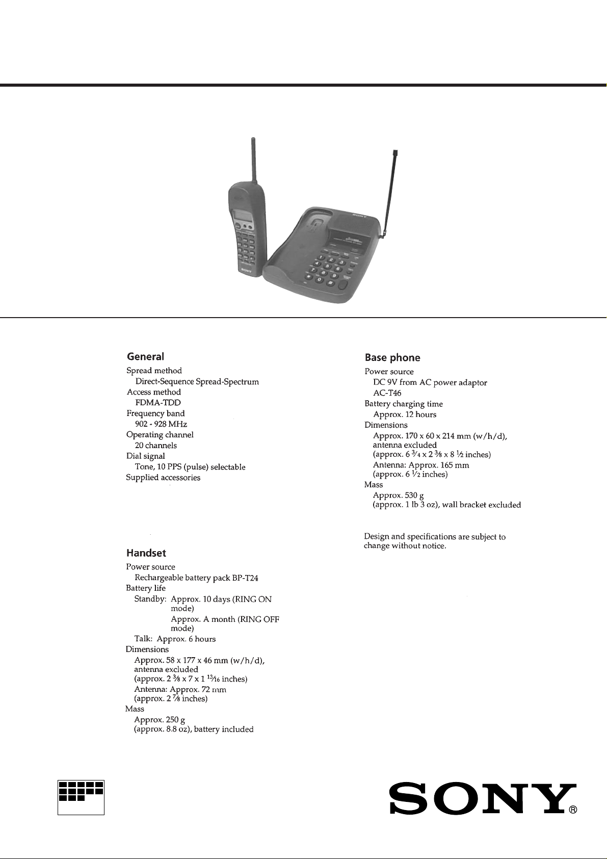
SPECIFICATIONS
E Model
AC power adaptor (AC-T46)
Telephone line cord
Wall bracket/stand for base phone
Rechargeable battery pack (BP-T24)
Directories
CORDLESS TELEPHONE
MICROFILM
Page 2

TABLE OF CONTENTS
1. SERVICING NOTES............................................... 3
2. GENERAL
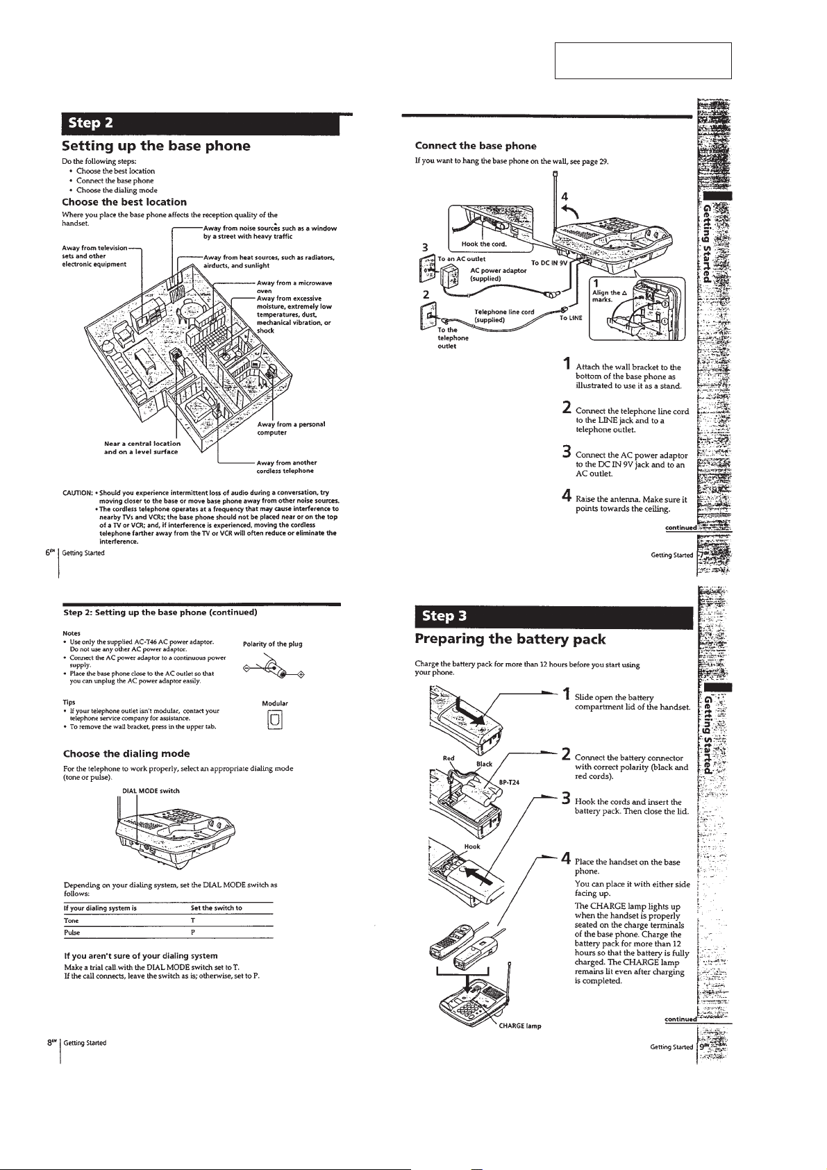
Setting up the base phone ............................................... 4
Preparing the battery pack .............................................. 4
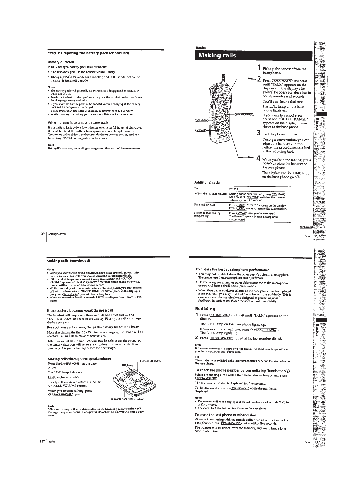
Making calls .................................................................... 5
Receiving calls ................................................................ 6
One-touch dialing............................................................ 6
Speed dialing ................................................................... 7
Phone directory ............................................................... 7
Switching the phones during a call................................. 8
Talking between the phones (Intercom) ......................... 8
Voice paging .................................................................... 9
Transferring a call ........................................................... 9
3. DISASSEMBLY ......................................................... 10
4. 900 MHz SYSTEM OPERATION
4-1. Access Method ................................................................ 13
4-2. Protocol ........................................................................... 13
5. TEST MODE
5-1. Base Unit Section............................................................ 16
5-2. Handset Section............................................................... 17
5-3. RF Testing ....................................................................... 18
Notes on chip component replacement
• Never reuse a disconnected chip component.
• Notice that the minus side of a tantalum capacitor may be damaged by heat.
SAFETY-RELATED COMPONENT WARNING!!
COMPONENTS IDENTIFIED BY MARK ! OR DOTTED
LINE WITH MARK ! ON THE SCHEMATIC DIAGRAMS
AND IN THE PARTS LIST ARE CRITICAL TO SAFE
OPERATION. REPLACE THESE COMPONENTS WITH
SONY PARTS WHOSE PART NUMBERS APPEAR AS
SHOWN IN THIS MANU AL OR IN SUPPLEMENTS PUBLISHED BY SONY.
6. ELECTRICAL ADJUSTMENTS
6-1. Base Unit Section............................................................ 20
6-2. Handset Section............................................................... 21
7. DIAGRAMS
7-1. Block Diagram – BASE UNIT Section –....................... 25
7-2. Block Diagram – HANDSET Section – ......................... 27
7-3. Notes for Printed Wiring Boards
and Schematic Diagrams ................................................ 29
7-4. Printed Wiring Board
– BASE MAIN Board (Side A)/
BASE MICROPHONE Board – ..................................... 31
7-5. Printed Wiring Board
– BASE MAIN Board (Side B) – ................................... 33
7-6. Schematic Diagram – BASE MAIN Section (1/3) – ...... 35
7-7. Schematic Diagram – BASE MAIN Section (2/3) – ...... 37
7-8. Schematic Diagram – BASE MAIN Section (3/3) – ...... 39
7-9. Printed Wiring Board – BASE KEY Section – ............. 41
7-10. Schematic Diagram – BASE KEY Section – ................ 42
7-11. Printed Wiring Board – HAND MAIN Section – ......... 43
7-12. Schematic Diagram – HAND MAIN Section – ............ 45
7-13. IC Pin Function Description ........................................... 48
8. EXPLODED VIEWS ................................................ 53
9. ELECTRICAL PARTS LIST ............................... 55
– 2 –
Page 3
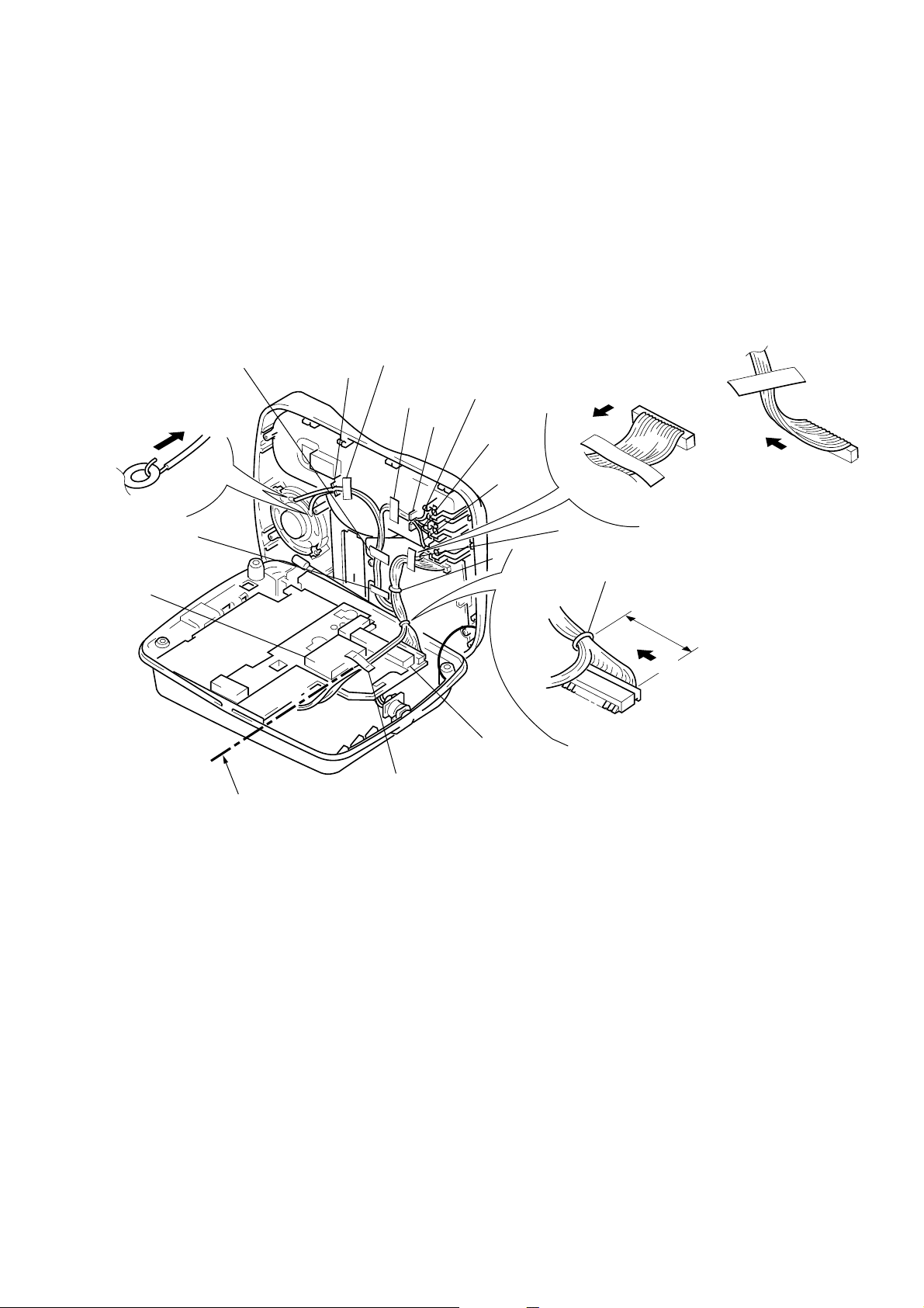
SECTION 1
SERVICING NOTES
CABLE FASTENING METHOD
• TDD noise may be generated in the intercom or handset speech
depending on how the cables are fastened, and therefore fasten
the cables as shown below.
1 Erect the cabinet (upper) 90 degrees.
2 Insert the wires in the ribs at A and B.
3 Clamp them at C and D.
4 Affix the sponges at E and F positions.
5 Fix the cables with tapes at G to L positions.
Note:Tape over the
diode (D1001).
L
Direction for drawing
speaker lead wires
A
G
H
black
B
Cable fasting direction
red
F
K
Affix position
Bottom flushed
white
D
°
90
E
J
Note:Make sure the wires do not
rise above the shield plate.
I
NG
C
clamp stopper
25~30 mm
Cable fasting direction
Cable fasting direction
OK
– 3 –
Page 4
SECTION 2
GENERAL
This section is extracted from
instruction manual.
– 4 –
Page 5
– 5 –
Page 6
– 6 –
Page 7
– 7 –
Page 8
– 8 –
Page 9
– 9 –
Page 10
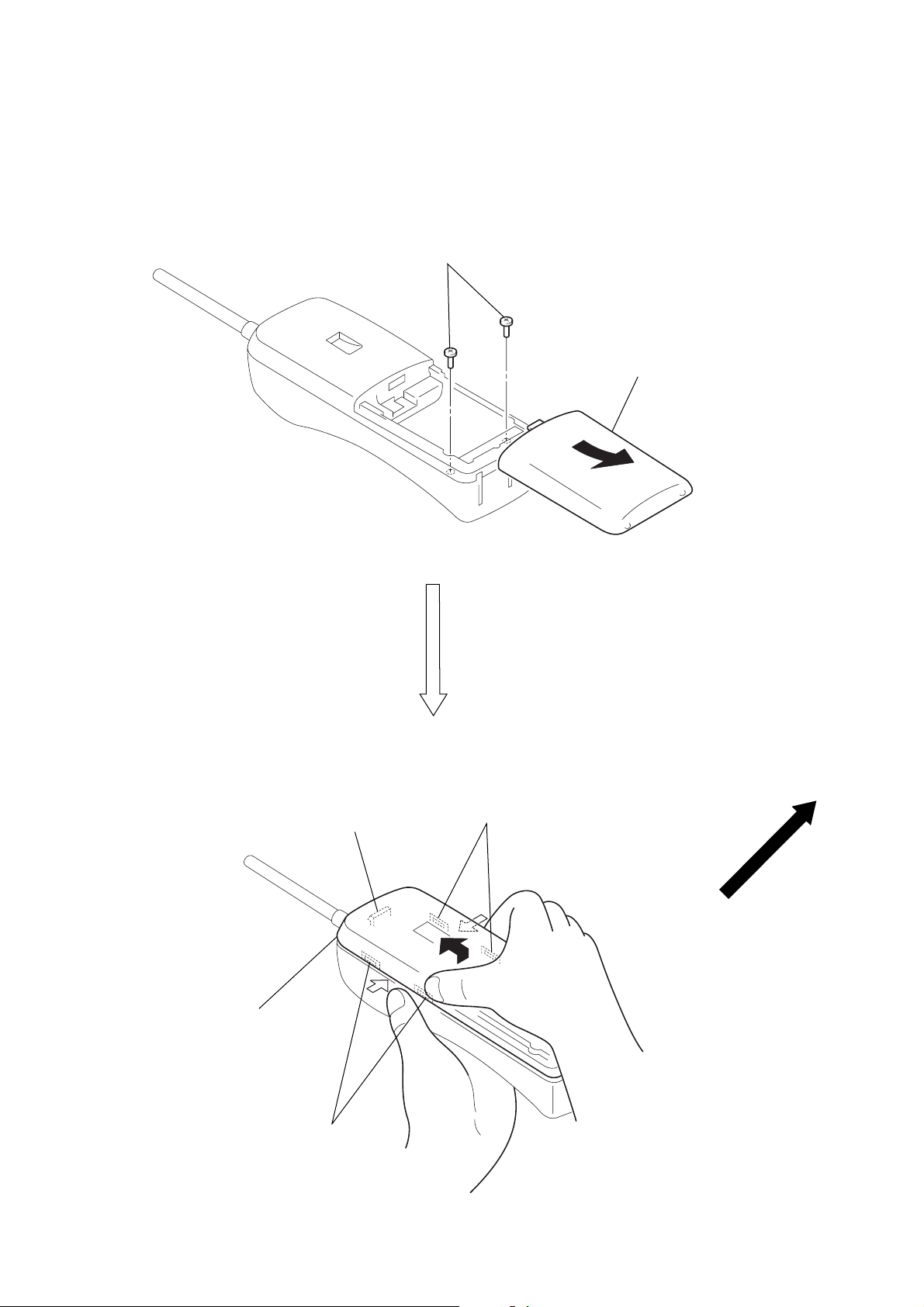
SECTION 3
DISASSEMBLY
Note: Follow the disassembly procedure in the numerical order given.
• HANDSET
REAR CABINET
2
two screws
(BTP 2.6
×
10)
1
Remove the battery case lid
to direction of the arrow
A
A
.
5
Remove the rear cabinet to
direction of the arrow B.
3
two claws
4
claw
B
3
two claws
– 10 –
Page 11
HAND MAIN BOARD
s
)
3
1
connector
screw
(BTP2.6 × 8)
4
Removal of the HAND MAIN
board direction of the arrow A.
(CN401)
A
2
four screws
(P3 × 16)
1
connector
(CN302)
3
three screw
(BTP2.6 × 8
– 11 –
Page 12
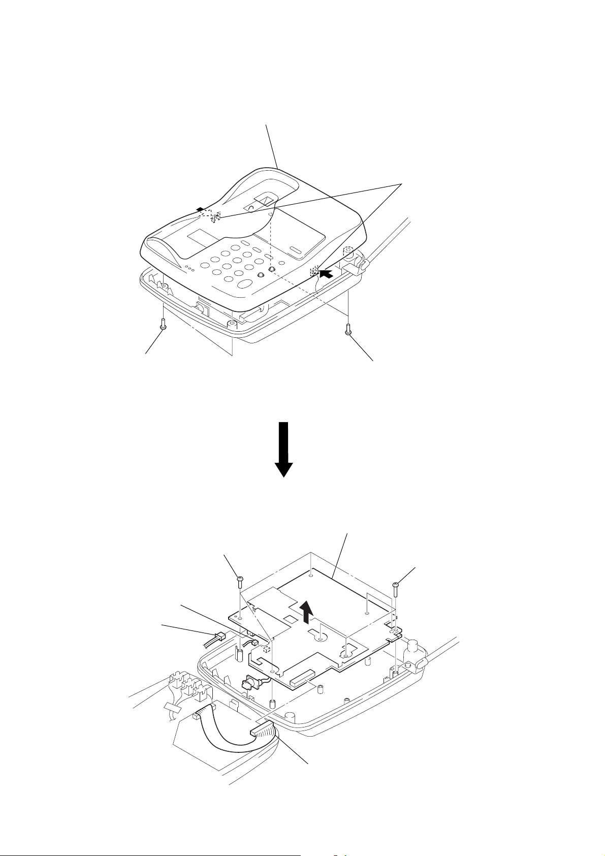
• BASESET
s
BASESET (UPPER) ASS’Y
1
two screws
(P3
×
12)
3
baseset (upper) ass’y
1
two screws
(P3
×
12)
2
two claw
BASE MAIN BOARD
1
connector
(CN601)
1
connector
(CN202)
3
four screws
(BTP2.6 × 8)
2
connector
(CN802)
5
BASE MAIN board
4
four screws
(P3 × 16)
– 12 –
Page 13
SECTION 4
900 MHz SYSTEM OPERATION
4-1. ACCESS METHOD
1. Transfer format & rate
The transfer format & rate of our system is as follows;
Table 4-1. Transfer method
Access method FDMA-TDD
Channel number 20 channel
Channel spacing 1.2 MHz
Modulation method DBPSK
Baseband transfer rate 960 Kbps
Spread method Direct Sequence Spread Spectrum
Chip rate 12 chips/bit
Data transfer rate 80 Kbps
2. Channel Number & Frequencies
RF channels occupy the frequency band 902 – 928 MHz are numbered 1 to 20.
RF channel numbers & center frequencies are specified as follows.
Table 4-2. Channel number & Channel frequency
Channel Channel Center Channel Channel Center
Number Frequency (MHz) Number Frequency (MHz)
1 903.6 11 915.6
2 904.8 12 916.8
3 906.0 13 918.0
4 907.2 14 919.2
5 908.4 15 920.4
6 909.6 16 921.6
7 910.8 17 922.8
8 912.0 18 924.0
9 913.2 19 925.2
10 914.4 20 926.4
4-2. PROTOCOL
1. General
This system realizes the TX/RX superframe by TDD system. The
relation of master/slave dose not decide identification regarding
the protocol between BS and HS, but the initiated side is the master and the requested side is the slave when the RF link has been
established.
2. Initial acquisition
In order to establish the RF link between BS and HS, both of BS
and HS need to have the same system ID. When “power” is applied to this system, the system have to do Initial Acquisition in
order to have the same system ID. It is to exchange a parameter
when the HS is parked on the BS, as soon as the system do System
Parameters Re-initialization.
3. System parameter re-initialization
This System Parameters Re-initialization can realize that the HS
is parked on the BS. So after the BS recognized to be parked the
HS, the BS calculates a system parameter, and then it outputs this
data from the ARTO port, and then the system establishes the RF
link. In order to establish this link, the HS send the A-Frame to the
BS after the HS received the system parameter, and then the BS
send the A-Frame to the HS. The process of System Parameters
Re-initialization is as follows.
Base Station Handset
(PARK)
(Park Detect)(Park Detect)
System Parameters
A-Frame
System ID
confirmed
A-Frame
Fig. 4-1. System Parameters Re-initialization
System ID
confirmed
– 13 –
Page 14
4. Stand-by Mode Operation
(1) HS
When the HS is the stand-by mode (sleep mode), the HS do
the intermittent operation for power save, because the HS is
the battery operation.
This process of stand-by mode operation is as follows.
10 sec
Heart-Beat
10 sec
Heart-Beat Heart-Beat
RX RX RX RX RX
1 sec 1 sec
RX
10 sec
1 sec
2 msec
2 msec 10 msec
10 msec
RXTXRX
Heart-Beat
(Exchange A-Frame for Link confirmation purpose)
Fig. 4-2. Stand-by mode operation (HS)
(2) BS
The BS is supplied the power by AC line. While the BS is the
stand-by, the BS is always a wake state. While the BS monitors the current channel, the BS monitors also the other channel at the same time
Because if the current channel can not use by some interference, the system needs the clear channel information as a part
of system parameter for a channel hop.
If the BS can not receive the A-Frame of Heart-beat from the
HS, it become “link error”, and the system become error recovery mode.
RX
– 14 –
Page 15

5. Link Establishment
Master TX
Master RX
Slave RX
Slave TX
Master
Time Slot
Trip Delay
TX RX TX RX TX
AV
A' V
V
V
VA
VA'
V
According to the following Fig. 4-1, the requested side for link
establishment is the master.
The system have to exchange the A-Frame for link establishment,
and each system ID should be the same ID, and then the system
link is established.
The protocol and timing chart of link establishment are as follows.
Master Slave
A-Frame
System ID
confirmed
A-Frame
V-Frame
V-Frame
V-Frame
V-Frame
Fig. 4-3. Link Establishment protocol
System ID
confirmed
Fig. 4-4. Link Establishment Timing Chart
6. State Change/Termination
After the RF link between HS and BS was established, a movement of each state (State: ON-Hook, OFF-Hook, P A GE, InterCom,
etc) is sent through supervisory bits.
7. Error Recovery
In case of the following situation, The system becomes “Error
Recovery Mode”.
(1) The system failed to move to “Heart-Beat” during “Stand-by
mode, or failed “link establishment”.
(2) The system failed to keep the link.
– 15 –
Page 16

SECTION 5
TEST MODE
5-1. BASE UNIT SECTION
[Start-up]
1. Set the [DIALMODE] switch to the P (PULSE) side.
2. Keeping the [INTERCOM] button pressed, turn the power on.
3. After a start-up acknowledge tone sounds, set the [DIALMODE]
switch from P (PULSE) to T (TONE) side, then return to the P
(PULSE) side.
4. Release the[INTERCOM] button, and the T est Mode will start.
5. Allow for normal ringer to sound at high level f or duration of
500 msec after start-up, then close the line and dial Pause → 0
(DP) → (mode change) → 1 (tone) → 4 (tone) → 8 (tone)
→ # (tone).
6. After dialing, the base unit will go in Test Mode Idle status.
[Ring Detection Test]
1. The LINE LED blinks in synchronization with the RING sgnal
and at the same time, Normal Ringer sounds, if the RING signal is detected in the Test Mode Idle status.
[Charge Detection • ARTO Output Test]
1. Square-wave signal (2.4 kHz) is output to the IC751 pin #¢
(ARTO ter minal) when the CHARGE signal is detected (IC751
pin ^™ (PARKP terminal) H → L) in the Test Mode Idle status.
2. At this time, the EEPROM (IC951) is reset.
[Charge Control Test]
1. IC751 pin *¶ (CHG-HIGH RA TE terminal) outputs H → L →
H once, if IC751 pin *£ (VCHG-MON terminal) changes to H
→ L → H when the CHARGE signal is detected in the Test
Mode Idle status.
[Test Mode by Manual Input]
• T he key input in the Test Mode Idle status can change the set
status to the following modes. However, the transition to another mode within respective test mode groups (A-J) is possible
directly, but in case of transition to other test mode group, the
set must be returned to the T est Mode Idle status once by enter ing the command “0-1-#”.
A) Test mode termination
Command Mode/Operation
0-0-# Terminate the Test mode.
B) Return test mode idle
Command Mode/Operation
0-1-# Return to Test Mode Idle status.
C) Continuous receiving test group (Note 1)
Command Mode/Operation
1-1-# CH1 continuous receiving status (LNA, AGC ON)
D) Continuous transmission test group (Note 1)
Command Mode/Operation
2-1-# CH1 continuous transmission status (TX Power High)
2-2-# CH1 continuous transmission status (TX Power Mid)
2-3-# CH1 continuous transmission status (TX Power Low)
Note 1: Each time the [*] key is pressed, the channels change over as
follows:
CH1 → CH2 → CH3 → … → CH20
E) Loopback test group 1
Command Mode/Operation
3-1-# CODEC Forward Loopback (L1)
(Speech path: Talk status)
(LINE IN → LINE OUT: CODEC LINE IN→
SPKR OUT)
3-2-# ADPCM Forward Loopback (L2)
(Speech path: Talk status)
(LINE IN → CODEC → ADPCM → CODEC →
LINE OUT)
3-3-# ADPCM → RF Loopback
(Speech path: Talk status)
(LINE IN → CODEC → ADPCM → RF → ADPCM
→ CODEC → LINE OUT)
F) TDD test group 1
Command Mode/Operation
4-1-# CH1 TDD mode (Master timing, Power High) status
4-2-# CH1 TDD mode (Master timing, Power Mid) status
4-3-# CH1 TDD mode (Master timing, Power Low) status
4-4-# TDD mode (Slave timing, Standby) status. Power
(Note 2) control
Note 2: To make a speech with the handset, first operate the set in Slave
mode by “4-4-#” command, and operate the counterpart in the
Master mode by “6-1-#” command. However, the ID must be
same. To set the same ID, perform ON-Charge in advance, or
clear the EEPROM by “7-1-#” command. In this case, howe v er,
the speech path should be the intercom status.
G) MMI test group
Command Mode/Operation
5-1-# Key test.
• Press the keys successively in the following
order:
[PGM] → [SPEEDDIAL] → [REDIAL/PAUSE]
→ [FLASH] → [1] → [2] → [3] → [4] → [5]
→ [6] → [7] → [8] → [9] → [*] → [0] →
[#] →[INTERCOM] →[HOLD] →
[SPEAKERPHONE]
• If key input sequence is correct: An acknowledge tone sounds, and the set returns to the T est
Mode Idle status.
• If key input sequence is wrong: An error tone
sounds, and the set returns to the Test Mode
Idle status.
5-4-# LED test.
[LINE] LED lights up when the LED test mode is
selected.
H) TDD test group 2
Command Mode/Operation
6-1-# TDD mode (Master timing) status. Power control.
Refer to the description of “4-4-#” command.
I) Memory clear test group
Command Mode/Operation
7-1-# The contents of EEPROM are cleared. In case of
successful clear, an acknowledge tone sounds.
– 16 –
Page 17

J) Loopback test group 2
Command Mode/Operation
8-1-# ADPCM Forward Loopback
(Speech path: Intercom status)
(MIC IN → SPEAKER OUT: CODEC MIC IN →
ADPCM → CODEC LINE OUT
(Speech path: Intercom status)
5-2. HANDSET SECTION
[Start-up]
1. With the power supplied, press
taneously, and the Test Mode will start.
2. Allow for normal ringer to sound at high level for duration of
500 msec after start-up, then the handset will go in Test Mode
Idle status.
3. The RF in Talk/Intercom status is as follows.
[Test Mode by Manual Input]
• The key input in the Test Mode Idle status can change the set
status to the following modes. However, the transition to another mode within respective test mode groups (A-J) is possible
directly, but in case of transition to other test mode group, the
set must be returned to the Test Mode Idle status once by entering the command “0-1-#”.
A) Test mode termination
Command Mode/Operation
0-0-# The Test mode terminates. The contents of EEPROM
are cleared. In case of successful clear, an
acknowledge tone sounds.
B) Return test mode idle
Command Mode/Operation
0-1-# Return to Test Mode Idle status.
C) Continuous receiving test group (Note 1)
Command Mode/Operation
1-1-# CH1 continuous receiving status (LNA, AGC ON)
D) Continuous transmission test group (Note 1)
Command Description
2-1-# CH1 continuous transmission status (TX Power High)
2-2-# CH1 continuous transmission status (TX Power Mid)
2-3-# CH1 continuous transmission status (TX Power Low)
[TALK], [0], and [1] keys simul-
F) TDD test group 1
Command Mode/Operation
4-1-# CH1 TDD mode (Master timing, Power High) status
4-2-# CH1 TDD mode (Master timing, Power Mid) status
4-3-# CH1 TDD mode (Master timing, Power Low) status
4-4-# TDD mode (Slave timing, Standby) status. Power
control
G) MMI test group
Command Mode/Operation
5-1-# Key test.
• Press the keys successively in the following order:
[TALK,FLASH] → [OFF] → [HOLD] → [VOL/PGM]
→ [INTERCOM] → [REDIAL/PAUSE] → [1] → [2]
→ [3] → [4] → [5] → [6] → [7] → [8] → [9] →
[*] → [0] → [#] → [A] → [B] → [C]
• If key input sequence is correct: An acknowledge
tone sounds, and the set returns to the Test Mode
Idle status.
• If key input sequence is wrong: An error tone
sounds, and the set returns to the Test Mode Idle
status.
5-2-# JOG shuttle test. (Note 2)
5-3-# LCD test.
All dots on LCD lights up immediately when the LCD
test mode is selected.
Note 2: JOG shuttle test
The JOG shuttle test mode makes a check with the LCD display
when JOG shuttle is rotated clockwise or counterclockwise, or
the button is pressed.
JOG shuttle LCD display
Rotate clockwise “R” is displayed at 1st digit on 1st line
Rotate counterclockwise “L” is displayed at 1st digit on 1st line
Press button “P” is displayed at 1st digit on 1st line
H) TDD test group 2
Command Mode/Operation
6-1-# TDD mode (Master timing) status.
I) Memory clear test group
Command Mode/Operation
7-1-# The contents of EEPROM are cleared. In case of
successful clear, an acknowledge tone sounds.
Note 1: Each time the [*] key is pressed, the channels change over as
follows:
CH1 → CH2 → CH3 → … → CH20
E) Loopback test group 1
Command Mode/Operation
3-1-# CODEC Forward Loopback (L1)
(MIC → SP) (within CODEC)
3-2-# ADPCM Forward Loopback (L2)
(MIC → CODEC → ADPCM → CODEC → SP)
3-3-# ADPCM → RF Loopback
(MIC → CODEC → ADPCM → RF → ADPCM →
CODEC → SP)
J) Battery save mode
Command Mode/Operation
9-0-# Battery Save mode.
– 17 –
Page 18

5-3. RF TESTING
This test is for checking the RF system without disassembling the
set in servicing. Perform measurement using the spectrum analyzer and jig antenna.
• T ransmission Wave:
ATTEN 10 dB
RL 0 dBm 10 dB/
MKR –16.00 dBm
903.392 MHz
5-3-1. RF Testing method
Please follow the below instruction to perform RF test.
[Setting Condition]
Connect a receiving antenna to RF INPUT of Spectrum analyzer
and set the unit 10 cm (4 inches) away from the receiving antenna.
Measuring tool: Spectrum analyzer (equivalent to HP8595E)
Jig: Receiving antenna (for Spectrum analyzer)
10 cm
Spectrum
analyzer
Jig antenna
(Utilize the antenna for handset)
10 cm
MKR
903.392 MHz
–16.00 dBm
CENTER 903.600 MHz
RBW 30 kHz
XdB
–7
–8
–9
VBW 30 kHz
–3
–4
–5
–6
Fig. 1
–1
–2
f
SPAN 5.000 MHz
SWP 50.0 msec
5
3
1
2
0
6
4
7
8
9
Spectrum
analyzer
[Check the Transmission Wave]
Purpose
It is necessary to check spectrum wave of transmission wa ve which
is an important factor in order to confirm operational performance
of Spread Spectrum models. If this wave deviates from correct
wave form, normal data transmission cannot be made and, as a
result of that, possibility that occurrence of mute increases and
communication distance becomes shorter will increase.
Measuring process
• Setting Spectrum analyzer:
Center frequency : 903.6 MHz (CH1)
RBW :30 kHz
VBW :30 kHz
Span :3 MHz (or 5MHz)
• Setting Test mode:
Continuous Transmit mode (CH1 High Power)
(Refer to “Test Mode” on page 16)
• Measurement:
Measure transmitting wave.
• Specifications:
Acceptable level [XdB] difference between the highest peak and
the lowest peak of odd side band (the first to seventh side band
from Center Frequency ; Transmission Frequency f0: CH1) is
under 10 dB. (Refer Fig. 1 and Fig. 2)
If output wave form deteriorates, side band appears like Fig. 3
and Fig. 4.
ATTEN 10 dB
RL 0 dBm 10 dB/
MKR
903.233 MHz
–14.67 dBm
CENTER 903.600 MHz
RBW 30 kHz
VBW 30 kHz
f–1f
Fig. 2
Fig. 3
1
MKR –14.67 dBm
903.233 MHz
SPAN 5.000 MHz
SWP 50.0 msec
– 18 –
Page 19

18dB
• Measurement:
Measure peak level by Spectrum analyzer.
–5
–6
–7
–8
–9
–1
–4
–3
–2
3
4
5
7
1
2
6
8
9
PEAK
LOG
10
dB/
WA SB
SC FC
CORR
PLOTTER ADRS
0
903.587 MHzMKR
–3.67 dBmAT 10 dB.0 dBmREF
Fig. 4
[Check Center Frequency]
Measuring process
• Setting Spectrum analyzer:
Center frequency : 903.6 MHz (CH1)
RBW : 10 kHz
VBW : 10 kHz
Span : 1 MHz
• Setting Test mode:
Continuous Transmit mode (CH1 High Power)
(Refer to “Test Mode” on page 16)
• Measurement:
Measure transmitting wave f0 (Formula of center frequency)
(Refer Fig.5)
• Specification:
903.6 MHz ± 27 kHz
• Center Frequency:
10dB/
f
f
f
–2
1
–1
f
0
f
2
Tr-A
CENTER 903.600 MHz
RES BW 1.0 MHz
VBW 100 kHz
SPAN 5.000 MHz
SWP 20.0 msec
DATA (UNIT; dbm)
NO HANDSET BASESET
HIGH MID LOW HIGH MID LOW
1 –3.93 –20.95 -34.53 –2.36 –19.17 –32.81
2 –3.70 –20.36 –33.75 –1.52 –18.33 –30.79
3 –4.47 –21.48 –34.78 –4.36 –18.65 –33.3
4 –4.64 –21.85 –35.12 –4.25 –19.37 –33.05
5 –4.52 –21.18 –35.54 –2.35 –19.05 –32.95
6 –4.02 –21.57 –35.12 –2.96 –19.14 –33.45
7 –5.03 –22.14 –35.45 –4.12 –19.12 –33.01
8 –5.58 –22.35 –35.61 –2.89 –18.56 –32.12
9 –4.03 –21.32 –35.82 –5.01 –18.33 –32.41
10 –4.43 –19.69 –33.92 –2.74 –17.28 –31.33
× –4.435 –21.29 –34.96 –3.256 –18.7 –32.52
σ 0.5336 0.7634 0.6747 1.0562 0.5895 0.8273
× + 4σ –2.301 –18.24 –32.27 0.9687 –16.34 –29.21
× – 4σ –6.569 –24.34 –37.66 –7.481 –21.06 –35.83
PN
• Specification:
HANDSET MIN –17 dBm
(at High power: Include location loss)
BASE SET MIN –18 dBm
(at High power: Include location loss)
Fig. 5
[Confirm Transmitting output]
Measuring process
• Setting Spectrum analyzer:
Center frequency : 903.6 MHz (CH1)
RBW : 1 MHz
VBW : 100 kHz
Span : 5 MHz
• Setting Test mode:
Continuous Transmit mode (CH1 High Power)
(Refer to “Test Mode” on page 16)
– 19 –
Page 20

SECTION 6
P
N
L
L
L
ELECTRICAL ADJUSTMENTS
6-1. BASE UNIT SECTION
• Make the set in Test mode (see page 16)
1. Checking RX I & Q Output Level
Setting:
oscilloscope
+
–
SSG
Procedure:
1. Place the base unit in the Continuous Receive mode (CH1,
LNA ON, AGC ON).
2. Set the SSG frequency to the frequency on CH1 + 300 kHz,
and the RF output level to –95 dBm.
3. Measure the output level of RXIN, RXIP, RXQN and RXQP
with a level meter. At this time, confirm with an oscilloscope
that a sine wave of 300 kHz is output.
4. Confirm that the measured output level is –31.0 to –24.0
(TYPICAL –27.0) dBV. If IC951 was replaced (there is no ID
data), the output level is –31.0 to –24.0 dBV.
5. Also, execute steps 1 through 4 for the channels 10 and 20.
level meter
+
–
TP906: RXIP
TP905: RXIN
TP904: RXQ
TP903: RXQ
TP919: GND
ANTENNA TERMINA
3. Checking TX Output
Setting:
peak power meter
+
–
ANTENNA TERMINA
Procedure:
1. Place the base unit in the Continuous Transmit mode (CH1,
High power).
2. Measure the ANT OUT output of the RF module in the base
unit using a peak power meter.
3. Confirm that the measured output is 80 mW (MIN 30 mW).
4. Also, execute steps 1 through 4 for the channels 10 and 20.
CH10: 80 mW (MIN 30 mW)
CH20: 75 mW (MIN 25 mW)
* For the frequency on each channel, see page 13.
2. Checking TX Center Frequency
Setting :
• short: TP918 ↔ TP919
frequency counter
+
–
Procedure:
1. Short TP918 and TP919 (GND) on the B ASE MAIN board in
the base unit.
2. Place the base unit in the Continuous Transmit mode (CH1,
High power).
3. Measure the ANT OUT frequency of the RF module in the
base unit using a frequency counter.
4. Confirm that the measured frequency is 903.600 MHz ±
27 kHz.
5. Also, execute steps 1 through 4 for the channels 10 and 20.
ANTENNA TERMINA
– 20 –
Page 21

6-2. HANDSET SECTION
P
N
L
L
L
• Make the set in Test mode (see page 17)
1. Checking RX I & Q Output Level
Setting:
oscilloscope
+
–
SSG
Procedure:
1. Place the handset in the Continuous Receive mode (CH1, LNA,
AGC ON).
2. Set the SSG frequency to the frequency on CH1 + 300 kHz,
and the RF output level to –95 dBm.
3. Measure the output level of RXIN, RXIP, RXQN, and RXQP
with a level meter. At this time, confirm with an oscilloscope
that a sine wave of 300 kHz is output.
4. Confirm that the measured output level is –31.0 to –24.0 (TYPICAL –27.0) dBV. If IC502 was replaced (there is no ID data),
the output level is –31.0 to –24.0 dBV.
5. Also, execute steps 1 through 4 for the channels 10 and 20.
level meter
+
–
TP520: RXIP
TP521: RXIN
TP522: RXQ
TP523: RXQ
TP553: GND
ANTENNA TERMINA
3. Checking TX output
Setting:
peak power meter
+
–
ANTENNA TERMINA
Procedure:
1. Place the handset in the Continuous Transmit mode (CH1, High
power).
2. Measure the ANT OUT output of the RF module in the handset using a peak power meter.
3. Confirm that the measured output is 80 mW (MIN 20 mW).
4. Also, execute steps 1 through 3 for the channels 10 and 20.
CH10: 80 mW (MIN 20 mW)
CH20: 50 mW (MIN 10 mW)
* For the frequency on each channel, see page 13.
2. Checking TX Center Frequency
Setting:
• short: TP555 ↔ TP553
frequency counter
+
–
ANTENNA TERMINA
Procedure:
1. Short TP555 and TP553 (GND) on the HAND MAIN board in
the handset.
2. Place the handset in the Continuous Transmit mode (CH1, High
power).
3. Measure the ANT OUT frequency of the RF module in the handset using a frequency counter .
4. Confirm that the measured frequency is 903.600 MHz ±
27 kHz.
5. Also, execute steps 1 through 4 for the channels 10 and 20.
– 21 –
Page 22

Adjustment Location:
l
y
[BASE MAIN board]
(Side B)
SW951
T ˜ P
1
ANTENNA TERMINAL
SSG : Checking RX I & Q Output leve
frequency counter : Checking TX Center Frequenc
peak power meter : Checking TX Output
TP918 and TP919 short :
Checking TX Center Frequency
level meter :
Checking RX I & Q Output Level
TP919: GND
TP918: TEST
TP903: RXQN
TP904: RXQP
TP905: RXIN
TP906: RXIP
CN902
16
1
CN901
8
RFU901
RF UNIT
– 22 –
Page 23

l
y
[HAND MAIN board]
(Side A )
1
ANTENNA TERMINAL
SSG : Checking RX I & Q Output leve
frequency counter : Checking TX Center Frequenc
peak power meter : Checking TX Output
16
1
8
CN501
S502
CN502
RFU501
RF UNIT
TP553: GND
TP555: TEST
TP523: RXQN
TP522: RXQP
TP521: RXIN
TP520: RXIP
TP555 and TP553 short :
Checking TX Center Frequency
level meter :
Checking RX I & Q Output Level
– 23 –
Page 24

SECTION 7
DIAGRAMS
7-1. BLOCK DIAGRAM – BASE UNIT Section –
SPP-SS964
ANT901
TELESCOPIC
ANTENNA
RFU901
RF UNIT
VBAT (FOR RX)
LNAATN
VBAT (FOR TX)
VBAT (FOR PLL)
TX.DATA
TXPWR0
TXPWR1
TXRXSW
SYNDATA
SYNCLK
SYNSTB
REFOSC
• SIGNAL PATH
: RX
: TX
: RX (INTERCOM)
: TX (INTERCOM)
: BELL
05
RXIP
RXIN
RXQP
RXQN
RXEN
AGC
TXEN
SYNEN
CN901
1
6
5
4
3
8
7
2
CN902
2
10
7
4
5
6
3
12
11
13
15
14
SW951-2
DIAL MODE
SW952
RINGER
B+
B+
Q751
Q750, 751
TX POWER
ATTENUATOR
D1002
LINE
T
P
OFF
ON
Q750
B+
9.6MHz
B+
B+
X752
RXIP
51
RXIN
52
RXQP
53
RXQN
54
LNAATN
43
RXEN
44
AGC
60
TXDATA
49
TXPWR0
85
TXPWR1
80
TXEN
79
TXRXSEL
82
SYNDATA
65
SYNCLK
71
SYNSTB
72
SYNEN
75
SYNTH5MCLK
66
LINE-LED
68
DIALMODE
88
RING MODE ON/OFF
21
XTALI
97
XTALO
98
ASIC
IC751
CDCDATAO
CDCFRAME
CDCICLK
CDCMCLK
CDCDATAI
AFC (BEEP)
DIALMUT
INTC & HOLD
KEY MATRIX
S1001 – 1019
RESETO
CTRL
CODEC
IC701
DATAI
25
32
28
26
27
24
59
95
20
KEY-OUT0 – KEY-OUT3KEY-IN0 – KEY-IN5
36, 35, 31, 2210 – 15
29
20
21
26
25
30
T
P
SW951-1
DIAL MODE
Q212, 213
FRAME
ICLK
MCLK
RESETB
DATAO
AF AMP
REGISTER
REGISTER
NVDI
76 77
5 6
SDA
EEPROM
IC951
16 BIT
CONTROL
REGISTER
16 BIT
DIAL MUTE
SWITCH
Q214
26
23
NVDO
SCL
MODULATOR &
FILTER
MODULATOR &
FILTER
DTMF MUTE
SWITCH
RLI1
TLI1
HYBRID
RESETI
96
Q215
ATTENUATOR
CONTROL CIRCUIT
LEVEL DETECTOR
AMP
HTIHTO–
RESET SIGNAL
GENERATOR
IC602
SW601
RESET
+
21
76
SPEAKER
RXI
DIAL TONE
DETECTOR
LINEO
LINE
AMP
SPKPO
SPKMO
AMP
LINE-IN
LINE
AMP
MICIN
MIC
AMP
B.P.F.
RX
ATTENUATOR
VOICE SPEAKERPHONE
IC103
TXO
ATTENUATOR
B+
17
19
18
13
11
TX
34
ARTO
B.P.F.
MUTE SWITCH
B.P.F.
B.P.F.
RXO
VLC
RLI2
TLI2
TXI
D1001
CHARGE
INTERCOM
Q216
22
13
20
17
98
+
SPEAKER
VOLUME
MCO
10
PARKP
62 87
+
RV201
CD
3
AF AMP
Q203, 204
+
INTERCOM
MUTE SWITCH
Q217
MCI
MIC
AMP
MUT
12
86 92
SPKEN
CHG-HIGH RATE
QUICK/NORMAL
CHARGE CONTROL
Q601, 655
DIAL MUTE
Q210
11
TEL AMP
Q201, 202
AF AMP
Q208, 209
VIN
4
POWER AMP
IC104
MIC501
MIC
AUDIO SYSTEM B+
DIGITAL SYSTEM B+
CHARGE DETECT
CD
1
SP-MUT
VO1
VO2
Q653
TRANSFORMER
+
PROTECT
OFF HOOK MUTE
SWITCH
Q211
5
8
+5V
REGULATOR
IC603
+5V
REGULATOR
IC601
T101
LINE
Q101
LEVEL SHIFT
SP101
(SPEAKER)
Q852
BRANCH DETECT
PH102,
Q102, 103
94
BRANCH-DET
CHARGE
CONTROL
Q651, 652, 654
D105 – 108
HOOK ON/OFF
PH103
HOOK ON/OFF
CONTROL
Q207
37
OFFHOOK
ART
MJ101
LINE
RINGER
DETECT
PH101
BUFFER
Q206
81
RINGIN
J601
+
–
DC IN 9V
+
–
CHARGE
TERMINAL
– 25 – – 26 –
Page 25

SPP-SS964
7-2. BLOCK DIAGRAM – HANDSET Section –
ANT501
(ANTENNA)
RFU501
RF UNIT
VBAT (FOR RX)
RXIP
RXIN
RXQP
RXQN
LNAATN
RXEN
AGC
VBAT (FOR TX)
VBAT (FOR PLL)
TX.DATA
TXPWR0
TXPWR1
TXEN
TXRXSW
SYNDATA
SYNCLK
SYNSTB
SYNEN
REFOSC
1
6
5
4
3
8
7
2
2
10
7
4
5
6
3
12
11
13
15
14
CN501
CN502
B+
B+
Q504
Q504, 505
TX POWER
ATTENUATOR
Q505
RXIP
51
RXIN
52
RXQP
53
RXQN
54
LNAATN
43
RXEN
44
AGC
60
TXDATA
49
TXPWR0
85
TXPWR1
80
TXEN
79
TXRXSEL
82
SYNDATA
65
SYNCLK
71
SYNSTB
72
SYNEN
75
SYNTH5MCLK
66
ASIC
IC501
CDCDATAO
CDCFRAME
CDCICLK
CDCMCLK
RESETO
CDCDATAI
NVDI
NVDO
CODEC
IC401
LINE
AMP
LINEO
17
BUZZER DRIVE
Q502
BZ401
(BUZZER)
• SIGNAL PATH
: RX
: TX
: BELL
DATAI
25
32
28
26
27
24
76
77
29
20
21
26
25
30
5
6
FRAME
ICLK
MCLK
RESETB
DATAO
SKDI
DO
EEPROM
IC502
16 BIT
REGISTER
CONTROL
REGISTER
16 BIT
REGISTER
MODULATOR &
FILTER
MODULATOR &
FILTER
10 – 15
KEYPADI0 – KEYPADI5
KEY MATRIX
SW1 – 20, S502
KEYPADB0 – KEYPADB3
SPEAKER
AMP
LINE
AMP
MIC
AMP
36, 35, 31, 22
SPKPO
SPKMO
LINE-IN
MICIN
19
18
13
11
MIC AMP
Q1
SW601
(JOG)
LIQUID CRYSTAL DISPLAY UNIT
69 70 39
JOG (A)
JOG (B)
6 – 9
D4 – D7
MIC401
(MIC)
SP401
(SPEAKER)
LCD501
78 67
LCDRW
LCDRS
LCDCS
B+ SWITCH
Q501
92
LCDPWRP
B+
XTALO
XTALI
97 98
X501
9.6MHz
S501
RING
05
RINGOFF
83
B+
OFF
ON
RESETI
96
RESET SWITCH
Q302, 303
RESET SIGNAL
GENERATOR
IC301
B+
PARKP
62
RECHARGEABLE
BATTERY
(BP-T24)
CHARGE ON
DETECT
Q301
ARTI
33
D301 – 304
LEVEL SHIFT
Q503
D305
ART
CHARGE
+
TERMINAL
–
– 27 –
– 28 –
Page 26

SPP-SS964
4 Vp-p
104 ns
7-3. NOTES FOR PRINTED WIRING BOARDS
AND SCHEMATIC DIAGRAMS
Note on Printed Wiring Board:
• X : parts extracted from the component side.
• Y : parts extracted from the conductor side.
• p : parts mounted on the conductor side.
• b : Pattern from the side which enables seeing.
Caution:
Pattern face side: Parts on the pattern f ace side seen from
(Side B) the pattern face are indicated.
Parts face side: Parts on the parts face side seen from
(Side A) the parts face are indicated.
• Indication of transistor.
C
Q
B
E
These are omitted.
Note on Schematic Diagram:
• All capacitors are in µF unless otherwise noted. pF: µµF
50 WV or less are not indicated except for electrolytics
and tantalums.
• All resistors are in Ω and 1/
specified.
• C : panel designation.
Note: The components identified by mark ! or dotted line
with mark ! are critical for safety.
Replace only with part number specified.
• U : B+ Line.
• Power voltage is dc 9 V and fed with regulated dc power
supply from external power voltage jack (J601 on the
BASE MAIN board).
• Power voltage is dc 12 V and fed with regulated dc power
supply from modular jack (MJ101 on the BASE MAIN
board) with 100 Ω in series.
• Power voltage is dc 3.6 V and fed with regulated dc power
supply from battery terminal (CN301 on the HAND MAIN
board).
• Voltages and wavef orms are dc with respect to ground in
test mode.
• Voltages are taken with a V OM (Input impedance 10 MΩ).
Voltage variations may be noted due to normal production tolerances.
• Waveforms are taken with a oscilloscope.
Voltage variations may be noted due to normal production tolerances.
• Circled numbers refer to waveforms.
• Signal path.
N : RX
F : RX(INTERCOM)
O : TX
e : TX(INTERCOM)
P : bell
4
W or less unless otherwise
• Waveforms
– BASE MAIN Board –
1 IC751 (¶ (XTALI)
– HAND MAIN Board –
1 IC501 (¶ (XTALI)
2.9 Vp-p
104 ns
– 29 –
– 30 –
Page 27

SPP-SS964
7-4. PRINTED WIRING BOARDS – BASE MAIN Board (Side A)/BASE MICROPHONE Board –
• Semiconductor
Location
(SIDE A)
Ref. No. Location
IC602 G-4
IC701 F-2
IC751 D-3
IC951 B-4
Q208 E-9
Q209 F-10
Q210 F-11
Q211 F-10
(Page 33)
– 31 –
(Page
41)
– 32 –
Page 28

7-5. PRINTED WIRING BOARD – BASE MAIN Board (Side B) –
SPP-SS964
• Semiconductor
Location
(SIDE B)
Ref. No. Location
D100 B-6
D102 B-11
D103 A-11
D104 C-11
D105 A-10
D106 A-10
D107 B-10
D108 B-10
D110 C-9
D601 I-9
D602 E-8
D603 I-9
D652 H-9
D653 H-9
D701 F-3
D702 F-3
D703 F-3
D704 H-2
D705 H-2
IC103 K-5
IC104 I-5
IC601 C-6
IC603 F-8
PH101 D-11
PH102 E-8
PH103 C-10
Q101 C-9
Q102 C-10
Q103 B-9
Q201 E-10
Q202 E-9
Q203 F-10
Q204 F-10
Q206 D-11
Q207 D-10
Q212 G-11
Q213 H-11
Q214 G-9
Q215 G-9
Q216 I-10
Q217 D-10
Q601 I-8
Q651 H-8
Q652 H-8
Q653 I-7
Q654 I-9
Q655 I-9
Q750 C-5
Q751 B-4
Q852 H-10
– 33 –
(Page 31)
– 34 –
Page 29

SPP-SS964
7-6. SCHEMATIC DIAGRAM – BASE MAIN Section (1/3) – • See page 30 for Waveform. • See page 47 for IC Block Diagrams.
(Page 42)
(Page 37)
– 35 –
(Page 39)
(Page 39)
– 36 –
Page 30

7-7. SCHEMATIC DIAGRAM – BASE MAIN Section (2/3) – • See page 47 for IC Block Diagrams.
(Page
36)
SPP-SS964
(Page 39)
– 37 –
– 38 –
Page 31

SPP-SS964
7-8. SCHEMATIC DIAGRAM – BASE MAIN Section (3/3) – • See page 47 for IC Block Diagrams.
(Page
36)
(Page 37)
(Page 35)
– 39 –
– 40 –
Page 32

7-9. PRINTED WIRING BOARD – BASE KEY Section – 7-10. SCHEMATIC DIAGRAM – BASE KEY Section –
(Page 35)
SPP-SS964
(Page 31)
– 41 –
Note
• b : Pattern of the side which is seen. (Carbon pattern)
• : Pattern from the side which enables seeing.
– 42 –
Page 33

SPP-SS964
7-11. PRINTED WIRING BOARD – HAND MAIN Section –
• Semiconductor
Location
(SIDE A)
Ref. No. Location
D502 B-3
D503 B-3
Q501 A-3
Q504 C-2
Q505 C-2
• Semiconductor
Location
(SIDE B)
Ref. No. Location
D301 B-11
D302 B-10
D303 A-11
D304 A-10
D305 B-10
D306 A-9
D401 C-12
D402 C-12
D505 B-11
IC301 B-9
IC401 A-6
IC501 C-4
IC502 C-2
Q1 A-11
Q301 B-9
Q302 B-9
Q303 C-8
Q502 C-12
Q503 B-11
Note:
• Y : carbon pattern
– 43 –
– 44 –
Page 34

7-12. SCHEMATIC DIAGRAM – HAND MAIN Section – • See page 30 for Waveform. • See page 47 for IC Block Diagrams.
SPP-SS964
– 45 –
– 46 –
Page 35

• IC Block Diagrams
IC103 MC34118DW (BASE MAIN BOARD)
RLI1
CPR
GND
28
LEVEL
DETECTOR
LEVEL
DETECTOR
FILTER
AMP
1
FO
RLO1
RXO
TLO1
2526 24
3
CD
HYBRID
4
VCC
23
VCC
AMP 2
5
TLI1
22
RX
ATTENUATOR
BACKGROUND
NOISE
DETECTOR
COMPARATOR
AGC
+
–
HTO+
VR
6
HTO–
27
2
FI
HYBRID
AMP 1
RXI
21
DIAL
TONE
DETECTOR
ATTENUATOR
CONTROL BLOCK
VR
+
–
7
HTI
BACKGROUND
DETECTOR
COMPARATOR
8
TXO
IC401 10497-15 (HAND MAIN BOARD)
IC701 10497-15 (BASE MAIN BOARD)
REFCNTL
XCLKONCICLK
FRAM
SPKPO
SPKMO
LINEO
1719 182021222324
RESETB
MCLK
DVSS
DVDD
DATAI
DATAO
25
26
27
28
29
30
31
NC
32
NC
16 BIT
REGISTOR
CONTROL
REGISTOR
16 BIT
REGISTOR
MODULATOR
& FILTER
MODULATOR
& FILTER
2 345 6 7 8
1
NCNCNCNCNC
AGND
VREF
MICBIAS
NOISE
RLI2
RLO2
19
20
TX
ATTENUATOR
9
10
TXI
16
VOXRNT
VOXSND
15
14
AVDD
LINE-IN
13
AVSS
12
11
MICIN
10
RBIAS
9
NC
IC104 MC34119DR2 (BASE MAIN BOARD)
TLO2
18
LEVEL
DETECTOR
LEVEL
DETECTOR
MIC
AMP
MCO
TLI2
CPT
VB
15
17
16
VREF
VR
+
–
14
12
13
11
CT
VLC
MCI
MUT
VO2
GNDVcc
8 7 6 5
BIAS
CIRCUIT
CD
CF 2
IC502 S-24C16AFJ-TB (HAND MAIN BOARD)
IC951 S-24C02AFJ-TB (BASE MAIN BOARD)
VCC
8
START
LOGIC
1
NC
STOP
LOAD
R/W
TEST INPUT
CONTROL
LOGIC
WORD
ADDRESS
COUNTER
OUT
D
ACK
7
START CYCLE
XDEC
INC
5
PIN
2
NC
SCL
6
32
2
CK
3
NC
_
+
CF 1
H.V. GENERATION
TIMING
& CONTROL
2
E PROM
32 x 32
DATA REGISTER
4321
32
YDEC
8
V in
7-13. IC PIN FUNCTION DESCRIPTION
• HAND MAIN BOARD IC501 M7012-11 (ASIC)
Pin No. Pin Name I/O Function
VO1
+
_
SDA
5
OUT
D
4
VSS
1 KEYPADB5 O
2D0I
3, 4 D1, D2 I/O
5D3I
6 to 9 D4 to D7 O
10 to 15
KEYPADI0 to
KEYPADI5
I
16 VSSC —
17 VDDC —
18 VDDP —
19 VSSC —
20 OSCI I
21 OSCO O
22
23
KEYPADB3
KEYPADB4
O
O
24 CDCDATAI I
25 CDCDATAO O
26 CDCMCLK O
27 RESETO O
28 CDCICLK O
29 VDDP —
30 VSSP —
31 KEYPADB2 O
32 CDCFRAME O
33 ARTI I
34 ARTO O
35, 36
KEYPADB1,
KEYPADB0
O
37 GPIOB7 O
38 VDDP —
39 LCDCS O
40 VDDC —
41 VSSC —
42 TEST I
43 LNAATN O
44 RXEN O
45 VDDA —
46 VSSA —
47 VDDA —
48 VSSA —
49 TXDATA O
50 VRP O
51 RXIP I
52 RXIN I
53 RXQP I
54 RXQN I
55 NC —
Key output terminal Not used (open)
Selection input of the model Fixed at “L” in this set
Not used (open)
Selection input of the test mode Not used (open)
Serial data output to the liquid crystal display unit (LCD501)
Key return signal input from the key matrix “L” input when key pressing
Ground terminal (for core)
Power supply terminal (+5V) (for core)
Power supply terminal (+5V) (for pad)
Ground terminal (for core)
Sub system clock input terminal (32.768 kHz) Not used (open)
Sub system clock output terminal (32.768 kHz) Not used (open)
Key send signal output to the key matrix
Key output terminal Not used (open)
Transmit data input from the CODEC (IC401)
Receive data output to the CODEC (IC401)
Master clock signal output to the CODEC (IC401)
Reset signal output to the CODEC (IC401) “L”: reset
Interface clock signal output to the CODEC (IC401)
Power supply terminal (+5V) (for pad)
Ground terminal (for pad)
Key send signal output to the key matrix
Frame output to the CODEC (IC401)
ART input from the base unit
ART output terminal Not used (open)
Key send signal output to the key matrix
Not used (open)
Power supply terminal (+5V) (for pad)
Chip select signal output to the liquid crystal display unit (LCD501) “L” active
Power supply terminal (+5V) (for core)
Ground terminal (for core)
Setting terminal for the test mode “L”: test mode Normally: fixed at “H”
LNA gain selection signal output to the RF unit “H”: low gain
RX system enable signal output to the RF unit “H”: enable
Power supply terminal (+5V) (for analog)
Ground terminal (for analog)
Power supply terminal (+5V) (for analog)
Ground terminal (for analog)
Transmit data output to the RF unit
Analog reference voltage output terminal
Receive data (I positive) input from the RF unit
Receive data (I negative) input from the RF unit
Receive data (Q positive) input from the RF unit
Receive data (Q negative) input from the RF unit
Not used (open)
– 47 –
– 48 –
Page 36

Pin No. Pin Name I/O Function
56 IBIAS I
57 AGND —
58 BATTERY I
59 AFC O
60 AGC O
61 CALLER-ID O
62 PARKP I
63 VDDC —
64 VSSP —
65 SYNDATA O
66 SYNTH5MCLK O
67 LCDRS O
68 LED4 O
69 JOG (A) I
70 JOG (B) I
71 SYNCLK O
72 SYNSTB O
73 VDDP —
74 VSSP —
75 SYNEN O
76 NVDI I/O
77 NVDO O
78 LCDRW O
79 TXEN O
80 TXPWR1 O
81 GPIOB6 O
82 TXRXSEL O
83 RINGOFF I
84 BASEP I
85 TXPWR0 O
86, 87
100 VSSP —
GPIOB5, GPIOB0
88 GPIOA7 O
89 LED1 O
90 VDDC —
91 VSSC —
92 LCDPWRP O
93 SLEEP O
94 GPIOB4 O
95 NVCLK O
96 RESETI I
97 XTALI I
98 XTALO O
99 VDDP —
Analog bias input terminal
Analog ground terminal
Battery voltage detection input terminal
Not used (open)
Auto gain control signal output to the RF unit
Not used (open)
Charge detection input terminal “L”: charge on
Power supply terminal (+5V) (for core)
Ground terminal (for pad)
Synthesizer data output to the RF unit
Synthesizer reference oscillator output to the RF unit (9.62 MHz)
Register selection signal output to the liquid crystal display unit (LCD501)
“L”: instruction register, “H”: data register
LED drive signal output terminal “L”: LED on Not used (open)
Jog dial pulse input of the rotary encoder (SW601) (A phase input)
Jog dial pulse input of the rotary encoder (SW601) (B phase input)
Synthesizer clock signal output to the RF unit
Synthesizer strobe signal output to the RF unit
Power supply terminal (+5V) (for pad)
Ground terminal (for pad)
Synthesizer power control signal output to the RF unit “H”: enable
Two-way data bus with the EEPROM (IC502)
Clock signal output to the EEPROM (IC502)
Data read/write selection signal output to the liquid crystal display unit (LCD501)
“L”: data write, “H”: data read
TX system enable signal output to the RF unit “H”: enable
PA power selection signal output to the RF unit
Not used (open)
TX/RX selection signal output to the RF unit “L”: RX, “H”: TX
RING on/off switch (S501) input terminal “L”: ringer off, “H”: ringer on
Setting terminal for the base/handset selection
“L”: base unit, “H”: handset unit (CMOS receiver with pull-up)
PA power selection signal output to the RF unit
O
Not used (open)
Muting control signal output for the speaker amplifier “H” active Not used (open)
LED drive signal output terminal “L”: LED on Not used (open)
Power supply terminal (+5V) (for core)
Ground terminal (for core)
Power on/off control signal output for the liquid crystal display unit (LCD501)
“L”: power on, “H”: power off
Not used (open)
Not used (open)
Not used (open)
System reset signal input from the reset signal generator (IC301) “L”: reset
For several hundreds msec. after the power supply rises, “L” is input, then it changes to “H”
Main system clock input terminal (9.6 MHz)
Main system clock output terminal (9.6 MHz)
Power supply terminal (+5V) (for pad)
Ground terminal (for pad)
– 49 –
Page 37

• BASE MAIN BOARD IC751 C7311-11 (ASIC)
Pin No. Pin Name I/O Function
1 KEY-OUT5 O
2D0I
3, 4 D1, D2 O
5D3I
6 to 9 D4 to D7 O
10 to 15
16 VSSC —
17 VDDC —
18 VDDP —
19 VSSC —
20
21
22
23
24 CDCDATAI I
25 CDCDATAO O
26 CDCMCLK O
27 RESETO O
28 CDCICLK O
29 VDDP —
30 VSSP —
31 KEY-OUT2 O
32 CDCFRAME O
33 ARTI I
34 ARTO O
35, 36
37 OFFHOOK O
38 VDDP —
39 LCDCS O
40 VDDC —
41 VSSC —
42 TEST I
43 LNAATN O
44 RXEN O
45 VDDA —
46 VSSA —
47 VDDA —
48 VSSA —
49 TXDATA O
50 VRP O
51 RXIP I
52 RXIN I
53 RXQP I
KEY-IN0 to
KEY-IN5
INTC & HOLD
CTRL
RING MODE
ON/OFF
KEY-OUT3
KEY-OUT4
KEY-OUT1,
KEY-OUT0
Key output terminal Not used (open)
Selection input of the model (fixed at “L” in this set)
Not used (open)
Not used (open)
Not used (open)
I
Key return signal input from the key matrix “L” input when key pressing
Ground terminal (for core)
Power supply terminal (+5V) (for core)
Power supply terminal (+5V) (for pad)
Ground terminal (for core)
Intercom and hold control signal output terminal
O
“H”: intercom and hold status, Others: “L”
I
RINGER switch (SW952) input terminal “L”: ringer off, “H”: ringer on
O
Key send signal output to the key matrix
O
Key output terminal Not used (open)
Transmit data input from the CODEC (IC701)
Receive data output to the CODEC (IC701)
Master clock signal output to the CODEC (IC701)
Reset signal output to the CODEC (IC701) “L”: reset
Interface clock signal output to the CODEC (IC701)
Power supply terminal (+5V) (for pad)
Ground terminal (for pad)
Key send signal output to the key matrix
Frame output to the CODEC (IC701)
ART input terminal Not used (fixed at “H”)
ART output to the handset unit
O
Key send signal output to the key matrix
Hook on/off control signal output terminal “L”: on hook, “H”: off hook
Power supply terminal (+5V) (for pad)
Chip select signal output for the liquid crystal display Not used (open)
Power supply terminal (+5V) (for core)
Ground terminal (for core)
Setting terminal for the test mode “L”: test mode Normally: fixed at “H”
LNA gain selection signal output to the RF unit “H”: low gain
RX system enable signal output to the RF unit “H”: enable
Power supply terminal (+5V) (for analog)
Ground terminal (for analog)
Power supply terminal (+5V) (for analog)
Ground terminal (for analog)
Transmit data output to the RF unit
Analog reference voltage output terminal
Receive data (I positive) input from the RF unit
Receive data (I negative) input from the RF unit
Receive data (Q positive) input from the RF unit
– 50 –
Page 38

Pin No. Pin Name I/O Function
54 RXQN I
55 NC —
56 IBIAS I
57 AGND —
58 POWERDOWN I
59 AFC (BEEP) O
60 AGC O
61 MT-CLK O
62 PARKP I
63 VDDC —
64 VSSP —
65 SYNDATA O
66 SYNTH5MCLK O
67 LCD REG-SET O
68 LINE-LED O
69 MT-INT I
70 MT-DATA I
71 SYNCLK O
72 SYNSTB O
73 VDDP —
74 VSSP —
75 SYNEN O
76 NVDI I/O
77 NVDO O
78 LCD-R/W O
79 TXEN O
80 TXPWR1 O
81 RINGIN I
82 TXRXSEL O
83 VCHG-MON I
84 BASEP I
85 TXPWR0 O
86 SPKEN O
87
88 DIALMODE I
89
90 VDDC —
91 VSSC —
92 SP-MUT O
93 MT-FSK-EN O
94 BRANCH-DET I
95 DIALMUT O
96 RESETI I
CHG-HIGH
RATE
NEW-CALL LED
Receive data (Q negative) input from the RF unit
Not used (open)
Analog bias input terminal
Analog ground terminal
Battery voltage detection input terminal “L”: power down
Beep tone signal output terminal
Auto gain control signal output to the RF unit
Not used (open)
Charge detection input terminal “L”: charge on
Power supply terminal (+5V) (for core)
Ground terminal (for pad)
Synthesizer data output to the RF unit
Synthesizer reference oscillator output to the RF unit (9.62 MHz)
Register selection signal output for the liquid crystal display
“L”: instruction register, “H”: data register Not used (open)
LED drive signal output of the LINE LED (D1002) “L”: LED on
Caller-ID interrupt input terminal “L” active Not used (open)
Caller-ID data input terminal Not used (open)
Synthesizer clock signal output to the RF unit
Synthesizer strobe signal output to the RF unit
Power supply terminal (+5V) (for pad)
Ground terminal (for pad)
Synthesizer power control signal output to the RF unit “H”: enable
Two-way data bus with the EEPROM (IC951)
Clock signal output to the EEPROM (IC951)
Data read/write selection signal output for the liquid crystal display
“L”: data write, “H”: data read Not used (open)
TX system enable signal output to the RF unit “H”: enable
PA power selection signal output to the RF unit
Detection signal input of the ringer coming “L”: ringer coming
TX/RX selection signal output to the RF unit “L”: RX, “H”: TX
Battery charge monitor input terminal
Setting terminal for the base/handset selection
“L”: base unit, “H”: handset unit (fixed at “L” in this set)
PA power selection signal output to the RF unit
Enable control signal output to the voice speakerphone (IC103) “L”: enable, “H”: CD
Quick/normal charge selection signal output terminal
O
“L”: normal charge, “H”: quick charge
Dial mode switch (SW951) input terminal “L”: pulse, “H”: tone
O
New arrival call ID LED drive signal output terminal “L”: LED on Not used (open)
Power supply terminal (+5V) (for core)
Ground terminal (for core)
Speaker muting on/off control signal output to the power amplifier (IC104) “H”: muting
Caller-ID frequency shift keying enable signal output terminal Not used (open)
Reserve cancellation detect signal input terminal “H”: cancel status
Reception muting during dial transmission “H”: during dial transmission
System reset signal input from the reset signal generator (IC602) “L”: reset
For several hundreds msec. after the power supply rises, “L” is input, then it changes to “H”
– 51 –
Page 39

Pin No. Pin Name I/O Function
97 XTALI I
98 XTALO O
99 VDDP —
100 VSSP —
Main system clock input terminal (9.6 MHz)
Main system clock output terminal (9.6 MHz)
Power supply terminal (+5V) (for pad)
Ground terminal (for pad)
– 52 –
Page 40

SECTION 8
2
EXPLODED VIEWS
NOTE:
• -XX and -X mean standardized parts, so they
may have some difference from the original
one.
• Color Indication of Appearance Parts
Example:
KNOB, BALANCE (WHITE) . . . (RED)
↑↑
Parts Color Cabinet's Color
(1) HANDSET SECTION
not
supplied
LCD501
3
SP401
ANT501
• Items marked “*” are not stocked since they
are seldom required for routine service. Some
delay should be anticipated when ordering
these items.
• The mechanical parts with no reference number in the exploded views are not supplied.
• Hardware (# mark) list and accessories and
packing materials are given in the last of the
electrical parts list.
13
16
14
RFU501
#3
#2
4
#1
#3
#
2
1
8
#3
11
9
10
Ref. No. Part No. Description Remark
1 3-012-362-41 CABINET (FRONT)
2 3-371-005-01 GASKET (RECEIVER) (TWN)
3 3-012-365-01 HOLDER (SP)
4 3-012-363-11 CABINET (REAR)
5 X-3375-670-1 LID ASSY, BATTERY CASE
#3
#3
15
12
10
7
Ref. No. Part No. Description Remark
12 3-935-520-01 CUSHION (BATTERY)
13 3-028-552-01 SHEET (COPPER LEAF. RF)
14 3-029-168-01 SHEET (COPPER LEAF. RF) (B)
15 3-935-518-01 CUSHION (MICROPHONE)
16 3-012-368-01 HOLDER (LCD)
5
* 7 A-3622-273-A HAND MAIN BOARD, COMPLETE
8 1-771-066-21 SWITCH, RUBBER KEY (HAND)
9 3-012-366-01 TERMINAL (HAND), CHARGE
* 10 3-033-764-01 CUSHION (MIC)
* 11 3-012-367-31 PANEL
ANT501 1-501-933-21 ANTENNA
LCD501 1-475-241-11 LCD UNIT
RFU501 1-475-890-11 RF UNIT
SP401 1-504-829-11 SPEAKER (28mm)
– 53 –
Page 41

(2) BASESET SECTION
70
58
66
53
#3
55
54
56
57
61
SP101
#3
59
69
60
62
63
#1
62
not
supplied
#1
#3
#3
#3
ANT901
65
64
RFU901
68
#3
52
51
#3
#3
Ref. No. Part No. Description Remark
* 51 1-671-562-11 BASE KEY BOARD
52 1-771-364-11 SWITCH, RUBBER KEY (BASE)
53 3-024-958-01 BUTTON (12 KEY)
54 3-023-909-01 TERMINAL (CHARGE B/S)
55 3-024-956-02 CABINET (UPPER)
56 3-024-955-01 HOLDER (HAND SET)
57 3-024-963-01 SHEET (LCD), ADHESIVE
58 3-024-959-21 PANEL (LCD)
59 3-910-956-01 HOLDER (MIC)
* 60 1-671-565-11 BASE MICROPHONE BOARD
67
66
#4
Ref. No. Part No. Description Remark
* 63 A-3622-274-A BASE MAIN BOARD, COMPLETE
64 3-029-168-01 SHEET (COPPER LEAF. RF) (B)
65 3-030-066-01 SHEET (COPPER LEAF. RF) (C)
66 3-936-696-21 FOOT, RUBBER
67 X-3375-888-2 CABINET (LOWER) ASSY
68 3-026-909-01 SHEET (RESET BUTTON)
* 69 3-031-600-01 CUSHION (for PWB)
* 70 3-031-601-02 CUSHION (for SHIELD PLATE)
ANT901 1-501-998-11 ANTENNA, ROD
RFU901 1-475-890-11 RF UNIT
not
supplied
#4
61 3-015-461-01 BRACKET (SP STOPPER)
62 3-018-253-01 CUSHION (BATTERY)
SP101 1-505-802-11 SPEAKER (5.7cm)
– 54 –
Page 42

SECTION 9
ELECTRICAL PARTS LIST
BASE KEY
BASE MAIN
NOTE:
• Due to standardization, replacements in the
parts list may be different from the parts specified in the diagrams or the components used
on the set.
• -XX and -X mean standardized parts, so they
may have some difference from the original
one.
• RESISTORS
All resistors are in ohms.
METAL: Metal-film resistor.
METAL OXIDE: Metal oxide-film resistor.
F: nonflammable
Ref. No. Part No. Description Remark Ref. No. Part No. Description Remark
* 1-671-562-11 BASE KEY BOARD
**************
< LED >
D1001 8-719-946-48 LED SLN210LT (CHARGE)
D1002 8-719-055-05 LED PY2222S-B2 (LINE)
************************************************************
* A-3622-274-A BASE MAIN BOARD, COMPLETE
*************************
• Items marked “*” are not stocked since they
are seldom required for routine service.
Some delay should be anticipated when ordering these items.
• SEMICONDUCTORS
In each case, u: µ, for example:
uA. . : µA. . uPA. . : µPA. .
uPB. . : µPB. . uPC. . : µPC. .
uPD. . : µPD. .
• CAPACITORS
uF: µF
• COILS
uH: µH
C214 1-163-165-00 CERAMIC CHIP 22PF 5% 50V
C216 1-126-933-11 ELECT 100uF 20% 16V
C217 1-163-038-00 CERAMIC CHIP 0.1uF 25V
C218 1-164-004-11 CERAMIC CHIP 0.1uF 10% 25V
C219 1-163-001-11 CERAMIC CHIP 220PF 10% 50V
C220 1-126-963-11 ELECT 4.7uF 20% 50V
C221 1-126-934-11 ELECT 220uF 20% 10V
C222 1-163-169-00 CERAMIC CHIP 33PF 5% 50V
C223 1-163-023-00 CERAMIC CHIP 0.015uF 5% 50V
C224 1-163-239-11 CERAMIC CHIP 33PF 5% 50V
The components identified by
mark ! or dotted line with mark
! are critical for safety.
Replace only with part number
specified.
When indicating parts by reference
number, please include the board.
3-018-253-01 CUSHION (BATTERY)
3-029-168-01 SHEET (COPPER LEAF. RF) (B)
3-030-066-01 SHEET (COPPER LEAF. RF) (C)
* 3-031-600-01 CUSHION (for PWB)
* 3-031-601-02 CUSHION (for SHIELD PLATE)
7-685-134-19 SCREW +BTP 2.6X8 TYPE2 N-S
< CAPACITOR >
C101 1-162-117-00 CERAMIC 100PF 10% 500V
C105 1-162-318-11 CERAMIC 0.001uF 10% 500V
C106 1-162-318-11 CERAMIC 0.001uF 10% 500V
C107 1-162-318-11 CERAMIC 0.001uF 10% 500V
C108 1-162-318-11 CERAMIC 0.001uF 10% 500V
C109 1-136-193-11 FILM 0.47uF 10% 250V
C110 1-126-961-11 ELECT 2.2uF 20% 50V
C111 1-126-966-11 ELECT 33uF 20% 50V
C112 1-124-234-00 ELECT 22uF 20% 16V
C113 1-126-157-11 ELECT 10uF 20% 16V
C157 1-163-023-00 CERAMIC CHIP 0.015uF 5% 50V
C201 1-126-967-11 ELECT 47uF 20% 50V
C202 1-163-038-00 CERAMIC CHIP 0.1uF 25V
C203 1-126-961-11 ELECT 2.2uF 20% 50V
C204 1-126-961-11 ELECT 2.2uF 20% 50V
C205 1-163-035-00 CERAMIC CHIP 0.047uF 50V
C206 1-163-021-11 CERAMIC CHIP 0.01uF 10% 50V
C207 1-164-004-11 CERAMIC CHIP 0.1uF 10% 25V
C208 1-164-004-11 CERAMIC CHIP 0.1uF 10% 25V
C209 1-126-961-11 ELECT 2.2uF 20% 50V
C210 1-126-961-11 ELECT 2.2uF 20% 50V
C211 1-126-967-11 ELECT 47uF 20% 50V
C212 1-163-038-00 CERAMIC CHIP 0.1uF 25V
C213 1-126-965-11 ELECT 22uF 20% 50V
C214 1-163-235-11 CERAMIC CHIP 22PF 5% 50V
C226 1-126-963-11 ELECT 4.7uF 20% 50V
C227 1-126-960-11 ELECT 1uF 20% 50V
C228 1-163-001-11 CERAMIC CHIP 220PF 10% 50V
C229 1-163-021-11 CERAMIC CHIP 0.01uF 10% 50V
C230 1-126-933-11 ELECT 100uF 20% 16V
C231 1-163-235-11 CERAMIC CHIP 22PF 5% 50V
C232 1-163-235-11 CERAMIC CHIP 22PF 5% 50V
C233 1-163-235-11 CERAMIC CHIP 22PF 5% 50V
C234 1-163-235-11 CERAMIC CHIP 22PF 5% 50V
C235 1-126-967-11 ELECT 47uF 20% 50V
C236 1-126-964-11 ELECT 10uF 20% 50V
C237 1-163-235-11 CERAMIC CHIP 22PF 5% 50V
C238 1-163-989-11 CERAMIC CHIP 0.033uF 10% 25V
C240 1-164-004-11 CERAMIC CHIP 0.1uF 10% 25V
C241 1-163-019-00 CERAMIC CHIP 0.0068uF 10% 50V
C242 1-163-251-11 CERAMIC CHIP 100PF 5% 50V
C243 1-124-234-00 ELECT 22uF 20% 16V
C244 1-126-157-11 ELECT 10uF 20% 16V
C245 1-164-004-11 CERAMIC CHIP 0.1uF 10% 25V
C246 1-164-004-11 CERAMIC CHIP 0.1uF 10% 25V
C247 1-163-001-11 CERAMIC CHIP 220PF 10% 50V
C248 1-163-243-11 CERAMIC CHIP 47PF 5% 50V
C249 1-164-346-11 CERAMIC CHIP 1uF 16V
C250 1-163-037-11 CERAMIC CHIP 0.022uF 10% 25V
C251 1-163-017-00 CERAMIC CHIP 0.0047uF 5% 50V
C252 1-126-964-11 ELECT 10uF 20% 50V
C253 1-164-004-11 CERAMIC CHIP 0.1uF 10% 25V
C254 1-164-004-11 CERAMIC CHIP 0.1uF 10% 25V
C255 1-163-243-11 CERAMIC CHIP 47PF 5% 50V
C256 1-163-005-11 CERAMIC CHIP 470PF 10% 50V
C257 1-163-017-00 CERAMIC CHIP 0.0047uF 5% 50V
C258 1-164-004-11 CERAMIC CHIP 0.1uF 10% 25V
C259 1-126-965-11 ELECT 22uF 20% 50V
C260 1-163-239-11 CERAMIC CHIP 33PF 5% 50V
– 55 –
Page 43

BASE MAIN
Ref. No. Part No. Description Remark
C261 1-163-235-11 CERAMIC CHIP 22PF 5% 50V
C262 1-163-239-11 CERAMIC CHIP 33PF 5% 50V
C267 1-163-235-11 CERAMIC CHIP 22PF 5% 50V
C270 1-163-235-11 CERAMIC CHIP 22PF 5% 50V
C271 1-163-235-11 CERAMIC CHIP 22PF 5% 50V
C272 1-163-235-11 CERAMIC CHIP 22PF 5% 50V
C273 1-163-239-11 CERAMIC CHIP 33PF 5% 50V
C277 1-163-239-11 CERAMIC CHIP 33PF 5% 50V
C278 1-163-239-11 CERAMIC CHIP 33PF 5% 50V
C280 1-163-239-11 CERAMIC CHIP 33PF 5% 50V
C281 1-163-239-11 CERAMIC CHIP 33PF 5% 50V
C282 1-163-235-11 CERAMIC CHIP 22PF 5% 50V
C283 1-163-239-11 CERAMIC CHIP 33PF 5% 50V
C285 1-163-235-11 CERAMIC CHIP 22PF 5% 50V
C287 1-163-235-11 CERAMIC CHIP 22PF 5% 50V
C288 1-163-235-11 CERAMIC CHIP 22PF 5% 50V
C289 1-163-235-11 CERAMIC CHIP 22PF 5% 50V
C291 1-163-031-11 CERAMIC CHIP 0.01uF 50V
C292 1-124-589-11 ELECT 47uF 20% 16V
C293 1-163-239-11 CERAMIC CHIP 33PF 5% 50V
C297 1-163-235-11 CERAMIC CHIP 22PF 5% 50V
C299 1-163-235-11 CERAMIC CHIP 22PF 5% 50V
C300 1-163-235-11 CERAMIC CHIP 22PF 5% 50V
C301 1-163-235-11 CERAMIC CHIP 22PF 5% 50V
C302 1-163-037-11 CERAMIC CHIP 0.022uF 10% 25V
C303 1-163-235-11 CERAMIC CHIP 22PF 5% 50V
C304 1-163-235-11 CERAMIC CHIP 22PF 5% 50V
C305 1-163-011-11 CERAMIC CHIP 0.0015uF 10% 50V
C309 1-163-235-11 CERAMIC CHIP 22PF 5% 50V
C310 1-163-235-11 CERAMIC CHIP 22PF 5% 50V
C311 1-163-235-11 CERAMIC CHIP 22PF 5% 50V
C312 1-163-235-11 CERAMIC CHIP 22PF 5% 50V
C313 1-163-235-11 CERAMIC CHIP 22PF 5% 50V
C314 1-163-239-11 CERAMIC CHIP 33PF 5% 50V
C315 1-163-235-11 CERAMIC CHIP 22PF 5% 50V
C316 1-163-235-11 CERAMIC CHIP 22PF 5% 50V
C317 1-163-235-11 CERAMIC CHIP 22PF 5% 50V
C318 1-163-009-11 CERAMIC CHIP 0.001uF 10% 50V
C319 1-163-235-11 CERAMIC CHIP 22PF 5% 50V
C320 1-163-235-11 CERAMIC CHIP 22PF 5% 50V
C323 1-163-235-11 CERAMIC CHIP 22PF 5% 50V
C324 1-163-239-11 CERAMIC CHIP 33PF 5% 50V
C326 1-163-235-11 CERAMIC CHIP 22PF 5% 50V
C327 1-163-235-11 CERAMIC CHIP 22PF 5% 50V
C328 1-163-235-11 CERAMIC CHIP 22PF 5% 50V
C330 1-163-235-11 CERAMIC CHIP 22PF 5% 50V
C331 1-163-235-11 CERAMIC CHIP 22PF 5% 50V
C335 1-163-235-11 CERAMIC CHIP 22PF 5% 50V
C336 1-163-235-11 CERAMIC CHIP 22PF 5% 50V
C337 1-163-235-11 CERAMIC CHIP 22PF 5% 50V
C339 1-163-239-11 CERAMIC CHIP 33PF 5% 50V
C340 1-163-033-00 CERAMIC CHIP 0.022uF 50V
C601 1-163-033-00 CERAMIC CHIP 0.022uF 50V
C602 1-163-033-00 CERAMIC CHIP 0.022uF 50V
C605 1-163-038-00 CERAMIC CHIP 0.1uF 25V
C606 1-163-009-11 CERAMIC CHIP 0.001uF 10% 50V
C607 1-126-916-11 ELECT 1000uF 20% 6.3V
Ref. No. Part No. Description Remark
C608 1-164-505-11 CERAMIC CHIP 2.2uF 16V
C609 1-126-963-11 ELECT 4.7uF 20% 50V
C611 1-163-033-00 CERAMIC CHIP 0.022uF 50V
C612 1-163-033-00 CERAMIC CHIP 0.022uF 50V
C615 1-163-038-00 CERAMIC CHIP 0.1uF 25V
C616 1-163-009-11 CERAMIC CHIP 0.001uF 10% 50V
C617 1-126-916-11 ELECT 1000uF 20% 6.3V
C619 1-126-963-11 ELECT 4.7uF 20% 50V
C650 1-163-235-11 CERAMIC CHIP 22PF 5% 50V
C652 1-164-222-11 CERAMIC CHIP 0.22uF 25V
C700 1-164-346-11 CERAMIC CHIP 1uF 16V
C701 1-163-235-11 CERAMIC CHIP 22PF 5% 50V
C702 1-164-222-11 CERAMIC CHIP 0.22uF 25V
C703 1-163-031-11 CERAMIC CHIP 0.01uF 50V
C704 1-126-925-11 ELECT 470uF 20% 10V
C705 1-164-222-11 CERAMIC CHIP 0.22uF 25V
C706 1-163-235-11 CERAMIC CHIP 22PF 5% 50V
C707 1-163-235-11 CERAMIC CHIP 22PF 5% 50V
C708 1-163-235-11 CERAMIC CHIP 22PF 5% 50V
C709 1-163-031-11 CERAMIC CHIP 0.01uF 50V
C710 1-164-004-11 CERAMIC CHIP 0.1uF 10% 25V
C712 1-163-809-11 CERAMIC CHIP 0.047uF 10% 25V
C713 1-163-017-00 CERAMIC CHIP 0.0047uF 5% 50V
C714 1-163-235-11 CERAMIC CHIP 22PF 5% 50V
C715 1-163-235-11 CERAMIC CHIP 22PF 5% 50V
C716 1-163-235-11 CERAMIC CHIP 22PF 5% 50V
C717 1-164-505-11 CERAMIC CHIP 2.2uF 16V
C751 1-163-031-11 CERAMIC CHIP 0.01uF 50V
C754 1-163-031-11 CERAMIC CHIP 0.01uF 50V
C755 1-126-964-11 ELECT 10uF 20% 50V
C756 1-163-031-11 CERAMIC CHIP 0.01uF 50V
C757 1-164-222-11 CERAMIC CHIP 0.22uF 25V
C758 1-164-222-11 CERAMIC CHIP 0.22uF 25V
C759 1-163-031-11 CERAMIC CHIP 0.01uF 50V
C760 1-163-031-11 CERAMIC CHIP 0.01uF 50V
C762 1-163-251-11 CERAMIC CHIP 100PF 5% 50V
C766 1-163-031-11 CERAMIC CHIP 0.01uF 50V
C767 1-163-235-11 CERAMIC CHIP 22PF 5% 50V
C768 1-163-237-11 CERAMIC CHIP 27PF 5% 50V
C901 1-163-235-11 CERAMIC CHIP 22PF 5% 50V
C902 1-163-031-11 CERAMIC CHIP 0.01uF 50V
C903 1-163-031-11 CERAMIC CHIP 0.01uF 50V
C904 1-163-031-11 CERAMIC CHIP 0.01uF 50V
C951 1-163-031-11 CERAMIC CHIP 0.01uF 50V
< CONNECTOR >
* CN202 1-506-998-11 PIN, CONNECTOR (PC BOARD) 2P
* CN601 1-506-999-11 PIN, CONNECTOR (PC BOARD) 3P
CN802 1-566-010-11 PIN, CONNECTOR (PC BOARD) 13P
* CN901 1-779-773-11 PIN, CONNECTOR (PC BOARD) 8P
* CN902 1-779-774-11 PIN, CONNECTOR (PC BOARD) 16P
< DIODE >
D100 8-719-991-33 DIODE 1SS133T-77
D102 8-719-109-89 DIODE RD5.6ESB2
D103 8-719-109-89 DIODE RD5.6ESB2
D104 8-719-991-33 DIODE 1SS133T-77
D105 8-719-970-02 DIODE 1SR139-400
– 56 –
Page 44

BASE MAIN
Ref. No. Part No. Description Remark
D106 8-719-970-02 DIODE 1SR139-400
D107 8-719-970-02 DIODE 1SR139-400
D108 8-719-970-02 DIODE 1SR139-400
D110 8-719-160-55 DIODE RD12F-B1
D601 8-719-109-57 DIODE RD2.4ES-B2
D602 8-719-991-33 DIODE 1SS133T-77
D603 8-719-938-75 DIODE SB05-05CP
D652 8-719-991-33 DIODE 1SS133T-77
D653 8-719-991-33 DIODE 1SS133T-77
D701 8-719-991-33 DIODE 1SS133T-77
D702 8-719-991-33 DIODE 1SS133T-77
D703 8-719-991-33 DIODE 1SS133T-77
D704 8-719-991-33 DIODE 1SS133T-77
D705 8-719-991-33 DIODE 1SS133T-77
< FUSE >
F101 1-533-542-11 FUSE (0.5A/250V)
< IC >
IC103 8-759-030-78 IC MC34118DW
IC104 8-759-463-98 IC MC34119DR2
IC601 8-759-482-72 IC uPC29M05HF
IC602 8-759-519-46 IC S-80730AN-DT-S
IC603 8-759-482-72 IC uPC29M05HF
IC701 8-759-530-12 IC 10497-15
IC751 8-759-534-65 IC C7311-11
IC951 8-759-487-04 IC S-24C02AFJ-TB
< JACK >
J601 1-778-380-11 JACK,DC (POLARITY UNIFIED TYPE)
(DC IN 9V)
Ref. No. Part No. Description Remark
L202 1-414-481-11 INDUCTOR 68nH
L601 1-410-468-11 INDUCTOR 6.8uH
L602 1-410-468-11 INDUCTOR 6.8uH
L611 1-410-468-11 INDUCTOR 6.8uH
L612 1-410-468-11 INDUCTOR 6.8uH
L750 1-412-945-11 INDUCTOR 3.3uH
< MODULAR JACK >
MJ101 1-766-250-11 JACK, MODULAR (2C) 6P (LINE)
< PHOTO COUPLER >
PH101 8-719-156-73 PHOTO COUPLER PS2501-1LA
PH102 8-719-156-73 PHOTO COUPLER PS2501-1LA
PH103 8-749-011-58 PHOTO COUPLER PS2533-1
< TRANSISTOR >
Q101 8-729-032-66 TRANSISTOR 2SC5069-TD
Q102 8-729-026-49 TRANSISTOR 2SA1037AK-T146-R
Q103 8-729-120-28 TRANSISTOR 2SC1623-L5L6
Q201 8-729-026-49 TRANSISTOR 2SA1037AK-T146-R
Q202 8-729-120-28 TRANSISTOR 2SC1623-L5L6
Q203 8-729-120-28 TRANSISTOR 2SC1623-L5L6
Q204 8-729-120-28 TRANSISTOR 2SC1623-L5L6
Q206 8-729-120-28 TRANSISTOR 2SC1623-L5L6
Q207 8-729-120-28 TRANSISTOR 2SC1623-L5L6
Q208 8-729-120-28 TRANSISTOR 2SC1623-L5L6
Q209 8-729-120-28 TRANSISTOR 2SC1623-L5L6
Q210 8-729-120-28 TRANSISTOR 2SC1623-L5L6
Q211 8-729-120-28 TRANSISTOR 2SC1623-L5L6
Q212 8-729-120-28 TRANSISTOR 2SC1623-L5L6
Q213 8-729-120-28 TRANSISTOR 2SC1623-L5L6
< SHORT >
JR13 1-216-296-00 SHORT 0
JR14 1-216-296-00 SHORT 0
JR15 1-216-296-00 SHORT 0
JR16 1-216-296-00 SHORT 0
JR20 1-216-296-00 SHORT 0
JR21 1-216-296-00 SHORT 0
JR24 1-216-296-00 SHORT 0
JR25 1-216-296-00 SHORT 0
JR26 1-216-296-00 SHORT 0
JR27 1-216-296-00 SHORT 0
JR28 1-216-296-00 SHORT 0
JR29 1-216-295-00 SHORT 0
JR30 1-216-295-00 SHORT 0
JR150 1-216-295-00 SHORT 0
JR201 1-216-295-00 SHORT 0
JR202 1-216-296-00 SHORT 0
JR203 1-216-295-00 SHORT 0
JR204 1-216-296-00 SHORT 0
JR205 1-216-295-00 SHORT 0
JR206 1-216-295-00 SHORT 0
< COIL >
L101 1-410-470-11 INDUCTOR 10uH
L102 1-410-470-11 INDUCTOR 10uH
L201 1-414-481-11 INDUCTOR 68nH
Q214 8-729-120-28 TRANSISTOR 2SC1623-L5L6
Q215 8-729-120-28 TRANSISTOR 2SC1623-L5L6
Q216 8-729-120-28 TRANSISTOR 2SC1623-L5L6
Q217 8-729-120-28 TRANSISTOR 2SC1623-L5L6
Q601 8-729-120-28 TRANSISTOR 2SC1623-L5L6
Q651 8-729-922-34 TRANSISTOR 2SD1758F5-QR
Q652 8-729-026-49 TRANSISTOR 2SA1037AK-T146-R
Q653 8-729-120-28 TRANSISTOR 2SC1623-L5L6
Q654 8-729-026-49 TRANSISTOR 2SA1037AK-T146-R
Q655 8-729-120-28 TRANSISTOR 2SC1623-L5L6
Q750 8-729-120-28 TRANSISTOR 2SC1623-L5L6
Q751 8-729-120-28 TRANSISTOR 2SC1623-L5L6
Q852 8-729-120-28 TRANSISTOR 2SC1623-L5L6
< RESISTOR/COIL >
R101 1-215-877-11 METAL OXIDE 22K 5% 1W
R102 1-215-861-00 METAL OXIDE 47 5% 1W
R103 1-215-859-00 METAL OXIDE 22 5% 1W
R104 1-216-073-00 METAL CHIP 10K 5% 1/10W
R105 1-216-105-00 RES,CHIP 220K 5% 1/10W
R106 1-216-065-00 RES,CHIP 4.7K 5% 1/10W
R107 1-216-073-00 METAL CHIP 10K 5% 1/10W
R108 1-216-105-00 RES,CHIP 220K 5% 1/10W
R109 1-216-113-00 METAL CHIP 470K 5% 1/10W
R110 1-249-417-11 CARBON 1K 5% 1/4W
R111 1-216-037-00 METAL CHIP 330 5% 1/10W
– 57 –
Page 45

BASE MAIN
Ref. No. Part No. Description Remark
R154 1-216-085-00 METAL CHIP 33K 5% 1/10W
R201 1-216-097-00 RES,CHIP 100K 5% 1/10W
R202 1-216-093-00 RES,CHIP 68K 5% 1/10W
R203 1-216-049-11 RES,CHIP 1K 5% 1/10W
R204 1-216-085-00 METAL CHIP 33K 5% 1/10W
R205 1-216-073-00 METAL CHIP 10K 5% 1/10W
R206 1-216-109-00 METAL CHIP 330K 5% 1/10W
R207 1-216-061-00 METAL CHIP 3.3K 5% 1/10W
R208 1-216-025-00 RES,CHIP 100 5% 1/10W
R209 1-216-073-00 METAL CHIP 10K 5% 1/10W
R210 1-216-025-00 RES,CHIP 100 5% 1/10W
R211 1-216-089-00 RES,CHIP 47K 5% 1/10W
R212 1-216-073-00 METAL CHIP 10K 5% 1/10W
R213 1-216-109-00 METAL CHIP 330K 5% 1/10W
R214 1-216-109-00 METAL CHIP 330K 5% 1/10W
R215 1-216-069-00 METAL CHIP 6.8K 5% 1/10W
R216 1-216-041-00 METAL CHIP 470 5% 1/10W
R217 1-216-049-11 RES,CHIP 1K 5% 1/10W
R218 1-216-089-00 RES,CHIP 47K 5% 1/10W
R219 1-216-097-00 RES,CHIP 100K 5% 1/10W
R220 1-216-105-00 RES,CHIP 220K 5% 1/10W
R221 1-216-073-00 METAL CHIP 10K 5% 1/10W
R222 1-216-073-00 METAL CHIP 10K 5% 1/10W
R223 1-216-073-00 METAL CHIP 10K 5% 1/10W
R224 1-216-025-00 RES,CHIP 100 5% 1/10W
R225 1-216-077-00 METAL CHIP 15K 5% 1/10W
R226 1-216-105-00 RES,CHIP 220K 5% 1/10W
R227 1-216-109-00 METAL CHIP 330K 5% 1/10W
R228 1-216-065-00 RES,CHIP 4.7K 5% 1/10W
R229 1-216-049-11 RES,CHIP 1K 5% 1/10W
R230 1-216-105-00 RES,CHIP 220K 5% 1/10W
R231 1-216-093-00 RES,CHIP 68K 5% 1/10W
R232 1-216-077-00 METAL CHIP 15K 5% 1/10W
R233 1-216-025-00 RES,CHIP 100 5% 1/10W
R234 1-216-073-00 METAL CHIP 10K 5% 1/10W
R235 1-216-053-00 METAL CHIP 1.5K 5% 1/10W
R236 1-216-097-00 RES,CHIP 100K 5% 1/10W
R237 1-216-097-00 RES,CHIP 100K 5% 1/10W
R238 1-216-073-00 METAL CHIP 10K 5% 1/10W
R239 1-216-085-00 METAL CHIP 33K 5% 1/10W
R240 1-216-073-00 METAL CHIP 10K 5% 1/10W
R241 1-216-097-00 RES,CHIP 100K 5% 1/10W
R242 1-216-085-00 METAL CHIP 33K 5% 1/10W
R243 1-216-109-00 METAL CHIP 330K 5% 1/10W
R244 1-216-097-00 RES,CHIP 100K 5% 1/10W
R245 1-216-057-00 METAL CHIP 2.2K 5% 1/10W
R246 1-216-113-00 METAL CHIP 470K 5% 1/10W
R247 1-216-025-00 RES,CHIP 100 5% 1/10W
R248 1-216-113-00 METAL CHIP 470K 5% 1/10W
R249 1-216-049-11 RES,CHIP 1K 5% 1/10W
R252 1-216-089-00 RES,CHIP 47K 5% 1/10W
R253 1-216-089-00 RES,CHIP 47K 5% 1/10W
R254 1-216-057-00 METAL CHIP 2.2K 5% 1/10W
R255 1-216-089-00 RES,CHIP 47K 5% 1/10W
R256 1-216-097-00 RES,CHIP 100K 5% 1/10W
R257 1-414-481-11 INDUCTOR 68nH
R258 1-216-101-00 METAL CHIP 150K 5% 1/10W
R259 1-216-049-11 RES,CHIP 1K 5% 1/10W
Ref. No. Part No. Description Remark
R260 1-216-097-00 RES,CHIP 100K 5% 1/10W
R261 1-216-109-00 METAL CHIP 330K 5% 1/10W
R262 1-216-025-00 RES,CHIP 100 5% 1/10W
R263 1-216-065-00 RES,CHIP 4.7K 5% 1/10W
R264 1-216-089-00 RES,CHIP 47K 5% 1/10W
R265 1-216-113-00 METAL CHIP 470K 5% 1/10W
R266 1-216-089-00 RES,CHIP 47K 5% 1/10W
R267 1-216-089-00 RES,CHIP 47K 5% 1/10W
R268 1-216-105-00 RES,CHIP 220K 5% 1/10W
R269 1-216-097-00 RES,CHIP 100K 5% 1/10W
R270 1-216-105-00 RES,CHIP 220K 5% 1/10W
R271 1-216-025-00 RES,CHIP 100 5% 1/10W
R272 1-216-013-00 METAL CHIP 33 5% 1/10W
R273 1-216-077-00 METAL CHIP 15K 5% 1/10W
R274 1-216-041-00 METAL CHIP 470 5% 1/10W
R275 1-216-065-00 RES,CHIP 4.7K 5% 1/10W
R276 1-216-081-00 METAL CHIP 22K 5% 1/10W
R277 1-216-081-00 METAL CHIP 22K 5% 1/10W
R278 1-216-097-00 RES,CHIP 100K 5% 1/10W
R279 1-216-101-00 METAL CHIP 150K 5% 1/10W
R280 1-216-089-00 RES,CHIP 47K 5% 1/10W
R281 1-216-049-11 RES,CHIP 1K 5% 1/10W
R282 1-216-065-00 RES,CHIP 4.7K 5% 1/10W
R283 1-216-049-11 RES,CHIP 1K 5% 1/10W
R284 1-216-041-00 METAL CHIP 470 5% 1/10W
R285 1-216-069-00 METAL CHIP 6.8K 5% 1/10W
R286 1-216-049-11 RES,CHIP 1K 5% 1/10W
R287 1-216-049-11 RES,CHIP 1K 5% 1/10W
R291 1-216-097-00 RES,CHIP 100K 5% 1/10W
R292 1-216-025-00 RES,CHIP 100 5% 1/10W
R293 1-216-295-00 SHORT 0
R294 1-216-081-00 METAL CHIP 22K 5% 1/10W
R295 1-216-081-00 METAL CHIP 22K 5% 1/10W
R296 1-216-073-00 METAL CHIP 10K 5% 1/10W
R300 1-216-311-00 METAL CHIP 6.8 5% 1/10W
R601 1-216-069-00 METAL CHIP 6.8K 5% 1/10W
R602 1-216-073-00 METAL CHIP 10K 5% 1/10W
R643 1-216-057-00 METAL CHIP 2.2K 5% 1/10W
R650 1-249-403-11 CARBON 68 5% 1/4W
R651 1-249-403-11 CARBON 68 5% 1/4W
R652 1-216-057-00 METAL CHIP 2.2K 5% 1/10W
R653 1-249-393-11 CARBON 10 5% 1/4W
R654 1-216-105-00 RES,CHIP 220K 5% 1/10W
R655 1-216-101-00 METAL CHIP 150K 5% 1/10W
R656 1-216-097-00 RES,CHIP 100K 5% 1/10W
R657 1-216-089-00 RES,CHIP 47K 5% 1/10W
R658 1-216-041-00 METAL CHIP 470 5% 1/10W
R659 1-216-101-00 METAL CHIP 150K 5% 1/10W
R660 1-216-037-00 METAL CHIP 330 5% 1/10W
R661 1-249-389-11 CARBON 4.7 5% 1/4W
R662 1-216-081-00 METAL CHIP 22K 5% 1/10W
R664 1-216-057-00 METAL CHIP 2.2K 5% 1/10W
R670 1-249-387-11 CARBON 3.3 5% 1/4W
R671 1-249-387-11 CARBON 3.3 5% 1/4W
R700 1-216-065-00 RES,CHIP 4.7K 5% 1/10W
R701 1-216-025-00 RES,CHIP 100 5% 1/10W
R702 1-218-754-11 METAL CHIP 120K 0.5% 1/10W
– 58 –
Page 46

BASE MAIN BASE MICROPHONE HAND MAIN
Ref. No. Part No. Description Remark
R703 1-216-009-00 RES,CHIP 22 5% 1/10W
R704 1-216-081-00 METAL CHIP 22K 5% 1/10W
R705 1-216-025-00 RES,CHIP 100 5% 1/10W
R706 1-216-041-00 METAL CHIP 470 5% 1/10W
R708 1-216-065-00 RES,CHIP 4.7K 5% 1/10W
R709 1-216-081-00 METAL CHIP 22K 5% 1/10W
R714 1-216-041-00 METAL CHIP 470 5% 1/10W
R715 1-216-041-00 METAL CHIP 470 5% 1/10W
R716 1-216-041-00 METAL CHIP 470 5% 1/10W
R717 1-216-041-00 METAL CHIP 470 5% 1/10W
R718 1-216-041-00 METAL CHIP 470 5% 1/10W
R719 1-216-041-00 METAL CHIP 470 5% 1/10W
R720 1-216-041-00 METAL CHIP 470 5% 1/10W
R721 1-216-041-00 METAL CHIP 470 5% 1/10W
R722 1-216-041-00 METAL CHIP 470 5% 1/10W
R723 1-216-041-00 METAL CHIP 470 5% 1/10W
R724 1-216-041-00 METAL CHIP 470 5% 1/10W
R725 1-216-041-00 METAL CHIP 470 5% 1/10W
R727 1-216-041-00 METAL CHIP 470 5% 1/10W
R730 1-216-041-00 METAL CHIP 470 5% 1/10W
R731 1-216-041-00 METAL CHIP 470 5% 1/10W
R732 1-216-041-00 METAL CHIP 470 5% 1/10W
R733 1-216-041-00 METAL CHIP 470 5% 1/10W
R734 1-216-081-00 METAL CHIP 22K 5% 1/10W
R736 1-216-041-00 METAL CHIP 470 5% 1/10W
R750 1-216-033-00 METAL CHIP 220 5% 1/10W
R751 1-216-073-00 METAL CHIP 10K 5% 1/10W
R753 1-216-041-00 METAL CHIP 470 5% 1/10W
R754 1-216-045-00 METAL CHIP 680 5% 1/10W
Ref. No. Part No. Description Remark
R914 1-216-041-00 METAL CHIP 470 5% 1/10W
R954 1-216-073-00 METAL CHIP 10K 5% 1/10W
R955 1-216-089-00 RES,CHIP 47K 5% 1/10W
R956 1-216-089-00 RES,CHIP 47K 5% 1/10W
R957 1-216-073-00 METAL CHIP 10K 5% 1/10W
< RF UNIT >
RFU901 1-475-890-11 RF UNIT
< VARIABLE RESISTOR >
RV201 1-223-862-11 RES, VAR, SLIDE 20K/20K
(SPEAKER VOLUME)
< SPARK GAP >
SG101 1-533-751-11 ABSORBER, SURGE
< SWITCH >
SW601 1-571-532-32 SWITCH, TACTIL (RESET)
SW951 1-692-990-21 SWITCH, SLIDE (DIAL MODE)
SW952 1-692-991-11 SWITCH, SLIDE (RINGER)
< TRANSFORMER >
T101 1-431-832-11 TRANSFORMER, LINE
< VIBRATOR >
X752 1-767-566-21 VIBRATOR, CRYSTAL (9.6MHz)
************************************************************
R755 1-216-073-00 METAL CHIP 10K 5% 1/10W
R759 1-216-057-00 METAL CHIP 2.2K 5% 1/10W
R760 1-216-073-00 METAL CHIP 10K 5% 1/10W
R761 1-216-041-00 METAL CHIP 470 5% 1/10W
R762 1-216-073-00 METAL CHIP 10K 5% 1/10W
R764 1-216-041-00 METAL CHIP 470 5% 1/10W
R765 1-216-001-00 METAL CHIP 10 5% 1/10W
R766 1-218-754-11 METAL CHIP 120K 0.5% 1/10W
R767 1-216-097-00 RES,CHIP 100K 5% 1/10W
R768 1-216-049-11 RES,CHIP 1K 5% 1/10W
R769 1-216-065-00 RES,CHIP 4.7K 5% 1/10W
R771 1-216-121-00 RES,CHIP 1M 5% 1/10W
R772 1-216-025-00 RES,CHIP 100 5% 1/10W
R781 1-216-041-00 METAL CHIP 470 5% 1/10W
R782 1-216-017-00 RES,CHIP 47 5% 1/10W
R787 1-216-041-00 METAL CHIP 470 5% 1/10W
R790 1-216-041-00 METAL CHIP 470 5% 1/10W
R792 1-216-041-00 METAL CHIP 470 5% 1/10W
R793 1-216-041-00 METAL CHIP 470 5% 1/10W
R794 1-216-041-00 METAL CHIP 470 5% 1/10W
R798 1-216-049-11 RES,CHIP 1K 5% 1/10W
R800 1-216-017-00 RES,CHIP 47 5% 1/10W
R801 1-216-041-00 METAL CHIP 470 5% 1/10W
R802 1-216-041-00 METAL CHIP 470 5% 1/10W
R803 1-216-041-00 METAL CHIP 470 5% 1/10W
* 1-671-565-11 BASE MICROPHONE BOARD
**********************
3-910-956-01 HOLDER (MIC)
< CAPACITOR >
C0 1-163-239-11 CERAMIC CHIP 33PF 5% 50V
C501 1-163-235-11 CERAMIC CHIP 22PF 5% 50V
C502 1-163-235-11 CERAMIC CHIP 22PF 5% 50V
< COIL >
L501 1-414-481-11 INDUCTOR 68nH
L502 1-414-481-11 INDUCTOR 68nH
< MICROPHONE >
MIC501 1-542-118-11 MICROPHONE, ELECTRET CONDENSER (MIC)
************************************************************
* A-3622-273-A HAND MAIN BOARD, COMPLETE
**************************
3-012-368-01 HOLDER (LCD)
3-028-552-01 SHEET (COPPER LEAF.RF)
3-029-168-01 SHEET (COPPER LEAF.RF) (B)
3-935-518-01 CUSHION (MICROPHONE)
7-685-134-19 SCREW +BTP 2.6X8 TYPE2 N-S
R902 1-216-041-00 METAL CHIP 470 5% 1/10W
R904 1-216-097-00 RES,CHIP 100K 5% 1/10W
R906 1-216-033-00 METAL CHIP 220 5% 1/10W
R913 1-216-041-00 METAL CHIP 470 5% 1/10W
< BUZZER >
BZ401 1-544-603-11 BUZZER
– 59 –
Page 47

HAND MAIN
Ref. No. Part No. Description Remark
< CAPACITOR >
C0 1-163-239-11 CERAMIC CHIP 33PF 5% 50V
C1 1-163-239-11 CERAMIC CHIP 33PF 5% 50V
C3 1-163-239-11 CERAMIC CHIP 33PF 5% 50V
C4 1-163-235-11 CERAMIC CHIP 22PF 5% 50V
C5 1-163-239-11 CERAMIC CHIP 33PF 5% 50V
C6 1-163-239-11 CERAMIC CHIP 33PF 5% 50V
C8 1-164-182-11 CERAMIC CHIP 0.0033uF 10% 50V
C9 1-125-822-11 TANTALUM 10uF 20% 10V
C14 1-163-021-11 CERAMIC CHIP 0.01uF 10% 50V
C16 1-125-822-11 TANTALUM 10uF 20% 10V
C17 1-125-822-11 TANTALUM 10uF 20% 10V
C19 1-125-822-11 TANTALUM 10uF 20% 10V
C301 1-126-206-11 ELECT CHIP 100uF 20% 6.3V
C302 1-163-031-11 CERAMIC CHIP 0.01uF 50V
C303 1-163-031-11 CERAMIC CHIP 0.01uF 50V
C307 1-163-031-11 CERAMIC CHIP 0.01uF 50V
C308 1-164-005-11 CERAMIC CHIP 0.47uF 25V
C401 1-163-031-11 CERAMIC CHIP 0.01uF 50V
C402 1-126-206-11 ELECT CHIP 100uF 20% 6.3V
C403 1-163-031-11 CERAMIC CHIP 0.01uF 50V
C404 1-164-222-11 CERAMIC CHIP 0.22uF 25V
C407 1-163-235-11 CERAMIC CHIP 22PF 5% 50V
C410 1-163-235-11 CERAMIC CHIP 22PF 5% 50V
C412 1-107-682-11 CERAMIC CHIP 1uF 10% 16V
C413 1-125-822-11 TANTALUM 10uF 20% 10V
C415 1-163-243-11 CERAMIC CHIP 47PF 5% 50V
C416 1-163-243-11 CERAMIC CHIP 47PF 5% 50V
C420 1-163-239-11 CERAMIC CHIP 33PF 5% 50V
C501 1-163-235-11 CERAMIC CHIP 22PF 5% 50V
C502 1-163-237-11 CERAMIC CHIP 27PF 5% 50V
C505 1-163-031-11 CERAMIC CHIP 0.01uF 50V
C506 1-163-031-11 CERAMIC CHIP 0.01uF 50V
C507 1-162-974-11 CERAMIC CHIP 0.01uF 50V
C508 1-163-031-11 CERAMIC CHIP 0.01uF 50V
C509 1-124-779-00 ELECT CHIP 10uF 20% 16V
C510 1-163-031-11 CERAMIC CHIP 0.01uF 50V
C511 1-164-222-11 CERAMIC CHIP 0.22uF 25V
C512 1-164-222-11 CERAMIC CHIP 0.22uF 25V
C513 1-163-031-11 CERAMIC CHIP 0.01uF 50V
C514 1-162-919-11 CERAMIC CHIP 22PF 5% 50V
C515 1-126-603-11 ELECT CHIP 4.7uF 20% 35V
C516 1-163-251-11 CERAMIC CHIP 100PF 5% 50V
C523 1-163-031-11 CERAMIC CHIP 0.01uF 50V
C530 1-126-603-11 ELECT CHIP 4.7uF 20% 35V
C555 1-164-346-11 CERAMIC CHIP 1uF 16V
C585 1-163-031-11 CERAMIC CHIP 0.01uF 50V
< CONNECTOR >
CN301 1-766-180-11 PIN, CONNECTOR (PC BOARD) 2P
* CN302 1-506-985-11 PIN, CONNECTOR (PC BOARD) 3P
* CN401 1-506-984-11 PIN, CONNECTOR (PC BOARD) 2P
* CN501 1-779-773-11 PIN, CONNECTOR (PC BOARD) 8P
* CN502 1-779-774-11 PIN, CONNECTOR (PC BOARD) 16P
Ref. No. Part No. Description Remark
< DIODE >
D301 8-719-938-75 DIODE SB05-05CP
D302 8-719-938-75 DIODE SB05-05CP
D303 8-719-938-75 DIODE SB05-05CP
D304 8-719-938-75 DIODE SB05-05CP
D305 8-719-914-43 DIODE DAN202K
D306 8-719-066-61 DIODE RD5.6P-T1
D401 8-719-914-43 DIODE DAN202K
D402 8-719-914-43 DIODE DAN202K
D502 8-719-914-42 DIODE DA204K
D503 8-719-914-42 DIODE DA204K
D505 8-719-914-42 DIODE DA204K
< IC >
IC301 8-759-519-46 IC S-80730AN-DT-S
IC401 8-759-530-12 IC 10497-15
IC501 8-759-534-64 IC M7012-11
IC502 8-759-487-05 IC S-24C16AFJ-TB
< SHORT >
JR1 1-216-296-00 SHORT 0
JR2 1-216-296-00 SHORT 0
JR3 1-216-296-00 SHORT 0
JR4 1-216-296-00 SHORT 0
JR5 1-216-295-00 SHORT 0
JR6 1-216-295-00 SHORT 0
JR7 1-216-295-00 SHORT 0
JR10 1-216-295-00 SHORT 0
JR15 1-216-296-00 SHORT 0
JR18 1-216-296-00 SHORT 0
JR20 1-216-296-00 SHORT 0
JR21 1-216-295-00 SHORT 0
JR24 1-216-295-00 SHORT 0
< COIL >
L501 1-410-198-51 INDUCTOR CHIP 3.3uH
< LIQUID CRYSTAL DISPLAY >
LCD501 1-475-241-11 LCD UNIT
< MICROPHONE >
MIC401 1-542-118-11 MICROPHONE, ELECTRET CONDENSER
< TRANSISTOR >
Q1 8-729-120-28 TRANSISTOR 2SC1623-L5L6
Q301 8-729-120-28 TRANSISTOR 2SC1623-L5L6
Q302 8-729-026-49 TRANSISTOR 2SA1037AK-T146-R
Q303 8-729-120-28 TRANSISTOR 2SC1623-L5L6
Q501 8-729-026-49 TRANSISTOR 2SA1037AK-T146-R
Q502 8-729-120-28 TRANSISTOR 2SC1623-L5L6
Q503 8-729-026-49 TRANSISTOR 2SA1037AK-T146-R
Q504 8-729-120-28 TRANSISTOR 2SC1623-L5L6
Q505 8-729-120-28 TRANSISTOR 2SC1623-L5L6
CN503 1-568-237-11 CONNECTOR, FPC (1.0MM)(ZIF)14P
< RESISTOR/CAPACITOR/COIL >
R1 1-216-295-00 SHORT 0
– 60 –
Page 48

HAND MAIN
Ref. No. Part No. Description Remark
R2 1-164-344-11 CERAMIC CHIP 0.068uF 10% 25V
R3 1-216-097-00 RES,CHIP 100K 5% 1/10W
R4 1-414-481-11 INDUCTOR 68nH
R5 1-216-065-00 RES,CHIP 4.7K 5% 1/10W
R7 1-414-481-11 INDUCTOR 68nH
R8 1-216-081-00 METAL CHIP 22K 5% 1/10W
R9 1-216-081-00 METAL CHIP 22K 5% 1/10W
R11 1-216-295-00 SHORT 0
R12 1-216-295-00 SHORT 0
R13 1-216-295-00 SHORT 0
R14 1-216-295-00 SHORT 0
R17 1-216-033-00 METAL CHIP 220 5% 1/10W
R18 1-216-295-00 SHORT 0
R19 1-216-041-00 METAL CHIP 470 5% 1/10W
R20 1-216-295-00 SHORT 0
R21 1-216-295-00 SHORT 0
R22 1-216-053-00 METAL CHIP 1.5K 5% 1/10W
R30 1-216-101-00 METAL CHIP 150K 5% 1/10W
R301 1-216-093-00 RES,CHIP 68K 5% 1/10W
R302 1-216-085-00 METAL CHIP 33K 5% 1/10W
R303 1-216-097-00 RES,CHIP 100K 5% 1/10W
R304 1-216-069-00 METAL CHIP 6.8K 5% 1/10W
R305 1-216-073-00 METAL CHIP 10K 5% 1/10W
R308 1-216-089-00 RES,CHIP 47K 5% 1/10W
R309 1-216-073-00 METAL CHIP 10K 5% 1/10W
R310 1-216-049-11 RES,CHIP 1K 5% 1/10W
R311 1-216-097-00 RES,CHIP 100K 5% 1/10W
R312 1-216-089-00 RES,CHIP 47K 5% 1/10W
R401 1-216-017-00 RES,CHIP 47 5% 1/10W
R402 1-218-754-11 METAL CHIP 120K 0.5% 1/10W
R410 1-216-097-00 RES,CHIP 100K 5% 1/10W
R413 1-216-033-00 METAL CHIP 220 5% 1/10W
R414 1-216-033-00 METAL CHIP 220 5% 1/10W
R415 1-216-061-00 METAL CHIP 3.3K 5% 1/10W
Ref. No. Part No. Description Remark
R542 1-216-296-00 SHORT 0
R544 1-216-817-11 METAL CHIP 470 5% 1/16W
R545 1-216-805-11 METAL CHIP 47 5% 1/16W
R546 1-216-821-11 METAL CHIP 1K 5% 1/16W
R547 1-216-864-11 METAL CHIP 0 5% 1/16W
R548 1-216-295-00 SHORT 0
R549 1-216-295-00 SHORT 0
R550 1-216-295-00 SHORT 0
R551 1-216-041-00 METAL CHIP 470 5% 1/10W
R552 1-216-041-00 METAL CHIP 470 5% 1/10W
R554 1-216-817-11 METAL CHIP 470 5% 1/16W
R555 1-216-817-11 METAL CHIP 470 5% 1/16W
R556 1-216-817-11 METAL CHIP 470 5% 1/16W
R557 1-216-017-00 RES,CHIP 47 5% 1/10W
R558 1-216-041-00 METAL CHIP 470 5% 1/10W
R560 1-216-041-00 METAL CHIP 470 5% 1/10W
R570 1-216-073-00 METAL CHIP 10K 5% 1/10W
R571 1-216-073-00 METAL CHIP 10K 5% 1/10W
R572 1-216-073-00 METAL CHIP 10K 5% 1/10W
R573 1-216-073-00 METAL CHIP 10K 5% 1/10W
R574 1-216-097-00 RES,CHIP 100K 5% 1/10W
R575 1-216-097-00 RES,CHIP 100K 5% 1/10W
R580 1-216-073-00 METAL CHIP 10K 5% 1/10W
R582 1-216-073-00 METAL CHIP 10K 5% 1/10W
R583 1-216-045-00 METAL CHIP 680 5% 1/10W
R584 1-216-833-11 METAL CHIP 10K 5% 1/16W
R585 1-216-813-11 METAL CHIP 220 5% 1/16W
R586 1-216-073-00 METAL CHIP 10K 5% 1/10W
R587 1-216-298-00 METAL CHIP 2.2 5% 1/10W
R590 1-216-041-00 METAL CHIP 470 5% 1/10W
R591 1-216-041-00 METAL CHIP 470 5% 1/10W
R593 1-216-827-11 METAL CHIP 3.3K 5% 1/16W
R594 1-216-827-11 METAL CHIP 3.3K 5% 1/16W
R501 1-216-121-00 RES,CHIP 1M 5% 1/10W
R502 1-216-025-00 RES,CHIP 100 5% 1/10W
R506 1-216-001-00 METAL CHIP 10 5% 1/10W
R507 1-218-754-11 METAL CHIP 120K 0.5% 1/10W
R508 1-218-754-11 METAL CHIP 120K 0.5% 1/10W
R509 1-218-756-11 METAL CHIP 150K 0.5% 1/10W
R510 1-216-073-00 METAL CHIP 10K 5% 1/10W
R511 1-216-121-00 RES,CHIP 1M 5% 1/10W
R513 1-216-821-11 METAL CHIP 1K 5% 1/16W
R514 1-216-097-00 RES,CHIP 100K 5% 1/10W
R515 1-216-065-00 RES,CHIP 4.7K 5% 1/10W
R517 1-216-057-00 METAL CHIP 2.2K 5% 1/10W
R527 1-216-073-00 METAL CHIP 10K 5% 1/10W
R528 1-216-097-00 RES,CHIP 100K 5% 1/10W
R529 1-216-073-00 METAL CHIP 10K 5% 1/10W
R530 1-216-049-11 RES,CHIP 1K 5% 1/10W
R531 1-216-049-11 RES,CHIP 1K 5% 1/10W
R532 1-216-049-11 RES,CHIP 1K 5% 1/10W
R533 1-216-049-11 RES,CHIP 1K 5% 1/10W
R534 1-216-295-00 SHORT 0
R536 1-216-049-11 RES,CHIP 1K 5% 1/10W
R537 1-216-049-11 RES,CHIP 1K 5% 1/10W
R538 1-216-049-11 RES,CHIP 1K 5% 1/10W
R539 1-216-295-00 SHORT 0
< RF UNIT >
RFU501 1-475-890-11 RF UNIT
< SWITCH/ROTARY ENCODER >
S501 1-692-991-11 SWITCH, SLIDE (RING)
S502 1-570-909-21 SWITCH, TACTIL (REFLOW TYPE)
(TALK/FLASH)
SW601 1-475-338-11 ENCODER, ROTARY (JOG)
< VIBRATOR >
X501 1-767-566-21 VIBRATOR, CRYSTAL (9.6MHz)
************************************************************
MISCELLANEOUS
**************
8 1-771-066-21 SWITCH, RUBBER KEY (HAND)
52 1-771-364-11 SWITCH, RUBBER KEY (BASE)
ANT501 1-501-933-21 ANTENNA
ANT901 1-501-998-11 ANTENNA, ROD
SP101 1-505-802-11 SPEAKER (5.7cm)
SP401 1-504-829-11 SPEAKER (28mm)
************************************************************
– 61 –
Page 49

SPP-SS964
Ref. No. Part No. Description Remark
**************
HARDWARE LIST
**************
#1 7-685-650-79 SCREW +P 3X16 TYPE2 NON-SLIT
#2 7-685-135-19 SCREW +BTP 2.6X10 TYPE2 N-S
#3 7-685-134-19 SCREW +BTP 2.6X8 TYPE2 N-S
#4 7-685-648-79 SCREW +P 3X12 TYPE2 NON-SLIT
************************************************************
ACCESSORIES & PACKING MATERIALS
*******************************
! 1-473-475-61 ADAPTOR, AC (AC-T46)
1-528-884-21 BATTERY, NICKEL CADMIUM(BP-T24)
1-696-454-11 CORD (WITH MODULAR PLUG)(LINE)
(2m15cm)
3-012-379-21 CASE (WALL HOOK)
3-026-932-01 LABEL (ADRESS. B)
3-862-955-11 MANUAL, INSTRUCTION
(ENGLISH, SPANISH, PORTUGUESE)
X-3368-367-1 SCREW ASSY
************************************************************
Ref. No. Part No. Description Remark
The components identified by mark ! or dotted
line with mark ! are critical for safety.
Replace only with part number specified.
Sony Corporation
Personal & Mobile Communication Company9-926-431-11
– 62 –
Printed in Singapore © 1999. 1
Published by Quality Assurance Dept.
99A057021-1
 Loading...