

Sony SLV-ED8KR, SLV-ED9KR Service Manual
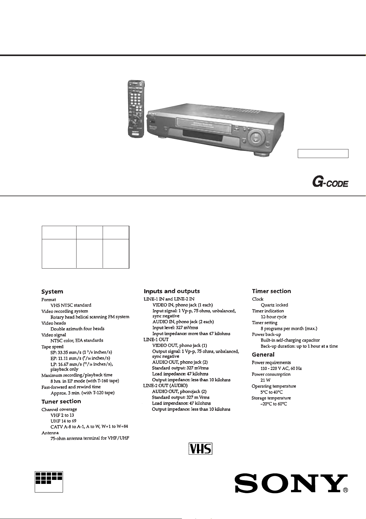
SLV-ED8KR/ED9KR
RMT-V244/V246
SERVICE MANUAL
Photo: SLV-ED8KR
• Refer to the SERVICE MANUAL of VHS MECHANICAL
ADJUSTMENTS VI for MECHANICAL ADJUSTMENTS.
(9-921-647-11)
* The abbreviations of ED8 and ED9 contained in this service manual are indi-
cated when these models are common to all their corresponding models as
given below.
Abbreviated
model name
All model
names
SLV-
ED8
ED8KR
ED9
ED9KR
Korean Model
S MECHANISM
G
SPECIFICATIONS
– Continued on next page –
VIDEO CASSETTE RECORDER
MICROFILM
SAFETY CHECK-OUT
After correcting the original service problem, perform the following
safety checks before releasing the set to the customer:
1. Check the area of your repair for unsoldered or poorly-soldered connections. Check the entire board surface for solder
splashes and bridges.
2. Check the interboard wiring to ensure that no wires are
“pinched” or contact high-wattage resistors.
3. Look for unauthorized replacement parts, particularly transistors, that were installed during a previous repair. Point them
out to the customer and recommend their replacement.
SAFETY-RELATED COMPONENT WARNING!!
COMPONENTS IDENTIFIED BY MARK ! OR DOTTED
LINE WITH MARK ! ON THE SCHEMATIC DIAGRAMS
AND IN THE PARTS LIST ARE CRITICAL TO SAFE
OPERATION. REPLACE THESE COMPONENTS WITH
SONY PARTS WHOSE PART NUMBERS APPEAR AS
SHOWN IN THIS MANUAL OR IN SUPPLEMENTS PUBLISHED BY SONY.
4. Look for parts which, though functioning, show obvious signs
of deterioration. Point them out to the customer and recommend their replacement.
5. Check the B+ voltage to see it is at the values specified.
– 2 –

TABLE OF CONTENTS
Section Title Page Section Title Page
SERVICE NOTE...................................................................... 4
5. INTERFACE, IC PIN FUNCTION DESCRIPTION
1. GENERAL
Getting Started .............................................................. 1-1
Basic Operations ........................................................... 1-5
Additional Operations.................................................... 1-8
Editing............................................................................ 1-11
Additional Information ................................................... 1-12
2. DISASSEMBLY
2-1. Upper Case Removal.................................................... 2-1
2-2. RJ-79, NK-11 Board Removal....................................... 2-1
2-3. Rear Panel Removal ..................................................... 2-1
2-4. Front Panel Section Removal ....................................... 2-1
2-5. FR-137, DM-77, SW-307, IO-64 Board
Removal (ED9).............................................................. 2-2
2-6. Control Switch Block Removal (ED9) ........................... 2-2
2-7. FR-137, DM-77, IO-64 Board Removal (ED8) ............. 2-2
2-8. Mechanism Deck Removal ........................................... 2-2
2-9. Power Block Removal ................................................... 2-3
2-10. PS-414, MA-325 board Removal .................................. 2-3
2-11. Internal Views................................................................ 2-4
2-12. Circuit Boards Location ................................................. 2-5
3. BLOCK DIAGRAMS
3-1. Overall Block Diagram .................................................. 3-1
3-2. Video1 Block Diagram ................................................... 3-4
3-3. Video2 Block Diagram ................................................... 3-5
3-4. Servo/System control Block Diagram ........................... 3-7
3-5. Audio Block Diagram..................................................... 3-9
3-6. Tuner Block Diagram ..................................................... 3-11
3-7. Mode Control Block Diagram ........................................ 3-13
3-8. Power Block Diagram.................................................... 3-15
4. PRINTED WIRING BOARDS AND
SCHEMATIC DIAGRAMS
4-1. Frame Schematic Diagram ........................................... 4-3
4-2. Printed Wiring Boards and Schematic Diagrams ......... 4-5
MA-325 (Head Amp) Schematic Diagram .................... 4-5
MA-325 Printed Wiring Board ....................................... 4-9
MA-325 (Video, Audio) Schematic Diagram................. 4-11
MA-325 (System Control) Schematic Diagram ............ 4-15
MA-325 (Servo Control) Schematic Diagram ............... 4-17
MA-325 (Bias, CTL) Schematic Diagram ..................... 4-19
MA-325 (Hi-Fi Audio) Schematic Diagram .................... 4-21
MA-325 (OSD) Schematic Diagram.............................. 4-23
MA-325 (IO) , RJ-79 Schematic Diagrams and
RJ-79 Printed Wiring Board .......................................... 4-25
MA-325 (Tuner) Schematic Diagram ............................ 4-27
NK-11 Printed Wiring Board and
Schematic Diagram ....................................................... 4-29
DM-77, IO-64 Printed Wiring Boards and
Schematic Diagrams ..................................................... 4-31
FR-137, SW-307 Printed Wiring Boards....................... 4-33
FR-137, SW-307 Schematic Diagram .......................... 4-35
PS-414 Printed Wiring Board........................................ 4-37
PS-414 Schematic Diagram.......................................... 4-39
SR-718 Printed Wiring Board ....................................... 4-41
SR-718 Schematic Diagram ......................................... 4-43
5-1. System Control-Video Block Interface
(MA-325 board IC161) .................................................. 5-1
5-2. System Control-Servo Peripheral Circuit Interface
(MA-325 board IC161) .................................................. 5-1
5-3. System Control-Mechanism Block Interface
(MA-325 board IC161) .................................................. 5-2
5-4. System Control-System Control Peripheral Circuit
Interface (MA-325 board IC161) ................................... 5-3
5-5. System Control-Hi-Fi Audio Block Interface
(MA-325 board IC161) .................................................. 5-3
5-6. Servo/System Control Microprocessor Pin Function
(MA-325 board IC161) .................................................. 5-4
5-7. Timer/Tuner Control Microprocessor Pin Function
(FR-137 board IC301) ................................................... 5-5
5-8. KOREAN Processor Pin Function
(NK-11 board IC1) ......................................................... 5-6
6. ERROR CODE.......................................................... 6-1
7. ADJUSTMENTS
7-1. Mechanical Adjustments ............................................... 7-1
7-2. Adjustments................................................................... 7-1
2-1. EEP ROM Initial Data Input .......................................... 7-1
7-3. Electrical Adjustments................................................... 7-1
3-1. Pre-Adjustment Preparations........................................ 7-1
3-1-1. Instruments to be Used............................................ 7-1
3-1-2. Connection ............................................................... 7-1
3-1-3. Set-up of Adjustment ............................................... 7-2
3-1-4. Alignment T apes....................................................... 7-2
3-1-5. Specified I/O Level and Impedance
Input/Output T erminal............................................... 7-2
3-1-6. Adjusting Sequence ................................................. 7-2
3-2. Power Supply Adjustment ............................................. 7-2
3-2-1. Power Supply Check................................................ 7-2
3-2-2. +6 V Adjustment ....................................................... 7-2
3-3. Servo System Adjustment............................................. 7-3
3-3-1. RF Switching Position Adjustment........................... 7-3
3-4. Audio System Adjustments ........................................... 7-3
3-4-1. Hi-Fi Audio System Adjustment ............................... 7-3
1. AF Switching Position Adjustment........................... 7-3
2. Frequency Response Check.................................... 7-4
3. Overall Level Characteristic and
Distortion Factor Check ........................................... 7-4
4. Overall S/N Check.................................................... 7-4
3-4-2. Normal Audio System Adjustment ........................... 7-5
1. ACE Head Adjustment ............................................. 7-5
2. E-E Output Level Check........................................... 7-5
3. Frequency Responce Check.................................... 7-5
4. Overall Level Characteristic and Distortion
Factor Check ............................................................ 7-5
5. Overall S/N Check.................................................... 7-5
3-5. Video System Adjustment ............................................. 7-5
3-5-1. VCO Oscillation Frequency Adjustment .................. 7-5
3-6. Parts Arrangement Diagram for Adjustments............... 7-6
8. REPAIR PARTS LIST
8-1. Exploded Views ............................................................. 8-1
8-1-1. Front Panel and Cabinet Assemblies (ED8)............ 8-1
8-1-2. Front Panel and Cabinet Assemblies (ED9)............ 8-2
8-1-3. Chassis Assembly .................................................... 8-3
8-1-4. Mechanism Chassis Assembly (1)........................... 8-4
8-1-5. Mechanism Chassis Assembly (2)........................... 8-5
8-1-6. Mechanism Chassis Assembly (3)........................... 8-6
8-2. Electrical Parts List........................................................ 8-7
– 3 –
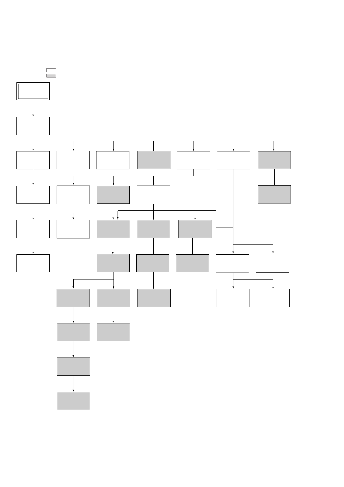
SERVICE NOTE
1. DISASSEMBLY
• This set can be disassembled in the order shown below.
Note: Pages in indicated pages in the SERVICE MANUAL.
Pages in indicated pages in the VHS MECHANICAL ADJUSTMENT MANUAL VI.
Set
Upper case
(Page 2-1)
Front Panel
Section
(Page 2-1)
FR-137 Board
(Page 2-2)
IO-64 Board
(Page 2-2)
Control Switch
Block (ED9)
(Page 2-2)
RJ-79 Board
(Page 2-1)
DM-77 Board
(Page 2-2)
SW-307 Board
(ED9)
(Page 2-2)
Cam Gear
(Page 23)
NK-11 Board
(Page 2-1)
FL complete
Ass’y
(Page 13)
Retainer
Plate
(Page 22)
FL Slider
Block Ass’y
(Page 22)
Cam Motor
Retainer
(Page 31)
Pinch Press
Block Ass’y
(Page 14)
Mechanism
Deck
(Page 2-2)
Rubber
Belt
(Page 15)
Pully Gear
Ass’y
(Page 29)
Reel Direct
Ass’y
(Page 30)
Rear Panel
(Page 2-1)
Rubber
Belt
(Page 15)
Capstan
Motor
(Page 15)
Power
Block
(Page 2-3)
MA-325 Board
(Page 2-3)
Rotary
Switch
(Page 2-2)
Ground Shaft
Ass’y
(Page 13)
Drum Ass’y
(Page 13)
PS-414 Board
(Page 2-3)
Tuner
Unit
Rubber
Belt
(Page 15)
Slider
(Page 26)
Loading
Gear (T, S)
(Page 28)
Cam Motor
(Page 31)
– 4 –
SECTION 1
GENERAL
SLV-ED8/ED9
This section is extracted from SLV -ED8KR
instruction manual (3-861-812-11).
1-1
1-2
1-3
1-4
1-5
1-6
1-7
1-8
1-9
1-10
1-11
1-12
1-13
1-13 E
SECTION 2
DISASSEMBLY
Note: Follow the disassembly procedure in the numerical order given.
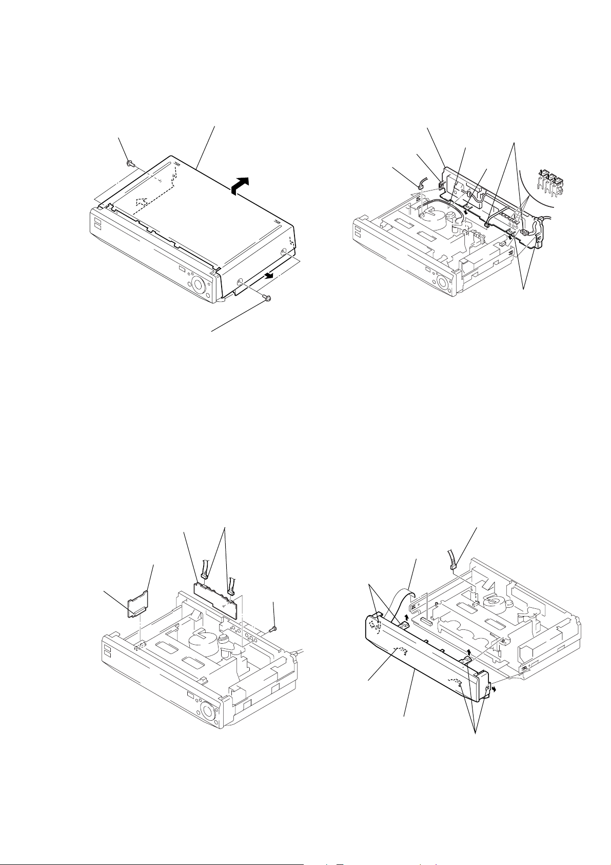
2-1. UPPER CASE REMOVAL 2-3. REAR PANEL REMOVAL
SLV-ED8/ED9
1 Two tapping screws
2 Two tapping screws
3 Upper case
2 Connector
(CN361)
8 Rear panel
7 Claw
3 Harness
6 Claw
1 Two connectors
(CN101, 901)
4 Three claws
5 Two claws
2-2. RJ-79, NK-11 BOARD REMOVAL
1 Two connectors
3 RJ-79 board
5 NK-11 board
4 Connector
(CN751)
(CN951, 952)
2 Four screws
(BVTP3 × 12)
2-4. FRONT PANEL SECTION REMOVAL
1 Connector
(CN423)
2 Flat cable
(CN105)
3 Two claws
4 Claw
6 Front panel section
5 Three claws
2-1
2-5. FR-137, DM-77, SW-307, IO-64 BOARD
REMOVAL (ED9)
2-7. FR-137, DM-77, IO-64 BOARD
REMOVAL (ED8)
!¡ SW-307 board
5 Flat cable
(CN308)
4 FR-137 board
0 Two screws
(B2.6 × 8)
3 Four screws
(B2.6 × 8)
1 Flat cable
!™ IO-64
board
6 Flexible board
(CN302)
9 Flexible board
(CN451)
2 Screw
(B2.6 × 8)
(CN309)
8 DM-77 board
7 Four screws
(B2.6 × 8)
7 Screw
(B2.6 × 8)
8 IO-64 board
3 FR-137 board
1 Nine screws
(B2.6 × 8)
6 DM-77 board
5 Connector
(CN307)
2 Four screws
(B2.6 × 8)
4 Flexible board
(CN451)
2-6. CONTROL SWITCH BLOCK REMOVAL
(ED9)
1 Two screws
2 Damper holder
5 Control switch block
(B2.6 × 8)
4 Fulcrum plate
(right) assembly
3 Screw
(B2.6 × 8)
2-8. MECHANISM DECK REMOVAL
2 Connector
3 Connector
(FE head)
6 Two screws
(BVTP3 × 12)
7 Mechanism deck
4 Screw
(B3)
Note: When mounting the mechanism deck,
first align ¢ mark on the rotary switch.
(ACE head)
5 Screw
(BVTP3 × 12)
1 Flexible board
2-2
2-9. POWER BLOCK REMOVAL
2 Two screws
(B3)
3 Power block
1 Power cord
2-10. PS-414, MA-325 BOARD REMOVAL
5 Three screws
(B3)
6 MA-325 board
4 Screw
1 Connector
(CN162)
2 Three screws
(B3)
(B3)
3 PS-414 board
2-3
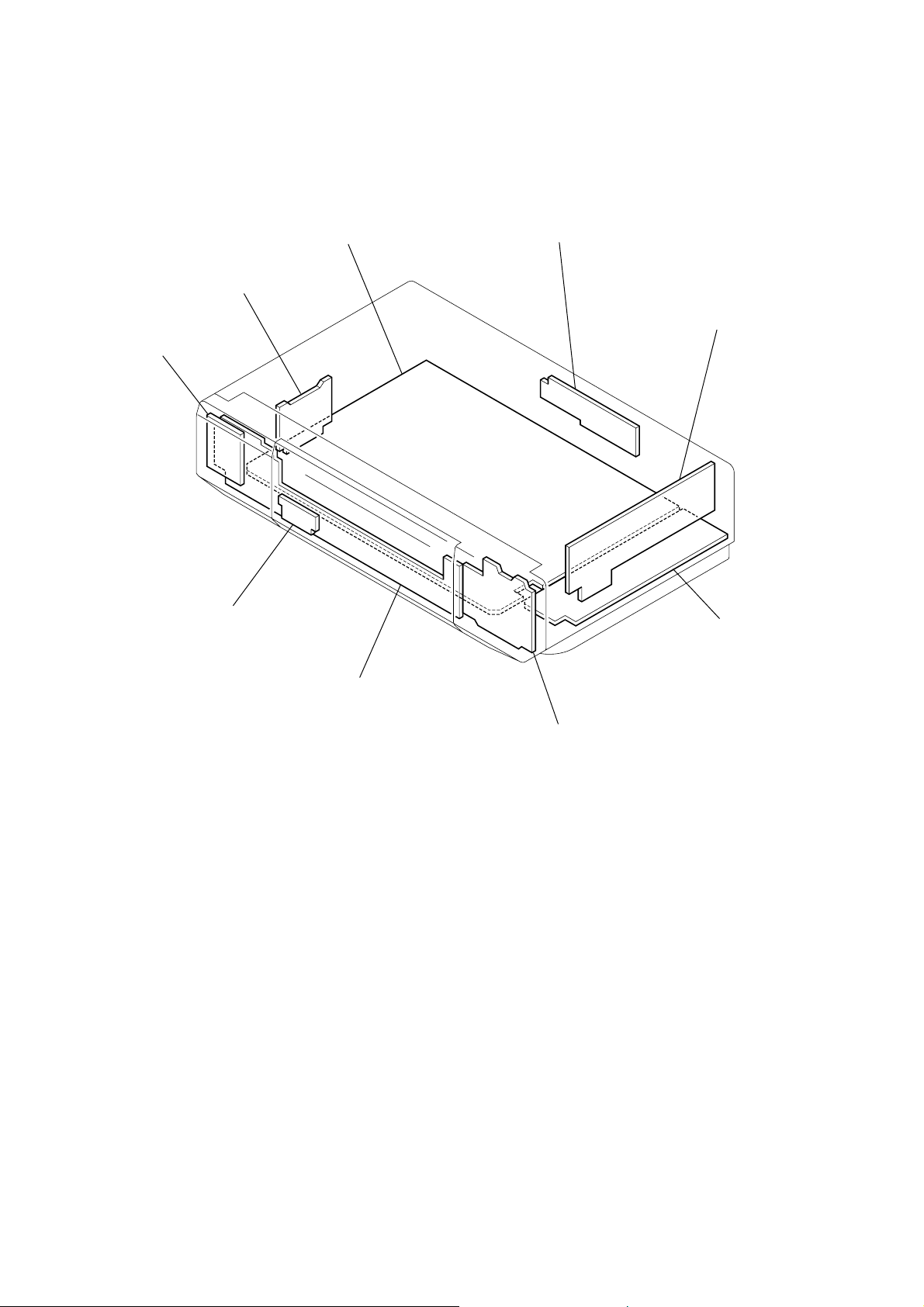
2-11. INTERNAL VIEWS
Drum assembly (M901) (DZH-94A/ZRP)
8-839-044-02
FE head
1-500-144-11
Q100
Tape end sensor
8-729-043-84
M902
Capstan motor
1-698-971-11
Q101
Tape top sensor
8-729-043-84
D102
Tape top/end LED
8-719-048-26
Drum assembly (M901) (DZH-94A/ZRP)
8-839-044-02
M903
Cam motor assembly
X-3947-577-1
2-4
2-12. CIRCUIT BOARDS LOCATION
MA-325
VIDEO, AUDIO, I/O,
(
SERVO/SYSTEM CONTROL, TUNER
RJ-79
)
(ADDITIONAL REAR OUT)
NK-11
(KOREAN STEREO)
SW-307 (ED9)
(POWER SWITCH)
IO-64
(FRONT IN)
FR-137
FL DRIVE,
(
MODE CONTROL
)
DM-77
(MODE CONTROL)
POWER BLOCK
(SR-718)
(SWITCHING REGULATOR)
PS414
(POWER SUPPLY)
2-52-5 E
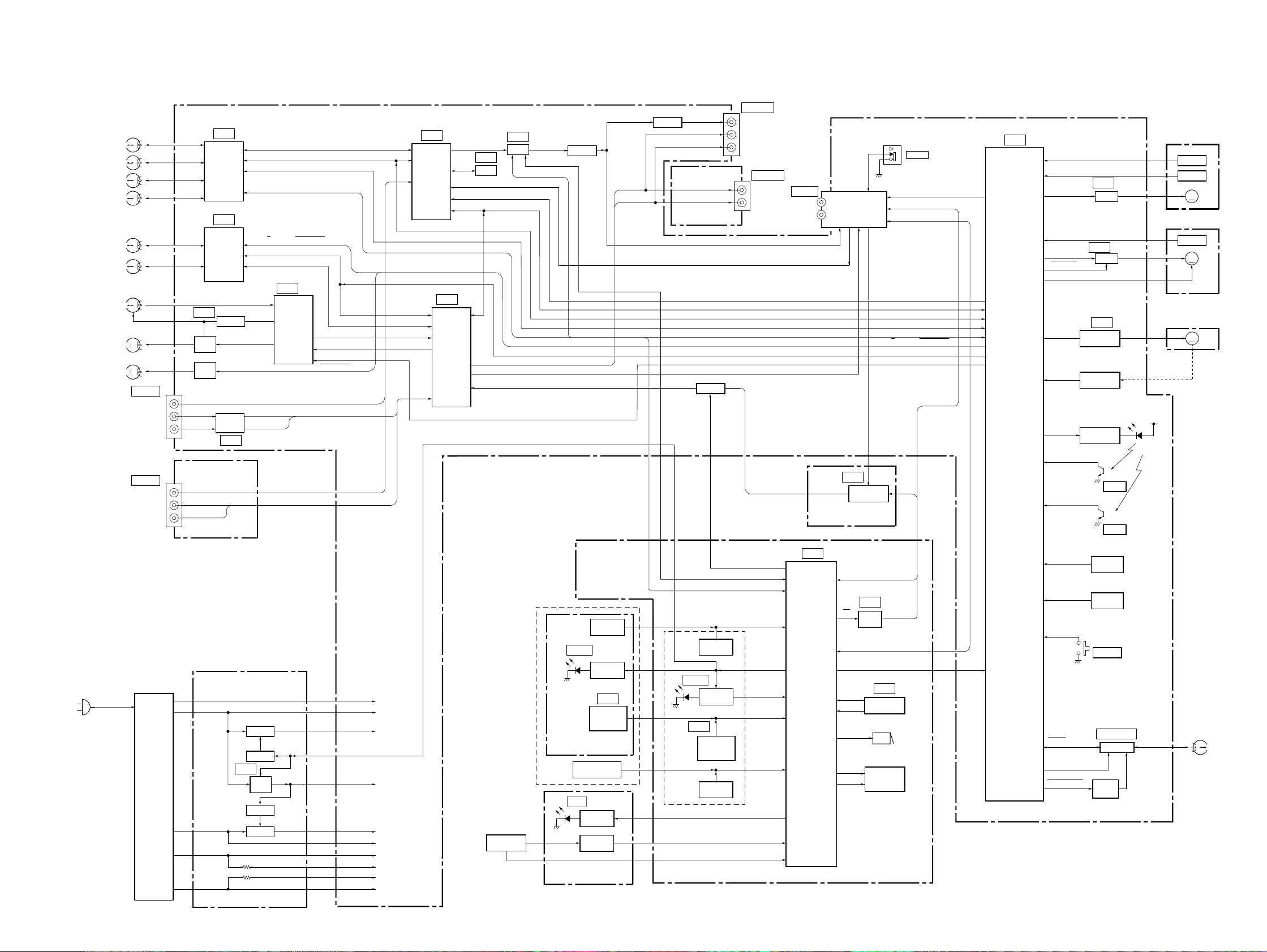
3-1. OVERALL BLOCK DIAGRAM
SLV-ED8/ED9
SECTION 3
BLOCK DIAGRAMS
SP CH1
SP CH2
EP CH1
EP CH2
CH1
CH2
MONO
AUDIO HEAD
AUDIO
ERASE HEAD
FULL
ERASE HEAD
VIDEO
HEAD
Hi-Fi
AUDIO HEAD
LINE 1 IN
VIDEO
AUDIO L
AUDIO R
LINE 2 IN
VIDEO
AUDIO L
AUDIO R
MA-325 BOARD
(SEE PAGE 4-5~4-28)
REC/PB
REC/PB
IC071
T081
BIAS
OSC
T091
BIAS
OSC
CNJ901
L1 IN V
L1 IN L
L1 IN R
IO-64 BOARD
(SEE PAGE 4-32)
CNJ480
L2 IN V
L2 IN L
L2 IN R
IC501
VIDEO
AMP
IC340
AUDIO
AMP
SWITCH
BUFFER
IC901
REC RF, PB RF, CROT
COMP SYNC
RF ENV, RF SWP
SCK, SO
AF RECP, AF RFC, FULL ERASE
AF SWP
AFM REC, PB AFM
IC201
NA HEAD PB
NA REC
BIAS VCC
L1 IN L
L1 IN R
AUDIO
PROCESSOR
(MONO)
(1/2)
NORMAL AU
NA HF OUT
A MUTE
FULL ERASE
IC201
Y/C
PROCESSOR
PROCESSOR
(2/2)
VIDEO OUT
TV VIDEO
QVD
IIC CLK, IIC DATA
IC360
AUDIO
(Hi-Fi)
IC401
OSD
IC202
CCD
LINE OUT L, LINE OUT R
MOD A
TUNER L
TUNER R
OSD V
CGV, HDET,
CG CS
SCK, SI
Q401
BUFFER
LINE OUT L
LINE OUT R
Q901
BUFFER
RJ-79 BOARD
(SEE PAGE 4-25)
Q751-Q753
CNJ901
CNJ953
MUTE
TA MUTE
LINE-1 OUT
VIDEO
AUDIO L
AUDIO R
LINE-2 OUT
AUDIO L
AUDIO R
TU701
VHF/UHF
IN
OUT
MOD V
TUNER/MODURATOR
VIDEO
L OUT, R OUT
NK-11 BOARD
(SEE PAGE 4-29)
S701
SIF
MOD A
AF RECP, AF RFC, FULL ERASE
IC 1
KOREAN
STEREO
RF UNIT
SDA0,SCL0
PLL DATA,
PLL CLK,
PL ENABLE,
AFT, SAP,
FMONO
IIC CLK, IIC DATA
COMP SYNC
RF ENV, RF SWP
QVD
SCK, SO
AF SWP
A MUTE
TV/VTR
IC161
SERVO/SYSTEM
CONTROL
D FG
D PG
DRM DA
CAP FG
CAP DA
CAP STOP
CAP RVS, CAP TRQ PWM
CAM
MODE1-4
T/S LED
T SENS
S SENS
IC101
AMP
IC101
AMP
IC130
CAM MOTOR
DRIVER
S100
ROTARY
SWITCH
Q111
LED
DRIVER
(2/2)
Q101
T SENS
Q101
S SENS
(1/2)
D VS
CAP VS
D102
M901
DRUM MOTOR
DRUM FG
DRUM PG
M
M902
CAPSTAN MOTOR
CAP FG
M
M903
CAM MOTOR
M
AC
110~240V
POWER
BLOCK
SR-718
35V
13V
6V
–13V
GND
PS-414 BOARD
(SEE PAGE 4-39)
Q600
SWITCH
Q601
SWITCH
IC600
12V
REC
Q603
SWITCH
Q602
SWITCH
UN30V
UN13V
MTR12V
POWER CONT
SW12V
SW5V
D6V
–13V
GND
FR-137 BOARD
(SEE PAGE 4-35)
ED9
FUNCTION
SWITCH
POWER
Q400
LED
DRIVER
IC400
REMOTE
CONTROL
RECEIVER
SW-307 BOARD
(SEE PAGE 4-35)
OPERATING
SWITCH BLOCK
JOG
LED
DRIVER
CLIK
SHUTTLE
–F
+F
FUNCTION
SWITCH
DM-77 BOARD
(SEE PAGE 4-32)
ED8
POWER
IC304
FUNCTION
SWITCH
Q300
LED
DRIVER
REMOTE
CONTROL
RECEIVER
FUNCTION
SWITCH
TA MUTE
HDET, CGV, CG CS
SCK, SI, SO
A/D2
POWER CONT
SIRCS IN
A/D6, 7
LED CS
A/D0, 1
DMS1, 2
IC301
TIMER/TUNER/
MODE
CONTROL
SDA0, SCL0
IC303
WC
EEP
ROM
PLL DATA, PLL CLK,
PLL ENABLE,AFT
ASURA CS, ASURA RESET
POWER
FAIL
RESET
BUZZER
G1-G3
SEG1-6
IC302
RESET PULS
GENERATOR
BZ201
ND320
FLUORESCENT
INDICATOR
TUBE
T REEL FG
S REEL FG
REC PRE
PB CTL, REC CTL
CTL RESET
CTL HYS HIGH
PH100
T REEL
SENS
PH101
S REEL
SENS
S101
REC PRE
IC001, IC021
CTL AMP
Q001
GAIN
SWITCH
CTL HEAD
05
3-1 3-2
SLV-ED8/ED9
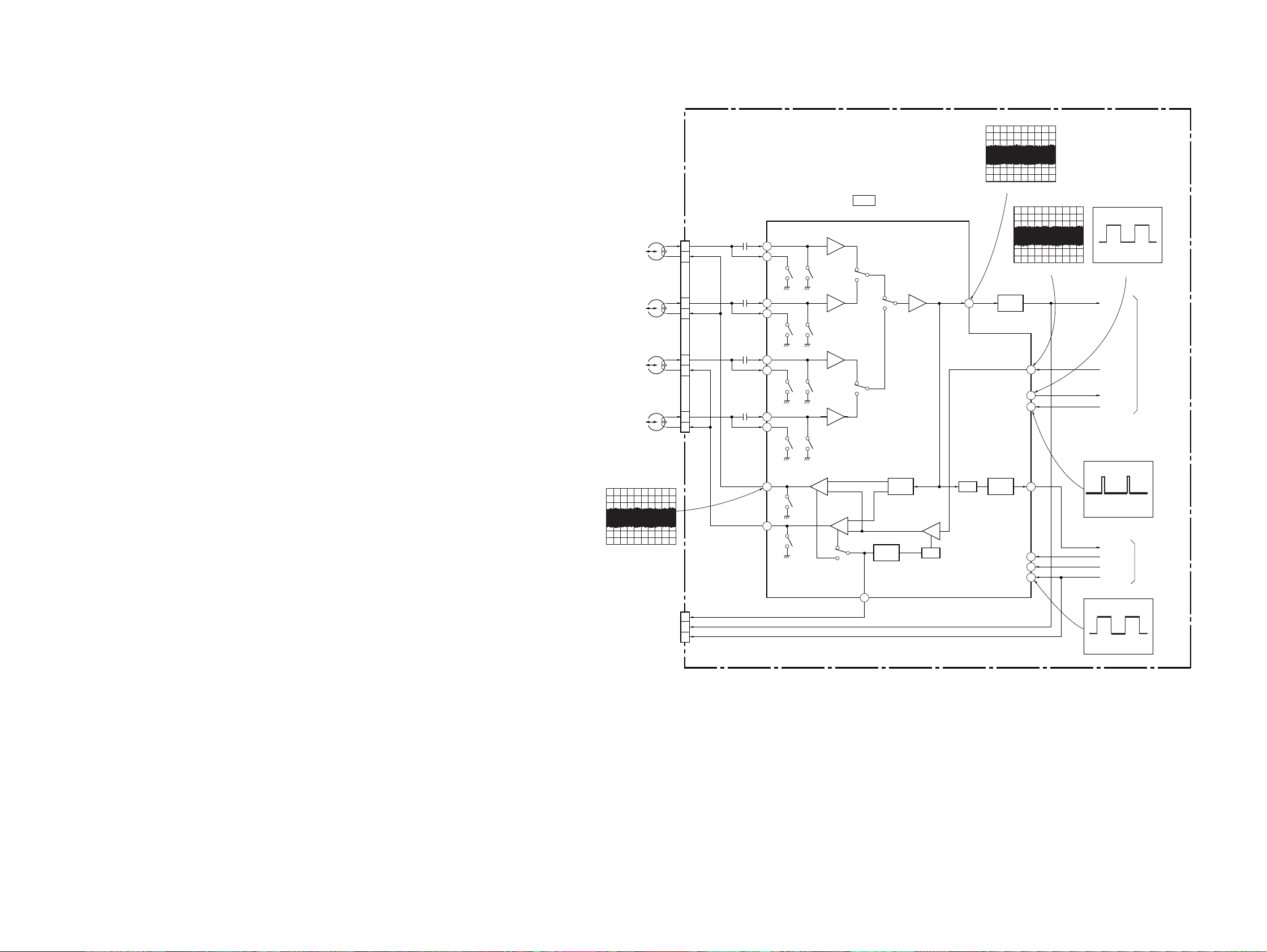
3-2. VIDEO1 BLOCK DIAGRAM
VIDEO
HEAD
SP
CH1
SP
CH2
EP
CH2
EP
CH1
IC5014 REC
3.4Vp-p (H)
CHECK
MA-325 BOARD (1/5)
(SEE PAGE 4-5)
CN502
SP CH1 F
3
SP CH1 S
4
SP CH2 F
7
SP CH2 S
8
EP CH2 F
1
EP CH2 S
2
EP
CH1 F
5
6
EP
CH1 S
CN501
REC CURR
1
REC RF
2
REC SWP
3
11
10
13
14
12
3
2
5
6
4
SW7
SW8
SW10
SW9
SW1
SW2
SW3
SW4
SW6
SW5
REC
IC501
VIDEO REC/PB AMP
PB
PB
PB
PB
REC
30
REC
ADJ
REC
IDEL
VCA
DET
HPF
IC501@™ PB
640mVp-p (H)
IC501 @• REC
88mVp-p (H)
Q501
22
PB RF
BUFF
C ROT
COMP SYNC
ENV
DET
SCK1 (SSB)
SO1 (SSB)
RF SWP
28
21
18
26
20
19
17
IC501 @¡ REC/PB
4.6Vp-p (2V)
PB RF
REC RF
C ROT
COMP SYNC
IC501 !• REC/PB
2.5Vp-p (H)
PB ENV
SCK1 (SSB)
SO1 (SSB)
RF SWP
IC501 !¶ REC/PB
VIDEO 2
(SEE PAGE 3-5)
SYSTEM
CONTROL
(SEE PAGE 3-8)
05
5.1Vp-p (2V)
3-4
3-3. VIDEO2 BLOCK DIAGRAM
SLV-ED8/ED9
MA-325 BOARD (2/5)
(SEE PAGE 4-11,4-23,4-25)
VIDEO 1
(SEE PAGE 3-4)
PB RF
REC RF
C ROT
COMP SYNC
IC201 !∞ PB
576mVp-p(H)
15
Q202
BUFFER
IC201 (1/2)
Y/C PROCESS
R
P
IC201 !¢ REC
C LPF
SEQ
PB EQ
R
P
KIL
S
N
1416
IC201 !• REC/PB
ACC
DET
ACC
AMP
SUB
CONV
17
Q203
BUFFER
MAIN
CONV
SUB
BPF
IC201 $™ REC/PB
REC:440mVp-p(H)
PB:400mVp-p(H)
1/2
BPF2
S
N
20
18
66
C ROT
P
R
FM
AGC
REC
EQ
IC201 @• REC
R
P
DOUB
MOD
LIM
YNRLPF
DL EQBPF1
R
DEM
FM
DE
EMH
SUB
LPF
NL
DE-EM
DHP
NC
P
25
CLP
26
5 7 4042
348
150
Q206
EMPH
DE
IC201 $• REC/PB
REC:320mVp-p(H)
PB:270mVp-p(H)
IC202
CCD DELAY
1H
DL
1H/2H
DL
13 52
10
CLK
IC202 7 REC/PB
400mVp-p(H)
Q208
BUFFER
Q204
BUFFER
Q201
BUFFER
3.58MHz
IC201 %∞ REC/PB
552mVp-p (3.58MHz)
CLP
X202
56
55
IC202!£ REC/PB
REC:360mVp-p (H)
PB:270mVp-p(H)
LPF
COMB
CTH
KIL
B.D.
NAP
BPF
REC
BGA
PB
BGA-B
R
P
VCLK (IIC)
VSDATA (IIC)
63
64
VCLK (IIC)
VSDATA (IIC)
CNJ901
LINE-1
IN
CNJ480
LINE-2
IN
VIDEO
VIDEO
IO-64 BOARD (1/2)
(SEE PAGE 4-32)
340mVp-p(H)
CN480
5 5
L2 VIDEO
PIC
1Vp-p(H)
310mVp-p(H)
CN423
05
28
30
32
TU VIDEO
34 35
+
TUNER
(SEE PAGE 3-11)
VIDEO
AGC
CTL
P
R
P
R
MIX
FBC
C
45
NC
Y/C
SYNC
SEP
QV/QH
INS
VIDEO
AMP
IC201 #¶ REC/PB
4.4Vp-p (H)
37
33
38
IC401 @º REC/PB
1.9 Vp-p (H)
IC401 @•REC/PB
IC401 !§,!• REC/PB
Q403, 404
BUFFER
2.0Vp-p ( H)
CLP
Q402
SYNC
SEP
SW5V
46
SYSTEM
CONTROL
TUNER
(SEE PAGE 3-11)
15
10
26
(SEE PAGE 3-8)
CNJ901
LINE-1
VIDEO
H DET
CG V
OSD CS
IC401 7 REC/PB
5.2 Vp-p (2V)
OUT
MODE
CONTROL
(SEE PAGE 3-14)
18
19
20
15
CV IN
CV CR
SYNC IN
RESET
VCO
OUT
IC401
OSD
V SYNC OUT
XTAL OUT1
28 27
S IN
S CLK
CV OUT
SYNC DET
XTAL IN1
VCO
IN
COMP SYNC
QVD
SI
S CLK
MOD V
9
10
Q401
BUFFER
16
29
7
8
CS
3
14.31818MHz
2
Q901
BUFFER
CN105
X401
IC401 2 REC/PB
CT401
VCO ADJ
3.6 Vp-p (13.89 MHz)
3-5 3-6
1.6Vp-p (14.32 MHz)
 Loading...