

Sony SGM2014AN Datasheet

Description
The SGM2014AN is an N-channel dual gate GaAs
MES FET for UHF band low-noise amplification.
This FET is suitable for a wide range of applications
including TV tuners, cellular radios, and DBS IF
amplifiers.
Features
• Ultra small package
• Low voltage operation
• Low noise: NF = 1.5dB (typ.) at 900MHz
• High gain: Ga = 18dB (typ.) at 900MHz
• Low cross-modulation
• High stability
• Built-in gate-protection diode
Application
UHF band amplifier, mixer and oscillator
Structure
GaAs N-channel dual-gate metal semiconductor field-effect transistor
Absolute Maximum Ratings (Ta = 25°C)
• Drain to source voltage VDSX 12 V
• Gate 1 to source voltage VG1S –5 V
• Gate 2 to source voltage VG2S –5 V
• Drain current ID 55 mA
• Allowable power dissipation PD 100 mW
• Channel temperature Tch 125 °C
• Storage temperature Tstg –55 to +150 °C
– 1 –
SGM2014AN
E97938-PS
GaAs N-channel Dual Gate MES FET
Sony reserves the right to change products and specifications without prior notice. This information does not convey any license by
any implication or otherwise under any patents or other right. Application circuits shown, if any, are typical examples illustrating the
operation of the devices. Sony cannot assume responsibility for any problems arising out of the use of these circuits.
M-281
For the availability of this product, please contact the sales office.
– 2 –
SGM2014AN
Typical Characteristics (Ta = 25°C)
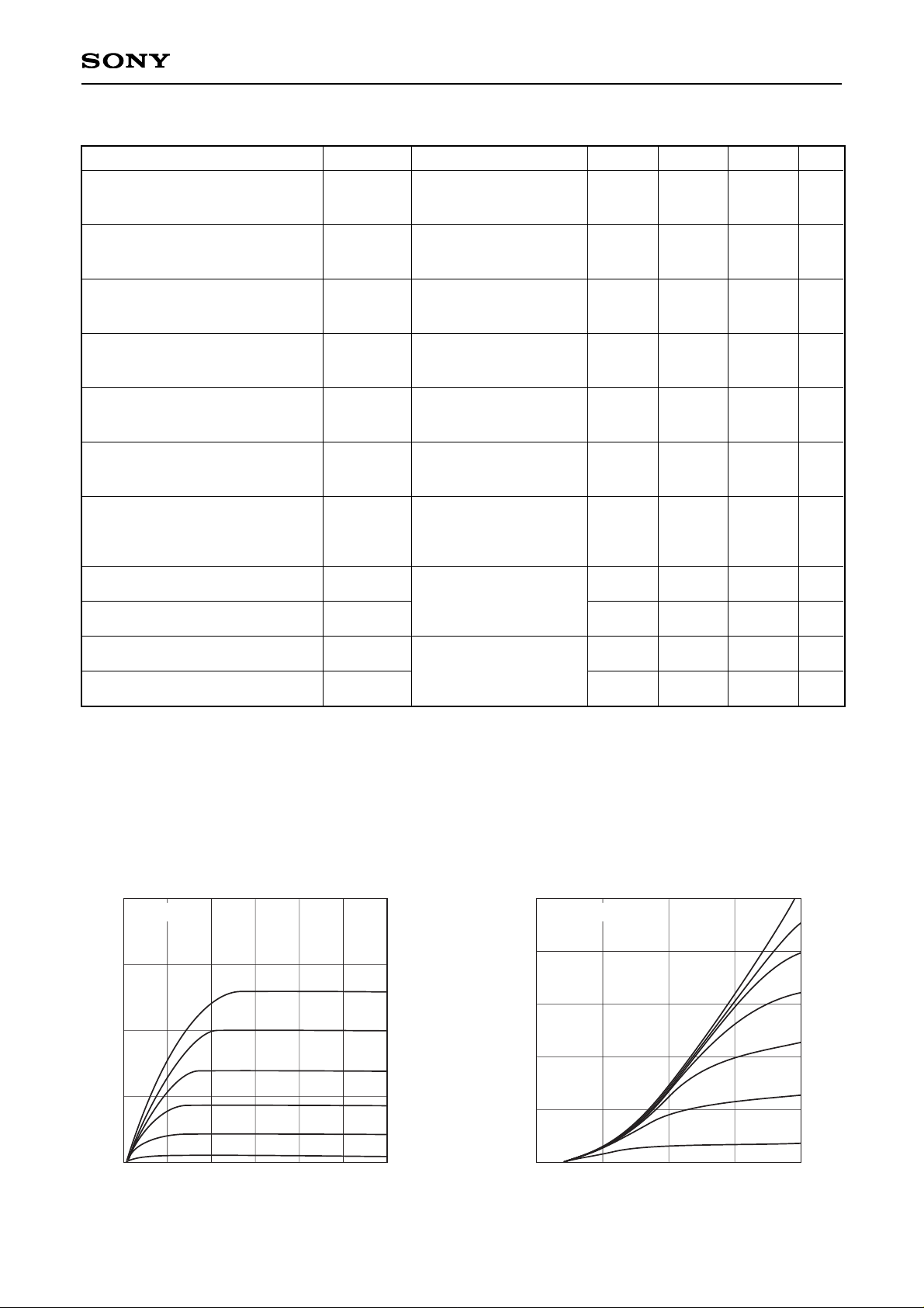
Electrical Characteristics (Ta = 25°C)
Item
Drain cut-off current
Gate 1 to source current
Gate 2 to source current
Drain saturation current
Gate 1 to source cut-off voltage
Gate 2 to source cut-off voltage
Forward transfer admittance
Input capacitance
Feedback capacitance
Noise figure
Associated gain
IDSX
IG1SS
IG2SS
IDSS
VG1S (OFF)
VG2S (OFF)
gm
Ciss
Crss
NF
Ga
VDS = 12V
VG1S = –4V
VG2S = 0V
VG1S = –4.5V
VG2S = 0V
VDS = 0V
VG2S = –4.5V
VG1S = 0V
VDS = 0V
VDS = 5V
VG1S = 0V
VG2S = 0V
VDS = 5V
ID = 100µA
VG2S = 0V
VDS = 5V
ID = 100µA
VG1S = 0V
VDS = 5V
ID = 10mA
VG2S =1.5V
f = 1kHz
VDS = 5V
ID = 10mA
VG2S = 1.5V
f = 1MHz
VDS = 5V
ID = 10mA
VG2S = 1.5V
f = 900MHz
8
13
15
17
0.9
25
1.5
18
50
–8
–8
28
–2.5
–2.5
2
50
2.5
µA
µA
µA
mA
V
V
ms
pF
fF
dB
dB
Symbol Condition Min. Typ. Max. unit
40
(VG2S = 1.5V)
30
20
– Drain current [mA]
D
I
10
0
0 1 2 3 4 5 6
V
DS – Drain to source voltage [V]
ID vs. VDS
VG1S
= 0V
–0.3V
–0.6V
–0.9V
–1.2V
–1.5V
ID vs. VG1S
25
(VDS = 5V)
20
15
10
– Drain current [mA]
D
I
5
0
–2.0 –1.5 –1.0 –0.5 0
V
G1S – Gate 1 to source voltage [V]
V
G2S
= 1.5V
1.0V
0.5V
0V
–0.5V
–1.0V
–1.5V
 Loading...