

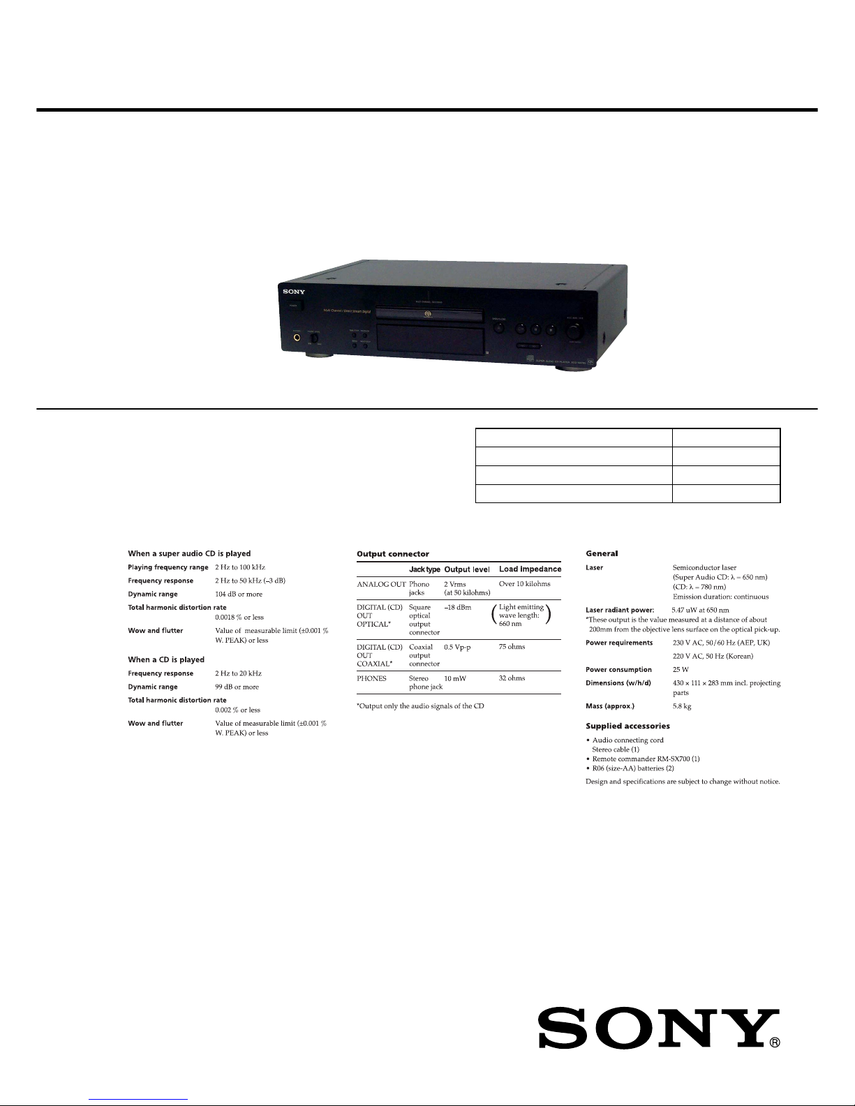
Sony SCD-XB780,SCD-XB790 Service Manual
SERVICE MANUAL
SUPER AUDIO CD PLAYER
AEP Model
UK Model
Korean Model
SCD-XB780
Ver 1.3 2002.11
SPECIFICATIONS
Model Name Using Similar Mechanism NEW
CD Mechanism Type CDM66B-DVBU6B
Base Unit Name DVBU-6B
Optical Pick-up Name KHM-234AMA
9-873-930-04 Sony Corporation
2002K0500-1 Home Audio Company
C 2002.11 Published by Sony Engineering Corporation
2
SCD-XB780
This appliance is classified as a CLASS 1
LASER product.
This label is located on the rear exterior.
The following caution label is located
inside the unit.
SAFETY-RELATED COMPONENT WARNING!!
COMPONENTS IDENTIFIED BY MARK 0 OR DOTTED
LINE WITH MARK 0 ON THE SCHEMATIC DIAGRAMS
AND IN THE PARTS LIST ARE CRITICAL TO SAFE
OPERATION. REPLACE THESE COMPONENTS WITH
SONY PARTS WHOSE PART NUMBERS APPEAR AS
SHOWN IN THIS MANUAL OR IN SUPPLEMENTS PUBLISHED BY SONY.
Notes on chip component replacement
•Never reuse a disconnected chip component.
• Notice that the minus side of a tantalum capacitor may be damaged by heat.
Flexible Circuit Board Repairing
•Keep the temperature of the soldering iron around 270 ˚C during repairing.
• Do not touch the soldering iron on the same conductor of the
circuit board (within 3 times).
• Be careful not to apply force on the conductor when soldering
or unsoldering.
TABLE OF CONTENTS
1. SERVICING NOTES ............................................... 3
2. GENERAL ................................................................... 6
3. DISASSEMBLY
3-1. Disassembly Flow ........................................................... 8
3-2. Case ................................................................................. 9
3-3. Front Panel Section ......................................................... 9
3-4. AUDIO Board, MAIN Board.......................................... 10
3-5. Mechanism Deck (CDM66B-DVBU6B) ....................... 10
3-6. Base Unit (DVBU-6B).................................................... 11
4. TEST MODE.............................................................. 12
5. DIAGRAMS
5-1. Block Diagram – RF/SERVO Section – ........................ 20
5-2. Block Diagram – SERVO Section – .............................. 21
5-3. Block Diagram – MAIN Section – ................................ 22
5-4. Block Diagram – AUDIO Section – .............................. 23
5-5. Block Diagram – DISPLAY/KEY CONTROL/
POWER SUPPLY Section – ........................................... 24
5-6. Notes for Printed Wiring Boards and
Schematic Diagrams ....................................................... 25
5-7. Schematic Diagram – RF Board – ................................. 26
5-8. Printed Wiring Boards
– RF/LOADING Boards – .............................................. 27
5-9. Printed Wiring Board
– MAIN Board (Component Side) – .............................. 28
5-10. Printed Wiring Board
– MAIN Board (Conductor Side) – ................................ 29
5-11. Schematic Diagram
– MAIN (1/5)/ LOADING Boards – ............................. 30
5-12. Schematic Diagram – MAIN Board (2/5) –.................. 31
5-13. Schematic Diagram – MAIN Board (3/5) –.................. 32
5-14. Schematic Diagram – MAIN Board (4/5) –.................. 33
5-15. Schematic Diagram – MAIN Board (5/5) –.................. 34
5-16. Schematic Diagram – AUDIO/HP Boards – ................. 35
5-17. Printed Wiring Board
– AUDIO Board (Component Side) – ............................ 36
5-18. Printed Wiring Boards
– AUDIO (Conductor Side)/HP Boards – ..................... 37
5-19. Printed Wiring Boards – DISPLAY/KEY Boards –...... 38
5-20. Schematic Diagram – DISPLAY/KEY Boards – .......... 39
5-21. Printed Wiring Boards
– POWER/POWER SW/PT Boards – ............................ 40
5-22. Schematic Diagram
– POWER/POWER SW/PT Boards – ............................ 41
5-23. IC Pin Function Description........................................... 49
6. EXPLODED VIEWS
6-1. Case Section .................................................................... 61
6-2. Front Panel Section ......................................................... 62
6-3. Chassis Section ............................................................... 63
6-4. Mechanism Deck Section (CDM66B-DVBU6B) .......... 64
6-5. Base Unit Section (DVBU-6B)....................................... 65
7. ELECTRICAL PARTS LIST ............................... 66
CAUTION
Use of controls or adjustments or performance of procedures
other than those specified herein may result in hazardous radiation exposure.
3
SCD-XB780
The laser diode in the optical pick-up block may suffer electrostatic break-down because of the potential difference generated
by the charged electrostatic load, etc. on clothing and the human
body.
During repair, pay attention to electrostatic break-down and also
use the procedure in the printed matter which is included in the
repair parts.
The flexible board is easily damaged and should be handled with
care.
NOTES ON LASER DIODE EMISSION CHECK
The laser beam on this model is concentrated so as to be focused
on the disc reflective surface by the objective lens in the optical
pick-up block. Therefore, when checking the laser diode emission, observe from more than 30 cm away from the objective lens.
CLEANING OF OPTICAL PICK-UP LENS
In cleaning the lens of optical pick-up, use the air blower.
Never use a cotton swab for cleaning the lens of optical pick-up,
which otherwise causes a trouble.
NOTES ON HANDLING THE OPTICAL PICK-UP
BLOCK OR BASE UNIT
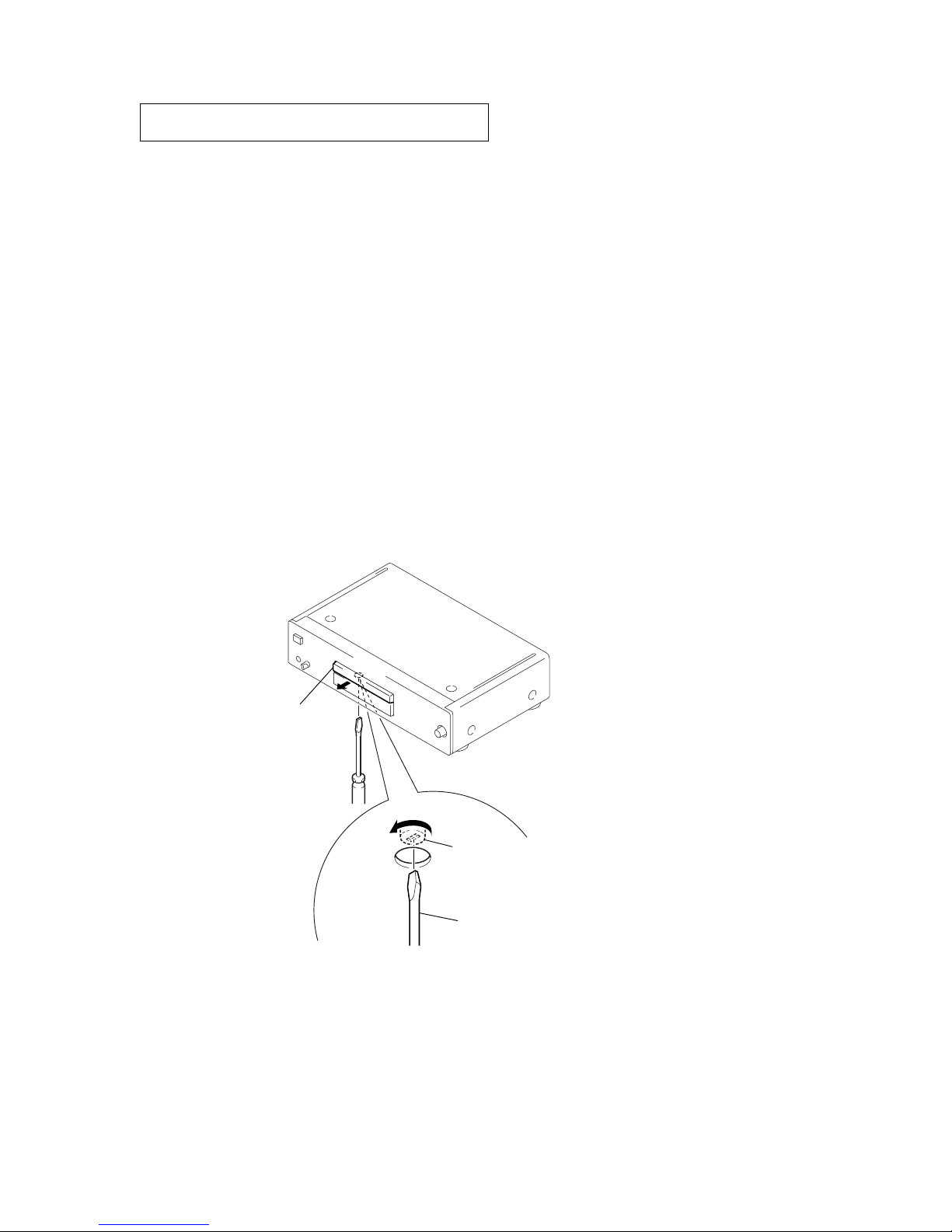
HOW TO OPEN THE TRAY WHEN POWER SWITCH TURNS OFF
tray
tapering driver
cam (66)
1
Insert a tapering driver (3 mm in diameter)
in the hole at the bottom of the unit,
turn the cam (66) fully in the direction of arrow A.
A
SECTION 1
SERVICING NOTES
4
SCD-XB780
DISPLAY BOARD SERVICE POSITION
In checking the DISPLAY board, prepare jig (extension cable J-2501-200-A : 1.00 mm Pitch, 11 cores, Length 300 mm.)
MAIN board
DISPLAY board
CN801
Connect jig (extension cable J-2501-200-A)
to the DISPLAY board (CN801) and
MAIN board (CN706).
CN706
Note: Follow the assembly procedure in the numerical order given.
INSTALLATION OF THE TRANS BOARD
3
four screws
(PTTWH3
×
6)
2
power transformer
(T902)
4
3
four screws
(PTTWH3
×
6)
1
power transformer
(T901)
5
Solder seventeen portions.
Note : Solder the TRANS board after installing power transformers (T901, T902)
to the chassis.
(To prevent the TRANS board from being cracked.)

5
SCD-XB780
RESETTING OPERATION AT POWER ON
If the power is turned on with a disc loaded in the set, a sequence of operation as shown below will be performed.
(The operation varies depending on the type of disc) Condition: continue mode
(1) CD
1. Sled reverse move (sled in)
2. Disc detect
3. IC setting for CD
4. Servo error signal offset auto adjustment
5. Spindle kick for LD on
6. LD on
7. Focus search
8. Focus servo on
9. Spindle kick
10. Spindle ser vo on
11. E-F balance auto adjustment
12. Tracking & sled servo on
13. Focus bias auto adjustment
14. Focus servo gain auto adjustment
15. Tracking servo gain auto adjustment
16. Jump to lead-in area
17. Read TOC
18. Stop
(2) SACD (single layer)
1. Sled reverse move (sled in)
2. Disc detect
3. IC setting for SACD
4. Servo error signal offset auto adjustment
5. Spindle kick for LD on
6. LD on
7. Focus search
8. Focus servo on
9. Spindle kick
10. Spindle ser vo on
11. E-F balance auto adjustment
12. Tracking & sled servo on
13. Focus bias auto adjustment
14. Focus servo gain auto adjustment
15. Tracking servo gain auto adjustment
16. Jump to lead-in area
17. Read TOC
18. Stop
(3) SACD (dual layer)
1. Sled reverse move (sled in)
2. Disc detect
3. IC setting for SACD
4. Servo error signal offset auto adjustment
5. Spindle kick for LD on
6. LD on
7. Focus search
8. Focus servo on (layer 0)
9. Spindle kick
10. Spindle servo on
11. E-F balance auto adjustment (layer 0)
12. Tracking & sled servo on (layer 0)
13. Focus bias auto adjustment (layer 0)
14. Focus servo gain auto adjustment (layer 0)
15. Tracking servo gain auto adjustment (layer 0)
16. Jump to lead-in area
17. Read TOC
18. Focus jump (layer 0tlayer 1)
19. E-F balance auto adjustment (layer 1)
20. Tracking & sled servo on (layer 1)
21. Focus bias auto adjustment (layer 1)
22. Focus servo gain auto adjustment (layer 1)
23. Tracking servo gain auto adjustment (layer 1)
24. Focus Jump (layer 1tlayer 0)
25. Stop
6
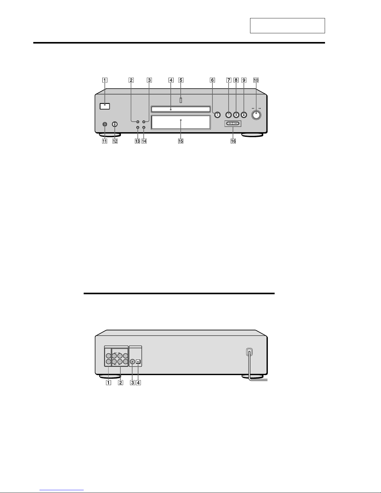
SCD-XB780
Front Panel Parts
Descriptions
Rear Panel Parts Descriptions
ANALOG
L
L
R
R
2CH OUT 5.1CH OUT OUT
FRONT COAXIAL OPTICALSURR CENTER
SUB
WOOFER
DIGITAL(CD)
1 ANALOG 2CH OUT L/R jacks
Connect to an audio component (stereo/2 channel)
using the audio connecting cord.
2 ANALOG 5.1CH OUT jacks
Connect to an amplifier equipped with the 5.1CH
input jacks (Multi-channel amplifier, AV amplifier,
etc.) using the audio connecting cords.
3 DIGITAL (CD) OUT COAXIAL connector
Connect to an audio component using the coaxial
digital cable.
4 DIGITAL (CD) OUT OPTICAL connector
Connect to an audio component using an optical
digital cable.
Note
Only the audio signals of the CD can be output from the
DIGITAL (CD) OUT connectors shown in 3 and 4. Those of the
Super Audio CD cannot be output through DIGITAL (CD) OUT.
SECTION 2
GENERAL
This section is extracted from
instruction manual.
PHONES
POWER
PHONE LEVEL
MIN MAX
PUSH ENTER
AMS
TIME/TEXT SACD/CD
MENU MULTI/2CH
OPEN CLOSE
1 POWER switch
Press to turn on the player.
2 TIME/TEXT button
Each time you press the button, the playing time of the
track, the total remaining time on the disc, or TEXT
information appears in the display.
3 SACD/CD button
Each time you press the button while playing back a
hybrid disc, the layer to be played back switches
between the HD (Super Audio CD) layer and the CD
layer.
4 Disc tray
Press A OPEN/CLOSE to open/close the disc tray.
5 Multi-channel indicator
Turns on when you turn on the player, or when the
Multi-channel Super Audio CD is loaded and select
the Multi-channel playback area by pressing MULTI/
2CH.
6 A OPEN/CLOSE button
Press to open the disc tray.
7 H button
Press to start play.
8 X button
Press to pause play.
9 x button
Press to stop play.
0 l AMS L dial (AMS: Automatic Music Sensor)
When you turn the l AMS L dial
counterclockwise by one click, you go back to the
preceding track; when you turn the l AMS L
dial clockwise by one click, you go to the succeeding
track.
qa PHONES
Connect the headphones.
During playback of a Multi-channel Super Audio CD,
the same signal that is output from the ANALOG
5.1CH FRONT L/R jacks is output from the PHONES
jack.
qs PHONE LEVEL
Adjust the headphones volume.
qd MENU
Press to enter the menu.
Press to exit from the menu and return to the normal
display.
qf MULTI/2CH button
Press to select the playback area when the 2 channel +
Multi-channel Super Audio CD is loaded.
qg Display window
Shows various information.
qh m/M buttons
Press to locate a portion you want to play within a
track.
7
SCD-XB780
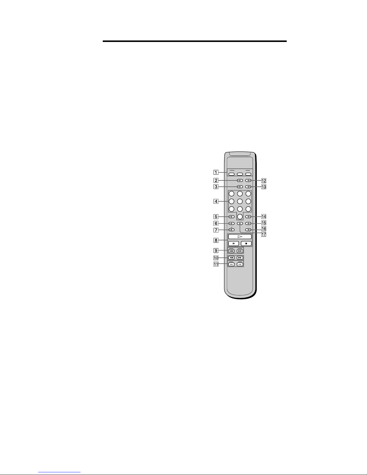
Remote Parts Descriptions
CONTINUE SHUFFLE
PLAY MODE
PROGRAM
SACD/CD
123
456
78
10/0
9
TIME/TEXT
REPEAT
AMS
BA
CLEAR
>10 ENTER
MODE
DISPLAY/
MULTI/2CH
INDEX
LEVEL
ADJ
CHECK
1 CONTINUE button
Press to resume normal play from Shuffle Play or
Programme Play.
SHUFFLE button
Press to select Shuffle Play.
PROGRAM button
Press to select Programme Play.
2 DISPLAY MODE button
Press to turn off the information.
3 TIME/TEXT button
Each time you press the button, the playing time of the
track, the total remaining time on the disc, or TEXT
information appears in the display.
4 Number buttons
Press to enter the track numbers.
5
i
10 button
Press to locate a track numbered over 10.
6 REPEAT button
Press repeatedly to play all tracks or only one track on
the disc.
7 A yB button
Press to select Repeat A-B Play.
8 H button
Press to start play.
X button
Press to pause play.
x button
Press to stop play.
9 AMS ./> (AMS: Automatic Music Sensor)
buttons
Press to locate a specific track.
0 m /M buttons
Press to locate a portion you want to play within a
track.
qa INDEX >/. buttons
Press to locate a specific point marked with an index
signal when you play a disc that has index signals.
qs SACD/CD button
Each time you press the button while playing back a
hybrid disc, the layer to be played back switches
between the HD (Super Audio CD) layer and the CD
layer.
qd MULTI/2CH button
Press to select the playback area when the 2 channel +
Multi-channel Super Audio CD is loaded.
qf ENTER button
Press to decide the selection.
qg CLEAR button
Press to delete a programmed track number.
qh LEVEL ADJ button
Press to adjust the output level balance for the Multichannel management function.
qj CHECK button
Press to check the programmed order.
SCD-XB780
8
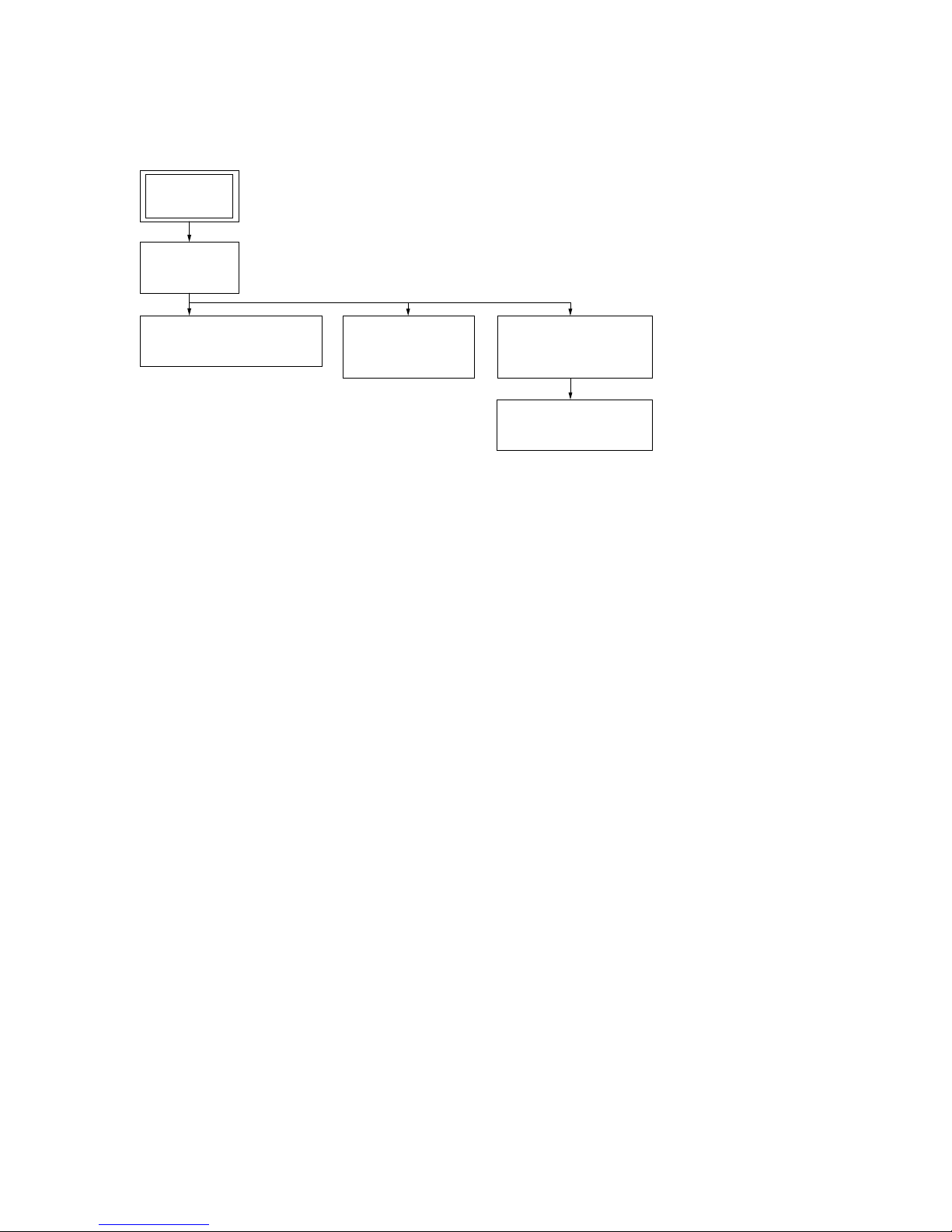
• This set can be disassembled in the order shown below.
3-1. DISASSEMBLY FLOW
SECTION 3
DISASSEMBLY
3-2. CASE
(Page 9)
3-3. FRONT PANEL SECTION
(Page 9)
3-6. BASE UNIT
(DVBU-6B)
(Page 11)
3-5. MECHANISM DECK
(CDM66B-DVBU6B)
(Page 10)
3-4. AUDIO BOARD,
MAIN BOARD
(Page 10)
SET
SCD-XB780
9
3-3. FRONT PANEL SECTION
Note: Follow the disassembly procedure in the numerical order given.
3-2. CASE
1
two screws
3
case
2
two flat head screws (TP)
2
two flat head screws (TP)
2
two flat head screws (TP
)
2
loading panel assy
1
Pull out the tray.
(Refer to page 3, HOW TO
OPEN THE TRA Y WHEN
POWER SWITCH TURNS
OFF.)
6
two claws
4
connector
(CN992)
7
front panel section
4
two connector
(CN305, 905)
3
wire (flat type)
(11 core)
(CN706)
6
two claws
5
six screws
(BV/RING)
SCD-XB780
10
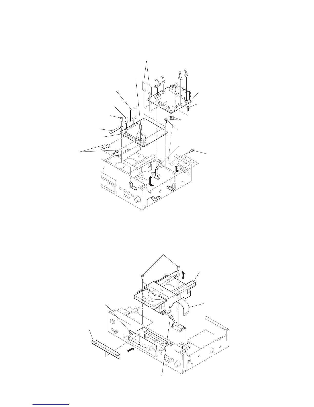
3-4. AUDIO BOARD, MAIN BOARD
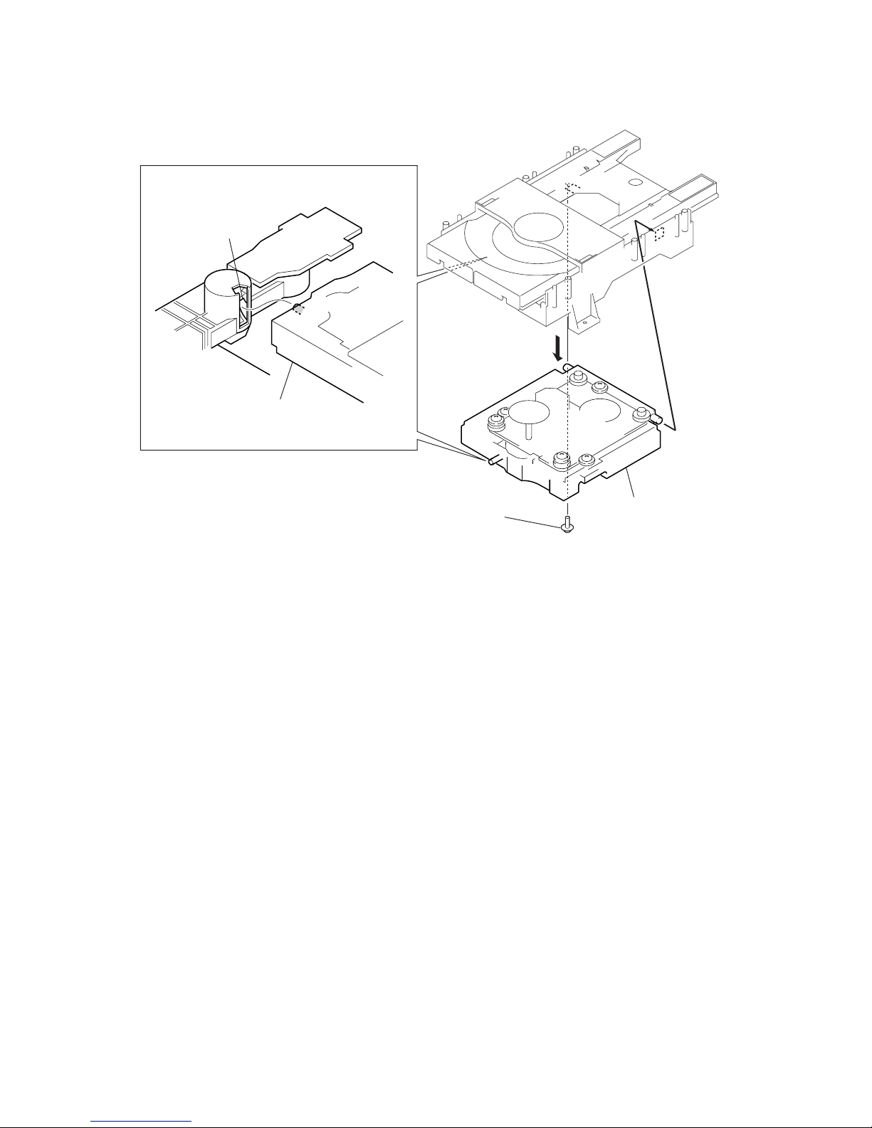
3-5. MECHANISM DECK (CDM66B-DVBU6B)
3
five screws
(BVT/RING)
2
four connectors
(CN301, 304, 305, 306)
1
two wires
(flat type) (19 core)
(CN302, 303)
7
AUDIO board
4
screw
(BVTT3
×
6)
5
two washers (DIA. 3.6)
0
three screws
(BVTT3
×
6)
6
PC board holder
8
wire (flat type)
(11 core) (CN706)
9
connector
(CN703)
0
screw
(BVTT3
×
6)
qs
MAIN board
qa
wiring stopper
9
two connectors
(CN704, 707)
8
wire (flat type)
(30 core) (CN708)
6
three screws
(BVTT3
×
8)
4
wire (flat type) (30 core
)
(CN708)
7
mechanism deck
(CDM66B-DVBU6B)
2
loading panel assy
5
connector (CN151)
1
Pull out the tray.
(Refer to page 3, HOW TO OPEN THE TRAY
WHEN POWER SWITCH TURNS OFF.)
3
Push
the tray.
SCD-XB780
11
3-6. BASE UNIT (DVBU-6B)
1
screw (DIA. 12), floating
2
– BOTTOM VIEW –
3
base unit (DVBU-6B
)
base unit (DVBU-6B)
cam (66)
12
SCD-XB780
Test Mode Command List
The contents of test mode are as follows.
Note: Wrong operation in the test mode causes a trouble, thus requiring extreme care.
LINE command (0X): Use mainly for a manufacturing line.
No. Name Description Remarks
00 RFAmp Read Each register set value of the IC001 (RF AMP) is displayed via RS-232C Not used for the servicing
05 DSP MON1 XUGF, XPCK, C2PO outputted from IC509 (CD DSP) Not used for the servicing
06 DSP MON2 MNT0, MNT1, MNT2, MNT3 outputted from IC509 (CD DSP) Not used for the servicing
07 DSP MON3 RFCK, XPCK, XROF, GTOP outputted from IC509 (CD DSP)
Electrical measurement,
CD CLV jitter measurement
STANDARD command (1X): Use when the servo is applied by manual operation.
No. Name Description Remarks
12 LD ON/OFF The laser diode is turned on or off On or off are switched alternately
13 SPIN ON/OFF The spindle motor is rotated with the regulated voltage On or off are switched alternately
14 FSRV ON/OFF The focus servo is turned on or off On or off are switched alternately
15 TSRV ON/OFF The tracking servo is turned on or off On or off are switched alternately
16 CLV ON/OFF
The spindle SLV servo is turned on or off
On or off are switched alternately
Focus and tracking servos must be already turned on
17 SSRV ON/OFF
The sled servo is turned on or off
On or off are switched alternately
Focus, tracking and spindle servos must be already turned on
18 ALL SRV ON All servos are turned on
19 ALL SRV OFF All servos are turned off Stop command in the test mode
FOCUS command (2X): Focus related. (All servos must be already turned on (except command 21))
No. Name Description Remarks
21 FSRCH ON/OFF
The continuous vertical motion of the optical pick-up lens is turned on or Avoid a long-time use
off On or off are switched alternately
22 F-BIAS UP Increase focus bias Focus bias value
23 F-BIAS DOWN Decrease focus bias Focus bias value
24 ADJ FCSBIAS
The focus bias is adjusted automatically
Both + and - directions are searched to search for best jitter point
25 FGAIN UP/DW The focus servo gain is switched between normal and down Normal or down are switched alternately
27 FOCUS AGC The focus servo gain is adjusted automatically
OFFSET (PI, FE, TE) command (3X): Adjusts the offset of PI, FE and TE signals.
No. Name Description Remarks
31 PI/FE OFSET
Adjusts the offset of PI, FE and TE signals TE offset adjustment is executed for the CD
This adjustment must be executed after 61 DISC DETECT only
SECTION 4
TEST MODE
In this set, various checks are automatically performed by executing
the commands in the test mode.
Note: This set makes adjustment e very optical pick-up and stores its result
in the EEPROM (IC903) on the MAIN board. Accordingly, if a
combination of optical pick-up and EEPROM is changed, be sure
to perform 4-3. SET CHECK. Also, perform 4-1. IC INTERFACE
CHECK, 4-2. DISPLA Y CHECK, and 4-6. WA VEFORMS CHECK.
Disc for Test Mode
Various checks of this set r equire the following discs.
Model Type *1 Category Application
MODEL
SATD-S5
12 cm disc
Adjusted value check,
(J-2501-215-A) SL
Reference disc
Operation check,
SATD-S4 Optical waveform check
(J-2501-184-A)
Not specified DL 12 cm disc Operation check
PATD-012
Adjusted value check,
(4-225-203-01)
CD
12 cm disc
Operation check,
YEDS-18 Reference disc
Optical waveform check
(3-702-101-01)
Not specified HYBRID 12 cm disc Operation check
*1 SL: Single Layer
DL: Dual Layer
Setting Method of Test Mode
Turn the
[POWER] button on while pressing the [ AMS ]
dial and the [MENU] button. Release the [MENU] button and the
[ AMS ] dial in this order when “DIAG MODE” is displayed
on the fluorescent indicator tube.
Releasing Method of Test Mode
To release the test mode, turn the [POWER] switch off.
Selection/Entry of Test Mode
To select and enter the “DIAG MODE”, operate as follows.
1. Rotate the [ AMS ] dial to select the menu, and press
the [ AMS ] dial to enter.
2. The test is switched on or off alternately each time the
[ AMS ] dial is pressed.
3. To return to the previous step, rotate the [ AMS ] dial
to select the desired item, and press the [ AMS ] dial
to enter.
lL
lL
lL
lL
lL
lL
l
L
13
SCD-XB780
TRACKING command (4X): Tracking servo related.
No. Name Description Remarks
41 TGAIN NM/UP The tracking servo gain is switched between normal and up Normal or up are switched alternately
44 ADJ TRK DSP The traverse AGC and E-F balance adjustment is performed
45 TRACKING AGC The tracking servo gain is adjusted automatically
SEARCH command (5X): Track search related. (Nos. 51 through 53 are not used for the servicing.)
No. Name Description Remarks
51 1-TRCK JUMP One-track jump is performed
52 FINE SEARCH Fine search is performed
53 M-TRCK MOVE M-track movement is performed
DISC DETECT command (6X): Disc type check related.
No. Name Description Remarks
Disc type check is executed
Display after judgment
61 DISC DETECT
DSKMOD CD: Judged as CD Refer to how to apply servo by manual
DSKMOD SL: Judged as SACD (SL) operation (See page 14)
DSKMOD DL: Judged as SACD (DL)
DSKMOD HYB: Judged as HYBRID
62 CD SETTING Enter disc type CD setting CD forced setting
63 SL SETTING Enter disc type SL setting SL forced setting
64 DL SETTING Enter disc type DL setting DL forced setting
6F Download Not used for the servicing
LASER command (7X): Laser of optical pick-up related.
No. Name Description Remarks
7A ADDTIME CD
Cumulative light emission time of the laser for CD is displayed
(Initialized by 8D command)
7B ADDTIME HD
Cumulative light emission time of the laser for SACD is displayed
(Initialized by 8D command)
7C FJUMP TEST Not used for the servicing
TOOLS command (8X): Performs aging, reads adjusting parameters, etc.
No. Name Description Remarks
81 VERSION Firmware version is displayed Example: Ver 1.00
83 TRAY AGING Tray open-close aging is performed Not used for the servicing
87 DISP ADJ DT Automatic adjusting parameters are displayed via RS-232C Not used for the servicing
8A FL CHECK Display of fluorescent indicator tube and keys are checked
8D SETUP MODE
Set to factory shipping mode Set when repair completed
PLAY MODE, etc. are initialized Refer to 4-5. SHIPPING MODE (See page 17)
QA command (9X)
No. Name Description Remarks
91 FJUMP CHECK The focus jump is checked Not used for the servicing
92 SET CHECK The set is checked Refer to 4-3. SET CHECK (See page 15)
93 WATER MARK Not used for the servicing
94 SET AGING
The set aging is performed
Not used for the servicing
Repeat by the specified number of times or until an error occurred
95 FJMP CHK BU The focus jump is checked (for jig) Not used for the servicing
9C BU DENCHO
The S curve waveform, traverse waveform, and RF waveform can be Refer to 4-6.WAVEFORMS CHECK
checked successively (See page 17)
9D PLAY&RFD ON
SACD playback, RFD output
Not used for the servicing
SACD jitter measuring mode
9E RFD ON/OFF
RFD output is turned on or off
Not used for the servicing
SACD jitter measuring mode
IC command (AX)
No. Name Description Remarks
A0 IC SELF CHK Each IC and its communication are checked Normal or up are switched alternately
14
SCD-XB780
How to Apply Servo by Manual Operation
In analyzing failures of the set, the servo may be applied by manual
operation. To apply servo in the test mode, use the following
method.
1. After setting the test mode, rotate the [ AMS ] dial to
select a command, and press the [ AMS ] dial to enter.
2. “61 DISC DETECT” (Disc type check)t“18 ALL SRV ON”
(All servos on + auto adjustment)
3. If applying servo while checking the condition one by one,
“61 DISC DETECT” (Disc type check)t“31 PI/FE OFSET”
(Offset automatic adjustment)t“14 FSRV ON/OFF” (Focus
servo on)t“16 CLV ON/OFF” (CLV servo on)t“44 ADJ
TRK DSP ” (E-F balance adjustment)t“15 TSRV ON/OFF”
(Tracking servo on)t“17 SSRV ON/OFF” (Sled servo
on)t“24 ADJ FCSBIAS” (Focus bias adjustment)t“27
FOCUS AGC” (Focus auto gain adjustment)t “45
TRACKING AGC” (Tracking auto gain adjustment).
Note: 1. On and off are alternately switched in the same command.
2. For a stop, select “19 ALL SR V OFF” and press the [ AMS ]
dial.
4-1. IC INTERFACE CHECK
The communication between microcomputer and main ICs is
checked.
Checking Method:
1. After setting the test mode, rotate the [ AMS ] dial to
select “A0. IC SELF CHECK” and press the [ AMS ]
dial to enter.
2. A checking will start automatically. (Checking time is about 3
seconds)
3. At successful completion of check, “IC CHECK OK” is displayed. In this case, no error exists in the IC interface.
Note: The check mentioned above tests the communication from micro-
computer to main ICs. Even if the check successfully finished, the
IC to be checked is not always normal. Consider it for reference
only.
4. In case of an IC communication error, the following display
will be given during the checking. Possible causes of error are
as listed below.
Error display Causes (typical example)
DVD DEC. ERROR 1. IC701 (SACD decoder) is faulty
2. IC701 pin <znv (XRST) does not go “H”
• IC901 pin ts (XDIS IO) does not go “H”
• IC904 (PLD) is faulty
3. 768fs (33.8688 MHz) is not present to
IC701 pin <znm (XTAL)
• IC811 (3-multiplying circuit) is faulty
• Clock signal 256fs is not sent from
AUDIO board (CN701 pin qg)
• CN702 pin 6 (GND) and pin 7
(+3.3V-D) are open or shorted
• CN701, 702 and FFC connection is loose,
or FFC is disconnected
DVD DRAM ERR 1. IC706 (D-RAM) is faulty
2. IC701 pin <znv (XRST) does not go “H”
• IC901 pin ts (XDIS IO) does not go “H”
• IC904 (PLD) is faulty
3. Faulty communication line between
IC701 and IC706
•Data line, address line, WE, etc.
4. D903 (1SS367) is faulty
D+3.3V is not present to IC706
CD DSP ERROR 1. IC509 (CD DSP) is faulty
2. 768fs (33.8688 MHz) is not present to
IC509 pin ua (XTAL)
Same as cause 3 of DVD DEC. ERROR
3. IC509 pin 2 (XRST) does not go “H”
• IC901 pin ts (XDIS IO) does not go “H”
• IC904 (PLD) is faulty
Error display Causes (typical example)
EEPROM ERROR 1. IC903 (EEPROM) is faulty
SAMBA DRAM ERR 1. IC808 (D-RAM) is faulty
(DSD decoder is also 2. IC801 (DSD decoder) is faulty
checked) 3. 768fs (33.8688 MHz) is not present to
IC801 pin qa (MCKI)
Same as cause 3 of DVD DEC. ERROR
4. IC801 pin 9 (XRST) does not go “H”
• IC901 pin ts (XDIS IO) does not go “H”
• IC904 (PLD) is faulty
5. Faulty communication line between
IC801 and IC808
•Data line, address line, WE, etc.
6. D904 (1SS367) is faulty
D+3.3V is not present to IC808
RF AMP ERROR 1. IC001 (RF AMP) is faulty
2. Loose connection between CN708 on
MAIN board and CN005 on RF board,
or FFC disconnection
CN708 pin qj (CLK RF), pin qh (DATA
RF) and pin qg (SDEN) must be checked
SD BUS ERROR 1. IC701 SD bus and IC801 AV decoder
interface is faulty
2. IC812 to 814 are faulty
Causes Common to Each IC:
1. Faulty communication line between microcomputer and each
IC.
Disconnected patterns, floating series resistors, bridge, etc.
2. Faulty IC supply voltage.
Particularly, check D+3.3V voltage.
3. Faulty microcomputer communication port to each IC
Note: In case of more than two errors, the error display is switched over
one after another, thus making the reading difficult.
In such a case, press again the [ AMS ] dial to make a
recheck for error reading.
4-2. DISPLAY CHECK
Checking Method:
1. After setting the test mode, rotate the [ AMS ] dial to
select “8A. FL CHECK” and press the [ AMS ] dial to
enter.
2. Respective segments of fluorescent indicator tube will
automatically light up in order, and therefore check that there
is no chipped character.
3. The “INPUT REMOCON” will be displayed after the segment
check finished successfully, and then press a proper key on
the remote commander.
4. After “JOG CHECK” is displayed, the numbers of calendar
will be displayed from 1 to 15 each time the [ AMS ]
dial is rotated clockwise.
5. After display up to 15, the numbers of calendar will
disappear in order each time the [ AMS ] dial is
rotated counterclockwise.
6. “TTX-1514?” will be displayed when all are cleared, and then
press the [ AMS ] dial.
7. Upon display of “KEY CHECK”, if a key on the display is
pressed, the corresponding segment of fluorescent indicator
tube will light up.
8. “FL TEST END” will be displayed if all keys are pressed.
Note: The keys include the [ AMS ] dial. If the segment that
corresponds to the pressed key does not light up, that key is faulty.
9. The test mode selection display will be back, if the [ AMS ]
dial is pressed.
lL
lL
lL
lL
lL
lL
lL
lL
lL
lL
lL
l
L
lL

15
SCD-XB780
4-3. SET CHECK (AUTOMATIC VARIOUS MEASUREMENTS)
The operational stability of the set is checked. The check and OK/NG judgment are performed automatically.
Note: In the set check using the CD, besides a checking, the MIRR time used for the disc check is measured every optical pick-up, and from the measured
result, the threshold value is calculated and it is stored in the EEPROM (IC903) on the MAIN board. Accordingly, if a combination of optical pickup and EEPROM is changed (for example, the optical pick-up or MAIN board is replaced), be sure to perform the set check using the following CD.
As the data stored in the EEPROM are overwritten every set check, retry if failed. For the set check using the SACD, only checking is made.
Set Check
CD and SACD (SL) Disc Operation Check
Checking method:
1. After setting the test mode, rotate the [ AMS ] dial to select “SET CHECK” and press the [ AMS ] dial to enter.
2. Upon display of “AUTO CHECK SP?”, further press the [ AMS ] dial.
3. The tray will open automatically, and then set the test disc*1 of CD or SACD.
4. With the “DISC IN&JOG ON” displayed, press the [ AMS ] dial, and the check will be executed automatically.
5. “SPEC OK!” will be displayed if the measured result is within the specification. Faulty item name and the measured result will be
displayed if any measured item is NG.
6. After that, “A UT O CHECK SP?” will be again displayed, and then rotate the [ AMS ] dial to select “CHECK END?”. Further,
press the [ AMS ] dial, and the test mode selection display will be back, and then press the [OPEN/CLOSE ] button and take
the test disc out.
*1 Use PATD-012 or YEDS-18 for CD, and SATD-S5 or SATD-S4 for SACD (SL). Using another disc will result in a checking failure.
Measured Items:
Items Description Remarks
Offset values before RF (PI), VC, FE, TE signal offset adjustment At offset 0
RF/VC/FE/TE (ORG) RF (8 bit data in hex notation) RF: A0h
VC, FE, TE (9 bit data in hex notation) VC, FE, TE: 00h
Offset values after RF (PI), VC, FE, TE signal offset adjustment VC offset is not adjusted
RF/VC/FE/TE (ADJ)
(Less than ORG value if offset correction is normal) (Measurement only)
RF (8 bit data in hex notation) Also, for SACD, the TE offset is
VC, FE, TE (9 bit data in hex notation) not measured and adjusted
PI (ORG): PI value at disc type check (decimal data) PI level conversion
PI (ADJ): PI value after PI offset adjustment Read value × 12.9mV
(read value at microcomputer A/D) (decimal data)
PI/TRVS PP (ORG/ADJ) TRVS PP (ORG): Traverse level before level correction (AGC) Traverse level conversion
(decimal data) Read value × 12.9mV
TRVS PP (ADJ):Traverse level after level correction (AGC)
(decimal data) 12.9mV=3.3V ÷ 256 (8 bit)
PIOR: Set value of PI offset coarse adjusting register Registers in RF amplifier
PIOR/CCR/TRCR CCR: Set value of FE offset coarse adjusting register
TRCR: Set value of TE offset coarse adjusting register
FOCUS/TRK GAIN
Auto gain adjusted values of focus and tracking servos
(8 bit data in hex notation)
FBIAS: Focus bias set value (9 bit data in hex notation)
TRCR2 adjusts the E-F gain
TRVSC: Traverse center value (9 bit data in hex notation)
balance and used for CD only
FBIAS/TRVSC/TRCR2/CFR
TRCR2: Set value of E-F balance coarse adjusting register
(Fixed to 06 for SACD)
CFR: Set value of traverse level adjusting register
TRCR2 and CFR are registers in
RF amplifier
PSP AMPLITUDE SACD only
1-LAST TRK SEEK (msec) Average seek time from first track to last track of disc
Error rate measurement
For the CD, Measure for 7 sec at track
ERROR RATE For CD: Average value/Maximum value of C1 and C2
No.5
For SACD: Average value/Maximum value of PO, PI1 and PI2
For the SACD, calculation from 100-
block data at track No.5
lL
A
92. SET CHECK AUTO CHECK SP?
AUTO CHECK?
DISP RESULT S?
CHECH END?
DISP RESULT F?
The set check is executed to judge OK or NG.
(For the CD, the threshold value is stored in the EEPROM)
The measured result is displayed on the fluorescent indicator tube.
The set check of measurement only is executed.
The measured result is displayed via RS-232C.
The set check is finished.
lL
lL
lL
lL
lL
16
SCD-XB780
Measured Items Specified value
RF AVRG (ADJ) 8Ch to ABh
VC AVRG (ADJ) 1F7h to09h
FE AVRG (ADJ)
(1) CD 1EEh to 12h
(2) SACD 1F1h to 0Fh
TE AVRG (ADJ) 1E2h to 1Eh
TRVS PP (ADJ) 45h to 73h
FCS GAIN 10h to 60h
TRK GAIN 10h to 60h
(1) CD
C1 20 or less
ERROR RATE C2 0
(2) SACD
PI1 NUM 100 or less
PI1 FRAME 5 or less
PSP AMPLITUDE (SACD only) 1000 to 4000
1-LAST TRK SEK 3500 or less
Hexadecimal (hex) display 9 bit data
FF 011111111 (+255)
FE 011111110 (+254)
(+) Side
(-) Side
MAX
01 000000001 (+1)
00 000000000 (0)
1FF 111111111 (-1)
101 100000001 (-255)
100 100000000 (-256)
Hexadecimal (hex) display 8 bit data
7F 01111111 (+127)
7E 01111110 (+126)
01 00000001 (+1)
00 00000000 (0)
02 00000010 (+2)
FF 11111111 (-1)
FE 11111110 (-2)
81 10000001 (-127)
80 10000000 (-128)
MIN
0
Specified Value:
Specified value used for OK/NG judgment when executing 92. SET CHECKtAUTO CHECK SP?
Note: The specified values attached with “h” are hexadecimal n umbers, and others are decimal numbers.
RF, VC, FE, and TE measured values are hexadecimal data with positive and negative signs. When comparing the measured
value with the specified value, refer to the following.
17
SCD-XB780
4-4. SACD (DL) DISC OPERATION CHECK
(• Perform as necessary)
This checking performs the focus jump using a DL disc, which is
a dual-layer HD disc, to verify the stability of the set.
A set of layer 0 most-outside track access (only once)tone-second
tracetfocus jump (layer 0t1)tone-second tracetfocus jump
(layer 1t0) are repeated 5 times.
Checking Method:
1. After setting the test mode, rotate the [ AMS ] dial to
select “91 FJUMP CHECK” and press the [ AMS ] dial
to enter.
2. The tray will open automatically, and then set the DL disc.
3. With “DISC IN&JOG ON” displayed, press the [ AMS ]
dial.
4. The tray will be loaded in automatically, and then the test will
start.
5. During the test, “NOW TESTiiii” is displayed.
6. Upon successful completion of the check, “OK!” will be
displayed and the tray will open automatically. (In case of
NG, “NG! ERR FJ-UP” or “NG! ERR FJ-DWN” is displayed)
7. Take the DL disc out and press the [OPEN/CLOSE ] button,
and the test mode selection display will be back
4-5. SHIPPING MODE
The repaired set must be initialized, and for this purpose the set
should be set to the shipping mode.
Setting Method:
1. After setting the test mode, rotate the [ AMS ] dial to
select “8D SETUP MODE” and press the [ AMS ] dial
to enter.
2. “INITIAL OK” is displayed and the test mode selection display
will be back immediately.
“8D 000000000 00” will be displayed, and if the scroll starts in
the left direction, the set initialization has completed
3. Press the
[POWER] button to turn the power off.
The following setups are established in the shipping mode
1. Initialization of EEPROM (IC903)
• PLAY MODE CONTINUE
• LAYER SELECT SACD
• M/2CH SELECT MULTI
• 2ch SPK MODE 2ch DIRECT
• Mch SPK MODE Mch DIRECT
• Resetting the cumulative light emission time of the laser
Note: Even if the shipment mode setting mentioned above is made, the
disc check threshold value attained in the 3. SET CHECK is not
cleared.
2. The optical pick-up moves to the home position (most-inside
track)
Error List
Display Description
Toc Error * Error during the time from auto adjustment to TOC
reading, Different type of disc (Such as a DVD disc),
Disc is dirty
Toc Error **** Illegal SACD (Such as a pirated version)
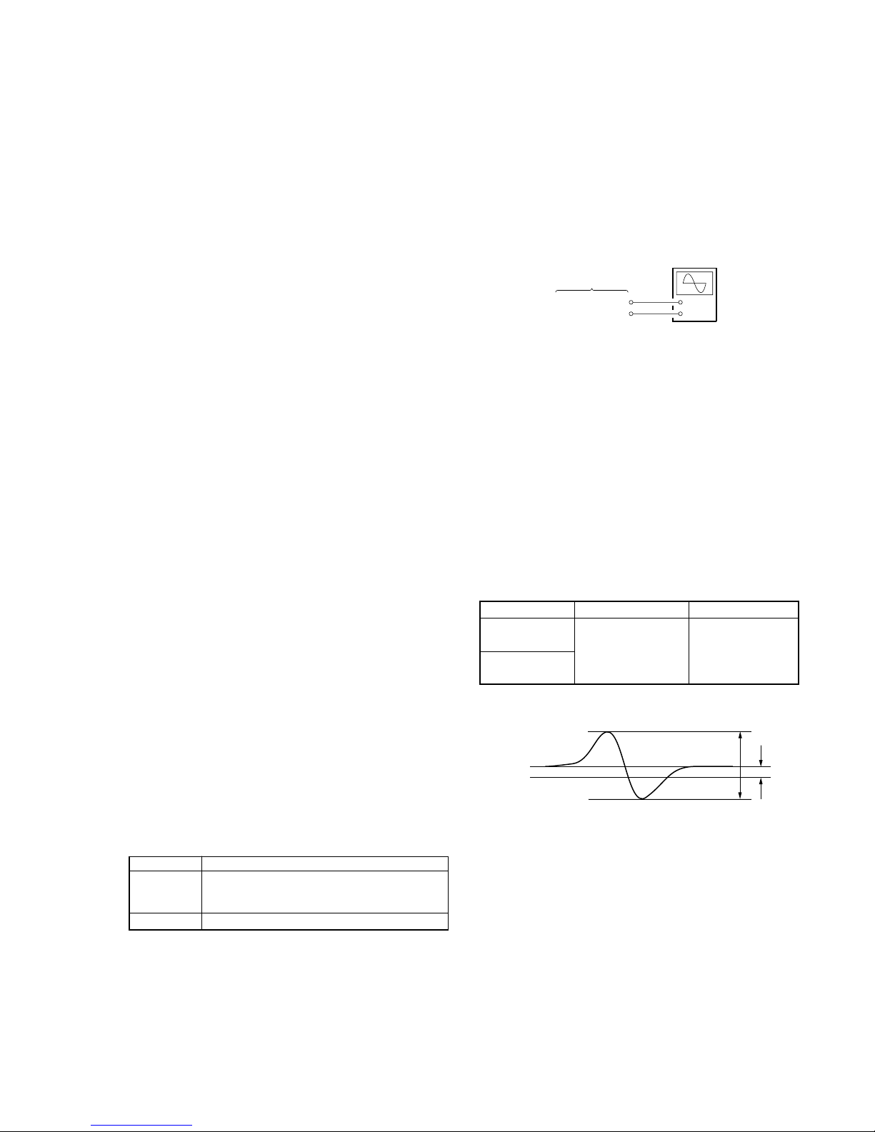
4-6. WAVEFORMS CHECK
BU Electrical Adjustment Mode
The BU electrical adjustment mode is used to check the S curve
waveform, traverse waveform, RF wav eform, and CL V jitter . After
a disc is placed on the tray, each time the [ AMS ] dial is
pressed, the check mode is switched in order for S curve
waveformt tra verse wav eformtRF waveformtCLV jitter (for
the CD).
S Curve Check
Connection:
Checking Method:
1. After setting the test mode, rotate the [ AMS ] dial to
select “9C. BU DENCHO” and press the [OPEN/CLOSE ]
button. Place the test disc (PATD-012 or YEDS-18 or SATDS5 or SATD-S4) on the tray and close the tray, then press
the [ AMS ] dial.
2. At the completion of disc type check, “CD DETECT” will be
displayed (for PATD-012 or YEDS-18).
Note: For the SATD-S5 or SATD-S4, “SL DETECT” is displayed.
3. Press again the [ AMS ] dial, and the S curve waveform
check mode will become active and “S-CURVE MODE” will
be displayed.
4. Connect an oscilloscope to the TP506 (FE) and TP504 (AVC)
on the MAIN board.
5. Check that the level A and B of wa veform on the oscilloscope
satisfy the specification.
Specified Value:
Disc AB
SATD-S5 or
SATD-S4
PATD-012 or
0.7 to 1.7 Vp-p –0.1 to +0.1V
YEDS-18
Note: For easier observation of this waveform, extend the sweep time
and raise the brightness.
Checking and Connecting Location : See page 19.
MAIN board
TP506 (FE)
TP504 (AVC)
+
–
oscilloscop
e
A
B
S curve waveform
VC
lL
l
L
lL
lL
lL
lL
A
A
lL
lL
lL
18
SCD-XB780
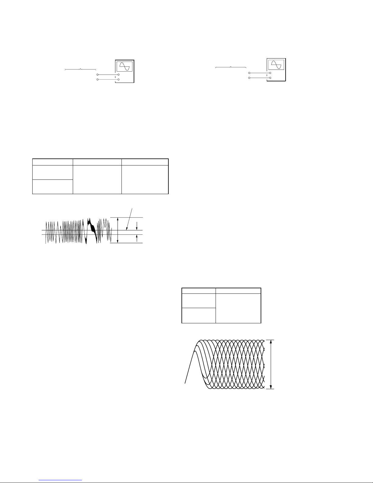
RF Level Check
Connection:
Checking Method:
1. Under the condition of traverse waveform check mode in step
4, press the [ AMS ] dial.
2. Connect an oscilloscope to the TP703 (RFAC) and TP704
(AGND) on the MAIN board.
3. After “W AIT” is displayed, the RF waveform check mode will
become active and “PLAY 5th TRACK” (for the SA CD, “RF
MODE ON”) will be displayed, and the 5th music on the disc
will be played.
4. Check that the RF waveform is clear and the level satisfies the
specification.
5. Press the [ AMS ] dial (for the SACD, “RF JITTER
(5th)” will be displayed, and further press the AMS dial), and
“OUTSIDE TRACK” will be displayed and the outward track
of the disc will be played.
6. Check that the RF waveform is clear and the level satisfies the
specification.
7. Press the [ AMS ] dial, and “INSIDE TRACK” will be
displayed and the inward track of the disc will be played.
8. Check that the RF waveform is clear and the level satisfies the
specification.
9. After checking, press the [ AMS ] dial, and the test is
over when “BU MEASURE” is displayed.
10. Press the [OPEN/CLOSE ] button to open the tray, and remove the test disc.
11. Using each type of disc, repeat from step 1 of S curve waveform check up to step 10 of RF level check.
12. When the check is over, press the
[POWER] button to turn the
power off.
Note: Take care not to leave the test disc in the set.
Specified Value:
Disc A
SATD-S5 or
SATD-S4
PATD-012 or
0.9 to 1.4 Vp-p
YEDS-18
Note: Clear RF waveform refers to the wav eform where ◊ shapes should
be distinctively observed in the center.
Checking and Connecting Location : See page 19.
MAIN board
TP703 (RFAC)
TP704 (AGND)
+
–
oscilloscope
VOLT/DIV: 200 m
V
TIME/DIV: 500 ns
RF signal waveform
A
lL
lL
lL
lL
A
Traverse Check
Connection:
Checking Method:
1. Under the condition of S curve waveform check mode in step
5, press the [ AMS ] dial.
2. After “W AIT” is displayed, the traverse wa veform check mode
will become active and “TRV MODE ON” will be displayed.
3. Connect an oscilloscope to the TP513 (TE) and TP504 (AVC)
on the MAIN board.
4. Check that the level A and B of waveform on the oscillo-
scope satisfy the specification.
Specified Value:
Disc AB
SATD-S5 or
SATD-S4
PATD-012 or
0.9 to 1.4 Vp-p –0.1 to +0.1V
YEDS-18
Checking and Connecting Location : See page 19.
MAIN board
TP513 (TE)
TP504 (AVC)
+
–
oscilloscope
A
B
VC
Center fo the waveform
Traverse waveform
lL
SCD-XB780
1919
– MAIN Board (Component Side) –
TP506
(FE)
TP513
(TE)
TP504
(AVC)
TP704
(AGND)
TP703
(RFAC)
TP514
(RFCK)
TP517
(WFCK)
TP808 (DG)
IC703
IC701
IC509
IC801
CLV Jitter Check (CD only)
Connection:
Checking Method:
Under the condition of RF level check mode in step 3, connect the
oscilloscope to the TP516 (RFCK) (CH1), TP517 (WFCK) (CH2),
and the TP808 (DG) (GND) on the MAIN board to check that the
value A of the waveform satisfies the specification.
Note: Take care not to leave the test disc in the set.
Specified Value:
Disc A
PATD-012 or
35 µsec or less
YEDS-18
Checking and Connecting Location:
A
CLV jitter waveform
MAIN board
TP516 (RFCK)
TP517(WFCK)
TP808 (DG)
+
+
–
oscilloscop
e
(CH2)
(CH1)
SCD-XB780
2020
SECTION 5
DIAGRAMS
5-1. BLOCK DIAGRAM – RF/SERVO Section –
MUTE LOAD
DETECTOR
1
63
3
4
5
6
9
10
11
12
14
15
16
13
18
17
61
62
535254
55
59
60
DVDRFP
RFSIN
A2
B2
C2
D2
CD E
CD F
A
B
C
D
A
B
C
D
A
B
C
D
A
B
C
D
CD A
CD B
CD C
CD D
DVDLD
CDPD
CDLD
DVDPD
DVDPDSW
MUX ATT
ATON
ATOP
FNP
FNN
INPUT
BIAS,
AGC
PROGRAMMABLE
EQ FILTER
DIFFERENTIATOR
AIP
AIN
DIP
DIN
SUMMING AMP
IC004 (1/4)
SUMMING AMP
IC004 (2/4)
GCA
MUX
DUAL
APC
GCA,
EQ
GCA
L. P. F.
+
–
PHASE
DETECTOR
COMPARATOR MUX
+
–
+
–
+
+
+
+
+
+
+
–
CLAMP&
ENVELOPE
LEVEL DAC
GCA
SUB GCA
SEL
L. P. F.
OFFSET
CANCEL
MUX
BOTTOM
ENVELOPE
INPUT
BUFFER
PEAK/
BOTTOM
HOLD
SERIAL
PORT
REGISTER
57
27
31
32
39
47
46
48
FULL WAVE
RECTIFER
AGC
CHARGE PUMP
AVC BUFFER
IC004 (4/4)
AVC
(+1.65V)
A+3.3V
WAVRB BUFFER
IC503 (1/2)
WAVRB
D+5V
VC
(+2.5V)
VC
AGCO
SACD/CD RF AMP,
FOCUS/TRACKING ERROR AMP
IC001
OPTICAL PICK-UP
BLOCK
(KHM-234AMA)
MODULE
CIRCUIT
2AXIS
DEVICE
FOCUS/
TRACKING
COIL
21
22
23
12 5
11 6
9
AUTOMATIC POWER
CONTROL (FOR CD)
Q003
AUTOMATIC POWER
CONTROL (FOR SACD)
Q001
FOCUS COIL
DRIVE
14 2
13 3
TRACKING COIL
DRIVE
17 24
18 23
33
34
20
22
21
19
8
40 41 39 43
31
32
29
30
20
SLED MOTOR
DRIVE
FOCUS/TRACKING COIL DRIVE,
SLED MOTOR DRIVE
IC502
M
M2
(SLED)
8
9
SPINDLE MOTOR
DRIVE
MM
M3
(SPINDLE)
6
5
LOADING MOTOR
DRIVE
MM
M151
(LOADING)
16 17
13
FOCUS/TRACKING/SLED
PWM GENERATOR
FFDR
FRDR
TFDR
TRDR
SFDR
SRDR
SERVO
INTERFACE
SERVO AUTO
SEQUENCER
A/D
CONVERTER
FOCUS
TRACKING/SLED
SERVO DSP
DFCT, FOK
DETECTOR
26
SE
TE
FE
RFDC
TE
FE
PI
26
DIGITAL SERVO
PROCESSOR
IC509 (1/2)
TO CPU INTERFACE
D+3.3V
S1
(LIMIT)
MIRR
FOK
DFCT
COUT
SCLK
SSTP
STBY1
STBY2
RF
A
B
C
D
E
F
G
H
DVD LD
CD LD
DVD/CD PD
DVD VR
FCS+
FCS–
TRK+
TRK–
D
CBA
AGCO
RFAC
MIRR
MIN
MEVO
PI
FE
TE TE
SDATA
SCLK
SDEN
LDON
LOAD OUT
LOAD IN
MUTE 2D
SPDA
F JMP1
F JMP2
• SIGNAL PATH
: SACD PLAY
: CD PLAY
2
RFAC
(Page 21)
3
TE, FE, PI
(Page 22)
4
SDATA, SCLK, SDEN
(Page 22)
5
LDON
(Page 21)
DVDPDSW, CDPDSW
(Page 22)
10
SPDA, F JMP1/2
(Page 21)
11
SPIN
(Page 21)
12
MUTE 2D, SP ON, MUTE LOAD
(Page 22)
13
LOAD IN/OUT
(Page 22)
8
FOK, MIRR,
COUT, SCLK
(Page 22)
TRKSW
(Page 22)
DRVC BUFFER
IC503 (2/2)
DRVC
(+2.5V)
D+5V
SPINDLE MOTOR
DRIVE
42MNTR
FE
PI
PIFETE
SDATA
SCLK
SDEN
MIRR
FOK
COUT
SCLK
9
(Page 22)
LIM SW
BUFFER
BUFFER
2
SP ON
MUTE2
MUTE1
SPINDLE/LOADING MOTOR DRIVE
IC512
21
22
24
15
23
L. P. F.
GCA
OFFSET
CANCEL
40
L. P. F.
OFFSET
CANCEL
38
PI ERROR AMP
IC004 (3/4)
24
PHOTO DIODE
CONTROL SWITCH
(FOR SACD)
Q005
CD VR
PHOTO DIODE
CONTROL SWITCH
(FOR CD)
Q004
TRACKING COIL DRIVE
CONTROL SWITCH
IC501
1 241 2
CDPDSW
7
6
TRACKING COIL DRIVE
CONTROL SWITCH
IC505
27
26
1
(Page 21)
SP ERR
25
4
SCD-XB780
2121
53 55 52 54 12
50
49
48
24
75
100
25 4 6 5 7 15 79 80 76 77 10 11 13
34 35 36 9 26 33 37 71
3
2
138
68
64
17
14
65
67
66
71
72
6916
43 44 64 58 85 84 12 22 23
117
111
7 8
89 – 96 14 – 21
A0 – A7 D0 – D7
142
144
140
135
147148150151137 153 146 155 163 158 160 164
26
46
51
54
62
63
49
48
53
23
162
29
44, 41, 39, 35,
32, 30, 27, 24
31, 34, 37,
40, 43, 45
59, 56, 60
157159939294767895
3334
170
171835
21 – 24, 27 – 32
79, 80, 82 – 87,
89, 91
41 – 44, 46 – 49
96, 97, 99, 101,
102, 104 – 106
2 – 5, 7 – 10
5, 7, 9 – 14 172 – 176, 1, 2, 4
66 – 69, 71,
73 – 75
169167
109
107
16
21
20
19
18
17
113 114 115
2
FILTER
ASYMMETRY
CORRECTOR
EFM
DEMODULATOR
32K
RAM
D/A
DIGITAL
INTERFACE
CLOCK
GENERATOR
ERROR
CORRECTOR
DIGITAL
OUT
SUBCODE
PROCESSOR
DIGITAL CLV
PROCESSOR
CPU INTERFACE
DIGITAL PLL
INTERNAL BUS
C4M
XTSL
DIGITAL SIGNAL
PROCESSOR
IC509 (2/2)
RFAC
RFAC
ASYI
ASYO
FILO
PCO
XPCK
FILI
CLTV
D+3.3V
XTAO
XTAI
PCMD
WDCK
DOUT
XRST
C2PO
LRCK
BCK
MDAT
LRCK
BCLK
XRST DVD
WAVE SHAPER
Q302
OPTICAL
TRANSCEIVER
IC309
18
17
19
20
DIGITAL (CD)
OUT OPTICAL
DIGITAL (CD)
OUT COAXIAL
J303
(Page 22)
(Page 22)
(Page 23)
(Page 22)
21
(Page 22)
SD0 – SD7
SDEF
22
(Page 22)
23
(Page 22)
24
(Page 22)
25
(Page 22)
RFAC
768FS (33.8688MHz)
MDAT, BCLK, LRCK
XRST CD, MUTE CD, XRST DVD
HOST INTERFACE
DLRC
DDAT
MA10/MNT1
XMOE
XCAS
MA0 – MA9
MDB8, MDB9,
MDBA – MDBF
MDB0 – MDB7
DASYO
DASYI
ASF1
ASF2
XRAS
XMWR
MA11/MNT2
DBCK
XSAK,
XSHD,
XDCK,
XSRQ
WPK
XTAL
HDB0 –
HDB7
HDB8
HDB9
HDBA –
HDBF
HA0 –
HA2
XSAK
XHRS
XSRQ
XDCK
XSHD
HCS1
HCS0
HINT
REDY
• SIGNAL PATH
: SACD PLAY
: CD PLAY (ANALOG)
: CD PLAY (DIGITAL OUT)
ATAPI
PACKET FIFO
ATAPI
REGISTER
DMA
FIFO
DAC
INTERFACE
CD ESP
OE
UCAS
WE
RAS
LCAS
A0 – A9I/O8 – I/O15I/O0 – I/O7
D-RAM
IC706
AUTHENTICATION
CPU
INTERFACE,
DMA
CONTROLLER
XTL1
XTL2
XTAL
APEO
GFS
XWAIT
XRD
XWR
XCS
XINT0
XINT1
DATA BUS
ADDRESS BUS
DATA BUS
ADDRESS BUS
INTEGRATOR
IC703 (1/2)
16
(Page 22)
15
(Page 22)
14
(Page 22)
10
(Page 20)
5
(Page 20)
XHRD, XHWR
A0
D0 – D7
SPDA, F JMP1/2
LDON
11
(Page 20)
SPIN
F JMP1
SPDA
F JMP2
TO SERVO AUTO
SEQUENCER
LOCK
MDP
DATA
SQCK
WFCK
EMPH
MUTE
GFS
RFCK
SQSO
EXCK
SBSO
SCOR
SENS
XLAT
CLOK
LOCK CD
DATA CD
CLOK CD
XLAT CD
SENS CD
SCOR CD
SQSO CD
SQCK CD
GFS CD
3
DOCTRL
LD ON
SPDA
APDO
JITTER
GFS DVD
XRD
XWR
XCS DVD
INIT0 DVD
INIT1 DVD
XHRD
XHWR
XCS
XINT0
XINT1
FCS JMP1
FCS JMP2
SPINDLE MOTOR DRIVE
IC708 (2/2)
SYNC
CONTROL
SUBCODE
DEINTERLEAVE & ECC
DESCRAMBLE
BUFFER
IC708 (1/2)
FFM
DEMODULATOR
RF
ASSYMMETRY
PLL
FILTER
ANALOG
MIXER
SPINDLE
CONRTOL
CD DSP INTERFACE
MDSOUT
MDIN1
MDPOUT
CLVS
SPO
MDIN2
WFCK
SCOR
SBIN
EXCK
XRCI
GSCOR
C2PO
LRCK
BCLK
MDAT
XRST
WFCK
SCOR
SBSO
EXCK
A0 – A7
D0 – D7
SACD DECODER
IC701
RFIN
CPU
IC901 (1/3)
63
MD2
MAIN DATA ECC & EDC
DVD-ROM CD-ROM
59
1
(Page 20)
SP ERR
SP ERR
DMA CONTROLLER
(PRIORITY RESOLVE & SEQUENCER)
(Page 20)
XRST CD
MUTE CD
XHRD
XHWR
XCS
XINT0
XINT1
XSAK
XSRQ
XDCK
XSHD
DVC BUFFER
IC703 (2/2)
DVC
(+1.65V)
A+3.3V
5-2. BLOCK DIAGRAM – SERVO Section –
SCD-XB780
2222
5-3. BLOCK DIAGRAM – MAIN Section –
11 – 18
DQ0 – DQ7
169 – 176
2 – 9
B1 –
B8
A1 –
A8
2 18
3 17
4
5 15
16
64
LEVEL SHIFT
IC814
164
11 12
11
2
13 1
3
16
17
15
34
D-RAM
IC808
LEVEL SHIFT
IC813
LEVEL SHIFT
IC812
DSD DECODER
IC801
3-MULTIPLYING
IC811
21
(Page 21)
3
(Page 20)
8
(Page 20)
4
(Page 20)
22
(Page 21)
23
(Page 21)
24
(Page 21)
17
(Page 21)
25
(Page 21)
18
(Page 21)
20
(Page 21)
74
83
77
74
25
29
72
65
67
SDATA
SDEN
SCLK
FOK
MIRR
COUT
SCLK
TE
FE
10 4
9 5
8
6
6
4
3
2
10
7
48
49
50
47
51
27
11
52
35
78
79
38
EEPROM
IC903
5
6
SDA
SCL
RESET SIGNAL
GENERATOR
IC905
9
10
11
24
25
31
32
768FS (33.8688MHz)
XTAL
XSAK
XSHD
XDCK
XSRQ
SDEF
SD0 – SD7
SDATA, SCLK, SDEN
FOK, MIRR, COUT, SCLK
TE, FE, PI
XRST CD, MUTE CD, XRST DVD
12 – 16, 19 – 21
DATA BUS
27
(Page 23)
14
(Page 21)
15
(Page 21)
16
(Page 21)
45
46
13
(Page 20)
• SIGNAL PATH
: SACD PLAY
A1
A2
A3
B1
B2
B3
A4
B4
A0 – A11
CAS
RAS
WE
CKE
DQ0 – DQ7A0 – A11
SD0 – SD7
SDCK
SDEF
XSAK
XSHD
XSRQ
WCK
XCAS
XRAS
XWE
DCKE
DSAL
MCKI
DSALS
MSDATO
MSDATI
MSCK
XMSLAT
SMUTE
MSREADY
SDATAL
SDATALS
DATA RF
CLK RF
FOK CD
MIRR RF
COUT CD
SCLK CD
TE
FE
SIN DSD
SOUT DSD
SCK DSD
XLAT DSD
MUTE DSD
RDY DSD
CPU
IC901 (2/3)
XCS IO
XDIS IO
EEPSIO
EEPSCL
XRST
SDEN
XCS
RST
RST DSD
RST DVD
RST CD
XRD
XWR
D0 – D7
LOAD IN
LOAD OUT
PROGRAMMABLE
LOGIC DEVICE
IC904
XRST CD
SDATAL, SDATAR, SDATALS, SDATARS,
SDATAC, SDATALF, 64FS
D0 – D7
A0
XHRD, XHWR
LOAD IN/OUT
66PIPI
98
97
LATCH DF
INIT DF
22A
166
165
167
168
XASK, XSHD,
XDCK, XSRQ
126 WARFI
REAC
WPK
2, 3, 5, 6,
8, 9, 11, 12
139 – 136,
134 – 131
21 – 24, 27 – 32,
20, 19
162 – 159, 157 – 154,
152, 151, 149, 148
144
145
143
142
35CLK DCLK
141
66DSAR
SDATAR
76DSARS
SDATARS
69DSAC
SDATAC
71DSASW
SDATALF
61PHREFI
64FS
59BCKAI
128FS
26
(Page 23)
34MULTI
30
(Page 23)
3
4
FS64
FS128
5YO
64FS
128FS
XHRD
XHWR
2
41
28
(Page 23)
ZEROL
ZEROR
ZEROL, ZEROR
ZEROL
ZEROR
38
37
29
(Page 23)
LMUTE
RMUTE
LMUTE, RMUTE
LMUTE
RMUTE
33
23
6
(Page 20)
DVDPDSW
CDPDSW
DVDPDSW, CDPDSW
DVDPDSW
CDPDSW
LOAD IN
LOAD OUT
40 XTAL
41 EXTAL
X901
20MHz
DATA
CLK
LATCH
INIT
32
(Page 23)
DATA, CLK,
LATCH, INIT
26
31
(Page 24)
RST DP
XRST DP
36 ISBTEST
12
(Page 20)
MUTE 2D, SP ON, MUTE LOAD
115
TEST1
XRST
9
43 ZDFR
42 ZDFL
63
ZDFL
ZDFR
65
XRST DVD
123
MULTI
1TRKSW
7
(Page 20)
TRKSW
44LIM SW
9
(Page 20)
LIMSW
256FS
30
31
S152
(LOADING IN)
S151
(LOADING OUT)
IN SW
OUT SW
4
MUT 2D6SP ON1MUT LOAD
MUTE 2D
73
MUTE CD
MUTE CD
SP ON
MUTE LOAD
SCD-XB780
2323
5-4. BLOCK DIAGRAM – AUDIO Section –
DSD1
DSD2
DSD5
DSD6
DSD7
DSD8
DBCK
SDATAL
SDATAR
SDATALS
SDATARS
SDATAC
SDATALF
64FS
DSD3
27
(Page 22)
SDATAL, SDATR,
SDATALS, SDATARS,
SDATAC, SDATALF,
64FS
PBCK
PLRCK
PDATA2
BCLK
LRCK
MDAT
19
(Page 21)
MDAT,
LRCK,
BCLK
26
(Page 22)
256FS
• SIGNAL PATH
: SACD PLAY
: CD PLAY (ANALOG)
• R-ch is omitted due to same as L-ch.
65 3
4
12
CLOCK BUFFER
IC304
X301
11.2896MHz
28
(Page 22)
ZEROL,
ZEROR
ZEROL
ZEROR
DIGITAL FILTER,
D/A CONVERTER,
LOW-PASS FILTER
IC301
32
(Page 22)
DATA, CLK, LATCH, INIT
30
(Page 22)
MULTI
R-CH
R-CH
R-CH
MUTING
Q401
MUTING
Q402
MUTING
Q403
R-CH
MUTING
Q421
MUTING
Q422
MUTING
Q441
MUTING
Q442
29
(Page 22)
LMUTE, RMUTE
MUTING
Q541
MUTING
Q542
ANALOG
LOW-PASS
FILTER
IC307
MUTING
CONTROL
SWITCH
Q303
R-CH
PHONE LEVEL
RV601
PHONES
J601
HEADPHONE
AMP
IC308 (1/2)
L
R
ANALOG
2CH OUT
J301
L
R
J302
FRONT
SUB WOOFER
CENTER
L
R
ANALOG
5.1CH OUT
R-CH
R-CH
R-CH
SURR
ANALOG
LOW-PASS
FILTER
IC305 (2/2)
ANALOG
LOW-PASS
FILTER
IC306 (2/2)
DSD
INTERFACE
DSD
FILTER
PCM
INTERFACE
ENHANCED
MULTI LEVEL
DELTA-SIGMA
MODULATOR
FUNCTION
CONTROL
MDIMCMS
10
VOUT3
VOUT1
9
VOUT4
11
VOUT2
31
VOUT5
30
VOUT6
29
VOUT7
28
VOUT8
XRST
DATA
CLK
INIT
LATCH
OUTPUT
AMP &
LOW-PASS
FILTER
DSD4
38
39
42
43
44
45
37
40
PDATA1
46
41
50
51
47
PCM
FILTER
ZERO
DETECT
MIX AMP
IC315 (2/2)
6
ZERO17ZERO2
SYSTEM
CLOCK
33
PSCK34DSCK
12
2 4 3 36
D/A
CONVERTER
R-CH
LMUTE
RMUTE
MUTING
CONTROL
SWITCH
Q304
MUTING
CONTROL
SWITCH
Q301

SCD-XB780
2424
5-5. BLOCK DIAGRAM – DISPLAY/KEY CONTROL/POWER SUPPLY Section –
S810 – 813
AMS
Ll
S801 – 806
PUSH ENTER
S830
ROTARY
ENCODER
REMOTE
CONTROL
RECEIVER
IC802
60KEY0
61KEY1
62KEY2
82RM
57LED DRV
53FLOUT
54FLCLK
56FLCS
55 FL. DATA (DI)
54 FL. CLK (CL)
53 FLT (CE)
OSC
C815,
R801
50 OSC0
51 OSC1
52
FLRST
31
(Page 22)
XRST DP
31S35
61 – 64, 1 – 3045 – 3246, 47
3G – 16G1G, 2G S1 – S34
CPU
IC901 (3/3)
FLUORESCENT INDICATOR TUBE DRIVER
IC801
SEGMENT
DRIVE
Q803
D803
(MULTI-CHANNEL)
LED
DRIVE
Q701, 702
GRID
DRIVE
Q801, 802
FL801
FLUORESCENT
INDICATOR
TUBE
F1
F2
RECT
D905, 906
+3.3V
DAC+5V
+3.3V
REGULATOR
IC302
+5V
REGULATOR
IC903
A+7V
+7V
REGULATOR
IC901
A+UR
RECT
D901, 902
A–7V
–7V
REGULATOR
IC902
RECT
D903, 904
A–UR
VFL–33V
FLUORESCENT INDICATOR
TUBE DRIVER
(IC801)
–33V
REGULATOR
Q921
RECT
D917 – 920
T901
POWER
TRANSFORMER
R954
D302D301
T902
POWER
TRANSFORMER
F1
F2
D922
D+3.3V
+3.3V
REGULATOR
IC904
RECT
D909 – 912
A+3.3V
+2.5V
REGULATOR
IC702
+2.5V
+5V
REGULATOR
IC906
D+5V
A+5V
M+12V
(MOTOR DRIVE (IC512))
+12V
REGULATOR
IC905
RECT
D913 – 916
+5V
REGULATOR
IC504
+5V
(COIL/MOTOR DRIVE (IC502))
S991
POWER
LINE
FILTER
L901
(AC IN)
SCD-XB780
2525
5-6. NOTE FOR PRINTED WIRING BOARDS AND SCHEMATIC DIAGRAMS
Note on Printed Wiring Board:
• X : parts extracted from the component side.
• Y : parts extracted from the conductor side.
• : Pattern from the side which enables seeing.
(The other layers' patterns are not indicated.)
Caution:
Pattern face side: Parts on the pattern face side seen from
(Conductor Side) the pattern face are indicated.
Parts face side: Parts on the parts face side seen from
(Component Side) the parts face are indicated.
• Main board is multi-layer printed board.
However, the patterns of intermediate-layer have not been
included in diagram.
• Indication of transistor
C
B
These are omitted.
E
Q
Note on Schematic Diagram:
• All capacitors are in µF unless otherwise noted. pF: µµF
50 WV or less are not indicated except for electrolytics
and tantalums.
• All resistors are in Ω and 1/
4
W or less unless otherwise
specified.
•f: internal component.
• 5 : fusible resistor.
• C : panel designation.
• A : B+ Line.
• B : B– Line.
•Voltages and waveforms are dc with respect to ground
under no-signal conditions.
no mark : SACD PLAY
(): CD PLAY
∗
: Impossible to measure
•Voltages are taken with a VOM (Input impedance 10 MΩ).
Voltage variations may be noted due to normal production tolerances.
•Waveforms are taken with a oscilloscope.
Voltage variations may be noted due to normal production tolerances.
• Circled numbers refer to waveforms.
• Signal path.
J : SACD PLAY
c : CD PLAY (ANALOG)
I : CD PLAY (DIGITAL OUT)
Note: The components identified by mark 0 or dotted line
with mark 0 are critical for safety.
Replace only with part number specified.
• Circuit Boards Location
PT board
POWER board
RF board
AUDIO boar
d
MAIN board
DISPLAY board
LOADING board
HP board
POWER SW board
KEY board
SCD-XB780
2626
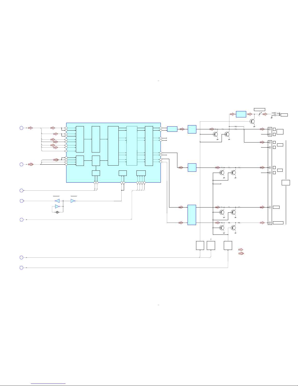
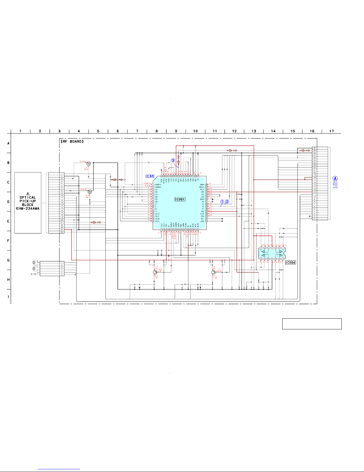
5-7. SCHEMATIC DIAGRAM – RF Board – • See page 42 for Waveforms. • See page 45 for IC Block Diagram.
R020
R006
R007
C040
JL051
R083
R082
R084
R087
R086R085
R066C094C064C095
C060
R065
R029
R046 R036
R044
R025
R024
R023
C055
C052
C051
C048
JL003
R035
C047
JL002
JL001
C050
C003
C028
C090
C002C038
C037C029
L001
R019 R094
R021
C046
R022
C045
C041
C036
C039
C032
C031
JL081
R017
C025C027
C030
C001C023R015
C022
R093
C016
C008
C026
C021C017
C018
C020
C006
R004
CN002
IC001
R001
Q004
R005
Q005
R092
C015D001R097
Q001 Q003
R090
D002C014C007 R003
M3
S1
M2
CN003
CN005
C012
C011
C010
C009
C013
R008
C004
R002
C044
C043
C042
JL006
IC004
470
220
820
0.01
10k
10k
10k
10k
10k10k
10k22
10V
0.10.1
0.1
10k
47k
100 10k
8.2k
0
0
0
47
6.3V
0.1
0.1
0.047
0
0.1
22
10V
0.1
47
6.3V1
2200p100
6.3V
1000p10
47µH
33 33
10M
0.47
12k
1000p
0.01
0.1
0.1
0.1
0.1
470
0.10.1
22
10V
2200p100
6.3V
33
1000p
33
180p
2200p
0.01
22p22p
22p
22p
0.1
47k
6P
CXD1881AR-1
0
2SK3018
47k
2SK3018
0
101SS352-TPH333k
2SB1121-ST-TD 2SB1121-ST-TD
0
1SS352-TPH31010 33k
25P
30P
5600p
2200p
2200p
2200p
5600p
2.2k
0.1
100
330p
0.033
0.033
NJM3403AV(TE2)
RFPCD_LD
SP+
SP-
LIM_SW
SD-
SD+
SP-
SP+
LIM_SW
SD+
SD-
TD-
TD+
A
B
C
D
VMOD
FD-
FD+
FD-
FD+
TD-
TD+
C
D
_
E
L
D
O
N
M
IR
R
D3V
D3V
S
D
E
N
D
A
T
A
_
R
F
C
L
K
_
R
F
F
E
/P
I
F
E
E
F
PI
MIRR
FE/PI
TE
PI
SDEN
DATA_RF
CLK_RF
LDON
FE
T
E
D
V
D
_
L
D
V
M
O
D
C
D
_
L
D
B
RFP
C
D
A
DVD_CD_PD
DVD_LD
CDPDSW
DVDPDSW
DVD_CD_PD
DVDPDSW
CDPDSW
H
G
CD_F
E
H
F
G
CD_F
CD_E
TRK+
TRK-
FCS-
FCS+
MIRR
PI
TE
FE
SDEN
RFAC
D3V
D3V
CLK_RF
DATA_RF
A5V
A5V
AGND
AGND
LIM_SW
A3V
LIM_SW
SP+
SP-
SP+
SP-
LDON
TD-
TD+
FD-
FD+
SD-
SD+
SD+
SD-
CD_LD
CD_LDGND
A
D
E
C
GND
H
VC
RF
F
G
VCC
B
AVC
AVC
FE/PI
DVDPDSW
VMOD
CDPDSW
NC
CD_VR
DVD_CD_PD
LD_GND
DVD_LD
DVD_LDGND
DVD_VR
SUMMING AMP,
PI ERROR AMP,
AVC BUFFER
SACD/CD RF AMP
FOCUS/TRACKING ERROR AMP
PHOTO DIODE
CONTROL SWITCH
(FOR CD)
S
S
PHOTO DIODE
CONTROL SWITCH
(FOR SACD)
(FOR SACD)
AUTOMATIC
POWER CONTROL
AUTOMATIC
POWER CONTROL
(FOR CD)
(LIMIT)
(SLED)
(SPINDLE)
VCC
VEE
The components identified by mark 0 or dotted
line with mark 0 are critical for safety.
Replace only with part number specified.
(Page 30)
 Loading...