

Sony SCD-XB770 Service manual
SCD-XB770
SERVICE MANUAL
Ver 1.0 2001.04
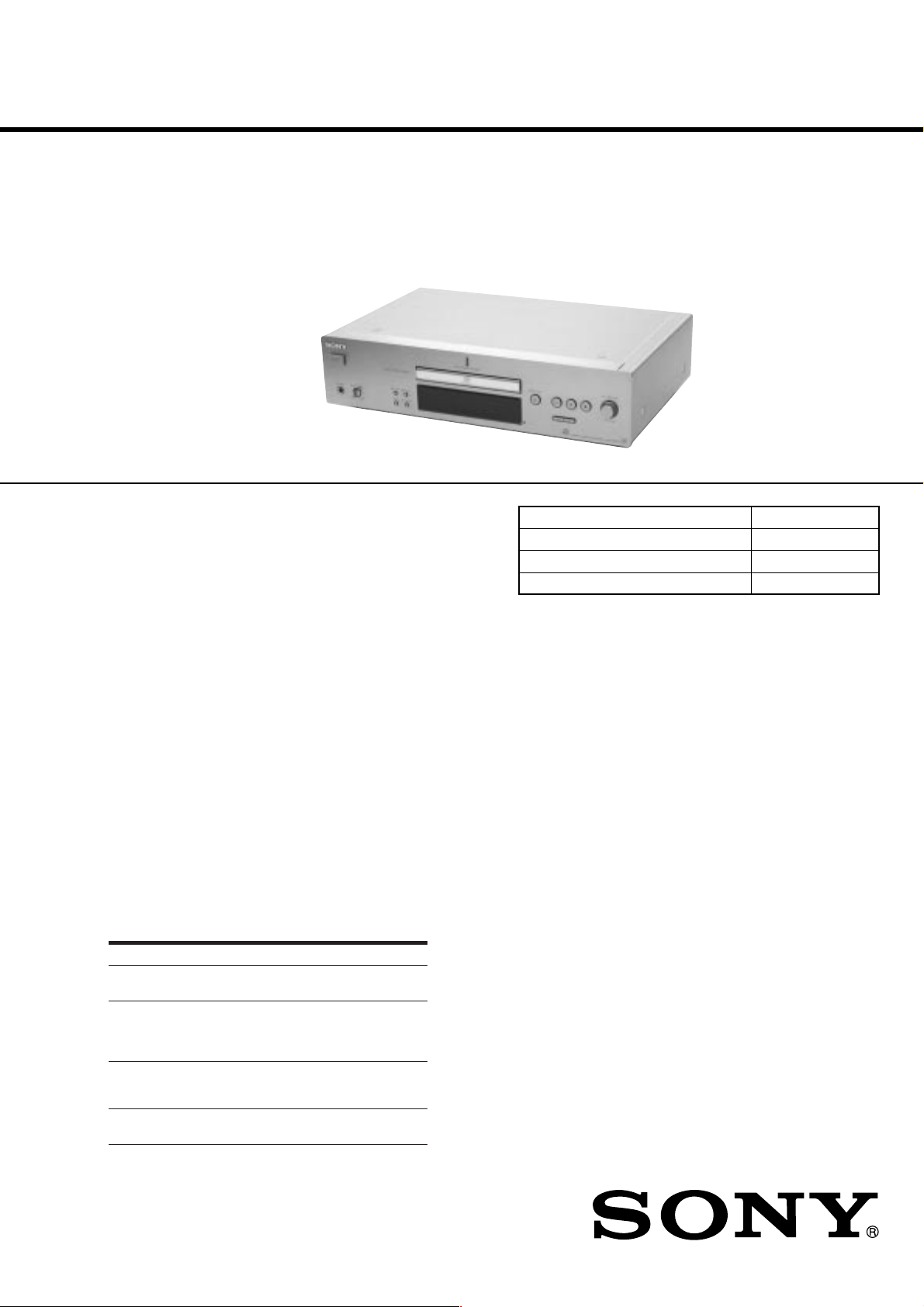
Photo: Silver type
SPECIFICATIONS
AEP Model
UK Model
Model Name Using Similar Mechanism NEW
CD Mechanism Type CDM66B-DVBU6
Base Unit Name DVBU-6
Optical Pick-up Name KHM-230AAA
When a super audio CD is played
Playing frequency range 2 Hz to 100 kHz
Frequency response 2 Hz to 50 kHz (–3 dB)
Dynamic range 104 dB or more
Total harmonic distortion rate
Wow and flutter Value of measurable limit (±0.001 %
When a CD is played
Frequency response 2 Hz to 20 kHz
Dynamic range 99 dB or more
Total harmonic distortion rate
Wow and flutter Value of measurable limit (±0.001 %
Output connector
ANALOG OUT
DIGITAL (CD)
OUT
OPTICAL*
DIGITAL (CD)
OUT
COAXIAL*
PHONES
*Output only the audio signals of the CD
Jack type
Phono
jacks
Square
optical
output
connector
Coaxial
output
connector
Stereo
phone jack
0.0018 % or less
W. PEAK) or less
0.002 % or less
W. PEAK) or less
Output level
2 Vrms
(at 50 kilohms)
–18 dBm
0.5 Vp-p
10 mW
Load impedance
Over 10 kilohms
Light emitting
wave length:
( )
660 nm
75 ohms
32 ohms
General
Laser radiant power: 5.47 uW at 650 nm
*These output is the value measured at a distance of about
200mm from the objective lens surface on the optical pick-up.
Power requirements 230 V AC, 50/60 Hz
Power consumption 25 W
Dimensions (w/h/d) 430 × 111 × 283 mm incl. projecting
parts
Mass (approx.) 5.8 kg
Supplied accessories
• Audio connecting cord
phono jack × 2 (Red and White) y phono jack × 2 (Red
and White) (2)
phono jack × 1 (Black) y phono jack × 1 (Black) (2)
• Remote commander RM-SX700 (1)
• R06 (size-AA) batteries (2)
Design and specifications are subject to change without notice.
SUPER AUDIO CD PLAYER
9-873-846-11 Sony Corporation
2000D0500-1 Home Audio Company
C 2001.4 Shinagawa Tec Service Manual Production Group
SCD-XB770
TABLE OF CONTENTS
1. SERVICING NOTES ............................................... 3
2. GENERAL ................................................................... 5
3. DISASSEMBLY
3-1. Disassembly Flow ........................................................... 8
3-2. Cover ............................................................................... 9
3-3. Front Panel Section ......................................................... 9
3-4. AUDIO Board, MAIN Board.......................................... 10
3-5. Mechanism Deck (CDM66B-DVBU6) .......................... 10
3-6. Base Unit (DVBU-6)....................................................... 11
4. DIAGRAMS
4-1. Notes for Printed Wiring Boards and
Schematic Diagrams ....................................................... 13
4-2. Schematic Diagram – RF Board –................................. 14
4-3. Printed W iring Boards
– RF/LOADING Boards – .............................................. 15
4-4. Printed W iring Board
– MAIN Board (Component Side) – .............................. 16
4-5. Printed W iring Board
– MAIN Board (Conductor Side) – ................................ 17
4-6. Schematic Diagram
– MAIN (1/5)/ LOADING Boards – ............................. 18
4-7. Schematic Diagram – MAIN Board (2/5) – .................. 19
4-8. Schematic Diagram – MAIN Board (3/5) – .................. 20
4-9. Schematic Diagram – MAIN Board (4/5) – .................. 21
4-10. Schematic Diagram – MAIN Board (5/5) – .................. 22
4-11. Schematic Diagram – AUDIO/HP Boards – ................. 23
4-12. Printed Wiring Board
– AUDIO Board (Component Side) – ............................ 24
4-13. Printed Wiring Boards
– AUDIO (Conductor Side)/HP Boards – ..................... 25
4-14. Printed Wiring Boards – DISPLAY/KEY Boards –...... 26
4-15. Schematic Diagram – DISPLAY/KEY Boards –.......... 27
4-16. Printed Wiring Boards
– POWER/TRANS Boards – .......................................... 28
4-17. Schematic Diagram – POWER/TRANS Boards –........ 29
4-18. IC Pin Function Description ........................................... 37
Notes on chip component replacement
• Never reuse a disconnected chip component.
• Notice that the minus side of a tantalum capacitor may be damaged by heat.
Flexible Circuit Board Repairing
• Keep the temperature of the soldering iron around 270 ˚C during repairing.
• Do not touch the soldering iron on the same conductor of the
circuit board (within 3 times).
• Be careful not to apply force on the conductor when soldering
or unsoldering.
CAUTION
Use of controls or adjustments or performance of procedures
other than those specified herein may result in hazardous radiation exposure.
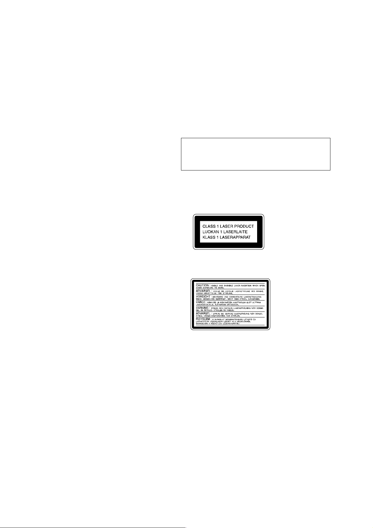
This appliance is classified as a CLASS 1
LASER product.
The CLASS 1 LASER PRODUCT
MARKING is located on the rear exterior.
The following caution label is located
inside the unit.
5. EXPLODED VIEWS
5-1. Cover Section .................................................................. 52
5-2. Front Panel Section ......................................................... 53
5-3. Chassis Section ............................................................... 54
5-4. Mechanism Deck Section (CDM66B-DVBU6) ............. 55
5-5. Base Unit Section (DVBU-6) ......................................... 56
6. ELECTRICAL PARTS LIST ............................... 57
2
SAFETY-RELATED COMPONENT WARNING!!
COMPONENTS IDENTIFIED BY MARK 0 OR DOTTED
LINE WITH MARK 0 ON THE SCHEMATIC DIAGRAMS
AND IN THE PARTS LIST ARE CRITICAL TO SAFE
OPERATION. REPLACE THESE COMPONENTS WITH
SONY PARTS WHOSE PART NUMBERS APPEAR AS
SHOWN IN THIS MANUAL OR IN SUPPLEMENTS PUBLISHED BY SONY.
SECTION 1
SERVICING NOTES
NOTES ON HANDLING THE OPTICAL PICK-UP
BLOCK OR BASE UNIT
The laser diode in the optical pick-up block may suffer electrostatic break-down because of the potential difference generated
by the charged electrostatic load, etc. on clothing and the human
body.
During repair, pay attention to electrostatic break-down and also
use the procedure in the printed matter which is included in the
repair parts.
The flexible board is easily damaged and should be handled with
care.
NOTES ON LASER DIODE EMISSION CHECK
The laser beam on this model is concentrated so as to be focused
on the disc reflective surface by the objective lens in the optical
pick-up block. Therefore, when checking the laser diode emission, observe from more than 30 cm away from the objecti ve lens.
CLEANING OF OPTICAL PICK-UP LENS
In cleaning the lens of optical pick-up, use the air blower.
Never use a cotton swab for cleaning the lens of optical pick-up,
which otherwise causes a trouble.
SCD-XB770
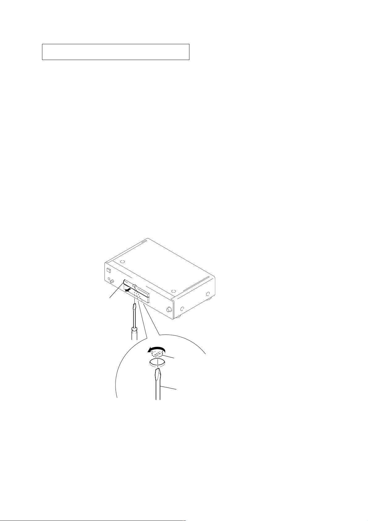
HOW TO OPEN THE TRAY WHEN POWER SWITCH TURNS OFF
tray
A
cam (66)
tapering driver
1
Insert a tapering driver (3 mm in diameter)
in the hole at the bottom of the unit,
turn the cam (66) fully in the direction of arrow A.
3
SCD-XB770
DISPLAY BOARD SERVICE POSITION
In checking the DISPLAY board, prepare jig (extension cable J-8000-024-A : 1.00 mm Pitch, 12 cores, Length 300 mm.)
MAIN board
CN706
DISPLAY board
CN801
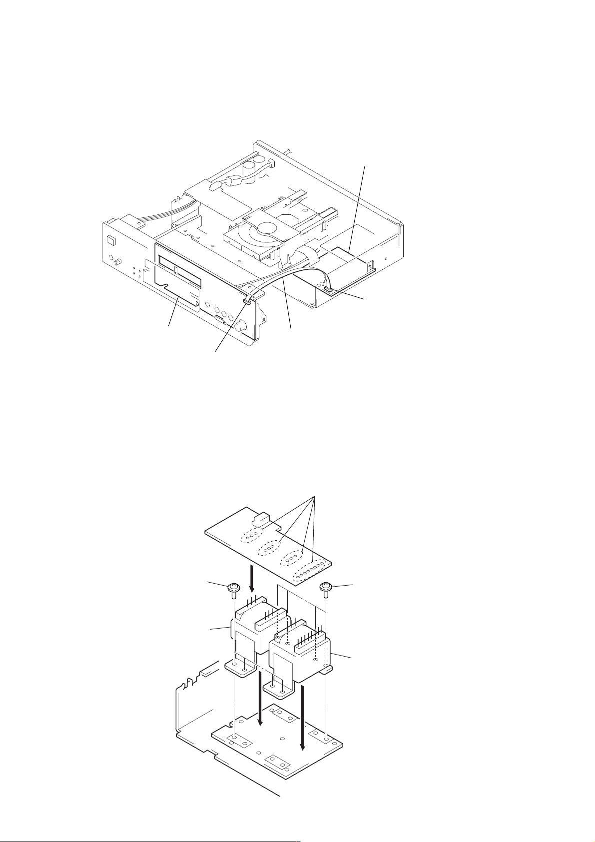
Note: Follow the assembly procedure in the numerical order given.
INSTALLATION OF THE TRANS BOARD
Note : Solder the TRANS board after installing power transformers (T901, T902)
to the chassis.
(To prevent the TRANS board from being cracked.)
3
four screws
(PTTWH3
×
6)
4
Connect jig (extension cable J-8000-024-A)
to the DISPLAY board (CN801) and
MAIN board (CN706).
5
Solder seventeen portions.
four screws
3
(PTTWH3
×
6)
2
power transformer
(T902)
1
power transformer
(T901)
4
SECTION 2
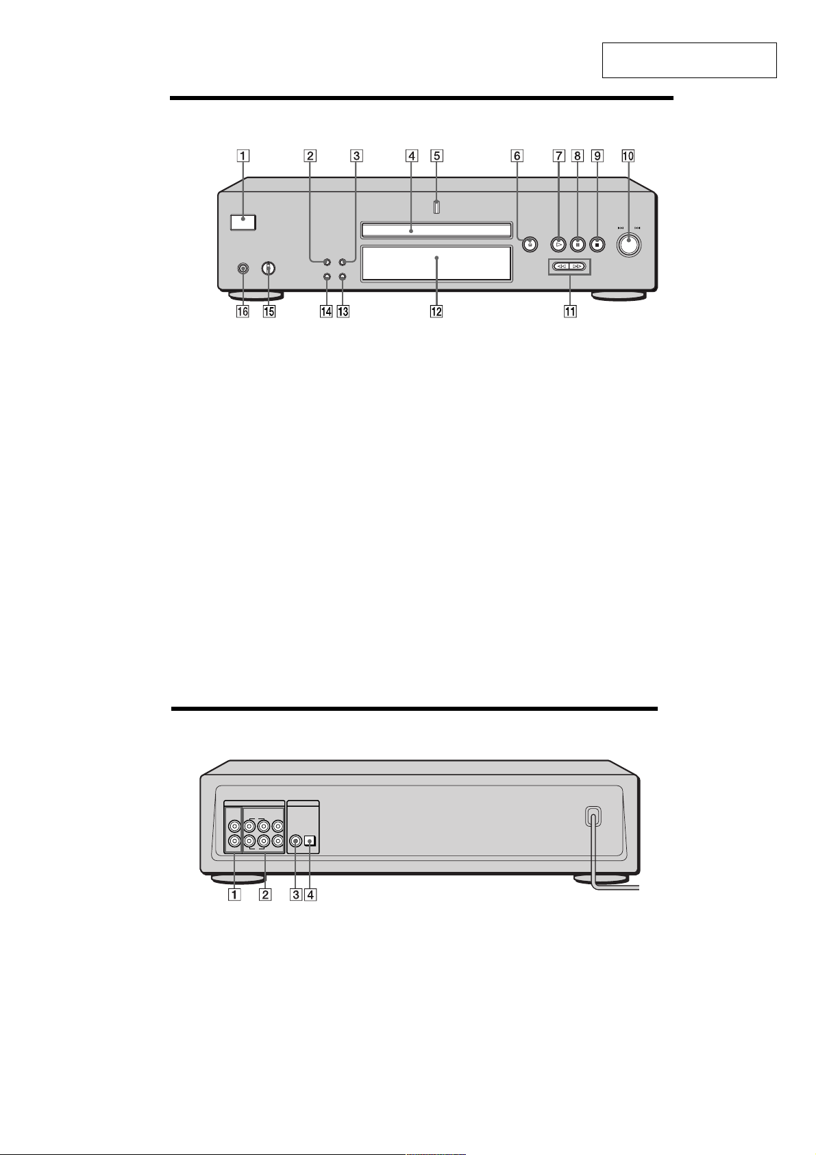
Front Panel Parts Descriptions
GENERAL
SCD-XB770
This section is extracted from
instruction manual.
POWER
PHONES
PHONE LEVEL
MIN MAX
TIME/TEXT SACD/CD
MENU MULTI/2CH
1 POWER switch (14)
Press to turn on the player.
2 TIME/TEXT button (15)
Each time you press the button, the playing time of the
track, the total remaining time on the disc, or TEXT
information appears in the display.
3 SACD/CD button (12)
Each time you press the button, ”SACD“ or ”CD“
appears in the display. Select the type of CD you want
to play.
4 Disc tray (14)
Press A OPEN/CLOSE to open/close the disc tray.
Multi-channel indicator
5
Turns on when you turn on the player, or when the
Multi-channel Super Audio CD is loaded and select
the Multi-channel playback area by pressing MULTI/
2CH.
6 A OPEN/CLOSE button (14)
Press to open the disc tray
.
7 H button (14)
Press to start play.
8 X button (14)
Press to pause play.
9 x button (14)
Press to stop play.
OPEN CLOSE
AMS
PUSH ENTER
0 l AMS L dial (AMS: Automatic Music Sensor)
(13)
When you turn the l AMS L dial
counterclockwise by one click, you go back to the
preceding track; when you turn the l AMS L
dial clockwise by one click, you go to the succeeding
track.
qa m/M buttons (18)
Press to locate a portion you want to play within a
track.
qs Display window (15)
Shows various information.
qd MULTI/2CH button (12)
Press to select the playback area when the 2 channel +
Multi-channel Super Audio CD (page 13) is loaded.
qf MENU (13)
Press to enter the menu.
qg PHONES LEVEL
Adjust the headphones volume.
qh PHONES
Connect the headphones.
During playback of a Multi-channel Super Audio CD,
the same signal that is output from the ANALOG
5.1CH FRONT L/R jacks is output from the PHONES
jack.
Rear Panel Parts Descriptions
ANALOG
2CH OUT 5.1CH OUT OUT
FRONT COAXIAL OPTICALSURR CENTER
L
R
1 ANALOG 2CH OUT L/R jacks (6)
Connect to an audio component (stereo/2 channel)
using the audio connecting cord.
2 ANALOG 5.1CH OUT jacks (5)
Connect to an amplifier equipped with the 5.1CH
input jacks (Multi-channel amplifier, AV amplifier,
etc.) using the audio connecting cords.
3 DIGITAL (CD) OUT COAXIAL connector (7)
Connect to an audio component using the coaxial
digital cable.
4 DIGITAL (CD) OUT OPTICAL connector (7)
Connect to an audio component using an optical
digital cable.
DIGITAL(CD)
L
SUB
R
WOOFER
Note
Only the audio signals of the CD can be output from the
DIGITAL (CD) OUT connectors shown in 3 and 4. Those of the
Super Audio CD cannot be output through DIGITAL (CD) OUT.
5
SCD-XB770
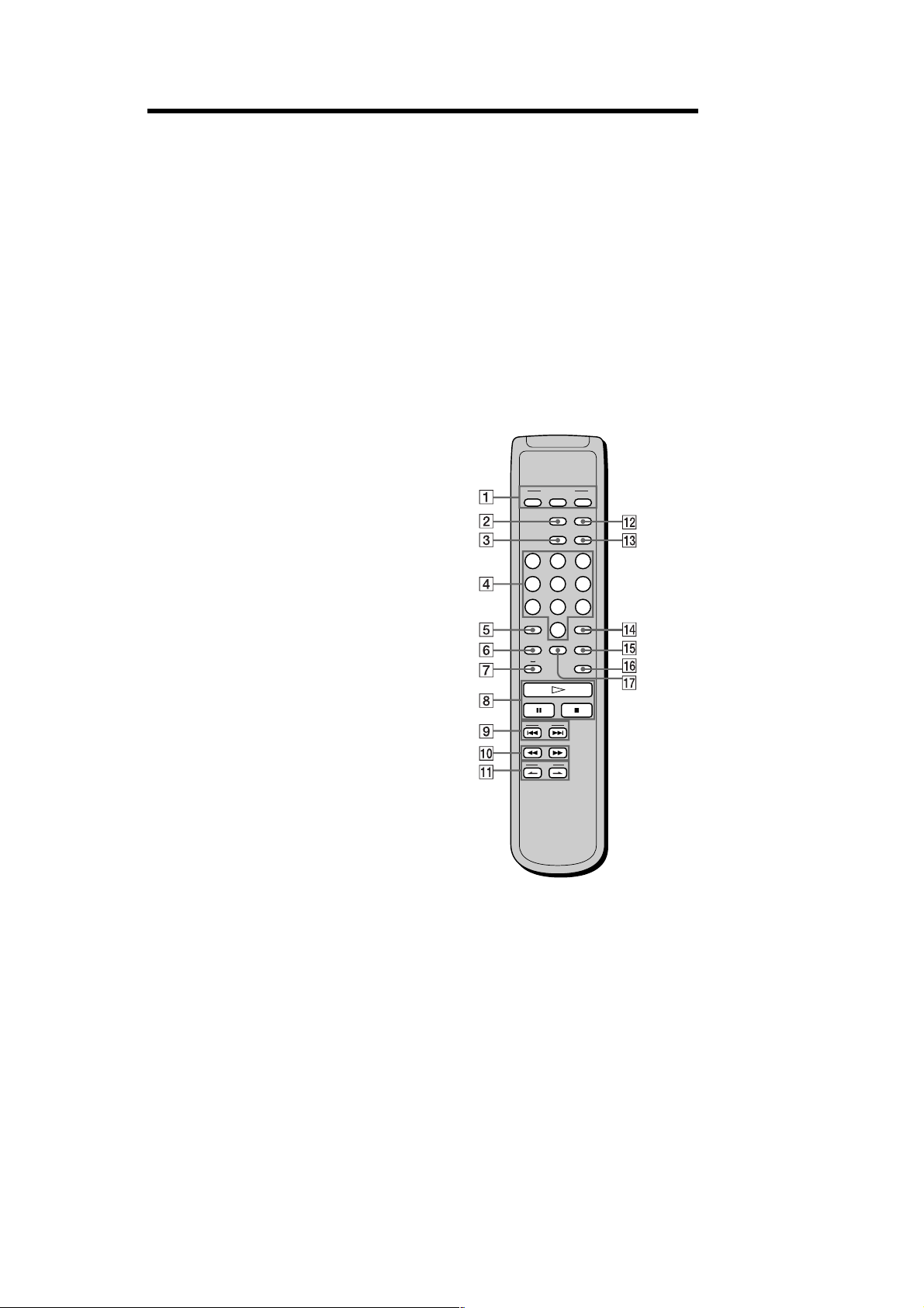
Remote Parts Descriptions
1 CONTINUE button (20)
Press to resume normal play from Shuffle Play or
Programme Play.
SHUFFLE button (20)
Press to select Shuffle Play.
PROGRAM button (21)
Press to select Programme Play.
2 DISPLAY MODE button (16)
Press to turn off the information.
3 TIME/TEXT button (15)
Each time you press the button, the playing time of the
track, the total remaining time on the disc, or TEXT
information appears in the display.
4 Number buttons (18)
Press to enter the track numbers.
5
i
10 button (18)
Press to locate a track numbered over 10.
6 REPEAT button (19)
Press repeatedly to play all tracks or only one track on
the disc.
7 AyB button (20)
Press to select Repeat A-B Play.
8 H button (14)
Press to start play.
X button (14)
Press to pause play .
x button (14)
Press to stop play.
9 AMS ./> (AMS: Automatic Music Sensor)
buttons (18)
Press to locate a specific track.
0 m/M buttons (18)
Press to locate a portion you want to play within a
track.
qa INDEX >/. buttons (18)
Press to locate a specific point marked with an index
signal when you play a disc that has index signals.
qs SACD/CD button (12)
Each time you press the button, ”SACD“ or ”CD“
appears in the display. Select the type of CD you want
to play.
qd MULTI/2CH button (12)
Press to select the playback ar ea when the 2 channel +
Multi-channel Super Audio CD (page 13) is loaded.
qf ENTER button (24)
Press to decide the selection.
qg CLEAR button (21)
Press to delete a programmed track number.
qh LEVEL ADJ button (24)
Press to adjust the output level balance for the Multichannel management function (page 22).
CHECK button (21)
qj
Press to check the programmed order.
PLAY MODE
CONTINUE SHUFFLE
DISPLAY/
MODE
TIME/TEXT
PROGRAM
SACD/CD
MULTI/2CH
123
456
78
>10 ENTER
REPEAT
9
10/0
CLEAR
CHECK
LEVEL
BA
ADJ
AMS
INDEX
11
6
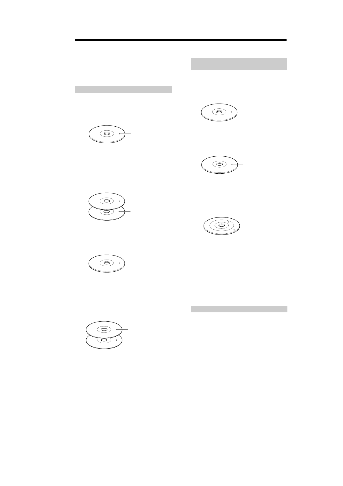
Compatible Disc Types
SCD-XB770
You can play the following discs with this player.
Depending on the type of disc to be played, select the
appropriate indicator by pressing SACD/CD or MULTI/
2CH (pages 14).
Classification by the layer configuration
Super Audio CD (single layer disc)
This disc consists of a single HD (high density) layer.
When you play this disc, the player is set to the Super
Audio CD playback mode automatically.
HD (Super Audio CD)
layer
Super Audio CD (dual layer disc)
This disc consists of dual HD layers and is capable of
extended play over long periods.
When you play this disc, the player is set to the Super
Audio CD playback mode automatically.
Also, as the dual layer disc consists of dual HD layers on
one side only, it is not necessary to turn the disc over.
HD (Super Audio CD)
layer
HD (Super Audio CD)
layer
Conventional CD
This disc is the standard format.
When you play this disc, the player is set to the
Conventional CD playback mode automatically.
CD layer
Super Audio CD + CD (Hybrid disc)
This disc consists of an HD layer and a CD layer. Press
SACD/CD to select the layer you want to listen to. Also,
as the dual layers are on one side, it is not necessary to
turn the disc over.You can play the CD layer using a
conventional CD player.
CD layer
HD (Super Audio CD)
layer
Classification by the channel
configuration of the Super Audio CD
2 channel Super Audio CD
This disc consists of the 2 channel playback area.
When you play this disc, the player is set to the 2 channel
playback mode automatically.
2 channel playback area
Multi-channel Super Audio CD
This disc consists of the multi-channel playback area.
When you play this disc, the player is set to the multichannel playback mode automatically.
Multi-channel playback
area
2 channel + Multi-channel Super Audio CD
This disc consists of the 2 channel playback area and the
multi-channel playback area.
Press MULTI/2CH to select the playback area you want to
listen to.
2 channel playback area
Multi-channel playback
area
You can select the default playback area (2 channel
playback or multi-channel playback area).
1
During stop mode, press MENU.
2
Turn l AMS L until “M/2CH SELECT” appears
in the display .
3
Press l AMS L.
The current playback area appears.
4
Turnl AMS L to select desired playback area,
then press l AMS L.
Incompatible Discs
This player cannot play the following discs. If you try to
play them, the error message “TOC Error” or “NO DISC”
will appear or there will be no sound.
• CD-ROM
• DVD, etc.
7
SCD-XB770
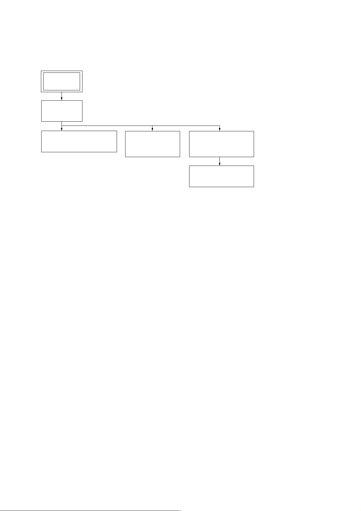
• This set can be disassembled in the order shown below.
3-1. DISASSEMBLY FLOW
SET
3-2. COVER
(Page 9)
SECTION 3
DISASSEMBLY
3-3. FRONT PANEL SECTION
(Page 9)
3-4. AUDIO BOARD,
MAIN BOARD
(Page 10)
3-5. MECHANISM DECK
(CDM66B-DVBU6)
(Page 10)
3-6. BASE UNIT
(DVBU-6)
(Page 11)
8
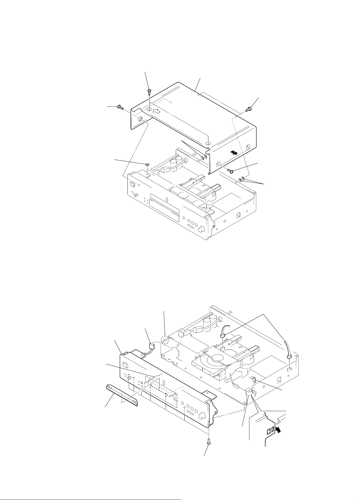
Note: Follow the disassembly procedure in the numerical order given.
)
3-2. COVER
2
two flat head screws (TP)
2
two flat head screws (TP)
4
two washers
(DIA. 3.2)
5
two washers (P)
3
cover
SCD-XB770
1
two screws
2
two flat head screws (TP)
4
two washers (DIA. 3.2
3-3. FRONT PANEL SECTION
4
7
front panel section
1
Pull out the tray.
(Refer to page 3, HOW TO
OPEN THE TRA Y WHEN
POWER SWITCH TURNS
OFF.)
2
loading panel assy
connector
(CN992)
6
two claws
6
two claws
4
two connector
(CN305, 905)
3
wire (flat type)
(12 core)
(CN706)
5
seven screws
(BV/RING)
9
SCD-XB770
)
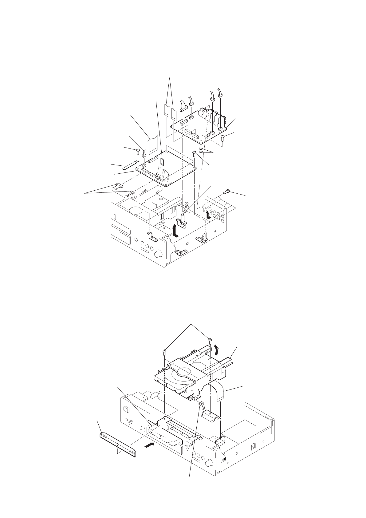
3-4. AUDIO BOARD, MAIN BOARD
8
8
wire (flat type)
(30 core) (CN708)
9
connector
(CN703)
0
screw
(BVTT3
×
6)
qa
wiring stopper
qs
MAIN board
9
two connectors
(CN704, 707)
1
two wires
(flat type) (19 core)
(CN302, 303)
wire (flat type)
(12 core) (CN706)
2
four connectors
(CN301, 304, 305, 306)
5
two washers (DIA. 3.6)
0
three screws
(BVTT3
6
PC board holder
7
AUDIO board
4
screw
(BVTT3
×
6)
3
×
6)
five screws
(BVT/RING)
3-5. MECHANISM DECK (CDM66B-DVBU6)
1
Pull out the tray.
(Refer to page 3, HOW TO OPEN THE TRAY
WHEN POWER SWITCH TURNS OFF.)
2
loading panel assy
3
Push
the tray.
6
three screws
(BVTT3
×
8)
7
mechanism deck (CDM66B-DVBU6)
4
wire (flat type) (30 core
(CN708)
10
5
connector (CN151)
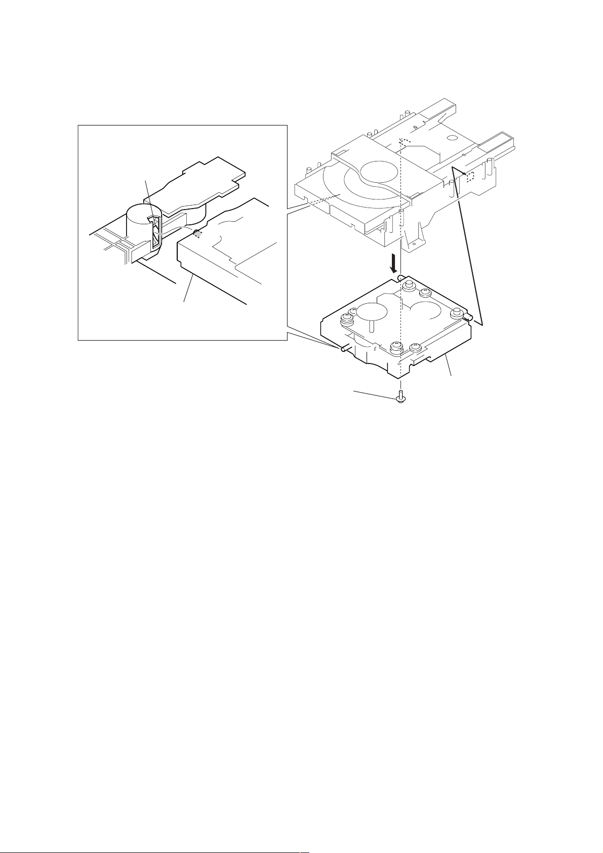
3-6. BASE UNIT (DVBU-6)
– BOTTOM VIEW –
cam (66)
base unit (DVBU-6)
SCD-XB770
2
1
screw (DIA. 12), floating
3
base unit (DVBU-6)
11

SCD-XB770
MEMO
12
SECTION 4
d
DIAGRAMS
SCD-XB770
4-1. NOTE FOR PRINTED WIRING BOARDS AND SCHEMATIC DIAGRAMS
Note on Printed Wiring Board:
• X : parts extracted from the component side.
• Y : parts extracted from the conductor side.
• : Pattern from the side which enables seeing.
(The other layers' patterns are not indicated.)
Caution:
Pattern face side: Parts on the pattern face side seen from
(Conductor Side) the pattern face are indicated.
Parts face side: Parts on the parts face side seen from
(Component Side) the parts face are indicated.
• Main board is multi-layer printed board.
However, the patterns of inter mediate-layer have not been
included in diagram.
• Indication of transistor
C
Q
B
E
These are omitted.
Note on Schematic Diagram:
• All capacitors are in µF unless otherwise noted. pF: µµF
50 WV or less are not indicated except for electrolytics
and tantalums.
• All resistors are in Ω and 1/
specified.
f
•
• 5 : fusible resistor.
• C : panel designation.
Note: The components identified by mark 0 or dotted line
• A : B+ Line.
• B : B– Line.
• Voltages and waveforms are dc with respect to ground
• V oltages are taken with a VOM (Input impedance 10 MΩ).
• Waveforms are taken with a oscilloscope.
• Circled numbers refer to waveforms.
• Signal path.
: internal component.
with mark 0 are critical for safety.
Replace only with part number specified.
under no-signal conditions.
no mark : SACD PLAY
( ) : CD PLAY
Voltage var iations may be noted due to normal production tolerances.
Voltage var iations may be noted due to normal production tolerances.
J : SACD PLAY
c : CD PLAY (ANALOG OUT)
I : CD PLAY (DIGITAL OUT)
: Impossible to measure
∗
4
W or less unless otherwise
• Circuit Boards Location
AC SW board
HP board
KEY board
DISPLAY board
TRANS board
POWER board
LOADING board
RF board
AUDIO boar
MAIN board
1313
SCD-XB770
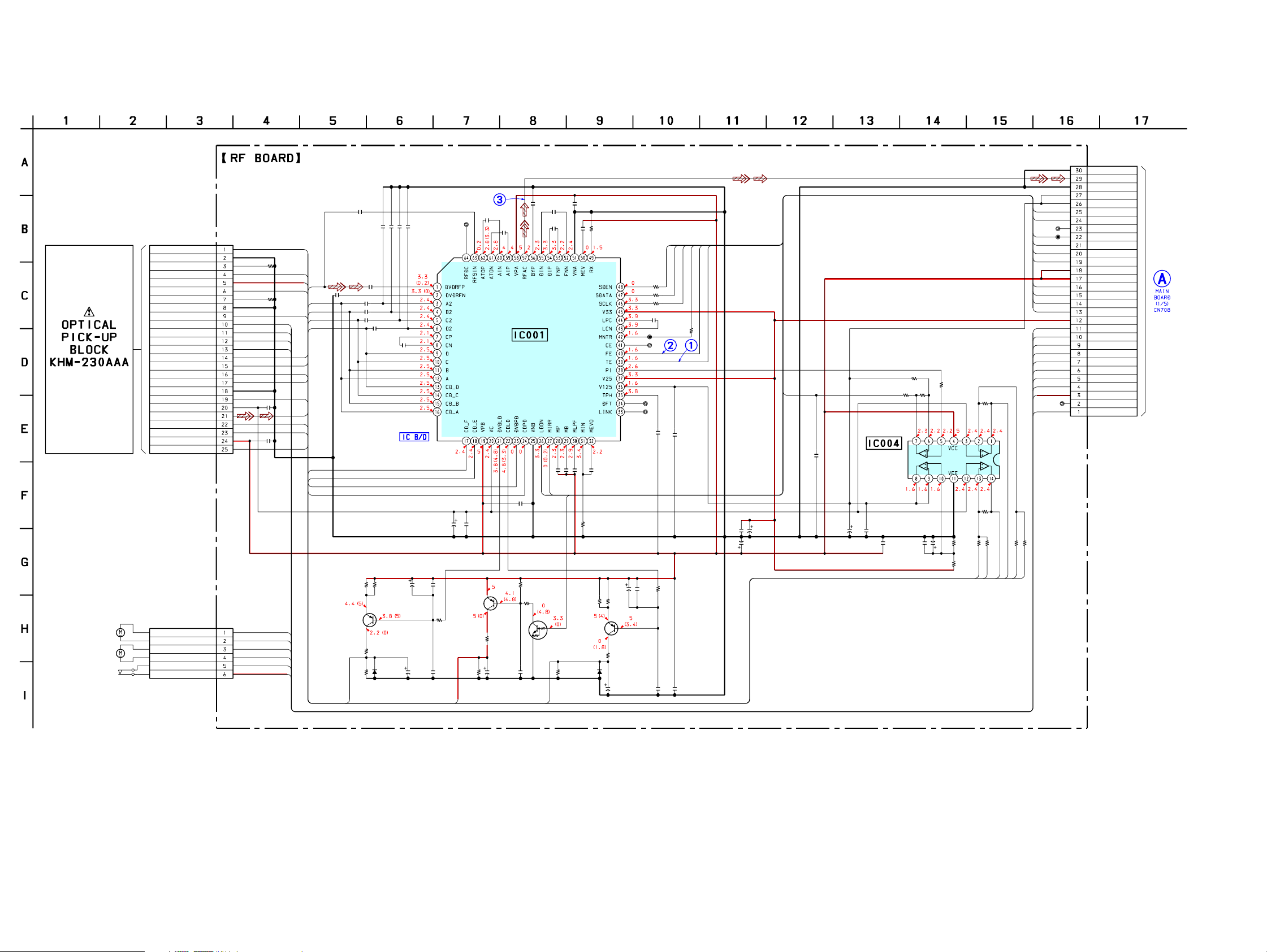
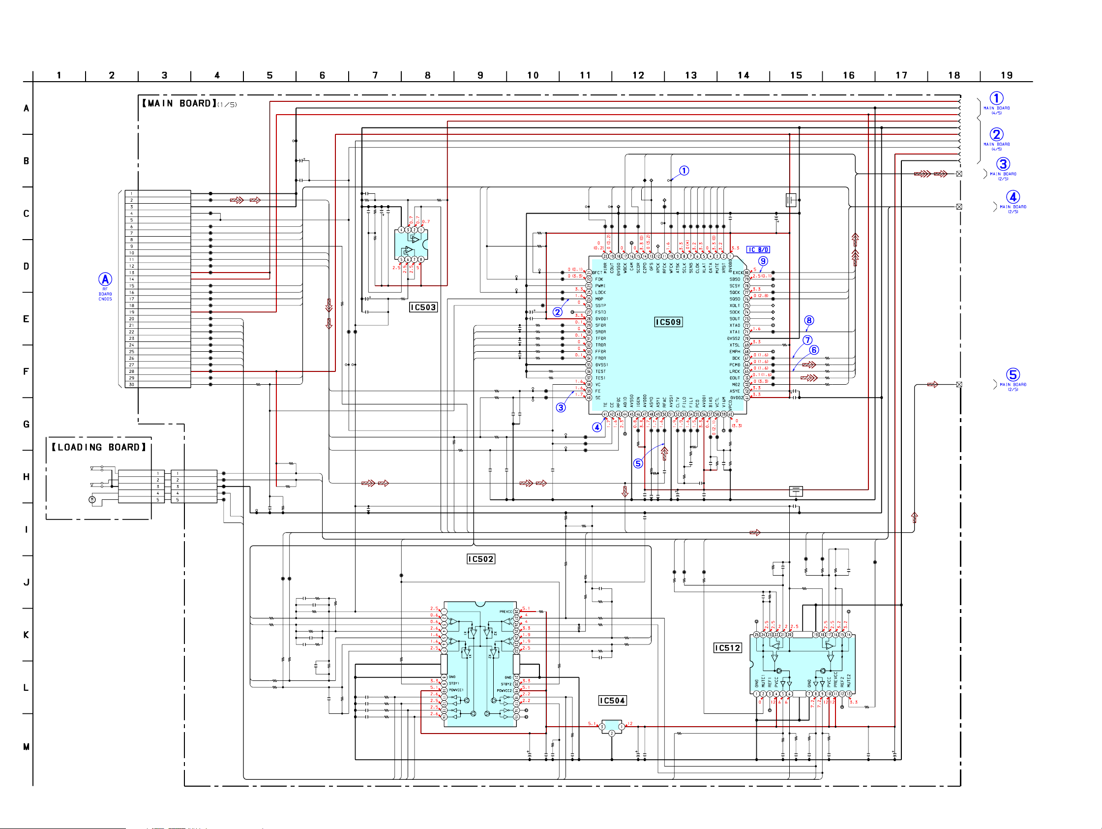
4-2. SCHEMATIC DIAGRAM – RF Board – • See page 30 for Waveforms. • See page 33 for IC Block Diagram.
C041
C032
0.1
SACD/CD RF AMP,
FOCUS/TRACKING
C025
ERROR AMP
IC001
CXD1881R
0.1
R016
R018
C039
0.1
N
O
D
L
1k
1k
0.01
C040
0.01
R
IR
M
DTC144EKA-
B+ SWITCH
D
L
_
D
C
C036
0.1
1000p
C045
330p
C044
C042
C043
0.033
0.033
D
O
M
V
Q005
T146
D002
R003
1SS352
33k
-TPH3
(SPINDLE)
(SLED)
(LIMIT)
C026
0.01
C017 C021
C011
C010
C009
R097
33k
D
L
_
D
V
D
22p 22p
22p
C018
C013
5600p
2200p
2200p
2200p
C008
2200p
C016
180p
3333 2200p
R092
0
D001
1SS352
-TPH3
22p
C020
C023R015R093 C001
100
6.3V
C015
10
C030
22
10V
R017
470
CN003
CN002
25P
6P
CD_LD
CD_LDGND
CD_VR
CD_PD
VMOD
DVD_LD
DVD_VR
DVD_LDGND
DVD_PD
TRK+
TRK-
FCS-
FCS+
A
D
E
C
GND
H
VC
RF
F
G
VCC
B
M3
M2
S1
SP+
SP-
SD+
SD-
LIM_SW
D3V
LIM_SW
CD_LD
R001
0
CD_PD
VMOD
RFP
DVD_LD
R002
100
DVD_PD
TD-
TD+
FD-
FD+
C004
0.1
C006
0.1
SP+
SP-
SD+
SD-
D3V
C012
5600p
A
B
C
D
A
D
E
C
H
RFP
F
G
B
CD_F
CD_E
DVD_PD
CD_PD
Q001
2SB1121-ST-TD
AUTOMATIC
POWER CONTROL
(FOR SACD)
JL081
Q002
2SB1121-ST-TD
B+ SWITCH
D
O
M
V
C031
0.1
C027
0.1
R091
0
C007 C024
R098C022
10 0.01
33k1000p
CN005
30P
MIRR
VMOD
R022
12k
F
E
F
E
N
I
T
F
R
E
R
_
_
/P
A
SD
FE
LK
T
C
A
D
R025
0
0
R024
0
R023
C048
0.047
R035
JL006
JL003
JL002
JL001
C047
0.1
C046
0.1
R021
10M
C038
C002
100
2200p
6.3V
R094R019
3333
Q003
2SB1121-ST-TD
AUTOMATIC
POWER CONTROL
R090
(FOR CD)
0
C037
C029
10
1000p
0
47k
R029
R046 R036
SUMMING AMP,
PI ERROR AMP,
AVC BUFFER
IC004
C095
0.1
100 10k
C060
0.1
PI
C051
0.1
C003
0.1
NJM3403AV(TE2)
C055
C052
47
0.1
6.3
C028
47
6.3
R020
470
C090
1
C050
22
10V
R044
8.2k
C094
22
10V
C064
0.1
R066
R065
10k
R084
10k
R087
10k
10k
R086
10k
R085
10k
10k
E
R082
F
E
_
_
D
F
C
G
CD
JL053
FE/PI
PI
JL052
TE
FE
SDEN
DATA_RF
CLK_RF
LDON
FD-
FD+
TD-
TD+
SD-
SD+
SP-
SP+
D3V
JL051
LIM_SW
10k
R083
H
AGND
RFAC
AGND
AVC
AVC
MIRR
VMOD
DFCT
FE/PI
PI
TE
FE
A5V
A5V
SDEN
DATA_RF
CLK_RF
LDON
A3V
FD-
FD+
TD-
TD+
SD-
SD+
SP-
SP+
D3V
SA/CD
LIM_SW
(Page 18)
1414
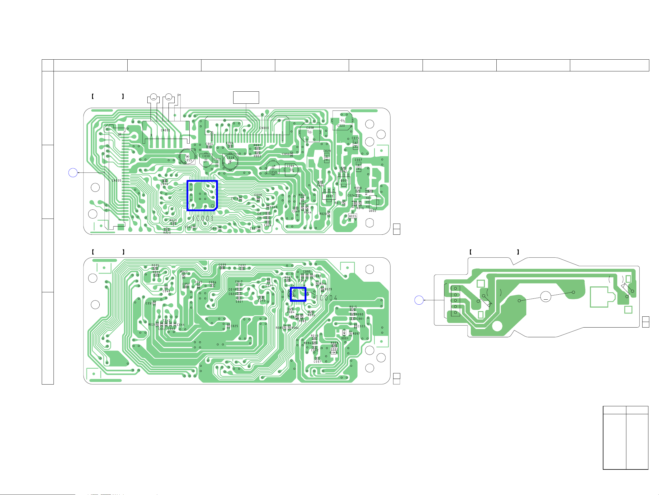
4-3. PRINTED WIRING BOARDS – RF/LOADING Boards – • See page 13 for Circuit Boards Location.
1 2 3 4 5 6 7 8
M3
M
M2
(SLED)S1(LIMIT)
M
OPTICAL PICK-UP
BLOCK
KHM-230AAA
(SPINDLE)
RF BOARD
(COMPONENT SIDE)
A
SCD-XB770
B
C
D
A
MAIN
BOARD
CN708
(Page 16)
RF BOARD
(CONDUCTOR SIDE)
32 17
33
48
49 64
E
16
1
E
E
E
1-680-791-
11
(11)
LOADING BOARD
S152
LOADING
IN
11
1-645-721-
(21)
K
MAIN
BOARD
CN703
(Page 16)
CN151
5
1
S151
LOADING
IN
M
M151
(LOADING)
11
1-680-791-
(11)
• Semiconductor
Location
Ref. No. Location
D001 D-4
D002 D-4
IC001 B-3
IC004 D-4
Q001 B-4
Q002 B-5
Q003 B-4
Q005 B-5
1515
SCD-XB770
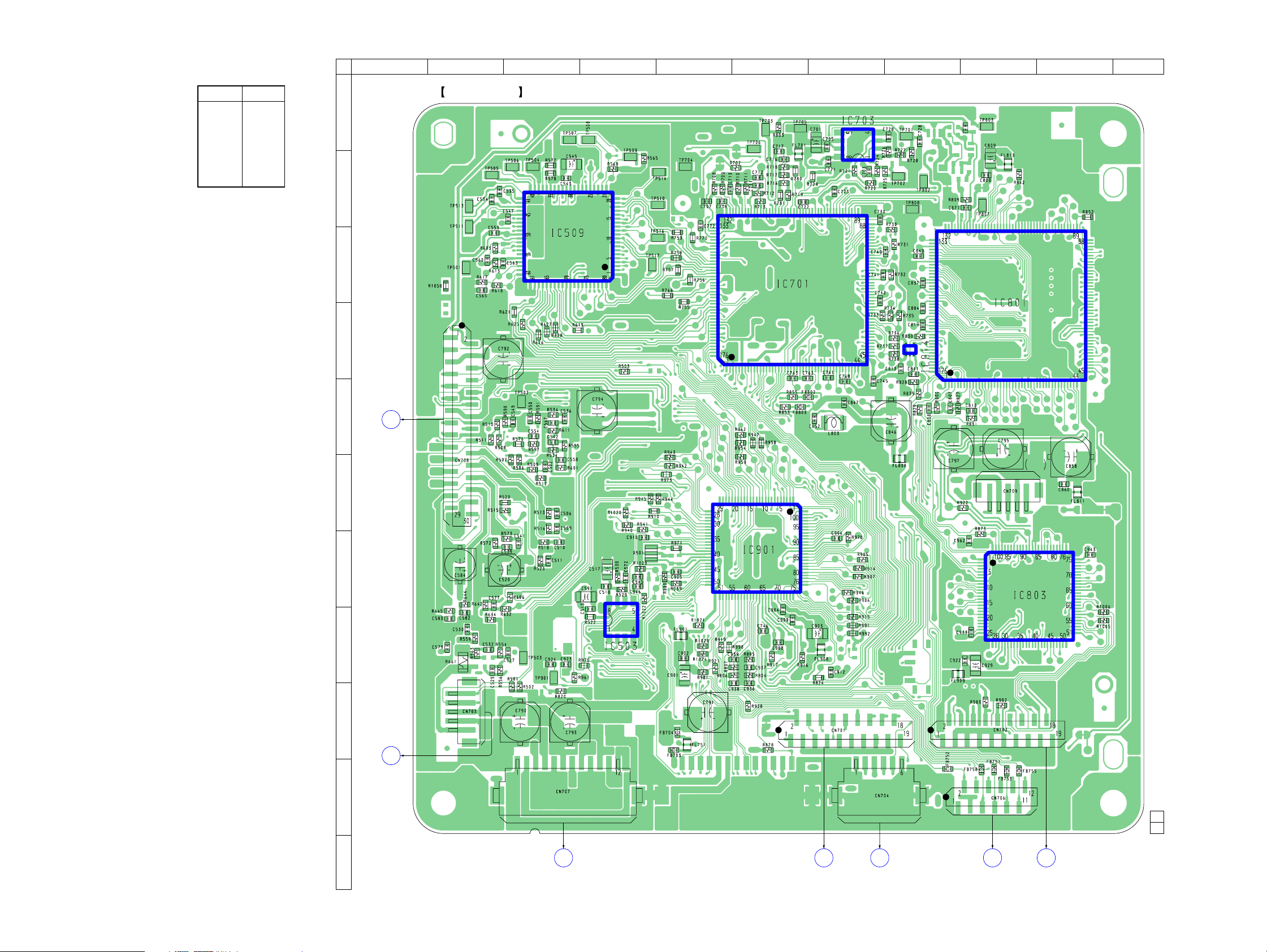
4-4. PRINTED WIRING BOARD – MAIN Board (Component Side) – • See page 13 for Circuit Boards Location.
• Semiconductor
Location
Ref. No. Location
IC503 H-4
IC509 C-3
IC701 C-6
IC703 A-7
IC801 C-9
IC803 G-9
IC814 D-8
IC901 G-6
1 2 3 4 5 6 7 8 9 10 11
MAIN BOARD
A
(COMPONENT SIDE)
C870
B
C
D
54
13
E
F
A
RF
BOARD
CN005
(Page 15)
FOR
RS-232C
15
G
H
1
I
5
K
LOADING
BOARD
CN151
(Page 15)
J
11
1-681-018-
K
E
POWER
BOARD
CN904
(Page 28) (Page 25) (Page 25) (Page 26) (Page 25)
C
AUDIO
BOARD
CN303
B
AUDIO
BOARD
CN304
F
DISPLAY
BOARD
CN801
D
AUDIO
BOARD
CN302
1616
(11)
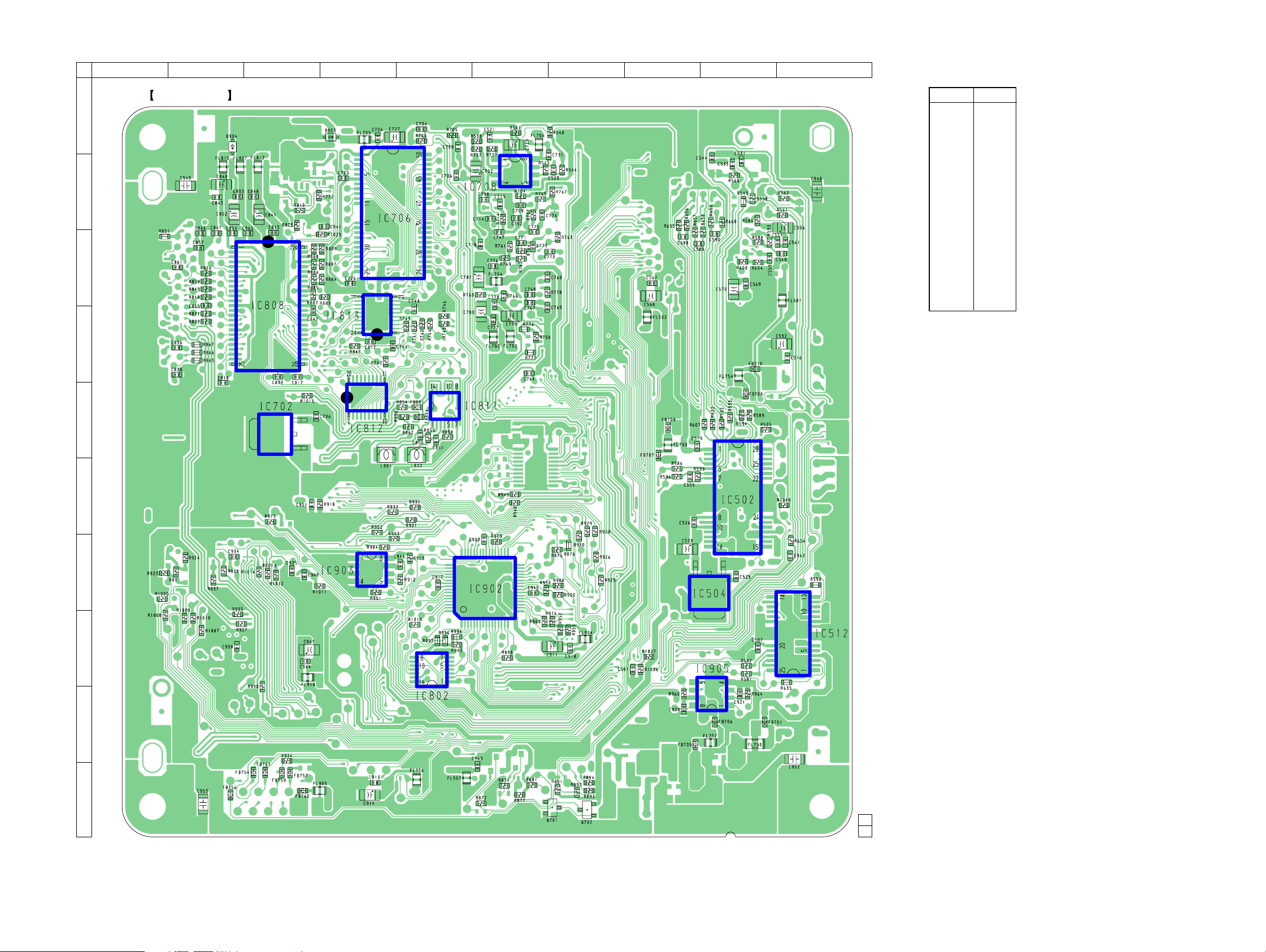
4-5. PRINTED WIRING BOARD – MAIN Board (Conductor Side) – • See page 13 for Circuit Boards Location.
SCD-XB770
1 2 3 4 5 6 7 8 9 10
MAIN BOARD
(CONDUCTOR SIDE)
A
• Semiconductor
Location
Ref. No. Location
D903 A-4
D904 A-2
IC502 F-9
IC504 G-9
IC512 H-10
IC702 E-3
IC706 B-4
B
IC708 B-6
IC802 H-5
IC808 C-3
IC811 E-5
IC812 E-4
IC813 D-4
IC902 G-6
C
IC903 G-4
IC905 I-9
Q701 J-7
Q702 J-7
D
E
2
3
1
F
48 33
49
32
31
G
64
116
17
2
H
I
J
E
E
11
1-681-018-
(11)
1717
SCD-XB770
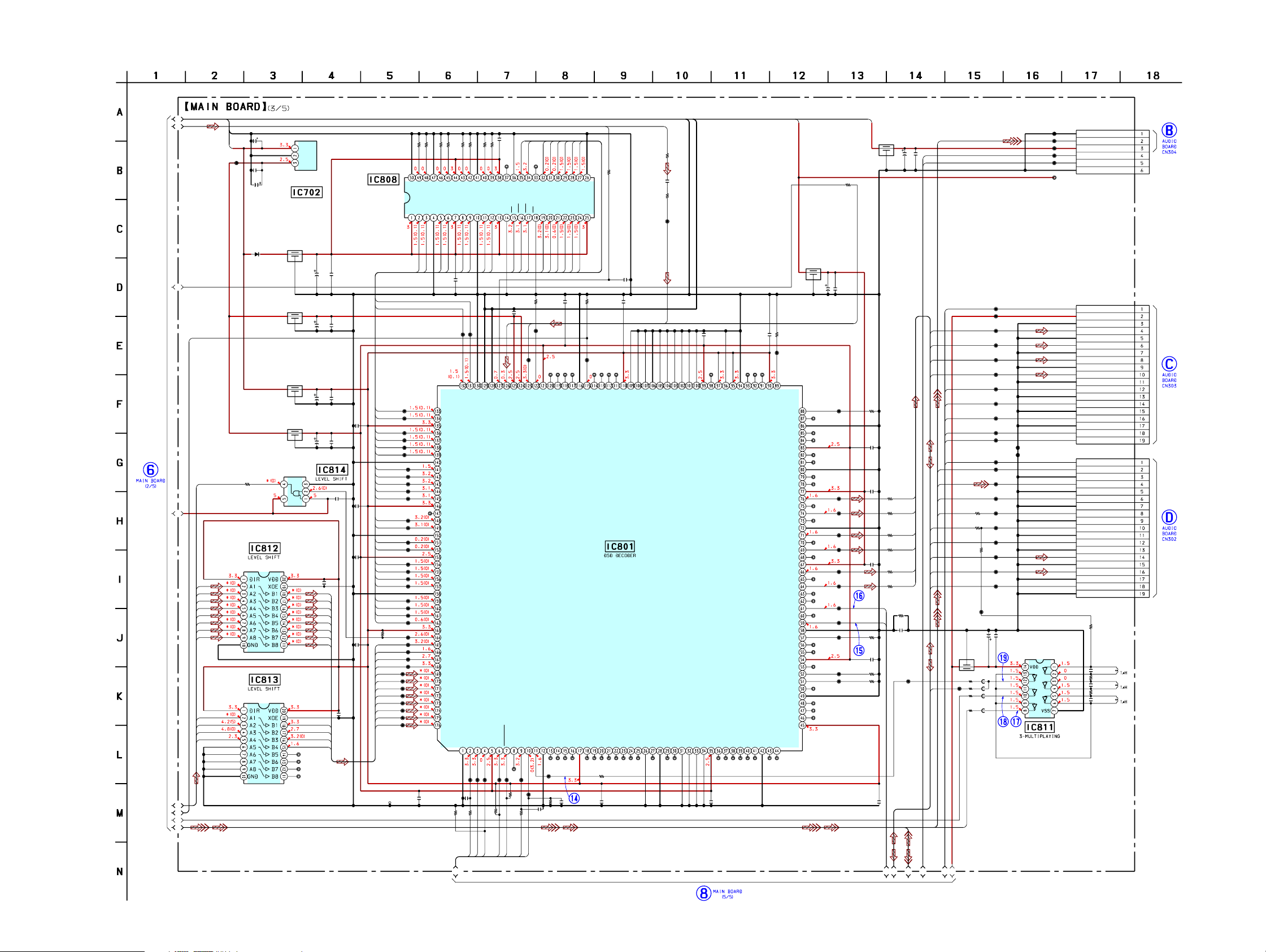
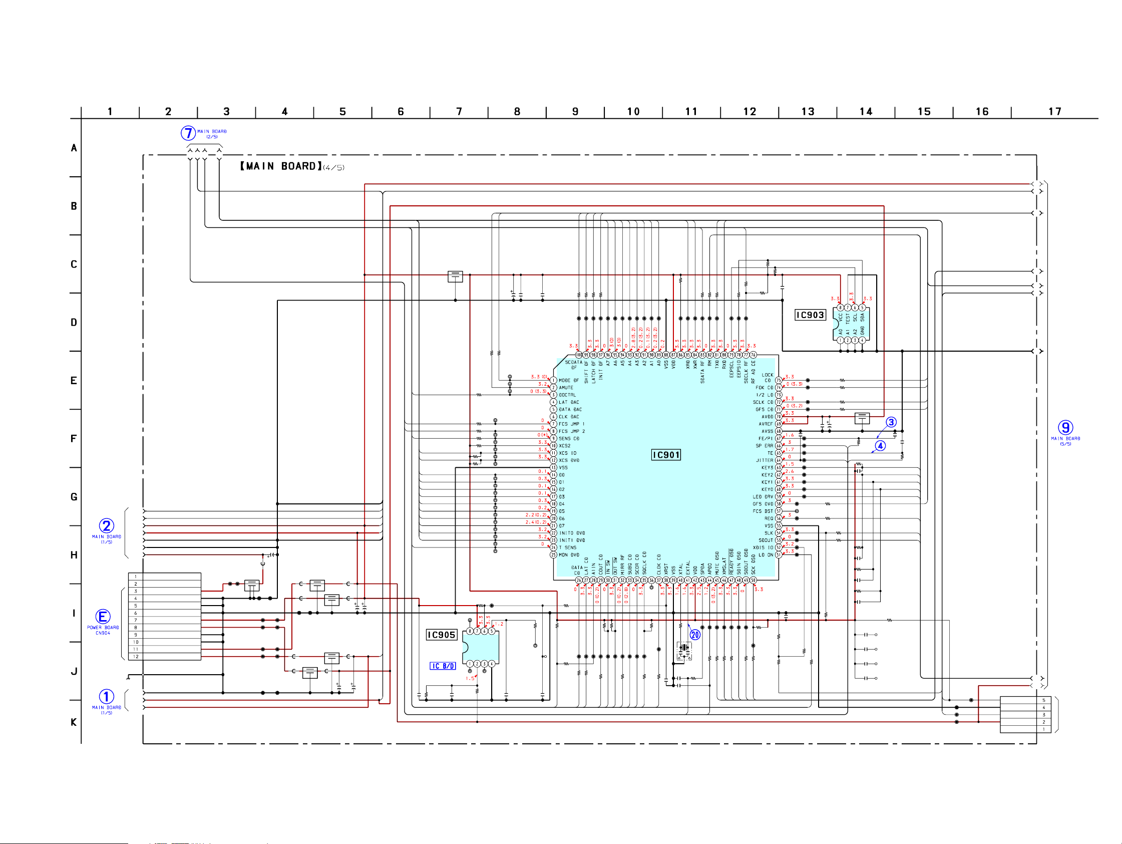
4-6. SCHEMATIC DIAGRAM – MAIN (1/5)/LOADING Boards – • See page 30 for Waveforms. • See page 33 for IC Block Diagram.
TP501
(AGND)
C592
10
10V
C516
DATA_RF
CLK_RF
LDON
SA/CD
LIM_SW
R501
10k
0.1
C
VC
WAVRB BUFFER,
DRVC BUFFER
R1027
68k
2
E
-T
M
3
A
0
4
5
0
4
IC
3
M
J
N
TE
MDP
WAVRB
FOK
LOCK
R565
10k
R568
10k
TP509
(DFCT)
TP508
(FOK)
TP507
(LOCK)
C545
10 10V
C543
SFDR
SRDR
TFDR
TRDR
FFDR
FRDR
R549
0
R561
1k
C534 C535
10000p 2200p
FE
0.1
C588
2200p
C589
2200p
C590
1000p
R560
1k
R558
47k
R562
1k
JL566
JL565
JL564
JL563
JL562
JL560
1k
R655
JL559
1k
R656
JL558
2.2k
R657
JL557
2.2k
R658
JL556
2.2k
R659
JL555
2.2k
R660
0
R578
0
R577
TP506
(FE)
JL554
JL553
TP505
(SE)
C533C531
2200p0.047
C544
0.1
R511 R510
3.3k 1.6k
MIRR
TP510TP514
(COUT)(MIRR)
JL569
JL561
TP513
(TE)
JL568
JL570
JL572
TP511
(PI)
C501
TP503
(DRVC)
1
R1026
10k
C518
1
0.1
k
0
V
2
2
0
7
2
1
5
C
0
0
3
1
5
R
7
1
5
C
GND
k
0
2
2
9
2
5
R
C591
C513
0.1
JL546
C519
1
R522
10
10V
0
RFAC
MIRR
VMOD
DFCT
PI
TE
FE
SDEN
0
3
0
5
R
7
4
5
L
J
)
C
V
(A
4
0
5
P
T
FE
TE
IN_SW
PI
RFAC
R502
10k
OUT_SW
R654C942
1k0.1
S151
(LOADING OUT)
S152
(LOADING IN)
M151
(LOADING)
(Page 14)
OUT_SW
IN_SW
GND
LOAD+
LOAD-
CN708
30P
AGND
RFAC
AGND
AVC
AVC
MIRR
VMOD
DFCT
FE/PI
PI
TE
FE
A5V
SDEN
DATA_RF
CLK_RF
LDON
A3V
FD-
FD+
TD-
TD+
SD-
SD+
SP-
SP+
D3V
SA/CD
LIM_SW
CN151
CN703
5P
5P
OUT_SW
IN_SW
GND
LOAD+
LOAD-
CL1062
CL1063
CL1064
CL1065
CL1066
CL1067
CL1068
CL1069
CL1070
CL1071
CL1072
CL1073
CL1074
CL1075
CL1076
CL1077
CL1078
CL1079
CL1080
CL1081
CL1082
CL1083
CL1084
CL1085
CL1086
CL1087
CL1088
CL1089
CL1090
CL1093
CL1091
LOAD-
FD-
FD+
TD-
TD+
SD-
SD+
SP-
SP+
R1018
22
2
9
0
1
L
C
LOAD+
TP502
(DGND)
A5V
AGND
A3V
(Page 21)
D5V
DGND
D3V
DRVC
AVC
M12V
BCLK
MDAT
LRCK
DOUT
768FS
LOCK
FOK
MIRR
COUT
SCOR
GFS
SCLK
SENS
CLOK
XLAT
DATA
XRST_CD
SQCK
SQSO
MD2
MDP
RF_AC
SPIN
SPDA
TE
FE
FJMP1
FJMP2
SP_ERR
WAVRB
MGND
DSP_BUS
SPC970_BUS
ANALOG_BUS
)
3
2
WFCK
C2PO
0
CL502
(MNT3)
SCOR
8
7
5
L
J
JL576
7
7
5
3
7
JL
5
L
J
R584
33k
C547
0.1
T
5
N
L
C
(M
TP517
(WFCK)
CL505
(MNT0)
GFS
8
9
0
1
L
C
)
6
K
1
C
5
F
P
T
(R
CL504
(MNT1)
DIGITAL SIGNAL PROCESSOR,
DIGITAL SERVO PROCESSOR
IC509
CXD3068Q
3
1
8
8
5
5
JL
JL
k
0
1
8
k
8
0
5
0
R
1
3
9
5
R
C551
0.47
C548
0.01
C502
0.1
7
8
5
L
J
5
9
8
8
5
5
JL
JL
p
0
0
0
0
1
3
5
5
C
XLAT
CLOK
SCLK
SENS
1
3
5
6
9
9
9
9
5
5
5
5
L
L
JL
JL
J
J
4
0
2
9
9
9
5
5
5
k
L
0
JL
JL
J
1
8
k
0
1
6
R
4
0
6
R
C559
0.1
5
0
1
6
0
3
5
k
0
.0
C
6
.3
0
R
3
C556 C561
10 10V 0.1
GSCOR
C2PO
WFCK
DATA
MUTE_CD
XRST_CD
8
0
2
9
0
0
5
6
6
0.1
L
L
L
J
J
J
JL603
1
0
6
9
7
R618
9
9
JL
5
5
470k
L
L
J
J
R617
1M
3
5
3
p
1
M
6
6
0
.1
6
1
5
5
0
0
C
R
C
1
FL502
C568C567
10
10V
JL616
JL615
JL614
JL613
JL612
CL508
CL507
CL506
JL611
JL610
R619
0
JL609
JL608
JL607
JL606
JL605
JL604
C570
10
10V
C569
0.1
FL501
C587
0.1
EXCK
SBSO
SQCK
SQSO
768FS
R628
0
BCLK
R627
0
MDAT
R626
0
LRCK
R625
330
DOUT
MD2
R621
0
EXCK
SBSO
SA/CD
CLK_RF
DATA_RF
SDEN
LDON
LOAD_IN
LOAD_OUT
IN_SW
OUT_SW
MUTE_2D
MUTE_LOAD
SP_ON MUTE_CDA5V
VMOD
LIM_SW
GSCOR
CL501
COUT
(GND)
4
1
7
7
5
5
L
L
J
J
RF_AC
(Page
21)
(Page 19)
(Page 19)
(Page 19)
TFDR
TRDR
FFDR
FRDR
FJMP2
JL519 JL520
R607
4.7k
R602
4.7k
R596 R586
00
R592
4.7k
R595
4.7k
FJMP1
SPIN
C527
R508
SP_ERR
MUTE_2D
JL521
R534C536
3.3k0.47
C562
R611
R601
C558
R524
680p
10k
22k
22k
680p
R555C542
3.3k0.47
R591C550
2.7k680p
C506 R513
R599C555
2.7k680p
0.1 10
C509 R516
0.1 10
C510
0.1
C511
0.1
R520
0
R518
10
R523
10
TD+
TD-
FD+
FD-
FOCUS/TRACKING
COIL DRIVE,
SLED MOTOR DRIVE
IC502
BA5983FP
C528
10
10V
2.2k
R512
0
C549
R509
0.1
R576
0
JL516
JL517
C526
0.1
10k
R590
10k
R505
4.7k
R506
R589
4.7k
10k
C554
0.1
+5V REGULATOR
µPC3905T-E1
IC504
OGI
33k
SFDR
SRDR
R594
33k
C520
22
16V
R507
3.3k
R597
R515
0
R572
10
0
1
3
7
5
R
C541C539
0.10.1
SD-
SD+
LOAD_IN
LOAD_OUT
MUTE_LOAD
JL528
R661
C525
0.1
LOAD- LOAD+
JL543JL542
R635
R582R581
010k10k
JL630
SPINDLE/
LOADING
MOTOR DRIVE
IC512
BA5912AFP-YE2
0
560p
R554
2.7k
R556
2.7k
C529
560p
JL637
R563 R644
10 10
C532
0.1
SPDA
JL617
JL618
R642 C577
R606
R632
10k
R634
6.8k
10
10
9
45
.1
6
55
0
R
R
0
3
5
C
SP+
33k 10000p
6.8k
1
4
6
JL
.1
0
3
C582
58
C
0.1
SP-
SP_ON
JL621
JL636
R598
0
C584
C579
22
16V0.1
1818
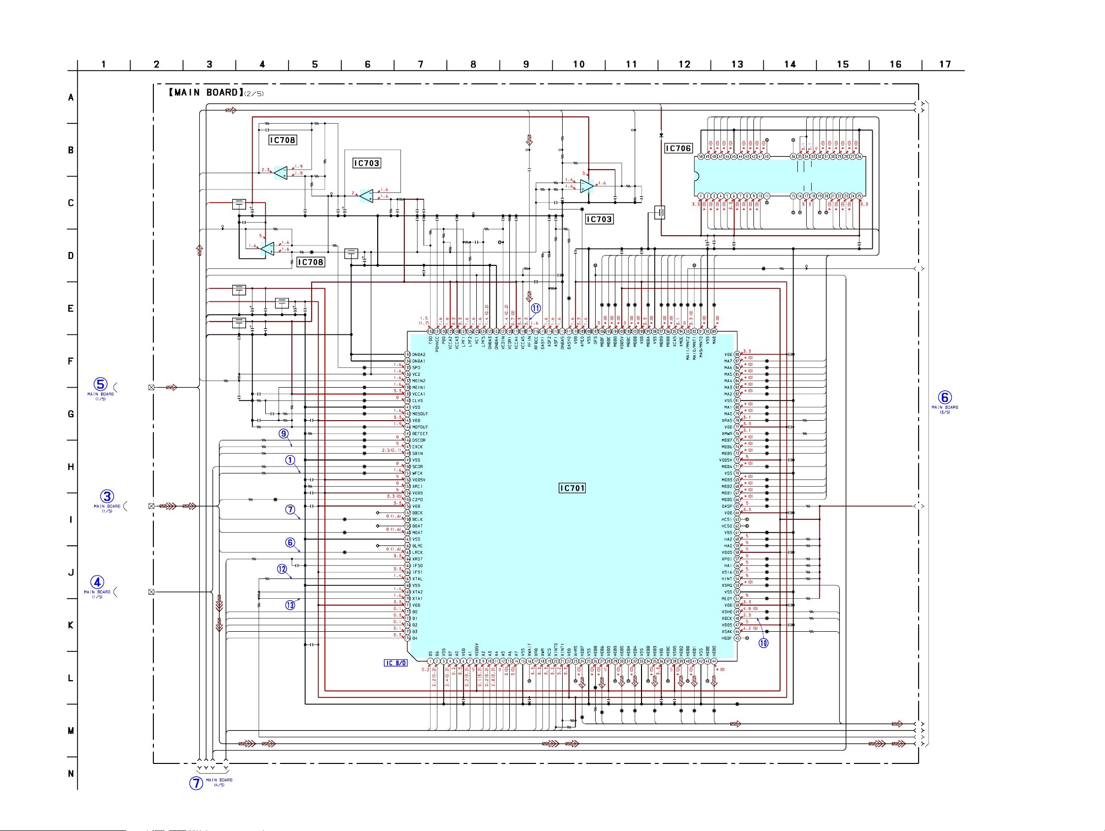
4-7. SCHEMATIC DIAGRAM – MAIN Board (2/5) – • See page 30 for Waveforms. • See page 33 for IC Block Diagram.
100k
R545
1500p
(Page 18)
(Page 18)
(Page 18)
ANALOG_BUS
SPC970_BUS
DSP_BUS
MDP
RF_AC
SPIN
FJMP1
FJMP2
SPDA
FE
TE
SP_ERR
WAVRB
768FS
GSCOR
EXCK
SBSO
WFCK
C2PO
BCLK
MDAT
LRCK
DOUT
DATA_RF
CLK_RF
SDEN
LDON
MIRR
LOCK
FOK
COUT
GFS
MUTE_CD
SENS
SCLK
DATA
XLAT
CLOK
MD2
SQSO
SCOR
SQCK
SA/CD
XRST_CD
SP_ON
VMOD
MUTE_2D
MUTE_LOAD
LOAD_IN
LOAD_OUT
IN_SW
OUT_SW
LIM_SW
C523
SPINDLE MOTOR
DRIVE
IC708(2/2)
C731
NJM3404AM-TE2
C780
10
10V
R761
2.2k
R750
R777
C729
10
10V
0.1
7
4
IC708(1/2)
C777
0.1
C781
10
10V
C772
0.1
R764
1M
C771
0.047
R759
R758
R757
R756
0
R766
0
R768
100
R776 C766
10k
0
NJM3404AM-TE2
1
R701
220k
8
6
5
R704
220k
FL702
C776
0.1
C773 R763 R769
0.47 8.2k 2.2k
R762
0
0
0
CL791R755
(C2PO)0
0 100p
MDIN
MDP
FL706
A5V
TP706
(SPIN)
SPIN
DRVC
AVC
FL703
D5V
D3V
DGND
A3V
FL704
AGND
C775
0.1
R765
22k
MDIN
R767
47k
C774
4700p
GSCOR
EXCK
SBSO
SCOR
WFCK
C2PO
BCLK
MDAT
LRCK
XRST_DVD
D0
D1
D2
D3
D4
R544
100k
(2/2)
R540
2
3
C521
1500p
R703
C779
10
10V
C770
0.1
22k
R770
0
0.1
C769
100k
R778
0.1
C768
10k
R541
100k
R538
100k
CL1008
100k
BUFFER
C778
0.1
C767
0.1
C765
0.1
CENTER VOLTAGE
NJM3404AM-TE2
TP705
(DVC)
C701
10
10V
C705
0.1
R702
100k
FL701
(1/2)
JL786
JL785
CL796
CL795
CL794
CL793
CL792
CL750
JL784
JL783
JL782
JL781
CL781
CL780
CL787
(BCK)
CL786
(MDATA)
CL785
(LRCK)
GENERATOR
IC703(2/2)
1
C702
10
10V
(2/2)
2
3
CL790
CL789
CL788
R705
100k
R706
100k
C704
C798C799
0.10.01
C706
0.1
1
M
1
8
0
7
R
C752
0.1
D5
D6
TP704
C709
(AGND)
0.1
C708C707
1000p33p
R709
68k
R707
100
C764
0.1
A0
D7
C712
R712
220p
10k
C711
R710
0.01
10k
CL703
R711
2.2k
A1
A4
A2
A3
RF_AC
R713
10k
C713
0.1
R714
10k
CL779
C763
0.1
A7
A6
A5
APDO
R729
0
TP702TP703
(APDQ)(RFAC)
R725
C715
3300p
C714
1
XHRD
1.8k
R726
100k
R724
6
C720C703
0.111k1k
R718
10k
7
0
7
L
C
IC701
CXD1882R-1
R745
47k
8
5
7
4
CL701
IC703(1/2)
NJM3404AM-TE2
INTEGRATOR
R780
0
0
1
.1
7
0
L
C
8
1
7
C
6
7
7
L
J
8
7
7
L
C
R744
22
7
7
7
L
SDEF
C
SD7
47k
R746
R721
33k
R720
C716
0.47
1
.0
0
k
7
0
1
0
7
1
C
7
1
R781
7
0
R
0
0
1
1
7
6
4
1
7
7
C
R
k
1
9
1
7
R
SACD DECODER
XINIT1
XINIT0
XCS1882
XHWR
D3V
JIT
TP701
(JIT)
R727
3.3k
R728C721
C728
10k1
0.1
(1/2)
C722
C723
0.1
0.1
BDB
BDC
BDD
BDE
BDF
8
5
6
7
1
1
1
1
7
7
7
7
L
J
JL
JL
JL
JL774 JL773 JL772 JL771 JL769JL770
0.1
C762 C761
5
7
7
CL776
L
C
SD5
SD6
BD9
BDA
9
0
1
1
2
2
7
7
7
L
JL
JL
J
0.1
CL773
4
7
7
L
C
SD4
SD3
D903
1SS367
D-RAM
IC706
GM71VS18163CLT-6
FL705
BD8
XCAS
2
3
2
2
7
7
JL
JL
C760
0.1
SCD-XB770
A1
A2
BDE
BDF
BDC
BDA
BDD
BDB
BD9
BD8
JL1080
.
D
GN
I/O12
I/O13
I/O14
I/O15
3
D
I/O
VD
I/O2
I/O1
I/O0
BD3
BD2
BD1
BD0
C727
10
10V
CL918
(RFD)
MA9
XMOE
4
2
7
JL
SD2
MA8
7
8
1
2
2
1
7
7
7
L
L
L
C
C
C
JL726
2
7
CL771
7
L
C
CL770
SD0
SD1
8
10
.C
N
I/O
I/O9
GND
I/O
I/O11
4
.C.
N
I/O7
I/O6
I/O5
I/O
VDD
5
7
10
L
J
BD6
BD7
BD5
BD4
C725C724
0.10.1
CL1017
JL929
JL731
JL734
JL735
JL736
JL737
JL738
JL740
JL741
JL742
JL743
JL744
JL745
JL746
JL750
JL751
JL752
JL753
JL754
JL755
JL756
JL757
JL758
JL759
JL760
JL761
JL762
JL763
JL764
JL765
JL766
JL767
JL768
JL1088
JL777
XCAS
XMOE
JL1081
.C.
OE
N
CAS
LCAS
U
.C.
N
N.C.
WERAS
7
76
7
0
0
1
WE
JL1
JL
RAS
R772
TP802
22
.1
0
0
3
7
C
MA7
MA6
MA5
MA4
MA3
MA2
MA1
MA0
R730
22
RAS
C740
0.1
R731
22
BD7
BD6
BD5
C741
0.1
BD4
BD3
BD2
BD1
BD0
R732
10k
C742
0.1
R733
10k
R734
10k
C743
0.1
R735
10k
R736
10k
R737
10k
R738
10k
R740
10k
C744 R741
0.1 22
C745
R742
0.12222
R743
MA5
MA6
MA7
MA4
MA8
MA9
D
A4
A5
A7
A6
A8
A9
.C.
N
N.C.
9
78
7
0
10
L1
J
JL
MA0
GFS_V
GN
DD
3
2
1
V
A
A
A0
A
MA3
MA2
MA1
C726
0.1
A3
(Page 20)
WE
A4
XSRQ
XSHD
XDCK
XSAK
A5
A6
A7
A8
B
B
B
1
2
3
(Page 21)
B
4
1919
SCD-XB770
CL1043
CL1045
C861
L802
L803
C851
R859
C852
CN704
CL1094
CL1010
CL1018
CL1021
CL1023
JL919
CN701
CL1096
CL1095
CN702
R860
L801
C850
R858
IC811
R853
R855
R808
CL825
R854
FL808
C846 C847
CL880
CL1044
R982
R990
CL1041
CL1042
CL1040
CL1039
CL1038
CL1037
CL1036
CL1035
R983
CL1034
CL1033
CL1032
CL1031
CL1030
CL1048
CL1047
CL1046
CL1097
CL1029
C914
FL906
C913
C860
R851
JL699
C857
R826
R850
R849
R848
R821
R822
C855
JL687
JL689
JL691
JL685
JL683
JL681
R918
C951
JL675
JL678
CL800
R865JL670
JL671
C838
J
L
6
6
4
J
L
6
6
5
J
L
6
6
3
J
L
6
6
2
J
L
6
6
1
J
L
6
6
0
J
L
6
5
9
JL666
JL667
JL668
JL674
JL673
JL672
JL669
JL680
JL679
JL677
JL682
JL684
JL686
JL688
JL690
JL692
JL693
JL694
JL695
JL697
JL696
JL698
JL700
J
L
7
0
3
J
L
7
0
2
J
L
7
0
1
C866 R852
C858
FL811
R810
R803
C867
J
L
7
0
7
J
L
6
5
8
C818
R1015
J
L
6
5
7
J
L
6
5
6
J
L
6
5
5
J
L
6
5
4
J
L
6
5
3
J
L
6
5
2
J
L
6
5
1
J
L
6
5
0
J
L
6
4
9
J
L
6
4
8
J
L
6
4
7
J
L
7
9
2
J
L
7
9
3
J
L
7
9
5
J
L
7
9
4
C941
R1025
C842
R
8
8
2
R
8
8
3
R
8
8
4
R
8
8
6
R
8
8
7
R
8
8
8
R
8
8
9
R
8
8
5
IC808
C854
C865R842C815R870C871
JL805
J
L
8
0
4
J
L
8
0
2
J
L
7
9
6
J
L
7
9
8
J
L
7
9
7
J
L
7
9
9
J
L
8
0
0
JL801
J
L
6
4
6
J
L
6
4
5
J
L
6
4
4
J
L
6
4
3
J
L
8
4
8
J
L
8
4
6
J
L
8
4
5
J
L
8
4
4
J
L
8
4
3
J
L
8
4
2
R827
C839
C810R831
C807
R829R800
C808
R
8
3
9
R
8
2
8
C817
JL841
JL840
JL839
JL838
JL837
JL836
JL835
JL834
JL833
JL832
JL831
JL830
JL829
C819
R830
JL828
JL827
JL826
JL825
JL824
JL823
JL822
JL821
JL819
JL820
JL818
C
8
0
4
C
8
3
7
JL817
JL816
JL815
JL814
JL813
JL812
JL811
JL810
JL809
JL808
C813
C849
JL807
JL806
C843
IC702
C795
C796
C797
CL883
FL810D904
FL813
C809
C840
C800
C802
C803
FL807
FL812
C841
C848
IC814
C811
CL870
CL872
CL871
CL873
C812
IC801
IC813
IC812
J
L
1
0
8
2
J
L
1
0
8
3
CL885
R809
C870
R847
FB801
FB803
FB804
FB802
TP808
JL850
JL1071
JL847
JL849
JL676
R867
R866
C856
0.01
22p
680
22p
6P
19P
19P
220
22p
680
SN74LVU04A
220
220
220
220
100
6.3V
0.1
22
22
22
10
10V 0.01
0.01
0
0.01
22
22
22
22
22
22
0.01
2.2
0.1
0
0.01
0.01 0
100
6.3V
0
0
0.01
0.01
22
1
0
0.01
1
0
k
1
0
k
1
0
k
1
0
k
1
0
k
1
0
k
1
0
k
1
0
k
MT48LC1M16A1TG
0.01
0.0110k0.0110k0.01
100
0.01
0.0133k
0.01
1004.7k
100p
4
.7
k
4
.7
k
0.01
0.01
4.7k
0
.0
1
0
.0
1
0.01
0.01
0.01
TA48M025F
100
6.3V
1
220
4V
1SS367
10
10V
10
10V
0.01
10
10V
0.01
10
10V
0.01
SN74AHCT1G08DCKR
0.01
0.01
CXD2752R
SN74LV245APWR
SN74LV245APWR
(WM-RF)
100
0.033
22
0
0
0.01
A1
A2
A3
A4
A5
A6
A7
A8
1
C
2
C
3
C
4
C
5
C
6
C
7
C
SD7
SD6
SD5
SD4
SD3
SD2
SD1
SD0
SH
R
RD
Y
X
M
S
LAT
XR
ST_D
SD
R
F_A
C
XSHD
SDCK
XSHD
XSAK
SDEF
D3
V
D
G
N
D
XDCK
S
H
R
M
U
T
A1IN
A1OUT
DOUT
AV0
AV1
AV2
AV3
AV4
AV5
AV6
AV7
SDEF
XSAK
XSAK
SDEF
XSHD
SDCK
AV0
AV1
AV2
AV3
AV4
AV5
AV6
AV7
XSRQ
SA0
SA1
SA2
SA3
SA4
SA5
SA6
SA7
SA8
SA9
SA10
SA11
SCAS
SRAS
SWE
DCLK
DCKE
DQ0
DQ1
DQ2
DQ3
DQ4
DQ5
DQ6
D
Q
1
D
Q
2
D
Q
3
D
Q
4
D
Q
5
D
Q
6
D
Q
7
S
W
E
S
CAS
S
R
AS
S
A11
S
A10
S
A0
S
A1
S
A2
S
A3
S
A4
SA5
SA6
SA7
SA8
SA9
DCLK
D
CK
E
DQ7
W
P
K
W
RF
W
R
F
768FS
DSRS
DSLS
DSLF
DSC
DSR
DSL
AG
N
D
M
S
CK
M
S
D
ATI
M
S
D
ATO
W
PK
D3V
ISBTEST
LRCKO
MDATO
MDAT_SUBO
64FS
128FS
E128FSO
E64FSO
W
AV
RB
AMUTE
INIT
LATCH
DATA
SHIFT
MULTI
MODE
BCLK
256FS
D
Q
0
D3V
ZM
C
KI
DSAR
DSAL
DSASW
DSAC
DSARS
DSALS
DGND
GND
GND
CDBCK
CDLRCK
SDATAR
SDATAL
GND
GND
GND
GND
X
M
S
L
A
T
M
S
C
K
M
S
D
A
T
I
M
S
D
A
T
O
X
M
S
D
O
E
X
R
S
T
S
M
U
T
E
M
C
K
I
E
X
C
K
O
1
E
X
C
K
O
2
L
R
C
K
M
N
T
0
M
N
T
1
M
N
T
2
M
N
T
3
T
C
K
T
D
I
T
D
O
T
M
S
T
R
S
T
T
E
S
T
1
T
E
S
T
2
T
E
S
T
3
X
B
IT
S
U
P
D
T
0
S
U
P
D
T
1
S
U
P
D
T
2
S
U
P
D
T
3
S
U
P
D
T
4
S
U
P
D
T
5
SUPDT6
SUPDT7
BCKASL
BCKAI
BCKAO
PHREFI
PHREFO
ZDFL
DSAL
ZDFR
DSAR
ZDFC
DSAC
ZDFLFE
DSALFE
ZDFLS
DSALS
ZDFRS
DSARS
W
A
D
0
W
A
D
1
W
A
D
2
W
A
D
3
T
E
S
T
I
W
A
D
4
W
A
D
5
W
A
D
6
W
A
D
7
W
C
K
W
A
R
F
I
W
A
V
R
B
DCLK
DCKE
XWE
XCAS
XRAS
A11
A10
A9
A8
A7
A6
A5
A4
A3
A2
A1
A0
XSRQ
XSHD
SDCK
XSAK
SDEF
SD0
SD1
SD2
SD3
SD4
SD5
SD6
SD7
D
Q
7
DQ5
DQ4
D
Q
6
DQ3
DQ2
DQ1
DQ0
V
D
D
V
D
D
V
S
S
V
S
S
D
Q
0
D
Q
1
V
S
S
Q
D
Q
2
D
Q
3
V
D
D
Q
D
Q
4
D
Q
5
V
S
S
Q
D
Q
6
D
Q
7
V
D
D
Q
L
D
Q
M
WEC
A
S
R
A
S
C
S
A
1
0
/A
P
A
0
A
1
A
2
A
3
A
4
A
5
A
6
A
7
A
8
A
9
N
C
C
K
E
C
L
K
U
D
Q
M
N
C
/R
F
U
D
Q
8
D
Q
9
V
S
S
Q
D
Q
1
0
D
Q
1
1
V
D
D
Q
D
Q
1
2
D
Q
1
3
V
S
S
Q
D
Q
1
4
D
Q
1
5
A
1
1
-B
A
V
D
D
Q
SDATARS
SDATALS
GND
CDDATA
GND
INIT
LATCH
SHIFT
DATA
MODE
SDATALF
SDATAC
GND
GND
GND
GND
GND
GND
MULTI
3.3VD
D/O
GND
GND
CDDATA_SUB
GND
GND
IN
G
OUT
G
V
D-RAM
+2.5V
REGULATOR
128FS
64FS
256FS
+3.3V-D
AMUTE
VDIO
V
S
IO
T
E
S
T
O
V
D
C
V
S
C
T
E
S
T
O
T
E
S
T
O
T
E
S
T
O
T
E
S
T
O
V
D
IO
F
R
A
M
E
V
S
IO
M
S
R
E
A
D
Y
V
D
C
V
S
C
XSUPAK
VSC
TESTO
TESTI
TESTI
TESTO
TESTO
TESTO
VSDSD
VDDSD
VSDSD
VDDSD
TESTO
TESTO
VSC
TESTO
TESTO
TESTO
TESTO
TESTO
TESTI
T
E
S
T
I
V
D
IO
T
E
S
T
O
T
E
S
T
O
T
E
S
T
O
V
S
C
T
E
S
T
O
T
E
S
T
I
T
E
S
T
I
T
E
S
T
I
V
D
C
T
E
S
T
I
T
E
S
T
I
T
E
S
T
I
T
E
S
T
I
T
E
S
T
I
T
E
S
T
I
V
S
IO
T
E
S
T
I
T
E
S
T
I
T
E
S
T
I
V
D
IO
V
S
C
V
D
C
T
E
S
T
I
W
A
V
D
D
W
A
V
D
D
W
A
V
S
S
W
A
V
S
S
VDIO
VSIO
V
S
IO
VDIO
TESTO
VSC
VDC
VSIO
VDIO
NC
NC
NC
VSIO
VDC
VDC
4-8. SCHEMATIC DIAGRAM – MAIN Board (3/5) – • See page 30 for Waveforms.
(Page
19)
(Page 22)
(Page
23)
(Page
23)
(Page
23)
2020
4-9. SCHEMATIC DIAGRAM – MAIN Board (4/5) – • See page 30 for Waveforms. • See page 33 for IC Block Diagram.
(Page 19)
1B
2B
3B
4B
SCD-XB770
3D
4D
5D
(Page 18)
(Page 29)
(Page 18)
(CHASSIS)
DRVC
DGND
MGND
M12V
AGND
E
TE
D
U
O
M
AM
FL901
C901
10
C906
0.01
10V
C902
0.01
R931 R932
100 100
CL977
R958
R959
R962
JL1072
JL1073
10k
10k
0
R949
R948
R947 CL970
R954
R960
10k
NC
VCC
NC
IN
R820C921R964
MD2
FJMP1
FJMP2
SENS
XCS_IO
XCS1882 TE
D0
D1
D2
D3
T_SENS
0.01
C920
D4
D5
D6
D7
XINIT0
XINIT1
RESET SIGNAL
GENERATOR
M51957BFP-600C
IC905
AGND
AVC
D3V
D5V
C790
47
FL750
CL761
CL763
CL762 CL992
CL765 CL995
CL991
CL993
CL996CL766
CL997CL767
16V
FB703
FB705
CL764 CL994
FB708
FB707
FL751
FL752
FL754
FL753
FB709
CL760
FB701
CL990
CN707
12P
NC
NC
M+12V
M-GND
A-GND
D-GND
D+3.3V
A+3.3V
A-GND
D-GND
D+5V
A+5V
A3V
A5V
AVC
DRVC
D3V
D5V
DGND
FB704
FB706
C793C791
2204V100
6.3V
FB710
A5V
C792C794
100
220
6.3V
4V
A3V
CL976
CL975
15k
CL971
15k
0
CL978
10k
CL969
CL968
CL967
JL907
JL906
JL905
JL904
JL903
JL902
JL901
CL966
CL965
CL999
CL964
CL989
R961
1k
C
OUT
NC
JL1074
CL988
GND
C923
17.5k0.013.3k
TP901
0.01
C924
TA
TCH
A
HIFT
D
LA
S
22
22
22
R901
R902
R903
CL901
CL902
CL903
R970
0
R875
5.6k
CL962
CL961
CL960
R876
100
100
0
R943
R942
TA
IN
A1
DA
XLAT
IT
IN
22
R904
CL904
CL959
0
R973
T
U
CO
A7
CL905
10k
R944
CL958
W
_S
IN
A6
CL906
10k
R945
CL957
W
T_S
OU
A5
CL907
CL956
R
IR
M
4
A
CL908
CL955
0
R910
O
S
Q
S
A3
CL909
CL954
R
SCO
A2
CL910
CL953
K
C
SQ
R1020
CL951
10k
A0
A1
CL911
CL912
CPU
IC901
CXP973F064-203R
CL952
100
100
R941
R940
K
CLO
R
F
RD
W
R
H
H
_C
X
X
M
ATA_
R
D
R978
10k
22
22
R905
R914
CL979
CL913
CL914
CL915
CL916
100
R971
CL980
8.2k
X901
20MHz
C945
R1029
R1022
0.1
8.2k
C946C910
0.10.01
O
A
D
PD
AP
S
TXD
22
R907
CL917
CL950
100
R930
UT
M
R
H
S
XD
R
CL949
100
R929
T
SLA
M
X
CL919
CL948
100
R928
Y
D
R
R
H
S
1k
R951
CL920
CL947
ATO
SD
M
F
K_R
L
C
CL921
CL946
100
R926
ATI
SD
M
R912
10k
RXD
DGND
TXD
5V-D
10V-PWE
CN709
6D
7D
8D
9D
(Page 22)
10D
11D
(FOR RS-232C)
5P
R913
10k
R906
22
CL945
CK
S
M
R1021
C916
0.01
R946
10k
EEPROM
IC903
BR24C02F-E2
CL923
0.22
C746
CL937
CL938
CL939
CL940
CL941
CL942
CL943
C905
0.01
R980
10k
10k
CL944
R925
100
R1024
R939
100022
R1028
CL928
CL929
CL930
CL931
CL932
CL933
CL934
CL935
CL936
N
O
LD
R991
0
R992
CL924
CL926
CL927
C904
0.01
R998
SP_ERR
0
0
R915
100
R824
0
C903
10
10V
JIT
R920R919
R921
R981
10k
FL908
R916
FE
1k
R804
10k
C936
10022
100
10k
R805
C937
1000p
R806
10k
C938
1000p
R807
10k
C939
1000p
C948
0.1
C949
0.1
C952
0.1
C953
0.1
LOCK
FOK
SCLK
GFS
C909
C908
100p
10000p
R917
1k
KEY3
KEY2
1000p
KEY1
KEY0
LED_DRV
GFS_V
IFREQ
SCK1
SOUT1
R975
10k
XDIS_IO
JL950
RXD
JL951
TXD
JL952
JL953
2121
 Loading...