Sony SCDXA-9000-ES Service manual
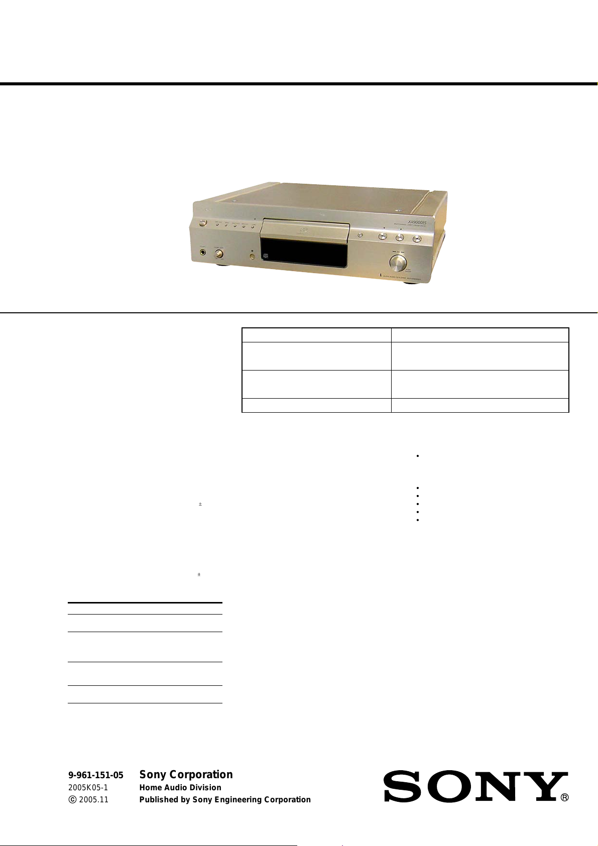
SCD-XA9000ES
SERVICE MANUAL
Ver. 1.4 2005.11
Model Name Using Similar Mechanism NEW
CD Mechanism Type
Base Unit Name
Optical Pick-up Name KHM-230AAA
US Model
Canadian Model
AEP Model
E Model
CDM19JB-DVBU4C (Except AEP: Silver type)
CDM19JB-DVBU4D (AEP: Silver type)
DVBU4C (Except AEP: Silver type)
DVBU4D (AEP: Silver type)
When a super audio CD is played
Playing frequency range 2 Hz to 100 kHz
Frequency response 2 Hz to 50 kHz (−3 dB)
Dynamic range 108 dB or more
Total harmonic distortion rate
Wow and flutter Value of measurable limit ( 0.001 %
When a CD is played
Frequency response 2 Hz to 20 kHz
Dynamic range 100 dB or more
Total harmonic distortion rate
Wow and flutter Value of measurable limit ( 0.001 %
Output connector
ANALOG OUT
DIGITAL (CD)
OUT
OPTICAL*
DIGITAL (CD)
OUT
COAXIAL*
PHONES
*Output only the audio signals of the CD
Jack type
Phono
jacks
Square
optical
output
connector
Coaxial
output
connector
Stereo
phone jack
0.0012 % or less
W. PEAK) or less
0.0017 % or less
W. PEAK) or less
Output level
2 Vrms
(at 50 kilohms)
−18 dBm
0.5 Vp-p
10 mW
Load impedance
Over 10 kilohms
Light emitting
wave length:
( )
660 nm
75 ohms
32 ohms
SPECIFICATIONS
i.LINK section
Pin 4 pins
Transmission speed S200
Transmission protocol A/M transmission protocol
Format (output) Super Audio CD* (DSD PLAIN)
* Conforms to the copy protection technology of DTLA (Revision
1.2).
General
Laser Semiconductor laser
Laser radiant power: 5.47 uW at 650 nm
*These output is the value measured at a distance of about
200mm from the objective lens surface on the optical pick-up.
Power requirements
Power consumption 32 W
Dimensions (w/h/d) 430 × 127 × 387 mm
Mass (approx.) 16.2 kg (35 lbs 12 oz.)
(Maximum data transmission speed
200 Mbps)
2 channel linear PCM (IEC 60958-3)
Sampling frequency: 44.1 kHz
(SA-CD: λ = 650 nm)
(CD: λ = 780 nm)
Emission duration: continuous
Taiwan model:
110 V AC, 60 Hz
US, Canadian models:
120 V AC, 60 Hz
AEP model:
230 V AC, 50/60 Hz
1
(17 × 5 × 15
/4 in.)
incl. projecting parts
Supplied accessories
Audio connecting cord
phono jack × 2 (Red and White) y phono jack × 2 (Red
and White) (3)
phono jack × 1 (Black) y phono jack × 1 (Black) (2)
i.LINK connecting cord (1)
Remote commander RM-SX700 (1)
Size AA (R6) batteries (2)
AC power cord (1)
Plug adapter (1) (US, Canadian models only)
Design and specifications are subject to change without notice.
9-961-151-05 Sony Corporation
2005K05-1 Home Audio Division
C 2005.11 Published by Sony Engineering Corporation
SUPER AUDIO CD PLAYER
SCD-XA9000ES
This appliance is classified as a CLASS 1
LASER product.
The CLASS 1 LASER PRODUCT
MARKING is located on the rear exterior.
r
SAFETY CHECK-OUT
After correcting the original service problem, perform the following safety check before releasing the set to the customer:
Check the antenna terminals, metal trim, “metallized” knobs,
screws, and all other exposed metal parts for AC leakage.
Check leakage as described below.
LEAKAGE TEST
The AC leakage from any exposed metal part to earth ground and
from all exposed metal parts to any exposed metal part having a
return to chassis, must not exceed 0.5 mA (500 microamperes.).
Leakage current can be measured by any one of three methods.
1. A commercial leakage tester, such as the Simpson 229 or RCA
WT -540A. Follo w the manufacturers’ instructions to use these
instruments.
2. A battery-operated AC milliammeter. The Data Precision 245
digital multimeter is suitable for this job.
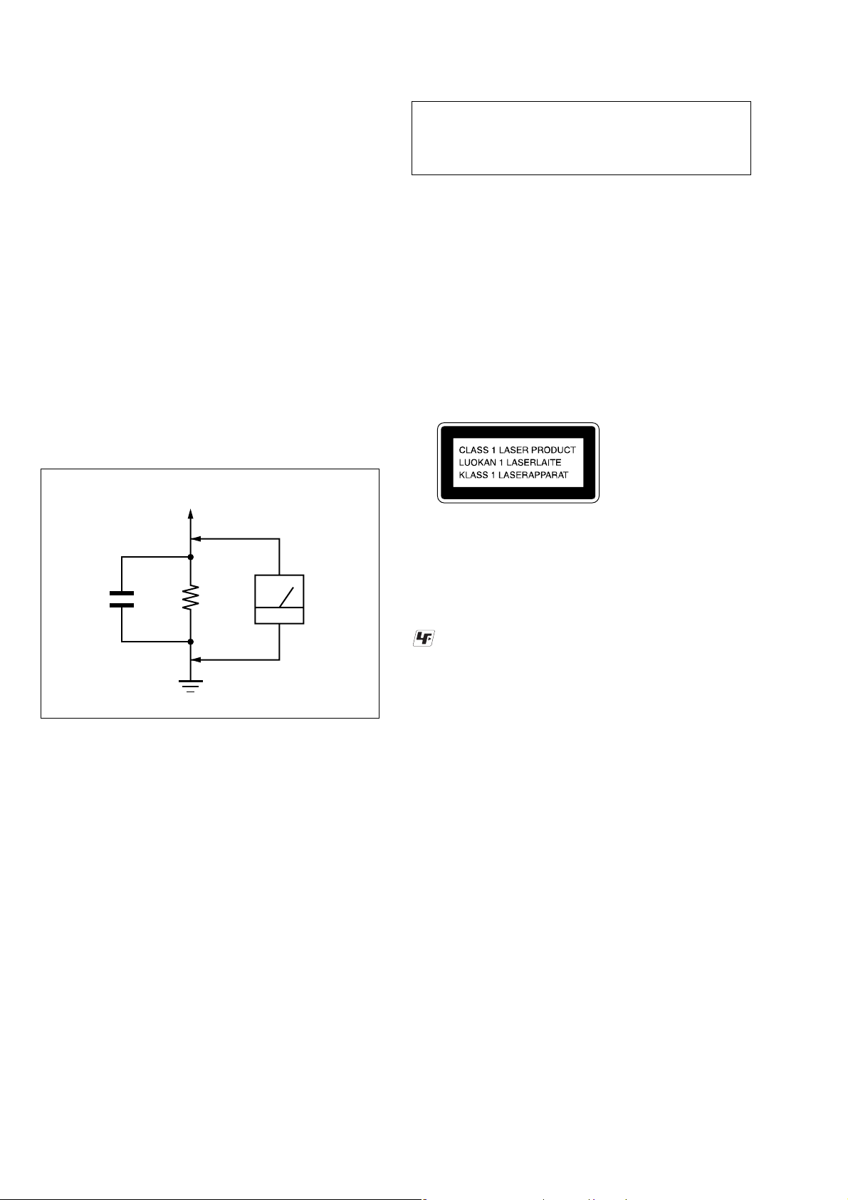
3. Measuring the voltage drop across a resistor by means of a V OM
or battery-operated A C voltmeter . The “limit” indication is 0.75
V, so analog meters must have an accurate low-voltage scale.
The Simpson 250 and Sanwa SH-63Trd are examples of a passive VOM that is suitable. Nearly all battery operated digital
multimeters that have a 2 V AC range are suitable. (See Fig. A)
To Exposed Metal
Parts on Set
CAUTION
Use of controls or adjustments or performance of procedures
other than those specified herein may result in hazardous radiation exposure.
CAUTION
The use of optical instruments with this
product will increase eye hazard.
For the customers in Canada
This Class B digital apparatus complies
with Canadian ICES-003.
AEP model
AC
1.5 k
0.15 µF
Fig. A. Using an AC voltmeter to check AC leakage.
Ω
Earth Ground
voltmete
(0.75 V)
Notes on chip component replacement
•Never reuse a disconnected chip component.
• Notice that the minus side of a tantalum capacitor may be dam-
aged by heat.
Flexible Circuit Board Repairing
•Keep the temperature of the soldering iron around 270 ˚C dur-
ing repairing.
• Do not touch the soldering iron on the same conductor of the
circuit board (within 3 times).
• Be careful not to apply force on the conductor when soldering
or unsoldering.
UNLEADED SOLDER
Boards requiring use of unleaded solder are printed with the leadfree mark (LF) indicating the solder contains no lead.
(Caution: Some printed circuit boards may not come printed with
the lead free mark due to their particular size)
: LEAD FREE MARK
Unleaded solder has the following characteristics.
• Unleaded solder melts at a temperature about 40 °C higher
than ordinary solder.
Ordinary soldering irons can be used but the iron tip has to be
applied to the solder joint for a slightly longer time.
Soldering irons using a temperature regulator should be set to
about 350 °C.
Caution: The printed pattern (copper foil) may peel away if
the heated tip is applied for too long, so be careful!
• Strong viscosity
Unleaded solder is more viscou-s (sticky, less prone to flow)
than ordinary solder so use caution not to let solder bridges
occur such as on IC pins, etc.
• Usable with ordinary solder
It is best to use only unleaded solder but unleaded solder may
also be added to ordinary solder.
SAFETY-RELATED COMPONENT WARNING!!
COMPONENTS IDENTIFIED BY MARK 0 OR DOTTED
LINE WITH MARK 0 ON THE SCHEMATIC DIAGRAMS
AND IN THE PARTS LIST ARE CRITICAL TO SAFE
OPERATION. REPLACE THESE COMPONENTS WITH
SONY PARTS WHOSE PART NUMBERS APPEAR AS
SHOWN IN THIS MANUAL OR IN SUPPLEMENTS PUBLISHED BY SONY.
2
ATTENTION AU COMPOSANT AYANT RAPPORT
À LA SÉCURITÉ!
LES COMPOSANTS IDENTIFIÉS P AR UNE MARQUE 0
SUR LES DIAGRAMMES SCHÉMATIQUES ET LA LISTE
DES PIÈCES SONT CRITIQUES POUR LA SÉCURITÉ
DE FONCTIONNEMENT. NE REMPLACER CES COMPOSANTS QUE PAR DES PIÈCES SONY DONT LES
NUMÉROS SONT DONNÉS DANS CE MANUEL OU
DANS LES SUPPLÉMENTS PUBLIÉS PAR SONY.

TABLE OF CONTENTS
SCD-XA9000ES
Ver. 1.3
1. SERVICING NOTES ............................................... 4
2. GENERAL ................................................................... 10
3. DISASSEMBLY
3-1. Disassembly Flow ........................................................... 13
3-2. Case (Top), Side Plate ..................................................... 14
3-3. Loading Panel Assy......................................................... 14
3-4. Front Panel Section ......................................................... 15
3-5. MAIN Board, Bracket (MAIN) ...................................... 15
3-6. RF Board, Mechanism Deck
(CDM19JB-DVBU4C or CDM19JB-DVBU4D) ........... 16
3-7. Disc T able, Belt, Loading Motor (M1)........................... 16
3-8. Optical Pick-up (KHM-230AAA) .................................. 17
3-9. Base Unit (DVBU4C or DVBU4D)................................ 18
4. TEST MODE.............................................................. 19
5. DIAGRAMS
5-1. Block Diagram – RF/SERVO Section – ........................ 26
5-2. Block Diagram – MAIN Section (1/2) – ....................... 27
5-3. Block Diagram – MAIN Section (2/2) – ....................... 28
5-4. Block Diagram – AUDIO Section (1/2) – ..................... 29
5-5. Block Diagram – AUDIO Section (2/2) – ..................... 30
5-6. Block Diagram – LINK Section – ................................. 31
5-7. Block Diagram
– PANEL/POWER SUPPLY Section – .......................... 32
5-8. Note for Printed Wiring Boards and
Schematic Diagrams ....................................................... 33
5-9. Printed Wiring Boards – SERVO Section – .................. 34
5-10. Schematic Diagram – SERVO Section – ....................... 35
5-11. Printed Wiring Board
– MAIN Board (Component Side) – .............................. 36
5-12. Printed Wiring Board
– MAIN Board (Conductor Side) – ................................ 37
5-13. Schematic Diagram – MAIN Board (1/7) – .................. 38
5-14. Schematic Diagram – MAIN Board (2/7) – .................. 39
5-15. Schematic Diagram – MAIN Board (3/7) – .................. 40
5-16. Schematic Diagram – MAIN Board (4/7) – .................. 41
5-17. Schematic Diagram – MAIN Board (5/7) – .................. 42
5-18. Schematic Diagram – MAIN Board (6/7) – .................. 43
5-19. Schematic Diagram – MAIN Board (7/7) – .................. 44
5-20. Printed Wiring Board – D-OUT Board – ...................... 45
5-21. Schematic Diagram – D-OUT Board – ......................... 45
5-22. Printed Wiring Board
– MOTHER Board (Component Side) – ........................ 46
5-23. Printed Wiring Board
– MOTHER Board (Conductor Side) –......................... 47
5-24. Schematic Diagram – MOTHER Board (1/2) –............ 48
5-25. Schematic Diagram – MOTHER Board (2/2) –............ 49
5-26. Printed Wiring Board – AUDIO FRONT Board – ......... 50
5-27. Schematic Diagram – AUDIO FRONT Board – ........... 51
5-28. Printed Wiring Board – AUDIO SURR Board – ........... 52
5-29. Schematic Diagram – AUDIO SURR Board –.............. 53
5-30. Printed Wiring Board – AUDIO C/SW Board – ............ 54
5-31. Schematic Diagram – AUDIO C/SW Board – .............. 55
5-32. Schematic Diagram – LINK Board (1/2) – ................... 56
5-33. Schematic Diagram – LINK Board (2/2) – ................... 57
5-34. Printed Wiring Board – LINK Board – ......................... 58
5-35. Printed Wiring Boards – PANEL Section – .................. 59
5-36. Schematic Diagram – PANEL Section (1/2) – .............. 60
5-37. Schematic Diagram – PANEL Section (2/2) – .............. 61
5-38. Printed Wiring Board
– A-POWER Board (Component Side) – ....................... 62
5-39. Printed Wiring Boards
– A-POWER (Conductor Side)/IC Boards – .................. 63
5-40. Schematic Diagram – A-POWER/IC Boards – ............. 64
5-41. Printed Wiring Board – D-POWER Board –................. 66
5-42. Schematic Diagram – D-POWER Board – ................... 67
5-43. Printed Wiring Boards – AC/AC SW Boards – ............. 68
5-44. Schematic Diagram – AC/AC SW Boards – ................. 69
5-45. IC Pin Function Description ........................................... 74
6. EXPLODED VIEWS
6-1. Case Section .................................................................... 94
6-2. Front Panel Section-1...................................................... 95
6-3. Front Panel Section-2...................................................... 96
6-4. Bottom Section................................................................ 97
6-5. Board Section-1............................................................... 98
6-6. Board Section-2............................................................... 99
6-7. Chassis Section .............................................................. 100
6-8. Mechanism Deck Section .............................................. 101
6-9. Base Unit Section........................................................... 102
7. ELECTRICAL PARTS LIST .............................. 103
3

SCD-XA9000ES
Ver. 1.4
SECTION 1
SERVICING NOTES
MODEL IDENTIFICATION
– Back Panel –
Part No.
Model Part No.
AEP model 4-247-231-0
US and Canadian models 4-247-231-2
Taiwan model 4-247-231-3
NOTES ON HANDLING THE OPTICAL PICK-UP
BLOCK OR BASE UNIT
The laser diode in the optical pick-up block may suffer electrostatic break-down because of the potential difference generated
by the charged electrostatic load, etc. on clothing and the human
body.
During repair, pay attention to electrostatic break-down and also
use the procedure in the printed matter which is included in the
repair parts.
The flexible board is easily damaged and should be handled with
care.
NOTES ON LASER DIODE EMISSION CHECK
The laser beam on this model is concentrated so as to be focused
on the disc reflective surface by the objective lens in the optical
pick-up block. Therefore, when checking the laser diode emission, observe from more than 30 cm away from the objectiv e lens.
CLEANING OF OPTICAL PICK-UP LENS
In cleaning the lens of optical pick-up, use the air blower.
Never use a cotton swab for cleaning the lens of optical pick-up,
which otherwise causes a trouble.
RESETTING OPERATION AT POWER ON
If the power is turned on with a disc loaded in the set, a sequence
of operation as shown below will be performed.
(The operation varies depending on the type of disc)
Condition: continue mode
[]
[]
[]
(2) SACD (single layer)
1. Sled reverse move (sled in)
2. Disc detect
3. IC setting for SACD
4. Servo error signal offset auto adjustment
5. Spindle kick for LD on
6. LD on
7. Focus search
8. Focus servo on
9. Spindle kick
10. Spindle servo on
11. E-F balance auto adjustment
12. Tracking & sled servo on
13. Focus bias auto adjustment
14. Focus servo gain auto adjustment
15. Tracking servo gain auto adjustment
16. Jump to lead-in area
17. Read TOC
18. Stop
(3) SACD (dual layer)
1. Sled reverse move (sled in)
2. Disc detect
3. IC setting for SACD
4. Servo error signal offset auto adjustment
5. Spindle kick for LD on
6. LD on
7. Focus search
8. Focus servo on (layer 0)
9. Spindle kick
10. Spindle servo on
11. E-F balance auto adjustment (layer 0)
12. Tracking & sled servo on (layer 0)
13. Focus bias auto adjustment (layer 0)
14. Focus servo gain auto adjustment (layer 0)
15. Tracking servo gain auto adjustment (layer 0)
16. Jump to lead-in area
17. Read TOC
18. Focus jump (layer 0tlayer 1)
19. E-F balance auto adjustment (layer 1)
20. Tracking & sled servo on (layer 1)
21. Focus bias auto adjustment (layer 1)
22. Focus servo gain auto adjustment (layer 1)
23. Tracking servo gain auto adjustment (layer 1)
24. Focus Jump (layer 1tlayer 0)
25. Stop
(1) CD
1. Sled reverse move (sled in)
2. Disc detect
3. IC setting for CD
4. Servo error signal offset auto adjustment
5. Spindle kick for LD on
6. LD on
7. Focus search
8. Focus servo on
9. Spindle kick
10. Spindle servo on
11. E-F balance auto adjustment
12. Tracking & sled servo on
13. Focus bias auto adjustment
14. Focus servo gain auto adjustment
15. Tracking servo gain auto adjustment
16. Jump to lead-in area
17. Read TOC
18. Stop
4
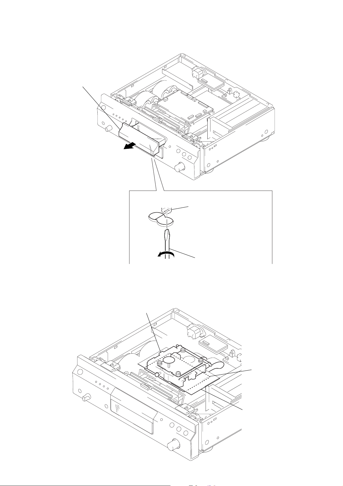
HOW TO OPEN THE DISC TABLE WHEN POWER SWITCH TURNS OFF
loading panel assy
B
2
Draw out the loading panel assy
in the direction of arrow
B
.
SCD-XA9000ES
Ver. 1.3
cover (CAM)
1
Insert a tapering driver in the hole
at the bottom of the unit,
turn the cover (CAM) fully in the
direction of arrow
A
tapering driver
A
.
OPTICAL PICK-UP SERVICE POSITION
Place the insulator on the MAIN board, then install the base unit (DVBU4C or DVBU4D) on it as shown in the figure.
DVBU4C: Except AEP (Silver type)
DVBU4D: AEP (Silver type)
base unit
(DVBU4C or DVBU4D)
MAIN board
insulator
5
SCD-XA9000ES
s
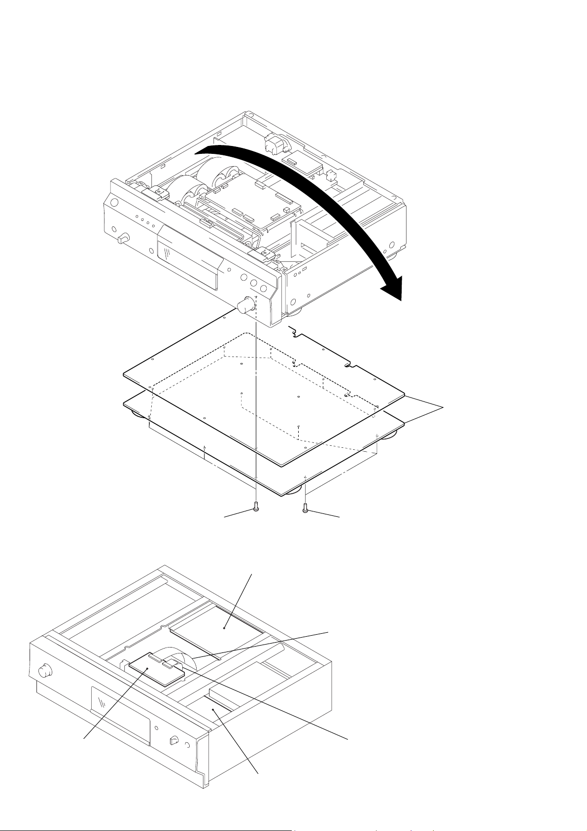
Note: Follow the disassembly procedure in the numerical order given.
D-POWER/POWER BOARDS AND RF BOARD SERVICE POSITION
2
Turn over the set.
– BOTTOM VIEW –
3
eight screws (3 × 8)
power board
4
two bottom plate
3
four screws (3 × 8)
INSTALLATION TWO WIRES (FLAT TYPE) (25/35 CORE)
Note: When the wire (flat type) (35 core) is disconnected
from the RF board, then it is again connected,
disconnect the wire (flat type) (25 core) once,
and reconnect the wire (flat type) (35 core) first.
wire (flat type) (35 core)
6
RF board
wire (flat type) (25 core)
D-power board
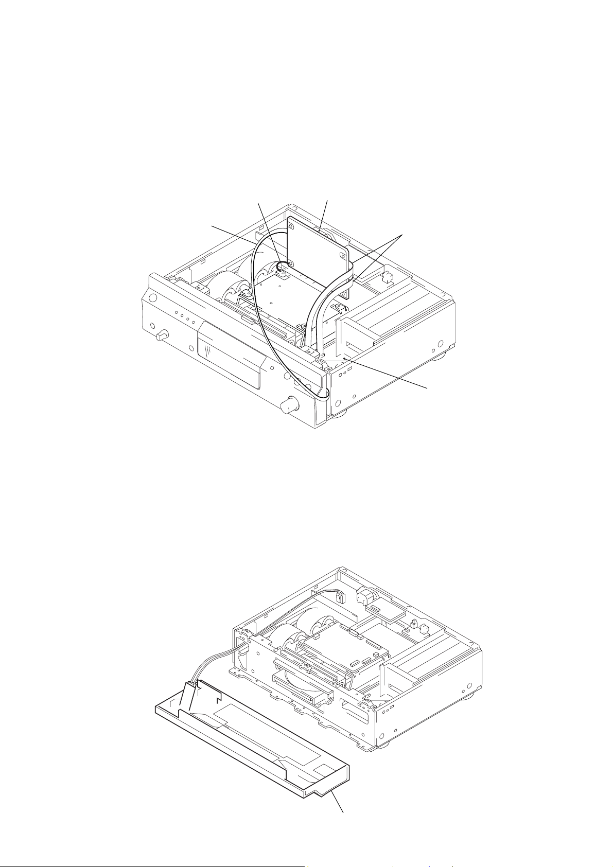
SCD-XA9000ES
MAIN BOARD SERVICE POSITION
In checking the MAIN board, prepare jig (extension cable J-2501-205-A: 1.50 mm Pitch, 7 cores, Length 300 mm/
J-2501-086-A: 1.00 mm Pitch, 19 cores, Length 300 mm).
Note: Be sure to ground the MAIN board with a lead wire when checking it.
connect jig (extension cable J-2501-205-A)
to the main board (CN706) and display
board (CN801).
lead wire
main board
connect jig (extension cable J-2501-086-A)
to the main board (CN701) and mother board (CN301),
main board (CN702) and mother board (CN302).
MOTHER board
FRONT PANEL SECTION SERVICE POSITION
front panel section
7
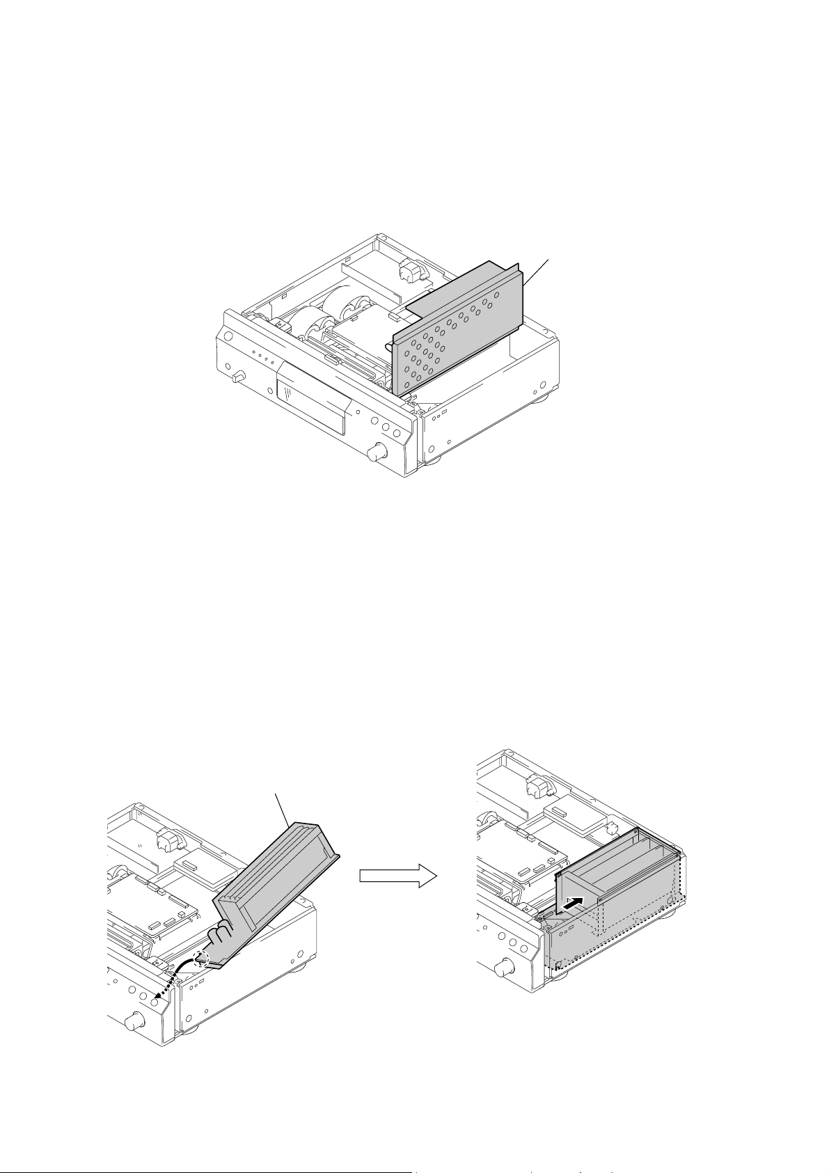
SCD-XA9000ES
k
AUDIO MODULE BLOCK SERVICE POSITION
audio module bloc
NOTE FOR INSTALLATION (AUDIO MODULE BLOCK)
Note: When installing the audio module block, insert the audio module block as shown below.
audio module block
8
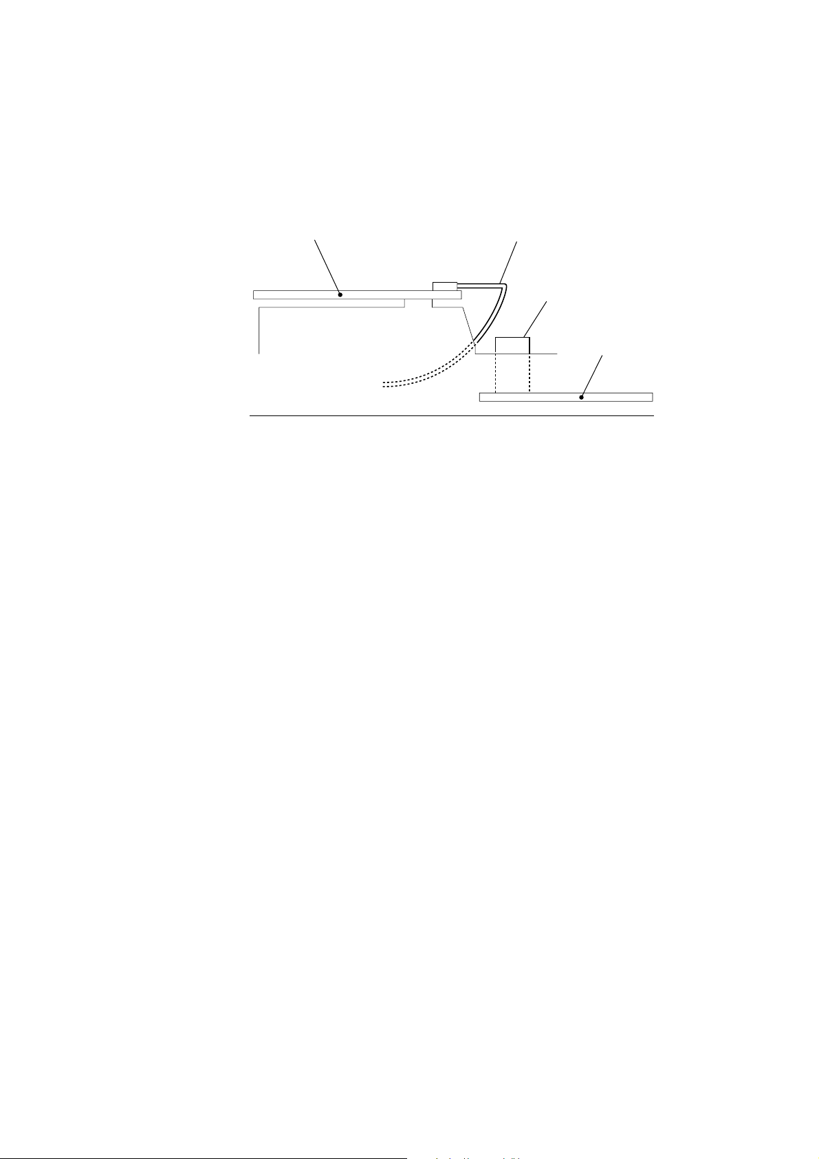
NOTE ON POSITION OF WIRE (FLAT TYPE)
SCD-XA9000ES
FRONT
B
MAIN board
wire (flat type)
heatsink
A-POWER board
Heatsink gets heated up to a high temperature.
Be careful to keep the position of wire (flat type).
9
SCD-XA9000ES
SECTION 2
GENERAL
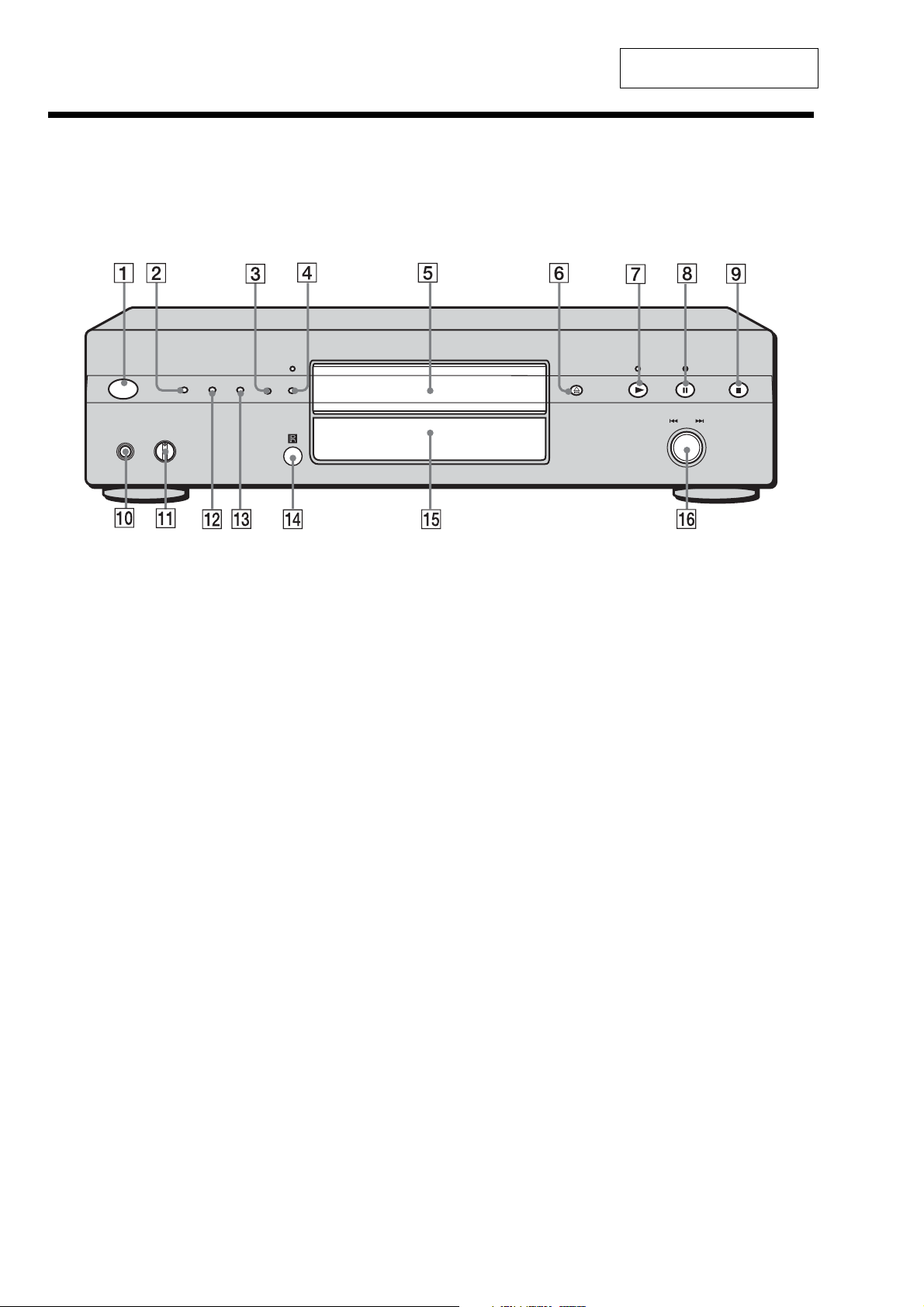
Front Panel Parts Descriptions
This section is extracted from
instruction manual.
POWER
PHONES
TIME/TEXT
PHONE LEVEL
MIN MAX
MENU
MULTI/2CH
SACD/CD
i.LINK
1 POWER switch
Press to turn on the player.
2 TIME/TEXT button
Each time you press the button, the playing time of the
track, the total remaining time on the disc, or TEXT
information appears in the display.
3 SACD/CD button
Each time you press the button while playing back a
hybrid disc, the layer to be played back switches
between the HD (Super Audio CD) layer and the CD
layer.
4 i.LINK button
Each time you press the button, i.LINK function turns
on or off.
AMS
PUSH
ENTER
9 x button
Press to stop play.
0 PHONES
Connect the headphones.
During playback of a Multi-channel Super Audio CD,
the same signal that is output from the ANALOG
5.1CH FRONT L/R jacks is output from the PHONES
jack.
qa PHONE LEVEL
Adjust the headphones volume.
qs MENU
Press to enter the menu.
Press to exit from the menu and return to the normal
display.
i.LINK indicator
Lights up when the i.LINK function is used.
5 Disc tray
Press A OPEN/CLOSE to open/close the disc tray.
6 A OPEN/CLOSE button
Press to open or close the disc tray.
7 N button
Press to start play.
N indicator
Lights up during playback.
8 X button
Press to pause play.
X indicator
Lights up during pause.
10
qd MULTI/2CH button
Press to select the playback area when the 2 channel +
Multi-channel Super Audio CD is loaded.
qf Remote sensor
qg Display window
Shows various information.
qh . AMS > dial (AMS: Automatic Music Sensor)
When you turn the . AMS > dial
counterclockwise by one click, you go back to the
preceding track; when you turn the . AMS >
dial clockwise by one click, you go to the succeeding
track.
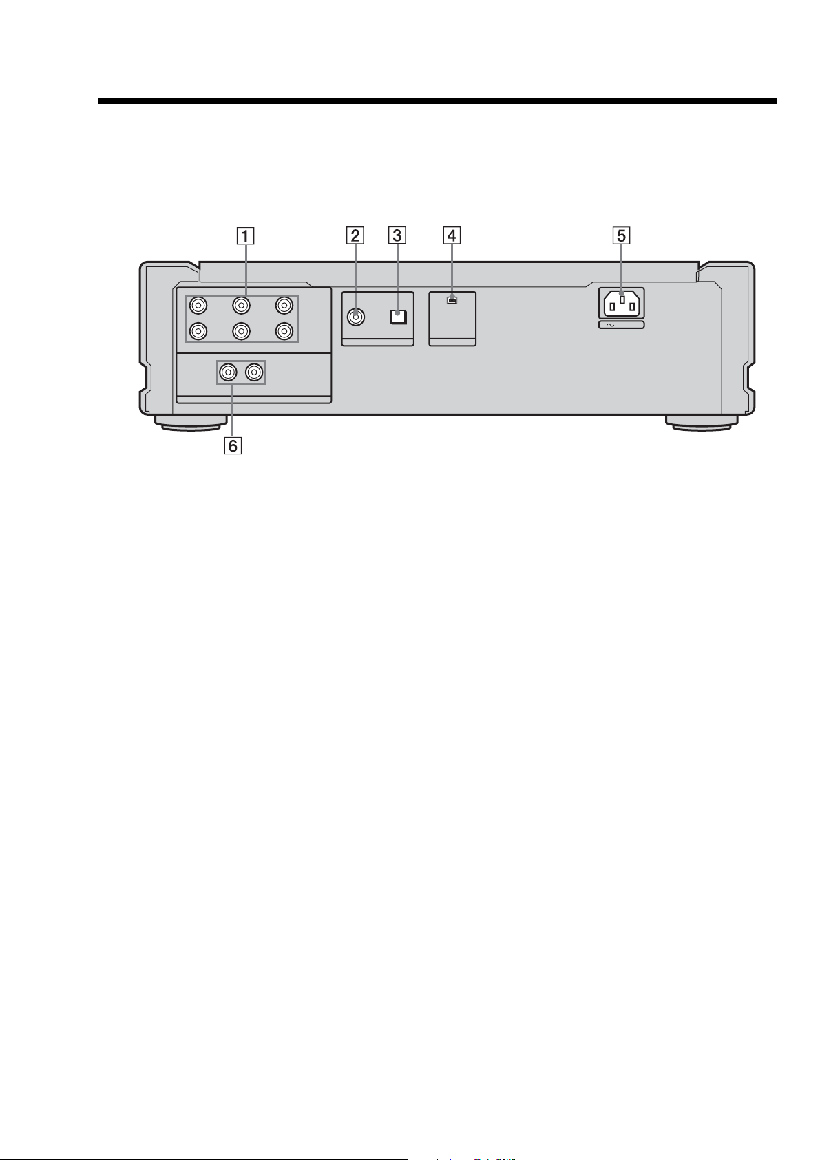
Rear Panel Parts Descriptions
CENTER
L
RR
L
FRONT SURROUND SUB WOOFER
LR
ANALOG
5.1CH OUT
2CH OUT
OUT
DIGITAL(CD)
OPTICALCOAXIAL
AUDIO OUT
i.LINK S200
SCD-XA9000ES
AC IN
1 ANALOG 5.1CH OUT jacks
Connect to an amplifier equipped with the 5.1CH
input jacks (Multi-channel amplifier, AV amplifier,
etc.) using the audio connecting cords.
2 DIGITAL (CD) OUT COAXIAL connector
Connect to an audio component using the coaxial
digital cable.
3 DIGITAL (CD) OUT OPTICAL connector
Connect to an audio component using an optical
digital cable.
4 i.LINK S200 AUDIO OUT jack
Connect to STR-DA9000ES/TA-DA9000ES using the
i.LINK connecting cord.
5 AC IN terminal
Connect the AC power cord.
6 ANALOG 2CH OUT L/R jacks
Connect to an audio component (stereo/2 channel)
using the audio connecting cord.
Note
Only the audio signals of the CD can be output from the
DIGITAL (CD) OUT connectors shown in 2 and 3. Those of the
Super Audio CD cannot be output through DIGITAL (CD) OUT
connectors.
When the i.LINK indicator is lit
No signal is output from all the other jacks (ANALOG 2CH OUT
jacks, ANALOG 5.1CH OUT jacks, PHONES jack, DIGITAL (CD)
OUT jacks).
11
SCD-XA9000ES
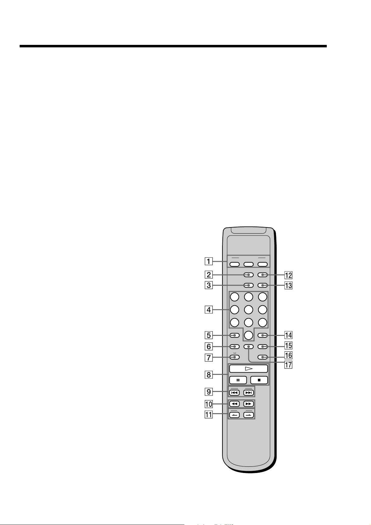
Remote Parts Descriptions
1 CONTINUE button
Press to resume normal play from Shuffle Play or
Program Play.
SHUFFLE button
Press to select Shuffle Play.
PROGRAM button
Press to select Program Play.
2 DISPLAY MODE button
Press to turn the display information off or on.
3 TIME/TEXT button
Each time you press the button, the playing time of the
track, the total remaining time on the disc, or TEXT
information appears in the display.
4 Number buttons
Press to enter the track numbers.
5
i
10 button
Press to locate a track numbered over 10.
6 REPEAT button
Press repeatedly to play all tracks or only one track on
the disc.
7 AyB button
Press to select Repeat A-B Play.
8 H button
Press to start play.
X button
Press to pause play.
x button
Press to stop play.
9 AMS ./> (AMS: Automatic Music Sensor)
buttons
Press to locate a specific track.
0 m/M buttons
Press to locate a portion you want to play within a
track.
qs SACD/CD button
Each time you press the button, ”SACD“ or ”CD“
appears in the display. Select the type of CD you want
to play.
qd MULTI/2CH button
Press to select the playback area when the 2 channel +
Multi-channel Super Audio CD is loaded.
qf ENTER button
Press to decide the selection.
qg CLEAR button
Press to delete a programed track number.
qh LEVEL ADJ button
Press to adjust the output level balance for the Multichannel management function.
qj CHECK button
Press to check the programed order.
PLAY MODE
CONTINUE SHUFFLE
DISPLAY/
MODE
TIME/TEXT
PROGRAM
SACD/CD
MULTI/2CH
123
456
10/0
CHECK
9
CLEAR
LEVEL
ADJ
78
>10 ENTER
REPEAT
BA
qa INDEX >/. buttons
Press to locate a specific point marked with an index
signal when you play a disc that has index signals.
12
AMS
INDEX
SECTION 3
DISASSEMBLY
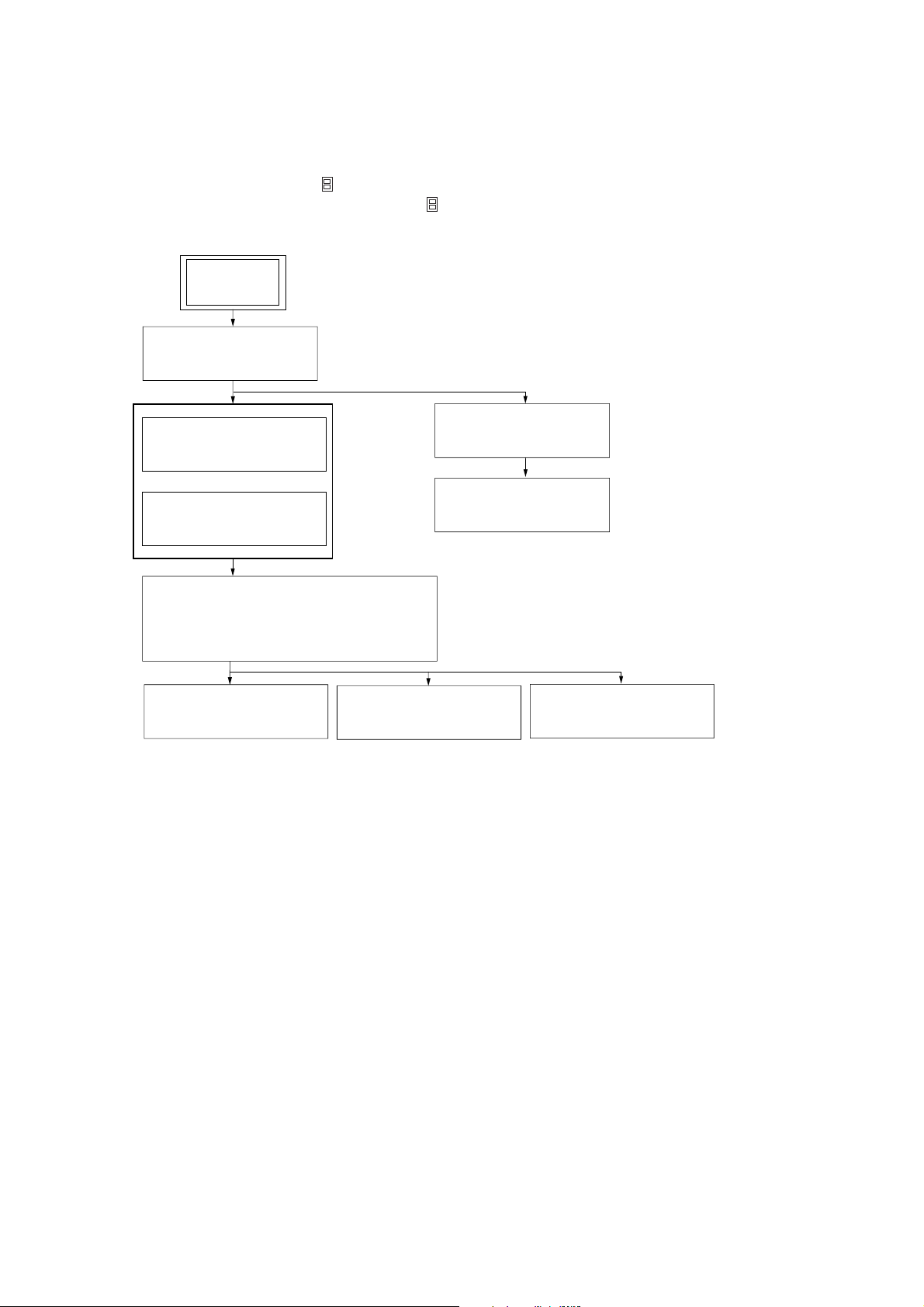
• This set can be disassembled in the order shown below.
3-1. DISASSEMBLY FLOW
Note 1: The process described in can be performed in any order.
Note 2: Without completing the process described in , the next process can not be performed.
SET
3-2. CASE (TOP),
SIDE PLATE
(Page 14)
3-3. LOADING PANEL
3-3. LOADING PANEL ASSY
(Page 14)
ASSY
(Page 14)
SCD-XA9000ES
Ver. 1.3
3-5. MAIN BOARD,
BRACKET (MAIN)
(Page 15)
3-6. RF BOARD,
MECHANISM DECK
(CDM19JB-DVBU4C or CDM19JB-DVBU4D)
(Page 16)
3-7. DISC TABLE, BEL T,
LOADING MOTOR (M1)
(Page 16)
3-8. OPTICAL PICK-UP
3-4. FRONT PANEL
(KHM-230AAA)
(Page 17)
SECTION
(Page 15)
3-9. BASE UNIT
(DVBU4C or DVBU4D)
(Page 18)
13
SCD-XA9000ES
Note: Follow the disassembly procedure in the numerical order given.
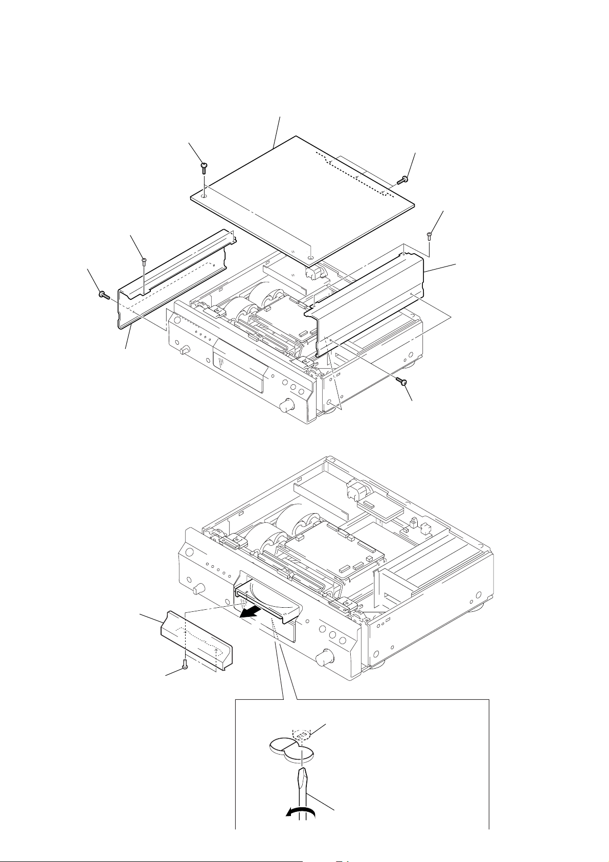
3-2. CASE (TOP), SIDE PLATE
3
2
two screws
(flat head)
4
two screws
(3
×
8)
5
two screws
(flat head)
case (top)
1
three screws
(flat head)
7
two screws
(3
9
×
8)
side plate (right)
6
side plate (left)
3-3. LOADING PANEL ASSY
4
loading panel assy
2
8
two screws
(flat head)
14
3
two screws
(P 3
×
10)
A
cover (CAM)
1
tapering driver
Insert a tapering driver in the hole
at the bottom of the unit,
turn the cover (CAM) fully in the
direction of arrow
A
.
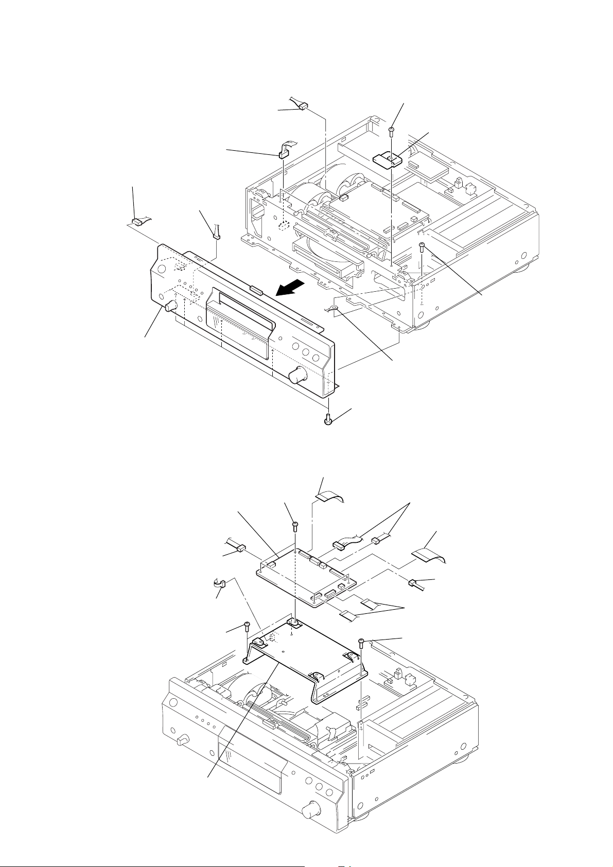
3-4. FRONT PANEL SECTION
)
1
connector
(CN453)
9
connector
(CN994)
0
connector
(CN601)
2
connector
(CN706)
8
5
two screws
(3
×
8)
6
two brackets (F)
SCD-XA9000ES
3
screw
(BVTT 3
×
6)
qa
front panel section
3-5. MAIN BOARD, BRACKET (MAIN)
7
8
main board
6
connector (CN706)
9
connector (CN423)
qa
two screws
(3
×
8)
four screws
(3
×
8)
7
five screws
(3
×
8)
1
wire (flat type) (25 core)
(CN710)
4
harness
5
two connectors
(CN703, 707)
2
4
3
two wires (flat type)
(19 core) (CN701, 702)
0
two screws
(3
×
8)
wire (flat type) (35 core
(CN708)
connector (CN704)
qs
bracket (main)
15
SCD-XA9000ES
r
)
Ver. 1.3
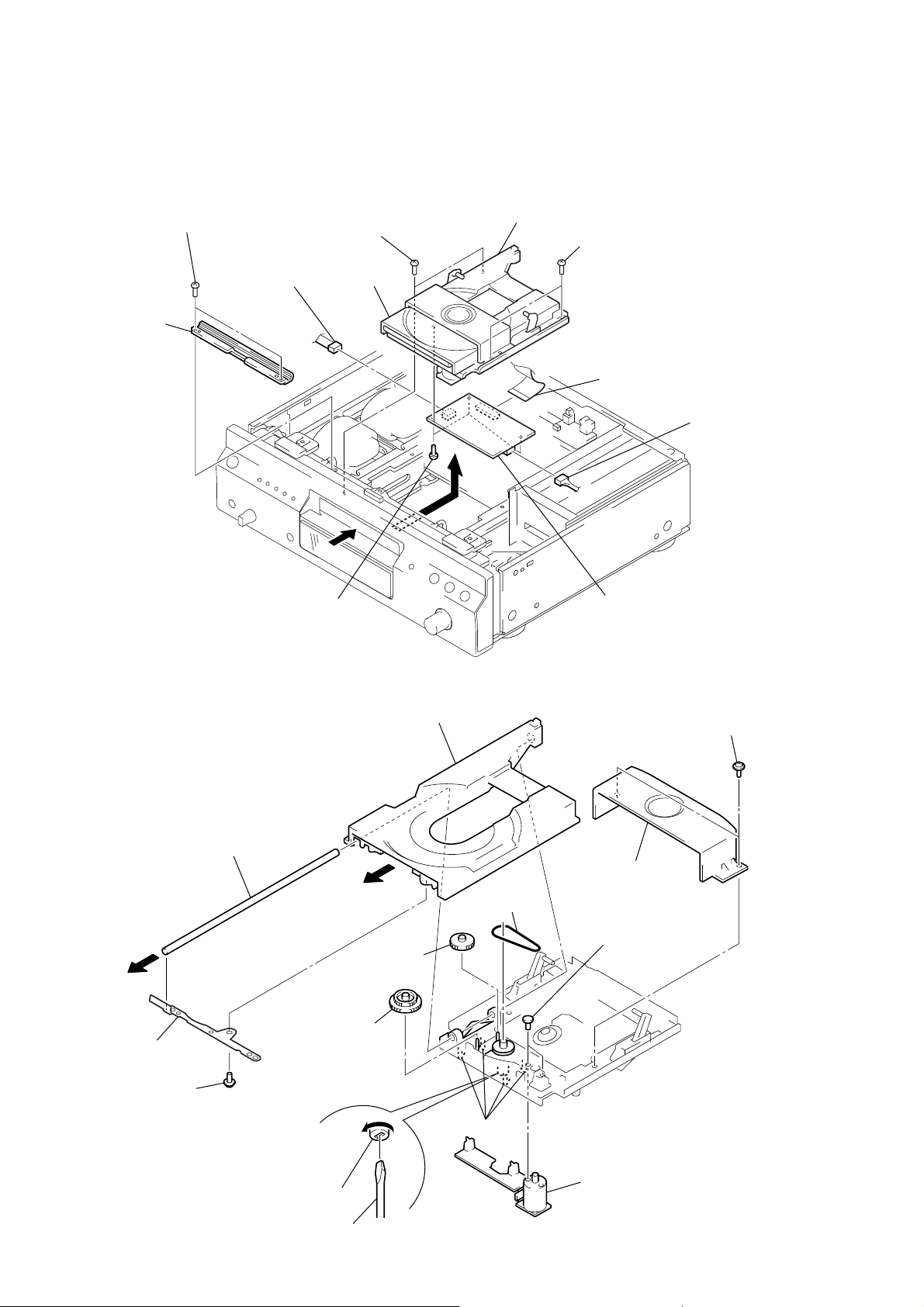
3-6. RF BOARD, MECHANISM DECK (CDM19JB-DVBU4C or CDM19JB-DVBU4D)
CDM19JB-DVBU4C: Except AEP (Silver type)
CDM19JB-DVBU4D: AEP (Sivler type)
qs
mechanism deck
(CDM19JB-DVBU4C or CDM19JB-DVBU4D)
5
two screws (3 × 8)
7
wire (flat type) (25 core)
(CN003)
6
3
bracket
(guide wire)
2
two screws
(3
×
8)
9
connector
(CN001)
4
two screws (3 × 8)
disc table
8
connecto
(CN002)
1
Push the disc table in the
direction of arrow
A
.
0
three screws
(BVTP2.6
A
×
8)
3-7. DISC TABLE, BELT, LOADING MOTOR (M1)
9
8
guide bar (main)
4
qa
gear (C)
7
disc table
qs
belt
qa
RF board
2
holder (A. P.) assy
qd
two screws
(P3
1
×
3)
two screws
(BVTT M3 S
16
6
bracket
(loading panel)
5
tapping screw
3
Insert a tapering driver in the
hole of the cover (CAM) and
turn fully in the direction of
arrow
A
.
cover (CAM)
0
gear (P)
A
taper driver
qf
four claws
qg
loading motor (M1)
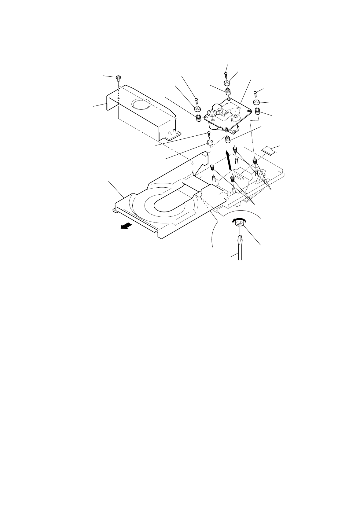
3-8. OPTICAL PICK-UP (KHM-230AAA)
2
holder (A. P.) assy
7
stopper
4
Draw out the disc table fully
in the arrow
B
direction.
7
stopper
7
stopper
7
stopper
0
optical pick-up (KHM-230AAA)
6
screw
(BVTP2.6
×
8)
6
screw
(BVTP2.6
×
8)
6
screw
(BVTP2.6
×
8)
6
screw
(BVTP2.6
×
8)
9
insulator
9
insulator
9
insulator
9
insulator
5
wire (flat type) (25 core)
(CN003)
8
qa
two cone type coil spring (230)
qa
two cone type coil spring (230)
3
Insert a tapering driver in the
hole of the cover (CAM) and
turn fully in the direction of
arrow
A
.
cover (CAM)
taper driver
A
B
1
two screws
(BVTT M3 S)
SCD-XA9000ES
17
SCD-XA9000ES
)
Ver. 1.3
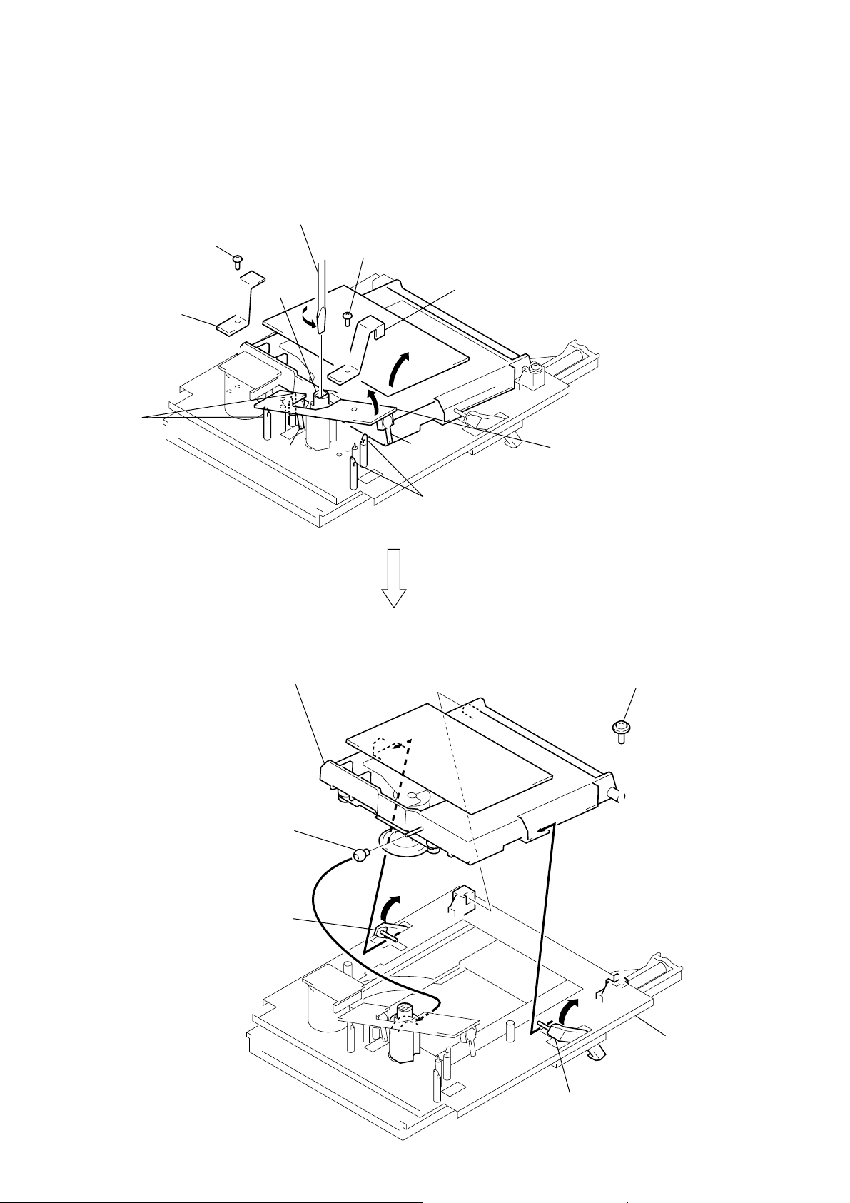
3-9. BASE UNIT (DVBU4C or DVBU4D)
DVBU4C: Except AEP (Silver type)
DVBU4D: AEP (Sivler type)
7
Insert a taper driver into the cover (CAM),
and rotate in the arrow
the base unit (DVBU4C or DVBU4D) in the arrow
C
direction. (Chuck release state)
×
6)
cover (CAM)
B
1
two claws
6
limiter (R)
5
screw
(BVTT3
B
direction to raise
3
screw
(BVTT3
C
A
×
6)
4
limiter (L)
S001
9
Raising the stable lock (L/R) assy simultaneously
in the arrow
(DVBU4C or DVBU4D) from the chassis (outseat).
Note: The stable lock (L/R) assy will attempt to
return in the reverse direction of arrow
by a spring force. Therefore, take care not
to break the shaft of stable lock (L/R) assy
when removing the stable lock (L/R) assy
from the base unit (DVBU4C or DVBU4D).
D
direction, remove the base unit
D
0
roller (L)
S002
1
two claws
2
Up the SWITCH board in the
direction of arrow
Note: Take care not to break the shaft of
the switch (S001, S002) when raising
the SWITCH board.
8
screw (PTPWH3 × 8)
A
.
18
stable lock (R) assy
D
D
chassis (outseat
stable lock (L) assy
SECTION 4
TEST MODE
SCD-XA9000ES
In this set, various checks are automatically performed by executing
the commands in the test mode.
Note: This set makes adjustment e very optical pick-up and stores its result
in the EEPROM (IC903) on the MAIN board. Accordingly, if a
combination of optical pick-up and EEPROM is changed, be sure
to perform 4-3. SET CHECK. Also, perform 4-1. IC INTERFACE
CHECK, 4-2. DISPLA Y CHECK, and 4-6. WAVEFORMS CHECK.
Disc for Test Mode
Various checks of this set require the following discs.
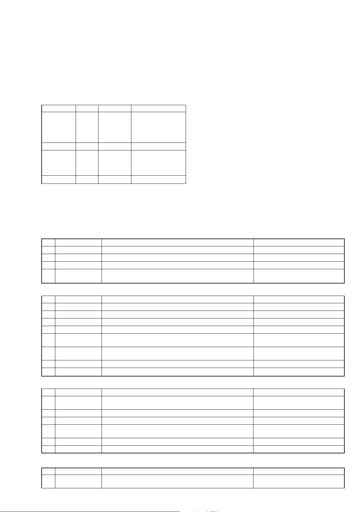
Model Type *1 Category Application
MODEL
SATD-S5
(J-2501-215-A) SL
SATD-S4 Optical waveform check
(J-2501-184-A)
Not specified DL 12 cm disc Operation check
PATD-012
(4-225-203-01)
YEDS-18 Reference disc
(3-702-101-01)
Not specified HYBRID 12 cm disc Operation check
CD
12 cm disc
Reference disc
12 cm disc
Adjusted value check,
Operation check,
Adjusted value check,
Operation check,
Optical waveform check
Setting Method of Test Mode
Turn the [POWER] button on while pressing the [ AMS ]
dial and the [MENU] button. Release the [MENU] button and the
lL
[ AMS ] dial in this order when “DIAG MODE” is displayed
on the fluorescent indicator tube.
Releasing Method of Test Mode
To release the test mode, turn the [POWER] switch off.
Selection/Entry of Test Mode
To select and enter the “DIAG MODE”, operate as follows.
1. Rotate the [ AMS ] dial to select the menu, and press
2. The test is switched on or off alternately each time the
3. To return to the pre vious step, rotate the [ AMS ] dial
*1 SL: Single Layer
DL: Dual Layer
Test Mode Command List
The contents of test mode are as follows.
Note: Wrong operation in the test mode causes a trouble, thus requiring extreme care.
lL
lL
lL
the [ AMS ] dial to enter.
lL
[ AMS ] dial is pressed.
lL
to select the desired item, and press the [ AMS ] dial
l
L
to enter.
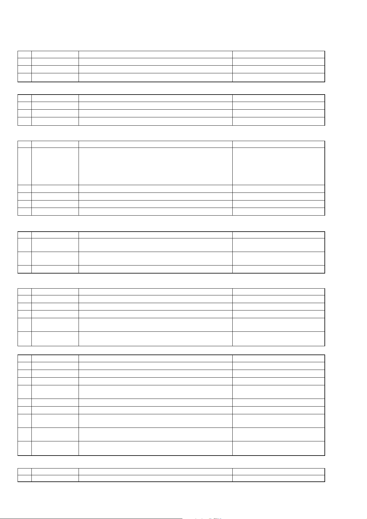
LINE command (0X): Use mainly for a manufacturing line.
No. Name Description Remarks
00 RFAmp Read Each register set value of the IC001 (RF AMP) is displayed via RS-232C Not used for the servicing
05 DSP MON1 XUGF, XPCK, C2PO outputted from IC509 (CD DSP) Not used for the servicing
06 DSP MON2 MNT0, MNT1, MNT2, MNT3 outputted from IC509 (CD DSP) Not used for the servicing
07 DSP MON3 RFCK, XPCK, XROF, GTOP outputted from IC509 (CD DSP)
Electrical measurement,
CD CLV jitter measurement
STANDARD command (1X): Use when the servo is applied by manual operation.
No. Name Description Remarks
12 LD ON/OFF The laser diode is turned on or off On or off are switched alternately
13 SPIN ON/OFF The spindle motor is rotated with the regulated voltage On or off are switched alternately
14 FSRV ON/OFF The focus servo is turned on or off On or off are switched alternately
15 TSRV ON/OFF The tracking servo is turned on or off On or off are switched alternately
16 CLV ON/OFF
17 SSRV ON/OFF
18 ALL SRV ON All servos are turned on
19 ALL SRV OFF All servos are turned off Stop command in the test mode
The spindle SLV servo is turned on or off
Focus and tracking servos must be already turned on
The sled servo is turned on or off
Focus, tracking and spindle servos must be already turned on
On or off are switched alternately
On or off are switched alternately
FOCUS command (2X): Focus related. (All servos must be already turned on (except command 21))
No. Name Description Remarks
21 FSRCH ON/OFF
22 F-BIAS UP Increase focus bias Focus bias value
23 F-BIAS DOWN Decrease focus bias Focus bias value
24 ADJ FCSBIAS
25 FGAIN UP/DW The focus servo gain is switched between normal and down Normal or down are switched alternately
27 FOCUS AGC The focus servo gain is adjusted automatically
The continuous vertical motion of the optical pick-up lens is turned on or Avoid a long-time use
off On or off are switched alternately
The focus bias is adjusted automatically
Both + and - directions are searched to search for best jitter point
OFFSET (PI, FE, TE) command (3X): Adjusts the offset of PI, FE and TE signals.
No. Name Description Remarks
31 PI/FE OFSET
Adjusts the offset of PI, FE and TE signals TE offset adjustment is executed for the CD
This adjustment must be executed after 61 DISC DETECT only
19
SCD-XA9000ES
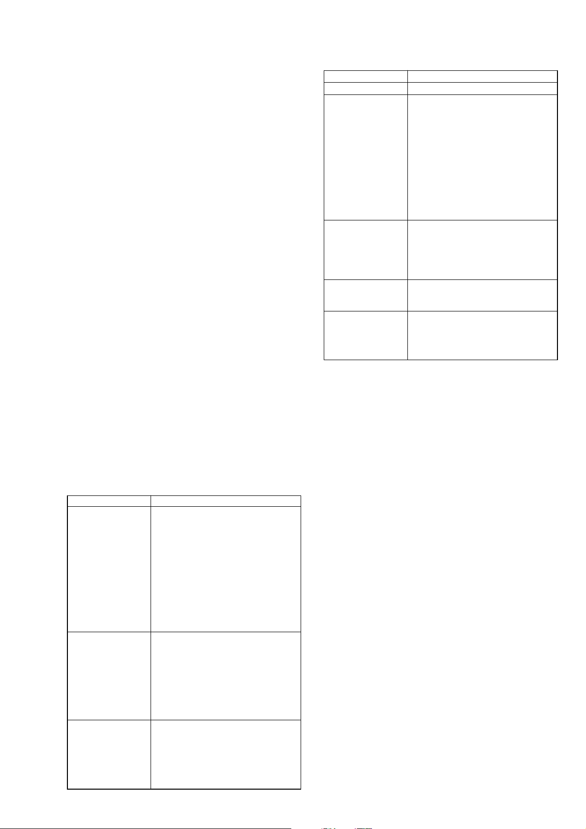
TRACKING command (4X): Tracking servo related.
No. Name Description Remarks
41 TGAIN NM/UP The tracking servo gain is switched between normal and up Normal or up are switched alternately
44 ADJ TRK DSP The traverse AGC and E-F balance adjustment is performed
45 TRACKING AGC The tracking servo gain is adjusted automatically
SEARCH command (5X): Track search related. (Nos. 51 through 53 are not used for the servicing.)
No. Name Description Remarks
51 1-TRCK JUMP One-track jump is performed
52 FINE SEARCH Fine search is performed
53 M-TRCK MOVE M-track movement is performed
DISC DETECT command (6X): Disc type check related.
No. Name Description Remarks
Disc type check is executed
Display after judgment
61 DISC DETECT
62 CD SETTING Enter disc type CD setting CD forced setting
63 SL SETTING Enter disc type SL setting SL forced setting
64 DL SETTING Enter disc type DL setting DL forced setting
6F Download Not used for the servicing
DSKMOD CD: Judged as CD Refer to how to apply servo by manual
DSKMOD SL: Judged as SACD (SL) operation (See page 21)
DSKMOD DL: Judged as SACD (DL)
DSKMOD HYB: Judged as HYBRID
LASER command (7X): Laser of optical pick-up related.
No. Name Description Remarks
7A ADDTIME CD
7B ADDTIME HD
7C FJUMP TEST Not used for the servicing
Cumulative light emission time of the laser for CD is displayed
(Initialized by 8D command)
Cumulative light emission time of the laser for SACD is displayed
(Initialized by 8D command)
TOOLS command (8X): Performs aging, reads adjusting parameters, etc.
No. Name Description Remarks
81 VERSION Firmware version is displayed Example: Ver 1.00
83 TRAY AGING Tray open-close aging is performed Not used for the servicing
87 DISP ADJ DT Automatic adjusting parameters are displayed via RS-232C Not used for the servicing
8D SETUP MODE
8F SETUP U/CA
Set to factory shipping mode Set when repair completed
PLAY MODE, etc. are initialized (AEP model only) Refer to 4-5. SHIPPING MODE (See page 24)
Set to factory shipping mode Set when repair completed
PLAY MODE, etc. are initialized (US and Canadian models only) Refer to 4-5. SHIPPING MODE (See page 24)
QA command (9X)
No. Name Description Remarks
91 FJUMP CHECK The focus jump is checked Not used for the servicing
92 SET CHECK The set is checked Refer to 4-3. SET CHECK (See page 22)
93 WATER MARK Not used for the servicing
94 SET AGING
95 FJMP CHK BU The focus jump is checked (for jig) Not used for the servicing
9A MIRR MES MIRR signal offset measurement Not used for the servicing
9C BU DENCHO
9D PLAY&RFD ON
9E RFD ON/OFF
The set aging is performed
Repeat by the specified number of times or until an error occurred
The S curve waveform, traverse waveform, and RF waveform can be Refer to 4-6.WAVEFORMS CHECK
checked successively (See page 24)
SACD playback, RFD output
SACD jitter measuring mode
RFD output is turned on or off
SACD jitter measuring mode
Not used for the servicing
Not used for the servicing
Not used for the servicing
IC command (AX)
No. Name Description Remarks
A0 IC SELF CHK Each IC and its communication are checked Normal or up are switched alternately
20
SCD-XA9000ES
How to Apply Servo by Manual Operation
In analyzing failures of the set, the servo may be applied by manual
operation. To apply servo in the test mode, use the following
method.
1. After setting the test mode, rotate the [ AMS ] dial to
select a command, and press the [ AMS ] dial to enter .
lL
lL
2. “61 DISC DETECT” (Disc type check)t“18 ALL SR V ON”
(All servos on + auto adjustment)
3. If applying servo while checking the condition one by one,
“61 DISC DETECT” (Disc type check)t“31 PI/FE OFSET”
(Offset automatic adjustment)t“14 FSRV ON/OFF” (Focus
servo on)t“16 CLV ON/OFF” (CLV servo on) t“44 ADJ
TRK DSP ” (E-F balance adjustment)t“15 TSR V ON/OFF”
(Tracking servo on)t“17 SSRV ON/OFF” (Sled servo
on)t“24 ADJ FCSBIAS” (Focus bias adjustment)t“27
FOCUS AGC” (Focus auto gain adjustment)t“45
TRACKING AGC” (Tracking auto gain adjustment).
Note: 1. On and off are alternately switched in the same command.
2. For a stop, select “19 ALL SR V OFF” and press the [ AMS ]
dial.
lL
4-1. IC INTERFACE CHECK
The communication between microcomputer and main ICs is
checked.
Checking Method:
1. After setting the test mode, rotate the [ AMS ] dial to
select “A0. IC SELF CHECK” and press the [ AMS ]
lL
lL
dial to enter.
2. A checking will start automatically. (Checking time is about 3
seconds)
3. At successful completion of check, “IC CHECK OK” is displayed. In this case, no error exists in the IC interface.
Note: The check mentioned above tests the communication from micro-
computer to main ICs. Even if the check successfully finished, the
IC to be checked is not always normal. Consider it for reference
only.
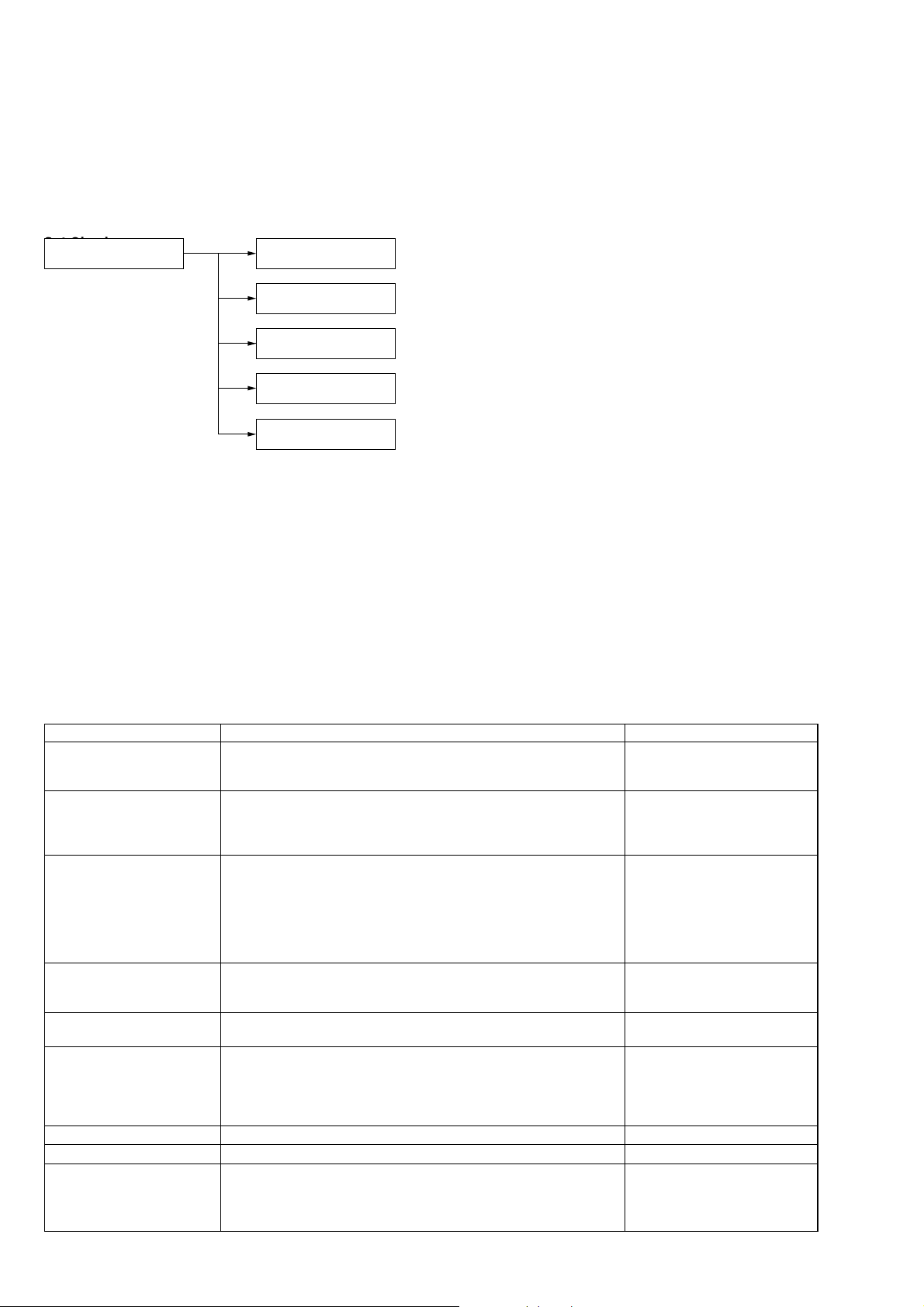
4. In case of an IC communication error, the following display
will be given during the checking. Possible causes of error are
as listed below.
Error display Causes (typical example)
EEPROM ERROR 1. IC903 (EEPROM) is faulty
SAMBA DRAM ERR 1. IC808 (D-RAM) is faulty
(DSD decoder is also 2. IC801 (DSD decoder) is faulty
checked) 3. 768fs (33.8688 MHz) is not present to
RF AMP ERROR 1. IC001 (RF AMP) is faulty
SD BUS ERROR 1. IC701 SD bus and IC801 AV decoder
AUDY ERROR 1. IC802 and IC803 (SD-RAM) are faulty
IC801 pin qa (MCKI)
Same as cause 3 of DVD DEC. ERROR
4. IC801 pin 9 (XRST) does not go “H”
• IC901 pin q; (XDIS IO) does not go “H”
• IC904 (PLD) is faulty
5. Faulty communication line between
IC801 and IC808
•Data line, address line, WE, etc.
6. D904 (1SS367) is faulty
D+3.3V is not present to IC808
2. Loose connection between CN708 on
MAIN board and CN005 on RF board,
or FFC disconnection
CN708 pin ql (CLK RF), pin w; (DATA
RF) and pin wa (SDEN) must be checked
interface is faulty
2. IC812 to 814 are faulty
2. Faulty communication line between
IC802 and IC901
3. Faulty communication line between
IC802 and IC803 (SD-RAM)
Causes Common to Each IC:
1. Faulty communication line between microcomputer and each
IC.
Disconnected patterns, floating series resistors, bridge, etc.
2. Faulty IC supply voltage.
Particularly, check D+3.3V voltage.
3. Faulty microcomputer communication port to each IC
Note: In case of more than two errors, the error display is switched over
one after another, thus making the reading difficult.
In such a case, press again the [ AMS ] dial to make a
recheck for error reading.
lL
Error display Causes (typical example)
DVD DEC. ERROR 1. IC701 (SACD decoder) is faulty
2. IC701 pin <znv (XRST) does not go “H”
• IC901 pin q; (XDIS IO) does not go “H”
• IC904 (PLD) is faulty
3. 768fs (33.8688 MHz) is not present to
IC701 pin <znm (XTAL)
• IC811 (3-multiplying circuit) is faulty
• Clock signal 256fs is not sent from
MOTHER board (CN702 pin 4)
• CN702 pin 1 (GND) and pin 3
(+3.3V-D) are open or shorted
• CN701, 702 and FFC connection is loose,
or FFC is disconnected
DVD DRAM ERR 1. IC706 (D-RAM) is faulty
2. IC701 pin <znv (XRST) does not go “H”
• IC901 pin q; (XDIS IO) does not go “H”
• IC904 (PLD) is faulty
3. Faulty communication line between
IC701 and IC706
•Data line, address line, WE, etc.
4. D903 (1SS367) is faulty
D+3.3V is not present to IC706
CD DSP ERROR 1. IC509 (CD DSP) is faulty
2. 768fs (33.8688 MHz) is not present to
IC509 pin ua (XTAL)
Same as cause 3 of DVD DEC. ERROR
3. IC509 pin 2 (XRST) does not go “H”
• IC901 pin q; (XDIS IO) does not go “H”
• IC904 (PLD) is faulty
4-2. DISPLAY CHECK
Checking Method:
1. Short the BP (TEST MODE) on the DISPLAY board, then
press the [POWER] button to turn on the power.
2. All segments of fluorescent indicator tube will automatically
light up, and therefore check that there is no chipped character.
3. The “Remocon Check” will be displayed after the segment
check finished successfully, then press a proper key on the
remote commander and therefore check that there is reaction
to remote commander.
4. After “Key&Led Check” is displayed, press the key on the
display one by one. If all key on the display is pressed, LED
and segments of fluorescent indicator tube except numbers of
calendar will light up, then “Jog Dial-Check” will be displayed.
5. After “Jog-Dial Check” is displayed, the numbers of calendar
will be displayed from 1 to 15 each time the [ AMS ]
lL
dial is rotated clockwise.
6. After display up to 15, the numbers of calendar will
disappear in order each time the [ AMS ] dial is
lL
rotated counterclockwise.
7. “!%%TEST-END!!%” will be blinked when all are cleared ,
and display check is completed.
21
SCD-XA9000ES
4-3. SET CHECK (AUTOMATIC VARIOUS MEASUREMENTS)
The operational stability of the set is checked. The check and OK/NG judgment are performed automatically.
Note: In the set check using the CD, besides a checking, the MIRR time used for the disc check is measured every optical pick-up, and from the measured
result, the threshold value is calculated and it is stored in the EEPROM (IC903) on the MAIN board. Accordingly, if a combination of optical pickup and EEPROM is changed (for example, the optical pick-up or MAIN board is replaced), be sure to perform the set check using the following CD.
As the data stored in the EEPROM are overwritten every set check, retry if failed. For the set check using the SACD, only checking is made.
Set Check
92. SET CHECK AUTO CHECK SP?
AUTO CHECK?
DISP RESULT S?
DISP RESULT F?
CHECH END?
The set check is executed to judge OK or NG.
(For the CD, the threshold value is stored in the EEPROM)
The set check of measurement only is executed.
The measured result is displayed via RS-232C.
The measured result is displayed on the fluorescent indicator tube.
The set check is finished.
CD and SACD (SL) Disc Operation Check
Checking method:
1. After setting the test mode, rotate the [ AMS ] dial to select “SET CHECK” and press the [ AMS ] dial to enter.
2. Upon display of “AUTO CHECK SP?”, further press the [ AMS ] dial.
lL
lL
lL
3. The tray will open automatically, and then set the test disc*1 of CD or SACD.
4. With the “DISC IN&JOG ON” displayed, press the [ AMS ] dial, and the check will be executed automatically.
lL
5. “SPEC OK!” will be displayed if the measured result is within the specification. Faulty item name and the measured result will be
displayed if any measured item is NG.
6. After that, “AUTO CHECK SP?” will be again displayed, and then rotate the [ AMS ] dial to select “CHECK END?”. Further,
press the [ AMS ] dial, and the test mode selection display will be back, and then press the [OPEN/CLOSE ] button and take
lL
lL
A
the test disc out.
*1 Use PATD-012 or YEDS-18 for CD, and SATD-S5 or SATD-S4 for SACD (SL). Using another disc will result in a checking failure.
Measured Items:
Items Description Remarks
RF/VC/FE/TE (ORG) RF (8 bit data in hex notation) RF: A0h
RF/VC/FE/TE (ADJ)
PI/TRVS PP (ORG/ADJ) TRVS PP (ORG): Traverse level before level correction (AGC) Traverse level conversion
PIOR/CCR/TRCR CCR: Set value of FE offset coarse adjusting register
FOCUS/TRK GAIN
FBIAS/TRVSC/TRCR2/CFR
PSP AMPLITUDE SACD only
1-LAST TRK SEEK (msec) Average seek time from first track to last track of disc
ERROR RATE For CD: Average value/Maximum value of C1 and C2
Offset values before RF (PI), VC, FE, TE signal offset adjustment At offset 0
VC, FE, TE (9 bit data in hex notation) VC, FE, TE: 00h
Offset values after RF (PI), VC, FE, TE signal offset adjustment VC offset is not adjusted
(Less than ORG value if offset correction is normal) (Measurement only)
RF (8 bit data in hex notation) Also, for SACD, the TE offset is
VC, FE, TE (9 bit data in hex notation) not measured and adjusted
PI (ORG): PI value at disc type check (decimal data) PI level conversion
PI (ADJ): PI value after PI offset adjustment Read value × 12.9mV
TRVS PP (ADJ):Traverse level after level correction (AGC)
PIOR: Set value of PI offset coarse adjusting register Registers in RF amplifier
TRCR: Set value of TE offset coarse adjusting register
Auto gain adjusted values of focus and tracking servos
(8 bit data in hex notation)
FBIAS: Focus bias set value (9 bit data in hex notation)
TRVSC: Traverse center value (9 bit data in hex notation)
TRCR2: Set value of E-F balance coarse adjusting register
CFR: Set value of traverse level adjusting register
Error rate measurement
For SACD: Average value/Maximum value of PO, PI1 and PI2
(read value at microcomputer A/D) (decimal data)
(decimal data) Read value × 12.9mV
(decimal data) 12.9mV=3.3V ÷ 256 (8 bit)
TRCR2 adjusts the E-F gain
balance and used for CD only
(Fixed to 06 for SACD)
TRCR2 and CFR are registers in
RF amplifier
For the CD, Measure for 7 sec at track
No.5
For the SACD, calculation from 100block data at track No.5
22
SCD-XA9000ES
Specified Value:
Specified value used for OK/NG judgment when executing 92. SET CHECKtAUTO CHECK SP?
Measured Items Specified value
RF AVRG (ADJ) 8Ch to ABh
VC AVRG (ADJ) 1F7h to09h
FE AVRG (ADJ)
TE AVRG (ADJ) 1E2h to 1Eh
TRVS PP (ADJ) 45h to 73h
FCS GAIN 10h to 60h
TRK GAIN 10h to 60h
ERROR RATE C2 0
PSP AMPLITUDE (SACD only) 1000 to 4000
1-LAST TRK SEK 3500 or less
Note: The specified values attached with “h” are hexadecimal numbers, and others are decimal numbers.
RF, VC, FE, and TE measured values are hexadecimal data with positive and negative signs. When comparing the measured
value with the specified value, refer to the following.
(1) CD 1EEh to 12h
(2) SACD 1F1h to 0Fh
(1) CD
(2) SACD
C1 20 or less
PI1 NUM 100 or less
PI1 FRAME 5 or less
Hexadecimal (hex) display 9 bit data
FF 011111111 (+255)
FE 011111110 (+254)
01 000000001 (+1)
00 000000000 (0)
1FF 111111111 (-1)
101 100000001 (-255)
100 100000000 (-256)
MAX
(+) Side
0
(-) Side
MIN
Hexadecimal (hex) display 8 bit data
7F 01111111 (+127)
7E 01111110 (+126)
02 00000010 (+2)
01 00000001 (+1)
00 00000000 (0)
FF 11111111 (-1)
FE 11111110 (-2)
81 10000001 (-127)
80 10000000 (-128)
23
SCD-XA9000ES
e
4-4. SACD (DL) DISC OPERATION CHECK
(• Perform as necessary)
This checking performs the focus jump using a DL disc, which is
a dual-layer HD disc, to verify the stability of the set.
A set of layer 0 most-outside track access (only once)tone-second
tracetfocus jump (layer 0t1)tone-second tracetfocus jump
(layer 1t0) are repeated 5 times.
Checking Method:
1. After setting the test mode, rotate the [ AMS ] dial to
select “91 FJUMP CHECK” and press the [ AMS ] dial
lL
lL
to enter.
2. The tray will open automatically, and then set the DL disc.
3. With “DISC IN&JOG ON” displayed, press the [ AMS ]
lL
dial.
4. The tray will be loaded in automatically, and then the test will
start.
5. During the test, “NOW TESTiiii” is displayed.
6. Upon successful completion of the check, “OK!” will be
displayed and the tray will open automatically. (In case of
NG, “NG! ERR FJ-UP” or “NG! ERR FJ-DWN” is displayed)
7. Take the DL disc out and press the [OPEN/CLOSE ] button,
A
and the test mode selection display will be back
4-5. SHIPPING MODE
The repaired set must be initialized, and for this purpose the set
should be set to the shipping mode.
Setting Method:
1. After setting the test mode, rotate the [ AMS ] dial to
lL
select “8D SETUP MODE” (AEP model) or “8F SETUP U/
CA” (US and Canadian models) and press the [ AMS ]
lL
dial to enter.
2. “INITIAL OK” is displayed and the test mode selection display
will be back immediately.
3. Press the [POWER] button to turn the power off.
The following setups are established in the shipping mode
1. Initialization of EEPROM (IC903)
• LAYER SELECT SACD
• M/2CH SELECT MULTI
• 2ch SPK MODE 2ch DIRECT
• Mch SPK MODE Mch DIRECT
• REPEAT MODE REPEAT OFF
• LANGUAGE ENGLISH
• DIGIFIL MODE STANDARD
• D.OUT ON
• SPK DISTANCE 3.0 meter/10 feet at each channel
• SPK DIST.UNIT meter (AEP model)/
feet (US and Canadian models)
• i.LINK POWER OFF
• i.LINK (FUNCTION) OFF
• Resetting the cumulative light emission time of the laser
Note: Even if the shipment mode setting mentioned above is made, the
disc check threshold value attained in the 3. SET CHECK is not
cleared.
2. The optical pick-up moves to the home position (most-inside
track)
4-6. WAVEFORMS CHECK
BU Electrical Adjustment Mode
The BU electrical adjustment mode is used to check the S curve
waveform, traverse waveform, RF w aveform, and CLV jitter. After
a disc is placed on the tray, each time the [ AMS ] dial is
lL
pressed, the check mode is switched in order for S curve
waveformt traverse wa veformtRF wa veformtCL V jitter (for
the CD).
S Curve Check
Connection:
oscilloscop
MAIN board
TP506 (FE)
TP504 (AVC)
+
–
Checking Method:
1. After setting the test mode, rotate the [ AMS ] dial to
l
select “9C. BU DENCHO” and press the [OPEN/CLOSE ]
L
A
button. Place the test disc (PATD-012 or YEDS-18 or SATDS5 or SATD-S4) on the tray and close the tray, then press
lL
the [ AMS ] dial.
2. At the completion of disc type check, “CD DETECT” will be
displayed (for PATD-012 or YEDS-18).
Note: For the SATD-S5 or SATD-S4, “SL DETECT” is displayed.
3. Press again the [ AMS ] dial, and the S curve waveform
lL
check mode will become active and “S-CURVE MODE” will
be displayed.
4. Connect an oscilloscope to the TP506 (FE) and TP504 (AVC)
on the MAIN board.
5. Check that the level A and B of waveform on the oscilloscope
satisfy the specification.
Specified Value:
Disc AB
SATD-S5 or
SATD-S4
PATD-012 or
YEDS-18
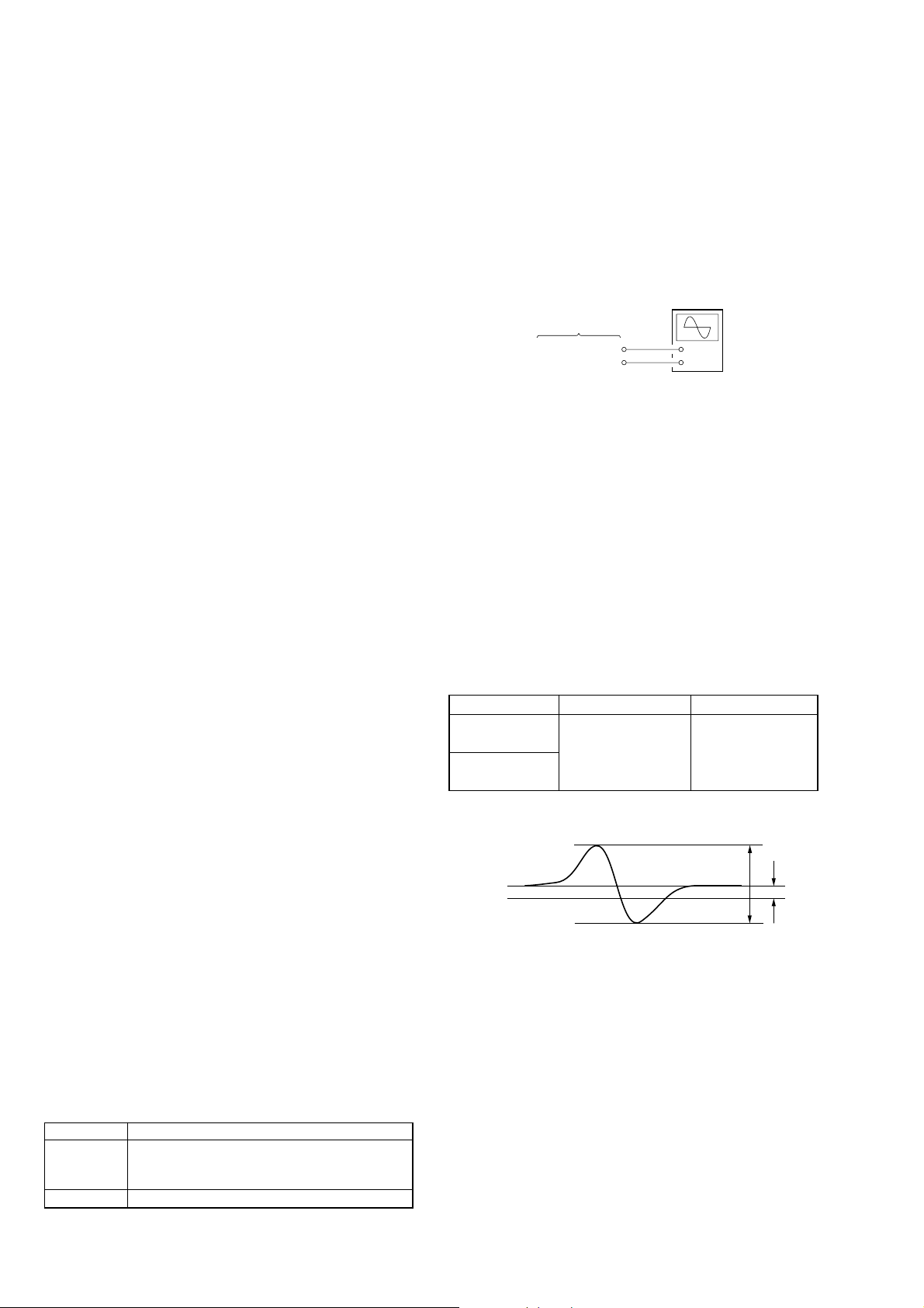
S curve waveform
VC
Note: For easier observation of this waveform, extend the sweep time
and raise the brightness.
0.7 to 1.7 Vp-p –0.1 to +0.1V
A
B
Checking and Connecting Location : See page 25.
Error List
Display Description
Toc Error * Error during the time from auto adjustment to TOC
Toc Error **** Illegal SACD (Such as a pirated version)
reading, Different type of disc (Such as a DVD disc),
Disc is dirty
24
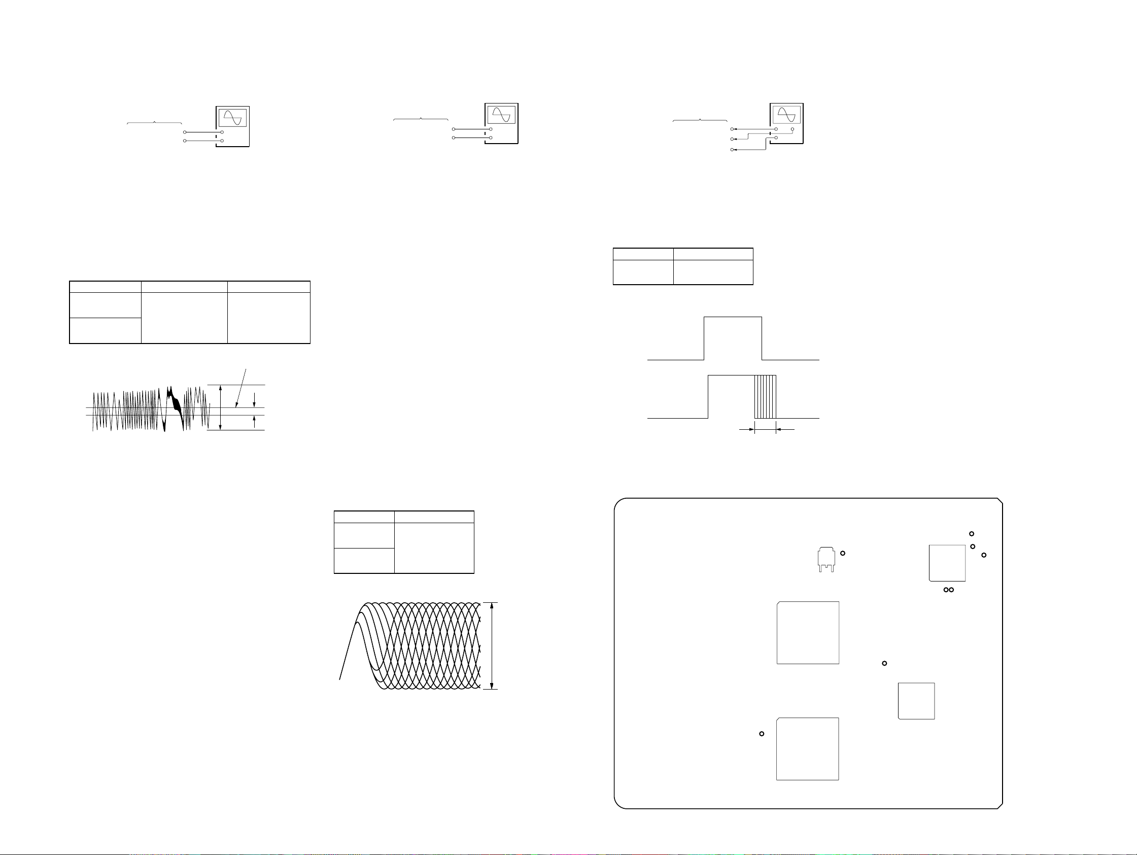
SCD-XA9000ES
A
CLV jitter waveform
e
V
Ver 1.1
Traverse Check
Connection:
oscilloscope
MAIN board
TP513 (TE)
TP504 (AVC)
+
–
Checking Method:
1. Under the condition of S curve waveform check mode in step
5, press the
lL
[ AMS ] dial.
2. After “W AIT” is displayed, the traverse wa veform check mode
will become active and “TRV MODE ON” will be displayed.
3. Connect an oscilloscope to the TP513 (TE) and TP504 (AVC)
on the MAIN board.
4. Check that the level A and B of waveform on the oscilloscope satisfy the specification.
Specified V alue:
Disc AB
SATD-S5 or
SATD-S4
PATD-012 or
YEDS-18
Traverse waveform
VC
0.9 to 1.4 Vp-p –0.1 to +0.1V
Center fo the waveform
A
B
Checking and Connecting Location : MAIN Board
RF Level Check
Connection:
oscilloscope
MAIN board
TP703 (RFAC)
TP704 (AGND)
+
–
Checking Method:
1. Under the condition of traverse waveform check mode in step
4, press the
lL
[ AMS ] dial.
2. Connect an oscilloscope to the TP703 (RFAC) and TP704
(AGND) on the MAIN board.
3. After “W AIT” is displayed, the RF waveform check mode will
become active and “PLAY 5th TRACK” (for the SA CD, “RF
MODE ON”) will be displayed, and the 5th music on the disc
will be played.
4. Check that the RF waveform is clear and the level satisfies the
specification.
5. Press the
lL
[ AMS ] dial (for the SACD, “RF JITTER
(5th)” will be displayed, and further press the AMS dial), and
“OUTSIDE TRACK” will be displayed and the outward track
of the disc will be played.
6. Check that the RF waveform is clear and the level satisfies the
specification.
7. Press the
[ AMS ] dial, and “INSIDE TRACK” will be
lL
displayed and the inward track of the disc will be played.
8. Check that the RF waveform is clear and the level satisfies the
specification.
9. After checking, press the
lL
[ AMS ] dial, and the test is
over when “BU MEASURE” is displayed.
10. Press the
[OPEN/CLOSE ] button to open the tray, and re-
A
move the test disc.
11. Using each type of disc, repeat from step 1 of S curve waveform check up to step 10 of RF level check.
12. When the check is over, press the
[POWER] button to turn the
power off.
Note: Take care not to leave the test disc in the set.
Specified Value:
Disc A
SATD-S5 or
SATD-S4
PATD-012 or
YEDS-18
RF signal waveform
0.9 to 1.4 Vp-p
VOLT/DIV: 200 m
TIME/DIV: 500 ns
CLV Jitter Check (CD only)
Connection:
oscilloscop
MAIN board
TP516 (RFCK)
TP517(WFCK)
TP808 (DGND)
(CH1)
(CH2)
+
+
–
Checking Method:
Under the condition of RF level check mode in step 3, connect the
oscilloscope to the TP516 (RFCK) (CH1), TP517 (WFCK) (CH2),
and the TP808 (DGND) (GND) on the MAIN board to check that
the value A of the waveform satisfies the specification.
Note: Take care not to leave the test disc in the set.
Specified Value:
Disc A
PATD-012 or
YEDS-18
35 µsec or less
Checking and Connecting Location:
– MAIN Board (Component Side) –
IC504
(RFAC)
4-7. i.LINK SIGNAL OPERATION CHECK
Connect the set to a unit equipped with the i.LINK terminal to
check if the bus reset occurs correctly. By this operation, a loose
connection of the connector or a disconnection of the i.LINK cable
can be checked.
Note: Do not perform the operation other than the specified operation in
the following i.LINK test mode, as the set otherwise may not operate normally.
Checking Method:
1. Press the
lL
[ AMS ] dial to select the “i.LINK” function (i.LINK
LED (blue) lights up). Then, with the
kept pressed, press the
and
[POWER] button to turn the power on, and rotate the
[TIME/TEXT] button
[OPEN/CLOSE ] button, [ ] button,
N
[ ] button in this order, so that the i.LINK test mode is
A
activated and “<< [B A CK] >>” is displayed on the fluorescent
display tube.
2. With “<< [BACK] >>” displayed on the fluorescent display
tube, rotate the
lL
[ AMS ] dial clockwise to advance the
display by five steps, so that “B.Rst. [000]” is displayed. T his
counter increments by one or several counts each time the bus
reset occurs.
3. Turn on the power of the unit equipped with the i.LINK terminal, and connect the set to the unit equipped with the i.LINK
terminal using the i.LINK cable to check if the bus reset occurs correctly. If the bus reset does not occur, or if the bus
reset occurs continuously, the i.LINK cable will be disconnected or the connector connection will be loose.
Note: The bus reset may not occur unless the power of the unit equipped
with the i.LINK terminal is turned on when it is connected.
4. With the set connected to the unit equipped with the i.LINK
terminal using the i.LINK cable, move the i.LINK cable to
check if the bus reset occurs. If the bus reset occurs though the
i.LINK cable is not removed, the i.LINK cable will be disconnected or the connector connection will be loose.
5. Press the
lL
[ AMS ] dial counterclockwise so as to display “<<
[BACK] >>”, and then press the
[POWER] button to turn the po wer off, or r otate the
[MENU] button, so that the
i.LINK test mode is deactivated.
TP513
(TE)
TP506
TP703
IC509
TP517
(WFCK)
(FE)
TP504
(AVC)
TP516
(RFCK)
x
IC701
A
Note: Clear RF waveform refers to the wav eform where ◊ shapes should
be distinctively observed in the center.
TP808
(DGND)
TP704
(AGND)
IC802
Checking and Connecting Location : MAIN Board
IC801
2525
SCD-XA9000ES
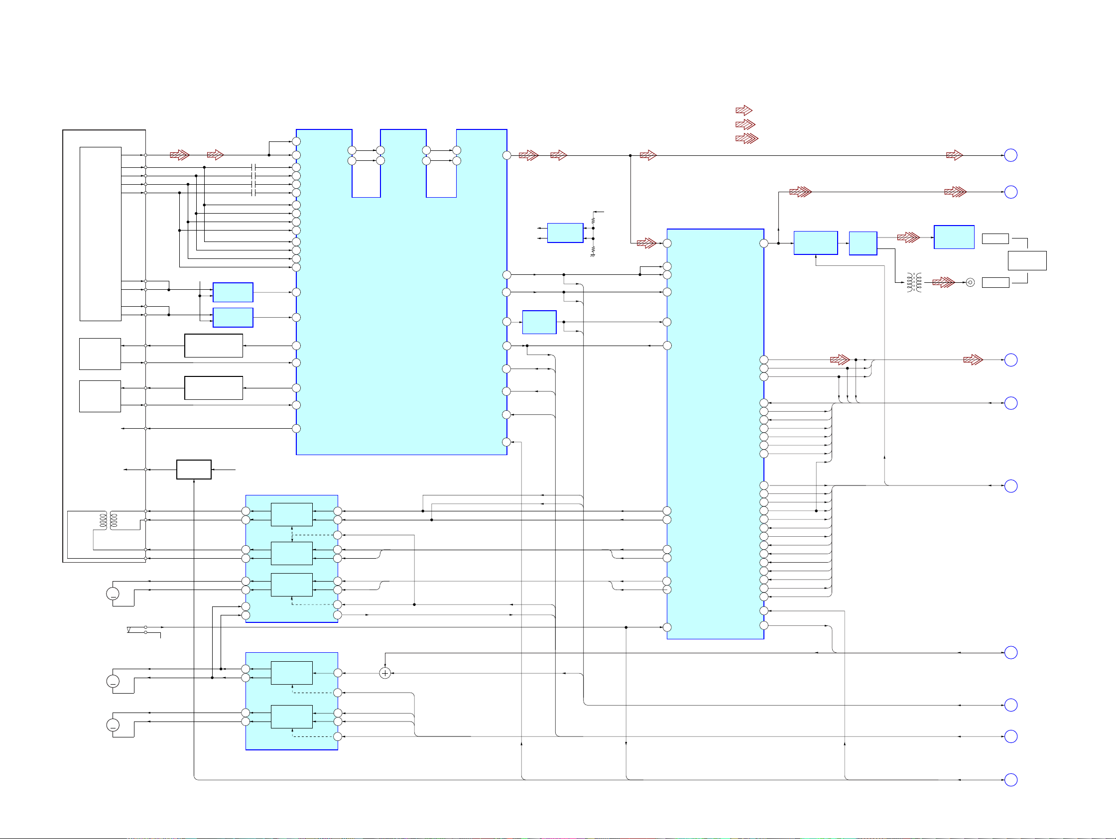
5-1. BLOCK DIAGRAM – RF/SERVO Section –
OPTICAL PICK-UP
BLOCK
(KHM-230AAA)
DETECTOR
LASER
DIODE
(SACD)
LASER
DIODE
(CD)
VC
(+2.5V)
MODULE
CIRCUIT B+
2-AXIS
DEVICE
(TRACKING)
M2
M
(SLED)
S1
(LIMIT)
M3
(SPINDLE)
(LOADING)
M
M1
M
DVD_LD
DVD_PD
CD_LD
CD_PD
VMOD
(FOCUS)
SECTION 5
DIAGRAMS
• Signal Path
: SACD PLAY
: CD PLAY (ANALOG OUT)
63
RF
A
B
C
D
E
F
G
H
D+3.3V
VC
COMPARATOR
IC081 (1/2)
COMPARATOR
IC081 (2/2)
AUTOMATIC POWER
CONTROL (FOR SACD)
Q001
AUTOMATIC POWER
CONTROL (FOR CD)
Q003
B+ SWITCH
Q002, 005
FD+
FD–
TD+
TD–
SD+
SD–
LOAD+
LOAD–
A+5V
FOCUS/TRACKING COIL DRIVE,
SLED MOTOR DRIVE
12
11
14
13
17
18
27
26
SPINDLE/LOADING
8
9
6
5
1
3
4
5
6
12
11
10
9
16
15
14
13
18
17
21
23
22
24
20
IC502
FOCUS
COIL
DRIVE
STANDBY1
TRACKING
COIL
DRIVE
SLED
MOTOR
DRIVE
STANDBY2
MOTOR DRIVE
IC512
SPINDLE
MOTOR
DRIVE
LOADING
MOTOR
DRIVE
RFSIN
DVDRFP
CD_A
CD_B
CD_C
CD_D
CD_E
CD_F
DVDLD
DVDPD
CDLD
CDPD
VC
A2
B2
C2
D2
A
B
C
D
MUTE2
MUTE1
ATOP
62
ATON
61
FOCUS/TRACKING ERROR AMP
FFDR
5
FRDR
6
9
TFDR
2
TRDR
3
SFDR
24
SRDR
23
20
25
17
13
22
21
2
60 53
59
SACD/CD RF AMP,
MUTE_LOAD
AIN
AIP
IC001
SP_ON
LOAD_IN
LOAD_OUT
FNP
FNN
54
DIP
RFAC
MIRR
SDATA
SCLK
LDON
SDEN
57
A+3.3V
+1.65V
+1.65V
39
TE
40
FE
38
PI
27
DATA_RF
47
CLK_RF
46
LDON
26
48
AVC
PI ERROR
AMP
IC004 (2/2)
MIRR
MUTE_2D
SP_ERR
VC BUFFER
IC004 (1/2)
FJMP1
FJMP2
SPDA
TE
FE
PI
TFDR
TRDR
SFDR
SRDR
DIGITAL SERVO PROCESSOR,
DIGITAL SIGNAL PROCESSOR,
DIGITAL FILTER
IC509
50
RFAC
40
SE
41
TE
39
FE
43
RFDC
20
MIRR
33
FFDR
34
FRDR
31
TFDR
32
TRDR
29
SFDR
30
SRDR
26
SSTP
52
55
DIN
: CD PLAY (DIGITAL OUT)
DOUT
PCMD
BCK
LRCK
XTAI
WDCK
EXCK
SBSO
WFCK
C2PO
DFCT
LOCK
FOK
COUT
SCOR
GFS
SCLK
SENS
CLOK
XLAT
DATA
MUTE
SQCK
SQSO
MD2
XRST
MDP
64
66
67
65
71
17
80
79
10
14
21
24
22
19
15
13
8
7
6
5
4
3
77
76
63
2
25
ON/OFF SWITCH
MDAT
BCLK
LRCK
768_CD
GSCOR
EXCK
SBSO
WFCK
C2PO
DFCT
LOCK
FOK
COUT
SCOR
GFS
SCLK
SENS
CLOK
XLAT
DATA
MUTE_CD
SQCK
SQSO
MD2
MDP
SPIN
DIGITAL OUT
IC810
WAVE
SHAPER
IC441
DOON
OPTICAL
TRANSCEIVER
IC442
T441
FJMP1, FJMP2, SPDA
MIRR, DATA_RF, CLK_RF, LDON,
SP_ON, LOAD IN, LOAD OUT,
MUTE LOAD, MUTE_2D, SP_ERR
RFAC
DOUT
OPTICAL
COAXIAL
MDP, SPIN
TE, FE, PI,
J391
A
(Page 27)
X
(Page 31)
DIGITAL (CD)
V
(Page 29)
B
(Page 27)
C
(Page 28)
E
(Page 27)
F
(Page 28)
G
(Page 28)
OUT
VMOD
SDEN
LIM_SW
XRST_CD
VMOD, SDEN,
LIM SW, XRST_CD
H
(Page 28)
2626
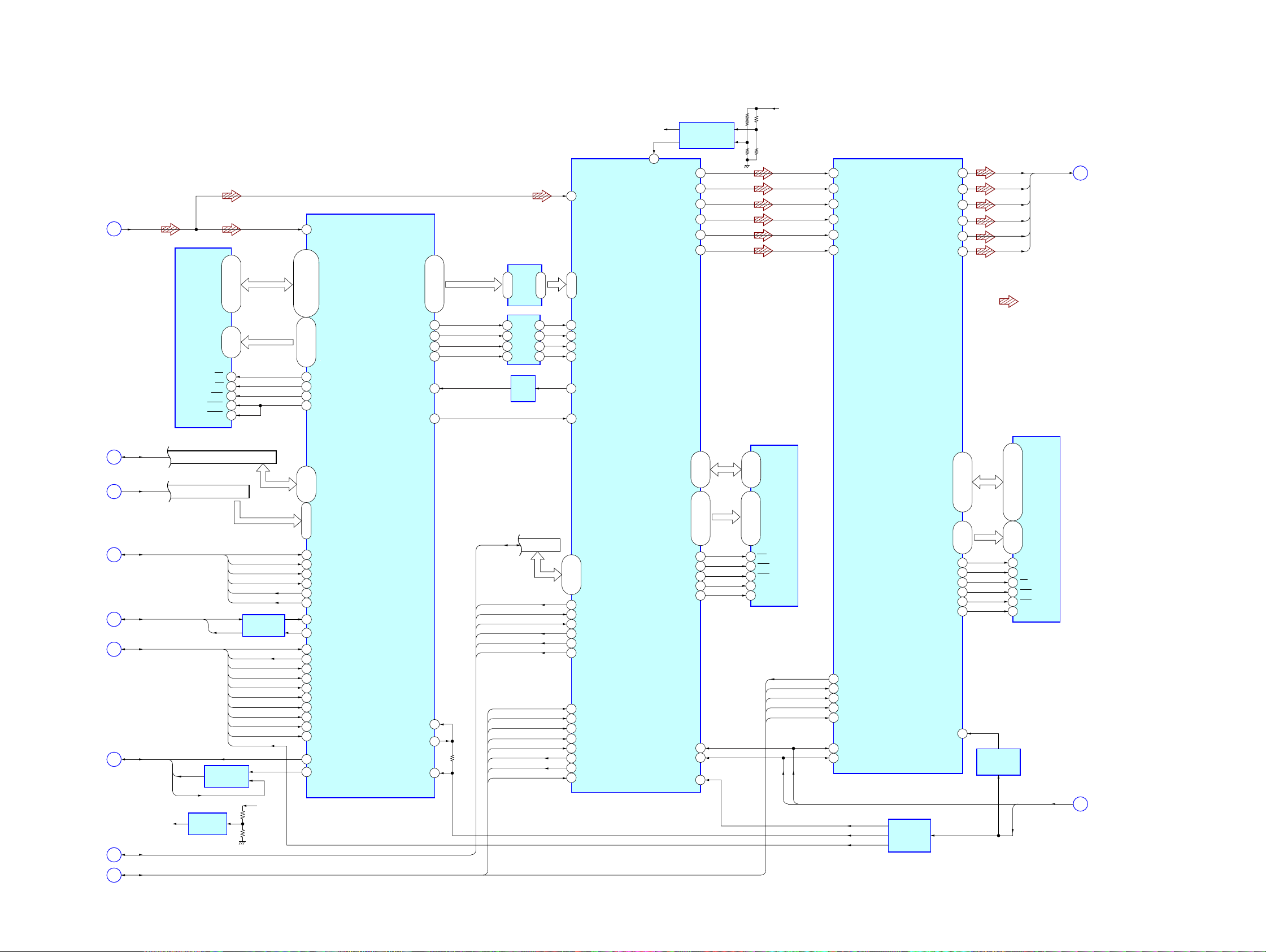
5-2. BLOCK DIAGRAM – MAIN Section (1/2) –
(Page 26)
RFAC
A
117
RFIN
SCD-XA9000ES
D+5V
127
WAVRB
CENTER VOLTAGE
GENERATOR
IC503
64
DSAL
66
DSAR
69
DSAC
71
DSASW
74
DSALS
76
DSARS
83
DLI
84
DRI
85
DCI
86
DLFEI
DLSI
87
DRSI
88
DLO
DRO
DCO
DLFEO
DLSO
DRSO
38
37
35
34
32
31
SDATAL
SDATAR
SDATAC
SDATASW
SDATALS
SDATARS
N
(Page 29)
DRVC +2.5V
126
WARFI
(Page 28)
(Page 28)
(Page 28)
(Page 26)
(Page 26)
(Page 28)
(Page 31)
LEVEL
SHIFT
9 – 2
11 – 18
169 – 176
166
SDCK
165
XSHD
167
XSAK
168
SDEF
164
XSRQ
WCK
123
82, 84, 85
78, 79, 81,
87
IANCO
88
IFULL
89
IEMPTY
91
IFRM
92
IOUTE
93
IBCK
9
XRST
10
SMUTE
2
XMSLAT
3
MSCK
MSDATI
4
MSDATO
6
7
MSREADY
115
TEST1
SD0 – 7
IOUT0 – IOUT5
DSD DECODER
IC801
XWE
XCAS
XRAS
DCLK
DCKE
PHREFI
BCKAI
MCKI
DQ0 – 7
139 – 136
134 – 131
A0 – 11
152,151,149,148
162–159,157–154
143
144
145
141
142
61
59
768FS
11
16Mbit D-RAM
IC808
DQ0 – 7
2 ,3 ,5 ,6
8 ,9 ,11 ,12
A0 – 11
20 , 19
21 – 24,27 – 32
15
WE
16
CAS
17
RAS
35
CLK
34
CKE
SIN_DY
SOUT_DSD
SCK_DSD
XCS_DY
RST_DY
128FS
64FS
DSD
DIGITAL
SIGNAL
PROCESSOR
IC802
D0 – D15
A0 – A11
CLK
CKE
CS
RAS
CAS
WE
75
SO
74
SI
SCLK
72
XCS
73
70
XRST
CLK512
80
PHRI
81
BCKAI
768FS
768_DVD
768_CD
CLOCK
GENERATOR
IC811
IOUT5
ANCIO
IFULL
IEMPTY
IFRM
IOUTE
IBCK
XRST_DSD
MUTE_DSD
XLAT_DSD
SCK_DSD
SOUT_DSD
SIN_DSD
RDY_DSD
SAMBA_TEST
IC812
5 15
LEVEL
4
SHIFT
3
IC813
2
LEVEL
SHIFT
IC814
DATA BUS
16
17
18
104 – 106
I/O0 – I/O15A0 – A9
2 – 5, 7 – 10,
16Mbit
D-RAM
IC706
D0 – D7
I
A0 – A7
J
DATA BUS
ADDRESS BUS
K
E
B
DVC
GFS_V
JIT
APDO
VC BUFFER
IC703 (2/2)
L
41 – 44, 46 – 49
27 – 32
21 – 24,
17
WE
33
OE
18
RAS
34
UCAS
LCAS
35
XRST_DVD
XHRD
XHWR
XCS1882
XINIT0
XINIT1
MDP
SPIN
GSCOR
EXCK
SBSO
WFCK
C2PO
BCLK
MDAT
LRCK
DFCT
SCOR
768_CD
COMPARATOR
IC703 (1/2)
LEVEL SHIFT
IC708
A+3.3V
MDB0 – MDBF
66 – 69, 71, 73 – 75,
96, 97, 99, 101, 102,
79 – 80,
MA0 – MA9
82 – 87, 89, 91
76
XMWR
94
XMOE
78
XRAS
95
XCAS
1, 2, 4
D0 – D7
172 – 176,
A0 – A7
5, 7, 9 – 14
164
XRST
17
XRD
18
XWR
XCS
19
XINT0
20
XINT1
21
MDIN2
137
SPO
135
GSCOR
146
EXCK
147
SBIN
148
151
WFCK
155
C2PO
158
BCLK
160
MDAT
LRCK
163
DFCT
145
SCOR
150
GFS
107
APEO
109
SACD DECODER
IC701
HDB0 – HDB7
XHWR
XHRD
XDRQ
HDB8
XHAC
MA11
XTAL
XTL2
XTL1
32, 30, 27, 24
44, 41, 39, 35,
48
49
46
26
53
93
167
169
170
IOUT0 –
• Signal Path
97, 98, 100
1 – 5, 7, 8, 90 – 95,
24 – 29
17 – 22,
14
15
13
12
11
10
68
CLOCK
GENERATOR
IC804
: SACD PLAY
16Mbit SD-RAM
IC803
DQ0 – DQ15
40, 42, 43, 45, 46, 48, 49
2, 3, 5, 6, 8, 9, 11, 12, 39,
27 – 32
19 – 24,
A0 – A11
35
CLK
34
CKE
18
CS
17
RAS
16
CAS
15
WE
256FS
(Page 29)
W
Y
(Page 28)
M
2727
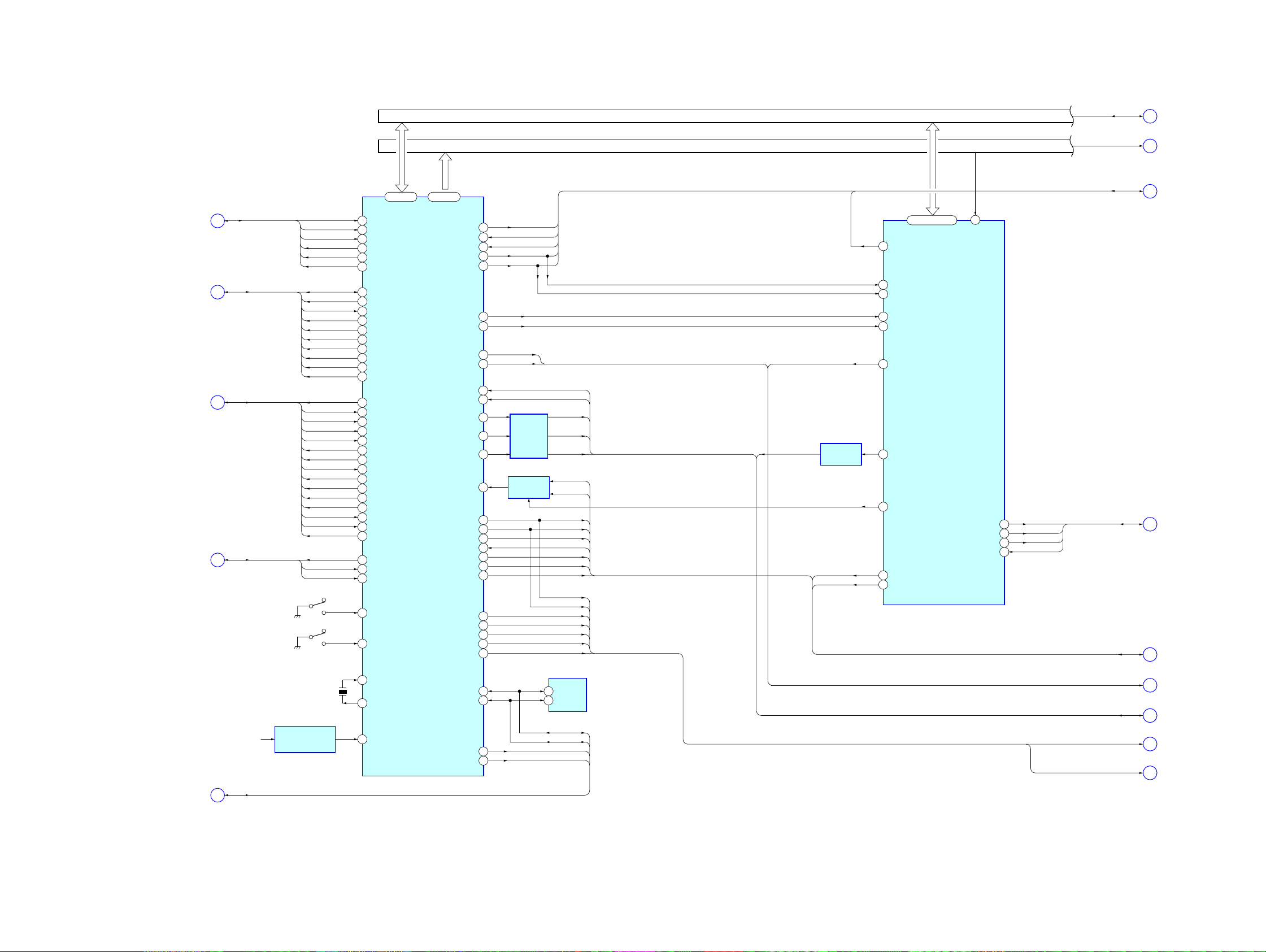
SCD-XA9000ES
5-3. BLOCK DIAGRAM – MAIN Section (2/2) –
F
(Page 26)
G
(Page 26)
C
(Page 26)
L
(Page 27)
Z
(Page 31)
S001
(LOADING IN)
S002
(LOADING OUT)
D+3.3V
MLS_SIO, MLS_SCK,
MLS_RST, MLS_OSC
SIGNAL GENERATOR
OFF
OFF
OUT
DATA BUS
ADDRESS BUS
89 – 9614 – 21
CPU
IC901
A0 – A7D0 – D7
XCS_DVD
INIT0_DVD
INIT1_DVD
XCS_IO
XDIS_IO
SWGUP
AMUT_MCH
BUSY_DP
SIN_DP
SOUT_DP
SCK_DP
REQ-DP
SIN_DSD
SOUT_DSD
SCK_DSD
XLAT_DSD
RDY_DSD
MUTE_DSD
XCS_DY
RST_DY
INIT_DF
LATCH_DF
LATCH_DF_B
MODE_SACD
EEPSIO
EEPSCL
MLS_RST
MLS_OSC
XRD
XWR
MULTI
12
22
23
85
84
11
10
99
60
51
52
53
54
56
48
49
50
47
27
28
57
2
97
98
62
5
76
78
79
61
82
XCS1882
XINIT0
XINIT1
XHRD
XHWR
SWGUP
AMUT_MCH
LEVEL
SHIFT
IC906 (1/2)
DATA SELECT
IC902
XFBSY
XIFCS
SIN_DSD
SIN_DY
SOUT_DSD
SCK_DSD
XLAT_DSD
RDY_DSD
MUTE_DSD
XCS_DY
RST_DY
DATA_DF
CLK_DF
INIT_DF
LAT_DF_A
LAT_DF_B
MODE_SACD
MULTI
EEPROM
IC903
SDA
5
SCL
6
MLS_SIO
MLS_SCK
MLS_RST
MLS_OSC
SIO
SOO
SCO
AMUTE
XFRRST
LEVEL SHIFT
IC906 (2/2)
XRST_DSD
SAMBA_TEST
TE
FE
PI
FJMP1
FJMP2
SPDA
DATA_RF
CLK_RF
MIRR
LDON
MUTE_2D
SP_ERR
SP_ON
MUTE_LOAD
LOAD_IN
LOAD_OUT
MD2
SENS
LOCK
FOK
GFS
DATA
XLAT
COUT
SCLK
CLOK
MUTE_CD
SQCK
SQSO
SCOR
DOON
r
IN
r
X901
20MHz
RESET
IC905
APDO
GFS_V
65
TE
67
FE
66
PI
7
FCS_JMP_1
8
FCS_JMP_2
43
SPDA
DATA_RF
83
77
CLK_RF
MIRR_RF
25
LDON
100
MUTE_2D
4
SP_ERR
59
6
SP_ON
1
MUTE_LOAD
45
LOAD_IN
LOAD_OUT
46
DOCTRL
3
SENS_CD
9
75
LOCK_CD
74
FOK_CD
71
GFS_CD
34
DATA_CD
XLAT_CD
36
29
COUT_CD
SCLK_CD
72
CLOK_CD
35
73
MUTE_CD
37
SQCK_CD
SQSO
33
SCOR_CD
26
DOON
63
44
APDO
JIT
JITTER
64
58
GFS_DVD
30
IN_SW
31
OUT_SW
40
XTAL
41
EXTAL
RST
38
DATA BUS
ADDRESS BUS
XRST_DVD
RST_DVD
31
11
XWR
XRD
10
XCS
9
RST
24
37
AMUTE
26
RST_DP
1
SI_SELRKSW
25
RST_DSD
36
ISBTEST
12 – 16, 19 – 22
I/O EXPANDER
IC904
22
AD0 – D7
VMOD
RST_CD
SDEN
LIM_SW
XHRD, XHWR, XCS1882,
XINIT0, XINIT1, XRST_DVD
33
32
35
44
VMOD
XRST_CD
SDEN
LIM_SW
SIN_DSD, SIN_DY, SOUT_DSD,
SCK_DSD, XLAT_DSD, RDY_DSD,
MUTE_DSD, XCS_DY, RST_DY,
XRST_DSD, SAMBA_TEST
DATA_DF, CLK_DF, INIT_DF,
DATA_DF, CLK_DF, INIT_DF,
LAT_DF_A, LAT_DF_B, MULTI
D0 – D7
A0 – A7
SWGUP, AMUTE,
AMUT_MCH
XFBSY, SIO, SOO,
SCO, XIFCS, XFRRST
LAT_DF_A, LAT_DF_B,
MODE_SACD, MULTI
I
J
K
H
M
O
Q
P
S
(Page 27)
(Page 27)
(Page 27)
(Page 26)
(Page 27)
(Page 30)
(Page 32)
(Page 29)
(Page 30)
2828
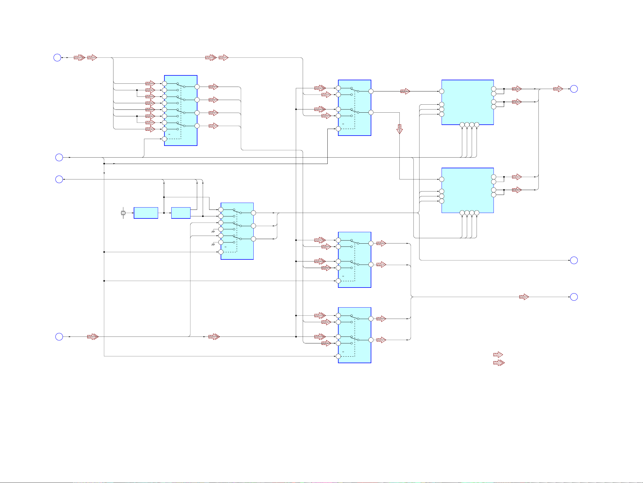
5-4. BLOCK DIAGRAM – AUDIO Section (1/2) –
(Page 27)
N
4A
14
4B
13
3A
11
3B
10
1A
2
1B
3
2A
5
2B
6
A/B
1
(Page 28)
DATA_DF, CLK_DF, INIT_DF,
LAT_DF_A, LAT_DF_B,
MODE_SACD, MULTI
P
SDATAL
SDATALS
SDATAC
SDATAR
SDATAS
SDATASW
MULTI
DATA SELECTOR
IC305
SCD-XA9000ES
DIGITAL FILTER,
CURRENT PULSE,
5DATA
LRCK
4
BCK
6
SCKI
7
D/A CONVERTER
IC101
MDI13MC14CS1RST
12
CLK_DF
LAT_DF_B
DATA_DF
INT_DF
25LOUTL+
16LOUTR+
26LOUTL–
17LOUTR–
FL–
FL+
R
(Page 30)
DATA SELECTOR
IC307
SW
SL
C
SR
SDATAL
SDATAR
4A
14
4B
13
1A
2
1B
3
A/B
1
4Y
12
LRCK/G
1Y
4
BCK/G
SCKI
4Y
12
3Y
9
1Y
4
2Y
7
(Page 27)
(Page 26)
W
V
256FS,
128FS, 64FS
LRCK, BCLK,
MDAT
MODE_SACD
11.2896MHz
X301
CLOCK BUFFER
IC302
256FS
COUNTER
IC303
128FS
LRCK
BCLK
MDAT
64FS
2
3
5
6
11
10
1
SWITCHING
IC304
1A
1B
2A
2B
3A
3B
A/B
7
INT_DF
25LOUTL+
16LOUTR+
7
7
26LOUTL–
17LOUTR–
7
DIGITAL FILTER,
CURRENT PULSE,
D/A CONVERTER
IC201
• Signal Path
: SACD PLAY
5DATA
LRCK/G
BCK/G
SCKI
1Y
2Y
3Y
SCKI
4
LRCK/G
7
BCK/G
9
SL
SR
C
SW
DATA SELECTOR
4A
14
4B
13
1A
2
1B
3
A/B
1
DATA SELECTOR
4A
14
4B
13
1A
2
1B
3
A/B
1
IC308
IC306
4Y
12
1Y
4
4Y
12
1Y
4
CDTL/SDTSL
CDTR/SDTSR
CDTL/SDTC
CDTR/SDTSW
LRCK
4
BCK
6
SCKI
7
MDI13MC14CS1RST
12
DATA_DF
CLK_DF
LAT_DF_A
FR–
FR+
SCKI, LRCK/G, BCK/G
CDTL/SDTSL, CDTR/SDTSR,
CDTL/SDTC, CDTR/SDTSW
T
U
(Page 30)
(Page 30)
: CD PLAY (ANALOG OUT)
2929
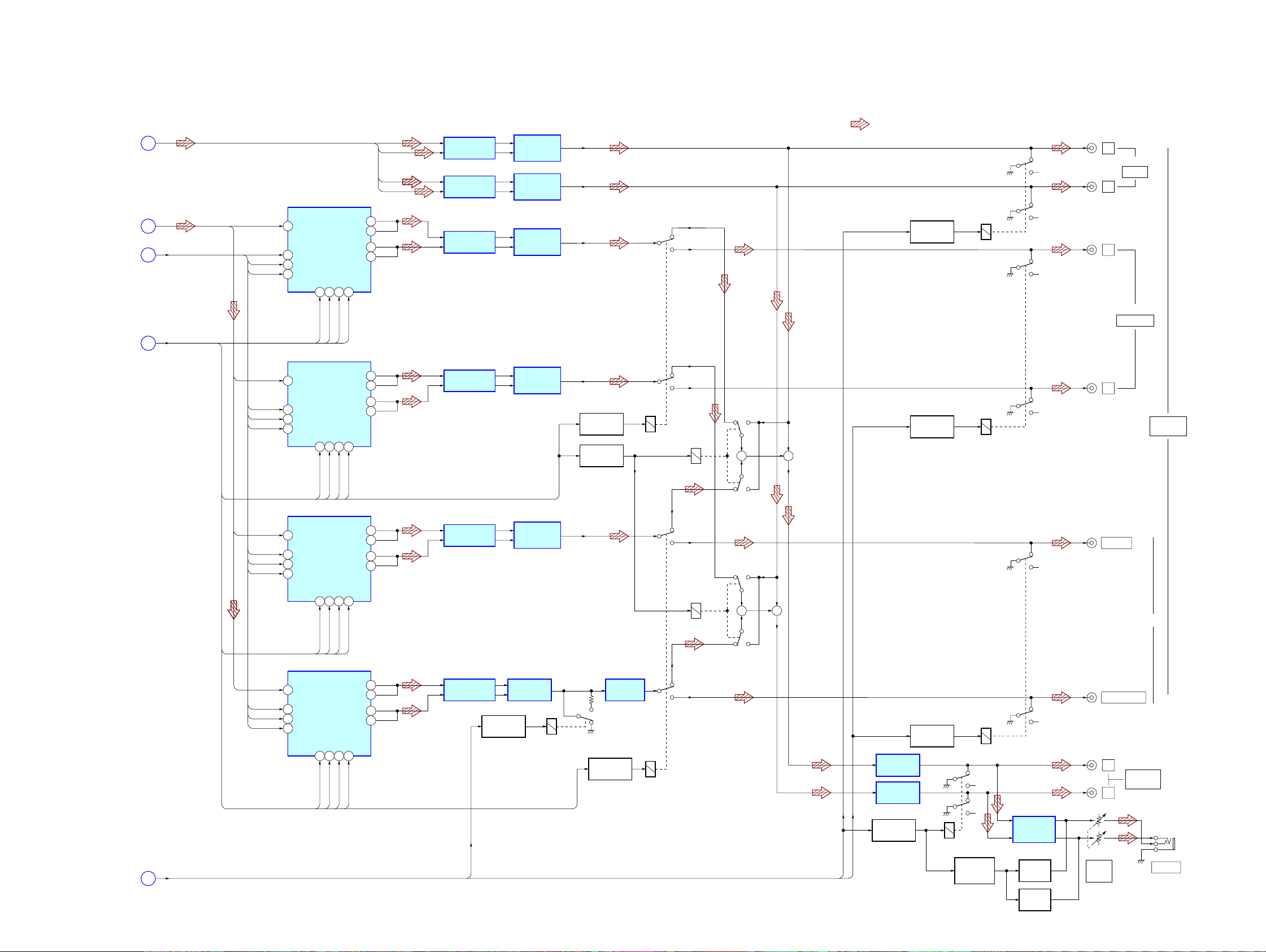
SCD-XA9000ES
5-5. BLOCK DIAGRAM – AUDIO Section (2/2) –
R
(Page 29)
U
(Page 29)
SCKI, LRCK/G, BCK/G
T
(Page 29)
DATA_DF, CLK_DF,
LAT_DF_A, LAT_DF_B,
INIT_DF, MULTI
S
(Page 28)
CDTL/
SDTSL
LRCK/G
BCK/G
SCKI
CDTL/
SDTSR
LRCK/G
BCK/G
SCKI
5 DATA
4
LRCK
6
BCK
7
SCKI
5 DATA
4
LRCK
6
BCK
7
SCKI
MDI13MC14CS1RST
12
DATA_DF
CLK_DF
LAT_DF_B
MDI13MC14CS1RST
12
INIT_DF
FL–
FL+
FR –
FR+
7
25LOUTL+
16LOUTR+
7
7
26LOUTL–
17LOUTR–
7
DIGITAL FILTER,
CURRENT PULSE,
D/A CONVERTER
25LOUTL+
7
16LOUTR+
7
26LOUTL–
7
17LOUTR–
7
DIGITAL FILTER,
CURRENT PULSE,
D/A CONVERTER
IC1101
IC1201
I-V CONVERTER
IC102
I-V CONVERTER
IC202
I-V CONVERTER
IC1102
I-V CONVERTER
IC1202
AUDIO FILTER,
LINE AMP
IC103
AUDIO FILTER,
LINE AMP
IC203
AUDIO FILTER,
LINE AMP
IC1103
AUDIO FILTER,
LINE AMP
IC1203
RELAY DRIVE
Q1151, 1152
RELAY DRIVE
Q394, 395
RY1151
RY353
+ +
• Signal Path
: SACD PLAY
RELAY DRIVE
Q153, 154
RELAY DRIVE
Q1153, 1154
RY152
RY1152
L
R
L
R
J301
FRONT
J1301
SURROUND
ANALOG
5.1CH OUT
CDTL/
SDTC
LRCK/G
BCK/G
SCKI
CDTR/
SDTSW
LRCK/G
BCK/G
SCKI
5 DATA
4
LRCK
6
BCK
7
SCKI
5 DATA
4
LRCK
6
BCK
7
SCKI
DATA_DF
CLK_DF
LAT_DF_A
MDI13MC14CS1RST
12
DATA_DF
CLK_DF
LAT_DF_B
MDI13MC14CS1RST
12
DATA_DF
CLK_DF
LAT_DF_A
INIT_DF
INIT_DF
INIT_DF
25LOUTL+
7
16LOUTR+
7
26LOUTL–
7
17LOUTR–
7
DIGITAL FILTER,
CURRENT PULSE,
D/A CONVERTER
25LOUTL+
7
16LOUTR+
7
26LOUTL–
7
17LOUTR–
7
DIGITAL FILTER,
CURRENT PULSE,
D/A CONVERTER
IC2101
IC2201
I-V CONVERTER
IC2102
I-V CONVERTER
IC2202
AUDIO FILTER
IC2203 (1/2)
RELAY DRIVE
Q2155, 2156
AUDIO FILTER,
LINE AMP
IC2103
RY2153
MULTI
MULTI
LINE AMP
IC2203 (2/2)
RELAY DRIVE
Q2151, 2152
RY2151
RY352
CENTER
+
+
J2301
SUB WOOFER
RY2152
L
J351
ANALOG
2CH OUT
R
LINE BUFFER
IC351
LINE BUFFER
IC352
RELAY DRIVE
Q2153, 2154
O
(Page 28)
SWGUP, AMUTE,
AMUT_MCH
SWGUP
HEADPHONE
AMP
IC371
MUTING
Q381
MUTING
Q371
RV601
PHONE
LEVEL
J601
PHONES
AMUT_MCH
AMUTE
RELAY DRIVE
Q391, 392
RY351
MUTING
CONTROL
Q393
3030
 Loading...