

Page 1
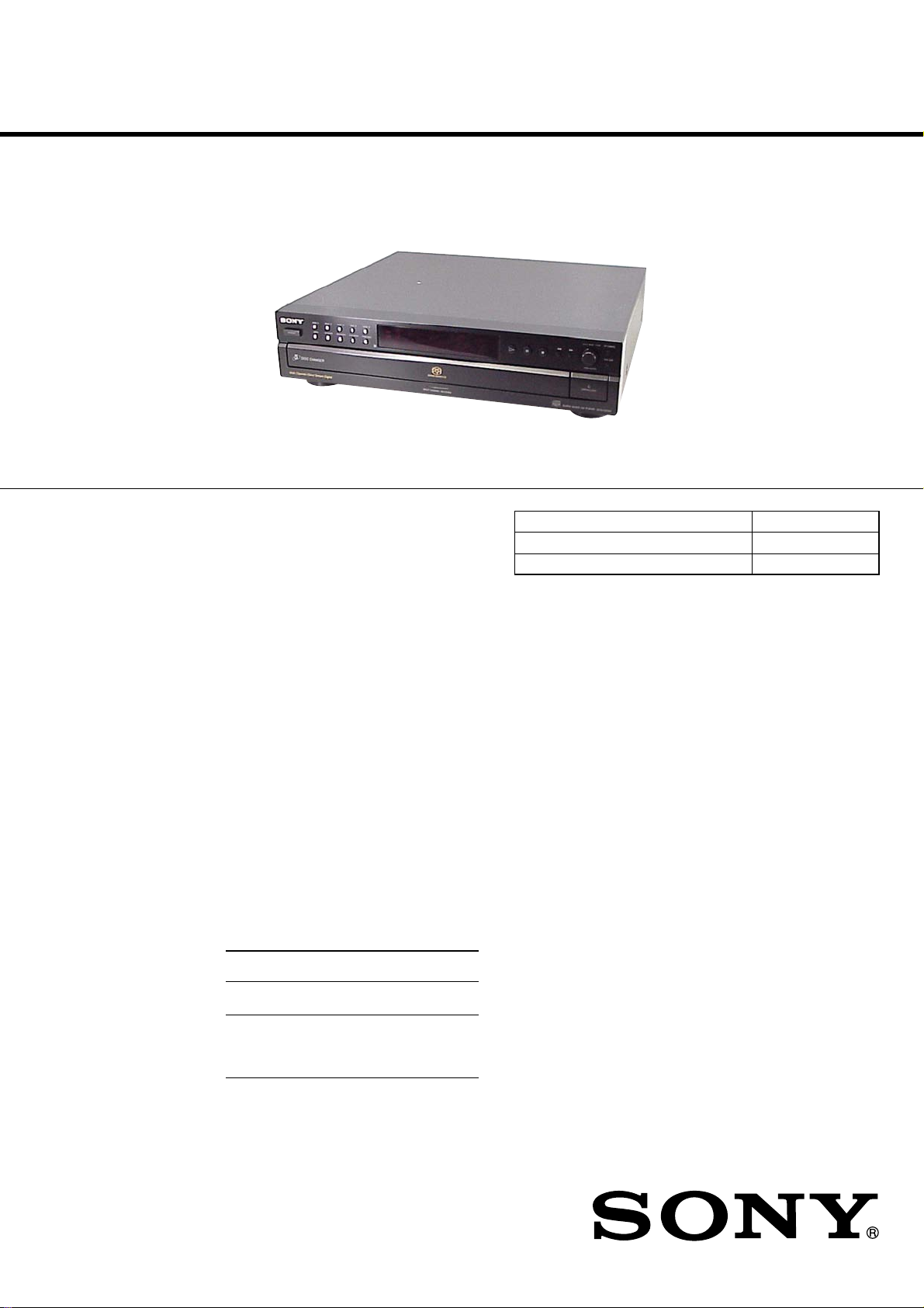
SCD-CE595
SERVICE MANUAL
Ver. 1.3 2006.08
SPECIFICATIONS
US Model
Canadian Model
AEP Model
UK Model
Model Name Using Similar Mechanism NEW
CD Mechanism Type CDM79C-DVBU51
Optical Pick-up Name DBU-3
When a Super Audio CD is played
Playing frequency range 2 Hz to 100 kHz
Frequency response 2 Hz to 40 kHz (–3 dB)
Dynamic range 100 dB or more
Total harmonic distort ion r at e
Wow and flutter Value of measurable limit
When a CD is played
Frequency response 2 Hz to 20 kHz
Dynamic range 96 dB or more
Total harmonic distort ion r at e
Wow and flutter Value of measurable limit
Output connector
Jack type Output
ANALOG
5.1CH OUT
DIGITAL
(CD) OUT
OPTICAL*
*Output only the audio signals of the CD
Phono
jacks
Square
optical
output
connector
0.0035 % or less
(±0.001 % W. PEAK) or
less
0.0039 % or less
(±0.001 % W. PEAK) or
less
level
2 Vrms (at
50 kilohms)
–18 dBm (Light
Load
impedance
Over 10
kilohms
emitting
wave length:
660 nm)
General
Laser Semiconductor laser
Power requirements
US, Canadian:
AEP, UK:
Power consumption 15 W
Dimensions (w/h/d) 430 110 420 mm incl.
Mass (approx.) 5.5 kg
Supplied accessories
Audio connecting cord Red and White 2 (1)
Remote commanderRM-SX800 (1)
Battery R6 (size-AA) (2)
Design and specifications are subject to change
without notice.
(Super Audio CD: λ = 650
nm) (CD: λ = 780 nm)
Emission duration:
continuous
1
20 V AC, 60 Hz
230 V AC, 50/60 Hz
××
projecting parts
×
9-879-006-04
2006H16-1
© 2006.08
SUPER AUDIO CD PLAYER
Sony Corporation
Home Audio Division
Published by Sony Techno Create Corporation
Page 2
SCD-CE595
TABLE OF CONTENTS
1. SERVICING NOTES ........................................... 3
2. GENERAL ............................................................ 4
3. TEST MODE......................................................... 6
4. DIAGRAMS
4-1. Block Diagram ................................................................ 8
4-2. Printed Wiring Board — RF Section — ......................... 9
4-3. Schematic Diagram — RF Section — ........................... 10
4-4. Printed Wiring Board — MAIN Section — ................... 11
4-5. Schematic Diagram — MAIN Section (1/4) — ............ 12
4-6. Schematic Diagram — MAIN Section (2/4) — ............ 13
4-7. Schematic Diagram — MAIN Section (3/4) — ............ 14
4-8. Schematic Diagram — MAIN Section (4/4) — ............ 15
4-9. Printed Wiring Board — DISPLAY Section — ............ 16
4-10. Schematic Diagram — DISPLAY Section — ................ 17
4-11. Printed Wiring Board — MD-94 Board Section — ...... 18
4-12. Schematic Diagram — MD-94 Board Section — .......... 19
5. EXPLODED VIEWS
5-1. Main Section.................................................................... 22
5-2. Front Panel Section ......................................................... 23
5-3. Chassis Section ................................................................ 24
5-4. CD Mechanism Section (1) (CDM79C-DVBU51) ......... 25
5-5. CD Mechanism Section (2) (CDM79C-DVBU51) ......... 26
NOTES ON HANDLING THE OPTICAL PICK-UP
BLOCK OR BASE UNIT
The laser diode in the optical pick-up block may suffer electrostatic
break-down because of the potential difference generated by the
charged electrostatic load, etc. on clothing and the human body.
During repair, pay attention to electrostatic break-down and also
use the procedure in the printed matter which is included in the
repair parts.
The flexible board is easily damaged and should be handled with
care.
NOTES ON LASER DIODE EMISSION CHECK
The laser beam on this model is concentrated so as to be focused on
the disc reflective surface by the objective lens in the optical pickup block. Therefore, when checking the laser diode emission,
observe from more than 30 cm away from the objective lens.
CAUTION
Use of controls or adjustments or performance of procedures
other than those specified herein may result in hazardous radiation
exposure.
This appliance is
classified as a CLASS 1
LASER product. This
label is located on the
rear exterior.
6. ELECTRICAL PARTS LIST ............................ 27
LASER DIODE AND FOCUS SEARCH OPERATION
CHECK
Carry out the “S curve check” in “CD section adjustment” and check
that the S curve waveform is output three times.
Notes on chip component replacement
• Never reuse a disconnected chip component.
• Notice that the minus side of a tantalum capacitor may be
damaged by heat.
Flexible Circuit Board Repairing
• Keep the temperature of the soldering iron around 270 °C
during repairing.
• Do not touch the soldering iron on the same conductor of the
circuit board (within 3 times).
• Be careful not to apply force on the conductor when soldering
or unsoldering.
SAFETY-RELATED COMPONENT WARNING!!
COMPONENTS IDENTIFIED BY MARK 0 OR DOTTED LINE
WITH MARK 0 ON THE SCHEMATIC DIAGRAMS AND IN
THE PARTS LIST ARE CRITICAL TO SAFE OPERATION.
REPLACE THESE COMPONENTS WITH SONY PARTS WHOSE
PART NUMBERS APPEAR AS SHOWN IN THIS MANUAL OR
IN SUPPLEMENTS PUBLISHED BY SONY.
2
ATTENTION AU COMPOSANT AYANT RAPPORT
À LA SÉCURITÉ!
LES COMPOSANTS IDENTIFIÉS PAR UNE MARQUE 0 SUR
LES DIAGRAMMES SCHÉMATIQUES ET LA LISTE DES
PIÈCES SONT CRITIQUES POUR LA SÉCURITÉ DE
FONCTIONNEMENT. NE REMPLACER CES COM- POSANTS
QUE PAR DES PIÈCES SONY DONT LES NUMÉROS SONT
DONNÉS DANS CE MANUEL OU DANS LES SUPPLÉMENTS
PUBLIÉS PAR SONY.
Page 3
SECTION 1
tapering driver
1
2
r
SERVICING NOTES
SCD-CE595
SAFETY CHECK-OUT
After correcting the original service problem, perform the following
safety check before releasing the set to the customer:
Check the antenna terminals, metal trim, “metallized” knobs, screws,
and all other exposed metal parts for AC leakage.
Check leakage as described below.
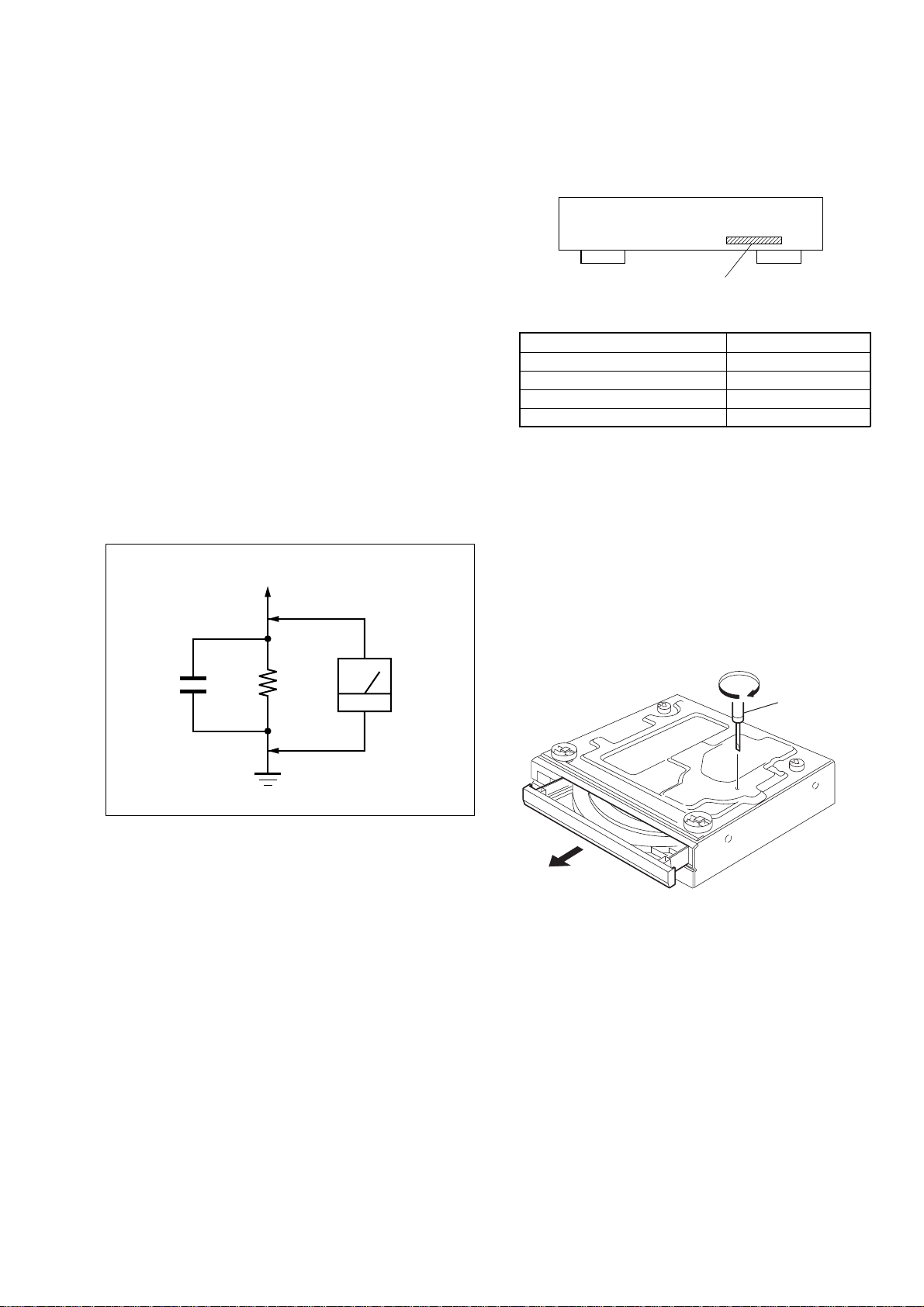
LEAKAGE TEST
The AC leakage from any exposed metal part to earth ground and
from all exposed metal parts to any exposed metal part having a
return to chassis, must not exceed 0.5 mA (500 microamperes.).
Leakage current can be measured by any one of three methods.
1. A commercial leakage tester, such as the Simpson 229 or RCA
WT -540A. Follow the manufactur ers’ instructions to use these
instruments.
2. A battery-operated A C milliammeter . The Data Precision 245
digital multimeter is suitable for this job.
3. Measuring the voltage drop across a resistor by means of a
VOM or battery-operated AC v oltmeter. The “limit” indication
is 0.75 V, so analog meters must hav e an accurate low-voltage
scale. The Simpson 250 and Sanwa SH-63Trd are examples
of a passive VOM that is suitable. Nearly all battery operated
digital multimeters that have a 2 V A C range are suitable. (See
Fig. A)
To Exposed Metal
Parts on Set
MODEL IDENTIFICATION
– Back Panel –
Parts No.
MODEL Part No.
US Model 4-255-250-0[ ]
Canadian Model 4-255-250-1[ ]
AEP Model 4-255-250-2[ ]
UK Model 4-255-250-3[ ]
HOW TO OPEN THE DISC TRAY WHEN POWER
SWITCH TURNS OFF
Insert a tapering driver into the aperture of the unit bottom, and turn
in the direction of arrow.
Use a flat (-) head screwdriver to open the disc tray by manual
operation. (Flat head screwdriver with nominal blade length of
3mm.)
* To close the disc table, turn the driver in the reverse direction.
AC
0.15 µF
1.5 k
Ω
Earth Ground
voltmete
(0.75 V)
Fig. A. Using an AC voltmeter to check AC leakage.
3
Page 4
SCD-CE595
q
q
q
q
q
q
q
q
q
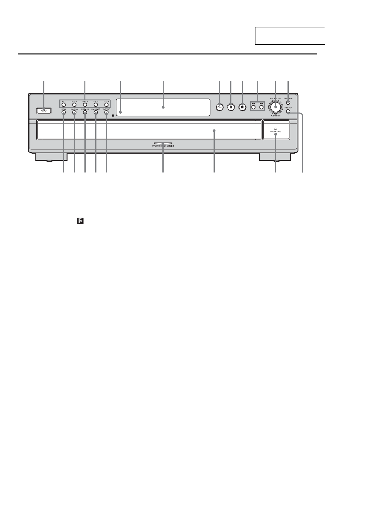
Front Panel
123 4 56789q;
SECTION 2
GENERAL
This section is extracted
from instruction manual.
g
h
j
k
l
A POWER switch (9)
B DISC 1-5 buttons (9, 14)
Press to select the disc directly.
C Remote sensor (6)
D Display window (10)
E H button (9, 13, 14)
F X button (9)
G x button (9, 15)
H m/M buttons (13)
I l AMS L dial
(AMS: Automatic Music Sensor) (8, 9, 10,
12, 13, 14, 16, 17, 19)
J EX-CHANGE button (12)
Press to replace discs while playing a disc.
K DISC SKIP button (9, 12, 14)
Press to select the disc.
L A OPEN/CLOSE button (9)
M Disc tray (9)
N MULTI CHANNEL DECODING indicator
Turns on when you turn on the player, or when the
Multi-channel Super Audio CD is loaded and
select the multi-channel playback area by pressing
MULTI/2CH.
f
O TIME/TEXT button (11)
Each time you press the button, the playing time of
the track, the remaining time of the disc, or TEXT
information appears in the display.
P PLAY MODE button (9, 14)
Press to select the play mo de.
Q MULTI/2CH button (5, 10)
Press to select the playback area when a disc with
the 2 channel area and the multi-channel area
(page 5) is loaded.
R SA-CD/CD button (5, 9)
Each time you press the button while playing back
a hybrid dis c, the layer to be played b ack switches
between the SA-CD layer and the CD layer.
S MENU button (8, 9, 10, 12, 16, 17, 19)
Press to enter the menu.
Press to exit from the menu and return to the
normal display.
d
s
a
4
Page 5
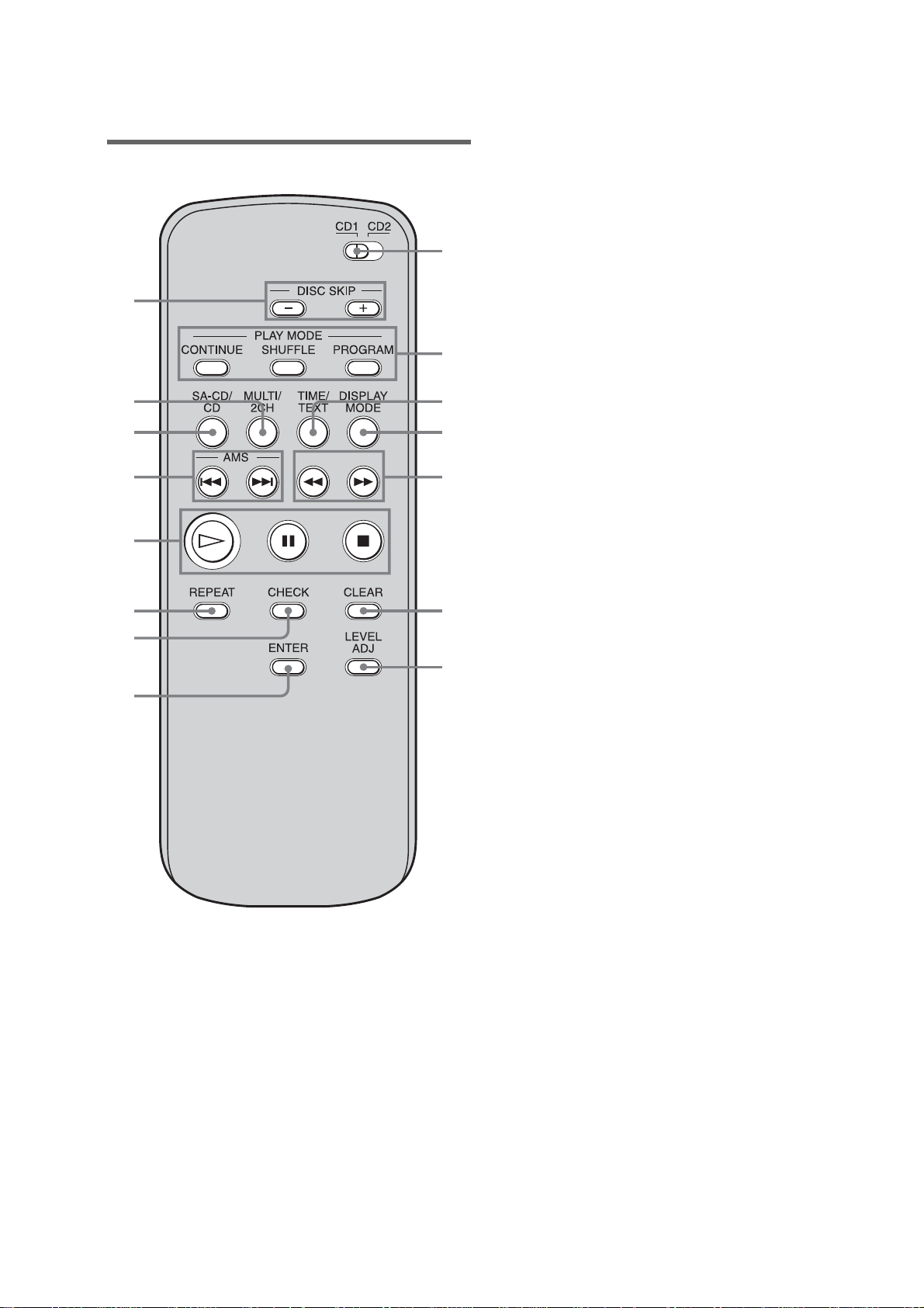
Remote
qg
qf
qd
qs
qa
q;
9
8
1
2
3
4
5
6
7
SCD-CE595
A CD1/2 (command mode) switch (8)
Select the command mo d e.
B CONTINUE button (9, 14)
Press to resume Continuous Play from Shuffle Play
or Program Play.
SHUFFLE button (14)
PROGRAM button (14)
C TIME/TEXT button (11)
Each time you press the button, the playing time of
the track, the remaining time of the disc, or TEXT
information appears in the display.
D DISPLAY MODE button (12)
Press to turn the display information off or on.
E m/M buttons (13)
F CLEAR button (14, 15)
Press to delete a progra me d tr a c k nu mber.
G LEVEL ADJ button (17)
Press to adjust the output level balanc e for the
Multi-channel management function (page 15).
H ENTER button (8, 10, 12, 14, 16, 18, 19)
I CHECK button (15)
Press to check the programed order.
J REPEAT button (13)
K H button (9, 13, 14)
X button (9)
x button (9, 15)
L AMS ./> buttons
(AMS: Automatic Music Sensor) (8, 9, 10,
12, 13, 14, 16, 18, 19)
M SA-CD/CD button (5, 9)
Each time you press the button while playing back
a hybrid disc, the layer to be played back switches
between the SA-CD layer and the CD layer.
N MULTI/2CH button (5, 10)
Press to select the playback area when a disc with
the 2 channel area and the multi-channel area
(page 5) is loaded.
O DISC SKIP +/– buttons (9, 12, 14)
Press to select the disc .
5
Page 6

SCD-CE595
SECTION 3
TEST MODE
1. Setting Methed of Test Mode
Press three buttons m , [PUSH ENTER] and [POWER] simulta-
neously, The test mode becomes active. Then all segments of the
fluorecent indicator tube are turned on.
2. FL Tube Grid, Segments Check
Procedure:
1. Grid of all segments lights up sequentially starting from 1G to
16G.
2. The vertical line (total 5 lines) of all grids lights up sequentially
in the range of 5G to 16 G starting from the left.
3. The horizontal line of (total 7 lines) of all grids lights up
sequentially in the range of 5G to 16G starting from the top.
3. Sircs Receive Check
Procedure:
1. The message “SIRCS CHECK” is displayed on the fluorecent
indicator tube.
2. With the machine in the status that is set in step 2, press any
on the remote commander. The machine enters the ke y check
standby state. (When the H key or the x key is pressed,
the reception check is canceled.)
4. Key Check
Procedure:
1. In the key check mode, the fluorecent indicator displays “KEY
CHECK**”. Each time a button is pressed, “**” value.
However, once a button is pressed, it is no longer taken into
account.
2. To exit from this mode, the message “JOG CHECK” is
displayed.
5. Jog Check
Procedure:
1. After the key check is completed, turn JOG clockwise to tur n
on the calendar segments sequentially . When the segment “15”
is confirmed, turn JOG counter-clockwise that turns off the
calendar segment. When the segment “1” is conf irmed, this is
the end of check.
6. Releasing Meted of Test Mode
1. After all the checks are completed, confirm to see that the
display “TEST-END” appears. The message indicates that
the check is ended normally.
2. Press the [POWER] button to turn off the main power and
disconnect the power plug from the wall outlet.
6
Page 7
SECTION 4
d
DIAGRAMS
SCD-CE595
NOTE FOR PRINTED WIRING BOARDS AND SCHEMATIC DIAGRAMS
Note on Printed Wiring Board:
• X : parts extracted from the component side.
• Y : parts extracted from the conductor side.
• W : indicates side identified with part number.
• f : internal component.
• : Pattern from the side which enables seeing.
Caution:
Pattern face side: Parts on the pattern face side seen from
(Side B) the pattern face are indicated.
Parts face side: Parts on the parts face side seen from
(Side A) the parts face are indicated.
• Indication of transistor.
C
Q
B
E
These are omitted.
Note Schematic Diagrams.
• All capacitors are in µF unless otherwise noted. (p: pF)
50 WV or less are not indicated except f or electrolytics and
tantalums.
• All resistors are in Ω and 1/
specified.
• f : internal component.
• C : panel designation.
Note:
The components identified by mark 0 or dotted line with mark 0 are
critical for safety.
Replace only with part
number specified.
• A : B+ Line.
• B : B– Line.
•Voltages and waveforms are dc with respect to ground
under no-signal conditions.
no mark: SACD PLAY
( ) : CD PLAY
•Voltages are taken with a VOM (Input impedance 10 MΩ).
Voltage v ariations ma y be noted due to normal production
tolerances.
•Waveforms are taken with a oscilloscope.
Voltage v ariations ma y be noted due to normal production
tolerances.
• Circled numbers refer to waveforms.
• Signal path.
J : CD
c : CD DIGITAL OUT (OPTICAL)
4
W or less unless otherwise
Note:
Les composants identifiés
par une marque 0 sont critiques pour la sécurité.
Ne les remplacer que par une
piéce portant le numéro
spécifié.
•Waveforms
– RF Board – – MAIN Board – – DISPLAY Board –
5
1
IC001 tl SIGO (CD)
200 ns/DIV
1
IC001 tl SIGO (SACD)
40 ns/DIV
1.4 Vp-p
1.4 Vp-p
2
IC706 uk DSPHREFO
354 ns
3
4
<z./ RF IN (SACD)
IC706
40 ns/DIV
1.4 Vp-p
IC320 2,4,6,q;,qs
88.6 ns
3.5 Vp-p
3.3 to 3.5
Vp-p
IC801 3 X1
200 ns
3.1 Vp-p
1 V/DIV, 200 ns/DIV
• Circuit Boards Location
POWER SW board
KEY board
LED board
SE-130 board
DISPLAY board
MD-94 board
RF board
MAIN boar
PT board
SCD-CE595
77
Page 8
SCD-CE595
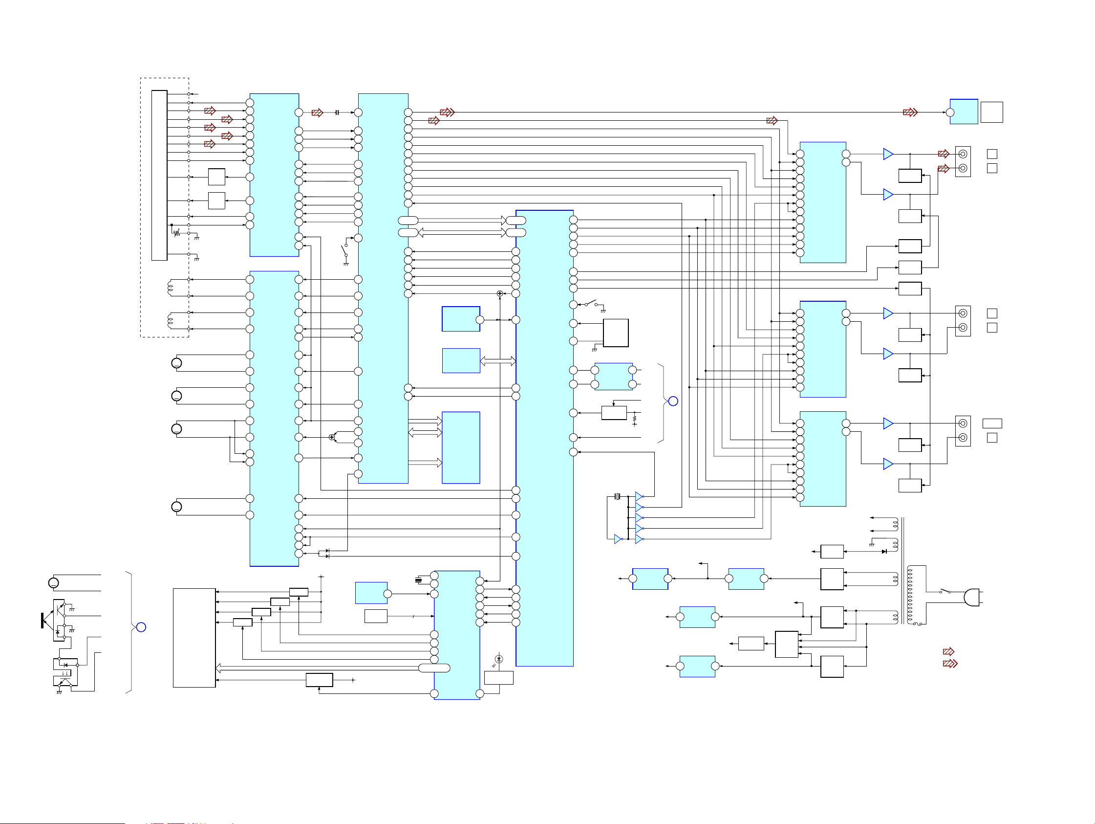
4-1. BLOCK DIAGRAMS
TURN TABLE
MOTOR
PH101
PH102
OPTICAL PICK-UP BLOCK
IC001
19
VC
1
RFIP
14
A
13
B
12
C
11
D
15
E
16
F
25
DVDLD
26
CDLD
24
LDSELO
2
PD
MOTOR/COIL DRIVER
37
DO1+
36
DO1-
35
DO2+
34
DO2-
32
DO3+
31
DO3-
30
DO4+
29
DO4-
28
DO5+
27
DO5-
46
OPIN1-
47
OPIN1+
25
DO6+
24
DO6-
Q822-Q825
FLDRIVER
Q823
Q822
RF AMP
IC712
41TE
42FE
PI
36
33MIRR
TZC
37
DFT
38
45SRD 245
46SWD 246
47SCLK 247
48SDEN 244
LDON
27
VCI
39
SWITCH
IN1+
48
IN1-
1
IN2+
3
4
IN2-
5
OUT2
IN3+
6
IN3-
7 SLDB
IN4+
9
IN4-
10 SLDA
12
IN5+
IN5-
13
45
OPOUT1
1716REV
FWD
PS
39
MUTE12
19
20
21
Q825
D509
+3.3V
FLDRIVER
Q821
MUTE34
MUTE5
Q824
LIMIT
IN
S841-845,
S851-853,855,
S875-871
VCC
6,14
5
3
8
9
2
1
7
10
DVDLD
17
19
15
12
4
FOCUS
COIL
TRACKING
COIL
SLED B
MOTOR
SLED A
MOTOR
SPINDLE
MOTOR
LOADING
MOTOR
M
4
3
2
1
2
3
4
TM-
TM+
DSENS
1
SENSOR
LED
TSENS
1
A5V
VC
RF
A
B
C
D
E
F
CDLD
SW
PD
VR
GND
FCS+
FCS-
TR+
TR-
SLB+
M
SLB-
SLA+
M
SLA-
SPM-
M
SPM+
LOADP
M
LOADN
INDICATION TUBE
FL801
Q001
LD
DRIVE
Q002
LD
DRIVE
5
6
7
8
9-20,32-48
49
IC706
DIGITAL SERVO,
DIGITAL SIGNAL PROCESSOR
DOUT958
19059SIGO
RFAC
200
TEI
201
FEI
202
PI
MIRR
231
TZC
230
DFCTI
229
SSI
SSO
SCK
SCS
234 INLIM
215
FDOP
216
FDON
213
TDOP
214
TDON
203
SEI
220
219
VCO
206
221
MDS0
222
MDP0
204
SP RV
235
FGMODE
IC802
SIRCS
29
+3.3V
RM
KEY
100
PCMD1
96
CDBCK
95
CDLRCK
94
DSAL
83
DSAR
84
DSALS
85
DSARS
86
DSAC
89
DSASW
90
DSPHREFO
78
MCKI
3
21-29 13,15-22A0-8 CA0-8
11-18 4-11D0-7 CD0-7
XINT
32
XCS
33
XWAIT
34
XWR
35
XRD
36
XRST
37
JIT
226
SMUTE
61
MA0-10,BA A0-10,BA
MD0-15 DQ0-15
XRAS,
XCAS,
XMWR,
MCKE,
MMCK,
LDQM,
UDQM
X801
5MHz
1
12
16
7
4
22-19
76-61,58-46
9
8
IC701
RESET
OUT
IC702
EEPROM
IC708
16M SDRAM
RAS,
CAS,
WE,
CKE,
CLK,
LDQM,
UDQM
IC801
DISPLAY CONTROLLER
3X1
4X2
17 SIRCS
ANI0-3
80 FIP0
79 FIP1
78 FIP2
77 FIP3
FIP4-32
45 FIP33
D511
6
6RESET
D801
LED DRIVER
11P23
Q826
MASTER CONTROL
92
XINT0
87
XCS
73
XWAIT
71
XWR
70
XRD
72
XWRST
59
XRST
EPR/B,
XEPCS,
XEWC,
EEPSO,
EEPSI,
EEPSCK
52
JIT
74
SMUTE
38
XLDON
TRAY OUT33
30
TRAY IN
DRV ON
35
36
SP ON
849 IFSISO1
838 IFSOSI1
9112 XIFINTACK
857 IFSCSCK1
9615 XIFCSINTP0
IC705
3SLATR DAC
2SCLK DAC
1SDATA DAC
94MZR
95MZL
L MUTE
98
97R MUTE
100M/2
S001 (TRY POSITION DETECT SWITCH)
25LOAD S0
27LOAD S1
26LOAD S2
39TRMP
40TRMM 2OUT2
29DSENS
30TSENS TSENS
EXTAL
65
ROTARY
ENCODER
IC710
TURN TABULE MOTOR DRIVER
9
RIN
7
FIN
INVERTER
Q701
9812
+1.8V
4OUT1
3.3V
X321
11.2896MHz
56
34
11 10
13 12
IC320
INVERTER
3 1
TM-
TM+
DSENS
SENSOR
LED
IC703
+1.8V REG
+5V
AU+
1
+3.3V
IC950
+5V REG
3 1
IC985
AU+ REG
3 1
3 1
MUTE
IC920
+3.3V REG
MUTE REG
Q961
+12V
RECT
D960,961
4
PDATA
3 PBCK
5 PLRCK
1 DSDL
2 DSDR
20 DBCK
19 DSCK
18 PSCK
17 MS
16 MC
15 MD
14 ZEROR
13 ZEROL
3 PBCK
5 PLRCK
1 DSDL
2 DSDR
20 DBCK
19 DSCK
18 PSCK
17 MS
16 MC
15 MD
3 PBCK
5 PLRCK
1 DSDL
2 DSDR
20 DBCK
19 DSCK
18 PSCK
17 MS
16 MC
15 MD
VFL
IC200
DAC
VOUTL
VOUTR
IC230
DAC
VOUTL 9
VOUTR
IC260
DAC
VOUTL
VOUTR
VFL REG
Q971
RECT
D921-924
RECT
D931-934
RECT
D936,937
IC330
OPTICAL OUT
D OUT
1
IC400(1/2)
AMP
IC400(2/2)
IC430(1/2)
SL
SR
IC430(2/2)
CENTER
SW
IC460(2/2)
VF2
VF1
67
MUTE
Q401,402
AMP
21
MUTE
Q501,502
L MUTE
Q303
R MUTE
Q305
MUTE
Q301
AMP
67
MUTE
Q431,432
AMP
21
MUTE
Q531,532
IC460(1/2)
AMP
67
MUTE
Q462,463
AMP
21
MUTE
Q562,563
T101
POWER TRANSFORMER
D971
9
10
10
9
10
S891
POWER
• Signal Path
J351(1/3)
J351(2/3)
J351(3/3)
DIGITAL
OUT
OPTICAL
L
R
SL
SR
CENTER
SW
: CD
: CD DIGITAL OUT (OPTICAL)
SCD-CE595
88
Page 9
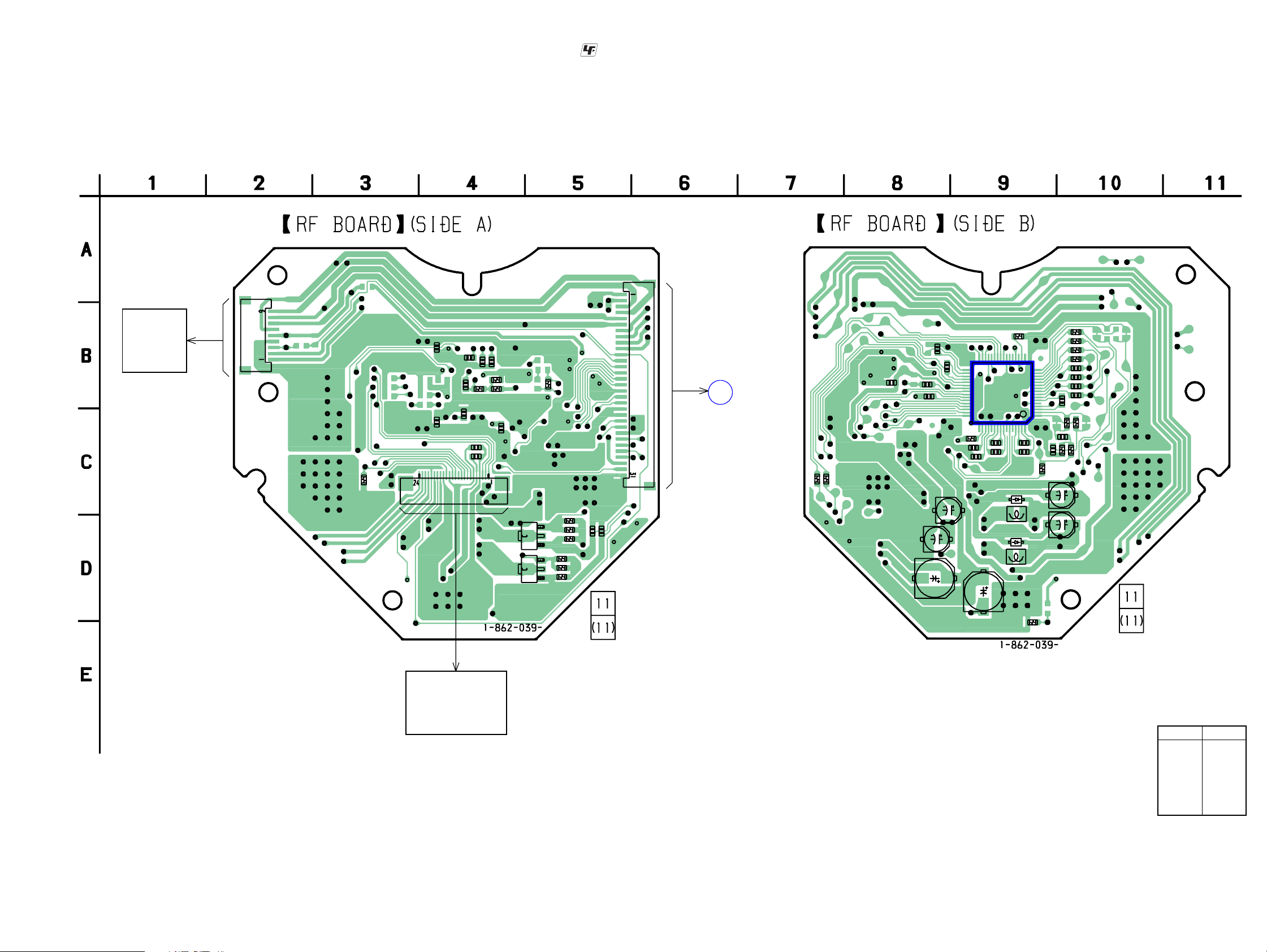
SCD-CE595
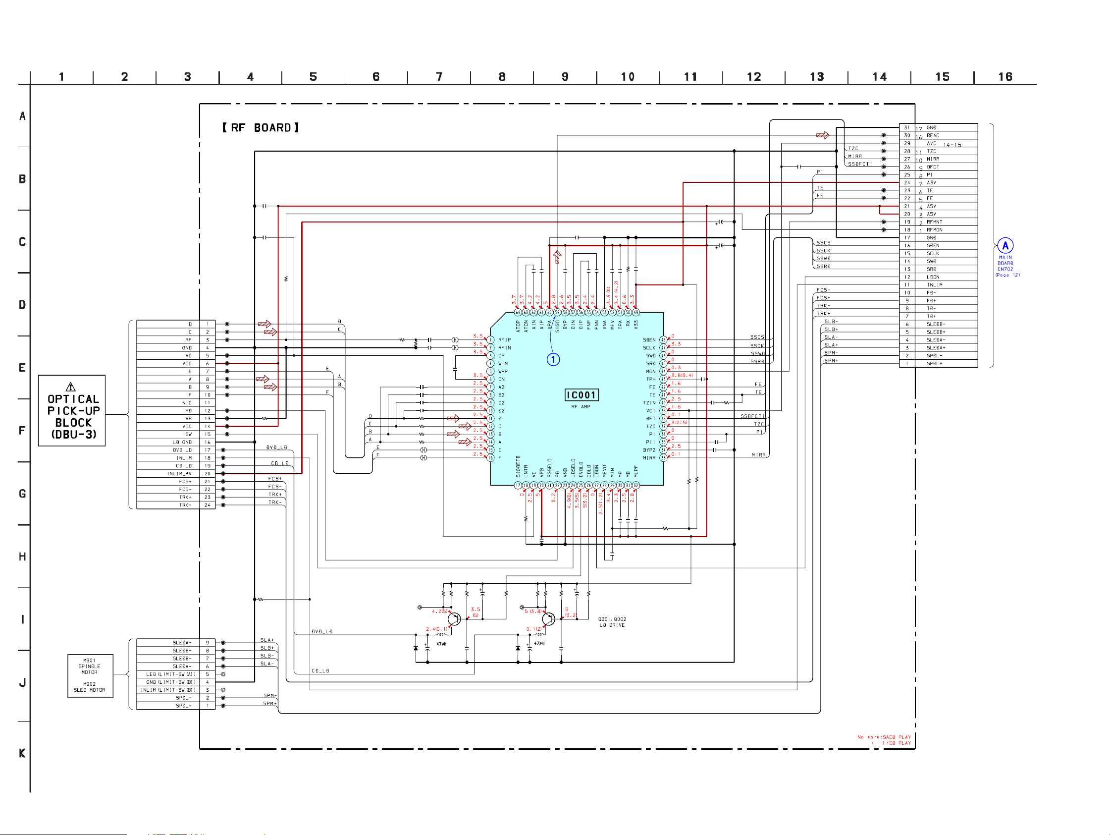
4-2. PRINTED WIRING BOARD — RF SECTION —
OPTICAL
PICK-UP
BLOCK
CN003
(DBU-3)
• See page 7 for Circuit Boards Location. :Uses unleaded solder.
C026
C036
C034
R038
C038
C040
R005
R006
R004
CN002
MAIN BOARD
C039
Q001
Q002
R007
R008
R010
R020
R023
R025
C018
(Page 11)
C024
R003
C027
CN001
C028
C001
C002
A
CN702
R011
R029
C011
C004
C047
C043
C017
C046
C044
C048
C035
R037
C033
IC001
C031
C032
D001
L001
C023
R018
D004
C022
C025
L002
R002
R055
R054
R053
R052
C008
C016
C009
C021
C019
C005
R050
C015
R009
R051
R045
C007
C006
SCD-CE595
M901
SPINDLE MOTOR
M902
SLED MOTOR
R013
• Semiconductor
Location
Ref. No.
D001 C-9
D004 D-9
IC001 C-9
Q001 D-5
Q002 D-5
Location
99
Page 10
SCD-CE595
4-3. SCHEMATIC DIAGRAM — RF SECTION —
CN001
24P
JL003
JL004
JL005
JL006
JL007
JL008
JL009
JL010
JL011
JL012
JL013
JL014
JL015
JL016
JL017
JL018
JL019
JL020
JL021
JL022
JL023
• See page 7 for Waveforms.
C001
0.01
C002
0.01
100
R002
R003
100
C011
0.01
C004
22
R005
100k
6.3V
C044
10
16V
C043
0.1
R004
0
C047
0.1
C048
0.01
C046
0.01
CN002
31PIN
C027
0.01
0.1
0.001
IC001
0.1
C031
0.1
C032
C033
0.1
C025
0.1
C028
SP3726A
0.1
C022
C015
R009
R045
820
220
C016
C005
C006
C007
C008
R052
R053
R054
R055
0.0047
0.0022
0.0022
0.0022
0.0022
0
0
0
JW003
JW004
0.0047
0
JW001
JW002
C019
560p
R018
10k
0.047
C036
C035
12k
R037
0.047
C038
C039
0.01
C040
150p
R038
2.2M
R006
27k
SCD-CE595
CN003
C026
0.01
C017
R008
R007
33
D001
JL001
Q001
2SB1132-T100-QR
C009
L001
10
16V
R013
10k
9P
JL024
JL025
JL026
JL027
JL028
JL031
JL029
JL030
1SS355TE-17
C018
0.001
R010
33
47k
100
6.3V
2SB1132-T100-QR
D004
1SS355TE-17
R011
100
JL002
Q002
R020
R023
33
33
L002
C021
R025
47k
6.3V
C023
100
C024
0.001
10
16V
R029
C034
0.022
100
1010
Page 11
SCD-CE595
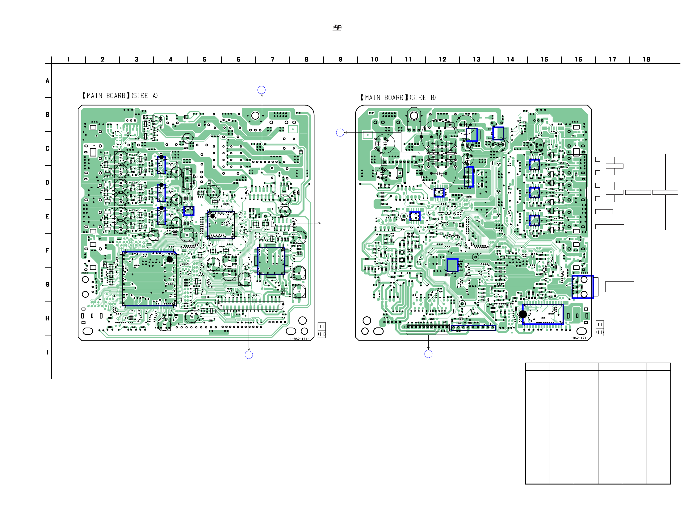
4-4. PRINTED WIRING BOARD — MAIN SECTION —
Q961
D963
R962
R963
R961
C962
Q303
RB302 RB301
Q301 Q305
Q502
RB410
Q402
Q532
RB442
Q432
Q563
RB441
Q463
L341
RB616
L342
C775
C772
TP730
RB617 RB615
C536
C436
C566
C466
C506
C406
C776
R791
C777
R534
R434
C463
R504R404
R564
R464
C504
C503
C534
C433
C564
C563
C403
C533
Q502
C506
C406
C503
R201
IC706
IC200
C502
RB502
C206C208
C402
RB402
IC230
C532
RB532
C236
C432
C238
RB432
C562
RB562
C268 C266
C462
RB462
IC260
C202
TP715
C753
C781C779
C754
C788
L320
C789
C242
C212
C324
D321
C726
C729
C722
C272
TP714
D960
C961
FB201
X321
R330
R328
IC320
R324
R326
C325
RB604
C791
C733
R322
R321
R323
RB602
RB611
RB603
TP713
RB608
• See page 7 for Circuit Boards Location. :Uses unleaded solder.
DISPLAY BOARD
CN801
(Page 16)
B
PT BOARD
CN102
(Page 16)
C
D961
R702
RB601
C705
CN703
R899
RB607
IC712
C970
RB609
R895
Q971
CN701
TP733
R894
C972
C973
R893
R806
R879
R892
D973
C783
C785
C795
R975
C809
D972
R853
C813
R846
not used
C804
C819
C822
R871
RB613
RB606
R851
FL606
C713
RB605
IC705
RB610
C714
C716
C709
C703
C701
R703
D511
RB612
D509
C796
CN702
R857
R872
C901
R976
R977
R978
R979
C830
R880
C820
C787
C794
D937
R701
C829
R886
R874
R973
R804
C971
R972
R820
C702
C704
C821
C828
R971
C935
R888
R889
R876
R885
R866
CN901
STP703
R865
C816
R870
R819
R852
D971
FB710
R869
C832
C817
ETP910
C920
IC701
R861
R878
C825
C815
R860
R877
R897
C800
R831
C793
R858
C814
C932
R818
C808
STP702
D703
C748
C954
C924
STP701
C799
IC950
C953
IC920
C322
C923
C321
C723
C727
C730
C731
Q701
C745
D933
D923
D924
D934
C921
C931
D936
D932
D931
D921
D922
C910
IC702
FB703
R708
C711
C721
R734
C715
C712
C706
IC703
R848
CN704
C806
R815
R828
C749
C734
R752
C746
C750
C934
C742
C743
C736
C739
C740
C741
C737
C738
IC985
C757
C751
C744
C755
C756
C752
R782
C933
R781
R783
C305
C303
C302
IC400
IC430
IC460
R202
C758
C782
C759
C464
C762
C434
C760
C201
C761
C362C404
C364
C366
C763
C764
C767
C768
C769
C771
C780
IC708
C535
C435
C465
C770
C565
C766
C778
C505
C405
C765
Q462
R467
Q401
Q501
Q531
Q431
Q562
R567
R468
R509
R409
R437
R537
R507
C281
R407
R568
R508
R408
R538
R438
R569
R511
R411
R539
R439
R469
C351
C331
IC330
J351
L
FRONT
R
L
SURR 5.1CH OUT ANALOG
R
CENTER
SUB WOOFER
OPTICAL OUT
(DIGITAL CD)
IC710
SCD-CE595
A
RF BOARD
CN002
(Page 9)
D
MD-94 BOARD
CN001
(Page 18)
• Semiconductor Location
Ref. No.
D321 E-4
D509 G-6
D511 E-6
D703 H-13
D921 C-12
D922 C-12
D923 C-12
D924 C-12
D931 C-12
D932 C-12
D933 C-12
D934 C-12
D936 B-12
D937 C-10
D960 B-4
D961 C-8
D963 B-4
D971 D-11
D972 D-8
Location
Ref. No.
IC200 C-4
IC230 D-4
IC260 E-4
IC320 S-5
IC330 G-16
IC400 D-15
IC430 D-15
IC460 E-15
IC701 E-11
IC702 D-12
IC703 F-12
IC705 E-5
IC706 G-3
IC708 H-15
IC710 H-13
IC712 F-7
IC920 D-13
IC950 B-13
IC985 B-14
Location
Ref. No.
Location
Q301 C-3
Q303 C-3
Q305 C-3
Q401 C-15
Q402 D-2
Q431 D-15
Q432 E-2
Q462 E-15
Q463 E-2
Q501 C-15
Q502 C-2
Q531 D-15
Q532 D-2
Q562 E-15
Q563 E-2
Q701 H-13
Q961 B-3
Q971 D-7
D973 D-8
1111
Page 12
SCD-CE595
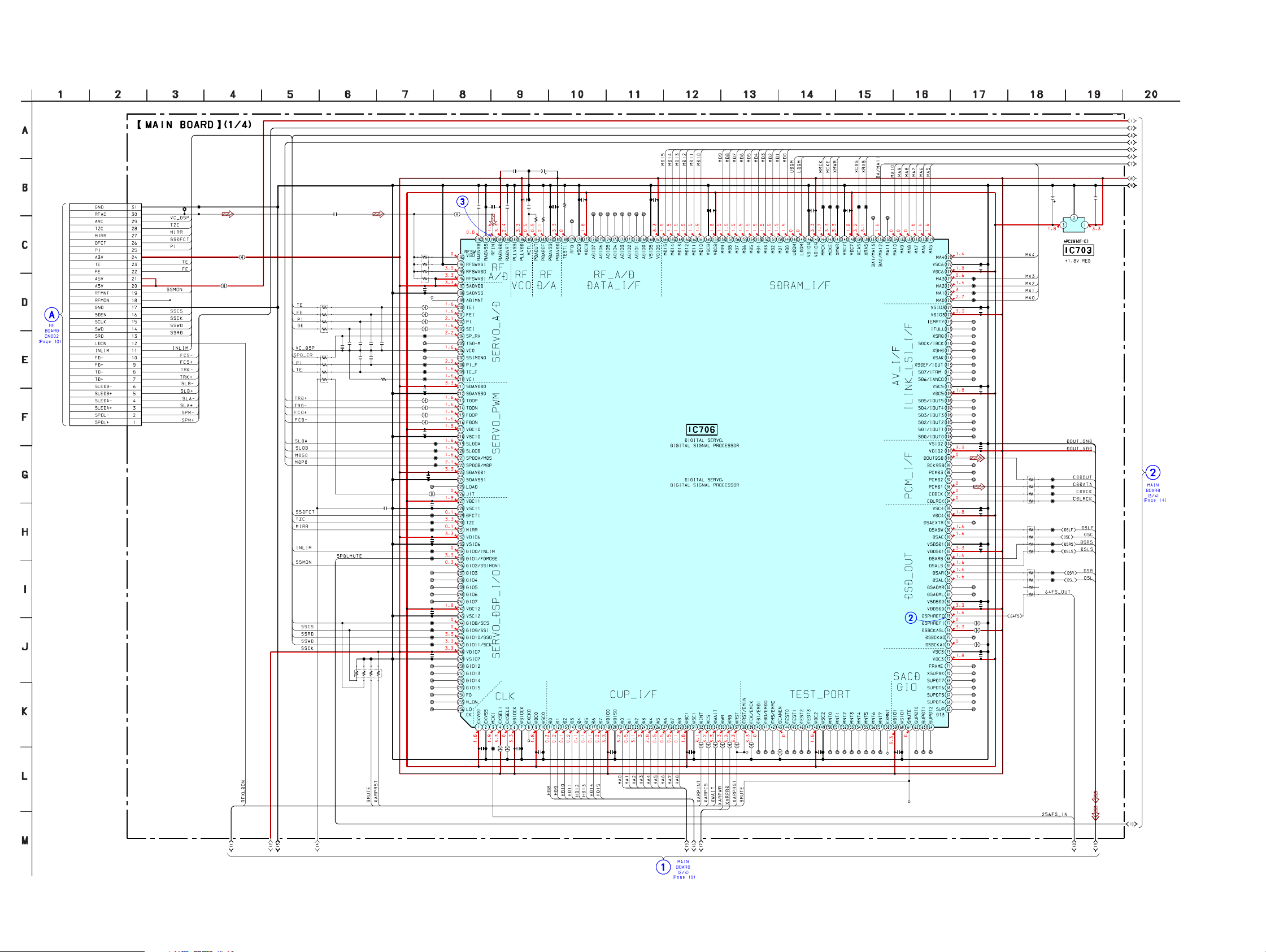
4-5. SCHEMATIC DIAGRAM — MAIN SECTION (1/4) —
CN702
31P
CL721
STP702
CL724
XX
CL723
SL897
SL896
• See page 7 for Waveforms.
C733
0.047
RB604
4.7k
C736
RB603
RB602
470
1
C730
C723
C727
0.0047
0.0047
C729
0.001
0.1
C726
C722
0.001
R752
RB613
0
C734
0.1
10k
1k
TP713
SL774
SL773
SL772
SL771
CL830
C731
0.0047
CL829
CL828
CL754
CL753
CL752
CL751
C743
SL778
SL777
SL776
SL775
C742
CL834
CL833
CL832
CL831
0.1
C741
CL767
SL770
0.1
C740
CL827
CL826
CL825
0.1
C739
CL824
CL823
CL766
CL765
CL764
CL763
CL762
0.1
C738
CL822
CL821
CL820
CL819
0.1
C737
CL761
CL760
CL759
CL758
CL757
CL756
CL755
C754
C789
220
0.1
4V
RB617
RB616
RB615
C714
220
4V
470
CL873
CL872
CL871
CL870
470
CL869
CL867
CL866
CL865
CL864
470
C746
0.1
0.1
C745
0.1
SL798
0.1
0.1
0.1
C751
0.1
100p
1k
C788
C749
47k
R781
R782
C755
0.1
0.1
R783
10k
C753
CL835
CL836
CL837
CL838
CL839
CL840
CL841
C757
0.1
CL842
CL843
IC706
CXD2754Q
256-QFP(0.4)
0.1
C759
0.1
C761
CL844
CL845
CL846
0.1
CL771
CL770
CL848
CL847
C762
0.1
C771
CL877
CL876
CL875
CL874
C770
0.1
CL804
CL803
CL802
CL801
CL800
CL799
CL798
CL797
C769
0.1
CL796
CL795
CL794
CL793
CL792
CL791
C768
0.1
CL790
CL789
CL788
CL787
CL786
C767
0.1
0.1
C766
CL785
C765
CL784
0.1
SL871
SL875
CL782
SL872
C764
0.1
CL781
CL780
CL779
CL778
CL777
CL776
CL775
C706
0.1
IC703
SCD-CE595
1
0.1
C750
CL737
SL799
SL800
TP714
C752
C744
1
0.1
C756
0.1
C758
SL837
SL839
SL840
SL841
SL843
TP715
SL845
SL848
CL849
CL850
CL851
SL856
CL852
CL853
CL854
CL855
0.1
C760
CL856
CL857
CL858
CL859
CL860
CL861
CL862
CL863
TP729
0.1
CL774
CL773
CL772
C763
TP730
XX
1212
Page 13

SCD-CE595
4-6. SCHEMATIC DIAGRAM — MAIN SECTION (2/4) —
CN703
13P
FB703
0UH
FB710
0UH
17
15
• See page 20 for IC Block Diagrams. • See page 20 for IC Pin Function Description.
12
RB612
RB606
10k
10k
RB601 RB607
10k 10k
FL606
0UH
C713
100 16V
C715
C721
0.1
40
7
L
0.1
C
8
87
L
C
46
L7
C
2
3
0
1
8
8
8
79
88
8
8
8
8
L
L
L
L
L
C
C
C
C
C
48
7
L
C
R734
R708
CN701
9P
15
100
D511
DAP202UT106
C704
STP703
R707
1k
C705
0.1
R701
0
3
L7
C
R703
C703
0.1
0.1
CL708
1k
C702
1
IC701
M51957BFP-600C
10k
CL710
C701
0.1
R702
10k
10k
CL734
CL731
C712
0.1
C711
0.1
CL891
CL890
CL889
CL888
CL733
CL732
CL743
5
9
73
73
L
L
5
6
C
2
73
L7
L
C
9
0
7
L
C
C
2
8
C
9
3
8
7
0
L
L
32
3
C
C
7
7
L
L
S
S
HD6432238RN51TEV
4
3
9
89
L8
L
C
C
IC705
2
5
1
7
4
4
4
4
7
7
7
L
L
L7
L
C
C
C
C
1
53
2
4
L7
S
5
9
7
7
46
L
L
7
74
S
S
L
SL
S
RB611
10k
2
0
9
57
79
79
75
7
L
L
L
L
S
S
S
S
CL769
CL768
C748
0.1
15
SCD-CE595
IC702
BR9040F-WE2
CL722
CL726
RB605
10k
1313
Page 14

SCD-CE595
4-7. SCHEMATIC DIAGRAM — MAIN SECTION (3/4) —
CL712
CL727
CL713
GND
BA6956AN
FIN
9.3
9.3
C799
0.1
CL711
IC710
VCC
C791
STP701
XX
TABLE_GND
VREF
OUT2
RMF
OUT1
VIN
123456789
5
0
0
0
C808
0.01
47
25V
C806
0.1
TABLE_+12V
R848
R851
2.2K
1K
D703
UDZSTE-175.1B
15
C716
C709
100
220
16V
4V
CL728
CL729
RIN
00 0
R860
0.0015
R878
470k
C825
R877
470k680k
R861
270k
C815
0.015
R858C814
120k0.22
CN704
C796
C793
100
0.1
16V
D509
DAP202UT106
CL818
0.1
12
C775
0.1
CL805
47
R791
CL806
C777
10p
C778
0.1
C780
0.1
C782
0.1
IC708
MSM56V16160F- 8TK7R1
C772
C776
0.1
10
R806
C779
0.1
C781
0.1
CL815
CL814
SL895
SL894
SL893
SL892
SL891
SL898
C795
C794
100
0.1
16V
R880
100k
R820
150k
R819
150k
TP733
XX
R831
10k
R840
100k
C800
0.1
IC712
FAN8035L
C787
0.1
R804
330
R872
10k
1
C785
220
10k
R871
C819
4V
C804
0.1
R852
33k
R897
470k
C832
0.0047
R899
220k
C817
0.001
R870
33k
R869
56k
C816
0.001
R866
33k
R865
56k
R876
R885
C828
15k
82k
C821
100p
C820 R893
220p 120k
C809
C783
100
16V
R853
56k
0.033
R846
56k
33k
R857
C813
0.033
C822
0.068
R874
33k
0.068
C829
82k
R886
220p
RB609
10k
R889
0
R895
56k
R894
56k
R892
120k
15k
C830
100p
R888
TRMP
TRMM
Q701
DTC143TKA
-T146
DSENS
TSENS
RB608
R815
R818
0
0
CL810
CL811
CL809
CL808
CL807
CL816
CL817
47K
CL812
CL813
100
100
0
R828
220
RB618
RB618
47K
47K
11P
S0
S1
S2
SOND
SENSOR LED
TSENS
DSENS
LMLM+
TM+
TM-
1
2
3
4
5
6
7
8
9
10
11
D
MD-94 BOARD
CN001
(Page 19)
SCD-CE595
13
1414
Page 15

SCD-CE595
4-8. SCHEMATIC DIAGRAM — MAIN SECTION (4/4) —
14
C325
100
6.3V
C324
D321
1SS357-TPH3
IC320
SN74LVU04APWR
13
13
SL215
SL216
SL217
SL220
SL201
SL231
SL261
SL262
CL201
R324
100
IC260
DSD1751DBQR
1
22
R326
IC200
DSD1751DBQR
IC230
DSD1751DBQR
CL868
22
R330
22
R328
R323
1k
R321
1M
R322
C322
15p
C321
15p
X321
11.2896M
C212
10
50V
1
1
C208
C206
C242
10
50V
CL244
CL245
1
1
C238
C236
C272
10
50V
CL275
CL274
C268
C266
1
1
• See page 7 for Waveforms.
0
C281
2200p
C404
1
C201
1000
6.3V
FB201
R201
1
C504
0UH
10k
R202
33k
1
C434
1
C534
1
C464
C564
IC985
BA12FP-E2
C934
C933
470
0.1
16V
C953
C954
470
0.1
10V
IC950
BA50BC0FP-
E2
C921
C924
0.1
470
10V
C923
Q305
UN5116-TX
Q303
2SC3624A-
Q531
2SC3624A-
T1L15L16
2SC3624AT1L15L16
2SC3624A-
T1L15L16
Q501
T1L15L16
2SC3624A-
T1L15L16
Q462
Q562
2SC3624A-
T1L15L16
UN5116-TX
2SC3624A-T
1L15L16
Q502
2SC3624A-T
1L15L16
Q432
2SC3624A-
T1L15L16
Q532
2SC3624A-
T1L15L16
Q463
2SC3624A-T
1L15L16
Q563
2SC3624A-T
1L15L16
C305
0.1
R411
100
Q402
RB410
2.2k
RB442
2.2k
C303
0.1
CL302
R409
220
Q401
R509
220
R439
220
Q431
RB441
2.2k
R539
220330
R469
220
R569
220
CL301
C302
0.1
Q301
UN5116-TX
RB301
4.7k
IC400(2/2)
NJM4565M(T
E2)
RB402
C403
6.8k
150p
C402
0.001
C502
0.001
RB502
6.8k
C202
47
IC430(2/2)
6.3V
NJM4565M(T
RB432
C432
6.8k
0.001
C532
RB532
0.001
6.8k
IC430(1/2)
NJM4565M(T
E2)
IC460(2/2)
NJM4565M(T
E2)
C462
RB462
0.001
6.8k
C562
RB562
0.001
6.8k
1
C362
0.1
C503
150p
IC400(1/2)
NJM4565M(T
E2)
E2)
150p
C433
C364
0.1
C533
150p
C366
0.1
150p
C463
C563
150p
IC460(1/2)
NJM4565M(T
E2)
RB302
220k
C406
47 25V
R408
330
C405
0.1
R407
100k
R404
3.3k
R507R504
100k3.3k
C505
0.1
R508 R511
C506
330 100
47 25V
C436
R438
47
25V
330
C435
0.1
R437
R434
100k
3.3k
R537
R534
100k
3.3k
C535
0.1
R538
C536
47
25V
C466
R468
3304725V
C465
0.1
R464
R467
3.3k
100k
R564
R567
3.3k
100k
C565
0.1
R568
C566
330
47
25V
IC920
BA33BC0T
10000
Q961
DTC143TKA-
10V
T146
R963
1k
R962
1k
C962
D960
DAN202UT106
C931
10000
16V
C961
10
50V
1k
D963
UDZSTE -173.0B
R961
0.1
C331
0.1
C932
1SR154-400TE25
470
35V
1SR154-400TE25
1SR154-400TE25
D936
D931
D932
C910
1SR154-400TE25
1SR154-400TE25
C971
47
63V
1SR154-400TE25
1SR154-400TE25
D961
DAN202UT106
0.001
ETP910
EARTH PLATE
D921
D922
1SR154-400TE25
D971
1SR154-400TE25
R972
10k
R971
10k
D937
D933
1SR154-400TE25
D934
1SR154-400TE25
D924
R973
3.3k
UDZSTE-17-33B
C935
1000
16V
C901
0.01
D923
C920
0.01
CN901
8P
17
C970
0.01
13
Q971
2SB1260
D972
R976
R977
D973
UDZSTE-179.1B
C972
10
50V
R975
33k
R978
100
100
22k
C973
R979
22
10k
16V
J351
6P
C351
0.1
CL202
IC330
IC TOTX141L
SCD-CE595
1515
Page 16

SCD-CE595
4-9. PRINTED WIRING BOARD — DISPLAY SECTION —
CN102
LP5
LP6
AMS
.>
PUSH ENTER
S845
R845
M
JW826
LP856
JW830
S852
EX-CHANGE
R852
S853
C
MAIN BOARD
CN901
(Page 11)
R853 R854
DISC SKIP
S855
• See page 7 for Circuit Boards Location. :Uses unleaded solder.
LP4
C101
CN101
LP3
JW820
C827
JW821
R841
R842
S842
H
JW825
FB801
Q826
R856
R857
R858
JW824
C816
JW823
JW822
S844
m
T101
R844
S841
S843
R843
X
x
Q825
C825
R825
JW819
JW817
JW818
C824
Q824
C817
C818
R824
Q823
C823
R817
R818
POWER
R823
R822
JW815
JW816
S891
C822
C813
Q822
C812
C811
C801
R805
C803
CN892
X801
C802
JW814
C891
FL801
JW812
JW813
CN891
IC801
C804
C820
C819
JW806
Q821
R819
R820
R821
R826
JW811
LP2
LP1
JW804
JW810
R821
C805
JW805
JW809
JW808
C806
C821
JW807
R831
C829
C831
C866
JW803
AC IN
JW802
IC802
JW801
C832
R832
CN805
• Semiconductor
Location
Ref. No.
IC801 G-14
IC802 G-18
Q821 G-15
Q822 F-13
Q823 F-12
Q824 F-12
Q825 F-11
Q826 G-10
Location
B
MAIN BOARD
CN703
(Page 11)
CN801
CN804
JW833
JW832
JW831
JW829
JW828
R851
S851
JW827
A
MULTI CHANNEL DECODING
CN814
C833
R834
D801
S875
R874
R873
S874
S873
R872
S872 R871
TIME/TEXT PLAY MODE MULTI/2CH SA-SD/CD MENU
R864
CN813
S864S865
R863
S863
R862
S862
R871
R861
DISC 1DISC 2DISC 3DISC 4DISC 5
S861
SCD-CE595
1616
Page 17

SCD-CE595
4-10. SCHEMATIC DIAGRAM — DISPLAY SECTION —
R871R872R873R874
1k2.2k2.2k4.7k
S875
S8774
S873
S872
S871
DISK5 DISK4 DISK3 DISK2 DISK1
S865
S864
S863
R861R862R863R864
1k2.2k2.2k4.7k
S862
S861
CN813
2P
KEY 0
3
• See page 7 for Waveforms.
KEY 0
3
CN805
2P
IC802
NJL73H400A
C820
0.01 25V
R832
100
C831
47
C832
6.3V
0.01
R831
47
TP126
C804
0.1
R826
10k
TP26
R820
10k
1.6
-30.8
-33
-33
-33
Q821
DTC114EKA-T146
-20
-28
-28
-32
-24
-22
-30
-29
-28
-26.5
C805
-30
0.1
C806
0.1
-31
-31
-33
-22.3
-28.7
-30
IC801
8BT-A
3.3
0.5
3.3
3.3
-31
-31
-31
-31
-31
-31
-31
-31
-31
-31
-31
-30
DTC114EKA-T146
R821 R822 R823 R824 R825
100k 100k 100k 100k 100k
C821
0.001
C829
0.1
C819
0.01
R841
R819
10k
k
k
0
1
10
7
8
1
8
81
R
R
1
.1
0
0.0
0.01
3
8
80
81
817
C
C
C
C816
0.001
C812
0
0.001
Q822
0.001
C813
C811
0.001
R856
FB801
10k
FB
TP5
X801
5MHz
R805
10k
Q823
DTC114EKA
-T146
C822
0.001
S841 S842 S843 S844 S845
S851
Q826
2SC3624A- T1L15L16
C802
0.1
Q824
DTC114EKA
-T146
C823
0.001
R842 R843
1k1k2.2k 2.2k
R851
C824
0.001
*
*
R844
4.7k
R852 R853
2.2k 2.2k
S853
S852
**
R858
82
R857
10k
C801
100
6.3V
Q825
DTC114EKA
-T146
C825
0.001
S852
EXCHANGE
S853
DISCSKIP
R845
10k
C827
0.1
R854
4.7k
S855
ENCORDER
CN804
2P
13
CN801
13P
SCD-CE595
FL801
T101
CN814
2P
C101
0.0022 250V
CN101
C833
R834
D801
SEL5E20C-STP15
S891
C891
0.0022
250V
CN892
2P
2P
CN891
2P
BLUE
0.1 10k
15
CN102
8P
1717
Page 18

SCD-CE595
4-11. PRINTED WIRING BOARD — MD-94 BOARD SECTION —
SE-130 BOARD
PH101
• See page 7 for Circuit Boards Location. :Uses unleaded solder.
M001
TURN TABLE
M
MOTOR
CN102
PH102
MD-94 BOARD
D
CN001
MAIN BOARD
CN704
(Page 11)
CN101
13
(13)
SCD-CE595
ROTARY
ENCODER
LOADING
MOTOR
M
CN003CN004
CN002
13
S001
(13)
1818
Page 19

4-12. SCHEMATIC DIAGRAM — MD-94 BOARD SECTION —
CN001
11P
CN003
3P
SCD-CE595
D
3/4
CN704
14
S001
CN004
2P
CN002
6P
SCD-CE595
CN101
6P
CN102
PH101
RPR-220C1N
PH102
RPI-392
2P
M001
1919
Page 20

SCD-CE595
• IC Block Diagrams
– MAIN Board –
IC701 M51957BFP-600C
NC
8
1
NC
VCC
7
–
+
1.25V
2
IN
• IC Pin Function Description
• MAIN BOARD IC705 HD6432238RN51TEV (SYSTEM CONTROLLER)
Pin No. Pin Name I/O Description
IC702 BR9040F-WF2
1SDATA DAC O Data output to the DAC (IC200)
2 SCLK DAC O Clock output to the DAC (IC200)
OUT
6
C
5
WC
8 7 6 5
GND
DO
DI
3 SLATR DAC O Latch (R-ch) output to the DAC (IC200)
4 to 11 CD0 to 7 I/0 Data Bus to the Digital Servo Processor (IC706)
4096bit
EEPROM ARRAY
8bit
ADDRESS
DECODER
3
4
NC
GND
8bit
ADDRESS
BUFFER
16bit
R/W
AMP
16bit
DATA
REGISTER
HIGH VOLTAGE
GENERATOR
COMMAND
REGISTER
WRITE
DISABLE
POWER
SUPPLY
VOLTAGE
DETECTOR
COMMAND DECODE
CONTROL CLOCK
GENERATION
12 CVCC — Power supply terminal (+3.3V)
13 CA0 O Address Bus to the Digital Servo Processor (IC706)
14 VSS — Ground terminal
15 to 22 CA1 to 8 O Address Bus to the Digital Servo Processor (IC706)
23 PB1 — Not used (open)
24 PB2 — Not used (open)
25 LOAD S0 I DISK cyacking select (SO)
26 LOAD S1 I TRAY (S2:OPEN)
27 LOAD S2 I TRAY (S1:TURN)
28 TSENS I T sens signal input
29 DSENS I DISK sens signal input
1 2 3 4
R/B
VCC
CS
SK
30 TRAY IN O TRAY in control output to the Motor Driver (IC712)
31 RS232CTX O PC serial signal
32 RS232CRX I PC serial signal
33 TRAY OUT O TRAY out control output to the Motor Driver (IC712)
34 P10 — Not used (open)
35 DRV ON O Driver mute output to the Motor Driver (IC712)
36 SP ON O Spindle mute output to the Motor Driver (IC712)
37 P13 — Not used (open)
38 XLDON O LD ON/OFF output to the Motor Driver (IC712)
39 TRMP O Table control (+Clockwise) output to the TMD (IC710)
40 TRMM O Table control (-Counterclock) output to the TMD (IC710)
41 P17 — Not used (open)
42 AVSS — Ground terminal
43 DIAO I Test Mode input
44 P96 — Ground terminal
45 to 50 P47 to P42 — Ground terminal
51 MODEL I Model check (L:1Hi,Mi:5Es,H:5 Hi)
52 JIT I Waltz jetter select
53 VREF I Reference voltage
54 AVCC — Power supply terminal (+3.3V)
55 MD0 I Muving mode control 0
56 MD1 I Muving mode control 1
57 OSC2 — Not used (open)
58 OSC1 — Ground terminal
59 XRST O System reset
60 XNMI I NMI input (fixed at “H”)
61 XSTBY I Standby input (fixed at “H”)
62 VCC — Power supply terminal (+3.3V)
63 XTAL — Not used (open)
64 VSS1 — Ground terminal
65 EXTAL I External clock input
SCD-CE595
2020
Page 21

Pin No. Pin Name I/O Description
66 FEW I Flash writing Enable
67 MD2 I Muving mode control 2
68 PF7 — Not used (open)
69 AS — Not used (open)
70 XDR O Reed sycle signal
71 XWR O Write sycle signal
72 XWRST O Waltz reset signal output
73 XWAIT I Bus sycle wait signal input
74 SMUTE O Waltz smute signal output
75 EPR/B I Read/Busy signal input from the EEPROM (IC702)
76 XEPCE O XCS signal output to the EEPROM (IC702)
77 XEWC O XWC signal output to the EEPROM (IC702)
78 P32 O Not used (open)
79 EEPS0 O Communication signal to the EEPROM (IC702)
80 EEPS1 I Communication signal from the EEPROM (IC702)
81 EEPSC O Communication signal to the EEPROM (IC702)
82 P36 — Not used (open)
83 IFS0 O Communication signal to the IS CON (IC801)
84 IFS1 I Communication signal from the IS CON (IC801)
85 IFSCK O Communication signal to the IS CON (IC801)
86 P74 — Not used (open)
87 XCS O WALTZ chip select
88 P72 — Not used (open)
89 P71 — Not used (open)
90 P70 — Not used (open)
91 XIFINT I ACK input signal from the IS CON (IC801)
92 XINTO I WALTZ input from the Digital Servo Processor (IC706)
93 PG2 — Ground terminal
94 MZR I ZEROR input signal from DAC (IC200)
95 MZL I ZEROL input signal from DAC (IC200)
96 XIFCS O Chip select to the IS CON (IC801)
97 R MUTE O Rch mute signal output
98 L MUTE O Lch mute signal output
99 INIT DAC O DAC int output
100 M/2 O Mch mute control output (surr/Cntr/Sw)
SCD-CE595
21
Page 22

SCD-CE595
Ver. 1.3
NOTE:
• -XX and -X mean standardized parts, so they
may have some difference from the original
one.
• Items marked “*” are not stocked since they
are seldom required for routine service.
Some delay should be anticipated when
ordering these items.
5-1. MAIN SECTION
SECTION 5
EXPLODED VIEWS
• The mechanical parts with no reference
number in the exploded views are not supplied.
•Abbreviation
CND : Canadian model
2
The components identified by mark 0 or
dotted line with mark 0 are critical for safety .
Replace only with part number specified.
Les composants identifiés par une marque 0
sont critiques pour la sécurité.
Ne les remplacer que par une pièce portant le
numéro spécifié.
4
front panel section
1
5
2
chassis section
#1
Ref. No. Part No. Description Remark
1 X-4956-436-1 PANEL ASSY, LOADING
2 3-363-099-02 SCREW (CASE 3 TP2)
22
Ref. No. Part No. Description Remark
4 4-951-620-01 SCREW (2.6X8), +BVTP
5 3-073-127-22 CASE, UPPER
#1 7-685-872-09 SCREW +BVTT 3X8
Page 23

5-2. FRONT PANEL SECTION
3
SCD-CE595
not supplied
54
#3
not supplied
52
53
#3
not supplied
#
55
56
#3
51
not supplied
Ref. No. Part No. Description Remark Ref. No. Part No. Description Remark
51 X-4956-434-1 PANEL ASSY, FRONT (US,CND)
51 X-4956-435-1 PANEL ASSY, FRONT (AEP,UK)
52 3-354-981-11 SPRING (SUS), RING
53 4-232-622-01 KNOB (AMS)
54 4-255-244-01 BUTTON, POWER
55 A-4752-651-A DISPLAY BOARD, COMPLETE
56 1-828-334-11 WIRE (FLAT TYPE) (13 CORE)
#3 7-685-646-79 SCREW +BVTP 3X8 TYPE2 IT-3
23
Page 24

SCD-CE595
5-3. CHASSIS SECTION
#1
#1
104
103
105
CD mechanism section
(CDM79C-DVBU51)
not supplied
#2
101
102
107
#4
not supplied
106
T101
#6
#6
Ref. No. Part No. Description Remark Ref. No. Part No. Description Remark
101 X-2022-049-1 FOOT ASSY
102 4-977-358-01 CUSHION
* 103 3-703-244-00 BUSHING (2104), CORD
0 104 1-777-071-43 CORD, POWER (AEP,UK)
0 104 1-783-531-32 CORD, POWER (US,CND)
105 3-704-515-32 SCREW (BV/RING)
106 A-4752-598-A MAIN BOARD, COMPLETE
107 4-951-620-01 SCREW (2.6X8), +BVTP
0 T101 1-443-286-11 TRANSFORMER, POWER (US,CND)
0 T101 1-443-287-11 TRANSFORMER, POWER (AEP,UK)
#1 7-685-872-09 SCREW +BVTT 3X8
#2 7-685-535-19 SCREW +BTP 2.6X10 TYPE2 N-S
#4 7-682-544-04 SCREW +P 3X3
#6 7-685-534-19 SCREW +BTP 2.6X8 TYPE2 N-S
The components identified by
mark 0 or dotted line with mark
0 are critical for safety.
Replace only with part number
specified.
Les composants identifiés par
une marque 0 sont critiques
pour la sécurité.
Ne les remplacer que par une
pièce portant le numéro spécifié.
24
Page 25

5-4. CD MECHANISM SECTION (1)
)
(CDM79C-DVBU51)
SCD-CE595
Ver. 1.2
157
156
153
155
#4
not
supplied
#6
#6
not
supplied
152
154
not
supplied
#6
#6
151
158
151
CD mechanism section (2
(CDM79C-DVBU51)
Ref. No. Part No. Description Remark Ref. No. Part No. Description Remark
151 3-074-737-01 PLATE (GUIDE)
152 A-6060-642-A SE-130 BOARD, COMPLETE
153 3-074-716-01 TABLE
154 A-6060-640-A UNIT ASSY, TD
155 3-074-725-01 BELT, TD
156 3-074-717-01 TRAY
157 4-218-252-52 SCREW (+PTPWH M2.6), FLOATING
158 1-823-921-11 FMS-18
#4 7-682-544-04 SCREW +P 3X3
#6 7-685-534-19 SCREW +BTP 2.6X8 TYPE2 N-S
25
Page 26

SCD-CE595
5-5. CD MECHANISM SECTION (2)
(CDM79C-DVBU51)
210
209
208
RE901
211
212
201
214
215
216
not
supplied
217
#2
not
supplied
204
not supplied
M901
205
206
213
218
not supplied
219
220
#8
207
not supplied
203
202
#7
201
Ref. No. Part No. Description Remark Ref. No. Part No. Description Remark
201 4-218-252-52 SCREW (+PTPWH M2.6), FLOATING
202 3-074-744-01 GEAR (LOADING A)
203 3-074-745-01 BELT (LOADING)
204 3-074-742-01 GEAR (SHAFT)
205 4-951-619-01 CUSHION (A)
206 3-074-735-01 GEAR (IDOLER)
207 1-829-172-11 WIRE (FLAT TYPE) (31 CORE)
208 3-074-741-01 GEAR (LOADING B)
209 3-074-738-01 GEAR (SWING)
210 3-074-739-01 COLLAR (SWING)
211 3-016-533-01 WASHER (FR), STOPPER
212 3-074-740-01 GEAR (LOADING C)
213 3-074-736-01 GEAR (CHUCK)
#8
214 4-981-923-01 SCREW (M), STEP
215 3-053-847-31 INSULATOR
0 216 A-1067-676-A DEVICE, OPTICAL (DBU-3)
217 A-4736-882-A CHUCK ASSY
218 1-824-106-12 CABLE, FLEXIBLE FLAT (24 CORE)
219 X-4955-252-3 HOLDER (BU) ASSY
220 A-4750-527-A RF BOARD, COMPLETE
M901 1-541-632-12 MOTOR, DC
RE901 1-418-746-11 ENCODER, ROTARY
#2 7-685-535-19 SCREW +BTP 2.6X10 TYPE2 N-S
#7 7-621-259-25 SCREW +P 2.6X4
#8 7-685-534-19 SCREW +BTP 2.6X8 TYPE2 N-S
The components identified by
mark 0 or dotted line with mark
0 are critical for safety.
Replace only with part number
specified.
Les composants identifiés par
une marque 0 sont critiques
pour la sécurité.
Ne les remplacer que par une
pièce portant le numéro spécifié.
26
Page 27

SCD-CE595
SECTION 6
ELECTRICAL PARTS LIST
NOTE:
• Due to standardization, replacements in the
parts list may be different from the parts
specified in the diagrams or the components
used on the set.
• -XX and -X mean standardized parts, so they
may have some difference from the original
one.
• Items marked “*” are not stocked since they
are seldom required for routine service.
Some delay should be anticipated when
ordering these items.
• CAPACITORS
uF: µF
Ref. No. Part No. Description Remark Ref. No. Part No. Description Remark
A-4752-651-A DISPLAY BOARD, COMPLETE
************************
4-949-935-41 CUSHION (FL)
< CAPACITOR >
C801 1-124-584-00 ELECT 100uF 20% 6.3V
C802 1-164-156-11 CERAMIC CHIP 0.1uF 25V
C803 1-164-156-11 CERAMIC CHIP 0.1uF 25V
C804 1-164-156-11 CERAMIC CHIP 0.1uF 25V
C805 1-164-156-11 CERAMIC CHIP 0.1uF 25V
C806 1-165-319-11 CERAMIC CHIP 0.1uF 50V
C811 1-162-964-11 CERAMIC CHIP 0.001uF 10% 50V
C812 1-162-964-11 CERAMIC CHIP 0.001uF 10% 50V
C813 1-162-964-11 CERAMIC CHIP 0.001uF 10% 50V
C816 1-162-964-11 CERAMIC CHIP 0.001uF 10% 50V
C817 1-162-970-11 CERAMIC CHIP 0.01uF 10% 25V
C818 1-162-970-11 CERAMIC CHIP 0.01uF 10% 25V
C819 1-162-970-11 CERAMIC CHIP 0.01uF 10% 25V
C820 1-162-970-11 CERAMIC CHIP 0.01uF 10% 25V
C821 1-162-964-11 CERAMIC CHIP 0.001uF 10% 50V
C822 1-162-964-11 CERAMIC CHIP 0.001uF 10% 50V
C823 1-162-964-11 CERAMIC CHIP 0.001uF 10% 50V
C824 1-162-964-11 CERAMIC CHIP 0.001uF 10% 50V
C825 1-162-964-11 CERAMIC CHIP 0.001uF 10% 50V
C827 1-165-319-11 CERAMIC CHIP 0.1uF 50V
C829 1-165-319-11 CERAMIC CHIP 0.1uF 50V
C831 1-124-589-11 ELECT 47uF 20% 6.3V
C832 1-162-970-11 CERAMIC CHIP 0.01uF 10% 25V
< CONNECTOR >
CN801 1-779-281-11 CONNECTOR, FFC (LIF (NON-ZIF)) 13P
< FERRITE BEAD >
FB801 1-414-595-11 INDUCTOR, FERRITE BEAD
< FLUORESCENT INDICATOR TUBE >
FL801 1-518-992-11 INDICATOR TUBE, FLUORESCENT
< IC >
IC801 6-804-318-01 IC uPD780232GC-706-8BT-A
IC802 8-759-826-33 IC NJL73H400A ( )
• RESISTORS
All resistors are in ohms.
METAL: Metal-film resistor.
METAL OXIDE: Metal oxide-film resistor.
F: nonflammable
• COILS
uH: µH
• SEMICONDUCTORS
In each case, u: µ, for example:
uA. . : µA. . uPA. . : µPA. .
uPB. . : µPB. . uPC. . : µPC. .
uPD. . : µPD. .
•Abbreviation
CND : Canadian model
Q821 8-729-027-43 TRANSISTOR DTC114EKA-T146
Q822 8-729-027-43 TRANSISTOR DTC114EKA-T146
Q823 8-729-027-43 TRANSISTOR DTC114EKA-T146
Q824 8-729-027-43 TRANSISTOR DTC114EKA-T146
Q825 8-729-027-43 TRANSISTOR DTC114EKA-T146
Q826 8-729-141-73 TRANSISTOR 2SC3624A-T1L15L16
R805 1-216-833-11 METAL CHIP 10K 5% 1/10W
R817 1-216-833-11 METAL CHIP 10K 5% 1/10W
R818 1-216-833-11 METAL CHIP 10K 5% 1/10W
R819 1-216-833-11 METAL CHIP 10K 5% 1/10W
R820 1-216-833-11 METAL CHIP 10K 5% 1/10W
R821 1-216-845-11 METAL CHIP 100K 5% 1/10W
R822 1-216-845-11 METAL CHIP 100K 5% 1/10W
R823 1-216-845-11 METAL CHIP 100K 5% 1/10W
R824 1-216-845-11 METAL CHIP 100K 5% 1/10W
R825 1-216-845-11 METAL CHIP 100K 5% 1/10W
R826 1-216-833-11 METAL CHIP 10K 5% 1/10W
R831 1-216-805-11 METAL CHIP 47 5% 1/10W
R832 1-216-809-11 METAL CHIP 100 5% 1/10W
R841 1-216-821-11 METAL CHIP 1K 5% 1/10W
R842 1-216-825-11 METAL CHIP 2.2K 5% 1/10W
R843 1-216-825-11 METAL CHIP 2.2K 5% 1/10W
R844 1-216-829-11 METAL CHIP 4.7K 5% 1/10W
R845 1-216-833-11 METAL CHIP 10K 5% 1/10W
R851 1-216-821-11 METAL CHIP 1K 5% 1/10W
R852 1-216-825-11 METAL CHIP 2.2K 5% 1/10W
R853 1-216-825-11 METAL CHIP 2.2K 5% 1/10W
R854 1-216-829-11 METAL CHIP 4.7K 5% 1/10W
R856 1-216-833-11 METAL CHIP 10K 5% 1/10W
R857 1-216-833-11 METAL CHIP 10K 5% 1/10W
R858 1-216-808-11 METAL CHIP 82 5% 1/10W
S841 1-762-875-21 SWITCH, KEYBOARD (x)
S842 1-762-875-21 SWITCH, KEYBOARD (H)
S843 1-762-875-21 SWITCH, KEYBOARD (X)
S844 1-762-875-21 SWITCH, KEYBOARD (m)
S845 1-762-875-21 SWITCH, KEYBOARD (M)
S851 1-762-875-21 SWITCH, KEYBOARD (A)
S852 1-762-875-21 SWITCH, KEYBOARD (EX-CHANGE)
When indicating parts by reference number,
please include the board name.
The components identified by mark 0 or
dotted line with mark 0 are critical for safety .
Replace only with part number specified.
Les composants identifiés par une marque 0
sont critiques pour la sécurité.
Ne les remplacer que par une pièce portant le
numéro spécifié.
• Accessories are given in the last of this parts
list.
< TRANSISTOR >
< RESISTOR >
< SWITCH >
DISPLAY
27
Page 28

SCD-CE595
DISPLAY MAINKEY LED
Ref. No. Part No. Description Remark Ref. No. Part No. Description Remark
S853 1-762-875-21 SWITCH, KEYBOARD (DISC SKIP)
S855 1-478-268-11 ENCODER, ROTARY
(. AMS >)(PUSH ENTER)
< VIBRATOR >
X801 1-795-058-21 VIBRATOR, CERAMIC 5MHz
************************************************************
1-862-173-11 KEY BOARD
**********
< CONNECTOR >
CN813 1-506-468-11 PIN, CONNECTOR 3P
< RESISTOR >
R861 1-216-821-11 METAL CHIP 1K 5% 1/10W
R862 1-216-825-11 METAL CHIP 2.2K 5% 1/10W
R863 1-216-825-11 METAL CHIP 2.2K 5% 1/10W
R864 1-216-829-11 METAL CHIP 4.7K 5% 1/10W
R871 1-216-821-11 METAL CHIP 1K 5% 1/10W
R872 1-216-825-11 METAL CHIP 2.2K 5% 1/10W
R873 1-216-825-11 METAL CHIP 2.2K 5% 1/10W
R874 1-216-829-11 METAL CHIP 4.7K 5% 1/10W
< SWITCH >
S861 1-762-875-21 SWITCH, KEYBOARD (MENU)
S862 1-762-875-21 SWITCH, KEYBOARD (SA-CD/CD)
S863 1-762-875-21 SWITCH, KEYBOARD (MULITI/2CH)
S864 1-762-875-21 SWITCH, KEYBOARD (PLAY MODE)
S865 1-762-875-21 SWITCH, KEYBOARD (TIME/TEXT)
S871 1-762-875-21 SWITCH, KEYBOARD (DISC 1)
S872 1-762-875-21 SWITCH, KEYBOARD (DISC 2)
S873 1-762-875-21 SWITCH, KEYBOARD (DISC 3)
S874 1-762-875-21 SWITCH, KEYBOARD (DISC 4)
S875 1-762-875-21 SWITCH, KEYBOARD (DISC 5)
************************************************************
1-862-174-11 LED BOARD
**********
< CAPACITOR >
C833 1-164-156-11 CERAMIC CHIP 0.1uF 25V
< CONNECTOR >
CN814 1-506-481-11 PIN, CONNECTOR 2P
< DIODE >
D801 6-500-647-01 DIODE SEL5E20C-STP15
< RESISTOR >
R834 1-216-833-11 METAL CHIP 10K 5% 1/10W
************************************************************
A-4752-598-A MAIN BOARD, COMPLETE
*********************
< CAPACITOR >
C201 1-126-916-11 ELECT 1000uF 20% 6.3V
C202 1-126-205-11 ELECT CHIP 47uF 20% 6.3V
C206 1-115-156-11 CERAMIC CHIP 1uF 10V
C208 1-115-156-11 CERAMIC CHIP 1uF 10V
C212 1-128-991-21 ELECT CHIP 10uF 20% 50V
C236 1-115-156-11 CERAMIC CHIP 1uF 10V
C238 1-115-156-11 CERAMIC CHIP 1uF 10V
C242 1-128-991-21 ELECT CHIP 10uF 20% 50V
C266 1-115-156-11 CERAMIC CHIP 1uF 10V
C268 1-115-156-11 CERAMIC CHIP 1uF 10V
C272 1-128-991-21 ELECT CHIP 10uF 20% 50V
C281 1-162-966-11 CERAMIC CHIP 0.0022uF 10% 50V
C302 1-164-156-11 CERAMIC CHIP 0.1uF 25V
C303 1-164-156-11 CERAMIC CHIP 0.1uF 25V
C305 1-164-156-11 CERAMIC CHIP 0.1uF 25V
C321 1-162-917-11 CERAMIC CHIP 15PF 5% 50V
C322 1-162-917-11 CERAMIC CHIP 15PF 5% 50V
C324 1-115-156-11 CERAMIC CHIP 1uF 10V
C325 1-126-206-11 ELECT CHIP 100uF 20% 6.3V
C331 1-164-156-11 CERAMIC CHIP 0.1uF 25V
C351 1-164-156-11 CERAMIC CHIP 0.1uF 25V
C362 1-164-156-11 CERAMIC CHIP 0.1uF 25V
C364 1-164-156-11 CERAMIC CHIP 0.1uF 25V
C366 1-164-156-11 CERAMIC CHIP 0.1uF 25V
C402 1-115-416-11 CERAMIC CHIP 0.001uF 5% 25V
C403 1-164-217-11 CERAMIC CHIP 150PF 5% 50V
C404 1-115-156-11 CERAMIC CHIP 1uF 10V
C405 1-107-826-11 CERAMIC CHIP 0.1uF 10% 16V
C406 1-128-992-21 ELECT CHIP 47uF 20% 25V
C432 1-115-416-11 CERAMIC CHIP 0.001uF 5% 25V
C433 1-164-217-11 CERAMIC CHIP 150PF 5% 50V
C434 1-115-156-11 CERAMIC CHIP 1uF 10V
C435 1-107-826-11 CERAMIC CHIP 0.1uF 10% 16V
C436 1-128-992-21 ELECT CHIP 47uF 20% 25V
C462 1-115-416-11 CERAMIC CHIP 0.001uF 5% 25V
C463 1-164-217-11 CERAMIC CHIP 150PF 5% 50V
C464 1-115-156-11 CERAMIC CHIP 1uF 10V
C465 1-107-826-11 CERAMIC CHIP 0.1uF 10% 16V
C466 1-128-992-21 ELECT CHIP 47uF 20% 25V
C502 1-115-416-11 CERAMIC CHIP 0.001uF 5% 25V
C503 1-164-217-11 CERAMIC CHIP 150PF 5% 50V
C504 1-115-156-11 CERAMIC CHIP 1uF 10V
C505 1-107-826-11 CERAMIC CHIP 0.1uF 10% 16V
C506 1-128-992-21 ELECT CHIP 47uF 20% 25V
C532 1-115-416-11 CERAMIC CHIP 0.001uF 5% 25V
C533 1-164-217-11 CERAMIC CHIP 150PF 5% 50V
C534 1-115-156-11 CERAMIC CHIP 1uF 10V
C535 1-107-826-11 CERAMIC CHIP 0.1uF 10% 16V
C536 1-128-992-21 ELECT CHIP 47uF 20% 25V
C562 1-115-416-11 CERAMIC CHIP 0.001uF 5% 25V
C563 1-164-217-11 CERAMIC CHIP 150PF 5% 50V
C564 1-115-156-11 CERAMIC CHIP 1uF 10V
C565 1-107-826-11 CERAMIC CHIP 0.1uF 10% 16V
C566 1-128-992-21 ELECT CHIP 47uF 20% 25V
C701 1-164-156-11 CERAMIC CHIP 0.1uF 25V
C702 1-125-837-91 CERAMIC CHIP 1uF 10% 6.3V
C703 1-164-156-11 CERAMIC CHIP 0.1uF 25V
C704 1-164-156-11 CERAMIC CHIP 0.1uF 25V
C705 1-164-156-11 CERAMIC CHIP 0.1uF 25V
28
Page 29

SCD-CE595
MAIN
Ref. No. Part No. Description Remark Ref. No. Part No. Description Remark
C706 1-164-156-11 CERAMIC CHIP 0.1uF 25V
C709 1-126-246-11 ELECT CHIP 220uF 20% 4V
C711 1-164-156-11 CERAMIC CHIP 0.1uF 25V
C712 1-164-156-11 CERAMIC CHIP 0.1uF 25V
C713 1-117-681-11 ELECT CHIP 100uF 20% 16V
C714 1-126-246-11 ELECT CHIP 220uF 20% 4V
C715 1-164-156-11 CERAMIC CHIP 0.1uF 25V
C716 1-117-681-11 ELECT CHIP 100uF 20% 16V
C721 1-164-156-11 CERAMIC CHIP 0.1uF 25V
C722 1-107-826-11 CERAMIC CHIP 0.1uF 10% 16V
C723 1-125-837-91 CERAMIC CHIP 1uF 10% 6.3V
C726 1-162-964-11 CERAMIC CHIP 0.001uF 10% 50V
C727 1-162-968-11 CERAMIC CHIP 0.0047uF 10% 50V
C729 1-162-964-11 CERAMIC CHIP 0.001uF 10% 50V
C730 1-162-968-11 CERAMIC CHIP 0.0047uF 10% 50V
C731 1-162-968-11 CERAMIC CHIP 0.0047uF 10% 50V
C733 1-165-176-11 CERAMIC CHIP 0.047uF 10% 16V
C734 1-107-826-11 CERAMIC CHIP 0.1uF 10% 16V
C736 1-164-156-11 CERAMIC CHIP 0.1uF 25V
C737 1-164-156-11 CERAMIC CHIP 0.1uF 25V
C738 1-164-156-11 CERAMIC CHIP 0.1uF 25V
C739 1-164-156-11 CERAMIC CHIP 0.1uF 25V
C740 1-164-156-11 CERAMIC CHIP 0.1uF 25V
C741 1-164-156-11 CERAMIC CHIP 0.1uF 25V
C742 1-164-156-11 CERAMIC CHIP 0.1uF 25V
C743 1-164-156-11 CERAMIC CHIP 0.1uF 25V
C744 1-115-156-11 CERAMIC CHIP 1uF 10V
C745 1-107-826-11 CERAMIC CHIP 0.1uF 10% 16V
C746 1-164-156-11 CERAMIC CHIP 0.1uF 25V
C748 1-164-156-11 CERAMIC CHIP 0.1uF 25V
C749 1-107-826-11 CERAMIC CHIP 0.1uF 10% 16V
C750 1-115-156-11 CERAMIC CHIP 1uF 10V
C751 1-162-927-11 CERAMIC CHIP 100PF 5% 50V
C752 1-164-156-11 CERAMIC CHIP 0.1uF 25V
C753 1-164-156-11 CERAMIC CHIP 0.1uF 25V
C754 1-126-246-11 ELECT CHIP 220uF 20% 4V
C755 1-164-156-11 CERAMIC CHIP 0.1uF 25V
C756 1-164-156-11 CERAMIC CHIP 0.1uF 25V
C757 1-164-156-11 CERAMIC CHIP 0.1uF 25V
C758 1-164-156-11 CERAMIC CHIP 0.1uF 25V
C759 1-164-156-11 CERAMIC CHIP 0.1uF 25V
C760 1-164-156-11 CERAMIC CHIP 0.1uF 25V
C761 1-164-156-11 CERAMIC CHIP 0.1uF 25V
C762 1-164-156-11 CERAMIC CHIP 0.1uF 25V
C763 1-164-156-11 CERAMIC CHIP 0.1uF 25V
C764 1-164-156-11 CERAMIC CHIP 0.1uF 25V
C765 1-164-156-11 CERAMIC CHIP 0.1uF 25V
C766 1-164-156-11 CERAMIC CHIP 0.1uF 25V
C767 1-164-156-11 CERAMIC CHIP 0.1uF 25V
C768 1-164-156-11 CERAMIC CHIP 0.1uF 25V
C769 1-164-156-11 CERAMIC CHIP 0.1uF 25V
C770 1-164-156-11 CERAMIC CHIP 0.1uF 25V
C771 1-164-156-11 CERAMIC CHIP 0.1uF 25V
C772 1-164-156-11 CERAMIC CHIP 0.1uF 25V
C775 1-164-156-11 CERAMIC CHIP 0.1uF 25V
C776 1-164-156-11 CERAMIC CHIP 0.1uF 25V
C777 1-162-915-11 CERAMIC CHIP 10PF 0.5PF 50V
C778 1-164-156-11 CERAMIC CHIP 0.1uF 25V
C779 1-164-156-11 CERAMIC CHIP 0.1uF 25V
C780 1-164-156-11 CERAMIC CHIP 0.1uF 25V
C781 1-164-156-11 CERAMIC CHIP 0.1uF 25V
C782 1-164-156-11 CERAMIC CHIP 0.1uF 25V
C783 1-117-681-11 ELECT CHIP 100uF 20% 16V
C785 1-126-246-11 ELECT CHIP 220uF 20% 4V
C787 1-164-156-11 CERAMIC CHIP 0.1uF 25V
C788 1-164-156-11 CERAMIC CHIP 0.1uF 25V
C789 1-164-156-11 CERAMIC CHIP 0.1uF 25V
C791 1-128-992-21 ELECT CHIP 47uF 20% 25V
C793 1-164-156-11 CERAMIC CHIP 0.1uF 25V
C794 1-164-156-11 CERAMIC CHIP 0.1uF 25V
C795 1-117-681-11 ELECT CHIP 100uF 20% 16V
C796 1-117-681-11 ELECT CHIP 100uF 20% 16V
C799 1-164-156-11 CERAMIC CHIP 0.1uF 25V
C800 1-164-156-11 CERAMIC CHIP 0.1uF 25V
C804 1-164-156-11 CERAMIC CHIP 0.1uF 25V
C806 1-107-826-11 CERAMIC CHIP 0.1uF 10% 16V
C808 1-107-726-91 CERAMIC CHIP 0.01uF 10% 16V
C809 1-164-677-11 CERAMIC CHIP 0.033uF 10% 16V
C813 1-164-677-11 CERAMIC CHIP 0.033uF 10% 16V
C814 1-115-467-11 CERAMIC CHIP 0.22uF 10% 10V
C815 1-164-245-11 CERAMIC CHIP 0.015uF 10% 25V
C816 1-162-964-11 CERAMIC CHIP 0.001uF 10% 50V
C817 1-162-964-11 CERAMIC CHIP 0.001uF 10% 50V
C819 1-115-156-11 CERAMIC CHIP 1uF 10V
C820 1-164-816-11 CERAMIC CHIP 220PF 2% 50V
C821 1-162-927-11 CERAMIC CHIP 100PF 5% 50V
C822 1-164-816-11 CERAMIC CHIP 220PF 2% 50V
C825 1-162-965-11 CERAMIC CHIP 0.0015uF 10% 50V
C828 1-110-563-11 CERAMIC CHIP 0.068uF 10% 16V
C829 1-110-563-11 CERAMIC CHIP 0.068uF 10% 16V
C830 1-162-927-11 CERAMIC CHIP 100PF 5% 50V
C832 1-162-968-11 CERAMIC CHIP 0.0047uF 10% 50V
C901 1-162-970-11 CERAMIC CHIP 0.01uF 10% 25V
C910 1-162-964-11 CERAMIC CHIP 0.001uF 10% 50V
C920 1-162-970-11 CERAMIC CHIP 0.01uF 10% 25V
C921 1-128-546-11 ELECT 10000uF 20% 10V
C923 1-164-156-11 CERAMIC CHIP 0.1uF 25V
C924 1-126-925-91 ELECT 470uF 20% 10V
C931 1-126-939-11 ELECT 10000uF 20% 16V
C932 1-126-951-11 ELECT 470uF 20% 35V
C933 1-164-156-11 CERAMIC CHIP 0.1uF 25V
C934 1-126-935-11 ELECT 470uF 20% 16V
C935 1-126-767-11 ELECT 1000uF 20% 16V
C953 1-164-156-11 CERAMIC CHIP 0.1uF 25V
C954 1-126-925-91 ELECT 470uF 20% 10V
C961 1-128-991-21 ELECT CHIP 10uF 20% 50V
C962 1-164-156-11 CERAMIC CHIP 0.1uF 25V
C970 1-162-970-11 CERAMIC CHIP 0.01uF 10% 25V
C971 1-128-552-51 ELECT 47uF 20% 63V
C972 1-128-991-21 ELECT CHIP 10uF 20% 50V
C973 1-126-395-11 ELECT CHIP 22uF 20% 16V
< CONNECTOR >
CN701 1-784-368-11 CONNECTOR, FFC/FPC 9P
CN702 1-784-387-11 CONNECTOR, FFC/FPC 31P
29
Page 30

SCD-CE595
MAIN
Ref. No. Part No. Description Remark Ref. No. Part No. Description Remark
CN703 1-793-989-21 CONNECTOR, FFC/FPC 13P
CN901 1-784-924-11 PIN, CONNECTOR 8P
< DIODE >
D321 8-719-027-76 DIODE 1SS357-TPH3
D509 8-719-941-09 DIODE DAP202UT106
D511 8-719-941-09 DIODE DAP202UT106
D703 8-719-069-54 DIODE UDZSTE-175.1B
D921 8-719-053-18 DIODE 1SR154-400TE-25
D922 8-719-053-18 DIODE 1SR154-400TE-25
D923 8-719-053-18 DIODE 1SR154-400TE-25
D924 8-719-053-18 DIODE 1SR154-400TE-25
D931 8-719-053-18 DIODE 1SR154-400TE-25
D932 8-719-053-18 DIODE 1SR154-400TE-25
D933 8-719-053-18 DIODE 1SR154-400TE-25
D934 8-719-053-18 DIODE 1SR154-400TE-25
D936 8-719-053-18 DIODE 1SR154-400TE-25
D937 8-719-053-18 DIODE 1SR154-400TE-25
D960 8-719-941-86 DIODE DAN202UT106
D961 8-719-941-86 DIODE DAN202UT106
D963 6-500-696-01 DIODE UDZSTE-173.0B
D971 8-719-053-18 DIODE 1SR154-400TE-25
D972 8-719-083-87 DIODE UDZS-TE17-33B
D973 8-719-069-60 DIODE UDZSTE-179.1B
< GROUND TERMINAL BOARD >
ETP910 1-537-771-21 TERMINAL BOARD, GROUND
< FERRITE BEAD >
FB201 1-500-283-11 INDUCTOR, FERRITE BEAD
FB703 1-414-595-11 INDUCTOR, FERRITE BEAD
FB710 1-414-595-11 INDUCTOR, FERRITE BEAD
< FILTER >
FL606 1-234-177-21 FILTER, CHIP EMI
< IC >
IC200 6-703-420-01 IC DSD1751DBQR
IC230 6-703-420-01 IC DSD1751DBQR
IC260 6-703-420-01 IC DSD1751DBQR
IC320 8-759-549-25 IC SN74LVU04APWR
IC330 6-600-012-01 IC TOTX141L
IC400 8-759-710-97 IC NJM4565M (TE2)
IC430 8-759-710-97 IC NJM4565M (TE2)
IC460 8-759-710-97 IC NJM4565M (TE2)
IC701 8-759-636-64 IC M51957BFP-600C
* IC702 6-703-671-01 IC BR9040F-WE2
IC703 6-700-398-01 IC uPC2918T-E1
IC705 6-804-317-01 IC HD6432238RN51TEV
IC706 8-752-420-59 IC CXD2754Q
IC708 6-702-336-01 IC MSM56V16160F-8TK7R1
IC710 8-759-598-69 IC BA6956AN
IC712 6-702-157-01 IC FAN8035L
IC920 6-705-463-01 IC BA33BC0T
IC950 6-705-469-01 IC BA50BC0FP-E2
IC985 8-759-460-81 IC BA12FP-E2
J351 1-785-536-11 JACK, PIN 6P (5.1CH OUT)(ANALOG)
Q301 8-729-924-04 TRANSISTOR UN5116-TX
Q303 8-729-924-04 TRANSISTOR UN5116-TX
Q305 8-729-924-04 TRANSISTOR UN5116-TX
Q401 8-729-141-73 TRANSISTOR 2SC3624A-T1L15L16
Q402 8-729-141-73 TRANSISTOR 2SC3624A-T1L15L16
Q431 8-729-141-73 TRANSISTOR 2SC3624A-T1L15L16
Q432 8-729-141-73 TRANSISTOR 2SC3624A-T1L15L16
Q462 8-729-141-73 TRANSISTOR 2SC3624A-T1L15L16
Q463 8-729-141-73 TRANSISTOR 2SC3624A-T1L15L16
Q501 8-729-141-73 TRANSISTOR 2SC3624A-T1L15L16
Q502 8-729-141-73 TRANSISTOR 2SC3624A-T1L15L16
Q531 8-729-141-73 TRANSISTOR 2SC3624A-T1L15L16
Q532 8-729-141-73 TRANSISTOR 2SC3624A-T1L15L16
Q562 8-729-141-73 TRANSISTOR 2SC3624A-T1L15L16
Q563 8-729-141-73 TRANSISTOR 2SC3624A-T1L15L16
Q701 8-729-027-56 TRANSISTOR DTC143TKA-T146
Q961 8-729-027-56 TRANSISTOR DTC143TKA-T146
Q971 8-729-019-72 TRANSISTOR 2SB1260T100
R201 1-216-833-11 METAL CHIP 10K 5% 1/10W
R202 1-216-839-11 METAL CHIP 33K 5% 1/10W
R321 1-216-857-11 METAL CHIP 1M 5% 1/10W
R322 1-216-864-11 SHORT CHIP 0
R323 1-216-821-11 METAL CHIP 1K 5% 1/10W
R324 1-216-809-11 METAL CHIP 100 5% 1/10W
R326 1-216-801-11 METAL CHIP 22 5% 1/10W
R328 1-216-801-11 METAL CHIP 22 5% 1/10W
R330 1-216-801-11 METAL CHIP 22 5% 1/10W
R404 1-216-827-11 METAL CHIP 3.3K 5% 1/10W
R407 1-216-845-11 METAL CHIP 100K 5% 1/10W
R408 1-216-815-11 METAL CHIP 330 5% 1/10W
R409 1-216-813-11 METAL CHIP 220 5% 1/10W
R411 1-216-809-11 METAL CHIP 100 5% 1/10W
R434 1-216-827-11 METAL CHIP 3.3K 5% 1/10W
R437 1-216-845-11 METAL CHIP 100K 5% 1/10W
R438 1-216-815-11 METAL CHIP 330 5% 1/10W
R439 1-216-813-11 METAL CHIP 220 5% 1/10W
R464 1-216-827-11 METAL CHIP 3.3K 5% 1/10W
R467 1-216-845-11 METAL CHIP 100K 5% 1/10W
R468 1-216-815-11 METAL CHIP 330 5% 1/10W
R469 1-216-813-11 METAL CHIP 220 5% 1/10W
R504 1-216-827-11 METAL CHIP 3.3K 5% 1/10W
R507 1-216-845-11 METAL CHIP 100K 5% 1/10W
R508 1-216-815-11 METAL CHIP 330 5% 1/10W
R509 1-216-813-11 METAL CHIP 220 5% 1/10W
R511 1-216-809-11 METAL CHIP 100 5% 1/10W
R534 1-216-827-11 METAL CHIP 3.3K 5% 1/10W
R537 1-216-845-11 METAL CHIP 100K 5% 1/10W
R538 1-216-815-11 METAL CHIP 330 5% 1/10W
R539 1-216-813-11 METAL CHIP 220 5% 1/10W
< JACK >
< TRANSISTOR >
< RESISTOR >
30
Page 31

SCD-CE595
MAIN MD-94
Ref. No. Part No. Description Remark Ref. No. Part No. Description Remark
R564 1-216-827-11 METAL CHIP 3.3K 5% 1/10W
R567 1-216-845-11 METAL CHIP 100K 5% 1/10W
R568 1-216-815-11 METAL CHIP 330 5% 1/10W
R569 1-216-813-11 METAL CHIP 220 5% 1/10W
R701 1-216-821-11 METAL CHIP 1K 5% 1/10W
R702 1-216-833-11 METAL CHIP 10K 5% 1/10W
R703 1-216-833-11 METAL CHIP 10K 5% 1/10W
R707 1-216-821-11 METAL CHIP 1K 5% 1/10W
R708 1-216-809-11 METAL CHIP 100 5% 1/10W
R734 1-216-833-11 METAL CHIP 10K 5% 1/10W
R752 1-216-864-11 SHORT CHIP 0
R781 1-216-821-11 METAL CHIP 1K 5% 1/10W
R782 1-216-841-11 METAL CHIP 47K 5% 1/10W
R783 1-216-833-11 METAL CHIP 10K 5% 1/10W
R791 1-216-805-11 METAL CHIP 47 5% 1/10W
R804 1-216-815-11 METAL CHIP 330 5% 1/10W
R806 1-216-150-91 RES-CHIP 10 5% 1/8W
R815 1-216-809-11 METAL CHIP 100 5% 1/10W
R818 1-216-809-11 METAL CHIP 100 5% 1/10W
R819 1-216-847-11 METAL CHIP 150K 5% 1/10W
R820 1-216-847-11 METAL CHIP 150K 5% 1/10W
R828 1-216-813-11 METAL CHIP 220 5% 1/10W
R831 1-216-833-11 METAL CHIP 10K 5% 1/10W
R840 1-216-845-11 METAL CHIP 100K 5% 1/10W
R846 1-216-842-11 METAL CHIP 56K 5% 1/10W
R848 1-216-821-11 METAL CHIP 1K 5% 1/10W
R851 1-216-825-11 METAL CHIP 2.2K 5% 1/10W
R852 1-216-839-11 METAL CHIP 33K 5% 1/10W
R853 1-216-842-11 METAL CHIP 56K 5% 1/10W
R857 1-216-839-11 METAL CHIP 33K 5% 1/10W
R858 1-216-846-11 METAL CHIP 120K 5% 1/10W
R860 1-216-855-11 METAL CHIP 680K 5% 1/10W
R861 1-216-850-11 METAL CHIP 270K 5% 1/10W
R865 1-216-842-11 METAL CHIP 56K 5% 1/10W
R866 1-216-839-11 METAL CHIP 33K 5% 1/10W
R869 1-216-842-11 METAL CHIP 56K 5% 1/10W
R870 1-216-839-11 METAL CHIP 33K 5% 1/10W
R871 1-216-833-11 METAL CHIP 10K 5% 1/10W
R872 1-216-833-11 METAL CHIP 10K 5% 1/10W
R963 1-216-821-11 METAL CHIP 1K 5% 1/10W
R971 1-216-833-11 METAL CHIP 10K 5% 1/10W
R972 1-216-833-11 METAL CHIP 10K 5% 1/10W
R973 1-216-827-11 METAL CHIP 3.3K 5% 1/10W
R975 1-216-839-11 METAL CHIP 33K 5% 1/10W
R976 1-216-809-11 METAL CHIP 100 5% 1/10W
R977 1-216-809-11 METAL CHIP 100 5% 1/10W
R978 1-216-837-11 METAL CHIP 22K 5% 1/10W
R979 1-216-833-11 METAL CHIP 10K 5% 1/10W
< COMPOSITION CIRCUIT BLOCK >
RB301 1-233-414-11 RES, CHIP NETWORK 4.7K (3216)
RB302 1-233-873-21 RES, CHIP NETWORK 220K (3216)
RB402 1-233-419-21 RES, CHIP NETWORK 6.8K (3216)
RB410 1-233-413-11 RES, CHIP NETWORK 2.2K (3216)
RB432 1-233-419-21 RES, CHIP NETWORK 6.8K (3216)
RB441 1-233-413-11 RES, CHIP NETWORK 2.2K (3216)
RB442 1-233-413-11 RES, CHIP NETWORK 2.2K (3216)
RB462 1-233-419-21 RES, CHIP NETWORK 6.8K (3216)
RB502 1-233-419-21 RES, CHIP NETWORK 6.8K (3216)
RB532 1-233-419-21 RES, CHIP NETWORK 6.8K (3216)
RB562 1-233-419-21 RES, CHIP NETWORK 6.8K (3216)
RB601 1-236-908-11 RES, CHIP NETWORK 10K (3216)
RB602 1-233-412-11 RES, CHIP NETWORK 1.0K (3216)
RB603 1-233-577-11 RES, CHIP NETWORK 470 (3216)
RB604 1-233-414-11 RES, CHIP NETWORK 4.7K (3216)
RB605 1-236-908-11 RES, CHIP NETWORK 10K (3216)
RB606 1-236-908-11 RES, CHIP NETWORK 10K (3216)
RB607 1-236-908-11 RES, CHIP NETWORK 10K (3216)
RB608 1-233-578-11 RES, CHIP NETWORK 47K (3216)
RB609 1-236-908-11 RES, CHIP NETWORK 10K (3216)
RB610 1-233-578-11 RES, CHIP NETWORK 47K (3216)
RB611 1-236-908-11 RES, CHIP NETWORK 10K (3216)
RB612 1-236-908-11 RES, CHIP NETWORK 10K (3216)
RB613 1-236-908-11 RES, CHIP NETWORK 10K (3216)
RB615 1-233-577-11 RES, CHIP NETWORK 470 (3216)
RB616 1-233-577-11 RES, CHIP NETWORK 470 (3216)
RB617 1-233-577-11 RES, CHIP NETWORK 470 (3216)
R874 1-216-839-11 METAL CHIP 33K 5% 1/10W
R876 1-216-844-11 METAL CHIP 82K 5% 1/10W
R877 1-216-853-11 METAL CHIP 470K 5% 1/10W
R878 1-216-853-11 METAL CHIP 470K 5% 1/10W
R880 1-216-845-11 METAL CHIP 100K 5% 1/10W
R885 1-216-835-11 METAL CHIP 15K 5% 1/10W
R886 1-216-844-11 METAL CHIP 82K 5% 1/10W
R888 1-216-835-11 METAL CHIP 15K 5% 1/10W
R889 1-216-864-11 SHORT CHIP 0
R892 1-216-846-11 METAL CHIP 120K 5% 1/10W
R893 1-216-846-11 METAL CHIP 120K 5% 1/10W
R894 1-216-842-11 METAL CHIP 56K 5% 1/10W
R895 1-216-842-11 METAL CHIP 56K 5% 1/10W
R897 1-216-853-11 METAL CHIP 470K 5% 1/10W
R899 1-216-849-11 METAL CHIP 220K 5% 1/10W
R961 1-216-821-11 METAL CHIP 1K 5% 1/10W
R962 1-216-821-11 METAL CHIP 1K 5% 1/10W
< VIBRATOR >
X321 1-795-535-21 VIBRATOR, CRYSTAL 11.2896MHz
************************************************************
MD-94 BOARD, COMPLETE
**********************
< CONNECTOR >
CN001 1-506-490-21 PIN, CONNECTOR 11P
CN002 1-784-767-11 CONNECTOR, FFC 6P
* CN003 1-564-013-11 PIN, CONNECTOR 3P
CN004 1-506-481-11 PIN, CONNECTOR 2P
< SWITCH >
S001 1-786-514-21 SWITCH, LEVER (SLIDE)
************************************************************
31
Page 32

SCD-CE595
POWER SW PT RF
Ref. No. Part No. Description Remark Ref. No. Part No. Description Remark
1-862-176-11 POWER SW BOARD
****************
< CAPACITOR >
0 C891 1-113-920-11 CERAMIC 0.0022uF 20% 250V
< CONNECTOR >
* CN891 1-580-230-31 PIN, CONNECTOR (PC BOARD) 2P
< SWITCH >
0 S891 1-762-581-11 SWITCH, AC POWER PUSH (1 KEY) (POWER)
************************************************************
C040 1-164-217-11 CERAMIC CHIP 150PF 5% 50V
C043 1-107-826-11 CERAMIC CHIP 0.1uF 10% 16V
C044 1-124-779-00 ELECT CHIP 10uF 20% 16V
C046 1-107-726-91 CERAMIC CHIP 0.01uF 10% 16V
C047 1-107-826-11 CERAMIC CHIP 0.1uF 10% 16V
C048 1-107-726-91 CERAMIC CHIP 0.01uF 10% 16V
< CONNECTOR >
CN001 1-815-031-11 CONNECTOR, FFC/FPC (ZIF) 24P
CN002 1-784-879-21 CONNECTOR, FFC (LIF (NON-ZIF)) 31P
CN003 1-784-861-21 CONNECTOR, FFC (LIF (NON-ZIF)) 9P
< DIODE >
1-862-175-11 PT BOARD
*********
< CAPACITOR >
0 C101 1-113-920-11 CERAMIC 0.0022uF 20% 250V
< CONNECTOR >
* CN101 1-568-226-11 PIN, CONNECTOR (3.96mm PITCH) 2P
************************************************************
A-4750-527-A RF BOARD, COMPLETE
*******************
< CAPACITOR >
C001 1-107-726-91 CERAMIC CHIP 0.01uF 10% 16V
C002 1-107-726-91 CERAMIC CHIP 0.01uF 10% 16V
C004 1-124-778-00 ELECT CHIP 22uF 20% 6.3V
C005 1-162-966-11 CERAMIC CHIP 0.0022uF 10% 50V
C006 1-162-966-11 CERAMIC CHIP 0.0022uF 10% 50V
C007 1-162-966-11 CERAMIC CHIP 0.0022uF 10% 50V
C008 1-162-966-11 CERAMIC CHIP 0.0022uF 10% 50V
C009 1-124-779-00 ELECT CHIP 10uF 20% 16V
C011 1-107-726-91 CERAMIC CHIP 0.01uF 10% 16V
C015 1-162-968-11 CERAMIC CHIP 0.0047uF 10% 50V
C016 1-162-968-11 CERAMIC CHIP 0.0047uF 10% 50V
C017 1-126-206-11 ELECT CHIP 100uF 20% 6.3V
C018 1-115-416-11 CERAMIC CHIP 0.001uF 5% 25V
C019 1-164-739-11 CERAMIC CHIP 560PF 5% 50V
C021 1-124-779-00 ELECT CHIP 10uF 20% 16V
C022 1-107-826-11 CERAMIC CHIP 0.1uF 10% 16V
C023 1-126-206-11 ELECT CHIP 100uF 20% 6.3V
C024 1-115-416-11 CERAMIC CHIP 0.001uF 5% 25V
C025 1-107-826-11 CERAMIC CHIP 0.1uF 10% 16V
C026 1-107-726-91 CERAMIC CHIP 0.01uF 10% 16V
C027 1-107-726-91 CERAMIC CHIP 0.01uF 10% 16V
C028 1-107-826-11 CERAMIC CHIP 0.1uF 10% 16V
C031 1-107-826-11 CERAMIC CHIP 0.1uF 10% 16V
C032 1-107-826-11 CERAMIC CHIP 0.1uF 10% 16V
C033 1-162-964-11 CERAMIC CHIP 0.001uF 10% 50V
C034 1-164-227-11 CERAMIC CHIP 0.022uF 10% 16V
C035 1-107-826-11 CERAMIC CHIP 0.1uF 10% 16V
C036 1-165-176-11 CERAMIC CHIP 0.047uF 10% 16V
C038 1-165-176-11 CERAMIC CHIP 0.047uF 10% 16V
C039 1-107-726-91 CERAMIC CHIP 0.01uF 10% 16V
D001 8-719-988-61 DIODE 1SS355TE-17
D004 8-719-988-61 DIODE 1SS355TE-17
< IC >
IC001 6-703-445-01 IC SP3726A
< COIL >
L001 1-412-031-11 INDUCTOR 47uH
L002 1-412-031-11 INDUCTOR 47uH
< TRANSISTOR >
Q001 8-729-903-46 TRANSISTOR 2SB1132-T100-QR
Q002 8-729-903-46 TRANSISTOR 2SB1132-T100-QR
< RESISTOR >
R002 1-216-809-11 METAL CHIP 100 5% 1/10W
R003 1-216-809-11 METAL CHIP 100 5% 1/10W
R004 1-216-864-11 SHORT CHIP 0
R005 1-216-845-11 METAL CHIP 100K 5% 1/10W
R006 1-216-838-11 METAL CHIP 27K 5% 1/10W
R007 1-216-803-11 METAL CHIP 33 5% 1/10W
R008 1-216-803-11 METAL CHIP 33 5% 1/10W
R009 1-216-820-11 METAL CHIP 820 5% 1/10W
R010 1-216-841-11 METAL CHIP 47K 5% 1/10W
R011 1-216-809-11 METAL CHIP 100 5% 1/10W
R013 1-216-833-11 METAL CHIP 10K 5% 1/10W
R018 1-216-833-11 METAL CHIP 10K 5% 1/10W
R020 1-216-803-11 METAL CHIP 33 5% 1/10W
R023 1-216-803-11 METAL CHIP 33 5% 1/10W
R025 1-216-841-11 METAL CHIP 47K 5% 1/10W
R029 1-216-809-11 METAL CHIP 100 5% 1/10W
R037 1-216-834-11 METAL CHIP 12K 5% 1/10W
R038 1-216-861-11 METAL CHIP 2.2M 5% 1/10W
R045 1-216-813-11 METAL CHIP 220 5% 1/10W
R052 1-216-864-11 SHORT CHIP 0
R053 1-216-864-11 SHORT CHIP 0
R054 1-216-864-11 SHORT CHIP 0
R055 1-216-864-11 SHORT CHIP 0
************************************************************
The components identified by
mark 0 or dotted line with mark
0 are critical for safety.
Replace only with part number
specified.
Les composants identifiés par
une marque 0 sont critiques
pour la sécurité.
Ne les remplacer que par une
pièce portant le numéro spécifié.
32
Page 33

Ref. No. Part No. Description Remark
A-6060-642-A SE-130 BOARD
************
< CONNECTOR >
CN101 1-750-243-11 SOCKET, CONNECTOR 6P
CN102 1-573-383-11 PIN, CONNECTOR (PC BOARD) 2P
< PHONT SENSOR >
PH101 8-749-017-45 SENSOR, PHONT RPR-220C1N
PH102 6-600-072-01 IC RPI-392
************************************************************
MISCELLANEOUS
**************
56 1-828-334-11 WIRE (FLAT TYPE) (13 CORE)
0 104 1-777-071-43 CORD, POWER (AEP,UK)
0 104 1-783-531-32 CORD, POWER (US,CND)
207 1-829-172-11 WIRE (FLAT TYPE) (31 CORE)
0 216 A-1067-676-A DEVICE, OPTICAL (DBU-3)
SCD-CE595
SE-130
218 1-824-106-12 CABLE, FLEXIBLE FLAT (24 CORE)
M901 1-541-632-12 MOTOR, DC
RE901 1-418-746-11 ENCODER, ROTARY
0 T101 1-443-286-11 TRANSFORMER, POWER (US,CND)
0 T101 1-443-287-11 TRANSFORMER, POWER (AEP,UK)
ACCESSORIES
************
1-478-636-11 COMMANDER, STANDARD (RM-SX800)
1-790-735-12 CORD, CONNECTION
2-103-393-11 MANUAL, INSTRUCTION (ENGLISH)(US)
2-103-393-21 MANUAL, INSTRUCTION
2-103-393-31 MANUAL, INSTRUCTION
(GERMAN, SPANISH, FRENCH, ENGLISH)(AEP,UK)
2-103-393-41 MANUAL, INSTRUCTION
(ITALIAN, DUTCH, POLISH, SWEDISH)(AEP)
(FRENCH, ENGLISH)(CND)
The components identified by
mark 0 or dotted line with mark
0 are critical for safety.
Replace only with part number
specified.
Les composants identifiés par
une marque 0 sont critiques
pour la sécurité.
Ne les remplacer que par une
pièce portant le numéro spécifié.
33
Page 34

SCD-CE595
MEMO
34
Page 35

SCD-CE595
SERVICE MANUAL
Ver. 1.1 2005.05
SUPPLEMENT-1
Subject: TEST MODE and ELECTRICAL ADJUSTMENT
US Model
Canadian Model
AEP Model
UK Model
9-879-006-81
Page 36

SCD-CE595
SECTION 1
TEST MODE
1. DIAG MODE of The Test Mode
While press [MENU] and [PUSH ENTER] buttons, press the [POWER] button to turn the power on and enter the T est Mode and display “DIA G
MODE”.
2. Operating The Test Mode
Procedure:
1. Turn the l AMS L knob to select the command number (hexadecimal number) (refer to the following table for command
number).
2. Press the [PUSH ENTER] button to execute the selected command item.
3. The Commands in Test Mode
Command No. Command name Item
12 LD ON/OFF Turn on/off the laser diode
13 SPIN ON/OFF Turn on/off the spindle motor
14 FSRV ON/OFF Turn on/off the focus servo
15 TSRV ON/OFF Turn on/off the tracking servo
16 CLV ON/OFF
17 SSRV ON/OFF Turn on/off the spindle CLV servo, when all servo of focus servo, tracking servo
18 ALL SRV ON Turn on all servo
19 ALL SRV OFF Turn off all servo
1A DISC STOP Stop the disc rotation (useful as overdrived)
24 ADJ FCSBIAS Automatically adjust the focus bias (*1)
27 FOCUS AGC Automatically adjust the focus servo gain (*1)
31 PI/FE OFSET Automatically adjust the offset signal of PI, PE and TE (*1)
45 TRACKING AGC Automatically adjust the focus servo gain (*1)
61 DISC DETECT Judge the disc type (when SA-CD, “SL” or “DL” is displayed)
7C FJUMP TEST Focus jump test mode
81 SYSTEM VERSION Display the version of system microcomputer for 2 seconds
82 I/F VERSION Display the version of IF microcomputer for 2 seconds
8D CEL Initialization
8F U&OTHERS Initialization
92 ERR CHECK Error rate display (to stop, press the x button)
93 WATER MARK WaterMark display
9D PLAY&RFD ON Measuring the jitter (to stop, press the x button)
*1) Not used in servicing
Turn on/off the spindle CLV servo, when both focus servo and tracking servo are on
and spindle servo are on
for CD display “92 C1 C2 0xff”
for SA-CD display “92 PI1 PO PI2”
display “93 xxxx” (“xxxx” is value of pspamp)
display: “9D xx 0xff 0xff” (“xx” is measuring value of jitter)
4. The Commands in Automatic Electrical Adjustments
(Use the commands When The system version number is ver1.24 and higher)
Command No. Item
B0 RAM clear
B1 Writing
B2 Check writing data
2
Page 37

SECTION 2
ELECTRICAL ADJUSTMENTS
SCD-CE595
GENERAL DESCRIPTION
After parts to the circuit (OPTICAL PICK-UP (DBU-3), RF
BOARD, MAIN BOARD, EEPROM (IC702), MASTERCOM
(IC705), DSP (IC706), so on) are replaced, readjusting is necessary.
1. ROM Version Check
Procedure:
1. While pressing [PUSH ENTER] button and [MENU] buttons,
press the [POWER] button to turn the set on.
“DIAG MODE” is displayed on the screen.
2. Select “81 SYS-F VER” by tuning l AMS L knob.
3. Press [PUSH ENTER] button.
4. Check the version of ROM.
“SYS. VER X.XX” is displayed.
5. Select “82 I/F-F VER”
“I/F VER X.XX” is displayed.
Automatically return “81 SYS-F VER”
2. U-CON Check (The system version number is Ver
1.24 and higher)
This checking must be performed before any other checking.
CHECK DISC LIST
Use the following disc on this check.
SATD-S4: PART No. J-2501-184-A
SATD-S5: PART No. J-2501-215-A
Procedure:
1. While pressing [PUSH ENTER] button and [MENU] buttons,
press the [POWER] button to turn the set on.
“DIAG MODE” is displayed on the screen.
2. Push the Z button to open the tray.
3. Load CD to tray.
4. Push the Z button to close the tray.
5. Turn “JOG DIAL” clockwise until “B0” and press the [PUSH
ENTER] (Used time : 7 sec) “FFFF” is displayed.
6. Turn “JOG DIAL” clockwise until “B1” and press the [PUSH
ENTER].
Display shows “-9” and the numbering is counting down until
“-0” lastly, “****” (4 DIGITS VALUE) appears. (Used time :
33 sec)
7. Turn “JOG DIAL” clockwise until “B2” and press the [PUSH
ENTER].
Display shows the last number that appear at. STEP NO.7.
Confirm that the value is “08D0”>THE VALUE>“04D0”
8. Push the Z button to open the tray.
9. Unload CD from tray.
10. Push the Z button to close the tray.
11. Press the [POWER] button to turn the set off. (Do not continue
with another test mode without power off.)
3. Optical Sensitivity Check
CHECK DISC LIST
Use the following hybrid disc on this check.
HLXA-509 : PART No. J-6090-090-A
SACD HYBRID DISC (MARKET DISC)
Connection:
oscilloscope
MAIN board
CN702 (PIN27)
CN702 (PIN31)
+
–
Procedure:
1. Press the Z button.
2. Insert SACD hybrid disc (market disc).
3. Connect the oscilloscope to pin 27 and pin31 of CN702.
4. Observe the MIRR waveform immediately after the disc
chucking is completed when disc identification is made.
MIRR signal wavefor m
T
1V/DIV, 5ms/DIV
5. Read the measurement of ∆ T.
IF 7.5ms <∆ T<9.7ms> OK
OTHERS>NG
6. When the system version number is before ver.1.24, and if the
MIRR waveform is NG (No Good), change the values of R892
and R893, and then repeat step4 and after.
9.7 ms< ∆ t
R892/R893 120 kΩ → 110 kΩ (1-218-741-11)
∆ t< 6.9 ms
R892/R893 120 kΩ → 130 kΩ (1-218-743-11)
4. Mode Setting For Shipping (MAIN board on EEPROM
(IC702) is replaced.)
Be sure to set the unit to the specified modes as stated in the steps
below after sampling inspections by the QA dept.
Or before shipping.
Procedure:
1. While pressing [PUSH ENTER] and [MENU] buttons, press the
[POWER] button to turn the set on.
“DIAG MODE” is displayed in the screen.
2. Turn jog until the specified mode (According to version) is
displayed:
a) “8D SETUP” : CEL
b) “8F SETUP” : U & OTHERS
3. Press jog one single time.
“INIT START” is displayed and Mode setting for shipping
starts.
4. Wait until “INITIAL OK” appears on the display.
5. By this operation, the unit is initialized as follows:
PLAY MODE ALL DISCS
COMMAND MODE CD 1
REPEAT OFF
SACD/CD SACD
M/2ch MULTI
6. After 2 to 3 sec., Press the [POWER] button to turn the set off.
Note : When EEPROM (IC702) is replaced, the initialization
is necessary.
3
Page 38

SCD-CE595
REVISION HISTORY
Clicking the version allows you to jump to the revised page.
Also, clicking the version at the upper right on the revised page allows you to jump to the next revised
page.
Ver. Date Description of Revision
1.0 2004.06 New
1.1 2005.05 Addition of TEST MODE and ELECTRICAL ADJUSTMENT with
SUPPLEMENT-1 (9-879-006-81)
1.2 2006.06 Addition of Parts No. for Ref. No. 158 (SPM-06031)
1.3 2006.08 Addition of Part No. for Ref. No. 5 (CASE, UPPER) (SPM-06041)
 Loading...