

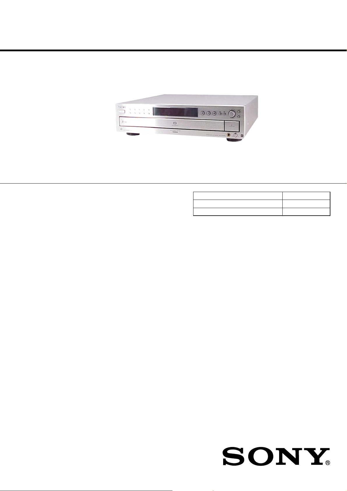
SCD-C2000ES
SERVICE MANUAL
Ver. 1.2 2005.10
SPECIFICATIONS
US Model
Canadian Model
Model Name Using Similar Mechanism SCD-CE595
CD Mechanism Type CDM79C-DVBU51
Optical Pick-up Name DBU-3
When a Super Audio CD is played
Playing frequency range 2 Hz to 100 kHz
Frequency response 2 Hz to 40 kHz (–3 dB)
Dynamic range 101 dB or more
Total harmonic distortion rate
0.003 % or less
Wow and flutter Value of measurable limit
(±0.001 % W. PEAK) or
less
When a CD is played
Frequency response 2 Hz to 20 kHz
Dynamic range 97 dB or more
Total harmonic distortion rate
0.0032 % or less
Wow and flutter Value of measurable limit
(±0.001 % W. PEAK) or
less
Output connector
ANALOG OUT (phono jacks):
Output level 2 Vrms (at 50 kilohms)
Load impedance Over 10 kilohms
DIGITAL (CD) OUT OPTICAL*
(square optical output conne c tor) :
Output level –18 dBm
DIGITAL (CD) OUT COAXIAL*
(coaxial output connector):
Output level 0.5 Vp-p
Load impedance 75 ohms
PHONES (stereo phone jack):
Output level 10 mW
Load impedance 32 ohms
*Output only the audio signals of the CD
General
Laser Semiconductor laser
(Super Audio CD: λ = 650
nm) (CD: λ = 780 nm)
Emission duration:
continuous
Power requirements 120 V AC, 60 Hz
Power consumption 15 W
Dimensions (w/h/d) 430 × 115 × 420 mm incl .
projecting parts
Mass (approx.) 5.8 kg
Supplied accessories
Audio connecting cord Red and White × 2 (2)
Black × 2 (2)
Remote commander RM-SC505 (1)
Battery R6 (size-AA) (2)
Design and specifications are subject to change
without notice.
9-879-094-03
2005J16-1
© 2005.10
SUPER AUDIO CD PLAYER
Sony Corporation
Home Audio Division
Published by Sony Engineering Corporation

SCD-C2000ES
TABLE OF CONTENTS
1. SERVICING NOTES ................................................ 3
2. GENERAL ................................................................... 4
3. DISASSEMBLY
3-1. Disassembly Flow ........................................................... 7
3-2. Upper Case ...................................................................... 8
3-3. Loading Panel.................................................................. 8
3-4. Front Panel Section ......................................................... 9
3-5. CD Mechanism Deck (CDM79C-DVBU51) .................. 9
3-6. KEY Board, LED Board, DISPLAY Board .................... 10
3-7. T able Assy ....................................................................... 10
3-8. SE-130 Board, Td Unit Assy........................................... 11
3-9. DC Motor (M901) ........................................................... 11
3-10. Pick-up Unit Section ....................................................... 12
3-11. RF Board, Pick-up Unit................................................... 12
4. DIAGRAMS
4-1. Block Diagram ................................................................ 14
4-2. Printed Wiring Board — RF Section — ......................... 15
4-3. Schematic Diagram — RF Section — ........................... 16
4-4. Printed Wiring Board — MAIN Section — ................... 17
4-5. Schematic Diagram — MAIN Section (1/4) — ............ 18
4-6. Schematic Diagram — MAIN Section (2/4) — ............ 19
4-7. Schematic Diagram — MAIN Section (3/4) — ............ 20
4-8. Schematic Diagram — MAIN Section (4/4) — ............ 21
4-9. Printed Wiring Board — DISPLAY Section — ............ 22
4-10. Schematic Diagram — DISPLAY Section —................23
4-11. Printed Wiring Board — MD-94 Board Section — ...... 24
4-12. Schematic Diagram — MD-94 Board Section — ......... 25
5. TEST MODE ............................................................... 28
NOTES ON HANDLING THE OPTICAL PICK-UP
BLOCK OR BASE UNIT
The laser diode in the optical pick-up block may suffer electrostatic
break-down because of the potential difference generated by the
charged electrostatic load, etc. on clothing and the human body.
During repair, pay attention to electrostatic break-down and also
use the procedure in the printed matter which is included in the
repair parts.
The flexible board is easily damaged and should be handled with
care.
NOTES ON LASER DIODE EMISSION CHECK
The laser beam on this model is concentrated so as to be focused on
the disc reflective surface by the objective lens in the optical pickup block. Therefore, when checking the laser diode emission,
observe from more than 30 cm away from the objective lens.
CAUTION
Use of controls or adjustments or performance of procedures
other than those specified herein may result in hazardous radiation
exposure.
LASER DIODE AND FOCUS SEARCH OPERATION
CHECK
Carry out the “S curve check” in “CD section adjustment” and check
that the S curve waveform is output three times.
Notes on chip component replacement
• Never reuse a disconnected chip component.
• Notice that the minus side of a tantalum capacitor may be
damaged by heat.
6. EXPLODED VIEWS
6-1. Main Section.................................................................... 29
6-2. Front Panel Section ......................................................... 30
6-3. Chassis Section................................................................ 31
6-4. CD Mechanism Section (1) (CDM79C-DVBU51) ......... 32
6-5. CD Mechanism Section (2) (CDM79C-DVBU51) ......... 33
7. ELECTRICAL PARTS LIST................................ 34
SAFETY-RELATED COMPONENT WARNING!!
COMPONENTS IDENTIFIED BY MARK 0 OR DOTTED LINE
WITH MARK 0 ON THE SCHEMATIC DIAGRAMS AND IN
THE PARTS LIST ARE CRITICAL TO SAFE OPERATION.
REPLACE THESE COMPONENTS WITH SONY PARTS WHOSE
PART NUMBERS APPEAR AS SHOWN IN THIS MANUAL OR
IN SUPPLEMENTS PUBLISHED BY SONY.
Flexible Circuit Board Repairing
• Keep the temperature of the soldering iron around 270 °C
during repairing.
• Do not touch the soldering iron on the same conductor of the
circuit board (within 3 times).
• Be careful not to apply force on the conductor when soldering
or unsoldering.
ATTENTION AU COMPOSANT AYANT RAPPORT
À LA SÉCURITÉ!
LES COMPOSANTS IDENTIFIÉS PAR UNE MARQUE 0 SUR
LES DIAGRAMMES SCHÉMATIQUES ET LA LISTE DES
PIÈCES SONT CRITIQUES POUR LA SÉCURITÉ DE
FONCTIONNEMENT. NE REMPLACER CES COM- POSANTS
QUE PAR DES PIÈCES SONY DONT LES NUMÉROS SONT
DONNÉS DANS CE MANUEL OU DANS LES SUPPLÉMENTS
PUBLIÉS PAR SONY.
2

SECTION 1
tapering driver
1
2
r
SERVICING NOTES
SCD-C2000ES
SAFETY CHECK-OUT
After correcting the original service problem, perform the following
safety check before releasing the set to the customer:
Check the antenna terminals, metal trim, “metallized” knobs, screws,
and all other exposed metal parts for AC leakage.
Check leakage as described below.
LEAKAGE TEST
The AC leaka ge from any exposed metal part to earth ground and
from all exposed metal parts to any exposed metal part having a
return to chassis, must not exceed 0.5 mA (500 microamperes.).
Leakage current can be measured by any one of three methods.
1. A commercial leakage tester, such as the Simpson 229 or RCA
WT -540A. Follow the manufactur ers’ instructions to use these
instruments.
2. A battery-operated AC milliammeter. The Data Precision 245
digital multimeter is suitable for this job.
3. Measuring the voltage drop across a resistor by means of a
VOM or battery-operated AC v oltmeter. The “limit” indication
is 0.75 V, so analog meters must have an accurate low-v oltage
scale. The Simpson 250 and Sanwa SH-63Trd are examples
of a passive VOM that is suitable. Nearly all battery operated
digital multimeters that have a 2 V A C range are suitable. (See
Fig. A)
To Exposed Metal
Parts on Set
HOW TO OPEN THE DISC TRAY WHEN POWER
SWITCH TURNS OFF
Insert a tapering driver into the aperture of the unit bottom, and turn
in the direction of arrow.
Use a flat (-) head screwdriver to open the disc tray by manual
operation. (Flat head screwdriver with nominal blade length of
3mm.)
* To close the disc table, turn the driver in the reverse direction.
AC
0.15 µF
1.5 k
Ω
Earth Ground
voltmete
(0.75 V)
Fig. A. Using an AC voltmeter to check AC leakage.
3
SCD-C2000ES
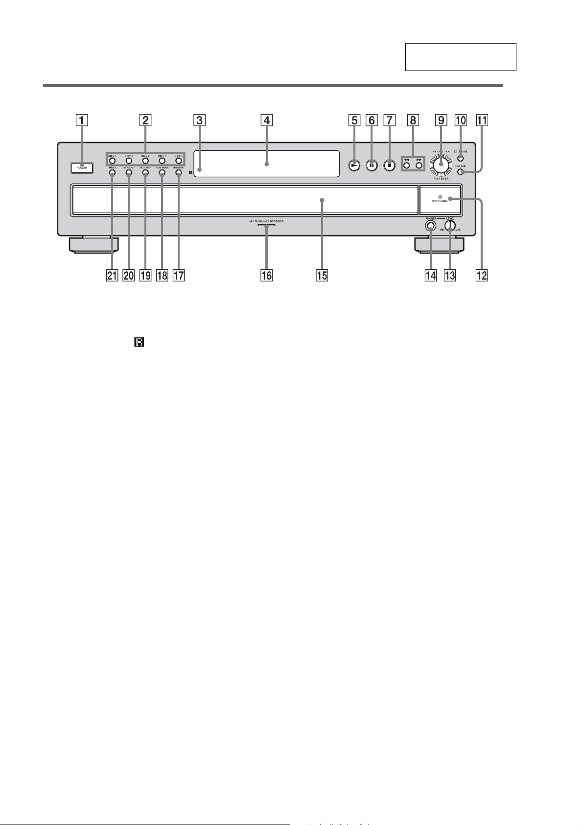
Front Panel
SECTION 2
GENERAL
This section is extracted
from instruction manual.
A POWER swit ch (9, 22)
B DISC 1-5 buttons (10, 15)
Press to select the disc directly.
C Remote sensor (6)
D Display window (11)
E N button (10, 14, 15)
F X button (10)
G x button (10, 16, 22)
H m/M buttons (1 4 , 21 )
I l AMS L dial
(AMS: Automatic Music Sensor) (9, 10, 13,
14, 15, 17, 18, 20, 21)
J EX-CHANGE button (13)
Press to replace disc s whil e playing a disc.
K DISC SKIP button (9, 13)
Press to select the disc.
L A OPEN/CLOSE button (9)
M LEVEL control
Adjust the headphones volum e.
N PHONES jack
Connect the headphones.
During playback of a Multi-chann el Sup er Audi o
CD, the same signal that is output from the
ANALOG 5.1CH OUT FRONT L/R jacks is
output from the PHON ES ja c k.
O Disc tray (9)
P MULTI CHANNEL DECODING indicator
Turns on when you turn on the player, or when the
Multi-channel Super Audio CD is loa ded and
select the m ulti-c hanne l play back area by pr essin g
MULTI/2CH.
Q TIME/TEXT button (12)
Each time you press the button, the playing time of
the track, the remaining time of the disc, or TEXT
information appears in the display.
In name input mode, pr ess to select the char acter
type.
R PLAY MODE button (9, 15)
Press to select the play mode.
S MULTI/2CH button (5, 10)
Press to select the playback area when a disc with
the 2 channel area and the multi-c ha nnel area is
loaded.
T SA-CD/CD button (5, 10)
Each time you press the button while playing back
a hybrid disc, the layer to be played back switches
between the SA-CD la ye r and the CD layer.
U MENU button (9, 10, 13, 17, 1 8, 20, 21)
Press to enter the menu .
Press to exit from th e menu and return to the
normal display.
4
SCD-C2000ES
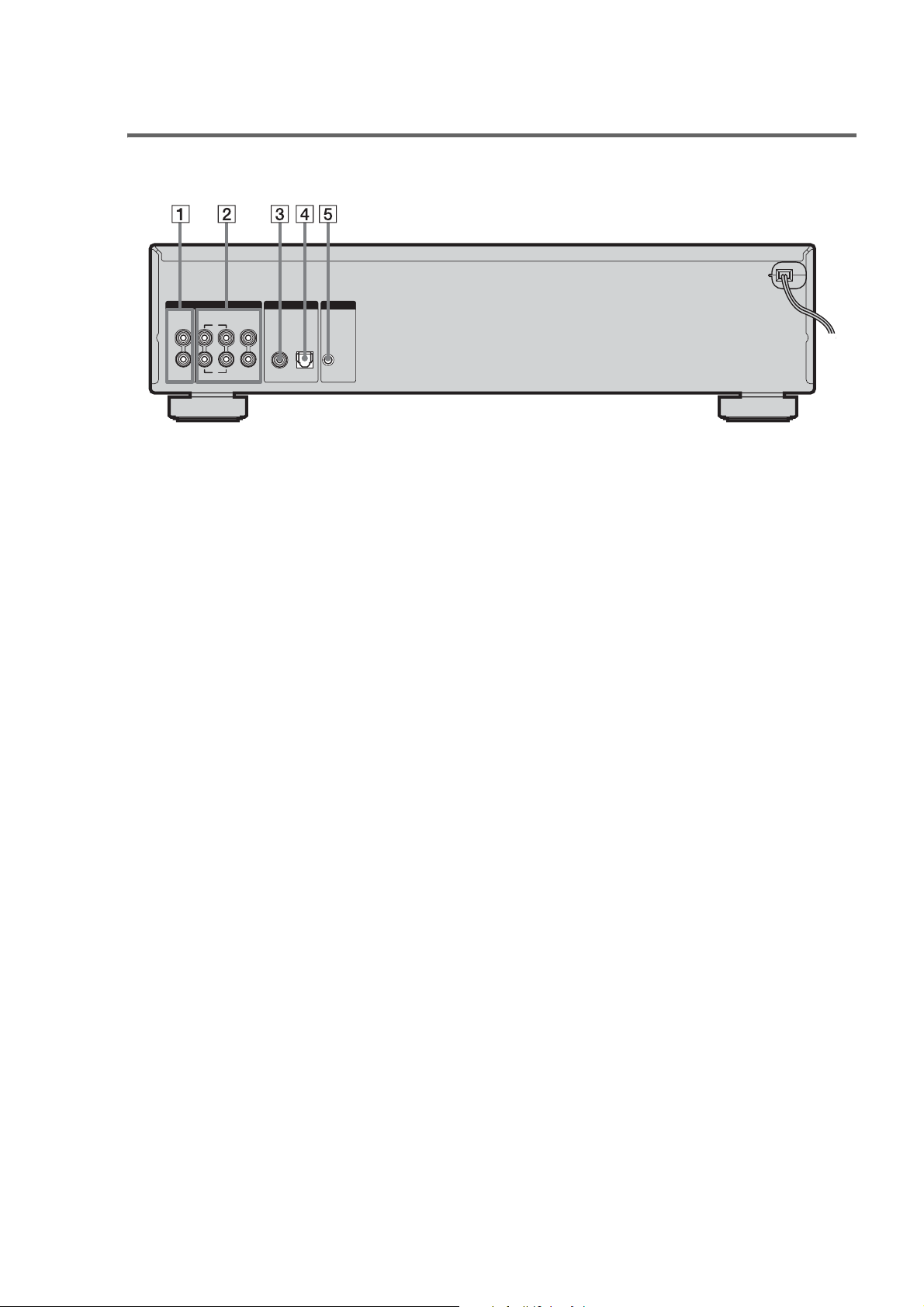
Rear Panel
A ANALOG 2CH OUT jacks (7)
B ANALOG 5.1CH OUT jacks (6)
C DIGITAL (CD) OUT COAXIAL connector (8)
D DIGITAL (CD) OUT OPTICAL connector (8)
E IR REMOTE IR IN jack
Connect to a component equipped with the IR
output jack.
5.1CH OUT2CH OUT
OPTICALCOAXIAL
SURR
L
L
R
R
CENTER
SUB
WOOFER
FRONT
OUT
ANALOG DIGITAL(CD) IR REMOTE
IR
IN
5
SCD-C2000ES
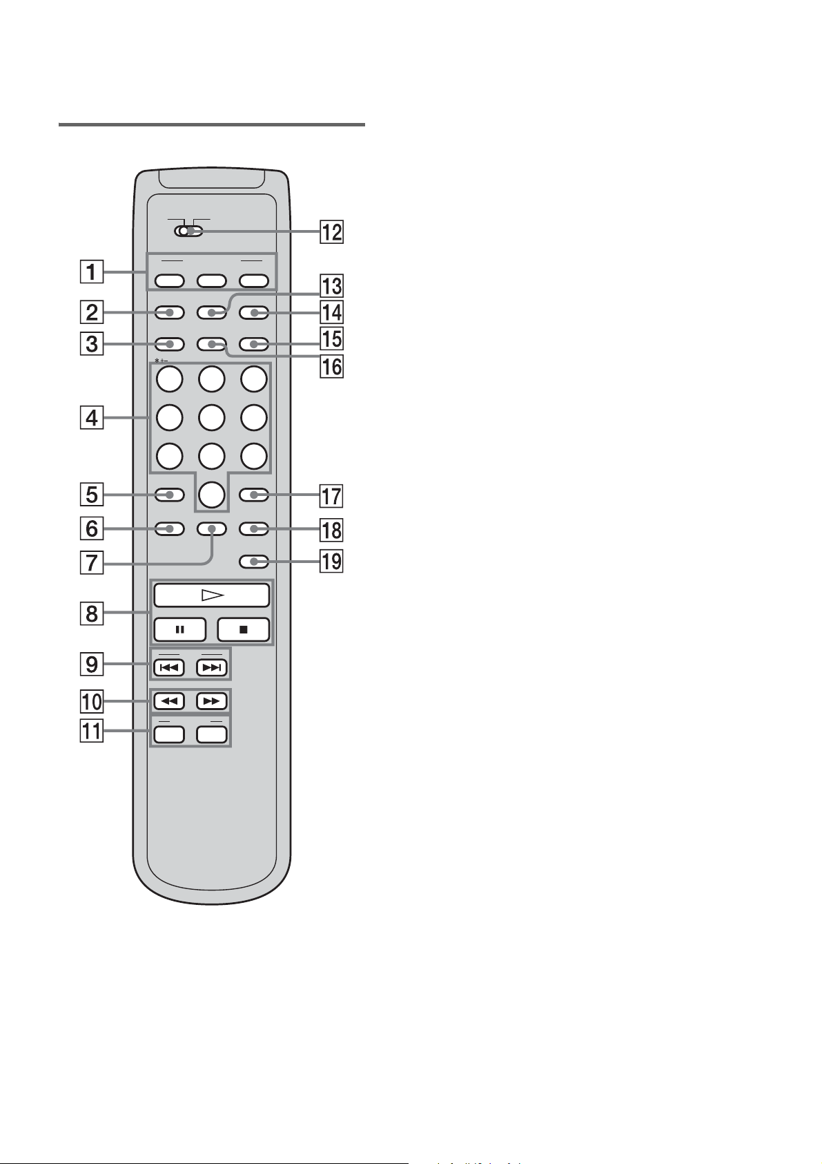
Remote
CD2
CD1
PLAY MODE
CONTINUE SHUFFLE
NAME
INPUT
TIME/TEXT
DISC
CAPS
PROGRAM
DISPLAY
SA-CD/CD
MODE
MULTI/2CH
SPACE
ABC DEF
123
JKL MNOGHI
456
TUV WXYZPQRS
78
>10 ENTER
10/0
REPEAT CHECK
AMS
DISC SKIP
–+
9
CLEAR
LEVEL
ADJ
A CONTINUE button (9, 15, 16)
Press to resume Continuous Play from Shuffle Play
or Program Play.
SHUFFLE button (15)
PROGRAM button (15)
B NAME INPUT button (21)
Press to enter the nam e in put mode.
C DISC button (10, 15)
Press to select the disc .
CAPS button (21)
Press to switch be tween capital lett ers (ABC) and
numbers (123) in name input mode.
D Numeric buttons (10, 15, 21 )
E >10 button (10, 15)
F REPEAT button (14)
G CHECK button (16)
Press to check the programed order.
H H button (10, 14, 15)
X button (10)
x button (10, 16, 22)
I AMS ./> buttons
(AMS: Automatic Music Sensor) (9, 10, 13,
14, 15, 17, 18, 20, 21)
J m/M buttons (14, 21)
K DISC SKIP +/– buttons (9, 13)
Press to select the disc .
L CD1/2 (command mode) switch (9)
Select the command mod e .
M DISPLAY MODE button (13)
Press to turn the displa y information o ff or o n.
N SA-CD/CD button (5, 10)
Each time you press the button while playing back
a hybrid disc, the layer to be played back switches
between the SA-CD la ye r and the CD layer.
O MULTI/2CH button (5, 10)
Press to select the playback area when a disc with
the 2 channel area and the multi-c ha nnel area is
lo aded.
P TIME/TEXT button (12)
Each time you press the button, the playing time of
the track, the remaining time of the disc, or TEXT
information appears in the display.
SPACE button (21)
Press to insert a space in name input mode.
Q ENTER button (9, 10, 13, 15, 17, 19, 2 0, 22)
R CLEAR button (15, 16, 22)
Press to delete a programe d tr a c k n umber.
S LEVEL ADJ button (18)
Press to adjust the output level balance for the
Multi-channel management function.
6
•This set can be disassembled in the order shown below.
•The dotted square with arrow (
) prompts you to move to the next job when all of the works within the dotted square ( ) are
completed.
3-1. DISASSEMBLY FLOW
SET
SCD-C2000ES
SECTION 3
DISASSEMBLY
3-2. UPPER CASE
(Page 8)
3-4.FRONT PANEL SECTION
(Page 9)
3-5.CD MECHANISM DECK
(CDM79C-DVBU51)
(Page 9)
3-7.TABLE ASSY
(Page 10)
3-8.SE-130 BOARD, TD UNIT ASSY
(Page 11)
3-3. LOADING PANEL
(Page 8)
3-6.KEY BOARD, LED BOARD,
DISPLAY BOARD
(Page 10)
3-9.DC MOTOR (M901)
(Page 11)
3-10.PICK-UP UNIT SECTION
(Page 12)
3-11.RF BOARD, PICK-UP UNIT
(Page 12)
7
SCD-C2000ES
s
r
Note: Follow the disassembly procedure in the numerical order given.
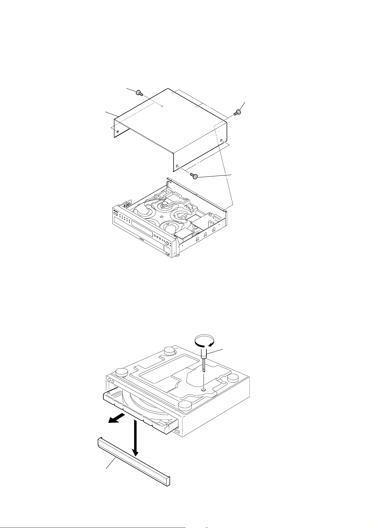
3-2. UPPER CASE
1
two screws
(BV/RING)
4
upper case
2
3
two screws
(BV/RING)
three screw
(BV/RING)
3-3. LOADING PANEL
2
loading panel
3
1
tapering drive
8

)
3-4. FRONT PANEL SECTION
)
4
connector
(2p) (CN891)
8
three screws
(+BVTP 3
9
front panel section
×
7
four screws
(+BVTP 3
8)
1
×
5
screw
(+BVTP 2.6
connector
(2p) (CN101)
8)
SCD-C2000ES
×
8)
3
wire (flat type)
(13 core) (CN703
6
screw
2
connector
(3p) (CN881)
(+BVTP 2.6
×
8)
3-5. CD MECHANISM DECK
(CDM79C-DVBU51)
8
9
CD mechanism deck
(CDM79C-DVBU51)
two screws
(+BVTP 3
gear (shaft)
4
7
×
8)
two screws
(+BVTP 3
5
wire (flat type)
(31 core) (CN702
6
connector
(11p) (CN001)
×
8)
2
sub shassis
1
3
Turn the gear (shaft) in the
direction of the arrow.
three screws
(+BVTP 3
×
8)
9

SCD-C2000ES
)
3-6. KEY BOARD, LED BOARD, DISPLAY BOARD
q;
claw
qa
DISPLAY board
9
connector
(2p) (CN804)
5
connector
(2p) (CN814)
8
6
LED board
connector
(3p) (CN805)
2
connector
(3p) (CN813)
7
3
nine screws
(+BVTP 2.6
4
two screws
(+BVTP 2.6
KEY board
×
8)
×
8)
1
four screws
(+BVTP 2.6
×
8
3-7. TABLE ASSY
4
6
plate (guide)
screw
(+BTP 2.6
5
claw
×
8)
3
7
screw
(+BTP 2.6
qa
table assy
1
floating screw
(+PTPWH M2.6)
2
tray
0
flat type wire
(6 core) (CN002)
×
8)
10
plate (guide)
9
8
claw
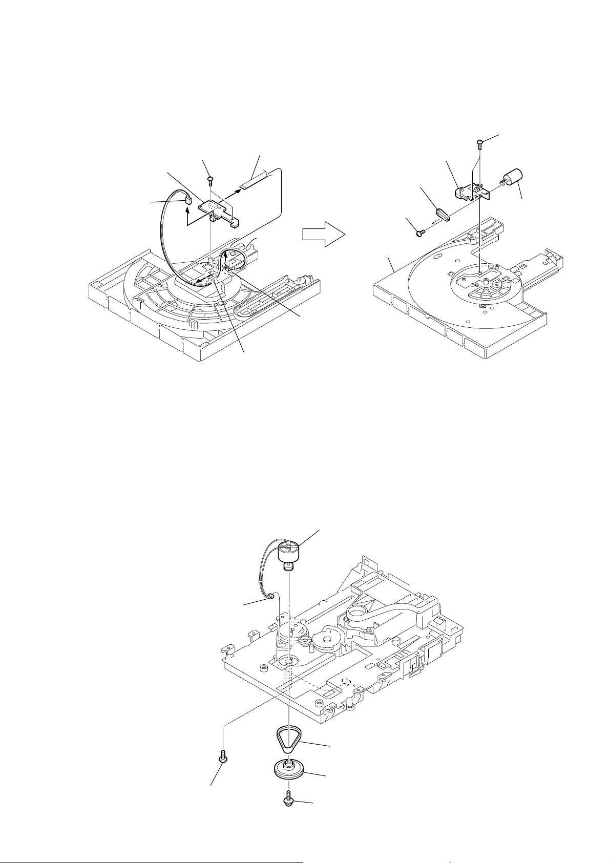
3-8. SE-130 BOARD, TD UNIT ASSY
4
two screws
(+BTP 2.6 × 8)
6
SE-130 board
1
connector
(CN102)
5
flat type wire
(6 core) (CN101)
0
8
two screws
(+P 3
table assy
qa
TD belt
×
3)
TD unit assy
SCD-C2000ES
7
two screws
(+BTP 2.6 × 8)
9
TD motor assy
3-9. DC MOTOR (M901)
5
connector
(CN004)
2
claw
3
claw
6
DC motor (M901)
4
two screws
(+P 2.6
3
belt (loading)
2
gear (loading A)
×
4)
1
screw
(+PTPWH M2.6)
11
SCD-C2000ES
y
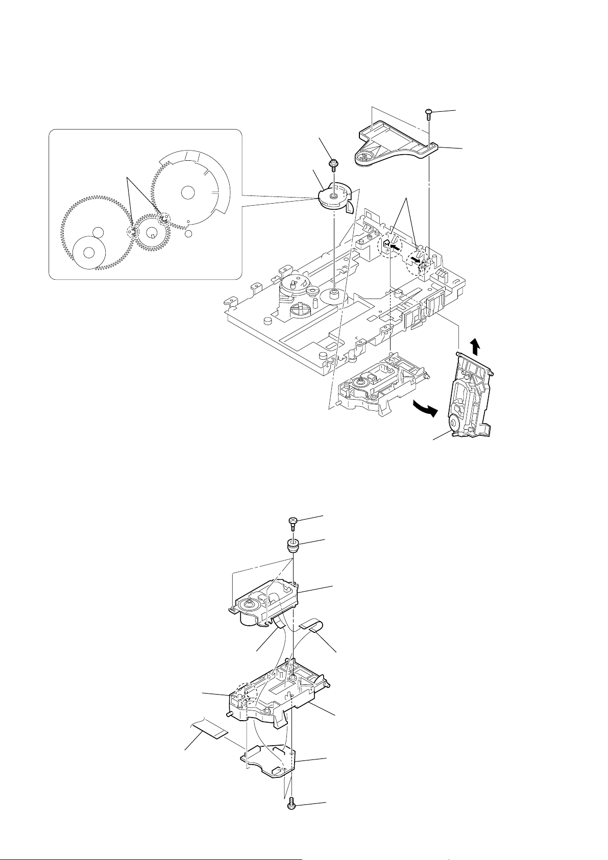
3-10. PICK-UP UNIT SECTION
PRECAUTION DURING GEAR (CHUC)
adjust phases
gear (chuck)
3
screw
(+PTPWH M2.6)
4
gear (chuck)
1
two screws
(+BV B3)
2
chuck ass
gear (loading B)
gear (idoler)
6
two claws
8
pick-up unit section
7
5
3-11. RF BOARD, PICK-UP UNIT
4
(CN003)
2
5
flexible flat cable (31 core)
(CN002)
flexible flat cable (9 core)
claw
7
three step screws (M)
8
three insulators
9
pick-up unit
3
flexible flat cable (24 core)
(CN001)
9
holder (BU) assy
6
RF board
12
1
two screws
(+BTP 2.6
×
10)
SECTION 4
DIAGRAMS
SCD-C2000ES
NOTE FOR PRINTED WIRING BOARDS AND SCHEMATIC DIAGRAMS
Note on Printed Wiring Board:
• X : parts extracted from the component side.
• Y : parts extracted from the conductor side.
• W : indicates side identified with part number.
• f : internal component.
• : Pattern from the side which enables seeing.
Caution:
Pattern face side: Parts on the pattern face side seen from
(Side B) the pattern face are indicated.
Parts face side: Parts on the parts face side seen from
(Side A) the parts face are indicated.
• Indication of transistor.
C
Q
B
E
These are omitted.
Note Schematic Diagrams.
• All capacitors are in µF unless otherwise noted. (p: pF)
50 WV or less are not indicated except f or electrolytics and
tantalums.
• All resistors are in Ω and 1/
specified.
• f : internal component.
• C : panel designation.
Note:
The components identified by mark 0 or dotted line with mark 0 are
critical for safety.
Replace only with part
number specified.
• A : B+ Line.
• B : B– Line.
•Voltages and waveforms are dc with respect to ground
under no-signal conditions.
no mark: SACD PLAY
( ) : CD PLAY
•Voltages are taken with a VOM (Input impedance 10 MΩ).
Voltage v ariations ma y be noted due to normal production
tolerances.
•Waveforms are taken with a oscilloscope.
Voltage v ariations ma y be noted due to normal production
tolerances.
• Circled numbers refer to waveforms.
• Signal path.
J : CD
c : CD DIGITAL OUT (OPTICAL)
4
W or less unless otherwise
Note:
Les composants identifiés
par une marque 0 sont critiques pour la sécurité.
Ne les remplacer que par une
piéce portant le numéro
spécifié.
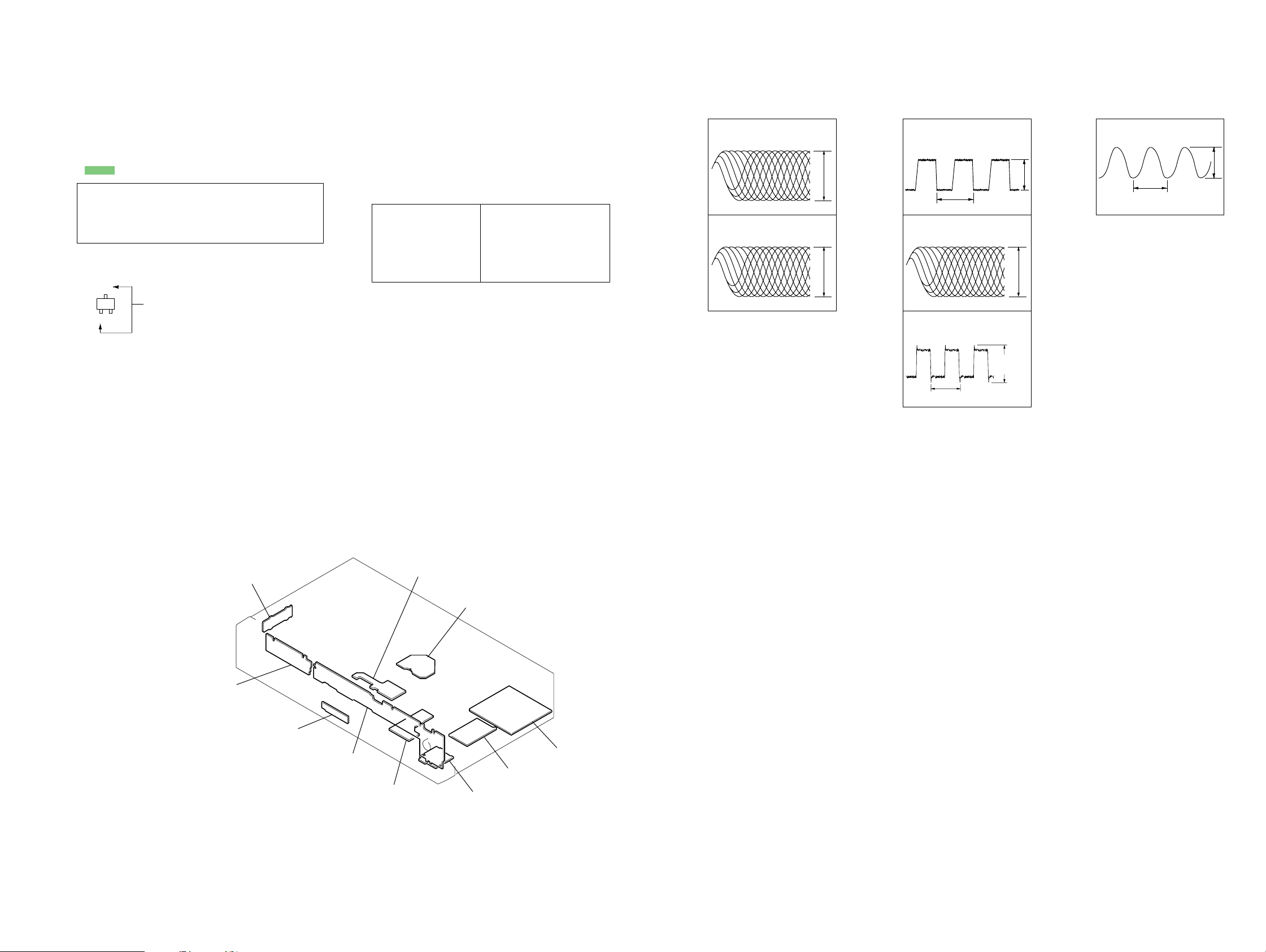
•Waveforms
– RF Board – – MAIN Board – – DISPLAY Board –
5
1
IC001 tl SIGO (CD)
200 ns/DIV
1
IC001 tl SIGO (SACD)
40 ns/DIV
1.4 Vp-p
1.4 Vp-p
2
IC706 uk DSPHREFO
354 ns
3
4
<z./
IC706
40 ns/DIV
RF IN (SACD)
1.4 Vp-p
IC320 2,4,6,q;,qs
88.6 ns
3.3 to 3.5
Vp-p
3.3 to 3.5
Vp-p
IC801 3 X1
200 ns
3.1 Vp-p
1 V/DIV, 200 ns/DIV
• Circuit Boards Location
KEY board
POWER SW board
LED board
DISPLAY board
MD-94 board
SE-130 board
RF board
MAIN board
PT board
HP board
SCD-C2000ES
1313

SCD-C2000ES
4-1. BLOCK DIAGRAM
TURN TABLE
MOTOR
PH101
PH102
IC309(1/2)
HEADPHONE AMP
611
BUFFER
Q341
+3.3V
IC950
+5V REG
IC985
AU+ REG
D OUT
MUTE
OPTICAL PICK-UP BLOCK
IC001
19
VC
1
RFIP
14
A
13
B
12
C
11
D
15
E
16
F
25
DVDLD
26
CDLD
24
LDSELO
2
PD
MOTOR/COIL DRIVER
37
DO1+
36
DO1-
35
DO2+
34
DO2-
32
DO3+
31
DO3-
30
DO4+
29
DO4-
28
DO5+
27
DO5-
46
OPIN1-
47
OPIN1+
25
DO6+
24
DO6-
Q822-Q825
FLDRIVER
Q823
Q822
RF AMP
41TE
42FE
PI
36
33MIRR
TZC
37
DFT
38
45SRD 245
46SWD 246
47SCLK 247
48SDEN 244
LDON
27
VCI
39
IC712
IN1+
48
IN1-
1
IN2+
3
4
IN2-
5
OUT2
IN3+
6
IN3-
7 SLDB
9
IN4+
IN4-
10 SLDA
12
IN5+
IN5-
13
45
OPOUT1
1716REV
FWD
PS
39
MUTE12
19
MUTE34
20
MUTE5
21
Q825
Q824
+3.3V
FLDRIVER
Q821
LIMIT
IN
SWITCH
D509
S841-845,
S851-853,855,
S875-871
IC802
SIRCS
VCC
VC
RF
A
B
C
D
E
F
DVDLD
CDLD
SW
PD
VR
GND
FCS+
FCS-
TR+
TR-
M
M
M
SPM+
LOADP
M
LOADN
INDICATION TUBE
FL801
SLB+
SLB-
SLA+
SLA-
SPM-
A5V
Q001
LD
DRIVE
Q002
LD
DRIVE
5
6
7
8
9-20,32-48
49
6,14
5
3
8
9
2
1
7
10
17
19
15
12
4
FOCUS
COIL
TRACKING
COIL
SLED B
MOTOR
SLED A
MOTOR
SPINDLE
MOTOR
LOADING
MOTOR
M
4
3
2
1
2
3
4
TM-
TM+
DSENS
SENSOR
TSENS
1
1
LED
IC706
DIGITAL SERVO,
DIGITAL SIGNAL PROCESSOR
DOUT958
19059SIGO
RFAC
PCMD1
200
201
202
231
230
229
234 INLIM
215
216
213
214
203
220
219
206
221
222
204
235
RM
CDBCK
TEI
CDLRCK
FEI
DSAL
PI
DSAR
DSALS
MIRR
DSARS
TZC
DSAC
DFCTI
DSASW
DSPHREFO
SSI
MCKI
SSO
29
+3.3V
SCK
SCS
FDOP
FDON
TDOP
TDON
SEI
VCO
MDS0
MDP0
SP RV
FGMODE
1
21-29 13,15-22A0-8 CA0-8
11-18 4-11D0-7 CD0-7
XINT
XCS
XWAIT
XWR
XRD
XRST
JIT
SMUTE
MA0-10,BA A0-10,BA
MD0-15 DQ0-15
XRAS,
XCAS,
XMWR,
MCKE,
MMCK,
LDQM,
UDQM
X801
5MHz
KEY
100
226
96
95
94
83
84
85
86
89
90
78
3
32
33
34
35
36
37
61
4
12
16
7
DISPLAY CONTROLLER
3X1
4X2
17 SIRCS
22-19
ANI0-3
80 FIP0
79 FIP1
78 FIP2
77 FIP3
76-61,58-46
45 FIP33
IC701
RESET
IC702
EEPROM
IC708
16M SDRAM
RAS,
CAS,
WE,
CKE,
CLK,
LDQM,
UDQM
IC801
FIP4-32
IC705
Q826
MASTER CONTROL
92
XINT0
87
XCS
73
XWAIT
71
XWR
70
XRD
72
XWRST
59
XRST
EPR/B,
XEPCS,
XEWC,
EEPSO,
EEPSI,
EEPSCK
52
JIT
74
SMUTE
38
XLDON
TRAY OUT33
TRAY IN
30
DRV ON
35
36
SP ON
849 IFSISO1
838 IFSOSI1
9112 XIFINTACK
857 IFSCSCK1
9615 XIFCSINTP0
3SLATR DAC
2SCLK DAC
1SDATA DAC
94MZR
95MZL
L MUTE
98
97R MUTE
100M/2
S001 (TRY POSITION DETECT SWITCH)
25LOAD S0
27LOAD S1
26LOAD S2
39TRMP
40TRMM 2OUT2
29DSENS
30TSENS TSENS
EXTAL
65
ROTARY
ENCODER
IC710
TURN TABULE MOTOR DRIVER
9
RIN
7
FIN
INVERTER
Q701
+1.8V
4OUT1
TM-
TM+
DSENS
SENSOR
LED
3.3V
X321
11.2896MHz
56
34
11 10
13 12
9812
IC320
INVERTER
IC703
+1.8V REG
3 1
+5V
AU+
1
3 1
3 1
9
8
D511
6
OUT
6RESET
D801
LED DRIVER
11P23
J341
IC330
OPTICAL OUT
1
IC920
+3.3V REG
3 1
MUTE REG
Q961
COAXIAL
OPTICAL
D961,965
+12V
RECT
DIGITAL
OUT
(CD)
IC200
DAC
4
PDATA
3 PBCK
5 PLRCK
1 DSDL
2 DSDR
20 DBCK
19 DSCK
18 PSCK
17 MS
16 MC
15 MD
14 ZEROR
13 ZEROL
IC230
DAC
3 PBCK
5 PLRCK
1 DSDL
2 DSDR
20 DBCK
19 DSCK
18 PSCK
17 MS
16 MC
15 MD
IC260
DAC
3 PBCK
5 PLRCK
1 DSDL
2 DSDR
20 DBCK
19 DSCK
18 PSCK
17 MS
16 MC
15 MD
VFL
D921-924
D931-934
RECT
D936,981,983,984
VOUTL
VOUTR
VOUTL 9
VOUTR
VOUTL
VOUTR
VFL REG
Q971
RECT
RECT
9
10
SL
SR
10
CENTER
9
SW
10
VF2
VF1
IC309(2/2)
HEADPHONE AMP
IC400(1/2)
IC400(2/2)
IC430(1/2)
IC430(2/2)
IC460(1/2)
IC460(2/2)
POWER TRANSFORMER
SUB POWER TRANSFORMER
21
AMP
67
Q401,402
AMP
21
Q501,502
AMP
67
Q431,432
AMP
21
Q531,532
AMP
67
Q462,463
AMP
21
Q562,563
T101
D971
T102
HP MUTE
HP MUTE
MUTE
MUTE
L MUTE
Q303
R MUTE
Q305
MUTE
Q301
MUTE
MUTE
MUTE
MUTE
Q403
Q503
RV881
LEVEL
S891
POWER
J352
J351(1/3)
J351(2/3)
J351(3/3)
L
R
L
R
SL
SR
CENTER
SW
J881
PHONES
2CH OUT
• Signal Path
: CD
: CD DIGITAL OUT (OPTICAL)
SCD-C2000ES
IR CONTROL
1
COM
7
CH0
IC803
6CH1
MUTE
Q806
J701
IR IN
1414
 Loading...