

( )
When a super audio CD is played
Playing frequency range 2 Hz to 100 kHz
Frequency response 2 Hz to 50 kHz (–3 dB)
Dynamic range 105 dB or more
Total harmonic distortion rate
0.0012 % or less
Wow and flutter Value of measurable limit (±0.001 %
W. PEAK) or less
When a CD is played
Frequency response 2 Hz to 20 kHz
Dynamic range 100 dB or more
Total harmonic distortion rate
0.0017 % or less
Wow and flutter Value of measurable limit (±0.001 %
W. PEAK) or less
Output connector
*Output only the audio signals of the CD
General
Laser radiant power: 5.47 uW at 650 nm
*These output is the value measured at a distance of about
200mm from the objective lens surface on the optical pick-up.
Power requirements 230 V AC, 50/60 Hz
Power consumption 26 W
Dimensions (w/h/d) 430 × 130 × 380 mm incl. projecting
parts
Mass (approx.) 14.5 kg
Supplied accessories
Design and specifications are subject to change without notice.
Load impedance
ANALOG OUT
DIGITAL (CD)
OUT OPTICAL*
DIGITAL (CD)
OUT COAXIAL*
Phono
jacks
Jack type
2 Vrms
(at 50 kilohms)
Square
optical
output
connector
–18 dBm
0.5 Vp-p
Over 10 kilohms
Light emitting
wave length:
660 nm
Output level
75 ohms
Coaxial
output
connector
PHONES
Stereo
phone jack
32 ohms
20 mW
•Audio connecting cord
(phono jack × 2 y phono jack × 2) (1)
•Mains lead (1)
•Remote commander (remote) RM-SX90 (1)
•R06 (size-AA) batteries (2)
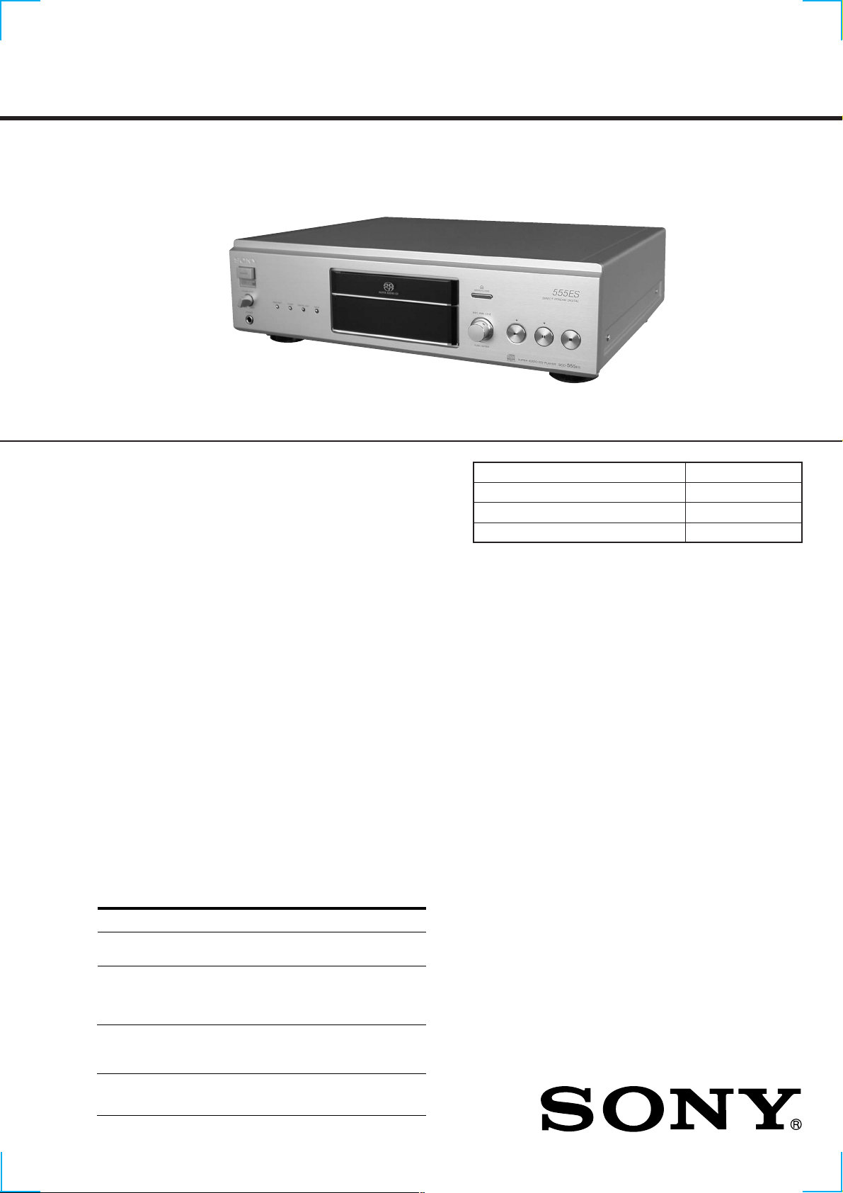
SCD-555ES
SERVICE MANUAL
Photo: Gold type
SPECIFICATIONS
AEP Model
Model Name Using Similar Mechanism CDP-D500
CD Mechanism Type CDM19HN-DVBU4
Base Unit Name DVBU4
Optical Pick-up Name KHM-230AAA/J1NP
SUPER AUDIO CD PLAYER
TABLE OF CONTENTS
1. SERVICING NOTES (1) ........................................ 3
2. GENERAL ................................................................... 6
CAUTION
Use of controls or adjustments or performance of procedures
other than those specified herein may result in hazardous radiation exposure.
3. DISASSEMBLY ......................................................... 9
4. DIAGRAMS
4-1. Notes for Printed Wiring Boards and
Schematic Diagrams ....................................................... 15
4-2. Printed Wiring Boards
– RF/SWITCH/LOADING MOTOR Boards – .............. 16
4-3. Schematic Diagram
– RF/SWITCH/LOADING MOTOR Boards – .............. 17
4-4. Printed Wiring Board
– MAIN Board (Component Side) – .............................. 18
4-5. Printed Wiring Board
– MAIN Board (Conductor Side) – ................................ 19
4-6. Schematic Diagram – MAIN Board (1/6) – .................. 20
4-7. Schematic Diagram – MAIN Board (2/6) – .................. 21
4-8. Schematic Diagram – MAIN Board (3/6) – .................. 22
4-9. Schematic Diagram – MAIN Board (4/6) – .................. 23
4-10. Schematic Diagram – MAIN Board (5/6) – .................. 24
4-11. Schematic Diagram – MAIN Board (6/6) – .................. 25
4-12. Printed Wiring Board
– AUDIO Board (Component Side) – ............................ 26
4-13. Printed Wiring Boards – AUDIO (Conductor Side)/
LINE OUT/HEADPHONE Boards – ............................. 27
4-14. Schematic Diagram – AUDIO Board (1/2) – ................ 28
4-15. Schematic Diagram – AUDIO (2/2)/LINE OUT/
HEADPHONE Boards – ................................................. 29
4-16. Printed Wiring Board – DIGITAL OUT Board –.......... 30
4-17. Schematic Diagram – DIGITAL OUT Board – ............ 31
4-18. Printed Wiring Board – DISPLAY Board – .................. 32
4-19. Schematic Diagram – DISPLAY Board – ..................... 33
4-20. Printed Wiring Boards
– JOG/KEY/R. CNTL Boards – ..................................... 34
4-21. Schematic Diagram – JOG/KEY/R. CNTL Boards – ... 34
4-22. Schematic Diagram
– POWER/AC/POWER SWITCH Boards – .................. 35
4-23. Printed Wiring Board
– POWER Board (Component Side) – ........................... 36
4-24. Printed Wiring Boards – POWER (Conductor Side)/
AC/POWER SWITCH Boards – .................................... 37
4-25. IC Pin Function Description ........................................... 47
This appliance is classified as a CLASS 1
LASER product.
The CLASS 1 LASER PRODUCT
MARKING is located on the rear exterior.
The following caution label is located
inside the unit.
Notes on chip component replacement
• Never reuse a disconnected chip component.
• Notice that the minus side of a tantalum capacitor may be damaged by heat.
Flexible Circuit Board Repairing
• Keep the temperature of the soldering iron around 270 ˚C during repairing.
• Do not touch the soldering iron on the same conductor of the
circuit board (within 3 times).
• Be careful not to apply force on the conductor when soldering
or unsoldering.
5. SERVICING NOTES (2) ........................................ 59
6. TEST MODE ............................................................... 60
7. EXPLODED VIEWS................................................ 74
8. ELECTRICAL PARTS LIST ............................... 80
2
SAFETY-RELATED COMPONENT WARNING!!
COMPONENTS IDENTIFIED BY MARK 0 OR DOTTED
LINE WITH MARK 0 ON THE SCHEMATIC DIA GRAMS
AND IN THE PARTS LIST ARE CRITICAL TO SAFE
OPERATION. REPLACE THESE COMPONENTS WITH
SONY PARTS WHOSE PART NUMBERS APPEAR AS
SHOWN IN THIS MANUAL OR IN SUPPLEMENTS PUBLISHED BY SONY.
SECTION 1
e
SERVICING NOTES (1)
NOTES ON HANDLING THE OPTICAL PICK-UP
BLOCK OR BASE UNIT
The laser diode in the optical pick-up block may suffer electrostatic break-down because of the potential difference generated
by the charged electrostatic load, etc. on clothing and the human
body.
During repair, pay attention to electrostatic break-down and also
use the procedure in the printed matter which is included in the
repair parts.
The flexible board is easily damaged and should be handled with
care.
NOTES ON LASER DIODE EMISSION CHECK
The laser beam on this model is concentrated so as to be focused
on the disc reflective surface by the objective lens in the optical
pick-up block. Therefore, when checking the laser diode emission, observe from more than 30 cm away from the objecti ve lens.
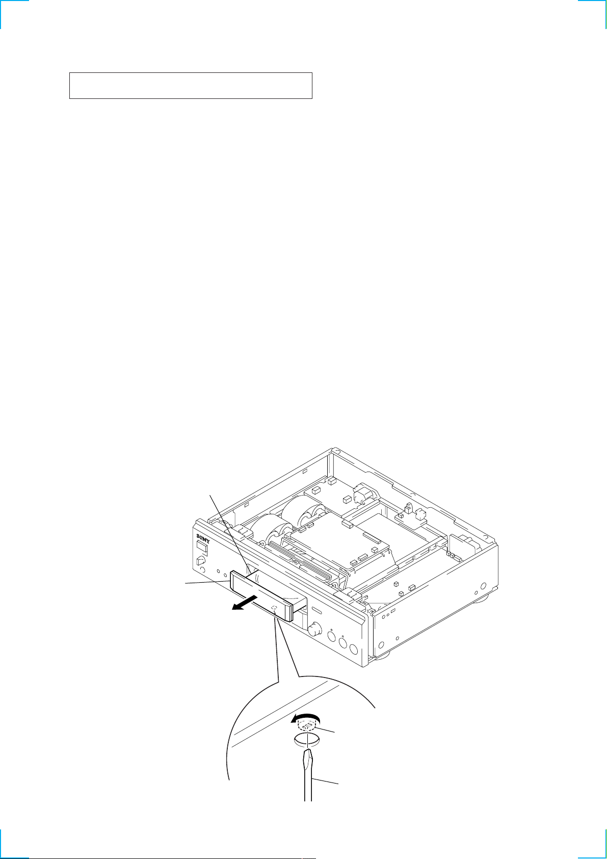
HOW TO OPEN THE DISC TABLE WHEN POWER SWITCH TURNS OFF
disc table
loading panel ass’y
B
2
Draw out the loading panel ass’y
in the direction of arrow
B
.
A
cover (CAM)
tapering driver
1
Insert a tapering driver in the hol
at the bottom of the unit,
turn the cover (CAM) fully in the
direction of arrow A.
3
Note: Follow the disassembly procedure in the numerical order given.
s
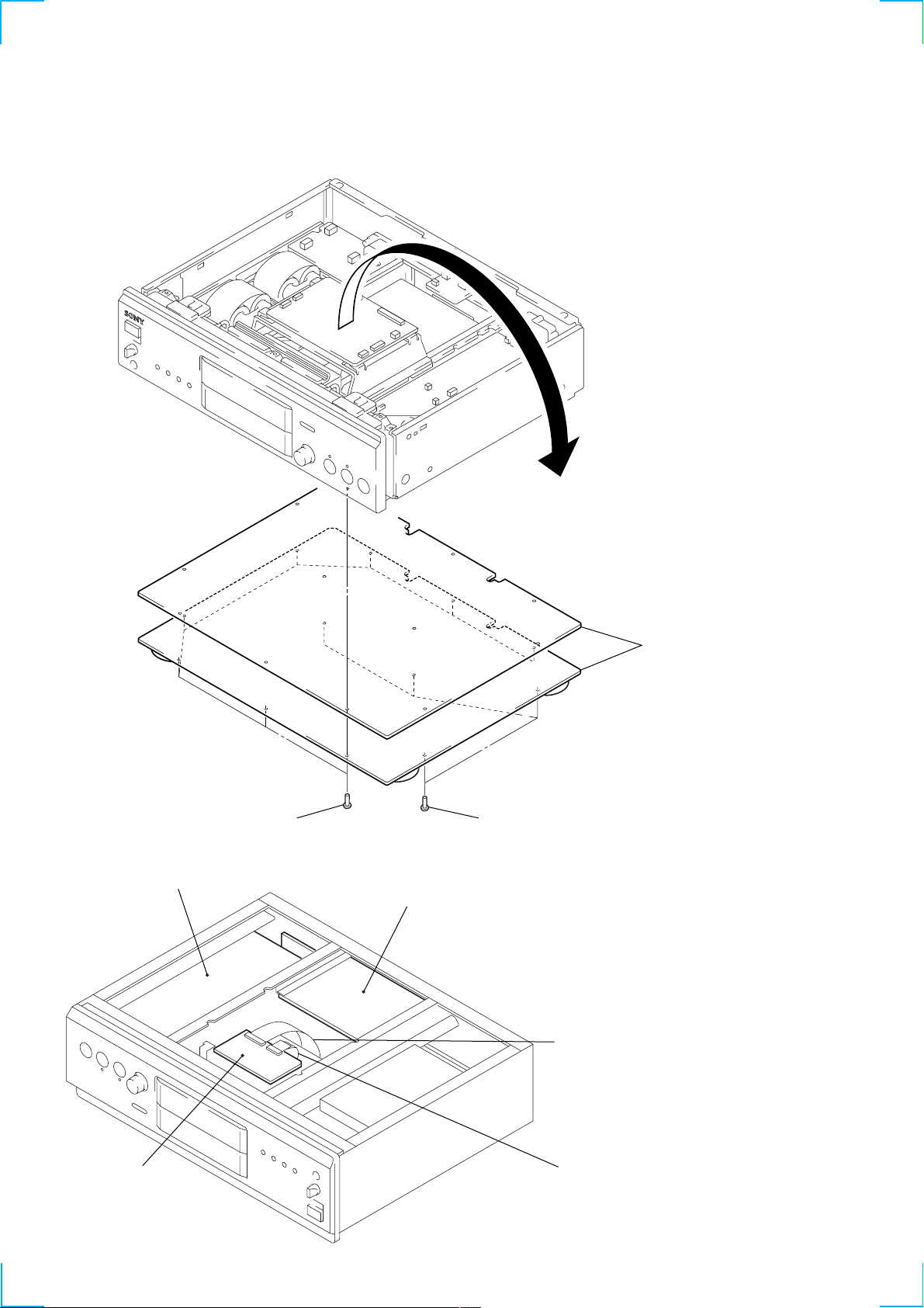
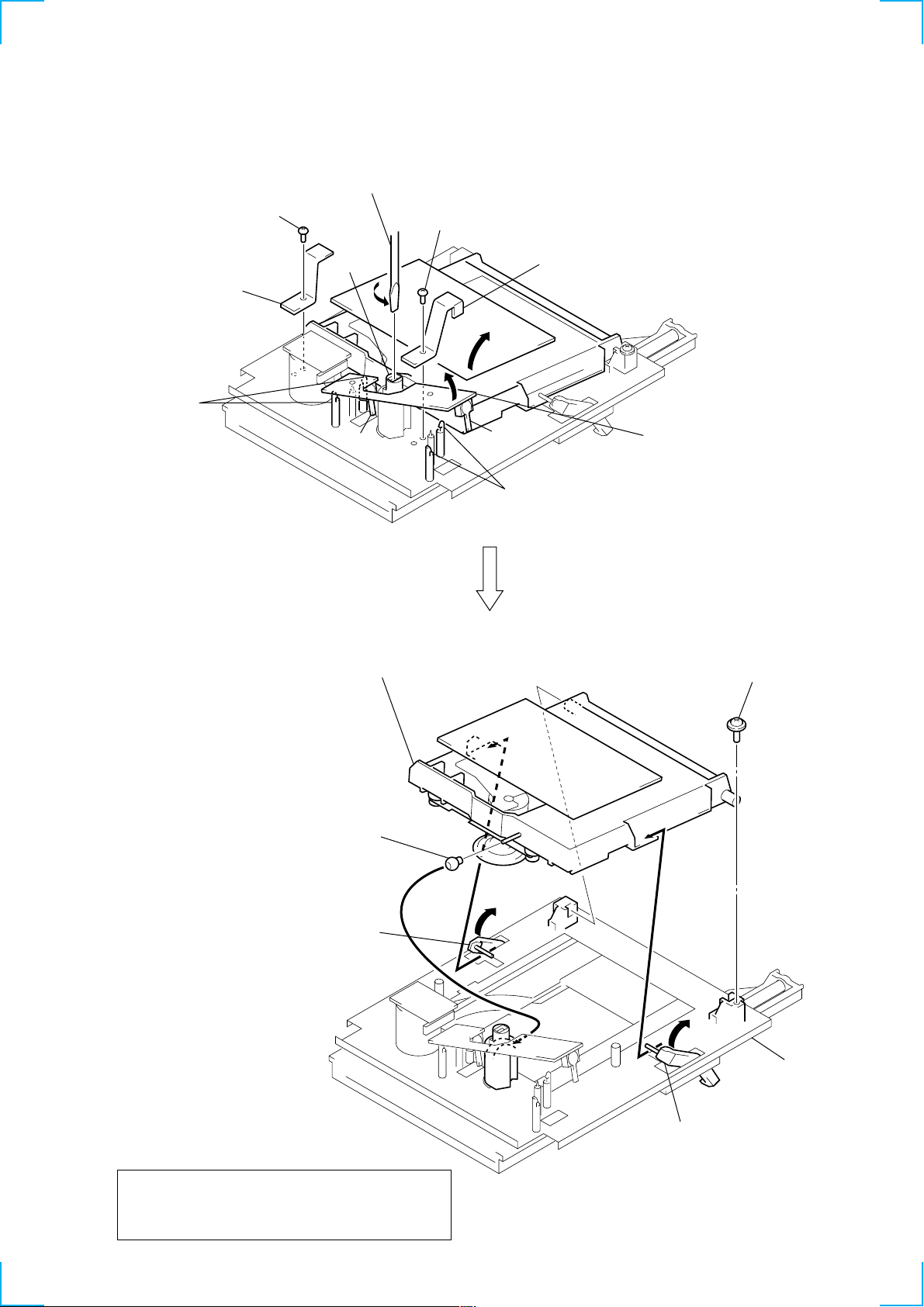
AUDIO/POWER BOARDS AND RF BOARD SERVICE POSITION
1
Remove the case.
2
Turn over the set.
– BOTTOM VIEW –
AUDIO board
3
eight screws (3 × 8)
POWER board
4
two bottom plate
3
four screws (3 × 8)
INSTALLATION TWO WIRES (FLAT TYPE) (25/35 CORE)
Note: When the wire (flat type) (35 core) is disconnected
from the RF board, then it is again connected,
disconnect the wire (flat type) (25 core) once,
and reconnect the wire (flat type) (35 core) first.
wire (flat type) (35 core)
RF board
wire (flat type) (25 core)
4
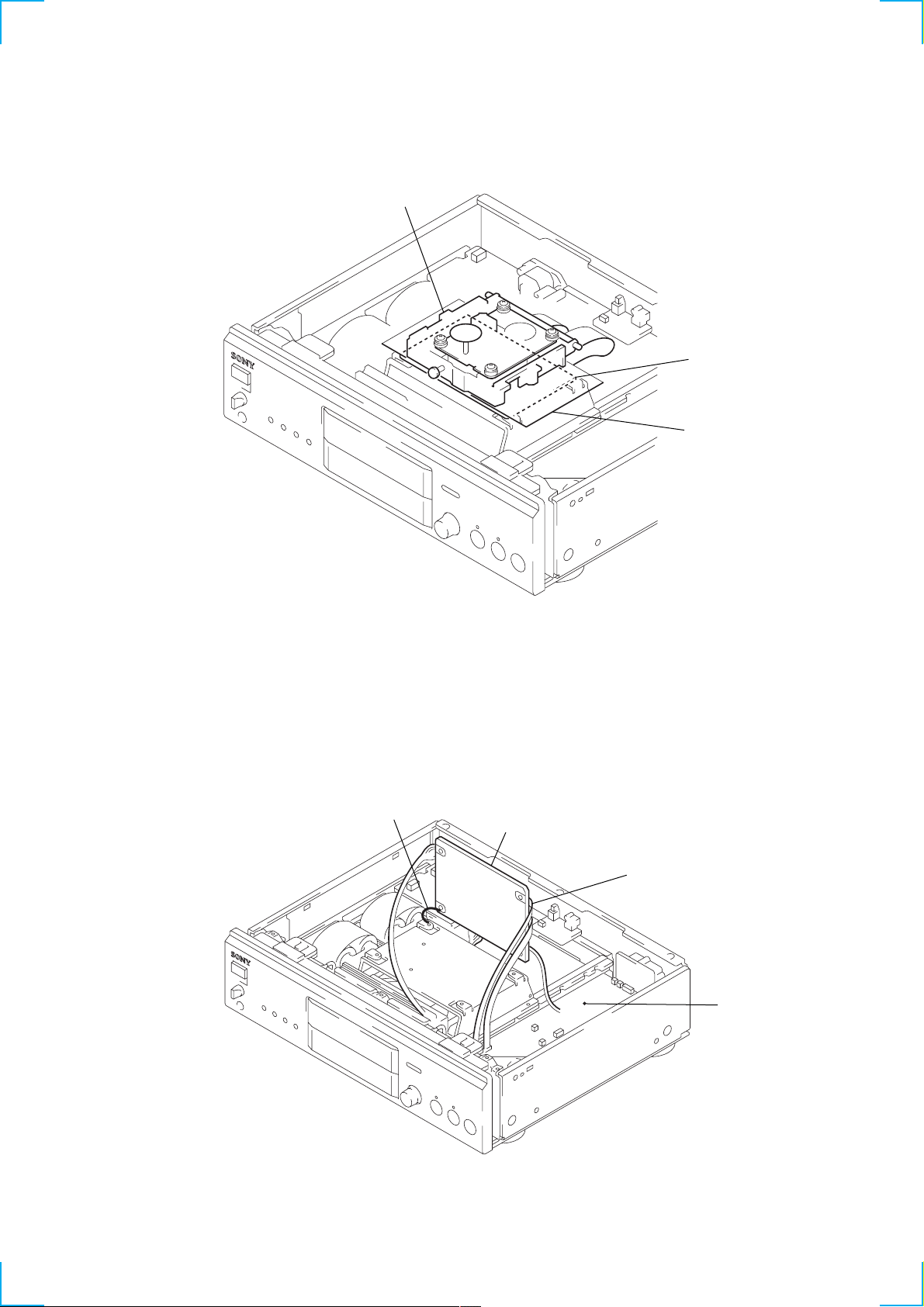
OPTICAL PICK-UP SERVICE POSITION
d
Place the insulator on the MAIN board, then install the base unit (DVBU4) on it as shown in the figure.
base unit
(DVBU4)
MAIN boar
insulator
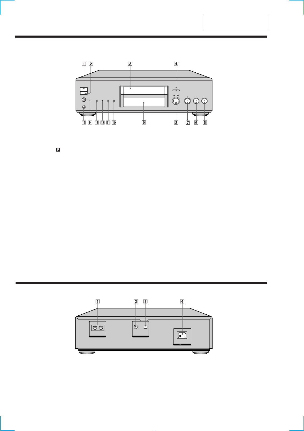
MAIN BOARD SERVICE POSITION
In checking the MAIN board, prepare jig (extension cable J-2501-155-A: 1.00 mm Pitch, 9 cores, Length 300 mm).
Note: Be sure to ground the MAIN board with a lead wire when checking it.
lead wire
MAIN board
connect jig (extension cable
J-2501-155-A) to the MAIN
board (CN902) and AUDIO
board (CN308).
AUDIO board
5
Front Panel Parts
Descriptions
SECTION 2
GENERAL
This section is extracted from
instruction manual.
1 POWER switch (11)
Press to turn on/off the player.
2 Remote sensor
(4)
3 Disc tray (11)
Press A OPEN/CLOSE to open/
close the disc tray.
4 A OPEN/CLOSE button (11)
Press to open/close the disc tray.
5 x button (12)
Press to stop play.
6 X button (12)
Press to pause play.
X indicator
Lights up during pause.
7 N button (11)
Press to start play.
N indicator
Lights up during playback.
POWER
PHONE LEVEL
MIN MAX
PHONES
TIME/TEXT SACD/CD
DIGITAL OUTFILTER
8 lAMSL dial (AMS:
Automatic Music Senser) (11)
When you turn the lAMSL
dial counterclockwise by one click,
you go back to the preceding track;
when you turn the lAMSL
dial clockwise by one click, you go
to the succeeding track.
9 Display window (12)
Shows various information.
0 SACD/CD button (with an LED)
(11)
Each time you press the button
while the Hybrid disc (page 11) is
loaded, the layer changes between
the HD layer (the LED turns on) and
CD layer (the LED turns off).
qa DIGITAL OUT button (with an LED)
(5)
Press when a component is
connected to the DIGITAL (CD)
OUT connectors. Each time you
OPEN/CLOSE
AMS
PUSH ENTER
press the button, the DIGITAL OUT
mode changes between ON (the
digital signals can be output/the
LED turns on) and OFF (the digital
signals cannot be output/the LED
turns off). The digital signal can be
output only when you play a CD.
qs FILTER button (18)
Press to select a digital filter type
when playing a CD.
qd TIME/TEXT button (12)
Each time you press the button, the
playing time of the track, the total
remaining time on the disc, or TEXT
information appears in the display.
qf PHONE LEVEL
Adjust the headphones volume.
qg PHONES
Connect the headphones.
Rear Panel Parts Descriptions
R
L
OUT
ANALOG
1 ANALOG OUT jacks (5)
Connect to an audio component using the audio
connecting cord.
2 DIGITAL (CD) OUT COAXIAL connector (5)
Connect to an audio component using the coaxial
digital cable.
3 DIGITAL (CD) OUT OPTICAL connector (5)
Connect to an audio component using an optical
digital cable.
6
COAXIAL
OPTICAL
OUT
DIGITAL (CD)
AC IN
4 AC IN terminal (5)
Connect the mains lead.
Note
Only the audio signals of the CD can be output from the
DIGITAL (CD) OUT connectors shown in 2 and 3 . Those of
the Super Audio CD cannot be output through DIGITAL (CD)
OUT connectors.
Remote Parts Descriptions
1 CONTINUE button (17)
Press to resume normal play from Shuffle Play or
Programme Play.
SHUFFLE button (17)
Press to select Shuffle Play.
PROGRAM button (17)
Press to select Programme Play.
2 SACD/CD button (11)
Each time you press the button while the Hybrid disc
(page 11) is loaded, the layer changes between an HD
layer (the SACD/CD LED turns on) and CD layer (the
SACD/CD LED turns off).
3 DISPLAY MODE button (13)
Press to turn off the information.
4 Number buttons (14)
Press to enter the track numbers.
5
i
10 button (14)
Press to locate a track numbered over 10.
6 REPEAT button (16)
Press repeatedly to play all tracks or only one track on
the disc.
7 H button (11)
Press to start play.
X button (12)
Press to pause play.
x button (12)
Press to stop play.
8 AMS ./> (AMS: Automatic Music Sensor)
buttons (14)
Press to locate a specific track.
9 m/M buttons (15)
Press to locate a portion you want to play within a
track.
qa TIME/TEXT button (12)
Each time you press the button, the playing time of the
track, the total remaining time on the disc, or TEXT
information appears in the display.
qs LANGUAGE button (14)
Press to change the displayed language if the TEXT
disc has several languages.
qd DIGITAL FILTER button (18)
Press to select a digital filter type when playing a CD.
qf CLEAR button (17)
Press to delete a programmed track number.
qg CHECK button (18)
Press to check the programmed order.
qh AyB button (16)
Press to select Repeat A-B Play.
PLAY MODE
CONTINUE SHUFFLE
SACD/CD
PROGRAM
TIME/
TEXT
LANGUAGE
DISPLAY/ DIGITAL/
MODE
FILTER
123
456
78
>10 CLEAR
REPEAT
CLEAR
9
10/0
BA CHECK
0 INDEX >/. buttons (15)
Press to locate a specific point marked with an index
signal when you play a disc that has index signals.
AMS
INDEX
7
Compatible Disc Types
You can play the following discs with this player.
Depending on the type of disc to be played, select the
appropriate indicator by pressing SACD/CD on the front
panel of the player or on the remote (pages 11).
Super Audio CD (single layer disc)
This disc consists of a single HD layer*.
Press SACD/CD repeatedly so that “SUPER AUDIO CD”
appears in the display (the SACD/CD LED turns on).
*High density signal layer for the Super Audio CD
HD (high density) layer
Super Audio CD (dual layer disc)
This disc consists of dual HD layers and is capable of
extended play over long periods.
Press SACD/CD repeatedly so that “SUPER AUDIO CD”
appears in the display (the SACD/CD LED turns on).
Also, as the dual layer disc consists of dual HD layers on
one side only, it is not necessary to turn the disc over.
Super Audio CD + CD (Hybrid disc)
This disc consists of an HD layer and a CD layer. Press
SACD/CD to select the layer you want to listen to. Also,
as the dual layers are on one side, it is not necessary to
turn the disc over. You can play the CD layer using a
conventional CD player.
CD layer
HD layer
Incompatible Discs
This player cannot play the following discs. If you try to
play them, the error message “TOC Error” or “NO DISC”
will appear or there will be no sound.
• CD-ROM
• DVD, etc.
HD layer
HD layer
Conventional CD
This disc is the standard format.
Press SACD/CD repeatedly so that “CD” appears in the
display (the SACD/CD LED turns off).
CD layer
8
• This set can be disassembled in the order shown below.
1
flat head screw (TP)
4
case
1
two flat head screws (TP)
1
two flat head screws
(TP)
2
2
3
SECTION 3
DISASSEMBLY
SET
CASE
(Page 9)
LOADING PANEL ASS’Y
(Page 10)
FRONT PANEL SECTION
(Page 10)
DISC TABLE, BELT, LOADING MOTOR (M1)
(Page 12)
Note: Follow the disassembly procedure in the numerical order given.
MECHANISM DECK (CDM19HN-DVBU4), RF BOARD
OPTICAL PICK-UP
(KHM-230AAA/J1NP)
After removing the base unit (DVBU4), the optical pick-up (KHM-230AAA/J1NP)
can be removed.
CASE
(Page 11)
(Page 12)
MAIN BOARD, BRACKET (MAIN)
(Page 11)
BASE UNIT (DVBU4)
(Page 13)
9
LOADING PANEL ASSY
5
loading panel ass’y
4
bracket (loading panel)
3
two screws
(P3 × 10)
2
A
cover (CAM)
1
Insert a tapering driver in the hole
at the bottom of the unit,
turn the cover (CAM) fully in the
direction of arrow A.
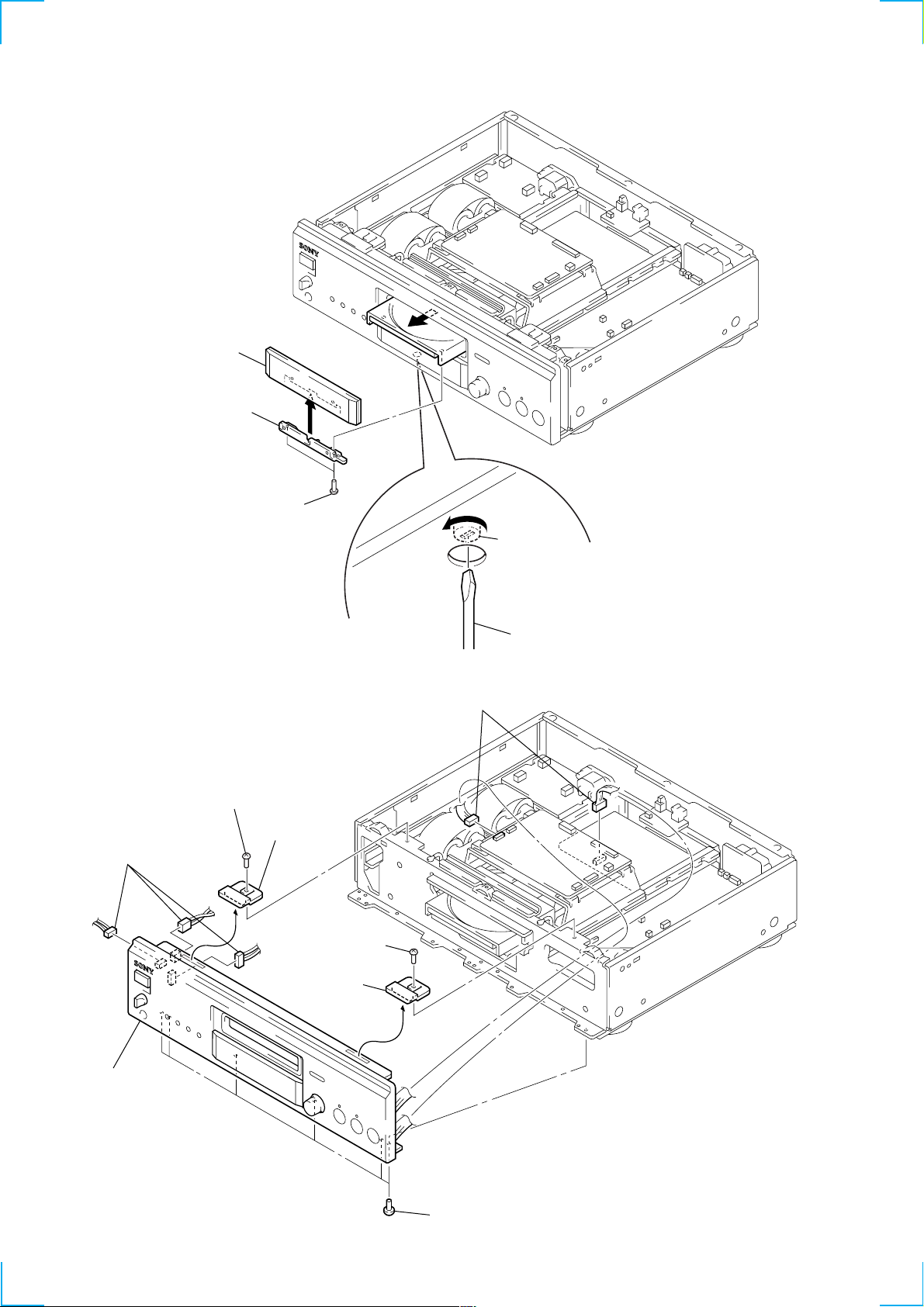
FRONT PANEL SECTION
3
screw (3 × 8)
2
three connectors
(CN371, 372, 481)
5
front panel section
4
bracket (F)
4
3
screw (3 × 8)
bracket (F)
2
two connectors
(CN408, 903)
tapering driver
10
1
six screws
(3
×
8)
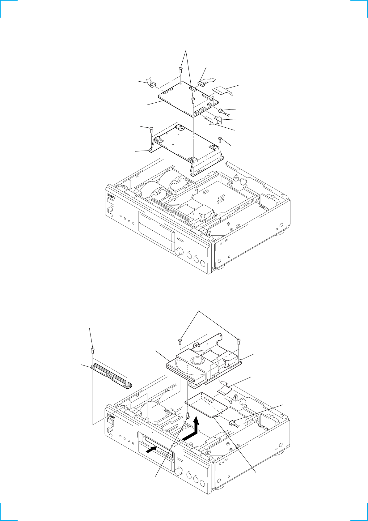
MAIN BOARD, BRACKET (MAIN)
)
2
two screws
(3
×
8)
3
bracket
(guide wire)
1
Push the disc table in the
direction of arrow
A
.
9
three screws
(BVTP2.6
×
8)
0
RF board
8
connector
(CN002)
7
wire (flat type) (25 core)
(CN003)
6
mechanism deck (CDM19HN-DVBU4)
4
four screws (3 × 8)
disc table
A
5
2
connector
(CN903)
4
MAIN board
5
two screws
(3
×
8)
6
bracket (main)
3
four screws (3 × 8)
2
connector
(CN701)
1
wire (flat type) (35 core
(CN503)
2
connector (CN904)
1
wire (flat type) (16 core)
(CN901)
1
wire (flat type) (9 core)
(CN902)
5
two screws
×
8)
(3
MECHANISM DECK (CDM19HN-DVBU4), RF BOARD
11
)
DISC TABLE, BELT, LOADING MOTOR (M1)
8
guide bar (main)
9
disc table
2
holder (A. P.) ass’y
1
two screws
(BVTT M3 S
7
6
bracket (disc table)
5
tapping screw
3
Insert a tapering driver in the
hole of the cover (CAM) and
turn fully in the direction of
arrow
A
.
cover (CAM)
OPTICAL PICK-UP (KHM-230AAA/J1NP)
1
2
holder (A. P.) ass’y
two screws
(BVTT M3 S)
6
7
9
insulator
4
qa
0
gear (P)
A
taper driver
screw
(BVTP2.6
stopper
gear (C)
×
8)
9
qf
6
screw
(BVTP2.6
insulator
qs
belt
four claws
×
8)
7
qd
two screws
(P3
×
3)
qg
loading motor (M1)
stopper
0
optical pick-up (KHM-230AAA/J1NP)
6
screw
(BVTP2.6
7
stopper
9
insulator
9
insulator
×
8)
12
6
screw
(BVTP2.6
4
Draw out the disc table fully
in the arrow
B
B
direction.
×
8)
7
stopper
8
A
taper driver
5
wire (flat type) (25 core)
(CN003)
two cone type coil spring (230)
qa
qa
two cone type coil spring (230)
3
Insert a tapering driver in the
hole of the cover (CAM) and
turn fully in the direction of
A
arrow
.
cover (CAM)
BASE UNIT (DVBU4)
5
screw
(BVTT3
6
limiter (R)
1
two claws
7
Insert a taper driver into the cover (CAM),
and rotate in the arrow
the base unit (DVBU4) in the arrow
(Chuck release state)
×
6)
cover (CAM)
B
B
direction to raise
3
screw
(BVTT3
A
C
×
C
direction.
6)
4
limiter (L)
S001
9
Raising the stable lock (L/R) Ass’y simultaneously
in the arrow D direction, remove the base unit (DVBU4)
from the chassis (outseat).
Note: The stable lock (L/R) Ass’y will attempt to
return in the reverse direction of arrow
by a spring force. Therefore, take care not
to break the shaft of stable lock (L/R) Ass’y
when removing the stable lock (L/R) Ass’y
from the base unit (DVBU4).
0
D
roller (L)
S002
1
two claws
2
Up the SWITCH board in the
direction of arrow
Note: Take care not to break the shaft of
the switch (S001, S002) when raising
the SWITCH board.
8
A
.
screw (PTPWH3 × 8)
stable lock (R) ass’y
In removing the optical pick-up (KHM-230AAA/J1NP)
after removing the base unit (DVBU4),
perform the optical pick-up (KHM-230AAA/J1NP) removal
procedure after step 5 on page 12.
D
D
chassis (outseat)
stable lock (L) ass’y
13

MEMO
14

4-25. IC PIN FUNCTION DESCRIPTION
• MAIN BOARD IC509 CXD3008Q
(DIGITAL SIGNAL PROCESSOR, DIGITAL SERVO PROCESSOR, DIGITAL FILTER, D/A CONVERTER)
Pin No. Pin Name I/O Description
1 DVDD0 —
2 XRST I
3 MUTE I
4 DATA I
5 XLAT I
6 CLOK I
7 SENS O
8 SCLK I
9 ATSK I
10 WFCK O
11 XUGF O
12 XPCK O
13 GFS O
14 C2PO O
15 SCOR O
16 C4M O
17 WDCK O
18 DVSS0 —
19 COUT O
20 MIRR O
21 DFCT O
22 FOK O
23 PWMI I
24 LOCK O
25 MDP O
26 SSTP I
27 FSTO O
28 DVDD1 —
29 SFDR O
30 SRDR O
31 TFDR O
32 TRDR O
33 FFDR O
34 FRDR O
35 DVSS1 —
36 TEST I
37 TES1 I
38 VC I
39 FE I
40 SE I
41 TE I
42 CE I
43 RFDC I
44 ADIO O
Power supply terminal (+5V) (digital system)
Reset signal input from the expander (IC902) “L”: reset
Muting control signal input from the CPU (IC901) “H”: muting
Serial data input from the CPU (IC901)
Latch signal input from the CPU (IC901)
Clock signal input from the CPU (IC901)
Internal status (SENSE) signal output to the CPU (IC901)
Serial data transfer clock input from the CPU (IC901)
Input pin for anti-shock (fixed at “L”)
Write frame clock signal output to the SACD decoder (IC701)
XUGF signal output terminal Not used (open)
XPCK signal output terminal Not used (open)
Guard frame sync signal output to the CPU (IC901)
C2 pointer signal output to the SACD decoder (IC701)
Subcode sync OR signal output to the SACD decoder (IC701) and the CPU (IC901)
4.2336 MHz clock signal output terminal Not used (open)
Guard subcode sync OR signal output to the SACD decoder (IC701)
Ground terminal (digital system)
Numbers of track counted signal output to the CPU (IC901)
Mirror signal output to the CPU (IC901)
Defect signal output terminal Not used (pull up)
Focus OK signal output to the CPU (IC901)
Not used (fixed at “L”)
GFS is sampled by 460 Hz “H” output when GFS is “H”
Spindle motor (M3) servo drive signal output to the SACD decoder (IC701)
Detection signal input from limit switch (S1) The optical pick-up is inner position when “H”
2/3 divider output terminal Not used (open)
Power supply terminal (+5V) (digital system)
Sled servo drive PWM signal (+) output to the BA5938FP (IC502)
Sled servo drive PWM signal (–) output to the BA5938FP (IC502)
Tracking servo drive PWM signal (+) output to the BA5938FP (IC502)
Tracking servo drive PWM signal (–) output to the BA5938FP (IC502)
Focus servo drive PWM signal (+) output to the BA5938FP (IC502)
Focus servo drive PWM signal (–) output to the BA5938FP (IC502)
Ground terminal (digital system)
Input terminal for the test (fixed at “L”)
Input terminal for the test (fixed at “L”)
Middle point voltage (+1.65V) input from the NJM3403AV (IC009)
Focus error signal input from the CXD1881R (IC001)
Sled error signal input from the CXD1881R (IC001)
Tracking error signal input from the CXD1881R (IC001)
Chip enable signal input from the CXD1881R (IC001)
RF signal (DC level) input from the CXD1881R (IC001)
Output terminal for the A/D converter Not used (open)
47

Pin No. Pin Name I/O Description
45 AVSS0 —
46 IGEN I
47 AVDD0 —
48 ASYO O
49 ASYI I
50 RFAC I
51 AVSS1 —
52 CLTV I
53 FILO O
54 FILI I
55 PCO O
56 AVDD1 —
57 BIAS I
58 VCTL I
59 V16M O
60 VPCO O
61 DVDD2 —
62 ASYE I
63 MD2 I
64 DOUT O
65 LRCK O
66 PCMD O
67 BCLK O
68 EMPH O
69 XTSL I
70 DVSS2 —
71 XTAI I
72 XTAO O
73 SOUT O
74 SOCK O
75 XOLT I
76 SQSO O
77 SQCK I
78 SCOR O
79 SBSO O
80 EXCK I
Ground terminal (analog system)
Stabilized current input for operational amplifiers
Power supply terminal (+5V) (analog system)
Playback EFM full-swing output terminal
Playback EFM asymmetry comparator voltage input terminal
EFM RF signal (AC level) input from the CXD1881R (IC001)
Ground terminal (analog system)
Internal VCO control voltage input of the EFM playback master PLL
Filter output for master clock of the playback EFM master PLL
Filter input for master clock of the playback EFM master PLL
Phase comparison output for master clock of the playback EFM master PLL
Power supply terminal (+5V) (analog system)
Playback EFM asymmetry circuit constant current input terminal
Control voltage input terminal for the variable pitch Not used (fixed at “L”)
16.9344 MHz clock signal output Not used (open)
PLL charge pump output terminal for the variable pitch Not used (fixed at “L”)
Power supply terminal (+5V) (digital system)
Playback EFM asymmetry circuit on/off selection signal input terminal
Not used (fixed at “H”)
Digital out on/off control signal input from the CPU (IC901)
“L”: digital out on, “H”: digital out off
Digital audio signal output to the DIGITAL (CD) OUT OPTICAL (IC392)
L/R sampling clock signal (44.1 kHz) output to the digital filter (IC301) and SACD decoder
(IC701)
Serial data output to the digital filter (IC301) and SACD decoder (IC701)
Bit clock signal (2.8224 MHz) output to the digital filter (IC301) and SACD decoder (IC701)
Playback disc output terminal in emphasis mode Not used (open)
Input terminal for the system clock frequency setting Fixed at “H” in this set
Ground terminal (digital system)
System clock input terminal (33.86688 MHz)
System clock output terminal (33.86688 MHz) Not used (open)
Not used (open)
Not used (open)
Not used (open)
Subcode Q data output to the CPU (IC901)
Subcode Q data reading clock signal input from the CPU (IC901)
Not used (open)
Subcode serial data output to the SACD decoder (IC701)
Subcode serial data reading clock signal input to the SACD decoder (IC701)
48

• MAIN BOARD IC701 CXD1882R (SACD DECODER)
Pin No. Pin Name I/O Description
1, 2 D5, D6 I/O
3 VSS —
4 D7 I/O
5A0I
6 VDD —
7A1I
8 VDD5V —
9 to 14 A2 to A7 I
15 VSS —
16 XWAIT O
17 XRD I
18 XWR I
19 XCS I
20, 21 XINT0, XINT1 O
22 VDD —
23 XHRS I
24 HDB7 O
25 VSS —
26 HDB8 O
27 HDB6 O
28 VDDS —
29 HDB9 O
30 HDB5 O
31 HDBA O
32 HDB4 O
33 VSS —
34 HDBB O
35 HDB3 O
36 VDD —
37 HDBC O
38 VDDS —
39 HDB2 O
40 HDBD O
41 HDB1 O
42 VSS —
43 HDBE O
44 HDB0 O
45 HDBF O
46 XACK O
47 VDDS —
48 DCK O
49 XSHDR0 O
50 VDD —
51 REDY O
52 VSS —
53 REQUEST I
Two-way data bus with the CPU (IC901) and expander (IC902)
Ground terminal (digital system)
Two-way data bus with the CPU (IC901) and expander (IC902)
Address signal input from the CPU (IC901)
Power supply terminal (+3.3V) (digital system)
Address signal input from the CPU (IC901)
Power supply terminal (+5V)
Address signal input from the CPU (IC901)
Ground terminal (digital system)
Wait signal output terminal Not used (open)
Read strobe signal input from the CPU (IC901)
Write strobe signal input from the CPU (IC901)
Chip select signal input from the CPU (IC901)
Interrupt signal output to the CPU (IC901)
Power supply terminal (+3.3V) (digital system)
Not used (open)
Stream data signal output to the DSD decoder (IC801)
Ground terminal (digital system)
Error flag signal output to the DSD decoder (IC801)
Stream data signal output to the DSD decoder (IC801)
Power supply terminal (+5V) (digital system)
Not used (open)
Stream data signal output to the DSD decoder (IC801)
Not used (open)
Stream data signal output to the DSD decoder (IC801)
Ground terminal (digital system)
Not used (open)
Stream data signal output to the DSD decoder (IC801)
Power supply terminal (+3.3V) (digital system)
Not used (open)
Power supply terminal (+5V) (digital system)
Stream data signal output to the DSD decoder (IC801)
Not used (open)
Stream data signal output to the DSD decoder (IC801)
Ground terminal (digital system)
Not used (open)
Stream data signal output to the DSD decoder (IC801)
Not used (open)
Serial data transfer acknowledge signal output to the DSD decoder (IC801)
Power supply terminal (+5V) (digital system)
Serial data transfer clock signal output to the DSD decoder (IC801)
Header flag signal output to the DSD decoder (IC801)
Power supply terminal (+3.3V) (digital system)
Not used (pull up)
Ground terminal (digital system)
Serial data transfer request signal input from the DSD decoder (IC801)
49

Pin No. Pin Name I/O Description
6
54 HINT O
55 XS16 O
56 HA1 I
57 XPDI I/O
58 VDDS —
59, 60 HA0, HA2 I
61 VSS —
62, 63 HCS0, HCS1 I
64 VDD —
65 DASP I/O
66 to 69 MDB0 to MDB3 I/O
70 VSS —
71 MDB4 I/O
72 VDD5V —
73 to 75 MDB5 to MDB7 I/O
76 XMWR O
77 VDD —
78 XRAS O
79, 80 MA0, MA1 O
81 VSS —
82 to 87 MA2 to MA7 O
88 VDD —
89 MA8 O
90 VSS —
91 MA9/MNT0 O
92 MA10/MNT1 O
93 MA11/MNT2 O
94 XMOE O
95 XCAS O
96, 97 MDB8, MDB9 I/O
98 VSS —
99 MDBA I/O
100 VDD —
101, 102 MDBB, MDBC I/O
103 VDD5V —
104 to 10
113, 114 ASF1, AFS2 —
MDBD to MDBF I/O
107 GFS O
108 VSS —
109 APEO O
110 VDD —
111 DASYO O
112 GNDA5 —
115 DASYI I
116 RFDCC I
117 RF IN I
Not used (pull up)
Not used (pull up)
Not used (fixed at “H” )
Not used (pull up)
Power supply terminal (+5V) (digital system)
Not used (fixed at “H” )
Ground terminal (digital system)
Not used (open)
Power supply terminal (+3.3V) (digital system)
Not used (pull up)
Two-way data bus with the D-RAM (IC706)
Ground terminal (digital system)
Two-way data bus with the D-RAM (IC706)
Power supply terminal (+5V)
Two-way data bus with the D-RAM (IC706)
Write enable signal output to the D-RAM (IC706)
Power supply terminal (+3.3V) (digital system)
Row address strobe signal output to the D-RAM (IC706)
Address signal output to the D-RAM (IC706)
Ground terminal (digital system)
Address signal output to the D-RAM (IC706)
Power supply terminal (+3.3V) (digital system)
Address signal output to the D-RAM (IC706)
Ground terminal (digital system)
Address signal output to the D-RAM (IC706)
RF data signal output terminal for disc mark detection
Clock signal output terminal for disc mark detection
Monitor signal output to the CPU (IC901)
Output enable signal output to the D-RAM (IC706)
Column address strobe signal output to the D-RAM (IC706)
Two-way data bus with the D-RAM (IC706)
Ground terminal (digital system)
Two-way data bus with the D-RAM (IC706)
Power supply terminal (+3.3V) (digital system)
Two-way data bus with the D-RAM (IC706)
Power supply terminal (+5V)
Two-way data bus with the D-RAM (IC706)
Guard frame sync signal output to the CPU (IC901)
Ground terminal (digital system)
Absolute phase error signal output
Power supply terminal (+3.3V) (digital system)
RF binary signal output
Ground terminal (analog system)
Filter connected terminal for selection the constant asymmetry compensation
Analog signal input after integrated from the RF binary signal
Input terminal for adjusting DC cut high-pass filter for RF signal
RF signal input from the CXD1881R (IC001)
50

Pin No. Pin Name I/O Description
118, 119 VCCA5, VCCA4 —
120 VCOR1 —
121 VCOIN I
122, 123 GNDA4, GNDA3 —
124 LPF5 O
125 VC1 I
126, 127 LPF2, LPF1 I
128, 129 VCCA3, VCCA2 —
130 PDO O
131 PDHVCC I
132 FDO O
133, 134 GNDA2, GNDA1 —
135 SPO O
136 VC2 I
137 MDIN2 I
138 MDIN1 I
139 VCCA1 —
140 CLVS O
141 VSS —
142 MDSOUT O
143 VDD —
144 MDPOUT O
145 DEFECT I
146 GSCOR I
147 EXCK O
148 SBIN I
149 VSS —
150 SCOR I
151 WFCK I
152 VDD5V —
153 XRCI I
154 VDDS —
155 C2PO I
156 VDD —
157 DBCK O
158 BCLK I
159 DDAT O
160 MDAT I
161 VSS —
162 DLRC O
163 LRCK I
164 XRST I
165 IFS0 I
166 IFS1 I
167 XTAL I
168 VSS —
169 XTA2 O
Power supply terminal (+3.3V) (analog system)
VCO oscillating range setting resistor connected terminal
VCO input terminal
Ground terminal (analog system)
Signal output from the operation amplifier from PLL loop filter
Middle point voltage (+1.65V) input terminal
Inverted signal input to the operation amplifier from PLL loop filter
Power supply terminal (+3.3V) (analog system)
Signal output from the charge pump for phase comparator
Middle point voltage input terminal for RF PLL
Signal output from the charge pump for frequency comparator
Ground terminal (analog system)
Spindle motor (M3) control signal output to the BA5912AFP (IC512)
Middle point voltage (+1.65V) input terminal
Spindle motor (M3) control signal input from the CXD3008Q (IC509)
MDP input terminal
Power supply terminal (+3.3V) (analog system)
Control signal output for selection the spindle control filter at CLVS
Ground terminal (digital system)
Frequency error output terminal of internal CLV circuit
Power supply terminal (+3.3V) (digital system)
Phase error output terminal of internal CLV circuit
Defect signal input terminal Not used (fixed at “L” )
Guard subcode sync OR signal input from the CXD3008Q (IC509)
Subcode serial data reading clock signal output to the CXD3008Q (IC509)
Subcode serial data input from the CXD3008Q (IC509)
Ground terminal (digital system)
Subcode sync OR signal input from the CXD3008Q (IC509)
Write frame clock signal input from the CXD3008Q (IC509)
Power supply terminal (+5V)
RAM overflow signal input terminal Not used (fixed at “L” )
Power supply terminal (+5V) (digital system)
C2 pointer signal input from the CXD3008Q (IC509)
Power supply terminal (+3.3V) (digital system)
Bit clock signal (2.8224 MHz) output terminal Not used (open)
Bit clock signal (2.8224 MHz) input from the CXD3008Q (IC509)
PCM data output terminal Not used (open)
Serial data input from the CXD3008Q (IC509)
Ground terminal (digital system)
L/R sampling clock signal (44.1 kHz) output terminal Not used (open)
L/R sampling clock signal (44.1 kHz) input from the CXD3008Q (IC509)
Reset signal input from the expander (IC902) “L”: reset
Interface select signal input terminal Fixed at “L” in this set
Interface select signal input terminal Fixed at “H” in this set
33.86688 MHz clock signal input terminal
Ground terminal (digital system)
System clock output terminal (33.86688 MHz)
51

Pin No. Pin Name I/O Description
6
170 XTA1 I
171 VDD —
172 to 17
D0 to D4 I/O
System clock input terminal (33.86688 MHz)
Power supply terminal (+3.3V) (digital system)
Two-way data bus with the CPU (IC901) and expander (IC902)
52
• MAIN BOARD IC801 CXD2751Q (DSD DECODER)
Pin No. Pin Name I/O Description
1 XSRQ O
2 XSHD I
3VDD—
4VSS—
5 SDCK I
6 SMUTE I
7 XMSLAT I
8 MSCK I
9 MSDATI I
10 MSDATO O
11 MSREDY I
12 XMSDOE O
13 XRST I
14 MCKI I
15 VSS —
16 CK75S I
17 EXCKO1 O
18 EXCKO2 O
19 LRCK I/O
20 UBIT —
21 MNT2 O
22 TRST I
23 TCK I
24 TDI I
25 TENA1 I
26 TDO O
27 VST —
28 VDD —
29 VSS —
30 MNT1 O
31 MNT0 O
32 XBIT O
33 F75HZ O
34 SUPDAT O
35 SUPAK O
36 SUPEN O
37 TEST1 I
38 VSS —
39 TEST2 I
40, 41 VSS —
42 BCKD I
43 DSDL —
44 DSDR —
45 MUDAT —
46 BCKA I
47 DSAL O
Serial data transfer request signal output to the SACD decoder (IC701)
Header flag signal input from the SACD decoder (IC701)
Power supply terminal (+3.3V) (digital system)
Ground terminal (digital system)
Serial data transfer clock signal input from the SACD decoder (IC701)
Muting signal input from the CPU (IC901) “L”: muting
Latch signal input from the CPU (IC901)
Serial data transfer clock signal input from the CPU (IC901)
Serial data input from the CPU (IC901)
Serial data output to the CPU (IC901)
Ready signal input from the CPU (IC901) “L”: ready
Data enable signal output terminal Not used (open)
Reset signal input from the expander (IC902) “L”: reset
Master clock signal input terminal
Ground terminal (digital system)
Master clock selection signal input terminal “L”: 512fs, “H”: 768fs (fixed at “H” in this set)
External clock 1 signal output terminal
External clock 2 signal output terminal Not used (open)
L/R sampling clock signal (44.1kHz) input/output terminal Not used (open)
Not used (open)
Monitor 2 signal output terminal Not used (open)
Reset signal input terminal “L”: reset Not used (fixed at “L”)
Clock signal input terminal for test (normally: fixed at “L”)
Serial data input terminal for test (normally: open)
Enable signal input terminal for test (normally: open)
Serial data output terminal for test (normally: open)
Ground terminal for test (digital system)
Power supply terminal (+3.3V) (digital system)
Ground terminal (digital system)
Monitor 1 signal output terminal Not used (open)
Monitor 0 signal output terminal Not used (open)
Bit clock signal (2.8224 MHz) output terminal Not used (open)
Clock signal (75 Hz) output terminal Not used (open)
Serial data output terminal Not used (open)
Acknowledge signal output terminal Not used (open)
Enable signal output terminal Not used (open)
Test 1 signal input terminal for test (normally: fixed at “L”)
Ground terminal (digital system)
Test 2 signal input terminal for test (normally: fixed at “L”)
Ground terminal (digital system)
Shift clock signal input from the digital filter (IC301)
Not used (open)
Not used (open)
Not used (open)
Shift clock signal input from the digital filter (IC301)
DSD data (Lch) output to the digital filter (IC301)
53

Pin No. Pin Name I/O Description
48 DSAR O
49 ZDFLGL O
50 ZDFLGR O
51, 52 A0, A1 O
53 VDD —
54 VSS —
55 to 63 A2 to A10 O
64 NC —
65 VSS —
66 XWE O
67 XCAS O
68 XRAS O
69 XOE O
70 to 77 DQ0 to DQ7 I/O
78 VDD —
79 VSS —
80 WCK I
81 WRFD I
82 to 89 WAD0 to WAD7 I
90 VSS —
91 to 98 SD7 to SD0 I
99 SDEF I
100 XSAK I
DSD data (Rch) output to the digital filter (IC301)
Data (Lch) flag detection signal output terminal Not used (open)
Data (Rch) flag detection signal output terminal Not used (open)
Address signal output to the D-RAM (IC808)
Power supply terminal (+3.3V) (digital system)
Ground terminal (digital system)
Address signal output to the D-RAM (IC808)
Not used (open)
Ground terminal (digital system)
Write enable signal output to the D-RAM (IC808)
Column address strobe signal output to the D-RAM (IC808)
Row address strobe signal output to the D-RAM (IC808)
Output enable signal output to the D-RAM (IC808)
Two-way data bus with the D-RAM (IC808)
Power supply terminal (+3.3V) (digital system)
Ground terminal (digital system)
Clock signal input terminal for disc mark detection
RF data signal input terminal for disc mark detection
A/D data signal input from the A/D converter (IC804) for disc mark detection
Ground terminal (digital system)
Stream data signal input from the SACD decoder (IC701)
Error flag signal input from the SACD decoder (IC701)
Serial data transfer acknowledge signal input from the SACD decoder (IC701)
54

• MAIN BOARD IC901 CXP973F064R-1 (CPU)
Pin No. Pin Name I/O Description
1 MODE DF O
2 AMUTE O
3 DOCTRL O
4 LAT DAC O
5 DATA DAC O
6 CLK DAC O
7 FCS JMP 1 O
8 FCS JMP 2 O
9 SENS CD I
10 XCS DRAM O
11 XCS IO O
12 XCS DVD O
13 VSS —
14 to 21 D0 to D7 I/O
22 INT0 DVD I
23 INT1 DVD I
24 T SENS I
25 MON DVD I
26 DATA CD O
27 XLAT CD O
28 A1IN I
29 CONT CD I
30 IN SW I
31 OUT SW I
32 MIRR RF I
33 SUBQ CD I
34 SCOR CD I
35 SQCLK CD O
36 ——
37 CLOK CD O
38 XRST I
39 VSS —
40 XTAL I
41 EXTAL O
42 VDD —
43 LDON RF O
44 XDIS IO O
45 MUTE DSD O
46 XLAT DSD O
47 READY DSD O
48 SDIN DSD I
49 SOUT DSD O
SACD/CD mode selection signal output to the digital filter (IC301) and D/A converter (IC302)
“L”: CD mode, “H”: SACD mode
Muting signal output to the analog line circuit “H”: muting
Digital out on/off control signal output to the CXD3008Q (IC509)
“L”: digital out off, “H”: digital out on
Latch signal output to the D/A converter (IC904)
Serial data output to the D/A converter (IC904)
Clock signal output to the D/A converter (IC904)
Focus jump 1 signal output to the BA5983FP (IC502)
Focus jump 2 signal output to the BA5983FP (IC502)
Internal status (SENSE) signal input from the CXD3008Q (IC509)
Chip select signal output terminal Not used (pull up)
Chip select signal output to the expander (IC902)
Chip select signal output to the SACD decoder (IC701)
Ground terminal (digital system)
Two-way data bus with the SACD decoder (IC701) and expander (IC902)
Interrupt signal input from the SACD decoder (IC701)
Interrupt signal input from the SACD decoder (IC701)
Disc tray status detection signal input terminal Not used (open)
Monitor signal input from the SACD decoder (IC701)
Serial data output to the CXD3008Q (IC509)
Latch signal output to the CXD3008Q (IC509)
Control A1 signal input terminal Not used (fixed at “H”)
Numbers of track counted signal input from the CXD3008Q (IC509)
Loading in switch (S001) input terminal “L”: loading in
Loading out switch (S002) input terminal “L”: loading out
Mirror signal input from the CXD3008Q (IC509)
Subcode Q data input from the CXD3008Q (IC509)
Subcode sync OR signal input from the CXD3008Q (IC509)
Subcode Q data reading clock signal output to the CXD3008Q (IC509)
Not used (open)
Clock signal output to the CXD3008Q (IC509)
System reset signal input from the reset signal generator (IC905) “L”: reset
For several hundreds msec. after the power supply rises, “L” is input, then it changes to “H”
Ground terminal (digital system)
System clock input terminal (20 MHz)
System clock output terminal (20 MHz)
Power supply terminal (+3.3V) (digital system)
Laser diode on/off control signal output to the CXD1881R (IC001)
“L”: laser diode off, “H”: laser diode on
Reset signal output to the expander (IC902) “L”: reset
Muting signal output to the DSD decoder (IC801) “L”: muting
Latch signal output to the DSD decoder (IC801)
Ready signal output to the DSD decoder (IC801) “L”: ready
Serial data input from the DSD decoder (IC801)
Serial data output to the DSD decoder (IC801)
55

Pin No. Pin Name I/O Description
50 SCK DSD O
51 BUSY DP I
52 SIN DP I
53 SOUT DP O
54 SCLK DP O
55 VSS —
56 REQ DP O
57 FCS BST O
58 GFS DVD I
59 MUTE CD O
60 MUTE 2D O
61 MUTE LOAD O
62 FG I
63 MUTE SP O
64 JITTER I
65 TE I
66 MON RF I
67 FE I
68 AVSS —
69 AVREF I
70 AVDD —
71 GFS CD I
72 SCLK CD O
73 DFCT CD I
74 FOK CD I
75 LOCK CD I
76 XRF AD CE O
77 DFCT SW O
78 EEPSIO I/O
79 EEPSCL O
80 SIN PC I
81 SOUT PC O
82 SCLK RF I
83 SDATA RF I/O
84 XWR O
85 XRD O
86 NC —
87 VDD —
88 VSS —
89 to 91 A0 to A2 O
92 to 96 A3 to A7 O
97 INIT DF O
98 LATCH DF O
99 SHIFT DF O
100 SCDATA DF O
Serial data transfer clock signal output to the DSD decoder (IC801)
Busy signal input from the CXP84120 (IC1001)
Serial data input from the CXP84120 (IC1001)
Serial data output to the CXP84120 (IC1001)
Serial data transfer clock signal output to the CXP84120 (IC1001)
Ground terminal (digital system)
Request signal output to the CXP84120 (IC1001)
Focus boost signal output terminal Not used (open)
Guard frame sync signal input from the SACD decoder (IC701)
Muting signal output to the CXD3008Q (IC509) “H”: muting
Muting signal output to the BA5938FP (IC502)
Muting signal output to the BA5912AFP (IC512)
FG signal input terminal Not used (open)
Muting signal output to the BA5912AFP (IC512)
Jitter signal input terminal
Tracking error signal input from the CXD1881R (IC001)
Monitor signal input from the CXD1881R (IC001)
Focus error signal input from the CXD1881R (IC001)
Ground terminal (for A/D converter)
Reference voltage input terminal (for A/D converter)
Power supply terminal (+3.3V) (for A/D converter)
Guard frame sync signal input from the CXD3008Q (IC509)
Serial data transfer clock signal output to the CXD3008Q (IC509)
Defect signal input terminal Not used (open)
Focus OK signal input from the CXD3008Q (IC509)
GFS sampled by 460 Hz “H” input when GFS is “H”
Chip enable signal output to the A/D converter (IC804)
Defect selection signal output terminal
Two-way data bus with the EEPROM (IC903)
Clock signal output to the EEPROM (IC903)
Serial data input from the RS-232C (for check)
Serial data output to the RS-232C (for check)
Clock signal input from the CXD1881R (IC001)
Two-way data bus with the CXD1881R (IC001)
Write strobe signal output to the SACD decoder (IC701) and expander (IC902)
Read strobe signal output to the SACD decoder (IC701) and expander (IC902)
Not used (fixed at “H” )
Power supply terminal (+3.3V) (digital system)
Ground terminal (digital system)
Address signal output to the SACD decoder (IC701) and expander (IC902)
Address signal output to the SACD decoder (IC701)
Initial signal output to the digital filter (IC301)
Latch signal output to the digital filter (IC301)
Shift signal output to the digital filter (IC301)
Serial data output to the digital filter (IC301)
56

• MAIN BOARD IC902 CXD1095BR (EXPANDER)
Pin No.
1
2
3
4, 5
6
7
8
9
10
11, 12
13
14
15
16
17
18
19
20
21
22
23
24
25
26
27
28 to 30
31, 32
33 to 37
38
39
40
41
42
43
44 to 46
47, 48
49
50
51
52
53
54
55
56
Pin Name
LIM SW
(WISE)
F COMPL
SPCNTL1,
SPTNCL0
TBLL
TBLR
VSS
REMCODE
D SENS
S1, S2
LOAD OUT
SDCNTL
LOAD IN
A1OUT
NC
RST DSD
RST DP
RST DVD
RST CD
VMOD
VSS
VDD
MULTI
SDEN
ISBTEST
D0 to D2
NC
D3 to D7
XCLR
XDIS
VSS
XWR
XRD
XCS
A0 to A2
PE0, PE1
NC
TRKFIL
PE3
12V ON
PA1
CD SACD
VSS
VDD
I/O Description
I
Detection signal input terminal from limit switch Not used (open)
I
Not used (open)
I
Focus jump low level signal input terminal Not used (open)
O
Spindle motor control signal output terminal Not used (open)
O
Table motor drive signal (counterclockwise direction) output terminal Not used (open)
O
Table motor drive signal (clockwise direction) output terminal Not used (open)
—
Ground terminal (digital system)
I
Remote category signal output terminal Not used (open)
I
Disc status detection signal input terminal Not used (open)
I
Disc tray position detection signal input terminal Not used (open)
O
Loading motor drive signal (loading out direction) output terminal Not used (open)
O
Sled motor control signal output terminal Not used (open)
O
Loading motor drive signal (loading in direction) output terminal Not used (open)
O
Control A1 signal output terminal Not used (open)
—
Not used (open)
O
Reset signal output to the DSD decoder (IC801) “L”: reset
O
Reset signal output to the CXP84120 (IC1001) “L”: reset
O
Reset signal output to the SACD decoder (IC701) “L”: reset
O
Reset signal output to the CXD30008Q (IC509) “L”: reset
Power on/off control signal output for modulation circuit on optical pick-up block
O
“L”: power off, “H”: power on
—
Ground terminal (digital system)
—
Power supply terminal (+3.3V)
O
Multi/2ch selection signal output terminal “L”: 2ch, “H”: multi Not used (open)
O
Serial enable signal output to CXD1881R (IC001)
O
Output terminal for disc inspection mode Not used (open)
I/O
Two-way data bus with the SACD decoder (IC701) and the CPU (IC901)
—
Not used (open)
I/O
Two-way data bus with the SACD decoder (IC701) and the CPU (IC901)
I
Clear signal input terminal Not used (fixed at “H”)
I
Reset signal input from the CPU (IC901) “L”: reset
—
Ground terminal (digital system)
I
Write strobe signal input from the CPU (IC901)
I
Read strobe signal input from the CPU (IC901)
I
Chip select signal input from the CPU (IC901)
I
Address signal input from the CPU (IC901)
—
Not used (open)
—
Not used (open)
O
Tracking filter signal output terminal Not used (open)
—
Not used (open)
O
Control signal output terminal for low-energy mode Not used (fixed at “H”)
—
Not used (open)
O
SACD/CD mode selection signal output terminal Not used (open)
—
Ground terminal (digital system)
—
Power supply terminal (+3.3V) (digital system)
57

Pin No.
57
58
59
60, 61
62
63, 64
Pin Name
AGING ERR
PA4
OUT SW
PA6, PA7
F COMPH
NC
I/O Description
O
Debug flag signal output terminal Not used (open)
—
Not used (open)
I
Disc tray out detection signal input terminal Not used (open)
—
Not used (open)
I
Focus jump high level signal input terminal Not used (open)
—
Not used (open)
58

SECTION 5
SERVICING NOTES (2)
Cleaning of Optical Pick-up Lens
In cleaning the lens of optical pick-up, use the air blower.
Never use a cotton swab for cleaning the lens of optical pick-up, which otherwise causes a trouble.
Resetting Operation at Power ON
If the power is turned on with a disc loaded in the set, a sequence of operation as shown below will be performed.
(The operation varies depending on the type of disc) Condition: continue mode
(1) CD
1. Sled reverse move (sled in)
2. Disc detect
3. IC setting for CD
4. Servo error signal offset auto adjustment
5. Spindle kick for LD on
6. LD on
7. Focus search
8. Focus servo on
9. Spindle kick
10. Spindle servo on
11. E-F balance auto adjustment
12. Tracking & sled servo on
13. Focus bias auto adjustment
14. Focus servo gain auto adjustment
15. Tracking servo gain auto adjustment
16. Jump to lead-in area
17. Read TOC
18. Auto play (track No.1)
(2) SACD (single layer)
1. Sled reverse move (sled in)
2. Disc detect
3. IC setting for SACD
4. Servo error signal offset auto adjustment
5. Spindle kick for LD on
6. LD on
7. Focus search
8. Focus servo on
9. Spindle kick
10. Spindle servo on
11. E-F balance auto adjustment
12. Tracking & sled servo on
13. Focus bias auto adjustment
14. Focus servo gain auto adjustment
15. Tracking servo gain auto adjustment
16. Jump to lead-in area
17. Read TOC
18. Auto play (track No.1)
(3) SACD (dual layer)
1. Sled reverse move (sled in)
2. Disc detect
3. IC setting for SACD
4. Servo error signal offset auto adjustment
5. Spindle kick for LD on
6. LD on
7. Focus search
8. Focus servo on (layer 0)
9. Spindle kick
10. Spindle servo on
11. E-F balance auto adjustment (layer 0)
12. Tracking & sled servo on (layer 0)
13. Focus bias auto adjustment (layer 0)
14. Focus servo gain auto adjustment (layer 0)
15. Tracking servo gain auto adjustment (layer 0)
16. Jump to lead-in area
17. Read TOC
18. Focus jump (layer 0tlayer 1)
19. E-F balance auto adjustment (layer 1)
20. Tracking & sled servo on (layer 1)
21. Focus bias auto adjustment (layer 1)
22. Focus servo gain auto adjustment (layer 1)
23. Tracking servo gain auto adjustment (layer 1)
24. Focus Jump (layer 1tlayer 0)
25. Auto play (track No.1)
59

SECTION 6
TEST MODE
This set automatically executes self-diagnosis and various checks
by entering the test mode.
Note: This set automatically makes various adjustments according to the
type of disc, thereby not requiring adjustment of the set when parts
were replaced. However, be sure to execute 6-1. IC AND FLUORESCENT DISPLAY TUBE CHECK, 6-2. AUTO CHECK and 6-
7. WAVEFORMS CHECK.
Setting Method of Test Mode
Turn the [POWER] switch on while pressing the [ AMS ]
dial and the [TIME/TEXT] button. Release the [TIME/TEXT] button
and the
[ AMS ] dial in this order when “TEST MODE
lL
Menu” is displayed on the fluorescent display tube. (If the
[ AMS ] dial is released first, the test mode becomes active
lL
but “TEST MODE Menu” is not displayed)
Disc for Test Mode
Various checks of this set require the following discs.
Model Type *1 Category Application
SATD-04 12 cm disc Adjusted value check,
(J-2501-184-A) SL Reference disc Operation check,
Optical waveform check
Not specified DL 12 cm disc Operation check
PATD-012 Adjusted value check,
(4-225-203-01) CD 12 cm disc Operation check,
YEDS-18 Reference disc Optical waveform check
(3-702-101-01)
Not specified HYBRID 12 cm disc Operation check
*1 SL: Single Layer
Releasing Method of Test Mode
To release the test mode, turn the [POWER] switch off.
Selection/Entry of Test Mode
T o select and enter the “TEST MODE Menu”, operate as follows.
1. Rotate the [ AMS ] dial to select the menu, and press
the [ AMS ] dial to enter.
lL
lL
2. The test is switched on or off alternately each time the
[ AMS ] dial is pressed.
lL
3. To return to the previous step, rotate the [ AMS ] dial
to select the desired item, and press the [ AMS ] dial
to enter.
DL: Dual Layer
Test Mode Command List
The contents of test mode are as follows.
Note: Wrong operation in the test mode causes a trouble, thus requiring extreme care.
LINE command (1X): Use mainly for a manufacturing line.
No. Name Description Remarks
05 DSP MON1 XUGF, XPCK, C2PO outputted from IC509 (CD DSP) Not used for the servicing
06 DSP MON2 MNT0, MNT1, MNT2, MNT3 outputted from IC509 (CD DSP) Not used for the servicing
07 DSP MON3 RFCK, XPCK, XROF, GTOP outputted from IC509 (CD DSP) Electrical measurement,
CD CLV jitter measurement
l
L
lL
lL
STANDARD command (1X): Use when the servo is applied by manual operation.
No. Name Description Remarks
12 LD ON/OFF The laser diode is turned on or off On or off are switched alternately
13 SPIN ON/OFF The spindle motor is rotated with the regulated voltage On or off are switched alternately
14 FSRV ON/OFF The focus servo is turned on or off On or off are switched alternately
15 TSRV ON/OFF The tracking servo is turned on or off On or off are switched alternately
16 CLV ON/OFF The spindle SLV servo is turned on or off On or off are switched alternately
17 SSRV ON/OFF The sled servo is turned on or off On or off are switched alternately
18 ALL SRV ON All servos are turned on
19 ALL SRV OFF All servos are turned off Stop command in the test mode
Focus and tracking servos must be already turned on
Focus, tracking and spindle servos must be already turned on
FOCUS command (2X): Focus related. (All servos must be already turned on (except command 21))
No. Name Description Remarks
21 FSRCH ON/OFF The continuous vertical motion of the optical pick-up lens is turned on or Avoid a long-time use
22 F-BIAS UP Increase focus bias Focus bias value
23 F-BIAS DOWN Decrease focus bias Focus bias value
24 ADJ FCSBIAS The focus bias is adjusted automatically
25 FGAIN UP/DW The focus servo gain is switched between normal and down Normal or down are switched alternately
26 FJMP UP/DWN Focus jump is executed Valid only for DL
27 FOCUS AGC The focus servo gain is adjusted automatically
28 DISP FBdata The focus bias adjusted value is displayed Hexadecimal display 9 bit data
Note: On or off and up or down are switched alternately
off
Both + and - directions are searched to search for best jitter point
UP: layer 0t1, DOWN: layer 1t0
60

OFFSET (PI, FE, TE) command (3X): Adjusts the offset of PI, FE and TE signals.
No. Name Description Remarks
31 PI/FE OFSET Adjusts the offset of PI, FE and TE signals TE offset adjustment is executed for the CD
This adjustment must be executed after 61 DISC DETECT only
TRACKING command (4X): Tracking servo related.
No. Name Description Remarks
41 TGAIN NM/UP The tracking servo gain is switched between normal and up Normal or up are switched alternately
44 ADJ TRK DSP The traverse AGC and E-F balance adjustment is performed
45 TRACKING AGC The tracking servo gain is adjusted automatically
SEARCH command (5X): Track search related.(Not used for the servicing)
No. Name Description Remarks
51 1-TRCK JUMP One-track jump is performed
52 M-TRCK MOVE M-track movement is performed
53 FINE SEARCH Fine search is performed
DISC DETECT command (6X): Disc type check related.
No. Name Description Remarks
61 DISC DETECT Disc type check is executed Refer to how to apply servo by manual
62 SET DISC CD Enter disc type CD setting CD forced setting
63 SET DISC SL Enter disc type SL setting SL forced setting
64 SET DISC DD Enter disc type DD setting DD forced setting
65 SET DISC HH Enter disc type HYBRID HD setting HD forced setting
66 SET DISC HC Enter disc type HYBRID CD setting CD forced setting
Display after judgment operation (62 page)
DSKMOD CD: Judged as CD
DSKMOD SL: Judged as SACD (SL)
DSKMOD DL: Judged as SACD (DL)
DSKMOD HLHD: Judged as HYBRID HD
DSKMOD CDRW: Judged as CD-RW
TOOLS command (8X): Performs aging, reads adjusting parameters, etc.
No. Name Description Remarks
81 VERSION Firmware version is displayed Example: Ver 1.00
83 TRAY AGING Tray open-close aging is performed Number of times and eccentricity
84 JITTER Jitter measurement Not used for the servicing
85 ERROR RATE Error rate measurement Error rate
86 ALL SRV ON Apply all servos Use when applying the servo by
87 DISP ADJ DT Automatic adjusting parameters are displayed Refer to auto check items (65 page)
88 (DISP ADJ DT) Automatic adjusting parameters are displayed Refer to auto check items (65 page)
89 (DISP ADJ DT) Automatic adjusting parameters are displayed Refer to auto check items (65 page)
8d Set Up Init Set to factory shipping mode Set when repair completed
8F 49 TRCK JIT Used for jitter measurement of 49th music on SACD-S4 For manufacturing line
Not used for the servicing measurement
CD: C1, C2 Not used for the servicing
SACD: PO, PI1, PI2
Full automatic measurement including PI, FE and TE offset adjustment is manual operation
performed Refer to STANDARD command (60 page)
The offset adjusted values are scroll-displayed in order of RF, VC, FE and
TE Refer to auto check items (65 page)
The set values of adjusting registers are scroll-displayed in order of PIOR,
CCR and TRCR
The adjusted values are scroll-displayed in order of FGAIN, TGAIN,
FBIAS and TRVSC
PLAY, REPEAT, DIGIFIL, etc. are initialized Refer to 6-6. SHIPPING MODE (69 page)
Not used for the servicing
61

QA command (9X)
No. Name Description Remarks
92 SET CHECK The set is checked Refer to 6-2 AUTO CHECK (65 page)
94 SET AGING The set aging is performed Refer to 6-5 AGING MODE (69 page)
95 DISPLAY ERROR The content of error recorded to the set is read and displayed
96 D-OUT OnOff Digital out of CD is turned on or off
98 APDO JITTER Not used for the servicing
9C BU DENCHO The content of error recorded to the set is read, and then the S curve Refer to 6-7WAVEFORMS CHECK
9D P-ON HOUR Approximate cumulative power supplying time is displayed In unit of 1 hour
9E RFD OUT RFD output is turned on or off Not used for the servicing
Repeat by the specified number of times or until an error occurred
(Error recording) Only one item is recorded
waveform, traverse waveform, and RF waveform can be checked (71 page)
successively
(Initialized by 8d command)
SACD jitter measuring mode
How to Apply Servo by Manual Operation
In analyzing failures of the set, the servo may be applied by manual operation. To apply servo in the test mode, use the following method.
1. After setting the test mode, rotate the [ AMS ] dial to select a command, and press the [ AMS ] dial to enter.
lL
lL
2. “61 DISC DETECT” (Disc type check)t“86 ALL SRV ON” (All servos on + auto adjustment)
3. If applying servo while checking the condition one by one, “61 DISC DETECT” (Disc type check)t“31 PI/FE OFSET” (Offset
automatic adjustment)t“14 FSRV ON/OFF” (Focus servo on) t“16 CLV ON/OFF” (CLV servo on)t“44 ADJ TRK DSP ” (E-F
balance adjustment)t“15 TSRV ON/OFF” (Tr acking servo on)t“17 SSR V ON/OFF” (Sled serv o on)t“24 ADJ FCSBIAS” (Focus
bias adjustment)t“27 FOCUS AGC” (Focus auto gain adjustment)t“45 TRACKING AGC” (Tracking auto gain adjustment).
Note: 1. On and off are alternately switched in the same command.
2. For a stop, select “19 ALL SRV OFF” and press the [ AMS ] dial.
lL
Set Check
92. SET CHECK SET TEST START 10. TOTAL CHECK 120. MANUAL CHK
0. IC&FL CHECK ? 11. AUTO CHECK ? 121. LOAD IN ?
1. TOTAL CHECK ? 12. MANUAL CHK ? 122. SPIN UP ?
2. F.JUMP CHECK ?
3.HYB CHECK ? TOTAL CHK END ? 124. READ TOC&PSP ?
4. DISP ERROR ? 125. 1/3 SEEK ?
END ?? 126. 1-M SEEK ?
13. DISP RSLT ? 123. PARAMETER ?
127. ERROR RATE ?
128. HENSHIN ?
129. SPIN DOWN ?
12A. LOAD OUT ?
MAN. CHK END?
Press the [ AMS ] dial when No.sssss sssss*1 is displayed, and a checking for that display will start or the lower layer
will be selected. For the selection on the same layer, rotate the [ AMS ] dial. It is looped on the same layer, and when “END?” is
displayed, press the [ AMS ] dial to return to the upper layer.
lL
lL
lL
*1 s denotes a displayed character.
62

Manual Check Method
In the “12. MANUAL CHK”, individual checks (121. LOAD IN to 12A. LOAD OUT) are possible.
Example: If 124. READ TOC of 12. MANUAL CHECK is to be checked.
Setting Method:
1. After setting the test mode, rotate the [ AMS ] dial to select “92. SET CHECK” and press the [ AMS ] dial to enter.
2. When “SET TEST START” is displayed, rotate the [ AMS ] dial clockwise by 2 clicks to select “1. TOTAL CHECK?”
and press the [ AMS ] dial to enter.
3. When “10. TOTAL CHECK” is displayed, rotate the [ AMS ] dial clockwise by 2 clicks to select “12. MANUAL CHK?" and
press the [ AMS ] dial to enter.
4. When “120. MANUAL CHK” is displayed, rotate the [ AMS ] dial clockwise by 4 clicks to select “124. READ TOC&PSP?”
and press the [ AMS ] dial to enter.
5. A checking will start automatically.
Note: In making a check, the disc must be loaded. Immediately when a check started, the tray is drawn into the set. Also, the tray can be opened/closed
even during the set check mode.
lL
lL
lL
lL
lL
lL
lL
lL
63

6-1. IC AND FLUORESCENT DISPLAY TUBE CHECK
(SELF-DIAGNOSIS)
The communication between microcomputer and main ICs (selfdiagnosis) and the fluorescent display tube all lit are checked.
Checking Method:
1. After setting the test mode, rotate the [ AMS ] dial to
select “92. SET CHECK” and press the [ AMS ] dial
lL
lL
to enter.
2. When “SET TEST START” is displayed, rotate the
[ AMS ] dial clockwise by 1 click to select “0. IC&FL
lL
CHECK?” and press the [ AMS ] dial to enter.
lL
3. A checking will start automatically, and “0. IC&FL CHECK”
will be displayed. (Checking time is about 3 seconds)
4. After IC communication check, all segments of fluorescent
display tube will be lit. At this time, check visually for a skipped
character.
5. At successful completion of check, “0. IC CHECK OK” is
displayed. In this case, no error exists in the IC interface. Proceed to 6-2. AUTO CHECK.
Note: The check mentioned above tests the communication from micro-
computer to main ICs. Even if the check successfully finished, the
IC to be checked is not always normal. Consider it for reference
only.
6. In case of an IC communication error, the following display
will be given during the checking. Possible causes of error are
as listed below.
Error display Causes (typical example)
DVD DEC. ERROR 1. IC701 (SACD decoder) is faulty
DVD DRAM ERR 1. IC706 (D-RAM) is faulty
CD DSP ERROR 1. IC509 (CD DSP) is faulty
D/A ERROR 1. IC904 (D/A converter) is faulty
EEPROM ERROR 1. IC903 (EEPROM) is faulty
2. IC701 pin <znv (XRST) does not go “H”
• IC901 pin rf (XDIS) does not go “H”
• IC902 (expander) is faulty
3. 768fs (33.86688 MHz) is not present to
IC701 pin <znm (XTAL)
• IC811 (3-multiplying circuit) is faulty
• Clock signal 256fs is not sent from
AUDIO board (CN901 pin qg)
• CN901 pin qh (DFGND) and pin qf
(DF3V) are open or shorted
• CN901 pin qh (DFGND) and pin qf
(DF3V) are open or shorted
• CN901 and FFC connection is loose,
or FFC is disconnected
2. IC701 pin <znv (XRST) does not go “H”
• IC901 pin rf (XDIS) does not go “H”
• IC902 (expander) is faulty
3. Faulty communication line between
IC701 and IC706
• Data line, address line, WE, etc.
4. D903 (1SS367) is faulty
2. 768fs (33.86688 MHz) is not present to
IC509 pin ua (XTAL)
Same as cause 3 of DVD DEC. ERROR
3. IC509 pin 2 (XRST) does not go “H”
• IC901 pin rf (XDIS) does not go “H”
• IC902 (expander) is faulty
2. Faulty IC703 (jitter amplifier) peripheral
circuits
3. IC901 pin yf (JIT) is faulty
Error display Causes (typical example)
PRAWN DRAM ERR 1. IC808 (D-RAM) is faulty
*1 2. IC801 (DSD decoder) is faulty
RF AMP ERROR 1. IC001 (RF AMP) is faulty
3. 768fs (33.86688 MHz) is not present to
IC801 pin qf (MCKI)
Same as cause 3 of DVD DEC. ERROR
4. IC801 pin qd (XRST) does not go “H”
• IC901 pin rf (XDIS) does not go “H”
• IC902 (expander) is faulty
5. Faulty communication line between
IC801 and IC808
• Data line, address line, WE, etc.
6. D903 (1SS367) is faulty
D+3.3V is not present to IC808
2. Loose connection between CN503 on
MAIN board and CN001 on RF board,
or FFC disconnection
CN503 pin ql (CLK RF), pin w; (DATA
RF) and pin wa (SDEN) must be checked
*1 DSD decoder is also checked.
Causes Common to Each IC:
1. Faulty communication line between microcomputer and each
IC.
Disconnected patterns, floating series resistors, bridge, etc.
2. Faulty IC supply voltage.
Particularly, check D+3.3V voltage. (D+5V for display
microcomputer)
3. Faulty microcomputer communication port to each IC
Note: In case of more than two errors, the error display is switched over
one after another, thus making the reading difficult.
In such a case, press again the [ AMS ] dial to make a
recheck for error reading.
lL
64

6-2. AUTO CHECK (AUTOMATIC VARIOUS MEASUREMENTS)
The auto check is performed to check if the set operates stably . Though a checking is made automatically, whether the measured data are
within the specification is evaluated by the service person. The auto check results in NG immediately, if the check itself causes an error.
Setting Method of Auto Check Mode:
1. After setting the test mode, rotate the [ AMS ] dial to select “92. SET CHECK” and press the [ AMS ] dial to enter.
2. When “SET TEST START” is displayed, rotate the [ AMS ] dial clockwise by 2 clicks to select “1. TOTAL CHECK?”
and press the [ AMS ] dial to enter.
lL
3. When “10. TOTAL CHECK” is displayed, rotate the [ AMS ] dial clockwise by 1 click to select “11. AUTO CHECK”
and press the [ AMS ] dial to enter.
lL
lL
lL
lL
lL
CD and SACD (SL) Disc Operation Check
Checking method:
1. Press the [OPEN/CLOSE] button to open the tray and place the test disc *1.
2. Press the [ AMS ] dial, and the following check will be performed automatically.
lL
3. Finally, the test disc will be ejected and the auto check will finish.
4. “AUTO CHECK OK” will be displayed at successful completion of auto check.
5. Recheck is enabled if the [ AMS ] dial is pressed in step 4. (Also, use this operation when exchanging the test disc)
lL
6. In case of an error during the checking, the check is interrupted automatically and the error is displayed. (Error display example:
“LOAD IN ERROR”) After error display, “CONT?STOP (J/S)” is displayed. In this case, if the [ AMS ] dial is pressed, the
check where the error occurred is skipped and you can proceed to the next check. Also, if [ ] button is pressed, the check finishes and
lL
x
“AUTO CHECK NG” is displayed when even one NG item exists.
*1 Use PATD-012 or YEDS-18 for CD, and SATD-S4 for SACD (SL). Using another disc will result in a checking failure.
Check Items:
Items Description Remarks
LOAD IN TIME (msec) Time until a disc is chucked from the state where loading tray is out Loading in switch HtL
SPIN UP TIME (msec) Time from spindle kick to PLL lock Lock signal LtH
RF/VC/FE/TE (ORG) Offset values before RF (PI), VC, FE, TE signal offset adjustment At offset 0
RF/VC/FE/TE (ADJ) Offset values after RF (PI), VC, FE, TE signal offset adjustment VC offset is not adjusted
PI/TRVS PP (ORG/ADJ) PI (ORG): PI value at disc type check (decimal data) PI level conversion
PIOR/CCR/TRCR PIOR: Set value of PI offset coarse adjusting register Registers in RF amplifier
FOCUS/TRK GAIN Auto gain adjusted values of focus and tracking servos Reference: 30h
FBIAS/TRVSC/TRCR2/CFR FBIAS: Focus bias set value (9 bit data in hex notation) TRCR2 adjusts the E-F gain
MIN JITTER AT F.BIAS Minimum jitter value in focus bias adjustment (CD only) Correlative with RF jitter
READ TOC TIME (msec) Time required for TOC reading
PSP AMPLITUDE SACD only
1/3 SEEK TIME Seek time between 1/3LBA and 2/3LBA of the disc LBA: Absolute address
F) A VE/MIN/MAX (msec): 1/3LBAt2/3LBA avera ge/minimum/maximum
R) AVE/MIN/MAX (msec): 2/3LBAt1/3LBA average/minimum/maximum
1/MAX SEEK TIME Seek time between most inward track (0LBA) and most outward track max
F) A VE/MIN/MAX (msec): most inwardtmost outward average/minimum/maximum
R) A VE/MIN/MAX (msec): most outwartmost inward average/minimum/maximum
ERROR RATE Error rate measurement Measure for 10 sec at track No.5
RF (8 bit data in hex notation) RF: A0h
VC, FE, TE (9 bit data in hex notation) VC, FE, TE: 00h
(Less than ORG value if offset correction is normal) (Measurement only)
RF (8 bit data in hex notation) Also, for SACD, the TE offset is
VC, FE, TE (9 bit data in hex notation) not measured and adjusted
PI (ADJ): PI value after PI offset adjustment Read value × 12.9mV
(read value at microcomputer A/D) (decimal data)
TRVS PP (ORG):Traverse level before level correction (AGC) Traverse level conversion
(decimal data) Read value × 12.9mV
TRVS PP (ADJ):Traverse level after level correction (AGC)
(decimal data) 12.9mV=3.3V ÷ 256 (8 bit)
CCR: Set value of FE offset coarse adjusting register
TRCR: Set value of TE offset coarse adjusting register
(8 bit data in hex notation)
TRVSC: Traverse center value (9 bit data in hex notation) balance and used for CD only
TRCR2: Set value of E-F balance coarse adjusting register (Fixed to 06 for SACD)
CFR: Set value of traverse level adjusting register TRCR2 and CFR are registers in
RF amplifier
LBA
For CD: Average value/Maximum value of C1 and C2 For the SACD, 160 block data
For SACD: Average value/Maximum value of PO, PI1 and PI2 except the data under tracking jump
65

Items Description Remarks
HENSIN Eccentricity measurement For the CD only are measured
SPIN DOWN TIME (msec) Time from spindle brake application to rotation stop For CD: Over 64 monitoring
LOAD OUT TIME (msec) Time until loading table comes out from the state where a disc is in chuck Loading out switch HtL
Eccentricity (actual eccentric amount) of disc, disc pulley total • Read by dividing by 10
• 0 may be displayed if eccentricity
is small (10um or less) (Due to
measurement reason)
For SACD: VCO1D monitoring
Measured Data Reading Method:
To judge the check result, the measured data must be read.
1. When “AUTO CHECK OK” is displayed, rotate the [ AMS ] dial clockwise by 2 clicks.
2. When “13. DISP RSLT?” is displayed, press the [ AMS ] dial to enter.
lL
lL
3. “PLEASE WAIT” will be displayed and in several seconds, “13. DISP RESULT” will be displayed.
4. Rotate the [ AMS ] dial clockwise by 1 click, and the “LOAD IN” will be displayed.
5. Press the [ AMS ] dial to enter. The LOAD IN TIME measured value will be displayed.
lL
lL
6. Compare the displayed value with the following specified value.
7. Hence, repeat step 4 to 6 (display is variable) and read the measured data respectively.
8. Compare the measured data with the specified value to check for NG item.
Note: Blank display of measured value means that an error occurred during the checking or no measurement was taken place.
Specified Value:
(1) SACD (Use the test disc SATD-S4)
Note: Measured values in check items are typical ones.
Check items Specified value
LOAD IN TIME (msec) : 2126 3000 msec or less
SPIN UP TIME (msec) : 1652 2000 msec or less
RF/VC/FE/TE AVRG (ORG) : 98, C, 1DE, 0 RF: 80-9B, VC: 1F1-10, FE: 1d8-42, TE: 1BB-5C
RF/VC/FE/TE AVRG (ADJ) : 9F, C, 4, 0 RF: 98-A5, VC : 1F1-10, FE: 1F1-10, TE: 1F1-10
PI/TRVS PP (ORG/ADJ) : 81, 131, 78, 105 PI ORG: 70-8A, PI ADJ: 122-135
PIOR/CCR/TRCR : 1A, 31, 1F No specified value given
FOCUS/TRK GAIN : 2E, 24 FOCUS: 1C-45, TRK: 1C-45
FBIAS/TRVSC/TRCR2/CFR : 2,13, 6, 60 F.BIAS: 1D0-4F, TRVSC: 1D0-35 TRCR2, CFR: no specified value given
READ TOC TIME (msec) : 1283 2500 msec or less
PSP AMPLITUDE : 1666 1200 msec or above
1/3 SEEK TIME
F) AVE/MIN/MAX (msec) : 967, 928, 990 AVE: 1200 msec or less, MAX: 1500 msec or less
R) AVE/MIN/MAX (msec) : 974, 933, 993 AVE: 1200 msec or less, MAX: 1500 msec or less
1/MAX SEEK TIME
F) AVE/MIN/MAX (msec) : 1958, 1938, 1968 AVE: 2500 msec or less, MAX: 3000 msec or less
R) AVE/MIN/MAX (msec) : 1915, 1909, 1935 AVE: 2500 msec or less, MAX: 3000 msec or less
ERROR RATE
PO MAX/AVE FRAME : 0, 0 No specified value given
PO MAX/AVE NUM : 160, 3 MAX: 1000 msec or less, AVE: 200 msec or less
PI1 MAX/AVE FRAME : 0, 0 No specified value given
PI1 MAX/AVE NUM : 242, 17 MAX: 1000 msec or less, AVE: 200 msec or less
PI2 MAX/AVE FRAME : 0, 0 No specified value given
PI2 MAX/AVE NUM : 128, 2 MAX: 1000 msec or less, AVE: 200 msec or less
SPIN DOWN TIME (msec) : 1342 2000 msec or less
LOAD OUT TIME (msec) : 1983 3000 msec or less
66

(2) CD (Use the test disc PATD-012 or YEDS-18)
Note: Measured values in check items are typical ones.
Check items Specified value
LOAD IN TIME (msec) : 2141 3000 msec or less
SPIN UP TIME (msec) : 1372 1700 msec or less
RF/VC/FE/TE AVRG (ORG) : 98, C, 1D6, 4 RF: 80-9B, VC: 1F1-10, FE: 1d8-42, TE: 1BB-5C
RF/VC/FE/TE AVRG (ADJ) : 9F, A, 1FF, 4 RF: 98-A5, VC: 1F1-10, FE: 1F1-10, TE: 1F1-10
PI/TRVS PP(ORG/ADJ) : 81, 131, 95, 92 PI ORG: 70-8A, PI ADJ: 122-135
PIOR/CCR/TRCR : 1A, 11, 1F No specified value given
FOCUS/TRK GAIN : 2E, 2D FOCUS: 1C-45, TRK: 1C-45
FBIAS/TRVSC/TRCR2/CFR : 0, 10, 5, A0 F.BIAS: 1E0-30, TRVSC: 1F0-10 TRCR2, CFR: no specified value given
MIN JITTER AT F.BIAS : 94 180 or less
READ TOC TIME (msec) : 1410 2500 msec or less
1/3 SEEK TIME
F) AVE/MIN/MAX (msec) : 824, 804, 850 AVE: 1100 msec or less, MAX: 1400 msec or less
R) AVE/MIN/MAX (msec) : 850, 833, 860 AVE: 1100 msec or less, MAX: 1400 msec or less
1/MAX SEEK TIME
F) AVE/MIN/MAX (msec) : 2086, 1999, 2151 AVE: 2400 msec or less, MAX: 2800 msec or less
R) AVE/MIN/MAX (msec) : 1805, 1793, 1835 AVE: 2400 msec or less, MAX: 2800 msec or less
ERROR RATE
C1 MAX/AVE : 3, 0 C1 MAX: 30 or less
C2 MAX/AVE : 0, 0 C2 MAX: 0
HENSHIN RYOU (1/10um) : 89 1000 or less (100 um or less)
SPIN DOWN TIME (msec) : 1272 1700 msec or less
LOAD OUT TIME (msec) : 2013 3000 msec or less
Note: RF, VC, FE, TE, FBIAS and TRVSC measured values are hexadecimal data with positive and negative signs. When comparing the measured
value with the specified value, refer to the following.
Hexadecimal (hex) display 9 bit data
FF 011111111 (+255)
FE 011111110 (+254)
01 000000001 (+1)
00 000000000 (0)
1FF 111111111 (-1)
101 100000001 (-255)
100 100000000 (-256)
MAX
(+) Side
0
(-) Side
MIN
Hexadecimal (hex) display 8 bit data
7F 01111111 (+127)
7E 01111110 (+126)
02 00000010 (+2)
01 00000001 (+1)
00 00000000 (0)
FF 11111111 (-1)
FE 11111110 (-2)
81 10000001 (-127)
80 10000000 (-128)
67

6-3. SACD (DL) DISC OPERATION CHECK
(• Perform as necessary)
The stability of the set can be checked by repeating the combined
operation of focus jump (layer 0t1, layer 1t0) and access to
the most inward trackymost outward track by the set number of
times or until an error occurs using the dual layer HD disc, DL
disc.
A set of operation including an access to the layer 0 (most inward
track)tlayer 0 (most outward track)t focus jump (layer
0t1)tlayer 1 (most outward track)tlayer 1 (most inward
track)tfocus jump (layer 1t0) is carried out repeatedly by the
set number of times.
Checking Method:
1. After setting the test mode, rotate the [ AMS ] dial to
select “92. SET CHECK” and press the [ AMS ] dial
to enter.
2. When “SET TEST START” is displayed, rotate the
[ AMS ] dial clockwise by 3 clicks to display “2.
lL
F.JMP CHECK?”.
3. Press the [OPEN/CLOSE] button to open the tray, and place
the DL disc.
4. Press the [ AMS ] dial to load the tray into the set.
5. “NO W SET UP” will be displayed and the DL disc setup will
start. (It takes about ten and several seconds to set up the disc
as two layers of layer 0 and layer 1 are adjusted)
6. At the completion of setup, “F.JUMP TIMES” will be
displayed.
7. Rotate the [ AMS ] dial clockwise by 5 clicks to display
“5”. (If 5 sets of operation is executed *1)
8. Press the [ AMS ] dial, and the check will start.
9. Immediately when the check finished, “UP MAX
ssss”t“UP A VE ssss”t“DW MAX
ssss”t“DW AVE ssss”t“F.JMP OK
will be displayed repeatedly. (s denotes the measured value
in msec)
UP MAX: Max time required for layer 0 (most inward
UP AVE: Average time required for layer 0 (most inward
DW MAX:Max time required for layer 1 (most outward
DW AVE: Average time required for layer 1 (most outward
Specified value: 7000 msec or less (if no error occurred)
If an error occurred due to defocusing during the checking,
refer to the following error list. (69 page)
10. Press the [OPEN/CLOSE] button, and the disc will be ejected
and the check will finish. Also, if the [ AMS ] dial is
pressed in step 9, “2. F.JUMP CHK OK” will be displayed.
Then, if the [ AMS ] dial is again pressed, “2. F.JMP
CHECK” will be displayed instantaneously and a recheck is
enabled from the step 5 in the same manner.
*1 Setting arbitrary number of times instead of 5 allows the
checking to be repeated by the set number of times. Also, setting
0 (zero) allows the aging check to be repeated until an error
occurs.
lL
lL
lL
track)tlayer 0 (most outward track)tfocus jump
(layer 0t1)
track)tlayer 0 (most outward track)tfocus jump
(layer 0t1)
track)tlayer 1 (most inward track)tfocus jump
(layer 1t0)
track)tlayer 1 (most inward track)tfocus jump
(layer 1t0)
lL
lL
lL
[TIMES]”
lL
6-4. HYBRID DISC OPERATION CHECK
(• Perform as necessary)
This test checks the auto adjustment time required when the disc
is switched between HD (SACD) layer and CD layer. This test is
conducted to check the stability in switching from CD to SACD,
or SACD to CD in the HYBRID disc.
A set of operation including CD layer stop statetHD layer auto
adjustmenttHD layer TOC readingtHD layer stop statetCD
layer auto adjustmenttCD layer TOC readingtCD layer stop
state is repeated by the set number of times.
Checking Method:
1. After setting the test mode, rotate the
select “92. SET CHECK” and press the [ AMS ] dial
to enter.
2. When “SET TEST START” is displayed, rotate the
[ AMS ] dial clockwise by 4 clicks to display “3.
lL
HYB CHECK?”.
3. Press the [OPEN/CLOSE] button to open the tray, and place
the HYBRID disc.
4. Press the [ AMS ] dial to load the tray into the set.
5. “NO W SET UP” will be displayed and the HYBRID disc setup
will start. (It takes about several seconds to set up the disc *1)
6. At the completion of setup, “CHANGE TIMES?” will be
displayed.
7. Rotate the [ AMS ] dial clockwise by 5 clicks to display
“5” (if 5 sets of operation is executed *2)
8. Press the [ AMS ] dial, and “START” will be displayed
and the check will start. During the check, the following will
be displayed.
“CD—>HD” display: Time from switching from CD layer to
“HD—>CD” display: Time from switching from HD layer to
9. Immediately when the check finished, “CD MAX
ssss”t“CD A VE ssss”t“HD MAX
ssss”t“HD A VE ssss” will be displayed
repeatedly. (s denotes the measured value in msec)
Specified value: 10000 msec or less (if no error occurred)
If an error occurred due to defocusing during the checking,
refer to the following error list. (69 page)
10. Press the
and the check will finish. Also, if the [ AMS ] dial is
pressed in step 9, “HYB CHK OK” will be displayed. Then, if
the [ AMS ] dial is again pressed, “HYBRID CHECK”
will be displayed instantaneously and a recheck is enabled from
the step 5 in the same manner.
*1 “NOW SET UP” display may continue for several minutes
and an error may be displayed depending on the discs. In this
case, press the [ AMS ] dial again.
*2 Setting arbitrary number of times instead of 5 allows the
checking to be repeated by the set number of times. Also, setting
0 (zero) allows the aging check to be repeated until an error
occurs
lL
lL
lL
HD layer up to start of play is measured.
CD layer up to start of play is measured.
[OPEN/CLOSE] button, and the disc will be ejected
lL
lL
[ AMS ] dial to
lL
lL
lL
68

6-5. AGING MODE
(• Perform as necessary)
The aging can be performed to the set in the test mode. The aging
can be continued by the set number of times or until an error occurs.
In the aging, the following operations are repeated.
Load intDisc detecttServo ont Auto adjustmenttTOC
readingtPlay of first track for 5 secondtPlay of last track for 5
4. Place a disc (CD or SACD SL disc) on the tray, and press the
[ AMS ] dial to start the aging.
lL
5. At the completion of aging by the set number of times, the
tray will come out automatically and the check will stop.
Typical time required for aging About 1 hour/100 times
“AGING SUCCESS!” will be displayed if no error occurred
in the aging, or the error will be displayed if an error occurred.
(Refer to the following error list)
secondtPlay of first track for 5 secondtLoad out
6-6. SHIPPING MODE
Setting Method:
1. After setting the test mode, rotate the [ AMS ] dial to
select “94. SET AGING” and press the [ AMS ] dial
lL
lL
to enter.
2. When “AGING TIMES” is displayed, rotate the [ AMS ]
lL
dial to set the number of aging times. (For the number of times,
every 10 times can be set. Setting 0 (zero) eliminates the count
limitation where the aging is repeated until an error occurs)
Note: Do not perform unmanned overnight aging..
3. Press the [ AMS ] dial, and “AGING START” will be
lL
displayed instantaneously, then “DISC IN & JOG ON” will be
The repaired set must be initialized, and for this purpose the set
should be set to the shipping mode.
Setting Method:
1. After setting the test mode, rotate the [ AMS ] dial to
select “8d Set Up Init” and press the [ AMS ] dial to
lL
lL
enter.
2. “8D 000000000 00” will be displayed, and if the scroll starts
in the left direction, the set initialization has completed
3. Press the [POWER] button to turn the power off.
Note: Take care not to leave the test disc in the set.
displayed and the tray will come out automatically.
Error List
An error occurring during the check in the aging mode of the test mode is displayed automatically (scroll display) immediately when the
error occurred.
Error display is as follows.
Error name, Disc type, IN SW (Sled in switch state), FOK (FOK signal state), LOCK (LOCK signal state), From (Displayed if effective),
To (Displayed if effective), Aging times (Displayed in aging mode only)
Display example
ACCESS MOVE ERROR : SACDSL : IN SW 1 FOK 0 LOCK 0 : FROM 205663 : TO 2461601 : TIMES 5
(Error name) (Disc type) (Sled in switch, FOK, LOCK signal state) (Relative address) (Relative address)(Aging times)
Display Items List:
Display items Description Remarks
Error name tRefer to the error display list
IN SW Sled in switch state when an error occurred
FOK FOK signal state when an error occurred
LOCK LOCK signal state when an error occurred.
From Displayed if effective in the error item Disc PSN (relative address) is
To Displayed if effective in the error item Disc PSN (relative address) is
0: switch off Not limit in
1: switch on Limit in (Optical pick-up is at most inward track)
FOK signal Is focus on?
0: FOK L (Focus off), 1: FOK H (Focus on)
LOCK signal Is PLL lock?
0: LOCK L Not lock, 1: LOCK H Lock
tRefer to the error display list displayed in case of access error
tRefer to the error display list displayed in case of access error
69

Error Display List:
Error display Error descr iption Main causes of errors
LOAD IN ERROR Tray loading in time out CDM mechanism, loading in switch
LOAD OUT ERROR Tr ay loading out time out CDM mechanism, loading out switch
DISC DETECT ERROR Disc type error Optical pick-up, RF amplifier or CD
MIRR measured time is displayed in From: DSP IC is faulty
OFFSET ADJUST ERROR Offset adjustment error Optical pick-up, RF amplifier or CD
FCS SRV ON ERROR Focus servo error From:1 means focus search failed
An error code is displayed in From: From:2 means defocusing
CLV SRV ON ERROR CLV servo error Defocusing
E-F BALANCE ERROR E-F balance adjustment error Defocusing
TRK SRV ON ERROR Tracking servo error Tracking servo on time out
SLD SRV ON ERROR Sled servo error Sled servo on time out
FOCUS BIAS ERROR Focus bias adjustment failed Defocusing during adjustment
An error code is displayed in From: Description of display
FCS AGC ERROR Error at focus gain automatic adjustment Defocusing during adjustment
TRK AGC ERROR Error at tracking gain automatic adjustment Defocusing during adjustment
ACCESS 1TJ ERROR Access Error at one-track jump Access failed
Effective addresses (PSN) are displayed in From: and To: Defocusing at access, etc
ACCESS FINE ERROR Access Error at fine search Access failed
Effective addresses (PSN) are displayed in From: and To: Defocusing at access, etc
ACCESS MOVE ERROR Access Error at M-track MOVE Access failed
Effective addresses (PSN) are displayed in From: and To: Defocusing at access, etc
WHILE PLAYING ERROR Error during disc playing Defocusing
FCS JUMP ERROR Time out error at focus jump Defocusing
or loading driver IC is faulty
or loading driver IC is faulty
DSP IC is faulty
Optical pick-up, RF amplifier or CD
DSP IC is faulty
An error code is displayed in From
From:1 means retry failed 3 times
From:2 means abnormal value
Optical pick-up, RF amplifier or CD
DSP IC is faulty
Optical pick-up, RF amplifier or CD
DSP IC is faulty
Optical pick-up, RF amplifier or CD
DSP IC is faulty
Focusing retry failed
Focusing retry failed
System errors are as follows.
Note: This error is not saved in the set.
Display Description
Toc Error * Error during the time from auto adjustment to TOC reading, Different type of disc (Such as a DVD disc), Disc is dirty
Toc Error **** Illegal SACD (Such as a pirated version)
Read Error Music data read error (Error during disc playing)
70

6-7. WAVEFORMS CHECK
e
This set performs automatic adjustment for each disc, and therefore the set need not be adjusted when parts are replaced, but it
requires checking following the description in this section, 6-1.
IC AND FLUORESCENT DISPLAY TUBE CHECK and 6-2.
AUTO CHECK.
For the check, the test mode is used. Wrong setting causes a trouble,
thus requiring extreme care.
Traverse Check
Connection:
MAIN board
TP504 (AVC)
TP513 (TE)
oscilloscope
+
–
BU Electrical Adjustment Mode
The BU electrical adjustment mode is used to check the S curve
waveform, traverse waveform and RF waveform. After a disc is
placed on the tray, each time the [ AMS ] dial is pressed,
lL
the check mode is switched in order for S curve waveformt
traverse waveformtRF waveform.
Setting Method:
After setting the test mode, rotate the [ AMS ] dial to select
“9C BU DENCHO” and press the [ AMS ] dial to enter.
lL
lL
“BU MEASURE” will be displayed if the BU electrical adjustment
mode becomes active.
S Curve Check
Connection:
oscilloscop
MAIN board
TP506 (FE)
TP504 (AVC)
+
–
Checking Method:
1. After setting the BU electrical adjustment, place the test disc
(PATD-012 or SATD-S4) on the tray and close the tray, then
press the
[ AMS ] dial.
lL
2. At the completion of disc type check, “CD DETECT” will be
displayed (for PATD-012 or YEDS-18).
Note: For the SATD-S4, “SACD DETECT“ is displayed.
3. Press again the [ AMS ] dial, and the S curve waveform
l
L
check mode will become active and “S-J1 MODE” will be
displayed.
4. Connect an oscilloscope to the TP506 (FE) and TP504 (AVC)
on the MAIN board.
5. Check that the le vel A and B of wa veform on the oscilloscope
satisfy the specification.
Checking Method:
1. Under the condition of S curve waveform check mode in step
5, press the [ AMS ] dial.
lL
2. After “WA IT” is displayed, the traverse waveform check mode
will become active and “TRAVERSE MODE” will be
displayed.
3. Connect an oscilloscope to the TP513 (TE) and TP504 (AVC)
on the MAIN board.
4. Check that the level A and B of waveform on the oscilloscope satisfy the specification.
Specified Value:
Disc AB
SATD-04
PATD-012 or 0.9 to 1.5 Vp-p - 0.1 to +0.1V
YEDS-18
Traverse waveform
Center fo the waveform
A
VC
B
Checking and Connecting Location : See page 73.
Specified V alue:
Disc AB
SATD-04
PATD-012 or 0.7 to 1.7 Vp-p - 0.1 to +0.1V
YEDS-18
S curve waveform
A
VC
Note: For easier observation of this waveform, extend the sweep time
and raise the brightness.
B
Checking and Connecting Location : See page 73.
71

RF Level Check
V
e
Connection:
TP703 (RFAC)
TP803 (RF-GND)
MAIN board
oscilloscope
+
–
CLV Jitter Check
Connection:
MAIN board
TP516 (RFCK)
TP517(WFCK)
TP808 (DG)
(CH1)
(CH2)
oscilloscop
+
+
–
Checking Method:
1. Under the condition of tra verse w a v eform check mode in step
4, press the [ AMS ] dial.
lL
2. Connect an oscilloscope to the TP703 (RFAC) and TP803 (RFGND) on the MAIN board.
3. After “WAIT” is displayed, the RF wav eform check mode will
become active and “PLAY 5th” will be displayed, and the 5th
music on the disc will be played.
4. Check that the RF wa veform is clear and the le vel satisf ies the
specification.
5. Press the [ AMS ] dial, and “GAISHU” will be displayed
lL
and the outward track of the disc will be played.
6. Check that the RF wa veform is clear and the le vel satisf ies the
specification.
7. Press the [ AMS ] dial, and “NAISHU” will be displayed
lL
and the inward track of the disc will be played.
8. Check that the RF wa veform is clear and the le vel satisf ies the
specification.
9. After checking, press the [ AMS ] dial, and the test is
lL
over when “BU MEASURE” is displayed.
10. Press the [OPEN/CLOSE] button to open the tray, and remov e
the test disc.
11. Using each type of disc, repeat from step 1 of S curve waveform check up to step 10 of RF level check.
12. When the check is over, press the
[POWER] button to turn the
power off.
Note: Take care not to leave the test disc in the set.
Checking Method:
1. Set the test mode.
2. Connect an oscilloscope to the TP516 (RFCK) (CH1), TP517
(WFCK) (CH2) and TP808 (DG) (GND) on the MAIN board.
3. Place the test disc PATD-012 or YEDS-18 on the tra y, and
close the tray.
4. Rotate the [ AMS ] dial to select “61 DISC DETECT”,
and press the [ AMS ] dial to enter. Then, the disc type
lL
lL
will be judged.
5. Check that the disc type has been judged.
(For the P ATD-012, “DSKMOD CD” will be displayed. Refer
to the test mode, DISC DETECT command (page 61))
6. Rotate the [ AMS ] dial to select “86 ALL SRV ON”,
and press the [ AMS ] dial. Then, the disc will rotate,
lL
lL
automatic adjustment will be carried out, and all servos will
be turned on.
7. Rotate the [ AM S ] dial to select “07 DSP MON3”, and
press the [ AMS ] dial to enter.
lL
lL
8. Check that the value A of waveform on the oscilloscope sat-
isfies the specification.
9. Rotate the [ AMS ] dial to select “19 ALL SRV OFF”,
and press the [ AMS ] dial. Then, all servos will be
lL
lL
turned off and the disc rotation will stop.
10. Press the
[OPEN/CLOSE] button to open the tray , and remove
the test disc.
11. Press the [POWER] button to turn the power off.
Note: Take care not to leave the test disc in the set.
Specified Value:
Disc A
SATD-S4
PATD-012 or 0.9 to 1.5 Vp-p
YEDS-18
RF signal waveform
VOLT/DIV: 200 m
TIME/DIV: 500 ns
A
Note: Clear RF waveform refers to the waveform where ◊ shapes should
be distinctively observed in the center.
Checking and Connecting Location : See page 73.
Specified Value:
Disc A
PATD-012 or
YEDS-18
CLV jitter waveform
50 µsec or less
A
Checking and Connecting Location : See page 73.
72

Checking and Connecting Location:
– MAIN Board (Component Side) –
TP504
(AVC)
IC509
TP513
(TE)
TP703
(RFAC)
TP506
(FE)
TP517
(WFCK)
TP516
(RFCK)
TP803
(RF-GND)
TP808
(DG)
IC701
IC801
73

SECTION 7
d
EXPLODED VIEWS
NOTE:
• -XX and -X mean standardized parts, so they
may have some difference from the original
one.
• Color Indication of Appearance Parts
Example:
KNOB, BALANCE (WHITE) . . . (RED)
↑↑
Parts Color Cabinet's Color
(1) CASE SECTION
8
9
6
9
not supplied
• Items marked “*” are not stocked since they
are seldom required for routine service. Some
delay should be anticipated when ordering
these items.
• The mechanical parts with no reference number in the exploded views are not supplied.
• Hardware (# mark) list and accessories and
packing materials are given in the last of the
electrical parts list.
10
The components identified by
mark 0 or dotted line with mark
0 are critical for safety.
Replace only with part number
specified.
8
7
8
not
supplied
5
4
not supplied
#2
9
not supplied
not supplie
3
2
1
#1
9
9
#1
3
2
1
Ref. No. Part No. Description Remark
1 4-970-124-11 CUSHION (F50180S)
2 4-970-487-01 FOOT (F50180S)
3 4-970-488-01 SPACER (F50180S)
4 4-230-613-01 BRACKET (LOADING PANEL)
5 X-4953-186-1 PANEL ASSY, LOADING (GOLD)
5 X-4953-187-1 PANEL ASSY, LOADING (BLACK)
6 4-942-568-41 EMBLEM (NO.5), SONY (BLACK)
74
Ref. No. Part No. Description Remark
7 4-220-301-01 CASE (GOLD)
7 4-220-301-11 CASE (BLACK)
8 4-227-843-01 SCREW (TP), FLAT HEAD (BLACK)
8 4-227-843-11 SCREW (TP), FLAT HEAD (SILVER)...(GOLD)
9 4-929-074-01 SCREW (3X8)
10 4-615-354-01 SPACER

(2) FRONT PANEL SECTION
not supplied
(POWER SWITCH board)
59
not supplied
(HEADPHONE board)
52
not supplied
(R.CNTL board)
57
73
56
#3
51
74
58
71
53
supplied with
RV371
59
54
61
supplied with
RY1001
not supplied
72
55
#3
70
59
68
60
67
supplied with
J371
69
65
66
59
59
not supplied
not supplied
(JOG board)
62
not supplied
(KEY board)
not
59
supplied
59
not supplied
(DISPLAY board)
#4
not supplied
59
63
64
Ref. No. Part No. Description Remark
51 4-230-637-01 KNOB (AMS) (GOLD)
51 4-230-637-11 KNOB (AMS) (BLACK)
52 4-230-614-01 PANEL, FRONT (GOLD)
52 4-230-614-11 PANEL, FRONT (BLACK)
53 4-220-711-01 INDICATOR (FILTER)
54 4-220-317-01 BUTTON (FILTER)
55 4-230-635-01 BUTTON (PLAY MODE)
56 4-221-262-01 KNOB (VOL) (GOLD)
56 4-221-262-11 KNOB (VOL) (BLACK)
57 4-230-636-01 PLATE (REMOTE), INDICATION (GOLD)
57 4-230-636-11 PLATE (REMOTE), INDICATION (BLACK)
58 4-923-520-51 KNOB, POWER (BLACK)
58 4-923-520-61 KNOB, POWER (GOLD)
59 4-951-620-01 SCREW (2.6X8), +BVTP
60 4-230-641-01 PACKING (LOADING)
61 4-230-631-01 PLATE, INDICATION (GOLD)
61 4-230-631-11 PLATE, INDICATION (BLACK)
62 X-4953-185-1 BUTTON (OPN/CLS) ASSY
Ref. No. Part No. Description Remark
63 4-862-338-00 RING, STOPPER
64 4-230-644-01 SPRING (BUTTON PLAY)
65 X-4953-211-1 BUTTON (STOP) ASSY (x) (GOLD)
65 X-4953-212-1 BUTTON (STOP) ASSY (x) (BLACK)
66 X-4953-209-1 BUTTON (PAUSE) ASSY (X) (GOLD)
66 X-4953-210-1 BUTTON (PAUSE) ASSY (X) (BLACK)
67 X-4953-183-1 BUTTON (PLAY) ASSY (N) (GOLD)
67 X-4953-184-1 BUTTON (PLAY) ASSY (N) (BLACK)
68 4-230-638-01 INDICATOR (BUTTON PLAY)
69 4-230-643-01 FILTER (DISPLAY)
70 4-929-074-01 SCREW (3X8)
71 4-230-627-01 BASE (L), PANEL (GOLD)
71 4-230-627-11 BASE (L), PANEL (BLACK)
72 4-230-628-01 BASE (R), PANEL (GOLD)
72 4-230-628-11 BASE (R), PANEL (BLACK)
73 3-354-981-01 SPRING (SUS), RING
74 3-701-506-01 SET SCREW, DOUBLE POINT 3X4
75

(3) MAIN BOARD SECTION
101
#6
105
not supplied
105
105
104
not supplied
103
102
105
T402
105
105
#6
104
101
T401
105
105
not supplied
not
supplied
104
105
105
not
supplied
not supplied
(AC board)
not supplied
(POWER board)
111
112
113
#5
not supplied
(DIGITAL OUT board)
105
110
109
108
105
not supplied
(LINE OUT board)
not
supplied
114
111
112
113
CDM19HN-DVBU4
105
Ref. No. Part No. Description Remark
101 3-701-822-01 HOLDER, WIRE
102 A-4725-362-A MAIN BOARD, COMPLETE
103 1-757-098-11 WIRE (FLAT TYPE) (35 CORE)
104 3-703-249-21 SCREW, S TIGHT, +PTTWH (M3X8)
105 4-929-074-01 SCREW (3X8)
105
105
The components identified by mark 0 or dotted
line with mark 0 are critical for safety.
Replace only with part number specified.
Ref. No. Part No. Description Remark
* 110 4-931-964-01 SCREW (M4)
111 3-905-609-11 SCREW (TRANSISTOR)
112 4-928-032-01 COLLAR (A)
* 113 4-888-798-00 BUSHING, RUBBER
114 A-4725-539-A AUDIO BOARD, COMPLETE
108 1-757-095-11 WIRE (FLAT TYPE) (9 CORE)
109 1-757-096-11 WIRE (FLAT TYPE) (16 CORE)
76
0T401 1-435-706-11 TRANSFORMER, POWER (ANALOG)
0T402 1-435-707-11 TRANSFORMER, POWER (DIGITAL)

(4) CHASSIS SECTION
not supplied
not supplied
not supplied
not supplied
not supplied
not supplied
not supplied
#4
#4
#4
#4
#4
#4
#4
#4
#4
#4
#6
151
153
153
153
153
153
152
153
Ref. No. Part No. Description Remark
151 3-701-822-01 HOLDER, WIRE
152 4-230-617-11 PANEL, BACK
Ref. No. Part No. Description Remark
153 4-929-074-01 SCREW (3X8)
77

(5) MECHANISM DECK SECTION
(CDM19HN-DVBU4)
not supplied
514
503
501
502
#7
#8
#7
509
#9
510
504
506
508
513
not supplied
507
505
#10
#11
511
#12
512
#13
not supplied
515
516
not supplied
517
#14
#11
524
not supplied
not supplied
519
not supplied
520
#11
521
522
#12
not supplied
Ref. No. Part No. Description Remark
501 4-228-673-01 BRACKET (DISC TABLE)
* 502 4-948-368-01 BAR (MAIN), GUIDE
503 4-948-353-18 TABLE, DISC
* 504 4-948-369-01 BAR (SUB), GUIDE
505 A-4604-913-A LOCK (L) ASSY, STABLE
506 4-927-318-01 WASHER
507 4-967-268-01 GEAR (C)
508 4-927-620-01 GEAR (P)
* 509 4-927-648-01 SLIDER (GROUND)
* 510 4-948-360-01 BEARING, LOADING
M1
DVBU4
518
not supplied
523
#13
#11
Ref. No. Part No. Description Remark
514 A-4672-991-A HOLDER (A.P.) ASSY
* 515 4-948-356-03 HOLDER (A.P.)
516 3-053-844-01 YOKE
* 517 4-948-355-05 CHASSIS (OUTSERT)
* 518 1-641-765-11 LOADING MOTOR BOARD
* 519 1-641-764-11 SWITCH BOARD
* 520 4-948-371-01 CAM (BU)
521 3-659-338-00 SPRING, COMPRESSION
522 4-927-654-01 WASHER (LIMITER)
523 4-927-631-01 ROLLER (L)
511 4-927-649-01 BELT
512 4-929-724-01 PULLEY (B)
513 X-4927-608-1 ARM ASSY, SWING
78
524 A-4604-914-A LOCK (R) ASSY, STABLE
M1 A-4604-347-A MOTOR (L) ASSY (LOADING)

(6) BASE UNIT SECTION
(DVBU4)
551
553
553
554
551
551
553
555
552
555
554
554
551
553
554
555
555
556
551
Ref. No. Part No. Description Remark
551 4-951-620-01 SCREW (2.6X8), +BVTP
0552 8-820-132-03 OPTICAL PICK-UP (KHM-230AAA/J1RP)
553 4-231-925-01 STOPPER
554 4-227-549-11 INSULATOR
557
558
The components identified by mark 0 or dotted
line with mark 0 are critical for safety.
Replace only with part number specified.
Ref. No. Part No. Description Remark
555 4-231-449-01 SPRING (230), CONE TYPE COIL
556 4-228-669-01 HOLDER (KHM230)
557 1-757-097-11 WIRE (FLAT TYPE) (25 CORE)
558 A-4725-382-A RF BOARD, COMPLETE
79

AC AUDIO
SECTION 8
ELECTRICAL PARTS LIST
NOTE:
• Due to standardization, replacements in the
parts list may be different from the parts specified in the diagrams or the components used
on the set.
• -XX and -X mean standardized parts, so they
may have some difference from the original
one.
• RESISTORS
All resistors are in ohms.
METAL: Metal-film resistor.
METAL OXIDE: Metal oxide-film resistor.
F: nonflammable
Ref. No. Part No. Description Remark Ref. No. Part No. Description Remark
AC BOARD
*********
< CAPACITOR >
0C491 1-113-927-11 CERAMIC 10000PF 20% 250V
0C492 1-113-927-11 CERAMIC 10000PF 20% 250V
0C493 1-113-927-11 CERAMIC 10000PF 20% 250V
0C494 1-113-927-11 CERAMIC 10000PF 20% 250V
0C495 1-113-927-11 CERAMIC 10000PF 20% 250V
0C496 1-113-927-11 CERAMIC 10000PF 20% 250V
< CONNECTOR >
CN491 1-770-128-11 PIN, CONNECTOR 2P
* CN492 1-564-321-21 PIN, CONNECTOR 2P
CN493 1-564-321-00 PIN, CONNECTOR 2P
< GROUND TERMINAL >
ETP401 1-537-770-21 TERMINAL BOARD, GROUND
< JACK >
0J491 1-251-234-11 INLET, AC (- AC IN)
< LINE FILTER >
0T491 1-421-915-11 COIL, LINE FILTER
0T492 1-421-915-11 COIL, LINE FILTER
**************************************************************
A-4725-539-A AUDIO BOARD, COMPLETE
**********************
< BUS BAR >
• Items marked “*” are not stocked since they
are seldom required for routine service.
Some delay should be anticipated when ordering these items.
• SEMICONDUCTORS
In each case, u: µ, for example:
uA. . : µA. . uPA. . : µPA. .
uPB. . : µPB. . uPC. . : µPC. .
uPD. . : µPD. .
• CAPACITORS
uF: µF
• COILS
uH: µH
C110 1-136-818-11 FILM 0.0047uF 5% 100V
C111 1-128-655-21 FILM 22PF 10% 50V
C112 1-128-655-21 FILM 22PF 10% 50V
C113 1-128-654-21 FILM 2200PF 5% 50V
C114 1-107-597-11 CAPACITOR 22PF 5% 500V
C115 1-128-654-21 FILM 2200PF 5% 50V
C116 1-128-654-21 FILM 2200PF 5% 50V
C117 1-107-597-11 CAPACITOR 22PF 5% 500V
C118 1-128-654-21 FILM 2200PF 5% 50V
C119 1-128-654-21 FILM 2200PF 5% 50V
C120 1-125-850-21 FILM 220PF 5% 50V
C122 1-128-201-11 ELECT 100uF 20% 63V
C123 1-128-201-11 ELECT 100uF 20% 63V
C124 1-127-741-41 FILM 0.047uF 10% 250V
C125 1-125-859-21 FILM 0.001uF 5% 50V
C126 1-109-857-11 ELECT 47uF 20% 63V
C127 1-109-857-11 ELECT 47uF 20% 63V
C128 1-128-197-11 ELECT 10uF 20% 63V
C129 1-128-197-11 ELECT 10uF 20% 63V
C130 1-128-197-11 ELECT 10uF 20% 63V
C131 1-128-197-11 ELECT 10uF 20% 63V
C161 1-102-978-00 CERAMIC 220PF 5% 50V
C162 1-102-978-00 CERAMIC 220PF 5% 50V
C163 1-119-779-11 ELECT 220uF 20% 10V
C164 1-135-743-11 ELECT 10uF 50V
C191 1-128-197-11 ELECT 10uF 20% 63V
C192 1-128-197-11 ELECT 10uF 20% 63V
C201 1-109-857-11 ELECT 47uF 20% 63V
C202 1-136-850-11 MYLAR 0.1uF 5% 63V
C203 1-115-197-11 ELECT 100uF 20% 25V
C204 1-136-850-11 MYLAR 0.1uF 5% 63V
The components identified by
mark 0 or dotted line with mark
0 are critical for safety.
Replace only with part number
specified.
When indicating parts by reference
number, please include the board.
BB301 1-560-242-71 BUS BAR 6P
< CAPACITOR >
C101 1-109-857-11 ELECT 47uF 20% 63V
C102 1-136-850-11 MYLAR 0.1uF 5% 63V
C103 1-115-197-11 ELECT 100uF 20% 25V
C104 1-136-850-11 MYLAR 0.1uF 5% 63V
C105 1-136-850-11 MYLAR 0.1uF 5% 63V
C106 1-136-850-11 MYLAR 0.1uF 5% 63V
C107 1-136-850-11 MYLAR 0.1uF 5% 63V
C108 1-130-973-00 FILM 0.022uF 5% 100V
C109 1-136-818-11 FILM 0.0047uF 5% 100V
80
C205 1-136-850-11 MYLAR 0.1uF 5% 63V
C206 1-136-850-11 MYLAR 0.1uF 5% 63V
C207 1-136-850-11 MYLAR 0.1uF 5% 63V
C208 1-130-973-00 FILM 0.022uF 5% 100V
C209 1-136-818-11 FILM 0.0047uF 5% 100V
C210 1-136-818-11 FILM 0.0047uF 5% 100V
C211 1-128-655-21 FILM 22PF 10% 50V
C212 1-128-655-21 FILM 22PF 10% 50V
C213 1-128-654-21 FILM 2200PF 5% 50V
C214 1-107-597-11 CAPACITOR 22PF 5% 500V
C215 1-128-654-21 FILM 2200PF 5% 50V
C216 1-128-654-21 FILM 2200PF 5% 50V

AUDIO
Ref. No. Part No. Description Remark
C217 1-107-597-11 CAPACITOR 22PF 5% 500V
C218 1-128-654-21 FILM 2200PF 5% 50V
C219 1-128-654-21 FILM 2200PF 5% 50V
C220 1-125-850-21 FILM 220PF 5% 50V
C222 1-128-201-11 ELECT 100uF 20% 63V
C223 1-128-201-11 ELECT 100uF 20% 63V
C224 1-127-741-41 FILM 0.047uF 10% 250V
C225 1-125-859-21 FILM 0.001uF 5% 50V
C226 1-109-857-11 ELECT 47uF 20% 63V
C227 1-109-857-11 ELECT 47uF 20% 63V
C228 1-128-197-11 ELECT 10uF 20% 63V
C229 1-128-197-11 ELECT 10uF 20% 63V
C230 1-128-197-11 ELECT 10uF 20% 63V
C231 1-128-197-11 ELECT 10uF 20% 63V
C261 1-102-978-00 CERAMIC 220PF 5% 50V
C262 1-102-978-00 CERAMIC 220PF 5% 50V
C263 1-119-779-11 ELECT 220uF 20% 10V
C264 1-135-743-11 ELECT 10uF 50V
C291 1-128-197-11 ELECT 10uF 20% 63V
C292 1-128-197-11 ELECT 10uF 20% 63V
C300 1-117-720-11 CERAMIC CHIP 4.7uF 10V
C301 1-135-673-11 ELECT 4700uF 10V
C302 1-135-835-11 ELECT 1000uF 35V
C303 1-135-695-11 ELECT 3300uF 16V
C304 1-135-695-11 ELECT 3300uF 16V
C305 1-135-835-11 ELECT 1000uF 35V
C306 1-117-720-11 CERAMIC CHIP 4.7uF 10V
C307 1-117-720-11 CERAMIC CHIP 4.7uF 10V
C308 1-135-695-11 ELECT 3300uF 16V
C309 1-136-850-11 MYLAR 0.1uF 5% 63V
C310 1-136-850-11 MYLAR 0.1uF 5% 63V
C311 1-117-720-11 CERAMIC CHIP 4.7uF 10V
C312 1-136-850-11 MYLAR 0.1uF 5% 63V
C313 1-136-850-11 MYLAR 0.1uF 5% 63V
C314 1-163-133-00 CERAMIC CHIP 470PF 5% 50V
C315 1-117-720-11 CERAMIC CHIP 4.7uF 10V
C316 1-117-720-11 CERAMIC CHIP 4.7uF 10V
C317 1-107-725-11 CERAMIC CHIP 0.1uF 10% 16V
C318 1-127-573-11 CERAMIC CHIP 1uF 10% 16V
C319 1-117-720-11 CERAMIC CHIP 4.7uF 10V
C320 1-119-793-11 ELECT 1000uF 20% 16V
C321 1-135-835-11 ELECT 1000uF 35V
C322 1-135-835-11 ELECT 1000uF 35V
C323 1-117-720-11 CERAMIC CHIP 4.7uF 10V
C324 1-117-720-11 CERAMIC CHIP 4.7uF 10V
C325 1-117-720-11 CERAMIC CHIP 4.7uF 10V
C326 1-117-720-11 CERAMIC CHIP 4.7uF 10V
C327 1-107-725-11 CERAMIC CHIP 0.1uF 10% 16V
C328 1-125-781-21 ELECT 220uF 20% 35V
C329 1-117-775-31 FILM 0.1uF 10% 250V
C330 1-117-720-11 CERAMIC CHIP 4.7uF 10V
C331 1-117-720-11 CERAMIC CHIP 4.7uF 10V
C332 1-102-951-00 CERAMIC 15PF 5% 50V
C333 1-102-942-00 CERAMIC 5.0PF 0.5PF 50V
C334 1-163-021-11 CERAMIC CHIP 0.01uF 10% 50V
C335 1-117-720-11 CERAMIC CHIP 4.7uF 10V
C339 1-127-573-11 CERAMIC CHIP 1uF 10% 16V
C340 1-115-197-11 ELECT 100uF 20% 25V
Ref. No. Part No. Description Remark
C341 1-107-725-11 CERAMIC CHIP 0.1uF 10% 16V
C342 1-109-857-11 ELECT 47uF 20% 63V
C343 1-109-857-11 ELECT 47uF 20% 63V
C344 1-128-201-11 ELECT 100uF 20% 63V
C345 1-128-201-11 ELECT 100uF 20% 63V
C346 1-117-720-11 CERAMIC CHIP 4.7uF 10V
C347 1-127-573-11 CERAMIC CHIP 1uF 10% 16V
C348 1-127-573-11 CERAMIC CHIP 1uF 10% 16V
C349 1-107-725-11 CERAMIC CHIP 0.1uF 10% 16V
C351 1-115-198-11 ELECT 470uF 20% 25V
C352 1-115-198-11 ELECT 470uF 20% 25V
C353 1-127-694-91 ELECT 47uF 20% 25V
C354 1-127-694-91 ELECT 47uF 20% 25V
C357 1-128-091-11 ELECT 1000uF 20% 50V
C358 1-128-091-11 ELECT 1000uF 20% 50V
C361 1-135-682-11 ELECT 220uF 25V
C362 1-135-682-11 ELECT 220uF 25V
C370 1-109-857-11 ELECT 47uF 20% 63V
C371 1-107-725-11 CERAMIC CHIP 0.1uF 10% 16V
C372 1-107-725-11 CERAMIC CHIP 0.1uF 10% 16V
C373 1-117-720-11 CERAMIC CHIP 4.7uF 10V
C374 1-127-573-11 CERAMIC CHIP 1uF 10% 16V
C375 1-107-725-11 CERAMIC CHIP 0.1uF 10% 16V
C376 1-127-573-11 CERAMIC CHIP 1uF 10% 16V
C377 1-107-725-11 CERAMIC CHIP 0.1uF 10% 16V
C378 1-135-835-11 ELECT 1000uF 35V
C379 1-135-835-11 ELECT 1000uF 35V
C380 1-135-835-11 ELECT 1000uF 35V
C382 1-117-720-11 CERAMIC CHIP 4.7uF 10V
C383 1-117-720-11 CERAMIC CHIP 4.7uF 10V
C384 1-107-725-11 CERAMIC CHIP 0.1uF 10% 16V
C385 1-117-720-11 CERAMIC CHIP 4.7uF 10V
C386 1-117-720-11 CERAMIC CHIP 4.7uF 10V
C387 1-117-720-11 CERAMIC CHIP 4.7uF 10V
C388 1-117-720-11 CERAMIC CHIP 4.7uF 10V
C389 1-163-021-11 CERAMIC CHIP 0.01uF 10% 50V
C390 1-107-725-11 CERAMIC CHIP 0.1uF 10% 16V
C399 1-125-859-21 FILM 0.001uF 5% 50V
< CONNECTOR >
CN101 1-564-505-11 PLUG, CONNECTOR 2P
CN102 1-564-505-21 PLUG, CONNECTOR 2P
CN201 1-564-505-31 PLUG, CONNECTOR 2P
CN202 1-564-505-41 PLUG, CONNECTOR 2P
CN301 1-564-506-21 PLUG, CONNECTOR 3P
CN302 1-564-506-11 PLUG, CONNECTOR 3P
CN303 1-564-507-41 PLUG, CONNECTOR 4P
CN304 1-564-507-11 PLUG, CONNECTOR 4P
CN305 1-564-509-11 PLUG, CONNECTOR 6P
CN306 1-568-951-11 PIN, CONNECTOR 2P
CN307 1-568-951-21 PIN, CONNECTOR 2P
CN308 1-770-640-11 CONNECTOR, FFC/FPC 9P
CN309 1-770-646-11 CONNECTOR, FFC/FPC 16P
CN310 1-564-505-31 PLUG, CONNECTOR 2P
CN311 1-564-505-41 PLUG, CONNECTOR 2P
CN312 1-564-505-11 PLUG, CONNECTOR 2P
81

AUDIO
Ref. No. Part No. Description Remark
< DIODE >
D342 8-719-313-73 DIODE SFPB-52
D343 8-719-313-73 DIODE SFPB-52
D351 8-719-109-85 DIODE RD5.1ESB2
D352 8-719-109-85 DIODE RD5.1ESB2
D361 8-719-988-61 DIODE 1SS355TE-17
D362 8-719-977-40 DIODE DTZ13B
< RESISTOR >
0FR361 1-212-889-00 FUSIBLE 220 5% 1/4W F
0FR362 1-212-889-00 FUSIBLE 220 5% 1/4W F
0FR363 1-212-887-11 FUSIBLE 180 5% 1/4W F
< IC >
IC101 8-759-371-51 IC CXA8042AS
IC103 8-759-566-39 IC OPA2132UA/2K5
IC104 8-759-566-39 IC OPA2132UA/2K5
IC105 8-759-585-00 IC LM6172IMX
IC106 8-759-585-00 IC LM6172IMX
IC107 8-759-566-39 IC OPA2132UA/2K5
IC201 8-759-371-51 IC CXA8042AS
IC203 8-759-566-39 IC OPA2132UA/2K5
IC204 8-759-566-39 IC OPA2132UA/2K5
IC205 8-759-585-00 IC LM6172IMX
Ref. No. Part No. Description Remark
L263 1-414-512-21 INDUCTOR CHIP 6.8uH
L301 1-414-234-22 FERRITE BEAD 0uH
L310 1-424-090-11 COIL, LINE FILTER
L311 1-424-090-11 COIL, LINE FILTER
L312 1-424-090-11 COIL, LINE FILTER
L313 1-424-090-11 COIL, LINE FILTER
L314 1-424-090-11 COIL, LINE FILTER
L315 1-424-090-11 COIL, LINE FILTER
L316 1-424-090-11 COIL, LINE FILTER
L317 1-414-234-22 FERRITE BEAD 0uH
L318 1-424-090-11 COIL, LINE FILTER
L319 1-424-090-11 COIL, LINE FILTER
L320 1-424-090-11 COIL, LINE FILTER
L321 1-424-090-11 COIL, LINE FILTER
L323 1-424-090-11 COIL, LINE FILTER
L378 1-414-234-22 FERRITE BEAD 0uH
L379 1-414-234-22 FERRITE BEAD 0uH
L399 1-410-993-42 INDUCTOR CHIP 1uH
< TRANSISTOR >
Q101 8-729-209-74 TRANSISTOR 2SA1213Y-TE12R
Q102 8-729-202-05 TRANSISTOR 2SC2873O-0
Q103 8-729-202-05 TRANSISTOR 2SC2873O-0
Q161 8-729-231-55 TRANSISTOR 2SC2878-AB
Q201 8-729-209-74 TRANSISTOR 2SA1213Y-TE12R
IC206 8-759-585-00 IC LM6172IMX
IC207 8-759-566-39 IC OPA2132UA/2K5
IC301 8-759-573-17 IC CXD8762AQ
IC302 8-759-596-81 IC CXD9521Q
IC305 8-759-231-53 IC TA7805S
IC306 8-759-711-59 IC NJM78L05UA-TE1
IC307 8-759-604-86 IC M5F7807L
IC308 8-759-604-90 IC M5F7907L
IC309 8-759-711-59 IC NJM78L05UA-TE1
IC310 8-759-296-74 IC AD712JR-REEL
IC312 8-759-486-55 IC NJM2370U33-TE2
IC313 8-759-591-61 IC TC7WHU04FU (TE12R)
IC341 8-759-566-39 IC OPA2132UA/2K5
IC342 8-759-566-39 IC OPA2132UA/2K5
IC361 8-759-711-85 IC NJM4580E-D
< SHORT >
JW306 1-216-295-11 SHORT 0
JW307 1-216-295-11 SHORT 0
JW308 1-216-295-11 SHORT 0
< COIL >
L101 1-410-757-21 INDUCTOR CHIP 0.33mH
L131 1-414-234-22 FERRITE BEAD 0uH
L132 1-414-234-22 FERRITE BEAD 0uH
L161 1-414-512-21 INDUCTOR CHIP 6.8uH
L162 1-414-512-21 INDUCTOR CHIP 6.8uH
L163 1-414-512-21 INDUCTOR CHIP 6.8uH
L201 1-410-757-21 INDUCTOR CHIP 0.33mH
L231 1-414-234-22 FERRITE BEAD 0uH
L232 1-414-234-22 FERRITE BEAD 0uH
L261 1-414-512-21 INDUCTOR CHIP 6.8uH
L262 1-414-512-21 INDUCTOR CHIP 6.8uH
Q202 8-729-202-05 TRANSISTOR 2SC2873O-0
Q203 8-729-202-05 TRANSISTOR 2SC2873O-0
Q261 8-729-231-55 TRANSISTOR 2SC2878-AB
Q351 8-729-036-56 FET 2SK208-GR-TE85L
Q352 8-729-036-56 FET 2SK208-GR-TE85L
Q353 8-729-107-53 TRANSISTOR 2SC2275A
Q354 8-729-141-10 TRANSISTOR 2SA985A-QP
Q355 8-729-107-53 TRANSISTOR 2SC2275A
Q356 8-729-141-10 TRANSISTOR 2SA985A-QP
Q361 8-729-027-29 TRANSISTOR DTA123JKA-T146
Q362 8-729-027-29 TRANSISTOR DTA123JKA-T146
< RESISTOR >
R100 1-259-999-11 CARBON MELF 2.2K 2% 1/8W
R101 1-216-021-00 METAL CHIP 68 5% 1/10W
R102 1-216-021-00 METAL CHIP 68 5% 1/10W
R103 1-216-021-00 METAL CHIP 68 5% 1/10W
R104 1-216-021-00 METAL CHIP 68 5% 1/10W
R106 1-259-919-11 CARBON MELF 510 2% 1/8W
R107 1-259-991-11 CARBON MELF 470 2% 1/8W
R110 1-259-971-11 CARBON MELF 10 2% 1/8W
R111 1-259-971-11 CARBON MELF 10 2% 1/8W
R112 1-259-971-11 CARBON MELF 10 2% 1/8W
R113 1-259-971-11 CARBON MELF 10 2% 1/8W
R114 1-259-547-11 CARBON 470 1% 1/2W
R115 1-259-547-11 CARBON 470 1% 1/2W
R116 1-259-581-11 CARBON 12K 1% 1/2W
R117 1-259-581-11 CARBON 12K 1% 1/2W
R118 1-259-579-11 CARBON 10K 1% 1/2W
R119 1-259-579-11 CARBON 10K 1% 1/2W
R120 1-259-562-11 CARBON 2K 1% 1/2W
R121 1-259-924-11 CARBON MELF 1.3K 2% 1/8W
R122 1-259-924-11 CARBON MELF 1.3K 2% 1/8W
82
The components identified by mark 0 or dotted
line with mark 0 are critical for safety.
Replace only with part number specified.

AUDIO
Ref. No. Part No. Description Remark
R123 1-259-999-11 CARBON MELF 2.2K 2% 1/8W
R124 1-259-561-11 CARBON 1.8K 1% 1/2W
R125 1-259-924-11 CARBON MELF 1.3K 2% 1/8W
R126 1-259-924-11 CARBON MELF 1.3K 2% 1/8W
R127 1-259-996-11 CARBON MELF 1.2K 2% 1/8W
R128 1-259-545-91 CARBON 390 1% 1/2W
R129 1-259-591-11 CARBON 33K 1% 1/2W
R130 1-259-563-11 CARBON 2.2K 1% 1/2W
R131 1-259-507-11 CARBON 10 1% 1/2W
R132 1-259-975-11 CARBON MELF 22 2% 1/8W
R133 1-259-975-11 CARBON MELF 22 2% 1/8W
R161 1-260-020-11 CARBON MELF 100K 2% 1/8W
R162 1-260-004-11 CARBON MELF 4.7K 2% 1/8W
R163 1-260-010-11 CARBON MELF 15K 2% 1/8W
R164 1-260-010-11 CARBON MELF 15K 2% 1/8W
R165 1-260-016-11 CARBON MELF 47K 2% 1/8W
R166 1-259-979-11 CARBON MELF 47 2% 1/8W
R167 1-216-061-00 METAL CHIP 3.3K 5% 1/10W
R200 1-259-999-11 CARBON MELF 2.2K 2% 1/8W
R201 1-216-021-00 METAL CHIP 68 5% 1/10W
R202 1-216-021-00 METAL CHIP 68 5% 1/10W
R203 1-216-021-00 METAL CHIP 68 5% 1/10W
R204 1-216-021-00 METAL CHIP 68 5% 1/10W
R206 1-259-919-11 CARBON MELF 510 2% 1/8W
R207 1-259-991-11 CARBON MELF 470 2% 1/8W
R210 1-259-971-11 CARBON MELF 10 2% 1/8W
R211 1-259-971-11 CARBON MELF 10 2% 1/8W
R212 1-259-971-11 CARBON MELF 10 2% 1/8W
R213 1-259-971-11 CARBON MELF 10 2% 1/8W
R214 1-259-547-11 CARBON 470 1% 1/2W
R215 1-259-547-11 CARBON 470 1% 1/2W
R216 1-259-581-11 CARBON 12K 1% 1/2W
R217 1-259-581-11 CARBON 12K 1% 1/2W
R218 1-259-579-11 CARBON 10K 1% 1/2W
R219 1-259-579-11 CARBON 10K 1% 1/2W
R220 1-259-562-11 CARBON 2K 1% 1/2W
R221 1-259-924-11 CARBON MELF 1.3K 2% 1/8W
R222 1-259-924-11 CARBON MELF 1.3K 2% 1/8W
R223 1-259-999-11 CARBON MELF 2.2K 2% 1/8W
R224 1-259-561-11 CARBON 1.8K 1% 1/2W
R225 1-259-924-11 CARBON MELF 1.3K 2% 1/8W
R226 1-259-924-11 CARBON MELF 1.3K 2% 1/8W
R227 1-259-996-11 CARBON MELF 1.2K 2% 1/8W
R228 1-259-545-91 CARBON 390 1% 1/2W
R229 1-259-591-11 CARBON 33K 1% 1/2W
R230 1-259-563-11 CARBON 2.2K 1% 1/2W
R231 1-259-507-11 CARBON 10 1% 1/2W
R232 1-259-975-11 CARBON MELF 22 2% 1/8W
R233 1-259-975-11 CARBON MELF 22 2% 1/8W
R261 1-260-020-11 CARBON MELF 100K 2% 1/8W
R262 1-260-004-11 CARBON MELF 4.7K 2% 1/8W
R263 1-260-010-11 CARBON MELF 15K 2% 1/8W
R264 1-260-010-11 CARBON MELF 15K 2% 1/8W
R265 1-260-016-11 CARBON MELF 47K 2% 1/8W
R266 1-259-979-11 CARBON MELF 47 2% 1/8W
Ref. No. Part No. Description Remark
R302 1-216-033-00 METAL CHIP 220 5% 1/10W
R303 1-216-033-00 METAL CHIP 220 5% 1/10W
R304 1-216-033-00 METAL CHIP 220 5% 1/10W
R305 1-216-037-00 METAL CHIP 330 5% 1/10W
R306 1-216-033-00 METAL CHIP 220 5% 1/10W
R307 1-216-033-00 METAL CHIP 220 5% 1/10W
R308 1-216-033-00 METAL CHIP 220 5% 1/10W
R309 1-216-033-00 METAL CHIP 220 5% 1/10W
R310 1-216-033-00 METAL CHIP 220 5% 1/10W
R311 1-216-049-11 RES-CHIP 1K 5% 1/10W
R314 1-216-033-00 METAL CHIP 220 5% 1/10W
R319 1-216-041-00 METAL CHIP 470 5% 1/10W
R324 1-216-073-00 METAL CHIP 10K 5% 1/10W
R325 1-216-073-00 METAL CHIP 10K 5% 1/10W
R326 1-216-073-00 METAL CHIP 10K 5% 1/10W
R327 1-216-033-00 METAL CHIP 220 5% 1/10W
R328 1-216-033-00 METAL CHIP 220 5% 1/10W
R329 1-216-298-00 METAL CHIP 2.2 5% 1/10W
R330 1-216-073-00 METAL CHIP 10K 5% 1/10W
R331 1-260-032-11 CARBON MELF 1M 2% 1/8W
R338 1-216-298-00 METAL CHIP 2.2 5% 1/10W
R339 1-216-298-00 METAL CHIP 2.2 5% 1/10W
R340 1-216-001-00 METAL CHIP 10 5% 1/10W
R341 1-259-979-11 CARBON MELF 47 2% 1/8W
R342 1-259-991-11 CARBON MELF 470 2% 1/8W
R343 1-259-995-11 CARBON MELF 1K 2% 1/8W
R344 1-259-995-11 CARBON MELF 1K 2% 1/8W
R345 1-259-983-11 CARBON MELF 100 2% 1/8W
R346 1-259-996-11 CARBON MELF 1.2K 2% 1/8W
R347 1-259-922-11 CARBON MELF 910 2% 1/8W
R348 1-259-979-11 CARBON MELF 47 2% 1/8W
R349 1-259-991-11 CARBON MELF 470 2% 1/8W
R350 1-259-995-11 CARBON MELF 1K 2% 1/8W
R351 1-259-995-11 CARBON MELF 1K 2% 1/8W
R352 1-259-983-11 CARBON MELF 100 2% 1/8W
R353 1-259-996-11 CARBON MELF 1.2K 2% 1/8W
R354 1-259-922-11 CARBON MELF 910 2% 1/8W
R355 1-216-001-00 METAL CHIP 10 5% 1/10W
R356 1-216-298-00 METAL CHIP 2.2 5% 1/10W
R362 1-216-105-00 RES-CHIP 220K 5% 1/10W
R363 1-216-081-00 METAL CHIP 22K 5% 1/10W
R364 1-216-097-11 RES-CHIP 100K 5% 1/10W
R372 1-216-019-00 METAL CHIP 56 5% 1/10W
R373 1-216-009-00 RES-CHIP 22 5% 1/10W
R374 1-216-009-00 RES-CHIP 22 5% 1/10W
R375 1-216-009-00 RES-CHIP 22 5% 1/10W
R376 1-216-009-00 RES-CHIP 22 5% 1/10W
R378 1-216-298-00 METAL CHIP 2.2 5% 1/10W
R393 1-216-298-00 METAL CHIP 2.2 5% 1/10W
R394 1-216-033-00 METAL CHIP 220 5% 1/10W
R395 1-216-033-00 METAL CHIP 220 5% 1/10W
R396 1-216-033-00 METAL CHIP 220 5% 1/10W
R397 1-216-033-00 METAL CHIP 220 5% 1/10W
R398 1-216-033-00 METAL CHIP 220 5% 1/10W
R399 1-259-989-11 CARBON MELF 330 2% 1/8W
R267 1-216-061-00 METAL CHIP 3.3K 5% 1/10W
R301 1-216-033-00 METAL CHIP 220 5% 1/10W
83

AUDIO DIGITAL OUT DISPLAY
Ref. No. Part No. Description Remark
< VIBRATOR >
X301 1-781-998-11 VIBRATOR, CRYSTAL (45MHz)
**************************************************************
DIGITAL OUT BOARD
*****************
< CAPACITOR >
C391 1-136-850-11 MYLAR 0.1uF 5% 63V
C392 1-104-645-11 CERAMIC 1uF 20% 50V
C393 1-163-251-11 CERAMIC CHIP 100PF 5% 50V
C394 1-164-732-11 CERAMIC 0.1uF 20% 50V
C395 1-164-732-11 CERAMIC 0.1uF 20% 50V
C396 1-107-611-11 CAPACITOR 100PF 5% 500V
C397 1-136-850-11 MYLAR 0.1uF 5% 63V
C398 1-135-743-11 ELECT 10uF 50V
< CONNECTOR >
CN391 1-506-468-11 PIN, CONNECTOR 3P
< IC >
IC391 8-759-591-61 IC TC7WHU04FU (TE12R)
IC392 8-749-012-69 IC GP1F38T (DIGITAL (CD) OUT OPTICAL)
< JACK >
J391 1-770-905-21 JACK, PIN 1P (DIGITAL (CD) OUT COAXIAL)
< RESISTOR >
R391 1-216-033-00 METAL CHIP 220 5% 1/10W
R392 1-216-022-00 METAL CHIP 75 5% 1/10W
< COIL >
T391 1-416-701-11 COIL (WITH CORE)
**************************************************************
DISPLAY BOARD
**************
* 3-362-478-01 HOLDER (T) , LED
* 4-945-292-01 HOLDER, INDICATION TUBE
Ref. No. Part No. Description Remark
C1017 1-163-009-11 CERAMIC CHIP 0.001uF 10% 50V
C1018 1-163-009-11 CERAMIC CHIP 0.001uF 10% 50V
C1019 1-163-009-11 CERAMIC CHIP 0.001uF 10% 50V
C1020 1-107-725-11 CERAMIC CHIP 0.1uF 10% 16V
C1080 1-107-725-11 CERAMIC CHIP 0.1uF 10% 16V
< CONNECTOR >
* CN1001 1-568-944-11 PIN, CONNECTOR 6P
CN1002 1-794-706-11 PIN, CONNECTOR 7P
CN1003 1-793-673-11 CONNECTOR, BOARD TO BOARD 7P
* CN1007 1-568-942-11 PIN, CONNECTOR 4P
< DIODE >
D1003 8-719-301-44 LED SEL2410E-D (N)
D1004 8-719-301-60 LED SEL2910A-C (X)
D1005 8-719-988-61 DIODE 1SS355TE-17
< FLUORESCENT INDICATOR TUBE >
FL1001 1-518-709-11 INDICATOR TUBE, FLUORESCENT
< IC >
IC1001 8-752-908-75 IC CXP84120-088Q
IC1002 8-759-583-23 IC MSM9201-03GS-K
< TRANSISTOR >
Q1001 8-729-120-28 TRANSISTOR 2SC1623-L5L6
Q1002 8-729-120-28 TRANSISTOR 2SC1623-L5L6
Q1003 8-729-120-28 TRANSISTOR 2SC1623-L5L6
Q1004 8-729-120-28 TRANSISTOR 2SC1623-L5L6
Q1005 8-729-120-28 TRANSISTOR 2SC1623-L5L6
Q1006 8-729-120-28 TRANSISTOR 2SC1623-L5L6
Q1007 8-729-120-28 TRANSISTOR 2SC1623-L5L6
Q1008 8-729-120-28 TRANSISTOR 2SC1623-L5L6
Q1009 8-729-120-28 TRANSISTOR 2SC1623-L5L6
Q1010 8-729-120-28 TRANSISTOR 2SC1623-L5L6
Q1021 8-729-027-23 TRANSISTOR DTA114EKA-T146
Q1022 8-729-027-23 TRANSISTOR DTA114EKA-T146
Q1023 8-729-027-23 TRANSISTOR DTA114EKA-T146
Q1024 8-729-027-23 TRANSISTOR DTA114EKA-T146
< RESISTOR >
< CAPACITOR >
C1001 1-126-177-11 ELECT 100uF 20% 10V
C1002 1-107-725-11 CERAMIC CHIP 0.1uF 10% 16V
C1003 1-107-725-11 CERAMIC CHIP 0.1uF 10% 16V
C1004 1-163-243-11 CERAMIC CHIP 47PF 5% 50V
C1005 1-163-009-11 CERAMIC CHIP 0.001uF 10% 50V
C1006 1-107-725-11 CERAMIC CHIP 0.1uF 10% 16V
C1007 1-107-725-11 CERAMIC CHIP 0.1uF 10% 16V
C1008 1-107-725-11 CERAMIC CHIP 0.1uF 10% 16V
C1010 1-163-009-11 CERAMIC CHIP 0.001uF 10% 50V
C1011 1-163-009-11 CERAMIC CHIP 0.001uF 10% 50V
C1012 1-163-009-11 CERAMIC CHIP 0.001uF 10% 50V
C1013 1-163-009-11 CERAMIC CHIP 0.001uF 10% 50V
C1014 1-163-009-11 CERAMIC CHIP 0.001uF 10% 50V
C1015 1-163-009-11 CERAMIC CHIP 0.001uF 10% 50V
C1016 1-163-009-11 CERAMIC CHIP 0.001uF 10% 50V
84
R1001 1-216-025-11 RES-CHIP 100 5% 1/10W
R1002 1-216-025-11 RES-CHIP 100 5% 1/10W
R1003 1-216-025-11 RES-CHIP 100 5% 1/10W
R1004 1-216-025-11 RES-CHIP 100 5% 1/10W
R1005 1-216-025-11 RES-CHIP 100 5% 1/10W
R1006 1-216-025-11 RES-CHIP 100 5% 1/10W
R1007 1-216-025-11 RES-CHIP 100 5% 1/10W
R1008 1-216-025-11 RES-CHIP 100 5% 1/10W
R1009 1-216-025-11 RES-CHIP 100 5% 1/10W
R1010 1-216-025-11 RES-CHIP 100 5% 1/10W
R1011 1-216-089-11 RES-CHIP 47K 5% 1/10W
R1012 1-216-089-11 RES-CHIP 47K 5% 1/10W
R1013 1-216-089-11 RES-CHIP 47K 5% 1/10W
R1014 1-216-089-11 RES-CHIP 47K 5% 1/10W
R1015 1-216-089-11 RES-CHIP 47K 5% 1/10W
R1016 1-216-089-11 RES-CHIP 47K 5% 1/10W
R1017 1-216-089-11 RES-CHIP 47K 5% 1/10W

DISPLAY HEADPHONE JOG KEY LINE OUT
Ref. No. Part No. Description Remark
R1018 1-216-089-11 RES-CHIP 47K 5% 1/10W
R1019 1-216-089-11 RES-CHIP 47K 5% 1/10W
R1020 1-216-089-11 RES-CHIP 47K 5% 1/10W
R1034 1-216-061-00 METAL CHIP 3.3K 5% 1/10W
R1042 1-216-025-11 RES-CHIP 100 5% 1/10W
R1043 1-216-025-11 RES-CHIP 100 5% 1/10W
R1044 1-216-025-11 RES-CHIP 100 5% 1/10W
R1045 1-216-025-11 RES-CHIP 100 5% 1/10W
R1046 1-216-025-11 RES-CHIP 100 5% 1/10W
R1047 1-216-069-00 METAL CHIP 6.8K 5% 1/10W
R1048 1-216-069-00 METAL CHIP 6.8K 5% 1/10W
R1049 1-216-073-00 METAL CHIP 10K 5% 1/10W
R1050 1-216-073-00 METAL CHIP 10K 5% 1/10W
R1051 1-216-045-00 METAL CHIP 680 5% 1/10W
R1052 1-216-049-11 RES-CHIP 1K 5% 1/10W
R1053 1-216-053-00 METAL CHIP 1.5K 5% 1/10W
R1054 1-216-061-00 METAL CHIP 3.3K 5% 1/10W
R1061 1-216-025-11 RES-CHIP 100 5% 1/10W
R1062 1-216-025-11 RES-CHIP 100 5% 1/10W
R1068 1-216-073-00 METAL CHIP 10K 5% 1/10W
R1071 1-216-073-00 METAL CHIP 10K 5% 1/10W
R1072 1-216-073-00 METAL CHIP 10K 5% 1/10W
R1073 1-216-073-00 METAL CHIP 10K 5% 1/10W
R1074 1-216-073-00 METAL CHIP 10K 5% 1/10W
R1075 1-216-073-00 METAL CHIP 10K 5% 1/10W
R1076 1-216-073-00 METAL CHIP 10K 5% 1/10W
R1077 1-216-073-00 METAL CHIP 10K 5% 1/10W
R1078 1-216-073-00 METAL CHIP 10K 5% 1/10W
R1080 1-216-073-00 METAL CHIP 10K 5% 1/10W
R1081 1-216-073-00 METAL CHIP 10K 5% 1/10W
R1082 1-216-073-00 METAL CHIP 10K 5% 1/10W
R1090 1-216-073-00 METAL CHIP 10K 5% 1/10W
R1091 1-216-073-00 METAL CHIP 10K 5% 1/10W
R1092 1-216-073-00 METAL CHIP 10K 5% 1/10W
< SWITCH >
S1001 1-554-303-21 SWITCH, TACTILE (A OPEN/CLOSE)
S1002 1-554-303-21 SWITCH, TACTILE (x)
S1003 1-554-303-21 SWITCH, TACTILE (N)
S1004 1-554-303-21 SWITCH, TACTILE (X)
< VIBRATOR >
X1001 1-579-125-11 VIBRATOR, CERAMIC (8MHz)
**************************************************************
Ref. No. Part No. Description Remark
< JACK >
J371 1-770-307-11 JACK (LARGE TYPE) (PHONES)
< COIL >
L171 1-414-512-21 INDUCTOR CHIP 6.8uH
L271 1-414-512-21 INDUCTOR CHIP 6.8uH
L371 1-414-512-21 INDUCTOR CHIP 6.8uH
< VARIABLE RESISTOR >
RV371 1-227-227-11 RES, VAR 10K/10K (PHONE LEVEL)
**************************************************************
JOG BOARD
**********
< ROTARY ENCODER >
RY1001 1-475-006-11 ENCODER, ROTARY
(lAMSL, PUSH ENTER)
**************************************************************
KEY BOARD
**********
< CONNECTOR >
CN1004 1-793-674-21 CONNECTOR, BOARD TO BOARD 7P
< RESISTOR >
R1055 1-216-045-00 METAL CHIP 680 5% 1/10W
R1056 1-216-049-11 RES-CHIP 1K 5% 1/10W
R1057 1-216-053-00 METAL CHIP 1.5K 5% 1/10W
R1063 1-216-029-00 METAL CHIP 150 5% 1/10W
R1064 1-216-029-00 METAL CHIP 150 5% 1/10W
< SWITCH >
S1005 1-570-101-51 SWITCH, KEY BOARD (SACD/CD)
S1006 1-554-303-21 SWITCH, TACTILE (TIME/TEXT)
S1007 1-570-101-51 SWITCH, KEY BOARD (DIGITAL OUT)
S1008 1-554-303-21 SWITCH, TACTILE (FILTER)
**************************************************************
LINE OUT BOARD
**************
< CAPACITOR >
C381 1-164-159-11 CERAMIC 0.1uF 50V
HEADPHONE BOARD
*****************
< CAPACITOR >
C171 1-162-302-11 CERAMIC 0.0022uF 30% 16V
C271 1-162-302-11 CERAMIC 0.0022uF 30% 16V
C350 1-107-725-11 CERAMIC CHIP 0.1uF 10% 16V
< CONNECTOR >
CN371 1-564-507-11 PLUG, CONNECTOR 4P
CN372 1-564-521-11 PLUG, CONNECTOR 6P
< CONNECTOR >
CN381 1-564-507-11 PLUG, CONNECTOR 4P
CN382 1-568-951-11 PIN, CONNECTOR 2P
CN383 1-568-951-21 PIN, CONNECTOR 2P
< DIODE >
D381 8-719-911-19 DIODE 1SS119-25
< JACK >
J381 1-794-705-11 JACK, PIN 2P (ANALOG OUT)
85

LINE OUT LOADING MOTOR MAIN
Ref. No. Part No. Description Remark
< RESISTOR >
R181 1-259-526-91 CARBON 62 1% 1/2W
R281 1-259-526-91 CARBON 62 1% 1/2W
< RELAY >
RY381 1-755-295-11 RELAY
**************************************************************
* 1-641-765-11 LOADING MOTOR BOARD
*********************
**************************************************************
A-4725-362-A MAIN BOARD, COMPLETE
*********************
< CAPACITOR/RESISTOR >
C506 1-107-826-11 CERAMIC CHIP 0.1uF 10% 16V
C509 1-107-826-11 CERAMIC CHIP 0.1uF 10% 16V
C510 1-107-826-11 CERAMIC CHIP 0.1uF 10% 16V
C511 1-107-826-11 CERAMIC CHIP 0.1uF 10% 16V
C513 1-107-826-11 CERAMIC CHIP 0.1uF 10% 16V
C516 1-164-676-11 CERAMIC CHIP 2200PF 5% 16V
C517 1-125-822-11 TANTALUM CHIP 10uF 20% 10V
C518 1-107-826-11 CERAMIC CHIP 0.1uF 10% 16V
C519 1-107-826-11 CERAMIC CHIP 0.1uF 10% 16V
C520 1-126-395-11 ELECT CHIP 22uF 20% 16V
C521 1-162-965-11 CERAMIC CHIP 0.0015uF 10% 50V
C523 1-162-965-11 CERAMIC CHIP 0.0015uF 10% 50V
C525 1-107-826-11 CERAMIC CHIP 0.1uF 10% 16V
C526 1-107-826-11 CERAMIC CHIP 0.1uF 10% 16V
C527 1-164-739-11 CERAMIC CHIP 560PF 5% 50V
C528 1-125-822-11 TANTALUM CHIP 10uF 20% 10V
C529 1-164-739-11 CERAMIC CHIP 560PF 5% 50V
C530 1-107-826-11 CERAMIC CHIP 0.1uF 10% 16V
C531 1-165-176-11 CERAMIC CHIP 0.047uF 10% 16V
C532 1-107-826-11 CERAMIC CHIP 0.1uF 10% 16V
C533 1-162-966-11 CERAMIC CHIP 0.0022uF 10% 50V
C534 1-162-970-11 CERAMIC CHIP 0.01uF 10% 25V
C535 1-162-966-11 CERAMIC CHIP 0.0022uF 10% 50V
C536 1-125-891-11 CERAMIC CHIP 0.47uF 10% 10V
C537 1-216-864-11 METAL CHIP 0 5% 1/16W
C539 1-107-826-11 CERAMIC CHIP 0.1uF 10% 16V
C541 1-107-826-11 CERAMIC CHIP 0.1uF 10% 16V
C542 1-125-891-11 CERAMIC CHIP 0.47uF 10% 10V
C543 1-107-826-11 CERAMIC CHIP 0.1uF 10% 16V
C544 1-107-826-11 CERAMIC CHIP 0.1uF 10% 16V
C545 1-125-822-11 TANTALUM CHIP 10uF 20% 10V
C547 1-107-826-11 CERAMIC CHIP 0.1uF 10% 16V
C548 1-162-970-11 CERAMIC CHIP 0.01uF 10% 25V
C549 1-107-826-11 CERAMIC CHIP 0.1uF 10% 16V
C550 1-162-963-11 CERAMIC CHIP 680PF 10% 50V
C551 1-125-891-11 CERAMIC CHIP 0.47uF 10% 10V
C553 1-162-970-11 CERAMIC CHIP 0.01uF 10% 25V
C554 1-107-826-11 CERAMIC CHIP 0.1uF 10% 16V
C555 1-162-963-11 CERAMIC CHIP 680PF 10% 50V
C556 1-125-822-11 TANTALUM CHIP 10uF 20% 10V
C558 1-162-963-11 CERAMIC CHIP 680PF 10% 50V
Ref. No. Part No. Description Remark
C559 1-107-826-11 CERAMIC CHIP 0.1uF 10% 16V
C560 1-162-965-11 CERAMIC CHIP 0.0015uF 10% 50V
C561 1-107-826-11 CERAMIC CHIP 0.1uF 10% 16V
C562 1-162-963-11 CERAMIC CHIP 680PF 10% 50V
C563 1-162-927-11 CERAMIC CHIP 100PF 5% 50V
C565 1-107-826-11 CERAMIC CHIP 0.1uF 10% 16V
C567 1-107-826-11 CERAMIC CHIP 0.1uF 10% 16V
C568 1-125-822-11 TANTALUM 10uF 20% 10V
C569 1-107-826-11 CERAMIC CHIP 0.1uF 10% 16V
C570 1-125-822-11 TANTALUM 10uF 20% 10V
C572 1-115-156-11 CERAMIC CHIP 1uF 10V
C573 1-162-927-11 CERAMIC CHIP 100PF 5% 50V
C577 1-162-970-11 CERAMIC CHIP 0.01uF 10% 25V
C579 1-107-826-11 CERAMIC CHIP 0.1uF 10% 16V
C582 1-107-826-11 CERAMIC CHIP 0.1uF 10% 16V
C583 1-107-826-11 CERAMIC CHIP 0.1uF 10% 16V
C584 1-126-395-11 ELECT 22uF 20% 16V
C587 1-107-826-11 CERAMIC CHIP 0.1uF 10% 16V
C588 1-162-966-11 CERAMIC CHIP 0.0022uF 10% 50V
C589 1-162-966-11 CERAMIC CHIP 0.0022uF 10% 50V
C590 1-162-964-11 CERAMIC CHIP 0.001uF 10% 50V
C591 1-125-822-11 TANTALUM 10uF 20% 10V
C592 1-125-822-11 TANTALUM 10uF 20% 10V
C701 1-125-822-11 TANTALUM 10uF 20% 10V
C702 1-125-822-11 TANTALUM 10uF 20% 10V
C703 1-162-970-11 CERAMIC CHIP 0.01uF 10% 25V
C704 1-115-156-11 CERAMIC CHIP 1uF 10V
C705 1-164-156-11 CERAMIC CHIP 0.1uF 25V
C706 1-164-156-11 CERAMIC CHIP 0.1uF 25V
C707 1-162-921-11 CERAMIC CHIP 33PF 5% 50V
C708 1-162-964-11 CERAMIC CHIP 0.001uF 10% 50V
C709 1-164-156-11 CERAMIC CHIP 0.1uF 25V
C711 1-162-970-11 CERAMIC CHIP 0.01uF 10% 25V
C712 1-164-230-11 CERAMIC CHIP 220PF 5% 50V
C713 1-164-156-11 CERAMIC CHIP 0.1uF 25V
C714 1-164-156-11 CERAMIC CHIP 0.1uF 25V
C715 1-162-964-11 CERAMIC CHIP 0.001uF 10% 50V
C716 1-125-891-11 CERAMIC CHIP 0.47uF 10% 10V
C717 1-162-970-11 CERAMIC CHIP 0.01uF 10% 25V
C718 1-164-156-11 CERAMIC CHIP 0.1uF 25V
C720 1-107-826-11 CERAMIC CHIP 0.1uF 10% 16V
C721 1-107-826-11 CERAMIC CHIP 0.1uF 10% 16V
C722 1-164-156-11 CERAMIC CHIP 0.1uF 25V
C723 1-164-156-11 CERAMIC CHIP 0.1uF 25V
C724 1-164-156-11 CERAMIC CHIP 0.1uF 25V
C725 1-164-156-11 CERAMIC CHIP 0.1uF 25V
C726 1-164-156-11 CERAMIC CHIP 0.1uF 25V
C727 1-125-822-11 TANTALUM 10uF 20% 10V
C728 1-107-826-11 CERAMIC CHIP 0.1uF 10% 16V
C729 1-125-822-11 TANTALUM 10uF 20% 10V
C730 1-164-156-11 CERAMIC CHIP 0.1uF 25V
C731 1-107-826-11 CERAMIC CHIP 0.1uF 10% 16V
C732 1-164-156-11 CERAMIC CHIP 0.1uF 25V
C740 1-164-156-11 CERAMIC CHIP 0.1uF 25V
C741 1-164-156-11 CERAMIC CHIP 0.1uF 25V
C742 1-164-156-11 CERAMIC CHIP 0.1uF 25V
C743 1-164-156-11 CERAMIC CHIP 0.1uF 25V
C744 1-164-156-11 CERAMIC CHIP 0.1uF 25V
86

MAIN
Ref. No. Part No. Description Remark
C745 1-164-156-11 CERAMIC CHIP 0.1uF 25V
C746 1-162-966-11 CERAMIC CHIP 0.0022uF 10% 50V
C747 1-164-156-11 CERAMIC CHIP 0.1uF 25V
C752 1-164-156-11 CERAMIC CHIP 0.1uF 25V
C760 1-164-156-11 CERAMIC CHIP 0.1uF 25V
C761 1-164-156-11 CERAMIC CHIP 0.1uF 25V
C762 1-164-156-11 CERAMIC CHIP 0.1uF 25V
C763 1-164-156-11 CERAMIC CHIP 0.1uF 25V
C764 1-164-156-11 CERAMIC CHIP 0.1uF 25V
C765 1-164-156-11 CERAMIC CHIP 0.1uF 25V
C766 1-162-927-11 CERAMIC CHIP 100PF 5% 50V
C767 1-164-156-11 CERAMIC CHIP 0.1uF 25V
C768 1-164-156-11 CERAMIC CHIP 0.1uF 25V
C769 1-164-156-11 CERAMIC CHIP 0.1uF 25V
C770 1-164-156-11 CERAMIC CHIP 0.1uF 25V
C771 1-165-176-11 CERAMIC CHIP 0.047uF 10% 16V
C772 1-164-156-11 CERAMIC CHIP 0.1uF 25V
C773 1-125-891-11 CERAMIC CHIP 0.47uF 10% 10V
C774 1-162-968-11 CERAMIC CHIP 0.0047uF 10% 50V
C775 1-164-156-11 CERAMIC CHIP 0.1uF 25V
C776 1-164-156-11 CERAMIC CHIP 0.1uF 25V
C777 1-164-156-11 CERAMIC CHIP 0.1uF 25V
C778 1-164-156-11 CERAMIC CHIP 0.1uF 25V
C779 1-125-822-11 TANTALUM CHIP 10uF 20% 10V
C780 1-125-822-11 TANTALUM CHIP 10uF 20% 10V
C781 1-125-822-11 TANTALUM CHIP 10uF 20% 10V
C790 1-126-204-11 ELECT CHIP 47uF 20% 16V
C791 1-126-206-11 ELECT CHIP 100uF 20% 6.3V
C792 1-126-206-11 ELECT CHIP 100uF 20% 6.3V
C793 1-126-246-11 ELECT CHIP 220uF 20% 4V
C794 1-126-246-11 ELECT CHIP 220uF 20% 4V
C801 1-162-970-11 CERAMIC CHIP 0.01uF 10% 25V
C802 1-125-822-11 TANTALUM CHIP 10uF 20% 10V
C803 1-162-970-11 CERAMIC CHIP 0.01uF 10% 25V
C804 1-162-970-11 CERAMIC CHIP 0.01uF 10% 25V
C805 1-162-970-11 CERAMIC CHIP 0.01uF 10% 25V
C806 1-125-822-11 TANTALUM CHIP 10uF 20% 10V
C807 1-162-970-11 CERAMIC CHIP 0.01uF 10% 25V
C808 1-162-927-11 CERAMIC CHIP 100PF 5% 50V
C809 1-162-970-11 CERAMIC CHIP 0.01uF 10% 25V
C810 1-162-970-11 CERAMIC CHIP 0.01uF 10% 25V
C811 1-162-970-11 CERAMIC CHIP 0.01uF 10% 25V
C812 1-162-970-11 CERAMIC CHIP 0.01uF 10% 25V
C813 1-162-970-11 CERAMIC CHIP 0.01uF 10% 25V
C814 1-125-822-11 TANTALUM CHIP 10uF 20% 10V
C815 1-162-970-11 CERAMIC CHIP 0.01uF 10% 25V
C823 1-125-822-11 TANTALUM CHIP 10uF 20% 10V
C824 1-164-677-11 CERAMIC CHIP 0.033uF 10% 16V
C825 1-162-970-11 CERAMIC CHIP 0.01uF 10% 25V
C826 1-125-822-11 TANTALUM CHIP 10uF 20% 10V
C827 1-162-970-11 CERAMIC CHIP 0.01uF 10% 25V
C828 1-162-970-11 CERAMIC CHIP 0.01uF 10% 25V
C829 1-125-822-11 TANTALUM CHIP 10uF 20% 10V
C830 1-162-970-11 CERAMIC CHIP 0.01uF 10% 25V
C831 1-125-822-11 TANTALUM CHIP 10uF 20% 10V
C832 1-162-970-11 CERAMIC CHIP 0.01uF 10% 25V
C833 1-162-970-11 CERAMIC CHIP 0.01uF 10% 25V
Ref. No. Part No. Description Remark
C834 1-162-970-11 CERAMIC CHIP 0.01uF 10% 25V
C835 1-162-970-11 CERAMIC CHIP 0.01uF 10% 25V
C840 1-125-822-11 TANTALUM CHIP 10uF 20% 10V
C842 1-162-970-11 CERAMIC CHIP 0.01uF 10% 25V
C843 1-162-970-11 CERAMIC CHIP 0.01uF 10% 25V
C844 1-115-156-11 CERAMIC CHIP 1uF 10V
C845 1-125-822-11 TANTALUM CHIP 10uF 20% 10V
C846 1-128-994-21 ELECT CHIP 47uF 20% 10V
C847 1-107-826-11 CERAMIC CHIP 0.1uF 10% 16V
C850 1-162-945-11 CERAMIC CHIP 22PF 5% 50V
C851 1-162-945-11 CERAMIC CHIP 22PF 5% 50V
C852 1-162-945-11 CERAMIC CHIP 22PF 5% 50V
C901 1-125-822-11 TANTALUM CHIP 10uF 20% 10V
C902 1-162-970-11 CERAMIC CHIP 0.01uF 10% 25V
C903 1-125-822-11 TANTALUM CHIP 10uF 20% 10V
C904 1-162-970-11 CERAMIC CHIP 0.01uF 10% 25V
C905 1-162-970-11 CERAMIC CHIP 0.01uF 10% 25V
C906 1-162-970-11 CERAMIC CHIP 0.01uF 10% 25V
C907 1-162-970-11 CERAMIC CHIP 0.01uF 10% 25V
C908 1-162-970-11 CERAMIC CHIP 0.01uF 10% 25V
C909 1-162-927-11 CERAMIC CHIP 100PF 5% 50V
C910 1-162-970-11 CERAMIC CHIP 0.01uF 10% 25V
C911 1-125-822-11 TANTALUM CHIP 10uF 20% 10V
C913 1-162-970-11 CERAMIC CHIP 0.01uF 10% 25V
C914 1-125-822-11 TANTALUM CHIP 10uF 20% 10V
C915 1-162-970-11 CERAMIC CHIP 0.01uF 10% 25V
C916 1-162-970-11 CERAMIC CHIP 0.01uF 10% 25V
C917 1-162-970-11 CERAMIC CHIP 0.01uF 10% 25V
C918 1-162-970-11 CERAMIC CHIP 0.01uF 10% 25V
C920 1-162-970-11 CERAMIC CHIP 0.01uF 10% 25V
C921 1-162-970-11 CERAMIC CHIP 0.01uF 10% 25V
C923 1-115-156-11 CERAMIC CHIP 1uF 10V
C924 1-162-970-11 CERAMIC CHIP 0.01uF 10% 25V
C925 1-125-822-11 TANTALUM CHIP 10uF 20% 10V
C926 1-162-970-11 CERAMIC CHIP 0.01uF 10% 25V
C927 1-162-970-11 CERAMIC CHIP 0.01uF 10% 25V
C928 1-125-822-11 TANTALUM CHIP 10uF 20% 10V
C950 1-162-970-11 CERAMIC CHIP 0.01uF 10% 25V
C951 1-164-156-11 CERAMIC CHIP 0.1uF 25V
< CONNECTOR >
CN503 1-784-883-21 CONNECTOR, FFC (LIF (NON-ZIF)) 35P
CN701 1-794-606-41 PIN, CONNECTOR (PC BPARD 9P
* CN801 1-750-005-11 PIN, CONNECTOR (PC BOARD) 4P
CN901 1-784-868-21 CONNECTOR, FFC (LIF (NON-ZIF)) 16P
CN902 1-784-861-21 CONNECTOR, FFC (LIF (NON-ZIF)) 9P
CN903 1-794-708-11 PIN, CONNECTOR 7P
CN904 1-774-653-41 PIN, CONNECTOR (PC BOARD) 3P
< DIODE >
D903 8-719-049-09 DIODE 1SS367-T3SONY
D904 8-719-049-09 DIODE 1SS367-T3SONY
< FERRITE BEAD >
FB701 1-469-835-21 FERRITE 0uH
FB702 1-469-835-21 FERRITE 0uH
FB703 1-500-283-11 FERRITE 0uH
FB704 1-500-283-11 FERRITE 0uH
87

MAIN
Ref. No. Part No. Description Remark
FB705 1-469-835-21 FERRITE 0uH
FB706 1-469-835-21 FERRITE 0uH
FB707 1-500-283-11 FERRITE 0uH
FB708 1-500-283-11 FERRITE 0uH
FB709 1-500-283-11 FERRITE 0uH
FB710 1-500-283-11 FERRITE 0uH
FB751 1-500-283-11 FERRITE 0uH
FB752 1-500-283-11 FERRITE 0uH
FB753 1-500-283-11 FERRITE 0uH
FB754 1-500-283-11 FERRITE 0uH
FB755 1-500-283-11 FERRITE 0uH
FB756 1-500-283-11 FERRITE 0uH
FB757 1-500-283-11 FERRITE 0uH
FB801 1-500-283-11 FERRITE 0uH
FB802 1-500-283-11 FERRITE 0uH
FB803 1-500-283-11 FERRITE 0uH
FB804 1-500-283-11 FERRITE 0uH
< FILTER >
FL501 1-234-177-21 FILTER, CHIP EMI
FL502 1-234-177-21 FILTER, CHIP EMI
FL701 1-234-177-21 FILTER, CHIP EMI
FL702 1-234-177-21 FILTER, CHIP EMI
FL703 1-234-177-21 FILTER, CHIP EMI
FL704 1-234-177-21 FILTER, CHIP EMI
FL705 1-234-177-21 FILTER, CHIP EMI
FL706 1-234-177-21 FILTER, CHIP EMI
FL750 1-233-893-21 FILTER, CHIP EMI
FL751 1-234-177-21 FILTER, CHIP EMI
FL752 1-234-177-21 FILTER, CHIP EMI
FL753 1-234-177-21 FILTER, CHIP EMI
FL754 1-234-177-21 FILTER, CHIP EMI
FL804 1-234-177-21 FILTER, CHIP EMI
FL805 1-234-177-21 FILTER, CHIP EMI
FL806 1-234-177-21 FILTER, CHIP EMI
FL807 1-234-177-21 FILTER, CHIP EMI
FL808 1-234-177-21 FILTER, CHIP EMI
FL809 1-234-177-21 FILTER, CHIP EMI
FL814 1-234-177-21 FILTER, CHIP EMI
FL901 1-234-177-21 FILTER, CHIP EMI
FL902 1-234-177-21 FILTER, CHIP EMI
FL904 1-234-177-21 FILTER, CHIP EMI
FL906 1-234-177-21 FILTER, CHIP EMI
FL908 1-234-177-21 FILTER, CHIP EMI
< IC >
IC502 8-759-567-26 IC BA5983FP-E2
IC503 8-759-701-40 IC NJM3404AM-T1
IC504 8-759-473-95 IC uPC2905T-E1
IC509 8-752-397-42 IC CXD3008Q
IC512 8-759-490-71 IC BA5912AFP-YE2
IC701 8-752-409-10 IC CXD1882R
IC703 8-759-701-40 IC NJM3404AM-T1
IC704 8-759-082-60 IC TC7S66FU
IC706 8-759-543-83 IC KM416V1204CT-L6
IC708 8-759-701-40 IC NJM3404AM-T1
IC801 8-752-400-60 IC CXD2751Q
Ref. No. Part No. Description Remark
IC803 8-759-449-58 IC LM7131BCM5X
IC804 8-752-356-45 IC CXD2301Q
IC805 8-759-585-52 IC SN74AHC1GU04DBVR
IC806 8-759-585-51 IC SN74AHC1G32DBVR
IC807 8-759-585-52 IC SN74AHC1GU04DBVR
IC808 8-759-676-10 IC MSM51V17805B-60TS-K
IC809 8-759-549-23 IC SN74LV74APWR
IC810 8-759-585-52 IC SN74AHC1GU04DBVR
IC811 8-759-549-25 IC SN74LVU04APWR
IC812 8-759-549-15 IC SN74LV245APWR
IC813 8-759-549-15 IC SN74LV245APWR
IC814 8-759-649-33 IC SN74AHCT1G08DCKR
IC815 8-759-524-19 IC TC74VHC164FT (EL)
IC901 8-752-906-71 IC CXP973F064R-1
IC902 8-752-392-03 IC CXD1095BR
IC903 8-759-487-04 IC S-24C02AFJA-TB-01
IC904 8-759-685-33 IC BU2500FV-E2
IC905 8-759-636-64 IC M51957BFP-600C
IC906 8-759-645-76 IC TC74VHCT32AFT
IC910 8-759-082-60 IC TC7S66FU
< COIL >
L801 1-410-369-11 INDUCTOR CHIP 1uH
L802 1-410-369-11 INDUCTOR CHIP 1uH
L803 1-410-369-11 INDUCTOR CHIP 1uH
< RESISTOR >
R501 1-216-833-11 METAL CHIP 10K 5% 1/16W
R502 1-216-833-11 METAL CHIP 10K 5% 1/16W
R513 1-216-797-11 METAL CHIP 10 5% 1/16W
R515 1-216-864-11 METAL CHIP 0 5% 1/16W
R516 1-216-797-11 METAL CHIP 10 5% 1/16W
R518 1-216-797-11 METAL CHIP 10 5% 1/16W
R519 1-216-864-11 METAL CHIP 0 5% 1/16W
R520 1-216-864-11 METAL CHIP 0 5% 1/16W
R522 1-216-864-11 METAL CHIP 0 5% 1/16W
R523 1-216-797-11 METAL CHIP 10 5% 1/16W
R529 1-218-748-11 METAL CHIP 220K 0.5% 1/16W
R530 1-218-748-11 METAL CHIP 220K 0.5% 1/16W
R533 1-216-864-11 METAL CHIP 0 5% 1/16W
R534 1-218-704-11 METAL CHIP 3.3K 0.5% 1/16W
R538 1-218-740-11 METAL CHIP 100K 0.5% 1/16W
R540 1-216-833-11 METAL CHIP 10K 5% 1/16W
R541 1-218-740-11 METAL CHIP 100K 0.5% 1/16W
R544 1-218-740-11 METAL CHIP 100K 0.5% 1/16W
R545 1-218-740-11 METAL CHIP 100K 0.5% 1/16W
R549 1-216-864-11 METAL CHIP 0 5% 1/16W
R554 1-216-827-11 METAL CHIP 3.3K 5% 1/16W
R555 1-218-704-11 METAL CHIP 3.3K 0.5% 1/16W
R556 1-216-827-11 METAL CHIP 3.3K 5% 1/16W
R558 1-216-841-11 METAL CHIP 47K 5% 1/16W
R559 1-216-797-11 METAL CHIP 10 5% 1/16W
R560 1-216-821-11 METAL CHIP 1K 5% 1/16W
R561 1-216-821-11 METAL CHIP 1K 5% 1/16W
R562 1-216-821-11 METAL CHIP 1K 5% 1/16W
R563 1-216-797-11 METAL CHIP 10 5% 1/16W
R569 1-216-864-11 METAL CHIP 0 5% 1/16W
88

MAIN
Ref. No. Part No. Description Remark
R572 1-216-797-11 METAL CHIP 10 5% 1/16W
R573 1-216-797-11 METAL CHIP 10 5% 1/16W
R576 1-216-864-11 METAL CHIP 0 5% 1/16W
R577 1-216-864-11 METAL CHIP 0 5% 1/16W
R578 1-216-864-11 METAL CHIP 0 5% 1/16W
R581 1-216-833-11 METAL CHIP 10K 5% 1/16W
R582 1-216-833-11 METAL CHIP 10K 5% 1/16W
R583 1-216-864-11 METAL CHIP 0 5% 1/16W
R584 1-218-728-11 METAL CHIP 33K 0.5% 1/16W
R585 1-216-864-11 METAL CHIP 0 5% 1/16W
R586 1-216-864-11 METAL CHIP 0 5% 1/16W
R587 1-216-864-11 METAL CHIP 0 5% 1/16W
R588 1-218-716-11 METAL CHIP 10K 0.5% 1/16W
R589 1-218-728-11 METAL CHIP 33K 0.5% 1/16W
R590 1-218-716-11 METAL CHIP 10K 0.5% 1/16W
R591 1-218-702-11 METAL CHIP 2.7K 0.5% 1/16W
R592 1-218-708-11 METAL CHIP 4.7K 0.5% 1/16W
R593 1-218-740-11 METAL CHIP 100K 0.5% 1/16W
R594 1-218-728-11 METAL CHIP 33K 0.5% 1/16W
R595 1-218-708-11 METAL CHIP 4.7K 0.5% 1/16W
R596 1-216-864-11 METAL CHIP 0 5% 1/16W
R597 1-218-716-11 METAL CHIP 10K 0.5% 1/16W
R599 1-218-702-11 METAL CHIP 2.7K 0.5% 1/16W
R600 1-216-864-11 METAL CHIP 0 5% 1/16W
R601 1-218-724-11 METAL CHIP 22K 0.5% 1/16W
R602 1-218-708-11 METAL CHIP 4.7K 0.5% 1/16W
R603 1-218-704-11 METAL CHIP 3.3K 0.5% 1/16W
R604 1-218-692-11 METAL CHIP 1K 0.5% 1/16W
R605 1-216-864-11 METAL CHIP 0 5% 1/16W
R606 1-216-841-11 METAL CHIP 47K 5% 1/16W
R607 1-218-708-11 METAL CHIP 4.7K 0.5% 1/16W
R608 1-218-716-11 METAL CHIP 10K 0.5% 1/16W
R609 1-216-864-11 METAL CHIP 0 5% 1/16W
R610 1-216-864-11 METAL CHIP 0 5% 1/16W
R611 1-218-724-11 METAL CHIP 22K 0.5% 1/16W
R612 1-216-864-11 METAL CHIP 0 5% 1/16W
R613 1-216-857-11 METAL CHIP 1M 5% 1/16W
R614 1-216-864-11 METAL CHIP 0 5% 1/16W
R615 1-216-864-11 METAL CHIP 0 5% 1/16W
R617 1-216-857-11 METAL CHIP 1M 5% 1/16W
R618 1-218-911-11 METAL CHIP 470K 0.5% 1/16W
R619 1-216-864-11 METAL CHIP 0 5% 1/16W
R622 1-216-864-11 METAL CHIP 0 5% 1/16W
R623 1-216-864-11 METAL CHIP 0 5% 1/16W
R625 1-216-815-11 METAL CHIP 330 5% 1/16W
R626 1-216-864-11 METAL CHIP 0 5% 1/16W
R627 1-216-864-11 METAL CHIP 0 5% 1/16W
R628 1-216-864-11 METAL CHIP 0 5% 1/16W
R629 1-216-864-11 METAL CHIP 0 5% 1/16W
R632 1-216-833-11 METAL CHIP 10K 5% 1/16W
R634 1-216-831-11 METAL CHIP 6.8K 5% 1/16W
R642 1-216-839-11 METAL CHIP 33K 5% 1/16W
R644 1-216-797-11 METAL CHIP 10 5% 1/16W
R645 1-216-797-11 METAL CHIP 10 5% 1/16W
R654 1-216-833-11 METAL CHIP 10K 5% 1/16W
R655 1-216-821-11 METAL CHIP 1K 5% 1/16W
R656 1-216-821-11 METAL CHIP 1K 5% 1/16W
R657 1-218-700-11 METAL CHIP 2.2K 0.5% 1/16W
Ref. No. Part No. Description Remark
R658 1-218-700-11 METAL CHIP 2.2K 0.5% 1/16W
R659 1-218-700-11 METAL CHIP 2.2K 0.5% 1/16W
R660 1-218-700-11 METAL CHIP 2.2K 0.5% 1/16W
R661 1-216-296-00 SHORT 0
R670 1-216-833-11 METAL CHIP 10K 5% 1/16W
R671 1-216-833-11 METAL CHIP 10K 5% 1/16W
R672 1-216-833-11 METAL CHIP 10K 5% 1/16W
R701 1-218-740-11 METAL CHIP 100K 0.5% 1/16W
R702 1-218-740-11 METAL CHIP 100K 0.5% 1/16W
R703 1-218-740-11 METAL CHIP 100K 0.5% 1/16W
R704 1-218-740-11 METAL CHIP 100K 0.5% 1/16W
R705 1-218-740-11 METAL CHIP 100K 0.5% 1/16W
R706 1-218-740-11 METAL CHIP 100K 0.5% 1/16W
R707 1-218-668-11 METAL CHIP 100 0.5% 1/16W
R708 1-216-857-11 METAL CHIP 1M 5% 1/16W
R709 1-218-736-11 METAL CHIP 68K 0.5% 1/16W
R710 1-218-716-11 METAL CHIP 10K 0.5% 1/16W
R711 1-218-700-11 METAL CHIP 2.2K 0.5% 1/16W
R712 1-218-716-11 METAL CHIP 10K 0.5% 1/16W
R713 1-218-716-11 METAL CHIP 10K 0.5% 1/16W
R714 1-218-716-11 METAL CHIP 10K 0.5% 1/16W
R716 1-218-668-11 METAL CHIP 100 0.5% 1/16W
R717 1-218-740-11 METAL CHIP 100K 0.5% 1/16W
R718 1-218-716-11 METAL CHIP 10K 0.5% 1/16W
R719 1-218-692-11 METAL CHIP 1K 0.5% 1/16W
R720 1-216-821-11 METAL CHIP 1K 5% 1/16W
R721 1-218-728-11 METAL CHIP 33K 0.5% 1/16W
R724 1-218-692-11 METAL CHIP 1K 0.5% 1/16W
R725 1-218-716-11 METAL CHIP 10K 0.5% 1/16W
R726 1-218-740-11 METAL CHIP 100K 0.5% 1/16W
R727 1-218-704-11 METAL CHIP 3.3K 0.5% 1/16W
R728 1-218-716-11 METAL CHIP 10K 0.5% 1/16W
R729 1-216-864-11 METAL CHIP 0 5% 1/16W
R730 1-216-801-11 METAL CHIP 22 5% 1/16W
R731 1-216-801-11 METAL CHIP 22 5% 1/16W
R732 1-216-833-11 METAL CHIP 10K 5% 1/16W
R733 1-216-833-11 METAL CHIP 10K 5% 1/16W
R734 1-216-833-11 METAL CHIP 10K 5% 1/16W
R735 1-216-833-11 METAL CHIP 10K 5% 1/16W
R736 1-216-833-11 METAL CHIP 10K 5% 1/16W
R737 1-216-833-11 METAL CHIP 10K 5% 1/16W
R738 1-216-833-11 METAL CHIP 10K 5% 1/16W
R739 1-216-864-11 METAL CHIP 0 5% 1/16W
R740 1-216-833-11 METAL CHIP 10K 5% 1/16W
R741 1-216-801-11 METAL CHIP 22 5% 1/16W
R742 1-216-801-11 METAL CHIP 22 5% 1/16W
R743 1-216-801-11 METAL CHIP 22 5% 1/16W
R744 1-216-801-11 METAL CHIP 22 5% 1/16W
R745 1-216-841-11 METAL CHIP 47K 5% 1/16W
R746 1-216-841-11 METAL CHIP 47K 5% 1/16W
R750 1-216-833-11 METAL CHIP 10K 5% 1/16W
R752 1-216-864-11 METAL CHIP 0 5% 1/16W
R753 1-216-864-11 METAL CHIP 0 5% 1/16W
R754 1-216-864-11 METAL CHIP 0 5% 1/16W
R755 1-216-864-11 METAL CHIP 0 5% 1/16W
R756 1-216-864-11 METAL CHIP 0 5% 1/16W
R757 1-216-864-11 METAL CHIP 0 5% 1/16W
89

MAIN
Ref. No. Part No. Description Remark
R758 1-216-864-11 METAL CHIP 0 5% 1/16W
R759 1-216-864-11 METAL CHIP 0 5% 1/16W
R761 1-218-700-11 METAL CHIP 2.2K 0.5% 1/16W
R762 1-218-724-11 METAL CHIP 22K 0.5% 1/16W
R763 1-218-714-11 METAL CHIP 8.2K 0.5% 1/16W
R764 1-216-857-11 METAL CHIP 1M 5% 1/16W
R765 1-218-728-11 METAL CHIP 33K 0.5% 1/16W
R766 1-216-864-11 METAL CHIP 0 5% 1/16W
R767 1-218-728-11 METAL CHIP 33K 0.5% 1/16W
R768 1-216-809-11 METAL CHIP 100 5% 1/16W
R769 1-218-700-11 METAL CHIP 2.2K 0.5% 1/16W
R770 1-216-864-11 METAL CHIP 0 5% 1/16W
R771 1-216-801-11 METAL CHIP 22 5% 1/16W
R772 1-216-801-11 METAL CHIP 22 5% 1/16W
R773 1-216-833-11 METAL CHIP 10K 5% 1/16W
R776 1-216-864-11 METAL CHIP 0 5% 1/16W
R777 1-216-864-11 METAL CHIP 0 5% 1/16W
R778 1-218-740-11 METAL CHIP 100K 0.5% 1/16W
R780 1-216-864-11 METAL CHIP 0 5% 1/16W
R781 1-216-864-11 METAL CHIP 0 5% 1/16W
R786 1-216-864-11 METAL CHIP 0 5% 1/16W
R803 1-216-803-11 METAL CHIP 33 5% 1/16W
R804 1-218-724-11 METAL CHIP 22K 0.5% 1/16W
R805 1-218-716-11 METAL CHIP 10K 0.5% 1/16W
R806 1-216-864-11 METAL CHIP 0 5% 1/16W
R808 1-216-801-11 METAL CHIP 22 5% 1/16W
R809 1-216-801-11 METAL CHIP 22 5% 1/16W
R810 1-216-801-11 METAL CHIP 22 5% 1/16W
R811 1-216-801-11 METAL CHIP 22 5% 1/16W
R812 1-216-801-11 METAL CHIP 22 5% 1/16W
R813 1-216-801-11 METAL CHIP 22 5% 1/16W
R814 1-216-801-11 METAL CHIP 22 5% 1/16W
R815 1-216-801-11 METAL CHIP 22 5% 1/16W
R816 1-216-809-11 METAL CHIP 100 5% 1/16W
R817 1-216-809-11 METAL CHIP 100 5% 1/16W
R819 1-216-809-11 METAL CHIP 100 5% 1/16W
R820 1-218-712-11 METAL CHIP 6.8K 0.5% 1/16W
R821 1-216-801-11 METAL CHIP 22 5% 1/16W
R822 1-216-801-11 METAL CHIP 22 5% 1/16W
R823 1-216-801-11 METAL CHIP 22 5% 1/16W
R824 1-216-864-11 METAL CHIP 0 5% 1/16W
R825 1-216-805-11 METAL CHIP 47 5% 1/16W
R826 1-216-805-11 METAL CHIP 47 5% 1/16W
R827 1-216-809-11 METAL CHIP 100 5% 1/16W
R828 1-216-829-11 METAL CHIP 4.7K 5% 1/16W
R829 1-216-809-11 METAL CHIP 100 5% 1/16W
R830 1-216-801-11 METAL CHIP 22 5% 1/16W
R831 1-216-845-11 METAL CHIP 100K 5% 1/16W
R832 1-216-829-11 METAL CHIP 4.7K 5% 1/16W
R833 1-216-809-11 METAL CHIP 100 5% 1/16W
R834 1-216-809-11 METAL CHIP 100 5% 1/16W
R847 1-216-801-11 METAL CHIP 22 5% 1/16W
R853 1-216-813-11 METAL CHIP 220 5% 1/16W
R854 1-216-813-11 METAL CHIP 220 5% 1/16W
R855 1-216-813-11 METAL CHIP 220 5% 1/16W
R858 1-216-819-11 METAL CHIP 680 5% 1/16W
R859 1-216-819-11 METAL CHIP 680 5% 1/16W
R860 1-216-813-11 METAL CHIP 220 5% 1/16W
Ref. No. Part No. Description Remark
R875 1-216-830-11 METAL CHIP 5.6K 5% 1/16W
R876 1-216-864-11 METAL CHIP 0 5% 1/16W
R901 1-216-801-11 METAL CHIP 22 5% 1/16W
R902 1-216-801-11 METAL CHIP 22 5% 1/16W
R903 1-216-801-11 METAL CHIP 22 5% 1/16W
R904 1-216-801-11 METAL CHIP 22 5% 1/16W
R905 1-216-801-11 METAL CHIP 22 5% 1/16W
R906 1-216-801-11 METAL CHIP 22 5% 1/16W
R907 1-216-801-11 METAL CHIP 22 5% 1/16W
R908 1-216-801-11 METAL CHIP 22 5% 1/16W
R909 1-216-801-11 METAL CHIP 22 5% 1/16W
R910 1-216-864-11 METAL CHIP 0 5% 1/16W
R911 1-216-864-11 METAL CHIP 0 5% 1/16W
R912 1-216-833-11 METAL CHIP 10K 5% 1/16W
R913 1-216-833-11 METAL CHIP 10K 5% 1/16W
R915 1-216-809-11 METAL CHIP 100 5% 1/16W
R916 1-216-821-11 METAL CHIP 1K 5% 1/16W
R917 1-216-821-11 METAL CHIP 1K 5% 1/16W
R919 1-216-801-11 METAL CHIP 22 5% 1/16W
R920 1-216-809-11 METAL CHIP 100 5% 1/16W
R921 1-216-809-11 METAL CHIP 100 5% 1/16W
R922 1-216-801-11 METAL CHIP 22 5% 1/16W
R925 1-216-809-11 METAL CHIP 100 5% 1/16W
R926 1-216-809-11 METAL CHIP 100 5% 1/16W
R928 1-216-809-11 METAL CHIP 100 5% 1/16W
R929 1-216-809-11 METAL CHIP 100 5% 1/16W
R930 1-216-809-11 METAL CHIP 100 5% 1/16W
R931 1-216-809-11 METAL CHIP 100 5% 1/16W
R932 1-216-809-11 METAL CHIP 100 5% 1/16W
R934 1-216-833-11 METAL CHIP 10K 5% 1/16W
R935 1-216-833-11 METAL CHIP 10K 5% 1/16W
R936 1-216-829-11 METAL CHIP 4.7K 5% 1/16W
R937 1-216-829-11 METAL CHIP 4.7K 5% 1/16W
R938 1-216-833-11 METAL CHIP 10K 5% 1/16W
R939 1-216-809-11 METAL CHIP 100 5% 1/16W
R940 1-216-809-11 METAL CHIP 100 5% 1/16W
R941 1-216-809-11 METAL CHIP 100 5% 1/16W
R942 1-216-809-11 METAL CHIP 100 5% 1/16W
R943 1-216-809-11 METAL CHIP 100 5% 1/16W
R944 1-216-833-11 METAL CHIP 10K 5% 1/16W
R945 1-216-833-11 METAL CHIP 10K 5% 1/16W
R946 1-216-833-11 METAL CHIP 10K 5% 1/16W
R947 1-216-864-11 METAL CHIP 0 5% 1/16W
R948 1-218-720-11 METAL CHIP 15K 0.5% 1/16W
R949 1-218-720-11 METAL CHIP 15K 0.5% 1/16W
R950 1-216-833-11 METAL CHIP 10K 5% 1/16W
R951 1-216-821-11 METAL CHIP 1K 5% 1/16W
R952 1-216-827-11 METAL CHIP 3.3K 5% 1/16W
R953 1-216-833-11 METAL CHIP 10K 5% 1/16W
R954 1-216-833-11 METAL CHIP 10K 5% 1/16W
R955 1-216-801-11 METAL CHIP 22 5% 1/16W
R956 1-216-801-11 METAL CHIP 22 5% 1/16W
R957 1-216-801-11 METAL CHIP 22 5% 1/16W
R958 1-216-864-11 METAL CHIP 0 5% 1/16W
R959 1-216-833-11 METAL CHIP 10K 5% 1/16W
R960 1-216-833-11 METAL CHIP 10K 5% 1/16W
R961 1-216-821-11 METAL CHIP 1K 5% 1/16W
90

MAIN PO WER
Ref. No. Part No. Description Remark
R962 1-216-833-11 METAL CHIP 10K 5% 1/16W
R964 1-218-704-11 METAL CHIP 3.3K 0.5% 1/16W
R969 1-216-833-11 METAL CHIP 10K 5% 1/16W
R970 1-216-833-11 METAL CHIP 10K 5% 1/16W
R971 1-216-809-11 METAL CHIP 100 5% 1/16W
R973 1-216-864-11 METAL CHIP 0 5% 1/16W
R975 1-216-833-11 METAL CHIP 10K 5% 1/16W
R976 1-216-833-11 METAL CHIP 10K 5% 1/16W
R978 1-216-833-11 METAL CHIP 10K 5% 1/16W
R979 1-216-833-11 METAL CHIP 10K 5% 1/16W
R980 1-216-833-11 METAL CHIP 10K 5% 1/16W
R981 1-216-833-11 METAL CHIP 10K 5% 1/16W
R982 1-216-864-11 METAL CHIP 0 5% 1/16W
R983 1-216-864-11 METAL CHIP 0 5% 1/16W
R985 1-218-712-11 METAL CHIP 6.8K 0.5% 1/16W
R988 1-216-864-11 METAL CHIP 0 5% 1/16W
R991 1-216-864-11 METAL CHIP 0 5% 1/16W
R992 1-216-864-11 METAL CHIP 0 5% 1/16W
R994 1-216-789-11 METAL CHIP 2.2 5% 1/16W
R995 1-218-712-11 METAL CHIP 6.8K 0.5% 1/16W
R998 1-216-864-11 METAL CHIP 0 5% 1/16W
< VIBRATOR >
X901 1-781-945-21 VIBRATOR, CERAMIC (20MHz)
**************************************************************
Ref. No. Part No. Description Remark
C436 1-136-850-11 MYLAR 0.1uF 5% 63V
C437 1-136-850-11 MYLAR 0.1uF 5% 63V
C441 1-136-850-11 MYLAR 0.1uF 5% 63V
C442 1-136-850-11 MYLAR 0.1uF 5% 63V
C443 1-136-850-11 MYLAR 0.1uF 5% 63V
C444 1-136-850-11 MYLAR 0.1uF 5% 63V
C445 1-136-850-11 MYLAR 0.1uF 5% 63V
C446 1-136-850-11 MYLAR 0.1uF 5% 63V
C447 1-136-850-11 MYLAR 0.1uF 5% 63V
C448 1-136-850-11 MYLAR 0.1uF 5% 63V
C451 1-136-850-11 MYLAR 0.1uF 5% 63V
C452 1-136-850-11 MYLAR 0.1uF 5% 63V
C453 1-136-850-11 MYLAR 0.1uF 5% 63V
C454 1-136-850-11 MYLAR 0.1uF 5% 63V
C455 1-136-850-11 MYLAR 0.1uF 5% 63V
C471 1-107-725-11 CERAMIC CHIP 0.1uF 10% 16V
C479 1-128-652-21 MYLAR 1uF 63V
C480 1-128-652-21 MYLAR 1uF 63V
< CONNECTOR >
CN401 1-564-511-31 PLUG, CONNECTOR 8P
CN402 1-564-507-31 PLUG, CONNECTOR 4P
CN403 1-564-509-31 PLUG, CONNECTOR 6P
CN404 1-564-506-21 PLUG, CONNECTOR 3P
CN405 1-564-506-11 PLUG, CONNECTOR 3P
POWER BOARD
*************
2-259-121-01 SCREW, TR
* 4-931-401-01 HEAT SINK, V.OUT
* 4-941-237-01 HEAT SINK
< CAPACITOR >
C401 1-135-696-11 ELECT 4700uF 16V
C403 1-135-696-11 ELECT 4700uF 16V
C404 1-136-850-11 MYLAR 0.1uF 5% 63V
C405 1-135-776-11 ELECT 100uF 35V
C406 1-136-850-11 MYLAR 0.1uF 5% 63V
C408 1-135-689-11 ELECT 6800uF 25V
C409 1-135-689-11 ELECT 6800uF 25V
C410 1-137-626-11 ELECT 6800uF 20% 35V
C411 1-137-626-11 ELECT 6800uF 20% 35V
C412 1-125-781-21 ELECT 220uF 20% 35V
C413 1-125-781-21 ELECT 220uF 20% 35V
C414 1-135-771-11 ELECT 100uF 63V
C415 1-128-652-21 MYLAR 1uF 63V
C416 1-135-746-11 ELECT 47uF 50V
C417 1-164-159-11 CERAMIC 0.1uF 50V
C418 1-128-652-21 MYLAR 1uF 63V
C419 1-128-652-21 MYLAR 1uF 63V
C420 1-135-689-11 ELECT 6800uF 25V
C421 1-135-695-11 ELECT 3300uF 16V
C424 1-135-689-11 ELECT 6800uF 25V
C426 1-135-836-11 ELECT 2200uF 16V
C428 1-135-836-11 ELECT 2200uF 16V
C431 1-135-689-11 ELECT 6800uF 25V
C433 1-135-836-11 ELECT 2200uF 16V
C435 1-135-836-11 ELECT 2200uF 16V
CN406 1-564-507-11 PLUG, CONNECTOR 4P
CN407 1-564-507-41 PLUG, CONNECTOR 4P
CN408 1-568-955-11 PIN, CONNECTOR 6P
CN409 1-568-936-21 PIN, CONNECTOR 9P
CN410 1-564-505-31 PLUG, CONNECTOR 2P
CN411 1-564-505-41 PLUG, CONNECTOR 2P
CN412 1-564-505-11 PLUG, CONNECTOR 2P
< DIODE >
D401 8-719-210-33 DIODE EC10DS2
D402 8-719-210-33 DIODE EC10DS2
D403 8-719-072-28 DIODE MTZJ-T-72-10B
D404 8-719-210-39 DIODE EC10QS-04
D405 8-719-210-39 DIODE EC10QS-04
D406 8-719-210-39 DIODE EC10QS-04
D407 8-719-210-39 DIODE EC10QS-04
D409 8-719-210-39 DIODE EC10QS-04
D410 8-719-210-39 DIODE EC10QS-04
D411 8-719-210-39 DIODE EC10QS-04
D412 8-719-210-39 DIODE EC10QS-04
D413 8-719-210-39 DIODE EC10QS-04
D414 8-719-210-39 DIODE EC10QS-04
D415 8-719-210-39 DIODE EC10QS-04
D416 8-719-210-39 DIODE EC10QS-04
D417 8-719-210-33 DIODE EC10DS2
D418 8-719-210-33 DIODE EC10DS2
D419 8-719-210-33 DIODE EC10DS2
D420 8-719-210-33 DIODE EC10DS2
D421 8-719-983-99 DIODE MTZJ-T-72-39D
D422 8-719-175-88 DIODE RD7.5F-B
D423 8-719-210-33 DIODE EC10DS2
D424 8-719-210-33 DIODE EC10DS2
91

POWER POWER SWITCH R. CNTL RF
Ref. No. Part No. Description Remark
D425 8-719-210-33 DIODE EC10DS2
D426 8-719-210-33 DIODE EC10DS2
D427 8-719-210-33 DIODE EC10DS2
D428 8-719-210-33 DIODE EC10DS2
D429 8-719-210-33 DIODE EC10DS2
D430 8-719-210-33 DIODE EC10DS2
D431 8-719-210-33 DIODE EC10DS2
D432 8-719-210-33 DIODE EC10DS2
D433 8-719-210-33 DIODE EC10DS2
D434 8-719-210-33 DIODE EC10DS2
D435 8-719-313-73 DIODE SFPB-52
D436 8-719-313-73 DIODE SFPB-52
< RESISTOR >
0FR401 1-212-893-00 FUSIBLE 330 5% 1/4W F
0FR402 1-212-873-11 FUSIBLE 47 5% 1/4W F
< IC >
IC401 8-759-593-62 IC uPC24A05AHF
IC402 8-759-231-59 IC TA7815S
IC403 8-759-245-87 IC TA7915S
IC404 8-759-394-35 IC BA12T
IC405 8-759-450-47 IC BA05T
IC406 8-759-450-47 IC BA05T
IC407 8-759-445-59 IC BA033T
IC408 8-759-445-59 IC BA033T
< COIL >
Ref. No. Part No. Description Remark
POWER SWITCH BOARD
********************
< CAPACITOR >
0C481 1-113-927-11 CERAMIC 10000PF 20% 250V
< CONNECTOR >
* CN481 1-568-226-11 PIN, CONNECTOR 2P
< SWITCH >
0S481 1-572-267-51 SWITCH, PUSH (AC POWER) (1 KEY)
(POWER)
**************************************************************
R.CNTL BOARD
*************
< CAPACITOR >
C1022 1-107-725-11 CERAMIC CHIP 0.1uF 10% 16V
< CONNECTOR >
* CN1006 1-568-941-11 PIN, CONNECTOR 3P
< IC >
IC1003 8-749-923-80 IC GP1U90XB
(REMOTE CONTROL RECEIVER)
L401 1-414-510-21 INDUCTOR CHIP 3.3uH
L402 1-414-510-21 INDUCTOR CHIP 3.3uH
L403 1-412-473-21 INDUCTOR CHIP 0uH
L404 1-412-473-21 INDUCTOR CHIP 0uH
L441 1-424-122-11 FILTER, NOISE
L442 1-424-122-11 FILTER, NOISE
L443 1-424-122-11 FILTER, NOISE
L444 1-424-122-11 FILTER, NOISE
L445 1-424-122-11 FILTER, NOISE
L446 1-424-122-11 FILTER, NOISE
L447 1-424-122-11 FILTER, NOISE
L448 1-424-122-11 FILTER, NOISE
< TRANSISTOR >
Q401 8-729-041-38 TRANSISTOR 2SB1241TV2Q
< RESISTOR >
R401 1-249-421-11 CARBON 2.2K 5% 1/4W
R403 1-247-887-00 CARBON 220K 5% 1/4W
R404 1-247-807-31 CARBON 100 5% 1/4W
R405 1-247-807-31 CARBON 100 5% 1/4W
R406 1-249-432-11 CARBON 18K 5% 1/4W
R491 1-216-298-00 METAL CHIP 2.2 5% 1/10W
< THERMISTOR (POSITIVE) >
THP401 1-801-578-11 THERMISTOR, POSITIVE
THP402 1-801-578-11 THERMISTOR, POSITIVE
THP403 1-801-578-11 THERMISTOR, POSITIVE
**************************************************************
< RESISTOR >
R1035 1-216-025-11 RES-CHIP 100 5% 1/10W
**************************************************************
A-4725-382-A RF BOARD, COMPLETE
*******************
< CAPACITOR >
C001 1-164-676-11 CERAMIC CHIP 2200PF 5% 16V
C002 1-164-676-11 CERAMIC CHIP 2200PF 5% 16V
C003 1-107-826-11 CERAMIC CHIP 0.1uF 10% 16V
C004 1-107-826-11 CERAMIC CHIP 0.1uF 10% 16V
C005 1-128-993-21 ELECT CHIP 22uF 20% 10V
C006 1-107-826-11 CERAMIC CHIP 0.1uF 10% 16V
C007 1-124-779-00 ELECT CHIP 10uF 20% 16V
C008 1-162-966-11 CERAMIC CHIP 0.0022uF 10% 50V
C009 1-162-966-11 CERAMIC CHIP 0.0022uF 10% 50V
C010 1-162-966-11 CERAMIC CHIP 0.0022uF 10% 50V
C011 1-162-966-11 CERAMIC CHIP 0.0022uF 10% 50V
C012 1-164-172-11 CERAMIC CHIP 0.0056uF 10% 25V
C013 1-164-172-11 CERAMIC CHIP 0.0056uF 10% 25V
C014 1-124-779-00 ELECT CHIP 10uF 20% 16V
C015 1-124-779-00 ELECT CHIP 10uF 20% 16V
C016 1-164-218-11 CERAMIC CHIP 180PF 0.25PF 50V
C017 1-162-919-11 CERAMIC CHIP 22PF 5% 50V
C018 1-162-919-11 CERAMIC CHIP 22PF 5% 50V
C019 1-124-779-00 ELECT CHIP 10uF 20% 16V
C020 1-162-919-11 CERAMIC CHIP 22PF 5% 50V
C021 1-162-919-11 CERAMIC CHIP 22PF 5% 50V
92
The components identified by mark 0 or dotted
line with mark 0 are critical for safety.
Replace only with part number specified.

RF
Ref. No. Part No. Description Remark
C022 1-115-416-11 CERAMIC CHIP 0.001uF 5% 25V
C023 1-126-206-11 ELECT CHIP 100uF 20% 6.3V
C024 1-162-970-11 CERAMIC CHIP 0.01uF 10% 25V
C025 1-107-826-11 CERAMIC CHIP 0.1uF 10% 16V
C026 1-162-970-11 CERAMIC CHIP 0.01uF 10% 25V
C027 1-107-826-11 CERAMIC CHIP 0.1uF 10% 16V
C028 1-128-993-21 ELECT CHIP 22uF 20% 10V
C029 1-124-779-00 ELECT CHIP 10uF 20% 16V
C030 1-128-993-21 ELECT CHIP 22uF 20% 10V
C031 1-107-826-11 CERAMIC CHIP 0.1uF 10% 25V
C032 1-107-826-11 CERAMIC CHIP 0.1uF 10% 25V
C033 1-128-993-21 ELECT CHIP 22uF 20% 10V
C034 1-124-779-00 ELECT CHIP 10uF 20% 16V
C036 1-107-826-11 CERAMIC CHIP 0.1uF 10% 16V
C037 1-115-416-11 CERAMIC CHIP 0.001uF 5% 25V
C038 1-126-206-11 ELECT CHIP 100uF 20% 6.3V
C039 1-107-826-11 CERAMIC CHIP 0.1uF 10% 16V
C040 1-162-970-11 CERAMIC CHIP 0.01uF 10% 25V
C041 1-162-970-11 CERAMIC CHIP 0.01uF 10% 25V
C042 1-164-677-11 CERAMIC CHIP 0.033uF 10% 16V
C043 1-164-677-11 CERAMIC CHIP 0.033uF 10% 16V
C044 1-162-963-11 CERAMIC CHIP 680PF 10% 50V
C045 1-115-416-11 CERAMIC CHIP 0.001uF 5% 25V
C046 1-107-826-11 CERAMIC CHIP 0.1uF 10% 16V
C047 1-107-826-11 CERAMIC CHIP 0.1uF 10% 16V
C048 1-165-176-11 CERAMIC CHIP 0.047uF 10% 16V
C049 1-128-993-21 ELECT CHIP 22uF 20% 10V
C050 1-128-993-21 ELECT CHIP 22uF 20% 10V
C051 1-107-826-11 CERAMIC CHIP 0.1uF 10% 16V
C052 1-107-826-11 CERAMIC CHIP 0.1uF 10% 16V
C055 1-128-993-21 ELECT CHIP 22uF 20% 10V
C060 1-107-826-11 CERAMIC CHIP 0.1uF 10% 16V
C064 1-107-826-11 CERAMIC CHIP 0.1uF 10% 16V
C068 1-107-826-11 CERAMIC CHIP 0.1uF 10% 16V
C069 1-107-826-11 CERAMIC CHIP 0.1uF 10% 16V
C070 1-128-993-21 ELECT CHIP 22uF 20% 10V
C071 1-128-993-21 ELECT CHIP 22uF 20% 10V
C081 1-164-357-11 CERAMIC CHIP 0.001uF 5% 50V
C082 1-164-357-11 CERAMIC CHIP 0.001uF 5% 50V
C084 1-107-826-11 CERAMIC CHIP 0.1uF 10% 16V
C094 1-128-993-21 ELECT CHIP 22uF 20% 10V
C095 1-107-826-11 CERAMIC CHIP 0.1uF 10% 16V
Ref. No. Part No. Description Remark
< COIL >
L001 1-412-031-11 INDUCTOR CHIP 47uH
L002 1-412-031-11 INDUCTOR CHIP 47uH
L003 1-412-031-11 INDUCTOR CHIP 47uH
< TRANSISTOR >
Q001 8-729-805-25 TRANSISTOR 2SB1121-S
Q002 8-729-805-25 TRANSISTOR 2SB1121-S
Q003 8-729-805-25 TRANSISTOR 2SB1121-S
Q005 8-729-820-90 TRANSISTOR 2SD1621-ST
< RESISTOR >
R001 1-216-864-11 METAL CHIP 0 5% 1/16W
R002 1-218-668-11 METAL CHIP 100 0.5% 1/16W
R003 1-216-839-11 METAL CHIP 33K 5% 1/16W
R005 1-216-864-11 METAL CHIP 0 5% 1/16W
R006 1-216-864-11 METAL CHIP 0 5% 1/16W
R007 1-216-864-11 METAL CHIP 0 5% 1/16W
R008 1-216-864-11 METAL CHIP 0 5% 1/16W
R011 1-216-864-11 METAL CHIP 0 5% 1/16W
R012 1-216-864-11 METAL CHIP 0 5% 1/16W
R013 1-216-864-11 METAL CHIP 0 5% 1/16W
R014 1-216-864-11 METAL CHIP 0 5% 1/16W
R015 1-216-803-11 METAL CHIP 33 5% 1/16W
R016 1-216-821-11 METAL CHIP 1K 5% 1/16W
R017 1-216-817-11 METAL CHIP 470 5% 1/16W
R018 1-216-821-11 METAL CHIP 1K 5% 1/16W
R019 1-216-803-11 METAL CHIP 33 5% 1/16W
R020 1-216-817-11 METAL CHIP 470 5% 1/16W
R021 1-219-570-11 RES-CHIP 10M 5% 1/16W
R022 1-218-718-11 METAL CHIP 12K 0.5% 1/16W
R023 1-216-864-11 METAL CHIP 0 5% 1/16W
R024 1-216-864-11 METAL CHIP 0 5% 1/16W
R025 1-216-864-11 METAL CHIP 0 5% 1/16W
R027 1-216-864-11 METAL CHIP 0 5% 1/16W
R029 1-216-841-11 METAL CHIP 47K 5% 1/16W
R030 1-216-864-11 METAL CHIP 0 5% 1/16W
R031 1-216-864-11 METAL CHIP 0 5% 1/16W
R032 1-216-864-11 METAL CHIP 0 5% 1/16W
R033 1-216-864-11 METAL CHIP 0 5% 1/16W
R036 1-216-833-11 METAL CHIP 10K 5% 1/16W
R044 1-216-832-11 METAL CHIP 8.2K 5% 1/16W
< CONNECTOR >
CN001 1-774-731-21 PIN, CONNECTOR (PC BOARD) 5P
CN002 1-770-161-21 PIN, CONNECTOR (PC BOARD) 6P
CN003 1-794-707-11 CONNECTOR, FFC/FPC 25P
CN005 1-784-883-21 CONNECTOR, FFC (LIF (NON-ZIF)) 35P
< DIODE >
D001 8-719-016-74 DIODE 1SS352
D002 8-719-016-74 DIODE 1SS352
< IC >
IC001 8-752-403-50 IC CXD1881R
IC004 8-759-058-45 IC NJM3403AV
IC081 8-759-701-40 IC NJM3404AM-T1
R046 1-218-668-11 METAL CHIP 100 0.5% 1/16W
R053 1-216-864-11 METAL CHIP 0 5% 1/16W
R054 1-216-864-11 METAL CHIP 0 5% 1/16W
R060 1-216-864-11 METAL CHIP 0 5% 1/16W
R065 1-218-716-11 METAL CHIP 10K 0.5% 1/16W
R066 1-218-716-11 METAL CHIP 10K 0.5% 1/16W
R068 1-216-839-11 METAL CHIP 33K 5% 1/16W
R082 1-216-833-11 METAL CHIP 10K 5% 1/16W
R083 1-216-833-11 METAL CHIP 10K 5% 1/16W
R084 1-216-833-11 METAL CHIP 10K 5% 1/16W
R085 1-216-833-11 METAL CHIP 10K 5% 1/16W
R086 1-216-833-11 METAL CHIP 10K 5% 1/16W
R087 1-216-833-11 METAL CHIP 10K 5% 1/16W
R088 1-216-864-11 METAL CHIP 0 5% 1/16W
R089 1-216-864-11 METAL CHIP 0 5% 1/16W
93

SCD-555ES
RF SWITCH
Ref. No. Part No. Description Remark
R093 1-216-803-11 METAL CHIP 33 5% 1/16W
R094 1-216-803-11 METAL CHIP 33 5% 1/16W
R097 1-216-839-11 METAL CHIP 33K 5% 1/16W
R098 1-216-839-11 METAL CHIP 33K 5% 1/16W
**************************************************************
* 1-641-764-11 SWITCH BOARD
*************
< CAPACITOR >
C001 1-161-494-00 CERAMIC 0.022uF 25V
< SWITCH >
S001 1-571-300-11 SWITCH, ROTARY (LOADING IN)
S002 1-571-300-11 SWITCH, ROTARY (LOADING OUT)
**************************************************************
MISCELLANEOUS
**************
103 1-757-098-11 WIRE (FLAT TYPE) (35 CORE)
108 1-757-095-11 WIRE (FLAT TYPE) (9 CORE)
109 1-757-096-11 WIRE (FLAT TYPE) (16 CORE)
0552 8-820-132-03 OPTICAL PICK-UP (KHM-230AAA/J1RP)
557 1-757-097-11 WIRE (FLAT TYPE) (25 CORE)
Ref. No. Part No. Description Remark
M1 A-4604-347-A MOTOR (L) ASSY (LOADING)
0T401 1-435-706-11 TRANSFORMER, POWER (ANALOG)
0T402 1-435-707-11 TRANSFORMER, POWER (DIGITAL)
************************************************************
**************
HARDWARE LIST
**************
#1 7-685-887-09 SCREW +BVTT 4X25 (S)
#2 7-685-647-79 SCREW +P 3X10 TYPE2 SLIT
#3 7-685-548-19 SCREW +BTP 3X12 TYPE2 N-S
#4 7-682-548-09 SCREW (3X8)
#5 7-685-659-79 SCREW +BVTP 4X8 TYPE2 N-S
#6 7-685-871-01 SCREW +BVTT 3X6 (S)
#7 7-685-646-79 SCREW, TAPPING
#8 7-685-872-09 SCREW +BVTT 3X8 (S)
#9 7-688-003-12 W 3, MIDDLE
#10 7-682-544-04 SCREW +P 3X3
#11 7-685-871-09 SCREW +BVTT 3X6 (S)
#12 7-624-105-04 STOP RING 2.3, TYPE -E
#13 7-685-903-21 SCREW +PTPWH 3X8 (TYPE2)
#14 7-682-547-04 SCREW (+BVTT M3 S)
************************************************************
ACCESSORIES & PACKING MATERIALS
*******************************
0 1-551-631-22 CORD, POWER
1-418-994-11 REMOTE COMMANDER (RM-SX90)
1-791-732-11 CORD, CONNECTION
4-230-645-11 MANUAL, INSTRUCTION (ENGLISH, FRENCH,
4-230-645-21 MANUAL, INSTRUCTION (GERMAN, ITALIAN,
4-983-956-01 COVER, BATTERY (for RM-SX90)
9-929-542-11
94
SPANISH, PORTUGUESE)
DUTCH, SWEDISH)
Sony Corporation
Audio Entertainment Group
The components identified by mark 0 or dotted
line with mark 0 are critical for safety.
Replace only with part number specified.
2000J057541-1
Printed in Hungary C 2000. 10
Published by General Engineering Dept.

SERVICE MANUAL
SUPPLEMENT-1
File this supplement with the service manual.
Subject: Addition of Block Diagram
SCD-555ES
AEP Model
9-929-542-81
Sony Corporation
Audio Entertainment Group
Printed in Hungary C 2000. 11
2000K057541-1
Published by General Engineering Dept.
1
1

SCD-555ES
Addition of Block Diagram
• Block Diagram – RF/SERVO Section –
DETECTOR
OPTICAL PICK-UP
BLOCK
KHM-230AAA/
J1NP
LASER
DIODE
(FOR CD)
LASER
DIODE
(FOR SACD)
CD LD
CD PD
DVD LD
DVD PD
RF
A
B
C
D
E
F
G
H
SUMMING AMP
SUMMING AMP
VC
(+2.5V)
AUTOMATIC POWER
CONTROL (FOR CD)
AUTOMATIC POWER
CONTROL (FOR SACD)
IC081 (1/2)
IC081 (2/2)
Q003
Q001
D
CBA
DVDRFP
1
63
3
4
5
6
18
17
12
11
10
9
A
16
B
15
C
14
D
13
22
24
21
23
RFSIN
A2
B2
C2
D2
CD E
CD F
A
B
C
D
CD A
CD B
CD C
CD D
CD LD
CD PD
DVD LD
DVD PD
MUX ATT
GCA,
EQ
GCA
MUX
DUAL
APC
ATOP
61
ATON
62
COMPARATOR MUX
VC
+
–
GCA
L. P. F.
DETECTOR
A
+
C
+
B
+
D
+
59
60
PHASE
AIP
INPUT
BIAS,
AIN
AGC
+
CLAMP&
ENVELOPE
–
LEVEL DAC
GCA
SACD/CD RF AMP,
FOCUS/TRACKING ERROR AMP
PROGRAMMABLE
DIFFERENTIATOR
IC001
EQ FILTER
+
–
L. P. F.
+
–
+
+
55
OFFSET
CANCEL
OFFSET
CANCEL
OFFSET
CANCEL
BOTTOM
ENVELOPE
DIP
DIN
FULL WAVE
RECTIFER
AGC
CHARGE PUMP
SERIAL
REGISTER
BUFFER
BOTTOM
FNP
535254
FNN
AGCO
SEL
SUB GCA
L. P. F.
L. P. F.
AGCO
PORT
GCA
MUX
INPUT
PEAK/
HOLD
RFAC
SDATA
SCLK
SDEN
MEVO
MIN
MIRR
LDON
57
RFAC
A
(Page 3)
• SIGNAL PATH
: SACD PLAY
: CD PLAY
TE
39
47
46
48
FE
40
PI
PI ERROR AMP
38
IC004 (1/2)
AVC
32
31
27
26
(+1.65V)
DRVC
(+2.5V)
AVC BUFFER
IC004 (2/2)
DRVC BUFFER
IC503
A+3.3V
D+5V
TE, FE, PI
SDATA, SCLK, SDEN
LDON
B
C
D
(Page 4)
(Page 4)
(Page 3)
05
MODULE
CIRCUIT B+
2AXIS
DEVICE
FOCUS/
TRACKING
COIL
VMOD
FCS+
FCS–
TRK+
TRK–
B+ SWITCH
Q002, 005
M2
(SLED)
M3
(SPINDLE)
M1
(LOADING)
VMOD
PI
FE
TE
40 41 39 43
FE
TE
DIGITAL SERVO
PROCESSOR
IC509 (1/2)
FOCUS/TRACKING COIL DRIVER,
SLED MOTOR DRIVER
IC502
FJMP1
FFDR
33
FRDR
34
TFDR
31
TRDR
32
SFDR
29
SRDR
30
PWM GENERATOR
FOCUS/TRACKING/SLED
12 5
11 6
14 2
13 3
MM
MM
MM
17 24
18 23
8
9
6
5
FOCUS COIL
DRIVE
TRACKING COIL
DRIVE
SLED MOTOR
DRIVE
SPINDLE MOTOR
DRIVE
LOADING MOTOR
DRIVE
SPINDLE/LOADING MOTOR DRIVER
STBY1
STBY2
20
15
24
9
IC512
16 17
23
BUFFER
BUFFER
MUTE2
MUTE1
22
21
13
2
FJMP2
MUTE3
SPDA
LOAD IN
LOAD OUT
MUTE2
MUTE1
SE
RFDC
A/D
CONVERTER
FOCUS
TRACKING/SLED
SERVO DSP
SSTP
26
D+3.3V
DFCT, FOK
DETECTOR
SERVO
INTERFACE
SERVO AUTO
SEQUENCER
TO CPU INTERFACE
S1
(LIMIT)
FOK
MIRR
DFCT
COUT
SCLK
FOK, MIRR,
22
20
21
19
8
COUT, SCLK
SPDA, FJMP1/2
SPIN
LOAD IN/OUT
MUTE1 – 3
E
F
G
H
J
I
(Page 4)
(Page 4)
(Page 3)
(Page 3)
(Page 4)
(Page 3)
22

• Block Diagram – SERVO Section –
DIGITAL SIGNAL
PROCESSOR,
DIGITAL FILTER
IC509 (2/2)
RFAC
A
(Page 2)
S001
(LOADING IN)
OFF
IN
S002
(LOADING OUT)
OFF
OUT
SPIN
H
(Page 2)
LDON
D
(Page 2)
MUTE1-3
J
(Page 2)
SPDA, FJMP1/2
G
(Page 2)
D0 – D7
K
(Page 4)
A0 – A2
L
(Page 4)
XRD, XWR
M
(Page 4)
IC901 (1/2)
30
IN SW
31
OUT SW
DATA BUS
ADDRESS BUS
DVC
(+1.65V)
05
CENTER VOLTAGE
RFAC
50
ASYI
49
ASYO
48
CPU
LDON RF
MUTE LOAD
MUTE SP
43
GENERATOR
IC703 (2/2)
MUTE 2D
61 63 60 5 6 4
MUTE1
MUTE2
MUTE3
ASYMMETRY
CORRECTOR
FCS JMP 1
FCS JMP 2
7 8
FJMP2
FJMP1
A+3.3V
FILTER
53 55 52 54 12
FILI
PCO
FILO
CLTV
XPCK
SCOR
SCOR
SENS CD
XRD
XRD
XWR
D/A
IC904
EFM
DEMODULATOR
SUBCODE
PROCESSOR
SQSO
EXCK
SBSO
XWR
XCS DVD
INIT0 DVD
XCS
XINT0
DIGITAL PLL
TO SERVO AUTO
SEQUENCER
DIGITAL CLV
PROCESSOR
LOCK
MDP
24
25 4 6 5 7 15 79 80 76 77 10 11 13
75
LOCK CD
DATA DAC
CLK DAC
LAT DAC
17 16 15
DI
LD
CLK
A07
A08
76
SPDA
APDO
CPU INTERFACE
DATA
SENS
XLAT
CLOK
26 37 27 9 34 33 35 71
XLAT CD
DATA CD
CLOK CD
JIT
GFS DVD
64 58 85 86 12 22 23 77
CONVERTER
JIT
INTEGRATOR
IC703 (1/2)
SQCK
WFCK
XQCK CD
SUBQ CD
A0 – A7 D0 – D7
INIT1 DVD
89 – 96 14 – 21
XINT1
XUGF
GFS
C4M
INTERNAL BUS
EMPH
68
GFS CD
ERROR
CORRECTOR
SP. DN
SWITCHING
IC704
DATA BUS
ADDRESS BUS
32K
RAM
SCD-555ES
RFAC
XTAI
J391
SDEF
XSAK,
XSHD,
XDCK,
MNT1/2
XTAL
N
(Page 4)
O
(Page 4)
P
(Page 5)
Q
(Page 4)
R
(Page 4)
S
(Page 4)
T
(Page 4)
U
(Page 4)
V
(Page 4)
D+3.3V
6916
XTSL
CLOCK
GENERATOR
D/A
DIGITAL
INTERFACE
MUTE
3
59
MUTE CD
RFIN
117
RF
ASSYMMETRY
DASYO
ASF1
ASF2
111
113 114 115
FILTER
DASYI
DIGITAL
OUT
XTAO
XTAI
PCMD
BCLK
LRCK
C2PO
WDCK
DOUT
MD2
XRST
DOCTRL
PLL
D0 – D7
A0 – A7
5, 7, 9 – 14 172 – 176, 1, 2, 4
XRD
17
XWR
18
XCS
19
XINT0
20
XINT1
21
XWAIT
16
107
GFS
109
APEO
72
71
66
67
65
14
17
64
63
2
3
IC708 (1/2)
FFM
DEMODULATOR
CPU
INTERFACE,
DMA
CONTROLLER
AUTHENTICATION
XTL2
XTAL
169167
SPINDLE MOTOR DRIVE
IC708 (2/2)
138
ANALOG
MIXER
BUFFER
XTL1
170
142
144
140
135
66 – 69, 71,
2 – 5, 7 – 10
MDIN1
MDSOUT
MDPOUT
CLVS
SPO
MDB0 – MDB7
73 – 75
MDIN2
SPINDLE
CONRTOL
MAIN DATA ECC & EDC
DVD-ROM CD-ROM
MDB8, MDB9,
MDBA – MDBF
96, 97, 99, 101,
102, 104 – 106
41 – 44, 46 – 49
D-RAM
IC706
WFCK
SCOR
SBSO
EXCK
147148150151137 153 146 155 163 158 160 164
WFCK
SCOR
SBIN
EXCK
XRCI
GSCOR
C2PO
CD DSP INTERFACE
SYNC
CONTROL
DESCRAMBLE
DMA CONTROLLER
(PRIORITY RESOLVE & SEQUENCER)
MA0 – MA9
79, 80, 82 – 87,
89, 91
21 – 24, 27 – 32
A0 – A9I/O8 – I/O15I/O0 – I/O7
LRCK
BCLK
MDAT
SUBCODE
DEINTERLEAVE & ECC
XCAS
XRAS
XMWR
171835
WE
RAS
LCAS
UCAS
CD XRST
XMOE
3334
OE
DATA
BCLK
LRCK
WAVE SHAPER
SACD XRST
XRST
MA10/MNT1
MA11/MNT2
MNT1
MNT2
IC391
SACD DECODER
CD ESP
DAC
INTERFACE
DDAT
DBCK
162
157159939294767895
DLRC
IC701
PACKET FIFO
T391
DMA
FIFO
ATAPI
REGISTER
ATAPI
• SIGNAL PATH
DATA, BCLK, LRCK
OPTICAL
TRANSCEIVER
IC392
HDB0 –
HDB7
HDB8
HDB9
HDBA –
HDBF
HA0 –
HA2
HOST INTERFACE
REQUEST
XSAK
REDY
HINT
HCS0
HCS1
XSHD
XDCK
XHRS
DIGITAL (CD) OUT
OPTICAL
DIGITAL (CD) OUT
COAXIAL
SACD/CD XRST
HDB0 – HDB7
32, 30, 27, 24
44, 41, 39, 35,
26
29
40, 43, 45
31, 34, 37,
59, 56, 60
REQUEST
46
51
54
62
63
49
48
53
23
: SACD PLAY
: CD PLAY (ANALOG OUT)
: CD PLAY (DIGITAL OUT)
33

SCD-555ES
• Block Diagram – MAIN Section –
(Page 2)
(Page 2)
(Page 2)
(Page 3)
(Page 3)
(Page 3)
(Page 3)
(Page 3)
C
F
B
R
S
T
U
RFAC
N
SDATA, SCLK, SDEN
FOK, MIRR, COUT, SCLK
TE, FE, PI
HDB0 – HDB7
SDEF
XSAK
XSHD
XDCK
REQUEST
RF BUFFER
IC803
LEVEL SHIFT
IC812
LEVEL SHIFT
IC813
IC815
CK
8
IC814
IC804
D-RAM
IC808
B1 –
B8
CLK
11 – 189 – 16
B1
B2
B3
16
D0 – D7
BUFFER
A1 –
A8
2 – 9
A1
2 18
A2
3 17
A3
4
SHIFT REGISTER
2 11 5
BQF
LEVEL SHIFT
MNT1
BUFFER
IC807
MNT2
BUFFER
IC806
A/D CONVERTER
29
AD IN
XCE
5 18
XCE
WCK
CLOCK
IC805
DSD DECODER
IC801
47
DSAL
48
DSAR
42
BCKD
46
99
SDEF
100
XSAK
2
XSHD
SDCK
17 14 12
EXCKO1
1
XSRQ
81
WRFD
80
WCK
82 – 89 91 – 98
BCKA
MCKI
SDIN DSD
SDOUT DSD
SCK DSD
XLAT DSD
MUTE DSD
READY DSD
CLOCK
BUFFER
IC810
48
49
50
46
45
47
TIMING CONTROLLER
IC809
QCKQ
5
D
3
QCKQ
9
D
11
3-MULTIPLYING
IC811
13 1
11
10 4
9 5
8
6
2
8
12
2
3
6
SDATAL
SDATAR
SBCKI
LVCKO2
LVCKO1
WCK
XCE
SDEN
SDATA
SCLK
FOK
MIRR
COUT
SCLK
TE
FE
PI
SWITCHING
IC910
83
82
74
32
29
72
65
67
66
10
9
8
7
6
11
25
76
SDATA RF
SCLK RF
FOK CD
MIRR RF
COUT CD
SCLK CD
TE
FE
MON RF
MSDATO
MSDATI
MSCK
XMSLAT
SMUTE
MSREDY
MON DVD
XRF AD CE
CPU
IC901 (2/2)
SCDATA DF
SHIFT DF
LATCH DF
INIT DF
MODE DF
AMUTE
SIN DP
SOUT DP
SCLK DP
BUSY DP
REQ DP
SRXD
STXD
EEPSIO
EEPSCL
XRST
XCS IO
XDIS IO
SCDATA
100
SHIFT
99
LATCH
98
97
1
2
52
53
54
51
56
80 26
81
78
79
38
11
44
MODE
AMUTZ
INT
CN801
RS-232C
SDA
5
6
SCL
EEPROM
IC903
RESET SIGNAL
GENERATOR
IC905
FOR
SDATAL, SDATAR, SBCKI,
LVCKO1, LVCKO2
SCDATA, SHIFT, LATCH,
INT, MODE, AMUTZ
ACK
SIN
SCK
REQ
SIN, SOUT, SCK,
ACK, REQ, RESET
D0 – D7
A0 – A2
XRD, XWR
LOAD IN/OUT
SOUT
SWITCHING
IC906 (1/4)
SWITCHING
IC906 (2/4)
LEVEL SHIFT
IC906 (3/4)
LEVEL SHIFT
IC906 (4/4)
SDEN
44 – 46 28 – 30, 33 –37
A0 – A2 D0 – D7
42
XRD
41
XWR
I/O
EXPANDER
IC902
43
XCS
39
XDIS
LOAD IN
LOAD OUT
15
13
RESET
DATA BUS
ADDRESS BUS
(Page 5)
W
(Page 5)
X
(Page 6)
Y
(Page 3)
K
(Page 3)
L
(Page 3)
M
(Page 2)
I
70 – 77
51, 52, 55 – 63
DQ0 – DQ7A0 – A10 WAD0 – WAD7 SD0 – SD7
XCAS
XRAS
XWE
XOE
XRST
EXTAL
41 40
13
X901
20MHz
XTAL
SACD XRST
CD XRST
19
18
20
21
RST DP
RST DSD
RST DVD
RST CD
VMOD
22
VMOD
E
(Page 2)
• SIGNAL PATH
: SACD PLAY
44
DQ0 – DQ7
2 – 5, 24 –27
A0 – A10
10 – 13, 16 –21, 9
23 67
CAS
RAS
7 68
WE
6 66
OE
22 69
(Page 3)
(Page 3)
(Page 3)
05
XTAL
V
XTAI
O
SACD/CD XRST
Q

• Block Diagram – AUDIO Section –
DIGITAL FILTER
SDATAL, SDATAR,
SBCKI, LVCKO1,
W
(Page 4)
P
(Page 3)
X
(Page 4)
LVCKO2
DATA, BCLK,
LRCLK
SCDATA, SHIFT,
LATCH, INT,
MODE, AMUTZ
DATA
BCLK
LRCK
53
52
51
45
44
48
49
50
33
32
31
30
28
34
SDATAL
SDATAR
SBCKI
LVCKO1
LVCKO2
DATAI
BCKI
LRCKI
SCDATA
SHIFT
LATCH
INT
NREGCLR
MODE
IC301
NSDOL1
NSDOL2
NSDOL3
NSDOL4
NSDOR1
NSDOR2
NSDOR3
NSDOR4
DINIT
64FSI
XIN
SCD-555ES
• SIGNAL PATH
PULSE GENERATOR
IC302
79
13
X301
XIN
L1 (+)
L1 (–)
L2 (+)
L2 (–)
R1 (+)
R1 (–)
R2 (+)
R2 (–)
76
2
5
26
29
23
20
8
6
3
1
17
19
22
24
40
10
13
56
57
58
59
49
48
47
46
39
54
51
31
NSDTIL1
NSDTIL2
NSDTIL3
NSDTIL4
NSDTIR1
NSDTIR2
NSDTIR3
NSDTIR4
MUTE
NSBCKO
C512FSO
MODE
CLOCK BUFFER
IC313
45MHz
CURRENT PULSE DAC
25
IN1+
24
IN1–
IN2+
27
28
IN2–
IN1+
25
IN1–
24
IN2+
27
IN2–
28
CURRENT PULSE DAC
IC101
CIREF
15 16
CIREF
15 16
IC201
1
IO1+
2
IO2–
IO2+
5
4
IO1–
C5
IO1+
1
IO2–
2
IO2+
5
IO1–
4
C5
REGULATOR
CONTROL SWITCH
Q101, 201
I-V
CONVERSION
IC103
I-V
CONVERSION
IC203
BUFFER
Q102, 103
BUFFER
Q202, 203
REGULATOR
AMP
IC310
MIX AMP
IC104
MIX AMP
IC204
LOW-PASS FILTER
IC105, 106
LOW-PASS FILTER
IC205, 206
+5V
AUDIO CIRCUIT
B+
LINE AMP
IC107
LINE AMP
IC207
: SACD PLAY
: CD PLAY (ANALOG OUT)
–1
–2
RY381
RV371
PHONE LEVEL
–1
–2
FR363
HEADPHONE
AMP
IC361
MUTING
Q261
J381
MUTING
Q161
L
ANALOG OUT
R
J371
PHONES
AMUTZ
05
MUTING CONTROL
SWITCH
Q361
MUTING CONTROL
SWITCH
Q362
55

SCD-555ES
• Block Diagram – DISPLAY/KEY CONTROL/POWER SUPPLY Section –
SIN, SOUT, SCK,
Y
(Page 4)
ACK, REQ, RESET
49
SIN
50
SOUT
48
SCK
47
ACK
60
REQ
30
RESET
RESET-OUT
FL CONTROLLER,
KEY CONTROL,
MICRO PROCESSOR
IC1001
LED (SACD)
LED (D-OUT)
LED (PLAY)
LED (PAUSE)
53
DA
51
CP
52
CS
46 67
C1004,
R1034
64
65
66
67
44
KEY0
OSC
LED DRIVE
Q1021
LED DRIVE
Q1022
LED DRIVE
Q1023
LED DRIVE
Q1024
70
DA
69
CP
68
CS
RESET
FL DRIVER
65
OSC0
66
OSC1
S1005 (2/2)
S1007 (2/2)
DIGITAL OUT
D1003
D1004
IC1002
SACD/CD
N
X
26, 29 – 34, 36, 37
3 – 11, 14 – 20, 22, 23,
24P, 27P – 32P, 34P, 35P
1P – 9P, 12P – 18P, 20P, 21P,
25, 27, 28, 35
12, 13, 21, 24,
23P, 25P, 26P, 33P
10P, 11P, 19P, 22P,
3G – 16G1G, 2G
39, 40 41 – 54
SEGMENT DRIVE
Q1003 – 1010
GRID DRIVE
Q1001, 1002
FL1001
FLUORESCENT
INDICATOR
TUBE
DF+5V
DF+3.3V
PG+5V
CLK+5V
+5V
AUDIO CIRCUIT
B+
+7V
CURRENT PULSE
(IC101, 201) B+
+10V
REGULATOR AMP
(IC310) B+
–10V
REGULATOR AMP
(IC310) B–
–7V
CURRENT PULSE
(IC101, 201) B–
+10V
MUTING CIRCUIT
B+
AUDIO CIRCUIT
B+
AUDIO CIRCUIT
B–
F1
F2
+3.3V REGULATOR
IC312
REGULATOR
IC341, Q351, 353, 355
REGULATOR
IC342, Q352, 354, 356
+5V REGULATOR
IC401
+5V REGULATOR
IC305
+5V REGULATOR
IC306
+5V REGULATOR
IC309
+7V REGULATOR
IC307
–7V REGULATOR
IC308
FR401
+15V REGULATOR
IC402
–15V REGULATOR
IC403
RECT
D404, 405
RECT
D409 – 412
RECT
D401, 402,
D413 – 416
POWER
TRANSFORMER
(ANALOG)
T401
POWER
TRANSFORMER
(DIGITAL)
T402
LINE FILTER
T491
POWER
J491S481
AC IN
AC IN
S1005 (1/2), 1006,
S1007 (1/2), 1008
45
KEY1
S1001 – 1004,
RY1001 (2/2)
68
JOG A
69
JOG B
56
SIRCS
X1001
8MHz
XTAL
3231
05
EXTAL
ROTARY
ENCODER
RY1001 (1/2)
REMOTE CONTROL
RECEIVER
IC1003
RY1001 (1/2)
Ll
AMS
COIL/MOTOR DRIVER
VG-38V
+12V
MOTOR DRIVER
(IC512) B+
+5V
(IC504) B+
D+5V
D+3.3V
A+5V
A+3.3V
+3.3V REGULATOR
+3.3V REGULATOR
–38V REGULATOR
D422
+5V REGULATOR
IC504
IC407
IC408
Q401
FR402
+12V REGULATOR
IC404
+5V REGULATOR
IC405
+5V REGULATOR
IC406
RECT
D417, 418
RECT
D423, 424
RECT
D427, 428
RECT
D431, 432
LINE FILTER
T492
66
 Loading...