

Sony SCD-333-A Service manual
s
r
SCD-333A
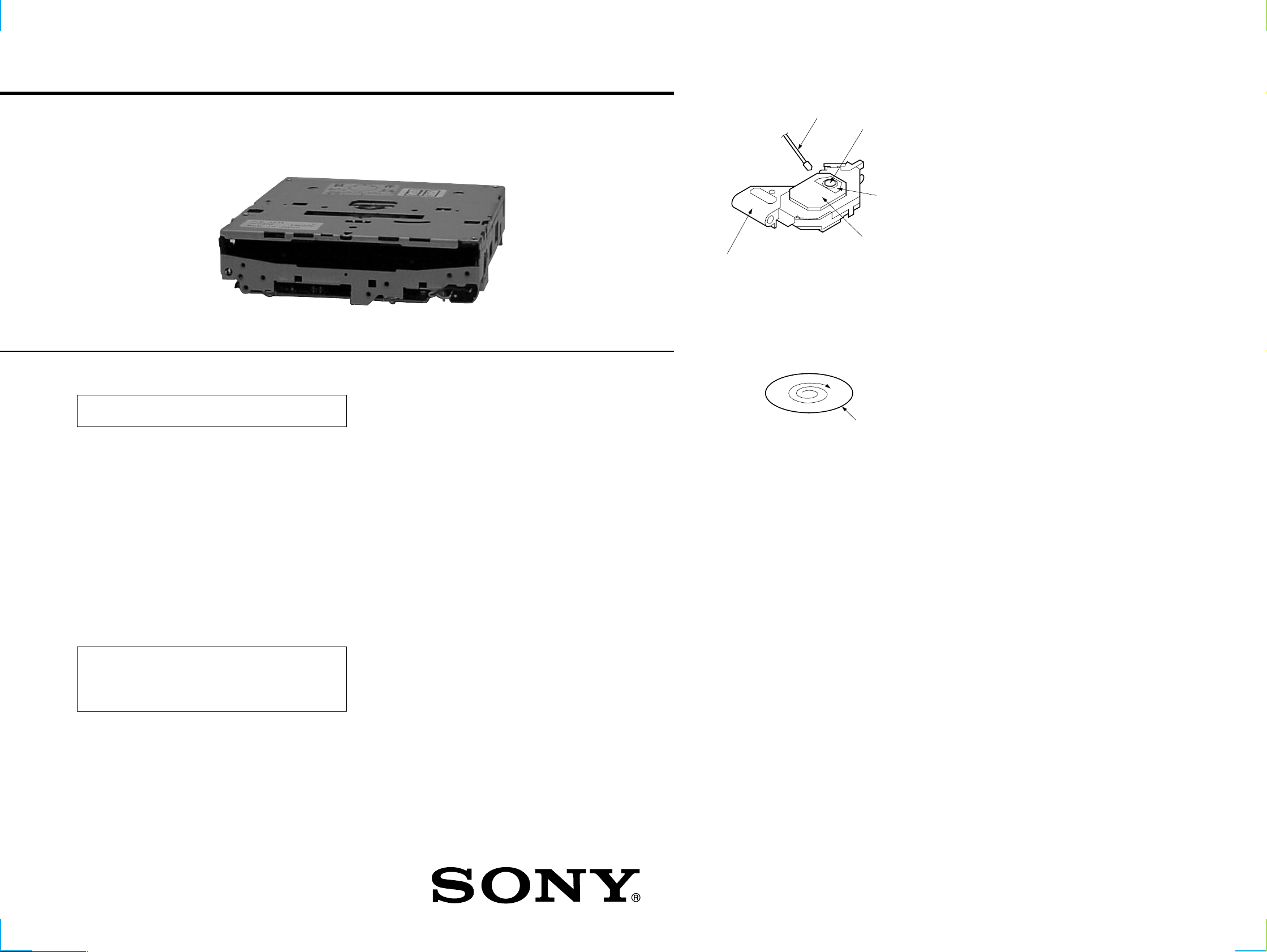
NOTES ON CLEANING THE OBJECTIVE LENS
SERVICE MANUAL
SERVICE NOTE
NOTES ON HANDLING THE OPTICAL PICK-UP BLOCK
OR BASE UNIT
The laser diode in the optical pick-up block may suffer electrostatic
breakdown because of the potential difference generated by the
charged electrostatic load, etc. on clothing and the human body.
During repair, pay attention to electrostatic breakdown and also use
the procedure in the printed matter which is included in the repair
parts.
The flexible board is easily damaged and should be handled with
care.
Laser Diode Properties
• Material: GaAlAs
• Wavelength: 780 nm
• Emission Duration: continuous
• Laser Output Power: less than 44.6 µW*
* This output is the v alue measured at a distance of 200 mm from
the objective lens surfase on the Optical Pick-up Block.
CAUTION
Use of controls or adjustments or performance of procedures
other than those specified herein may result in hazardous
radiation exposure.
Flexible Circuit Board Repairing
• Keep the temperature of the soldering iron around 270 °C
during repairing.
• Do not touch the soldering iron on the same conductor of the
circuit board (within 3 times).
• Be careful not to apply force on the conductor when soldering
or unsoldering
Notes on Chip Component Replacement
• Never reuse a disconnected chip component.
• Notice that the minus side of a tantalum capacitor may be
damaged by heat.
SAFETY-RELATED COMPONENT WARNING!!
COMPONENTS IDENTIFIED BY MARK 0 OR DOTTED LINE
WITH MARK 0 ON THE SCHEMATIC DIAGRAMS AND IN
THE PARTS LIST ARE CRITICAL TO SAFE OPERATION.
REPLACE THESE COMPONENTS WITH SONY PARTS WHOSE
P ART NUMBERS APPEAR AS SHOWN IN THIS MANU AL OR
IN SUPPLEMENTS PUBLISHED BY SONY.
cotton swabs
optical pick-up
slide base
Apply CD lens cleaner B-4 (Part No.:J-2501-000-A) to cotton swabs
(narrow type) (Part No.:J-2501-023-A) to be lightly wet. Use a force
(about 5 g (0.18 oz)) to make the objective lens in contact with the
bottom lightly, and clean the lens by spirals as following below.
Replace the cotton swab and repeat this cleaning two or three times.
surface of objective len
Notes:
Do not force to push the objective lens. Otherwise, the plate spring
supporting the objective lens will be bent, causing a deteriorated
RF waveform.
Never touch anything other than the objective lens. Otherwise, a
significant deterioration occurs in the RF waveform.
objective lens
2-axis actuato
2-axis cover
COMPACT DISC MECHANISM
SCD-333A
SECTION 1
DIAGRAMS
THIS NOTE IS COMMON FOR PRINTED WIRING
BOARDS AND SCHEMATIC DIAGRAMS.
for printed wiring boards:
• X : parts extracted from the component side.
• Y : parts extracted from the conductor side.
z
•
: Through hole.
• b : Pattern from the side which enables seeing.
(The other layer’s patterns are not indicated.)
Caution:
Pattern face side: Parts on the pattern face side seen from the
(Side B) pattern face are indicated.
Parts face side: Parts on the parts face side seen from the
(Side A) parts face are indicated.
for schematic diagram:
• All capacitors are in µF unless otherwise noted. pF: µµF
50 WV or less are not indicated except for electrolytics
and tantalums.
• All resistors are in Ω and 1/
specified.
4
W or less unless otherwise
• % : indicates tolerance.
f
•
: internal component.
Note: The components identified by mark 0 or dotted line
with mark 0 are critical for safety.
Replace only with part number specified.
• U : B+ Line.
• Signal path.
J : CD
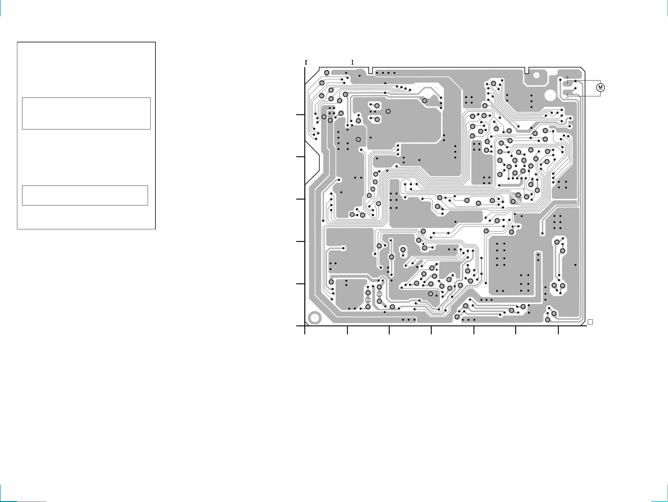
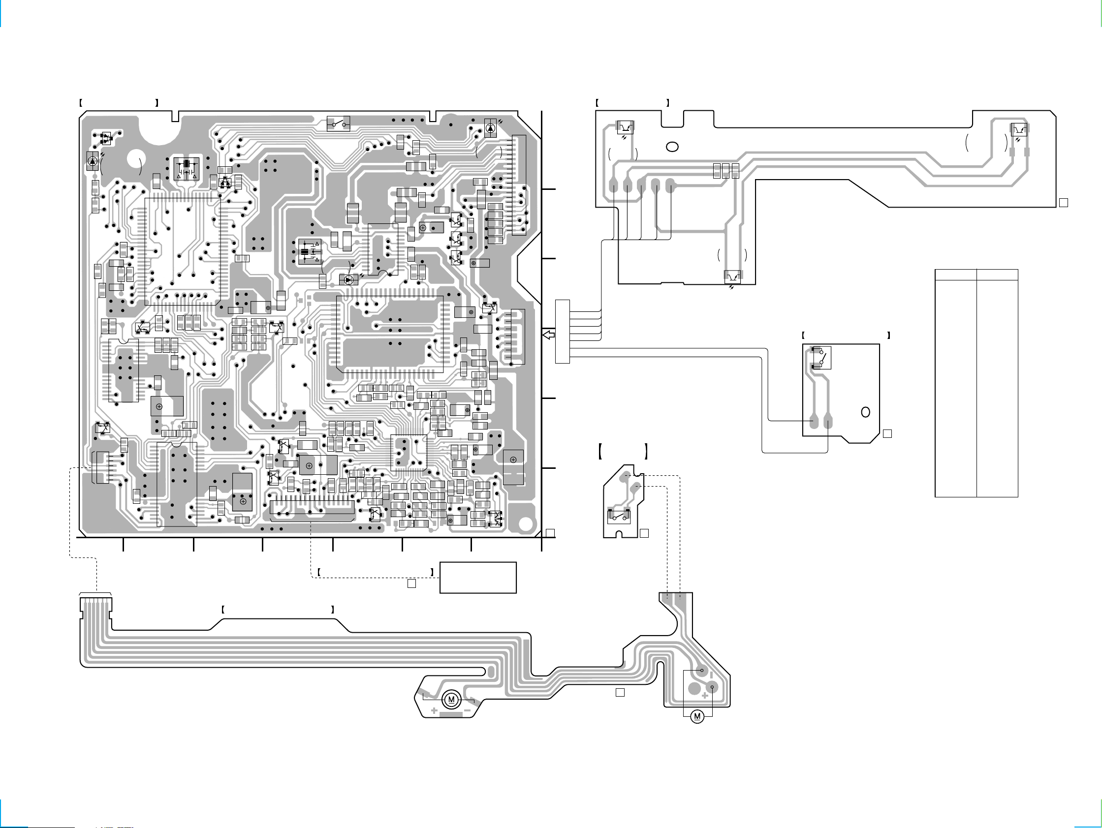
1-1. PRINTED WIRING BOARDS
MD-MAIN BOARD (SIDE A)
TP001
TP002
TP005
TP006
TP010
TP019
TP007
TP009
TP038 TP034
TP013
TP011
TP037
TP016
TP014
TP032
TP033
TP036
TP023
A
B
C
TP004
TP012
D
TP043
TP015
TP039
TP040
TP008
TP042
TP041
TP026
M70
M61
TP017
TP022
TP028
M24
M23
TP027
M25
M26
M16
M17
M02
TP003
TP025
M22
M06
M69
M15
M11
M07
M19
M39
M76
M75
TP029
M80
M29
M27
M63
M74
M67
M71
M21
M10
M28
M52
M35
M66
M41
M51
M58
M38
TP061
TP062
RED
WHT
M903
(LOADING)
TP066
TP069
TP068
TP065
TP073
TP067
TP070
TP050
TP071
TP055
TP049
TP072
TP054
TP051
TP056
TP057
TP063
TP059
TP064
TP058
1-660-771-
21
E
TP052
TP044
BR001
F
TP045
04
1
TP046
BR002
TP053
TP047
23 7456
2 2
SCD-333A
MD-MAIN BOARD (SIDE B)
D401
D632
LOADING
COMPLETION
DETECT
R632
R603
C621
R604
C620
R605
C403
125
IC402
13 14
Q401
CN104
1
6
R404
41 24
R607
R620
R621
64
65
Q603
R408
R406
X601
C630
IC601
R610
R612
R407C405
R405
R403
C404
C411
R590
R606R402
1
IC401
14 15
R609
28
2540
80
R611
R602
C627
D601
1
C402
C602
R401
R608
R550
C591
C590
R593
C401
R601
C410
SW602
(CHAKING DET)
C210
X301
C610
R591
R592
R594
R595
L601
Q590
R548
C532
Q502
L503
R511
R512
R546
Q501
116
C554
R502
C303
L301
D631
DISC IN
DETECT
R631
52
64
119
R536
C524
C507
C505
C504
R510
C506
R508
R509
R503
R507
R504
R501
R506
R544
CN103
13 12
IC301
24 1
IC502
R535
R537
C503
25
36
R505
R547
C530
Q504
C525
R534
R543
C508
R545
R513
C509
R514C512
C601
L101
C110
IC501
L201
C302C304
C526
C523
R518
C510
R541
R515
R630
R301
R533
1324
4837
C101
C310
C305
3351
12
1
C201
C301
Q302
Q602
32
20
R532
R530
R531
R529
C513
C511
R517
R542
237456
R528
C521
Q301
C556
C518
R524
C514
R520
C553
C501
R525
R539
R540
C519
R526
C515
C628
C629
C611
L501
C528
C529
C527
R538
R527
C520
C516
R523
C517
R519
R522
R521
D630
DISC IN
DETECT
L602
C626
C625
C624
C623
C622
Q601
C522
C502
C555
L502
Q503
1-660-771-
1
CN101
20
10
1
CN102
7
1
C552
A
B
C
D
E
F
SENSOR BOARD
Q623
LOADING
Q620
DISC IN
DETECT
R620
R622
R621
BLK/WHT
ORG/WHT
BLU/WHT
WHT
PNK/WHT
Q621
7
PNK/WHT
WHT
BLU/WHT
ORG/WHT
BLK/WHT
RED
BLK
1
DISC IN
DETECT
DISC IN SW BOARD
SW621
(DISC IN)
1-660-773-
13
• Semiconductor
LIMIT SW
BOARD
SW620
(LIMIT)
21
1-660-772-
13
COMPLETION
DETECT
Location
Ref. No. Location
D401 A-7
D601 A-5
D630 A-1
D631 C-3
D632 A-7
IC301 B-3
IC401 F-6
IC402 D-7
IC501 E-2
IC502 D-3
IC601 B-6
Q301 B-2
Q302 B-2
Q401 E-7
Q501 F-4
Q502 E-4
Q503 F-1
Q504 F-3
Q590 C-4
Q601 C-1
Q602 B-2
Q603 C-6
1-660-775-
13
61
04
MOTOR FLEXIBLE BOARD
PICK-UP FLEXIBLE BOARD
1-660-769-
11
M902
(SLED)
OPTICAL
PICK-UP
KSS-520A
1-660-770-
11
33
M901
(SPINDLE)
 Loading...