

Sony SAWVS-200 Service manual
SA-WVS200/WVS300
SERVICE MANUAL
Ver 1.0 2004. 07
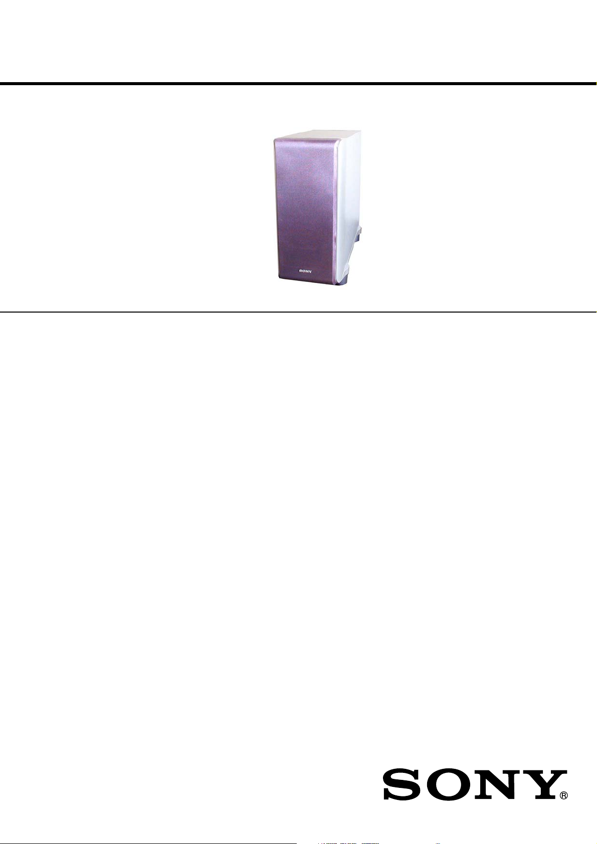
Photo: SA-WVS300
• SA-WVS200 is active subwoofer in SA-VS200H
• SA-WVS300 is active subwoofer in SA-VS300H
SPECIFICATIONS
US Model
Canadian Model
SA-WVS300
AEP Model
SA-WVS200/WVS300
UK Model
E Model
SA-WVS300
Chinese Model
SA-WVS200
SA-WVS300
AUDIO POWER SPECIFICATIONS
(For the U.S. model)
POWER OUTPUT AND TOTAL HARMONIC DISTORTION:
with 6 ohm loads both channels driven, at 100 Hz; rated 150
watts per channel minimum RMS power, with no more than
10% total harmonic distortion from 250 milliwatts to rated
output.
SA-WVS200/WVS300
Speaker system Active subwoofer,
magnetically shielded
Speaker units Woofer: 15 cm (6 in.) (x 2), cone type
Enclosure type Acoustically Loaded Bass reflex
Reproduction frequency range
28 Hz - 200 Hz
Continuous RMS power output
150 W (6 ohms 100 Hz, 10% THD)
Input
LINE IN (input pin jack)
General
Power requirements 120 V AC, 60 Hz (US, Canadian model)
220 - 230 V AC, 50/60 Hz
(EXCEPT US, Canadian model)
Power consumptions 90 W
1 W (standby mode)
Dimensions (w/h/d) Approx. 197 x 407 x 502 mm
(7 7/8 x 16 1/8 x 19 7/8 in.),
including front grille
Mass Approx. 12.2 kg
(26 lb 15 oz)
Design and specifi cations are subject to change without notice.
9-879-064-01
2004G02-1
© 2004.07
ACTIVE SUBWOOFER
Sony Corporation
Home Audio Company
Published by Sony Engineering Corporation
SA-WVS200/WVS300
SAFETY CHECK-OUT
After correcting the original service problem, perform the following
safety checks before releasing the set to the customer:
Check the antenna terminals, metal trim, “metallized” knobs, screws,
and all other exposed metal parts for AC leakage. Check leakage as
described below.
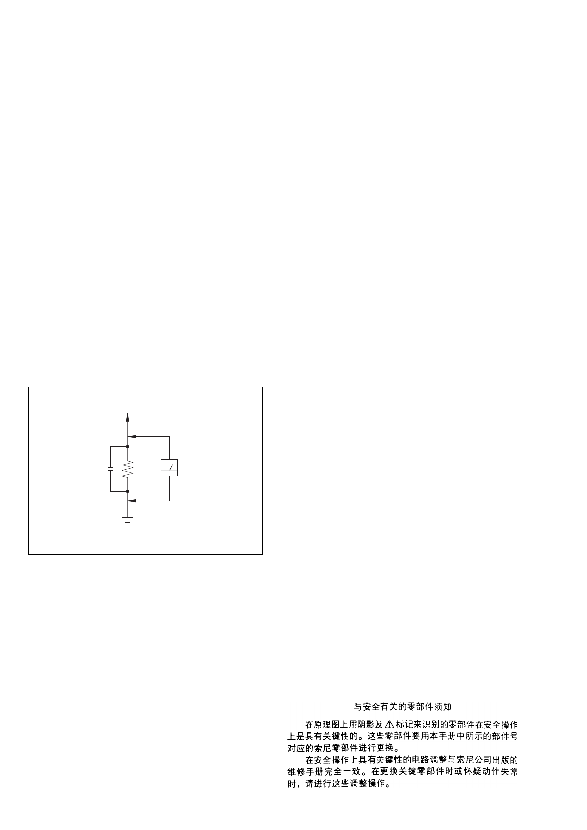
LEAKAGE
The AC leakage from any exposed metal part to earth ground and
from all exposed metal parts to any exposed metal part having a
return to chassis, must not exceed 0.5 mA (500 microamperes).
Leakage current can be measured by any one of three methods.
1. A commercial leakage tester, such as the Simpson 229 or RCA
WT-540A. Follow the manufacturers’ instructions to use these
instruments.
2. A battery-operated AC milliammeter. The Data Precision 245
digital multimeter is suitable for this job.
3. Measuring the voltage drop across a resistor by means of a
VOM or battery-operated AC voltmeter. The “limit” indication
is 0.75 V, so analog meters must have an accurate low-voltage
scale. The Simpson 250 and Sanwa SH-63Trd are examples
of a passive VOM that is suitable. Nearly all battery operated
digital multimeters that have a 2V AC range are suitable. (See
Fig. A)
TABLE OF CONTENTS
1. DIAGRAMS
1-1. Printed Wiring Boards– Pri Amp Section –..................... 3
1-2. Schematic Diagram – Pri Amp Section – ........................ 4
1-3. Printed Wiring Boards – Power Amp Section– ............... 5
1-4. Schematic Diagram – Power Amp Section – .................. 6
2. EXPLODED VIEWS
2-1. Main Section.................................................................... 7
3. ELECTRICAL PARTS LIST .................................. 8
To Exposed Metal
Par ts on Set
AC
0.15 µF
Fig. A. Using an AC voltmeter to check AC leakage.
1.5 kΩ
Earth Ground
Voltmeter
(0.75 V)
SAFETY-RELATED COMPONENT WARNING!!
COMPONENTS IDENTIFIED BY MARK 0 OR DOTTED LINE WITH
MARK 0 ON THE SCHEMATIC DIAGRAMS AND IN THE PARTS
LIST ARE CRITICAL TO SAFE OPERATION. REPLACE THESE
COMPONENTS WITH SONY PARTS WHOSE PART NUMBERS
APPEAR AS SHOWN IN THIS MANUAL OR IN SUPPLEMENTS
PUBLISHED BY SONY.
ATTENTION AU COMPOSANT AYANT RAPPORT
À LA SÉCURITÉ!
LES COMPOSANTS IDENTIFÉS PAR UNE MARQUE 0 SUR LES
DIAGRAMMES SCHÉMATIQUES ET LA LISTE DES PIÈCES SONT
CRITIQUES POUR LA SÉCURITÉ DE FONCTIONNEMENT. NE
REMPLACER CES COMPOSANTS QUE PAR DES PIÈSES SONY
DONT LES NUMÉROS SONT DONNÉS DANS CE MANUEL OU
DANS LES SUPPÉMENTS PUBLIÉS PAR SONY.
2
SECTION 1
DIAGRAMS
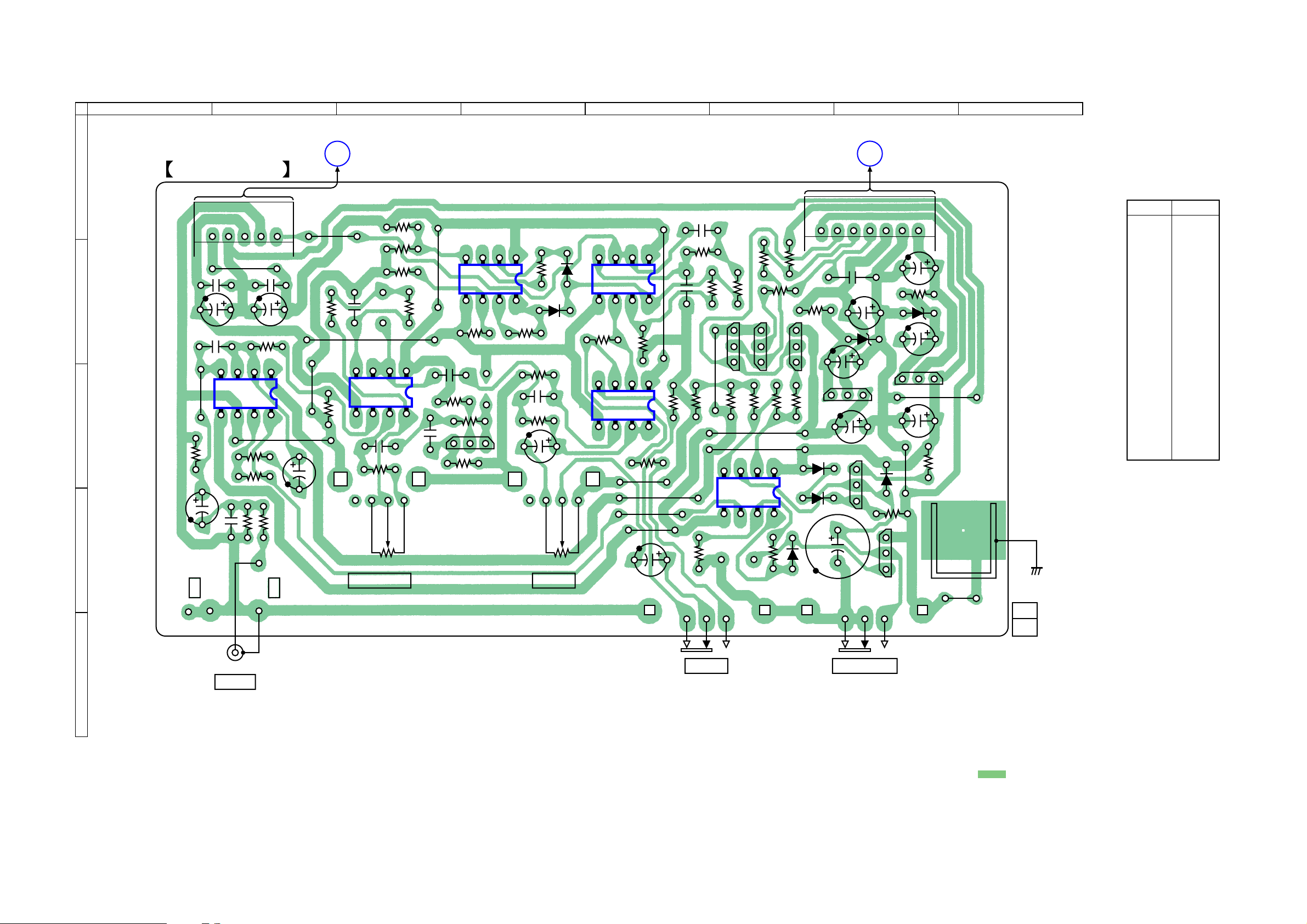
1-1. PRINTED WIRING BOARD – PRI AMP SECTION –
SA-WVS200/WVS300
1
2
POWER AMP BOARD
A
A
B
C
D
PRI AMP BOARD
BC506
15
JW501
C515 C514
C516C517
IC501
R502
R501C501
R504
85
14
JW504
C519
JW502
R503
C502
C503
R511
R512
JW504
R506
JW505
R529
R530
R526
JW504
R531
IC503
3 4 5 6 7
(Page 5)
JW507
R528
85
IC506
14
C506
C504
R505
VR501 VR502
R515
C508
85
R507
14
B
C505
R509
1414
R527R525
R508
E
Q501
R516
C509
R517
LEVELBASS BOOST
D501
C510
D502
R520
IC505
IC504
JW508
C511
85
14
R521
85
14
R519
JW509
JW510
JW511
JW512
R518
C512
R405
JW513
R513
C513
R524
R522
E
B
IC502
R523
E
Q404
B
R403
JW516
JW518
R408
R410
Q405
R404
85
14
R514
E
B
R406
R409
R807
D815
Q403
B
R407
C821
D402
D403
C402
D404
C520
Q804
E
B
AUTO POWER BOARD
B
BC504
C817
C819
E
Q402
S401S501
B
D401
R402
E
B
Q803
Q401
(Page 5)
17
C816
R806
D814
C818
E
JW515
C820
R401
JW517
JW519
1-863-035-
8
• Semiconductor
Location
Ref. No. Location
D401 C-7
D402 C-6
D403 D-6
D404 D-6
D501 B-4
D502 B-4
D814 B-7
D815 B-7
IC501 C-2
IC502 D-6
IC503 C-3
IC504 C-5
IC505 B-5
IC506 B-4
Q401 D-7
Q402 D-7
Q403 B-6
Q404 B-6
Q405 B-6
Q501 C-4
Q803 C-7
Q804 C-7
(CHASSIS)
11
(11)
E
SA-WVS200/WVS300
J501
LINE IN
PHASE
POWER SAVE
AUTOtOFFNORMALtREVERSE
For printed wiring boards.
Note:
• X : parts extracted from the component side.
• : Pattern from the side which enables seeing.
33

SA-WVS200/WVS300
1-2. SCHEMATIC DIAGRAM – PRI AMP SECTION –
J501
1P
LINE IN
R501
1k
R502
100k
C503
220p
C502
50V
C501
220p
10
C519
50V
C817
50V
10
C514
0.1
7
IC505(2/2)
BA4558
C816
C512
0.056
10
50V
C516
10
50V
IC504(1/2)
BA4558
HPF
LPF
10
IC504(2/2)
BA4558
PHASE SWITCH
S501
PHASE
NORMAL
REVERSE
R518
10k
R519
10k
Q404
DTA124ES
LED DRIVER
5
6
R408
R409
2.2k
IC505(1/2)
BA4558
8
7
R520
10k
R521
1k
1k
3
2
R529
15k
R530
2.7k
R522
15k
4
1
8
6
5
IC506(2/2)
BA4558
Q405
DTA124ES
LED DRIVER
R410
2.2k
R528
10k
7
LIMITTER
IC501(2/2)
BA4558
BUFFER
7
IC501(1/2)
BA4558
AMP
R512
470k
2
4
3
R504
10k
R531
6.8k
1
R513
2.2k
6
8
5
R503
100k
10
R511
2.2k
2
3
R505
1k
C504
0.22
C505
0.22
R508
3.3k
IC502(1/2)
BA4558
AMP
R514
15k
2
4
3
IC503(1/2)
BA4558
4
1
VR501
5KB
R509
39k
1SS133
1SS133
1
Q401,402
AUDIO LEVEL
DETECT
D401
D404
R506
BASS
BOOST
Q501
2SC2785
Q401
DTC124ES
C510
50V
1
VR502
20KB
LEVEL
IC502(2/2)
BA4558
AUTO POWER
CONTROL
R406
1M
5
6
8
10
7
DTC124ES
RELAY DRIVE
C511
R407
Q403
S401
50V
10k
C508
0.22
R402
10k
R405
10k
R517
4.7k
C509
0.22
R403
10k
2
3
R516
68k
R404
100k
4
Q402
2SA1175
8
6
5
IC503(2/2)
BA4558
C506
0.047
C402
330
16V
7
D402
1SS133
D403
1SS133
R515
10k
0
R507
1k
R401
100k
D502
1SS133
D501
1SS133
C820
25V
C821
25V
LPF
C513
0.22
R523
8.2k
R524
8.2k
4
3
1
2
R527
10k
IC506(1/2)
BA4558
Q803
2SC1815
+12V REG
47
47
Q804
2SA1015
-12V REG
C818
10
50V
C819
10
50V
6
5
R525
R526
2.7k
R806
3.3k
D814
MTZJ-13B
D815
MTZJ-13B
R807
3.3k
8
15k
C520
0.1
C515
0.1
C517
10
50V
BC506
BC504
POWER AMP
BOARD
(Page6)
7P
AUTO POWER
BOARD
(Page6)
SA-WVS200/WVS300
For schematic diagrams.
• All capacitors are in µF unless otherwise noted. pF: µµF
50 WV or less are not indicated except for electrolytics
and tantalums.
• All resistors are in Ω and 1/
specified.
4
W or less unless otherwise
• 2 : nonflammable resistor.
• 5 : fusible resistor.
• C : panel designation.
Note:
The components identified by mark 0 or dotted
line with mark 0 are critical for safety.
Replace only with part
number specified.
Note:
Les composants identifiés par
une marque 0 sont critiques
pour la sécurité.
Ne les remplacer que par une
piéce portant le numéro
spécifié.
44
• A : B+ Line.
• B : B– Line.
•Voltages and waveforms are dc with respect to ground
under no-signal (detuned) conditions.
•Voltages are taken with a VOM (Input impedance 10 MΩ).
Voltage variations may be noted due to normal production tolerances.
• Signal path.
F : AUDIO
• Abbreviation
CND : Canadian model
SP : Singapore model
CH : Chinese model
KR : Korea model
 Loading...