Sony SAWSLF-1 Service manual
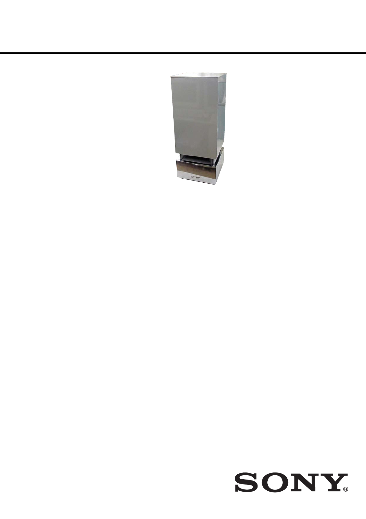
SA-WSLF1
SERVICE MANUAL
Ver 1.0 2004.08
• SA-WSLF1 is amplifier/subwoofer and tuner
system in DAV-LF1.
SPECIFICATIONS
AUDIO POWER SPECIFICATIONS
POWER OUTPUT AND
TOTAL HARMONIC
DISTORTION: With 4 ohm loads, both
Amplifier section
Stereo mode (rated) 86 W + 86 W (4 ohms at
Surround mode Front: 86 W (each)
(reference) (with SS-TSLF1)
music power output Center*:
*Depending on the sound field settings and the source,
there may be no sound output.
Inputs VIDEO/TV/SAT:
Phones Accepts low-and high-
channels driven, from
200 – 20,000 Hz; rated
65 watts per channel
minimum RMS power,
with no more than 0.7 %
total harmonic distortion
from 250 milli watts to
rated output.
1 kHz, THD 10 %)
86
(with SS-CTLF1)
Surround (R)*:
(with SS-TSLF1W)
Surround (L):
(with SA-TSLF1)
Subwoofer*:
(with SA-WSLF1)
Sensitivity: 300 mV
Impedance: 50 kilohms
impedance headphones.
W
86
85
86
W
W
W × 2
Tuner section
System PLL quartz-locked digital
FM tuner section
Tuning range 87.5 – 108.0 MHz (50 kHz
Antenna (aerial) FM wire antenna ( aerial)
Antenna (aerial) terminals
Intermediate frequency 10.7 MHz
AM tuner section
Tuning range
Middle Easten models: 531 – 1, 602 kHz (with the
Other models: 531 – 1,602 kHz (with the
Antenna (aerial) AM loop antenna (aerial)
Intermediate frequency 450 kHz
Video section
Outputs Video: Vp-p 75 ohms
Inputs
synthesizer system
step)
75 ohms, unbalanced
interval set at 9 kHz)
interval set at 9 kHz)
530 – 1,710 kHz (with the
interval set at 10 kHz)
S video:
Y: 1 Vp-p 75 ohms
C: 0.286 Vp-p 75 ohms
COMPONENT:
Y: 1 Vp-p 75 ohms
P
B/CB
75 ohms
Video: 1 Vp-p 75 ohms
, PR/CR: 0.7 Vp-p
US Model
Canadian Model
AEP Model
UK Model
E Model
Subwoofer
Speaker system Bass reflex
Speaker unit 180 mm (7
dia. cone type
Rated impedance 4 ohms × 2
Dimensions (approx.) 241 × 606 × 241 mm
(9
inches) (w/h/d)
Mass (approx.) 14 kg (30 lb 14 oz)
Power requirements
North American and
Mexican models: 120 V AC, 60 Hz
Taiwan model: 120 V AC, 50/60 Hz
Other models: 220-240 V AC, 50/60 Hz
Power consumption 120 W
0.3 W (a t the Power
Saving mode)
Design and specifications are subject to change
without notice.
1
/8 inches)
1
/2 × 23 7/8 9 ×1/2
9-879-144-01
2004H1678-1
© 2004.08
ACTIVE SUBWOOFER
Sony Corporation
Audio Group
Published by Sony Engineering Corporation
SA-WSLF1
r
Notes on chip component replacement
• Never reuse a disconnected chip component.
• Notice that the minus side of a tantalum capacitor may be
damaged by heat.
Flexible Circuit Board Repairing
• Keep the temperature of the soldering iron around 270 °C
during repairing.
• Do not touch the soldering iron on the same conductor of the
circuit board (within 3 times).
• Be careful not to apply force on the conductor when soldering
or unsoldering.
UNLEADED SOLDER
Boards requiring use of unleaded solder are printed with the leadfree mark (LF) indicating the solder contains no lead.
(Caution: Some printed circuit boards may not come printed with
the lead free mark due to their particular size)
: LEAD FREE MARK
Unleaded solder has the following characteristics.
• Unleaded solder melts at a temperature about 40 °C higher
than ordinary solder.
Ordinary soldering irons can be used but the iron tip has to be
applied to the solder joint for a slightly longer time.
Soldering irons using a temperature regulator should be set to
about 350 °C.
Caution: The printed pattern (copper foil) may peel away if
the heated tip is applied for too long, so be careful!
• Strong viscosity
Unleaded solder is more viscou-s (sticky, less prone to flow)
than ordinary solder so use caution not to let solder bridges
occur such as on IC pins, etc.
• Usable with ordinary solder
It is best to use only unleaded solder but unleaded solder may
also be added to ordinary solder.
SAFETY CHECK-OUT
After correcting the original service problem, perform the following
safety check before releasing the set to the customer:
Check the antenna terminals, metal trim, “metallized” knobs, screws,
and all other exposed metal parts for AC leakage.
Check leakage as described below.
LEAKAGE TEST
The AC leakage from any exposed metal part to earth ground and
from all exposed metal parts to any exposed metal part having a
return to chassis, must not exceed 0.5 mA (500 microamperes.).
Leakage current can be measured by any one of three methods.
1. A commercial leakage tester, such as the Simpson 229 or RCA
WT -540A. Follow the manuf acturers’ instructions to use these
instruments.
2. A battery-operated A C milliammeter . The Data Precision 245
digital multimeter is suitable for this job.
3. Measuring the voltage drop across a resistor by means of a
VOM or battery-operated AC v oltmeter. The “limit” indication
is 0.75 V, so analog meters must have an accurate lo w-voltage
scale. The Simpson 250 and Sanwa SH-63Trd are examples
of a passive VOM that is suitable. Nearly all battery operated
digital multimeters that have a 2 V A C range are suitable. (See
Fig. A)
To Exposed Metal
Parts on Set
AC
0.15 µF
1.5 k
Ω
voltmete
(0.75 V)
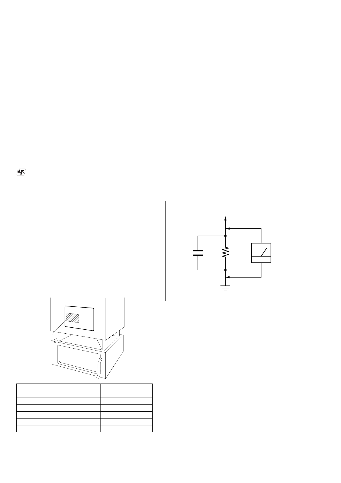
MODEL IDENTIFICATION
– Rear Side –
Part No.
Model Name Part No.
AEP, UK, Russian models 2-318-584-0[]
US, CND models 2-320-434-0[]
EA, E41 models 2-320-799-0[]
MX model 2-320-800-0[]
KR model 2-320-801-0[]
SP, HK models
•Abbreviation
CND : Canadian model.
E41 : Chilean and peruvian models.
EA : Saudi Arabia model.
HK : Hong Kong model.
KR : Korea model.
MX : Mexican model.
RU : Russian model.
SP : Singapore model.
Earth Ground
Fig. A. Using an AC voltmeter to check AC leakage.
SAFETY-RELATED COMPONENT WARNING!!
COMPONENTS IDENTIFIED BY MARK 0 OR DOTTED LINE
WITH MARK 0 ON THE SCHEMATIC DIAGRAMS AND IN
THE PARTS LIST ARE CRITICAL TO SAFE OPERATION.
REPLACE THESE COMPONENTS WITH SONY PARTS WHOSE
PART NUMBERS APPEAR AS SHOWN IN THIS MANUAL OR
IN SUPPLEMENTS PUBLISHED BY SONY.
ATTENTION AU COMPOSANT AYANT RAPPORT
À LA SÉCURITÉ!
LES COMPOSANTS IDENTIFIÉS PAR UNE MARQUE 0 SUR
LES DIAGRAMMES SCHÉMATIQUES ET LA LISTE DES
PIÈCES SONT CRITIQUES POUR LA SÉCURITÉ DE
FONCTIONNEMENT. NE REMPLACER CES COM- POSANTS
QUE PAR DES PIÈCES SONY DONT LES NUMÉROS SONT
DONNÉS DANS CE MANUEL OU D ANS LES SUPPLÉMENTS
PUBLIÉS PAR SONY.
2

TABLE OF CONTENTS
SA-WSLF1
1. SERVICING NOTES ................................................ 4
2. GENERAL ................................................................... 6
3. ELECTRICAL ADJUSTMENTS .......................... 7
4. DIAGRAMS
4-1. Block Diagram — AMP (DSP) Section — .................. 9
— AUDIO (OUT) Section — .......................................... 10
— VIDEO Section —...................................................... 11
— DIAT TRANSMITTER Section — ............................ 12
4-2. Printed W iring Board
— JACK COMB Section (Side A) — ............................. 13
4-3. Printed W iring Board
— JACK COMB Section (Side B) — ............................. 14
4-4. Schematic Diagram — JACK COMB Section — .......... 15
4-5. Printed W iring Board
— SW-MAIN Section (Side A) — .................................. 16
4-6. Printed W iring Board
— SW-MAIN Section (Side B) —.................................. 17
4-8. Schematic Diagram — SW-MAIN Section (1/4) —...... 18
4-9. Schematic Diagram — SW-MAIN Section (2/4) —...... 19
4-10. Schematic Diagram — SW-MAIN Section (3/4) —...... 20
4-11. Schematic Diagram — SW-MAIN Section (4/4) —...... 21
4-12. Printed Wiring Board — AMP Section (Side A) —....... 22
4-13. Printed Wiring Board — AMP Section (Side B) — ....... 23
4-14. Schematic Diagram — AMP Section (1/4) — ............... 24
4-15. Schematic Diagram — AMP Section (2/4) — ............... 25
4-16. Schematic Diagram — AMP Section (3/4) — ............... 26
4-17. Schematic Diagram — AMP Section (4/4) — ............... 27
4-18. Printed Wiring Board
— DIAT TRANSMITTER Section — ............................ 28
4-19. Schematic Diagram
— DIAT TRANSMITTER Section — ............................ 29
4-20. Printed Wiring Board — POWER Section — ................ 30
4-21. Schematic Diagram — POWER Section — .................. 31
5. EXPLODED VIEWS
5-1. AMP Section-1................................................................ 42
5-2. AMP Section-2................................................................ 43
5-3. Overall Section................................................................ 44
6. ELECTRICAL PARTS LIST .................................. 45
3
SA-WSLF1
SECTION 1
SERVICING NOTES
• The units that are required for the system operation check during repair service
Unit.
need to
checking
Units required for
operation
check
DVD player :
HCD-LF1
Sub woofer :
SA-WSLF1
Front speaker :
SS-TSLF1(R)
SS-TSLF1L(L)
Center speaker :
SS-CTLF1
Surround speaker :
SS-TSLF1W(R)
SA-TSLF1(L)
Remote
commander :
RM-SP320
DVD player : HCD-LF1
Sub woofer : SA-WSLF1
Front speaker : SS-TSLF1(R)
SS-TSLF1L(L)
Center speaker :
SS-CTLF1
Surround speaker : SS-TSLF1W(R)
SA-TSLF1(L)
Remote commander :
RM-SP320
*1 Only the defective unit. *2 Either one of them.
Units with a mark: The units that are required for the system operation check during repair service
However, there can be a case that some units of the system need to not be brought into repair shop depending on the unit. that became defective.
aa a
aa a
aaa
aaa a
*1
*2
a
a
*1
a
a
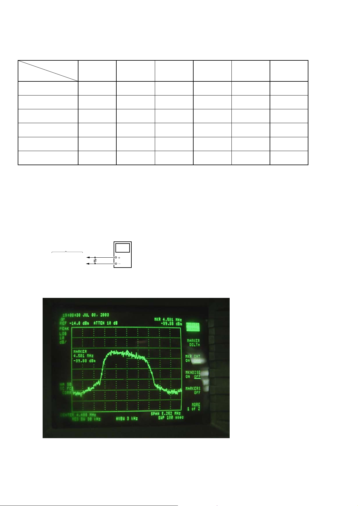
[The check method of the output signal from DIAT TRANSMITTER board]
Procedure:
1. A spectrum analyzer is connected to pin 2 and pin 1 of the output connector CN803 of DIAT TRANSMITTER board.
digital
DIAT TRANSMITTER
board
10 Ω(0.5%)
CN803 Pin 1
Pin 2
voltmeter
2. Confirm that it is spectrum as shown in a figure with the spectr um analyzer . It is normal if the signal of a 3MHz to 6MHz zone (a center
is 4.5MHz) can be checked.
3. When the output signal from DIAT TRANSMITTER board is normal, pin 8 (SDATA), pin 4 (LRCKO) and pin 5 (BCKO) of the input
signal connector CN801 are investigated.
4
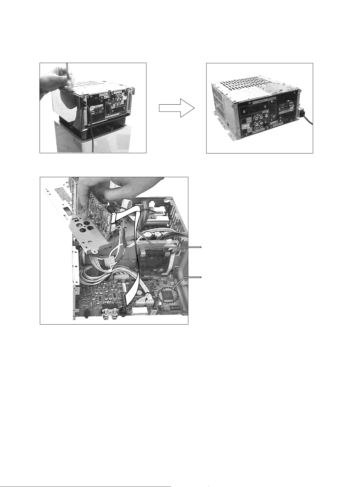
•NOTE:
Turn the woofer upside down and remove the AMP block.
• SERVICING POSITION (SW-MAIN Board)
SA-WSLF1
Connect the SW-MAIN board and the VIDEO-I/O board
using the extension cable and check the SW-MAIN board.
•CAUTION:
Keep your eyes 10 cm or more away from the infrared laser unit (DIR-T1).
Do not view directly the laser beam.
J-2501-245-A
(1mm/23P/L300)
IC525 on the SW-MAIN board
5
SA-WSLF1
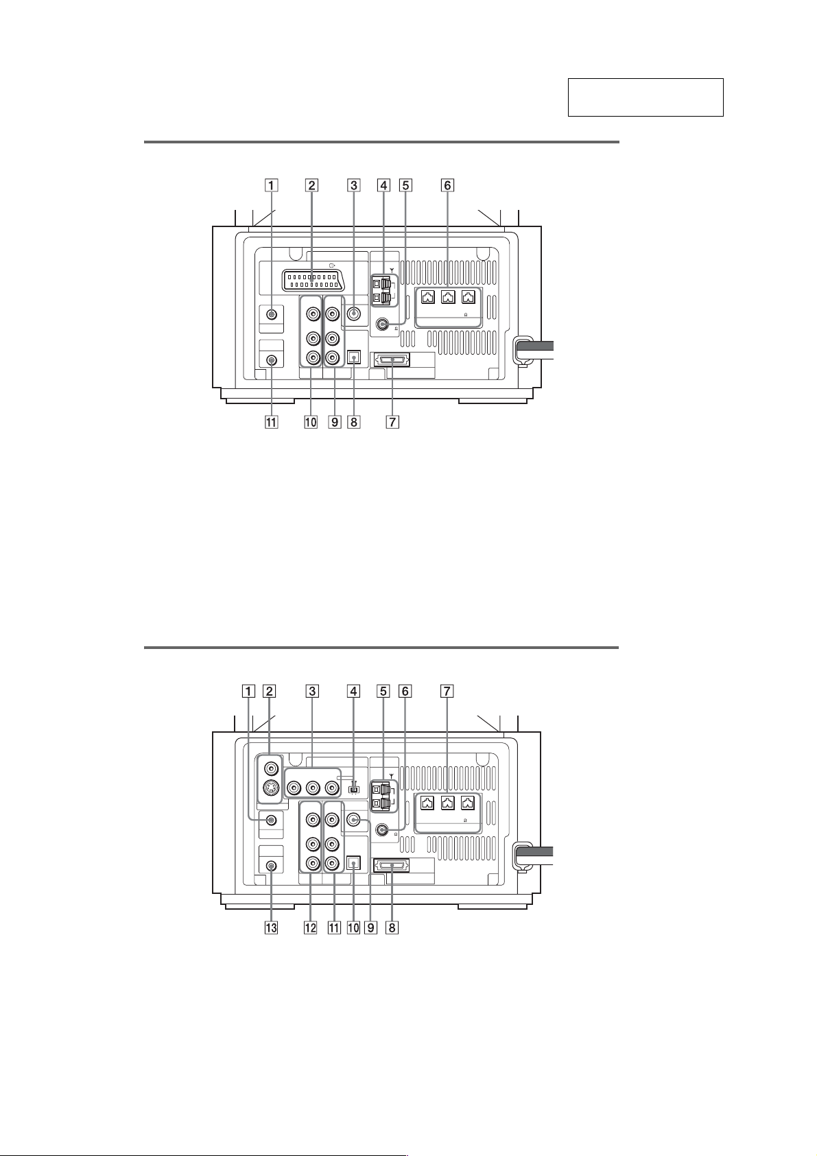
(AEP, UK, Russian models)
Subwoofer (Rear Panel)
OUTPUT(TO TV)
SECTION 2
GENERAL
This section is extracted
from instruction manual.
EURO AV ANTENNA
A PHONES jack (39)
B EURO AV OUTPUT (TO TV) T jacks
(25)
C DIR-T1 jack (18)
D AM terminals (23)
E FM 75Ω COAXIAL jack (23)
F SPEAKER jacks (18)
(EXCEPT AEP, UK, Russian models)
Subwoofer (Rear Panel)
PHONES
REMOTE
CONTROL
VIDEO
VIDEO DIR-T1
IN
IN
AUDIO
AUDIO
IN
IN
OPTICAL
LL
R
VIDEO
DIGITAL IN
R
SAT
AM
CENTER FRONT L
FRONT R
IMPEDANCE USE 4
FM
75
COAXIAL
SYSYTEM CONNECTOR
SPEAKER
G SYSTEM CONNECTOR jack (15)
H SAT OPTICAL DIGITAL IN jack (26)
I SAT (VIDEO IN/AUDIO IN (L/R)) jacks
(25)
J VIDEO (VIDEO IN/AUDIO IN (L/R)) jacks
(25)
K REMOTE CONTROL jack (18)
VIDEO
S VIDEO (DVD ONLY)
MONITOR OUTPUT
PHONES
REMOTE
CONTROL
A PHONES jack (41)
B MONITOR OUTPUT (VIDEO/S VIDEO)
jacks (25)
C COMPONENT VIDEO OUT jacks (25)
D COMPONENT VIDEO OUT/SCAN
SELECT switch (88)
E AM terminals (23)
F FM 75Ω COAXIAL jack (23)
COMPONENT VIDEO OUT ANTENNA
PB/CBPR/CRSCAN SELECT
Y
VIDEO
VIDEO DIR-T1
IN
IN
AUDIO
AUDIO
IN
IN
OPTICAL
LL
R
VIDEO
DIGITAL IN
R
SAT
INTERLACESELECTABLE
AM
CENTER FRONT L
FRONT R
IMPEDANCE USE 4
FM
75
COAXIAL
SYSYTEM CONNECTOR
SPEAKER
H SYSTEM CONNECTOR jack (15)
I DIR-T1 jack (18)
J SAT OPTICAL DIGITAL IN jack (26)
K SAT (VIDEO IN/AUDIO IN (L/R)) jacks
(25)
L VIDEO (VIDEO IN/AUDIO IN (L/R)) jacks
(25)
M REMOTE CONTROL jack (18)
G SPEAKER jacks (18)
6

SECTION 3
p
ELECTRICAL ADJUSTMENT
DIAT SIGNAL RF LEVEL ADJUSTMENT
This adjustment is performed in order to adjust the transmission
distance of RF signal for DIAT communication.
Connection:
SA-WSLF1
DIA T TRANSMITTER
board
TP815
(RF AMP OUT)
Procedure:
1. Connect the oscilloscope to TP815 (RF AMP OUT) and GND
on the DIAT TRANSMITTER board.
2. Connect DIR-T1 to DIR-T1 jack (J908).
3. Adjust RV801 on the DIAT TRANSMITTER board so that
the center of waveform becomes Trig level 1.05 Vp-p.
(*Trigger position: –4 div)
4. Confirm trigger is locked.
5. Adjust RV801 on the DIAT TRANSMITTER board so that
the center of waveform becomes 2.2 to 2.4 Vp-p.
oscilloscope
VOLT/DIV : 500 mV
TIME/DIV : 500 ns
level : 2.2 to 2.4 Vp-
RF Signal Reference Waveform
Adjustment Location:
– DIAT TRANSMITTER Board (SIDE A) –
IC804
IC805
TP815
(RF AMP OUT)
7
SA-WSLF1
SECTION 4
DIAGRAMS
THIS NOTE IS COMMON FOR PRINTED WIRING BOARDS AND SCHEMATIC DIAGRAMS.
(In addition to this, the necessary note is printed in each block.)
For Schematic Diagrams.
Note:
• All capacitors are in µF unless otherwise noted. (p: pF)
50 WV or less are not indicated except f or electrolytics and
tantalums.
• All resistors are in Ω and 1/
specified.
• f : internal component.
• C : panel designation.
Note:
The components identified by mark 0 or dotted
line with mark 0 are critical for safety.
Replace only with part
number specified.
• A : B+ Line.
•Voltages and wavef orms are dc with respect to ground under no-signal (detuned) conditions.
no mark : DVD STOP
•Voltages are taken with a VOM (Input impedance 10 MΩ).
Voltage v ariations ma y be noted due to normal production
tolerances.
•Waveforms are taken with a oscilloscope.
Voltage v ariations ma y be noted due to normal production
tolerances.
• Circled numbers refer to waveforms.
• Signal path.
F : AUDIO
d : TUNER
J : CD PLAY
c : DVD PLAY
L : VIDEO
E : Y
a : CHROMA
r : COMPONENT VIDEO
q : R, G, B
e : AUX IN (AUDIO)
h : DIGITAL IN
i : AUX IN (VIDEO)
4
W or less unless otherwise
Note:
Les composants identifiés par
une marque 0 sont critiques
pour la sécurité.
Ne les remplacer que par une
piéce portant le numéro
spécifié.
For Printed Wiring Boards.
Note:
• X : parts extracted from the component side.
• a : Through hole.
• : Pattern from the side which enables seeing.
(The other layers' patterns are not indicated.)
Caution:
Pattern face side: Parts on the pattern face side seen from
(SIDE A) the pattern face are indicated.
Parts face side: Parts on the parts face side seen from
(SIDE B) the parts face are indicated.
• Indication of transistor.
C
Q
B
E
•Abbreviation
CND : Canadian model.
E41 : Chilean and peruvian models.
EA : Saudi Arabia model.
HK : Hong Kong model.
KR : Korea model.
MX : Mexican model.
RU : Russian model.
SP : Singapore model.
These are omitted.
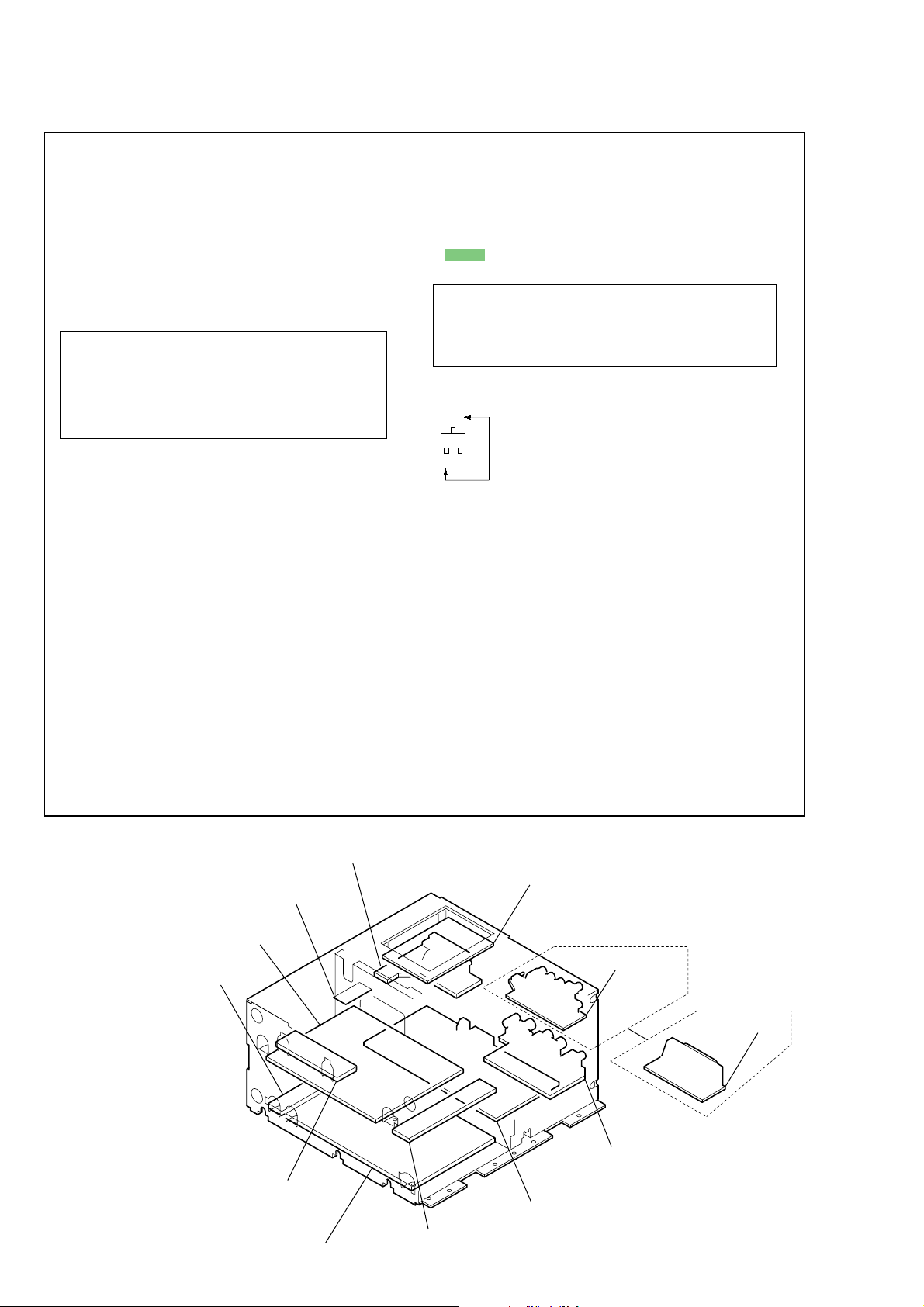
• Circuit Boards Location
PLF board
8
SPK-OUT board
BIND board
AMP board
15V-RELAY board
SWITCHING REGULATOR
DIA T TRANSMITTER board
EXCEPT AEP, UK, RU
COMPONENT board
AEP, UK, RU
SCART board
VIDEO-I/O board
SW-MAIN board
15V-REG board
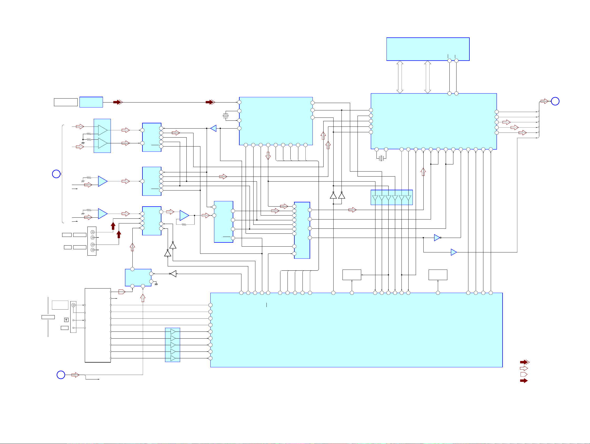
4-1. BLOCK DIAGRAM — AMP (DSP) SECTION —
IC527
S-RAM
SA-WSLF1
AUDIO (OUT)
SECTION
ANTENNA
VIDEO
SECTION
OPTICAL DIGITAL
IN
SW
B
VIDEO
SAT
FM 75 Ω
COAXIAL
AM
E
C
SL
SR R-CH
FL
FR R-CH
AUDIO IN
AUDIO IN
IC501
DIGITAL OPTICAL
IN
6
5
3
2
5
6
5
6
J501
L
R
L
R
TUNER PACK
GND
AM ANT
GND
TV-L
TV-R
IC507
AMP
-
+
+
-
IC508
AMP
+
-
IC509
AMP
+
-
R-CH
R-CH
L-CH
R-CH
MUTE
TUNED
STEREO
RDS IN
RDS DATA
7
1
7
7
CKFM ANT
CE
DI
DO
IC505
SELECTOR
R-CH
3
Y
0
Y
1
IC511
A/D CONVERTER
SCKI
1
LIN
DOUT
LRCK
2
RIN
PDWN
IC512
A/D CONVERTER
SCKI
DOUT
1
LIN
LRCK
PDWN
IC503
SELECTOR
12
X0
14
X1
15
X2
11
X3
10
A
1
9
B
Y
5
BCK
BCK
X
A
B
Q503
15
12
11
10
7
15
12
11
10
7
13
10
9
Q505
11
13
9
1
3
IC520
LEVEL SHIFT
Q504
10
12
8
2
4
A0 - A15
1 - 5
18 - 21
24 - 27
42 - 44
64 - 66
82 - 85
92 - 97
109, 110, 112
4
X500
24.576MHz
IC514
BUFFER
42
IC513
IC510
AMP
5
+
7
-
6
A/D CONVERTER
15
SCKI
1
LIN
55
TUN CLK
53
TUN CE
54
TUN DO
57
TU MUTE
51
TUNED
56
TU STEREO
52
TUN DI
94
RDS CLK
88
RDS DATA
DOUT
BCK
LRCK
PDWN
DIN1(I)
21
XOUT (O)
22
XIN(I)
20
XMCK(0)
CKOUT(O)15LRCK(O)14BCK(O)16DATA(O)35DO(O)
13
12
11
10
7
49
AVSEL248AVSEL147AVSEL0
DEMODULATOR
99
3
ADC PDOWN
IC519
DO
DIR/ADC 2
36
HDINCEHCLK
DO
25
DIR DO
DI(I)37CE(I)38CL(I)48XMODE(I)
2
3
5
6
11
10
14
13
1
CE
HDIN
7
20
DIG DI
XSTATE(O)
AUDIO (O)
ERROR(O)
IC522
SELECTOR
1A
1B
2A
2B
3A
3B
4A
4B
YB
HCLK
8
DIR CE
DIG CLK
XMODE
1Y
2Y
3Y
4Y
17
24
34
4
7
9
12
XMODE
24
DIR XMODE
Q514 Q515
23
DIR ANADIG
IC526 (1/3)
SYSTEM CONTROLLER
Q516
SWITCH
28
IC524
LEVEL SHIFT
DAMP MUTE
A0 - A15
69
G8
68
G9
30
SDI2
114
SDI3
59
EXLOCK
MCLK12MCLK235HDOUT31HACN32HDIN18SDI129BCKI217BCKI128LRCKI215LRCKI122KFSIO
9
X501
13.90MHz
119135
13
4
6
18
DIR ZERO
22
DIR XSTA
19
DIR ERR
17
DSP GP9
1082
6
DSP DO
12
15
DSP HACN
7 - 10
72 - 75
13 - 15
77 - 80
29 - 31
35 - 38
102 - 105
107, 108
D0 - D15
D0 - D15
AUDIO DSP
IC525
24
IC530
INVERTER
Q507
SWITCH
46
AU MUTE
CS
17WE6
44
45
CSO
WEO
24
IC521
LEVEL SHIFT
PM34HCS2XRST56BST
113
13
12
DSP BS14DSP CS
DSP REST
LRCKO
BCKO
SDO1
SDO2
SDO3
16
19
20
23
24
25
DSP BST
AUDIO (OUT)
D
SECTION
LRCKO
BCKO
D1
D2
D3
SCK
• R-ch is omitted due to same as L-ch.
• Signal Path
: DIGITAL IN
: AUDIO
: TUNER
: AUX IN (AUDIO)
SA-WSLF1
99
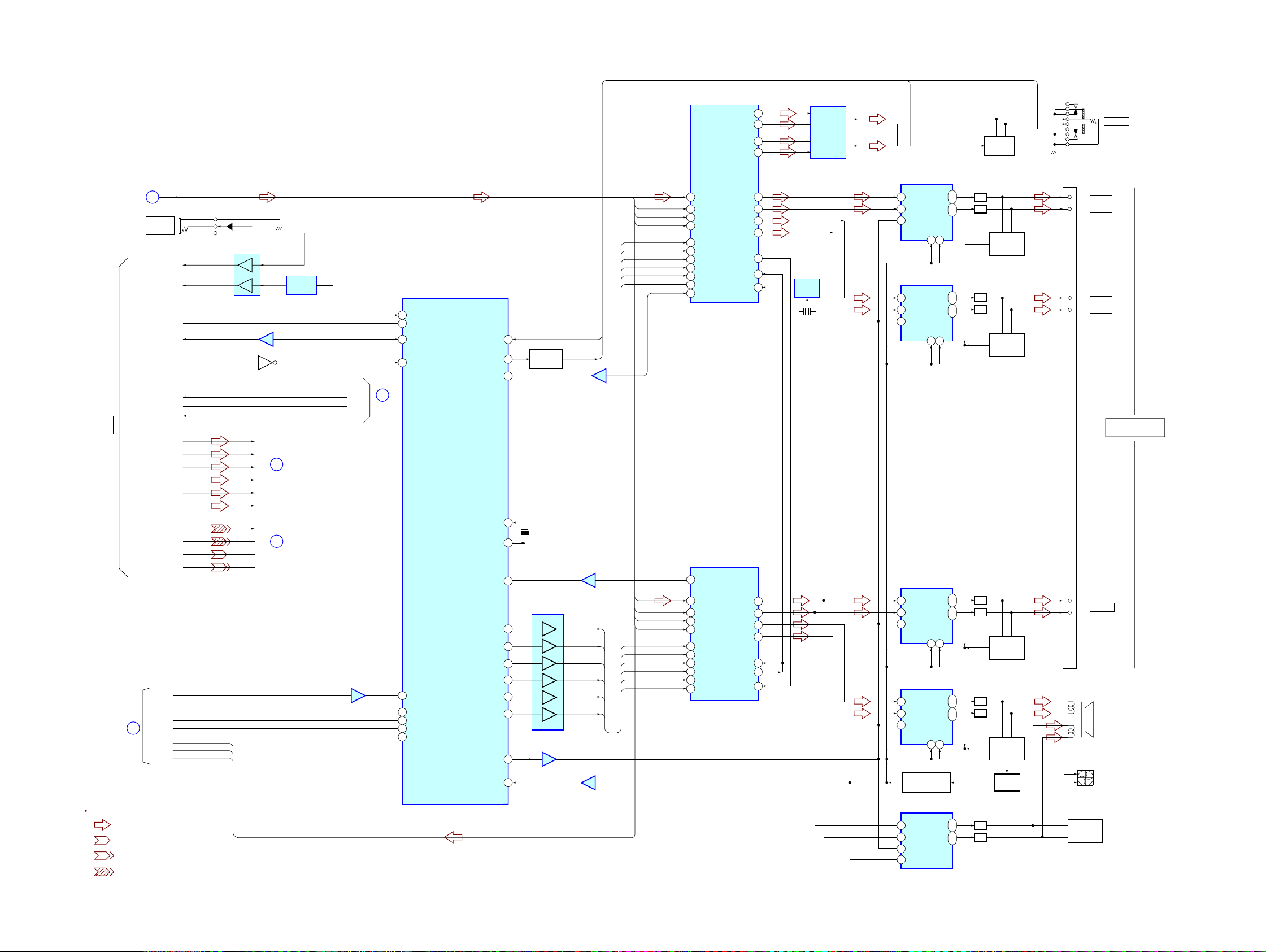
SA-WSLF1
— AUDIO (OUT) SECTION —
(TO CENTER SPEAKER SS-CTLF1)
SYSTEM
CONNECTOR
(TO MAIN UNIT HCD-LF1)
DIAT TRANSMIT
SECTION
Signal Path
AUDIO(DSP)
D
SECTION
REMOTE
CONTROL
AC DETECT/CABLE DET
AMPMICON RESET
CABLE-DET2
(AMP MICOM)
EVER 5.6V
PCONT1
CSOD
XRST
XLAT
SDATA
F
SCLK
D2(SL/SR)
BCKO
LRCKO
: AUDIO
: Y
: CHROMA
: COMPONENT VIDEO
D1 - D3, SCK,
BCKO, LRCKO
J502
SIRCS
DI
DO
+15V
C
SW
SL
SR
FL
FR
Cb/B
Cr/R
Y/CY/G
C/CVBS
BCKO
LRCKO
D2
IC506(1/2)
BUFFER
2
5
+6V
6
3
Q508
AUDIO(DSP)
17
IC506(2/2)
B
SECTION
C
VIDEO
SECTION
DETECTOR
BUFFER
IC531
AC-DEC
E5.6V
PCONT
+15V
IC523(1/4)
LEVEL SHIFT
31, 2
A
VIDEO
SECTION
34
RESET
100
IF-IN
1
DAMP DATA
90
STOP IN
95
DIAT CSOD
97
DIAT XRST
96
DIAT CS XLAT
4
DIAT DO
5
DIAT CLK
IC526 (2/3)
SYSTEM CONTROLLER
OVERFLOW1
OVERFLOW2
DAMP DATA
DAMP INIT
DAMP SOFTMUTE
DRIVE-RST
(D2)
HPSW
HP-MUTE
DAMP CLK
DAMP CS1
DAMP CS3
DRI-OCP
IC108
STREAM PROCESSOR
45
HPOUTL1
43
HPOUTL2
41
HPOUTR1
39
HPOUTR2
D1
SCK
BCKO
LRCKO
SCDT
SHIFT
LATCH1
INIT
NSPMUTE
SOFTMUTE
128
HP-SW
HP-MUTE
6
IC523(3/4)
LEVEL SHIFT
15
14
13
18
SOFTMUTE
17
11
IC523(4/4)
LEVEL SHIFT
IC523(2/4)
LEVEL SHIFT
4, 5
SCDT16
SHIFT
LATCH1
LATCH3
INIT
12, 13
9,108
D3
SCK
BCKO
LRCKO
SCDT
SHIFT
LAT3
INIT
NSPMUTE
SOFTMUTE
65
60
85
38
X2
X1
39
86
98
99
29
31
26
28
43
44
Q517
SWITCH
X502
20MHz
IC529(1/2)
LEVEL SHIFT
4
5
6
7
2
3
IC529(2/2)
LEVEL SHIFT
31
DATA
36
XFSIIN
30
BCK
29
LRCK
21
SCDT
22
SCSHIFT
23
SCLATCH
27
INIT
18
NSPMUTE
19
SOFTMUTE
24
OVF FLAGR
IC110
STREAM PROCESSOR
24
OVF FLAGR
31
DATA
36
XFSIIN
30
BCK
29
LRCK
21
SCDT
22
SCSHIFT
23
SCLATCH
27
INIT
18
NSPMUTE
19
SOFTMUTE
OUTL1
OUTL2
OUTR1
OUTR2
XFS0OUT
FSOI
XFSOIN
OUTL1
OUTL2
OUTR1
OUTR2
FSOI
FSOCKO
XFSOIN
11
9
6
4
14
38
48
11
9
6
4
38
37
48
IC305
OSC
X450
49.152MHz
IC301
HEADPHONE
AMP
HP-MUTE
IC101
POWER DRIVER
2
PWMBP
17
PWMAP
4
RESET
IC102
POWER DRIVER
2
PWMBP
17
PWMAP
4
RESET
IC105
POWER DRIVER
2
PWMBP
17
PWMAP
4
RESET
IC106
POWER DRIVER
2
PWMBP
17
PWMAP
4
RESET
Q301
PROTECT DETECT
IC107
POWER DRIVER
2
PWMBP
17
PWMAP
4
RESET
13
SD
OUTB
OUTA
8 13
OUTB
OUTA
8
OUTB
OUTA
8
OUTB
OUTA
8
OUTB
OUTA
DIAGA
DIAGA
13
DIAGA
13
DIAGA
13
Q903-905
MUTING
29
LPF
30
25
LPF
26
SD
29
30
25
26
SD
29
30
25
26
SD
29
30
25
26
SD
29
30
25
26
LPF
LPF
LPF
LPF
LPF
LPF
LPF
LPF
Q101, 102
OVER LOAD
DETECT
Q103, 104
OVER LOAD
DETECT
Q109, 110
OVER LOAD
DETECT
Q111, 112
OVER LOAD
DETECT
DRIVE
Q303,304
FAN
HP-SW
+12V
J906
Q113, 114
OVER LOAD
(+)
(–)
(+)
(–)
(+)
(–)
FAN
DETECT
J903
PHONES
FRONT
L
FRONT
R
(IMPEDANCE USE 4Ω)
CENTER
SUB WOOFER
SPEAKER
SPEAKER
SA-WSLF1
1010
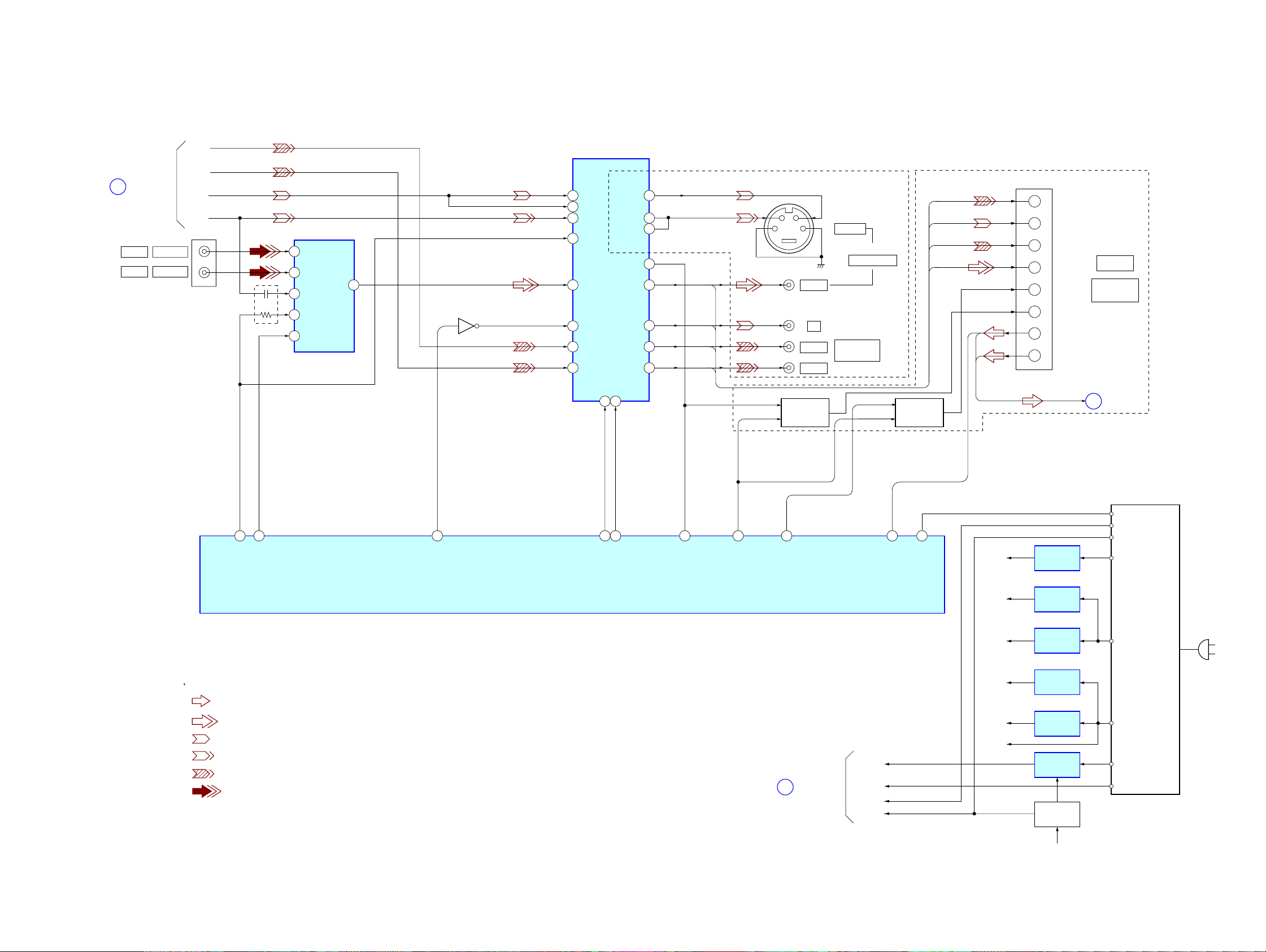
— VIDEO SECTION —
SA-WSLF1
C
VIDEO
SAT
AUDIO(OUT)
SECTION
VIDEO IN
VIDEO IN
Cb/B
Cr/R
Y/CY/G
C/CVBS
J904
AEP, UK, RU
1
3
5
4
2
IC903
SELECTOR
IN1
IN2
IN3
SW2
SW1
OUT
6
2
5
4
9
YIN
CYIN
CIN
YC-MIX
VIN
I/P
CBIN
CRIN
IC902
S-DCOUT
MUTE1
3
13
YOUT
COUT
CYBS
CYOUT
CBOUT
CROUT
MUTE2
AEP, UK, RUEXCEPT AEP, UK, RU
J905
21
26
27
25
S1
23
20
18
16
VOUT
CYOUT
CBOUT
CROUT
DVD SEL DVD SEL
34
12
VIDEO
PB/C
PR/C
Q907-909
FUNCTION
SWITCH
Y
B
R
S VIDEO
J907
MONITOR OUT
J909
COMPONENT
VIDEO OUT
RGB SEL
BLANKOUT
Q910-912
SWITCH
CROUT
CYOUT
CBOUT
VOUT
15
R/C OUT
G OUT
11
B OUT
7
CVBS OUT
19
BLANK
16
OUT
8
FUNCTION
L
R
SW
6
A(L) IN
2
A(R) IN
L, R
EURO AV
OUTPUT
(TO TV)T
AUDIO(DSP)
E
SECTION
VIDEO AMP, 75ohm DRIVER
10
7
Q913
12
14
Signal Path
69 72 63 50 61 62 70 73 7 11
YC-MIX
AVSEL5
IP SEL
IC526(3/3)
SYSTEM CONTROLLER
ALSEL4
AVSEL3
VS/WIDE
DVD SEL
RGB SEL
: AUDIO
: VIDEO
: Y
: CHROMA
: COMPONENT VIDEO
: AUX IN(VIDEO)
A
AUDIO(OUT)
SECTION
+15V
E5.6V
AC-DEC
PCONT1
IP-SW
P-PWM
+2.5V
+5V
+5V
+9V
+9V
+12V
+15V
IC528
+2.5V REG
IC516
+5V REG
IC515
+5V REG
IC517
+9V REG
IC518
+9V REG
IC800
+9V REG
Q506, Q801
SWITCH
SWITCHING
REGULATOR
V-CONT
AC-DEC
ON/OFF
(STANDBY/POWER)
3.3V
AC IN
6.2V
12V
+15V
E5.6V
SA-WSLF1
E5.6V
1111
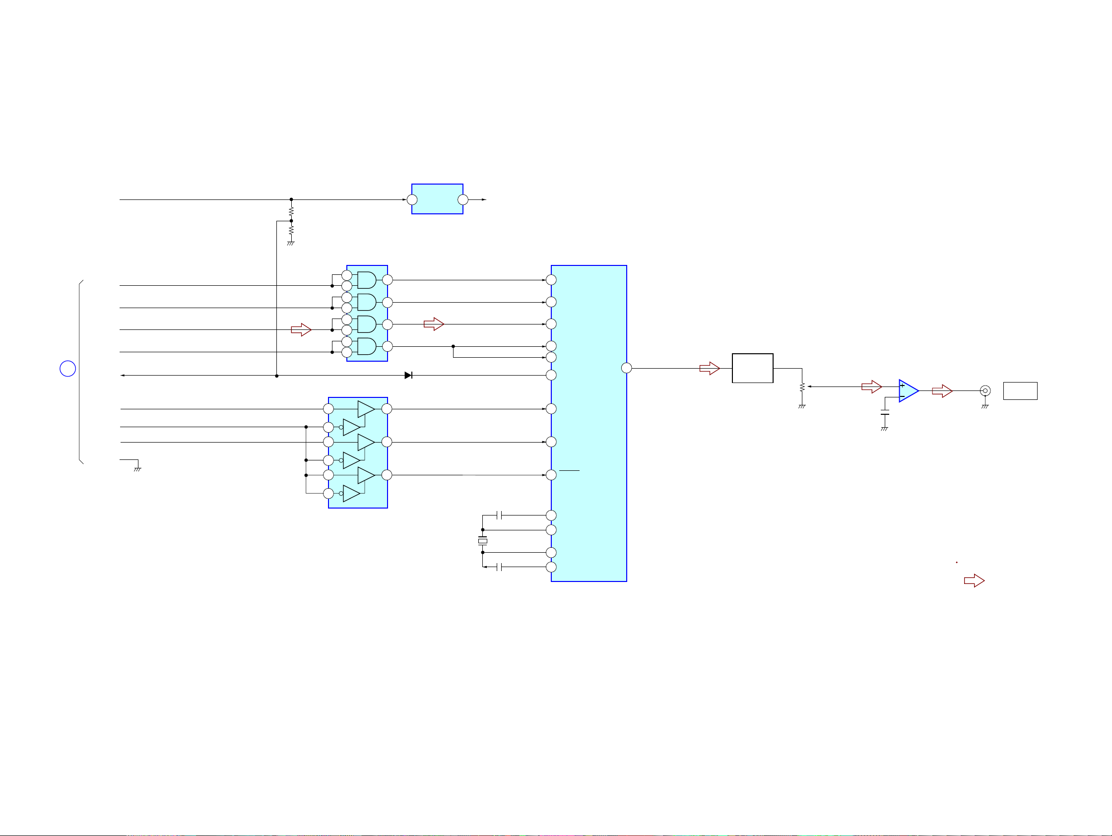
SA-WSLF1
— DIAT TRANSMITTER SECTION —
AUDIO(OUT)
SECTION
F
+9V
LRCKO
BCKO
D2(SL/SR)
XRST
CSOD
SDATA
XLAT
SCLK
D-GND
VCC(9V)
R835
R836
5
4
12
13
10
IC802
LEVEL SHIFT
4
5
10
9
13
12
1
2
6
8
11
3
D800
6
11
8
IC801
6 4
+2.5V REG
+2.5V
RF MODULATOR
D/A CONVERTER
49
LRCK
50
BCK
48
DTIN
41
APS
64
XRST
16
CSOD
15
SWDT
13
SCLK
14
XSCEN
IC804
DAAOUT
21
Q801
BUFFER
RV801
IC805
RF AMP
3
4
C842
1
J908
DIR-T1
TO
TRANSMITTER
(
DIR-T1
(
9
LEVEL SHIFT
IC803
X801
24.576MHz
C820
C819
54
57
59
60
C SST
O SCI
OSCO
XTCK4
Signal Path
: AUDIO
SA-WSLF1
1212
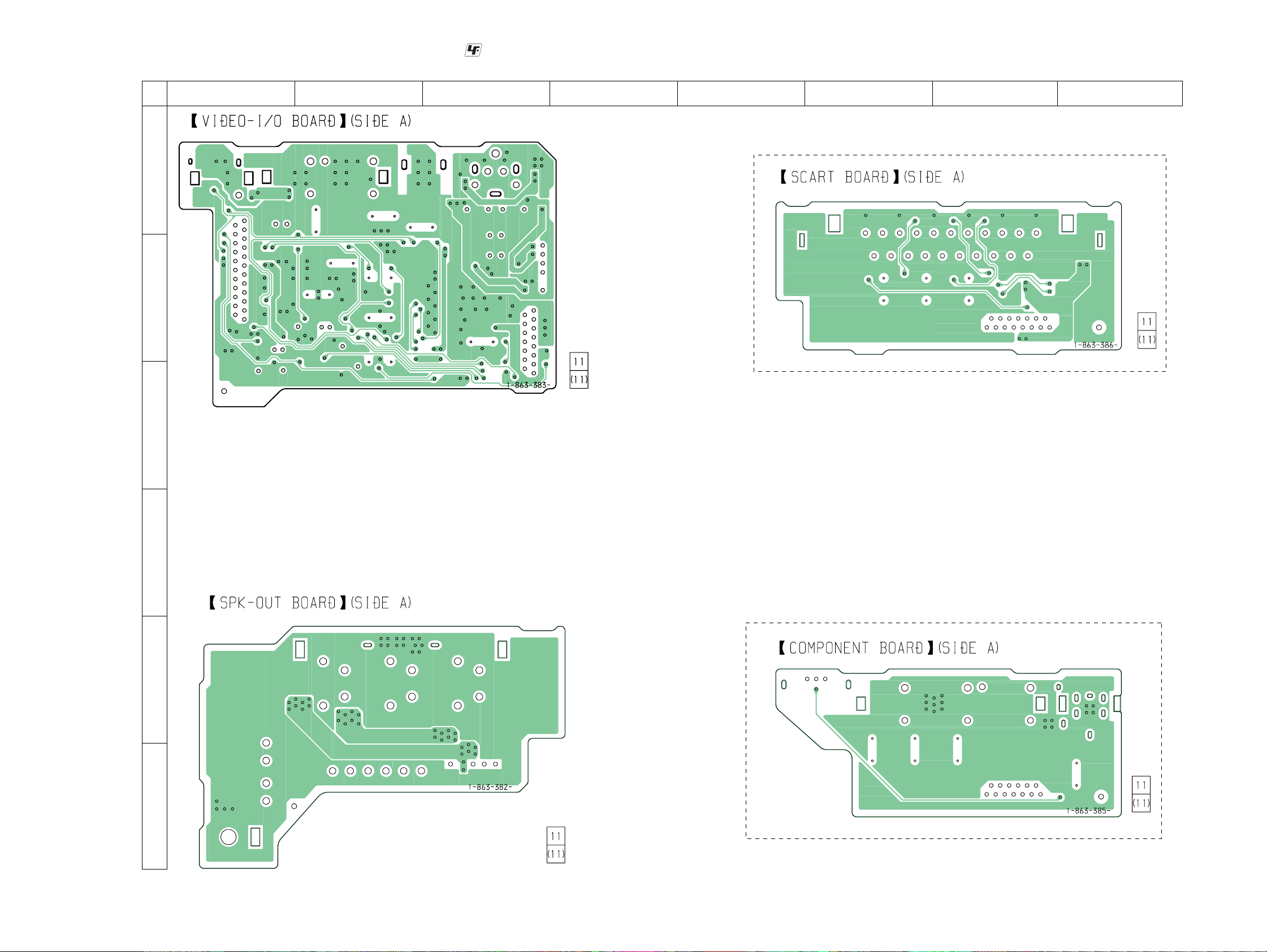
SA-WSLF1
4-2. PRINTED WIRING BOARD — JACK COMB SECTION (SIDE A) —
12
A
B
:Uses unleaded solder.
• See page 8 for Circuit Boards Location.
34567
AEP,UK,RU
8
C
D
E
EXCEPT AEP,UK,RU
SA-WSLF1
F
1313
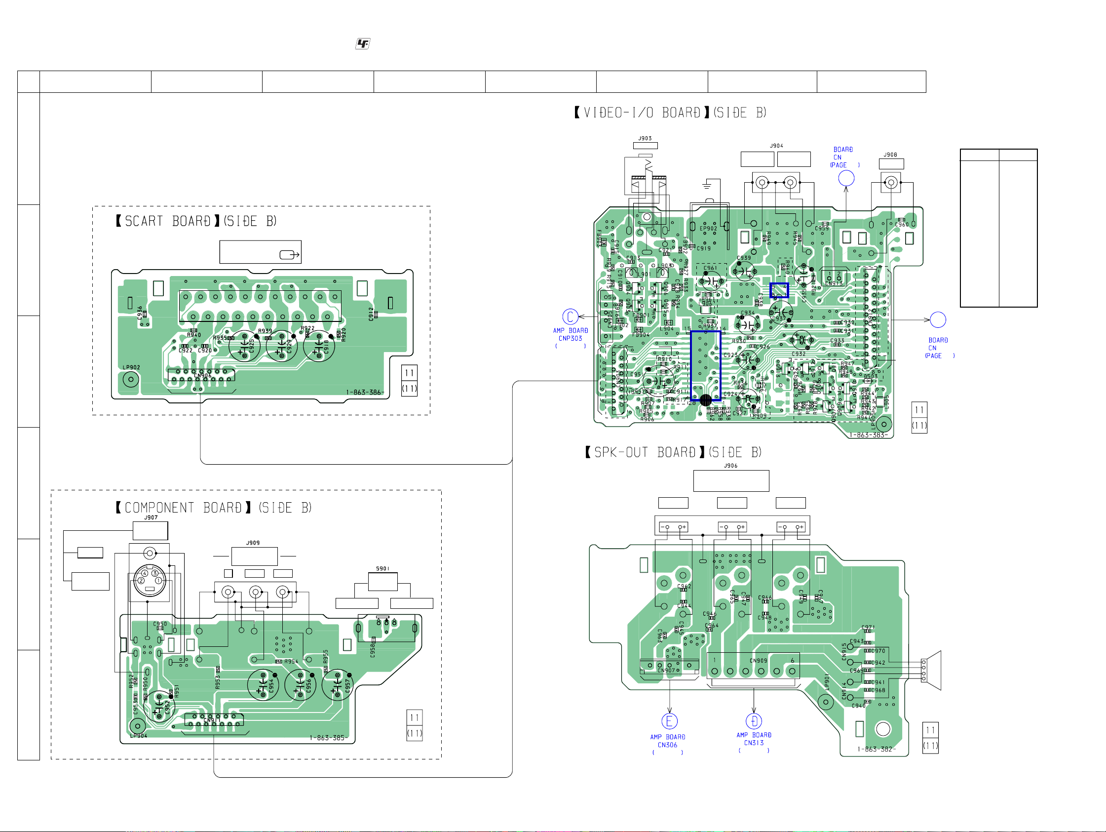
SA-WSLF1
4-3. PRINTED WIRING BOARD — JACK COMB SECTION (SIDE B) —
12
34567
A
AEP,UK,RU
J905
EURO AV
B
C
1
2
214
215
OUT PUT (TO TV)
20
:Uses unleaded solder.
• See page 8 for Circuit Boards Location.
8
• Semiconductor
Location
Ref. No.
D503 C-8
IC902 C-6
IC903 B-7
Q903 B-6
Q904 B-6
Q905 B-6
Q906 B-6
Q907 C-8
Q908 C-8
Q909 C-8
Q910 C-8
Q911 C-8
Q912 C-7
Q913 C-7
16
Location
SAT
DIAT TRANSMITTER
803
28
DIR-T1
PHONES
VIDEO
VIDEO IN
VIDEO IN
B
(CHASSIS)
EXCEPT
AEP,UK,RU
AEP,UK,RU
IC903
21
EXCEPT
AEP,UK,RU
Page 23
EXCEPT
AEP,UK,RU
1
2
EXCEPT
AEP,UK,RU
1
2
A
SW-MAIN
21
23
AEP,UK,RU
22
514
IC902
EXCEPT
13
15
14
AEP,UK,RU
AEP,UK,RU
AEP,UK,RU
D
E
F
EXCEPT AEP,UK,RU
VIDEO
S VIDEO
(DVD ONLY)
MONITOR
OUT
COMPONENT
VIDEO OUT
Y
PB/C
B
2
113
12
PR/C
SPEAKER
(IMPEDANCE USE 4Ω)
FRONT R CENTER
R
SELECTABLE INTERLACE
SCAN
SELECT
Page 23
Page 23
FRONT L
SUB
WOOFER
SA-WSLF1
1414
SA-WSLF1
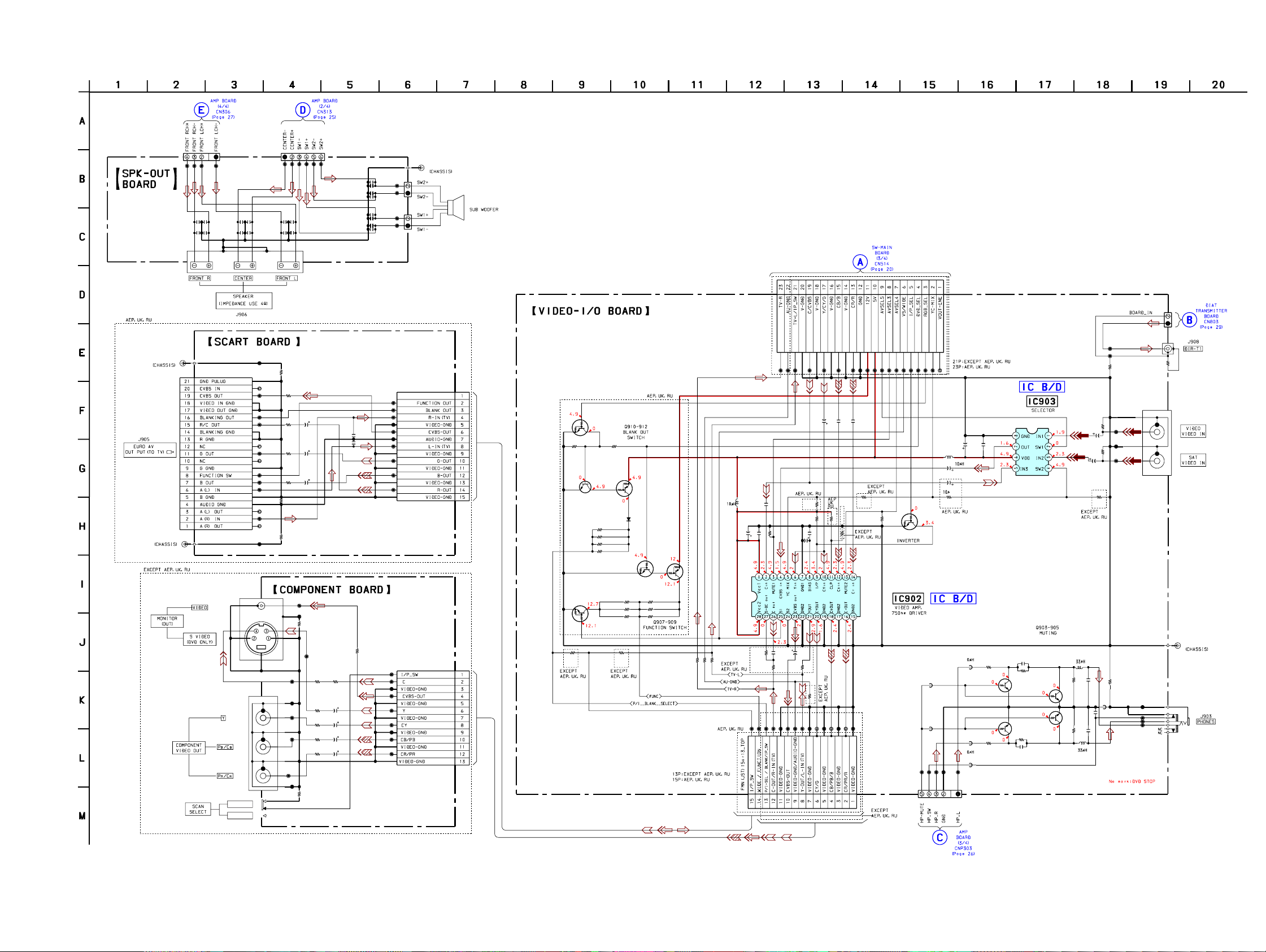
4-4. SCHEMATIC DIAGRAM — JACK COMB SECTION —
C962 C964
0.01 0.01
0.001
50V
E401
E402
J907
J909
TP995
TP994
B
TP997
TP996
C963 C965
0.01 0.01
0.001
50V
B
J905
21P
S901
CN907
4P
0.001
50V
B
SELECTABLE
INTERLACE
CN909
6P
TP988
C966
0.01
C948C945C944 C947C946
0.001
0.001
50V
50V
B
B
TP916
C912
TP917
TP918
1/10W
TP921
TP923
R922
1/10W
TP927
TP930
TP931
1/10W
TP934
TP937
R939
TP938
TP942
TP943
TP944
TP945
TP946
TP947
TP952
TP955
TP957
TP977
TP981
TP987
0
R920
75
75
R935
75
R940
C936
TP989
75 1/10W
0
TP992
TP991
TP990
C967
0.01
C949
0.001 50V B
C918
1000
6.3V
C925
1000
6.3V
C929
1000
6.3V
0
C950
0
TP948
R952
1/10W 0
R951
1/10W
R953
75 1/10W
R954
75 1/10W
R955
75 1/10W
C958
0
TP993
75
75
C940
C941
C942
C943
C953
C952
1000 6.3V
C954
1000 6.3V
C956
1000 6.3V
C957
1000 6.3V
C968
0.001 50V B
0.001 50V B
C969
C970
0.001 50V B
0.001 50V B
C971
C920
100p
50V
CH
R950
75
1/10W
0.01
0.01
0.01
0.01
C922
100p
50V
CH
• See page 32 for IC Block Diagrams.
CN914
2P
TP998
TP999
TP1000
TP1001
CN915
2P
TP919
TP920
TP922
TP924
TP925
TP926
TP928
TP932
TP935
TP939
TP949
TP950
TP951
TP953
TP954
TP958
TP960
TP978
TP982
EP901
15P
CN906
CN911
13P
Q912
DTC144EKA-T146
Q910
DTA114EKA-T146
R941
330 1/10W
330 1/10W
R942
330
R943
R944
330
1/10W
R928
R925
R923
R948
47k
1/10W
1SS355TE-1
R947
220k
1/10W
Q911
2SD601A-QR
S-TX
Q907
DTC144EKA-T146
R909 R956
D503
7
1/10W
Q909
DTC144EKA-T146
2.2k 1/10W
2.2k 1/10W
2.2k 1/10W
00
DTA114EKA-T146
R929
R926
R924
Q908
2.2k 1/10W
2.2k 1/10W
2.2k 1/10W
C932
*
1uF/50V: AEP, UK, RU
10uF/50V:EXCEPT AEP, UK, RU
0
0
0
6
907
R
R90
R905
CN903
*
CN913
2P
CN912
*
TP913
4
03
90
902
TP
TP9
TP
Q913
DTC144EKA- T146
6
P908
TP909
T
TP907
TP90
TP905
C938
C937
100
0.1
10V
25V
F
L906
C934
10 50V
C961
50V
R921
0
R934
L904
47
1/10W
FB904
0UH
FB901
0UH
56
959
TP979
TP976
TP9
TP
Q905 Q906
DTC343TK DTC343TK
Q903
DTC343TK
R916
L902
47
1/10W
FB903
0UH
980
TP
CN905
5P
IC903
NJM2235V
C928
0.0047
50V
B
47
1/10W
R915
Q904
47
1/10W
DTC343TK
C910
0.0047
50V
B
L903
R927R933
C921
4.7k
0.01
1/10W
25V
C913
R919
0.01
4.7k
25V
1/10W
L901
01
P891
T
TP892
C933
0.1
L905
25V
F
C927
0.1 25V F
C924
100
10V
W
/10
1
936
R
10k
C911R917
10k
0.1
1/10W
25V
3
964
TP965
TP
TP96
TP962
TP961
895
P893
T
TP894
TP
C931 C930
C932
*
10V
R962
0
10k
1/10W
F
6
C923
25V
22
C92
25V
0.1
C951
1000
6.3V
R911R957
00
0
R910
970
967
968
P969
P966
T
TP
TP972
TP971
TP
T
TP
99
P896
T
1
F
0
938
R
TP973
P900
TP8
TP898
TP9
TP897
T
1
10V
F
R961 R960
0 0
0
R930R958
10k
R937
1/10W
2
IC90
1623BFBE
M
M
975
TP
TP974
TP915
C959
0
R949
75
1/10W
TP929
C939
TP933
10 50V
R945
75
1/10W
TP936
C935
10 50V
C919
B
B
0
C915
0
0.1
B902
25V
F
F
WIRE
J908
1P
C960
0
J904
EP902
TP986
TP983
TP984
TP985
J903
HP JACK
SA-WSLF1
1515
SA-WSLF1
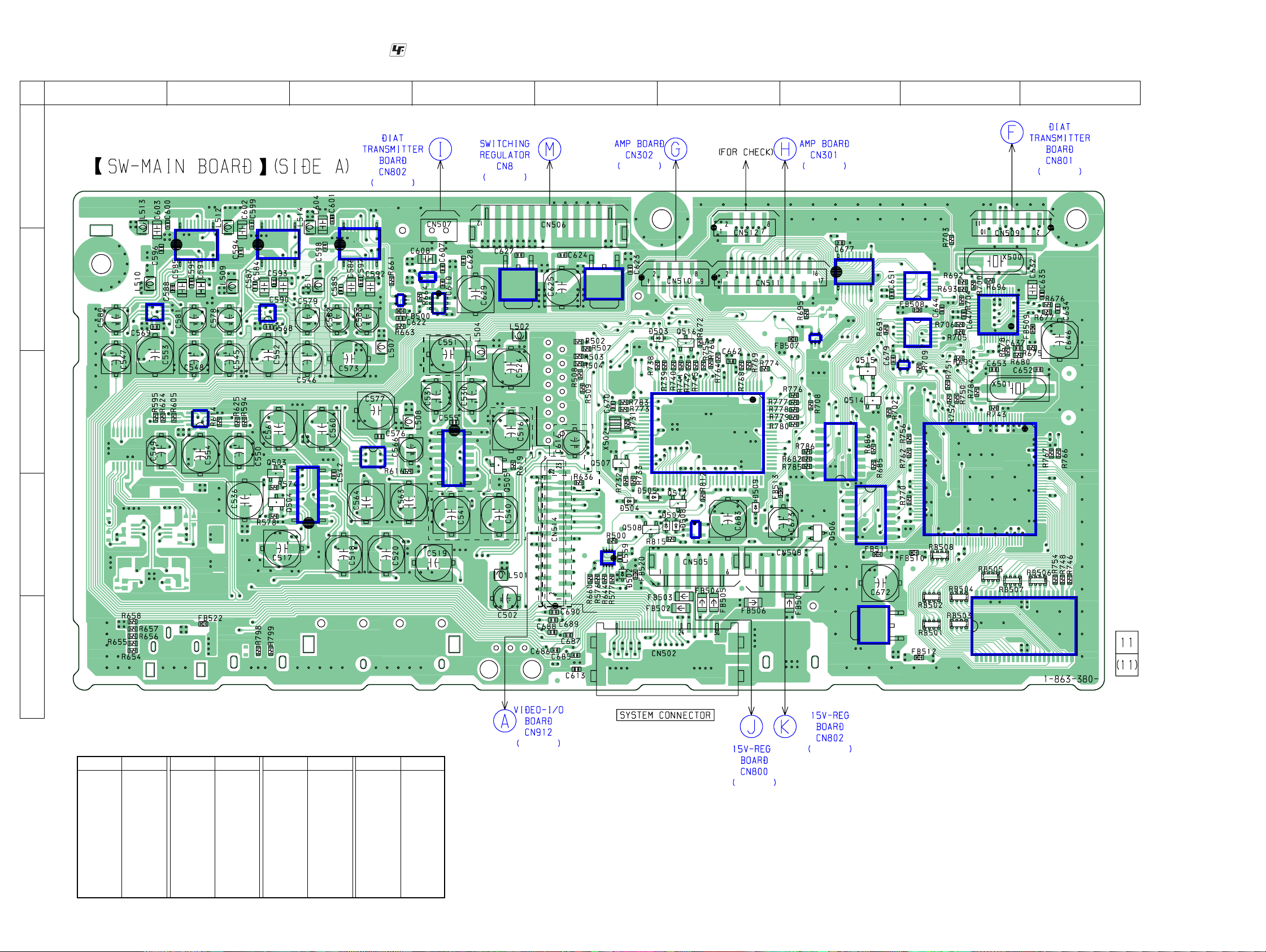
4-5. PRINTED WIRING BOARD — SW-MAIN SECTION (SIDE A) —
12
34567
A
IC512
20
1
IC511
20
11
10
11
1
10
IC513
20
1
B
C
IC508
5
8
4
1
4
5
8
1
IC509
4
5
8
1
IC507
9
E
E
16
8
IC503
1
1
45
IC510
D
Page 28
11
10
8
:Uses unleaded solder.
21
IC515
554
3
1
4
3
1
6
1
3
4
IC514
IC516
AEP,UK,RU
116
IC505
89
Page 30
3
IC518
AEP,UK,RU
• See page 8 for Circuit Boards Location.
Page 23
1
2
13
2
IC517
30
AEP,UK,RU
EXCEPT
AEP,UK,RU
21
4
IC506
58
31
E
50
51
E
E
1
E
IC526
5
1
3
IC531
4
1
100
8 9
Page 23
1120
IC523
87
1
10
IC529
4
5
3
1
IC521
7
8
81
80
14
IC520
1
1
3
45
E
IC530
E
14
14
1
16
1
89
IC522
1
30
31
25
36
24
37
IC519
13
48
IC525
IC524
E
7
8
60
61
Page 28
12
1
1
120
91
90
E
SA-WSLF1
• Semiconductor Location
Ref. No.
D502 D-5
D503 B-5
D504 D-5
D505 D-5
D507 D-6
D508 D-6
D509 D-6
IC503 D-3
IC505 C-4
IC506 D-5
IC507 B-2
Location
Ref. No.
IC508 B-1
IC509 C-2
IC510 C-3
IC511 A-2
IC512 A-2
IC513 A-3
IC514 B-3
IC515 B-4
IC516 B-4
IC517 B-5
IC518 B-4
IC519 C-8
Location
Ref. No.
IC520 C-7
IC521 B-7
IC522 B-7
IC523 B-8
IC524 D-7
IC525 D-8
IC526 C-6
IC527 E-8
IC528 E-7
IC529 B-7
IC530 C-8
IC531 D-6
Location
Ref. No.
Q503 C-2
Q504 D-3
Q505 D-4
Q506 D-7
Q507 C-5
Q508 D-5
Q514 C-7
Q515 C-7
Q516 B-6
Q517 D-6
Location
Page 14
EXCEPT
AEP,UK,RU
44 23
IC527
122
2
IC528
3
1
Page 30
Page 30
1616
SA-WSLF1
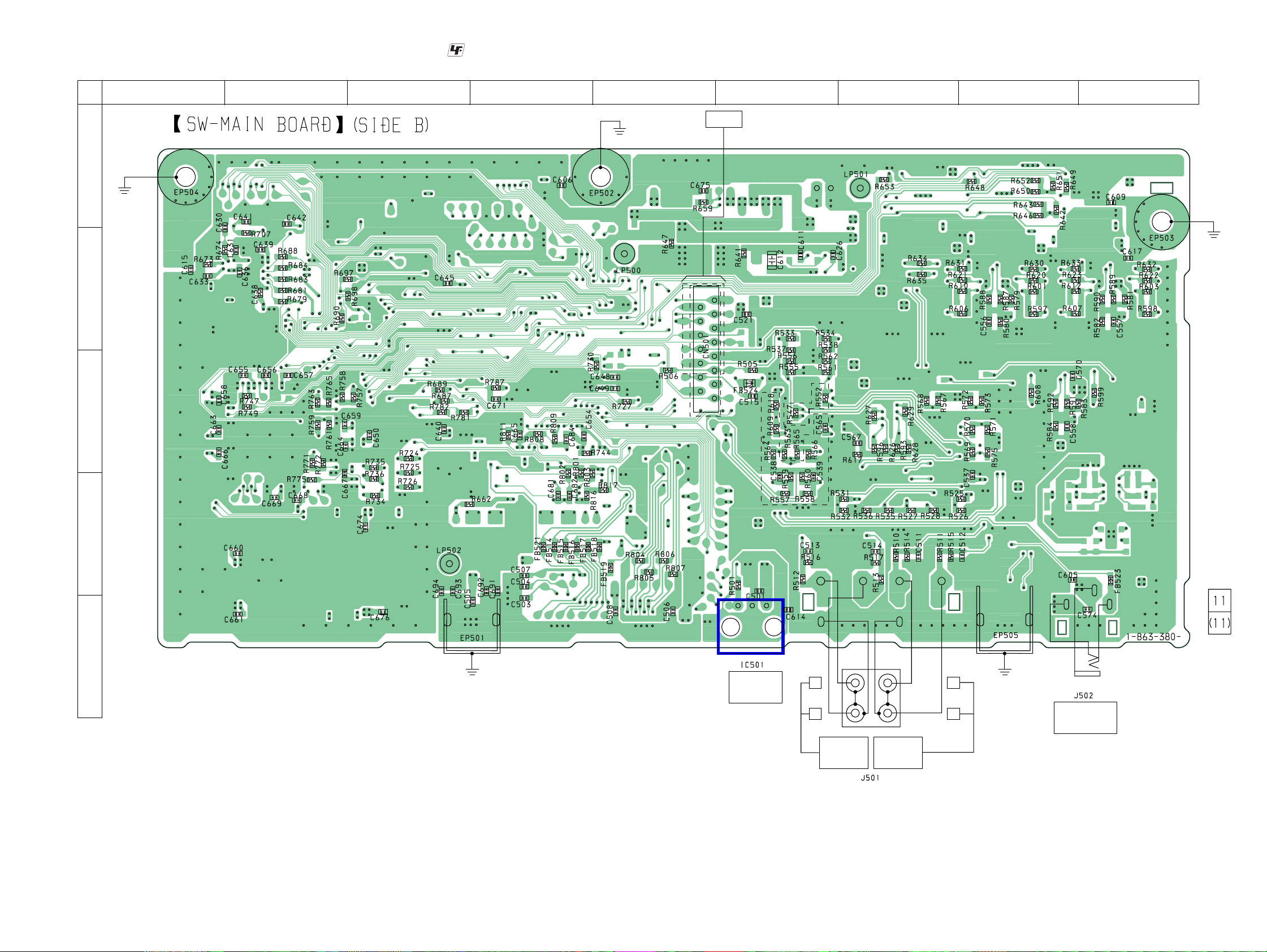
4-6. PRINTED WIRING BOARD — SW-MAIN SECTION (SIDE B) —
12
345678 9
A
(CHASSIS)
B
:Uses unleaded solder.
• See page 8 for Circuit Boards Location.
TUNER
(CHASSIS)
EXCEPT AEP,UK,RU
1
2
11
(CHASSIS)
C
D
E
14
AEP,UK,RU
15
AEP,UK,RU
13
EXCEPT
AEP,UK,RU
IC501
(CHASSIS) (CHASSIS)
OPTICAL
DIGITAL IN
L
R
L
R
REMOTE
CONTROL
SA-WSLF1
SAT
AUDIO IN
VIDEO
AUDIO IN
1717
SA-WSLF1
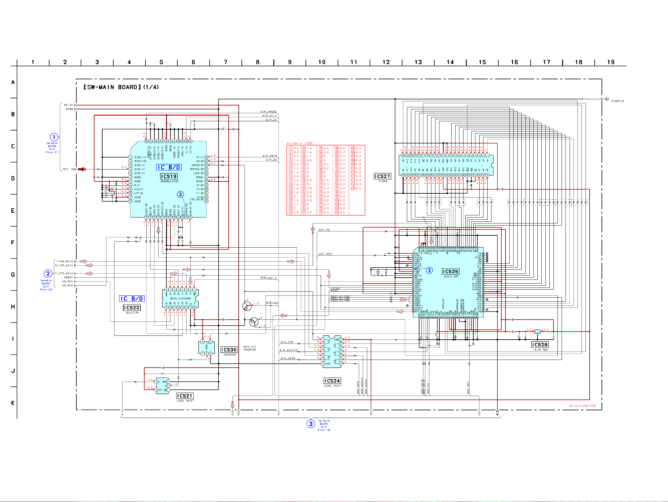
4-8. SCHEMATIC DIAGRAM — SW-MAIN SECTION (1/4) —
C637
R678
0.01
4.7k
16V
1/10W
B
R680
10k
1/10W
R675
100
1/10W
C633
R673
C634
R676
C635
C630
C631
C636
0.01
16V
B
0.01 16V B
33k 1/10W
0.1 25V F
4.7k 1/10W
0.01 16V B
0.1 25V F
0.1 25V F
1/10W
R677
5.6k
1/10W
IC519
LC89056W-E
R674
C632
100
10 10V
R692
R703
HS121
HS121
47
1/10W
R693
47
R704
1/10W
1/10W
1/10W
R679
R681
R683
1k
100
R695
68
1/10W
1/10W
100
R707
C641
1/10W
1/10W
C639
R684
R688
100
100
R690
100 1/10W
FB507
0UH
C645
0.1 25V F
• See page 33 for IC Block Diagrams. • See page 32 for Waveforms. • See page 36 for IC Pin Function Description.
C638
0.1
25V
F
1/10W
270
7p
X500
24.576MHz
0.1 25V F
R697
100
1/10W
R696
1M
C642
5p
R700
3.3k
0.1 25V F
C679
0.1 25V F
R698
100
C643
XX
R702
1k 1/10W
R699
R691
IC522
SN74LV157A
PWR
C644
IC530
MC74VHC1GU04DFT1
100 1/10W
100 1/10W
C646
FB509
220
0UH
4V
R705
100
1/10W
IC527
IS61LV6416
R706
3.3k
C647
0.1
25V
F
C653
12p
50V
Q514
DTC124EKA-
T146
Q515
DTC124EKA-
FB508
0UH
R709
22
1/10W
T146
R724
100
1/10W
1/10W
R725
100
1/10W
R726
100
IC524
TC74HCT700
7AF(EL)
1/10W
R734
100
100 1/10W
R736
100 1/10W
R735
-10TLT
RB506
100
1/16W
1/10W
1/10W
1/10W
C663
0.1
100
100
100
25V
F
R746
R748
R754
R767
10k 1/10W
R766
4.7k
1/10W
R747
R749
10k
4.7k
1/10W
1/10W
C652
C655
12p
0.1 25V F
50V
CH
R743
1/10W
R784
X501
R750
R751
R752
13.90MHz
C657
0.1 25V F
100 1/10W
100 1/10W
100 1/10W
680
1/10W
C650
0.1 25V F
CH
C658
0.1
25V
F
C656
0.1
25V
F
TP587
1M
TP586
R756 R762
100
1/10W
R758
10k
1/10W
R757
4.7k
1/10W
1/10W
4.7k
R759
1/10W
1/10W
C661
0.01
16V
B
IC525
*
C659
0.1
25V
F
100
R765
10k
R761
10k
1/10W
4.7k
1/10W
C615
0
C660
0.01
16V
B
RB507
100
1/16W
C666
0.1
25V
F
C667
0.1
C664
R770
0.1
25V
1/10W
F
25V
R772
10k
10k
1/10W
R771R763
4.7k
1/10W
FB512
0UH
RB505
100
1/16W
TP588
TP589
TP590
TP591
TP592
C668
0.1 25V F
C669
TP593
TP594
F
0.1 25V F
FB511
0UH
FB510
0UH
1/16W
RB504
100
100 1/10W
C672
220
4V
1/16W
100
NJM2391DL1
-26(TE1)
1/16W
RB502
100
IC528
RB503
R775
C674
0.1
25V
F
1/16W
1/16W
RB501
RB508
100
100
C676
0.1
25V
F
EP504
SA-WSLF1
IC521
SN74LVC1G1
25DCKR
1818
 Loading...