

SA-PSD5/WPSD5/
SS-SPSD5
SERVICE MANUAL
Ver 1.1 2004.02
With SUPPLEMENT-1
• The SA-PSD5 system consists of one unit
of SA-WPSD5 and five units of SS-SPSD5.
This system incorporates Dolby
Surround and the DTS** Digital Surround System.
Manufactured under license from Dolby Laboratories.
*
“Dolby,” “Pro Logic,” and the double-D symbol are trademarks of
Dolby Laboratories.
Manufactured under license from Digital Theater Systems, Inc. US
**
Pat. No. 5,451,942 and other worldwide patents issued and pending.
“DTS” and “DTS Digital Surround” are trademarks of Digital
Theater Systems, Inc. © 1996 Digital Theater Systems, Inc. All
rights reserved.
*
Digital and Pro Logic
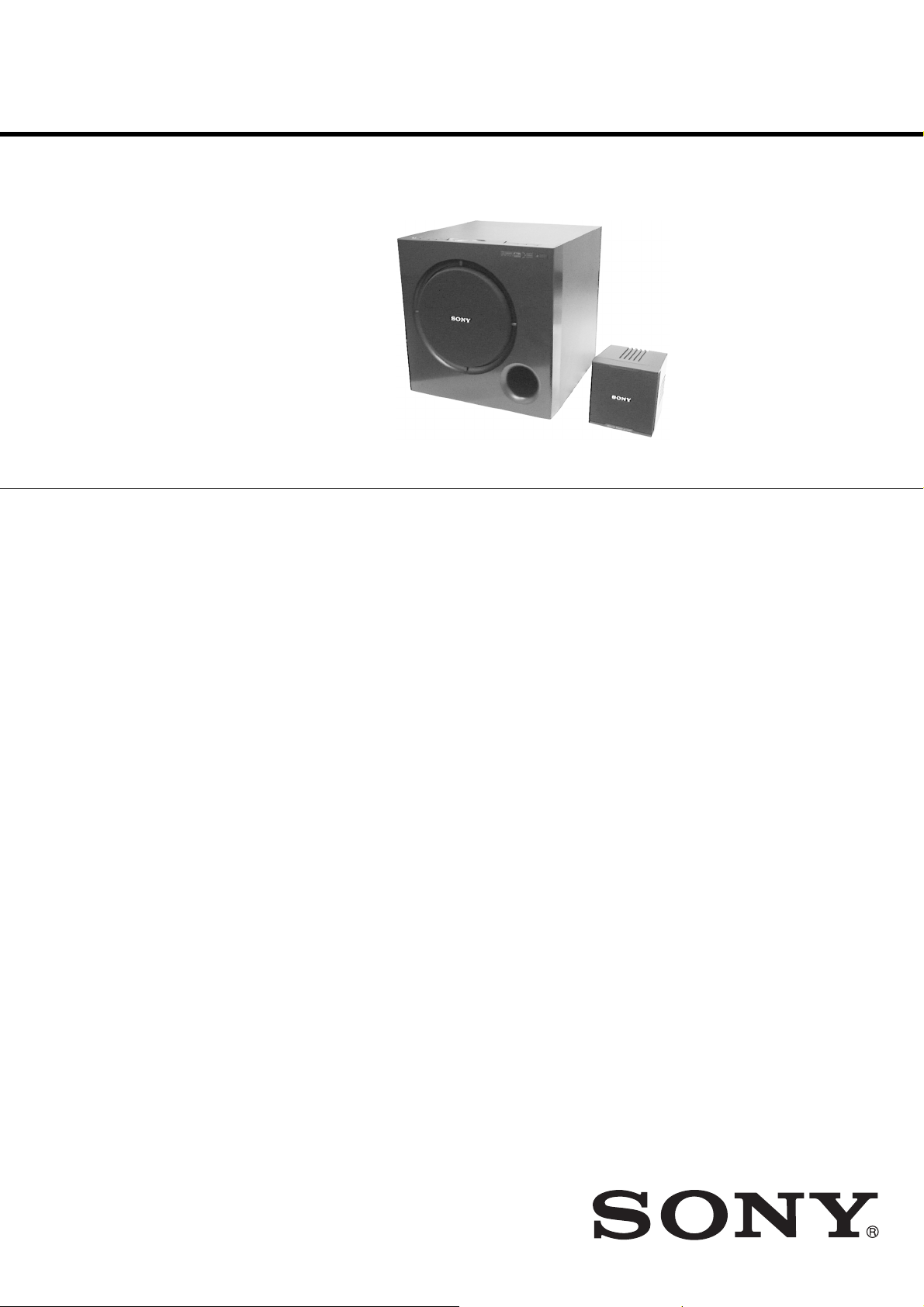
Photo: SA-WPSD5
US Model
Canadian Model
AEP Model
UK Model
E Model
Photo: SS-SPSD5
AUDIO POWER SPECIFICATIONS
POWER OUTPUT AND TOTAL HARMONIC DISTORTION:
SA-WPSD5 (subwoofer)
Max. output
Subwoofer: 80 W (4 ohms)
Front: 40 W + 40 W (6 ohms)
Center*: 40 W
Rear*: 40 W + 40 W
*Depending on the sound field settings and the source, there may be
no sound output.
With 3 ohm loads, both channels
driven, from 120 – 10,000 Hz; rated 25
watts per channel minimum RMS
power, with no more than 10 % total
harmonic distortion from 250
milliwatts to rated output.
SPECIFICATIONS
Speaker system Bass reflex
Speaker unit 200 mm (7
Rated impedance
Dimensions (approx.)
(11
Mass (approx.) 9.7 kg (21 lb 6 oz )
SS-SPSD5 (satellite speakers)
Speaker system Bass reflex
Speaker unit 77 mm (3
Rated impedance
Dimensions (approx.)
Mass (approx.) 780 g (1 lb 12 oz)
7
/8 inches) dia. cone type
4 ohms
300 × 300 × 300 mm
7
/8 × 11 7/8 × 11 7/8 inches) (w/h/d,
not including the projecting parts)
1
/8 inches ) dia. cone type
6 ohms
110 × 115 × 110 mm
3
(4
/8 × 4 5/8 × 4 3/8 inches) (w/h/d)
General
Power requirements
Power consumption
Operating temperature
Operating humidity
Supplied accessories
Design and specifications are subject to change without
notice.
120V AC, 60Hz (US, Canadian)
220 – 240 V
90 W (US, Canadian)
95 W (AEP, UK, E)
3.5 W (standby mode)
5˚C to 35˚C (41˚F to 95˚F)
5 % to 90 %
• Subwoofer (1)
• Satellite speakers (5)
• Speaker cords (5 m (17 ft) x 3, 15 m (50 ft) x 2)
• Optical digital cord (1)
• Remote commander (remote) RM-UP51 (1)
• R6 (size AA) batteries (2)
• Foot pads (20)
AC, 50/60 Hz (AEP, UK, E)
9-873-178-02
2004B16-1
© 2004.02
5.1ch DIGITAL AUDIO SYSTEM
Sony Corporation
Home Audio Company
Published by Sony Engineering Corporation
SA-PSD5/WPSD5/SS-SPSD5
TABLE OF CONTENTS
SAFETY CHECK-OUT ················································· 2
1. GENERAL········································································· 3
2. DIAGRAMS·······································································4
2-1. Circuit Boards Location ························································ 4
2-2. Block Diagrams ····································································5
2-3. Printed Wiring Board
– Digital Section (Side A) – ·················································· 6
2-4. Printed Wiring Board
– Digital Section (Side B) – ················································· 7
2-5. Schematic Diagram – Digital Section (1/2) – ······················· 8
2-6. Schematic Diagram – Digital Section (2/2) – ······················· 9
2-7. Schematic Diagram – LCD Section – ··································· 10
2-8. Printed Wiring Board – LCD Section – ································ 11
2-9. Schematic Diagram – Key Section – ···································· 12
2-10. Printed Wiring Board – Key Section –·································· 13
2-11. Schematic Diagram – IN/OUT Section – ·····························14
2-12. Printed Wiring Board – IN/OUT Section – ··························· 15
2-13. Schematic Diagram – Pre Amp Section –····························· 16
2-14. Printed Wiring Board – Pre Amp Section – ·························· 17
2-15. Schematic Diagram – Power Section (1/2) – ························ 18
2-16. Schematic Diagram – Power Section (2/2) – ························ 19
2-17. Printed Wiring Board – Power Section – ······························ 20
2-18. IC Block Diagrams ······························································· 21
2-19. IC Pin Function Description ·················································23
3. EXPRODED VIEWS·······················································25
3-1. SA-WPSD5 (FRONT SECTION)·········································25
3-2. SA-WPSD5 (AMP SECTION) ············································· 26
3-3. SS-SPSD5 ············································································· 27
SAFETY CHECK-OUT
After correcting the original service problem, perform the
following safety checks before releasing the set to the customer:
Check the antenna terminals, metal trim, “metallized” knobs, screws,
and all other exposed metal parts for A C leakage. Check leakage as
described below.
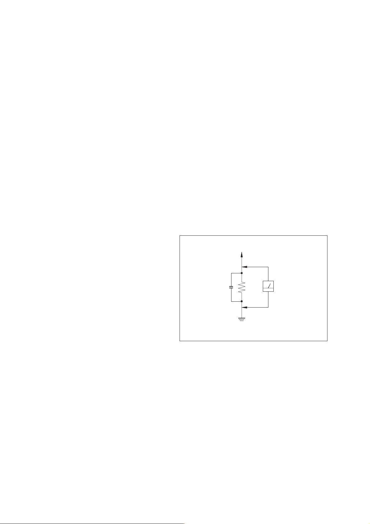
LEAKAGE
The AC leakage from any exposed metal part to earth ground
and from all exposed metal parts to any exposed metal part having
a return to chassis, must not exceed 0.5 mA (500 microamperes).
Leakage current can be measured by any one of three methods.
1. A commercial leakage tester, such as the Simpson 229 or RCA
WT -540A. Follo w the manufacturers’ instructions to use these
instruments.
2. A battery-operated AC milliammeter. The Data Precision 245
digital multimeter is suitable for this job.
3. Measuring the voltage drop across a resistor by means of a
VOM or battery-operated A C voltmeter . The “limit” indication
is 0.75 V, so analog meters must have an accurate low-voltage
scale. The Simpson 250 and Sanwa SH-63Trd are e xamples of
a passive VOM that is suitable. Nearly all battery operated
digital multimeters that have a 2V AC range are suitable. (See
Fig. A)
T o Exposed Metal
Parts on Set
4. ELECTRICAL PARTS LIST········································ 28
SAFETY-RELATED COMPONENT WARNING!!
COMPONENTS IDENTIFIED BY MARK 0 OR DOTTED LINE WITH
MARK 0 ON THE SCHEMATIC DIAGRAMS AND IN THE PARTS
LIST ARE CRITICAL TO SAFE OPERATION. REPLACE THESE
COMPONENTS WITH SONY PARTS WHOSE PART NUMBERS
APPEAR AS SHOWN IN THIS MANUAL OR IN SUPPLEMENTS
PUBLISHED BY SONY.
Flexible Circuit Board Repairing
• Keep the temperature of soldering iron around 270˚C
during repairing.
• Do not touch the soldering iron on the same conductor of the
circuit board (within 3 times).
• Be careful not to apply force on the conductor when soldering
or unsoldering.
AC
0.15 µF
Fig. A. Using an AC voltmeter to check AC leakage.
ATTENTION AU COMPOSANT AYANT RAPPORT
LES COMPOSANTS IDENTIFÉS P AR UNE MARQUE 0 SUR LES
DIAGRAMMES SCHÉMA TIQUES ET LA LISTE DES PIÈCES SONT
CRITIQUES POUR LA SÉCURITÉ DE FONCTIONNEMENT. NE
REMPLACER CES COMPOSANTS QUE PAR DES PIÈSES SONY
DONT LES NUMÉROS SONT DONNÉS DANS CE MANUEL OU
DANS LES SUPPÉMENTS PUBLIÉS PAR SONY.
1.5 kΩ
Earth Ground
À LA SÉCURITÉ!
Voltmeter
(0.75 V)
Notes on chip component replacement
• Never reuse a disconnected chip component.
• Notice that the minus side of a tantalum capacitor may be
damaged by heat.
2
SECTION 1
18
GB
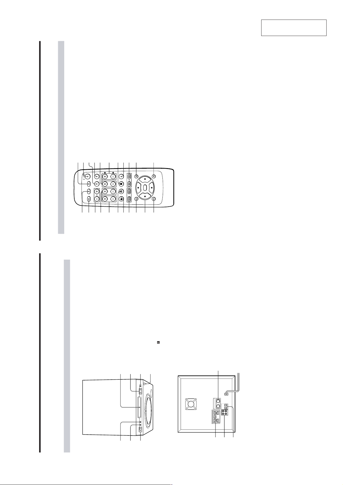
Index to Parts and Controls
Top panel/Front panel
1 SOUND FIELD button (11)
Selects the sound field.
2 FUNCTION button (9)
Selects the input signal.
3 ?/1 (POWER) switch and indicator (9)
Turns on and off the power of the system.
4 Display window (7, 9, 11, 14)
Indicates the speaker setting, input signal, sound field
mode, etc.
5 MASTER VOL (volume) +/– buttons (9)
Adjust the volume.
6 MUTING button (9)
Mutes the sound.
7
remote sensor (4)
Accepts the remote control signals.
Rear panel
8 SPEAKER jacks (5)
Connect to the supplied satellite speakers.
9 AUDIO IN 1/2 jacks (6)
Connect to the audio output of a TV, VCR, PSone, etc.
0 DIGITAL IN OPTICAL 1/2 jacks (5, 6)
Connect to the DIGITAL OUT (OPTICAL) jack of the
“PlayStation 2,” DVD player, etc.
qa BASS CONTROL knobs (10)
Make fine adjustment of the bass sound.
Refer to the pages indicated in parentheses for details.
Subwoofer
1
2
3
4
5
6
7
8
9
q;
qa
ONLY FOR
SS-SPSD5
FRONT R CENTER
SPEAKER
FRONT L
REAR R REAR L
2
OPTICAL
2
MID
LOW HIGH
MIN MAX
LEVEL FREQUENCY
1
1
L
R
BASS CONTROL
AUDIO IN
DIGITAL IN
19
GB
Remote
1 TV button (15)
Turns the TV on and off.
2 SHIFT button (7, 10, 14, 15)
Switches the function of the buttons on the remote.
3 TV CH +/– (TV/VIDEO) buttons (15)
Changes the TV channel.
To change the TV input, press – while pressing SHIFT.
4 REAR +/– buttons (10)
Adjust the rear speakers volume.
5 CENTER +/– buttons (10)
Adjust the center speaker volume.
6 XPAUSE button (13)
Pauses playing a disc.
7 NPLAY button (13)
Plays a disc.
8 ./>PREV/NEXT buttons (13)
Press to go to the next chapter or track, or to go back
to the previous chapter or track.
9 TITLE button (13)
Displays the title menu on the TV screen.
0 </M/m/,/ENTER button
Selects and executes the items or settings.
qa DISPLAY button (14)
Displays the setup display of the
“PlayStation 2” or
DVD player.
qs DVD 1/DVD 2 button (13)
Turns on and off the power of the DVD player.
qd ?/1 (POWER) switch (7, 9)
Turns on and off the system.
qf FUNCTION button (9)
Selects the input signal.
qg SOUND FIELD (SPEAKER SETUP) button (7, 11, 14)
Selects the sound field mode.
Pressing this button while pressing SHIFT will select
the speaker setup parameters.
qh WOOFER +/– buttons (10)
Adjust the subwoofer volume.
qj VOLUME +/– buttons (7, 9, 14)
Make the speaker settings or adjust the volume of the
system.
Pressing this button while pressing SHIFT will set the
speaker setup parameters.
qk xSTOP button (13)
Stops playing a disc.
ql MUTING (TEST TONE) button (9, 10)
Mutes the sound.
Pressing this button while pressing SHIFT will sound
the test tone.
w; m/M (SCAN) buttons (13)
Locate a point while monitoring the picture.
wa DVD MENU button (13)
Displays the DVD menu on the TV screen.
ws RETURN button (14)
Returns to the previously selected screen.
1
2
3
4
5
6
7
8
9
q;
qa
qs
qd
qf
qg
qh
qj
qk
ql
w;
wa
ws
SHIFT
TV CH
CENTER
FUNCTION
PLAY PAUSE
PREV NEXT SCAN
STOP MUTING
LEVEL
TV/
VIDEO
SPEAKER SET UP
FIELD
SOUND
TV DVD1
DVD2
REAR
WOOFER
TEST TONE
ENTER
DVD CONTROL
DVD MENU
TITLE
RETURNDISPLAY
VOLUME
GENERAL
SA-PSD5/WPSD5/SS-SPSD5
This section is extracted
from instruction manual.
3
SA-PSD5/WPSD5/SS-SPSD5
d
d
d
SECTION 2
DIAGRAMS
THIS NOTE IS COMMON FOR PRINTED WIRING BOARDS AND SCHEMATIC DIAGRAMS.
(In addition to this, the necessary note is printed in each block.)
Note on Schematic Diagram:
• All capacitors are in µF unless otherwise noted. p: pF.
50 WV or less are not indicated except for electrolytics
and tantalums.
• All resistors are in Ω and 1/
specified.
f
•
• C : panel designation.
• A : B+ Line.
• B : B– Line.
• Voltages and waveforms are dc with respect to ground
• Voltages are taken with a V OM (Input impedance 10 MΩ).
• Waveforms are taken with a oscilloscope.
• Circled numbers refer to waveforms.
• Signal path.
• Abbreviation
: internal component.
Note:
The components identified by mark 0 or dotted
line with mark 0 are critical for safety.
Replace only with part
number specified.
under no-signal (detuned) conditions.
Voltage variations may be noted due to normal produc-
tion tolerances.
Voltage variations may be noted due to normal produc-
tion tolerances.
F : AUDIO (ANALOG)
J : AUDIO (DIGITAL)
CND : Canadian model.
SP : Singapore model.
4
W or less unless otherwise
Note:
Les composants identifiés par
une marque 0 sont critiques
pour la sécurité.
Ne les remplacer que par une
piéce portant le numéro
spécifié.
Note on Printed Wiring Board:
• X : parts extracted from the component side.
• Y : parts extracted from the conductor side.
• x : parts mounted on the conductor side.
a
•
• : Pattern from the side which enables seeing.
(The other layers' patterns are not indicated.)
• Indication of transistor
Caution:
Pattern face side: Parts on the pattern f ace side seen from
(SIDE A) the pattern face are indicated.
Parts face side: Parts on the par ts face side seen from
(SIDE B) the parts face are indicated.
: Through hole.
C
Q
These are omitte
EB
C
EB
These are omitte
2-1. Circuit Boards Location
LCD board
KEY-R board
SIRCS board
PRE AMP board
DIGITAL board
KEY-L board
POWER board
ADJ boar
INPUT board
• WAVEFORMS
IC815 wz XOUT
1
81.4 ns
IC815 qg LRCK
3
20.8 µs
IC815 qd CKOUT
5
81.4 ns
6.5
Vp-p
4.7
Vp-p
5.6
Vp-p
IC815 w; XMCK
2
81.4 ns
IC815 qf BCK
4
325 ns
IC701 qd XOUT
6
62.5 ns
6.1
Vp-p
5.6
Vp-p
5.0
Vp-p
SP board
4
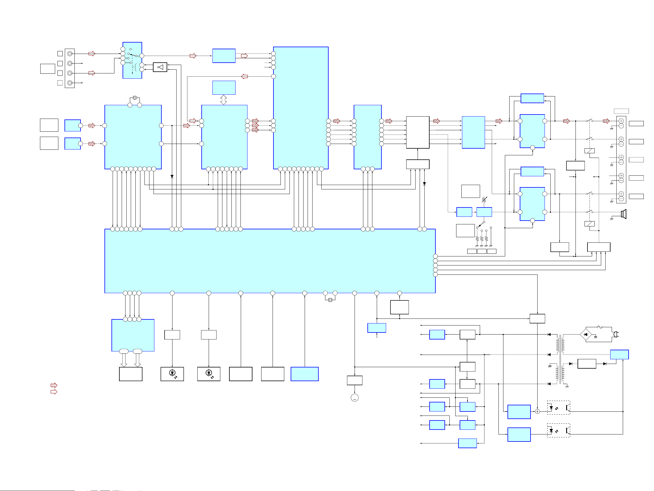
2-2. BLOCK DIAGRAMS
L
J601
AUDIO
IN
IC601
DIGITAL
OPTICAL
IN
IC602
DIGITAL
OPTICAL
IN
R
L
R
OUT
OUT
R-CH
R-CH
1
1
SELECT
IC812(1/2)
1
5
2
4
3 84
DIN0 SDIA0DATAO
DIGITAL AUDIO I/F
4
DIN1
34 14 13
87
86
85
DIRDI
DIRDO
DIRERR
(2/2)R-CH
X801
12.288MHz
21
XOUT
IC815
84
83
DIRCDE
B
A
XMODE
CLK38CE37DI36DO35ERROR
48
82
DIRCLK
MODEL1
22
17
75
3
9
10
XIN
XSTATE
15
RDS2
BCK
Q801,802
LRCK
INVERT
CKOUT
16
D801
19
88
20
ZERO
ASEL1
ASEL2
85
SDIA1
AC-3,PROLOGIC,
820
XIXMCK
PROGRAMMABLE DSP
SDWCK0
SDBCK0
82
83
BALANCE
AMP
IC813
256k bit
SRAM
IC802
DTS DECODER,
IC801
69
7
5
6
84
YSSSI
YSSSO
YSSSCK
83
DIRCLK
DIRCDE
/IC62/CSB65/CS66SO67SI68SCK
82
MODEL1
R-CH
47
30
29
32
31
9
745
646
8
SYSTEM CONTROL
IC701
LIN+
LINRIN+
RIN-
SDTO
SDTI2SDOB2
SDTI1SDOB1
SDTI3SDOB0
BCLK4LRCK5MCLKI
39
DAC
SURROUND
IC803
3
67PD68
69
SMUTE
70CS71
CDT1
CCLK42CDT143PD17S/M
CLK
CS41VREFL33XTI
38
SA-PSD5/WPSD5/SS-SPSD5
FEED BACK
IC302
R-CH
R-CH
J671
SPEAKER
FRONT L
REAR L
FRONT R
REAR R
CENTER
SP901
WOOFER
EVR
IC604
L
423
LINALOUT3
R
C
W
SL
SR
LOUTA
2524
RINAROUT3
ROUTA
725
LINBLOUT2
LOUTB
2226
RINBROUT2
ROUTB
10
LINCLOUT1
LOUTC
1928
RINCROUT1
ROUTC
CK14DATA15STB
16
58
57
56
VOL-CE
VOL-CLK
VOL-DAT
L
3
R
26
C
6
23
9
SR
20
MUTE
W
Q601-6
SL
MUTE SW
Q803-6
61
11
AN/DIG
LR-MUTE
AMP-MUTE
FAULT
SLEEP
F-RLY
300kHz
D704
L
R
C
W
SL
SR
63
54
45
43
2
PRE AMP
IC1001,1002,
IC1201,1202,
IC1401
RV601
BASS
CONTROL
FREQUENCY
AMP
IC606
S601
BASS
CONTROL
LEVEL
HIGH MID LOW
LPF
IC605
R-CH
R-CH
OFF
23
VINV1
POWER AMP
2627
VINV2
23
VINV1
POWER AMP
26
VINV2
OUT1
IC301
OUT2
MUTE
24
FEED BACK
IC202
OUT1
IC201
OUT2
MUTE
24
10
7
10
7
ERROR DET
Q201
ERROR DET
Q301
RY201
RY301
R-CHR-CH
RELAY DRIVE
Q391-5
• RCH is omitted
• Signal Path
: DIGITAL INPUT
: ANALOG INPUT
36
61
LCD DRIVE
S1-48
1-48
LCD401
FLINH
38
62
INH
IC401
LCD
FLCS
FLCLK
37
63
CE
CL
COM0-3
55-52
XOUT
FLDATA
35
64
DI
D1/P1
25
SWITCH
Q401-403
BACK LIGHT
D401-403
STBY
39
SWITCH
Q431-433
POWER
D431
KEY2
92
KEY INPUT
S431-434
KEY1
93
KEY INPUT
S451-453
SIRCS
42
REMOTE CONTROL
RECEIVER
IC471
XIN
X701
16MHz
1315
44
SWITCH
Q396
M
M901
FAN
MOTOR
POWERY
STOP
56
AC OFF DET
IC702
EVER+5.6V
RESET
12
POWER ON
RESET
Q701
+28V
+15V
+10V
-15V
-28V
A+9V
A+5V
D+5V
D+3.3V
EVER+5.6V
+15V REG
IC904
-15V REG
IC903
+5V REG
IC816
+3.3V REG
IC818
SWITCH
Q905
CONT
Q904,906
SWITCH
Q902
SWITCH
IC906
SWITCH
IC907
+5.6V REG
IC905,D909
OVER
CURRENT DET
IC902
OVER
CURRENT DET
IC910
SWITCH
Q912,913
D907
D906
D908
T901
ISOLATION
PC901
ISOLATION
PC902
D902
RECT
D901
REG
Q901,D911
F901
D904
AC IN
SWITCHING
IC901
55

SA-PSD5/WPSD5/SS-SPSD5
2-3. PRINTED WIRING BOARD – DIGITAL SECTION (SIDE A) –
• See page 4 for Circut Borads Lacation.
(Page 17) (Page 15) (Page 15)
IC 818
(Page 11)
• Semiconductor Location
Ref. No. Location
∗ D701 B-6
∗ D702 A-6
∗ D703 B-6
D704 B-1
∗ D705 A-6
∗ D706 A-6
∗ D707 B-6
∗ D801 B-5
∗ D802 C-3
∗ D803 C-3
D804 B-3
D805 B-3
∗ D881 B-1
∗ D882 B-1
∗: SIDE B
Ref. No. Location
∗ IC604 B-2
∗ IC605 A-1
∗ IC606 B-2
IC701 C-1
∗ IC702 A-6
∗ IC801 C-4
IC802 C-3
IC803 C-5
∗ IC812 A-2
∗ IC813 B-3
∗ IC814 B-3
∗ IC815 B-5
∗ IC816 B-3
IC818 B-3
IC 701
IC 802
IC 803
Ref. No. Location
∗ Q601 B-2
∗ Q602 B-2
∗ Q603 B-2
∗ Q604 B-3
∗ Q605 B-1
∗ Q606 B-1
∗ Q701 A-6
∗ Q702 C-5
∗ Q801 A-3
∗ Q802 A-3
∗ Q803 B-4
66

SA-PSD5/WPSD5/SS-SPSD5
2-4. PRINTED WIRING BOARD – DIGITAL SECTION (SIDE B) –
IC 605
IC 606
• See page 4 for Circut Borads Lacation.
IC 812
IC 702
IC 815
IC 816
• Semiconductor Location
Ref. No. Location
∗ D701 B-6
∗ D702 A-6
∗ D703 B-6
D704 B-1
∗ D705 A-6
∗ D706 A-6
∗ D707 B-6
∗ D801 B-5
∗ D802 C-3
∗ D803 C-3
D804 B-3
D805 B-3
∗ D881 B-1
∗ D882 B-1
∗: SIDE B
Ref. No. Location
∗ IC604 B-2
∗ IC605 A-1
∗ IC606 B-2
IC701 C-1
∗ IC702 A-6
∗ IC801 C-4
IC802 C-3
IC803 C-5
∗ IC812 A-2
∗ IC813 B-3
∗ IC814 B-3
∗ IC815 B-5
∗ IC816 B-3
IC818 B-3
IC 604
Ref. No. Location
∗ Q601 B-2
∗ Q602 B-2
∗ Q603 B-2
∗ Q604 B-3
∗ Q605 B-1
∗ Q606 B-1
∗ Q701 A-6
∗ Q702 C-5
∗ Q801 A-3
∗ Q802 A-3
∗ Q803 B-4
IC 813
IC 814
IC 801
77

SA-PSD5/WPSD5/SS-SPSD5
2-5. SCHEMATIC DIAGRAM – DIGITAL SECTION (1/2) –
(Page 16)
• See page 4 for Waveforms. • See page 23 for IC Pin Function.
(Page 10)
(Page 14)
∗
∗
(Page 14)
88
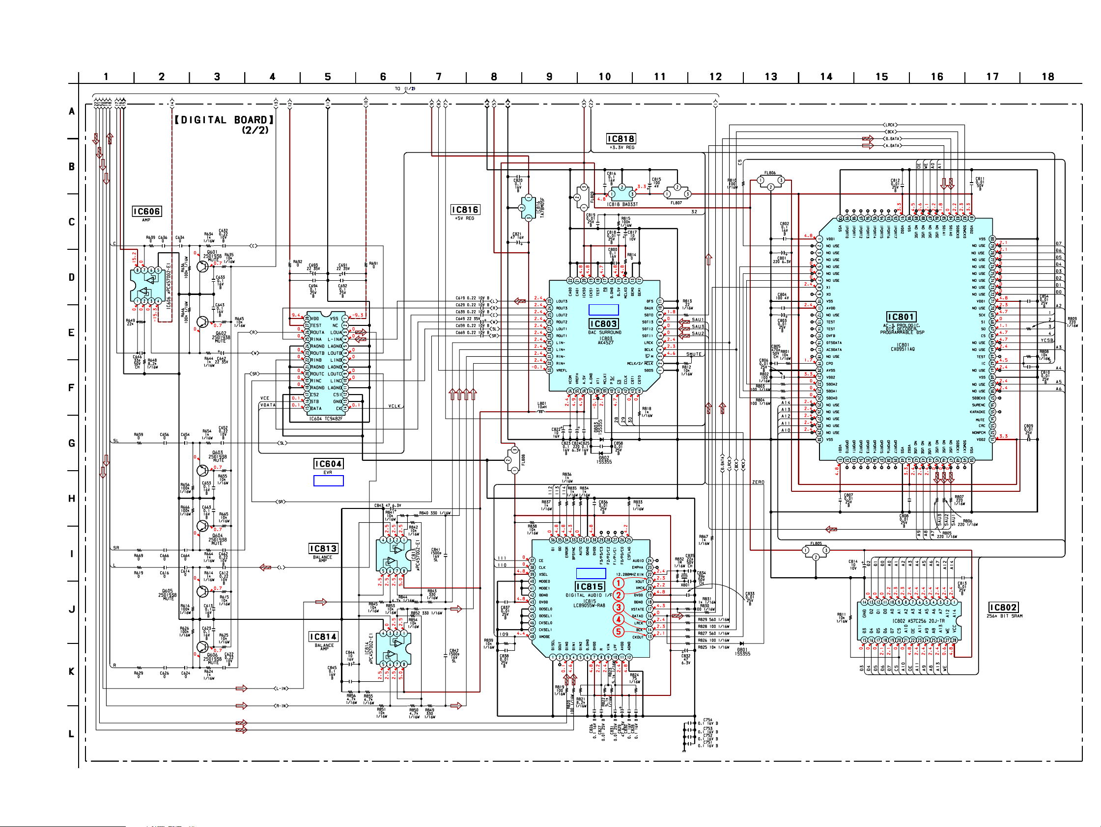
SA-PSD5/WPSD5/SS-SPSD5
2-6. SCHEMATIC DIAGRAM – DIGITAL SECTION (2/2) –
• See page 4 for Waveforms. • See page 21, 22 for IC Block Diagrams.
IC B/D
IC B/D
IC B/D
99
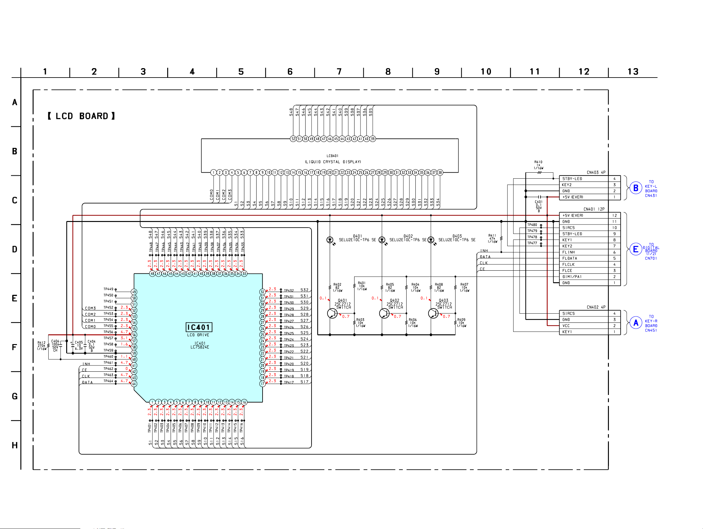
SA-PSD5/WPSD5/SS-SPSD5
2-7. SCHEMATIC DIAGRAM – LCD SECTION –
(Page 12)
(Page 8)
(Page 12)
1010
SA-PSD5/WPSD5/SS-SPSD5
)
)
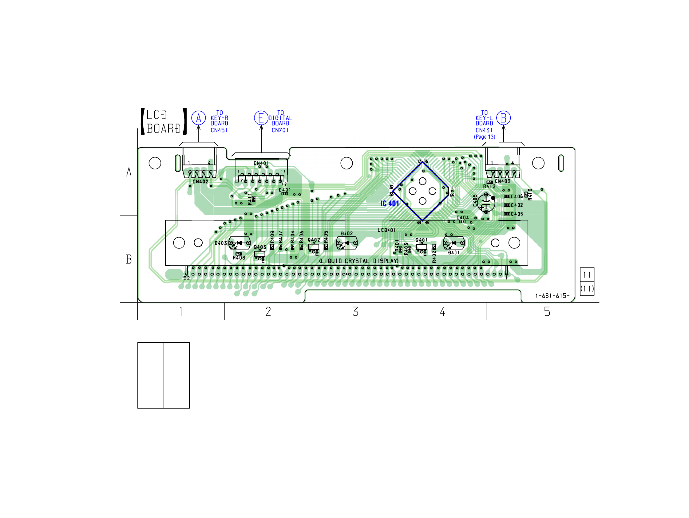
2-8. PRINTED WIRING BOARD – LCD SECTION –
• See page 4 for Circut Borads Lacation.
Page 13
Page 6
• Semiconductor
Location
Ref. No. Location
D401 B-4
D402 B-3
D403 B-2
IC401 A-4
Q401 B-4
Q402 B-3
Q403 B-2
1111
SA-PSD5/WPSD5/SS-SPSD5
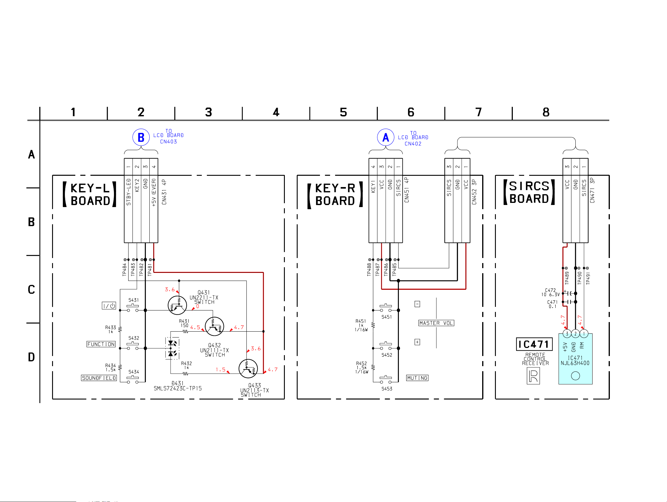
2-9. SCHEMATIC DIAGRAM – KEY SECTION –
(Page 10)
(Page 10)
1212

SA-PSD5/WPSD5/SS-SPSD5
✭
✭
2-10. PRINTED WIRING BO ARD – KEY SECTION –
• See page 4 for Circut Borads Lacation.
✬❖❢❞✤✵✵
✬❖❢❞✤✵✵
1313

SA-PSD5/WPSD5/SS-SPSD5
2-11. SCHEMATIC DIAGRAM – IN/OUT SECTION –
(Page 18)
(Page 8)
(Page 18) (Page 8)
1414
SA-PSD5/WPSD5/SS-SPSD5
OL
✭
✭
❢
✭
2-12. PRINTED WIRING BO ARD – IN/OUT SECTION –
• See page 4 for Circut Borads Lacation.
✬❖❢❞✤✶✴
✬❖❢❞✤✶✴
✬❖❢❞✤✺✭
BASS CONTR
✬❖
❞✤✺
1515

SA-PSD5/WPSD5/SS-SPSD5
2-13. SCHEMATIC DIAGRAM – PRE AMP SECTION –
(Page 8)
(Page 19)
1616
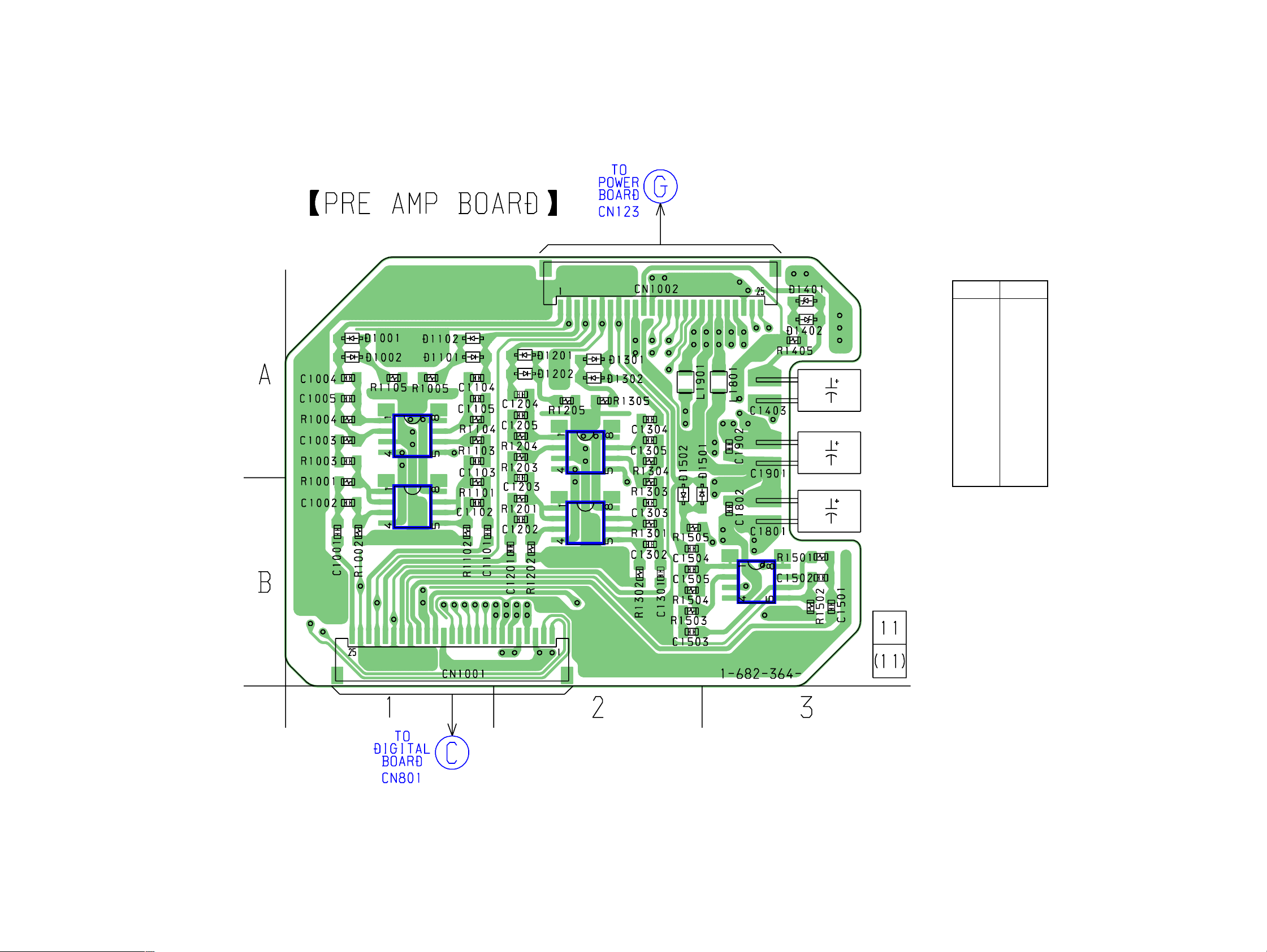
SA-PSD5/WPSD5/SS-SPSD5
2-14. PRINTED WIRING BO ARD – PRE AMP SECTION –
• See page 4 for Circut Borads Lacation.
IC 1002
(Page 20)
• Semiconductor
Location
Ref. No. Location
D1001 A-1
D1002 A-1
D1101 A-1
D1102 A-1
D1201 A-2
D1202 A-2
D1301 A-2
D1302 A-2
D1401 A-3
D1501 B-2
D1502 B-2
IC 1202
IC1001 B-1
IC1002 A-1
IC1201 B-2
IC1202 A-2
IC1401 B-3
IC 1001
(Page 6)
IC 1201
IC 1401
1717
SA-PSD5/WPSD5/SS-SPSD5
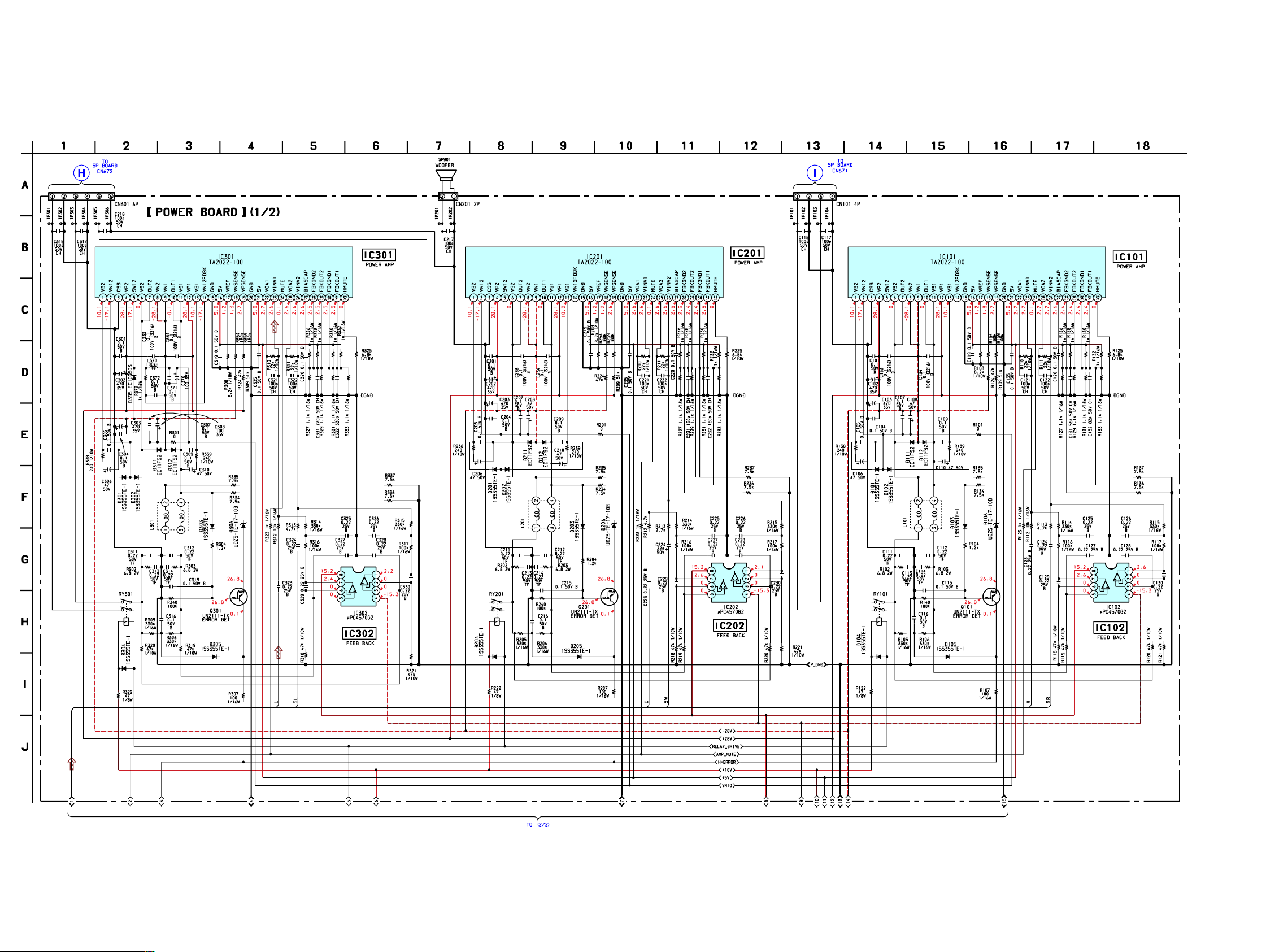
2-15. SCHEMATIC DIAGRAM – POWER SECTION (1/2) –
(Page 14)
(Page 14)
1818
 Loading...