

Page 1
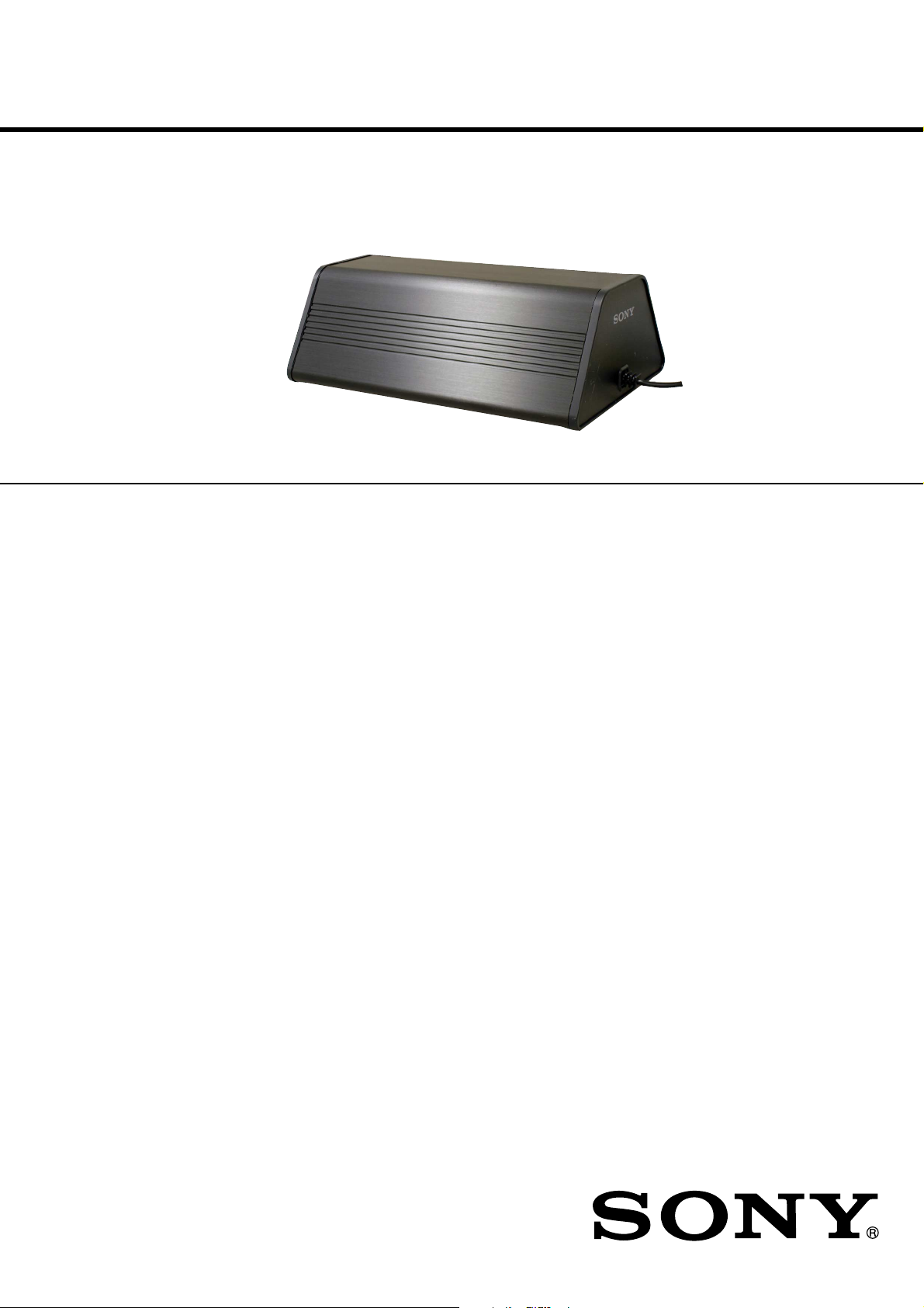
SA-iP001P
SERVICE MANUAL
Ver. 1.0 2006. 12
• SA-iP001P is active subwoofer in CPF-iP001.
SPECIFICATIONS
US Model
Canadian Model
AEP Model
UK Model
TABLE OF CONTENTS
Continuous RMS power output (reference):
15 W (100 Hz, 10% THD)
Speaker units: 70 mm (2 7/8 in) dia.
Dimensions (w/h/d): Approx. 218 × 74 × 131 mm
(8 5/8 × 3 × 5 1/4 in), incl.
projecting parts
Mass: Approx. 1.3 kg (2 lb 14 oz)
Operating temperature: 10°C to 35°C (50°F to 95°F)
Power requirements: AC 120 V , 18W, 50/60Hz
(US, CND)
AC 220 V – 240 V,
18 W, 50/60 Hz
(AEP, UK)
(DC OUT: 12 V, 1.0 A)
Design and specifications are subject to change
without notice.
1. GENERAL ................................................................... 2
2. DIAGRAMS................................................................. 3
2-1. Block Diagram ................................................................ 4
2-2. Printed Wiring Board – POWER Board (Side A) – ....... 5
2-3. Printed Wiring Board – POWER Board (Side B) – ....... 6
2-4. Schematic Diagram – POWER Board (1/2) –................ 7
2-5. Schematic Diagram – POWER Board (2/2) –................ 8
3. EXPLODED VIEWS ................................................. 9
4. ELECTRICAL PARTS LIST .................................. 10
9-887-493-01
2006L02-1
© 2006.12
CRADLE AUDIO SUBWOOFER
Sony Corporation
Home Audio Division
Published by Sony Techno Create Corporation
Page 2
SA-iP001P
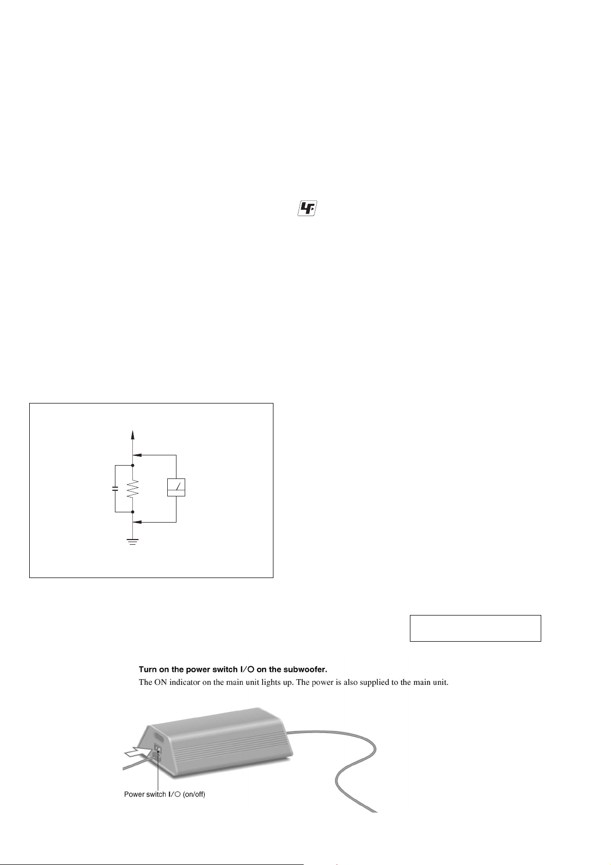
SAFETY CHECK-OUT
After correcting the original service problem, perform the following
safety checks before releasing the set to the customer:
Check the antenna terminals, metal trim, “metallized” knobs, screws,
and all other exposed metal parts for AC leakage. Check leakage as
described below.
LEAKAGE
The AC leakage from any exposed metal part to earth ground and
from all exposed metal parts to any exposed metal part having a
return to chassis, must not exceed 0.5 mA (500 microamperes).
Leakage current can be measured by any one of three methods.
1. A commercial leakage tester , such as the Simpson 229 or RCA
WT -540A. Follow the manufacturers’ instructions to use these
instruments.
2. A battery-operated AC milliammeter. The Data Precision 245
digital multimeter is suitable for this job.
3. Measuring the voltage drop across a resistor by means of a
VOM or battery-operated AC voltmeter . The “limit” indication
is 0.75 V, so analog meters must have an accurate low-voltage
scale. The Simpson 250 and Sanwa SH-63Trd are examples
of a passive VOM that is suitable. Nearly all battery operated
digital multimeters that have a 2V AC range are suitable. (See
Fig. A)
Notes on chip component replacement
• Never reuse a disconnected chip component.
• Notice that the minus side of a tantalum capacitor may be
damaged by heat.
UNLEADED SOLDER
Boards requiring use of unleaded solder are printed with the leadfree mark (LF) indicating the solder contains no lead.
(Caution: Some printed circuit boards may not come printed with
the lead free mark due to their particular size.)
: LEAD FREE MARK
Unleaded solder has the following characteristics.
• Unleaded solder melts at a temperature about 40°C higher than
ordinary solder.
Ordinary soldering irons can be used but the iron tip has to be
applied to the solder joint for a slightly longer time.
Soldering irons using a temperature regulator should be set to
about 350°C.
Caution: The printed pattern (copper foil) may peel away if
the heated tip is applied for too long, so be careful!
• Strong viscosity
Unleaded solder is more viscous (sticky, less prone to flow)
than ordinary solder so use caution not to let solder bridges
occur such as on IC pins, etc.
• Usable with ordinary solder
It is best to use only unleaded solder but unleaded solder may
also be added to ordinary solder.
To Exposed Metal
Parts on Set
AC
0.15 µF
Fig. A. Using an A C v oltmeter to check A C leakage.
1.5 kΩ
Earth Ground
Voltmeter
(0.75 V)
COMPONENTS IDENTIFIED BY MARK 0 OR DOTTED LINE WITH
MARK 0 ON THE SCHEMATIC DIAGRAMS AND IN THE PARTS
LIST ARE CRITICAL TO SAFE OPERATION. REPLACE THESE
COMPONENTS WITH SONY PARTS WHOSE PART NUMBERS
APPEAR AS SHOWN IN THIS MANUAL OR IN SUPPLEMENTS
PUBLISHED BY SONY .
LES COMPOSANTS IDENTIFÉS P AR UNE MARQUE 0 SUR LES
DIAGRAMMES SCHÉMA TIQUES ET LA LISTE DES PIÈCES SONT
CRITIQUES POUR LA SÉCURITÉ DE FONCTIONNEMENT. NE
REMPLACER CES COMPOSANTS QUE PAR DES PIÈSES SONY
DONT LES NUMÉROS SONT DONNÉS DANS CE MANUEL OU
DANS LES SUPPÉMENTS PUBLIÉS PAR SONY.
SECTION 1
GENERAL
SAFETY-RELATED COMPONENT WARNING!!
ATTENTION AU COMPOSANT AYANT RAPPORT
À LA SÉCURITÉ!
This section is extracted from
instruction manual.
2
Page 3
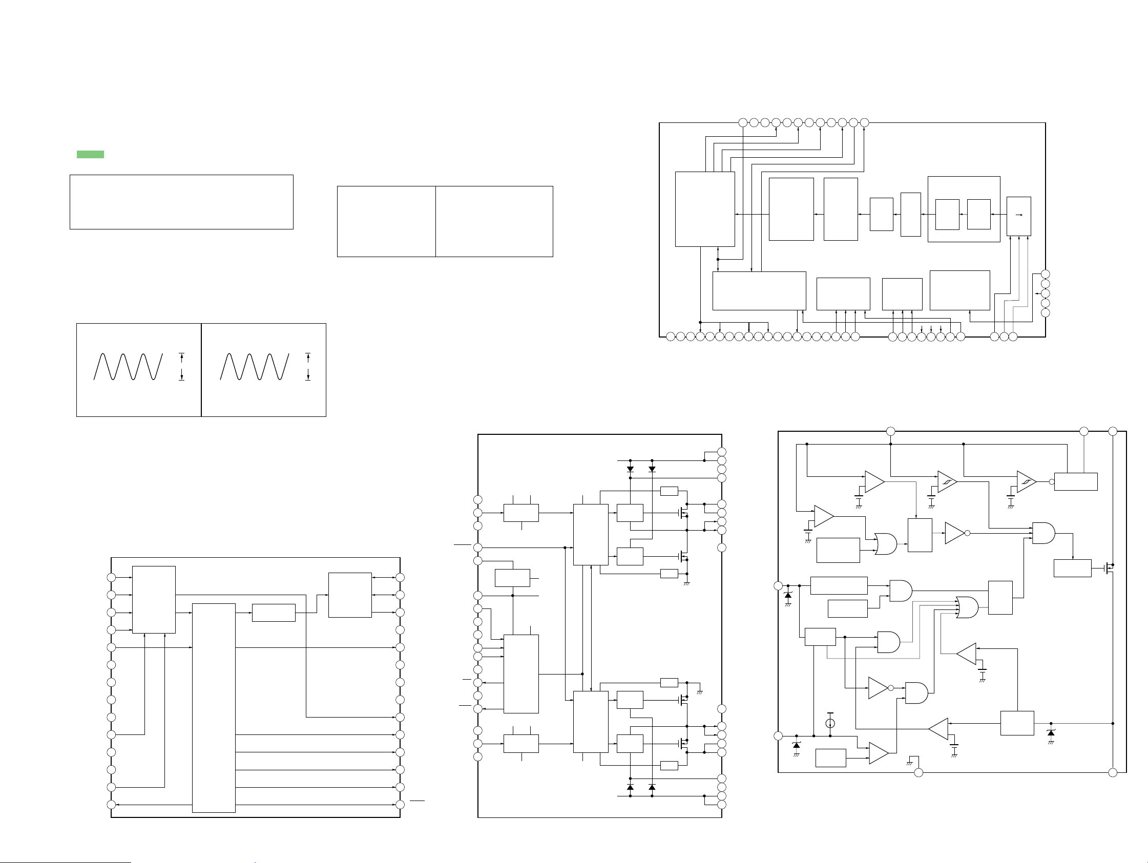
SECTION 2
4 67
LATCH CIRCUIT RESET
COMPARATOR
START–UP CIRCUIT
UVLO
COMPARATOR
OCP THRESHOLD
COMPARATOR
UVLO
COMPARATOR
OVP
COMPARATOR
VUL
VCC (START)/
VCC (STOP)
VCC (STARTUP OFF)/
VCC (STARTUP ON)
START–UP
CIRCUIT
SOFT DRIVE
CIRCUIT
VOVP
THERMAL
SHUTDOWN
CIRCUIT
ZERO CURRENT
DETECTION CIRCUIT
TURN–ON
DEAD TIMER
STANDBY
CIRCUIT
VREF
IF/B
ON WIDTH
TIMER
VTH (OCL)
BURST MODE
OCP THRESHOLD
COMPARATOR
RESTART
TIMER
VTH (BURST LIMIT)
+
–
+
–
+
–
+
–
+
–
+
–
R
S
Q
R
S
Q
GND
1
+
–
3
2
5
Z/C
F/B
SOURCE/OCL
DRAINVINVCC
Q1
DIAGRAMS
SA-iP001P
• Note for Printed Wiring Boards and Schematic Diagrams
Note on Printed Wiring Boards.
• X : parts extracted from the component side.
• Y : parts extracted from the conductor side.
• a : Through hole.
• f : internal component
• : Pattern from the side which enables seeing.
(The other layers' patterns are not indicated.)
Caution:
Pattern face side: Parts on the pattern face side seen from
(Side B) the pattern face are indicated.
Parts face side: Parts on the parts face side seen from
(Side A) the parts face are indicated.
•Waveforms
IC704 qc ( X IN )
1
1.6 Vp-p
IC806 2 ( A )
2
0.5 Vp-p
Note on Schematic Diagrams.
• All capacitors are in µF unless otherwise noted. (p: pF)
50 WV or less are not indicated except for electrolytics
and tantalums.
• All resistors are in Ω and 1/
specified.
4
W or less unless otherwise
• f : internal tolerance.
• C : panel designation.
Note:
The components identified by mark 0 or dotted line with mark 0 are
critical for safety.
Replace only with part
number specified.
Note:
Les composants identifiés
par une marque 0 sont cri-
tiques pour la sécurité.
Ne les remplacer que par une
piéce portant le numéro
spécifié.
• A : B+ Line.
•Voltages are dc with respect to ground under no-signal
conditions.
•Voltages are taken with a VOM (Input impedance 10 MΩ).
Voltage variations may be noted due to normal production tolerances.
• Signal path.
F : AUDIO
IC802 CXD9788AR
PWM
(Secondary Clock System)
1
3
567
2
4
XVSS
VSUBC
VSSR
OUTR2
VDDR
OUTR1
VSSR
XVDD35HPVDDL
XFSOIN
47
46
48
Clock Generator
9
8
10 11
VSSL
VDDL
OUTL2
HPVSSL
HPOUTL1
4445
∆ ∑ Converter
12
13
VSSL
OUTL1
XOVSS
HPOUTL2
15
14
XFSOOUT
HPVDDR30HPOUTR1
424341
40
Interpolator
16
17
DVSS
DVDD
XOVDD
HPVSSR
HPOUTR2
39
Liner
INIT/MUTE
18
19
NSPMUTE
SOFTMUTE
FSOI
38 37
20
PGMUTE
FSOCKO
Gain
Control
Filter
&
LOW
CUT
Filter
Serial Control
23
22
21
SCDT
SCSHIFT
Sampling Rate
Converter
DF2
Clock Generator
(Primary Clock System)
24
26
25
SFLAG
SCLATCH
OVF FLAGL
OVF FLAGR
29
LRCK
BCK
S P
31
DATA
XFSIIN
36
DVDD
TEST
34
33
BFVSS
BFVDD
32
DF1
28
27
INIT
MCKSEL
• IC Block Diagrams
SA-iP001P
5 MHz
49.152 MHz
0.5 V/DIV, 0.1 µsec/DIV 0.1 V/DIV, 50 µsec/DIV
AES3 RX
&
DECODER
IC801 CS8416-CZZR
1
RXP3
RXP2
2
RXP1
3
RXP0
4
RXN
5
VA
6
AGND
7
FILT
8
RST
9
10
RXSEL1
RXSEL0
11
TXSEL1
12
TXSEL0
NV/RERR
13
14
4:2
MUX
DE–EMPHASIS
FILTER
SERIAL
AUDIO
OUTPUT
IC803 CXD9774M
GVDD B36
GVDD
GND
PWM BP
2
GND
3
RESET 4
DREG RTN 5
28
OLRCK
27
OSCLK
26
SDOUT
25
OMCK
24
RMCK
VD
23
DGND
22
VL
21
TX
20
C
19
U
18
RCBL
17
16
96kHz
15
AUDIO
GVDD
DREG 8
DGND
DVDD
DGND
OTW 15
GND
PWM AP
GND
6
M3 7
9
M1 10
M2 11
12
SD 13
14
16
17
18
PWM
RECEIVER
DGND
DIGITAL
REGULATOR
PROTECTION
LOGIC
OT
&
UVP
DVDD DREG
PWM
RECEIVER
DGND
DREG
DREG
GVDD
TIMING
CONTROL
&
PROTECTION
TIMING
CONTROL
&
PROTECTION
DREG
GVDD
GATE
DRIVE
GATE
DRIVE
GATE
DRIVE
GATE
DRIVE
DREG DREG
DVDD
1
OCH
OCL
OCL
OCH
34
32
31
30
29
28
27
26
25
24
23
22
21
20
19
GVDD B35
GND
BST B33
PVDD B
PVDD B
OUT B
OUT B
GND
GND
OUT A
OUT A
PVDD A
PVDD A
BST A
GND
GVDD A
GVDD A
IC901 MR4010-7103
33
Page 4
SA-iP001P
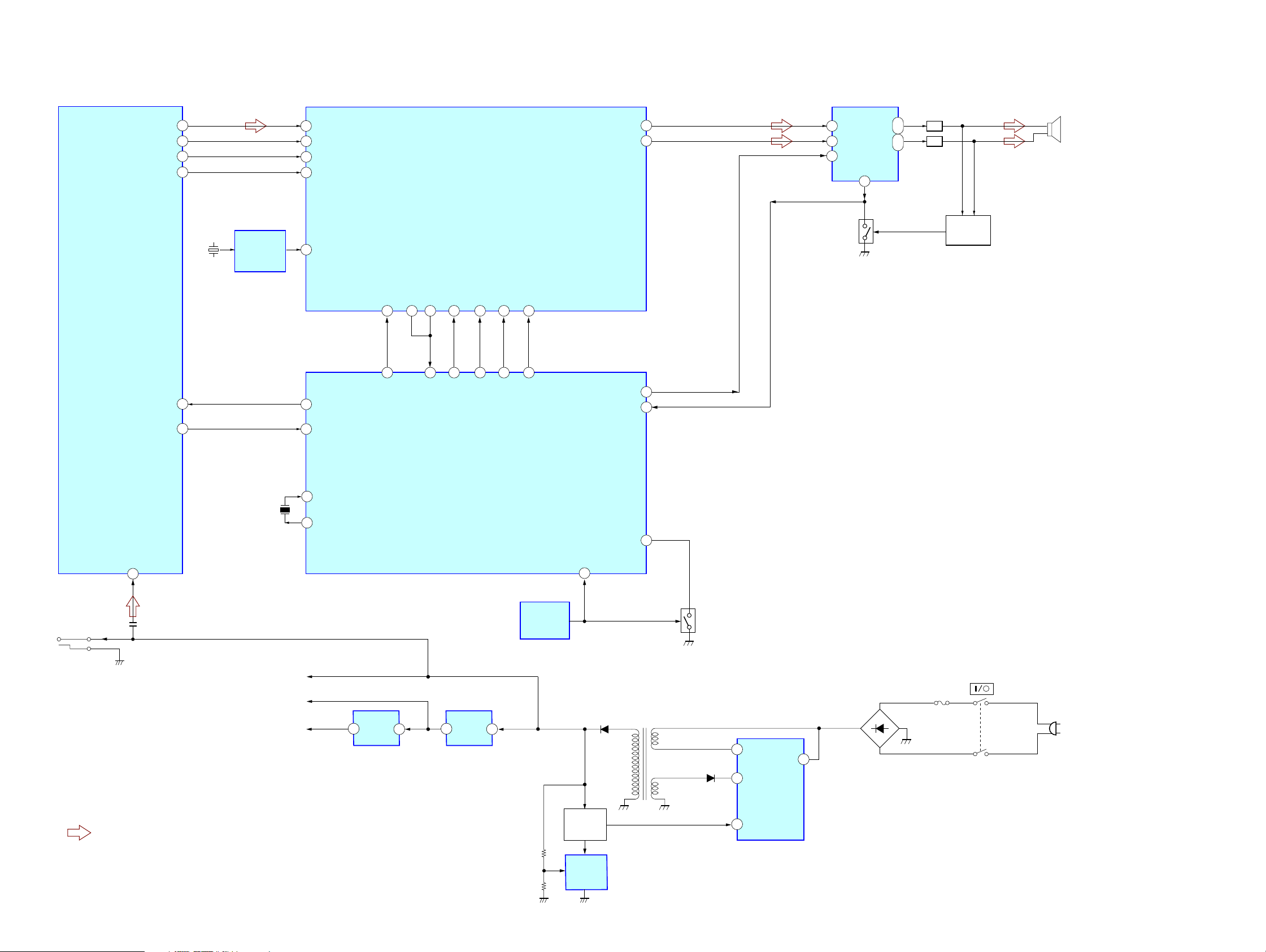
2-1. BLOCK DIAGRAM
IC803
POWER DRIVER
IC801
192kHz DIGITAL AUDIO
INTERFACE RECEIVER
NV/RERR
SDOUT
OLRCK
OSCLK
RMCK
RST
26
28
27
24
9
14
X801
49.152MHZ
IC806
OSC
31
29
30
36
48
56
55
DATA
LRCK
BCK
XFSI_IN
XFSO_IN
DIR_RST
DIR_ERR
INIT
27
48
DAMP_INT
FLAG_L_OVF24OVR_FLAGR
25
42
OVERFLOW1
IC802
S-MASTER
PROCESSOR
SCLATCH
23
45
DAMP_LATCH1
SCSHIFT
22
100
DAMP_SHIFT
SCDT
21
99
DAMP_SCD
SOFTMUTE
19
49
DAMP_SOFTMUTE
OUT1
OUT2
DRIVE_RST (EN)
DRIVE_OCP (DIAG)
11
9
40
41
2
PWMBP
17
PWMAP
4
RESET
Q801
PROTECT
SWITCH
13
OUTB
OUTA
SD
29
30
25
26
LPF
LPF
Q802, 803
OVER LOAD
DETECT
SP1
SUB WOOFER
DC OUT
• Signal Path
: AUDIO
4
RXP0
X701
5MHz
+B 12V
+B 3.3V
+B 1.8V
13 X-IN
11 X-OUT
IC805
4
+1.8V REG
IC704
SYSTEM CONTROL
10
RESET
AC_CUT
18
IC701
RESET
T901
POWER TRANSFORMER
IC804
5
5
+3.3V REG
4
D907
Q701
RESET
D903
6
4
DRAIN
VCC
VIN
S901
D901
7
F901
AC IN
IC901
POWER
ERROR
AMP
PC901
2 FB
SWITCHING
CONVERTER
SA-iP001P
IC902
SHUNT
REG
44
Page 5
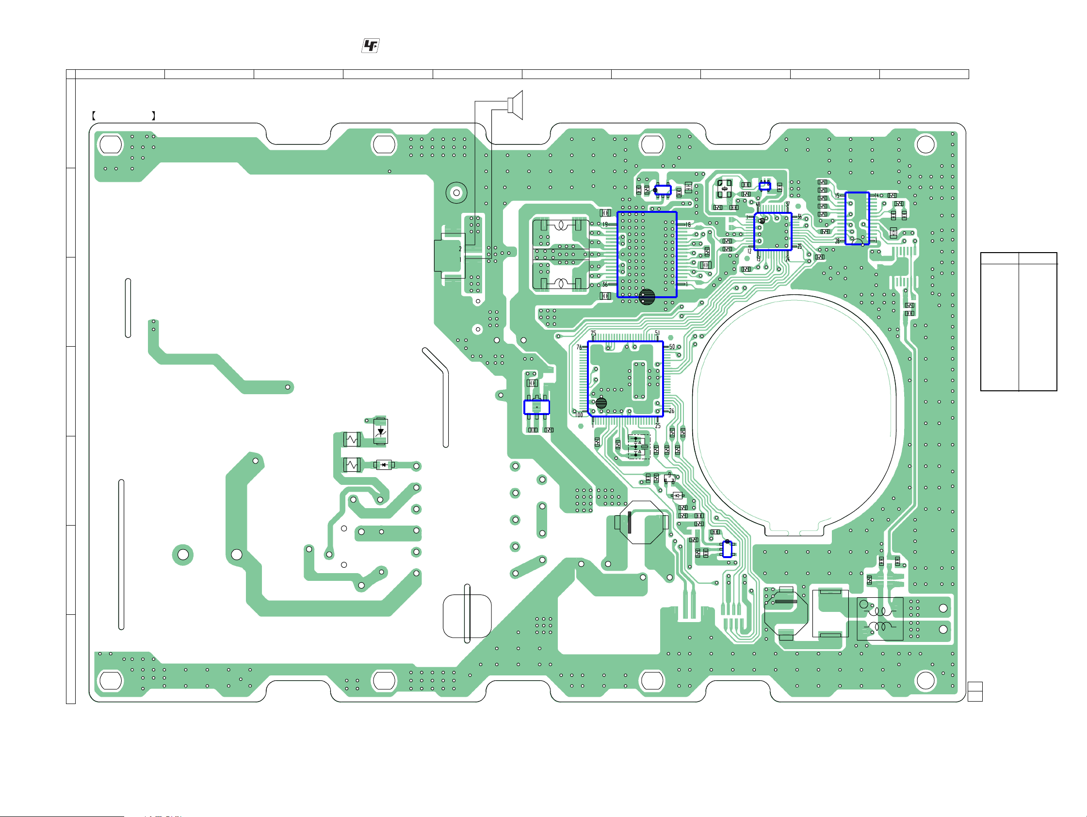
SA-iP001P
2-2. PRINTED WIRING BOARD – POWER BOARD (SIDE A) –
1
POWER BOARD (SIDE A)
A
B
C
2
3 4 5 6 7
:Uses unleaded solder.
CP2
CN801
SP1
SUB WOOFER
L801
C829
C830
IC704
C810
IC803
IC805
5
1
R830
8
C811
4
C812
3
R804
X801
C841
C840
R803
IC806
3
4
1
5
C818
R816
R815
R813
R812
R811
IC802
R846
R841
R845
C825
R863
9 10
IC801
R808
R822
R819
C802
R801
C803
C801
• Semiconductor
Location
Ref. No.
D701 E-7
D903 E-4
Location
D904 D-4
R823
C806
IC701 F-8
IC704 D-7
IC801 B-9
IC802 B-8
IC803 C-7
IC804 D-6
IC805 B-7
IC806 B-8
C809
D
4
5
Q701 E-7
IC804
3
R829
R716
R721
X701
L902
C712
R708
R706
R712
Q701
R705
R704
R713
E
R715
R714
D701
R722
C703
R701
R720
C701
3
1
C702
5
IC701
4
L903
TH902
C920
C922
R921
L901
1
R904
E
R903
D904
D903
C813
F
G
SA-iP001P
1-869-196-
(12)
55
12
Page 6

SA-iP001P
2-3. PRINTED WIRING BOARD – POWER BOARD (SIDE B) –
3 4 5 6 7
R806
C815
C816
C820
C814
C823
R862
R807
C821
C817
C822
R825
R833
C807
2
D801
D802
R814
C805
C804
C854
R817
1
A
POWER BOARD (SIDE B)
B
R826
C
D
E
R861
R844
C826
:Uses unleaded solder.
C827
R843
R821
R809
R810
R820
D805
R711
R707
R731
R730
R710
C704
C836
R717
C710
C833
C832
C835
R832
R850
R849
R831
R703
R724
C834
C831
C711
R914
R901
C918
C819
R915
C838
C837
IC902
R912
R913
C917
R916
R910
POWER TRANSFORMER
R852
R851
R854
R853
E
Q802
E
Q801
T901
R911
R855
R175
C849
C850
C844
C919
C845
C851
C848
R858
R860
E
Q803
R859
R857
C842
C843
C847
C846
R856
PC901
D905
D906
R907
R906
C909
R905
C910
CN901
C911
R908
R909
C908
8
S901
1
2
9 10
AC IN
R918
C901
LF901
11
FH901
F901
C904
FH902
• Semiconductor
Location
Ref. No.
D801 C-2
D802 C-2
D805 C-4
D901 D-9
D902 F-8
D905 D-7
D906 E-7
D907 G-5
D908 F-9
D909 G-8
D910 F-9
D911 F-9
Location
R902
C902
D901
TH901
C903
F
DC OUT
G
SA-iP001P
CN902
C916
C915
C914
D907
C912
66
C913
C907
D902
2
D909
7
IC901
4
IC901 F-8
IC902 D-6
6
5
3
1
D910
D911
D908
C906
Q801 D-7
Q802 C-7
Q803 C-7
C905
12
1-869-196-
(12)
Page 7

SA-iP001P
2-4. SCHEMATIC DIAGRAM – POWER BOARD (1/2) –
R703
47k
R717
10k
C711
10
R724
47k
SCDT
SCSHIFT
• See page 3 for Waveforms.
C704
0.1
IC704
M30620MCP
-A44GPU0
SYSTEM CONTROL
R715
R714
R713
R712
R711
R710
R707
100
100
100
100
47
47
DIR_RST
DIR_ERR
SOFTMUTE
INIT
SCLATCH
10k
OVF
SD
EN
INIT
SCDT
SCSHIFT
SCLATCH
SOFTMUTE
OVF
EN
SD
DIR_RST
DIR_ERR
INIT
SCDT
SCSHIFT
SCLATCH
SOFTMUTE
OVF
EN
SD
DIR_RST
DIR_ERR
GND
3.3V
12V
POWER
BOARD
(2/2)
(Page 8)
SA-iP001P
R716
10k
R721
100
X701
5MHz
C710
10
R708
10k
R730
4.7k
R731
4.7k
IC701
PST3629NR
RESET
C702
0.22
C701
0.1
R722
10k
R720
4.7k
R706
47k
C712
0.1
Q701
2SC4154
RESET
D701
1SS355WTE-17
R704
47k
R705
100k
R701
10k
C703
0.22
77
Page 8

SA-iP001P
2-5. SCHEMATIC DIAGRAM – POWER BOARD (2/2) –
R825
R826
R823
C806
D802
1SS355WTE-17
D801
1SS355WTE-17
C803
10
C807
0.01
C854
0.01
C801
0.022
R801
1k
C802
0.001
R819
47k
0
0
0
0
R833
15
IC801
CS8416-CZZR
192kHz DIGITAL AUDIO
INTERFACE RECEIVER
R816
• See page 3 for Waveforms. • See page 3 for IC Block Diagrams.
ER
POW
BOARD
(1/2)
(Page 7)
SCLATCH
SCSHIFT
C810
1
C818
SOFTMUTE
SCDT
R863
R862
10k
10k
IC802
CXD9788AR
S-MASTER
PROCESSOR
C816
0.1
TC7SHU04FU
0.1
C823
C817
IC806
OSC
0.1
C822
10
C821
0.1
R861
10k
IC B/D
0.1
R806
100
C840
4p
C841
X801
49.152MHz
R803
330
R804
1M
IC B/D
47k
R815
47k
R808
100
C804
10
R811
R812
R813
R814
C805
DIR_ERR
R822
10k
0.1
DIR_RST
INIT
R817
47k
47k
47k
47k
47k
3.3V
GND
C814
0.1
C815
0.1
R807
10k
C811
C812
10
0.01
IC805
TK11118CSCL-G
+1.8V REG
R830
10k
OVF
C820
0.1
C809
4p
12V
SD
EN
R859
IC B/D
Q801
2SC4154
PROTECT
SWITCH
C832
470p
C831
0.047
C834
0.047
C833
470p
C836
470p
R809
C835
470p
1k
L801
10uH
R850
2.2
DBE
R849
2.2
R832
2.2
R860
100k
IC803
CXD9774M
C830
POWER DRIVER
1
16V
R841
100
R821
10k
C825
1
16V
R843
10k
C826
1
16V
R844
10k
R845
10k
C827
1
R846
100
10
IC804
TK11233CUCB-G
+3.3V REG
R829
C813
0.01
10k
C851
4.7
R831
2.2
C829
1
C837
R851
1
C838
R852
1
10k
D805
UDZW-TE17-2.7B
10k
C819
2200
R853
10k
10k
R854
10k
R820
3.3k
Q802
2SA1602
OVER LOAD DETECT
C850
4.7
R856
R810
3.3k
C848
0.1
C844
0.1
100k
16V
Q803
2SA1602
OVER LOAD DETECT
R858
100k
R857
100k
C849
0.001
C845
0.001
C842
C846
0.0022
0.0022
C843
C847
0.0022
0.0022
R855
R175
4.7
4.7
CN801
2P
SP1
SUB WOOFER
AC IN
S901
I/O
CN901
2P
FH901
F901
T1AL
250V
FH902
R918
IC901
MR4010-7103
POWER SWITCHING
CONVERTER
IC B/D
TH901
D3SB60F
R907
10k
C910
47p
M22007C
D901
C906
100
400V
D909
PTZ-TE25-22
D908
PTZ-TE25-22
C909
0.001
R906
20k
05NU42-TPA2
0.33 2W
C908
220
35V
D910
PTZ-TE25-22
R904
150
0.5W
D904
PTZ-TE25-18B
C911
0.0022
M1FL20U-4063
C907
560p
2kV
R902
D902
R903
0.5W
D905
2.2
R905
10k
D903
M1FL20U-4063
R908
1k
R909
4.7k
LF901
C902
C901
0.1
1M
275V
0.1
275V
M1FL20U-4063
D911
C903
220p
250V
C904
220p
250V
C905
220p
250V
C913
100p
250V
T901
POWER
TRANSFORMER
D906
UDZW-TE17-8.2B
C919
470p
250V
PC901
TLP421F(D4-GR)
D907
D10SC6M
IC902
TA76L431S
SHUNT REG
R910
3.3k
R911
C920
0.1
L902
L903
R901
R916
10k
R915
8.2k
R912
4.7k
68uH
C914
470
16V
0
TH902
SMD150/33
C915
220p
4.7uH
C912
2200
16V
R914
4.7k
C918
0.01
C917
R913
0.0033
1k
2.2k
L901
0uH
C922
0.1
C916
220p
R921
CN902
2P
DC OUT
0
SA-iP001P
88
Page 9

SECTION 3
EXPLODED VIEWS
SA-iP001P
NOTE:
• -XX and -X mean standardized parts, so they
may have some difference from the original
one.
• Items marked “*” are not stocked since they
are seldom required for routine service.
Some delay should be anticipated when
ordering these items.
• The mechanical parts with no reference
number in the exploded views are not supplied.
10
F901
#1
9
#2
7
•Accessories are given in the last of the
electrical parts list.
• Abbreviation
CND : Canadian model
#4
#1
#1
not supplied
9
#2
8
not
supplied
#1
#1
not supplied
The components identified by
mark 0 or dotted line with mark
0 are critical for safety.
Replace only with part number
specified.
Les composants identifiés par une
marque 0 sont critiques pour la
sécurité.
Ne les remplacer que par une
piéce portant le numéro spécifié.
#4
SP1
11
not supplied
#1
6
#1
6
not supplied
5
not
supplied
not supplied
12
#3
#1
13
not supplied
4
3
S901
not supplied
2
#1
1
#1
Ref. No. Part No. Description Remark Ref. No. Part No. Description Remark
1 X-2109-404-1 COVER (JACK) ASSY
2 X-2109-401-1 BRACKET (SIDE) (L) ASSY
3 2-667-935-11 CASE (L), SIDE
* 4 3-703-244-00 BUSHING (2104), CORD
0 5 1-832-383-11 CORD, POWER (AEP)
0 5 1-832-965-11 CORD, POWER (US, CND)
0 5 1-832-966-11 CORD, POWER (UK)
6 2-667-948-01 FOOT
7 X-2109-403-1 PLATE ASSY, BOTTOM
8 A-1193-778-A POWER BOARD, COMPLETE
9 X-2109-934-1 SPACER ASSY
10 2-661-193-11 CASE, TOP
#1
14
#1
#1
11 X-2109-400-1 PLATE ASSY, INNER
12 X-2109-402-1 BRACKET (SIDE) (R) ASSY
13 2-667-936-11 CASE (R), SIDE
14 1-831-587-11 CORD WITH DC PLUG
15 1-500-497-21 FILTER, CLAMP (FERRITE CORE)
0F901 1-576-225-51 FUSE (H.B.C.) (T1AL/250V)
0S901 1-771-124-21 SWITCH, POWER (I/O)
SP1 1-826-330-21 LOUDSPEAKER (8cm)
#1 7-685-646-79 SCREW +BVTP 3X8 TYPE2 IT-3
#2 7-685-649-79 SCREW +BVTP 3X14 TYPE2 IT-3
#3 7-685-132-19 SCREW +P 2.6X5 TYPE2 NON-SLIT
#4 7-685-659-79 SCREW +BVTP 4X8 TYPE2 IT-3
15
9
Page 10

SA-iP001P
POWER
SECTION 4
ELECTRICAL PARTS LIST
NOTE:
• Due to standardization, replacements in the
parts list may be different from the parts
specified in the diagrams or the components
used on the set.
• -XX and -X mean standardized parts, so they
may have some difference from the original
one.
• RESISTORS
All resistors are in ohms.
METAL: Metal-film resistor.
METAL OXIDE: Metal oxide-film resistor.
F: nonflammable
• Items marked “*” are not stocked since they
are seldom required for routine service.
Some delay should be anticipated when
ordering these items.
Ref. No. Part No. Description Remark Ref. No. Part No. Description Remark
A-1193-778-A POWER BOARD, COMPLETE
**********************
7-685-871-01 SCREW +BVTT 3X6 (S)
7-685-872-01 SCREW +BVTT 3X8 (S)
< CAPACITOR >
C701 1-107-826-11 CERAMIC CHIP 0.1uF 10% 16V
C702 1-115-467-11 CERAMIC CHIP 0.22uF 10% 10V
C703 1-115-467-11 CERAMIC CHIP 0.22uF 10% 10V
C704 1-107-826-11 CERAMIC CHIP 0.1uF 10% 16V
C710 1-165-989-11 CERAMIC CHIP 10uF 10% 6.3V
C711 1-165-989-11 CERAMIC CHIP 10uF 10% 6.3V
C712 1-107-826-11 CERAMIC CHIP 0.1uF 10% 16V
C801 1-164-227-11 CERAMIC CHIP 0.022uF 10% 25V
C802 1-115-416-11 CERAMIC CHIP 0.001uF 5% 25V
C803 1-165-989-11 CERAMIC CHIP 10uF 10% 6.3V
C804 1-165-989-11 CERAMIC CHIP 10uF 10% 6.3V
C805 1-107-826-11 CERAMIC CHIP 0.1uF 10% 16V
C806 1-216-864-11 SHORT CHIP 0
C807 1-162-970-11 CERAMIC CHIP 0.01uF 10% 25V
C809 1-165-989-11 CERAMIC CHIP 10uF 10% 6.3V
C810 1-112-298-91 CERAMIC CHIP 1uF 10% 16V
C811 1-165-989-11 CERAMIC CHIP 10uF 10% 6.3V
C812 1-162-970-11 CERAMIC CHIP 0.01uF 10% 25V
C813 1-162-970-11 CERAMIC CHIP 0.01uF 10% 25V
C814 1-107-826-11 CERAMIC CHIP 0.1uF 10% 16V
C815 1-107-826-11 CERAMIC CHIP 0.1uF 10% 16V
C816 1-107-826-11 CERAMIC CHIP 0.1uF 10% 16V
C817 1-107-826-11 CERAMIC CHIP 0.1uF 10% 16V
C818 1-107-826-11 CERAMIC CHIP 0.1uF 10% 16V
C819 1-128-951-21 ELECT 2200uF 20% 16V
C820 1-107-826-11 CERAMIC CHIP 0.1uF 10% 16V
C821 1-107-826-11 CERAMIC CHIP 0.1uF 10% 16V
C822 1-165-989-11 CERAMIC CHIP 10uF 10% 6.3V
C823 1-107-826-11 CERAMIC CHIP 0.1uF 10% 16V
C825 1-112-298-91 CERAMIC CHIP 1uF 10% 16V
C826 1-112-298-91 CERAMIC CHIP 1uF 10% 16V
C827 1-112-298-91 CERAMIC CHIP 1uF 10% 16V
C829 1-112-298-91 CERAMIC CHIP 1uF 10% 16V
C830 1-112-298-91 CERAMIC CHIP 1uF 10% 16V
C831 1-104-760-11 CERAMIC CHIP 0.047uF 10% 50V
• SEMICONDUCTORS
In each case, u: µ, for example:
uA... : µA... uPA... : µPA...
uPB... : µPB... uPC... : µPC...
uPD... : µPD...
• CAPACITORS
uF: µF
• COILS
uH: µH
• Abbreviation
CND : Canadian model
C834 1-104-760-11 CERAMIC CHIP 0.047uF 10% 50V
C835 1-164-315-11 CERAMIC CHIP 470PF 5% 50V
C836 1-164-315-11 CERAMIC CHIP 470PF 5% 50V
C837 1-131-704-11 FILM 1uF 5% 50V
C838 1-131-704-11 FILM 1uF 5% 50V
C840 1-162-909-11 CERAMIC CHIP 4PF 0.25PF 50V
C841 1-162-909-11 CERAMIC CHIP 4PF 0.25PF 50V
C842 1-162-966-11 CERAMIC CHIP 0.0022uF 10% 50V
C843 1-162-966-11 CERAMIC CHIP 0.0022uF 10% 50V
C844 1-107-826-11 CERAMIC CHIP 0.1uF 10% 16V
C845 1-115-416-11 CERAMIC CHIP 0.001uF 5% 25V
C846 1-162-966-11 CERAMIC CHIP 0.0022uF 10% 50V
C847 1-162-966-11 CERAMIC CHIP 0.0022uF 10% 50V
C848 1-107-826-11 CERAMIC CHIP 0.1uF 10% 16V
C849 1-115-416-11 CERAMIC CHIP 0.001uF 5% 25V
C850 1-117-720-11 CERAMIC CHIP 4.7uF 10V
C851 1-117-720-11 CERAMIC CHIP 4.7uF 10V
C854 1-162-970-11 CERAMIC CHIP 0.01uF 10% 25V
0 C901 1-165-528-11 MYLAR 0.1uF 10 275V
0 C902 1-165-528-11 MYLAR 0.1uF 10 275V
0 C903 1-113-896-11 CERAMIC 220PF 10% 250V
0 C904 1-113-896-11 CERAMIC 220PF 10% 250V
0 C905 1-113-896-11 CERAMIC 220PF 10% 250V
0 C906 1-112-684-21 ELECT (BLOCK) 100uF 20% 400V
0 C907 1-100-448-51 CAP, HIGH-VOLTAGE CERAMIC 560PF
0 C908 1-107-894-11 ELECT 220uF 20% 35V
0 C909 1-115-416-11 CERAMIC CHIP 0.001uF 5% 25V
0 C910 1-162-923-11 CERAMIC CHIP 47PF 5% 50V
0 C911 1-162-966-11 CERAMIC CHIP 0.0022uF 10% 50V
C912 1-128-951-21 ELECT 2200uF 20% 16V
0 C913 1-117-693-11 CERAMIC 100PF 10% 250V
C914 1-165-729-31 ELECT 470uF 20% 16V
C915 1-164-816-11 CERAMIC CHIP 220PF 2% 50V
C916 1-164-816-11 CERAMIC CHIP 220PF 2% 50V
C917 1-162-967-11 CERAMIC CHIP 0.0033uF 10% 50V
C918 1-162-970-11 CERAMIC CHIP 0.01uF 10% 25V
0 C919 1-113-900-11 CERAMIC 470PF 10% 250V
C920 1-107-826-11 CERAMIC CHIP 0.1uF 10% 16V
C922 1-107-826-11 CERAMIC CHIP 0.1uF 10% 16V
The components identified by
mark 0 or dotted line with mark
0 are critical for safety.
Replace only with part number
specified.
Les composants identifiés par une
marque 0 sont critiques pour la
sécurité.
Ne les remplacer que par une
piéce portant le numéro spécifié.
When indicating parts by reference
number, please include the board
name.
< CONNECTOR >
C832 1-164-315-11 CERAMIC CHIP 470PF 5% 50V
C833 1-164-315-11 CERAMIC CHIP 470PF 5% 50V
10
CN801 1-778-638-21 PIN, CONNECTOR (PC BOARD) 2P
0 CN901 1-564-321-00 PIN, CONNECTOR (3.96mm PITCH) 2P
Page 11

SA-iP001P
POWER
Ref. No. Part No. Description Remark Ref. No. Part No. Description Remark
CN902 1-564-320-00 PIN, CONNECTOR (3.96mm PITCH) 2P
R705 1-216-845-11 METAL CHIP 100K 5% 1/10W
< DIODE >
D701 6-501-193-01 DIODE 1SS355WTE-17
D801 6-501-193-01 DIODE 1SS355WTE-17
D802 6-501-193-01 DIODE 1SS355WTE-17
D805 6-501-160-01 DIODE UDZW-TE17-2.7B
0 D901 8-719-510-51 DIODE D3SB60F
0 D902 8-719-058-74 DIODE 05NU42-TPA2
0 D903 8-719-080-75 DIODE M1FL20U-4063
0 D904 8-719-076-95 DIODE PTZ-TE25-18B
0 D905 8-719-080-75 DIODE M1FL20U-4063
0 D906 6-501-172-01 DIODE UDZW-TE17-8.2B
D907 8-719-510-09 DIODE D10SC6M
0 D908 8-719-079-55 DIODE PTZ-TE25-22
0 D909 8-719-079-55 DIODE PTZ-TE25-22
0 D910 8-719-079-55 DIODE PTZ-TE25-22
0 D911 8-719-080-75 DIODE M1FL20U-4063
< FUSE HOLDER >
0 FH901 1-533-217-41 HOLDER, FUSE
0 FH902 1-533-217-41 HOLDER, FUSE
< IC >
IC701 6-701-680-01 IC PST3629NR
IC704 6-807-280-01 IC M30620MCP-A44GPU0
IC801 6-709-054-01 IC CS8416-CZZR
IC802 6-705-979-01 IC CXD9788AR
IC803 6-704-802-01 IC CXD9774M
IC804 6-702-316-11 IC TK11233CUCB-G
IC805 6-702-300-01 IC TK11118CSCL-G
IC806 6-706-492-01 IC TC7SHU04FU (T5RSOJF)
0 IC901 6-708-175-01 IC MR4010-7103
IC902 6-707-743-01 IC TA76L431S (TPE6, Q)
< COIL >
L801 1-457-191-11 INDUCTOR 10uH
L901 1-400-101-21 COIL, COMMON MODE CHOKE
L902 1-457-190-21 INDUCTOR 4.7uH
L903 1-457-192-21 INDUCTOR 68uH
< LINE FILTER >
R706 1-216-841-11 METAL CHIP 47K 5% 1/10W
R707 1-216-833-11 METAL CHIP 10K 5% 1/10W
R708 1-216-833-11 METAL CHIP 10K 5% 1/10W
R710 1-216-805-11 METAL CHIP 47 5% 1/10W
R711 1-216-805-11 METAL CHIP 47 5% 1/10W
R712 1-216-809-11 METAL CHIP 100 5% 1/10W
R713 1-216-809-11 METAL CHIP 100 5% 1/10W
R714 1-216-809-11 METAL CHIP 100 5% 1/10W
R715 1-216-809-11 METAL CHIP 100 5% 1/10W
R716 1-216-833-11 METAL CHIP 10K 5% 1/10W
R717 1-216-833-11 METAL CHIP 10K 5% 1/10W
R720 1-216-829-11 METAL CHIP 4.7K 5% 1/10W
R721 1-216-809-11 METAL CHIP 100 5% 1/10W
R722 1-216-833-11 METAL CHIP 10K 5% 1/10W
R724 1-216-841-11 METAL CHIP 47K 5% 1/10W
R730 1-216-829-11 METAL CHIP 4.7K 5% 1/10W
R731 1-216-829-11 METAL CHIP 4.7K 5% 1/10W
R801 1-216-821-11 METAL CHIP 1K 5% 1/10W
R803 1-216-815-11 METAL CHIP 330 5% 1/10W
R804 1-216-857-11 METAL CHIP 1M 5% 1/10W
R806 1-216-809-11 METAL CHIP 100 5% 1/10W
R807 1-216-833-11 METAL CHIP 10K 5% 1/10W
R808 1-216-809-11 METAL CHIP 100 5% 1/10W
R809 1-216-821-11 METAL CHIP 1K 5% 1/10W
R810 1-216-827-11 METAL CHIP 3.3K 5% 1/10W
R811 1-216-841-11 METAL CHIP 47K 5% 1/10W
R812 1-216-841-11 METAL CHIP 47K 5% 1/10W
R813 1-216-841-11 METAL CHIP 47K 5% 1/10W
R814 1-216-841-11 METAL CHIP 47K 5% 1/10W
R815 1-216-841-11 METAL CHIP 47K 5% 1/10W
R816 1-216-841-11 METAL CHIP 47K 5% 1/10W
R817 1-216-841-11 METAL CHIP 47K 5% 1/10W
R819 1-216-841-11 METAL CHIP 47K 5% 1/10W
R820 1-216-827-11 METAL CHIP 3.3K 5% 1/10W
R821 1-216-833-11 METAL CHIP 10K 5% 1/10W
R822 1-216-833-11 METAL CHIP 10K 5% 1/10W
R823 1-216-864-11 SHORT CHIP 0
R825 1-216-864-11 SHORT CHIP 0
R826 1-216-864-11 SHORT CHIP 0
R829 1-216-833-11 METAL CHIP 10K 5% 1/10W
0 LF901 1-457-254-11 COIL,LINE FILTER (SS21V-050360)
< PHOTO COUPLER >
0 PC901 6-600-438-01 IC TLP421F (D4-GR)
< TRANSISTOR >
Q701 8-729-602-21 TRANSISTOR 2SC4154-F
Q801 8-729-602-21 TRANSISTOR 2SC4154-F
Q802 8-729-602-36 TRANSISTOR 2SA1602-F
Q803 8-729-602-36 TRANSISTOR 2SA1602-F
< RESISTOR >
R175 1-216-793-11 METAL CHIP 4.7 5% 1/10W
R701 1-216-833-11 METAL CHIP 10K 5% 1/10W
R703 1-216-841-11 METAL CHIP 47K 5% 1/10W
R704 1-216-841-11 METAL CHIP 47K 5% 1/10W
R830 1-216-833-11 METAL CHIP 10K 5% 1/10W
R831 1-216-789-11 METAL CHIP 2.2 5% 1/10W
R832 1-216-789-11 METAL CHIP 2.2 5% 1/10W
R833 1-216-799-11 METAL CHIP 15 5% 1/10W
R841 1-216-809-11 METAL CHIP 100 5% 1/10W
R843 1-216-833-11 METAL CHIP 10K 5% 1/10W
R844 1-216-833-11 METAL CHIP 10K 5% 1/10W
R845 1-216-833-11 METAL CHIP 10K 5% 1/10W
R846 1-216-809-11 METAL CHIP 100 5% 1/10W
R849 1-216-789-11 METAL CHIP 2.2 5% 1/10W
R850 1-216-789-11 METAL CHIP 2.2 5% 1/10W
R851 1-216-833-11 METAL CHIP 10K 5% 1/10W
R852 1-216-833-11 METAL CHIP 10K 5% 1/10W
R853 1-216-833-11 METAL CHIP 10K 5% 1/10W
R854 1-216-833-11 METAL CHIP 10K 5% 1/10W
R855 1-216-793-11 METAL CHIP 4.7 5% 1/10W
11
Page 12

SA-iP001P
POWER
Ref. No. Part No. Description Remark
R856 1-216-845-11 METAL CHIP 100K 5% 1/10W
R857 1-216-845-11 METAL CHIP 100K 5% 1/10W
R858 1-216-845-11 METAL CHIP 100K 5% 1/10W
R859 1-216-833-11 METAL CHIP 10K 5% 1/10W
R860 1-216-845-11 METAL CHIP 100K 5% 1/10W
R861 1-216-833-11 METAL CHIP 10K 5% 1/10W
R862 1-216-833-11 METAL CHIP 10K 5% 1/10W
R863 1-216-833-11 METAL CHIP 10K 5% 1/10W
R901 1-216-864-11 SHORT CHIP 0
0R902 1-243-944-71 METAL 0.33 5% 2W
0R903 1-246-023-11 METAL CHIP 2.2 5% 1/2W
0R904 1-246-024-11 METAL CHIP 150 5% 1/2W
0R905 1-218-871-11 METAL CHIP 10K 0.5% 1/10W
0R906 1-218-878-11 METAL CHIP 20K 0.5% 1/10W
0R907 1-218-871-11 METAL CHIP 10K 0.5% 1/10W
0R908 1-218-847-11 METAL CHIP 1K 0.5% 1/10W
0R909 1-218-863-11 METAL CHIP 4.7K 0.5% 1/10W
R910 1-218-859-11 METAL CHIP 3.3K 0.5% 1/10W
R911 1-216-821-11 METAL CHIP 1K 5% 1/10W
R912 1-218-863-11 METAL CHIP 4.7K 0.5% 1/10W
R913 1-216-825-11 METAL CHIP 2.2K 5% 1/10W
R914 1-216-829-11 METAL CHIP 4.7K 5% 1/10W
R915 1-218-869-11 METAL CHIP 8.2K 0.5% 1/10W
R916 1-218-871-11 METAL CHIP 10K 0.5% 1/10W
0R918 1-245-486-21 METAL 1M 1% 1/4W
R921 1-216-864-11 SHORT CHIP 0
< TRANSFORMER >
0T901 1-443-899-11 TRANSFORMER, DC-DC CONVERTER
< THERMISTOR >
0TH901 1-803-586-11 THERMISTOR, NTC
TH902 1-803-150-22 THERMISTOR, POSITIVE
< VIBRATOR >
X701 1-795-628-21 VIBRATOR, CERAMIC (CHIP TYPE) (5 MHz)
X801 1-813-720-21 VIBRATOR, CRYSTAL (49.152 MHz)
************************************************************
MISCELLANEOUS
*************
05 1-832-383-11 CORD, POWER (AEP)
05 1-832-965-11 CORD, POWER (US, CND)
05 1-832-966-11 CORD, POWER (UK)
14 1-831-587-11 CORD WITH DC PLUG
15 1-500-497-21 FILTER, CLAMP (FERRITE CORE)
0F901 1-576-225-51 FUSE (H.B.C.) (T1AL/250V)
0S901 1-771-124-21 SWITCH, POWER (I/O)
SP1 1-826-330-21 LOUDSPEAKER (8cm)
************************************************************
12
ACCESSORIES
***********
1-479-970-11 REMOTE COMMANDER (RM-ANU0009)
1-500-082-21 CLAMP, SLEEVE FERRITE
1-833-011-21 CORD, CONNECTION (STEREO MINI PLUG/
STEREO MINI PLUG, 0.5m)
Page 13

MEMO
SA-iP001P
13
Page 14

SA-iP001P
REVISION HISTORY
Clicking the version allows you to jump to the revised page.
Also, clicking the version at the upper right on the revised page allows you to jump to the next revised
page.
Ver. Date Description of Revision
1.0 2006.12 New
 Loading...