

Sony SAGN-10 Service manual
SA-GN10
SERVICE MANUAL
Ver 1.0 2004.07
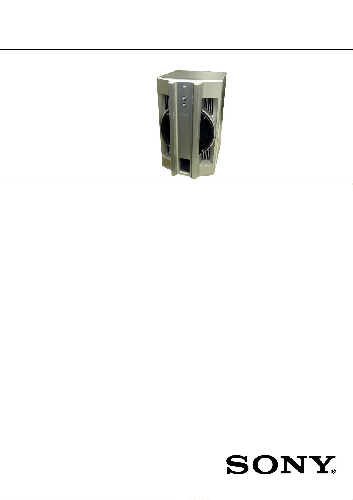
• SA-GN10 is the optional active subwoofer
in MHC-GN90D/GN100D.
SPECIFICATIONS
System
Type Active Subwoofer (magnetically shielded design)
Speaker unit
Subwoofer: 20 cm dia, cone type
Amplifier section
Continuous RMS output: 150 W (1.0%)
Reproduction frequency range
20 Hz – 200 Hz
High frequency cut-off frequency
50 Hz – 200 Hz
E Model
Inputs
Input jacks
LINE IN: input pin jack
General
Power requirements
110 - 120 V or 220 - 240 V, 50/60 Hz
Power consumption
160 W
Dimensions
Approx. 265 x 430 x 400 mm (w/h/d)
Mass 13 kg
Supplied accessories
Foot pads (4)
Audio connecting cord (1 phono – 1 phono), 2 m (1)
Design and specifications are subject to change without notice.
ACTIVE SUBWOOFER
9-877-981-01
2004G0278-1
© 2004.07
Sony Corporation
Home Audio Company
Published by Sony Engineering Corporation

SA-GN10
TABLE OF CONTENTS
Specifications ............................................................................ 1
1. GENERAL
Locating the Controls ...................................................... 3
2. DIAGRAMS
2-1. Printed Wiring Boards – MAIN Section – ............... 4
2-2. Printed Wiring Boards – POWER Section – ............ 5
2-3. Schematic Diagram .................................................. 6
3. EXPLODED VIEWS
3-1. Front Section ............................................................ 7
3-2. Rear Section ............................................................. 8
4. ELECTRICAL PARTS LIST .................................. 9
SAFETY-RELATED COMPONENT WARNING!!
COMPONENTS IDENTIFIED BY MARK 0 OR DOTTED LINE
WITH MARK 0 ON THE SCHEMATIC DIAGRAMS AND IN THE
PARTS LIST ARE CRITICAL TO SAFE OPERATION.
REPLACE THESE COMPONENTS WITH SONY PARTS WHOSE
PART NUMBERS APPEAR AS SHOWN IN THIS MANUAL OR IN
SUPPLEMENTS PUBLISHED BY SONY.
2
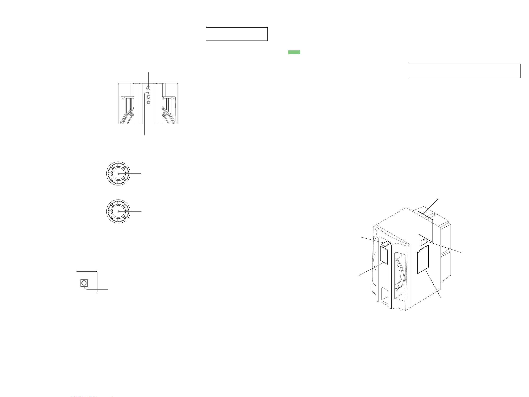
• LOCATING THE CONTROLS
– Front View (a part) –
SECTION 1
GENERAL
SUBWOOFER ON/OFF
Indicator SUBWOOFER ON/OFF
This section is extracted from
instruction manual.
For Printed Wiring Boards:
Note:
• X : parts extracted from the component side.
•
: Pattern from the side which enables seeing.
SECTION 2
DIAGRAMS
For schematic diagrams.
Note:
• All capacitors are in µF unless otherwise noted. (p: pF) 50 WV or
less are not indicated except for electrolytics and tantalums.
• All resistors are in Ω and 1/
• C : panel designation.
Note: The components identified by mark 0 or dotted line with
• A : B+ Line.
• B : B– Line.
•Voltages are dc with respect to ground under no-signal conditions.
no mark : Power on
•Voltages are taken with a VOM (Input impedance 10 MΩ).
Voltage variations may be noted due to normal production
tolerances.
• Signal path.
F : AUDIO
W or less unless otherwise specifed.
4
mark 0 are critical for safety.
Replace only with part number specified.
SA-GN10
– Rear View (a part) –
INPUT
CUT OFF FREQ
50Hz 200Hz
SUBWOOFER LEVEL
MIN MAX
INPUT
CUT OFF FREQ
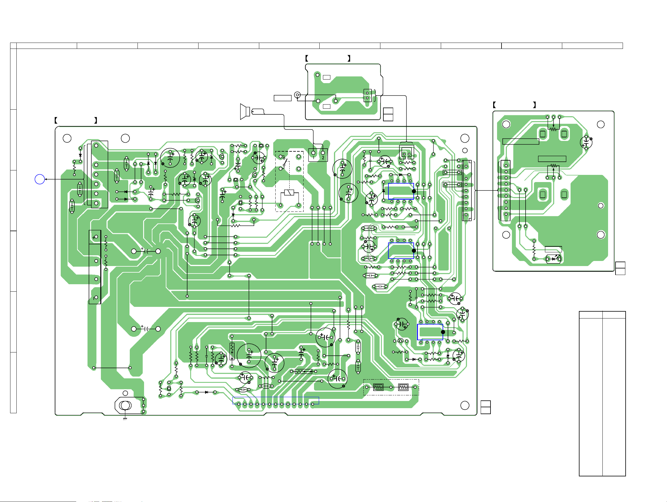
• Circuit Boads Location
MAIN board
SUBWOOFER LEVEL
POWER SWITCH board
INPUT board
PANEL board
POWER TRANS board
SA-GN10
33
SA-GN10
2-1. PRINTED WIRING BOARDS –MAIN Section– • See page 3 for Circuit Boards Location.
1
2
A
MAIN BOARD
3 4 5 6 7
SP1
SPEAKER
J201
INPUT
INPUT BOARD
NO603
1
1-863-682-
11
(11)
8
9 10
PANEL BOARD
RV202
SUBWOOFER LEVEL
CN201
9
JW201
1
JW202
CUT OFF FREQ
R201
RV201
D201
POWER
B
R401
A
POWER
TRANS
C
BOARD
(Page 5)
C804
D401
C803
CN801
1
6
R801
C811
D801
D804
C812
JW151
JW150
C806
C801
D802
D803
C805
R806
JW153
R804
R805
C808
JW152
C810
R803
JW136
D822
JW137
C807
E
C809
C402
Q802
Q801
D821
E
D400
JW141
JW140
JW139
JW138
R402
R403
C401
Q401
JW143
Q402
R400
D
R802
D805
E
JW135
F
C802
R302
Q302
EP801
E
R330
JW134
R333
R303
R304
R300
C322
D303
JW161
R301
C304
C313
C303
1
E
R405
C306
Q404
JW132
Q403
E
R404
R334
C334
E
C403
R406
JW160
JW131
C307
JW129
RY400
IC301
C344
JW126
C310
R306
JW130
BC401
JW147
JW146
R308
13
JW148
JW149
R318
JW125
JW127
C311
C603
JW124
C623
C607
C606
R610
R354
C384
C354
R602
R631
C604
R603
C605
R607
C608
JW123
JW122
R630
R604
JW101
C602
C601
D602
R609
R611
C609
5
R605
R608
4
R312
IC601
4
5
IC602
C612
Q601
R616
R606
JW121
S
1
D601
1
8
R619
D603
CN602
R600
R601
8
1
JW105
JW107
JW108
JW111
JW112
JW113
JW114
C614
5
IC603
4
JW102
JW612
JW621
JW103
JW104
JW109
JW110
JW115
R617
R618
JW162
R615
R614
1-863-685-
JW164
8
1
JW622
C610
JW163
D604
1
9
CN601
C613
JW119
R613
C615
11
(11)
C611
1-863-684-
11
(11)
• Semiconductor
Location
Ref. No.
D201 A-9
D303 F-4
D400 C-4
D401 B-2
D601 C-7
D602 C-6
D603 F-7
D604 F-8
D801 C-2
D802 B-3
D803 B-3
D804 C-2
D805 D-2
D821 B-4
D822 C-3
IC301 F-5
IC601 C-7
Location
IC602 D-7
(CHASSIS)
IC603 E-7
SA-GN10
Q302 F-3
Q401 C-4
Q402 C-4
Q403 B-5
Q404 C-4
Q601 E-7
Q801 B-4
Q802 C-4
4
4
 Loading...