

Page 1
SERVICE MANUAL
MODEL
.............. ......... ....................
DEST. CHASSIS NO. MODEL DEST. CHASSIS NO.
PVM-14L5 US/CND SCC-G61K-A
PVM-20L5 US/CND SCC-G61L-A
PVM-D14L5A AUS SCC-H03D-A
PVM-D20L5A AUS SCC-H03E-A
.............. ......... ....................
REVISED-1
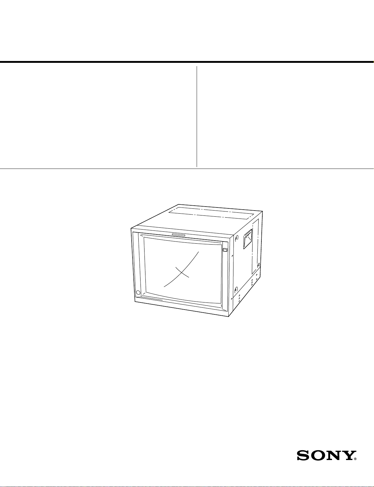
TRINITRON® COLOR VIDEO MONITOR
Page 2

! WARNING
This manual is intended for qualified service personnel only.
To reduce the risk of electric shock, fire or injury, do not perform any servicing other than that
contained in the operating instructions unless you are qualified to do so. Refer all servicing to
qualified service personnel.
! WARNUNG
Die Anleitung ist nur für qualifiziertes Fachpersonal bestimmt.
Alle Wartungsarbeiten dürfen nur von qualifiziertem Fachpersonal ausgeführt werden. Um die
Gefahr eines elektrischen Schlages, Feuergefahr und Verletzungen zu vermeiden, sind bei
Wartungsarbeiten strikt die Angaben in der Anleitung zu befolgen. Andere als die angegeben
Wartungsarbeiten dürfen nur von Personen ausgeführt werden, die eine spezielle Befähigung
dazu besitzen.
! AVERTISSEMENT
Ce manual est destiné uniquement aux personnes compétentes en charge de l’entretien. Afin
de réduire les risques de décharge électrique, d’incendie ou de blessure n’effectuer que les
réparations indiquées dans le mode d’emploi à moins d’être qualifié pour en effectuer d’autres.
Pour toute réparation faire appel à une personne compétente uniquement.
WARNING!!
AN INSULATED TRANSFORMER SHOULD BE USED DURING
ANY SERVICE TO AVOID POSSIBLE SHOCK HAZARD, BECAUSE OF LIVE CHASSIS.
THE CHASSIS OF THIS RECEIVER IS DIRECTLY CONNECTED
TO THE AC POWER LINE.
SAFETY-RELATED COMPONENT WARNING !!
COMPONENTS IDENTIFIED BY A
DIAGRAMS, EXPLODED VIEWS AND IN THE PARTS LIST ARE
CRITICAL TO SAFE OPERATION. REPLACE THESE COMPONENTS WITH SONY PARTS WHOSE P ART NUMBERS APPEAR
AS SHOWN IN THIS MANUAL OR IN SUPPLEMENTS PUBLISHED BY SONY . CIRCUIT ADJUSTMENTS THAT ARE CRITICAL TO SAFE OPERATION ARE IDENTIFIED IN THIS MANU AL.
FOLLOW THESE PROCEDURES WHENEVER CRITICAL COMPONENTS ARE REPLACED OR IMPROPER OPERATION IS
SUSPECTED.
!!
! MARK ON THE SCHEMA TIC
!!
ATTENTION!!
AFIN D’ÉVITER TOUT RISQUE D’ÉLECTROCUTION
PROVENANT D’UN CHÂSSIS SOUS TENSION, UN
TRANSFORMA TEUR D’ISOLEMENT DOIT ETRE UTILISÉ LORS
DE TOUT DÉPANNAGE.
LE CHÂSSIS DE CE RÉCEPTEUR EST DIRECTEMENT
RACCORDÉ Á L’ALIMENTATION SECTEUR.
ATTENTION AUX COMPOSANTS RELATIFS Á LA
SÉCURITÉ!!
LES COMPOSANTS IDENTIFIÉS PAR UNE MAPQUE
LES SCHÉMAS DE PRINCIPE, LES VUES EXPLOSÉES ET LES
LISTES DE PIECES SONT D’UNE IMPORTANCE CRITIQUE
POUR LA SÉCURITÉ DU FONCTIONNEMENT. NE LES
REMPLACER QUE PAR DES COMPOSANTS SONY DONT LE
NUMÉRO DE PIÈCE EST INDIQUÉ DANS LE PRÉSENT
MANUEL OU DANS DES SUPPLÉMENTS PUBLIÉS P AR SONY.
LES RÉGLAGES DE CIRCUIT DONT L’IMPORTANCE EST CRITIQUE POUR LA SÉCURITÉ DU FONCTIONNEMENT SONT
IDENTIFIÉS DANS LE PRÉSENT MANUEL. SUIVRE CES
PROCÉDURES LORS DE CHAQUE REMPLACEMENT DE
COMPOSANTS CRITIQUES, OU LORSQU’UN MAUVAIS
FONCTIONNEMENT EST SUSPECTÉ.
PVM-14L5/20L5/D14L5A/D20L5A
!!
! SUR
!!
Page 3

Table of Contents
1. Service Informations
1-1. Board Layout (14 inch) ...............................................................................1-1
1-2. Disassembly (14 inch).................................................................................1-1
1-2-1. Top Cover Removal (14 inch)....................................................1-1
1-2-2. Bezel Assy Removal (14 inch)...................................................1-2
1-2-3. H1 Board Removal (14 inch) .....................................................1-2
1-2-4. H2 Board Removal (14 inch) .....................................................1-3
1-2-5. J , D1, D2 and D Boards Removal (14 inch) .............................1-3
1-2-6. C Board Removal (14 inch) .......................................................1-4
1-2-7. B Block Assy Removal (14 inch)...............................................1-4
1-2-8. K, T, B1, M and B Boards Removal (14 inch) ..........................1-5
1-2-9. Q Block Assy Removal (14 inch) ..............................................1-5
1-2-10. Removal of Anode Cap .............................................................. 1-6
1-2-11. G Board Removal (14 inch) .......................................................1-6
1-2-12. Picture Tube Removal (14 inch) ................................................1-7
1-2-13. Speaker Removal (14 inch) ........................................................ 1-8
1-2-14. Service Position (14 inch) ..........................................................1-8
1-3. Board Layout (20 inch) ...............................................................................1-9
1-4. Disassembly (20 inch)...............................................................................1-10
1-4-1. Top Cover Removal (20 inch)..................................................1-10
1-4-2. Bezel Assy Removal (20 inch).................................................1-10
1-4-3. HA Board Removal (20 inch) .................................................. 1-11
1-4-4. HB Board Removal (20 inch) ..................................................1-11
1-4-5. J, D1, D2 and D Boards Removal (20 inch) ............................1-12
1-4-6. C Board Removal (20 inch) .....................................................1-12
1-4-8. K, T, B1, M and B Boards Removal (20 inch) ........................1-13
1-4-7. B Block Removal (20 inch)......................................................1-13
1-4-9. Q Block Assy Removal (20 inch) ............................................1-14
1-4-10. Removal of Anode Cap ............................................................ 1-14
1-4-11. G Board Removal (20 inch) .....................................................1-15
1-4-12. Picture Tube Removal (20 inch) ..............................................1-15
1-4-13. Speaker Removal (20 inch) ...................................................... 1-16
1-4-14. Service Position (20 inch) ........................................................1-16
2. Set-up Adjustment
2-1. Equipment Required....................................................................................2-1
2-2. Preparations (1) ...........................................................................................2-1
2-3. Preparation (2). Initialization ...................................................................2-16
2-4. Writing Model Data .................................................................................. 2-17
2-5. Picture Output ........................................................................................... 2-17
2-6. Free-run Frequency Adjustment ...............................................................2-17
PVM-14L5/20L5/D14L5A/D20L5A
1
Page 4

2-7. Landing Adjustment..................................................................................2-18
2-8. H Blanking Adjustment.............................................................................2-19
2-9. Linearity Adjustment ................................................................................2-20
2-10. Convergence Adjustment (1) .................................................................... 2-21
2-11. Deflection Yoke Neck Rotation Adjustment ............................................ 2-22
2-12. Convergence Adjustment (2) .................................................................... 2-22
2-13. G2 Adjustment ..........................................................................................2-23
2-14. White Balance Adjustment (15k)..............................................................2-23
2-15. White Balance Adjustment (33k)..............................................................2-24
2-16. SUB BRIGHT, SUB CONTRAST Adjustment (15 K) ............................ 2-24
2-17. SUB BRIGHT, SUB CONTRAST Adjustment (33 K) ............................ 2-25
2-18. White Balance Interference Correction Adjustment ................................. 2-25
2-18-1. NTSC Composite Adjustment..................................................2-25
2-18-2. PAL Composite Adjustment .................................................... 2-25
2-18-3. COMPONENT Adjustment ..................................................... 2-25
2-18-4. SDI Adjustment........................................................................2-25
2-18-5. HD and SDI Adjustments.........................................................2-26
2-19. Focus Adjustment......................................................................................2-26
3. Safety Related Adjustment
3-1. High Tension Regulator Confirmation........................................................3-2
3-2. Protection Circuit Confirmation..................................................................3-2
3-2-1. HV Protector Circuit Confirmation............................................3-2
3-2-2. 1K Protector Circuit Confirmation.............................................3-2
4. Electrical Adjustments
4-1. Equipment Required....................................................................................4-1
4-2. B Board Adjustments ..................................................................................4-2
4-2-1. Preparations ................................................................................ 4-2
4-2-2. 15k YPBPR SMPTE (601) Signal Adjustment..........................4-3
4.2-2-1. Black Level Adjustment.............................................................4-3
4-2-2-2. CHROMA Leak Adjustment......................................................4-4
4-2-2-3. MATRIX Adjustment ................................................................ 4-4
4-2-3. 15k YPBPR BETACAM SETUP 0 Signal Adjustment ............4-5
4-2-4. 15k YPBPR BETACAM SETUP 7.5 Signal Adjustment .........4-5
4-2-5. 33 k YPBPR SMPTE (709) Signal Adjustment.........................4-6
4-3. B1 Board Adjustments ................................................................................4-8
4-3-1. Preparation .................................................................................4-8
4-3-2. Y OUT Level Adjustment (BYPASS Mode) ............................. 4-9
4-3-3. Clamp Pulse Width Adjustment (NTSC) ...................................4-9
4-3-4. Burst Gate Pulse Width Adjustment (NTSC) ............................4-9
2
PVM-14L5/20L5/D14L5A/D20L5A
Page 5

4-3-5. 3.58 f0 Adjustment (NTSC) ....................................................... 4-9
4-3-6. Phase Adjustment (NTSC) .........................................................4-9
4-3-7. Level Adjustment (NTSC) .......................................................4-10
4-3-8. Burst Gate Pulse Width Adjustment (PAL) .............................4-10
4-3-9. 4.43 f0 Adjustment (PAL)........................................................4-10
4-3-10. PAL B-Y PHASE Adjustment .................................................4-10
4-3-11. PAL PHASE Adjustment (Normal) .........................................4-11
4-3-12. Level Adjustment (PAL)..........................................................4-11
4-3-13. Level Adjustment (NTSC 443) ................................................4-11
4-3-14. Clamp Pulse Width Adjustment (SECAM) ............................. 4-12
4-3-15. H. Pulse Width Adjustment (SECAM) ....................................4-12
4-3-16. Level Adjustment (SECAM)....................................................4-12
5. Theory of Operation
5-1. B Board ....................................................................................................... 5-1
5-2. BI Board ......................................................................................................5-3
5-3. C Board ....................................................................................................... 5-4
5-4. Deflection Circuit and High Tension Circuit ..............................................5-5
5-7. Power Supply Circuit ..................................................................................5-7
6. Semiconductors................................................................................. 6-1
7. Spare Parts
7-1. Notes on Repair Parts..................................................................................7-1
7-2. Exploded Views ..........................................................................................7-2
7-3. Electrical Parts List ...................................................................................7-11
8. Block Diagrams
Overall (1/2) ................................................................................................8-1
Overall (2/2) ................................................................................................8-2
Q (1/2), B (1/5), T (1/2), K..........................................................................8-3
B (2/5) ......................................................................................................... 8-4
B (3/5) ......................................................................................................... 8-5
Q (2/2), B (4/5, 5/5), M, T (2/2), H1 (14L)/HA (20L), H2 (14L)/HB (20L) ...
B1 ................................................................................................................8-7
C, D, D1, D2, DY........................................................................................8-8
G, J .............................................................................................................. 8-9
8-6
PVM-14L5/20L5/D14L5A/D20L5A
3
Page 6

9. Diagrams
9-1. Frame Schematic Diagram .......................................................................... 9-3
Frame...........................................................................................................9-3
9-2. Schematic Diagrams and Printed Wiring Boards........................................9-4
Schematic Diagrams
Q (1/2) .........................................................................................................9-5
Q (2/2) .........................................................................................................9-6
T .................................................................................................................. 9-8
B (1/5) ....................................................................................................... 9-11
B (2/5) ....................................................................................................... 9-12
B (3/5) ....................................................................................................... 9-13
B (4/5) ....................................................................................................... 9-14
B (5/5) ....................................................................................................... 9-15
B1 (1/2) .....................................................................................................9-21
B1 (2/2) .....................................................................................................9-22
M ............................................................................................................... 9-24
H1 .............................................................................................................. 9-25
H2 .............................................................................................................. 9-27
HA .............................................................................................................9-29
HB .............................................................................................................9-30
K ................................................................................................................ 9-31
C ................................................................................................................9-33
X ................................................................................................................ 9-34
J ................................................................................................................. 9-35
D ................................................................................................................ 9-37
D2 .............................................................................................................. 9-37
D1 .............................................................................................................. 9-39
G (1/2) .......................................................................................................9-42
G (2/2) .......................................................................................................9-43
Printed Wiring Boards
Q .................................................................................................................. 9-4
T .................................................................................................................. 9-7
B ................................................................................................................9-16
B1 ..............................................................................................................9-20
M ............................................................................................................... 9-23
H1 .............................................................................................................. 9-23
H2 .............................................................................................................. 9-26
HA .............................................................................................................9-28
HB .............................................................................................................9-28
K ................................................................................................................ 9-31
C ................................................................................................................9-32
X ................................................................................................................ 9-34
J ................................................................................................................. 9-35
D2 .............................................................................................................. 9-35
D ................................................................................................................ 9-36
D1 .............................................................................................................. 9-38
G ................................................................................................................ 9-40
4
PVM-14L5/20L5/D14L5A/D20L5A
Page 7
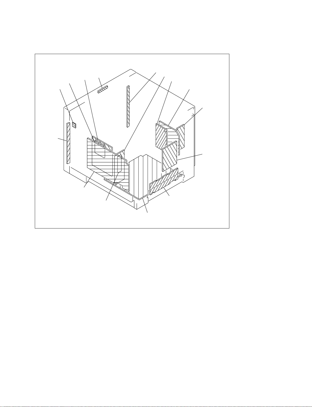
1-1. Board Layout (14 inch)
Section 1
Service Informations
X
B1
M
J
H1
B
K
G
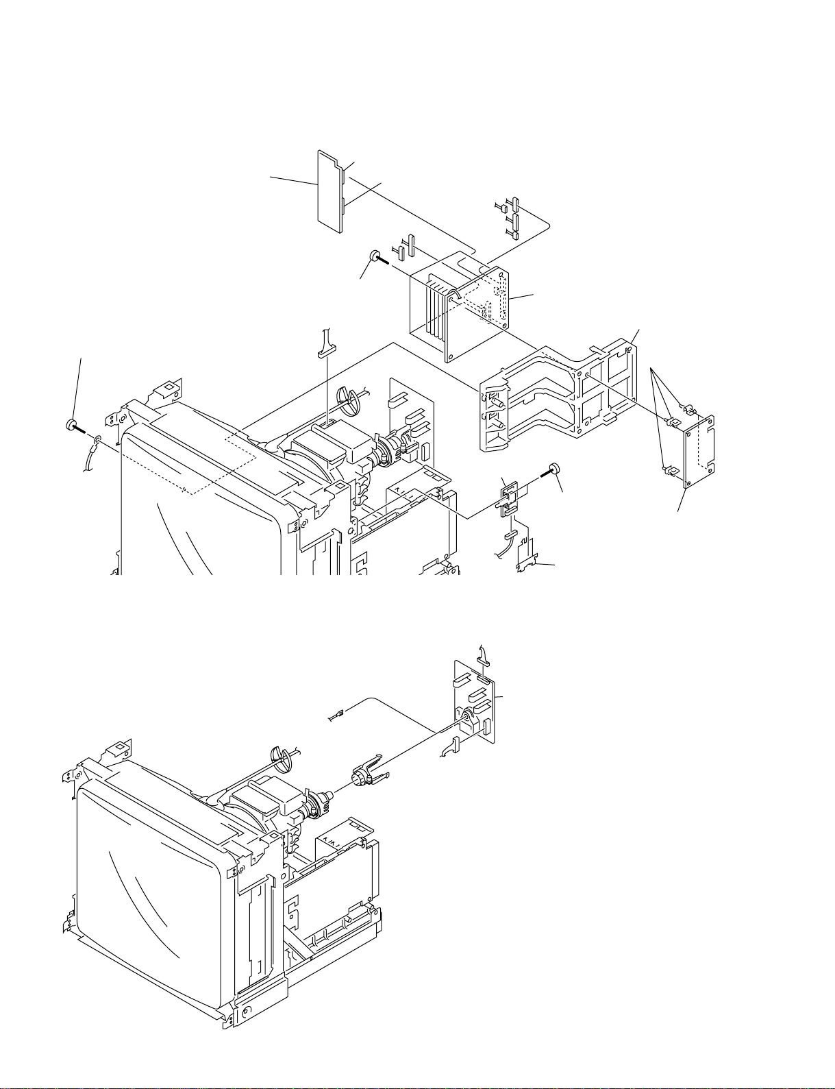
1-2. Disassembly (14 inch)
H2
T
D2
D
Q
D1
C
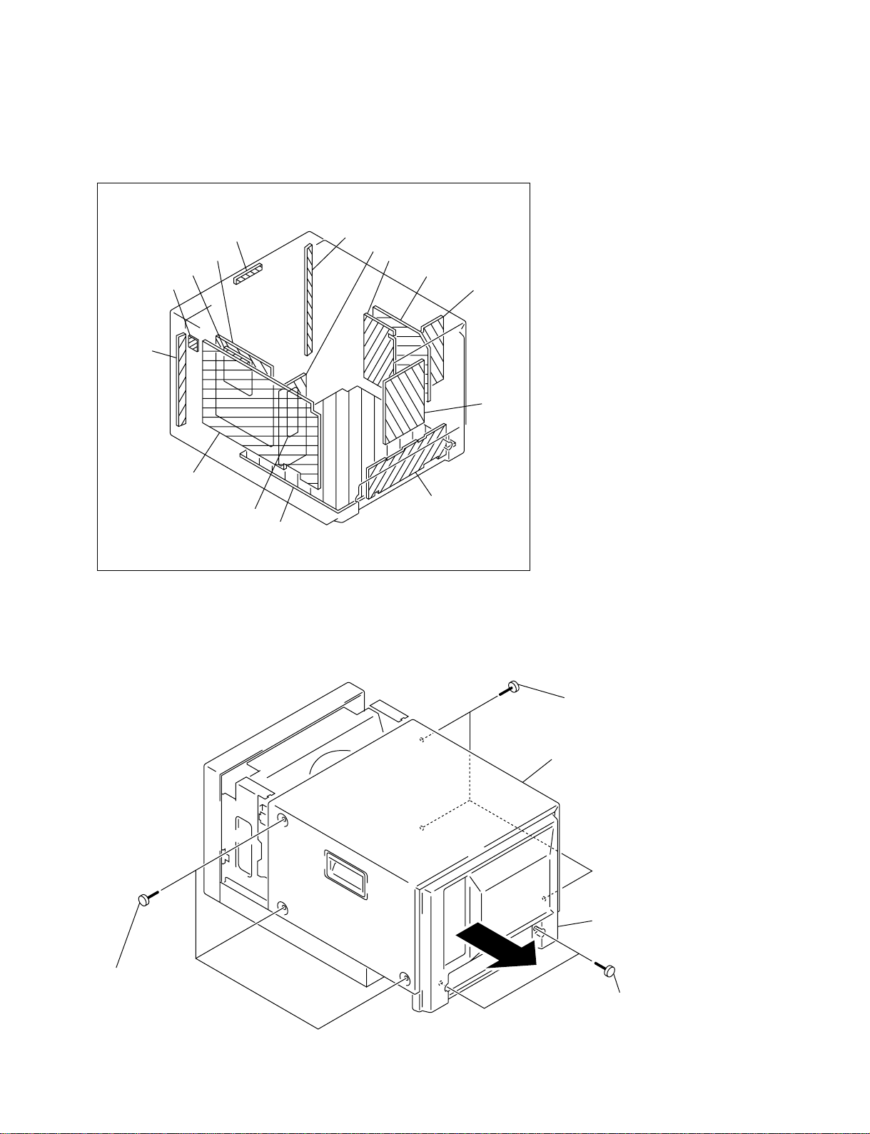
1-2-1. Top Cover Removal (14 inch)
1 Three screws
(claw case screw (OS))
4
2 Three screws
(claw case screw (OS))
Top cover
Rear cover
3 T wo screws
(+BVTT 4 x 8)
PVM-14L5/20L5/D14L5A/D20L5A
1-1
Page 8
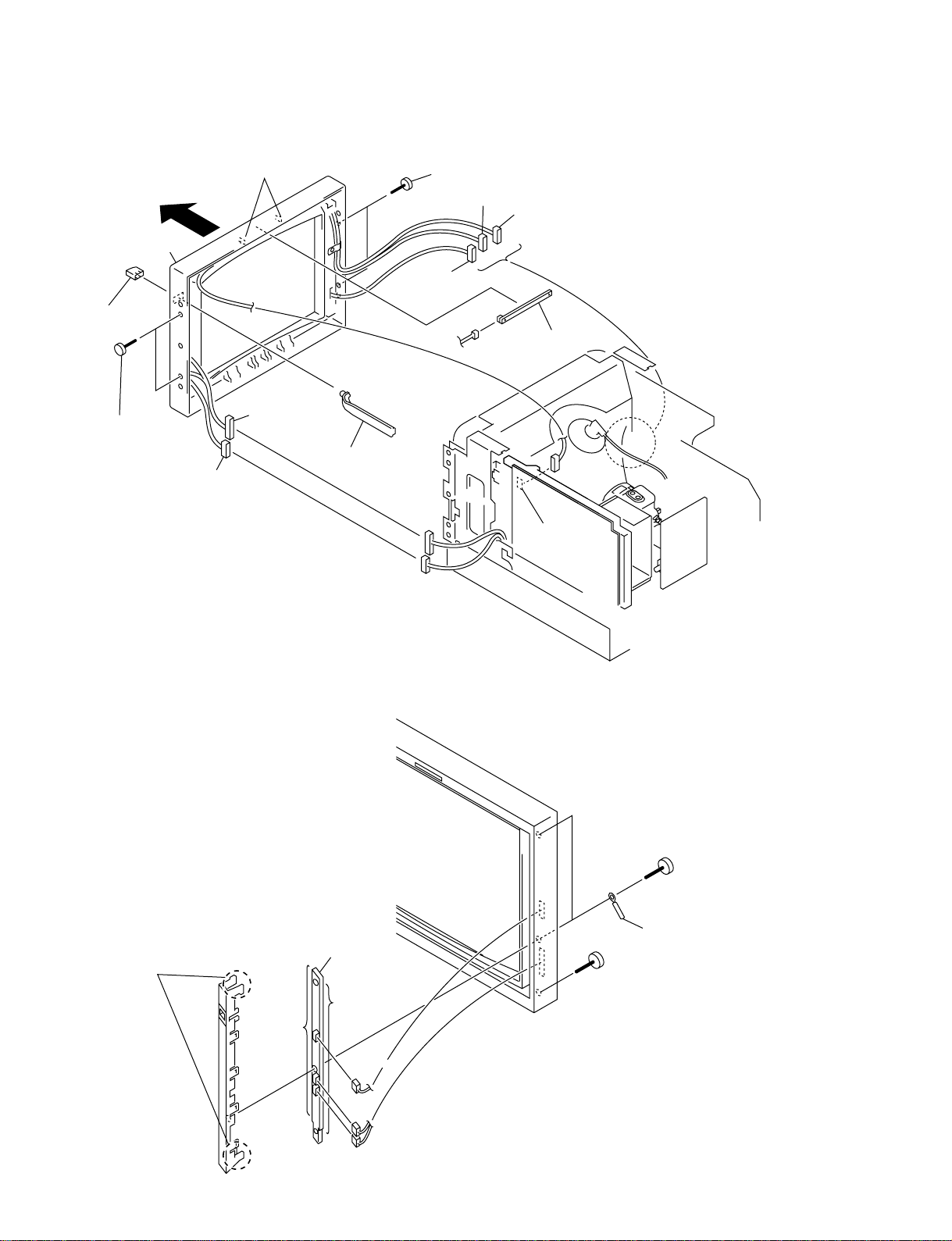
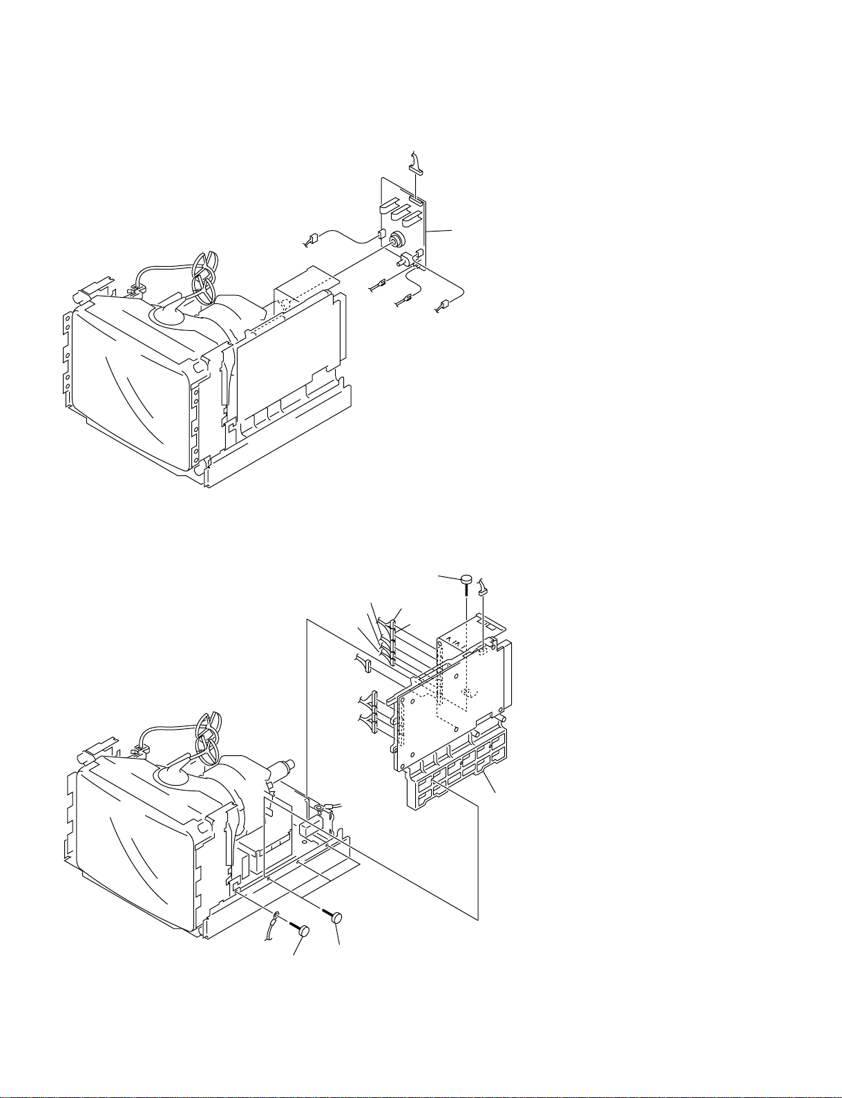
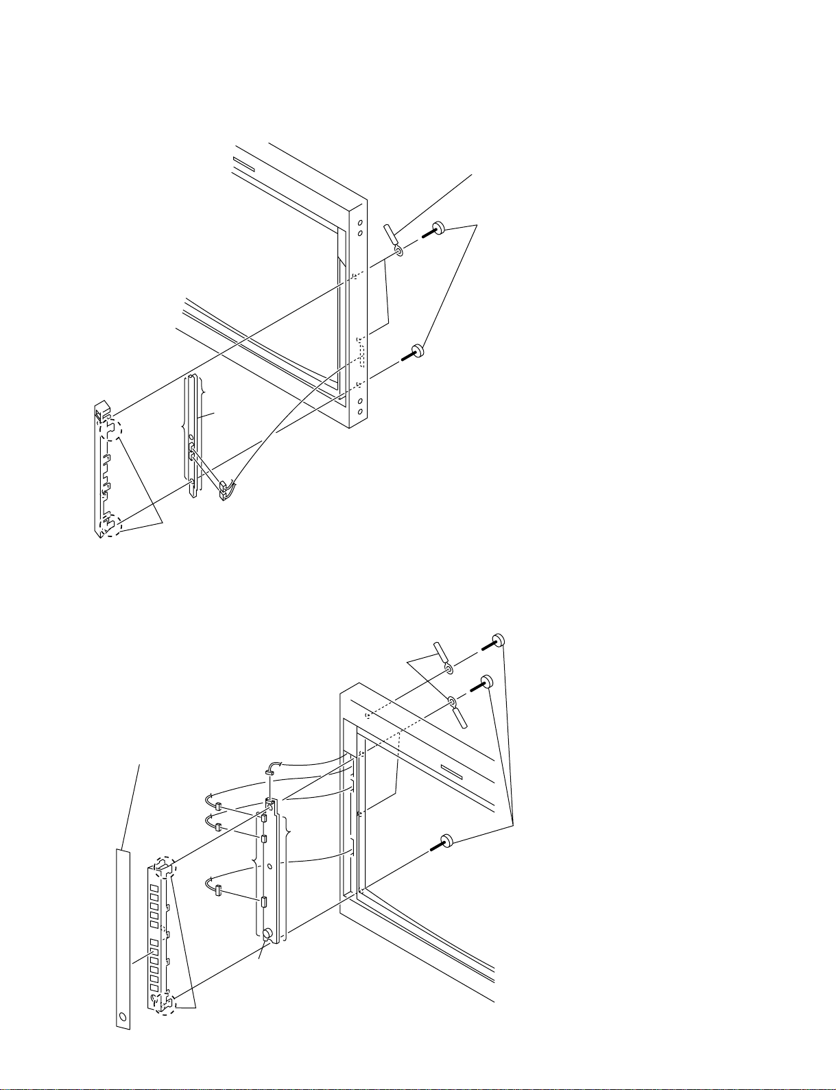
1-2-2. Bezel Assy Removal (14 inch)
Bezel assy
1 Power button
2 Two screws
(+B 3 x 8)
4
5 pin
6 Two claws
10 pin
5 Shaft switch
3 Two screws (+B 3 x 8)
7 pin
9 pin
9 pin
X board
CN900
CN105
1-2-3. H1 Board Removal (14 inch)
H1 board
4 Four claws
5 Three
claws
6 Four claws
CN2903
1 Two screws
(+BVTP 3 x 12)
2 Two wire holders
3 Screw (+BVTP 3 x 12)
CN2902
1-2
CN2901
PVM-14L5/20L5/D14L5A/D20L5A
Page 9
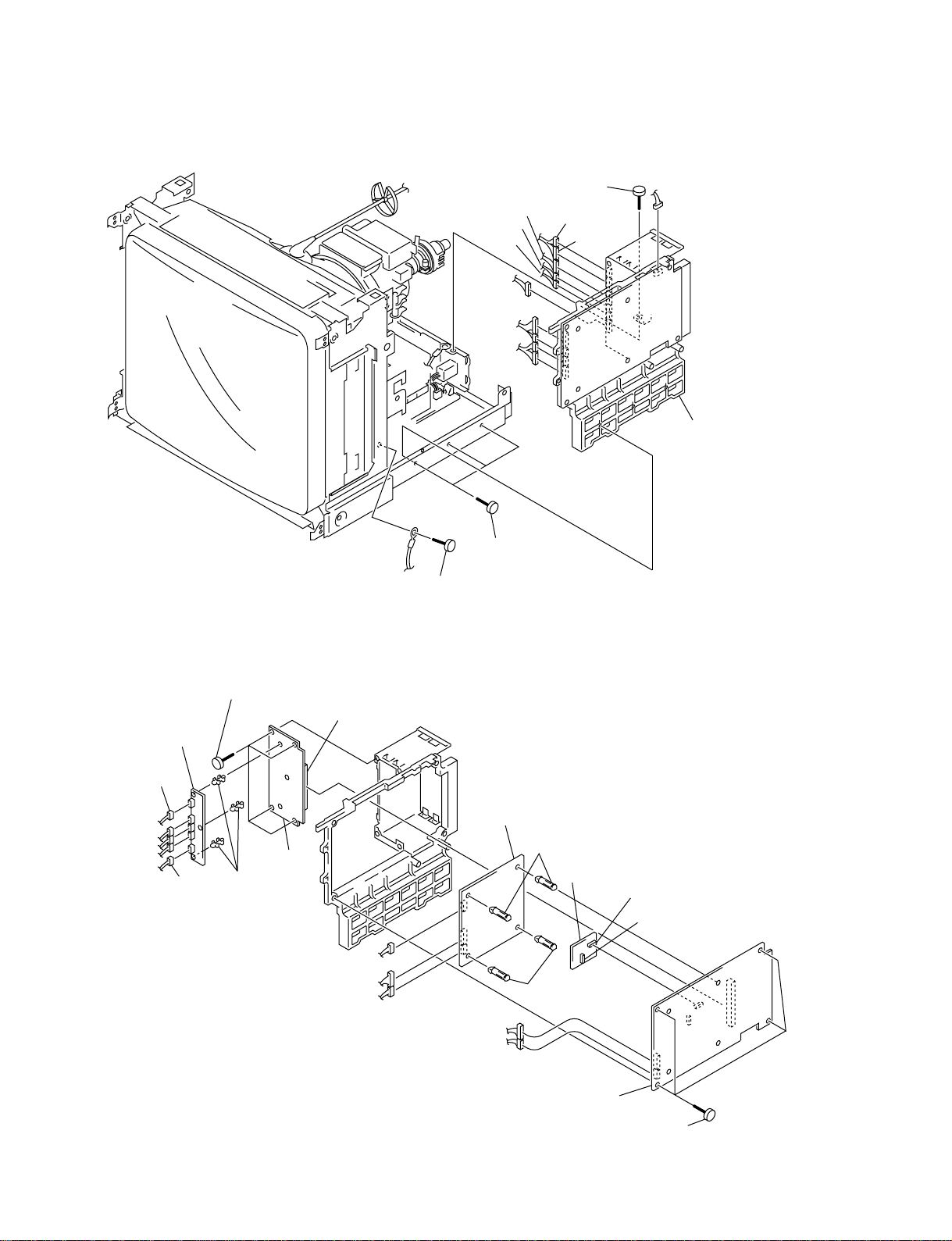
1-2-4. H2 Board Removal (14 inch)
1 Screw (+BVTP 3 x 12)
CN5005
CN5002
CN5001
4 Four claws
CN5004
3 Four claws
H2 board
5 Four
claws
1-2-5. J , D1, D2 and D Boards Removal (14 inch)
CN2502 (board to board)
CN2501 (board to board)
4 D1 board
CN1506
CN1507
CN1508
2 Wire holder
CN1501
CN1502
CN1503
5 Screw (+BVTT 4 x 8)
PVM-14L5/20L5/D14L5A/D20L5A
6 Four screws
(+BVTP 3 x 12)
CN706
CN951
D board
9 Bracket D
7 Four card edge
spacers
1 Two screws
(+PSW 3 x 8)
3 J board
8 D2 board
2 Insulator (J PWB)
1-3
Page 10
1-2-6. C Board Removal (14 inch)
CN701
CN702
1-2-7. B Block Assy Removal (14 inch)
3 Screw (+PSW 4 x 8)
CN1903
CN1907
CN703
CN1904
CN705
CN1908
CN1905
C board
CN704
CN2401
CN1906
CN102
1 Screw (+BVTP 3 x 8)
CN101
CN103
CN104
B block assy
2 Three screws (+BVTP 3 x 12)
1-4
PVM-14L5/20L5/D14L5A/D20L5A
Page 11
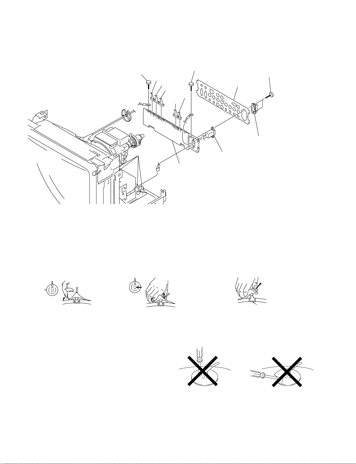
1-2-8. K, T, B1, M and B Boards Removal (14 inch)
9 Four screws (+BVTT 3 x 8)
CN1901 (board to board)
2 K board
CN3504
CN3505
CN3503
CN3502
CN3501
T board
1 Three PWB
holders
CN801
CN3802
CN3801
1-2-9. Q Block Assy Removal (14 inch)
1 Screw (+PSW 4 x 8)
CN113
CN201
CN2706
CN2707
CN2710
CN2705
5 B1 board
3 Two PWB holders
6 M board
CN107 (board to board)
CN108 (board to board)
4 Two PWB
holders
8 B board
7 Four screws
(+BVTP 3 x 12)
3 Screw (+PSW 4 x 8)
4 Two screws
(+PSW 3 x 12)
6 Connector label
CN2704
PVM-14L5/20L5/D14L5A/D20L5A
2 Four claws
CN601
5 Plug holder (A)
7 AC inlet 3p (with noise filter)
8 Q block assy
1-5
Page 12
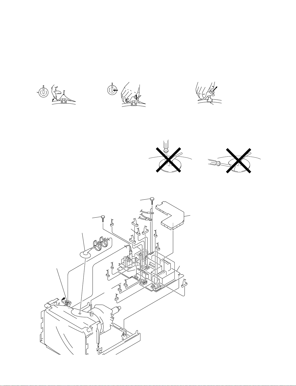
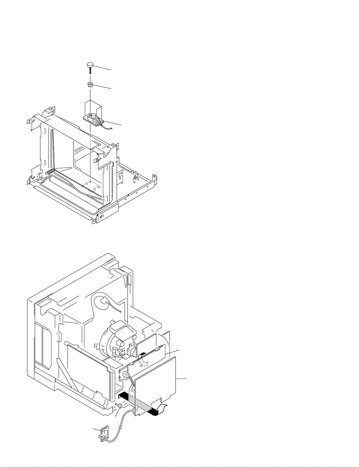
1-2-10.Removal of Anode Cap
c
Anode button
n
Short-circuit the anode of the picture tube and the anode cap to the metal chassis, picture tube shield or carbon painted on
the picture tube, after removing the anode.
..
. Removal Procedure
..
b
a
a
b
(1) Turn up one side of the rubber cap in the
direction indicated by arrow a.
(2) Using a thumb, pull up the rubber cap
firmly in the direction indicated by
arrow b.
..
. Handling Precautions
..
(1) Do not scratch the surface of anode cap with a sharp object.
(2) Do not press the rubber so hard that it damages the inside of
anode caps. A shatter-hook terminal is built into the rubber.
(3) Do not turn the foot of the rubber over.
The shatter-hook terminal will stick out or damage the rubber.
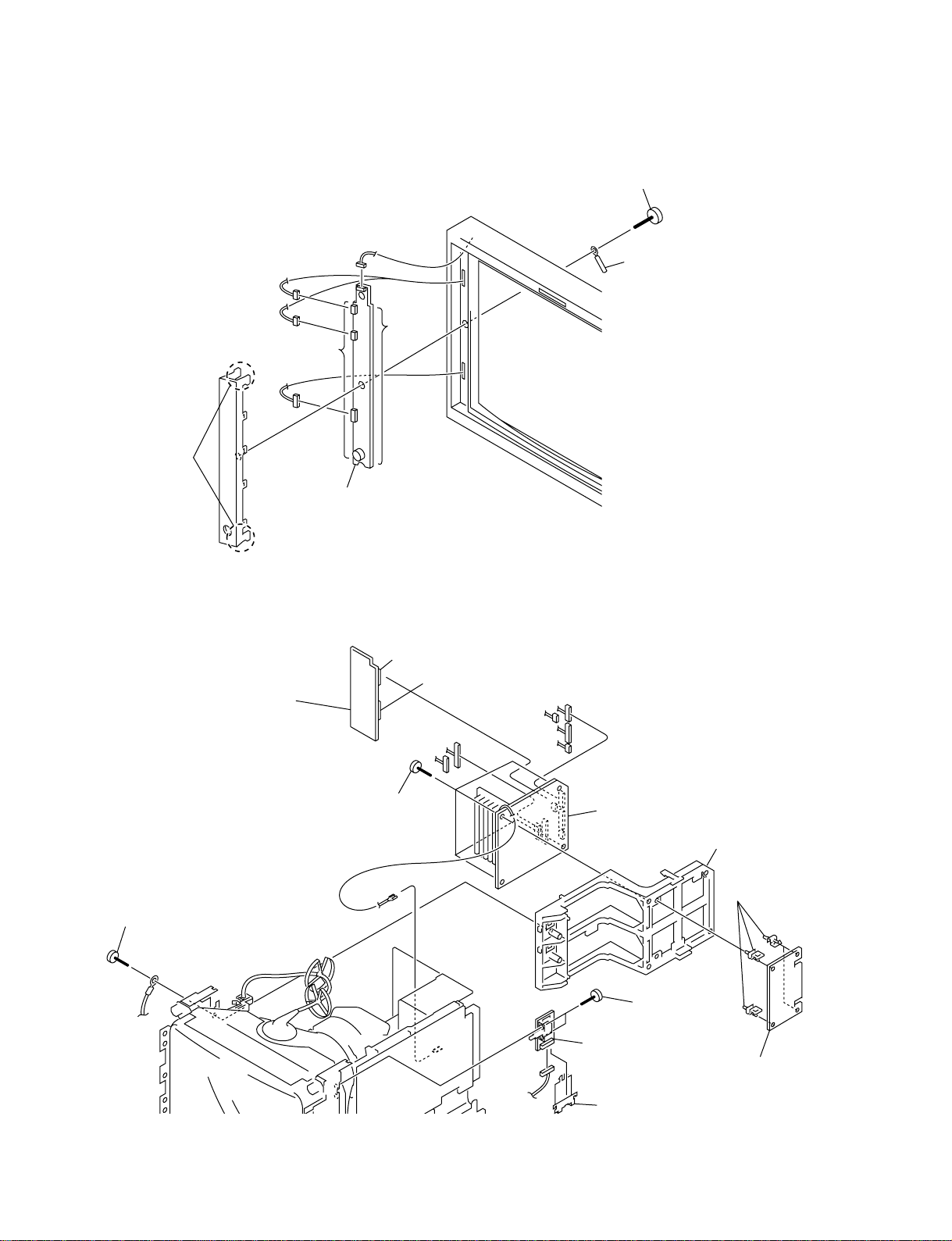
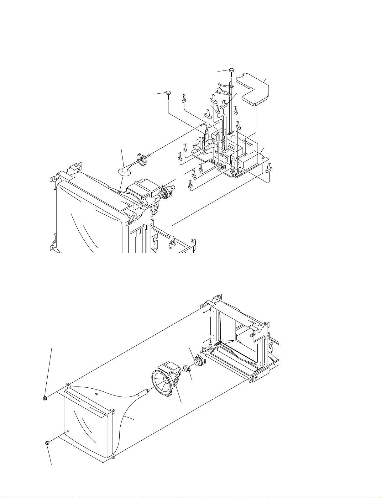
1-2-11.G Board Removal (14 inch)
4 Two screws (+PSW 4 x 8)
3
Screw (+BVTP 3 x 16)
1 Anode cap
CN505
CN607
CN606
CN503
(3) When one side of the rubber cap is
separated from the anode button, the
anode-cap can be removed by turning
up the rubber cap and pulling up it in
the direction of the arrow c.
6 G shield
CN608
CN608
CN607
2 Open the lead holder in the
direction of the arrow.
1-6
CN604
CN508
CN603
CN609
CN610
5 G board
CN602
PVM-14L5/20L5/D14L5A/D20L5A
Page 13
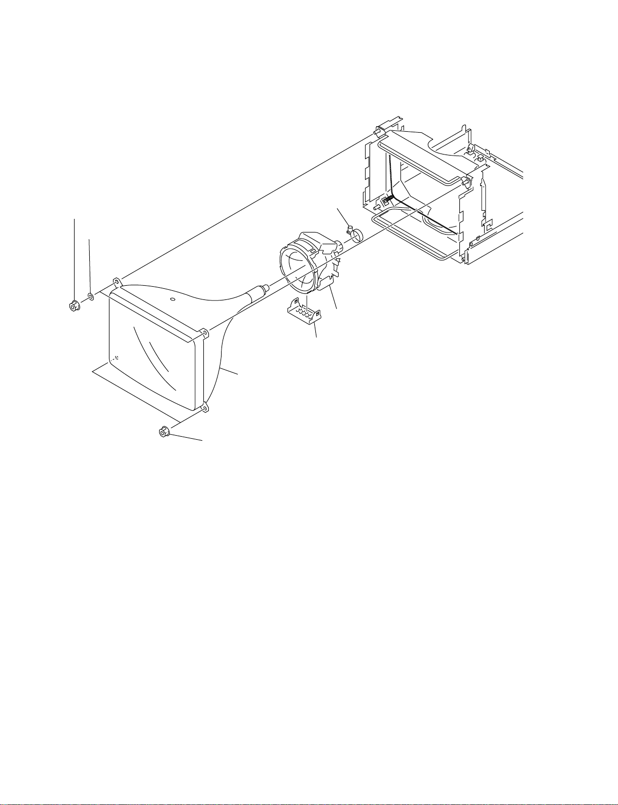
1-2-12. Picture Tube Removal (14 inch)
4 Two nuts (flange nut (B) M5)
5 Two washers
(CRT position washer)
1 Fastening band assy
3 Deflection yoke
2 DY shield
7 Picture tube
6 Two nuts (flange nut (B) M5)
PVM-14L5/20L5/D14L5A/D20L5A
1-7
Page 14
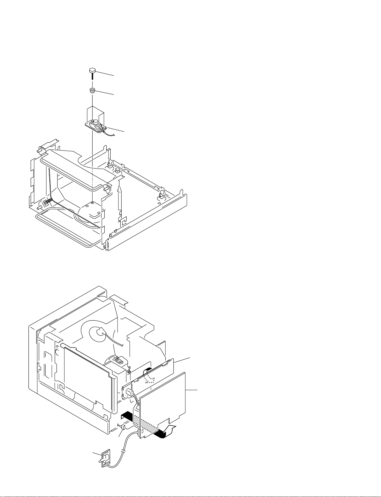
1-2-13.Speaker Removal (14 inch)
1 Four screws (step screw M3 x 4)
2 Four speaker cushions
3 Speaker
1-2-14.Service Position (14 inch)
CN603
J board
*Because there exist the portions that have the high tension voltage,
be careful that the printed boards must not touch each other
nor must not touch with the chassis.
Q board
G board
1-8
PVM-14L5/20L5/D14L5A/D20L5A
Page 15
1-3. Board Layout (20 inch)
X
M
J
HA
B1
B
HB
T
D2
D
D1
C
K
G
Q
PVM-14L5/20L5/D14L5A/D20L5A
1-9
Page 16
1-4. Disassembly (20 inch)
1-4-1. Top Cover Removal (20 inch)
1 Three screws
(claw case screw (OS))
2 Three screws
(claw case screw (OS))
Top cover
4
1-4-2. Bezel Assy Removal (20 inch)
6 Two claws
4
Bezel assy
1 Power button
2 Two screws
(+B 3 x 8)
5 Shaft switch
Rear cover
3 Two screws (+B 3 x 8)
X board
CN900
10 pin
5 pin
3 Four screws
(+BVTT 4 x 8)
10 pin
9 pin
7 pin
1-10
CN105
PVM-14L5/20L5/D14L5A/D20L5A
Page 17
1-4-3. HA Board Removal (20 inch)
5 Four claws
HA board
4 Three
claws
CN2902
CN2901
3 Four claws
2 Two wire holders
1 Three screws
(+BVTP 3 x 12)
1-4-4. HB Board Removal (20 inch)
2 Three wire holders
3 Control label (L)
CN5002
CN5001
5 Four
claws
CN5004
CN5005
6 Four
claws
HB board
1 Four screws
(+BVTP 3 x 12)
4 Four claws
PVM-14L5/20L5/D14L5A/D20L5A
1-11
Page 18
1-4-5. J, D1, D2 and D Boards Removal (20 inch)
CN2502 (board to board)
4 D1 board
CN2501 (board to board)
CN1506
CN1507
CN1508
CN1502
CN1503
CN1501
6 Four screws
(+BVTP 3 x 12)
5 Screw
(+BVTT 4 x 8)
9 pin
1-4-6. C Board Removal (20 inch)
3 J board
CN951
CN701
D board
1 Two screws
(+PSW 3 x 8)
2 Insulator (J PWB)
9 Bracket D
7 Four card edge
spacers
8 D2 board
1-12
CN704
C board
CN702
PVM-14L5/20L5/D14L5A/D20L5A
Page 19
1-4-7. B Block Assy Removal (20 inch)
3 Screw (+PSW 4 x 8)
CN1904
CN1903
CN1907
CN1906
CN101
CN102
CN103
CN104
2 Three screws
(+BVTP 3 x 12)
1 Screw (+BVTT 4 x 8)
1-4-8. K, T, B1, M and B Boards Removal (20 inch)
CN1908
CN1905
CN2401
B block assy
CN3504
CN3505
CN3503
CN3502
9 Four screws (+BVTT 3 x 8)
2 K board
CN3501
T board
1 Three PWB
holders
CN1901 (board to board)
CN801
CN3802
CN3801
5 B1 board
3 Two PWB holders
6 M board
CN107 (board to board)
CN108 (board to board)
4 Two PWB
holders
CN113
CN201
8 B board
7 Four screws
(+BVTP 3 x 12)
PVM-14L5/20L5/D14L5A/D20L5A
1-13
Page 20
c
Anode button
1-4-9. Q Block Assy Removal (20 inch)
1 Screw (+PSW 4 x 8)
1-4-10.Removal of Anode Cap
CN2706
2 Four claws
CN2707
CN2710
CN2705
CN601
3 Screw (+PSW 4 x 8)
CN2704
8 Q block assy
4 Two screws
(+PSW 3 x 12)
6 Connector label
5 Plug holder (A)
7 AC inlet 3p (with noise filter)
n
Short-circuit the anode of the picture tube and the anode cap to the metal chassis, picture tube shield or carbon painted on
the picture tube, after removing the anode.
..
. Removal Procedure
..
a
a
(1) Turn up one side of the rubber cap in the
direction indicated by arrow a.
..
. Handling Precautions
..
(1) Do not scratch the surface of anode cap with a sharp object.
(2) Do not press the rubber so hard that it damages the inside of
anode caps. A shatter-hook terminal is built into the rubber.
(3) Do not turn the foot of the rubber over.
The shatter-hook terminal will stick out or damage the rubber.
b
b
(2) Using a thumb, pull up the rubber cap
firmly in the direction indicated by
arrow b.
(3) When one side of the rubber cap is
separated from the anode button, the
anode-cap can be removed by turning
up the rubber cap and pulling up it in
the direction of the arrow c.
1-14
PVM-14L5/20L5/D14L5A/D20L5A
Page 21
1-4-11.G Board Removal (20 inch)
2 Screw (+BVTP 3 x 16)
1 Anode cap
3 Two screws (+PSW 4 x 8)
CN505
CN607
CN606
CN503
CN604
CN508
CN609
CN610
CN603
5 G shield
CN608
CN608
CN607
4 G board
CN602
1-4-12.Picture Tube Removal (20 inch)
4 Two nuts (flange nut (B) M5)
6 Picture tube
2 Neck assy
3 Deflection yoke
1 Fastening band
assy
5 Two nuts (flange nut (B) M5)
PVM-14L5/20L5/D14L5A/D20L5A
1-15
Page 22
1-4-13.Speaker Removal (20 inch)
1 Four screws (step screw M3 x 4)
2 Four speaker cushions
3 Speaker
1-4-14.Service Position (20 inch)
*Because there exist the portions that have the high tension voltage,
be careful that the printed boards must not touch each other
nor must not touch with the chassis.
Q board
G board
1-16
CN603
J board
PVM-14L5/20L5/D14L5A/D20L5A
Page 23

Section 2
Set-up Adjustment
2-1. Equipment Required
. Oscilloscope
Sony Tektronix 2465 or equivalent (with bandwidth of
350 MHz)
. NTSC/PAL/SECAM component signal generator
Sony Tektronix TG2000 +AVG1 (option module)
+AWVG2 (option module) or equivalent
. SDI signal generator
Sony Tektronix TSG-422
. Monoscope signal generator
ShibaSoku TP22AX or equivalent
. VG (programmable video signal generator)
. VG814 or equivalent
. Frequency counter
Advantest TR5821AK or equivalent
. Digital VOM
Advantest TR6845 or equivalent
. Slide induction transformer
. High tension voltmeter
. DC power supply
. Ammeter
. Luminance meter
Minolta CA-110 or equivalent.
If the Minolta CA-110 is not available, perform the
measurement by visual inspection by comparing the
monitor that has already been adjusted earlier with the
monitor that you want to adjust.
n
Start the following adjustments after 5 minutes have
passed after the main power is turned on.
* In this chapter, [||||||] indicates the control items in the
service mode.
Example : [60|H-FREQ]
2-2. Preparations (1)
Service Mode
This set is provided with a switch for service on the front
panel that can be used to make various adjustments. The
operation method of this switch is explained in detail below.
1. Entering the service mode
Simultaneously press the [ENTER] key and the
[DEGAUSS] key shown on the display of the menu.
SIGNAL
SIG
• LEVEL-1...
DEF
• LEVEL-2...
OPT
• WHITE BALANCE...
REM
• DECODER COLOR...
SYS
• DECODER LEVEL...
STA
• DETECTION...
ENG
2. Operating the Service Mode
Select the desired service item with the [UP],
[DOWN] key and press the [ENTER] key to enter the
adjustment mode.
Press the [UP] key to increase the adjustment value.
Press the [DOWN] key to decrease the adjustment
value.
Press the [ENTER] key to save the adjustment value.
Press the [MENU] key to cancel the entry.
3. Finishing the service mode
Simultaneously press the [ENTER] key and the
[DEGAUSS] key shown on the display of the menu.
4. Easy ON/OFF of the service mode
If once entering the service mode after having turned
on the power, easy ON/OFF is possible by once more
pressing the LINE-A, LINE-B, RGB/COMP, OPT-A
or OPT-B switch on the front panel (the LED lights) as
long as the power is not turned off or as long as the
service mode is not finished.
PVM-14L5/20L5/D14L5A/D20L5A
2-1
Page 24

5. Executing FACTROY LOAD
If the adjustment data is damaged or lost by some
reasons, you can restore the default factory adjustment
data by executing FACTROY LOAD as described
below.
Select the following submenus from the Service Menu
in the order of : [SYSTEM] → [FACTROY...] →
[LOAD...] to read the default factory data. If the
default factory data is damaged or the ROM is replaced without executing FACTORY SAVE as
described in the following paragraph, you cannot
execute FACTROY LOAD.
6. Executing FACTORY SAVE
This operation is to write the FACTROY LOAD data
into the factory data area in the memory.
Select the following submenus from the Service Menu
in the order of : [SYSTEM] → [MAINTENANCE ID]
and type 111. Then select the following submenus
from the Service Menu in the order of : [ENGINEER]
→ [FACTROY SAVE] to write the factory data in the
memory. FACTORY SAVE is protected from misoperation so that FACTORY SAVE cannot be executed unless MAINTENANCE ID is set.
5. If any IC on the B board is replaced, perform all
adjustment items of the [SIGNAL] menu and of the
[DEFLECTION] menu.
If any IC on the B1 board is replaced, perform the
adjustment items of the [SIGNAL] → [DECODER
COLOR] and of [DECODER LEVEL] menus.
6. Upon completion of adjustment, select the menus
[ENGINEER] → [FACTORY SAVE] to save the
adjustment data.
FACTORY SET
If the following circuit board is replaced or the following
NVRAM on the respective board is replaced, perform the
following settings.
B board : IC104, IC108, IC109
B1 board: IC4804
1. Select the following submenus from the Service Menu
in the order of : [SYSTEM] → [MAINTENANCE ID]
and type 111.
2. Select the following submenus from the Service Menu
in the order of : [SYSTEM] → [MODEL GRADE] →
[MODEL TYPE] and write the model data of each
model in the [MODEL TYPE] referring to table 2-4.
3. If the NVRAM on the B board is replaced, select the
following submenus from the Service Menu : [ENGINEER] → [CLEAR NVM ON B] and write data.
4. If the NVRAM on the B1 board is replaced, select the
following submenus from the Service Menu : [ENGINEER] → [CLEAR NVM ON B1] and write data.
2-2
PVM-14L5/20L5/D14L5A/D20L5A
Page 25
SIGNAL
SIG
• LEVEL-1...
• LEVEL-2...
• WHITE BALANCE...
• DECODER COLOR...
• DECODER LEVEL...
• DETECTION...
DEF
OPT
REM
SYS
STA
ENG
LEVEL-1
SIG
• Y BLACK
• PB BLACK
• PR BLACK
• CHROMA PB
• CHROMA PR
• Y LEVEL
DEF
OPT
REM
SYS
STA
ENG
LEVEL-2
SIG
• G-Y/B LEVEL
• G-Y/R LEVEL
• PB LEVEL
• PR LEVEL
DEF
OPT
REM
SYS
STA
ENG
47
84
70
74
228
182
214
140
WHITE BALANCE
SIG
• SUB CONTRAST
• SUB BRIGHT
• COLOR TEMP
• MANUAL/AUTO
DEF
OPT
REM
SYS
STA
ENG
131
35
D65
AUTO
• START...
• X 313
• Y 329
• REF VALUE D65
WHITE BALANCE
SIG
• SUB CONTRAST
• SUB BRIGHT
• COLOR TEMP
• MANUAL/AUTO
DEF
OPT
REM
SYS
STA
ENG
131
35
D65
MANUAL
• ADJUST GAIN...
• ADJUST BIAS...
• ADJUST FINE...
DECODER COLOR
SIG
• HP
• CLP
• BURST GATE PLS
• XTAL F0
DEF
OPT
REM
SYS
STA
ENG
20
216
83
81
76
• SUB PHASE
• ACC PHASE 128
• R-Y PHASE 113
DECODER LEVEL
SIG
• DEC Y LEVEL
• DEC B-Y LEVEL
• DEC R-Y LEVEL
• ACC LEVEL
DEF
OPT
REM
SYS
STA
ENG
138
171
196
128
SIGNAL/DETECTION
SIG
• MACROVISION
DEF
OPT
REM
SYS
STA
ENG
ON
54
92
• CLP P DLY 225
Service Mode screen display
PVM-14L5/20L5/D14L5A/D20L5A
2-3
Page 26
DEFLECTION
SIG
• FOCUS...
• RASTER H...
DEF
• RASTER V...
OPT
• GEOMETRY...
REM
SYS
STA
ENG
FOCUS
DEFLECTION
SIG
• H DUTY
• HFV SENSE
DEF
• HFV CONTROL
OPT
• H DF PHASE
REM
SYS
• H DF PARA
STA
• LANDING
ENG
• H PLL
RASTER H
DEFLECTION
SIG
• H SIZE
DEF
• H CENTER
OPT
• H BLK LEFT
REM
• H BLK RIGHT
SYS
• H BLK R FINE
STA
• H POSITION
ENG
• MARKER SUB L
• MARKER SUB R
RASTER V
DEFLECTION
SIG
• V SIZE
• V CENTER
DEF
• V BLK TOP
OPT
• V BLK BOTTOM
REM
• OSD TIMING
SYS
STA
ENG
GEOMETRY
DEFLECTION
SIG
• V S LIN
• V C LIN
DEF
• TRAPEZOID
OPT
• SIDE PIN
REM
• SIDE PIN W
SYS
• SIDE PIN BAL
STA
• PARA CONTROL
ENG
• SIDE PIN S
250
128
LOCK
107
215
128
121
142
82
196
28
25
62
34
18
85
11
84
59
84
0
13
24
36
32
16
16
24
H BLK R FINE is adjustable only
in 1080/60I and 1035/60I.
It is the fixed value in other modes.
REMOTE
SIG
DEF
OPT
REM
SYS
STA
ENG
2-4
SERIAL
• BAUDRATE
• STOPBIT
• PARITY
38400
2BIT
EVEN
PVM-14L5/20L5/D14L5A/D20L5A
Page 27
SYSTEM
SIG
VERSION
• MODEL GRADE
DEF
• MODEL TYPE
OPT
• W/B DESCRIPTION...
REM
• AGING MODE
SYS
• FACTORY...
STA
• SIGNAL...
ENG
• MAINTENANCE ID
1.3
L4/L3
E14
W/B DESCRIPTION
SYSTEM
SIG
• COL1 65
• COL2
DEF
OPT
REM
SYS
STA
0
ENG
93
AGING MODE
All white screen
To return to the original screen,
press the button of the input selector
illuminating in orange.
SYSTEM
SIG
VERSION
• MODEL GRADE
DEF
• MODEL TYPE
OPT
• W/B DESCRIPTION...
REM
• AGING MODE
SYS
• FACTORY...
STA
• SIGNAL...
ENG
• MAINTENANCE ID
1.3
L4/L3
E14
0
FACTORY
SYSTEM
• LOAD...
SIG
DEF
• STANDARD...
OPT
REM
SYS
STA
ENG
SIGNAL
SYSTEM
• 1080/48I
SIG
• 720/50P
DEF
OPT
REM
SYS
STA
ENG
LOAD cannot be selected and remains
in the blue display unless the NVM data is valid.
In such a case, clear the NVM and
make the NVM data valid first.
However, if the default factory data is damaged,
or if the FACTORY SET process is not executed
after ROM is replaced, LOAD cannot be executed.
STANDARD returns the various setups
of the user menu to the default factory setting.
OFF
OFF
When OFF, 1080/48I is identified
as NO SYNC.
When OFF, 720/50P is identified
as NO SYNC.
PVM-14L5/20L5/D14L5A/D20L5A
2-5
Page 28
STATUS
SIG
ADJUST ERROR
ABNORMAL I2C
DEF
OPT
NVM BOARD B
REM
NVM BOARD B1
SYS
STA
ENG
OK
OK
0
0
ENGINEER 1/3
SIG
• AUSP SAMPLE POS
DEF
• FACTORY SAVE...
OPT
REM
• CLEAR NVM ON B...
SYS
• CLEAR NVM ON B1...
STA
ENG
OPTION (BKM-129X)
OPTION
SIG
BKM-129X
DEF
OPT
REM
SYS
STA
ENG
OPTION (BKM-120D)
OPTION
SIG
BKM-120D (1/3)
DEF
• OE
• P SAVE
OPT
• DISPLAY
REM
• D A
SYS
• D B
STA
• H BLK1
ENG
OFF
ENGINEER 2/3
SIG
• DATA REFRESH
DEF
• SREM RAW DATA
• OSDLIMIT
OPT
• 4:3MARKER LIMIT OFF
REM
• AWB ANA VALUE
SYS
• INTERNAL SIGNAL
STA
ENG
OPTION
SIG
1
0
1
0
1
0
BKM-120D (2/3)
• CCP P
DEF
• DA FV
OPT
• DB FV
REM
• Y LEVEL
SYS
• PB LEVEL
STA
• PR LEVEL
ENG
ON
OFF
OFF
OFF
137
84
109
82
71
74
0
ENGINEER 3/3
SIG
• H SYNC COUNT
DEF
• MENU DOTCLOCK
• MENU H POS
OPT
• BLK DOTCLOCK 231
REM
• BLK H POS
SYS
• OPTION BOARD ID
STA
ENG
OPTION
SIG
BKM-120D (3/3)
• YB2
DEF
• YW0
OPT
• YW1
REM
SYS
STA
ENG
HIDE
231
255
14
8
0
0
0
OPTION (BKM-142HD)
OPTION
SIG
BKM-142HD 1/5
• 1125/60I SYS
DEF
• OE
OPT
• P SAVE
REM
• DISPLAY
SYS
• IN1
STA
• IN2
ENG
2-6
AUTO
OPTION
SIG
BKM-142HD 2/5
• YPBPR
1
0
0
0
0
DEF
• H BLK1
OPT
• H SUB
REM
• Y LEVEL
SYS
• PB LEVEL
STA
• PR LEVEL
ENG
OPTION
SIG
BKM-142HD 4/5
• STRB
DEF
• SYCS1
OPT
REM
• SYCS2
SYS
• SYIF0
STA
• SYIF1
ENG
• SYIF2
240
128
120
1
22
28
1
1
0
1
1
1
OPTION
SIG
BKM-142HD 3/5
• SYSTA0
DEF
• SYSTA1
OPT
• P0
REM
• P1
SYS
• P2
STA
• P3
ENG
OPTION
SIG
BKM-142HD 5/5
• SYIF3
DEF
• SYIF4
OPT
REM
• SYIF5
SYS
• SYIF6
STA
• SYIF7
ENG
0
1
1
1
0
1
1
0
0
0
0
PVM-14L5/20L5/D14L5A/D20L5A
Page 29

OPTION (BKM-150CP)
OPTION
SIG
BKM-150CP (1/4)
• OE
DEF
• P SAVE
OPT
• DISPLAY
REM
• D A
SYS
• D B
STA
• H BLK1
ENG
OPTION (BKM-126M)
OPTION
SIG
BKM-126M (1/4)
• OE
DEF
• V B
OPT
• V C
REM
• BYPASS SW
SYS
• COMB SW
STA
• ACC SW
ENG
OFF
ON
ON
OPTION
SIG
0
0
1
0
1
0
0
1
1
BKM-150CP (2/4)
• CCP P
DEF
• DA FV
OPT
• DB FV
REM
• Y LEVEL
SYS
• PB LEVEL
STA
• PR LEVEL
ENG
OPTION
SIG
BKM-150CP (4/4)
• AUDIO GRP 0
DEF
• AUDIO GRP 1
OPT
• AUDIO CH 0
REM
• AUDIO CH 1
SYS
• AUDIO MIX
STA
• AUDIO MONO L
ENG
• AUDIO MONO R 1
OPTION
SIG
BKM-126M (2/4)
• PAL S SW
DEF
• APT SW
OPT
• PCD SW
REM
• PAL SW
SYS
• KILLER
STA
ENG
110
85
110
105
OFF
OFF
ON
80
80
1
1
0
1
1
0
S
0
OPTION
SIG
BKM-150CP (3/4)
• SDTI SW
DEF
• TC MODE 0
OPT
• TC MODE 1
REM
• TC MODE 2
SYS
• AUDIO MUTE
STA
ENG
OPTION
SIG
BKM-126M (3/4)
• Y LEVEL
DEF
• PB LEVEL
OPT
• PR LEVEL
REM
• PHASE
SYS
• SUB PHASE
STA
ENG
• BGP W 127
• ACC LEVEL 127
127
127
127
127
127
0
0
0
0
0
OPTION
SIG
BKM-126M (4/4)
• APT LEVEL
DEF
• CLP W
OPT
• R-Y PHASE
REM
• ACC PHASE
SYS
• F0
STA
ENG
127
127
127
127
127
PVM-14L5/20L5/D14L5A/D20L5A
2-7
Page 30
Name Description Inch20 Inch14
HFV_SENS Horizontal frequency 15K 27 42
Horizontal frequency 27K 37 25
Horizontal frequency 28K 37 25
Horizontal frequency 31K 36 33
Horizontal frequency 33K 4 26
Horizontal frequency 37K 26 16
Horizontal frequency 45K 26 17
HFV_CONTROL Horizontal frequency 15K 249 250
Horizontal frequency 27K 200 200
Horizontal frequency 28K 200 200
Horizontal frequency 31K 180 188
Horizontal frequency 33K 177 177
Horizontal frequency 37K 160 160
Horizontal frequency 45K 128 128
H_SIZE 480/60I NORMAL 74 95
480/60I UNDER 49 71
575/50I NORMAL 78 102
575/50I UNDER 56 79
1080/48I NORMAL 77 106
1080/48I UNDER 55 82
1080/50I NORMAL 77 106
1080/50I UNDER 55 82
480/60P NORMAL 46 74
480/60P UNDER 32 50
576/50P NORMAL 54 81
576/50P UNDER 34 56
1080/60I 1035/60I NORMAL 41 64
1080/60I 1035/60I UNDER 21 44
720/50P NORMAL 41 64
720/50P UNDER 21 44
720/60P NORMAL 53 75
720/60P UNDER 30 51
H_CENT 480/60I 100 107
575/50I 100 107
1080/48I 100 107
1080/50I 100 107
480/60P 100 107
576/50P 100 107
1080/60I 1035/60I NORMAL 100 107
1080/60I 1035/60I UNDER 100 107
720/50P 100 107
720/60P 100 107
Name Description Inch20 Inch14
H_POSITION 480/60I 82 85
575/50I 74 77
1080/48I 64 70
1080/50I 64 70
480/60P 83 89
576/50P 80 85
1080/60I 1035/60I NORMAL 92 101
1080/60I 1035/60I UNDER 92 101
720/50P 79 86
720/60P 79 86
SIDE_PINBAL 480/60I 4:3 NORMAL 18 19
480/60I 4:3 UNDER 18 23
480/60I 16:9 NORMAL 14 18
480/60I 16:9 UNDER 18 19
575/50I 4:3 NORMAL 14 15
575/50I 4:3 UNDER 16 15
575/50I 16:9 NORMAL 16 15
575/50I 16:9 UNDER 16 17
1080/48I NORMAL 16 17
1080/48I UNDER 16 14
1080/50I NORMAL 16 17
1080/50I UNDER 16 14
480/60P 4:3 NORMAL 15 13
480/60P 4:3 UNDER 16 16
480/60P 16:9 NORMAL 15 14
480/60P 16:9 UNDER 16 14
575/50P 4:3 NORMAL 15 16
575/50P 4:3 UNDER 15 15
575/50P 16:9 NORMAL 16 14
575/50P 16:9 UNDER 15 16
1035/60I NORMAL 14 15
1035/60I UNDER 16 14
1080/60I NORMAL 14 15
1080/60I UNDER 16 14
720/50P NORMAL 15 14
720/50P UNDER 15 15
720/60P NORMAL 15 14
720/60P UNDER 15 15
PARA_CONTROL 480/60I 4:3 NORMAL 13 14
480/60I 4:3 UNDER 14 15
480/60I 16:9 NORMAL 14 15
480/60I 16:9 UNDER 14 15
575/50I 4:3 NORMAL 11 16
2-8
PVM-14L5/20L5/D14L5A/D20L5A
Page 31

Name Description Inch20 Inch14
PARA_CONTROL 575/50I 4:3 UNDER 12 15
575/50I 16:9 NORMAL 13 17
575/50I 16:9 UNDER 14 16
1080/48I NORMAL 15 16
1080/48I UNDER 15 17
1080/50I NORMAL 15 16
1080/50I UNDER 15 17
480/60P 4:3 NORMAL 15 16
480/60P 4:3 UNDER 14 16
480/60P 16:9 NORMAL 14 15
480/60P 16:9 UNDER 14 15
575/50P 4:3 NORMAL 15 15
575/50P 4:3 UNDER 16 17
575/50P 16:9 NORMAL 16 17
575/50P 16:9 UNDER 16 16
1035/60I NORMAL 14 17
1035/60I UNDER 16 17
1080/60I NORMAL 14 17
1080/60I UNDER 16 17
720/50P NORMAL 15 16
720/50P UNDER 15 16
720/60P NORMAL 15 16
720/60P UNDER 15 16
SIDE_PIN_W 480/60I 4:3 NORMAL 31 32
480/60I 4:3 UNDER 31 31
480/60I 16:9 NORMAL 31 31
480/60I 16:9 UNDER 31 31
575/50I 4:3 NORMAL 31 31
575/50I 4:3 UNDER 31 31
575/50I 16:9 NORMAL 31 31
575/50I 16:9 UNDER 31 31
1080/48I NORMAL 31 31
1080/48I UNDER 31 31
1080/50I NORMAL 31 31
1080/50I UNDER 31 31
480/60P 4:3 NORMAL 31 31
480/60P 4:3 UNDER 31 31
480/60P 16:9 NORMAL 31 31
480/60P 16:9 UNDER 31 31
575/50P 4:3 NORMAL 31 31
575/50P 4:3 UNDER 31 31
575/50P 16:9 NORMAL 31 31
575/50P 16:9 UNDER 31 31
Name Description Inch20 Inch14
SIDE_PIN_W 1035/60I NORMAL 31 31
1035/60I UNDER 25 31
1080/60I NORMAL 31 31
1080/60I UNDER 25 31
720/50P NORMAL 31 31
720/50P UNDER 25 31
720/60P NORMAL 31 31
720/60P UNDER 25 31
SIDE_PIN 480/60I 4:3 NORMAL 15 28
480/60I 4:3 UNDER 18 31
480/60I 16:9 NORMAL 37 42
480/60I 16:9 UNDER 37 40
575/50I 4:3 NORMAL 18 31
575/50I 4:3 UNDER 19 30
575/50I 16:9 NORMAL 37 41
575/50I 16:9 UNDER 37 43
1080/48I NORMAL 34 41
1080/48I UNDER 36 42
1080/50I NORMAL 34 41
1080/50I UNDER 36 42
480/60P 4:3 NORMAL 14 27
480/60P 4:3 UNDER 17 26
480/60P 16:9 NORMAL 35 41
480/60P 16:9 UNDER 37 41
575/50P 4:3 NORMAL 17 28
575/50P 4:3 UNDER 17 29
575/50P 16:9 NORMAL 35 42
575/50P 16:9 UNDER 35 43
1035/60I NORMAL 35 41
1035/60I UNDER 38 42
1080/60I NORMAL 35 41
1080/60I UNDER 38 42
720/50P NORMAL 35 42
720/50P UNDER 38 43
720/60P NORMAL 35 42
720/60P UNDER 38 43
SIDE_PIN_S 480/60I 4:3 NORMAL 19 31
480/60I 4:3 UNDER 22 31
480/60I 16:9 NORMAL 19 31
480/60I 16:9 UNDER 25 31
575/50I 4:3 NORMAL 25 31
575/50I 4:3 UNDER 26 31
575/50I 16:9 NORMAL 27 31
PVM-14L5/20L5/D14L5A/D20L5A
2-9
Page 32

Name Description Inch20 Inch14
SIDE_PIN_S 575/50I 16:9 UNDER 29 31
1080/48I NORMAL 23 31
1080/48I UNDER 27 28
1080/50I NORMAL 23 31
1080/50I UNDER 27 28
480/60P 4:3 NORMAL 28 29
480/60P 4:3 UNDER 27 31
480/60P 16:9 NORMAL 31 29
480/60P 16:9 UNDER 31 27
575/50P 4:3 NORMAL 26 24
575/50P 4:3 UNDER 27 27
575/50P 16:9 NORMAL 31 26
575/50P 16:9 UNDER 31 27
1035/60I NORMAL 3 31
1035/60I UNDER 29 31
1080/60I NORMAL 31 31
1080/60I UNDER 29 31
720/50P NORMAL 28 31
720/50P UNDER 40 34
720/60P NORMAL 28 31
720/60P UNDER 40 34
TRAPEZOID 480/60I 4:3 NORMAL 29 27
480/60I 4:3 UNDER 31 28
480/60I 16:9 NORMAL 31 29
480/60I 16:9 UNDER 31 29
575/50I 4:3 NORMAL 31 26
575/50I 4:3 UNDER 31 26
575/50I 16:9 NORMAL 33 31
575/50I 16:9 UNDER 30 31
1080/48I NORMAL 32 29
1080/48I UNDER 33 28
1080/50I NORMAL 32 29
1080/50I UNDER 33 28
480/60P 4:3 NORMAL 26 27
480/60P 4:3 UNDER 31 28
480/60P 16:9 NORMAL 31 29
480/60P 16:9 UNDER 27 26
575/50P 4:3 NORMAL 28 26
575/50P 4:3 UNDER 32 24
575/50P 16:9 NORMAL 30 27
575/50P 16:9 UNDER 26 25
1035/60I NORMAL 24 29
1035/60I UNDER 23 26
Name Description Inch20 Inch14
TRAPEZOID 1080/60I NORMAL 28 29
1080/60I UNDER 29 26
720/50P NORMAL 30 26
720/50P UNDER 27 26
720/60P NORMAL 30 26
720/60P UNDER 27 26
V_SIZE 480/60I 4:3 NORMAL 40 93
480/60I 4:3 UNDER 0 51
480/60I 16:9 NORMAL 51 102
480/60I 16:9 UNDER 10 58
575/50I 4:3 NORMAL 51 100
575/50I 4:3 UNDER 0 51
575/50I 16:9 NORMAL 51 108
575/50I 16:9 UNDER 11 62
1080/48I NORMAL 19 83
1080/48I UNDER 0 45
1080/50I NORMAL 19 83
1080/50I UNDER 0 45
480/60P 4:3 NORMAL 51 108
480/60P 4:3 UNDER 4 63
480/60P 16:9 NORMAL 36 103
480/60P 16:9 UNDER 15 64
575/50P 4:3 NORMAL 50 96
575/50P 4:3 UNDER 3 54
575/50P 16:9 NORMAL 35 104
575/50P 16:9 UNDER 12 60
1035/60I NORMAL 23 105
1035/60I UNDER 0 60
1080/60I NORMAL 23 85
1080/60I UNDER 0 48
720/50P NORMAL 22 84
720/50P UNDER 0 48
720/60P NORMAL 22 84
720/60P UNDER 0 48
V_CENT 480/60I 128 107
575/50I 128 107
1080/48I 128 107
1080/50I 128 107
480/60P 128 107
576/50P 128 107
1035/60I 128 107
1080/60I 128 107
720/50P 128 107
2-10
PVM-14L5/20L5/D14L5A/D20L5A
Page 33

Name Description Inch20 Inch14
V_CENT 720/60P 128 107
V_S_LIN 480/60I 4:3 NORMAL 15 14
480/60I 4:3 UNDER 15 15
480/60I 16:9 NORMAL 15 15
480/60I 16:9 UNDER 16 15
575/50I 4:3 NORMAL 15 15
575/50I 4:3 UNDER 22 15
575/50I 16:9 NORMAL 24 15
575/50I 16:9 UNDER 25 15
1080/48I NORMAL 29 22
1080/48I UNDER 26 15
1080/50I NORMAL 29 22
1080/50I UNDER 26 15
480/60P 4:3 NORMAL 15 15
480/60P 4:3 UNDER 31 15
480/60P 16:9 NORMAL 24 15
480/60P 16:9 UNDER 27 15
575/50P 4:3 NORMAL 15 15
575/50P 4:3 UNDER 15 15
575/50P 16:9 NORMAL 24 15
575/50P 16:9 UNDER 26 15
1035/60I NORMAL 27 20
1035/60I UNDER 20 15
1080/60I NORMAL 27 20
1080/60I UNDER 20 15
720/50P NORMAL 21 19
720/50P UNDER 22 15
720/60P NORMAL 21 19
720/60P UNDER 22 15
V_C_LIN 480/60I 4:3 NORMAL 15 18
480/60I 4:3 UNDER 15 15
480/60I 16:9 NORMAL 15 15
480/60I 16:9 UNDER 20 15
575/50I 4:3 NORMAL 15 15
575/50I 4:3 UNDER 12 15
575/50I 16:9 NORMAL 20 15
575/50I 16:9 UNDER 15 15
1080/48I NORMAL 17 19
1080/48I UNDER 21 15
1080/50I NORMAL 17 19
1080/50I UNDER 21 15
480/60P 4:3 NORMAL 15 15
480/60P 4:3 UNDER 15 15
Name Description Inch20 Inch14
V_C_LIN 480/60P 16:9 NORMAL 21 15
480/60P 16:9 UNDER 17 15
575/50P 4:3 NORMAL 15 15
575/50P 4:3 UNDER 15 15
575/50P 16:9 NORMAL 22 15
575/50P 16:9 UNDER 19 15
1035/60I NORMAL 17 20
1035/60I UNDER 19 15
1080/60I NORMAL 17 20
1080/60I UNDER 19 15
720/50P NORMAL 21 17
720/50P UNDER 13 15
720/60P NORMAL 21 17
720/60P UNDER 13 15
H_BLK_L 480/60I 222 222
575/50I 227 227
1080/48I 225 225
1080/50I 218 218
480/60P 164 164
576/50P 181 181
1080/60I 1035/60I NORMAL 162 162
1080/60I 1035/60I UNDER 179 179
720/50P 162 162
720/60P 162 162
H_BLK_R 480/60I 133 133
575/50I 133 133
1080/48I 133 133
1080/50I 133 133
480/60P 133 133
576/50P 133 133
1080/60I 1035/60I NORMAL 133 133
1080/60I 1035/60I UNDER 133 133
720/50P 133 133
720/60P 133 133
H_BLK_R_FINE 1080/60I 1035/60I NORMAL 12 12
1080/60I 1035/60I UNDER 12 12
V_BLK_T 480/60I 107 106
575/50I 148 148
1080/48I 213 227
1080/50I 225 223
480/60P 134 132
576/50P 160 165
1035/60I 171 182
PVM-14L5/20L5/D14L5A/D20L5A
2-11
Page 34

Name Description Inch20 Inch14
V_BLK_T 1080/60I 171 182
720/50P 220 230
720/60P 190 190
V_BLK_B 480/60I 223 203
Not used 255 255
575/50I 175 157
Not used 255 255
1080/48I 122 85
1080/50I 121 85
480/60P 176 137
Not used 255 255
576/50P 64 27
Not used 255 255
1035/60I 75 38
1080/60I 75 38
720/50P 211 179
720/60P 186 154
LCC LCC 128 128
H_DF_ Horizontal frequency 15K 15 15
PHASE
Horizontal frequency 27K 15 15
Horizontal frequency 28K 15 15
Horizontal frequency 31K 15 15
Horizontal frequency 33K 15 15
Horizontal frequency 37K 15 15
Horizontal frequency 45K 15 15
H_DF_ Horizontal frequency 15K 15 15
PARA
Horizontal frequency 27K 15 15
Horizontal frequency 28K 15 15
Horizontal frequency 31K 15 15
Horizontal frequency 33K 15 15
Horizontal frequency 37K 15 15
Horizontal frequency 45K 15 15
CLP_P_ Horizontal frequency 15K 225 225
DLY
Horizontal frequency 31K 200 200
Horizontal frequency 27K/28K/33K 80 80
Horizontal frequency 45K 30 30
Horizontal frequency 15K (/31K DUMMY) SDI 180 180
Horizontal frequency 27K/28K/33K SDI 100 100
Horizontal frequency 37K/45K SDI 150 150
Y_LEVEL SETUP-0 systemn 100 100
NTSC-0/BETA-0/SMPTE/SDI
SETUP-7.5 systemn 110 110
NTSC-7.5/BETA-7.5
CHROMA_ CHROMA PR 80 80
PR
2-12
Name Description Inch20 Inch14
CHROMA_PB CHROMA PB 80 80
Y_BLACK SETUP-0 system 60 60
NTSC-0/BETA-0/SMPTE/SDI
SETUP-7.5 systemn 120 120
NTSC-7.5/BETA-7.5
PB_BLACK RGB/COMP Horizontal frequency 15K 80 80
Other than RGB/COMP 80 80
Horizontal frequency 15K
NTSC/NTSC4.43/NOCOLOR60 80 80
PAL/NOCOLOR50 80 80
SECAM 80 80
SDI Horizontal frequency 15K 80 80
Other than SDI Horizontal frequency 15K 80 80
PR_BLACK RGB/COMP Horizontal frequency 15K 80 80
Other than RGB/COMP
Horizontal frequency 15K 80 80
NTSC/NTSC4.43/NOCOLOR60 80 80
PAL/NOCOLOR50 80 80
SECAM 80 80
SDI Horizontal frequency 15K 80 80
Other than SDI Horizontal frequency 15K 80 80
GY_R_LEVEL SMPTE(709) HD-SDI 90 90
SMPTE(601) D1-SDI/SDTI-CP/DV 200 200
BETACAM SETUP 0(601) 100 100
BETACAM SETUP 7.5(601) 120 120
V_BLK_B_ 480/60I 190 190
NOSYNC
575/50I 120 120
1080/48I 120 120
1080/50I 120 120
480/60P 190 190
576/50P 120 120
1035/60I 190 190
1080/60I 190 190
720/50P 120 120
720/60P 190 190
GY_B_LEVEL SMPTE(709) HD-SDI 90 90
SMPTE(601) D1-SDI/SDTI-CP/DV 210 210
BETACAM SETUP 0 (601) 130 130
BETACAM SETUP 7.5 (601) 150 150
OSD_TIMING Don' t Care
OSD_FIELD Inch 14 and Inch 20
J, U/C Don' t Care
AEP REVERSE 2000001 2000001 2000001
|||
2000587 2000326 2000248
NORMAL 2000588 2000327 2000249
|||
14L4 20L4 14L3
PVM-14L5/20L5/D14L5A/D20L5A
Page 35

Name Description Inch20 Inch14
PR_LEVEL AUTOSETUP-OFF 170 170
15kHz SMPTE(709)
Other than AUTOSETUP-OFF 180 180
15kHz SMPTE(709)
AUTOSETUP-OFF 140 140
15kHz SMPTE(601)
Other than AUTOSETUP-OFF 140 140
15kHz SMPTE(601)
AUTOSETUP-OFF 50 50
BETACAM SETUP 0(601)
AUTOSETUP-OFF 60 60
BETACAM SETUP 7.5(601)
AUTOSETUP-OFF 150 150
NTSC SETUP0
AUTOSETUP-OFF 150 150
(S)-NTSC SETUP0
AUTOSETUP-OFF 150 150
NTSC SETUP7.5
AUTOSETUP-OFF 150 150
(S)-NTSC SETUP7.5
AUTOSETUP-OFF PAL 100 100
AUTOSETUP-OFF (S)-PAL 100 100
AUTOSETUP-OFF SECAM 100 100
AUTOSETUP-OFF NTSC 443 100 100
AUTOSETUP-OFF (S)-NTSC 443 150 150
AUTOSETUP-OFF D1-SDI 150 150
AUTOSETUP-OFF HD-SDI 140 140
AUTOSETUP-OFF SDTI-CP 140 140
AUTOSETUP-OFF DV 140 140
AUTOSETUP-OFF BKM-PALM 140 140
AUTOSETUP-ON 170 170
15kHz SMPTE(709)
Other than AUTOSETUP-ON 180 180
15kHz SMPTE(709)
AUTOSETUP-ON 140 140
15kHz SMPTE(601)
Other than AUTOSETUP-ON 140 140
15kHz SMPTE(601)
AUTOSETUP-ON 50 50
BETACAM SETUP 0(601)
AUTOSETUP-ON 60 60
BETACAM SETUP 7.5(601)
AUTOSETUP-ON 150 150
NTSC SETUP0
AUTOSETUP-ON 150 150
(S)-NTSC SETUP0
Name Description Inch20 Inch14
PR_LEVEL AUTOSETUP-ON NTSC SETUP7.5 150 150
AUTOSETUP-ON
(S)-NTSC SETUP7.5 150 150
AUTOSETUP-ON PAL 100 100
AUTOSETUP-ON (S)-PAL 100 100
AUTOSETUP-ON SECAM 100 100
AUTOSETUP-ON NTSC 443 100 100
AUTOSETUP-ON (S)-NTSC 443 150 150
AUTOSETUP-ON D1-SDI 150 150
AUTOSETUP-ON HD-SDI 140 140
AUTOSETUP-ON SDTI-CP 140 140
AUTOSETUP-ON DV 140 140
AUTOSETUP-ON BKM-PALM 140 140
PB_LEVEL AUTOSETUP-OFF 240 240
15kHz SMPTE(709)
Other than AUTOSETUP-OFF 240 240
15kHz SMPTE(709)
AUTOSETUP-OFF 200 200
15kHz SMPTE(601)
Other than AUTOSETUP-OFF 200 200
15kHz SMPTE(601)
AUTOSETUP-OFF 100 100
BETACAM SETUP 0(601)
AUTOSETUP-OFF 120 120
BETACAM SETUP 7.5(601)
AUTOSETUP-OFF 200 200
NTSC SETUP0
AUTOSETUP-OFF 200 200
(S)-NTSC SETUP0
AUTOSETUP-OFF 200 200
NTSC SETUP7.5
AUTOSETUP-OFF 200 200
(S)-NTSC SETUP7.5
AUTOSETUP-OFF PAL 200 200
AUTOSETUP-OFF (S)-PAL 200 200
AUTOSETUP-OFF SECAM 200 200
AUTOSETUP-OFF NTSC 443 200 200
AUTOSETUP-OFF 200 200
(S)-NTSC 443
AUTOSETUP-OFF D1-SDI 200 200
AUTOSETUP-OFF HD-SDI 200 200
AUTOSETUP-OFF SDTI-CP 200 200
AUTOSETUP-OFF DV 200 200
AUTOSETUP-OFF BKM-PALM 200 200
AUTOSETUP-ON 240 240
15kHz SMPTE(709)
Other than AUTOSETUP-ON 240 240
15kHz SMPTE(709)
PVM-14L5/20L5/D14L5A/D20L5A
2-13
Page 36

Name Description Inch20 Inch14
PB_LEVEL AUTOSETUP-ON 200 200
15kHz SMPTE(601)
Other than AUTOSETUP-ON 200 200
15kHz SMPTE(601)
AUTOSETUP-ON 100 100
BETACAM SETUP 0(601)
AUTOSETUP-ON 120 120
BETACAM SETUP 7.5(601)
AUTOSETUP-ON 200 200
NTSC SETUP0
AUTOSETUP-ON 200 200
(S)-NTSC SETUP0
AUTOSETUP-ON 200 200
NTSC SETUP7.5
AUTOSETUP-ON 200 200
(S)-NTSC SETUP7.5
AUTOSETUP-ON PAL 200 200
AUTOSETUP-ON (S)-PAL 200 200
AUTOSETUP-ON SECAM 200 200
AUTOSETUP-ON NTSC 443 200 200
AUTOSETUP-ON (S)-NTSC 443 200 200
AUTOSETUP-ON D1-SDI 200 200
AUTOSETUP-ON HD-SDI 200 200
AUTOSETUP-ON SDTI-CP 200 200
AUTOSETUP-ON DV 200 200
AUTOSETUP-ON BKM-PALM 200 200
SUB_CONT 480/60I 575/50I 4:3 NORMAL 78 78
UNDER SACN 50 50
H/V DELAY 78 78
16:9 NORMAL 78 78
UNDER SACN 50 50
H/V DELAY 78 78
1080/48I 16:9 NORMAL 78 78
UNDER SACN 50 50
H/V DELAY 78 78
1080/50I 16:9 NORMAL 78 78
UNDER SACN 50 50
H/V DELAY 78 78
480/60P 576/50P 4:3 NORMAL 78 78
UNDER SACN 50 50
H/V DELAY 78 78
16:9 NORMAL 78 78
UNDER SACN 50 50
H/V DELAY 78 78
1080/60I 1035/60I 16:9 NORMAL
78 78
UNDER SACN 50 50
Name Description Inch20 Inch14
SUB_CONT H/V DELAY 78 78
720/50P 16:9 NORMAL 78 78
UNDER SACN 50 50
H/V DELAY 78 78
720/60P 16:9 NORMAL 78 78
UNDER SACN 50 50
H/V DELAY 78 78
SUB_BRIGHT Horizontal frequency 15K 78 78
Horizontal frequency 27K 78 78
Horizontal frequency 28K 78 78
Horizontal frequency 31K 78 78
Horizontal frequency 33K 78 78
Horizontal frequency 37K 78 78
Horizontal frequency 45K 78 78
R_GAIN COL1 15K 700 700
Other than COL1 15K 700 700
COL2 15K 700 700
Other than COL2 15K 700 700
USER 15K 700 700
Other than USER 15K 700 700
R_BIAS COL1 15K 400 400
Other than COL1 15K 400 400
COL2 15K 400 400
Other than COL2 15K 400 400
USER 15K 400 400
Other than USER 15K 400 400
G_GAIN COL1 15K 700 700
Other than COL1 15K 700 700
COL2 15K 700 700
Other than COL2 15K 700 700
USER 15K 700 700
Other than USER 15K 700 700
G_BIAS COL1 15K 400 400
Other than COL1 15K 400 400
COL2 15K 400 400
Other than COL2 15K 400 400
USER 15K 400 400
Other than USER 15K 400 400
2-14
PVM-14L5/20L5/D14L5A/D20L5A
Page 37

Name Description Inch20 Inch14
B_GAIN COL1 15K 700 700
Other than COL1 15K 700 700
COL2 15K 700 700
Other than COL2 15K 700 700
USER 15K 700 700
Other than USER 15K 700 700
B_BIAS COL1 15K 400 400
Other than COL1 15K 400 400
COL2 15K 400 400
Other than COL2 15K 400 400
USER 15K 400 400
Other than USER 15K 400 400
43MARKER_ 480/60I 50 50
SUB_L
575/50I 50 50
1080/48I 50 50
1080/50I 50 50
480/60P 50 50
576/50P 50 50
1080/60I 1035/60I NORMAL 50 50
1080/60I 1035/60I UNDER 50 50
720/50P 50 50
720/60P 50 50
43MARKER_ 480/60I 50 50
SUB_R
575/50I 50 50
1080/48I 50 50
1080/50I 50 50
480/60P 50 50
576/50P 50 50
1080/60I 1035/60I NORMAL 50 50
1080/60I 1035/60I UNDER 50 50
720/50P 50 50
720/60P 50 50
43MARKER_ 480/60I 10 10
PHASE
575/50I 10 10
1080/48I 10 10
1080/50I 10 10
480/60P 10 10
576/50P 10 10
1080/60I 1035/60I NORMAL 10 10
1080/60I 1035/60I UNDER 10 10
720/50P 10 10
720/60P 10 10
Name Description Inch20 Inch14
43MARKER_ 480/60I 10 10
WIDTH
575/50I 10 10
1080/48I 10 10
1080/50I 10 10
480/60P 10 10
576/50P 10 10
1080/60I 1035/60I NORMAL 10 10
1080/60I 1035/60I UNDER 10 10
720/50P 10 10
720/60P 10 10
WB_COL1_DISP COL1 DISPLAY 65 65
WB_COL2_DISP COL2 DISPLAY 93 93
SUBCON_ LINE-A (COMPOSITE) 50 50
CONTRAST LINE-A (S) 50 50
LINE-B (COMPOSITE) 50 50
RGB 50 50
COMPONENT 50 50
OPTION-A (Other than 129X) 50 50
OPTION-B (Other than 129X) 50 50
OPTION-RGB (129X) 50 50
OPTION-COMPONENT(129X) 50 50
SUBCON_ LINE-A (COMPOSITE) 50 50
BRIGHT
LINE-A (S) 50 50
LINE-B (COMPOSITE) 50 50
RGB 50 50
SUBCON_ COMPONENT 50 50
BRIGHT OPTION-A (Other than 129X) 50 50
OPTION-B (Other than 129X) 50 50
OPTION-RGB (129X) 50 50
OPTION-COMPONENT(129X) 50 50
SUBCON_ LINE-A (COMPOSITE) 50 50
CHROMA LINE-A (S) 50 50
LINE-B (COMPOSITE) 50 50
RGB 50 50
COMPONENT 50 50
OPTION-A (Other than 129X) 50 50
OPTION-B (Other than 129X) 50 50
OPTION-RGB(129X) 50 50
OPTION-COMPONENT(129X) 50 50
PVM-14L5/20L5/D14L5A/D20L5A
2-15
Page 38

Name Description Inch20 Inch14
SUBCON_ LINE-A (COMPOSITE) 50 50
PHASE LINE-A (S) 50 50
LINE-B (COMPOSITE) 50 50
RGB 50 50
COMPONENT 50 50
OPTION-A (Other than 129X) 50 50
OPTION-B (Other than 129X) 50 50
OPTION-RGB (129X) 50 50
OPTION-COMPONENT(129X) 50 50
SUBCON_ LINE-A (COMPOSITE) 0 0
APERTURE LINE-A (S) 0 0
LINE-B (COMPOSITE) 0 0
RGB 0 0
COMPONENT 0 0
OPTION-A (Other than 129X) 0 0
OPTION-B (Other than 129X) 0 0
OPTION-RGB (129X) 0 0
OPTION-COMPONENT (129X)
MACRO VISION
1080/48I A : 1080/48 flag ON ON
720/50P B : 720/50P flag OFF OFF
1125/60I SYS BKM-142HD AUTO DETECT AUTO AUTO
SREM_
SREM_
GROUP
BAUD RATE Serial remote 38400 38400
PARITY P : PARITY EVEN EVEN
STOP BITS S : STOP BITS 2 BIT 2 BIT
M : Supporting MacroVision ON ON
(0 : MANUAL 1 : AUTO)
SINGLE
Serial remote 0 0
Single address
Serial remote 0 0
Group address
Communication coditions
B : BAUD RATE
00
2-3. Preparation (2). Initialization
* Supply composite video or component signals as shown
in Table 2-2.
Signal Details of signal Standard
level
P-W
Composite 358NT 100 % white 0.714 V
video 443NT 75 % white 0.536 V
PALM 100 % white 0.7 V
PAL 75 % white 0.525 V
SECAM
Component BETA0 100 % white Y 0.7143 V
75 % white Y 0.536 V
75 % color 0.757 V
B-Y, R-Y
(P-P for
this item only)
BETA 7.5 100 % white Y 0.7143 V
75 % white Y 0.536 V
75 % color 0.7 V
B-Y, R-Y
(P-P for
this item only)
SMPTE 100 % white Y 0.7 V
75 % white Y 0.525 V
75%color 0.525 V
B-Y, R-Y
(P-P for
this item only)
Voice/sound _5dBs 0.436Vrms
Table 2-2
2-16
PVM-14L5/20L5/D14L5A/D20L5A
Page 39

2-4. Writing Model Data
2-5. Picture Output
1. Select the following submenus from the Service Menu
in the order of : [SYSTEM] → [MODEL GRADE] →
[MODEL TYPE] and write the model data of each
model in the [MODEL TYPE] referring to table 2-4.
Model name Model ytpe Model grade
PVM-D14L5J J14 L5
PVM-D20L5J J20 L5
PVM-14L5 U14 L5
PVM-20L5 U20 L5
PVM-14L3 E14 L3
PVM-14L4 E14 L4
PVM-20L4 E20 L4
PVM-D14L5A A14 L5
PVM-D20L5A A20 L5
Table. 2-4
2. Select the following submenus from the Service Menu
in the order of : [SIGNAL] → [WHITE|BALANCE]
and type the following data in [COLOR TEMP].
U/C, AEP 65
J 93
* Standard inspection state
Unless otherwise specified in this manual, make adjustment under the following conditions :
1. AC input voltage setting
1. Input VIDEO signals and AUDIO signals to respective
terminals on the connector panel.
2. Set the sliduck AC voltage as shown in Table 2-5.
Model name Voltage
PVM-14L5 AC 120 V ±10 %
PVM-20L5
PVM-D14L5J AC 100 V ±10 %
PVM-D20L5J
PVM-14L3 AC 240 V ±10 %
PVM-14L4
PVM-20L4
PVM-D14L5A
PVM-D20L5A
Table. 2-5
2-6. Free-run Frequency Adjustment
Find the following adjustment menu in the layer under the
DEFLECTION menu of the service mode.
FOCUS
H PLL
HFV SENCE
HFV CONTROL
APERTURE OFF (USER CONTROL menu)
BRIGHT 0
CHROMA 50
PHASE 0
CONTRAST 80
VOLUME 50
PVM-14L5/20L5/D14L5A/D20L5A
1. Connect the 480/60I cross hatch signal to the Y/G
terminal of RGB/COMPONENT IN connector.
2. Enter the service mode.
3. Switch H PLL of the menu from LOCK to FREERUN.
4. Adjust HFV SENSE and HFV CONTROL of the
menu until number of screens losing sync is minimal.
5. Switch H PLL of the menu from FREERUN to LOCK.
Confirm that the screen is locked.
6. Switch the input signal frequency as shown below and
repeat steps 3 to 5.
2-17
Page 40

2-7. Landing Adjustment
1. CONT ... MAX
BRT ... Conspicuous position
2. Roughly adjust the white balance, G2, and convergence.
3. Switch the rotary SW of the single color switch to
change the color into green only.
4. Adjust the purity knob so that the green will come to
the center of the screen. Make R and B almost
identical. (Fig. 2-1)
5. Switch to B only, R only, and G only and verify each.
(Figs.2-1, 2-2, and 2-3)
6. Bring the deflection yoke gradually forward and adjust
the deflection yoke so that R and B on both sides of
the screen will be green. (Fig.2-2 n Fig. 2-3)
7. If the deflection yoke comes forward too much, the
pattern shown in Fig.2-4 will appear. If so, move the
deflection yoke backward. (Fig.2-4 n Fig.2-3)
8. Switch the single color switch to B and verify the
single color. (Fig.2-6)
9. Switch the single color switch to R and verify the
single color. (Fig.2-9)
10. When two colors are mixed, set the mixed color as the
standard, and repeat operations 6 and 7.
11. Switch to an all-white signal and check the uniformity.
12. When the deflection yoke position is determined,
fasten it with the fixture.
Fig. 2-1
GB
R
A’ = A
14 inch
Fig. 2-11
Purity control
Purity
Deflection yoke
Fig. 2-12
A
Fig. 2-2 Fig. 2-3 Fig. 2-4
BRG
Fig. 2-5 Fig. 2-6 Fig. 2-7
RGB
Fig. 2-8 Fig. 2-9 Fig. 2-10
A’
GGBR
B
R
2-18
GRB
BGR
RBG
PVM-14L5/20L5/D14L5A/D20L5A
Page 41

20 inch
Fig. 2-11
Purity control
Purity
Deflection yoke
Fig. 2-12
n
Attach the magnets inside the NTC for the model PVM20L4 referring to Fig. 2-13.
25mm
6-pole magnet
(Move it to the top-most position)
Install it so that the magnet
comes to the top-most position.
Fig. 2-13
2-8. H Blanking Adjustment
RASTER H
H SIZE
H CENTER
H POSITION
H BLK LEFT
H BLK RIGHT
1. Connect the 480/60I cross hatch signal to the Y/G
terminal of RGB/COMPONENT IN connector.
2. Press the UNDER SCAN button to enter the under
scanned mode. (The UNDER SCAN button lights in
orange.)
3. Press the (+) plus button of BRIGHT to set the
brightness to MAX.
4. Enter the service mode.
5. Adjust [H|SIZE] of the menu until the entire raster
becomes visible on screen.
6. Adjust [H|BLK|RIGHT] of the menu so that the leftmost end of raster is just before starting to fold back
on screen.
7. Adjust [H|POSITION] of the menu so that the rightmost end of the raster matches with the right-most end
of the video display on screen.
8. Adjust [H|BLK|LEFT] of the menu so that the leftmost end of the raster matches with the left-most end
of the video display on screen.
9. Adjust [H|CENTER] of the menu so that the amount
of over-scanned raster is unity in the right and left of
the effective area of CRT.
10. Press the UNDER SCAN button to exit the under
scanned mode. (The UNDER SCAN button lights in
green.)
11. Adjust [H|SIZE] of the menu until the entire raster
becomes visible on screen.
12. Adjust [H|BLK|RIGHT] of the menu so that the leftmost end of raster is just before starting to fold back
on screen.
13. Adjust [H|BLK|LEFT] of the menu so that the rightmost end of raster is just before starting to fold back
on screen.
14. Adjust [H|POSITION] of the menu so that center of
the effective screen matches with the center of the
video display on screen.
15. Change the input signal frequency arbitrarily and
change the [H|CENTER] value that is adjusted in
step 9.
16. Select the various signal frequencies and repeat
adjustment from steps 5 to 8 in the same way as
described above.
PVM-14L5/20L5/D14L5A/D20L5A
2-19
Page 42

2-9. Linearity Adjustment
Find the following adjustment menu in the layer under the
DEFLECTION menu of the service mode.
RASTER H GEOMETRY
H SIZE V S LIN
H CENTER V C LIN
H POSISION TRAPEZOID
MARKER SUB L SIDE PIN
MARKER SUB R SIDE PIN W
SIDE PIN BAL
RASTER V PARA CONTROL
V SIZE SIDE PIN S
V CENTER
V BLK TOP
V BLK BOTTOM
OSD TIMING
1. Connect the 480/60I cross hatch signal to the Y/G
terminal of RGB/COMPONENT IN connector.
2. Enter the service mode.
3. Select the 4:3 normal scan mode and check the
followings. (The 16:9 button and UNDER SCAN
button light in green.)
DY Inclination Distortion check
Top and bottom V PIN Distortion Check
If the specifications cannot be met, perform the DY
Neck Rotation Adjustment.
4. Perform the horizontal trapezoid distortion adjustment
using the TLY volume control of DY. If the horizontal
trapezoid distortion is difficult to see, select Green
Only mode. If the horizontal trapezoid distortion is
adjusted significantly, the top and bottom vertical
convergence will become out of adjustments.
5. Connect the 480/60I monoscope signal to the Y/G
terminal of RGB/COMPONENT IN connector.
6. Adjust [V|CENTER] of the menu until picture comes
to the center of the screen in the vertical direction.
7. Connect the 480/60I cross hatch signal to the Y/G
terminal of RGB/COMPONENT IN connector.
8. Adjust [V|SIZE], [V|C|LIN], [V|S|LIN] and
[H|SIZE] until the upper and lower halves of the
screen become symmetrical.
9. Remove the trapezoidal distortion and PIN distortion
of screen using [PARA CONTROL], [TRAPEZOID],
[SIDE PIN BAL], [SIDE PIN], [SIDE PIN S] and
[SIDE PIN W].
10. Repeat adjustments from step 7 to step 9 until all
specifications are satisfied at the same time. (Tracking)
11. Repeat adjustments from step 7 to step 9 starting from
the 4:3 UNDER SCAN mode, then 16:9 NOMAL SCAN
mode and finally 16:9 UNDER SCAN mode. (J/UC)
12. Repeat adjustments from step 5 to step 8 in the same
way for each of the following signal frequencies.
Horizontal frequency Signal specification ASPECT ratio
15.625 kHz 575/50I 16 : 9/4 : 3
15.734 kHz 480/60I 16 : 9/4 : 3
27.000 kHz 1080/48I 16 : 9
28.125 kHz 1080/50I 16 : 9
31.250 kHz 575/50P 16 : 9/4 : 3
31.496 kHz 480/60P 16 : 9/4 : 3
33.750 kHz 1035/60I 16 : 9
33.750 kHz 1080/60I 16 : 9
37.500 kHz 720/50P 16 : 9
45.000 kHz 720/60P 16 : 9
V S LIN
V C LIN
PARA CONTROL
TRAPEZOID
SIDE PIN BAL
SIDE PIN
SIDE PIN S
SIDE PIN W
2-20
PVM-14L5/20L5/D14L5A/D20L5A
Page 43

2-10. Convergence Adjustment (1)
RGB
BA
II’
6-pole magnet
AA’
Change the opening
degree of the BMC Mg
to control the HMC.
Control the BMC Mg so
that A=A’. Maintain I=I’
when moving the Mg.
RGB
6-pole magnet
For VMC control, turn
knob to the right or left
without changing ther
opening degree of the
BMC Mg.
Make ajdustment so
that the gap will be the
same at the top and botton.
Do not change.
(Top)
(Botton)
1. Input a dot pattern signal.
CONT ... Conspicuous position
BRT ... MIN
2. Align the horizontal R, G, and B dots at the center of
the screen with the H-START VR.
* When H-CENT is changed after H-STAT adjustment,
readjust H-STAT. (H-STAT will change by means of
H-CENT VR.)
3. Align the vertical location of R, G, and B in the center
of the screen with the V-STAT Mg. (Fig. 2-14, 2-15)
* After V-STAT adjustment, paint-lock the knob.
4. For HMC, use the BMC Mg to adjust the R and B dots
so that they will be symmetrical horizontally with
respect to the G dot.
Fig. 2-16
V-STAT Mg knob
While keeping the angles A and B equal (I = I’), align the
vertical convergence.
I
AB
X
Fig. 2-14 Good example
I’
Y
If the A and B knobs are not symmetrical (I ≠ I’), the focus
may deteriorate, beam striking or other adverse effects may
occur.
I’I
AB
5. For VMC, use the MBC Mg to adjust the R and B dots
so that they will be symmetrical vertically with respect
to the G dot.
Fig. 2-17
6. Repeat adjustments 2. to 5.
* The above adjustment may affect the landing, so after
adjustment, check the landing again.
PVM-14L5/20L5/D14L5A/D20L5A
X
Fig. 2-15 Bad example
Y
7. Paint-lock the knobs after adjustment.
2-21
Page 44

2-11. Deflection Yoke Neck Rotation
Adjustment
4. The following patterns cannot be corrected by turning
the neck. (Figs.2-25, 2-26, and 2-27)
1. If there is nonconvergence on both sides of the X or Y
axis of the screen, turn the neck of the deflection yoke
in the direction of the arrow to hold the nonconvergence for the entire CRT screen within the tolerance.
* Applicable only to groups of models 1, 2, 3, and 5.
(1) Reverse cross
misconvergencepattern
Move the deflection yoke
downward.
B G R
R
G
B
R G B
Fig. 2-18 Fig. 2-19
(3) Pattern of left-sided
deflection yoke
Move the deflection
yoke to the right when
viewed from the CRT
screen.
LL
(2) Reverse cross
misconvergence pattern
Move the deflection yoke
upward.
B
B
G
G
R
R
(4) Pattern of right-sided
deflection yoke
Move the deflection
yoke to the left when
viewed from the CRT
screen.
LL
R G B
R
G
B
B G R
R G B
* Gun rotatuon
R
B
G(G) (G)
B
G
R
The X-axis and Y-axis
beams are distorted on
both sides.
Fig. 2-25
* HCR Large (small)
The horizonal portion of the
G raster is wider (narrower)
than that of the RB raster on
both sides of the screen.
Fig. 2-26
* HCR Large (small)
The horizonal portion of the
G raster is wider (narrower)
than that of the RB raster on
both sides of the screen.
Fig. 2-27
R
G
B
R G B
G
R
B
G
R B
(G)
(G)
R B
G
RB BR
Fig. 2-20 Fig. 2-21
BR RB
2 zone
1 zone
Fig. 2-23
2. Turn the neck of the deflection yoke to align the V pin
vertically.
* Applicable only to group of models 4.
3. Insert the wedge between the deflection yoke and CRT
funnel to lock the deflection yoke. (Fig.2-24)
When model groups
1,2,3 and 5 are performed.
Inch 14 Inch 20
WShen model group 4 is
performed.
Fig. 2-24
2-12. Convergence Adjustment (2)
YCH
G
R
B
TLV YBH
R
G
B
R
G
B
TLH
G
RB
Fig. 2-28 Convergence compensation VR,coil,and
G
BR
compensator
n
When adjustment is insufficient, use permalloy for perfect
adjustment.
XCV
B
G
R
G
RB
2-22
PVM-14L5/20L5/D14L5A/D20L5A
Page 45

1. Group of models 4 (See Table 2-3.)
1. Input a cross-hatch signal.
2. Make adjustment with the TLV, YCH, YBH VR, and XCV
coils of the deflection yoke to minimize nonconvergence.
3. When the nonconvergence of the TILT component is
included in the horizontal convergence, make adjustment with the TLH compensator. (Fig. 2-28)
2. Groups of models 1, 2, and 3 (See Table 2-3.)
1. Input a cross-hatch signal.
2. Make adjustment with the TLV, YCH VR, and XCV
coils of the deflection yoke to minimize nonconvergence.
3. When the nonconvergence of the TILT component is
included inthe horizontal convergence, insert the TLH
compensator into the deflection yoke for adjustment.
.(Fig. 2-28)
3. Group of models 5 (See Table 2-3.)
1. Input a cross-hatch signal.
2. Make adjustment with the XCV coil of the deflection
yoke to minimize nonconvergence.
3. When the nonconvergence of the TILT component is
included in the vertical convergence, insert the TLV
compensator into the deflection yoke for adjustment.
(Fig. 2-28)
2-13. G2 Adjustment
Conditions
CONTRAST and BIRHT : PRESET positions
1. Input a HD (1080/60i) all-black signal to the COMPONENT Y IN connector.
2. Select the cathode that shows the highest pedestal level
among the red, green and blue cathodes.
3. Connect probe of an oscilloscope as indicated below.
Adjust RV702 on the C board so that the pedestal level
becomes 150 VDC as shown in Fig. 2-29.
RED : TP704 or KR
GREEN : TP701 or KG
BLUE : TP702 or KB
Pedestal level
2-14. White Balance Adjustment (15k)
1. Connect the 15K window signal to the Y/G terminal of
RGB/COMPONENT IN connector.
2. Enter the service mode.
3. Select COMPONENT.
4. From the operation panel, set as follows :
CONTRAST : 80
BRIGHT : 0 (mechanical center)
5. Select the following submenus from the Service Menu
in the order of : [SIGNAL] → [WHITE|BALANCE]
and set [COLOR TEMP] to D65.
6. Set [X] of the menu to 313 and [Y] to 329. (Increase
brightness to 100 dc/cm2 or more.)
7. Set [MANUAL/AUTO] to MANUAL.
8. Press the [MONO] key to enter the black-and-white
mode.
9. Select [ADJUST GAIN].
10. While fixing G to 700, adjust B and R for optimum
white balance.
11. Upon completion of adjustment, press the [MENU]
key to return to the previous menu.
12. Change the signal level to 3 cd/cm2.
13. Select [ADJUST BIAS] of the menu.
14. While fixing G to 700 in the same way as in step 10,
adjust B and R for the unity cut-off level.
15. Upon completion of adjustment, press the [MENU]
key to return to the previous menu.
16. Repeat adjustments from step 9 to step 14 until all
specifications are satisfied all at the same time.
(Tracking)
17. Set [COLOR TEMP] to D93.
18. Se Set [X] of the menu to 283 and [Y] to 298.
19. Set [MANUAL/AUTO] to MANUAL.
20. Repeat adjustments from step 9 to step 16 in the same
way.
21. Press the [MONO] key to exit the black-and-white
mode.
Standard value A = 150 ±2 VDC
PVM-14L5/20L5/D14L5A/D20L5A
A
Fig. 2-29
2-23
Page 46

2-15. White Balance Adjustment (33k)
1. Connect the 33K window signal to the Y/G terminal of
RGB/COMPONENT IN connector.
2. Enter the service mode.
3. Select RGB/COMPONENT.
4. From the operation panel, set as follows :
CONTRAST : 80
BRIGHT : 0 (mechanical center)
5. Select the following submenus from the Service Menu
in the order of : [SIGNAL] → [WHITE|BALANCE]
and set [COLOR TEMP] to D65.
6. Set [X] of the menu to 313 and [Y] to 329. (Increase
brightness to 100 dc/cm2 or more.)
7. Set [MANUAL/AUTO] to MANUAL.
8. Press the [MONO] key to enter the black-and-white
mode.
9. Select [ADJUST GAIN].
10. While fixing G to 700, adjust B and R for optimum
white balance.
11. Upon completion of adjustment, press the [MENU]
key to return to the previous menu.
12. Change the signal level to 3 cd/cm2.
13. Select [ADJUST BIAS] of the menu.
14. While fixing G to 700 in the same way as in step 10,
adjust B and R for the unity cut-off level.
15. Upon completion of adjustment, press the [MENU]
key to return to the previous menu.
16. Repeat adjustments from step 9 to step 14 until all
specifications are satisfied all at the same time.
(Tracking)
17. Set [COLOR TEMP] to D93.
18. Set [X] of the menu to 283 and [Y] to 298.
19. Set [MANUAL/AUTO] to MANUAL.
20. Repeat adjustments from step 9 to step 16 in the same
way.
21. Press the [MONO] key to exit the black-and-white
mode.
2-16. SUB BRIGHT, SUB CONTRAST
Adjustment (15 K)
1. Input the 15 K monoscope signal to the COMPONENT IN connector.
2. Put the unit into the service mode.
3. Select WHITE BALANCE.
4. Select SUB BRIGHT.
5. Set as follows from the operation panel:
CONTRAST : 0 (MIN)
BRIGHT : 0 (center)
6. Adjust [SUB-BRIGHT] in the service mode so that
the 20-tone gray scale will be as follows :
0 and 5 IRE 8 CUT-OFF
10 IRE 8 Slight glow
7. Set CONTRAST VR on the operation panel to 80 %.
8. Turn off the CONTRAST display.
9. Select SUB CONTRAST.
10. Input the window signal whose size is less than what is
shown below.
11.4 usec
26 usec
Fig. 2-30
11. Adjust luminance to the standard value with SUBCONTRAST.
Standard value :
14 inch MODEL 20 inch MODEL
SUB CONT 170 cd/m
2
150 cd/m
12. Select UNDER SCAN. (4 : 3 UNDER SCAN)
13. Select SUB CONTRAST and adjust luminance to the
standard value that is specified in step 11, with SUBCONTRAST.
14. Select 16 : 9. (16 : 9 UNDER SCAN)
15. Select SUB CONTRAST and adjust luminance to the
standard value that is specified in step 11, with SUBCONTRAST.
16. Select UNDER SCAN. (16 : 9 NORMAL)
17. Select SUB CONTRAST and adjust luminance to the
standard value that is specified in step 11, with SUBCONTRAST.
18. Return to the 4 : 3 NORMAL screen.
19. Turn the POWER OFF.
2
2-24
PVM-14L5/20L5/D14L5A/D20L5A
Page 47

2-17. SUB BRIGHT, SUB CONTRAST
Adjustment (33 K)
1. Input the 33 K monoscope signal to the COMPONENT IN connector.
2. Put the unit into the service mode.
3. Select WHITE BALANCE.
4. Select [SUB-BRIGHT] .
5. Set as follows from the operation panel:
CONTRAST : 0 (MIN)
BRIGHT : 0 (center)
6. Adjust SUB-BRIGHT in the service mode so that the
20-tone gray scale will be as follows:
0 and 5 IRE 8 CUT-OFF
10 IRE 8 Slight glow
7. Set CONTRAST VR on the operation panel to 80 %.
8. Turn off the CONTRAST display.
9. Select SUB CONTRAST.
10. Input the window signal.
11. Adjust luminance to the standard value with SUBCONTRAST.
Standard value:
14 inch MODEL 20 inch MODEL
SUB CONT 170 cd/m
2
150 cd/m
12. Select UNDER SCAN. (16 : 9 UNDER SCAN)
13. Select SUB CONTRAST and adjust luminance to the
standard value that is specified in step 11, with SUBCONTRAST.
2
2-18-2.PAL Composite Adjustment
1. Input a 625 all-white (with burst) cut-off signal to
LINE A connector.
2. Select LINE A from the operation panel.
3. Adjust the all-white luminance so that the screen
luminance is less than 10 cd/m2 and as close as
possible to 3 cd/m2 with the CONTRAST VR button
and BRIGHT VR button on the operation panel.
4. Set the MONO on the operation panel to ON and
measure the color temperature.
5. Set the MONO switch on the operation panel to OFF.
Select [ADJUST FINE] and adjust [PB BLACK] and
[PR BLACK] until the same color temperature as the
color temperature value measured in step 4 is obtained.
2-18-3.COMPONENT Adjustment
1. Input a 525 all-white (with burst) cut-off signal to
COMPONENT connector.
2. Select COMPONENT from the operation panel.
3. Adjust the all-white luminance so that the screen
luminance is less than 10 cd/m2 and as close as
possible to 3 cd/m2 with the CONTRAST VR button
and BRIGHT VR button on the operation panel.
4. Set the MONO on the operation panel to ON and
measure the color temperature.
5. Set the MONO switch on the operation panel to OFF.
Select [ADJUST FINE] and adjust [PB BLACK] and
[PR BLACK] until the same color temperature as the
color temperature value measured in step 4 is obtained.
2-18. White Balance Interference
Correction Adjustment
2-18-1.NTSC Composite Adjustment
1. Input a 525 all-white (with burst) cut-off signal to
LINE A connector.
2. Select LINE A from the operation panel.
3. Adjust the all-white luminance so that the screen
luminance is less than 10 cd/m2 and as close as
possible to 3 cd/m2 with the CONTRAST VR button
and BRIGHT VR button on the operation panel.
4. Set the MONO on the operation panel to ON and
measure the color temperature.
5. Set the MONO switch on the operation panel to OFF.
Select [ADJUST FINE] and adjust [PB BLACK] and
[PR BLACK] until the same color temperature as the
color temperature value measured in step 4 is obtained.
PVM-14L5/20L5/D14L5A/D20L5A
2-18-4.SDI Adjustment
1. Install the BKM-120D into the option slot.
2. Select OPTION from the operation panel.
3. Input an SDI all-white cut-off signal to BKM-120D.
4. Adjust the all-white luminance so that the screen
luminance is less than 10 cd/m2 and as close as
possible to 3 cd/m2 with the signal generator.
5. Set the MONO on the operation panel to ON and
measure the color temperature.
6. Set the MONO switch on the operation panel to OFF.
Select [ADJUST FINE] and adjust [PB BLACK] and
[PR BLACK] until the same color temperature as the
color temperature value measured in step 5 is obtained.
2-25
Page 48

2-18-5.HD and SDI Adjustments
1. Install the BKM-142HD into the option slot.
2. Select OPTION from the operation panel.
3. Input an HD SDI all-white cut-off signal to BKM142HD.
4. Adjust the all-white luminance so that the screen
luminance is less than 10 cd/m2 and as close as
possible to 3 cd/m2 with the signal generator.
5. Set the MONO on the operation panel to ON and
measure the color temperature.
6. Set the MONO switch on the operation panel to OFF.
Select [ADJUST FINE] and adjust [PB BLACK] and
[PR BLACK] until the same color temperature as the
color temperature value measured in step 5 is obtained.
2-19. Focus Adjustment
Find the following adjustment menu in the layer under the
DEFLECTION menu of the service mode.
3. Obtain the optimum focus on the corners of screen
using [HDF|PARA] and [HDF|PHASE] of the
menu.
4. Connect the 480/60I all white signal to the Y/G
terminal of RGB/COMPONENT IN connector.
Confirm that there is no color non-uniformity nor color
error. If picture quality is deteriorated significantly,
reduce the HDF PARA value on the menu and compromise the focus adjustment.
FOCUS
HDF PARA
HDF PHASE
1. Connect the 480/60I cross hatch signal to the Y/G
terminal of RGB/COMPONENT IN connector.
2. Perform the coarse focus adjustment until focus is
optimized at the center of screen using the following
adjustments.
FBT Focus VR controls
H Focus
V Focus
2-26
PVM-14L5/20L5/D14L5A/D20L5A
Page 49

Section 3
Safety Related Adjustment
This section explains the adjustment procedure when
safety related component(s) is replaced. Perform the
following adjustment when the safety related
component(s) is replaced.
[Preparation]
Equipment Required
. Oscilloscope
Sony Tektronix 2465 or equivalent (with bandwidth of
350 MHz)
. NTSC/PAL/SECAM component signal generator
Sony Tektronix TG2000 +AVG1 (option module)
+AWVG2 (option module) or equivalent
. Monoscope signal generator
ShibaSoku TP22AX or equivalent
. VG (programmable video signal generator)
VG814 or equivalent
. DC power supply
. Digital VOM
Advantest TR6845 or equivalent
. Slide induction transformer
. High tension voltmeter
. Ammeter
. Luminance meter
Minolta CA-110 or equivalent.
If the Minolta CA-110 is not available, perform the
measurement by visual inspection by comparing the
monitor that has already been adjusted earlier with the
monitor that you want to adjust.
When the parts (with a mark on the circuit diagram)
shown below are replaced, confirm the matters described
in items 3-1 and 3-2 shown below.
G board (HV protector circuit)
..... D501, D516, IC502, IC503, IC602, PH602, Q607,
Q609, Q610, Q613, R509, R510, R511, R514,
R515, R516, R565, R638, R640, R653, R654,
R663, T502 (FBT)
G board (IK protector circuit)
..... D514, D625, IC502, IC505, IC602, PH602, Q607,
Q609, Q610, Q613, R526, R527, R528, R529,
R530, R531, R545, R546, R547, R548, R549,
R551, R552, T502 (FBT)
G board (HV regulator circuit)
..... IC504, R518, T502 (FBT)
D1 board (HV regulator circuit)
..... IC1509, IC1510, R1568, R1577, R1578, R1579,
R1580, R1581
n
Start the following adjustments after 5 minutes have
passed after the main power is turned on.
PVM-14L5/20L5/D14L5A/D20L5A
3-1
Page 50

3-1. High Tension Regulator Confirmation
1. Turn the POWER OFF.
2. Connect an electrostatic voltmeter to anode cap of
CRT tube.
Electrostatic voltmeter : It must have input impedance
of 2 x 10⁹ Z and have already been calibrated.
(Example : Singer ESH-27X or ESH-23X)
3. Supply AC power voltage of 130 VAC to the unit and
turn the POWER ON.
4. Input a 480/60i monoscope signal.
5. Press the BRIGHTNESS button and the CONTRAST
button to put the unit into the PRESET state (center value).
6. Confirm that the high tension voltage value satisfies
the standard value.
Standard value : 22.0 ±1.0 kV (14 inch)
26.5 ±1.0 kV (20 inch)
3-2. Protection Circuit Confirmation
3-2-1. HV Protector Circuit Confirmation
1. Supply AC power voltage of 130 VAC to the unit and
turn the POWER ON.
2. Input a 480/60i all-black signal and set the BRIGHT
and CONTRAST VRs on the User Control screen of
the menu, to MIN.
3. Confirm that the voltage between the cathode and GND
of D501 on the G board satisfies the standard value.
Standard value : 20.5 ±1.5 VDC (14 inch)
24.5 ±1.5 VDC (20 inch)
4. Apply the following voltage between the cathode and
GND of D501 on the G board, and confirm that the
protector circuit is not activated.
23.0 ±0.5 VDC (14 inch)
26.0 ±0.5 VDC (20 inch)
5. Apply the following voltage between the cathode and
GND of D501 on the G board, and confirm that the
protector circuit is activated and raster disappears.
25.5 ±0.5 VDC (14 inch)
30.5 ±0.5 VDC (20 inch)
6. Input a 480/60i all-white signal and set the BRIGHT
and CONTRAST VRs on the User Control screen of
the menu, to MAX.
7. Confirm that the voltage between the cathode and GND
of D501 on the G board satisfies the standard value.
Standard value : 22.0 ±1.5 VDC (14 inch)
26.5 ±1.5 VDC (20 inch)
3-2-2. 1K Protector Circuit Confirmation
1. Supply AC power voltage of 130 VAC to the unit and
turn the POWER ON.
2. Input a 480/60i all-black signal.
3. Press the BRIGHTNESS button and the CONTRAST
button to put the unit into the PRESET state (center
value).
4. Connect a constant current source to the center point
between R527 and R528 on the G board and let the
current of _1,500.0 uA flow into the circuit. Confirm
that the protector circuit is activated and raster disappears.
3-2
G board (B side)
R516
C535
D510
R555
D506
R532
C504
D505
R537
C526
R538
Q501 Q502 Q503
R543
R539
R544
R510
C525
R533
R526
R529
R530
R527
C522C523
R528
C545
IC504
R518
Fig3-1
Constant
current
sourcce
Digital VOM
_
+
PVM-14L5/20L5/D14L5A/D20L5A
Page 51

Section 4
Electrical Adjustments
4-1. Equipment Required
. Oscilloscope
Sony Tektronix 2465 or equivalent (with bandwidth of
350 MHz)
. NTSC/PAL/SECAM component signal generator
Sony Tektronix TG2000 +AVG1 (option module)
+AWVG1 (option module) or equivalent
. Monoscope signal generator
ShibaSoku TP22AX or equivalent
. VG (programmable video signal generator)
VG814 or equivalent
. Frequency counter
Advantest TR5821AK or equivalent
. Digital VOM
Advantest TR6845 or equivalent
. Variable auto-transformer
. High tension voltmeter
. DC power supply
. Ammeter
. Luminance meter
Minolta CA-110 or equivalent.
If the Minolta CA-110 is not available, perform the
measurement by visual inspection by comparing the
monitor that has already been adjusted earlier with the
monitor that you want to adjust.
n
Start the following adjustments after 5 minutes have
passed after the main power is turned on.
PVM-14L5/20L5/D14L5A/D20L5A
4-1
Page 52

4-2. B Board Adjustments
4-2-1. Preparations
1. Test point
12345678910
A
B
2. Preparation of signals
The B board can process various formats of video
signal. The B board must be adjusted for each type of
video signal format respectively. Input the signals that
meet the following specifications to the connectors on
the rear panel of the unit. The component signal should
be the Sync-on-Green signal.
C
D
E
F
G
TP1351
TP1251
TP1451
CN302
TP203
TP302
TP402
B BOARD (A SIDE)
Fig. 4-1
Signal Signal
RGB 100 % R 700
_ Color bar G 700
Component SMPTE/ 100 % Y 700
EBU-N10 Color bar B-Y 700
75 % Y 700
Color bar B-Y 525
BETACAM 100 % Y 714
SETUP Color bar B-Y 1009
75 % Y 714
Color bar B-Y 756
BETACAM 100 % Y 714
SETUP 7.5 Color bar B-Y 933
75 % Y 714
Color bar B-Y 700
Composite 358NTSC/ 100 %
443NTSC White
75 %
White
Burst _ 286
PAL/ 100 %
SECAM White
75 %
White
White _ 300
level
B 700
R-Y 700
R-Y 525
R-Y 1009
R-Y 756
R-Y 933
R-Y 700
_ 714
_ 536
_ 700
_ 525
(mV)
4-2
Fig. 4-1
PVM-14L5/20L5/D14L5A/D20L5A
Page 53

3. Connection diagram
Make flat
SG
(VG-854)
equivalent
set
HGDC
CN605CN1100
Q
CN502
CN301
CN101–104
SG
(TG-2000)
equivalent
CN702 CN1901
CN2001 CN2401
CN302
CN1902
T
4-2-2. 15k YPBPR SMPTE (601) Signal
Adjustment
4.2-2-1. Black Level Adjustment
1. Input the 15 kHz/60 Hz YPBPR SMPTE (601) 100 %
color bar signal to the RGB/COMPONENT connector.
2. Press the RGB/CMPNT switch on the operation panel
to select YPBPR.
3. Set YPBPR MATRIX on the MENU to 601. (Applicable for PVM-D14L5J/D20L5/14L4/20L4 only)
4. Connect an oscilloscope to TP203.
5. Adjust Y/G BLACK (A2_8B) data on the MENU so
that the pedestal portion becomes flat.
Make flat
PC
CN109
CN303 CN113 CN201
CN4801 CN3802CN3801
Fig. 4-2
B
B1
Fig. 4-3
6. Connect an oscilloscope to TP302.
7. Adjust PB/B BLACK (A2_8D) data on the MENU so
that the pedestal portion becomes flat.
Make flat
Fig. 4-4
8. Connect an oscilloscope to TP402.
9. Adjust PR/R BLACK (A2_94) data on the MENU so
that the pedestal portion becomes flat.
Fig. 4-5
PVM-14L5/20L5/D14L5A/D20L5A
4-3
Page 54

4-2-2-2. CHROMA Leak Adjustment
4-2-2-3. MATRIX Adjustment
1. Set the CHROMA to “0” using the PC tools.
2. Connect an oscilloscope to TP302.
3. Adjust the CHROMA PB (A2_8A) data on the
MENU so that the pedestal portion becomes flat.
Make flat
Standard value : 0 ±20 mV
Fig. 4-6
4. Connect an oscilloscope to TP402.
5. Adjust the CHROMA PR (A2_89) data on the MENU
so that the pedestal portion becomes flat.
Make flat
Standard value : 0 ±20 mV
Fig. 4-7
1. Connect an oscilloscope to TP1251.
2. Adjust the Y LEVEL (A2_87) data on the MENU so
that the amplitude becomes the standard.
A
Standard value : A = 540 ±20 mVp-p
Fig. 4-8
3. Remove the difference in amplitudes between the first
step and the second step of the waveform with G-Y/B
(A2_AA) on the MENU.
Remove the difference in amplitudes between the
second step and the third step of the waveform with GY/R (A2_9C) on the MENU. Repeat the adjustments
until the top peak of the waveform becomes flat.
G-Y/R variable adjustment
G-Y/B variable adjustment
Make flat
0 ±20 mV
Fig. 4-9
4. Connect an oscilloscope to TP1351.
5. Adjust the PB LEVEL (A2_E1) data on the MENU so
that the first step and the fourth step of the waveform
have the same amplitude.
Adjust for the same amplitude
0 ±20 mV
Fig. 4-10
6. Connect an oscilloscope to TP1451.
7. Adjust the PR LEVEL (A2_B9) data on the MENU so
that the first step and the second step of the waveform
have the same amplitude.
Adjust for the same amplitude
0 ±20 mV
4-4
Fig. 4-11
PVM-14L5/20L5/D14L5A/D20L5A
Page 55

4-2-3. 15k YPBPR BETACAM SETUP
0 ±20 mV
Make flat
G-Y/R variable adjustment
G-Y/B variable adjustment
0 Signal Adjustment
4-2-4. 15k YPBPR BETACAM SETUP
7.5 Signal Adjustment
1. Input the 15 kHz/60 Hz YPBPR BETACAM SETUP 0
color bar signal to the RGB/COMPONENT connector.
2. Press the RGB/CMPNT switch on the operation panel
and select YPBPR BETA 0.
3. Connect an oscilloscope to TP1251.
4. Adjust the G-Y/B (A2_AB) on the MENU so that the
second step of the waveform has the standard value.
Remove the difference in amplitudes between the
second step and the third step of the waveform with GY/R (A2_9D) on the MENU. Adjust finely until the
top peak from the second step to the fourth step of the
waveform has the same amplitude.
G-Y/R variable adjustment
G-Y/B variable adjustment
Make flat
0 ±20 mV
Standard value : 0 ±2 mVp-p
Fig. 4-12
1. Input the 15 kHz/60 Hz YPBPR BETACAM SETUP
7.5 color bar signal to the RGB/COMPONENT
connector.
2. Press the RGB/CMPNT switch on the operation panel
and select YPBPR BETA 7.5.
3. Connect an oscilloscope to TP203.
4. Adjust Y/G BLACK (A2_8C) data on the MENU so that
the pedestal portion becomes flat.
Make flat
Standard value : 0 ±10 mV
Fig. 4-15
5. Connect an oscilloscope to TP1251.
6. Adjust the Y LEVEL (A2_88) data on the MENU so
that the amplitude becomes the standard value.
A
5. Connect an oscilloscope to TP1351.
6. Adjust the PB LEVEL (A2_E3) data on the MENU so
that the first step and the fourth step of the waveform
have the same amplitude.
Adjust for the same amplitude
0 ±20 mV
Fig. 4-13
7. Connect an oscilloscope to TP1451.
8. Adjust the PR LEVEL (A2_BB) data on the MENU
so that the first step and the second step of the waveform have the same amplitude.
Adjust for the same amplitude
0 ±20 mV
Fig. 4-14
Standard value : A = 540 ±20 mVp-p
Fig. 4-16
7. Adjust the G-Y/B (A2_AC) on the MENU so that the
second step of the waveform has the standard value.
Remove the difference in amplitudes between the
second step and the third step of the waveform with GY/R (A2_9E) on the MENU. Adjust finely until the
peak portion from the second step to the fourth step of
the waveform has the same amplitude.
Fig. 4-17
PVM-14L5/20L5/D14L5A/D20L5A
4-5
Page 56

8. Connect an oscilloscope to TP1351.
9. Adjust the PB LEVEL (A2_E4) data on the MENU so
that the first step and the fourth step of the waveform
have the same amplitude.
Adjust for the same amplitude
0 ±20 mV
Fig. 4-18
10. Connect an oscilloscope to TP1451.
11. Adjust the PR LEVEL (A2_BC) data on the MENU
so that the first step and the second step of the waveform have the same amplitude.
Adjust for the same amplitude
0 ±20 mV
4-2-5. 33 k YPBPR SMPTE (709) Signal
Adjustment
1. Input the 33 kHz/60Hz YPBPR SMPTE (709) 100 %
color bar signal to the RGB/COMPONENT connector.
2. Connect an oscilloscope to TP302.
3. Adjust PB/B BLACK (A2_8E) data on the MENU so that
the pedestal portion becomes flat.
Make flat
Fig. 4-20
4. Connect an oscilloscope to TP402.
5. Adjust PR/R BLACK (A2_95) data on the MENU so that
the pedestal portion becomes flat.
Fig. 4-19
G-Y/R variable adjustment
G-Y/B variable adjustment
Make flat
0 ±20 mV
Fig. 4-21
6. Connect an oscilloscope to TP1251.
7. Remove the difference in amplitudes between the first
step and the second step of the waveform with G-Y/B
(A2_A9) on the MENU.
Remove the difference in amplitudes between the
second step and the third step of the waveform with GY/R (A2_9B) on the MENU. Repeat the adjustments
until the top peak portion becomes flat.
G-Y/R variable adjustment
4-6
G-Y/B variable adjustment
Make flat
0 ±20 mV
Fig. 4-22
PVM-14L5/20L5/D14L5A/D20L5A
Page 57

8. Connect an oscilloscope to TP1351.
9. Adjust the PB LEVEL (A2_E0) data on the MENU so
that the first step and the fourth step of the waveform
have the same amplitude.
Adjust for the same amplitude
0 ±20 mV
Fig. 4-23
10. Connect an oscilloscope to TP1451.
11. Adjust the PR LEVEL (A2_B8) data on the MENU so
that the first step and the second step of the waveform
have the same amplitude.
Adjust for the same amplitude
0 ±20 mV
Fig. 4-24
PVM-14L5/20L5/D14L5A/D20L5A
4-7
Page 58

4-3. B1 Board Adjustments
2. Preparation of signals
Before starting the B1 board adjustment, be sure that
adjustment of the B board has already been completed
earlier.
4-3-1. Preparation
1. Measurement points
TP801
TP2801
TP2802
IC2803
TP3801
TP2803
TP3802
CN801
The B board can process various formats of video
signal. The B board must be adjusted for each type of
video signal format respectively. Input the signals that
meet the following specifications to the connectors on
the rear panel of the unit.
Signal Signal
level input
(mV)
Composite 358NTSC/ 100 %
443NTSC white
75 %
white
Burst _ 286
PAL/ 100 %
SECAM white
75 %
white
Burst _ 300
Table. 4-2
_ 714
_ 536
_ 700
_ 525
3. Connection diagram
For the connection method of the B1 board, refer to
section 4-2-1. Item 3.
TP2804
B1 BOARD (A SIDE)
Fig. 4-25
4-8
PVM-14L5/20L5/D14L5A/D20L5A
Page 59

4-3-2. Y OUT Level Adjustment (BYPASS
Mode)
1. Input the Y-signal of the SMPTE/EBU N-10 level
without burst to the VIDEO IN connector of LINE A.
2. Adjust Y LEVEL (AE_08) in the menu until the
signal level at TP801 meets the standard value.
A
Standard value : A = 620 ±10 mv
Fig. 4-26
4-3-5. 3.58 f0 Adjustment (NTSC)
1. Input the NTSC 100 % color bar signal to the VIDEO
IN connector of INPUT A.
2. Short circuit IC2803 pin-1 and TP2803 (5 V).
3. Adjust F0 (AE_1A) of the menu until the waveform at
TP3802 moves slowly as shown.
4-3-3. Clamp Pulse Width Adjustment
(NTSC)
1. Input the NTSC 100 % color bar signal to the VIDEO
IN connector of INPUT A.
2. Adjust CLP W (A-02) of the menu until the pulse
width at TP2801 meets the standard value.
A
Standard value : A = 1.5 ±0.25
Fig. 4-27
uu
usec
uu
4-3-4. Burst Gate Pulse Width Adjustment
(NTSC)
1. Input the NTSC 100 % color bar signal to the VIDEO
IN connector of INPUT A.
2. Adjust BGP W (AE_10) of the menu until the waveform at TP2804 meets the standard value with reference to the waveform at TP801.
Fig. 4-29
4-3-6. Phase Adjustment (NTSC)
1. Input the NTSC color bar signal in which B-Y signal is
turned OFF, to the RGB/COMPONENT connector.
2. Adjust the SUB PHASE of the menu until waveform
at TP3802 becomes flat as shown.
A
Standard value : A = 10 mV or less
Fig. 4-30
3. Input the NTSC color bar signal in which R-Y signal is
turned OFF, to the RGB/COMPONENT connector.
4. Adjust the R-Y PHASE (AE_16) of the menu until
waveform at TP3801 becomes flat as shown.
B
Standard value: B = 10 mV or less
Fig. 4-31
TP2804
Standard value : A = 3.4 ±0.1
PVM-14L5/20L5/D14L5A/D20L5A
Fig. 4-28
ATP801
uu
usec
uu
4-9
Page 60

4-3-7. Level Adjustment (NTSC)
1. Input the NTSC 100% color bar signal to the VIDEO
IN connector of INPUT A.
2. Adjust Y LEVEL (AE-04) of the menu until the
waveform at TP801 meets the standard value.
A
4-3-8. Burst Gate Pulse Width Adjustment
(PAL)
1. Input the PAL 100 % color bar signal to the VIDEO
IN connector of INPUT A.
2. Adjust BGP W (A-11) of the menu until the waveform
at TP2804 meets the standard value with reference to
the waveform at TP801.
ATP801
Standard value : A = 620 ±10 mV
Fig. 4-32
3. Adjust PB LEVEL (AE-1C) of the menu until the
waveform at TP3802 meets the standard value.
B
Standard value : B = 620 ±10 mV
Fig. 4-33
4. Adjust PR LEVEL (AE_24) of the menu until the
waveform at TP3801 meets the standard value.
C
Standard value : C = 620 ±10 mV
Fig. 4-34
TP2804
Standard value : A = 3.8 ±0.1
Fig. 4-35
uu
usec
uu
4-3-9. 4.43 f0 Adjustment (PAL)
1. Input the PAL 100 % color bar signal to the VIDEO
IN connector of INPUT A.
2. Short circuit IC2803 pin-1 and TP2803 (5 V).
3. Adjust F0 (AE_1B) of the menu until the waveform at
TP3802 moves slowly as shown.
Fig. 4-36
4-10
4-3-10.PAL B-Y PHASE Adjustment
1. Input the PAL 100 % color bar signal to the VIDEO
IN connector of INPUT A.
2. Adjust SUB PHASE (AE-30) of the menu until the R-Y AntiPAL signal waveform at TP3802 becomes “0” as shown.
Anti-PAL signal
R-Y (90d/90d)
Fig. 4-37
Note that the Anti-PAL changes every 1H. Therefore,
make adjustment so that the average value becomes “0”.
PVM-14L5/20L5/D14L5A/D20L5A
Page 61

4-3-11.PAL PHASE Adjustment (Normal)
4-3-13.Level Adjustment (NTSC 443)
1. Input the PAL SP color bar signal to the VIDEO IN
connector of INPUT A.
2. Adjust R-Y PHASE (AE_17) of the menu until the BY Anti-PAL signal waveform at TP3801 becomes “0”
as shown.
Anti-PAL signal
B-Y (0/180d)
Fig. 4-38
4-3-12.Level Adjustment (PAL)
1. Input the PAL SP color bar signal to the VIDEO IN
connector of INPUT A.
2. Adjust Y LEVEL (AE_05) of the menu until the
waveform at TP801 meets the standard value.
1. Input the NTSC 443 100 % color bar signal to the
VIDEO IN connector of INPUT A.
2. Adjust Y LEVEL (AE_06) of the menu until the
waveform at TP801 meets the standard value.
A
Standard value : A = 620 ±10 mV
Fig. 4-42
3. Adjust PB LEVEL (AE_1E) of the menu until the
waveform at TP3802 meets the standard value.
B
Standard value : B = 620 ±10 mV
Fig. 4-43
A
Standard value : A = 620 ±10 mV
Fig. 4-39
3. Adjust PB LEVEL (AE_10) of the menu until the
waveform at TP3802 meets the standard value.
B
Standard value : B = 620 ±10 mV
Fig. 4-40
4. Adjust PR LEVEL (AE_25) of the menu until the
waveform at TP3801 meets the standard value.
C
4. Adjust PR LEVEL (AE_26) of the menu until the
waveform at TP3801 meets the standard value.
C
Standard value : C = 620 ±10 mV
Fig. 4-44
5. Adjust SUB PHASE (AE_2E) of the menu until the
portions B and C of the waveform at TP1351 on the B
board become flat.
20 mV less
ABCD
Fig. 4-45
6. Adjust R-Y PHASE (AE_18) of the menu until the
portions C and D of the waveform at TP1451 on the B
board become flat.
Standard value : C = 620 ±10 mV
PVM-14L5/20L5/D14L5A/D20L5A
Fig. 4-41
20 mV less
ABCD
Fig. 4-46
4-11
Page 62

4-3-14.Clamp Pulse Width Adjustment
(SECAM)
1. Input the SECAM 100 % color bar signal to the
VIDEO IN connector of INPUT A.
2. Adjust CLP W (AE_01) of the menu until the pulse
width at TP2801 meets the standard value.
A
4-3-16.Level Adjustment (SECAM)
1. Input the SECAM 100 % color bar signal to the
VIDEO IN connector of INPUT A.
2. Adjust Y LEVEL (AE_07) of the menu until the
waveform at TP801 meets the standard value.
A
Standard value : A = 3.0 ±0.25
Fig. 4-47
uu
usec
uu
4-3-15.H. Pulse Width Adjustment (SECAM)
1. Input the SECAM 100 % color bar signal to the
VIDEO IN connector of INPUT A.
2. Adjust HP (AE_03) of the menu until the pulse width
at TP2802 meets the standard value.
A
Standard value : A = 10.0 ±0.25
Fig. 4-48
uu
usec
uu
Standard value : A = 620 ±10 mV
Fig. 4-49
3. Adjust PB LEVEL (AE_1F) of the menu until the
waveform at TP3802 meets the standard value.
B
Standard value : B = 620 ±10 mV
Fig. 4-50
4. Adjust PR LEVEL (AE_27) of the menu until the
waveform at TP3801 meets the standard value.
C
Standard value : C = 620 ±10 mV
Fig. 4-51
4-12
PVM-14L5/20L5/D14L5A/D20L5A
Page 63

Section 5
Theory of Operation
5-1. B Board
1. Input selector
IC201 switches the input signals of either CN201 input (VIDEO1, 2, Y/C) or CN302 input (COM/RGB,
OP1, 2).
2. Clamp circuit (1)
Pedestal level of the Y/G signal is clamped to the pedestal voltage by the Y-CL-P pulse at IC202 (3/3) (analog
switch) using the sample-and-hold circuit. In IC203 (1/2), the pedestal voltage is compared with the reference
voltage (Y/G black voltage) so that the error voltage control the bias current of the Y/G signal clamp circuit
(Q201 to Q203) until the pedestal level is kept constant always. Pedestal levels of the PB/B signal and the PR/
R signal are also controlled in the same way, but their clamp pulses are clamped by the C-CLP-P pulse.
3. Black level insertion circuit
The Y/G signal is sampled-and-held at IC202 (2/3) by the H. BLK1 pulse of the deflection system. The
Y/G BLACK is adjusted so that the pulse-insertion period has the same level as the pedestal level. The
pulse-insertion period of the PB/B signal and the PR/R signal are also controlled in the same way.
4. Matrix circuit
The Y, R-Y, and B-Y signals are converted to the R, G and B signal by the matrix circuit when the Y, PB
and PR signals are input.
IC204 is the Y level adjustment amplifier. IC304 and IC404 are the chroma signal amplifier.
The R signal is generated by adding the Y signal and the R-Y signal supplied from IC1401 (PR gain
control) at Q1403.
The G signal is generated by adding the R-Y signal and the B-Y signal to the Y signal at Q463. The R-Y
signal that is supplied through IC1401 (PR gain control) is added to the B-Y signal that is supplied
through IC1301 (PB gain control), at Q1203. Mixing ratio of these signals is determined by R1205,
R1206 and R1207.
The B signal is generated by adding the Y signal and the B-Y signal supplied from IC1301 (PB gain
control) at Q1402.
5. RGB selector switch
IC1451 selects either the RGB signal or the YPBPR signal (matrix circuit).
6. Clamp circuit (2)
The R signal is sampled-and-held at IC1453 (3/3) by the timing pulse of deflection system. IC1452
compares this voltage with the reference voltage so that the error signal control the DC bias of the R
signal amplifier (Q1451 to Q1453) until the pedestal level is kept to a constant level all the time. The G
and B signals are controlled of their pedestal level in the same way.
7. OSD insertion circuit
The R signal OSD is inserted at IC1453 (2/3) by inserting the OSD blanking at IC1453 (1/3). IC106
(OSD IC) also uses this signal line because it generates the window signal for AUTO WHITE BALANCE adjustment. The G signal OSD and the B signal OSD receives the same processing.
8. CXA139S peripheral circuit
The RGB input signal is used during normal operation. The color difference input signals are used only
during the blue-only mode.
PVM-14L5/20L5/D14L5A/D20L5A
5-1
Page 64

9. ABL circuit
The ABL circuit consists of Q2006 for PIC ABL and Q2005 for BRT ABL. Respective emitters receive
the ABL voltage from deflection block and bases receive the DC voltages that are generated by voltagedividing. Respective collectors are connected to pin-46 (PIC control) and pin-7 (BRT control of IC2001.
When these transistors turn on, the respective control voltages decrease so that the ABL operation is
implemented. At the same time, Q2007 switches the peak voltage depending on the picture sizes of either
16 : 9 or 4 : 3.
10 Auto chroma phase control
The RGB signals that are output from IC2001 are read by the main microprocessor so that the PR LEVEL
(IC1301) and the PB LEVEL (IC1401) are automatically controlled until the R and B sampled levels
match.
11. Aperture correction circuit
The APERTURE signal compensates the response at 5 MHz with DL251 and DL252 in the modes of
480/60I and 575/50I. It compensates the response at 16 MHz with DL253 and DL254 in the modes of all
other frequencies. DL404 and DL405 are the delay lines that compensate the Y signal delay time. DL351
and DL352 are the delay lines that compensate the PB signal delay time. DL451 and DL452 are the delay
lines that compensate the PR signal delay time. Amount of delay compensation can be variably adjusted
in the range of 2 to 6 dB by the APERTURE amplifier when APERTURE is ON.
12. Sync separator circuit
IC1001 (2/3), IC1001 (3/3), Q1002 and Q1003 switch the signal signals depending on the mode of 480/
60I and 575/50I, or other modes. Sync signal is separated by the sync agc circuit of Q1004 to Q1019.
IC1001 (1/3) selects either INT SYNC or EXT SYNC. IC1053, Q1053, Q1054, Q1056 and Q1058 extract
equalizing pulse. IC1056, IC1057, IC1058 and IC1059 are the horizontal sync separator circuit. Q1057,
Q1058, Q1060 and IC1055 are the vertical sync separator circuit. IC1054 is the selector switch because
the already separated horizontal sync and the vertical sync signals are supplied in the SDI signal mode
only.
13. System control
IC1101 (system control CPU) of the M board controls the entire system of this machine. Various setups
are saved in IC104 and IC108 (EEPROM).
14. Internal bus
For each of the deflection circuit and the signal circuits, power conversion is executed by Q110 and
Q111, and the control by the I2C bus applies. Operations of the I2C bus are controlled by the generalpurpose port of IC1101 (M board) that is again controlled by software.
15. Character generator and internal signal generator
IC106 is the generator IC for menu display and others. IC110 generates the 4 : 3 marker signal and other
various automatic adjustment signals. Output of these two ICs are mixed at IC53 and IC54.
16. Parallel remote
IC3770 of Q board reads status of the parallel remote connector and transfers the data to the CPU in the
IC1101 (M board).
17. Serial communication driver
IC3750 and IC3751 of the Q board are the RS-485 driver. IC1101 (M board) receives the serial remote
signal information and implements the required controls.
5-2
PVM-14L5/20L5/D14L5A/D20L5A
Page 65

5-2. BI Board
1. Y/C Separator Circuit
1-1. NTSC/PAL mode
The composite input signal that is input through the Q board is band-width limited by FL801, amplified
by Q803/Q804, passed through the digital comb filter (IC801 pin-25) so that it is separated to the Y signal
and the chroma signal. Since IC801 uses the digital output, the input signal is converted from digital to
analog in IC802. The Y signal passes through FL804 where the signal components of the unwanted
bandwidth are removed, and is output after passing through the amplifier (Q812, Q813), switch circuit
(IC804, IC804, and IC805) and the Y-level adjustment amplifier (IC806). The chroma signal passes
through FL2801 where the signal components of the unwanted bandwidth are removed, and is sent to the
chroma decoder circuit (IC2804) after passing through the amplifier (Q2803, Q2804) and the switch
circuit (IC2803).
1-2. SECAM mode
The composite input signal is bandwidth limited by FL801, amplified by Q803/Q804 and passes through
the chroma trap (FL802, FL803) where chroma signal component is removed. The Y signal is output after
passing through the switch circuit (IC803, IC804, and IC805) and the Y-level adjustment amplifier
(IC806).
2. Sync Separator and AFC Circuit
The sync signal is separated from the composite input signal by IC2801. The VD signal and the HD
signal whose frequency is stabilized by the AFC circuit are generated. At the same time, the sync signal is
separated from the Y input signal by IC2806. The SYNC signal and the AFC P signal whose frequency is
stabilized by the AFC circuit are generated.
3. Generation of HP and CLP
The HD signal triggers the one shot multi-vibrator (IC2802) that generates the CLP signal for IC801, and
the HP signal and the CLP signal for the SECAM decoder. The HP voltage (IC2805) sets the CLP voltage
(IC2805) sets pulse width of the CLP signal and the pulse width of the HP signal.
4. NTSC/PAL Decoder Circuit
The chroma signal that is output from the Y/C separator circuit, passes through Q2809 and is input to pin5 of IC2804 via the phase shift circuit (Q2811, Q2812). The ACC PHASE voltage (IC4803) sets amount
of phase shift of this circuit. The chroma signal takes the two paths at IC2804. One signal is output to pin3 via ACC circuit and the other path is input to the APC circuit via the TINT circuit, that controls VCXO
(X2802 : NTSC, X2801 : PAL) at pin-11/-13. The ACC level is set by the ACC LEV voltage (IC4803) at
pin-4. The PHASE voltage (IC4803) and the SUB PHASE voltage (IC4803) at pin-12 set the oscillating
phase of VCXO. The F0 voltage (IC4803) sets the free running frequency of VCXO. The chroma signal
output from the ACC circuit takes the two signal paths. One is the R-Y signal system and other is the B-U
signal system. The chroma signal that is input to the R-Y signal system is input to IC2804 pin-19 via the
phase shift circuit (Q3801, Q3802), where the chroma signal is decoded to the R-Y signal and is output
from pin-23. The R-Y PHASE voltage (IC4803) sets amount of phase shift. The chroma signal that is
input to the B-Y signal system is input to IC2804 pin-15 via the phase shift circuit (Q3803, Q3804),
where the chroma signal is decoded to the B-Y signal and is output from pin-22.
5. NTSC Low-pass Filter
The R-Y signal that is output from IC2804 pin-23 passes through the active low-pass filter (Q3809 to
Q3812) and is output via the switch circuit (IC3804, IC3806) and the level adjustment circuit (IC3807).
The B-Y signal takes the equivalent circuit.
PVM-14L5/20L5/D14L5A/D20L5A
5-3
Page 66

6. PAL Low-pass Filter
The R-Y signal that is output from IC2804 pin-23 passes through the active low-pass filter (Q3809,
Q3810) and is input to IC3802 pin-16. IC3802 contains the built-in 1H delay circuit using a line memory.
The output signal after 1H delay is added to the non-delayed signal at pin-11 and is output. The R-Y
signal from pin-11 is output via the switch circuit (IC3804, IC3806) and the level adjustment circuit
(IC3807). The B-Y signal takes the equivalent circuit.
7. KILLER Detection Circuit
When the NTSC/PAL signal is input, Q4802 turns on. When the input signal is black-and-white signal,
voltage at pin-25 (KILLER FILTER) of IC2804 increases. This voltage is compared with the reference
signal at IC3801 (1/2) that generates the KILLER signal.
When the SECAM signal is input, Q4802 turns off. Voltage at pin-18 (SECAM) of IC4801 goes HIGH
that becomes the KILLER signal.
8. Control Circuit
System of this unit is controlled by IC1101 (system control CPU) on the M board. Various setups are
stored in IC4804 (EEPROM). The adjustment data of IC4804 is read and D/A converted to output the
adjustment voltage from the D/A converter (IC2805, IC4803).
5-3. C Board
OOOO
PVM-
OO L5 series
OOOO
IC701 is the R signal drive IC. Q704 is the auto cut-off circuit. The output pulse flows through R755
when Q704 turns on. The reference pulse that is converted from current to voltage by R755, enters
IC2001 pin-25 via Q2003 on the B board where it drives the auto cut-off circuit. Amplification factor of
the signal is determined by R720 and R724, and is 29 dB. The above circuit operations apply to the G and
B signals in the same way.
5-4
PVM-14L5/20L5/D14L5A/D20L5A
Page 67

5-4. Deflection Circuit and High Tension Circuit
The following circuits consisting the deflection circuit and high-tension circuit, are contained the three
circuit boards of G board, D1 board and D board.
Parts and components in the G board have the parts reference number of 500 series. Parts and components in the D1 board have the parts reference number of 1500 series.
Parts and components in the D board have the parts reference number of 2500 series.
1. Sync signal processing circuit
The horizontal and vertical sync signals that are input from CN2504 (pin-4/pin-12) on the D board, are
sent to the D1 board via CN2507. In the D1 board, the horizontal and vertical sync signals pass through
the H/V delay timing circuit consisting of IC1501, IC1503 and IC1507, receive the waveform processing
in IC1504 and IC1508, and then are sent to the deflection signal processor IC1505.
IC1505 generates the various waveforms of the horizontal drive waveform, dynamic focusing parabolic
waveform, picture distortion correction parabolic waveform, vertical drive waveform and H/V blanking
waveform. Output of these waveforms is directly controlled by microprocessor via I2C.
The horizontal free running frequencies are adjusted respectively in the modes of 480/60i (15.734 kHz),
480/60p (31.5 kHz), 1080/60i (33.75 kHz) and 720/60p (45.0 kHz). The horizontal free running frequency in the case when there is no video input signal, is the frequency that is locked immediately before the
input video signal disappears. If there is not video input signal when the main power is turned on, the
horizontal free running frequency is 15 kHz.
2. PWM control circuit generating the
++
+B power voltages for the deflection circuit and
++
high-tension circuit
The PWM control circuit generating the +B power voltage, consists of IC1509 and the peripheral circuit.
The deflection distortion correction signal that is output from IC1505 pin-8 is compared with the feedback voltage from the horizontal output circuit. The comparator output is used as the PWM control signal
for horizontal deflection. The PWM control signal is output from IC1509 pin-11. This PWM control
signal is sent to the +B power regulator circuit consisting of Q2504 and the peripheral circuit where the
H size and deflection distortion are controlled.
The reference voltage that is generated by IC1510 is input pin-16 and is compared with the high-tension
voltage detector output of FBT that is input to pin-17. The comparator output is used as the PWM control
signal for high-tension voltage. The PWM control signal is output from IC1509 pin-13. This PWM
control signal is sent to Q511 and the peripheral circuit where the high-tension voltage is controlled.
The PWM control signal that is output from IC1509 receives the DTC (dead time control) to prevent the
horizontal drive circuit and the high-tension output circuit in the case of sharp change of input signal
frequency. DTC operates as follows. When the input signal is switched, the unlock signal that is output
from microprocessor is used so that the DTC signal is input to pin-6 via the switches Q1506 and Q1508
that control the PWM signal to decrease the horizontal and high tension +B regulator output voltage
tentatively.
3. Horizontal output circuit
The horizontal drive signal that is output from IC1505, is amplified by the horizontal drive circuit
consisting of Q2505, Q2506, Q2507 and the peripheral circuit, drives T2502 (HDT) and Q2508 (H OUT).
The H pulse that is generated by resonance between C2533, C2553 and the DYH winding coil impedance, is voltage-divided and is shaped of its waveform by IC2504 and the peripheral circuit. The H pulse
is then supplied not only to IC1505 pin-14 as the AFC pulse but also supplied to the B board.
The horizontal deflection current is detected of its amplitude by T2503, Q2537 and the peripheral circuit,
and is fed back to the PWM control circuit.
PVM-14L5/20L5/D14L5A/D20L5A
5-5
Page 68

Switching of the S-shape compensation capacitors is done by Q2512, Q2513, Q2514, Q2515, Q2509 and
Q2510. Switching of the S-shape compensation capacitors is done at the three points of the horizontal
frequency 15 kHz, 27 to 33.75 kHz and 37 to 45 kHz. Switching of the horizontal linearity coils is done
by RY2501 when the 15 kHz signal is input. The H centering circuit consists of IC2503, Q2503 and
IC2502. The H centering adjustment is performed by amplifying the H CENT DC signal output from
IC1506 (D/A) and super-imposing its DC component on the horizontal deflection current using IC2501
and L2503 (HCC). Power to IC2503 is obtained from the secondary winding of T2501 (HOT) via a
floating power supply.
4. Vertical output circuit
The vertical output circuit consists of IC2501 and the peripheral circuit.
The vertical output is generated from the V drive signal that is output from IC1505 pin-8 and amplified
by IC2501 pin-1. The V center position adjustment is accomplished by using the V DC signal that is
output from IC1506 pin-6 and is input to IC1505 pin-7. The V amplitude adjustment and V center
position adjustment are controlled by IC1505.
5. High-tension output circuit
The HV drive signal that is output from IC1509, is input to the high-tension output circuit consisting of
Q506, Q507, Q508 and the peripheral circuit that generates the fly-back pulse. The fly-back pulse is not
only supplied to T502 (FBT) but is also supplied to the C board as the G2 voltage after it is rectified and
smoothed out by D515 and C513.
The high-tension detector voltage is voltage-divided by the high-tension resistors inside the FBT, and is
output from T502 pin-14. This detection voltage is voltage-divided by IC504, R1579, R1581 and R1580,
and is sent to IC1509 pin-17 as the high-tension feedback voltage.
6. Focus signal output circuit
The H focus signal that is output from IC1505 pin-13, is amplified by the H focus amplifier consisting of
Q501, Q502, Q503 and the peripheral circuit, and drives T501 (DFT). The H focus signal feeds the T502
pin-17 after amplification to approximately 500 V with T501.
Because the H focus signal interferes with the white balance reference signal inside CRT and gives
adverse effect, the H focus signal of a constant voltage is supplied during the V blanking period instead of
the H parabolic signal. Switching between a constant voltage and the H parabolic signal is done by Q1504
and C1507.
The V focus signal that is output from IC1505 pin-12, is amplified to approx. 200 V by the V focus
amplifier consisting of Q1509, Q1510 and the peripheral circuit, and is supplied to T502 pin-18.
7. Protector circuit
The HV protector circuit consists of IC502, IC505 and the peripheral circuit. If the voltage at T502 pin-6
(FBT third winding) exceeds the reference voltage that is set by IC514, the HV protector circuit is
activated to operate the power supply protector (+B shutdown) via D514. The operating point of the HV
protector circuit is set to approx. 27 KV (14-inches) or 30 KV (20-inches) of the high-tension output
voltage.
The Ik protector circuit consists of IC502, IC503 and the peripheral circuit. The ABL current is detected
by R526, R507 and R528. The HV protector circuit is activated if the ABL detected voltage exceeds the
reference voltage that is set by IC503. The HV protector circuit activates the power protector (+B
shutdown) via D516. The operating point of the HV protector circuit is set for approx. 1500 uA of the
ABL current.
5-6
PVM-14L5/20L5/D14L5A/D20L5A
Page 69

5-5. Power Supply Circuit
Power supply block of this circuit board consists of the two switching regulators as shown below.
1. Power factor improvement regulator to conform to the power supply higher harmonics regulation.
2. Main regulator that supplies the necessary voltages to the signal system circuit, deflection system/
high tension system circuits.
1. Power factor improvement block
The power factor improvement block of this power supply block uses the active filter IC module (IC601)
of the current-critical type boost-chopper system in order to conform to the power supply higher harmonics regulation.
The power factor improvement block consists of IC601, L602, C608, C617 and the related parts.
IC601 is a module IC that contains the built-in control IC, switching FET, boost diode and input/output
voltage detector inside the module.
Basic operation of the power factor improvement circuit is described below. When the Vcc power is
supplied to this circuit, FET turns on to flow a current in the primary winding of L602 and in FET.
This current increases with the slope of “Vin (rms)/L” where L is inductance of primary winding of L602.
This FET current is monitored by the source-current detecting resistor connected between pin-4 and pin-7
of IC601. When the detection voltage reaches the target value that is set by the multiplier inside the
control IC, the FET is turned off. Then a current that decreases with the slope of “Vd- (rms)/L”, flows in
the boost diode. When this current becomes zero, the FET is turned on. The current-critical operation is
realized by the above described circuit operation. (where Vd : voltage across C617. Vin : input power
voltage)
The complete single cycle of circuit operation as described above is repeated all the time. When observing the half-cycle period of the commercial power frequency, the FET is turned on and off in the way that
the envelope of the choke current peak value is proportional to the sine waveform of input power voltage.
As the result of the above control, waveform of the input voltage becomes similar to the waveform of
input current. In the other words, the power factor is improved. At the same time, the voltage Vd across
C617 becomes higher than the peak value of the input power voltage, and is maintained to approximately
380 V regardless of the input power voltage.
2. Main regulator
This circuit is the separately excited PWM type fly back converter.
The main power supply circuit consists of the PWM drive IC602, main switching FET Q606, converter
transformer T602, and the rectifier diode and smoothing capacitor that are connected to the secondary
winding of T602.
This circuit operates as follows : The drive pulse that is output from IC602 is buffered by Q617/Q618 and
is sent to Q606 gate that is running in the switching operation. In order to control this switching operation, the secondary circuit output +135 V is controlled by the constant voltage control with IC603. The
output signal from IC603 passes through the optical isolator PH601 and is returned to IC602 so that ON
DUTY ratio of the drive pulse is changed until the secondary circuit output is controlled to provide the
constant voltage output.
IC602 performs the constant voltage control of the +135 V power line. IC602 receives the control signal
from IC603 through an isolator PH601. This control signal changes the oscillating frequency of IC602 so
that the +135 V power voltage is controlled to a constant voltage.
The secondary winding of T602 generates various output voltages starting from +200V, +15V, _15V,
+6V, _6V and heater voltage.
The output voltages of +15V, _15V, +6V and _6V are regulated to +12V, _12V, +5V and _5V
respectively by the three-terminal regulators.
PVM-14L5/20L5/D14L5A/D20L5A
5-7
Page 70

3. Over-voltage protection circuit and over-current protection circuit
The +135 V main power line contains the over-voltage protection circuit and over-current protection
circuit that protect the power supply circuit and loads from getting damaged in the case of abnormal load
or failure in the voltage feedback systems.
If over-current flows in the +135 V main power line, the latch circuit consisting of Q611 and Q612 turns
on. If over-voltage appears in the +135 V main power line, the power supply to IC601 and IC602 is shut
down via an isolator PH602. Then the +135 V main power is stopped.
These protection circuits are reset by turning off the input power to the power supply circuit.
5-8
PVM-14L5/20L5/D14L5A/D20L5A
Page 71

Section 6
Semiconductors
IC
AN5278
MARKING SIDE VIEW
1
9 pin SIP
BA00AST
BA00AST-V5
1
3
2
5
4
BA05T
BA12T
VCC
GND
OUT
BA7046F
BA7046F-T1
CXA1211M
CXA1211M-T4
CXA1521M
CXA1521M-T4
LM358D
LM358PS
LM358PSR
LM393PS
LM393PS-E20
M24C02-WMN6T(A)
M24C04-WMN6T(A)
M24C08-WMN6T
M24C08-WMN6T(A)
MAX487CSA-TE2
MAX487ECSA-TE2
MM1111XFBE
MM1113XFBE
NJM082M
NJM2233BM
NJM2233BM(TE2)
NJM2233BM-T1
NJM4558M-T2
NJM4558M-TE2
TC4W53FU
TC4W53FU(TE12R)
TC7W32F
TC7W32F(TE12R)
TL082CPS-E20
UPC4558G2
1
TOP VIEW
8pin SOP
CXA1544M-T6
MB88141APF-ER
1
TOP VIEW
24pin SOP
CXA1739S
1
TOP VIEW
48pin DIP
CXA8071CP
1
TOP VIEW
30pin DIP
CXD2024AQ
65
80
1
TOP VIEW
CXD2309AQ-T6
CXD2309Q
LM7905CT
GND
IN
OUT
M51279FP
M51279FP-ETP
1
TOP VIEW
32pin DIP
M62399FP-TE2
TC74VHCT244AF(EL)
4164
40
1
TOP VIEW
20pin SOP
25
24
MB90096PF-G-223-BND
MB90096PF-G-223-BND-ER
MB90096PF-G-227-BND
MB90096PF-G-227-BND-ER
PVM-14L5/20L5/D14L5A/D20L5A
BU4021BF-E2
MAX202CSE
MAX202CSE-T
MC74HC157AFEL
MC74HC4053AFEL
MC74HC4053F
MC74HC4538AF
MC74HC4538AFEL
MM1231XFBE
TC74HC4538AF
TC74HC4538AF-TP2
TC74VHC138FT(EL)
TDA4665T/V5-118
UPC1905GS-E2
1
TOP VIEW
16pin SOP
1
TOP VIEW
48pin QFP
LA6500-FA
1
5
1
TOP VIEW
28pin SOP
MC74HC00AFEL
TC74VHC14FT(EL)
TC74VHC164FT(EL)
1
TOP VIEW
14pin SOP
MZ1530
1
10
6-1
Page 72

IC, T ransistor
NJM7912FA
1
3
2
PQ3TZ53U
1
5
S-80842ANNP-ED6-T2
1
4pin CHIP
SC7S02F
TC4S30F
TC4S30F(TE85R)
TC4S71F
TC4S71F(TE85R)
TC7S02F(TE85R)
TC7S08F
TC7S08F(TE85R)
TC7S32FU(TE85R)
TC7S32FU-TE85R
TC7SH08F-TE85R
TDA6120Q/N2/S1
1
13
TDA8172
1
7
UPC1093J
UPC1093J-T
REF
ANODE
CATHODE
UPD70F3017AYGC-M08AEU
1
TOP VIEW
100pin QFP
2PD601AR-115
2SA1037AK-T146-QR
2SA1037AK-T146-R
2SA1330-06
2SA1330-T1O7
2SA1462
2SA1462-T1Y33Y34
2SC1623-L5L6
2SC1654-T1N6
2SC2412K-T-146-QR
2SC3326N-A
2SC3326N-TE85L-AB
2SC3360-N16
2SC3392-5-TB
2SC3545
2SC3545-T1T43T44
2SD601A-Q
2SD601A-QRS-TX
DTA114GKAT146
DTA144EKA-T146
DTC114EK
DTC114EKA-T146
DTC114GKAT146
DTC124XKA-T146
DTC144EKA
DTC144EKA-T146
C
B
E
2SA1015-GR
2SA1015TP-YGR
2SA1091-0
2SA1091O-TPE2
2SC1815YGR-TPE2
2SC2362K-G
2SC2362KG-AA
2SA1221-K
2SA1221-T-KLM
2SD774-34
2SD774-T-3
E
C
B
2SB1151
2SB1151-L
2SC2688-LK
2SD1683-T
LETTER SIDE
E
C
B
2SC3746
2SC4686A(LBSONY)
2SD2394-F
B
C
E
2SC5778-CA
1
5pin CHIP
SE-135N
SE135N (HYBRID)
1
2
3
6-2
Z8622812PSC
1
TOP VIEW
18pin DIP
E
C
B
2SA1175-HFE
2SA1309A-QRSTA
2SC2785-HFE
2SC3311A-QRSTA
LETTER SIDE
E
C
B
B
C
E
2SK160-K5
2SK160-T1K4K5K6
2SK520K44K45-T1B
G
S
D
PVM-14L5/20L5/D14L5A/D20L5A
Page 73

Transistor, Diode
1
2
3
1
2
3
2SK2350
GATE
DRAIN
SOURCE
2SK2655-01R-F165
D
G
S
2SK2731T146
D
G
S
FS10SM-18A
FS10SM-18A-A8
3
4
5
IMX2
IMX2-T109
3
2
1
3
2
1
IMZ4T108
3
2
1
3
2
1
IRFI9630GS
1SS226
1SS226-TE85L
D2L20U
D2L20U-TA
EL1Z
4
5
6
2
4
5
6
2
3
ERA91-02TP1
GP08D
GP08DPKG23
1
3
HSS83TD
RGP02-17EL-6433
RGP10GPKG23
1
RGP15K-6179
RGP15K-6179G23
RH1A
1SS352
1SS352-TPH3
CATHODE
DTZ13B
DTZ2.4B-TT11 (5MA)
MA111-(K8).S0
4
5
6
MA111-TX
RD10SB1-T1
RD12SB1-T1
ANODE
RD12SB2
RD12SB2-T1
4
5
6
RD15SB1
RD15SB1-T1
RD30SB-T1
D4SB60L
RD4.7SB2
RD4.7SB2-T1
RD5.1SB2-T1
RD5.1SB2-T2
RD5.6SB2-T1
RD6.2SB
RD6.2SB-T1
UDZ-TE-17-13B
D5L60
ANODE
2
1
(1) DTr1 OUT
(2) DTr2 OUT
(3) DTr2 GND
(4) DTr1 IN
(5) DTr1 GND
IMT2
IMT2-T109
IMT2AT108
3
2
1
4
3
2
1
DTr2 IN
4
5
5
G
S
D
1SS119-25
1SS119-25TD
HZS9.1NB2
RD12ES-T1B2
RD12ESB2
RD18ES-B1
1SV230TPH3
1SV232-TPH3
SC802-06
SC802-06-TE12R
CATHODE
ANODE
1
2
1
2
DD54SCLS-YCC-11
FMG-G2CS
RD18ES-T1B1
RD20ES-B2
6
RD20ES-T1B2
RD27ES-B2
CATHODE
RD5.1SB1-T1
RD5.6ES-B2
RD5.6ES-T1B2
6
RD6.8ES-B3
RD6.8ES-T1B3
D10SC9M
CATHODE
ANODE
RD9.1ES-T1B2
CATHODE
ANODE
PVM-14L5/20L5/D14L5A/D20L5A
6-3
Page 74

Diode
EGP10D
EGP10DPKG23
ERA91-02
RH-1AV1
CATHODE
ANODE
FMN-G12S
1
5
4
3
1
5
4
3
RD10SB1
RD12SB-T1
RM11A
RM11C
CATHODE
ANODE
UDZSTE-173.6B
ANODE
CATHODE
SEL5421E-TH15
SEL5421E-TP15
2
2
ANODE
CATHODE
SEL5920A-TP15
SEL5920S
2
1
CATHODE
ANODE
1
RD22M-B
RD22M-T1B3
3
2
1
2
3
1
RD27ES-T1B2
CATHODE
ANODE
2
ANODE
CATHODE
SML-020MLTT87
4
2
3
1
3
4
2
1
SML79420C-TP15
SML79420C-TP4
1
2
3
1
2
3
6-4
PVM-14L5/20L5/D14L5A/D20L5A
Page 75

7-1. Notes on Repair Parts
1. Safety Related Components Warning
w
Components marked ! are critical to safe operation.
Therefore, specified parts should be used in the case of
replacement.
[WARNHINWEIS][WARNHINWEIS]
[WARNHINWEIS]
[WARNHINWEIS][WARNHINWEIS]
Les composants identifiés par la marque ! sont
critiques pour la sécurité.
Ne les remplacer que par une pièce portant le numéro
spécifié.
2. Standardization of Parts
Some repair parts supplied by Sony differ from those
used for the unit. These are because of parts commonality and improvement.
Parts List has the present standardized repair parts.
Section 7
Spare Parts
3. Stock of Parts
Parts marked with “o” at SP (Supply Code) column of
the Spare Parts list may not be stocked. Therefore, the
delivery date will be delayed.
Items with no part number and no description are not
stocked because they are seldom required for routine
service.
4. Units for Capacitors, Inductors and Resistors
The following units are assumed in Schematic Diagrams, Electrical Parts List and Exploded Views
unless otherwise specified.
Capacitors : µF
Inductors : µH
Resistors : Ω
Notes on replacing board
On the B, T and Q boards
When any of either the B board 1-682-390-14 or the T
board 1-682-396-12 or the Q board 1-682-395-13 is going
to be replaced, replace these three boards at the same time.
Reason : Because there are changes of EXT SYNC
between the B and the T board, and because
there are changes of 3.3 V power line between
the T and the Q board, the machine will not work
if any of these is left in the former board.
On the D1 and the G board
In the new board, the connectors CN1504 (D1 board) and
CN502 (G board) are changed from 5 pins to 6 pins, the
mating connectors must be inserted by aligning to pin-1.
PVM-14L5/20L5/D14L5A/D20L5A
7-1
Page 76

Top Cover Section (14 Inch)
7-2. Exploded Views
+BVTP 3x12
4
+BVTT 4x8
21
11
23
10
3
24
10
11
+BVTT 4x8
+BVTP 3x12
2
18
16
12
15
+B 3x8
17
1
19
No. Part No. SP Description
1 8-330-030-00 s MOUNTED CIRCUIT BOARD, H1
2 8-330-030-01 s MOUNTED CIRCUIT BOARD, H2
3 8-330-030-06 s MOUNTED CIRCUIT BOARD, D
4 8-330-030-07 s MOUNTED CIRCUIT BOARD, D1
5 8-330-030-11 s MOUNTED CIRCUIT BOARD, X
9
5
+BVTP 3x12
+BVTP 3x12
+B 3x8
6
9
14
No. Part No. SP Description
16 4-086-480-02 o LABEL (L), CONTROL
17 4-086-484-01 s BUTTON, POWER
18 4-086-492-03 o BUTTON (L), MULTI
19 4-086-493-02 o BUTTON (R), MULTI
20 4-086-494-02 o COVER, REAR (PVM-D14L5)
+BVTP 3x8
22
8
13
20
7
6 X-4040-003-1 s BEZEL ASSY
7 1-543-653-11 s CORE ASSY, BEAD (DIVISION TYPE)
8 ! 1-786-226-11 s SWITCH, AC POWER PUSH
9 3-701-822-00 s HOLDER, WIRE
10 3-703-354-41 s SCREW (OS), CASE, CLAW
11 4-043-825-01 s HANDLE
20 4-086-494-11 o COVER, REAR (PVM-D14L5A)
21 4-086-495-11 s COVER, TOP
22 4-382-854-01 s SCREW +PSW M3X8(EP-FE/ZN/CM2)
23 4-391-825-01 s RIVET,NYLON
24 8-330-030-13 s MOUNTED CIRCUIT BOARD, D2
Screws/Washers
12 4-086-470-01 o LABEL (R/U), CONTROL
13 4-086-471-01 o INSULATOR (J PWB)
14 4-086-476-02 o SWITCH, SHAFT
15 4-086-479-02 o LABEL (R), CONTROL
7-682-548-09 s SCREW +B 3X8
7-685-646-79 s SCREW +BVTP 3X8
7-685-648-79 s SCREW +BVTP 3X12(EP-FE/ZNBK/CM2)
7-685-881-09 s SCREW +BVTT 4X8(EP-FE/ZNBK/CM)
7-2
PVM-14L5/20L5/D14L5A/D20L5A
Page 77

124
Chassis Section (14 Inch)
108
+PSW 4x8
105
+BVTT 3x8
+BVTT 4x8
117
120
115
114
+BVTP 3x16
121
116
104
+PSW 4x8
116
114
125
+PSW 4x8
109
118
123
+BVTP 3x12
119
122
102
110
103
106
122
112
+PSW
3x12
101
+BVTP 3x12
+PSW 4x8
107
111
109
113
107
+PS 4x14
No. Part No. SP Description
101 8-330-030-02 s MOUNTED CIRCUIT BOARD, B
102 8-330-030-03 s MOUNTED CIRCUIT BOARD, B1
103 8-330-030-04 s MOUNTED CIRCUIT BOARD, M
104 8-330-030-05 s MOUNTED CIRCUIT BOARD, K
105 8-330-030-10 s MOUNTED CIRCUIT BOARD, T
106 8-330-030-12 s Q BLOCK ASSY
107 X-4033-117-1 s FOOT ASSY (PP)
108 X-4037-166-1 o PANEL ASSY, BLANK
109 X-4836-202-9 s FOOT ASSY,MF (A)
110 ! 1-251-382-11 s INLET,AC 3P(WITH NOISE FILTER)
111 1-544-063-12 s SPEAKER (7X5CM)
+BVTT 4x8
+PS 4x14
113
No. Part No. SP Description
116 4-070-730-01 s HOLDER, PWB
117 4-086-472-01 s SCREW (M3X4), STEP
118 4-086-488-01 o LABEL, CONNECTOR
119 4-087-439-01 o SHIELD, Q
120 4-379-189-01 o CUSHION,SPEAKER
121 4-382-848-01 o HOLDER, PCB
122 4-385-948-01 o HOLDER,PCB
123 4-812-134-11 s RIVET (DIA. 3.5), NYLON
124 4-387-284-01 o HOLDER, LEAD
125 1-543-653-11 s CORE ASSY, BEAD
Screws/Washers
112 2-990-241-02 s HOLDER (A), PLUG
113 3-668-845-01 o CUSHION, LEG
114 3-701-903-11 o HOLDER,PCB
115 3-704-372-01 s HOLDER,HV CABLE
7-682-664-09 s SCREW +PS 4X14(EP-FE/ZNBK/CM2)
7-682-950-09 s SCREW +PSW 3X12(EP-FE/ZNBK/CM2)
7-682-961-01 s SCREW +PSW 4X8
7-685-648-79 s SCREW +BVTP 3X12(EP-FE/ZNBK/CM2)
7-685-650-79 s SCREW +BVTP 3X16(EP-FE/ZNBK/CM2)
PVM-14L5/20L5/D14L5A/D20L5A
7-685-872-09 s SCREW +BVTT 3X8(EP-FE/ZNBK/CM)
7-685-881-09 s SCREW +BVTT 4X8(EP-FE/ZNBK/CM)
7-3
Page 78

G Board Section (14 Inch)
204
202
205 206
208
209
R562
206
Q504
R564
IC606
209
208
208
209
D628
D616
206
IC603
209
Q1615
Q606
IC607
209
209
IC601
206
203
207
IC605
208
Q505
208
No. Part No. SP Description
201 8-330-030-08 s MOUNTED CIRCUIT BOARD, G
202 ! 1-453-391-11 s FBT ASSY (NX-4141//M3E4)
203 ! 1-576-231-11 s FUSE (H.B.C.) (4A/250V)
204 1-900-266-65 s LEAD ASSY FOCUS
D603
209
No. Part No. SP Description
206 4-061-191-01 s SHEET, INSULATE
207 4-374-846-21 o COVER,CAPACITOR,CAP TYPE
208 4-382-854-01 s SCREW +PSW M3X8(EP-FE/ZN/CM2)
209 4-382-854-11 s SCREW +PSW M3X10(EP-FE/ZNBK/CM)
205 2-371-561-00 s BUSHING(P),INSULATING
7-4
VDR602
201
PVM-14L5/20L5/D14L5A/D20L5A
Page 79

Picture Tube Section (14 Inch)
301
304
312
314
313
312
308
313
305
310
302
303
311
309
307
306
311
307
No. Part No. SP Description
301 8-330-030-09 s MOUNTED CIRCUIT BOARD, C
302 X-2105-533-1 s PLATE ASSY,CORRECTION,TLH
303 ! 1-411-660-21 s COIL, DEMAGNETIC
304 ! 1-451-508-11 s DEFLECTION YOKE
305 1-452-032-00 s MAGNET,DISC
306 4-035-160-01 s PURSE LOCK (S) (DIA. 12)
307 4-050-492-01 s SPACER, DY (CM)
308 4-051-735-42 s PIECE A(75), CONV, CORRECT
309 4-053-410-02 s SHIELD, DY
310 4-086-474-01 s INSULATOR (ANODE)
311 4-303-774-99 s SPRING
312 4-306-034-00 s FLANGE NUT(B)(5MM) (STEEL)
313 4-348-567-00 s WASHER (STEEL)
314 ! 8-738-359-05 s PICTURE TUBE (PVM-14L5)
314 ! 8-738-357-05 s PICTURE TUBE (PVM-D14L5A)
PVM-14L5/20L5/D14L5A/D20L5A
7-5
Page 80

Top Cover Section (20 Inch)
402
+BVTP 3x12
401
406
411
405
+BVTT 4x8
412
408
406
405
410
+BVTT 4x8
404
403
407
409
No. Part No. SP Description
401 8-330-030-26 s MOUNTED CIRCUIT BOARD, D
402 8-330-030-42 s MOUNTED CIRCUIT BOARD, D1
403 1-543-653-11 s CORE ASSY, BEAD
404 ! 1-786-226-11 s SWITCH, AC POWER PUSH
405 3-703-354-41 s SCREW (OS), CASE, CLAW
406 4-043-825-01 s HANDLE
407 4-086-471-01 o INSULATOR (J PWB)
408 4-086-506-11 s COVER, TOP
409 4-086-513-03 o COVER, REAR (PVM-20L5)
409 4-086-513-12 o COVER, REAR (PVM-20L5A)
410 4-382-854-01 s SCREW +PSW M3X8(EP-FE/ZN/CM2)
411 4-391-825-01 s RIVET,NYLON
412 8-330-030-13 s MOUNTED CIRCUIT BOARD, D2
Screws/Washers
7-685-648-79 s SCREW +BVTP3X12(EP-FE/ZNBK/CM2)
7-685-881-09 s SCREW +BVTT 4X8(EP-FE/ZNBK/CM)
7-6
PVM-14L5/20L5/D14L5A/D20L5A
Page 81

+BVTP 3x12
Bezel Section (20 Inch)
509
511
+B 3x8
502
508
513
505
+BVTP 3x12
505
503
+BVTP 3x12
+BVTP 3x12
505
512
507
+BVTP 3x12
506
+B 3x8
504
501
510
No. Part No. SP Description
501 8-330-030-22 s MOUNTED CIRCUIT BOARD, HA
502 8-330-030-23 s MOUNTED CIRCUIT BOARD, HB
503 8-330-030-11 s MOUNTED CIRCUIT BOARD, X
504 X-4040-006-1 s BEZEL ASSY
505 3-701-822-00 s HOLDER, WIRE
506 4-086-484-01 s BUTTON, POWER
507 4-086-502-01 o LABEL (R/U), CONTROL
508 4-086-505-01 o LABEL (R), CONTROL
509 4-086-507-02 o LABEL (L), CONTROL
510 4-086-508-02 o BUTTON (R), MULTI
511 4-086-509-02 o BUTTON (L), MULTI
512 4-086-511-03 o SWITCH, SHAFT
513 4-086-740-01 o LABEL (L/U), CONTROL
Screws/Washers
7-682-548-09 s SCREW +B 3X8
7-685-648-79 s SCREW +BVTP 3X12(EP-FE/ZNBK/CM2)
PVM-14L5/20L5/D14L5A/D20L5A
7-7
Page 82

Chassis Section (20 Inch)
+BVTT 4x8
+BVTT 4x8
617
+BVTT 4x8
+BVTT 4x8
+BVTP
3x16
623
615
+BVTT 3x8
+PSW4x8
618
615
604
605
611
+PSW 4x8
+PSW 4x8
624
601
608
610
602
613
620
624
+PSW
3x12
603
+BVTP 3x12
+PSW 4x8
+BVTT 4x8
616
619
622
612
+BVTT
616
4x8
+PS 4x14
609
614
607
+PS 4x14
No. Part No. SP Description
601 8-330-030-04 s MOUNTED CIRCUIT BOARD, M
602 8-330-030-03 s MOUNTED CIRCUIT BOARD, B1
603 8-330-030-24 s MOUNTED CIRCUIT BOARD, B
604 8-330-030-25 s MOUNTED CIRCUIT BOARD, K
605 8-330-030-10 s MOUNTED CIRCUIT BOARD, T
606 8-330-030-12 s Q BLOCK ASSY
607 X-4033-117-1 s FOOT ASSY (PP)
608 X-4037-166-1 o PANEL ASSY, BLANK
609 X-4836-202-9 s FOOT ASSY,MF (A)
610 ! 1-251-382-11 s INLET,AC 3P(WITH NOISE FILTER)
611 1-543-653-11 s CORE ASSY, BEAD
625
+BVTP 3x12
+BVTT 4x8
609
614
607
No. Part No. SP Description
616 3-703-354-41 s SCREW (OS), CASE, CLAW
617 3-704-372-01 s HOLDER,HV CABLE
618 4-070-730-01 s HOLDER, PWB
619 4-086-472-01 s SCREW (M3X4), STEP
620 4-086-488-01 o LABEL, CONNECTOR
621 4-087-439-01 o SHIELD, Q
622 4-379-189-01 o CUSHION,SPEAKER
623 4-382-848-01 o HOLDER, PCB
624 4-385-948-01 o HOLDER,PCB
625 4-812-134-11 s RIVET
Screws/Washers
612 1-544-063-12 s SPEAKER (7X5CM)
613 2-990-241-02 s HOLDER (A), PLUG
614 3-668-845-01 o CUSHION, LEG
615 3-701-903-11 o HOLDER,PCB
7-682-664-09 s SCREW +PS 4X14(EP-FE/ZNBK/CM2)
7-682-950-09 s SCREW +PSW 3X12(EP-FE/ZNBK/CM2)
7-682-961-01 s SCREW +PSW 4X8
7-685-648-79 s SCREW +BVTP 3X12(EP-FE/ZNBK/CM2)
7-685-650-79 s SCREW +BVTP 3X16(EP-FE/ZNBK/CM2)
621
606
7-8
7-685-872-09 s SCREW +BVTT 3X8(EP-FE/ZNBK/CM)
7-685-881-09 s SCREW +BVTT 4X8(EP-FE/ZNBK/CM)
PVM-14L5/20L5/D14L5A/D20L5A
Page 83

702
G Board Section (20 Inch)
704
705 706
708
709
R562
706
Q504
R564
IC606
709
708
708
709
D628
D616
706
IC603
709
Q1615
Q606
IC607
709
709
IC601
706
703
707
IC605
708
Q505
708
No. Part No. SP Description
701 8-330-030-43 s MOUNTED CIRCUIT BOARD, G
702 ! X-4560-177-1 s FBT ASSY (NX-4141/J1A4)(PVM-20L5)
702 ! 1-453-436-11 s FBT ASSY (NX-4141/M3D4)(PVM-D20L5A)
703 ! 1-576-231-11 s FUSE (H.B.C.) (4A/250V)
704 1-900-266-65 s LEAD ASSY FOCUS
PVM-14L5/20L5/D14L5A/D20L5A
D603
VDR602
709
701
No. Part No. SP Description
705 2-371-561-00 s BUSHING(P),INSULATING
706 4-061-191-01 s SHEET, INSULATE
707 4-374-846-21 o COVER,CAPACITOR,CAP TYPE
708 4-382-854-01 s SCREW +PSW M3X8(EP-FE/ZN/CM2)
709 4-382-854-11 s SCREW +PSW M3X10(EP-FE/ZNBK/CM)
7-9
Page 84

Picture Tube Section (20 Inch)
805
810
802
806
+BVTT 4x6
+BVTP 3x12
812
807
+BVTP 3x12
811
809
814
808
813
803
808
817
814
No. Part No. SP Description
801 8-330-030-44 s MOUNTED CIRCUIT BOARD, C
802 ! 1-411-657-11 s COIL, LANDING CORRECTION
803 ! 1-411-659-21 s COIL, DEMAGNETIC
804 ! 1-451-553-11 s DEFLECTION YOKE
805 1-452-032-00 s MAGNET,DISC
806 1-900-228-74 s EARTH ASSY, COATING
807 3-701-822-01 s HOLDER, WIRE
808 3-703-961-01 s SPACER,DY
814
No. Part No. SP Description
811 4-087-016-02 s BRACKET (R), TOP
812 4-087-017-02 s BRACKET (L), TOP
813 4-303-774-99 s SPRING
814 4-306-034-00 s FLANGE NUT(B)(5MM) (STEEL)
815 4-316-015-02 o HOLDER, WIRE
816 8-453-017-21 s NA3015-M2
817 ! 8-737-266-05 s PICTURE TUBE (PVM-20L5)
817 ! 8-737-260-05 s PICTURE TUBE (PVM-D20L5A)
809 4-041-021-02 s HOLDER, DEGAUSE COIL
810 4-051-735-42 s PIECE A(75), CONV, CORRECT
Screws/Washers
801
815
816
804
7-10
7-685-648-79 s SCREW +BVTP 3X12(EP-FE/ZNBK/CM2)
7-685-880-09 s SCREW +BVTT 4X6(EP-FE/ZNBK/CM)
PVM-14L5/20L5/D14L5A/D20L5A
Page 85

7-3. Electrical Parts List
------B BOARD
------ Ref. No.
or Q’ty Part No. SP Description
(B BOARD)
Ref. No.
or Q’ty Part No. SP Description
1pc A-1300-101-B s MOUNTED CIRCUIT BOARD, B
(FOR PVM-14L5/D14L5A)
1pc 8-330-030-24 s MOUNTED CIRCUIT BOARD, B
(FOR PVM-20L5/D20L5A)
C131 1-163-021-91 s CAPACITOR, CERAMIC 0.01MF/50V
C132 1-126-964-11 s CAPACITOR, ELECT 10MF/50V
C133 1-164-004-11 s CAPACITOR,CERAMIC 0.1MF/25V
C134 1-126-935-11 s CAPACITOR,ELECT 470MF/16V
C135 1-163-021-91 s CAPACITOR, CERAMIC 0.01MF/50V
C1 1-163-021-91 s CAPACITOR, CERAMIC 0.01MF/50V
C2 1-163-021-91 s CAPACITOR, CERAMIC 0.01MF/50V
C3 1-163-021-91 s CAPACITOR, CERAMIC 0.01MF/50V
C4 1-163-021-91 s CAPACITOR, CERAMIC 0.01MF/50V
C5 1-163-021-91 s CAPACITOR, CERAMIC 0.01MF/50V
C136 1-164-004-11 s CAPACITOR,CERAMIC 0.1MF/25V
C137 1-126-947-11 s CAPACITOR, ELECT 47MF/35V
C138 1-163-021-91 s CAPACITOR, CERAMIC 0.01MF/50V
C139 1-126-964-11 s CAPACITOR, ELECT 10MF/50V
C140 1-163-251-11 s CAPACITOR CERAMIC 100PF/50V
C6 1-163-021-91 s CAPACITOR, CERAMIC 0.01MF/50V
C7 1-163-021-91 s CAPACITOR, CERAMIC 0.01MF/50V
C51 1-163-021-91 s CAPACITOR, CERAMIC 0.01MF/50V
C52 1-164-004-11 s CAPACITOR,CERAMIC 0.1MF/25V
C53 1-163-259-91 s CAPACITOR,CHIP CERAMIC 220PF
C141 1-163-251-11 s CAPACITOR CERAMIC 100PF/50V
C142 1-163-251-11 s CAPACITOR CERAMIC 100PF/50V
C143 1-163-251-11 s CAPACITOR CERAMIC 100PF/50V
C144 1-163-037-11 s CAPACITOR,CHIP CERAMIC 0.022MF
C145 1-164-346-11 s CAPACITOR CHIP CERAMIC 1MF/16V
C54 1-163-038-00 s CAPACITOR, CERAMIC 0.1MF/25V
C55 1-164-004-11 s CAPACITOR,CERAMIC 0.1MF/25V
C56 1-164-182-11 s CAPACITOR, CERAMIC 3300PF/100V
C57 1-164-344-11 s CAPACITOR CERAMIC 68000PF (M-)
C58 1-104-665-11 s CAPACITOR, ELECT 100MF/25V
C146 1-164-004-11 s CAPACITOR,CERAMIC 0.1MF/25V
C147 1-163-021-91 s CAPACITOR, CERAMIC 0.01MF/50V
C148 1-126-964-11 s CAPACITOR, ELECT 10MF/50V
C149 1-164-004-11 s CAPACITOR,CERAMIC 0.1MF/25V
C150 1-163-243-11 s CAPACITOR CHIP CERAMIC 47PF/50
C59 1-163-021-91 s CAPACITOR, CERAMIC 0.01MF/50V
C60 1-163-021-91 s CAPACITOR, CERAMIC 0.01MF/50V
C61 1-163-021-91 s CAPACITOR, CERAMIC 0.01MF/50V
C62 1-163-021-91 s CAPACITOR, CERAMIC 0.01MF/50V
C63 1-163-021-91 s CAPACITOR, CERAMIC 0.01MF/50V
C151 1-163-009-11 s CAPACITOR,CERAMIC 1000PF/50V
C152 1-163-009-11 s CAPACITOR,CERAMIC 1000PF/50V
C201 1-163-021-91 s CAPACITOR, CERAMIC 0.01MF/50V
C203 1-163-021-91 s CAPACITOR, CERAMIC 0.01MF/50V
C204 1-104-665-11 s CAPACITOR, ELECT 100MF/25V
C64 1-163-021-91 s CAPACITOR, CERAMIC 0.01MF/50V
C65 1-163-021-91 s CAPACITOR, CERAMIC 0.01MF/50V
C66 1-163-021-91 s CAPACITOR, CERAMIC 0.01MF/50V
C67 1-163-021-91 s CAPACITOR, CERAMIC 0.01MF/50V
C68 1-163-021-91 s CAPACITOR, CERAMIC 0.01MF/50V
C205 1-104-665-11 s CAPACITOR, ELECT 100MF/25V
C206 1-163-021-91 s CAPACITOR, CERAMIC 0.01MF/50V
C208 1-163-021-91 s CAPACITOR, CERAMIC 0.01MF/50V
C211 1-104-760-11 s CAPACITOR CERAMIC 0.047MF/50V
C212 1-163-021-91 s CAPACITOR, CERAMIC 0.01MF/50V
C101 1-163-021-91 s CAPACITOR, CERAMIC 0.01MF/50V
C102 1-163-021-91 s CAPACITOR, CERAMIC 0.01MF/50V
C103 1-126-964-11 s CAPACITOR, ELECT 10MF/50V
C104 1-126-964-11 s CAPACITOR, ELECT 10MF/50V
C105 1-163-009-11 s CAPACITOR,CERAMIC 1000PF/50V
C213 1-163-031-11 s CAPACITOR, CHIP CERAMIC 0.01MF
C214 1-164-505-11 s CAPACITOR,CHIP CERAMIC 2.2MF
C215 1-107-715-11 s CAPACITOR,ELECT 22MF/50V (BP)
C216 1-163-031-11 s CAPACITOR, CHIP CERAMIC 0.01MF
C217 1-163-021-91 s CAPACITOR, CERAMIC 0.01MF/50V
C106 1-163-009-11 s CAPACITOR,CERAMIC 1000PF/50V
C107 1-163-009-11 s CAPACITOR,CERAMIC 1000PF/50V
C108 1-163-009-11 s CAPACITOR,CERAMIC 1000PF/50V
C109 1-163-009-11 s CAPACITOR,CERAMIC 1000PF/50V
C110 1-163-009-11 s CAPACITOR,CERAMIC 1000PF/50V
C218 1-163-021-91 s CAPACITOR, CERAMIC 0.01MF/50V
C219 1-163-021-91 s CAPACITOR, CERAMIC 0.01MF/50V
C220 1-104-665-11 s CAPACITOR, ELECT 100MF/25V
C251 1-163-021-91 s CAPACITOR, CERAMIC 0.01MF/50V
C252 1-163-021-91 s CAPACITOR, CERAMIC 0.01MF/50V
C111 1-164-004-11 s CAPACITOR,CERAMIC 0.1MF/25V
C112 1-164-004-11 s CAPACITOR,CERAMIC 0.1MF/25V
C113 1-164-004-11 s CAPACITOR,CERAMIC 0.1MF/25V
C114 1-164-004-11 s CAPACITOR,CERAMIC 0.1MF/25V
C115 1-164-004-11 s CAPACITOR,CERAMIC 0.1MF/25V
C253 1-104-665-11 s CAPACITOR, ELECT 100MF/25V
C254 1-104-665-11 s CAPACITOR, ELECT 100MF/25V
C255 1-163-038-00 s CAPACITOR, CERAMIC 0.1MF/25V
C256 1-163-038-00 s CAPACITOR, CERAMIC 0.1MF/25V
C257 1-163-031-11 s CAPACITOR, CHIP CERAMIC 0.01MF
C116 1-126-964-11 s CAPACITOR, ELECT 10MF/50V
C117 1-126-964-11 s CAPACITOR, ELECT 10MF/50V
C118 1-163-021-91 s CAPACITOR, CERAMIC 0.01MF/50V
C119 1-163-021-91 s CAPACITOR, CERAMIC 0.01MF/50V
C120 1-126-964-11 s CAPACITOR, ELECT 10MF/50V
C260 1-163-038-00 s CAPACITOR, CERAMIC 0.1MF/25V
C261 1-163-021-91 s CAPACITOR, CERAMIC 0.01MF/50V
C303 1-104-665-11 s CAPACITOR, ELECT 100MF/25V
C306 1-104-760-11 s CAPACITOR CERAMIC 0.047MF/50V
C307 1-163-021-91 s CAPACITOR, CERAMIC 0.01MF/50V
C121 1-163-021-91 s CAPACITOR, CERAMIC 0.01MF/50V
C122 1-126-964-11 s CAPACITOR, ELECT 10MF/50V
C123 1-163-021-91 s CAPACITOR, CERAMIC 0.01MF/50V
C124 1-126-964-11 s CAPACITOR, ELECT 10MF/50V
C125 1-163-021-91 s CAPACITOR, CERAMIC 0.01MF/50V
C308 1-163-031-11 s CAPACITOR, CHIP CERAMIC 0.01MF
C309 1-164-505-11 s CAPACITOR,CHIP CERAMIC 2.2MF
C310 1-163-021-91 s CAPACITOR, CERAMIC 0.01MF/50V
C311 1-163-021-91 s CAPACITOR, CERAMIC 0.01MF/50V
C312 1-107-715-11 s CAPACITOR,ELECT 22MF/50V (BP)
C126 1-126-964-11 s CAPACITOR, ELECT 10MF/50V
C127 1-163-021-91 s CAPACITOR, CERAMIC 0.01MF/50V
C128 1-126-964-11 s CAPACITOR, ELECT 10MF/50V
C129 1-163-037-11 s CAPACITOR,CHIP CERAMIC 0.022MF
C130 1-164-346-11 s CAPACITOR CHIP CERAMIC 1MF/16V
C313 1-164-505-11 s CAPACITOR,CHIP CERAMIC 2.2MF
C314 1-163-021-91 s CAPACITOR, CERAMIC 0.01MF/50V
C315 1-163-021-91 s CAPACITOR, CERAMIC 0.01MF/50V
C316 1-126-935-11 s CAPACITOR,ELECT 470MF/16V
PVM-14L5/20L5/D14L5A/D20L5A
7-11
Page 86

(B BOARD)
(B BOARD)
Ref. No.
or Q’ty Part No. SP Description
C317 1-126-935-11 s CAPACITOR,ELECT 470MF/16V
C318 1-126-935-11 s CAPACITOR,ELECT 470MF/16V
C319 1-163-021-91 s CAPACITOR, CERAMIC 0.01MF/50V
C351 1-163-021-91 s CAPACITOR, CERAMIC 0.01MF/50V
C352 1-163-021-91 s CAPACITOR, CERAMIC 0.01MF/50V
C353 1-164-004-11 s CAPACITOR,CERAMIC 0.1MF/25V
C406 1-104-760-11 s CAPACITOR CERAMIC 0.047MF/50V
C407 1-163-021-91 s CAPACITOR, CERAMIC 0.01MF/50V
C408 1-163-031-11 s CAPACITOR, CHIP CERAMIC 0.01MF
C409 1-164-505-11 s CAPACITOR,CHIP CERAMIC 2.2MF
C410 1-163-021-91 s CAPACITOR, CERAMIC 0.01MF/50V
C411 1-163-021-91 s CAPACITOR, CERAMIC 0.01MF/50V
C412 1-107-715-11 s CAPACITOR,ELECT 22MF/50V (BP)
C413 1-164-505-11 s CAPACITOR,CHIP CERAMIC 2.2MF
C414 1-163-021-91 s CAPACITOR, CERAMIC 0.01MF/50V
C415 1-163-021-91 s CAPACITOR, CERAMIC 0.01MF/50V
C419 1-163-021-91 s CAPACITOR, CERAMIC 0.01MF/50V
C1001 1-163-021-91 s CAPACITOR, CERAMIC 0.01MF/50V
C1002 1-163-021-91 s CAPACITOR, CERAMIC 0.01MF/50V
C1003 1-126-964-11 s CAPACITOR, ELECT 10MF/50V
C1004 1-163-251-11 s CAPACITOR CERAMIC 100PF/50V
C1005 1-163-251-11 s CAPACITOR CERAMIC 100PF/50V
C1006 1-163-257-11 s CAPACITOR CERAMIC 180PF/50V
C1007 1-163-257-11 s CAPACITOR CERAMIC 180PF/50V
C1008 1-163-251-11 s CAPACITOR CERAMIC 100PF/50V
Ref. No.
or Q’ty Part No. SP Description
C1070 1-163-021-91 s CAPACITOR, CERAMIC 0.01MF/50V
C1071 1-163-021-91 s CAPACITOR, CERAMIC 0.01MF/50V
C1072 1-163-021-91 s CAPACITOR, CERAMIC 0.01MF/50V
C1073 1-164-489-11 s CAPACITOR,CHIP CERAMIC 0.22MF
C1074 1-164-489-11 s CAPACITOR,CHIP CERAMIC 0.22MF
C1075 1-126-935-11 s CAPACITOR,ELECT 470MF/16V
C1076 1-126-935-11 s CAPACITOR,ELECT 470MF/16V
C1201 1-126-964-11 s CAPACITOR, ELECT 10MF/50V
C1202 1-126-964-11 s CAPACITOR, ELECT 10MF/50V
C1203 1-163-021-91 s CAPACITOR, CERAMIC 0.01MF/50V
C1204 1-163-021-91 s CAPACITOR, CERAMIC 0.01MF/50V
C1205 1-104-665-11 s CAPACITOR, ELECT 100MF/25V
C1251 1-128-551-11 s CAPACITOR ERECT 22MF/63V
C1252 1-128-551-11 s CAPACITOR ERECT 22MF/63V
C1253 1-125-889-11 s CAPACITOR, C.CERAMIC 2.2MF
C1254 1-163-021-91 s CAPACITOR, CERAMIC 0.01MF/50V
C1256 1-163-087-00 s CAPACITOR,CHIP CERAMIC 4.0PF
C1257 1-104-760-11 s CAPACITOR CERAMIC 0.047MF/50V
C1258 1-163-021-91 s CAPACITOR, CERAMIC 0.01MF/50V
C1259 1-126-960-11 s CAPACITOR,ELECT 1MF/50V
C1260 1-163-021-91 s CAPACITOR, CERAMIC 0.01MF/50V
C1261 1-163-021-91 s CAPACITOR, CERAMIC 0.01MF/50V
C1262 1-109-982-11 s CAPACITOR,CHIP CERAMIC 1MF/10V
C1302 1-163-021-91 s CAPACITOR, CERAMIC 0.01MF/50V
C1303 1-128-551-11 s CAPACITOR ERECT 22MF/63V
C1009 1-163-251-11 s CAPACITOR CERAMIC 100PF/50V
C1010 1-164-346-11 s CAPACITOR CHIP CERAMIC 1MF/16V
C1011 1-104-665-11 s CAPACITOR, ELECT 100MF/25V
C1012 1-163-038-00 s CAPACITOR, CERAMIC 0.1MF/25V
C1013 1-163-038-00 s CAPACITOR, CERAMIC 0.1MF/25V
C1014 1-163-038-00 s CAPACITOR, CERAMIC 0.1MF/25V
C1015 1-163-251-11 s CAPACITOR CERAMIC 100PF/50V
C1016 1-163-251-11 s CAPACITOR CERAMIC 100PF/50V
C1018 1-164-005-11 s CAPACITOR,CERAMIC 0.47MF/25V
C1019 1-163-038-00 s CAPACITOR, CERAMIC 0.1MF/25V
C1020 1-163-263-11 s CAPACITOR CERAMIC 330PF/50V
C1021 1-163-038-00 s CAPACITOR, CERAMIC 0.1MF/25V
C1022 1-126-926-11 s CAPACITOR,ELECT 1000MF/10V
C1023 1-126-935-11 s CAPACITOR,ELECT 470MF/16V
C1024 1-135-344-11 s CAPACITOR,SOLID ELECT 270MF
C1051 1-163-021-91 s CAPACITOR, CERAMIC 0.01MF/50V
C1052 1-163-021-91 s CAPACITOR, CERAMIC 0.01MF/50V
C1053 1-163-021-91 s CAPACITOR, CERAMIC 0.01MF/50V
C1054 1-164-161-11 s CAPACITOR, CERAMIC 2200PF/100V
C1055 1-163-133-00 s CAPACITOR,CHIP CERAMIC 470PF
C1056 1-163-017-00 s CAPACITOR,CHIP CERAMIC 4700PF
C1057 1-164-161-11 s CAPACITOR, CERAMIC 2200PF/100V
C1058 1-163-251-11 s CAPACITOR CERAMIC 100PF/50V
C1059 1-164-346-11 s CAPACITOR CHIP CERAMIC 1MF/16V
C1060 1-163-133-00 s CAPACITOR,CHIP CERAMIC 470PF
C1061 1-163-259-91 s CAPACITOR,CHIP CERAMIC 220PF
C1062 1-163-031-11 s CAPACITOR, CHIP CERAMIC 0.01MF
C1063 1-163-037-11 s CAPACITOR,CHIP CERAMIC 0.022MF
C1064 1-163-127-00 s CAPACITOR,CHIP CERAMIC 270PF
C1065 1-163-021-91 s CAPACITOR, CERAMIC 0.01MF/50V
C1304 1-128-551-11 s CAPACITOR ERECT 22MF/63V
C1305 1-163-031-11 s CAPACITOR, CHIP CERAMIC 0.01MF
C1306 1-163-031-11 s CAPACITOR, CHIP CERAMIC 0.01MF
C1307 1-126-964-11 s CAPACITOR, ELECT 10MF/50V
C1308 1-163-021-91 s CAPACITOR, CERAMIC 0.01MF/50V
C1309 1-163-021-91 s CAPACITOR, CERAMIC 0.01MF/50V
C1351 1-128-551-11 s CAPACITOR ERECT 22MF/63V
C1352 1-128-551-11 s CAPACITOR ERECT 22MF/63V
C1353 1-125-889-11 s CAPACITOR, C.CERAMIC 2.2MF
C1356 1-163-220-11 s CAPACITOR, CHIP CERAMIC 3.0PF
C1357 1-104-760-11 s CAPACITOR CERAMIC 0.047MF/50V
C1358 1-163-021-91 s CAPACITOR, CERAMIC 0.01MF/50V
C1359 1-126-960-11 s CAPACITOR,ELECT 1MF/50V
C1360 1-165-815-11 s CAPACITOR,CERAMIC 2200000PF F
C1361 1-163-021-91 s CAPACITOR, CERAMIC 0.01MF/50V
C1362 1-109-982-11 s CAPACITOR,CHIP CERAMIC 1MF/10V
C1401 1-104-665-11 s CAPACITOR, ELECT 100MF/25V
C1402 1-128-551-11 s CAPACITOR ERECT 22MF/63V
C1403 1-163-021-91 s CAPACITOR, CERAMIC 0.01MF/50V
C1404 1-128-551-11 s CAPACITOR ERECT 22MF/63V
C1405 1-163-031-11 s CAPACITOR, CHIP CERAMIC 0.01MF
C1406 1-163-031-11 s CAPACITOR, CHIP CERAMIC 0.01MF
C1407 1-126-964-11 s CAPACITOR, ELECT 10MF/50V
C1408 1-163-021-91 s CAPACITOR, CERAMIC 0.01MF/50V
C1409 1-163-021-91 s CAPACITOR, CERAMIC 0.01MF/50V
C1451 1-128-551-11 s CAPACITOR ERECT 22MF/63V
C1452 1-128-551-11 s CAPACITOR ERECT 22MF/63V
C1453 1-125-889-11 s CAPACITOR, C.CERAMIC 2.2MF
C1454 1-163-021-91 s CAPACITOR, CERAMIC 0.01MF/50V
C1456 1-163-087-00 s CAPACITOR,CHIP CERAMIC 4.0PF
C1066 1-163-021-91 s CAPACITOR, CERAMIC 0.01MF/50V
C1067 1-163-259-91 s CAPACITOR,CHIP CERAMIC 220PF
C1068 1-163-021-91 s CAPACITOR, CERAMIC 0.01MF/50V
C1069 1-163-021-91 s CAPACITOR, CERAMIC 0.01MF/50V
C1457 1-104-760-11 s CAPACITOR CERAMIC 0.047MF/50V
C1458 1-163-021-91 s CAPACITOR, CERAMIC 0.01MF/50V
C1459 1-126-960-11 s CAPACITOR,ELECT 1MF/50V
C1460 1-109-982-11 s CAPACITOR,CHIP CERAMIC 1MF/10V
7-12
PVM-14L5/20L5/D14L5A/D20L5A
Page 87

(B BOARD)
(B BOARD)
Ref. No.
or Q’ty Part No. SP Description
C1461 1-163-021-91 s CAPACITOR, CERAMIC 0.01MF/50V
C1462 1-163-021-91 s CAPACITOR, CERAMIC 0.01MF/50V
C1463 1-104-665-11 s CAPACITOR, ELECT 100MF/25V
C1464 1-104-665-11 s CAPACITOR, ELECT 100MF/25V
C2001 1-126-935-11 s CAPACITOR,ELECT 470MF/16V
C2002 1-163-035-00 s CAPACITOR,CHIP CERAMIC 0.047MF
C2003 1-163-809-11 s CAPACITOR,CHIP CERAMIC 0.047MF
C2004 1-163-809-11 s CAPACITOR,CHIP CERAMIC 0.047MF
C2005 1-163-809-11 s CAPACITOR,CHIP CERAMIC 0.047MF
C2006 1-163-031-11 s CAPACITOR, CHIP CERAMIC 0.01MF
C2007 1-163-035-00 s CAPACITOR,CHIP CERAMIC 0.047MF
C2008 1-163-035-00 s CAPACITOR,CHIP CERAMIC 0.047MF
C2009 1-163-035-00 s CAPACITOR,CHIP CERAMIC 0.047MF
Ref. No.
or Q’ty Part No. SP Description
C2312 1-163-005-11 s CAPACITOR CHIP CERAMIC 470PF
C2313 1-126-935-11 s CAPACITOR,ELECT 470MF/16V
C2401 1-164-004-11 s CAPACITOR,CERAMIC 0.1MF/25V
C2402 1-163-038-00 s CAPACITOR, CERAMIC 0.1MF/25V
C2403 1-165-815-11 s CAPACITOR,CERAMIC 2200000PF F
C2404 1-164-004-11 s CAPACITOR,CERAMIC 0.1MF/25V
C2405 1-164-004-11 s CAPACITOR,CERAMIC 0.1MF/25V
C2406 1-163-009-11 s CAPACITOR,CERAMIC 1000PF/50V
C2407 1-163-251-11 s CAPACITOR CERAMIC 100PF/50V
C2408 1-163-275-11 s CAPACITOR CERAMIC 1000PF/50V
C2411 1-163-021-91 s CAPACITOR, CERAMIC 0.01MF/50V
C2412 1-163-005-11 s CAPACITOR CHIP CERAMIC 470PF
C2413 1-126-935-11 s CAPACITOR,ELECT 470MF/16V
C2010 1-163-255-91 s CAPACITOR,CHIP CERAMIC 150PF
C2011 1-163-038-00 s CAPACITOR, CERAMIC 0.1MF/25V
CN101 1-564-510-11 o PLUG,CONNECTOR (7P)
CN102 1-564-507-11 o PLUG,CONNECTOR (4P)
C2012 1-163-021-91 s CAPACITOR, CERAMIC 0.01MF/50V
C2013 1-163-021-91 s CAPACITOR, CERAMIC 0.01MF/50V
C2014 1-163-251-11 s CAPACITOR CERAMIC 100PF/50V
CN103 1-564-508-11 o PLUG,CONNECTOR (5P)
CN104 1-564-512-11 o PLUG,CONNECTOR (9P)
CN105 1-564-506-11 o PLUG,CONNECTOR (3P)
C2015 1-163-251-11 s CAPACITOR CERAMIC 100PF/50V
C2016 1-164-489-11 s CAPACITOR,CHIP CERAMIC 0.22MF
CN107 1-815-353-21 o CONNECTOR, BORD TO BOARD 50P
CN108 1-793-798-21 o CONNECTOR, BOARD TO BOARD
C2017 1-126-947-11 s CAPACITOR, ELECT 47MF/35V
C2018 1-126-947-11 s CAPACITOR, ELECT 47MF/35V
C2019 1-164-005-11 s CAPACITOR,CERAMIC 0.47MF/25V
CN109 1-564-520-11 o PLUG,CONNECTOR (5P)(L-TYPE)
CN110 1-564-521-11 o PLUG,CONNECTOR (6P)(L-TYPE)
CN113 1-764-333-11 o PIN, CONNECTOR (10P)(V TYPE)
C2020 1-164-005-11 s CAPACITOR,CERAMIC 0.47MF/25V
C2021 1-163-031-11 s CAPACITOR, CHIP CERAMIC 0.01MF
CN201 1-564-509-11 o PLUG,CONNECTOR (6P)
CN301 1-564-524-11 o PLUG,CONNECTOR (9P)(L-TYPE)
C2022 1-163-021-91 s CAPACITOR, CERAMIC 0.01MF/50V
C2023 1-163-031-11 s CAPACITOR, CHIP CERAMIC 0.01MF
C2024 1-163-031-11 s CAPACITOR, CHIP CERAMIC 0.01MF
CN302 1-774-525-11 s SOCKET, CONNECTOR 64P
CN2001 1-564-528-11 s PLUG,CONNECTOR (13P)(L-TYPE)
CN2401 1-564-525-11 o PLUG,CONNECTOR (10P)(L-TYPE)
C2026 1-163-133-00 s CAPACITOR,CHIP CERAMIC 470PF
C2041 1-163-021-91 s CAPACITOR, CERAMIC 0.01MF/50V
D3 8-719-158-09 s DIODE RD4.7SB2
D4 8-719-158-09 s DIODE RD4.7SB2
C2042 1-126-933-11 s CAPACITOR,ELECT 100MF/16V
C2043 1-163-021-91 s CAPACITOR, CERAMIC 0.01MF/50V
C2044 1-130-992-11 s CAPACITOR FILM 0.022MF/50V(PP)
D5 8-719-158-09 s DIODE RD4.7SB2
D101 8-719-033-53 s DIODE RD6.8SB2-T1
D102 8-719-033-53 s DIODE RD6.8SB2-T1
C2046 1-163-031-11 s CAPACITOR, CHIP CERAMIC 0.01MF
C2047 1-163-031-11 s CAPACITOR, CHIP CERAMIC 0.01MF
D1001 8-719-016-74 s DIODE 1SS352
D1002 8-719-016-74 s DIODE 1SS352
C2048 1-164-182-11 s CAPACITOR, CERAMIC 3300PF/100V
C2049 1-163-021-91 s CAPACITOR, CERAMIC 0.01MF/50V
C2051 1-163-021-91 s CAPACITOR, CERAMIC 0.01MF/50V
D1053 8-719-016-74 s DIODE 1SS352
D1054 8-719-016-74 s DIODE 1SS352
D1055 8-719-016-74 s DIODE 1SS352
C2052 1-163-243-11 s CAPACITOR CHIP CERAMIC 47PF/50
C2056 1-163-021-91 s CAPACITOR, CERAMIC 0.01MF/50V
D1056 8-719-016-74 s DIODE 1SS352
D1057 8-719-073-01 s DIODE MA111-(K8).S0
C2057 1-163-021-91 s CAPACITOR, CERAMIC 0.01MF/50V
C2201 1-165-815-11 s CAPACITOR,CERAMIC 2200000PF F
C2202 1-164-004-11 s CAPACITOR,CERAMIC 0.1MF/25V
D2001 8-719-073-01 s DIODE MA111-(K8).S0
D2004 8-719-073-01 s DIODE MA111-(K8).S0
D2005 8-719-073-01 s DIODE MA111-(K8).S0
C2203 1-164-004-11 s CAPACITOR,CERAMIC 0.1MF/25V
C2204 1-164-004-11 s CAPACITOR,CERAMIC 0.1MF/25V
D2006 8-719-073-01 s DIODE MA111-(K8).S0
D2201 8-719-083-57 s DIODE UDZSTE-173.6B
C2205 1-163-009-11 s CAPACITOR,CERAMIC 1000PF/50V
C2206 1-163-251-11 s CAPACITOR CERAMIC 100PF/50V
C2207 1-163-275-11 s CAPACITOR CERAMIC 1000PF/50V
D2202 8-719-073-01 s DIODE MA111-(K8).S0
D2301 8-719-083-57 s DIODE UDZSTE-173.6B
D2302 8-719-073-01 s DIODE MA111-(K8).S0
C2210 1-163-021-91 s CAPACITOR, CERAMIC 0.01MF/50V
C2212 1-163-005-11 s CAPACITOR CHIP CERAMIC 470PF
D2303 8-719-037-00 s DIODE RD6.2SB2-T1
D2401 8-719-083-57 s DIODE UDZSTE-173.6B
C2213 1-126-935-11 s CAPACITOR,ELECT 470MF/16V
D2402 8-719-073-01 s DIODE MA111-(K8).S0
C2301 1-165-815-11 s CAPACITOR,CERAMIC 2200000PF F
C2302 1-164-004-11 s CAPACITOR,CERAMIC 0.1MF/25V
C2303 1-164-004-11 s CAPACITOR,CERAMIC 0.1MF/25V
C2304 1-164-004-11 s CAPACITOR,CERAMIC 0.1MF/25V
DL251 1-411-450-11 s DELAY LINE
DL252 1-411-450-11 s DELAY LINE
DL253 1-234-455-11 s DELAY LINE
DL254 1-234-455-11 s DELAY LINE
C2305 1-163-009-11 s CAPACITOR,CERAMIC 1000PF/50V
DL255 1-411-451-11 s DELAY LINE
C2306 1-163-251-11 s CAPACITOR CERAMIC 100PF/50V
C2307 1-163-275-11 s CAPACITOR CERAMIC 1000PF/50V
C2310 1-163-021-91 s CAPACITOR, CERAMIC 0.01MF/50V
DL256 1-234-456-11 s DELAY LINE
DL351 1-402-770-11 s DELAY LINE
PVM-14L5/20L5/D14L5A/D20L5A
7-13
Page 88

(B BOARD)
(B BOARD)
Ref. No.
or Q’ty Part No. SP Description
DL352 1-416-476-21 s DELAY LINE
DL451 1-402-770-11 s DELAY LINE
DL452 1-416-476-21 s DELAY LINE
Ref. No.
or Q’ty Part No. SP Description
IC1453 8-759-671-94 s IC MC74HC4053AFEL
IC2001 8-752-067-05 s IC CXA1739S
IC2041 8-759-242-68 s IC TC7W32F
IC2042 8-759-239-34 s IC TC74HC4538AF
FL101 1-239-183-11 s FILTER,EMI
IC2043 8-759-523-84 s IC TC74VHC14FT (EL)
FL102 1-239-183-11 s FILTER,EMI
FL103 1-239-183-11 s FILTER,EMI
FL104 1-239-183-11 s FILTER,EMI
FL301 1-239-183-11 s FILTER,EMI
IC2044 8-759-100-96 s IC UPC4558G2
IC2045 8-759-058-64 s IC TC7S32FU-TE85R
IC2046 8-759-038-15 s IC MC74HC4538AF
IC2047 8-759-100-96 s IC UPC4558G2
FL302 1-239-183-11 s FILTER,EMI
FL303 1-239-183-11 s FILTER,EMI
L51 1-410-470-11 s MICRO INDUCTOR 10UH
L101 1-412-537-31 s INDUCTOR,MICRO 100UH
IC1 8-759-567-08 s IC MB88141APF-ER
IC3 8-759-482-47 s IC M62399FP (TE2)
IC4 8-759-482-47 s IC M62399FP (TE2)
L102 1-412-537-31 s INDUCTOR,MICRO 100UH
L103 1-412-537-31 s INDUCTOR,MICRO 100UH
L104 1-412-537-31 s INDUCTOR,MICRO 100UH
IC5 8-759-567-08 s IC MB88141APF-ER
IC51 8-759-328-12 s IC Z8622812PSC
L301 1-406-665-11 s COIL CHOKE 100UH
L302 1-406-665-11 s COIL CHOKE 100UH
IC52 8-759-424-13 s IC MC74HC00AFEL
L303 1-406-665-11 s COIL CHOKE 100UH
IC53 8-759-367-62 s IC MC74HC157AFEL
IC54 8-759-367-62 s IC MC74HC157AFEL
IC55 8-759-082-61 s IC TC4W53FU
IC56 8-759-394-05 s IC TC7SH08F-TE85R
Q54 8-729-120-28 s TRANSISTOR 2SC1623-L5L6
Q55 8-729-026-49 s TRANSISTOR 2SA1037AK-T146-R
Q56 8-729-120-28 s TRANSISTOR 2SC1623-L5L6
Q101 8-729-027-38 s TRANSISTOR DTA144EKA-T146
IC101 8-759-252-59 s IC MAX202CSE
Q102 1-801-806-11 s TRANSISTOR DTC144EKA
IC102 8-759-491-36 s IC TC74VHCT244AF(EL)
IC103 8-759-491-36 s IC TC74VHCT244AF(EL)
IC104 8-759-575-72 s IC M24C08-WMN6T
IC105 8-759-582-91 s IC S-80842ANNP-ED6-T2
Q103 8-729-027-38 s TRANSISTOR DTA144EKA-T146
Q104 1-801-806-11 s TRANSISTOR DTC144EKA
Q105 1-801-806-11 s TRANSISTOR DTC144EKA
Q106 1-801-806-11 s TRANSISTOR DTC144EKA
IC106 6-700-637-01 s IC MB90096PF-G-223-BND
Q107 1-801-806-11 s TRANSISTOR DTC144EKA
IC107 8-759-431-14 s IC PQ3TZ53U
IC108 6-700-150-01 s IC M24C04-WMN6T(A)
IC110 6-800-717-01 s IC MB90096PF-G-227-BND
IC201 8-759-671-94 s IC MC74HC4053AFEL
Q108 1-801-806-11 s TRANSISTOR DTC144EKA
Q109 1-801-806-11 s TRANSISTOR DTC144EKA
Q110 8-729-047-73 s TRANSISTOR 2SK2731T146
Q111 8-729-047-73 s TRANSISTOR 2SK2731T146
IC202 8-759-671-94 s IC MC74HC4053AFEL
Q112 1-801-806-11 s TRANSISTOR DTC144EKA
IC203 8-759-700-78 s IC NJM082M
IC204 8-752-054-80 s IC CXA1521M
IC251 8-759-671-94 s IC MC74HC4053AFEL
IC252 8-752-053-21 s IC CXA1211M
Q113 1-801-806-11 s TRANSISTOR DTC144EKA
Q114 8-729-027-38 s TRANSISTOR DTA144EKA-T146
Q115 1-801-806-11 s TRANSISTOR DTC144EKA
Q116 1-801-806-11 s TRANSISTOR DTC144EKA
IC302 8-759-671-94 s IC MC74HC4053AFEL
Q117 1-801-806-11 s TRANSISTOR DTC144EKA
IC303 8-759-700-78 s IC NJM082M
IC304 8-752-054-80 s IC CXA1521M
IC351 8-759-671-94 s IC MC74HC4053AFEL
IC402 8-759-671-94 s IC MC74HC4053AFEL
Q118 1-801-806-11 s TRANSISTOR DTC144EKA
Q119 1-801-806-11 s TRANSISTOR DTC144EKA
Q120 1-801-806-11 s TRANSISTOR DTC144EKA
Q121 1-801-806-11 s TRANSISTOR DTC144EKA
IC403 8-759-700-78 s IC NJM082M
Q201 8-729-112-65 s TRANSISTOR 2SA1462
IC404 8-752-054-80 s IC CXA1521M
IC1001 8-759-671-94 s IC MC74HC4053AFEL
IC1053 8-759-038-15 s IC MC74HC4538AF
IC1054 8-759-671-94 s IC MC74HC4053AFEL
Q202 8-729-107-31 s TRANSISTOR 2SC3545
Q203 8-729-920-59 s TRANSISTOR IMX2
Q204 8-729-107-31 s TRANSISTOR 2SC3545
Q205 8-729-107-31 s TRANSISTOR 2SC3545
IC1055 8-759-083-94 s IC TC7W74FU
Q251 8-729-120-28 s TRANSISTOR 2SC1623-L5L6
IC1056 8-759-038-15 s IC MC74HC4538AF
IC1057 8-759-100-96 s IC UPC4558G2
IC1058 8-759-234-20 s IC TC7S08F
IC1059 8-759-035-90 s IC SC7S02F
Q252 8-729-120-28 s TRANSISTOR 2SC1623-L5L6
Q253 8-729-120-28 s TRANSISTOR 2SC1623-L5L6
Q254 8-729-120-28 s TRANSISTOR 2SC1623-L5L6
Q255 8-729-120-28 s TRANSISTOR 2SC1623-L5L6
IC1252 8-759-700-78 s IC NJM082M
Q256 8-729-107-31 s TRANSISTOR 2SC3545
IC1253 8-759-671-94 s IC MC74HC4053AFEL
IC1301 8-752-053-21 s IC CXA1211M
IC1352 8-759-700-78 s IC NJM082M
IC1353 8-759-671-94 s IC MC74HC4053AFEL
Q257 1-801-806-11 s TRANSISTOR DTC144EKA
Q258 8-729-026-49 s TRANSISTOR 2SA1037AK-T146-R
Q259 8-729-120-28 s TRANSISTOR 2SC1623-L5L6
Q260 8-729-112-65 s TRANSISTOR 2SA1462
IC1401 8-752-053-21 s IC CXA1211M
Q261 8-729-107-31 s TRANSISTOR 2SC3545
IC1451 8-759-492-19 s IC MM1231XFBE
IC1452 8-759-700-78 s IC NJM082M
Q262 8-729-112-65 s TRANSISTOR 2SA1462
7-14
PVM-14L5/20L5/D14L5A/D20L5A
Page 89

(B BOARD)
(B BOARD)
Ref. No.
or Q’ty Part No. SP Description
Q263 8-729-107-31 s TRANSISTOR 2SC3545
Q264 8-729-112-65 s TRANSISTOR 2SA1462
Q265 8-729-107-31 s TRANSISTOR 2SC3545
Q301 8-729-112-65 s TRANSISTOR 2SA1462
Q302 8-729-107-31 s TRANSISTOR 2SC3545
Q303 8-729-920-59 s TRANSISTOR IMX2
Q304 8-729-107-31 s TRANSISTOR 2SC3545
Q305 8-729-107-31 s TRANSISTOR 2SC3545
Q351 8-729-026-49 s TRANSISTOR 2SA1037AK-T146-R
Q352 8-729-120-28 s TRANSISTOR 2SC1623-L5L6
Q353 8-729-112-65 s TRANSISTOR 2SA1462
Q354 8-729-107-31 s TRANSISTOR 2SC3545
Q355 8-729-107-31 s TRANSISTOR 2SC3545
Q356 8-729-112-65 s TRANSISTOR 2SA1462
Q357 8-729-107-31 s TRANSISTOR 2SC3545
Q401 8-729-112-65 s TRANSISTOR 2SA1462
Q402 8-729-107-31 s TRANSISTOR 2SC3545
Q403 8-729-920-59 s TRANSISTOR IMX2
Q404 8-729-107-31 s TRANSISTOR 2SC3545
Q405 8-729-107-31 s TRANSISTOR 2SC3545
Q451 8-729-026-49 s TRANSISTOR 2SA1037AK-T146-R
Q452 8-729-120-28 s TRANSISTOR 2SC1623-L5L6
Q453 8-729-112-65 s TRANSISTOR 2SA1462
Q454 8-729-107-31 s TRANSISTOR 2SC3545
Q455 8-729-107-31 s TRANSISTOR 2SC3545
Ref. No.
or Q’ty Part No. SP Description
Q1201 8-729-026-49 s TRANSISTOR 2SA1037AK-T146-R
Q1202 8-729-026-49 s TRANSISTOR 2SA1037AK-T146-R
Q1203 8-729-112-65 s TRANSISTOR 2SA1462
Q1204 8-729-107-31 s TRANSISTOR 2SC3545
Q1205 8-729-107-31 s TRANSISTOR 2SC3545
Q1206 8-729-107-31 s TRANSISTOR 2SC3545
Q1207 8-729-107-31 s TRANSISTOR 2SC3545
Q1251 8-729-112-65 s TRANSISTOR 2SA1462
Q1252 8-729-107-31 s TRANSISTOR 2SC3545
Q1253 8-729-107-31 s TRANSISTOR 2SC3545
Q1254 8-729-120-28 s TRANSISTOR 2SC1623-L5L6
Q1255 8-729-026-49 s TRANSISTOR 2SA1037AK-T146-R
Q1256 8-729-107-31 s TRANSISTOR 2SC3545
Q1301 8-729-120-28 s TRANSISTOR 2SC1623-L5L6
Q1302 8-729-107-31 s TRANSISTOR 2SC3545
Q1303 8-729-107-31 s TRANSISTOR 2SC3545
Q1351 8-729-112-65 s TRANSISTOR 2SA1462
Q1352 8-729-107-31 s TRANSISTOR 2SC3545
Q1353 8-729-107-31 s TRANSISTOR 2SC3545
Q1354 8-729-120-28 s TRANSISTOR 2SC1623-L5L6
Q1355 8-729-026-49 s TRANSISTOR 2SA1037AK-T146-R
Q1356 8-729-107-31 s TRANSISTOR 2SC3545
Q1401 8-729-112-65 s TRANSISTOR 2SA1462
Q1402 8-729-120-28 s TRANSISTOR 2SC1623-L5L6
Q1403 8-729-107-31 s TRANSISTOR 2SC3545
Q456 8-729-112-65 s TRANSISTOR 2SA1462
Q457 8-729-107-31 s TRANSISTOR 2SC3545
Q1001 8-729-026-49 s TRANSISTOR 2SA1037AK-T146-R
Q1002 8-729-026-49 s TRANSISTOR 2SA1037AK-T146-R
Q1003 8-729-026-49 s TRANSISTOR 2SA1037AK-T146-R
Q1004 8-729-920-59 s TRANSISTOR IMX2
Q1005 8-729-120-28 s TRANSISTOR 2SC1623-L5L6
Q1006 8-729-920-59 s TRANSISTOR IMX2
Q1007 8-729-026-49 s TRANSISTOR 2SA1037AK-T146-R
Q1008 8-729-107-31 s TRANSISTOR 2SC3545
Q1009 8-729-120-28 s TRANSISTOR 2SC1623-L5L6
Q1010 8-729-925-42 s TRANSISTOR IMT2
Q1011 8-729-026-49 s TRANSISTOR 2SA1037AK-T146-R
Q1012 8-729-120-28 s TRANSISTOR 2SC1623-L5L6
Q1013 8-729-120-28 s TRANSISTOR 2SC1623-L5L6
Q1014 8-729-925-42 s TRANSISTOR IMT2
Q1015 8-729-026-49 s TRANSISTOR 2SA1037AK-T146-R
Q1016 8-729-120-28 s TRANSISTOR 2SC1623-L5L6
Q1017 8-729-920-59 s TRANSISTOR IMX2
Q1018 8-729-112-65 s TRANSISTOR 2SA1462
Q1019 8-729-120-28 s TRANSISTOR 2SC1623-L5L6
Q1053 8-729-027-38 s TRANSISTOR DTA144EKA-T146
Q1054 8-729-027-38 s TRANSISTOR DTA144EKA-T146
Q1055 8-729-026-49 s TRANSISTOR 2SA1037AK-T146-R
Q1056 8-729-027-38 s TRANSISTOR DTA144EKA-T146
Q1057 8-729-026-49 s TRANSISTOR 2SA1037AK-T146-R
Q1058 8-729-027-38 s TRANSISTOR DTA144EKA-T146
Q1059 8-729-120-28 s TRANSISTOR 2SC1623-L5L6
Q1060 8-729-026-49 s TRANSISTOR 2SA1037AK-T146-R
Q1061 8-729-026-49 s TRANSISTOR 2SA1037AK-T146-R
Q1404 8-729-107-31 s TRANSISTOR 2SC3545
Q1451 8-729-112-65 s TRANSISTOR 2SA1462
Q1452 8-729-107-31 s TRANSISTOR 2SC3545
Q1453 8-729-107-31 s TRANSISTOR 2SC3545
Q1454 8-729-120-28 s TRANSISTOR 2SC1623-L5L6
Q1455 8-729-026-49 s TRANSISTOR 2SA1037AK-T146-R
Q1456 8-729-107-31 s TRANSISTOR 2SC3545
Q2002 1-801-806-11 s TRANSISTOR DTC144EKA
Q2003 8-729-026-49 s TRANSISTOR 2SA1037AK-T146-R
Q2004 8-729-120-28 s TRANSISTOR 2SC1623-L5L6
Q2005 8-729-120-28 s TRANSISTOR 2SC1623-L5L6
Q2006 8-729-120-28 s TRANSISTOR 2SC1623-L5L6
Q2007 1-801-806-11 s TRANSISTOR DTC144EKA
Q2039 8-729-027-38 s TRANSISTOR DTA144EKA-T146
Q2040 8-729-026-49 s TRANSISTOR 2SA1037AK-T146-R
Q2041 8-729-027-38 s TRANSISTOR DTA144EKA-T146
Q2043 8-729-026-49 s TRANSISTOR 2SA1037AK-T146-R
Q2201 8-729-112-65 s TRANSISTOR 2SA1462
Q2202 8-729-120-28 s TRANSISTOR 2SC1623-L5L6
Q2203 8-729-120-28 s TRANSISTOR 2SC1623-L5L6
Q2204 8-729-112-65 s TRANSISTOR 2SA1462
Q2205 8-729-107-31 s TRANSISTOR 2SC3545
Q2209 8-729-112-65 s TRANSISTOR 2SA1462
Q2210 8-729-120-28 s TRANSISTOR 2SC1623-L5L6
Q2212 1-801-806-11 s TRANSISTOR DTC144EKA
Q2301 8-729-112-65 s TRANSISTOR 2SA1462
Q2302 8-729-120-28 s TRANSISTOR 2SC1623-L5L6
Q2303 8-729-120-28 s TRANSISTOR 2SC1623-L5L6
Q2304 8-729-112-65 s TRANSISTOR 2SA1462
Q2305 8-729-107-31 s TRANSISTOR 2SC3545
Q1062 8-729-026-49 s TRANSISTOR 2SA1037AK-T146-R
Q1063 1-801-806-11 s TRANSISTOR DTC144EKA
Q1064 8-729-202-38 s TRANSISTOR 2SC3326N-A
Q1065 8-729-202-38 s TRANSISTOR 2SC3326N-A
PVM-14L5/20L5/D14L5A/D20L5A
Q2309 8-729-112-65 s TRANSISTOR 2SA1462
Q2310 8-729-120-28 s TRANSISTOR 2SC1623-L5L6
Q2312 1-801-806-11 s TRANSISTOR DTC144EKA
Q2401 8-729-112-65 s TRANSISTOR 2SA1462
7-15
Page 90

(B BOARD)
(B BOARD)
Ref. No.
or Q’ty Part No. SP Description
Q2402 8-729-120-28 s TRANSISTOR 2SC1623-L5L6
Q2403 8-729-120-28 s TRANSISTOR 2SC1623-L5L6
Q2404 8-729-112-65 s TRANSISTOR 2SA1462
Q2405 8-729-107-31 s TRANSISTOR 2SC3545
Q2409 8-729-112-65 s TRANSISTOR 2SA1462
Q2410 8-729-120-28 s TRANSISTOR 2SC1623-L5L6
Q2412 1-801-806-11 s TRANSISTOR DTC144EKA
Ref. No.
or Q’ty Part No. SP Description
R76 1-216-079-00 s RESISTOR CHIP 18K 1/10W(2012)
R77 1-216-049-11 s RESISTOR, CHIP 1K 1/10W(2012)
R78 1-216-059-00 s RESISTOR,CHIP 2.7K 1/10W(2012)
R101 1-216-049-11 s RESISTOR, CHIP 1K 1/10W(2012)
R102 1-216-049-11 s RESISTOR, CHIP 1K 1/10W(2012)
R103 1-216-049-11 s RESISTOR, CHIP 1K 1/10W(2012)
R104 1-216-049-11 s RESISTOR, CHIP 1K 1/10W(2012)
R105 1-216-049-11 s RESISTOR, CHIP 1K 1/10W(2012)
R1 1-216-001-00 s RESISTOR, CHIP 10 1/10W(2012)
R2 1-216-001-00 s RESISTOR, CHIP 10 1/10W(2012)
R106 1-216-049-11 s RESISTOR, CHIP 1K 1/10W(2012)
R107 1-216-073-00 s RESISTOR,CHIP 10K 1/10W(2012)
R3 1-216-001-00 s RESISTOR, CHIP 10 1/10W(2012)
R4 1-216-001-00 s RESISTOR, CHIP 10 1/10W(2012)
R5 1-216-061-00 s RESISTOR CHIP 3.3K 1/10W(2012)
R108 1-216-073-00 s RESISTOR,CHIP 10K 1/10W(2012)
R109 1-216-073-00 s RESISTOR,CHIP 10K 1/10W(2012)
R110 1-216-073-00 s RESISTOR,CHIP 10K 1/10W(2012)
R6 1-216-049-11 s RESISTOR, CHIP 1K 1/10W(2012)
R7 1-216-057-00 s RESISTOR CHIP 2.2K 1/10W(2012)
R114 1-216-073-00 s RESISTOR,CHIP 10K 1/10W(2012)
R115 1-216-073-00 s RESISTOR,CHIP 10K 1/10W(2012)
R8 1-216-061-00 s RESISTOR CHIP 3.3K 1/10W(2012)
R9 1-216-131-11 s RESISTOR,CHIP 2.7M 1/10W(2012)
R10 1-216-071-00 s RESISTOR,CHIP 8.2K 1/10W(2012)
R117 1-216-073-00 s RESISTOR,CHIP 10K 1/10W(2012)
R118 1-216-295-91 s CONDUCTOR, CHIP (2012)
R119 1-216-635-11 s RESISTOR,CHIP 220 1/10W (2012)
R11 1-216-131-11 s RESISTOR,CHIP 2.7M 1/10W(2012)
R12 1-216-071-00 s RESISTOR,CHIP 8.2K 1/10W(2012)
R120 1-216-073-00 s RESISTOR,CHIP 10K 1/10W(2012)
R121 1-216-638-11 s RESISTOR,CHIP 300 1/10W (2012)
R13 1-216-001-00 s RESISTOR, CHIP 10 1/10W(2012)
R14 1-216-001-00 s RESISTOR, CHIP 10 1/10W(2012)
R15 1-216-071-00 s RESISTOR,CHIP 8.2K 1/10W(2012)
R122 1-216-073-00 s RESISTOR,CHIP 10K 1/10W(2012)
R123 1-216-053-00 s RESISTOR CHIP 1.5K 1/10W(2012)
(FOR PVM-14L5/D14L5A)
R16 1-216-131-11 s RESISTOR,CHIP 2.7M 1/10W(2012)
R17 1-216-071-00 s RESISTOR,CHIP 8.2K 1/10W(2012)
R18 1-216-131-11 s RESISTOR,CHIP 2.7M 1/10W(2012)
R19 1-216-131-11 s RESISTOR,CHIP 2.7M 1/10W(2012)
R123 1-216-057-00 s RESISTOR CHIP 2.2K 1/10W(2012)
(FOR PVM-20L5/D20L5A)
R124 1-216-001-00 s RESISTOR, CHIP 10 1/10W(2012)
R125 1-216-001-00 s RESISTOR, CHIP 10 1/10W(2012)
R20 1-216-071-00 s RESISTOR,CHIP 8.2K 1/10W(2012)
R126 1-216-001-00 s RESISTOR, CHIP 10 1/10W(2012)
R21 1-216-131-11 s RESISTOR,CHIP 2.7M 1/10W(2012)
R22 1-216-071-00 s RESISTOR,CHIP 8.2K 1/10W(2012)
R23 1-216-049-11 s RESISTOR, CHIP 1K 1/10W(2012)
R24 1-216-668-11 s RESISTOR,CHIP 5.1K 1/10W(2012)
R25 1-216-049-11 s RESISTOR, CHIP 1K 1/10W(2012)
R127 1-216-001-00 s RESISTOR, CHIP 10 1/10W(2012)
R128 1-216-057-00 s RESISTOR CHIP 2.2K 1/10W(2012)
R129 1-216-065-91 s RESISTOR,CHIP 4.7K 1/10W(2012)
(FOR PVM-14L5/D14L5A)
R129 1-216-057-00 s RESISTOR CHIP 2.2K 1/10W(2012)
(FOR PVM-20L5/D20L5A)
R26 1-216-668-11 s RESISTOR,CHIP 5.1K 1/10W(2012)
R27 1-216-049-11 s RESISTOR, CHIP 1K 1/10W(2012)
R28 1-216-668-11 s RESISTOR,CHIP 5.1K 1/10W(2012)
R29 1-216-001-00 s RESISTOR, CHIP 10 1/10W(2012)
R30 1-216-001-00 s RESISTOR, CHIP 10 1/10W(2012)
R130 1-216-049-11 s RESISTOR, CHIP 1K 1/10W(2012)
R131 1-216-053-00 s RESISTOR CHIP 1.5K 1/10W(2012)
(FOR PVM-14L5/D14L5A)
R131 1-216-057-00 s RESISTOR CHIP 2.2K 1/10W(2012)
(FOR PVM-20L5/D20L5A)
R51 1-216-097-00 s RESISTOR CHIP 100K 1/10W(2012)
R52 1-216-073-00 s RESISTOR,CHIP 10K 1/10W(2012)
R53 1-216-097-00 s RESISTOR CHIP 100K 1/10W(2012)
R132 1-216-061-00 s RESISTOR CHIP 3.3K 1/10W(2012)
R133 1-216-065-91 s RESISTOR,CHIP 4.7K 1/10W(2012)
(FOR PVM-14L5/D14L5A)
R54 1-216-097-00 s RESISTOR CHIP 100K 1/10W(2012)
R55 1-216-097-00 s RESISTOR CHIP 100K 1/10W(2012)
R133 1-216-057-00 s RESISTOR CHIP 2.2K 1/10W(2012)
(FOR PVM-20L5/D20L5A)
R56 1-216-025-00 s RESISTOR,CHIP 100 1/10W(2012)
R57 1-216-073-00 s RESISTOR,CHIP 10K 1/10W(2012)
R58 1-216-073-00 s RESISTOR,CHIP 10K 1/10W(2012)
R59 1-216-073-00 s RESISTOR,CHIP 10K 1/10W(2012)
R134 1-216-073-00 s RESISTOR,CHIP 10K 1/10W(2012)
R135 1-216-061-00 s RESISTOR CHIP 3.3K 1/10W(2012)
R136 1-216-061-00 s RESISTOR CHIP 3.3K 1/10W(2012)
R137 1-216-073-00 s RESISTOR,CHIP 10K 1/10W(2012)
R61 1-216-049-11 s RESISTOR, CHIP 1K 1/10W(2012)
R138 1-216-057-00 s RESISTOR CHIP 2.2K 1/10W(2012)
R62 1-216-049-11 s RESISTOR, CHIP 1K 1/10W(2012)
R63 1-216-025-00 s RESISTOR,CHIP 100 1/10W(2012)
R64 1-216-025-00 s RESISTOR,CHIP 100 1/10W(2012)
R65 1-216-025-00 s RESISTOR,CHIP 100 1/10W(2012)
R139 1-216-057-00 s RESISTOR CHIP 2.2K 1/10W(2012)
R140 1-216-073-00 s RESISTOR,CHIP 10K 1/10W(2012)
R141 1-216-073-00 s RESISTOR,CHIP 10K 1/10W(2012)
R142 1-216-073-00 s RESISTOR,CHIP 10K 1/10W(2012)
R67 1-216-049-11 s RESISTOR, CHIP 1K 1/10W(2012)
R143 1-216-073-00 s RESISTOR,CHIP 10K 1/10W(2012)
R68 1-216-049-11 s RESISTOR, CHIP 1K 1/10W(2012)
R69 1-216-069-00 s RESISTOR,CHIP 6.8K 1/10W(2012)
R71 1-216-049-11 s RESISTOR, CHIP 1K 1/10W(2012)
R73 1-216-049-11 s RESISTOR, CHIP 1K 1/10W(2012)
R144 1-216-073-00 s RESISTOR,CHIP 10K 1/10W(2012)
R145 1-216-295-91 s CONDUCTOR, CHIP (2012)
R146 1-216-635-11 s RESISTOR,CHIP 220 1/10W (2012)
R147 1-216-638-11 s RESISTOR,CHIP 300 1/10W (2012)
R74 1-216-081-00 s RESISTOR,CHIP 22K 1/10W(2012)
R148 1-216-057-00 s RESISTOR CHIP 2.2K 1/10W(2012)
R75 1-216-055-00 s RESISTOR CHIP 1.8K 1/10W(2012)
R149 1-216-061-00 s RESISTOR CHIP 3.3K 1/10W(2012)
7-16
PVM-14L5/20L5/D14L5A/D20L5A
Page 91

(B BOARD)
(B BOARD)
Ref. No.
or Q’ty Part No. SP Description
R150 1-216-001-00 s RESISTOR, CHIP 10 1/10W(2012)
R151 1-216-001-00 s RESISTOR, CHIP 10 1/10W(2012)
R153 1-216-001-00 s RESISTOR, CHIP 10 1/10W(2012)
R154 1-216-001-00 s RESISTOR, CHIP 10 1/10W(2012)
R169 1-216-025-00 s RESISTOR,CHIP 100 1/10W(2012)
R171 1-216-073-00 s RESISTOR,CHIP 10K 1/10W(2012)
R176 1-216-049-11 s RESISTOR, CHIP 1K 1/10W(2012)
R177 1-216-049-11 s RESISTOR, CHIP 1K 1/10W(2012)
R178 1-216-049-11 s RESISTOR, CHIP 1K 1/10W(2012)
R179 1-216-049-11 s RESISTOR, CHIP 1K 1/10W(2012)
R180 1-216-049-11 s RESISTOR, CHIP 1K 1/10W(2012)
R181 1-216-049-11 s RESISTOR, CHIP 1K 1/10W(2012)
R182 1-216-073-00 s RESISTOR,CHIP 10K 1/10W(2012)
R187 1-216-049-11 s RESISTOR, CHIP 1K 1/10W(2012)
R201 1-216-017-91 s RESISTOR, CHIP 47 1/10W(2012)
R203 1-216-025-00 s RESISTOR,CHIP 100 1/10W(2012)
R204 1-216-663-11 s RESISTOR,CHIP 3.3K 1/10W(2012)
R205 1-216-657-11 s RESISTOR,CHIP 1.8K 1/10W(2012)
R207 1-216-651-11 s RESISTOR,CHIP 1K 1/10W(2012)
R208 1-216-025-00 s RESISTOR,CHIP 100 1/10W(2012)
R209 1-216-653-11 s RESISTOR,CHIP 1.2K 1/10W(2012)
R210 1-216-025-00 s RESISTOR,CHIP 100 1/10W(2012)
R211 1-216-049-11 s RESISTOR, CHIP 1K 1/10W(2012)
R212 1-216-049-11 s RESISTOR, CHIP 1K 1/10W(2012)
R213 1-216-029-00 s RESISTOR,CHIP 150 1/10W(2012)
Ref. No.
or Q’ty Part No. SP Description
R269 1-216-089-91 s RESISTOR, CHIP 47K 1/10W(2012)
R270 1-216-085-00 s RESISTOR CHIP 33K 1/10W(2012)
R271 1-216-025-00 s RESISTOR,CHIP 100 1/10W(2012)
R272 1-216-057-00 s RESISTOR CHIP 2.2K 1/10W(2012)
R273 1-216-651-11 s RESISTOR,CHIP 1K 1/10W(2012)
R274 1-216-651-11 s RESISTOR,CHIP 1K 1/10W(2012)
R275 1-216-025-00 s RESISTOR,CHIP 100 1/10W(2012)
R276 1-216-057-00 s RESISTOR CHIP 2.2K 1/10W(2012)
R277 1-216-025-00 s RESISTOR,CHIP 100 1/10W(2012)
R278 1-216-061-00 s RESISTOR CHIP 3.3K 1/10W(2012)
R279 1-216-075-00 s RESISTOR CHIP 12K 1/10W(2012)
R280 1-216-051-00 s RESISTOR,CHIP 1.2K 1/10W(2012)
R281 1-216-057-00 s RESISTOR CHIP 2.2K 1/10W(2012)
R282 1-216-065-91 s RESISTOR,CHIP 4.7K 1/10W(2012)
R284 1-216-057-00 s RESISTOR CHIP 2.2K 1/10W(2012)
R285 1-216-065-91 s RESISTOR,CHIP 4.7K 1/10W(2012)
R286 1-216-025-00 s RESISTOR,CHIP 100 1/10W(2012)
R287 1-216-073-00 s RESISTOR,CHIP 10K 1/10W(2012)
R288 1-216-025-00 s RESISTOR,CHIP 100 1/10W(2012)
R289 1-216-049-11 s RESISTOR, CHIP 1K 1/10W(2012)
R291 1-216-025-00 s RESISTOR,CHIP 100 1/10W(2012)
R292 1-216-057-00 s RESISTOR CHIP 2.2K 1/10W(2012)
R293 1-216-643-11 s RESISTOR,CHIP 470 1/10W (2012)
R294 1-216-643-11 s RESISTOR,CHIP 470 1/10W (2012)
R295 1-216-025-00 s RESISTOR,CHIP 100 1/10W(2012)
R214 1-216-037-00 s RESISTOR,CHIP 330 1/10W(2012)
R215 1-218-776-11 s RESISTOR CHIP 1M 1/10W (2012)
R216 1-216-675-11 s RESISTOR,CHIP 10K 1/10W(2012)
R217 1-216-675-11 s RESISTOR,CHIP 10K 1/10W(2012)
R218 1-218-764-11 s RESISTOR,CHIP 330K 1/10W(2012)
R219 1-216-033-00 s RESISTOR,CHIP 220 1/10W(2012)
R220 1-216-025-00 s RESISTOR,CHIP 100 1/10W(2012)
R221 1-216-053-00 s RESISTOR CHIP 1.5K 1/10W(2012)
R222 1-216-685-11 s RESISTOR,CHIP 27K 1/10W(2012)
R223 1-216-679-11 s RESISTOR,CHIP 15K 1/10W (2012)
R224 1-216-089-91 s RESISTOR, CHIP 47K 1/10W(2012)
R225 1-216-681-11 s RESISTOR,CHIP 18K 1/10W (2012)
R226 1-216-025-00 s RESISTOR,CHIP 100 1/10W(2012)
R227 1-216-025-00 s RESISTOR,CHIP 100 1/10W(2012)
R228 1-216-057-00 s RESISTOR CHIP 2.2K 1/10W(2012)
R230 1-216-017-91 s RESISTOR, CHIP 47 1/10W(2012)
R251 1-216-025-00 s RESISTOR,CHIP 100 1/10W(2012)
R252 1-216-057-00 s RESISTOR CHIP 2.2K 1/10W(2012)
R253 1-216-651-11 s RESISTOR,CHIP 1K 1/10W(2012)
R254 1-216-025-00 s RESISTOR,CHIP 100 1/10W(2012)
R255 1-216-057-00 s RESISTOR CHIP 2.2K 1/10W(2012)
R256 1-216-651-11 s RESISTOR,CHIP 1K 1/10W(2012)
R257 1-216-025-00 s RESISTOR,CHIP 100 1/10W(2012)
R258 1-216-057-00 s RESISTOR CHIP 2.2K 1/10W(2012)
R259 1-216-025-00 s RESISTOR,CHIP 100 1/10W(2012)
R260 1-216-025-00 s RESISTOR,CHIP 100 1/10W(2012)
R261 1-216-057-00 s RESISTOR CHIP 2.2K 1/10W(2012)
R262 1-216-643-11 s RESISTOR,CHIP 470 1/10W (2012)
R263 1-216-025-00 s RESISTOR,CHIP 100 1/10W(2012)
R264 1-216-057-00 s RESISTOR CHIP 2.2K 1/10W(2012)
R296 1-216-057-00 s RESISTOR CHIP 2.2K 1/10W(2012)
R301 1-216-025-00 s RESISTOR,CHIP 100 1/10W(2012)
R302 1-216-025-00 s RESISTOR,CHIP 100 1/10W(2012)
R304 1-216-663-11 s RESISTOR,CHIP 3.3K 1/10W(2012)
R305 1-216-657-11 s RESISTOR,CHIP 1.8K 1/10W(2012)
R307 1-216-651-11 s RESISTOR,CHIP 1K 1/10W(2012)
R308 1-216-025-00 s RESISTOR,CHIP 100 1/10W(2012)
R309 1-216-653-11 s RESISTOR,CHIP 1.2K 1/10W(2012)
R310 1-216-025-00 s RESISTOR,CHIP 100 1/10W(2012)
R311 1-216-049-11 s RESISTOR, CHIP 1K 1/10W(2012)
R312 1-216-049-11 s RESISTOR, CHIP 1K 1/10W(2012)
R313 1-216-025-00 s RESISTOR,CHIP 100 1/10W(2012)
R314 1-216-033-00 s RESISTOR,CHIP 220 1/10W(2012)
R315 1-218-776-11 s RESISTOR CHIP 1M 1/10W (2012)
R316 1-216-675-11 s RESISTOR,CHIP 10K 1/10W(2012)
R317 1-216-675-11 s RESISTOR,CHIP 10K 1/10W(2012)
R318 1-218-770-11 s RESISTOR,CHIP 560K 1/10W(2012)
R319 1-216-033-00 s RESISTOR,CHIP 220 1/10W(2012)
R320 1-216-025-00 s RESISTOR,CHIP 100 1/10W(2012)
R321 1-216-053-00 s RESISTOR CHIP 1.5K 1/10W(2012)
R322 1-218-759-11 s RESISTOR,CHIP 200K 1/10W(2012)
R323 1-216-687-11 s RESISTOR CHIP 33K 1/10W (2012)
R324 1-216-691-11 s RESISTOR,CHIP 47K 1/10W(2012)
R325 1-216-089-91 s RESISTOR, CHIP 47K 1/10W(2012)
R327 1-216-025-00 s RESISTOR,CHIP 100 1/10W(2012)
R328 1-216-057-00 s RESISTOR CHIP 2.2K 1/10W(2012)
R330 1-216-025-00 s RESISTOR,CHIP 100 1/10W(2012)
R336 1-216-025-00 s RESISTOR,CHIP 100 1/10W(2012)
R337 1-216-695-11 s RESISTOR,CHIP 68K 1/10W(2012)
R351 1-216-025-00 s RESISTOR,CHIP 100 1/10W(2012)
R265 1-216-643-11 s RESISTOR,CHIP 470 1/10W (2012)
R266 1-216-025-00 s RESISTOR,CHIP 100 1/10W(2012)
R267 1-216-057-00 s RESISTOR CHIP 2.2K 1/10W(2012)
R268 1-216-025-00 s RESISTOR,CHIP 100 1/10W(2012)
PVM-14L5/20L5/D14L5A/D20L5A
R352 1-216-057-00 s RESISTOR CHIP 2.2K 1/10W(2012)
R353 1-216-651-11 s RESISTOR,CHIP 1K 1/10W(2012)
R354 1-216-651-11 s RESISTOR,CHIP 1K 1/10W(2012)
R355 1-216-025-00 s RESISTOR,CHIP 100 1/10W(2012)
7-17
Page 92

(B BOARD)
(B BOARD)
Ref. No.
or Q’ty Part No. SP Description
R356 1-216-057-00 s RESISTOR CHIP 2.2K 1/10W(2012)
R357 1-216-053-00 s RESISTOR CHIP 1.5K 1/10W(2012)
R358 1-216-025-00 s RESISTOR,CHIP 100 1/10W(2012)
R359 1-216-069-00 s RESISTOR,CHIP 6.8K 1/10W(2012)
R360 1-216-051-00 s RESISTOR,CHIP 1.2K 1/10W(2012)
R361 1-216-057-00 s RESISTOR CHIP 2.2K 1/10W(2012)
R362 1-216-057-00 s RESISTOR CHIP 2.2K 1/10W(2012)
R363 1-216-025-00 s RESISTOR,CHIP 100 1/10W(2012)
R364 1-216-057-00 s RESISTOR CHIP 2.2K 1/10W(2012)
R365 1-216-025-00 s RESISTOR,CHIP 100 1/10W(2012)
R366 1-216-037-00 s RESISTOR,CHIP 330 1/10W(2012)
R367 1-216-029-00 s RESISTOR,CHIP 150 1/10W(2012)
R368 1-216-029-00 s RESISTOR,CHIP 150 1/10W(2012)
R369 1-216-025-00 s RESISTOR,CHIP 100 1/10W(2012)
R370 1-216-057-00 s RESISTOR CHIP 2.2K 1/10W(2012)
R401 1-216-025-00 s RESISTOR,CHIP 100 1/10W(2012)
R402 1-216-025-00 s RESISTOR,CHIP 100 1/10W(2012)
R404 1-216-663-11 s RESISTOR,CHIP 3.3K 1/10W(2012)
R405 1-216-657-11 s RESISTOR,CHIP 1.8K 1/10W(2012)
R406 1-216-651-11 s RESISTOR,CHIP 1K 1/10W(2012)
R408 1-216-025-00 s RESISTOR,CHIP 100 1/10W(2012)
R409 1-216-653-11 s RESISTOR,CHIP 1.2K 1/10W(2012)
R410 1-216-025-00 s RESISTOR,CHIP 100 1/10W(2012)
R411 1-216-049-11 s RESISTOR, CHIP 1K 1/10W(2012)
R412 1-216-049-11 s RESISTOR, CHIP 1K 1/10W(2012)
Ref. No.
or Q’ty Part No. SP Description
R467 1-216-631-11 s RESISTOR,CHIP 150 1/10W (2012)
R468 1-216-631-11 s RESISTOR,CHIP 150 1/10W (2012)
R469 1-216-025-00 s RESISTOR,CHIP 100 1/10W(2012)
R470 1-216-057-00 s RESISTOR CHIP 2.2K 1/10W(2012)
R1001 1-216-025-00 s RESISTOR,CHIP 100 1/10W(2012)
R1002 1-216-053-00 s RESISTOR CHIP 1.5K 1/10W(2012)
R1003 1-216-025-00 s RESISTOR,CHIP 100 1/10W(2012)
R1004 1-216-049-11 s RESISTOR, CHIP 1K 1/10W(2012)
R1005 1-216-079-00 s RESISTOR CHIP 18K 1/10W(2012)
R1006 1-216-091-00 s RESISTOR CHIP 56K 1/10W(2012)
R1007 1-216-013-00 s RESISTOR,CHIP 33 1/10W(2012)
R1008 1-216-049-11 s RESISTOR, CHIP 1K 1/10W(2012)
R1009 1-216-013-00 s RESISTOR,CHIP 33 1/10W(2012)
R1010 1-216-049-11 s RESISTOR, CHIP 1K 1/10W(2012)
R1011 1-216-013-00 s RESISTOR,CHIP 33 1/10W(2012)
R1012 1-216-049-11 s RESISTOR, CHIP 1K 1/10W(2012)
R1013 1-216-057-00 s RESISTOR CHIP 2.2K 1/10W(2012)
R1014 1-216-057-00 s RESISTOR CHIP 2.2K 1/10W(2012)
R1015 1-216-049-11 s RESISTOR, CHIP 1K 1/10W(2012)
R1016 1-216-063-91 s RESISTOR,CHIP 3.9K 1/10W(2125)
R1017 1-216-053-00 s RESISTOR CHIP 1.5K 1/10W(2012)
R1018 1-216-065-91 s RESISTOR,CHIP 4.7K 1/10W(2012)
R1019 1-216-687-11 s RESISTOR CHIP 33K 1/10W (2012)
R1020 1-216-679-11 s RESISTOR,CHIP 15K 1/10W (2012)
R1021 1-216-097-00 s RESISTOR CHIP 100K 1/10W(2012)
R413 1-216-025-00 s RESISTOR,CHIP 100 1/10W(2012)
R414 1-216-033-00 s RESISTOR,CHIP 220 1/10W(2012)
R415 1-218-776-11 s RESISTOR CHIP 1M 1/10W (2012)
R416 1-216-675-11 s RESISTOR,CHIP 10K 1/10W(2012)
R417 1-216-675-11 s RESISTOR,CHIP 10K 1/10W(2012)
R418 1-218-770-11 s RESISTOR,CHIP 560K 1/10W(2012)
R419 1-216-033-00 s RESISTOR,CHIP 220 1/10W(2012)
R420 1-216-025-00 s RESISTOR,CHIP 100 1/10W(2012)
R421 1-216-053-00 s RESISTOR CHIP 1.5K 1/10W(2012)
R422 1-218-759-11 s RESISTOR,CHIP 200K 1/10W(2012)
R423 1-216-687-11 s RESISTOR CHIP 33K 1/10W (2012)
R424 1-216-691-11 s RESISTOR,CHIP 47K 1/10W(2012)
R425 1-216-089-91 s RESISTOR, CHIP 47K 1/10W(2012)
R427 1-216-025-00 s RESISTOR,CHIP 100 1/10W(2012)
R428 1-216-057-00 s RESISTOR CHIP 2.2K 1/10W(2012)
R430 1-216-025-00 s RESISTOR,CHIP 100 1/10W(2012)
R446 1-216-025-00 s RESISTOR,CHIP 100 1/10W(2012)
R447 1-216-695-11 s RESISTOR,CHIP 68K 1/10W(2012)
R451 1-216-025-00 s RESISTOR,CHIP 100 1/10W(2012)
R452 1-216-057-00 s RESISTOR CHIP 2.2K 1/10W(2012)
R453 1-216-651-11 s RESISTOR,CHIP 1K 1/10W(2012)
R454 1-216-651-11 s RESISTOR,CHIP 1K 1/10W(2012)
R455 1-216-025-00 s RESISTOR,CHIP 100 1/10W(2012)
R456 1-216-057-00 s RESISTOR CHIP 2.2K 1/10W(2012)
R457 1-216-061-00 s RESISTOR CHIP 3.3K 1/10W(2012)
R458 1-216-025-00 s RESISTOR,CHIP 100 1/10W(2012)
R459 1-216-069-00 s RESISTOR,CHIP 6.8K 1/10W(2012)
R460 1-216-051-00 s RESISTOR,CHIP 1.2K 1/10W(2012)
R461 1-216-057-00 s RESISTOR CHIP 2.2K 1/10W(2012)
R462 1-216-057-00 s RESISTOR CHIP 2.2K 1/10W(2012)
R1022 1-216-663-11 s RESISTOR,CHIP 3.3K 1/10W(2012)
R1023 1-216-659-11 s RESISTOR,CHIP 2.2K 1/10W(2012)
R1024 1-216-651-11 s RESISTOR,CHIP 1K 1/10W(2012)
R1025 1-216-655-11 s RESISTOR,CHIP 1.5K 1/10W(2012)
R1026 1-216-083-00 s RESISTOR CHIP 27K 1/10W(2012)
R1027 1-216-037-00 s RESISTOR,CHIP 330 1/10W(2012)
R1028 1-216-041-00 s RESISTOR, CHIP 470 1/10W(2012)
R1029 1-216-029-00 s RESISTOR,CHIP 150 1/10W(2012)
R1030 1-216-111-00 s RESISTOR,CHIP 390K 1/10(2012)
R1031 1-216-659-11 s RESISTOR,CHIP 2.2K 1/10W(2012)
R1032 1-216-075-00 s RESISTOR CHIP 12K 1/10W(2012)
R1033 1-216-681-11 s RESISTOR,CHIP 18K 1/10W (2012)
R1034 1-216-676-11 s RESISTOR,CHIP 11K 1/10W(2012)
R1035 1-216-669-11 s RESISTOR,CHIP 5.6K 1/10W(2012)
R1036 1-216-683-11 s RESISTOR,CHIP 22K 1/10W (2012)
R1037 1-216-059-00 s RESISTOR,CHIP 2.7K 1/10W(2012)
R1038 1-216-693-11 s RESISTOR CHIP 56K 1/10W (2012)
R1039 1-218-768-11 s RESISTOR,CHIP 470K 1/10W(2012)
R1040 1-216-031-00 s RESISTOR,CHIP 180 1/10W(2012)
R1041 1-216-661-11 s RESISTOR,CHIP 2.7K 1/10W(2012)
R1042 1-216-097-00 s RESISTOR CHIP 100K 1/10W(2012)
R1043 1-216-073-00 s RESISTOR,CHIP 10K 1/10W(2012)
R1044 1-216-099-00 s RESISTOR,CHIP 120K 1/10W(2012)
R1045 1-216-696-11 s RESISTOR,CHIP 75K 1/10W(2012)
R1046 1-216-687-11 s RESISTOR CHIP 33K 1/10W (2012)
R1047 1-216-659-11 s RESISTOR,CHIP 2.2K 1/10W(2012)
R1048 1-216-659-11 s RESISTOR,CHIP 2.2K 1/10W(2012)
R1049 1-216-069-00 s RESISTOR,CHIP 6.8K 1/10W(2012)
R1050 1-216-640-11 s RESISTOR,CHIP 360 1/10W
R1051 1-216-057-00 s RESISTOR CHIP 2.2K 1/10W(2012)
R463 1-216-025-00 s RESISTOR,CHIP 100 1/10W(2012)
R464 1-216-057-00 s RESISTOR CHIP 2.2K 1/10W(2012)
R465 1-216-025-00 s RESISTOR,CHIP 100 1/10W(2012)
R466 1-216-037-00 s RESISTOR,CHIP 330 1/10W(2012)
R1052 1-216-037-00 s RESISTOR,CHIP 330 1/10W(2012)
R1053 1-216-025-00 s RESISTOR,CHIP 100 1/10W(2012)
R1054 1-216-659-11 s RESISTOR,CHIP 2.2K 1/10W(2012)
R1055 1-218-754-11 s RESISTOR METAL CHIP 120K(2012)
7-18
PVM-14L5/20L5/D14L5A/D20L5A
Page 93

(B BOARD)
(B BOARD)
Ref. No.
or Q’ty Part No. SP Description
R1056 1-216-025-00 s RESISTOR,CHIP 100 1/10W(2012)
R1057 1-216-025-00 s RESISTOR,CHIP 100 1/10W(2012)
R1058 1-216-659-11 s RESISTOR,CHIP 2.2K 1/10W(2012)
R1059 1-218-753-11 s RESISTOR CHIP 110K 1/10W(2012)
R1060 1-216-659-11 s RESISTOR,CHIP 2.2K 1/10W(2012)
R1061 1-216-059-00 s RESISTOR,CHIP 2.7K 1/10W(2012)
R1062 1-218-754-11 s RESISTOR METAL CHIP 120K(2012)
R1063 1-216-662-11 s RESISTOR,CHIP 3K 1/10W (2012)
R1064 1-216-057-00 s RESISTOR CHIP 2.2K 1/10W(2012)
R1065 1-216-025-00 s RESISTOR,CHIP 100 1/10W(2012)
R1066 1-216-674-11 s RESISTOR,CHIP 9.1K 1/10W(2012)
R1067 1-216-025-00 s RESISTOR,CHIP 100 1/10W(2012)
R1068 1-216-674-11 s RESISTOR,CHIP 9.1K 1/10W(2012)
R1069 1-216-097-00 s RESISTOR CHIP 100K 1/10W(2012)
R1070 1-216-049-11 s RESISTOR, CHIP 1K 1/10W(2012)
R1071 1-216-065-91 s RESISTOR,CHIP 4.7K 1/10W(2012)
R1072 1-216-693-11 s RESISTOR CHIP 56K 1/10W (2012)
R1073 1-216-049-11 s RESISTOR, CHIP 1K 1/10W(2012)
R1074 1-216-689-11 s RESISTOR,CHIP 39K 1/10W(2012)
R1076 1-216-025-00 s RESISTOR,CHIP 100 1/10W(2012)
R1077 1-216-697-91 s RESISTOR,CHIP 82K 1/10W
R1078 1-216-681-11 s RESISTOR,CHIP 18K 1/10W (2012)
R1079 1-216-049-11 s RESISTOR, CHIP 1K 1/10W(2012)
R1080 1-216-699-11 s RESISTOR,CHIP 100K 1/10W(2012)
R1081 1-216-025-00 s RESISTOR,CHIP 100 1/10W(2012)
Ref. No.
or Q’ty Part No. SP Description
R1256 1-216-025-00 s RESISTOR,CHIP 100 1/10W(2012)
R1257 1-216-653-11 s RESISTOR,CHIP 1.2K 1/10W(2012)
R1258 1-216-025-00 s RESISTOR,CHIP 100 1/10W(2012)
R1259 1-216-049-11 s RESISTOR, CHIP 1K 1/10W(2012)
R1260 1-216-073-00 s RESISTOR,CHIP 10K 1/10W(2012)
R1261 1-216-073-00 s RESISTOR,CHIP 10K 1/10W(2012)
R1262 1-218-776-11 s RESISTOR CHIP 1M 1/10W (2012)
R1263 1-216-675-11 s RESISTOR,CHIP 10K 1/10W(2012)
R1264 1-216-065-91 s RESISTOR,CHIP 4.7K 1/10W(2012)
R1265 1-216-065-91 s RESISTOR,CHIP 4.7K 1/10W(2012)
R1266 1-216-295-91 s CONDUCTOR, CHIP (2012)
R1267 1-216-025-00 s RESISTOR,CHIP 100 1/10W(2012)
R1268 1-216-057-00 s RESISTOR CHIP 2.2K 1/10W(2012)
R1272 1-216-675-11 s RESISTOR,CHIP 10K 1/10W(2012)
R1273 1-216-699-11 s RESISTOR,CHIP 100K 1/10W(2012)
R1274 1-216-689-11 s RESISTOR,CHIP 39K 1/10W(2012)
R1278 1-216-295-91 s CONDUCTOR, CHIP (2012)
R1301 1-216-671-11 s RESISTOR,CHIP 6.8K 1/10W(2012)
R1302 1-216-661-11 s RESISTOR,CHIP 2.7K 1/10W(2012)
R1303 1-216-671-11 s RESISTOR,CHIP 6.8K 1/10W(2012)
R1304 1-216-667-11 s RESISTOR,CHIP 4.7K 1/10W(2012)
R1305 1-216-025-00 s RESISTOR,CHIP 100 1/10W(2012)
R1306 1-216-065-91 s RESISTOR,CHIP 4.7K 1/10W(2012)
R1307 1-216-049-11 s RESISTOR, CHIP 1K 1/10W(2012)
R1308 1-216-647-11 s RESISTOR,CHIP 680 1/10W (2012)
R1082 1-216-681-11 s RESISTOR,CHIP 18K 1/10W (2012)
R1083 1-216-049-11 s RESISTOR, CHIP 1K 1/10W(2012)
R1084 1-216-675-11 s RESISTOR,CHIP 10K 1/10W(2012)
R1085 1-216-653-11 s RESISTOR,CHIP 1.2K 1/10W(2012)
R1086 1-216-651-11 s RESISTOR,CHIP 1K 1/10W(2012)
R1087 1-216-025-00 s RESISTOR,CHIP 100 1/10W(2012)
R1088 1-216-049-11 s RESISTOR, CHIP 1K 1/10W(2012)
R1089 1-216-097-00 s RESISTOR CHIP 100K 1/10W(2012)
R1090 1-216-073-00 s RESISTOR,CHIP 10K 1/10W(2012)
R1091 1-216-097-00 s RESISTOR CHIP 100K 1/10W(2012)
R1092 1-216-073-00 s RESISTOR,CHIP 10K 1/10W(2012)
R1201 1-216-065-91 s RESISTOR,CHIP 4.7K 1/10W(2012)
R1202 1-216-065-91 s RESISTOR,CHIP 4.7K 1/10W(2012)
R1203 1-216-045-00 s RESISTOR,CHIP 680 1/10W(2012)
R1204 1-216-045-00 s RESISTOR,CHIP 680 1/10W(2012)
R1205 1-216-660-11 s RESISTOR,CHIP 2.4K 1/10W(2012)
R1206 1-216-668-11 s RESISTOR,CHIP 5.1K 1/10W(2012)
R1207 1-216-663-11 s RESISTOR,CHIP 3.3K 1/10W(2012)
R1208 1-216-649-11 s RESISTOR,CHIP 820 1/10W (2012)
R1209 1-216-651-11 s RESISTOR,CHIP 1K 1/10W(2012)
R1210 1-216-061-00 s RESISTOR CHIP 3.3K 1/10W(2012)
R1211 1-216-025-00 s RESISTOR,CHIP 100 1/10W(2012)
R1212 1-216-049-11 s RESISTOR, CHIP 1K 1/10W(2012)
R1213 1-216-647-11 s RESISTOR,CHIP 680 1/10W (2012)
R1214 1-216-645-11 s RESISTOR,CHIP 560 1/10W(2012)
R1215 1-216-647-11 s RESISTOR,CHIP 680 1/10W (2012)
R1216 1-216-645-11 s RESISTOR,CHIP 560 1/10W(2012)
R1217 1-216-025-00 s RESISTOR,CHIP 100 1/10W(2012)
R1218 1-216-057-00 s RESISTOR CHIP 2.2K 1/10W(2012)
R1219 1-216-013-00 s RESISTOR,CHIP 33 1/10W(2012)
R1309 1-216-645-11 s RESISTOR,CHIP 560 1/10W(2012)
R1310 1-216-647-11 s RESISTOR,CHIP 680 1/10W (2012)
R1311 1-216-645-11 s RESISTOR,CHIP 560 1/10W(2012)
R1312 1-216-025-00 s RESISTOR,CHIP 100 1/10W(2012)
R1313 1-216-057-00 s RESISTOR CHIP 2.2K 1/10W(2012)
R1314 1-216-029-00 s RESISTOR,CHIP 150 1/10W(2012)
R1351 1-216-025-00 s RESISTOR,CHIP 100 1/10W(2012)
R1352 1-216-663-11 s RESISTOR,CHIP 3.3K 1/10W(2012)
R1353 1-216-657-11 s RESISTOR,CHIP 1.8K 1/10W(2012)
R1354 1-216-651-11 s RESISTOR,CHIP 1K 1/10W(2012)
R1356 1-216-025-00 s RESISTOR,CHIP 100 1/10W(2012)
R1357 1-216-653-11 s RESISTOR,CHIP 1.2K 1/10W(2012)
R1358 1-216-025-00 s RESISTOR,CHIP 100 1/10W(2012)
R1359 1-216-049-11 s RESISTOR, CHIP 1K 1/10W(2012)
R1360 1-216-073-00 s RESISTOR,CHIP 10K 1/10W(2012)
R1361 1-216-073-00 s RESISTOR,CHIP 10K 1/10W(2012)
R1362 1-218-776-11 s RESISTOR CHIP 1M 1/10W (2012)
R1363 1-216-675-11 s RESISTOR,CHIP 10K 1/10W(2012)
R1364 1-216-065-91 s RESISTOR,CHIP 4.7K 1/10W(2012)
R1365 1-216-065-91 s RESISTOR,CHIP 4.7K 1/10W(2012)
R1366 1-216-295-91 s CONDUCTOR, CHIP (2012)
R1367 1-216-025-00 s RESISTOR,CHIP 100 1/10W(2012)
R1368 1-216-057-00 s RESISTOR CHIP 2.2K 1/10W(2012)
R1372 1-216-675-11 s RESISTOR,CHIP 10K 1/10W(2012)
R1373 1-216-699-11 s RESISTOR,CHIP 100K 1/10W(2012)
R1374 1-216-689-11 s RESISTOR,CHIP 39K 1/10W(2012)
R1378 1-216-295-91 s CONDUCTOR, CHIP (2012)
R1401 1-216-667-11 s RESISTOR,CHIP 4.7K 1/10W(2012)
R1402 1-216-671-11 s RESISTOR,CHIP 6.8K 1/10W(2012)
R1403 1-216-671-11 s RESISTOR,CHIP 6.8K 1/10W(2012)
R1251 1-216-025-00 s RESISTOR,CHIP 100 1/10W(2012)
R1252 1-216-663-11 s RESISTOR,CHIP 3.3K 1/10W(2012)
R1253 1-216-657-11 s RESISTOR,CHIP 1.8K 1/10W(2012)
R1254 1-216-651-11 s RESISTOR,CHIP 1K 1/10W(2012)
PVM-14L5/20L5/D14L5A/D20L5A
R1404 1-216-667-11 s RESISTOR,CHIP 4.7K 1/10W(2012)
R1405 1-216-065-91 s RESISTOR,CHIP 4.7K 1/10W(2012)
R1406 1-216-025-00 s RESISTOR,CHIP 100 1/10W(2012)
R1407 1-216-645-11 s RESISTOR,CHIP 560 1/10W(2012)
7-19
Page 94

(B BOARD)
(B BOARD)
Ref. No.
or Q’ty Part No. SP Description
R1408 1-216-025-00 s RESISTOR,CHIP 100 1/10W(2012)
R1409 1-216-049-11 s RESISTOR, CHIP 1K 1/10W(2012)
R1410 1-216-645-11 s RESISTOR,CHIP 560 1/10W(2012)
R1411 1-216-647-11 s RESISTOR,CHIP 680 1/10W (2012)
R1412 1-216-647-11 s RESISTOR,CHIP 680 1/10W (2012)
Ref. No.
or Q’ty Part No. SP Description
R2031 1-216-121-00 s RESISTOR CHIP 1M 1/10W(2012)
(FOR PVM-20L5/D20L5A)
R2032 1-216-049-11 s RESISTOR, CHIP 1K 1/10W(2012)
(FOR PVM-14L5/D14L5A)
R2033 1-216-079-00 s RESISTOR CHIP 18K 1/10W(2012)
(FOR PVM-14L5/D14L5A)
R1413 1-216-645-11 s RESISTOR,CHIP 560 1/10W(2012)
R1414 1-216-025-00 s RESISTOR,CHIP 100 1/10W(2012)
R1415 1-216-057-00 s RESISTOR CHIP 2.2K 1/10W(2012)
R1416 1-216-029-00 s RESISTOR,CHIP 150 1/10W(2012)
R2033 1-216-121-00 s RESISTOR CHIP 1M 1/10W(2012)
(FOR PVM-20L5/D20L5A)
R2034 1-216-689-11 s RESISTOR,CHIP 39K 1/10W(2012)
(FOR PVM-14L5/D14L5A)
R1451 1-216-025-00 s RESISTOR,CHIP 100 1/10W(2012)
R2034 1-216-091-00 s RESISTOR CHIP 56K 1/10W(2012)
R1452 1-216-663-11 s RESISTOR,CHIP 3.3K 1/10W(2012)
R1453 1-216-657-11 s RESISTOR,CHIP 1.8K 1/10W(2012)
R1454 1-216-651-11 s RESISTOR,CHIP 1K 1/10W(2012)
R1456 1-216-025-00 s RESISTOR,CHIP 100 1/10W(2012)
R1457 1-216-653-11 s RESISTOR,CHIP 1.2K 1/10W(2012)
(FOR PVM-20L5/D20L5A)
R2035 1-216-073-00 s RESISTOR,CHIP 10K 1/10W(2012)
(FOR PVM-20L5/D20L5A)
R2036 1-218-768-11 s RESISTOR,CHIP 470K 1/10W(2012)
R2037 1-216-689-11 s RESISTOR,CHIP 39K 1/10W(2012)
R2038 1-216-073-00 s RESISTOR,CHIP 10K 1/10W(2012)
R1458 1-216-025-00 s RESISTOR,CHIP 100 1/10W(2012)
R1459 1-216-049-11 s RESISTOR, CHIP 1K 1/10W(2012)
R1460 1-216-073-00 s RESISTOR,CHIP 10K 1/10W(2012)
R1461 1-216-073-00 s RESISTOR,CHIP 10K 1/10W(2012)
R1462 1-218-776-11 s RESISTOR CHIP 1M 1/10W (2012)
R2039 1-216-295-91 s CONDUCTOR, CHIP(2012)
R2040 1-216-295-91 s CONDUCTOR, CHIP(2012)
R2051 1-216-049-11 s RESISTOR, CHIP 1K 1/10W(2012)
R2052 1-216-049-11 s RESISTOR, CHIP 1K 1/10W(2012)
R2053 1-216-699-11 s RESISTOR,CHIP 100K 1/10W(2012)
R1463 1-216-675-11 s RESISTOR,CHIP 10K 1/10W(2012)
R1464 1-216-065-91 s RESISTOR,CHIP 4.7K 1/10W(2012)
R1465 1-216-065-91 s RESISTOR,CHIP 4.7K 1/10W(2012)
R1466 1-216-295-91 s CONDUCTOR, CHIP (2012)
R1467 1-216-025-00 s RESISTOR,CHIP 100 1/10W(2012)
R2054 1-216-677-11 s RESISTOR,CHIP 12K 1/10W(2012)
R2055 1-216-077-00 s RESISTOR,CHIP 15K 1/10W(2012)
R2056 1-216-695-11 s RESISTOR,CHIP 68K 1/10W(2012)
R2057 1-216-689-11 s RESISTOR,CHIP 39K 1/10W(2012)
R2058 1-216-675-11 s RESISTOR,CHIP 10K 1/10W(2012)
R1468 1-216-057-00 s RESISTOR CHIP 2.2K 1/10W(2012)
R1469 1-216-049-11 s RESISTOR, CHIP 1K 1/10W(2012)
R1470 1-216-049-11 s RESISTOR, CHIP 1K 1/10W(2012)
R1471 1-216-049-11 s RESISTOR, CHIP 1K 1/10W(2012)
R1472 1-216-675-11 s RESISTOR,CHIP 10K 1/10W(2012)
R2059 1-216-683-11 s RESISTOR,CHIP 22K 1/10W (2012)
R2060 1-216-699-11 s RESISTOR,CHIP 100K 1/10W(2012)
R2061 1-216-651-11 s RESISTOR,CHIP 1K 1/10W(2012)
R2062 1-216-679-11 s RESISTOR,CHIP 15K 1/10W (2012)
R2063 1-216-655-11 s RESISTOR,CHIP 1.5K 1/10W(2012)
R1473 1-216-699-11 s RESISTOR,CHIP 100K 1/10W(2012)
R1474 1-216-689-11 s RESISTOR,CHIP 39K 1/10W(2012)
R1478 1-216-295-91 s CONDUCTOR, CHIP (2012)
R2001 1-216-025-00 s RESISTOR,CHIP 100 1/10W(2012)
R2002 1-216-025-00 s RESISTOR,CHIP 100 1/10W(2012)
R2064 1-216-049-11 s RESISTOR, CHIP 1K 1/10W(2012)
R2065 1-216-025-00 s RESISTOR,CHIP 100 1/10W(2012)
R2066 1-216-097-00 s RESISTOR CHIP 100K 1/10W(2012)
R2074 1-216-693-11 s RESISTOR CHIP 56K 1/10W (2012)
R2076 1-216-025-00 s RESISTOR,CHIP 100 1/10W(2012)
R2003 1-216-025-00 s RESISTOR,CHIP 100 1/10W(2012)
R2004 1-216-025-00 s RESISTOR,CHIP 100 1/10W(2012)
R2005 1-216-049-11 s RESISTOR, CHIP 1K 1/10W(2012)
R2006 1-216-049-11 s RESISTOR, CHIP 1K 1/10W(2012)
R2007 1-216-025-00 s RESISTOR,CHIP 100 1/10W(2012)
R2077 1-216-699-11 s RESISTOR,CHIP 100K 1/10W(2012)
R2088 1-216-675-11 s RESISTOR,CHIP 10K 1/10W(2012)
R2089 1-216-049-11 s RESISTOR, CHIP 1K 1/10W(2012)
R2201 1-216-025-00 s RESISTOR,CHIP 100 1/10W(2012)
R2202 1-216-687-11 s RESISTOR CHIP 33K 1/10W (2012)
R2008 1-216-073-00 s RESISTOR,CHIP 10K 1/10W(2012)
R2009 1-216-097-00 s RESISTOR CHIP 100K 1/10W(2012)
R2010 1-216-097-00 s RESISTOR CHIP 100K 1/10W(2012)
R2012 1-216-295-91 s CONDUCTOR, CHIP (2012)
R2014 1-216-049-11 s RESISTOR, CHIP 1K 1/10W(2012)
R2203 1-216-085-00 s RESISTOR CHIP 33K 1/10W(2012)
R2204 1-216-063-91 s RESISTOR,CHIP 3.9K 1/10W(2125)
R2205 1-216-049-11 s RESISTOR, CHIP 1K 1/10W(2012)
R2206 1-216-017-91 s RESISTOR, CHIP 47 1/10W(2012)
R2207 1-216-041-00 s RESISTOR, CHIP 470 1/10W(2012)
R2015 1-216-057-00 s RESISTOR CHIP 2.2K 1/10W(2012)
R2016 1-216-675-11 s RESISTOR,CHIP 10K 1/10W(2012)
R2017 1-216-085-00 s RESISTOR CHIP 33K 1/10W(2012)
R2018 1-216-113-00 s RESISTOR CHIP 470K 1/10W(2012)
R2019 1-216-085-00 s RESISTOR CHIP 33K 1/10W(2012)
R2208 1-216-041-00 s RESISTOR, CHIP 470 1/10W(2012)
R2209 1-216-049-11 s RESISTOR, CHIP 1K 1/10W(2012)
R2210 1-216-065-91 s RESISTOR,CHIP 4.7K 1/10W(2012)
R2211 1-216-073-00 s RESISTOR,CHIP 10K 1/10W(2012)
R2212 1-216-095-00 s RESISTOR, CHIP 82K 1/10W(2012)
R2020 1-216-089-91 s RESISTOR, CHIP 47K 1/10W(2012)
R2021 1-216-067-00 s RESISTOR,CHIP 5.6K 1/10W(2012)
R2022 1-216-085-00 s RESISTOR CHIP 33K 1/10W(2012)
R2023 1-216-071-00 s RESISTOR,CHIP 8.2K 1/10W(2012)
(FOR PVM-20L5/D20L5A)
R2024 1-216-113-00 s RESISTOR CHIP 470K 1/10W(2012)
R2213 1-216-041-00 s RESISTOR, CHIP 470 1/10W(2012)
R2214 1-216-049-11 s RESISTOR, CHIP 1K 1/10W(2012)
R2215 1-216-025-00 s RESISTOR,CHIP 100 1/10W(2012)
R2226 1-216-049-11 s RESISTOR, CHIP 1K 1/10W(2012)
R2227 1-216-615-11 s RESISTOR,CHIP 33 1/10W(2012)
R2026 1-216-113-00 s RESISTOR CHIP 470K 1/10W(2012)
R2027 1-216-085-00 s RESISTOR CHIP 33K 1/10W(2012)
R2028 1-216-083-00 s RESISTOR CHIP 27K 1/10W(2012)
R2228 1-216-025-00 s RESISTOR,CHIP 100 1/10W(2012)
R2301 1-216-025-00 s RESISTOR,CHIP 100 1/10W(2012)
R2302 1-216-687-11 s RESISTOR CHIP 33K 1/10W (2012)
R2303 1-216-085-00 s RESISTOR CHIP 33K 1/10W(2012)
7-20
PVM-14L5/20L5/D14L5A/D20L5A
Page 95

(B BOARD)
Ref. No.
or Q’ty Part No. SP Description
-------B1 BOARD
------- Ref. No.
or Q’ty Part No. SP Description
R2304 1-216-063-91 s RESISTOR,CHIP 3.9K 1/10W(2125)
1pc A-1300-102-B s MOUNTED CIRCUIT BOARD, B1
R2305 1-216-049-11 s RESISTOR, CHIP 1K 1/10W(2012)
R2306 1-216-017-91 s RESISTOR, CHIP 47 1/10W(2012)
R2307 1-216-041-00 s RESISTOR, CHIP 470 1/10W(2012)
R2308 1-216-041-00 s RESISTOR, CHIP 470 1/10W(2012)
C801 1-107-715-11 s CAPACITOR,ELECT 22MF/50V (BP)
C802 1-126-933-11 s CAPACITOR,ELECT 100MF/16V
C803 1-126-933-11 s CAPACITOR,ELECT 100MF/16V
C804 1-163-021-91 s CAPACITOR, CERAMIC 0.01MF/50V
R2309 1-216-049-11 s RESISTOR, CHIP 1K 1/10W(2012)
C805 1-126-933-11 s CAPACITOR,ELECT 100MF/16V
R2310 1-216-065-91 s RESISTOR,CHIP 4.7K 1/10W(2012)
R2311 1-216-073-00 s RESISTOR,CHIP 10K 1/10W(2012)
R2312 1-216-095-00 s RESISTOR, CHIP 82K 1/10W(2012)
R2313 1-216-041-00 s RESISTOR, CHIP 470 1/10W(2012)
C806 1-163-021-91 s CAPACITOR, CERAMIC 0.01MF/50V
C807 1-163-021-91 s CAPACITOR, CERAMIC 0.01MF/50V
C808 1-163-275-11 s CAPACITOR CERAMIC 1000PF/50V
C809 1-164-004-11 s CAPACITOR,CERAMIC 0.1MF/25V
R2314 1-216-049-11 s RESISTOR, CHIP 1K 1/10W(2012)
C810 1-164-004-11 s CAPACITOR,CERAMIC 0.1MF/25V
R2315 1-216-025-00 s RESISTOR,CHIP 100 1/10W(2012)
R2326 1-216-049-11 s RESISTOR, CHIP 1K 1/10W(2012)
R2327 1-216-615-11 s RESISTOR,CHIP 33 1/10W(2012)
R2328 1-216-025-00 s RESISTOR,CHIP 100 1/10W(2012)
C811 1-163-021-91 s CAPACITOR, CERAMIC 0.01MF/50V
C812 1-163-021-91 s CAPACITOR, CERAMIC 0.01MF/50V
C813 1-164-004-11 s CAPACITOR,CERAMIC 0.1MF/25V
C814 1-163-021-91 s CAPACITOR, CERAMIC 0.01MF/50V
R2401 1-216-025-00 s RESISTOR,CHIP 100 1/10W(2012)
C815 1-163-227-11 s CAPACITOR CERAMIC 10PF/50V(CH)
R2402 1-216-687-11 s RESISTOR CHIP 33K 1/10W (2012)
R2403 1-216-085-00 s RESISTOR CHIP 33K 1/10W(2012)
R2404 1-216-063-91 s RESISTOR,CHIP 3.9K 1/10W(2125)
R2405 1-216-049-11 s RESISTOR, CHIP 1K 1/10W(2012)
C816 1-164-004-11 s CAPACITOR,CERAMIC 0.1MF/25V
C817 1-164-004-11 s CAPACITOR,CERAMIC 0.1MF/25V
C818 1-164-004-11 s CAPACITOR,CERAMIC 0.1MF/25V
C819 1-126-947-11 s CAPACITOR, ELECT 47MF/35V
R2406 1-216-017-91 s RESISTOR, CHIP 47 1/10W(2012)
C820 1-164-004-11 s CAPACITOR,CERAMIC 0.1MF/25V
R2407 1-216-041-00 s RESISTOR, CHIP 470 1/10W(2012)
R2408 1-216-041-00 s RESISTOR, CHIP 470 1/10W(2012)
R2409 1-216-049-11 s RESISTOR, CHIP 1K 1/10W(2012)
R2410 1-216-065-91 s RESISTOR,CHIP 4.7K 1/10W(2012)
C821 1-164-004-11 s CAPACITOR,CERAMIC 0.1MF/25V
C822 1-164-004-11 s CAPACITOR,CERAMIC 0.1MF/25V
C823 1-163-021-91 s CAPACITOR, CERAMIC 0.01MF/50V
C824 1-164-004-11 s CAPACITOR,CERAMIC 0.1MF/25V
R2411 1-216-073-00 s RESISTOR,CHIP 10K 1/10W(2012)
C825 1-164-004-11 s CAPACITOR,CERAMIC 0.1MF/25V
R2412 1-216-095-00 s RESISTOR, CHIP 82K 1/10W(2012)
R2413 1-216-041-00 s RESISTOR, CHIP 470 1/10W(2012)
R2414 1-216-049-11 s RESISTOR, CHIP 1K 1/10W(2012)
R2415 1-216-025-00 s RESISTOR,CHIP 100 1/10W(2012)
C826 1-164-004-11 s CAPACITOR,CERAMIC 0.1MF/25V
C827 1-164-004-11 s CAPACITOR,CERAMIC 0.1MF/25V
C828 1-164-004-11 s CAPACITOR,CERAMIC 0.1MF/25V
C829 1-163-227-11 s CAPACITOR CERAMIC 10PF/50V(CH)
R2426 1-216-049-11 s RESISTOR, CHIP 1K 1/10W(2012)
C830 1-126-933-11 s CAPACITOR,ELECT 100MF/16V
R2427 1-216-615-11 s RESISTOR,CHIP 33 1/10W(2012)
R2428 1-216-025-00 s RESISTOR,CHIP 100 1/10W(2012)
C831 1-126-933-11 s CAPACITOR,ELECT 100MF/16V
C832 1-163-031-11 s CAPACITOR, CHIP CERAMIC 0.01MF
C835 1-126-933-11 s CAPACITOR,ELECT 100MF/16V
C836 1-163-031-11 s CAPACITOR, CHIP CERAMIC 0.01MF
C838 1-126-933-11 s CAPACITOR,ELECT 100MF/16V
PVM-14L5/20L5/D14L5A/D20L5A
C839 1-126-933-11 s CAPACITOR,ELECT 100MF/16V
C840 1-163-021-91 s CAPACITOR, CERAMIC 0.01MF/50V
C841 1-126-933-11 s CAPACITOR,ELECT 100MF/16V
C843 1-126-933-11 s CAPACITOR,ELECT 100MF/16V
C844 1-163-021-91 s CAPACITOR, CERAMIC 0.01MF/50V
C845 1-126-933-11 s CAPACITOR,ELECT 100MF/16V
C846 1-163-021-91 s CAPACITOR, CERAMIC 0.01MF/50V
C847 1-126-933-11 s CAPACITOR,ELECT 100MF/16V
C848 1-163-021-91 s CAPACITOR, CERAMIC 0.01MF/50V
C849 1-126-933-11 s CAPACITOR,ELECT 100MF/16V
C850 1-163-021-91 s CAPACITOR, CERAMIC 0.01MF/50V
C851 1-163-021-91 s CAPACITOR, CERAMIC 0.01MF/50V
C852 1-126-933-11 s CAPACITOR,ELECT 100MF/16V
C853 1-126-933-11 s CAPACITOR,ELECT 100MF/16V
C854 1-163-021-91 s CAPACITOR, CERAMIC 0.01MF/50V
C855 1-126-933-11 s CAPACITOR,ELECT 100MF/16V
C2801 1-164-161-11 s CAPACITOR, CERAMIC 2200PF/100V
C2802 1-126-960-11 s CAPACITOR,ELECT 1MF/50V
C2803 1-163-251-11 s CAPACITOR CERAMIC 100PF/50V
C2804 1-126-960-11 s CAPACITOR,ELECT 1MF/50V
C2805 1-164-182-11 s CAPACITOR, CERAMIC 3300PF/100V
C2806 1-163-253-11 s CAPACITOR CERAMIC 120PF/50V
7-21
Page 96

(B1 BOARD)
(B1 BOARD)
Ref. No.
or Q’ty Part No. SP Description
C2807 1-163-263-11 s CAPACITOR CERAMIC 330PF/50V
C2808 1-107-715-11 s CAPACITOR,ELECT 22MF/50V (BP)
C2809 1-126-933-11 s CAPACITOR,ELECT 100MF/16V
C2810 1-126-933-11 s CAPACITOR,ELECT 100MF/16V
C2811 1-163-031-11 s CAPACITOR, CHIP CERAMIC 0.01MF
C2812 1-163-021-91 s CAPACITOR, CERAMIC 0.01MF/50V
C2813 1-164-004-11 s CAPACITOR,CERAMIC 0.1MF/25V
C2815 1-163-143-00 s CAPACITOR,CHIP CERAMIC 1200PF
C2816 1-163-021-91 s CAPACITOR, CERAMIC 0.01MF/50V
C2817 1-107-823-11 s CAPACITOR,CERAMIC 0.47MF/16V
C2818 1-109-982-11 s CAPACITOR,CHIP CERAMIC 1MF/10V
C2819 1-163-021-91 s CAPACITOR, CERAMIC 0.01MF/50V
C2820 1-163-021-91 s CAPACITOR, CERAMIC 0.01MF/50V
C2821 1-163-021-91 s CAPACITOR, CERAMIC 0.01MF/50V
C2822 1-163-021-91 s CAPACITOR, CERAMIC 0.01MF/50V
C2823 1-163-021-91 s CAPACITOR, CERAMIC 0.01MF/50V
C2824 1-109-982-11 s CAPACITOR,CHIP CERAMIC 1MF/10V
C2825 1-163-021-91 s CAPACITOR, CERAMIC 0.01MF/50V
C2826 1-104-760-11 s CAPACITOR CERAMIC 0.047MF/50V
C2827 1-126-934-11 s CAPACITOR,ELECT 220MF/16V
C2828 1-109-982-11 s CAPACITOR,CHIP CERAMIC 1MF/10V
C2829 1-109-982-11 s CAPACITOR,CHIP CERAMIC 1MF/10V
C2830 1-163-021-91 s CAPACITOR, CERAMIC 0.01MF/50V
Ref. No.
or Q’ty Part No. SP Description
C3817 1-163-245-11 s CAPACITOR CERAMIC 56PF/50V
C3818 1-163-227-11 s CAPACITOR CERAMIC 10PF/50V(CH)
C3819 1-126-933-11 s CAPACITOR,ELECT 100MF/16V
C3820 1-163-275-11 s CAPACITOR CERAMIC 1000PF/50V
C3821 1-163-275-11 s CAPACITOR CERAMIC 1000PF/50V
C3822 1-126-933-11 s CAPACITOR,ELECT 100MF/16V
C3823 1-126-933-11 s CAPACITOR,ELECT 100MF/16V
C3824 1-126-933-11 s CAPACITOR,ELECT 100MF/16V
C3825 1-126-933-11 s CAPACITOR,ELECT 100MF/16V
C3826 1-126-933-11 s CAPACITOR,ELECT 100MF/16V
C3827 1-126-933-11 s CAPACITOR,ELECT 100MF/16V
C3828 1-163-021-91 s CAPACITOR, CERAMIC 0.01MF/50V
C3829 1-163-021-91 s CAPACITOR, CERAMIC 0.01MF/50V
C3830 1-126-965-11 s CAPACITOR,ELECT 22MF/50V
C3831 1-126-933-11 s CAPACITOR,ELECT 100MF/16V
C3832 1-163-021-91 s CAPACITOR, CERAMIC 0.01MF/50V
C3833 1-163-021-91 s CAPACITOR, CERAMIC 0.01MF/50V
C3834 1-126-933-11 s CAPACITOR,ELECT 100MF/16V
C3835 1-163-021-91 s CAPACITOR, CERAMIC 0.01MF/50V
C3836 1-126-933-11 s CAPACITOR,ELECT 100MF/16V
C3837 1-163-021-91 s CAPACITOR, CERAMIC 0.01MF/50V
C4846 1-126-933-11 s CAPACITOR,ELECT 100MF/16V
C4847 1-163-021-91 s CAPACITOR, CERAMIC 0.01MF/50V
C2831 1-163-021-91 s CAPACITOR, CERAMIC 0.01MF/50V
C2832 1-163-251-11 s CAPACITOR CERAMIC 100PF/50V
CN801 1-564-519-11 o PLUG,CONNECTOR (4P)
CN3801 1-564-521-11 s PLUG,CONNECTOR (6P)(L-TYPE)
C2833 1-163-021-91 s CAPACITOR, CERAMIC 0.01MF/50V
CN3802 1-564-525-11 o PLUG,CONNECTOR (10P)(L-TYPE)
C2834 1-164-505-11 s CAPACITOR,CHIP CERAMIC 2.2MF
C2835 1-163-275-11 s CAPACITOR CERAMIC 1000PF/50V
C2836 1-163-021-91 s CAPACITOR, CERAMIC 0.01MF/50V
C2837 1-163-227-11 s CAPACITOR CERAMIC 10PF/50V(CH)
D801 8-719-073-01 s DIODE MA111-(K8).S0
D802 8-719-073-01 s DIODE MA111-(K8).S0
D803 8-719-073-01 s DIODE MA111-(K8).S0
D2801 8-719-073-01 s DIODE MA111-(K8).S0
C2838 1-163-021-91 s CAPACITOR, CERAMIC 0.01MF/50V
D2802 8-719-025-07 s DIODE 1SV232-TPH3
C2839 1-126-934-11 s CAPACITOR,ELECT 220MF/16V
C2840 1-164-004-11 s CAPACITOR,CERAMIC 0.1MF/25V
C2841 1-163-031-11 s CAPACITOR, CHIP CERAMIC 0.01MF
C2842 1-126-933-11 s CAPACITOR,ELECT 100MF/16V
D2803 8-719-045-70 s DIODE 1SV230TPH3
D3801 8-719-025-07 s DIODE 1SV232-TPH3
D3802 8-719-073-01 s DIODE MA111-(K8).S0
D3803 8-719-073-01 s DIODE MA111-(K8).S0
C2843 1-163-021-91 s CAPACITOR, CERAMIC 0.01MF/50V
D3804 8-719-073-01 s DIODE MA111-(K8).S0
C2844 1-126-933-11 s CAPACITOR,ELECT 100MF/16V
C2845 1-163-021-91 s CAPACITOR, CERAMIC 0.01MF/50V
D3805 8-719-073-01 s DIODE MA111-(K8).S0
C2847 1-164-161-11 s CAPACITOR, CERAMIC 2200PF/100V
C2848 1-163-275-11 s CAPACITOR CERAMIC 1000PF/50V
DL801 1-411-457-11 s DELAY LINE
DL802 1-402-770-11 s DELAY LINE
C2849 1-126-960-11 s CAPACITOR,ELECT 1MF/50V
DL803 1-411-451-11 s DELAY LINE
C2850 1-126-960-11 s CAPACITOR,ELECT 1MF/50V
C2851 1-163-251-11 s CAPACITOR CERAMIC 100PF/50V
C3801 1-163-021-91 s CAPACITOR, CERAMIC 0.01MF/50V
C3802 1-163-021-91 s CAPACITOR, CERAMIC 0.01MF/50V
FL801 1-239-289-11 s FILTER, LOW PASS
FL804 1-239-289-11 s FILTER, LOW PASS
FL2801 1-239-289-11 s FILTER, LOW PASS
C3803 1-163-237-11 s CAPACITOR CERAMIC 27PF/50V
C3804 1-126-933-11 s CAPACITOR,ELECT 100MF/16V
C3805 1-163-251-11 s CAPACITOR CERAMIC 100PF/50V
C3806 1-163-255-91 s CAPACITOR,CHIP CERAMIC 150PF
C3807 1-163-237-11 s CAPACITOR CERAMIC 27PF/50V
C3808 1-163-241-11 s CAPACITOR CERAMIC 39PF/50(2012
C3809 1-163-245-11 s CAPACITOR CERAMIC 56PF/50V
C3810 1-163-227-11 s CAPACITOR CERAMIC 10PF/50V(CH)
C3811 1-126-933-11 s CAPACITOR,ELECT 100MF/16V
C3812 1-126-933-11 s CAPACITOR,ELECT 100MF/16V
C3813 1-163-251-11 s CAPACITOR CERAMIC 100PF/50V
C3814 1-163-255-91 s CAPACITOR,CHIP CERAMIC 150PF
C3815 1-163-237-11 s CAPACITOR CERAMIC 27PF/50V
C3816 1-163-241-11 s CAPACITOR CERAMIC 39PF/50(2012
IC801 8-752-372-78 s IC CXD2024AQ
IC802 8-752-414-92 s IC CXD2309AQ-T6
IC803 8-759-710-86 s IC NJM2233BM
IC805 8-759-710-86 s IC NJM2233BM
IC806 8-752-053-21 s IC CXA1211M
IC2801 8-759-514-57 s IC BA7046F
IC2802 8-759-038-15 s IC MC74HC4538AF
IC2803 8-759-710-86 s IC NJM2233BM
IC2804 8-759-631-08 s IC M51279FP
IC2805 8-759-567-08 s IC MB88141APF-ER
IC2806 8-759-514-57 s IC BA7046F
IC3801 8-759-983-69 s IC LM358PS
IC3802 8-759-565-20 s IC TDA4665T/V5-118
IC3803 8-759-710-86 s IC NJM2233BM
7-22
PVM-14L5/20L5/D14L5A/D20L5A
Page 97

(B1 BOARD)
(B1 BOARD)
Ref. No.
or Q’ty Part No. SP Description
IC3804 8-759-710-86 s IC NJM2233BM
IC3807 8-752-053-21 s IC CXA1211M
Ref. No.
or Q’ty Part No. SP Description
Q3818 8-729-027-38 s TRANSISTOR DTA144EKA-T146
Q3819 1-801-806-11 s TRANSISTOR DTC144EKA
IC4803 8-759-567-08 s IC MB88141APF-ER
IC4804 8-759-672-79 s IC M24C02-WMN6T(A)
R801 1-216-057-00 s RESISTOR CHIP 2.2K 1/10W(2012)
R802 1-216-089-91 s RESISTOR, CHIP 47K 1/10W(2012)
L801 1-410-470-11 s MICRO INDUCTOR 10UH
R803 1-216-065-91 s RESISTOR,CHIP 4.7K 1/10W(2012)
R804 1-216-025-00 s RESISTOR,CHIP 100 1/10W(2012)
Q801 8-729-120-28 s TRANSISTOR 2SC1623-L5L6
R805 1-216-089-91 s RESISTOR, CHIP 47K 1/10W(2012)
Q802 8-729-120-28 s TRANSISTOR 2SC1623-L5L6
Q803 8-729-026-49 s TRANSISTOR 2SA1037AK-T146-R
Q804 8-729-120-28 s TRANSISTOR 2SC1623-L5L6
Q805 8-729-120-28 s TRANSISTOR 2SC1623-L5L6
R806 1-216-651-11 s RESISTOR,CHIP 1K 1/10W(2012)
R807 1-216-057-00 s RESISTOR CHIP 2.2K 1/10W(2012)
R808 1-216-651-11 s RESISTOR,CHIP 1K 1/10W(2012)
R809 1-216-053-00 s RESISTOR CHIP 1.5K 1/10W(2012)
Q810 1-801-806-11 s TRANSISTOR DTC144EKA
R810 1-216-073-00 s RESISTOR,CHIP 10K 1/10W(2012)
Q811 8-729-120-28 s TRANSISTOR 2SC1623-L5L6
Q812 8-729-026-49 s TRANSISTOR 2SA1037AK-T146-R
Q813 8-729-120-28 s TRANSISTOR 2SC1623-L5L6
Q814 8-729-120-28 s TRANSISTOR 2SC1623-L5L6
R811 1-216-051-00 s RESISTOR,CHIP 1.2K 1/10W(2012)
R812 1-216-061-00 s RESISTOR CHIP 3.3K 1/10W(2012)
R813 1-216-057-00 s RESISTOR CHIP 2.2K 1/10W(2012)
R814 1-216-025-00 s RESISTOR,CHIP 100 1/10W(2012)
Q815 8-729-120-28 s TRANSISTOR 2SC1623-L5L6
R816 1-216-057-00 s RESISTOR CHIP 2.2K 1/10W(2012)
Q816 8-729-026-49 s TRANSISTOR 2SA1037AK-T146-R
Q817 8-729-120-28 s TRANSISTOR 2SC1623-L5L6
Q818 8-729-120-28 s TRANSISTOR 2SC1623-L5L6
Q820 8-729-026-49 s TRANSISTOR 2SA1037AK-T146-R
R825 1-216-295-91 s CONDUCTOR, CHIP (2012)
R827 1-216-065-91 s RESISTOR,CHIP 4.7K 1/10W(2012)
R828 1-216-061-00 s RESISTOR CHIP 3.3K 1/10W(2012)
R829 1-216-061-00 s RESISTOR CHIP 3.3K 1/10W(2012)
Q821 8-729-120-28 s TRANSISTOR 2SC1623-L5L6
R830 1-216-021-00 s RESISTOR,CHIP 68 1/10W(2012)
Q822 8-729-026-49 s TRANSISTOR 2SA1037AK-T146-R
Q823 8-729-120-28 s TRANSISTOR 2SC1623-L5L6
Q824 8-729-027-38 s TRANSISTOR DTA144EKA-T146
Q2801 8-729-120-28 s TRANSISTOR 2SC1623-L5L6
R831 1-216-079-00 s RESISTOR CHIP 18K 1/10W(2012)
R832 1-216-067-00 s RESISTOR,CHIP 5.6K 1/10W(2012)
R833 1-216-663-11 s RESISTOR,CHIP 3.3K 1/10W(2012)
R834 1-216-057-00 s RESISTOR CHIP 2.2K 1/10W(2012)
Q2802 8-729-120-28 s TRANSISTOR 2SC1623-L5L6
R835 1-216-651-11 s RESISTOR,CHIP 1K 1/10W(2012)
Q2803 8-729-026-49 s TRANSISTOR 2SA1037AK-T146-R
Q2804 8-729-120-28 s TRANSISTOR 2SC1623-L5L6
Q2805 8-729-120-28 s TRANSISTOR 2SC1623-L5L6
Q2806 8-729-120-28 s TRANSISTOR 2SC1623-L5L6
R836 1-216-049-11 s RESISTOR, CHIP 1K 1/10W(2012)
R837 1-216-031-00 s RESISTOR,CHIP 180 1/10W(2012)
R838 1-216-651-11 s RESISTOR,CHIP 1K 1/10W(2012)
R839 1-216-057-00 s RESISTOR CHIP 2.2K 1/10W(2012)
Q2807 8-729-120-28 s TRANSISTOR 2SC1623-L5L6
R840 1-216-651-11 s RESISTOR,CHIP 1K 1/10W(2012)
Q2808 8-729-120-28 s TRANSISTOR 2SC1623-L5L6
Q2811 8-729-120-28 s TRANSISTOR 2SC1623-L5L6
Q2812 8-729-026-49 s TRANSISTOR 2SA1037AK-T146-R
Q2813 8-729-116-05 s TRANSISTOR 2SK160-K5
R841 1-216-065-91 s RESISTOR,CHIP 4.7K 1/10W(2012)
R842 1-216-071-00 s RESISTOR,CHIP 8.2K 1/10W(2012)
R843 1-216-051-00 s RESISTOR,CHIP 1.2K 1/10W(2012)
R844 1-216-049-11 s RESISTOR, CHIP 1K 1/10W(2012)
Q2814 8-729-116-05 s TRANSISTOR 2SK160-K5
R845 1-216-057-00 s RESISTOR CHIP 2.2K 1/10W(2012)
Q2815 1-801-806-11 s TRANSISTOR DTC144EKA
Q2816 8-729-120-28 s TRANSISTOR 2SC1623-L5L6
Q2817 1-801-806-11 s TRANSISTOR DTC144EKA
Q2818 8-729-120-28 s TRANSISTOR 2SC1623-L5L6
R846 1-216-057-00 s RESISTOR CHIP 2.2K 1/10W(2012)
R847 1-216-025-00 s RESISTOR,CHIP 100 1/10W(2012)
R848 1-216-065-91 s RESISTOR,CHIP 4.7K 1/10W(2012)
R849 1-216-049-11 s RESISTOR, CHIP 1K 1/10W(2012)
Q2819 8-729-120-28 s TRANSISTOR 2SC1623-L5L6
R851 1-216-295-91 s CONDUCTOR, CHIP (2012)
Q3801 8-729-026-49 s TRANSISTOR 2SA1037AK-T146-R
Q3802 8-729-120-28 s TRANSISTOR 2SC1623-L5L6
Q3803 8-729-026-49 s TRANSISTOR 2SA1037AK-T146-R
Q3804 8-729-120-28 s TRANSISTOR 2SC1623-L5L6
R852 1-216-025-00 s RESISTOR,CHIP 100 1/10W(2012)
R853 1-216-089-91 s RESISTOR, CHIP 47K 1/10W(2012)
R854 1-216-057-00 s RESISTOR CHIP 2.2K 1/10W(2012)
R855 1-216-651-11 s RESISTOR,CHIP 1K 1/10W(2012)
Q3805 8-729-120-28 s TRANSISTOR 2SC1623-L5L6
R856 1-216-659-11 s RESISTOR,CHIP 2.2K 1/10W(2012)
Q3806 8-729-026-49 s TRANSISTOR 2SA1037AK-T146-R
Q3807 8-729-120-28 s TRANSISTOR 2SC1623-L5L6
Q3808 8-729-026-49 s TRANSISTOR 2SA1037AK-T146-R
Q3809 8-729-120-28 s TRANSISTOR 2SC1623-L5L6
R857 1-216-025-00 s RESISTOR,CHIP 100 1/10W(2012)
R858 1-216-651-11 s RESISTOR,CHIP 1K 1/10W(2012)
R859 1-216-057-00 s RESISTOR CHIP 2.2K 1/10W(2012)
R860 1-216-069-00 s RESISTOR,CHIP 6.8K 1/10W(2012)
Q3810 8-729-026-49 s TRANSISTOR 2SA1037AK-T146-R
R861 1-216-051-00 s RESISTOR,CHIP 1.2K 1/10W(2012)
Q3811 8-729-120-28 s TRANSISTOR 2SC1623-L5L6
Q3812 8-729-026-49 s TRANSISTOR 2SA1037AK-T146-R
Q3813 8-729-026-49 s TRANSISTOR 2SA1037AK-T146-R
Q3814 8-729-026-49 s TRANSISTOR 2SA1037AK-T146-R
R862 1-216-059-00 s RESISTOR,CHIP 2.7K 1/10W(2012)
R863 1-216-057-00 s RESISTOR CHIP 2.2K 1/10W(2012)
R864 1-216-025-00 s RESISTOR,CHIP 100 1/10W(2012)
R865 1-216-025-00 s RESISTOR,CHIP 100 1/10W(2012)
Q3815 8-729-120-28 s TRANSISTOR 2SC1623-L5L6
R866 1-216-025-00 s RESISTOR,CHIP 100 1/10W(2012)
Q3816 8-729-120-28 s TRANSISTOR 2SC1623-L5L6
Q3817 8-729-027-38 s TRANSISTOR DTA144EKA-T146
R867 1-216-089-91 s RESISTOR, CHIP 47K 1/10W(2012)
PVM-14L5/20L5/D14L5A/D20L5A
7-23
Page 98

(B1 BOARD)
(B1 BOARD)
Ref. No.
or Q’ty Part No. SP Description
R868 1-216-057-00 s RESISTOR CHIP 2.2K 1/10W(2012)
R869 1-216-651-11 s RESISTOR,CHIP 1K 1/10W(2012)
R870 1-216-651-11 s RESISTOR,CHIP 1K 1/10W(2012)
R873 1-216-025-00 s RESISTOR,CHIP 100 1/10W(2012)
R876 1-216-061-00 s RESISTOR CHIP 3.3K 1/10W(2012)
R877 1-216-069-00 s RESISTOR,CHIP 6.8K 1/10W(2012)
R878 1-216-051-00 s RESISTOR,CHIP 1.2K 1/10W(2012)
R879 1-216-057-00 s RESISTOR CHIP 2.2K 1/10W(2012)
R880 1-216-057-00 s RESISTOR CHIP 2.2K 1/10W(2012)
R881 1-216-025-00 s RESISTOR,CHIP 100 1/10W(2012)
R883 1-216-089-91 s RESISTOR, CHIP 47K 1/10W(2012)
R884 1-216-085-00 s RESISTOR CHIP 33K 1/10W(2012)
R885 1-216-025-00 s RESISTOR,CHIP 100 1/10W(2012)
R886 1-216-073-00 s RESISTOR,CHIP 10K 1/10W(2012)
R887 1-216-049-11 s RESISTOR, CHIP 1K 1/10W(2012)
R888 1-216-025-00 s RESISTOR,CHIP 100 1/10W(2012)
R889 1-216-097-00 s RESISTOR CHIP 100K 1/10W(2012)
R890 1-216-065-91 s RESISTOR,CHIP 4.7K 1/10W(2012)
R891 1-216-013-00 s RESISTOR,CHIP 33 1/10W(2012)
R2801 1-216-025-00 s RESISTOR,CHIP 100 1/10W(2012)
R2802 1-216-049-11 s RESISTOR, CHIP 1K 1/10W(2012)
R2803 1-216-073-00 s RESISTOR,CHIP 10K 1/10W(2012)
R2804 1-216-113-00 s RESISTOR CHIP 470K 1/10W(2012)
R2805 1-218-755-11 s RESISTOR,CHIP 130K1/10W(2012)
R2806 1-216-113-00 s RESISTOR CHIP 470K 1/10W(2012)
Ref. No.
or Q’ty Part No. SP Description
R2841 1-216-049-11 s RESISTOR, CHIP 1K 1/10W(2012)
R2842 1-216-089-91 s RESISTOR, CHIP 47K 1/10W(2012)
R2843 1-216-103-00 s RESISTOR,CHIP 180K 1/10W(2012)
R2844 1-216-081-00 s RESISTOR,CHIP 22K 1/10W(2012)
R2848 1-216-077-00 s RESISTOR,CHIP 15K 1/10W(2012)
R2849 1-216-095-00 s RESISTOR, CHIP 82K 1/10W(2012)
R2851 1-216-085-00 s RESISTOR CHIP 33K 1/10W(2012)
R2852 1-216-073-00 s RESISTOR,CHIP 10K 1/10W(2012)
R2853 1-216-073-00 s RESISTOR,CHIP 10K 1/10W(2012)
R2854 1-216-049-11 s RESISTOR, CHIP 1K 1/10W(2012)
R2855 1-216-049-11 s RESISTOR, CHIP 1K 1/10W(2012)
R2856 1-216-089-91 s RESISTOR, CHIP 47K 1/10W(2012)
R2857 1-216-065-91 s RESISTOR,CHIP 4.7K 1/10W(2012)
R2858 1-216-121-00 s RESISTOR CHIP 1M 1/10W(2012)
R2859 1-216-033-00 s RESISTOR,CHIP 220 1/10W(2012)
R2860 1-216-097-00 s RESISTOR CHIP 100K 1/10W(2012)
R2861 1-216-121-00 s RESISTOR CHIP 1M 1/10W(2012)
R2862 1-216-113-00 s RESISTOR CHIP 470K 1/10W(2012)
R2863 1-216-061-00 s RESISTOR CHIP 3.3K 1/10W(2012)
R2864 1-216-091-00 s RESISTOR CHIP 56K 1/10W(2012)
R2865 1-216-053-00 s RESISTOR CHIP 1.5K 1/10W(2012)
R2866 1-216-121-00 s RESISTOR CHIP 1M 1/10W(2012)
R2867 1-216-121-00 s RESISTOR CHIP 1M 1/10W(2012)
R2868 1-216-049-11 s RESISTOR, CHIP 1K 1/10W(2012)
R2869 1-216-097-00 s RESISTOR CHIP 100K 1/10W(2012)
R2807 1-216-037-00 s RESISTOR,CHIP 330 1/10W(2012)
R2808 1-216-073-00 s RESISTOR,CHIP 10K 1/10W(2012)
R2809 1-216-686-11 s RESISTOR,CHIP 30K 1/10W
R2810 1-216-077-00 s RESISTOR,CHIP 15K 1/10W(2012)
R2811 1-216-083-00 s RESISTOR CHIP 27K 1/10W(2012)
R2812 1-216-097-00 s RESISTOR CHIP 100K 1/10W(2012)
R2813 1-216-049-11 s RESISTOR, CHIP 1K 1/10W(2012)
R2814 1-216-031-00 s RESISTOR,CHIP 180 1/10W(2012)
R2815 1-216-651-11 s RESISTOR,CHIP 1K 1/10W(2012)
R2816 1-216-057-00 s RESISTOR CHIP 2.2K 1/10W(2012)
R2817 1-216-651-11 s RESISTOR,CHIP 1K 1/10W(2012)
R2818 1-216-057-00 s RESISTOR CHIP 2.2K 1/10W(2012)
R2819 1-216-069-00 s RESISTOR,CHIP 6.8K 1/10W(2012)
R2820 1-216-051-00 s RESISTOR,CHIP 1.2K 1/10W(2012)
R2821 1-216-057-00 s RESISTOR CHIP 2.2K 1/10W(2012)
R2822 1-216-057-00 s RESISTOR CHIP 2.2K 1/10W(2012)
R2823 1-216-025-00 s RESISTOR,CHIP 100 1/10W(2012)
R2824 1-216-065-91 s RESISTOR,CHIP 4.7K 1/10W(2012)
R2825 1-216-089-91 s RESISTOR, CHIP 47K 1/10W(2012)
R2826 1-216-049-11 s RESISTOR, CHIP 1K 1/10W(2012)
R2827 1-216-065-91 s RESISTOR,CHIP 4.7K 1/10W(2012)
R2828 1-216-049-11 s RESISTOR, CHIP 1K 1/10W(2012)
R2829 1-216-051-00 s RESISTOR,CHIP 1.2K 1/10W(2012)
R2830 1-216-065-91 s RESISTOR,CHIP 4.7K 1/10W(2012)
R2831 1-216-057-00 s RESISTOR CHIP 2.2K 1/10W(2012)
R2832 1-216-057-00 s RESISTOR CHIP 2.2K 1/10W(2012)
R2833 1-216-049-11 s RESISTOR, CHIP 1K 1/10W(2012)
R2834 1-216-073-00 s RESISTOR,CHIP 10K 1/10W(2012)
R2835 1-216-073-00 s RESISTOR,CHIP 10K 1/10W(2012)
R2836 1-216-073-00 s RESISTOR,CHIP 10K 1/10W(2012)
R2870 1-216-097-00 s RESISTOR CHIP 100K 1/10W(2012)
R2871 1-216-037-00 s RESISTOR,CHIP 330 1/10W(2012)
R2872 1-216-017-91 s RESISTOR, CHIP 47 1/10W(2012)
R2873 1-216-121-00 s RESISTOR CHIP 1M 1/10W(2012)
R2874 1-216-121-00 s RESISTOR CHIP 1M 1/10W(2012)
R2875 1-216-073-00 s RESISTOR,CHIP 10K 1/10W(2012)
R2876 1-216-049-11 s RESISTOR, CHIP 1K 1/10W(2012)
R2877 1-216-073-00 s RESISTOR,CHIP 10K 1/10W(2012)
R2878 1-216-049-11 s RESISTOR, CHIP 1K 1/10W(2012)
R2879 1-216-073-00 s RESISTOR,CHIP 10K 1/10W(2012)
R2880 1-216-025-00 s RESISTOR,CHIP 100 1/10W(2012)
R2881 1-216-049-11 s RESISTOR, CHIP 1K 1/10W(2012)
R2882 1-216-037-00 s RESISTOR,CHIP 330 1/10W(2012)
R2883 1-216-113-00 s RESISTOR CHIP 470K 1/10W(2012)
R2884 1-216-073-00 s RESISTOR,CHIP 10K 1/10W(2012)
R2885 1-216-113-00 s RESISTOR CHIP 470K 1/10W(2012)
R2886 1-218-755-11 s RESISTOR,CHIP 130K1/10W(2012)
R2888 1-216-073-00 s RESISTOR,CHIP 10K 1/10W(2012)
R2889 1-216-073-00 s RESISTOR,CHIP 10K 1/10W(2012)
R3801 1-216-025-00 s RESISTOR,CHIP 100 1/10W(2012)
R3802 1-216-049-11 s RESISTOR, CHIP 1K 1/10W(2012)
R3803 1-216-033-00 s RESISTOR,CHIP 220 1/10W(2012)
R3804 1-216-049-11 s RESISTOR, CHIP 1K 1/10W(2012)
R3805 1-216-121-00 s RESISTOR CHIP 1M 1/10W(2012)
R3806 1-216-121-00 s RESISTOR CHIP 1M 1/10W(2012)
R3807 1-216-061-00 s RESISTOR CHIP 3.3K 1/10W(2012)
R3808 1-216-025-00 s RESISTOR,CHIP 100 1/10W(2012)
R3809 1-216-049-11 s RESISTOR, CHIP 1K 1/10W(2012)
R3810 1-216-033-00 s RESISTOR,CHIP 220 1/10W(2012)
R3811 1-216-049-11 s RESISTOR, CHIP 1K 1/10W(2012)
R2837 1-216-097-00 s RESISTOR CHIP 100K 1/10W(2012)
R2838 1-216-097-00 s RESISTOR CHIP 100K 1/10W(2012)
R2839 1-216-689-11 s RESISTOR,CHIP 39K 1/10W(2012)
R2840 1-216-049-11 s RESISTOR, CHIP 1K 1/10W(2012)
R3812 1-216-061-00 s RESISTOR CHIP 3.3K 1/10W(2012)
R3813 1-216-057-00 s RESISTOR CHIP 2.2K 1/10W(2012)
R3814 1-216-069-00 s RESISTOR,CHIP 6.8K 1/10W(2012)
R3815 1-216-065-91 s RESISTOR,CHIP 4.7K 1/10W(2012)
7-24
PVM-14L5/20L5/D14L5A/D20L5A
Page 99

(B1 BOARD)
(B1 BOARD)
Ref. No.
or Q’ty Part No. SP Description
R3816 1-216-651-11 s RESISTOR,CHIP 1K 1/10W(2012)
R3817 1-216-651-11 s RESISTOR,CHIP 1K 1/10W(2012)
Ref. No.
or Q’ty Part No. SP Description
X2801 1-577-259-11 s VIBRATOR,CRYSTAL(17.734MHz)
X2802 1-527-722-00 s CRYSTAL OSCILLATOR(14.31818MHz)
R3818 1-216-651-11 s RESISTOR,CHIP 1K 1/10W(2012)
R3819 1-216-065-91 s RESISTOR,CHIP 4.7K 1/10W(2012)
R3820 1-216-025-00 s RESISTOR,CHIP 100 1/10W(2012)
R3821 1-216-065-91 s RESISTOR,CHIP 4.7K 1/10W(2012)
R3822 1-216-651-11 s RESISTOR,CHIP 1K 1/10W(2012)
R3823 1-216-651-11 s RESISTOR,CHIP 1K 1/10W(2012)
R3824 1-216-651-11 s RESISTOR,CHIP 1K 1/10W(2012)
R3825 1-216-065-91 s RESISTOR,CHIP 4.7K 1/10W(2012)
R3826 1-216-025-00 s RESISTOR,CHIP 100 1/10W(2012)
R3827 1-216-643-11 s RESISTOR,CHIP 470 1/10W (2012)
R3828 1-216-675-11 s RESISTOR,CHIP 10K 1/10W(2012)
R3829 1-216-063-91 s RESISTOR,CHIP 3.9K 1/10W(2125)
R3830 1-216-065-91 s RESISTOR,CHIP 4.7K 1/10W(2012)
R3831 1-216-651-11 s RESISTOR,CHIP 1K 1/10W(2012)
R3832 1-216-065-91 s RESISTOR,CHIP 4.7K 1/10W(2012)
R3833 1-216-651-11 s RESISTOR,CHIP 1K 1/10W(2012)
R3834 1-216-651-11 s RESISTOR,CHIP 1K 1/10W(2012)
R3835 1-216-065-91 s RESISTOR,CHIP 4.7K 1/10W(2012)
R3836 1-216-025-00 s RESISTOR,CHIP 100 1/10W(2012)
R3837 1-216-065-91 s RESISTOR,CHIP 4.7K 1/10W(2012)
R3838 1-216-651-11 s RESISTOR,CHIP 1K 1/10W(2012)
R3839 1-216-651-11 s RESISTOR,CHIP 1K 1/10W(2012)
R3840 1-216-651-11 s RESISTOR,CHIP 1K 1/10W(2012)
R3841 1-216-065-91 s RESISTOR,CHIP 4.7K 1/10W(2012)
R3842 1-216-025-00 s RESISTOR,CHIP 100 1/10W(2012)
R3843 1-216-667-11 s RESISTOR,CHIP 4.7K 1/10W(2012)
R3844 1-216-683-11 s RESISTOR,CHIP 22K 1/10W (2012)
R3845 1-216-667-11 s RESISTOR,CHIP 4.7K 1/10W(2012)
R3846 1-216-683-11 s RESISTOR,CHIP 22K 1/10W (2012)
R3847 1-216-683-11 s RESISTOR,CHIP 22K 1/10W (2012)
R3848 1-216-683-11 s RESISTOR,CHIP 22K 1/10W (2012)
R3849 1-216-049-11 s RESISTOR, CHIP 1K 1/10W(2012)
R3850 1-216-049-11 s RESISTOR, CHIP 1K 1/10W(2012)
R3851 1-216-295-91 s CONDUCTOR, CHIP (2012)
R3852 1-216-295-91 s CONDUCTOR, CHIP (2012)
R3853 1-216-049-11 s RESISTOR, CHIP 1K 1/10W(2012)
R3854 1-216-049-11 s RESISTOR, CHIP 1K 1/10W(2012)
R3855 1-216-089-91 s RESISTOR, CHIP 47K 1/10W(2012)
R3856 1-216-089-91 s RESISTOR, CHIP 47K 1/10W(2012)
R3857 1-216-085-00 s RESISTOR CHIP 33K 1/10W(2012)
R3858 1-216-085-00 s RESISTOR CHIP 33K 1/10W(2012)
R3859 1-216-025-00 s RESISTOR,CHIP 100 1/10W(2012)
R3860 1-216-073-00 s RESISTOR,CHIP 10K 1/10W(2012)
R3861 1-216-025-00 s RESISTOR,CHIP 100 1/10W(2012)
R3862 1-216-073-00 s RESISTOR,CHIP 10K 1/10W(2012)
R3863 1-216-065-91 s RESISTOR,CHIP 4.7K 1/10W(2012)
R3864 1-216-025-00 s RESISTOR,CHIP 100 1/10W(2012)
R3865 1-216-097-00 s RESISTOR CHIP 100K 1/10W(2012)
R3866 1-216-065-91 s RESISTOR,CHIP 4.7K 1/10W(2012)
R3867 1-216-025-00 s RESISTOR,CHIP 100 1/10W(2012)
R3868 1-216-097-00 s RESISTOR CHIP 100K 1/10W(2012)
R3869 1-216-065-91 s RESISTOR,CHIP 4.7K 1/10W(2012)
R3870 1-216-013-00 s RESISTOR,CHIP 33 1/10W(2012)
R3871 1-216-065-91 s RESISTOR,CHIP 4.7K 1/10W(2012)
R3872 1-216-013-00 s RESISTOR,CHIP 33 1/10W(2012)
R3873 1-216-665-11 s RESISTOR,CHIP 3.9K 1/10W(2012)
R4821 1-216-295-91 s CONDUCTOR, CHIP (2012)
PVM-14L5/20L5/D14L5A/D20L5A
7-25
Page 100

------C BOARD
------ Ref. No.
or Q’ty Part No. SP Description
(C BOARD)
Ref. No.
or Q’ty Part No. SP Description
1pc 8-330-030-09 s MOUNTED CIRCUIT BOARD, C
(FOR PVM-14L5/D14L5A)
1pc 8-330-030-44 s MOUNTED CIRCUIT BOARD, C
(FOR PVM-20L5/D20L5A)
D707 8-719-157-72 s DIODE RD22M-B
D708 8-719-073-01 s DIODE MA111-(K8).S0
D709 8-719-051-85 s DIODE HSS83TD
D710 8-719-051-85 s DIODE HSS83TD
D711 8-719-073-01 s DIODE MA111-(K8).S0
C701 1-117-450-11 s CAP, METALIZED PE FILM 0.47MF
C702 1-117-450-11 s CAP, METALIZED PE FILM 0.47MF
C703 1-115-350-51 s CAPACITOR, CERAMIC 4700PF F
C704 1-162-116-00 s CAPACITOR,CERAMIC 680PF/2KVDC
C705 1-131-919-31 s CAPACITOR METALIZED 0.022MF
D712 8-719-157-72 s DIODE RD22M-B
D713 8-719-073-01 s DIODE MA111-(K8).S0
D714 8-719-051-85 s DIODE HSS83TD
D715 8-719-051-85 s DIODE HSS83TD
(FOR PVM-14L5/D14L5A)
IC701 8-759-680-01 s IC TDA6120Q/N2/S1
C705 1-136-627-11 s CAPACITOR,FILM 0.22MF/1KV
(FOR PVM-20L5/D20L5A)
IC702 8-759-680-01 s IC TDA6120Q/N2/S1
IC703 8-759-680-01 s IC TDA6120Q/N2/S1
C706 1-163-031-11 s CAPACITOR, CHIP CERAMIC 0.01MF
C707 1-107-962-11 s CAPACITOR, ELECT 22MF/250V
J701 1-251-116-11 s SOCKET, CRT
C708 1-107-909-11 s CAPACITOR,ELECT 47MF/50V
C709 1-104-653-11 s CAPACITOR ELECT 220MF/16V(105)
L701 1-412-532-11 s INDUCTOR,MICRO 39UH
L702 1-410-667-31 s MICRO INDUCTOR 22UF
C710 1-102-050-00 s CAPACITOR,CERAMIC;500V/0.01MF
C711 1-163-031-11 s CAPACITOR, CHIP CERAMIC 0.01MF
C713 1-163-031-11 s CAPACITOR, CHIP CERAMIC 0.01MF
L703 1-408-591-11 s MICRO INDUCTOR 1UH
L704 1-408-591-11 s MICRO INDUCTOR 1UH
L705 1-408-591-11 s MICRO INDUCTOR 1UH
C714 1-164-004-11 s CAPACITOR,CERAMIC 0.1MF/25V
C715 1-163-237-11 s CAPACITOR CERAMIC 27PF/50V
Q701 8-729-107-31 s TRANSISTOR 2SC3545
Q702 8-729-033-31 s TRANSISTOR 2SK520K44K45-T1B
C716 1-102-050-00 s CAPACITOR,CERAMIC;500V/0.01MF
C718 1-163-251-11 s CAPACITOR CERAMIC 100PF/50V
C719 1-107-962-11 s CAPACITOR, ELECT 22MF/250V
Q703 8-729-105-08 s TRANSISTOR 2SA1330-06
Q704 8-729-105-37 s TRANSISTOR 2SC3360
Q705 8-729-107-31 s TRANSISTOR 2SC3545
C720 1-163-005-11 s CAPACITOR CHIP CERAMIC 470PF
C721 1-163-031-11 s CAPACITOR, CHIP CERAMIC 0.01MF
Q706 8-729-033-31 s TRANSISTOR 2SK520K44K45-T1B
Q707 8-729-105-08 s TRANSISTOR 2SA1330-06
C722 1-107-909-11 s CAPACITOR,ELECT 47MF/50V
C723 1-104-653-11 s CAPACITOR ELECT 220MF/16V(105)
C724 1-163-031-11 s CAPACITOR, CHIP CERAMIC 0.01MF
Q708 8-729-105-37 s TRANSISTOR 2SC3360
Q709 8-729-107-31 s TRANSISTOR 2SC3545
Q710 8-729-033-31 s TRANSISTOR 2SK520K44K45-T1B
C726 1-163-031-11 s CAPACITOR, CHIP CERAMIC 0.01MF
C727 1-164-004-11 s CAPACITOR,CERAMIC 0.1MF/25V
Q711 8-729-105-08 s TRANSISTOR 2SA1330-06
Q712 8-729-105-37 s TRANSISTOR 2SC3360
C728 1-163-237-11 s CAPACITOR CERAMIC 27PF/50V
C729 1-102-050-00 s CAPACITOR,CERAMIC;500V/0.01MF
C731 1-163-251-11 s CAPACITOR CERAMIC 100PF/50V
Q713 8-729-033-31 s TRANSISTOR 2SK520K44K45-T1B
Q714 8-729-033-31 s TRANSISTOR 2SK520K44K45-T1B
Q715 8-729-033-31 s TRANSISTOR 2SK520K44K45-T1B
C732 1-107-962-11 s CAPACITOR, ELECT 22MF/250V
C733 1-163-005-11 s CAPACITOR CHIP CERAMIC 470PF
R701 1-240-936-11 s RESISTOR (SURGE RESISTANT) 68K
R703 1-219-759-11 s RESISTOR (SURGE RESISTANT) 1M
C734 1-163-031-11 s CAPACITOR, CHIP CERAMIC 0.01MF
C735 1-107-909-11 s CAPACITOR,ELECT 47MF/50V
C736 1-104-653-11 s CAPACITOR ELECT 220MF/16V(105)
R704 1-220-824-11 s RESISTOR (SURGE RESISTANT)270K
R705 1-249-400-11 s RES,CARBON 39 1/4W (SMALL)
R707 1-219-743-11 s RESISTOR 1001/2W (SURGE)
C737 1-163-031-11 s CAPACITOR, CHIP CERAMIC 0.01MF
C739 1-163-031-11 s CAPACITOR, CHIP CERAMIC 0.01MF
R708 1-219-743-11 s RESISTOR 1001/2W (SURGE)
R710 1-219-743-11 s RESISTOR 1001/2W (SURGE)
C740 1-164-004-11 s CAPACITOR,CERAMIC 0.1MF/25V
C741 1-163-237-11 s CAPACITOR CERAMIC 27PF/50V
C742 1-102-050-00 s CAPACITOR,CERAMIC;500V/0.01MF
R712 1-216-017-91 s RESISTOR, CHIP 47 1/10W(2012)
R713 1-216-025-00 s RESISTOR,CHIP 100 1/10W(2012)
R714 1-216-049-11 s RESISTOR, CHIP 1K 1/10W(2012)
C744 1-163-251-11 s CAPACITOR CERAMIC 100PF/50V
C745 1-107-962-11 s CAPACITOR, ELECT 22MF/250V
R715 1-216-295-91 s CONDUCTOR, CHIP (2012)
R716 8-719-069-56 s DIODE UDZS-TE17-6.2B
C746 1-163-005-11 s CAPACITOR CHIP CERAMIC 470PF
R717 1-216-675-11 s RESISTOR,CHIP 10K 1/10W(2012)
R718 8-719-033-52 s DIODE RD5.1SB1-T1
CN701 1-691-096-11 o PIN,CONNECTOR (PC BOARD) 8P
R720 1-216-653-11 s RESISTOR,CHIP 1.2K 1/10W(2012)
CN702 1-564-525-11 o PLUG,CONNECTOR (10P)(L-TYPE)
CN703 1-695-915-11 s TAB (CONTACT)
CN704 1-695-915-11 s TAB (CONTACT)
CN705 1-695-915-11 s TAB (CONTACT)
R721 1-216-639-11 s RESISTOR,CHIP 330 1/10W (2012)
(FOR PVM-14L5/D14L5A)
R721 1-216-643-11 s RESISTOR,CHIP 470 1/10W (2012)
(FOR PVM-20L5/D20L5A)
D701 8-719-073-01 s DIODE MA111-(K8).S0
D702 8-719-157-72 s DIODE RD22M-B
D703 8-719-073-01 s DIODE MA111-(K8).S0
R722 1-216-295-91 s CONDUCTOR, CHIP (2012)
R723 1-216-033-00 s RESISTOR,CHIP 220 1/10W(2012)
R724 1-215-926-00 s RESISTOR,METAL FILM 33K/3W
D704 8-719-051-85 s DIODE HSS83TD
D705 8-719-051-85 s DIODE HSS83TD
R726 1-216-689-11 s RESISTOR,CHIP 39K 1/10W(2012)
R727 1-249-435-11 s RESISTOR CARBON 33K 1/4W
D706 8-719-073-01 s DIODE MA111-(K8).S0
R729 1-216-041-00 s RESISTOR, CHIP 470 1/10W(2012)
7-26
PVM-14L5/20L5/D14L5A/D20L5A
 Loading...