

Sony PHCZ-10 Service manual
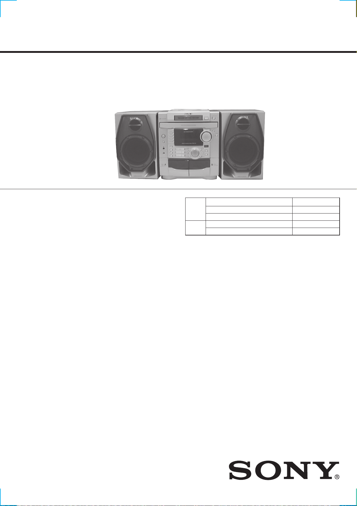
PHC-Z10
SERVICE MANUAL
Ver 1.1 2001. 12
CD
Section
TC
Section
AEP Model
UK Model
Model Name Using Similar Mechanism NEW
CD Mechanism Type KSM-213CCM
Optical Pick-up Name KSS-213C
Model Name Using Similar Mechanism NEW
Tape Transport Mechanism Type MF-PHCZ10T
SPECIFICATIONS
CD player section
System
Compact disc digital audio system
Laser diode properties
Material: GaAlAs
Wave length: 780 nm
Emission duration: Continuous
Laser output: Less than 44.6 µW
(This output is the value measured at a distance of
about 200 mm from the objective lens surface on
the optical pick-up block with 7 mm aperture.)
Spindle speed
200 r/min (rpm) to 500 r/min (rpm) (CLV)
Number of channels
2
Frequency response
20 - 20 000 Hz +1/–2 dB
Wow and flutter
Below measurable limit
Radio section
Frequency range
FM: 87.5 - 108 MHz
AM: 531 - 1 602 kHz
IF
FM: 10.7 MHz
AM: 450 kHz
Aerial
FM: Lead aerial
AM: Loop aerial
Cassette-corder section
Recording system
4-track 2 channel stereo
Fast winding time
Approx. 100 s (sec.) with Sony cassette C-60
Frequency response
TYPE I (normal): 100 - 10 000 Hz
— Continued on next page —
9-929-256-32
2001L1600-1
© 2001.12
PERSONAL COMPONENT SYSTEM
Sony Corporation
Home Audio Company
Published by Sony Engineering Corporation

General
Speaker
Woofer: 13 cm (5
Tweeter: 5 cm (2 inches) dia.,
6 Ω, cone type (2)
Inputs
LINE IN jacks (2 phono jacks):
Sensitivity 220 mV
Outputs
Headphones jack (stereo minijack):
For 8 - 32 Ω impedance headphones
Speaker terminals: For supplied 6 Ω
impedance speaker
Maximum power output
100 W
Power requirements
For personal component system:
230 V AC, 50 Hz
For remote control: 3 V DC, 2 R6 (size AA)
batteries
Power consumption
AC 110 W
Dimensions
Player: approx. 285 × 322 × 408 mm (w/h/d)
(11
Speaker: approx. 200 × 316 × 230 mm (w/h/d)
Mass
Player: approx. 7.7 kg (16 lb. 16 oz.)
Speaker: approx. 2.95 kg (6 lb. 8 oz.)
Supplied accessories
Remote control (1)
FM lead aerial (1)
AM loop aerial (1)
1
⁄8 inches) dia.,
1
⁄4 × 12 3⁄4 × 16 1⁄8 inches)
7
⁄8 × 12 1⁄2 × 9 1⁄8 inches)
(7
CAUTION
Use of controls or adjustments or performance of procedures
other than those specified herein may result in hazardous
radiation exposure.
Flexible Circuit Board Repairing
• Keep the temper ature of the soldering iron around 270˚C during
repairing.
• Do not touch the soldering iron on the same conductor of the
circuit board (within 3 times).
• Be careful not to apply force on the conductor when soldering
or unsoldering.
Notes on Chip Component Replacement
• Never reuse a disconnected chip component.
• Notice that the minus side of a tantalum capacitor may be dam-
aged by heat.
NOTES ON HANDLING THE OPTICAL PICK-UP BLOCK
OR BASE UNIT
The laser diode in the optical pick-up block may suffer electrostatic
breakdown because of the potential difference generated by the
charged electrostatic load, etc. on clothing and the human body.
During repair, pay attention to electrostatic breakdo wn and also use
the procedure in the printed matter which is included in the repair
parts.
The flexible board is easily damaged and should be handled with
care.
Design and specifications are subject to change without
notice.
NOTES ON LASER DIODE EMISSION CHECK
The laser beam on this model is concentrated so as to be focused on
the disc reflective surface by the objective lens in the optical pickup block. Therefore, when checking the laser diode emission,
observe from more than 30 cm away from the objective lens.
SAFETY-RELATED COMPONENT WARNING!!
COMPONENTS IDENTIFIED BY MARK 0 OR DOTTED LINE WITH
MARK 0 ON THE SCHEMATIC DIAGRAMS AND IN THE PARTS
LIST ARE CRITICAL TO SAFE OPERATION. REPLACE THESE
COMPONENTS WITH SONY PARTS WHOSE PART NUMBERS
APPEAR AS SHOWN IN THIS MANUAL OR IN SUPPLEMENTS
PUBLISHED BY SONY.
SERVICE NOTE
When the CD block is going to be inspected, be sure to
connect beforehand the jig (J-2501-020-A) between the CD
board (CNP706) and the DISPLAY board (CNP802).
2

TABLE OF CONTENTS
1. GENERAL
Displaying the spectrum analyzer ...........................................5
Setting the clock ...................................................................... 5
2. DISASSEMBLY
2-1. Side Plate............................................................................. 6
2-2. Cabinet, Rear....................................................................... 6
2-3. Changer Assy, Front ............................................................ 7
2-4. Key (A) Board, Key (B) Board and LED Board ................. 7
2-5. Display Board ..................................................................... 8
2-6. Cassette Mechanism Deck .................................................. 8
2-7. Main Board and Transformer, Power .................................. 9
2-8. CD Mechanism Deck .......................................................... 9
2-9. Base, Changer ...................................................................10
2-10. Optical Pick-up ............................................................... 10
3. MECHANICAL ADJUSTMENTS............................... 11
4. ELECTRICAL ADJUSTMENTS
Tape Section .......................................................................... 11
CD Section ............................................................................13
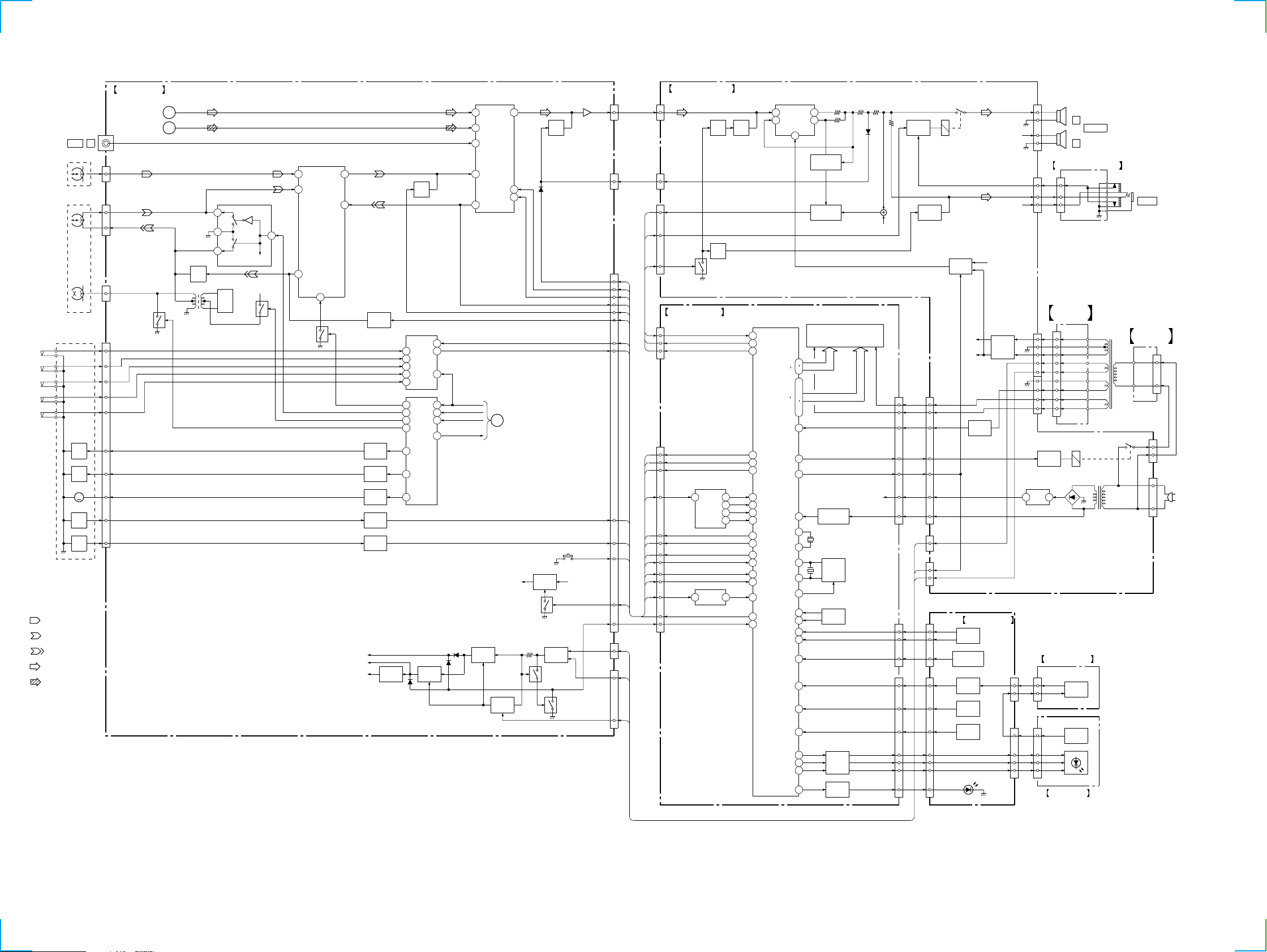
5. DIAGRAMS
5-1. Circuit Boards Location .................................................... 15
5-2. Block Diagram –CD Section–........................................... 17
5-3. Block Diagram –Main Section–........................................ 18
5-4. Printed Wiring Board –Main Section– .............................. 19
5-5. Schematic Diagram –Main Section (1/4)– ........................ 20
5-6. Schematic Diagram –Main Section (2/4)– ........................ 21
5-7. Schematic Diagram –Main Section (3/4)– ........................ 22
5-8. Schematic Diagram –Main Section (4/4)– ........................ 23
5-9. Schematic Diagram –CD Section–.................................... 24
5-10. Printed Wiring Board –CD Section– ................................. 25
5-11. Schematic Diagram –Key Section–................................... 26
5-12. Printed Wiring Board –Key Section– ................................ 27
5-13. Schematic Diagram –Display Section–............................. 28
5-14. Printed Wiring Board –Display Section– .......................... 29
5-15. Schematic Diagram –Power Section– ............................... 30
5-16. Printed W iring Board –Power Section– ............................ 31
5-17. IC Pin Descrption .............................................................. 32
5-18. IC Block Diagrams............................................................ 33
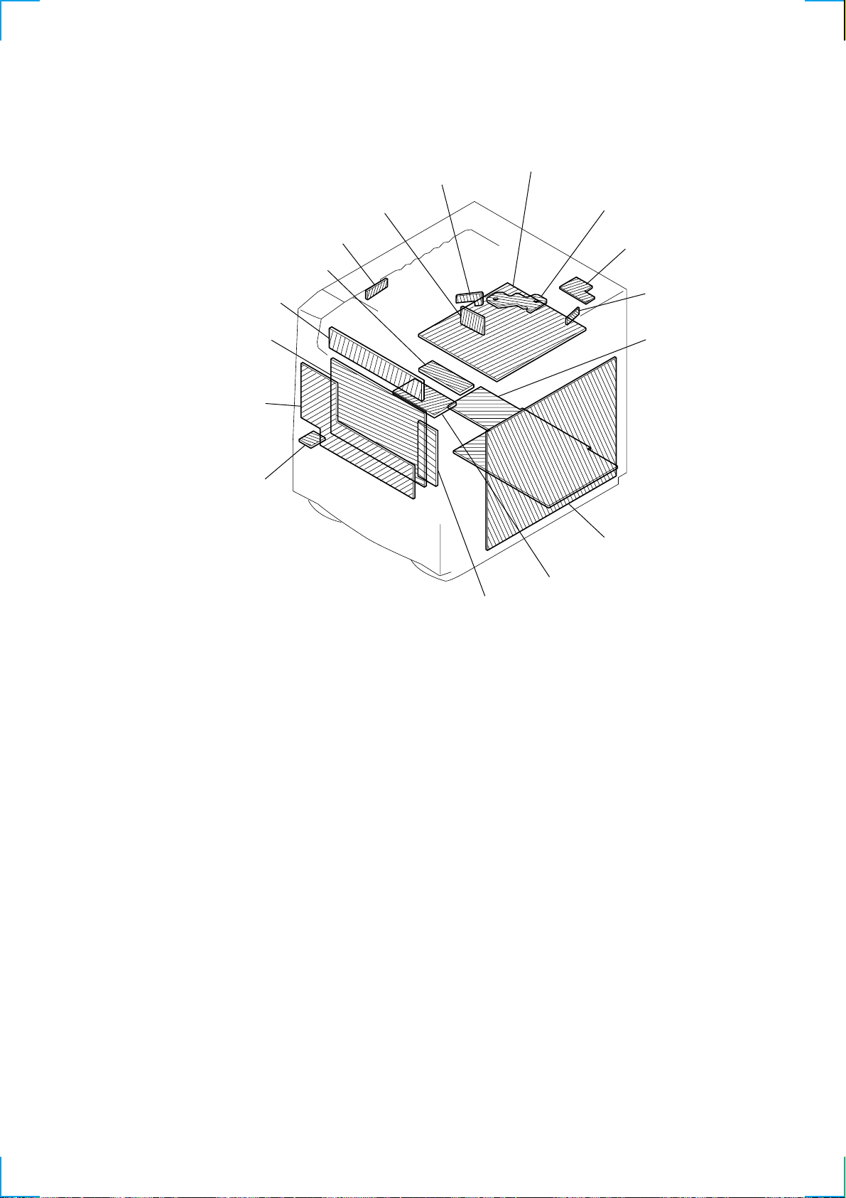
6. EXPLODED VIEWS
6-1. Cabinet Section ................................................................. 38
6-2. Front Cabinet Section........................................................ 39
6-3. Rear Cabinet Section......................................................... 40
6-4. Tape Mechanism Deck Section-1 (MF-PHCZ10)............. 41
6-5. Tape Mechanism Deck Section-2 (MF-PHCZ10)............. 42
6-6. CD Changer Section-1 ...................................................... 43
6-7. CD Changer Section-2 ...................................................... 44
6-8. Optical Pick-up Section (KSM-213CCM) ........................ 45
6-9. Speaker Section ................................................................. 46
7. ELECTRICAL PARTS LIST......................................... 47
3
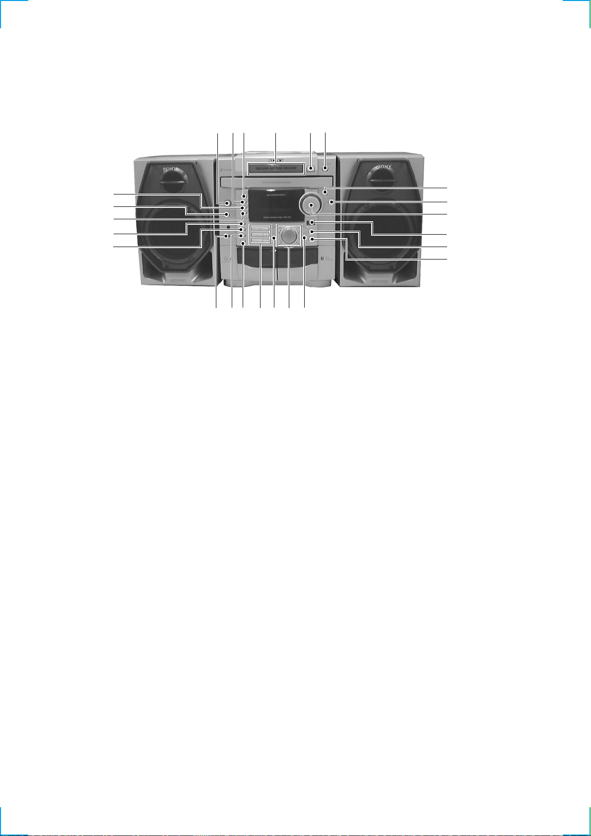
SECTION 1
GENERAL
(L-ch speaker)
wa
w;
ql
qk
qj
1 DISC SELECT indicator
2 DISC CHANGE button
3 OPEN/CLOSE button
4 SOUND button
5 SURROUND button
6 VOLUME knob
7 MEGA BASS button
8 MODE button
9 REPEAT button
0 ENTER button
qa MULTI JOG dial/TUNE +, –,
TAPE m, M button
qs LINE button
qgqh
wfwdws
1
qdqfqa
qs
0
3
2
(R-ch speaker)
qd RADIO/CD x , u /TAPE x , B button
qf DUBBING button
qg z/X button
qh i jack
qj DECK A/B button
qk COUNTER RESET button
ql DISPLAY button
w; SLEEP button
wa CLOCK button
ws POWER button
wd TIMER button
wf STANDBY button
4
5
6
7
8
9
4
This section is extracted
The Audio Emphasis
23
The Audio Emphasis
Displaying the
spectrum analyzer
You can display 3 different patterns of
the audio signal you are listening to by
using the remote.
SPCANL
Displaying the audio signal pattern
Press SPCANL to display the audio signal pattern you
are listening to.
Each time the button is pressed, the display changes.
Choose To display
Peak hold input level of each band and at the same
time the highest level of each band for a
certain moment
Normal input level of each band
Peak the highest level of each band
DECK
A/B
BAND
SPCANL
COUNTER
RESET
LINE
DISC 3DISC 2
CD/RADIO
DISC 1
SURROUND
DISPLAY
SOUND
SLEEP
CLOSE
PO
WER
CD OPEN/
TAPE
TUNERADIO
REPEAT
CD
VOL
The Timer
24
Setting the clock
“- -:- -” indication appears in the
display until you set the clock.
The Timer
Tip
The time display
system:
12-hour system
AM12:00 = midnight
PM12:00 = noon
CLOCK
ENTER
MEM
MULTI JOG
Before you begin, hook up the system (see pages 31 -
34).
1
Press and hold CLOCK until the hour digit flashes.
2
Set the clock.
1 Turn MULTI JOG to
set the hour and
press ENTER MEM.
2 Turn MULTI JOG to
set the minutes.
3
Press ENTER MEM.
The clock starts from 00 seconds.
from instruction manual.
5
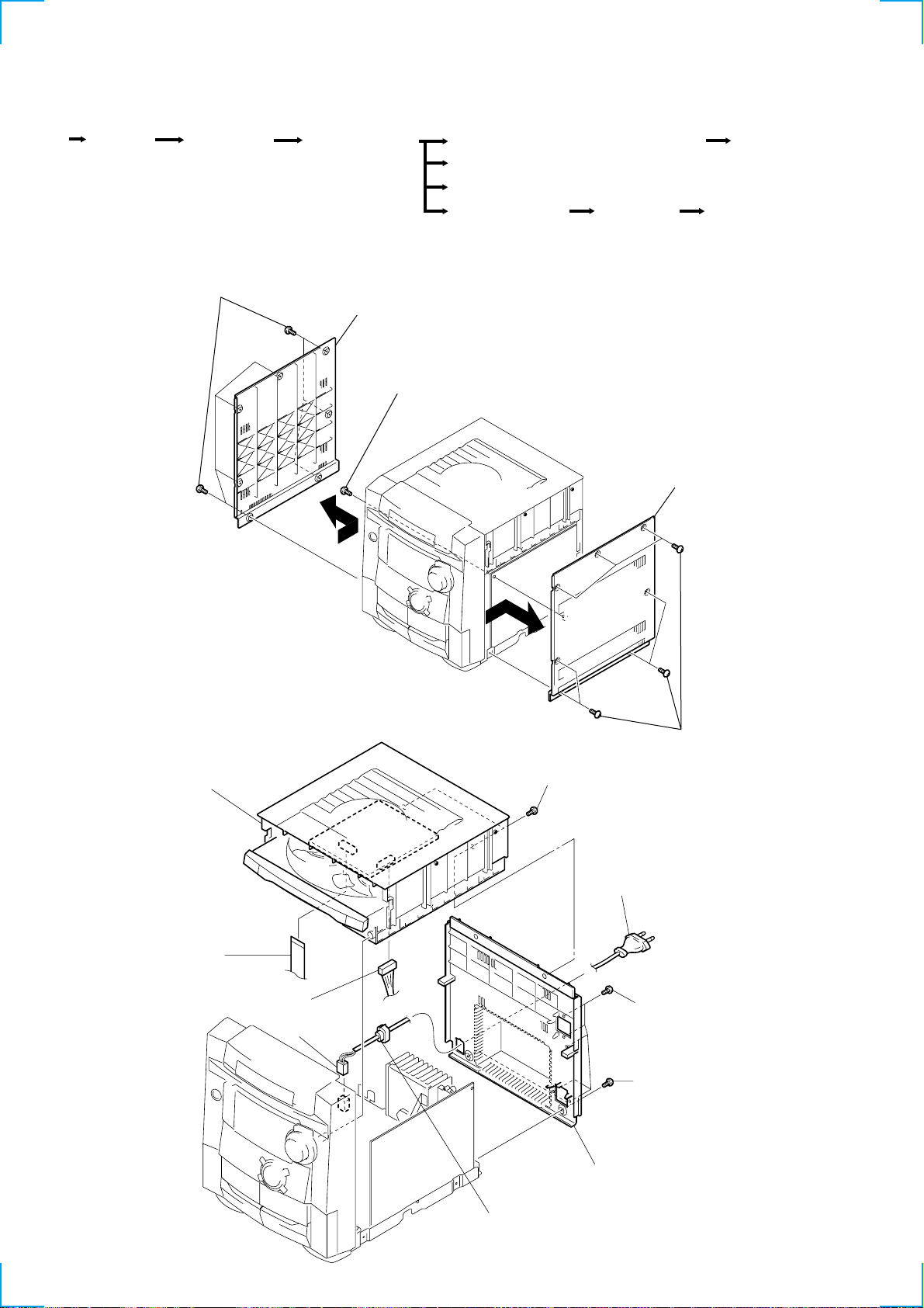
SECTION 2
d
DISASSEMBLY
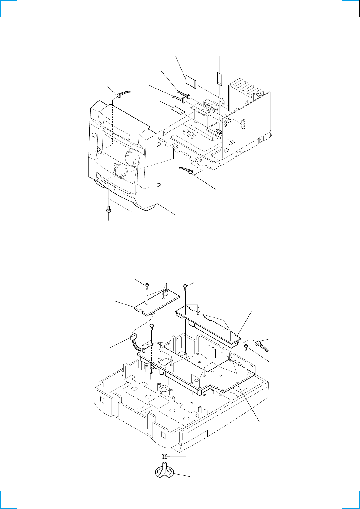
• The equipment can be removed using the following procedure.
Side PlateSet
Cabinet, Rear
Note : Follow the disassembly procedure in the numerical order given.
2-1. SIDE PLATE
1
Seven screws (BTP 3 x 10)
Cabinet assy, front
2
Plate (L), side
3
Screw
Key (A) Board, Key (B) Board and LED Board
Cassette Mechanism Deck
Main Board and Transformer, Power
CD Mechanism Deck
(+P 3 x 10)
Charger Base
5
Display Boar
Optical Pick-Up
Plate (R), side
2-2. CABINET, REAR
4
Cabinet, top and
CD mechanism
1
CNP706
2
CNP705
7
CNP903
Two screws
3
(+P 3 x 10)
4
Seven screws (BTP 3 x 10)
Cord, power
9
5
Five screws
(BTP 3 x 10)
6
Two screws
(BTP 3 x 10)
0
Cabinet, rear
8
Stopper, AC cord
6
2-3. CABINET ASSY, FRONT
7
CNP906
8
Two screws
(+PTT 3 x 10)
CNP302
3
4
CNP307
2
CNP301
1
CNP303
9
Cabinet assy, front
6
CNP909
5
CNP310
2-4. KEY (A) BOARD, KEY (B) BOARD AND LED BOARD
1
3
Key (B) board
9
Eight Screws
(+P 2.6 x 8)
2
CNP808
Three screws (+P 2.6 x 8)
4
Five screws
(+P 2.6 x 8)
6
LED board
qa
Key (A) board
5
CNP809
0
Nine Screws
(+P 2.6 x 8)
8
Nut
7
Button, select
7
2-5. DISPLAY BOARD
3
Two screws
(+P 2.6 x 8)
7
5
CNP801-1
Display board
Two screws
4
(+P 2.6 x 8)
6
CNP801-2
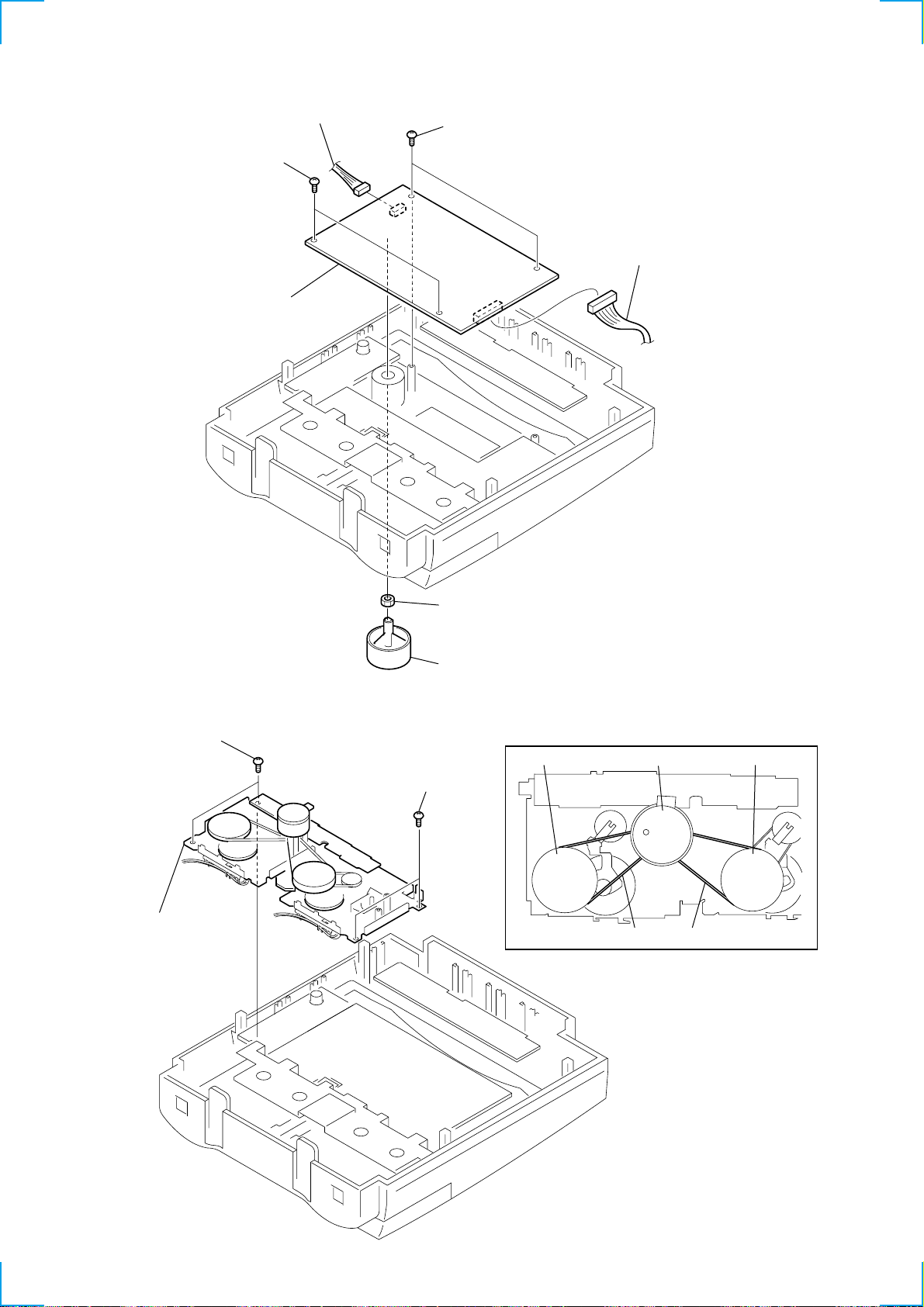
2-6. CASSETTE MECHANISM DECK
1
Two screws
3
Cassette mechanism deck
(+P 3 x 10)
2
1
2
Two screws
(+P 3 x 10)
Nut
Button, VOL
Belt threading
Flywheel (B)
Capstan motor
Belt
Belt
Flywheel (A)
8
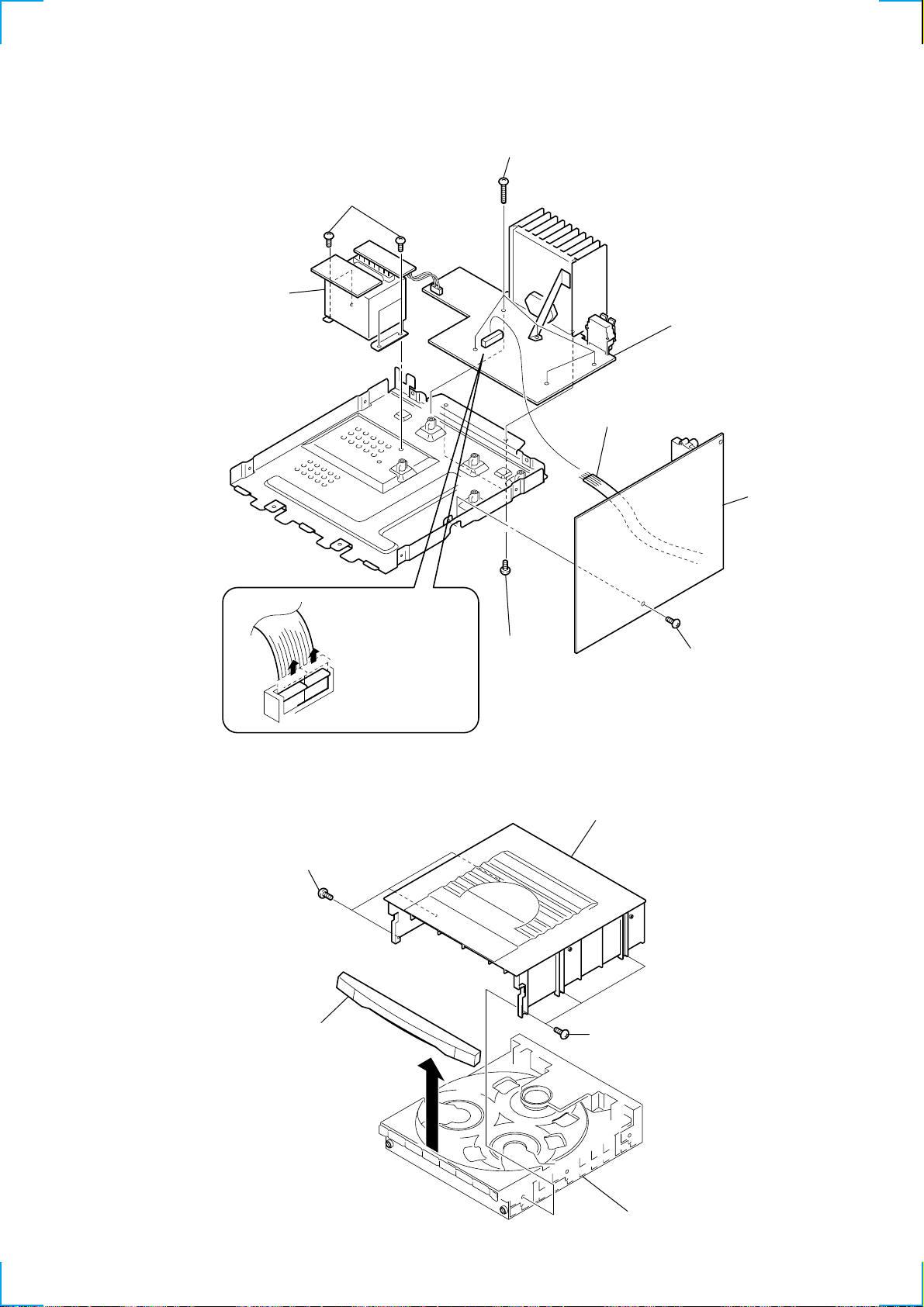
2-7. MAIN BOARD AND TRANSFORMER, POWER
6
Five screws (+BVTT 3 x 20)
7
Four screws
(+BVTT 4 x 6)
Transformer,
8
power (T901)
2
Harness
9
Amplifier board
4
Main board
2-8. CD MECHANISM DECK
1
Three screws
4
1
(+P 3 x 10)
Door, CD
Release lock of the
connector in the
direction of the arrow.
5
Two
screws
(+PTT 3 x 10)
3
Cabinet, top
2
Three screws
3
Screw
(+PTT 3 x 10)
(+P 3 x 10)
5
CD mechanism deck
9
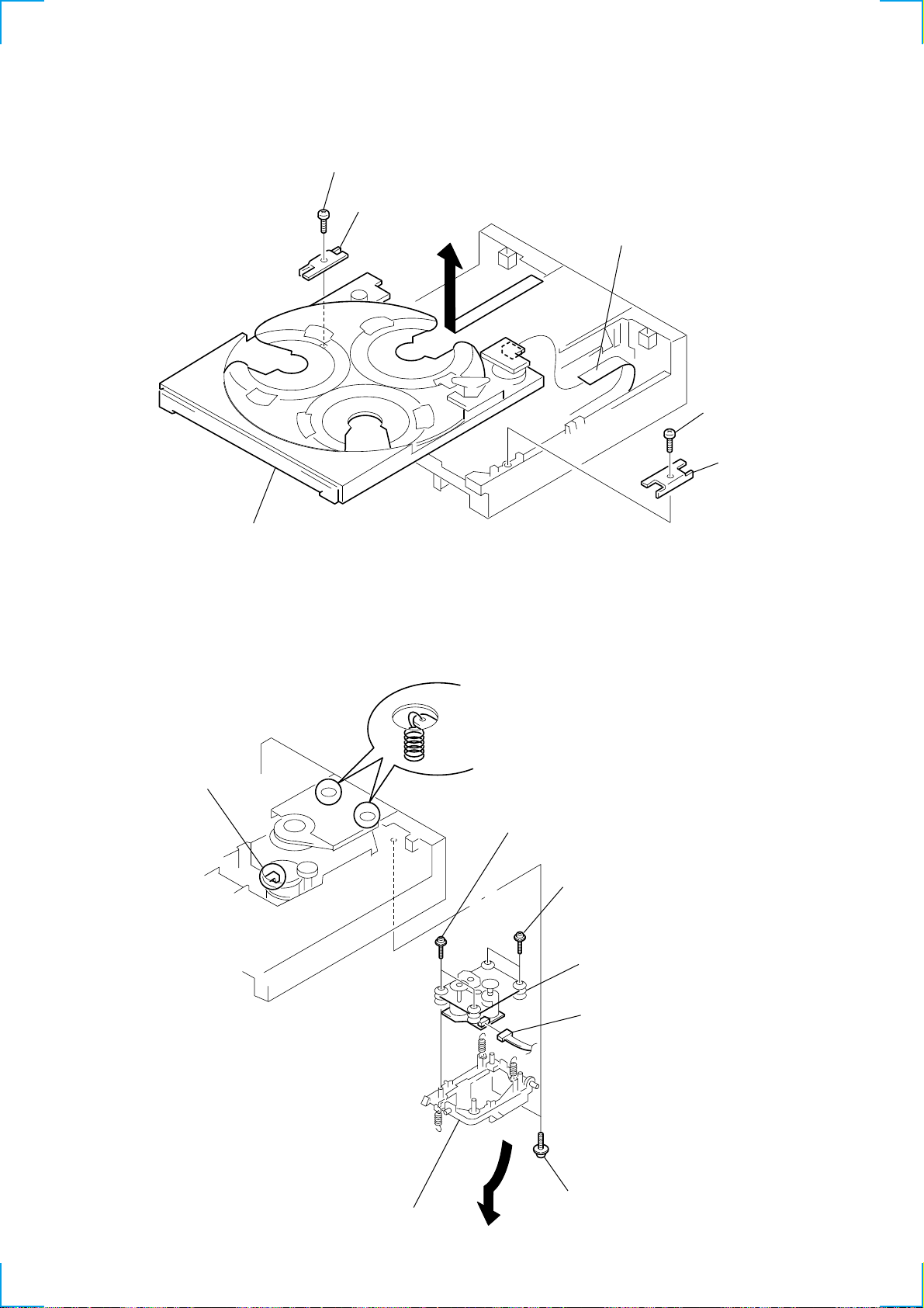
2-9. BASE, CHANGER
7
Base, changer
1
Screw (P 2.6 x 8)
2
Guide, rail
6
5
CN6
3
Screw
(P 2.6 x 8)
4
Guide, rail
2-10. OPTICAL PICK-UP
2
Take off the spring.
1
Take off the spring.
7
Screws tapping, (M2.6 x 20)
8
Screws tapping, (M2.6 x 20)
9
Optical pick-up
3
Connector
10
6
Mechanism assy, CD
5
4
Screws (PTPWH 3 x 8)
SECTION 3
R-CH
peak
R-CH
peak
L-CH
peak
L-CH
peak
screw
position
Output
level
within
1 dB
within
1 dB
angle
MECHANICAL ADJUSTMENTS
SECTION 4
ELECTRICAL ADJUSTMENTS
PRECAUTION
1. Clean the following parts with a denatured alcohol-moistened
swab :
record/playback head capstan idlers
playback head pinch roller
erase head rubber belts
2. Demagnetize the record/playback head with a head
demagnetizer. (Do not bring the head demagnetizer close to the
erase head.)
3. Do not use a magnetized screwdriver for the adjustments.
4. After the adjustments, apply suitable locking compound to the
parts adjusted.
5. The adjustments should be performed with the rated power
supply voltage unless otherwise noted.
Torque Measurement DECK A DECK B
Mode Torque meter Meter reading
2.21– 5.39 mN • m
Forward
Forward
back tension
Fast Forward
and Rewind
CQ-102C
CQ-102C
CQ-201B
Tape Tension Measurement DECK A DECK B
Mode Tension meter Meter reading
Forward CQ-403A
(22.5 to 55 g • cm)
(0.31 to 0.76 oz • inch)
0.20 – 0.49 mN • m
(2 to 5 g • cm)
(0.03 to 0.07 oz • inch)
5.88 – 11.77 mN • m
(60 to 120 g • cm)
(0.83 to 1.67 oz • inch)
more than 150 g
(more than 5.29 oz)
TAPE SECTION 0 dB = 0.775 V
Standard Output Level
Output terminal SP OUT PHONES OUT
load impedance 6 Ω 32 Ω
output signal level 0.775 V (0 dB) 0.25 V (–10 dB)
Test T ape
Tape Signal Used for
WS-48B 3 kHz, 0 dB tape speed adjustment
P-4-A063 6.3 kHz, –10 dB head azimuth adjustment
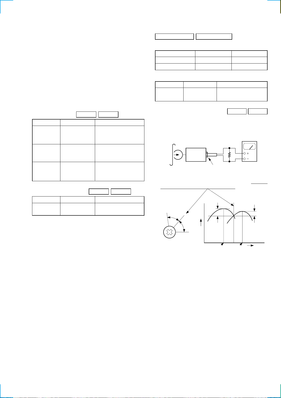
REC/PB Head Azimuth Adjustment DECK A DECK B
Procedure:
1. Mode: playback
test tape
P-4-A063
(6.3 kHz, –10 dB) level meter
32 Ω
set
J901 (phones)
2. Turn the adjustment screw for the maximum output levels. If
these levels do not match. Turn the adjustment screw until both
of output levels match together within 1 dB.
11
y
3. Phase Check
Mode: playback
test tape
P-4-A063
(6.3 kHz, –10 dB)
L-CH
set
L-CH
32 Ω
osilloscope
VH
Tape Speed Adjustment DECK A DECK B
Procedure:
Mode: Playback
test tape
WS-48B
(3 kHz, 0 dB)
set
digital frequenc
counter
0000
32 Ω
R-CH
in phase 45˚ 90˚ 135˚ 180˚
32 Ω
R-CH
J901 (phones)
Screen pattern
good wrong
Note: Finish the screw adjustment with a turn in the clockwise
direction.
After the adjustment, lock the adjustment screw.
Adjustment Location: playback head (deck A)
record/playback head (deck B)
J901 (phones)
Adjustment V alue: normal tape speed
Adjust the tape speed adjustment control inside motor, so that the
frequency counter reading becomes 3,000 Hz.
Specification V alue:
Digital frequency counter
2,910 – 3,090Hz
Frequency difference between the beginning and the end of the tape
should be within 1.5% (45 Hz).
Adjustment Location:
CASSETTE DECK
adjustment screw
Tape speed adjustment
control inside motor
Sample Value of Wow and flutter
W.RMS (JIS) less then 0.3%
(test tape: WS-48B)
12
TUNER SECTION 0 dB = 1 µV
)
• FM Section
Setting:
BAND switch: FM
FM RF signal
generator
antenna terminal
0.01 µF
set
22.5 kHz frequency
deviation by 1 kHz signal
Output level : as low as possible
FM FREQUENCY COVERAGE
CHECK
Frequency Display 87.5 MHz 108 MHz
Reading on Digital voltmeter 1.65 ± 0.15V 4.0 ± 0.2 V
Adjustment Part <confirmation> <confirmation>
FM TRACKING CHECK
Adjust for a maximum reading on level meter.
<confirmation> <confirmation>
87.5 MHz 108 MHz
• AM Section
Setting:
BAND switch: AM
AM RF signal
generator
Put the lead-wire
antenna close to
the AM loop
antenna.
30% amplitude
modulation by 400 Hz signal
Output level : as low as possible
• Connecting Level Meter (FM and AM)
level meter
(range: 0.5-5 V ac
32 Ω
set
J901 (phones)
AM IF ADJUSTMENT
Adjust for a maximum reading on level meter.
CFT1
450 kHz
AM FREQUENCY COVERAGE
ADJUSTMENT
Frequency Display 531 kHz 1,611 kHz
Reading on Digital voltmeter 0.75 ± 0.15 V 5.4 ± 0.2 V
Adjustment Part L5 <confirmation>
AM TRACKING ADJUSTMENT
Adjust for a maximum reading on level meter.
L3 CT1
621 kHz 1,404 kHz
Adjustment Location: See page 14.
• Connecting Digital Voltmeter (FM and AM)
digital
voltmeter
100 kΩ
TP1 (VT)
• Repeat the procedures in each adjustment several times, and the
frequency coverage and tracking adjustments should be finally
done by the trimmer capacitors.
13
Adjustment Location: main board
G
[MAIN BOARD] (conductor side)
L5
AM FREQUENCY
COVERAGE
adjustment
TP1
(VT)
CT1
AM TRACKING
adjustment
IC1
L3
AM TRACKIN
adjustment
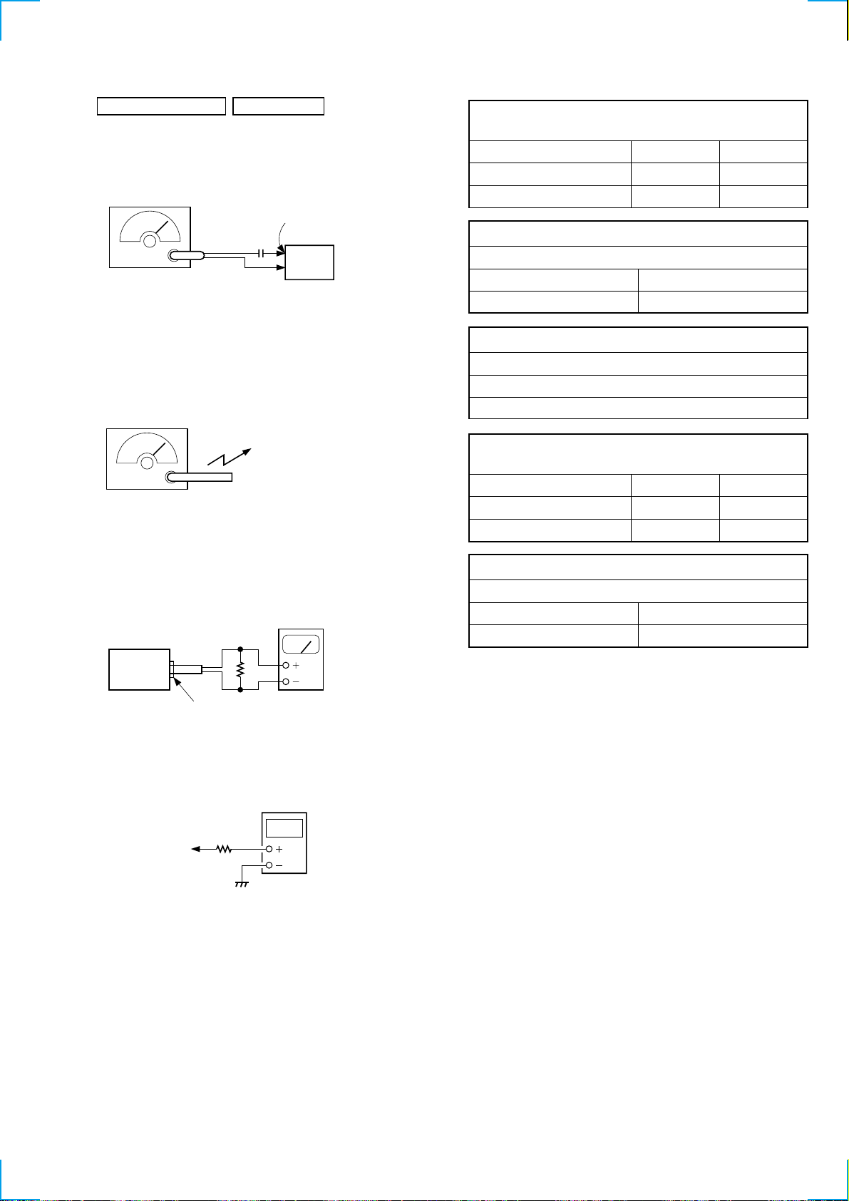
CD SECTION
CD section adjustments are done automatically in this set.
In case of operation check, confirm that focus bias.
SERVICE NOTE
When the CD block is going to be inspected, be sure to
connect beforehand the jig (J-2501-020-A) between the CD
board (CNP706) and the DISPLAY board (CNP802).
FOCUS BIAS CHECK
1. Connect the oscilloscope between IC701 pin #£ (TP RFO) and
GND on Main board.
2. Insert the disc (YEDS-18). (Part No. : 3-702-101-01)
3. Press the CD ^ button.
4. Confirm that the oscilloscope waveform is as shown in the
figure below. (eye pattern)
A good eye pattern means that the diamond shape ( ) in the
center of the waveform can be clearly distinguished.
• RF signal reference waveform (eye pattern)
VOLT/DIV : 200 mV (10 : 1 probe in use)
TIME/DIV : 500 nS
π
Test Point:
[CD BOARD] (conductor side)
TP (RF0)
R720
IC701
RF level :
1.3 ± 0.5 Vp-p
When observing the eye pattern, set the oscilloscope for AC range
and raise vertical sensitivity.
14
5-1. CIRCUIT BOARDS LOCATION
SECTION 5
DIAGRAMS
POWER(A) board
LED board
DISPLAY board
KEY (A) board
HEADPHONE board
LOAD SW board
O/C SW board
DISC COUNT SW board
CD board
CD MOTOR board
MOTOR board
DISC STOP SW board
AMPLIFIER board
MAIN board
POWER(B) board
KEY(B) board
15

Note on Printed Wiring Board:
• X : parts extracted from the component side.
• Y : parts extracted from the conductor side.
• b : Pattern from the side which enables seeing.
Note on Schematic Diagrams:
• All capacitors are in µF unless otherwise noted. pF: µµF
50 WV or less are not indicated except for electrolytics
and tantalums.
• All resistors are in Ω and 1/
specified.
f
•
: internal component.
4
W or less unless otherwise
• 2 : nonflammable resistor.
• 5 : fusible resistor.
• C : panel designation.
• H : adjustment for repair.
• U : B+ Line.
• Power voltage is dc 9 V and fed with regulated dc po wer
supply from battery terminal.
• Voltages and waveforms are dc with respect to ground
Note: The components identified by mark 0 or dotted line
with mark 0 are critical for safety.
Replace only with part number specified.
under no-signal (detuned) conditions.
– For Radio, TAPE section MAIN (1/2) –
No mark : FM
( ) : AM
< > : CD PLAY
[ ] : TAPE PLAY
• V oltages are taken with a VOM (Input impedance 10 MΩ).
Voltage variations may be noted due to normal production tolerances.
• Signal path.
F : FM
f : AM
E : PB
a : REC
J : CD
16
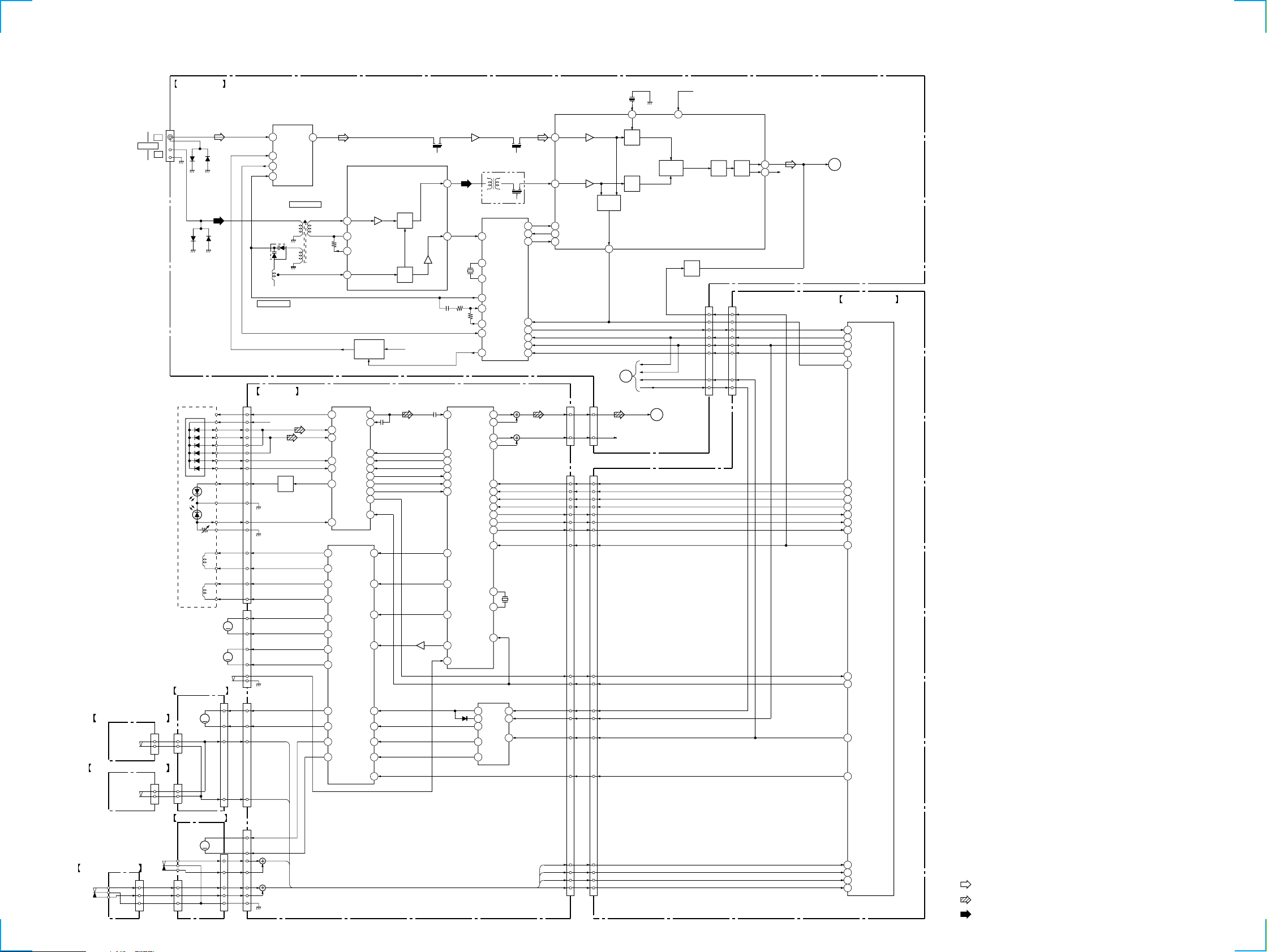
5-2. BLOCK DIAGRAM – CD SECTION –
PHC-Z10
DISC STOP SW BOARD
SW704
TT POST
DISC COUNT SW BOARD
SW703
DISC COUNT
LOAD SW BOARD
OPEN
CLOSE
SW701
CNP714
16
ANTENNA
CNP710
CNP712
3
1
2
DOWN
UP
MAIN BOARD
FM
AM
OPTICAL PICK-UP
BLOCK
(KSS-213C)
VR
FOCUS
COIL
TRACKING
COIL
MOTOR BOARD
M701
DISC
MOTOR
CNP711
1 1
22
CNP709
1 1
22
O/C SW BOARD
M702
TRAY
MOTOR
SW702
CNP713
3
1
2
VC
A
B
C
D
E
F
LD
GND
PD
F+
F-
T+
T-
SLED
MOTOR
SPINDLE
MOTOR
CNP702
M
CNP708
M
(1/2)
M
M
LIMIT
SW
4
5
2
3 3
4
5 5
1
2
3
10
12
11
13
16
15
14
1
2
5
6
7
4
3
8
9
3
4
1
2
5
6
4
5
2
6
7
4
1
2
3
CNP701
CNP705
CNP707
CNP703
L5
MW OSC
TUNER 5V
AM FREQ. COV.
CD BOARD
C COUNT
FM TUNER PACK
RF IN
1
6
VDD
8
OSC OUT
5
VT
D3
+5V
Q701
LD
DRIVE
C STOP
C UP/DN
C CL/OP
TU1
IF OUT
7 1
AM/FM IF, MPX
IC1(1/2)
AM TRACKING
L3
MW ANT
21
22
3
23
RF AMP
IC701
51
VC
38
PD1
39
PD2
42
E
41
F
36
LD
37
PD
MOTOR/COIL DRIVE
IC702
18
OUT4+
17
OUT4-
20
OUT5+
19
OUT5-
2
OUT1+
1
OUT1-
3
OUT2+
4
OUT2-
30
OUT6+
31
OUT6-
14
OUT3+
15
OUT3-
AM RF IN
AFC
REG
AM OSC
RFO
RFI
DATA
SENS1
SENS2
XRST
IN6F
IN6R
IN3F
IN3R
MUTE
+B SW
Q8,Q10
IN4
IN5
IN1
IN2
33
32
22
20CLK
21XLT
27FOK
24COUT
25
26
23
22
21
6
5
29
28
13
12
27
CF1
10.7MHz
MIX OUT
AM
MIX
OSC OUT
AM
OSC
8.5V
IC705
Q9
AMP
2
24
35
12
14
13
18
11
10
13
16
21
15
12
21
X1
75kHz
20
19
18
17
13
DIGITAL SERVO
DIGITAL SIGNAL PROC.
D/A CONV.
IC703
L OUT1
RF
A OUT1
L OUT2
A OUT2
DATO
CLKO
XLTO
FOK
CNIN
CLK
SEIN
XLAT
SQCK
SCOR
SQSO
SENS
SMUTE
6
FEO
TAO
SLO
XRST
MDP
SPOA(LIMIT)
6
14
7
4
5
CFT1
AM IFT
PLL
IC2
AM-IN
XOUT
XIN
LP OUT
LP IN
PD
FM-IN
6
MW=H
67
65
74
76
7DATA
9
8
4
57
5
6
62
71XTAI
72XTAO
79
IC704
LEVEL
SHIFT
CF2
10.7MHz
MO/ST
ST IND
BAND
(FM=H)
IF IN
DO
DI
CK
CE
16.9344MHz
2
3
1
14 12
9
8
11
5
3
4
2
X701
CNP704
CNP706
C STOP
C COUNT
C UP/DN
C CL/OP
4
MO/ST
ST OUT
7
BAND
11
AM/FM IF, MPX
IC1(2/2)
FM IF IN
AM IF IN
3
1 1
13
11
9
12
15
10
14
3
8
1
5
17
4
2
18
16
7
6
13
11
12
15
10
14
17
18
16
3
9
3
8
1
5
4
2
7
6
BUFFER
SECTION
CNP309
CNP802
CF3
10,7MHHz
IF
IFOUT
10
TC
R-ch
TUNER 5V
8
FM-DET
FM
DET
AM
DET
C
CD-L
RDATA
RCLK
STB
DI
9
VCC
FM/AM
BUFFER
B-MUTE
TC
B
SECTION
MUTE
IF-REQ
R-CLK
R-CE
Q12
CNP303
(1/2)
DO
DI
FM
MPX
7
20
18
19
10
9
23
13
MUTE
14
CNP803
7
(1/2)
20
18
19
10
9
23
TU-L
R-ch
TC
A
SECTION
DISPLAY BOARD
SYSTEM CONTROL
IC801(1/2)
9
R DATA IN
11
R DATA OUT
10
R CLK
47
R CE
23
IF-REQ
52
C DATA
51
C CLOCK
50
C LATCH
25
C SQCK
6
C SCOR
26
C SQSO
24
C SENS
56
B MUTE
27
C SENS2
53
C XRST
49
STB
55
CD PLAY
15
C STOP
20
C COUNT
29
C UPDWN
30
C CLOP SW
(1/2)
• R-ch is omitted due to same as L-ch.
• Signal Path
: FM
: CD
: AM
1717
PHC-Z10
5-3. BLOCK DIAGRAM – MAIN SECTION –
DECK-A
PB
HEAD
DECK-B
REC/PB
HEAD
ERASE
HEAD
CASSETTE DECK
MECHANISM
A HALF
A HEAD
B HALF
B HEAD
REC FWD
SOL
SOL
P DET
P DET
• R-ch is omitted due to
same as L-ch.
• Signal Path
: PB (DECK A)
: PB (DECK B)
: REC (DECK B)
: FM
: CD
MAIN BOARD
LAUX
CNP301
1
CNP302
5
4
CNP310
2
CNP307
12
10
9
1
13
6
A
5
B
4
M
8
A
3
B
16
TUNER
SECTION
SECTION
Q308
(2/2)
TU-L
A
CD-L
CD
B
DECK A/B SELECT
PB/REC EQ AMP
IC305
24
PRE OUT
BIAS
TRAP
L306
REC/PB SWITCH
9
8
7
BIAS
OSC
Q309
IC304
Q310
Q311
R ch
A+8V
CH2A
23
CH2B
4
16
REC OUT2
Q314
A/B SW
19
REC IN2
20
14
MAIN +5V
+12V
+9V
REC MUTE
Q305
SOL A
DRIVE
Q319,320
SOL B
DRIVE
Q317,318
MOTOR
DRIVE
Q315,316
BUFFER
Q324
BUFFER
Q325
+5V REG
Q914
13
3
4
11
14
4
14
11
12
5
7
6
MUTE
Q304
IC306
SHIFT
REGISTER
IC307
SHIFT
REGISTER
+9V REG
Q911,912
1
9
2
3
2
1
10
SURROUND PROC.
5
4
7
6
8
RCLK
RDATA
STB
DI
+12V REG
Q909,910
IC301
L OUT
LIN2
27
LIN1
LIN4
LIN3
22SDA
D303
21SCL
MUXO-L
TUNER
SECTION
C
S301
RESET
Q323
+B SW
Q322
D906-909
Q905
TUNER +5V MAIN +5V
POWER
CONT
Q907,908
MUTE
Q102
RECT
Q906
CNP305A
(1/2)
IC303
31
CNP305B
(1/2)
DIST
CNP303
(2/2)
MBAS
VDATA
VCLK/VER
SPEANA
165SL
165QH
T -A COUNT
T-B COUNT
RESET
RADIO
SFTY
CNP305A
(2/2)
CNP305B
(2/2)
PCON
1
L
4
3
15
14
1
4
PM
5
RM
8
16
22
21
13
6
17
5
AC
1
AC
3
AMPLIFIER BOARD
CNP908
(1/2)
1
L
CNP910
(1/2)
4
DIST
CNP909
(1/2)
5
PROT
7
SRELAY
10
AMUTE
DISPLAY BOARD
CNP804
(1/2)
5
PROT
7
SRELAY
10
A MUTE
CNP803
(2/2)
3
MBAS
15
VDATA
14
VCLK/VER
1
SPEANA
4
PM
5
RM
8
165SL
16
165QH
22
T-A COUNT
21
T-B COUNT
13
RESET
6
RADIO
17
SFTY
POWER AMP
IC902
15
OUT2-
IN2
NF2
VFDP
PSAVE
PCON
XTAL
EXTAL
R SHFT
VOL1
VOL2 17
JOG1
JOG2
KEY1 34
KEY2
KEY3
DISC1
DISC2
DISC3
REF-VSS
12
P1
P18
G1
G14
TEX
TX
OUT2+
87
70
2
.
1
.
100
90
.
88
45
54
58
7
43
42
40
39
46
16
18
19
8
35
36
67
68
69
63
X802
8MHz
11
10
OVER LOAD
DETECT
Q104
Q104
PROTECTOR
Q917-919
REG CHECK
X801
32.768kHz
CONTROL
Q801,802
VOLUME
FL801
LIQUID CRYSTAL
DISPLAY PANEL
Q807
OSC
SW801
Q804-806
LED
DRIVE
Q803
LED
DRIVE
D904
+5.6V
R-ch
CNP804
(2/2)
FL2
FL1
-35V
PSAVE
PCON
AC IN
CNP801-1
CNP801-2
3
2
1
3
2
1
6
7
8
5
MUTE
MUTE
CONT
Q103
Q916
MUTE
CONT
Q915
Q922
(2/2)
SPEANA
(B.P.F)
IC803
8
AOUT
AIN
17
A
10
B
11
C
12
RESET
1
3
IC804
14
SYSTEM CONTROL
IC801(2/2)
12
PROT
62
SRELAY
57
AMUTE
23
MBASS
31
VDATA
32
VCLK/VER
33
SPANA
64
SPN A
65
SPN B
REG CHK
66
SPN C
61
PM
60
RM
48
165SL
14
165QH
4
T-A COUNT
5
T-B COUNT
38
RST
59
RADIO
13
SATY
MBASS LED
REMOTE
RELAY
DRIVE
Q920,921
MUTE
Q105,106
33
22
11
1111
99
66
44
5
3
1
3
2
1
3
2
1
6
7
8
5
RY902
CNP909
(2/2)
FL2
FL1
-35V
PSAVE
PCON
+5.6V
ACIN
CNP908
(2/2)
AC
CNP910
(2/2)
PCON
AC
CNP805-1
CNP805-2
SWITCH
Q901-903
+B
-B
-35V REG
KEY(A) BOARD
JOG
IC802
REMOTE
CONTROL
RECEIVER
SW823-828
FUNCTION
KEY
SW813-822
FUNCTION
KEY
SW803-812
FUNCTION
KEY
LED801
Q923
+12V
D902
RECT
CNP807
CNP806
R ch
R ch
131
4 4
1
2
3
CNP907
CNP904
CNP904A
3
+
-
+
-
HEADPHONE BOARD
1
1
2
2
4
4
POWER(B)
BOARD
CNP901
1
1
22
3
3
4
4
55
6
1
7
2
8
3
9
4
RELAY
DRIVE
Q904
D910-913
IC901
+5.6V
1
REG
KEY(B) BOARD
CNP808
3
CNP809
1
2
3
LED BOARD
SP901
L
SP902
R
CNP906
RY901
SW829,830
FUNCTION
KEY
SW831,832
FUNCTION
KEY
LED802-807
J902
SPEAKER
POWER
TRANSFOMER
T901
POWER
TRANSFOMER
T902
J901
PHONES
POWER(A)
BOARD
CNP905
2
1
CNP902
1
2
1
2
CNP903
AC
IN
1818
 Loading...