

Page 1
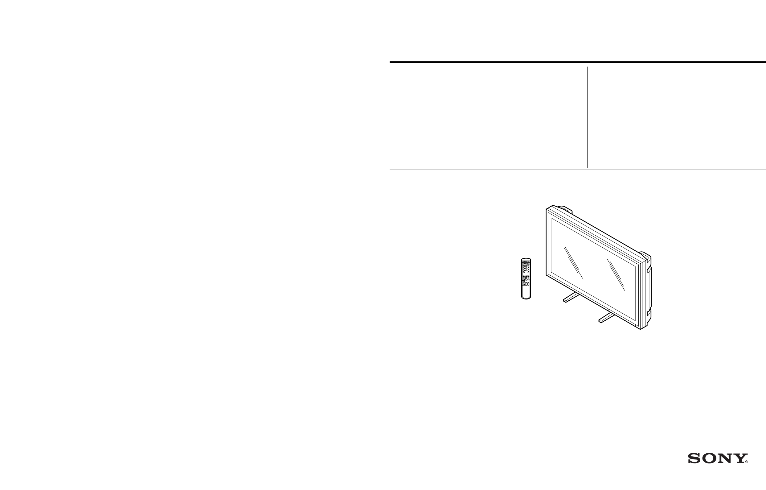
SERVICE MANUAL
MODEL
.............. ......... ....................
DEST. CHASSIS NO. MODEL DEST. CHASSIS NO.
PFM-500A3WE AEP
PFM-500A3WG E
PFM-500A3WU US/CND
PFM-510A2WE AEP
PFM-510A2WG E
PFM-510A2WU US/CND
.............. ......... ....................
BKM-500
MB-514
RM-921
PFM-500A3W/510A2W Flat Panel Monitor
BKM-500 Input Adaptor
MB-514 Mounting Bracket
RM-921 Remote Commander
English
00DY16110-1
Sony Corporation
Communication System Solutions Network Company9-929-680-01
Printed in Japan
©2000.4
FLAT PANEL MONITOR
Page 2
! WARNING
This manual is intended for qualified service personnel only.
To reduce the risk of electric shock, fire or injury, do not perform any servicing other than that
contained in the operating instructions unless you are qualified to do so. Refer all servicing to
qualified service personnel.
! WARNUNG
Die Anleitung ist nur für qualifiziertes Fachpersonal bestimmt.
Alle Wartungsarbeiten dürfen nur von qualifiziertem Fachpersonal ausgeführt werden. Um die
Gefahr eines elektrischen Schlages, Feuergefahr und Verletzungen zu vermeiden, sind bei
Wartungsarbeiten strikt die Angaben in der Anleitung zu befolgen. Andere als die angegeben
Wartungsarbeiten dürfen nur von Personen ausgeführt werden, die eine spezielle Befähigung
dazu besitzen.
! A VERTISSEMENT
Ce manual est destiné uniquement aux personnes compétentes en charge de l’entretien. Afin
de réduire les risques de décharge électrique, d’incendie ou de blessure n’effectuer que les
réparations indiquées dans le mode d’emploi à moins d’être qualifié pour en effectuer d’autres.
Pour toute réparation faire appel à une personne compétente uniquement.
WARNING!!
AN INSULATED TRANSFORMER SHOULD BE USED DURING
ANY SERVICE TO AVOID POSSIBLE SHOCK HAZARD, BECAUSE OF LIVE CHASSIS.
THE CHASSIS OF THIS RECEIVER IS DIRECTL Y CONNECTED
TO THE AC POWER LINE.
SAFETY-RELATED COMPONENT WARNING !!
COMPONENTS IDENTIFIED BY A
DIAGRAMS, EXPLODED VIEWS AND IN THE P ARTS LIST ARE
CRITICAL TO SAFE OPERATION. REPLACE THESE COMPONENTS WITH SONY P ARTS WHOSE P ART NUMBERS APPEAR
AS SHOWN IN THIS MANUAL OR IN SUPPLEMENTS PUBLISHED BY SONY.
!!
! MARK ON THE SCHEMATIC
!!
ATTENTION!!
AFIN D’ÉVITER TOUT RISQUE D’ÉLECTROCUTION
PROVENANT D’UN CHÂSSIS SOUS TENSION, UN
TRANSFORMATEUR D’ISOLEMENT DOIT ETRE UTILISÉ LORS
DE TOUT DÉPANNAGE.
LE CHÂSSIS DE CE RÉCEPTEUR EST DIRECTEMENT
RACCORDÉ Á L’ALIMENTATION SECTEUR.
ATTENTION AUX COMPOSANTS RELATIFS Á LA
SÉCURITÉ!!
LES COMPOSANTS IDENTIFIÉS PAR UNE MAPQUE
LES SCHÉMAS DE PRINCIPE, LES VUES EXPLOSÉES ET LES
LISTES DE PIECES SONT D’UNE IMPORTANCE CRITIQUE
POUR LA SÉCURITÉ DU FONCTIONNEMENT. NE LES
REMPLACER QUE PAR DES COMPOSANTS SONY DONT LE
NUMÉRO DE PIÈCE EST INDIQUÉ DANS LE PRÉSENT
MANUEL OU DANS DES SUPPLÉMENTS PUBLIÉS P AR SONY .
!!
! SUR
!!
Page 3
Voor de klanten in Nederland
Dit apparaat bevat een CR2025 batterij voor memory
back-up.
CAUTION
Danger of explosion if battery is incorrectly
replaced.
Raadpleeg uw leverancier over de verwijdering van de
batterij op het moment dat u het apparaat bij einde
levensduur afdankt.
Gooi de batterij niet weg. maar lever hem in als KCA.
Bij dit produkt zijn batterijen geleverd.
Wanneer deze leeg zijn, moet u ze niet
weggooien maar inleveren als KCA.
Replace only with the same or equivalent type
recommended by the manufacturer.
Dispose of used batteries according to the
manufacturer’s instructions.
Vorsicht!
Explosionsgefahr bei unsachgemäßem
Austausch der Batterie.
Ersatz nur durch denselben oder einen vom
Hersteller empfohlenen ähnlichen Typ.
Entsorgung gebrauchter Batterien nach Angaben
des Herstellers.
ATTENTION
Il y a danger d’explosion s’il y a remplacement
incorrect de la batterie.
Remplacer uniquement avec une batterie du
même type ou d’un type équivalent recommandé
par le constructeur.
Mettre au rebut les batteries usagées
conformément aux instructions du fabricant.
PFM-500A3WE/500A3WG/500A3WU/510A2WE/510A2WG/510A2WU
ADVARSEL!
Lithiumbatteri-Eksplosionsfare ved fejlagtig
håndtering.
Udskiftning må kun ske med batteri
af samme fabrikat og type.
Levér det brugte batteri tilbage til leverandøren.
1 (P)
Page 4

Page 5

Table of Contents
1. Operating Instructions
1-1. PFM-500A3WE/500A3WG/500A3WU/510A2WE/510A2WG/510A2WU
Operating Instructions .................................................................................1-1
1-2. MB-514 Operating Instructions ................................................................1-22
1-3. MB-514 Installation Manual for Dealers .................................................. 1-24
1-4. BKM-500 Operating Instructions .............................................................1-31
1-5. BKM-500 Installation Manual for Dealers ...............................................1-33
2. Service Informations
2-1. Circuit Boards Location .............................................................................. 2-1
2-2. Disassembly ................................................................................................2-2
2-2-1. I/O Block Assy and Power Block Assy Removal and Extension
Cable Connection .......................................................................2-2
2-2-2. H1 and UJ Boards Removal .......................................................2-3
2-2-3. AF, G2, UA Boards and Switching Regulator
(APS-132 M/136 M Board) Removal ........................................2-4
2-2-4. B and G1 Boards Removal......................................................... 2-5
2-2-5. SC Block Removal .....................................................................2-6
2-2-6. Bezel Assy and H6 Board Removal ...........................................2-7
2-2-7. Plasma Display Panel and S1 Board Removal........................... 2-8
2-2-8. Fan Cover Removal....................................................................2-9
3. Electrical Adjustments
3-1. Equipment Required....................................................................................3-1
3-2. Electrical Adjustments Using the Service Mode ........................................3-1
3-3. White Balance Adjustment .......................................................................3-23
3-4. A/D Calibration Adjustment .....................................................................3-23
3-5. Video Processor Adjustment..................................................................... 3-24
3-6. Watch Error Adjustment ...........................................................................3-24
3-7. Switching Regulator (APS-132 M/136 M Board) Adjustments ...............3-25
3-7-1. Preparation ...............................................................................3-25
3-7-2. 13 V System Minimum Frequency Adjustment.......................3-25
3-7-3. VS System Minimum Frequency Adjustment .........................3-25
3-7-4. VA System Minimum Frequency Adjustment......................... 3-25
3-7-5. PFC Voltage Adjustment .........................................................3-25
3-7-6. 5 V Adjustment ........................................................................3-25
3-7-7. 13.5 V Adjustment ...................................................................3-25
PFM-500A3WE/500A3WG/500A3WU/510A2WE/510A2WG/510A2WU
1
Page 6

3-7-8. VS Adjustment ......................................................................... 3-26
3-7-9. VS OCP (Only PFM-510A2W) ...............................................3-26
3-7-10. VA Adjustment ........................................................................3-26
3-7-11. VA OCP (Only PFM-510A2W)...............................................3-26
4. Trouble Shooting
4-1. Judging Method When Image Does Not Appear ........................................ 4-1
4-2. Self Diagnosis Function .............................................................................. 4-2
4-2-1. Outline ........................................................................................4-2
4-2-2. Criteria for Judgment of Abnormality........................................4-2
4-3. Error Code Table......................................................................................... 4-4
5. Semiconductors ............................................................. 5-1
6. Exploded Views
6-1. Power Block ................................................................................................6-2
6-2. SC and I/O Blocks.......................................................................................6-3
6-3. Cabinet Block.............................................................................................. 6-4
6-4. Packing Materials........................................................................................ 6-5
6-5. MB-514 .......................................................................................................6-6
7. Electrical Parts List........................................................ 7-1
8. Block Diagrams
B (1/7), UA (1/2), UJ (1/3), H1 (1/4), (2/4) ................................................ 8-1
B (2/7), B1, UJ (2/3), H1 (3/4).................................................................... 8-2
B (3/7) .........................................................................................................8-3
B (4/7) .........................................................................................................8-4
B (5/7), H1 (4/4), UJ (3/3) ..........................................................................8-5
B (6/7) .........................................................................................................8-6
B (7/7), H6, AF, UA (2/2), S1.....................................................................8-7
APS-136 M (PFM-500A3W) ......................................................................8-8
APS-132 M (PFM-510A2W) ......................................................................8-9
2
PFM-500A3WE/500A3WG/500A3WU/510A2WE/510A2WG/510A2WU
Page 7

9. Diagrams
9-1. Frame Schematic Diagrams ........................................................................9-2
Frame (1/2).................................................................................................. 9-2
Frame (2/2).................................................................................................. 9-3
9-2. Schematic Diagrams and Printed Wiring Boards........................................9-4
Schematic Diagrams
UJ ................................................................................................................9-5
UA ...............................................................................................................9-6
B (1/14) .....................................................................................................9-10
B (2/14) .....................................................................................................9-11
B (3/14) .....................................................................................................9-12
B (4/14) .....................................................................................................9-13
B (5/14) .....................................................................................................9-14
B (6/14) .....................................................................................................9-15
B (7/14) .....................................................................................................9-16
B (8/14) .....................................................................................................9-17
B (9/14) .....................................................................................................9-18
B (10/14) ...................................................................................................9-19
B (11/14) ...................................................................................................9-20
B (12/14) ...................................................................................................9-21
B (13/14) ...................................................................................................9-22
B (14/14) ...................................................................................................9-23
H1 ..............................................................................................................9-29
B1 .............................................................................................................. 9-30
H6 ..............................................................................................................9-31
AF..............................................................................................................9-32
G1 ..............................................................................................................9-33
G2 ..............................................................................................................9-34
S1...............................................................................................................9-35
APS-136 M (1/4) (PFM-500A3W) ........................................................... 9-36
APS-136 M (2/4) (PFM-500A3W) ........................................................... 9-37
APS-136 M (3/4) (PFM-500A3W) ........................................................... 9-38
APS-136 M (4/4) (PFM-500A3W) ........................................................... 9-39
APS-132 M (1/4) (PFM-510A2W) ........................................................... 9-42
APS-132 M (2/4) (PFM-510A2W) ........................................................... 9-43
APS-132 M (3/4) (PFM-510A2W) ........................................................... 9-44
APS-132 M (4/4) (PFM-510A2W) ........................................................... 9-45
PFM-500A3WE/500A3WG/500A3WU/510A2WE/510A2WG/510A2WU
3
Page 8

Printed Wiring Boards
UJ ................................................................................................................9-4
UA ...............................................................................................................9-6
B ................................................................................................................ 9-24
H1 ..............................................................................................................9-28
B1 .............................................................................................................. 9-30
H6 ..............................................................................................................9-31
AF..............................................................................................................9-32
G1 ..............................................................................................................9-33
G2 ..............................................................................................................9-34
S1...............................................................................................................9-35
APS-136 M (PFM-500A3W) ....................................................................9-40
APS-132 M (PFM-510A2W) ....................................................................9-46
4
PFM-500A3WE/500A3WG/500A3WU/510A2WE/510A2WG/510A2WU
Page 9
PFM-500A3WE/500A3WG/500A3WU/510A2WE/510A2WG/510A2WU
4-076-854-01 (1)
2000 Sony Corporation
Operating Instructions
GB
PFM-510A2WU/510A2WE/510A2WJ/510A2WG
PFM-500A3WU/500A3WE/500A3WJ/500A3WG
Flat Panel Monitor
PFM-510A2WU/510A2WE/510A2WJ/510A2WG/500A3WU/500A3WE/500A3WJ/500A3WG
1-1.
PFM-500A3WE/500A3WG/500A3WU/510A2WE/510A2WG/510A2WU Operating Instructions
Operating Instructions
Section 1
1-1
This section is reprinted
from operation manual.
Page 10
1-2
2
(GB)
WARNING
Owner’s Record
The model and serial numbers are located on the rear.
Record the model and serial numbers in the spaces provided
below. Refer to these numbers whenever you call upon your
Sony dealer regarding this product.
Model No.
Serial No.
To prevent fire or shock hazard, do not
expose the unit to rain or moisture.
For the customers in the U.S.A.
This equipment has been tested and found to comply with
the limits for a Class A digital device, pursuant to Part 15 of
the FCC Rules. These limits are designed to provide
reasonable protection against harmful interference when the
equipment is operated in a commercial environment. This
equipment generates, uses, and can radiate radio frequency
energy and, if not installed and used in accordance with the
instruction manual, may cause harmful interference to radio
communications. Operation of this equipment in a residential
area is likely to cause harmful interference in which case the
user will be required to correct the interference at his own
expense.
You are cautioned that any changes or modifications not
expressly approved in this manual could void your authority
to operate this equipment.
For the customers in Canada
This class A digital apparatus complies with Canadian ICES-
003.
For the customers in Europe
This is a Class A product. In a domestic environment, this
product may cause radio interference in which case the user
may be required to take adequate measures.
or
Clamps
For PFM-510A2WE/510A2WG/500A3WE/
500A3WG users
THIS APPARATUS MUST BE EARTHED
IMPORTANT
The wires in this mains lead are coloured in accordance with
the following code:
Green-and-yellow : Earth
Blue : Neutral
Brown : Live
As the colours of the wires in the mains lead of this
apparatus may not correspond with the coloured markings
identifying the terminals in your plug proceed as follows:
The wire which is coloured green-and-yellow must be
connected to the terminal in the plug which is marked with
the letter E or by the safety earth symbol I or coloured
green or green-and-yellow.
The wire which is coloured blue must be connected to the
terminal which is marked with the letter N or coloured black.
The wire which is coloured brown must be connected to the
terminal which is marked with the letter L or coloured red.
Voor de klanten in Nederland
Bij dit produkt zijn batterijen geleverd.
Wanneer deze leeg zijn, moet u ze niet
weggooien maar inleveren als KCA.
The socket-outlet should be installed near the equipment
and be easily accessible.
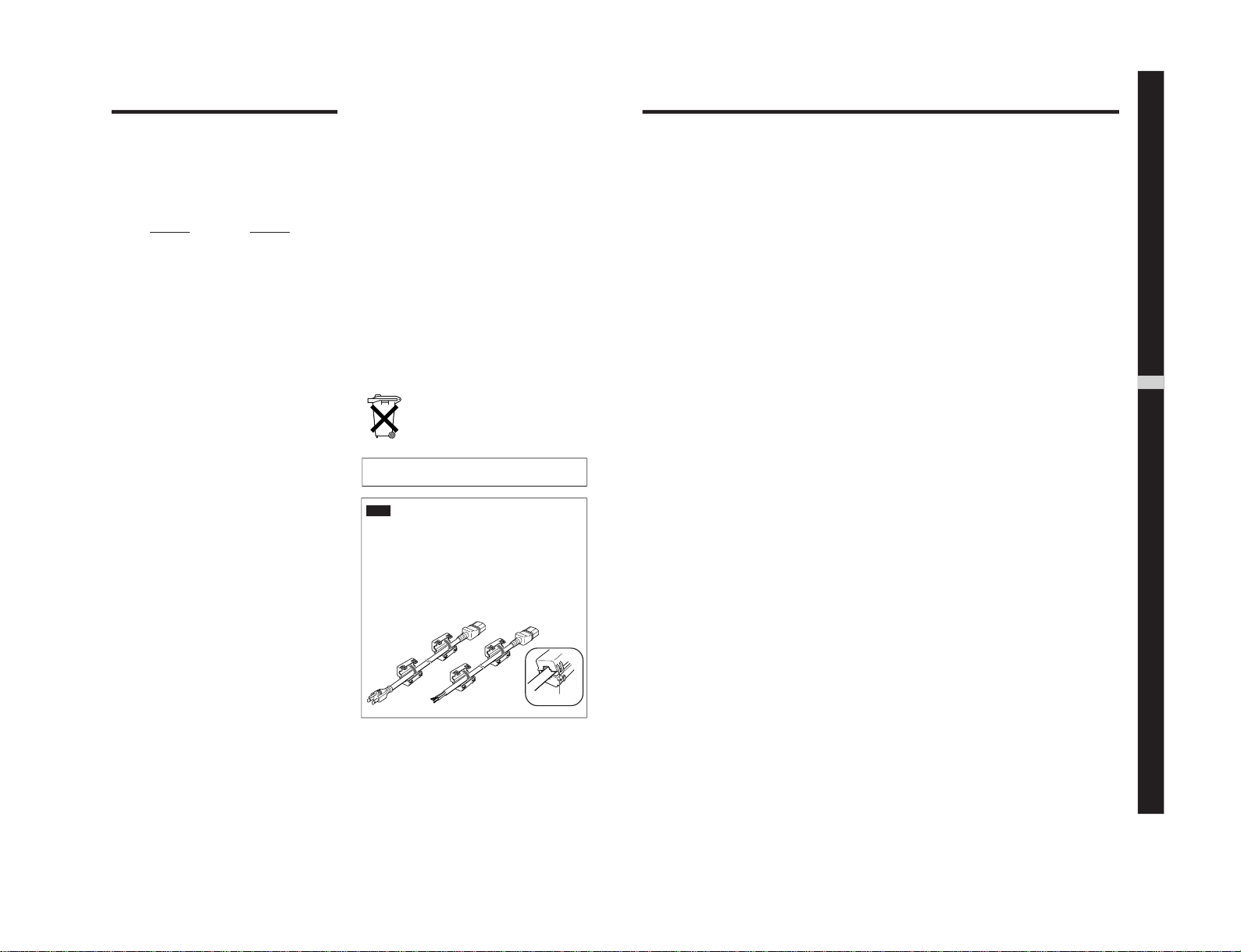
Note
When you connect a computer to this monitor,
attach the supplied ferrite cores. If you do not do
this, this monitor will not conform to mandatory
FCC/IC/CE (EN55022) standards.
Attaching the ferrite cores
Set the ferrite cores on the both ends of the AC
power cord. Close the lid tightly until the clamps
click.
3
(GB)
English
GB
Table of Contents
Precautions ............................................................... 5 (GB)
Features..................................................................... 6 (GB)
Location and Function of Parts and Controls ....... 7 (GB)
Front / Sides ............................................................. 7 (GB)
Control Panel ........................................................... 8 (GB)
Right Connector Panel ............................................. 9 (GB)
Left Connector Panel ............................................. 10 (GB)
Remote Commander RM-921................................ 11 (GB)
Installation............................................................... 13 (GB)
Using the Retractable Feet ..................................... 13 (GB)
Caution................................................................... 13 (GB)
Connections............................................................ 14 (GB)
Connecting the AC Power Cord ............................ 14 (GB)
Connection Example.............................................. 14 (GB)
Using On-screen Menus ........................................ 16 (GB)
Operating Through Menus..................................... 16 (GB)
Menu Guide ........................................................... 16 (GB)
Watching the Picture.............................................. 20 (GB)
Switching the Input Signal..................................... 20 (GB)
Switching the Display Mode.................................. 20 (GB)
Input Signal and Monitor Status Information
Display .............................................................. 21 (GB)
Adjusting the Picture ............................................. 23 (GB)
Adjusting the Contrast, Brightness, Chroma,
and Phase, etc.................................................... 23 (GB)
Restoring the PIC CONTROL Menu Items to Original
Settings ............................................................. 24 (GB)
Resizing and Positioning the Picture ................... 25 (GB)
Resizing the Picture ............................................... 25 (GB)
Adjusting the Picture Position ............................... 26 (GB)
Restoring the Original Picture Size and Position... 26 (GB)
Enlarging a 4:3 Image to a 16:9 Screen Naturally
(Wide Zoom Mode) .......................................... 27 (GB)
Adjusting the Pixels ............................................... 28 (GB)
Using the Memory Function .................................. 29 (GB)
Storing the Current Setting .................................... 29 (GB)
Calling Up a Stored Setting ................................... 30 (GB)
PFM-500A3WE/500A3WG/500A3WU/510A2WE/510A2WG/510A2WU
Page 11

PFM-500A3WE/500A3WG/500A3WU/510A2WE/510A2WG/510A2WU
4
(GB)
Selecting the On-screen Language ...................... 31 (GB)
Reducing Afterimage/Ghosting
(Screen Saver Function).................................... 31 (GB)
Reversing the Image .............................................. 31 (GB)
Changing the Display Position Automatically....... 33 (GB)
Controlling Power On/Off Automatically (Power
Control Function)............................................... 34 (GB)
Power Saving Function .......................................... 34 (GB)
On/Off Timer Function .......................................... 35 (GB)
Self-diagnosis Function......................................... 36 (GB)
Operating a Specific Monitor With the Remote
Commander ........................................................ 36 (GB)
Using Other Remote Commander Models ........... 38 (GB)
Specifications ......................................................... 39 (GB)
5
(GB)
Precautions
Precautions
On safety
•Operate the unit on 100 to 120 V AC or 220 to 240
V AC.
•A nameplate indicating operating voltage, power
consumption, etc. is located on the rear.
•Should any solid object or liquid fall into the cabinet,
unplug the unit and have it checked by qualified
personnel before operating it any further.
•Unplug the unit from the wall outlet if it is not to be
used for several days or more.
•To disconnect the AC power cord, pull it out by
grasping the plug. Never pull the cord itself.
•When the unit is installed on the floor, be sure to use
the retractable feet.
On installation
•Allow adequate air circulation to prevent internal
heat build-up. Do not place the unit on surfaces
(rugs, blankets, etc.) or near materials (curtains,
draperies) that may block the ventilation holes.
•Do not install the unit in a location near heat sources
such as radiators or air ducts, or in a place subject to
direct sunlight, excessive dust, mechanical vibration
or shock.
•When you install multiple equipment with the unit,
the following, such as malfunction of the Remote
Commander, noisy picture, noisy sound, may occur
depending on the position of the unit and other
equipment.
On the PDP (Plasma Display Panel)
•There may be some tiny black points and/or bright
points on the PDP. These points are normal.
•Do not display the same still image on the screen for
a long time. Otherwise, an afterimage or ghost may
appear on a part of the panel. Use the screen saver
function to equalize use of the screen display.
On cleaning
To keep the unit looking brand-new, periodically
clean it with a mild detergent solution. Never use
strong solvents such as thinner or benzine, or abrasive
cleansers since these will damage the cabinet. As a
safety precaution, unplug the unit before cleaning it.
On repacking
Do not throw away the carton and packing materials.
They make an ideal container in which to transport the
unit. When shipping the unit to another location,
repack it as illustrated on the carton.
If you have any questions about this unit, contact your
authorized Sony dealer.
For PFM-510A2WE/500A3WE Users
The PFM-510A2WE/500A3WE Flat Panel Monitor
will not function by itself.
Install the BKM-500 or BKM-501D Input Adaptor in
the monitor.
If you are using the BKM-500, refer to this Operating
Instructions.
If you are using the BKM-501D, refer to the
Operating Instructions supplied with the BKM-501D.
For more details, contact your authorized Sony dealer.
1-3
Page 12
1-4
6
(GB)
Features
Features
The PFM-510A2W/500A3W series are 16:9 42-inch
flat panel monitors adopting a PDP (Plasma Display
Panel), which can accept various types of signals with
the built-in scan converter.
Improved image quality
The PFM-510A2W series achieves higher image
quality with its PDP (Plasma Display Panel) set to
1024 dots × 1024 lines. This makes for a finelydetailed HDTV and PC image.
The PFM-500A3W series achieves brighter image
quality with 852 dots (horizontal) × 480 lines
(vertical) adopting PDP technology.
Internal high-performance scan converter
The monitor has a high performance scan converter.
Using a unique algorithm, the monitor processes
signals in a wide range of formats – Video, HDTV,
PC, etc.
Flexibility
An option slot is in place for future expansion.
The slot-in option adapter allows for quick and easy
system upgrades.
Other features
•Three sets of video inputs with audio inputs: one
composite video or Y/C input, one RGB input, and
one RGB/component input.
•Displays the HDTV signal with a tri-level sync
signal.
•Three dimensional comb filter for NTSC Y/C
separation.
•Line correlation comb filter for PAL Y/C separation.
•Automatic input signal detection with on-screen
indication.
•Windows
1)
95/98 PnP (Plug and Play) compatible.
•Picture AGC function — this function automatically
adjusts and improves the contrast when a low
intensity signal is input.
•On-screen menu for various adjustments and settings
•On-screen display in six languages for user-friendly
access. (Languages: English, German, French,
Italian, Spanish and Japanese)
•Fine adjustment of image size and position
•Memory function for storage of up to twenty picture
settings.
•ID control
•Self-diagnosis function.
•Remote (RS-232C) connector (mini DIN 8-pin)
•Control-S connector
•Accepts infrared or wired Sony Remote
Commanders using SIRCS code.
•Vertical setup
•Closed caption decoder
•Screen saver to reduce an afterimage or ghosting.
Warning on power connection
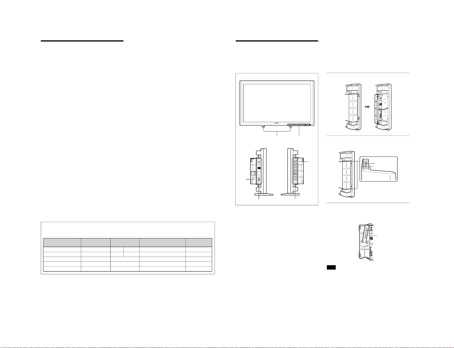
Use a proper power cord for your local power supply.
United States, Continental United Kingdom, Ireland, Japan
Canada Europe Australia, New Zealand
Plug type VM0033B COX-07 636 —
a)
VM1296
Female end VM0113 COX-02 VM0310B VM0303B VM1313
Cord type SJT H05VV-F CEE (13) 53rd (O.C) HVCTF
Minimum cord set rating 13A/125V 10A/250V 10A/250V 10A/125V
Safety approval UL/CSA VDE VDE DENTORI
1) Windows is a registered trademark of the Microsoft Corporation.
.........................................................................................................................................................................................................
a) Note: Use an appropriate rating plug which is applied to local regulations.
7
(GB)
Screws
Remote
Commander
Location and Function
of Parts and Controls
Front / Sides
1 Retractable feet
Use for setting the monitor on the floor.
For details on using the retractable feet, see “Using the
Retractable Feet” on page 13 (GB).
2 Control panel
For details on the control panel, see “Control Panel” on
page 8 (GB).
3 Left panel cover
Open this when using the left connector panel.
You can install the Remote Commander in a slot on
the back of this cover.
For details on opening the panel cover, see the right-hand
side of this page.
4 Left connector panel
For details on the left connector panel, see “Left Connector
Panel” on page 10 (GB).
5 Right connector panel
For details on the right connector panel, see “Right
Connector Panel” on page 9 (GB).
6 Right panel cover
Open this when using the right connector panel.
For details on opening the panel cover, see below.
To open the panel cover
Loosen the screws counterclockwise and open the cover.
To take off the panel cover
Loosen the screws as illustrated below and take off
the panel cover.
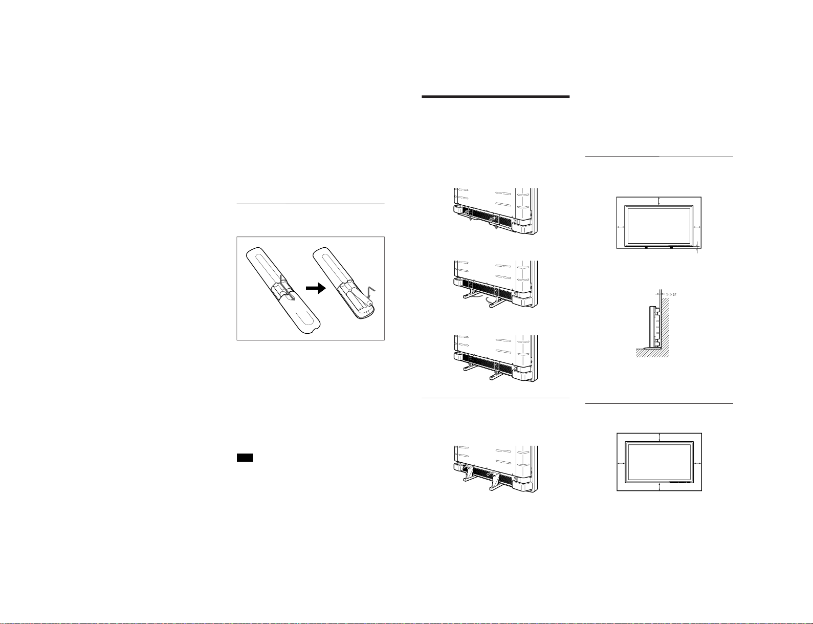
To install the Remote Commander in the
panel cover
Install the Remote Commander in the slot on the back
of the left panel cover as illustrated below.
Note
When housing the Remote Commander, make sure
that the top of the Remote Commander faces upward
and the rear faces outside.
Left side
Front
Right side
Location and Function of Parts and Controls
4
3
1
2
5
6
PFM-500A3WE/500A3WG/500A3WU/510A2WE/510A2WG/510A2WU
Page 13
PFM-500A3WE/500A3WG/500A3WU/510A2WE/510A2WG/510A2WU
8
(GB)
Control Panel
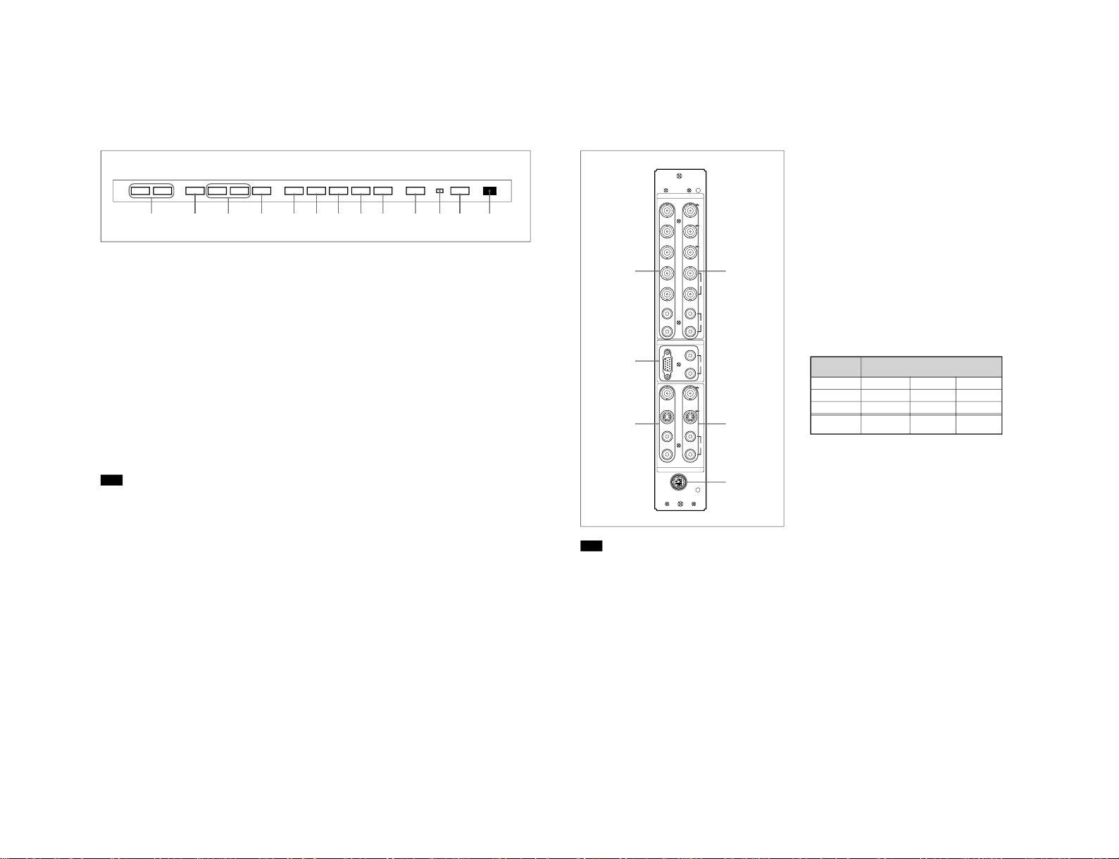
1 Remote control detector
Receives the beam from the Remote Commander.
2 1 (standby) switch/1 (standby) indicator
Press to turn on the monitor. Press again to go back to
the standby mode.
The 1 (standby) indicator lights up in red in the
standby mode.
When the 1 indicator flashes, see “Self-diagnosis
Function” on page 36 (GB).
3 Power indicator
Lights up when the monitor is turned on.
4 CTRL (control) button
To operate the buttons on the control panel, first press
this button. When the buttons light up or flash that
shows that they can be operated. Press again to
deactivate them.
Note
The buttons (except for 1 (standby) switch 2) on the
control panel do not function if you do not press the
CTRL button first.
5 Y/C button
Selects the signal input from the Y/C IN jack among
the LINE connectors.
6 LINE button
Selects the signal input from the VIDEO IN connector
among the LINE connectors.
7 RGB2 button
Selects the signal input from the RGB2 connectors.
8 YUV button
Selects the component signal input from the RGB1
connectors.
9 RGB1 button
Selects the RGB signal input from the RGB1
connectors.
0 ENT (enter) button
Press to select the desired item from the menu
displayed.
qa M/m buttons
Press to move the cursor (B) to an item or to adjust a
value in a menu.
qs MENU button
Press to make the menu appear.
qd VOL (volume) +/– buttons
Press the + button to increase the volume, or the –
button to decrease the volume.
Location and Function of Parts and Controls
VOL – VOL + MENU ENT RGB1 YUV RGB2 LINE Y/C CTRL
mM
1
qd qs qa 0 98765 4 32 1
9
(GB)
1 RGB1 IN connectors
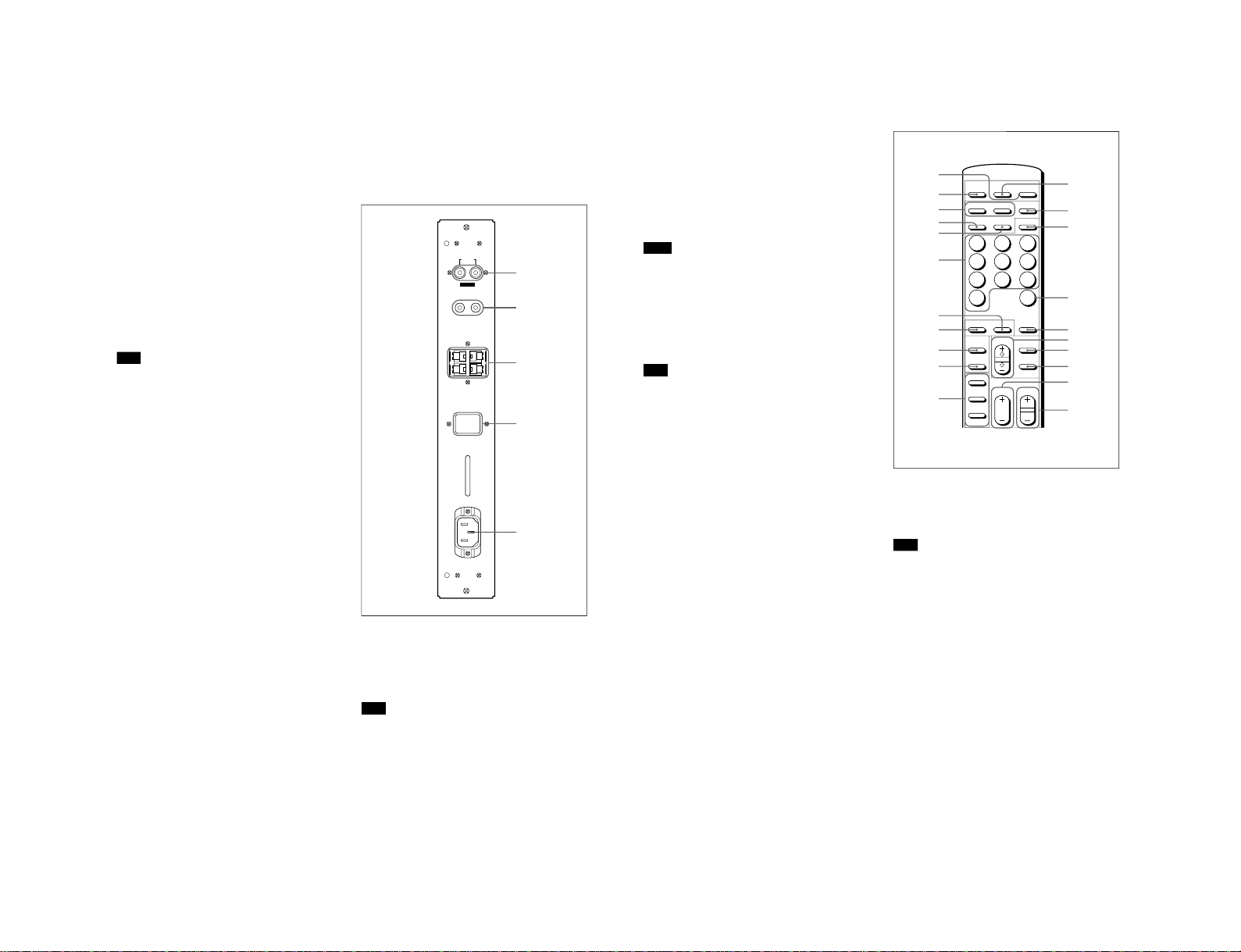
R (R-Y)/G (Y)/B (B-Y) IN (BNC-type): Inputs an
analog RGB signal or a component signal.
Connects to the RGB signal or component (Y/BY/R-Y) signal output of a computer or video
equipment.
This monitor also accepts an HD analog
component (Y/P
B/PR
) signal. Inputs the P
B
signal
to the B (B-Y) IN connector and P
R
signal to the
R (R-Y) IN connector.
HD/COMP IN (BNC-type): Inputs an H sync signal
or a composite sync signal. Connects to the H
sync signal or composite sync signal output of a
computer or video equipment.
VD IN (BNC-type): Inputs the V sync signal.
Connects to the V sync signal output of a
computer or a piece of video equipment.
An external sync signal is selected automatically.
See the priority chart below.
AUDIO IN (L/R) (phono type): Inputs an audio
signal. Connects to the audio output of a
computer or a piece of video equipment.
Connects to the channel L when the audio signal
is monaural.
2 RGB2 IN connectors
RGB IN (D-sub 15-pin): Connects to the RGB
signal output of a computer.
AUDIO IN (L/R) (phono type): Inputs an audio
signal. Connects to the audio output of a
computer. Connects to channel L when the audio
signal is monaural.
3 LINE IN connectors
VIDEO IN (BNC-type): Connects to the composite
video signal output of the video equipment.
Y/C IN (Mini DIN 4-pin): Connects to the Y/C
signal output of the video equipment.
AUDIO IN (L/R) (phono type): Connects to the
audio output of the video equipment. Connects to
channel L when the audio signal is monaural.
Input Input sync signals
connector
HD/COMP IN H Sync Comp Sync —
VD IN V Sync — —
G(Y) IN Sync on G Sync on G Sync on G
Sync signals
H Sync Comp Sync Sync on G
to be selected
V Sync
Right Connector Panel
Note
The image enhancing process for video signals
(NTSC, PAL, SECAM, NTSC4.43, PAL60) works
only for composite (Y/C) or component (Y/R-Y/B-Y)
input. The image from the RGB input may look
blurred. This is normal.
RGB IN
RGB 1
RGB 2
LINE
REMOTE
(RS-232C)
IN OUT
IN OUT
R
R-Y
G
Y
B
B-Y
HD/
COMP
VD
L
R
SYNC
AUDIO
Y/C
VIDEO
L
R
AUDIO
L
R
AUDIO IN
1
2
3
4
5
6
Location and Function of Parts and Controls
1-5
Page 14
1-6
10
(GB)
4 RGB1 OUT connectors
These connectors are used as loop-through outputs of
the RGB1 IN connectors 1.
When the plug is connected to the RGB OUT
connectors, the 75-ohms termination of the RGB IN
connectors is released, and the signal input to the
RGB IN connectors is output from the these
connectors.
R (R-Y)/G (Y)/B (B-Y) OUT (BNC-type): Loop-
through outputs of the RGB IN connectors.
Connects to the RGB signal or component (Y/BY/R-Y) signal input of another monitor.
HD/COMP OUT (BNC-type): Loop-through output
of the HD/COMP IN connector. Connects to the
H sync signal or composite sync signal input of
another monitor.
VD OUT (BNC-type): Loop-through output of the
VD IN connector. Connects to the V sync signal
input of another monitor.
Note
The HD/COMP OUT and VD OUT connectors are
high impedance outputs.
When using these outputs, connect a monitor with a
high impedance sync input connector, or the picture
might oscillate or disappear because of the sync
signal level mismatch.
AUDIO OUT (L/R) (phono type): Loop-through
outputs of the AUDIO IN jacks. Connects to the
audio inputs of another monitor.
5 LINE OUT connectors
These connectors are used as loop-through outputs of
the LINE IN connectors 3.
When the plug is connected to the VIDEO OUT
connector or Y/C OUT jack, the 75-ohms termination
of the VIDEO IN connector or Y/C IN jack is
released, and the signal input to the VIDEO IN or Y/C
IN jack is output from the VIDEO OUT connector or
Y/C OUT jack.
VIDEO OUT (BNC-type): Connects to the
composite video signal input of another monitor
or video equipment.
Y/C OUT (Mini DIN 4-pin): Connects to the Y/C
signal input of another monitor or a piece of
video equipment.
AUDIO OUT (L/R) (phono type): Loop-through
outputs of the AUDIO IN jacks. Connects to the
audio inputs of another monitor or a piece of
video equipment.
Location and Function of Parts and Controls
6 REMOTE (RS-232C) connector (mini DIN 8pin)
This connector allows remote control of the monitor
using the RS-232C protocol. For details, contact your
authorized Sony dealer.
Left Connector Panel
1 MONITOR OUT AUDIO (L/R) jacks (phono
type)
Outputs the signal input from the AUDIO IN jacks.
Connects to the audio inputs of an audio amplifier
(not supplied).
Note
These jacks are variable outputs. Set the volume to the
maximum position to set the output level to
500 mVrms.
MONITOR OUT
CONTROL S
SPEAKERS
(6-16 Ω)
AC IN
SERVICE CODE
AUDIO
RL
IN
+
R–
+
L
–
OUT
VARIABLE
5
4
3
2
1
8.8.
11
(GB)
2
5
8
ZOOM
DISPLAY
RGB2
Y/C
SELECT
VOL
3
6
9
CH
DEGAUSS
POWER
YUV
MTS/MPX
CH
1
4
7
10/0
STILL
MUTING
RGB1
LINE
MENU
ENTER
ON
OFF
ON
POWER
ID MODE
SET
OFF
qs
qd
qf
qg
qh
qj
qk
ql»
w;…
wa
1
2
3
4
5
6
7
8
9
0
qa
2 CONTROL S IN/OUT jacks (mini jacks)
Connects to the CONTROL S jacks of video
equipment or another monitor. Then you can
simultaneously control all equipment with a single
Remote Commander.
To control equipment by aiming the supplied Remote
Commander at the remote control detector of the
monitor, connect the CONTROL S OUT jack of the
monitor and the CONTROL S IN jack of the other
equipment.
Notes
•If you connect the CONTROL S IN jack to the other
equipment’s CONTROL S OUT jack, you cannot
operate the monitor with the Remote Commander.
•You can use a stereo cable with a mini plug instead
of the control S cable.
3 SPEAKERS L/R terminals
Connects to speakers with 6 to 16 ohms impedance.
Note
Do not connect the speaker’s cord to the monitor and
to an amplifier simultaneously, or an excessive
electric current might flow from the amplifier and
damage the monitor.
4 SERVICE CODE indicator
The indicator is only for qualified personnel.
5 -AC IN socket
Connect the supplied AC power cord to this socket
and to a wall outlet. Once you connect the AC power
cord, the 1 (standby) indicator lights up in red and
the monitor turns to standby mode.
Remote Commander RM-921
1 POWER switch
Press to turn on the monitor. Press again to go back to
the standby mode.
Note
When using multiple monitors, press this switch to
turn monitors which are already on to the standby
mode, or turn on monitors which are in the standby
mode.
2 MUTING button
Press to mute the sound. Press this button again or
press the VOL (volume) +/– button to obtain the
sound again.
3 RGB1/RGB2 buttons
Select the signal input from the RGB1 or RGB2
connectors.
4 LINE button
Selects the signal input from the VIDEO IN connector
in the LINE connectors.
Location and Function of Parts and Controls
PFM-500A3WE/500A3WG/500A3WU/510A2WE/510A2WG/510A2WU
Page 15
PFM-500A3WE/500A3WG/500A3WU/510A2WE/510A2WG/510A2WU
12
(GB)
5 Y/C button
Selects the signal input from the Y/C IN jack in the
LINE connectors.
6 Number buttons
Press to select the index number.
7 ZOOM button
Each time you press this button, the image size
changes (in order) to double (×2), triple (×3),
quadruple (×4) and original size.
8 STILL button
This button does not operate with the monitor.
9 POWER ON switch
Press to turn on the monitor. When you use multiple
monitors, you can use this switch instead of the
POWER switch 1 so as not to affect another monitor
which may be already turned on.
0 POWER OFF switch
Press to turn the monitor to the standby mode. When
you use multiple monitors, you can use this switch
instead of the POWER switch 1 so as not to affect
another monitor which may be in the standby mode.
qa ID MODE (ON/SET/OFF) buttons
Press the ON button to make an index number appear
on the screen. Then press the index number of the
monitor you want to operate and press the SET button.
After you finish the operation, press the OFF button to
return to the normal mode.
qs DISPLAY button
Displays the input signal information and the time at
the top of the monitor screen. Press again to clear it.
qd YUV button
Selects the component signal input from the RGB1
connectors.
qf MTS/MPX button
This button does not operate with the monitor.
qg CH button
This button does not operate with the monitor.
qh DEGAUSS button
This button does not operate with the monitor.
qj SELECT +M/–m buttons
Press to move the cursor (B) to an item or to adjust a
value in a menu.
Location and Function of Parts and Controls
qk MENU button
Press to make the menu appear.
ql ENTER button
Press to select the desired item in a menu.
w; VOL +/– buttons
Press the + button to increase the volume, or the –
button to decrease the volume.
wa CH +/– buttons
This button does not operate with the monitor.
Installing batteries
Insert two size AA (R6) batteries in correct polarity.
e
E
E
e
•In normal operation, batteries will last up to half a
year. If the Remote Commander does not operate
properly, the batteries might be exhausted sooner.
Replace them with new ones.
•To avoid damage from possible battery leakage,
remove the batteries if you do not plan to use the
Remote Commander for a fairly long time.
When the Remote Commander does not work
Check that the 1 indicator lights up. The Remote
Commander operates the monitor only when the
monitor is turned on, or it is in the standby mode.
Note
When you use multiple monitors, if you connect the
cable to the CONTROL S IN jack on the side of the
monitor, you cannot operate the monitor with the
Remote Commander.
Be sure to
install the
negative <
–
end first.
13
(GB)
Installation
Installation
Using the Retractable Feet
This section describes the installation arrangements
for installing the monitor.
1
Pull out the knobs and pull down the retractable
feet.
2
Turn the retractable feet outward.
3
Push in the retractable feet until you hear the
click.
To fix the retractable feet in place
When the monitor is installed on the floor, be sure to
fix the retractable feet in place.
Install the foot support brackets as illustrated below.
Caution
•When you install the monitor, make sure there is
more space than that shown in the figure below.
•The ambient temperature must be 0 °C to +35 °C
(32 °F to 95 °F).
When using the retractable feet
Front
20 (7 7/8)
Wall
Floor
Wall Wall
10
(4)
10
(4)
2.5 (1)
Side
5.5 (2 1/4)
Wall
Floor
Units: cm (inches)
When using the mounting bracket
Front
25 (9 7/8)
25 (9
7
/8)
10
(4)
10
(4)
Wall
Wall
Wall Wall
1-7
Page 16
1-8
14
(GB)
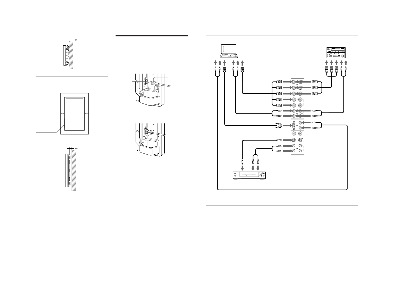
Make sure that
the control
section is at the
bottom.
5 (2)
Wall
Installation / Connections
Side
3.5 (1 7/16)
Wall
Units: cm (inches)
Hooked on the wall: Vertically
Front
10 (4)
10 (4)
25
(9 7/8)
20
(7 7/8)
Wall
WallWall
Wall
Side
Units: cm (inches)
Connections
Connecting the AC Power Cord
1
Plug the power cord into the AC IN socket. Then,
attach the AC plug holder (supplied) to the AC
power cord.
2
Slide the AC plug holder over the cord until it
connects to the AC IN socket cover.
To remove the AC power cord
Squeeze the upper and lower sides and pull out the
AC plug holder.
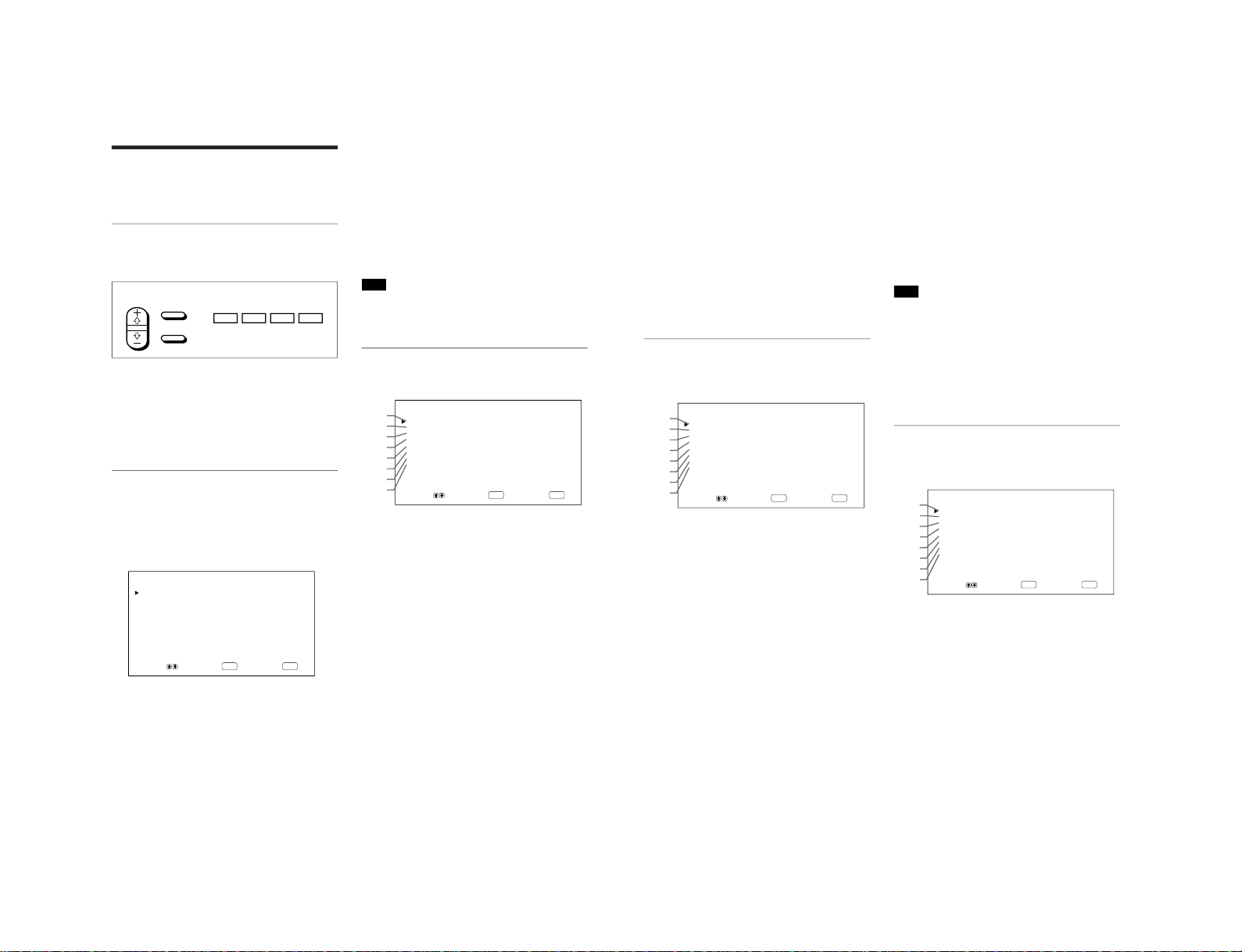
Connection Example
Before you start
•First make sure that the power to each piece of
equipment is turned off.
•Use connecting cables suitable for the equipment to
be connected.
•The cable connectors should be fully inserted into
the jacks. A loose connection may cause hum and
other noise.
•To disconnect the cable, pull it out by grasping the
plug. Never pull the cable itself.
•Read the instruction manual of the equipment to be
connected.
AC plug
holder
AC IN
socket
AC power
cord
AC IN
socket
cover
15
(GB)
Computer
to audio
output
to video
output
to video
output
to audio
output
to audio
output
to video
output
to AUDIO IN
to Y/C or
VIDEO IN
to AUDIO IN
to RGB IN
to AUDIO IN
to AUDIO IN
* to R(R-Y)/G(Y)/
B(B-Y), HD/COMP,
VD IN
* to R(R-Y)/G(Y)/
B(B-Y) IN
to audio
output
to component
signal output
Betacam SP video
cassette recorder
* cannot be used at the same time.
VCR, laser disc player, game
machine, etc.
Connections
RGB IN
RGB 1
RGB 2
LINE
IN OUT
IN OUT
R
R-Y
G
Y
B
B-Y
HD/
COMP
VD
L
R
SYNC
AUDIO
Y/C
VIDEO
L
R
AUDIO
L
R
AUDIO IN
PFM-500A3WE/500A3WG/500A3WU/510A2WE/510A2WG/510A2WU
Page 17
PFM-500A3WE/500A3WG/500A3WU/510A2WE/510A2WG/510A2WU
16
(GB)
Using On-screen Menus
Using On-screen Menus
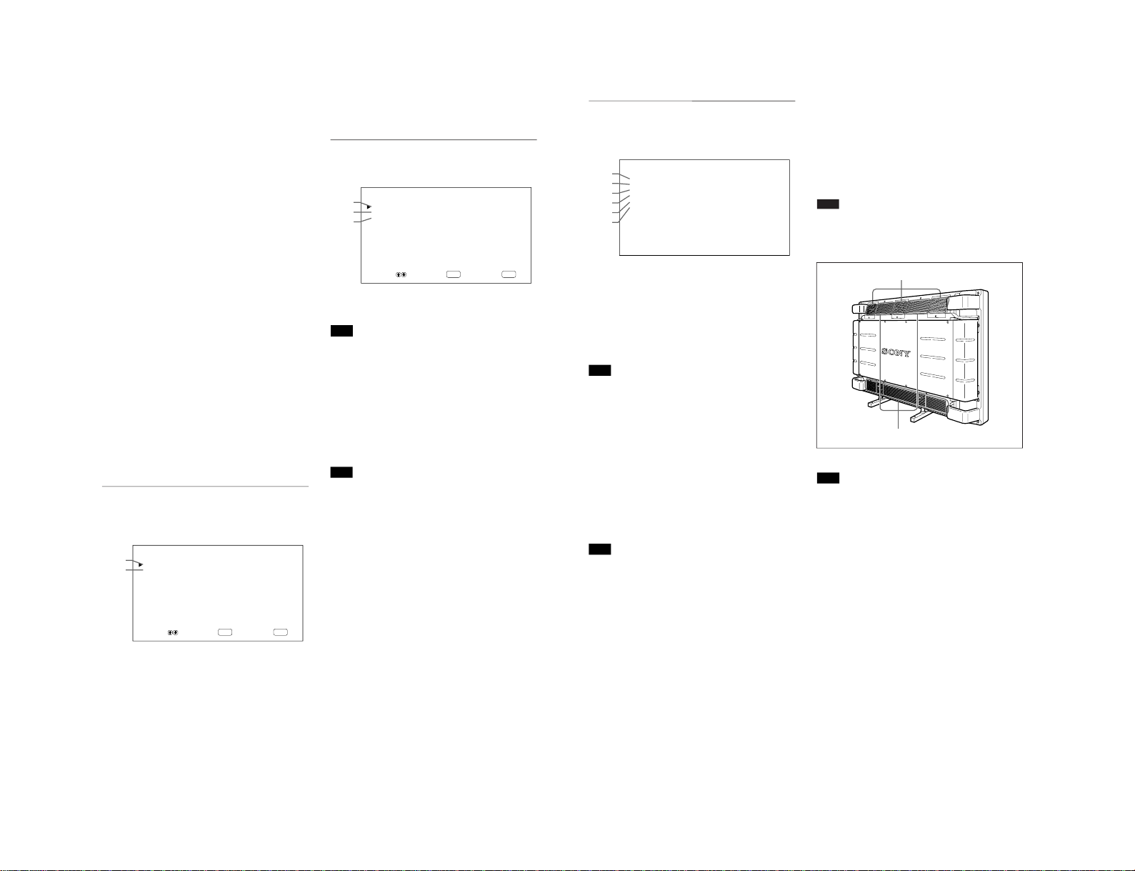
Operating Through Menus
Menu operating buttons
There are four buttons on the monitor and the Remote
Commander for menu operations.
SELECT
MENU
ENTER
MENU ENT
m
M
The buttons on the control panel are used for
explanation purposes in this operating instructions.
The ENTER button on the Remote Commander has
the same function as the ENT button on the control
panel and the SELECT +M/–m buttons on the Remote
Commander as same as the M/m buttons on the
control panel.
Configuration of the menu
To select the language used in the menu, see page
31 (GB).
1
Press MENU.
The main menu appears on the monitor screen.
ENTER
MENU
MA I N MENU
P I C CONT ROL
PIC SIZE
CONF I G
MEMORY
REMOTE
STATUS
SELECT SET END
2
Press M/m to move the cursor (B) and press ENT
to select a menu.
The selected menu appears on the monitor screen.
3
Press M/m to move the cursor (B) and press ENT
to select an item.
The menu for the selected item appears on the
monitor screen.
4
Press M/m to adjust or select the setting and press
ENT to set.
The setting is registered and the menu returns to
the previous menu.
To return to the normal screen, press the MENU
button repeatedly until the menu disappears.
Menu Guide
Note
“– – – –” appears next to an item when its function is
not available. The availability depends on the types of
input signal.
PIC CONTROL menu
This menu is used for adjusting the picture.
ENTER
MENU
P IC CONTROL
CONTRAST : 80
BRI GHTNESS : 00
CHROMA : 0 0
PHASE : 00
P ICTURE AGC : ON
COLOR TEMP : H I GH
SHARPNESS : MI D
4
3
2
1
5
6
7
8
RESET
SELECT SET END
1 CONTRAST
Press M to increase the contrast and press m to
decrease it.
2 BRIGHTNESS
Press M to make the picture brighter and press m to
make it darker.
3 CHROMA
Press M to increase color saturation and press m to
decrease it.
4 PHASE
Press M to make the overall picture greenish and press
m to make it purplish.
5 PICTURE AGC
Select ON to automatically increase the brightness
when a low brightness signal is input.
This function works only for LINE input or 15 kHz
YUV input.
Remote Commander Control Panel
17
(GB)
6 COLOR TEMP
Changes color temperature.
For details, see “COLOR TEMP” on page 23 (GB).
7 SHARPNESS
Changes the outline correction level in three levels
(HIGH, MID or LOW).
For details, see “SHARPNESS” on page 24 (GB).
8 RESET
Restores the factory settings in the PIC CONTROL
menu items 1 to 7.
For details on using the reset function, see “Restoring the
PIC CONTROL Menu Items to Original Settings” on page
24 (GB).
PIC SIZE menu
This menu is used for resizing and positioning the
picture.
ENTER
MENU
PIC SIZE
HSIZE : 00
HSHIFT : 00
VSIZE : 00
VSHIFT : 00
RESET
ASPECT : 4X3
ZOOM : X1
qs
qa
q;
9
qd
qf
qg
qh
PIXEL ADJUST
SELECT SET END
9 H SIZE
Adjusts the horizontal picture size. Press M to enlarge
the horizontal size and press m to diminish it.
q; H SHIFT
Adjusts the horizontal centering. Press M to move the
picture to the right and press m to move it to the left.
qa V SIZE
Adjusts the vertical picture size. Press M to enlarge
the vertical size and press m to diminish it.
qs V SHIFT
Adjusts the vertical centering. Press M to move the
picture up and press m to move it down.
qd RESET
Restores the factory settings in the PIC SIZE menu
items 9 to qs.
For details on using the reset function, see “Restoring the
Original Picture Size and Position” on page 26 (GB).
qf ASPECT
Sets the aspect ratio of the picture to 4:3, 16:9 or
wide-zoom size.
For details on the wide-zoom, see “Enlarging a 4:3 Image
to a 16:9 Screen Naturally (Wide Zoom Mode)” on page 27
(GB).
qg ZOOM
Enlarges the image (in order) to double (×2), triple
(×3) and quadruple (×4). You can also operate with
the ZOOM button on the Remote Commander.
Note
When you use the wide zoom mode, set ZOOM to ×1.
If ZOOM is set to ×2, ×3 or ×4, the wide zoom mode
cannot be used.
qh PIXEL ADJUST
Adjusts the dot phase and total number of horizontal
pixels when you see noise on the edges of the
characters and the vertical lines.
For details, see “Adjusting the Pixels” on page 28 (GB).
CONFIG menu
This menu is used for adjusting the signal or selecting
the language.
ENTER
MENU
CONF I G
DI SPLAY : ON
CLOSED CAPT ION: OFF
COLOR SYSTEM : AUTO
SCREEN F I L L : CENTER
POWER CONTROL
SCREEN SAVER
TIME SET
w;
ql
qk
qj
wa
ws
wd
wf
LA NGUAGE
SELECT SET END
qj DISPLAY
Selects ON to display the input signal information for
about five seconds at the top of the monitor screen
when turning on the power or switching the input
signal.
qk CLOSED CAPTION
Displays closed captions.
For details, see “Displaying Closed Captions” on page 20
(GB).
Using On-screen Menus
1-9
Page 18
1-10
18
(GB)
ql COLOR SYSTEM
Selects the input signal.
AUTO: to display NTSC, PAL or SECAM signals
443NT: to display NTSC4.43 signals
PAL60: to display PAL60 signals
w; SCREEN FILL
Selects the point of origin for resizing the picture.
CENTER: Sets the point of origin on the center of
the monitor.
CORNER: Sets the point of origin at the upper-left
corner of the monitor.
wa POWER CONTROL
Sets the length of time until the system goes into the
power saving mode.
For details, see “Controlling Power On/Off Automatically
(Power Control Function)” on page 34 (GB).
ws SCREEN SAVER
Enables the screen saver to reduce afterimage or
ghosting.
For details, see “Reducing Afterimage/Ghosting (Screen
Saver Function)” on page 31 (GB).
wd TIME SET
Sets the time.
For details, see “Adjusting the time” on page 21 (GB).
wf LANGUAGE
Selects the on-screen language (English, German,
French, Italian, Spanish or Japanese).
For details, see “Selecting the On-screen Language” on
page 31 (GB).
MEMORY menu
This menu is used for saving or recalling the settings
in the PIC CONTROL and PIC SIZE menus.
ENTER
MENU
MEMORY
LOAD
SAVE
wh
wg
SELECT SET END
For details, see “Using the Memory Function” on page 29
(GB).
wg LOAD
Recalls the preset settings.
wh SAVE
Saves the settings.
REMOTE menu
This menu is used for remote control settings.
ENTER
MENU
REMOTE
INDEX No. : 001
REMOTE MODE : TV
REMOTE ONLY : OFF
wk
wj
wl
SELECT SET END
wj INDEX No.
Sets the index number of the monitor.
Note
When you set the number, use the buttons on the
monitor.
For details about the index number, see “Operating a
Specific Monitor With the Remote Commander” on page 36
(GB).
wk REMOTE MODE
Selects the Remote Commander mode.
TV: The Sony monitors’ or the TVs’ commander
PJ: The Sony projectors’ commander
OFF: Disables the remote control.
Note
When you change the Remote Commander mode, use
the buttons on the monitor. You cannot change the
Remote Commander mode with the Remote
Commander.
For details, see “Using Other Remote Commander
Models” on page 38 (GB).
wl REMOTE ONLY
Select ON to disable the front control buttons on the
monitor. The monitor can only be controlled with the
Remote Commander. While REMOTE ONLY is ON,
the indicators on the front panel go off.
To cancel the REMOTE ONLY mode, set REMOTE
ONLY to OFF with the Remote Commander, or press
the CTRL button while pressing the 1 switch on the
monitor. The monitor turns to the standby mode and
the REMOTE ONLY mode is cancelled.
The setting in this item is still retained when the AC
power cord is disconnected or when you turn on/off
the monitor with the Remote Commander.
Using On-screen Menus
19
(GB)
STATUS menu
This menu is used for displaying the internal condition
of the monitor.
STATUS
MODEL NAME : P FM - 5 1 0A 2WU
SERIAL No . : 2800001
OPERATION : 000001H
SOFTWARE :
Ver
1.00
TEMPERATURE : OK
FAN : OK
ed
es
ea
e;
ef
eg
e; MODEL NAME
Indicates the model name.
ea SERIAL No.
Indicates the serial number.
es OPERATION
Indicates the total operation hours.
Note
The standby mode is not counted as part of the
OPERATION time.
ed SOFTWARE
Indicates the system software version.
ef TEMPERATURE
Indicates whether the internal temperature of the
monitor is normal.
OK: Normal
NG: Unusual
When the internal temperature is unusual, NG is
displayed and the item flashes in red. The 1 indicator
on the control panel also flashes.
Note
The “TEMPERATURE NG” message may appear
when the ventilation holes are blocked or the monitor
is installed in a poorly ventilated area. In this case,
check that the ventilation holes are not blocked and
install the monitor in a well ventilated area. If the
message is still displayed, contact your authorized
Sony dealer.
When the 1 indicator flashes or NG is indicated, see “Selfdiagnosis Function” on page 36 (GB).
Cooling fans
Ventilation holes
Using On-screen Menus
eg FAN
The cooling fans are built into this monitor. This item
indicates whether the cooling fans work properly.
OK: Normal
NG: Unusual
When the cooling fans are not working normally, NG
is displayed and the item flashes in red. The 1
indicator on the control panel also flashes.
Note
When the “FAN NG” message appears, contact your
authorized Sony dealer.
When the 1 indicator flashes or NG is indicated, see “Selfdiagnosis Function” on page 36 (GB).
Note
The upper cooling fans detect the monitor’s internal
temperature and control the fan rotation. If the
ambient temperature is high, the fan speed increases
and the noise will be louder.
PFM-500A3WE/500A3WG/500A3WU/510A2WE/510A2WG/510A2WU
Page 19
PFM-500A3WE/500A3WG/500A3WU/510A2WE/510A2WG/510A2WU
20
(GB)
Watching the Picture
Before you start
•Turn on the monitor.
•Turn on the connected equipment and play a video
source.
•To display the input signal information on the screen
when turning on the power or switching the input
signal, set “DISPLAY” in the CONFIG menu to ON.
•To select the on-screen language used in the menu,
see page 31 (GB).
Switching the Input Signal
1
Press CTRL on the control panel of the monitor.
The RGB1, YUV, RGB2, LINE, and Y/C buttons
light up.
2
Select the input source to be displayed by pressing
the following buttons.
RGB1:Selects the audio and video signal input
from the RGB1 connectors when the input
signal is an RGB signal.
YUV: Selects the audio and video signal input
from the RGB1 connectors when the input
signal is a component signal.
RGB2:Selects the audio and video signal input
from the RGB2 connectors.
LINE: Selects the audio and video signal input
from the VIDEO IN connector and
AUDIO IN jack among the LINE
connectors.
Y/C: Selects the audio and video signal input
from the Y/C IN connector and AUDIO
IN jack among the LINE connectors.
PAL
LINE Y/C
The selected input signal appears on the monitor
screen.
You can also switch the input signal with the
Remote Commander.
Watching the Picture
Note
We recommend input source video equipment
equipped with a TBC (time base corrector). If the
monitor receive a signal without TBC, the picture may
disappear due to disturbance of the sync signal.
Switching the Display Mode
Displaying Closed Captions
1
Press MENU.
The main menu appears on the monitor screen.
ENTER
MENU
MA I N MENU
P I C CONT ROL
PIC SIZE
CONF I G
MEMORY
REMOTE
STATUS
SELECT SET END
2
Press M/m to move the cursor (B) to “CONFIG”
and press ENT.
The CONFIG menu appears on the monitor
screen.
ENTER
MENU
CONF I G
DI SPLAY : ON
CLOSED CAPT ION: OFF
COLOR SYSTEM : AUTO
SCREEN F I L L : CENTER
POWER CONTROL
SCREEN SAVER
TIME SET
LA NGUAGE
SELECT SET END
3
Press M/m to move the cursor (B) to “CLOSED
CAPTION” and press ENT.
The following menu appears on the monitor
screen.
CLOSED CAPT ION: OFF
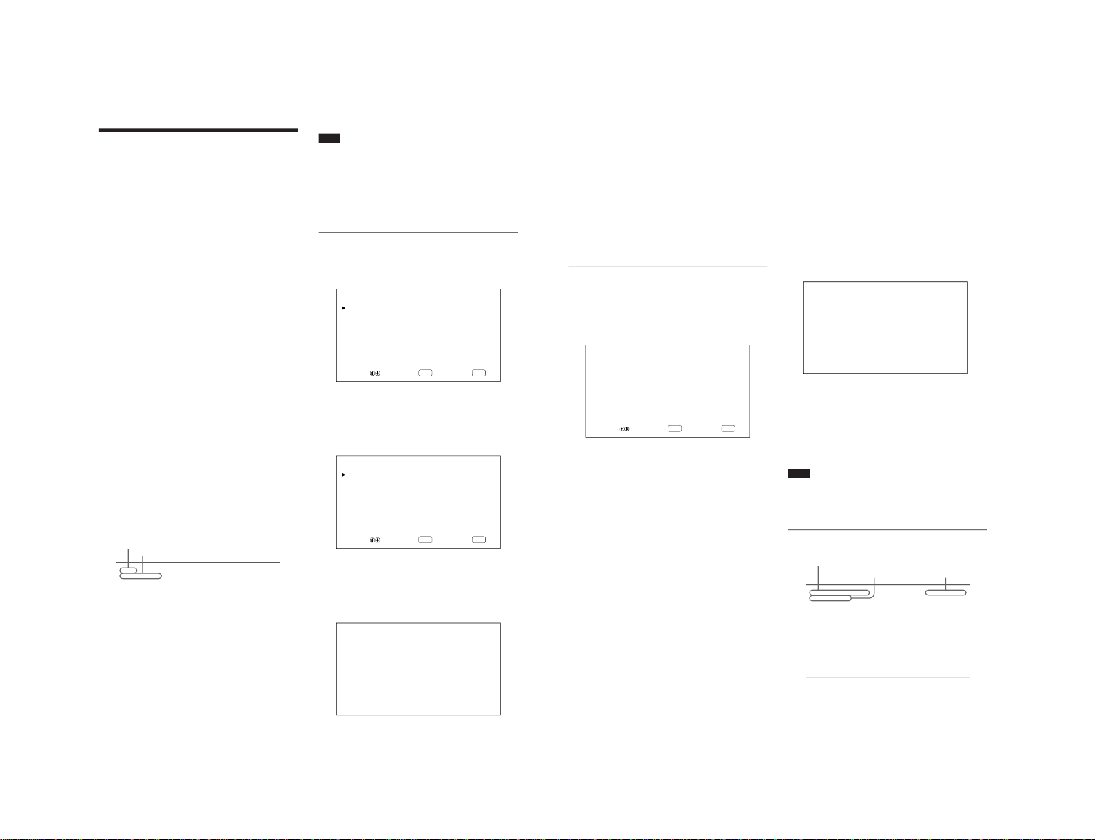
Color system or horizontal/vertical frequency
Signal type
21
(GB)
Input Signal and Monitor Status
Information Display
Input signal and monitor status information is
displayed on the monitor screen for about five seconds
when turning on the power or switching the input
signal.
To disable this function, follow the steps below.
1
In the CONFIG menu, press M/m to move the
cursor (B) to “DISPLAY” and press ENT.
The following menu appears on the monitor
screen.
DI SPLAY : ON
2
Press M/m to set DISPLAY to OFF and press
ENT.
The DISPLAY function is disabled.
To activate the information function, set DISPLAY to
ON in step 2 above. The factory default is ON.
Note
You can display the input signal information and the
time anytime by pressing the DISPLAY button on the
Remote Commander, regardless of the above setting.
The input signal information list
31.5kHz/60Hz 16:30:40
RGB1 RGB
Watching the Picture
4
Select the caption type.
OFF: The caption is not displayed.
CAPT1: Displays caption1 over the picture.
CAPT2: Displays caption2 over the picture.
TEXT1: Displays caption1 against a black
background.
TEXT2: Displays caption2 against a black
background.
5
Press MENU.
The menu returns to the CONFIG menu.
Adjusting the time
1
In the CONFIG menu, press M/m to move the
cursor (B) to “TIME SET” and press ENT.
The following menu appears on the monitor
screen.
ENTER
MENU
TIME SET : 00:00:00
SELECT SET END
2
Press ENT.
The background of the hour is displayed in cyan.
3
Adjust the hour with M/m and press ENT.
The hour is defined and the background of the
minute is displayed in cyan.
4
Similarly, adjust the minute and press ENT.
The minute is defined and the second is reset to
00.
To display the time, press the DISPLAY button on the
Remote Commander. The time is displayed in the
upper-right corner of the monitor.
Color system or horizontal/vertical frequency
Signal type
Time
1-11
Page 20
1-12
22
(GB)
Actual on-screen display of the monitor status
On-screen display Significance
31.5kHz / 60Hz (eg.) The selected input signal is
computer RGB.
525 / 60 (eg.) The selected input signal is RGB or
component video.
NTSC (eg.) The selected input signal is NTSC.
OTHERS The input signal is out of the
capture range.
NO SYNC There is no input signal.
MUTING The sound is muted.
RGB1 RGB The signal mode of RGB1 is set to
RGB.
RGB1 YUV The signal mode of RGB1 is set to
component video.
LINE COMPOSITE Composite video input is selected at
LINE.
LINE Y/C Y/C video input is selected at LINE.
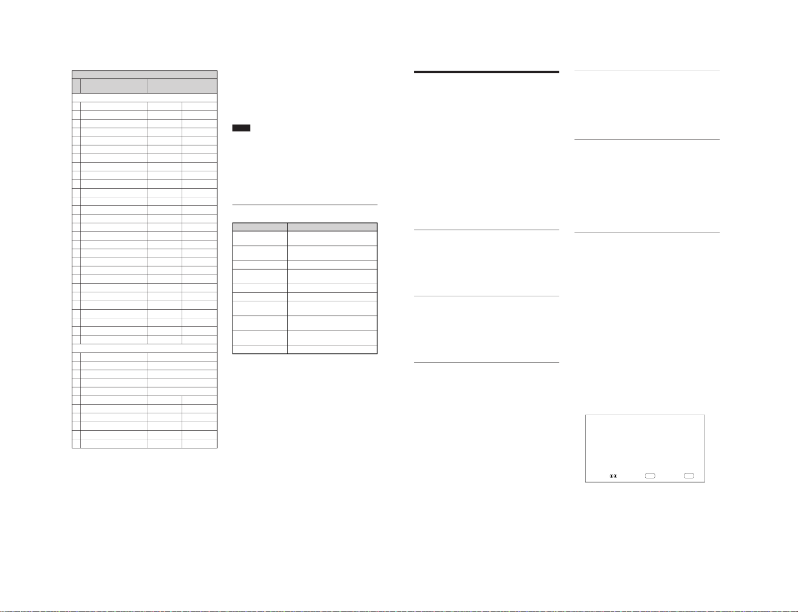
Preset input signals
Signal name
Color system or horizontal/
vertical frequency
Computer signals
1 VGAa)-1 (VGA 350) 31.5kHz 70Hz
2
640×350@85Hz (VESAb) STD)
37.9kHz 85Hz
3 640×400@85Hz (VESA STD) 37.9kHz 85Hz
4 640×480@60Hz (VESA STD) 31.5kHz 60Hz
5 Mac
c)
13
"
35.0kHz 67Hz
6 640×480@72Hz (VESA STD) 37.9kHz 73Hz
7 640×480@75Hz (VESA STD) 37.5kHz 75Hz
8 640×480@85Hz (VESA STD) 43.3kHz 85Hz
9 VGA (VGA TEXT) 31.5kHz 70Hz
10 720×400@85Hz (VESA STD) 37.9kHz 85Hz
11 800×600@56Hz (VESA STD) 35.2kHz 56Hz
12 800×600@60Hz (VESA STD) 37.9kHz 60Hz
13 800×600@72Hz (VESA STD) 48.1kHz 72Hz
14 800×600@75Hz (VESA STD) 46.9kHz 75Hz
15 800×600@85Hz (VESA STD) 53.7kHz 85Hz
16 Mac 16
"
49.7kHz 75Hz
17 1024×768@60Hz (VESA STD) 48.4kHz 60Hz
18 1024×768@70Hz (VESA STD) 56.5kHz 70Hz
19 1024×768@75Hz (VESA STD) 60.0kHz 75Hz
20 1024×768@85Hz (VESA STD) 68.7kHz 85Hz
21 1152×864@75Hz (VESA STD) 67.5kHz 75Hz
22 Mac 21
"
68.7kHz 75Hz
23 1280×960@60Hz (VESA STD) 60.0kHz 60Hz
24 1280×960@85Hz (VESA STD) 85.9kHz 85Hz
25
1280×1024@60Hz (VESA STD)
64.0kHz 60Hz
26
1280×1024@75Hz (VESA STD)
80.0kHz 75Hz
27
1280×1024@85Hz (VESA STD)
91.1kHz 85Hz
28
1600×1200@60Hz (VESA STD)
75.0kHz 60Hz
SDTV/HDTV
1 PAL PAL
2 NTSC NTSC
3 SECAM SECAM
4 NTSC4.43 NTSC/4.43
5 PAL60 PAL/60
6 1080/24psf 27.0kHz 48Hz
7 1080/50i 28.1kHz 50Hz
8 575/50p 31.3kHz 50Hz
9 480/60p 31.5kHz 60Hz
10 1080/60i 33.8kHz 60Hz
11 720/60p 45.0kHz 60Hz
Watching the Picture
a) VGA is a registered trademark of International Business
Machines Corporation, USA.
b) VESA is a registered trademark of the Video Electronics
Standards Association.
c) Mac (Macintosh) is a registered trademark of Apple
Computer, Inc.
Notes
•When inputting an HDTV signal, input the tri-level
sync signal to the G (Y) IN connector.
•When inputting the computer signal shown in item
No. 28, set the H SIZE, H SHIFT, V SIZE and V
SHIFT to the standard (00) and set ZOOM to ×1 in
the PIC SIZE menu, or the picture might oscillate.
23
(GB)
Adjusting the Picture
While watching the picture, you can adjust contrast,
brightness, chroma, phase, and so on, to suit your
taste. The adjustments can be carried out for each
input signal separately. You can also store the
adjusted levels in memory.
Adjusting the Contrast, Brightness,
Chroma, and Phase, etc.
Press MENU so that the main menu appears on the
monitor screen and select “CONTRAST”,
“BRIGHTNESS”, “CHROMA”, “PHASE”,
“PICTURE AGC”, “COLOR TEMP” or
“SHARPNESS” from the PIC CONTROL menu with
M/m.
CONTRAST
Select “CONTRAST” with M/m and press ENT.
Adjust the contrast with M/m in the range from MIN
(0) to MAX (+100).
M: to increase picture contrast
m: to decrease picture contrast
BRIGHTNESS
Select “BRIGHTNESS” with M/m and press ENT.
Adjust the brightness with M/m in the range from
MIN (–50) to MAX (+50).
M: to make the picture brighter
m: to make the picture darker
CHROMA
Select “CHROMA” with M/m and press ENT.
Adjust the chroma with M/m in the range from MIN
(–50) to MAX (+50).
M: to increase color intensity
m: to decrease color intensity
PHASE
Select “PHASE” with M/m and press ENT.
Adjust the phase with M/m in the range from MIN (–
50) to MAX (+50).
M: to make overall picture greenish
m: to make overall picture purplish
Automatic Brightness Control –
Enhancing the Image Contrast
If the average brightness of the image is low, the
system can automatically raise the contrast level to
enhance the brightness. This function works well for
displaying dark images.
Select “PICTURE AGC” with M/m and press ENT.
Set PICTURE AGC to ON or OFF with M/m.
COLOR TEMP (Color Temperature)
Set the color temperature. You can select HIGH or
LOW, or adjust each gain more precisely. Up to six
adjusted color temperatures can be registered. You
can rename them (up to six characters in length).
1
Select “COLOR TEMP” with
M/m
and press
ENT.
2
Select the color temperature with
M/m
and press
ENT.
HIGH: to set the color temperature to high
LOW: to set the color temperature to low
1 – 6: to set the gain more precisely
When you select HIGH or LOW, the menu returns
to the PIC CONTROL menu.
When you select “1” to “6”
When you select “1” to “6”, the following menu
appears on the monitor screen.
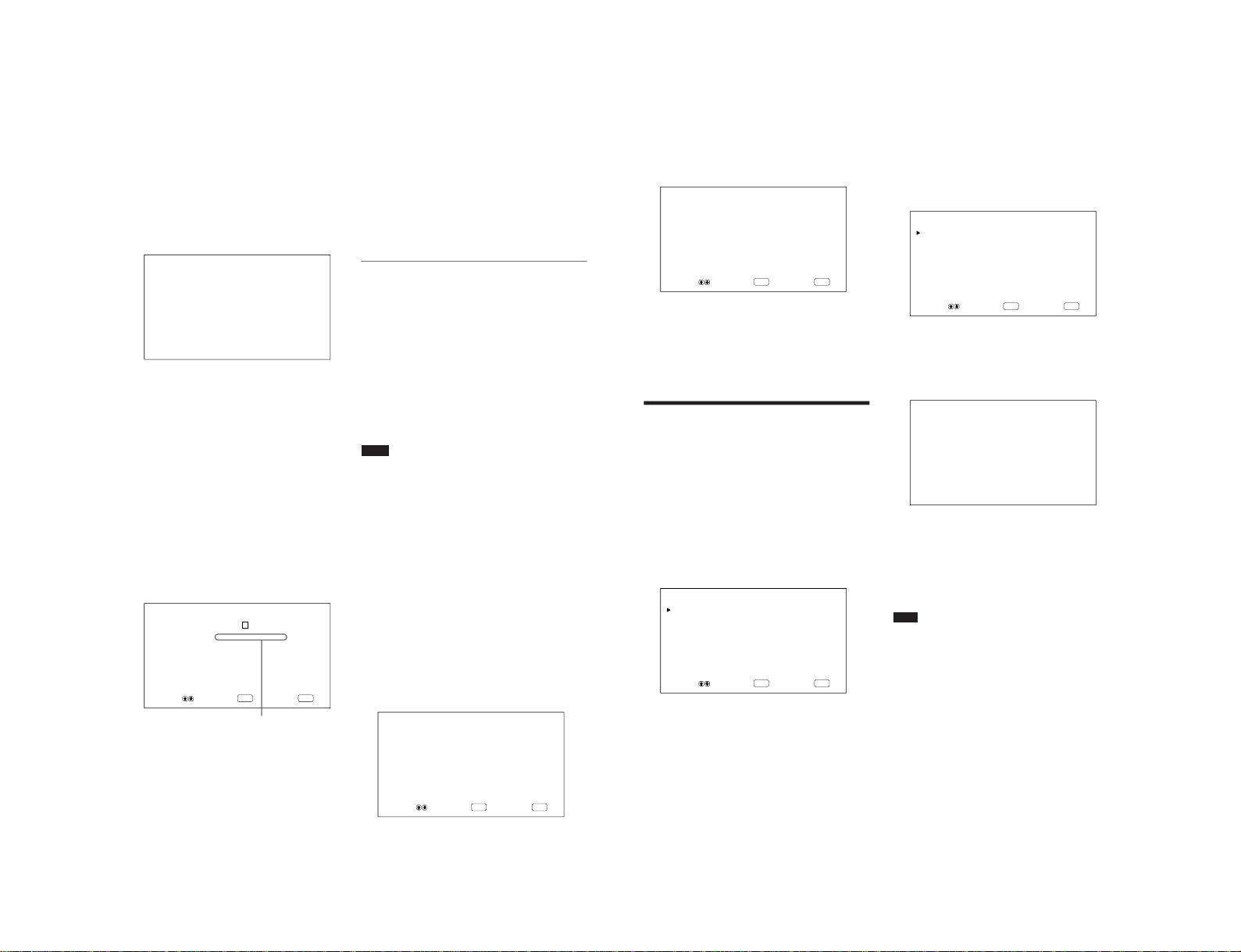
ENTER
MENU
COLOR TEMP : 1
RED GA I N : 2 55
GREEN GAIN : 255
BLUE GAI N : 255
NAME SE T
SELECT ADJUST END
Adjusting the Picture
PFM-500A3WE/500A3WG/500A3WU/510A2WE/510A2WG/510A2WU
Page 21
PFM-500A3WE/500A3WG/500A3WU/510A2WE/510A2WG/510A2WU
24
(GB)
(1) Select a number to register with
M/m
and
press ENT.
The cursor (B) appears on the monitor screen.
(2) Press M/m to move the cursor (B) to the gain
that you want to set.
The following menu appears on the monitor
screen.
COLOR TEMP : 1
RED GA I N : 2 55
(3) Adjust the gain (10 to 255) with M/m and
press MENU.
The menu returns to the COLOR TEMP
menu.
(4) Repeat steps (2) and (3) to set the other gains
and press MENU.
The menu returns to the COLOR TEMP
menu.
When you rename the adjusted color temperature,
follow the steps below.
(5) Press M/m to move the cursor (B) to “NAME
SET” and press ENT.
The following menu appears on the monitor
screen.
ENTER
MENU
COLOR TEMP : [ 1 ]
NAME SE T : [ – × ⁄=± 01234]
SELECT SET END
(6) Select the character to be changed with M/m
and press ENT.
The background of one character in the
character list changes to cyan.
(7) Select a character in the character list with
M/m and press ENT.
The selected character is input.
(8) Repeat steps (6) and (7) until you finish
inputting the name, then press MENU.
The menu returns to the COLOR TEMP
menu.
SHARPNESS
Change the outline correction level in three levels
(HIGH, MID or LOW).
1
Press
M/m
to move the cursor (B) to
“SHARPNESS” and press ENT.
2
Select the outline correction level with
M/m
and
press ENT.
HIGH: sharper picture
MID: standard value
LOW: softer picture
Notes
•CHROMA and PHASE controls do not function with
an RGB signal.
•PHASE control does not function with a component
signal.
•PHASE control does not function with a PAL or
SECAM color source.
•Do not change the CHROMA/PHASE (NTSC only)
level when the selected signal is black-and-white.
Although it has no effect on the current picture, it
does affect the picture of color signals such as NTSC
or PAL which may be input later.
Restoring the PIC CONTROL Menu
Items to Original Settings
1
In the PIC CONTROL menu, Press M/m to move
the cursor (B) to “RESET” and press ENT.
The following menu appears on the monitor
screen.
ENTER
MENU
RESET : NO
SELECT SET END
Character list
Adjusting the Picture
25
(GB)
2
Press M/m.
“NO” changes to “YES”.
ENTER
MENU
RESET : YES
SELECT SET END
3
Press ENT.
The PIC CONTROL menu items are restored.
To cancel the reset function, press MENU before
pressing ENT.
Resizing and Positioning
the Picture
You can shift the position of the picture so that it fits
the screen, or adjust the vertical and horizontal size of
the picture separately. You can adjust the setting to
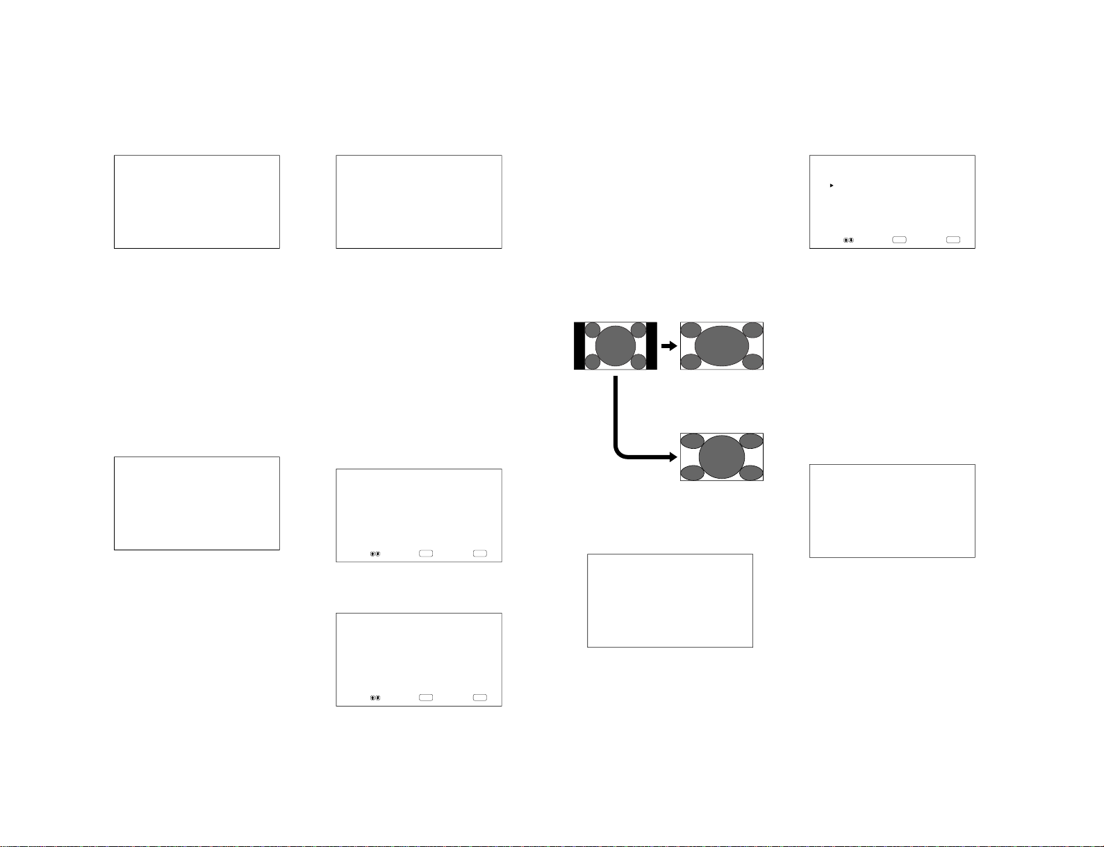
display the 4:3 image at the more natural 16:9 setting.
Resizing the Picture
1
Press MENU.
The main menu appears on the monitor screen.
ENTER
MENU
MA I N MENU
P I C CONT ROL
PIC SIZE
CONF I G
MEMORY
REMOTE
STATUS
SELECT SET END
2
Press M/m to move the cursor (B) to “PIC SIZE”
and press ENT.
The PIC SIZE menu appears on the monitor
screen.
ENTER
MENU
PIC SIZE
HSIZE : 00
HSHIFT : 00
VSIZE : 00
VSHIFT : 00
RESET
ASPECT : 4X3
ZOOM : X1
PIXEL ADJUST
SELECT SET END
3
Press M/m to move the cursor (B) to “H SIZE”
and press ENT.
The following menu appears on the monitor
screen.
HSIZE : 00
4
Press M/m to resize the picture.
M: to expand horizontal size
m: to reduce horizontal size
The horizontal picture size is indicated on the
monitor screen in the range from MIN (–50) to
MAX (+50). The factory preset value is 00.
Note
The lower limit of the setting may be above the MIN
depending on the input signal type.
5
Press ENT.
The menu returns to the PIC SIZE menu.
Adjusting the Picture / Resizing and Positioning the Picture
1-13
Page 22
1-14
26
(GB)
6
Press M/m to move the cursor (B) to “V SIZE”
and press ENT.
The following menu appears on the monitor
screen.
VSIZE : 00
7
Press M/m to resize the picture.
M: to expand vertical size
m: to reduce vertical size
The vertical picture size is indicated on the
monitor screen from MIN (–50) to MAX (+50).
The factory preset value is 00.
8
Press ENT.
The menu returns to the PIC SIZE menu.
Adjusting the Picture Position
1
In the PIC SIZE menu, press M/m to move the
cursor (B) to “H SHIFT” and press ENT.
The following menu appears on the monitor
screen.
HSHIFT : 00
2
Press M/m to shift the picture.
M: to shift the picture to the right
m: to shift the picture to the left
The horizontal picture position is indicated on the
monitor screen from MIN (–50) to MAX (+50).
The factory preset value is 00.
3
Press ENT.
The menu returns to the PIC SIZE menu.
4
Press M/m to move the cursor (B) to “V SHIFT”
and press ENT.
The following menu appears on the monitor
screen.
VSHIFT : 00
5
Press M/m to shift the picture.
M: to shift the picture upward
m: to shift the picture downward
The vertical picture position is indicated on the
monitor screen from MIN (–50) to MAX (+50).
The factory preset value is 00.
6
Press ENT.
The menu returns to the PIC SIZE menu.
Restoring the Original Picture Size
and Position
1
In the PIC SIZE menu, press M/m to move the
cursor (B) to “RESET” and press ENT.
The following menu appears on the monitor
screen.
ENTER
MENU
RESET : NO
SELECT SET END
2
Press M/m.
“NO” changes to “YES”.
ENTER
MENU
RESET : YES
SELECT SET END
Resizing and Positioning the Picture
27
(GB)
3
Press ENT.
The original picture size and position are restored.
To cancel the reset function, press MENU before
pressing ENT.
Enlarging a 4:3 Image to a 16:9
Screen Naturally (Wide Zoom Mode)
When you ordinarily watch a 4:3 standard image in
the 16:9 screen, the image is seen distorted in a
horizontal direction due to the difference in
proportion. If you use wide zoom mode, the center of
the monitor will not be distorted as much and the
corners of the monitor will be distorted instead. You
can change the linearities by adjusting the H
LINEARITY and V LINEARITY settings.
1
In the PIC SIZE menu, press M/m to move the
cursor (B) to “ASPECT” and press ENT.
The following menu appears on the monitor
screen.
ASPECT : 4X3
2
Press M/m to move the cursor (B) to “W ZOOM”
and press ENT.
The following menu appears on the monitor
screen.
ENTER
MENU
ASPECT :W ZOOM
H LINEARITY : 00
V LINEARITY : 00
RESET
SELECT SET END
3
If you do not change H LINEARITY or V
LINEARITY, press ENT.
The menu returns to the PIC SIZE menu.
When you change H LINEARITY or V
LINEARITY, follow the steps below.
4
Press M/m to move the cursor (B) to “H
LINEARITY” or “V LINEARITY” and press
ENT.
H LINEARITY: to change the linearity in the
horizontal direction
V LINEARITY: to change the linearity in the
vertical direction
The following menu appears on the monitor
screen. (The illustration below is for selecting the
H LINEARITY.)
ASPECT :W ZOOM
H LINEARITY : 00
5
Adjust the screen size with M/m.
To restore wide zoom mode items to their
original settings
In the ASPECT menu, select W ZOOM and press
ENT. Press M/m to move the cursor (B) to “RESET”
and press ENT. Then select YES with M/m and press
ENT.
The 4:3 standard image
The 4:3 image after setting
ASPECT to W ZOOM and
both linearities to standard
(00)
The 4:3 image after setting
ASPECT to 16×9
Resizing and Positioning the Picture
PFM-500A3WE/500A3WG/500A3WU/510A2WE/510A2WG/510A2WU
Page 23
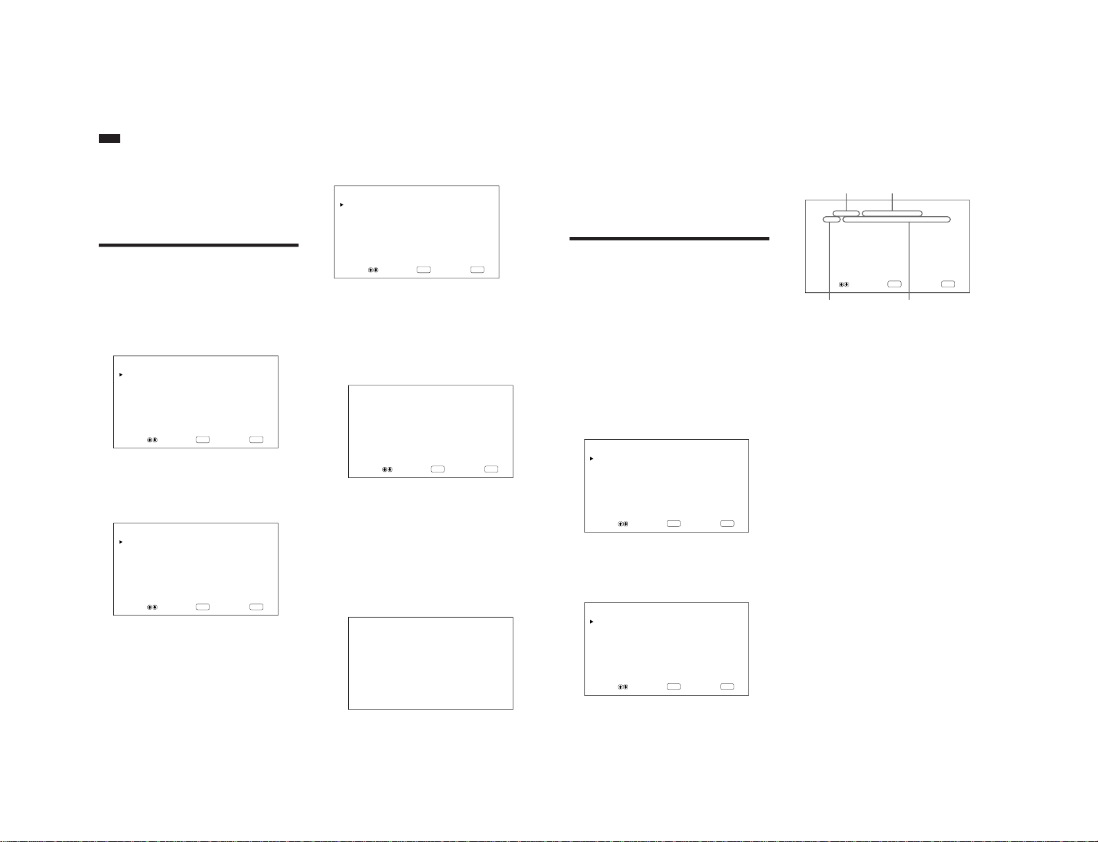
PFM-500A3WE/500A3WG/500A3WU/510A2WE/510A2WG/510A2WU
28
(GB)
Note
If you use the wide zoom mode, it is recommended
that you set the H SIZE, H SHIFT, V SIZE and V
SHIFT to the standard (00) . If you change them too
much, the wide zoom display may be distorted. Before
you use the wide zoom mode, set ZOOM to ×1. If
ZOOM is set to ×2, ×3 or ×4, the wide zoom mode
cannot be used.
Adjusting the Pixels
If there is too much noise on the edges of the
characters or the vertical lines, you can adjust the dot
phase and total number of horizontal pixels.
1
Press MENU.
The main menu appears on the monitor screen.
ENTER
MENU
MA I N MENU
P I C CONT ROL
PIC SIZE
CONF I G
MEMORY
REMOTE
STATUS
SELECT SET END
2
Press M/m to move the cursor (B) to “PIC SIZE”
and press ENT.
The PIC SIZE menu appears on the monitor
screen.
ENTER
MENU
PIC SIZE
HSIZE : 00
HSHIFT : 00
VSIZE : 00
VSHIFT : 00
RESET
ASPECT : 4X3
ZOOM : X1
PIXEL ADJUST
SELECT SET END
3
Press M/m to move the cursor (B) to “PIXEL
ADJUST” and press ENT.
The following menu appears on the monitor
screen.
ENTER
MENU
PIXEL ADJUST
AUTO
DOT PHASE : 50
TOTAL H P IXEL : 80 0
RESET
SELECT SET END
4
You can adjust the dot phase and total number of
horizontal pixels automatically or manually.
Adjusting automatically
(1) Select AUTO with M/m and press ENT.
The following menu appears on the monitor
screen.
ENTER
MENU
PIXEL ADJUST
AUTO : NO
SELECT SET END
(2) Select YES with M/m and press ENT.
The dot phase and total number of horizontal
pixels are adjusted automatically.
Adjusting manually
(1) Select DOT PHASE or TOTAL H PIXEL
with M/m and press ENT.
The following menu appears on the monitor
screen. (The illustration below is for selecting
the DOT PHASE.)
DOT PHASE : 50
Resizing and Positioning the Picture / Adjusting the Pixels
29
(GB)
(2) Adjust the dot phase or total number of
horizontal pixels with M/m and press ENT.
To restore PIXEL ADJUST menu items to their
original settings
In the PIXEL ADJUST menu, press M/m to move the
cursor (B) to “RESET” and press ENT. Then select
YES with M/m and press ENT.
Using the Memory
Function
You can save the current picture setting for each input
signal using the MEMORY function. The saved
settings can be restored whenever necessary. The
items in the PIC CONTROL and PIC SIZE menus can
be memorized. You can save the picture settings of up
to twenty input signals. You can name the settings of
the items (up to 10 characters in length).
Storing the Current Setting
1
Press MENU.
The main menu appears on the monitor screen.
ENTER
MENU
MA I N MENU
P I C CONT ROL
PIC SIZE
CONF I G
MEMORY
REMOTE
STATUS
SELECT SET END
2
Press M/m to move the cursor (B) to “MEMORY”
and press ENT.
The MEMORY menu appears on the monitor
screen.
ENTER
MENU
MEMORY
LOAD
SAVE
SELECT SET END
3
Press M/m to move the cursor (B) to “SAVE” and
press ENT.
The following menu appears on the monitor
screen.
ENTER
MENU
SAVE /No . 01 [··········]
-RGB/
fH
31.5
kHz
/fV59.9
Hz
/POL[N/N]-
SAVE EXECUTE
NAME SE T
SELECT SET END
If there is no data in the selected memory number,
the “– – EMPTY – –” message appears on the
monitor screen in cyan. The signal type and the
color system or horizontal/vertical frequency are
displayed in cyan (showing that the signal type of
the selected memory number is the same as that of
the current setting) or in yellow (showing that the
signal type of the selected memory number is not
the same as that of the current setting).
4
Select a memory number (01 to 20) with M/m and
press ENT.
The cursor (B) appears on the monitor screen.
5
Press M/m to move the cursor (B) to “SAVE
EXECUTE” and press ENT.
The current data is stored under the selected
memory number. The “SAVE COMPLETED”
message appears for about five seconds.
When you name the setting, follow the steps
below.
Signal type
Color system or horizontal/
vertical frequency
Memory number Setting name
Adjusting the Pixels / Using the Memory Function
1-15
Page 24
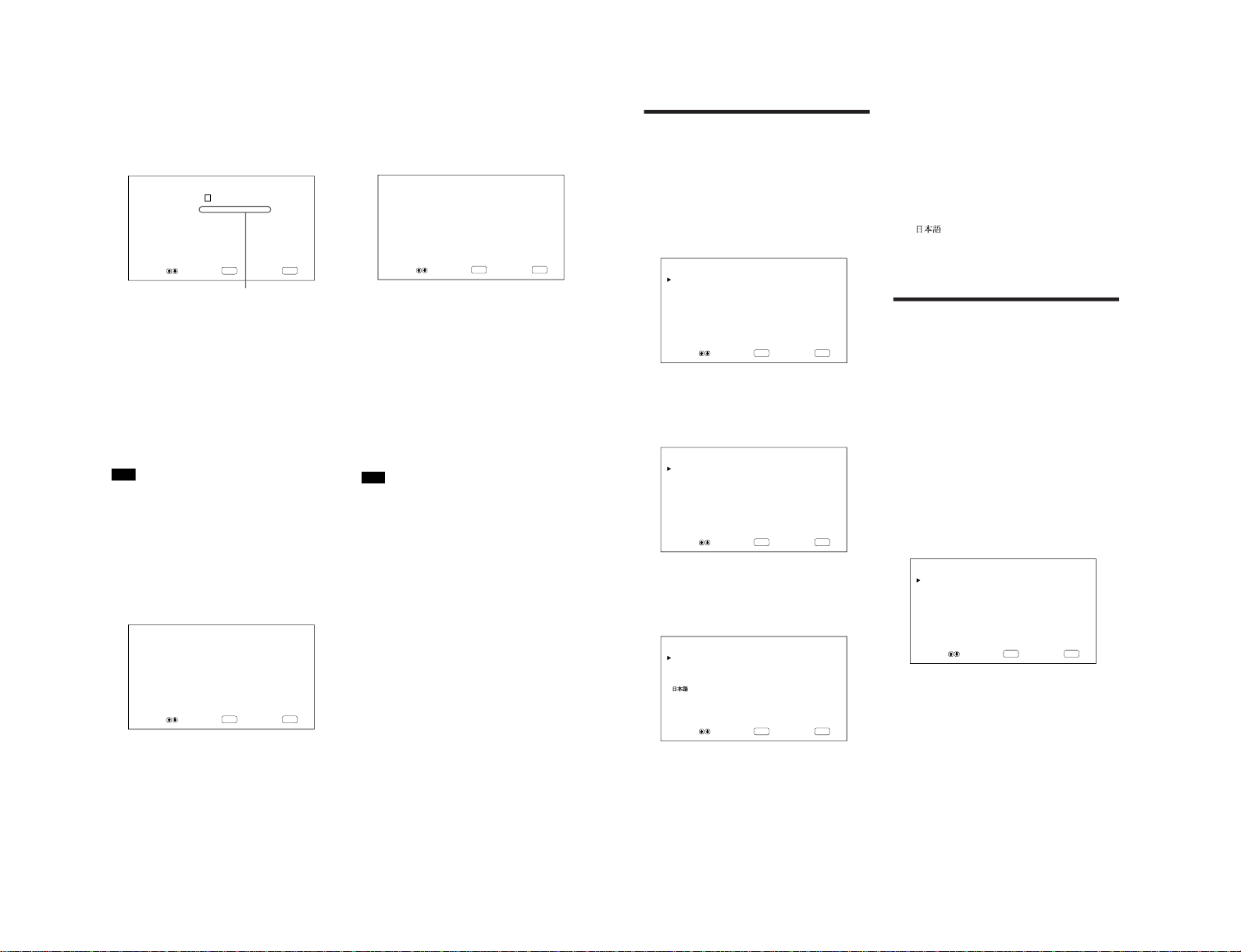
1-16
30
(GB)
6
Press M/m to move the cursor (B) to “NAME
SET” and press ENT.
The following menu appears on the monitor
screen.
ENTER
MENU
SAVE /No . 01 [··········]
NAME SE T : [ ü V v b B ·
fH
fV%.:]
SELECT SET END
7
Select the character to be changed with M/m and
press ENT.
The background of a character in the character list
changes to cyan.
8
Select a character in the character list with M/m
and press ENT.
The selected character is input.
9
Repeat steps 7 and 8 until you finish inputting the
name, then press MENU.
The menu returns to the SAVE menu.
Note
If the storing of the setting fails, the “SAVE ERROR”
message appears on the monitor screen. Try to store
the setting again.
Calling Up a Stored Setting
1
In the MEMORY menu, press M/m to move the
cursor (B) to “LOAD” and press ENT.
The first page of the stored settings appears on the
monitor screen.
ENTER
MENU
LOAD/No.01 [··········]
-RGB/
fH
31.5
kHz
/fV59.9Hz/POL[N/N]CONTRAST : 80
BRI GHTNESS : 00
COLOR TEMP : H I GH
HSIZE : 00
HSHIFT : 00
VSIZE : 00
VSHIFT : 00
ASPECT : 4X3
ZOOM : X1
SELECT VERI FY END
2
Select a memory number (01 to 20) with M/m and
press ENT.
The second page of the stored settings appears on
the monitor screen.
ENTER
MENU
LOAD/No.01 [··········]
-RGB/
fH
31.5
kHz
/fV59.9Hz/POL[N/N]CHROMA : 0 0
PHASE : 00
P ICTURE AGC : ON
SHARPNESS : MI D
H LINEARITY : 00
V LINEARITY : 00
DOT PHASE : 50
TOTAL H P IXEL : 80 0
SELECT SET END
The signal type and the color system or horizontal/
vertical frequency are displayed in cyan (showing
that the signal type of the selected memory
number is the same as that of the current setting
and you can call up the stored setting) or in red
(showing that the signal type of the selected
memory number is not the same as that of the
current setting and you cannot call up the stored
setting).
3
Press ENT.
The “LOAD COMPLETED” message appears for
about five seconds and the picture is adjusted to
the selected setting.
Note
If the loading fails, the “LOAD ERROR” message
appears on the monitor screen. Try to load the setting
again.
Using the Memory Function
Character list
31
(GB)
Selecting the On-screen
Language
You can select the on-screen language from among
English, German, French, Italian, Spanish or
Japanese.
1
Press MENU.
The main menu appears on the monitor screen.
ENTER
MENU
MA I N MENU
P I C CONT ROL
PIC SIZE
CONF I G
MEMORY
REMOTE
STATUS
SELECT SET END
2
Press M/m to move the cursor (B) to “CONFIG”
and press ENT.
The CONFIG menu appears on the monitor
screen.
ENTER
MENU
CONF I G
DI SPLAY : ON
CLOSED CAPT ION: OFF
COLOR SYSTEM : AUTO
SCREEN F I L L : CENTER
POWER CONTROL
SCREEN SAVER
TIME SET
LA NGUAGE
SELECT SET END
3
Press M/m to move the cursor (B) to
“LANGUAGE” and press ENT.
The following menu appears on the monitor
screen.
ENTER
MENU
LA NGUAGE
ENGL I SH
DEUTSCH
FRANÇA IS
ITALIANO
ESPAÑOL
SELECT SET END
4
Press M/m to move the cursor (B) to the desired
language and press ENT.
The on-screen language is switched to the one you
selected.
ENGLISH: English
DEUTSCH: German
FRANÇAIS: French
ITALIANO: Italian
ESPAÑOL: Spanish
: Japanese
5
Press MENU.
The menu returns to the CONFIG menu.
Reducing Afterimage/
Ghosting (Screen Saver
Function)
If a bright image that does not change is displayed on
a screen (e.g., PC) for a long time, an afterimage
(ghosting) may occur. To reduce this afterimage, this
monitor has a screen saver function. The screen saver
function has two screen savers. One screen saver
reverses the image (PIC INVERSION) while the other
automatically changes the display position (PIC
ORBITING).
Reversing the Image
1
Press MENU.
The main menu appears on the monitor screen.
ENTER
MENU
MA I N MENU
P I C CONT ROL
PIC SIZE
CONF I G
MEMORY
REMOTE
STATUS
SELECT SET END
Selecting the On-screen Language / Reducing Afterimage/Ghosting (Screen Saver Function)
PFM-500A3WE/500A3WG/500A3WU/510A2WE/510A2WG/510A2WU
Page 25
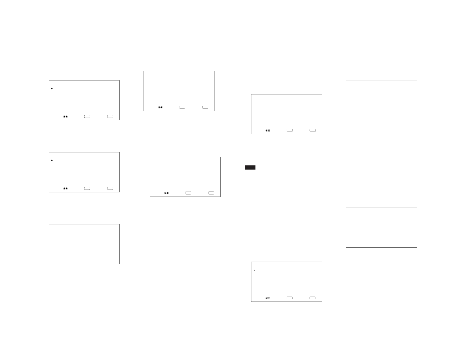
PFM-500A3WE/500A3WG/500A3WU/510A2WE/510A2WG/510A2WU
32
(GB)
2
Press M/m to move the cursor (B) to “CONFIG”
and press ENT.
The CONFIG menu appears on the monitor
screen.
ENTER
MENU
CONF I G
DI SPLAY : ON
CLOSED CAPT ION: OFF
COLOR SYSTEM : AUTO
SCREEN F I L L : CENTER
POWER CONTROL
SCREEN SAVER
TIME SET
LA NGUAGE
SELECT SET END
3
Press M/m to move the cursor (B) to “SCREEN
SAVER” and press ENT.
The following menu appears on the monitor
screen.
ENTER
MENU
SCREEN SAVER
PIC INVERSION : OFF
PIC ORBITING
SELECT SET END
4
Press M/m to move the cursor (B) to “PIC
INVERSION” and press ENT.
The following menu appears on the monitor
screen.
PIC INVERSION : OFF
5
Select the PIC INVERSION mode.
OFF: to set the PIC INVERSION to OFF
ON: to set the PIC INVERSION to ON
AUTO: Carry out the PIC INVERSION process
once a day.
When you select AUTO, the following menu
appears.
ENTER
MENU
PIC INVERSION : AUTO
START T IME : 1 6: 30
END TIME : 16: 45
POWER OFF : NO
SELECT ADJUST END
(1) Press ENT.
The cursor (B) appears on the monitor screen.
(2) Press M/m to move the cursor (B) to “START
TIME” and press ENT.
The following menu appears and the
background of the hour is displayed in cyan.
ENTER
MENU
PIC INVERSION : AUTO
START T IME : 1 6: 30
SELECT SET END
(3) Set the hour when the image is to be reversed
with M/m and press ENT.
The hour is defined and the background of the
minute is displayed in cyan.
(4) Set the minute with M/m and press MENU.
The minute is defined and the menu returns to
the PIC INVERSION menu.
(5) Similarly, set the time when the PIC
INVERSION function is to be cancelled.
The display will be reversed at the START
TIME and will return to the original display at
the END TIME. This cycle is carried out
automatically once a day.
Reducing Afterimage/Ghosting (Screen Saver Function)
33
(GB)
To set the change to the standby mode at the
END TIME
1
After selecting AUTO for PIC INVERSION
mode, select POWER OFF and press ENT.
The following menu appears on the monitor
screen.
ENTER
MENU
PIC INVERSION : AUTO
POWER OFF : NO
SELECT SET END
2
Select YES with M/m and press MENU.
The monitor changes to standby mode at the
designated END TIME.
Notes
•The power off function, power saving function and
on/off timer function in the POWER CONTROL
menu cannot be used simultaneously. When one of
those functions is set to YES, “– – – –” appears next
to the others and their functions are not available.
•If you set START TIME and END TIME to the same
time, the setting of START TIME takes priority over
that of END TIME. The display does not return to
the original display at the END TIME.
Changing the Display Position
Automatically
1
In the SCREEN SAVER menu, press M/m to
move the cursor (B) to “PIC ORBITING” and
press ENT.
The following menu appears on the monitor
screen.
ENTER
MENU
PIC ORBITING
ORB I T I NG : O FF
ORBIT RANGE : 5do t
ORBIT CYCLE : 10sec
SELECT SET END
2
Press M/m to move the cursor (B) to
“ORBITING” and press ENT.
The following menu appears on the monitor
screen.
ORB I T I NG : O FF
3
Select the ORBITING mode with M/m.
OFF: Cancel the PIC ORBITING function.
ON: Set the PIC ORBITING function.
4
Press MENU.
The menu returns to the PIC ORBITING menu.
5
Select ORBIT RANGE (moving distance) or
ORBIT CYCLE (time) with M/m and press ENT.
The following values can be selected:
ORBIT RANGE: 5dot, 10dot, 15dot, 20dot
ORBIT CYCLE: 10sec, 30sec, 1min, 5min
The following menu appears on the monitor
screen. (The illustration below is for selecting
ORBIT RANGE.)
ORBIT RANGE : 5do t
6
Adjust the ORBIT RANGE or ORBIT CYCLE
with M/m and press MENU.
When both PIC INVERSION and PIC
ORBITING are set to ON
If the PIC ORBITING function is actuated while the
picture is reversed, the reversed picture is displayed
changing position.
Reducing Afterimage/Ghosting (Screen Saver Function)
1-17
Page 26
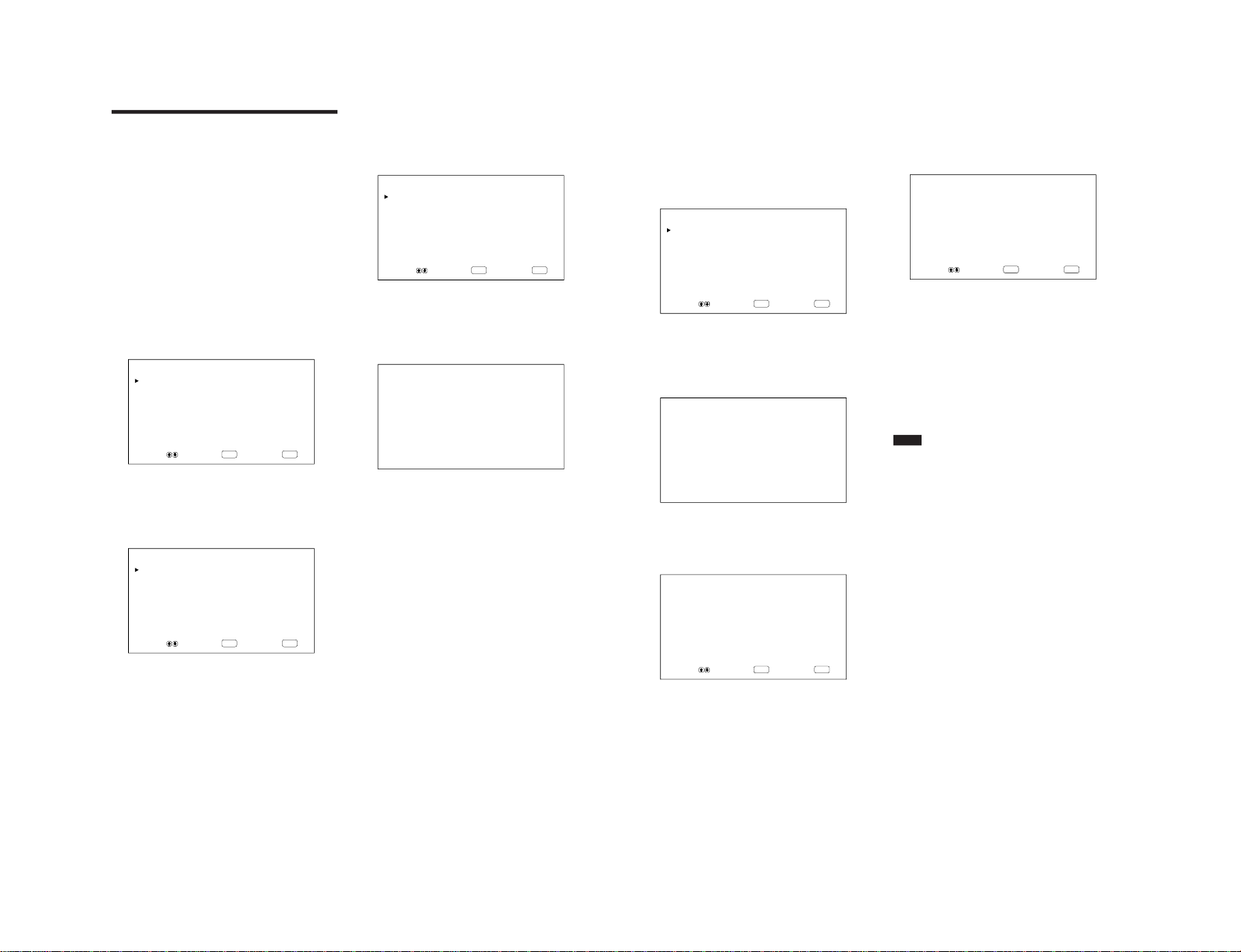
1-18
34
(GB)
Controlling Power On/Off
Automatically (Power
Control Function)
This monitor has two power controlling functions.
You can set it to turn off the power automatically after
a certain period if there is no input signal from the
RGB1 or RGB2 connectors (POWER SAVING
function). You can set the time when the power
automatically turns on/off (ON/OFF TIMER
function).
Power Saving Function
1
Press MENU.
The main menu appears on the monitor screen.
ENTER
MENU
MA I N MENU
P I C CONT ROL
PIC SIZE
CONF I G
MEMORY
REMOTE
STATUS
SELECT SET END
2
Press M/m to move the cursor (B) to “CONFIG”
and press ENT.
The CONFIG menu appears on the monitor
screen.
ENTER
MENU
CONF I G
DI SPLAY : ON
CLOSED CAPT ION: OFF
COLOR SYSTEM : AUTO
SCREEN F I L L : CENTER
POWER CONTROL
SCREEN SAVER
TIME SET
LA NGUAGE
SELECT SET END
Controlling Power On/Off Automatically (Power Control Function)
3
Press M/m to move the cursor (B) to “POWER
CONTROL” and press ENT.
The following menu appears on the monitor
screen.
ENTER
MENU
POWER CONTROL
POWER SAVI NG : OFF
ON / OF F T I ME R : OF F
SELECT SET END
4
Press M/m to move the cursor (B) to “POWER
SAVING” and press ENT.
The following menu appears on the monitor
screen.
POWER SAVI NG : OFF
5
Press M/m to select the length of the time until the
change to power saving mode.
OFF: The power saving function does not work.
5min: Change to the power saving mode after
five minutes if there is no input signal.
10min: Change to the power saving mode after
10 minutes if there is no input signal.
The power indicator flashes when the unit is in the
power saving mode.
To cancel the power saving function
•Input the sync signal again.
•Press the 1 switch on the control panel or the
POWER switch on the Remote Commander.
Signal specification for using the power
saving function
RGB1: When the sync signal is connected to the
HD/COMP IN connector.
RGB2: When the sync signal is connected to the
13th pin of the RGB IN (D-sub 15-pin)
connector.
35
(GB)
On/Off Timer Function
1
In the CONFIG menu, Press M/m to move the
cursor (B) to “POWER CONTROL” and press
ENT.
The following menu appears on the monitor
screen.
ENTER
MENU
POWER CONTROL
POWER SAVI NG : OFF
ON / OF F T I ME R : OF F
SELECT SET END
2
Press M/m to move the cursor (B) to “ON/OFF
TIMER” and press ENT.
The following menu appears on the monitor
screen.
ON / OF F T I ME R : OF F
3
Select ON with M/m and press ENT.
The following menu appears on the monitor
screen.
ENTER
MENU
ON / OF F T I ME R : ON
ON T I ME : 1 6 : 3 0
OFF T IME : 17 :20
SELECT ADJUST END
4
Press ENT.
The cursor (B) appears on the monitor screen.
Controlling Power On/Off Automatically (Power Control Function)
5
Press M/m to move the cursor (B) to “ON TIME”
and press ENT.
The following menu appears and the background
of the hour is displayed in cyan.
ENTER
MENU
ON / OF F T I ME R : ON
ON T I ME : 1 6 : 3 0
SELECT SET END
6
Set the hour with M/m and press ENT.
The hour is defined and the background of the
minute is displayed in cyan.
7
Set the minute with M/m and press MENU.
The minute is defined and the menu returns to the
ON/OFF TIMER menu.
8
Similarly, set the OFF TIME.
Notes
•The power saving function does not work when the
signal is input from the LINE connectors.
•If the sync signal is not connected to the HD/COMP
IN connector, the monitor does not turn on even if
the sync signal is input. Be sure to set POWER
SAVING to OFF when only the RGB signal is
connected.
•If the sync signal is not connected to the 13th pin of
the RGB IN (D-sub 15-pin) connector, the monitor
does not turn on even if the sync signal is input. Be
sure to set POWER SAVING to OFF when only the
RGB signal is connected.
•The power saving function, on/off timer function and
power off function in the PIC INVERSION mode
cannot be used simultaneously. When one of those
functions is set to ON, “– – – –” appears next to the
others and their functions are not available.
•If you set ON TIME and OFF TIME to the same
time, the setting of ON TIME takes priority over that
of OFF TIME. The monitor does not turn off at the
OFF TIME.
PFM-500A3WE/500A3WG/500A3WU/510A2WE/510A2WG/510A2WU
Page 27
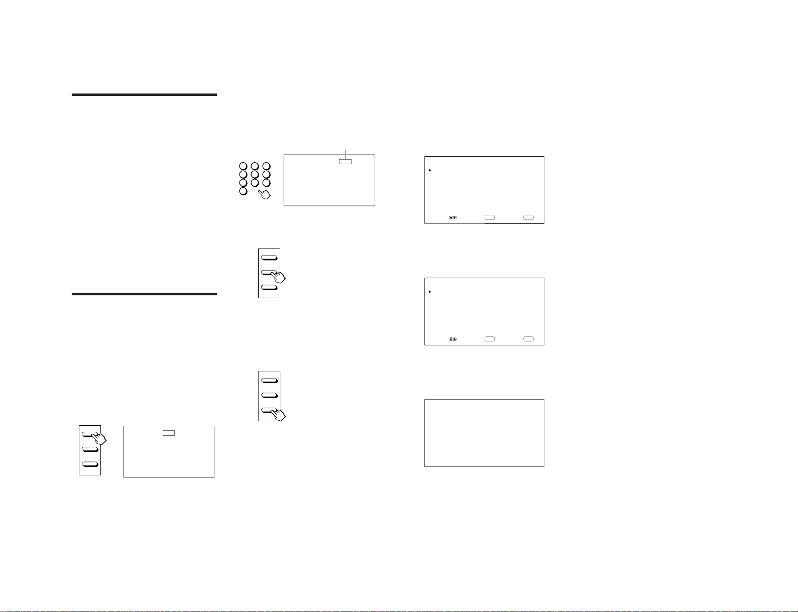
PFM-500A3WE/500A3WG/500A3WU/510A2WE/510A2WG/510A2WU
36
(GB)
Self-diagnosis Function
The unit has a self-diagnosis function.
This function displays the monitor’s condition with
the 1 indicator flashing and numbers on the
SERVICE CODE indicator on the left connector
panel. The numbers inform you of the monitor’s
current condition.
When the unit is working properly, only the dot at the
lower-right position on the SERVICE CODE indicator
flashes.
If the 1 indicator flashes, check the number and
contact your authorized Sony dealer.
1
Check the two-digit number on the SERVICE
CODE indicator.
The indicator shows one number, or multiple
numbers alternately in one second intervals.
2
Unplug the unit.
Inform your authorized Sony dealer of the
number.
Operating a Specific Monitor
With the Remote Commander
Using the supplied Remote Commander, you can
operate a specific monitor without affecting other
monitors that are installed at the same time.
1
Press ID MODE ON on the Remote Commander.
Monitor index numbers appear in white characters
on all the monitors. (Every monitor is allocated an
individual preset index number from 1 to 255.)
See “To change the index number” in the left-hand
column on the next page to change the index number.
ON
ID MODE
SET
OFF
INDEX No. 117 . ..
Self-diagnosis Function / Operating a Specific Monitor With the Remote Commander
2
Input the index number of the monitor you want to
operate using the 0 – 9 buttons on the Remote
Commander.
The input number appears right next to the index
number of each monitor.
2
5
8
3
6
9
1
4
7
10/0
INDEX No. 117 117
3
Press ID MODE SET.
The character on the selected monitor changes to
cyan while others change to red.
ON
ID MODE
SET
OFF
You can operate only the monitor specified. (All
operations are available in ID mode except
POWER ON/OFF.)
4
After the necessary adjustment, press ID MODE
OFF.
The monitor returns to the normal mode.
ON
ID MODE
SET
OFF
Input number
Index number
37
(GB)
To change the index number
You can change the index number if necessary.
When you change the number, use the buttons on the
monitor.
1
Press MENU.
The main menu appears on the monitor screen.
ENTER
MENU
MA I N MENU
P I C CONT ROL
PIC SIZE
CONF I G
MEMORY
REMOTE
STATUS
SELECT SET END
2
Press M/m to move the cursor (B) to “REMOTE”
and press ENT.
The REMOTE menu appears on the monitor
screen.
ENTER
MENU
REMOTE
INDEX No. : 001
REMOTE MODE : TV
REMOTE ONLY : OFF
SELECT SET END
3
Press M/m to move the cursor (B) to “INDEX
No.” and press ENT.
The following menu appears on the monitor
screen.
INDEX No. : 001
4
Select the index number with M/m and press ENT.
The menu returns to the REMOTE menu.
Operating a Specific Monitor With the Remote Commander
1-19
Page 28
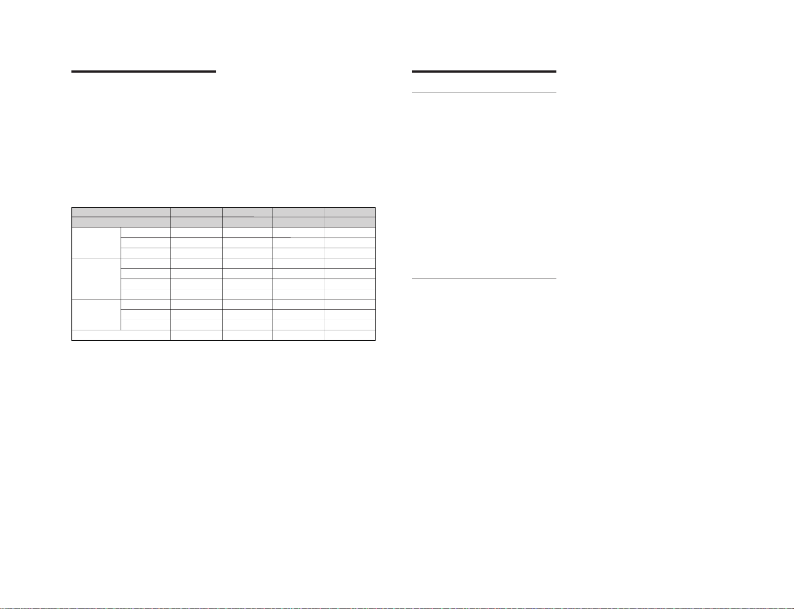
1-20
38
(GB)
Remote Commander model RM-854 RM-1271 RM-PJ1292 RM-PJ1000
REMOTE MODE setting TV PJ PJ PJ
Input selection RGB1 RGB A A A
RGB2 — B B B
LINE LINE1 VIDEO VIDEO VIDEO
Menu operation MENU MENU PAGE or < PAGE or < MENU or <
ENTER ENTER ,,ENTER or ,
++MMM
––mmm
Picture adjustment Contrast CONTRAST+/– CONTR+/– CONTR+/– CONTR+/–
Chroma CHROMA+/– COLOR+/– COLOR+/– COLOR+/–
Phase PHASE+/– HUE+/– HUE+/– HUE+/–
On-screen information DISPLAY — STATUS ON STATUS ON
Using Other Remote Commander Models
Using Other Remote
Commander Models
The following operations can be carried out.
•Power on/off
•Input selection
•Menu operations
•Picture adjustments: contrast, phase and chroma
•On-screen display on/off
The operations available and the buttons to be used
for each operation are limited depending on each
Remote Commander. See the table below.
39
(GB)
Specifications
Video processing
Preset signal Input: formats (See page
22 (GB).)
Sampling rate 13.5 to 140 MHz
Panel system AC-type Plasma Display Panel
Display resolution 510A2W: 1 024 dots × 1 024 lines
500A3W: 852 dots × 480 lines
Pixel pitch 510A2W:
0.90 (horizontal) × 0.51
(vertical) mm
(1⁄16 × 1⁄32 inches)
500A3W:
1.08 (horizontal) × 1.08
(vertical) mm
(1⁄16 × 1⁄
16
inches)
Picture size 510A2W:
921 (horizontal) × 522
(vertical) mm
(36 3⁄8 × 20
5
⁄
8
inches)
500A3W:
920 (horizontal) × 518
(vertical) mm
(36
1
⁄4 × 20 1⁄
2
inches)
Panel size 510A2W: 42-inch (diagonal 1 058
mm)
500A3W: 42-inch (diagonal 1 056
mm)
Inputs and Outputs
RGB1
R (R-Y)/ G (Y)/B (B-Y) IN
BNC-type (×3)
0.714 Vp-p/non-composite 75-ohm
(automatic termination)
1 Vp-p/composite 75-ohm
(automatic termination)
SYNC IN (HD/COMP, VD)
BNC-type (×2)
H (or composite) SYNC, V SYNC,
1 to 5 Vp-p high impedance
AUDIO IN (L, R) Phono jack (×2)
500 mVrms, high impedance
R (R-Y)/ G (Y)/B (B-Y) OUT
BNC-type (×3) Loop-through
SYNC OUT (HD/COMP, VD)
BNC-type (×2) Loop-through
H (or composite) SYNC,
V SYNC
AUDIO OUT (L, R)
Phono jack (×2) Loop-through
RGB2
RGB IN D-sub 15-pin (See “Pin
assignment” on page 40 (GB).)
AUDIO IN (L, R) Phono jack (×2)
500 mVrms, high impedance
LINE (NTSC, PAL, SECAM, NTSC4.43, PAL60)
VIDEO IN BNC-type (×1)
Composite video, 1 Vp-p ±2 dB
sync negative, 75-ohm
(automatic termination)
Y/C IN Mini DIN 4-pin type (×1)
Y (luminance): 1 Vp-p ±2 dB sync
negative, 75-ohm (automatic
termination)
C (chrominance): Burst
0.286 Vp-p ±2 dB (NTSC),
75-ohm (automatic termination)
Burst 0.3 Vp-p ±2 dB (PAL),
75-ohm (automatic termination)
AUDIO IN (L, R) Phono jack (×2)
500 mVrms, high impedance
VIDEO OUT BNC-type (×1) Loop-through
Y/C OUT Mini DIN 4-pin type (×1) Loop-
through
AUDIO OUT (L, R)
Phono jack (×2) Loop-through
MONITOR OUT AUDIO (L, R)
Phono jack (×2)
Maximum 500 mVrms (Variable
output), high impedance
CONTROL S (IN, OUT)
Mini jack (stereo) (×2)
5 Vp-p
REMOTE (RS-232C)
Mini DIN 8-pin type (×1)
SPEAKERS 6 to 16 ohms, 7 W + 7 W (when
the impedance is 8 ohms)
Specifications
PFM-500A3WE/500A3WG/500A3WU/510A2WE/510A2WG/510A2WU
Page 29
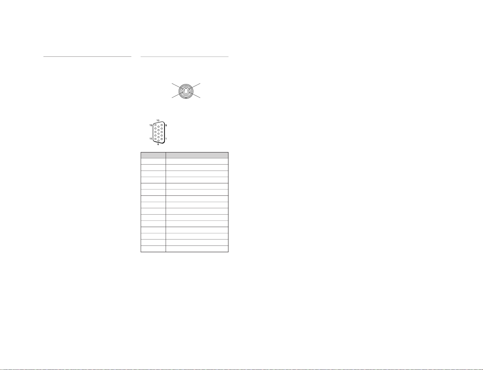
PFM-500A3WE/500A3WG/500A3WU/510A2WE/510A2WG/510A2WU
40
(GB)
Pin No. Signal
1 Red video or R-Y
2 Green video or Y
3 Blue video or B-Y
4 Ground
5 Ground
6 Red ground
7 Green ground
8 Blue ground
9 Not used
10 Ground
11 Ground
12 SDA
13 H sync or composite sync
14 V sync
15 SCL
Chrominance
GND
GND
General
Power requirements
510A2W: 100 to 120 V AC,
50/60 Hz, 4.7 A/410 W
220 to 240 V AC, 50/60 Hz,
2.2 A/400 W
500A3W: 100 to 120 V AC,
50/60 Hz, 3.9 A/380 W
220 to 240 V AC, 50/60 Hz,
2.0 A/360 W
Operating conditions
Temperature: 0 °C to 35 °C
(32 °F to 95 °F)
Humidity: 20% to 90%
(no condensation)
Atmospheric pressure: 700 to
1 060 hPa
Storing/transporting conditions
Temperature: –10 °C to +40 °C
(14 °F to 104 °F)
Humidity: 20% to 90%
(no condensation)
Atmospheric pressure: 700 to
1 060 hPa
Dimensions 1 036 × 636 × 152 mm
(40 7⁄8 × 25
1
⁄8 × 6 inches) (w/h/d)
Mass 45 kg (99 lb 3 oz)
Supplied accessories
AC power cord (1)
AC plug holder (1)
Remote Commander RM-921 (1)
Size AA (R6) batteries (2)
Ferrite core (2)
Foot support bracket (2)
Screws for foot support bracket (6)
Monitor stabilizer (2)
Operating instructions (1)
Design and specifications are subject to change
without notice.
Pin assignment
Y/C jack (Mini DIN 4-pin)
RGB IN connector (D-sub 15-pin)
Specifications
Luminance
1-21
Page 30
1-22
3-864-657-03(1)
Operating Instructions
MB-514
Mounting Bracket
© 1998 by Sony Corporation
Printed in Japan
1-2. MB-514 Operating Instructions
PFM-500A3WE/500A3WG/500A3WU/510A2WE/510A2WG/510A2WU
This section is reprinted
from operation manual.
Page 31
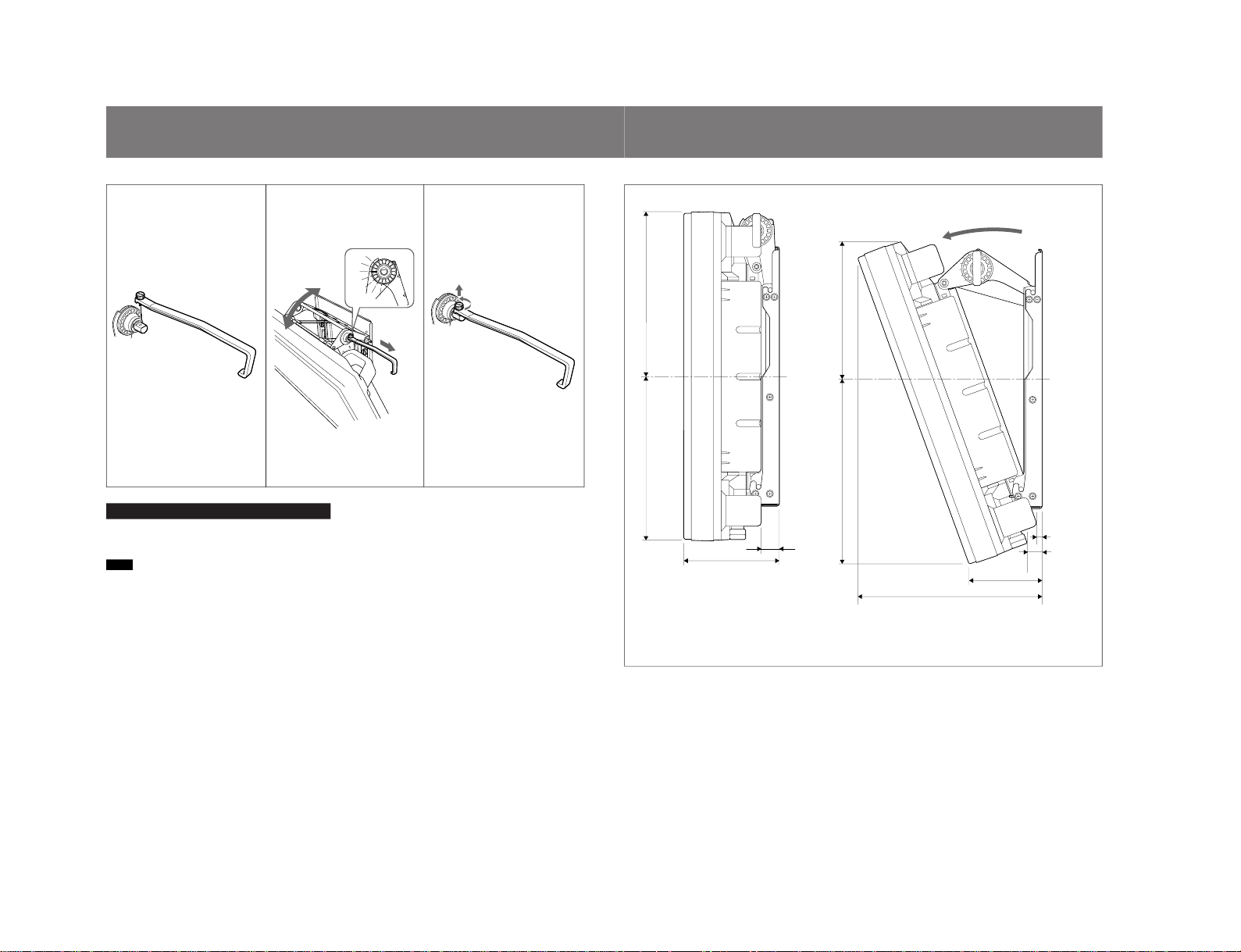
PFM-500A3WE/500A3WG/500A3WU/510A2WE/510A2WG/510A2WU
Changing the Angle of the Monitor
123
English
You can change the angle of the monitor panel by adjusting
the angle of the mounting bracket.
Note
If you have any questions about installing the mounting
bracket, contact your authorized Sony dealer.
1
Attach the handle on the mounting bracket with the
supplied screw (provided with the handle).
2
Adjust the monitor panel angle.
You can change the angle from 0° to 20° (7 levels).
(Approx. 0°, 4°, 8°, 12°, 15°, 18° and 20°)
(1) Pull the handle down to unsnap the lock.
(2) Push the panel to the desired angle.
(3) Let go of the handle and adjust the panel angle so
it can be locked.
See the angle marks.
3
Remove the handle.
Store the handle with the Operating Instructions.
(1)
(2)
(3)
0
4
8
12
15
20
18
Dimensions of the assembled bracket
Design and specifications are subject to change
without notice.
Side view
Units : mm (inches)
317.5 (12
1
/
2
)
35 (1 3/8)
317.5 (12
1
/
2
)
186.6 (7
11
/32)
263 (10
11
/
32
)361 (14
7
/
32
)
360 (14 3/16)
141 (5
9
/16)
10 (
13
/32)
29(1
5
/32)
20° (max.)
1-23
Page 32
1-24
3-864-658-04(1)
Installation Manual for Dealers
1998 by Sony Corporation
MB-514
Mounting Bracket
1-3. MB-514 Installation Manual for Dealers
PFM-500A3WE/500A3WG/500A3WU/510A2WE/510A2WG/510A2WU
This section is reprinted
from installation manual.
Page 33
PFM-500A3WE/500A3WG/500A3WU/510A2WE/510A2WG/510A2WU
2
WARNING
Install the monitor on a wall that can hold a weight of at least 400kg (881lb14 oz). Reinforce the wall, if needed.
3
Table of contents
English
Overview
..................................................................................
5
Parts List
..................................................................................
5
Installation
................................................................................
6
Specifications
........................................................................
12
1-25
Page 34
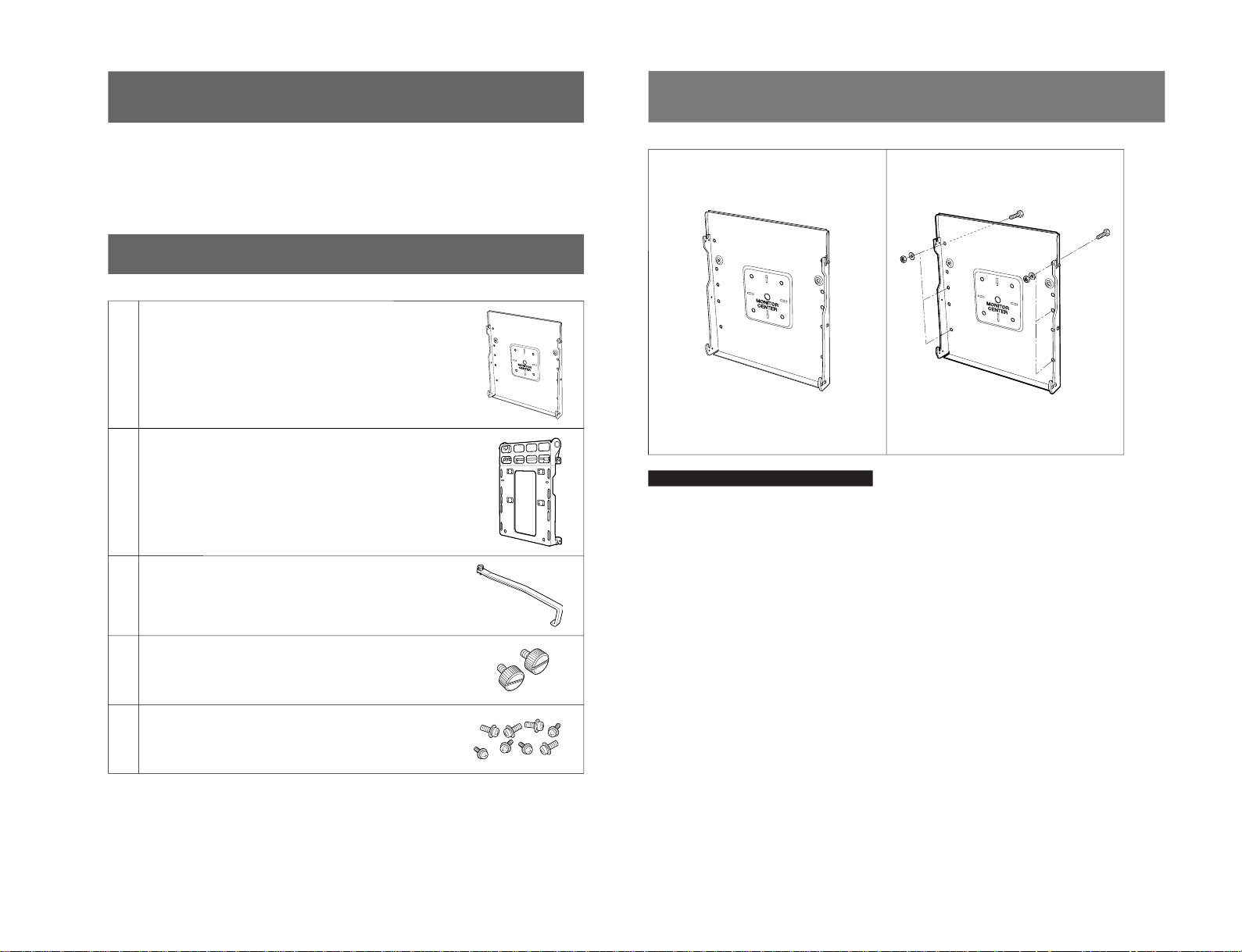
1-26
5
Parts List
Mounting bracket (1)
Wall bracket (1)
Handle (1)
Knob (2)
Screw M5 (8)
(a)
(b)
(c)
(d)
(e)
Overview
The mounting bracket MB-514 is designed to install the Sony flat panel monitor
on a wall.
6
Installation
2
English
1
Decide where on the wall you want to install the
wall bracket (a).
The center hole of the wall bracket will be matched
the center of the monitor panel.
2
Install the wall bracket (a) on the wall.
Use six M8 bolts or concrete anchors, six nuts and
six washers (not supplied).
1
(a)
(a)
PFM-500A3WE/500A3WG/500A3WU/510A2WE/510A2WG/510A2WU
Page 35
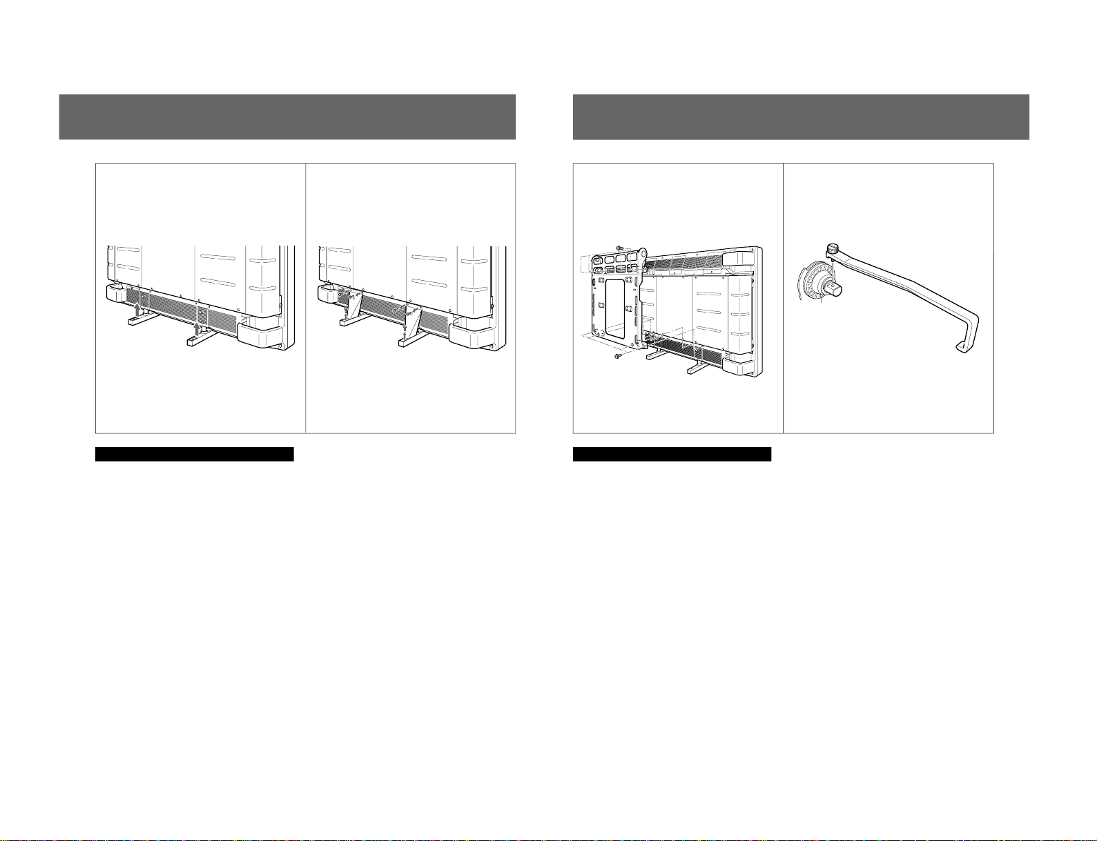
PFM-500A3WE/500A3WG/500A3WU/510A2WE/510A2WG/510A2WU
7
4
3
English
3 Pull down the retractable feet and stand the monitor
up.
For details on using the retractable feet, see the
Operating Instructions for the Sony flat panel
monitor .
If the retractable feet and the foot support brackets
are already installed on the monitor, go to Step 4.
Otherwise, go to Step 5.
4 Remove the foot support brackets from the
retractable feet.
For details on removing the foot support brackets,
see the Operating Instructions for the Sony flat panel
monitor.
8
Installation
English
5 Install the mounting bracket (b) on the flat monitor.
Match the mounting bracket screw holes to the
monitor screw holes, then insert and tighten eight
M5 screws (e) to lock the bracket onto the monitor.
6 Attach the handle (c) on the mounting bracket (b)
with the supplied screw (provided with the handle).
5
6
(b)
(e)
(c)
(b)
1-27
Page 36
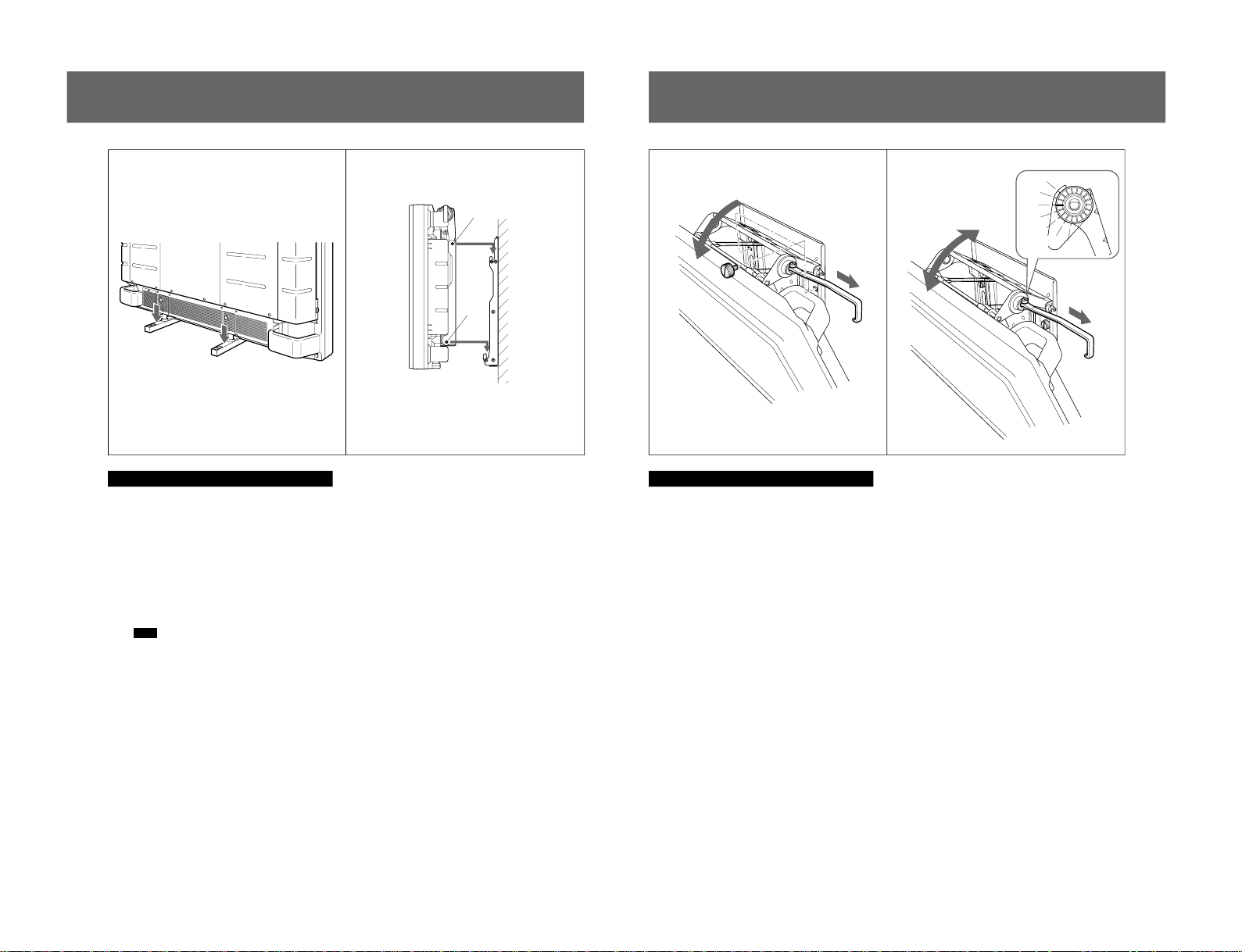
1-28
9
English
7
Store the retractable feet.
For details on using the retractable feet, see the
Operating Instructions for the Sony flat panel
monitor.
8
Install the flat monitor with the mounting bracket (b)
on the wall bracket (a).
Hook two mounting bracket shafts A, B on the
wall bracket grooves.
Note
Make sure that the shafts hook properly into the
grooves.
78
(b)
(a)
A
B
10
Installation
English
9
Lock the mounting bracket shafts (hooked in Step
8) by turning two knobs (d) so that the shafts do
not move vertically.
Pull the handle (c) out (installed in Step 6) and
unsnap the lock. Pull down the monitor panel so
the mounting bracket angle is fully extended. Turn
two knobs (d) and lock the monitor panel.
10
Adjust the monitor panel angle.
You can change the angle from 0° to 20° (7
levels). (Approx. 0°, 4°, 8°, 12°, 15°, 18° and 20°)
(1) Pull the handle (c) down to unsnap the lock.
(2) Push the panel to the desired angle.
(3) Let go of the handle and adjust the panel angle
so it can be locked.
See the angle marks.
9!º
(c)
(d)
(1)
(2)
(c)
(1)
(2)
(3)
0
4
8
12
15
20
18
PFM-500A3WE/500A3WG/500A3WU/510A2WE/510A2WG/510A2WU
Page 37
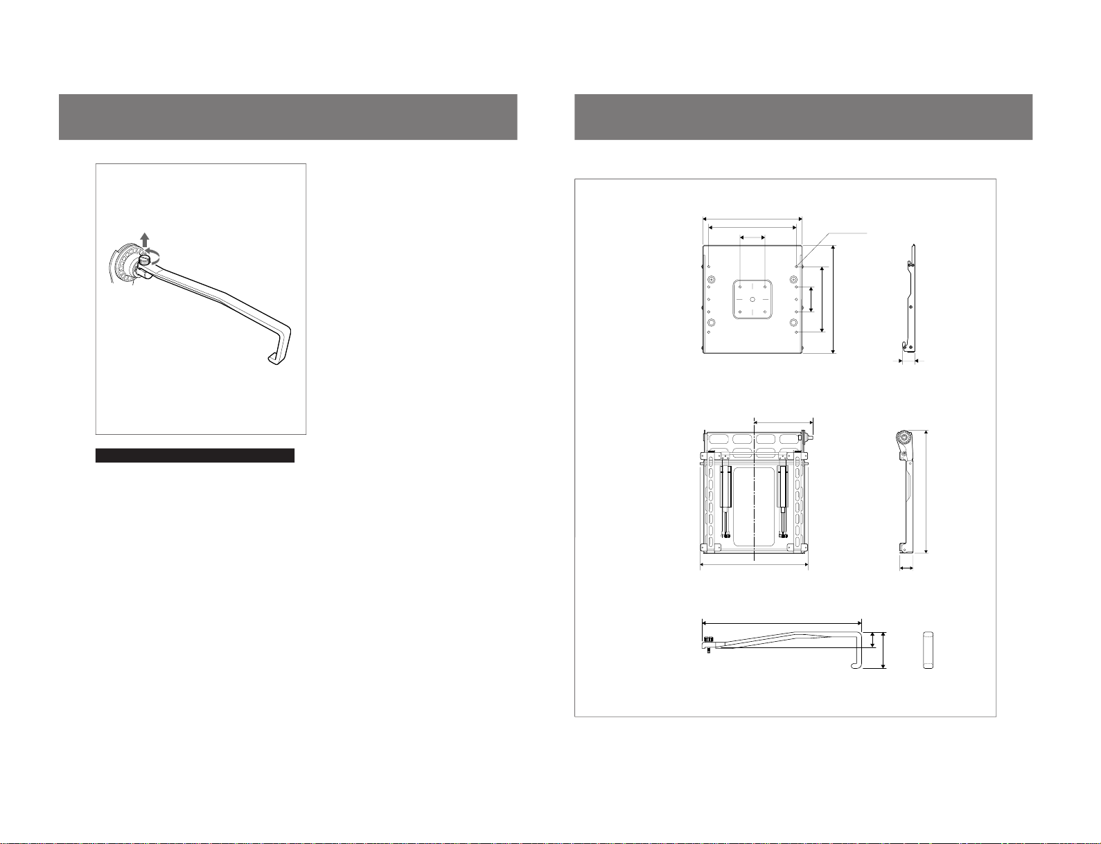
PFM-500A3WE/500A3WG/500A3WU/510A2WE/510A2WG/510A2WU
11
!¡
English
11
Loosen the screw and remove the handle.
Store the handle with the Operating Instructions.
(c)
12
MONITOR
CENTER
Dimensions
Handle
Wall bracket
Specifications
Mounting bracket
(a)
(c)
Units : mm (inches)
(b)
Mass Approx. 5.2kg (11lb7oz)
Mass Approx. 5.8kg (12lb13oz)
Mass Approx. 130g (60oz)
278.3 (10
31
/32)
28 (1
3
/
32
)
65 (2
9
/16)
470 (18
1
/2)
255.4 (10
1
/16)
535 (21
1
/16)
56.5 (2
7
/32)
455 (18 15/16)
406.4 (16)
114.3 (4
1
/2)
114.3 (4
1
/
2
)
304.8 (12)
500 (19
11
/
16
)
57 (2
1
/4)
φ
9.5 (3/8)
1-29
Page 38
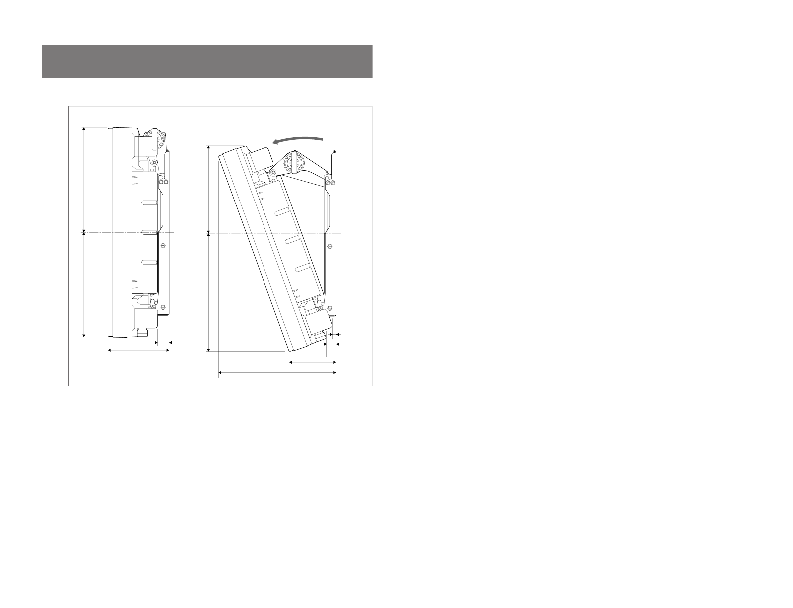
1-30
13
Dimensions of the assembled bracket
Design and specifications are subject to change
without notice.
Side view
Units : mm (inches)
317.5 (12
1
/
2
)
35 (1 3/8)
317.5 (12
1
/
2
)
186.6 (7
11
/32)
263 (10
11
/
32
)361 (14
7
/
32
)
360 (14 3/16)
141 (5
9
/16)
10 (
13
/32)
29 (1
5
/32)
20° (max.)
PFM-500A3WE/500A3WG/500A3WU/510A2WE/510A2WG/510A2WU
Page 39
PFM-500A3WE/500A3WG/500A3WU/510A2WE/510A2WG/510A2WU
4-074-891-01(1)
Input Adaptor
Operating Instructions
BKM-500
Sony Corporation © 1999
Printed in Japan
English
WARNING
Owner’s Record
The model and serial numbers are located on the rear.
Record the model and serial numbers in the spaces
provided below. Refer to these numbers whenever you call
upon your Sony dealer regarding this product.
Model No. BKM-500 Serial No.
To prevent fire or shock hazard, do not
expose the unit to rain or moisture.
Do not open the cabinet.
Refer servicing to qualified personnel
only.
For installation, consult your nearest Sony dealer.
For the customers in the U.S.A
This equipment has been tested and found to comply with
the limits for a Class A digital device, pursuant to Part 15 of
the FCC Rules. These limits are designed to provide
reasonable protection against harmful interference when
the equipment is operated in a commercial environment.
This equipment generates, uses, and can radiate radio
frequency energy and, if not installed and used in
accordance with the instruction manual, may cause harmful
interference to radio communications. Operation of this
equipment in a residential area is likely to cause harmful
interference in which case the user will be required to
correct the interference at his own expense.
You are cautioned that any changes or modifications not
expressly approved in this manual could void your authority
to operate this equipment.
For the customers in Europe
WARNING
This is a Class A product. In a domestic environment this
product may cause radio interference in which case the
user may be required to take adequate measures.
1-4. BKM-500 Operating Instructions
1-31
This section is reprinted
from operation manual.
Page 40

1-32
English
For BKM-500 Users
This Input Adaptor is for the PFM-500A/510A Series
Sony Flat Panel Monitors. You can use the adaptor
after installing it on the monitor.
For details on how to operate the Input Adaptor, refer
to the Operating Instructions for the monitor.
For details on installation, contact your authorized Sony
dealer.
PFM-500A3WE/500A3WG/500A3WU/510A2WE/510A2WG/510A2WU
Page 41
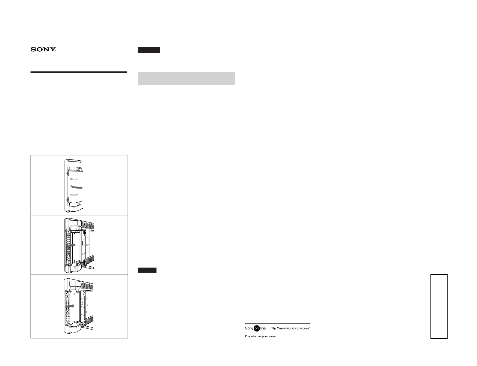
PFM-500A3WE/500A3WG/500A3WU/510A2WE/510A2WG/510A2WU
4-074-892-01 (1)
Input Adaptor
BKM-500
Sony Corporation ©1999 Printed in Japan
A
2
Right side of the
monitor
B
Installation Manual for
Dealers
1
1
3
3
C
2
1
1
English
Follow the steps below to install the Input Adaptor to the
PFM-500A/510A series Flat Panel Monitors.
Installing the Input Adaptor (Figures
A, B
and C)
Before installation
•Before installation, make sure that the power to all the
equipment is off. To turn the monitor completely off, press
the 1 switch so that the monitor changes to standby mode,
then disconnect the power cable from the wall outlet.
•If the monitor has been installed on a wall, remove it from
the wall.
•If you are using the SS-X500A Speaker System, remove
the right speaker.
•Install the Input Adaptor to the monitor on a stable, flat and
horizontal surface. Lock the monitor by using the
retractable feet.
1
On the right side of the monitor, locate the screws that
lock the panel cover on the monitor. Loosen the screws
by turning them counterclockwise and open the cover.
A
If another connector panel has been installed on the
monitor, remove the connector panel as follows:
1 Loosen the two screws that are at the top and bottom
of the right connector panel.
You can now remove the connector panel. B
2 Slowly pull out the connector panel from the
monitor. B
2
First make sure that the direction (top/bottom) of the
Input Adaptor, then correct and insert it into the monitor.
Make sure that the two connectors inside the monitor are
connected firmly. C
3
Tighten the top and the bottom screws. C
4
Connect the required cables. Close the panel cover
(opened in Step 1) and lock it with the cover screws.
Caution
Do not touch the connectors in the monitor. Doing so may
be result in injury to yourself or damage to the connectors.
1-5. BKM-500 Installation Manual for Dealers
This section is reprinted
from installation manual.
1-33
Page 42

Page 43
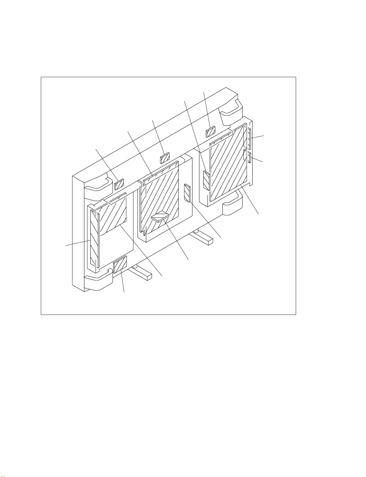
2-1. Circuit Boards Location
B
S1
Section 2
Service Informations
S1
G2
S1
UA
AF
UJ
Switching regulator
(APS-132 M/136 M)
G1
B1
H1
H6
PFM-500A3WE/500A3WG/500A3WU/510A2WE/510A2WG/510A2WU
2-1
Page 44
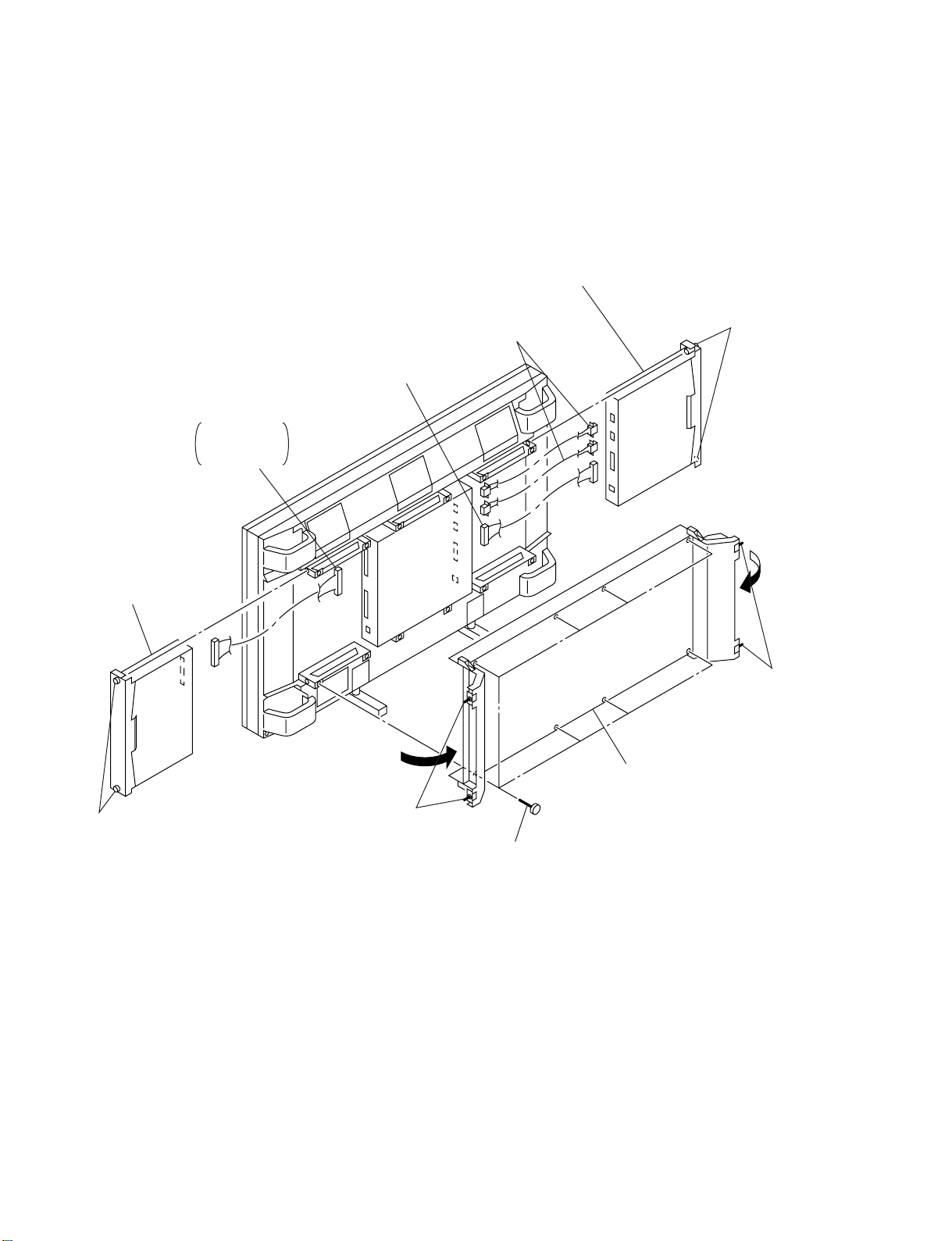
2-2. Disassembly
2-2-1. I/O Block Assy and Power Block Assy Removal and Extension Cable
Connection
8 Power block assy
Note) When removing the switching regulator
from the main unit, start performing more than
30 seconds after the main power is turned off.
6 I/O block assy
Extension cable : 64 pin
A-1501-146-A
or
A-1501-147-A
Extension cable : 8 pin
(1-900-239-54)
Extension cable : 40 pin
(1-900-239-53)
7 Loosen the two screws.
2 Loosen the
two screws.
5 Loosen the two screws.
2-2
4 Rear cover
1 Loosen the two screws.
3 Eight screws
(+PSW4 x 10)
PFM-500A3WE/500A3WG/500A3WU/510A2WE/510A2WG/510A2WU
Page 45
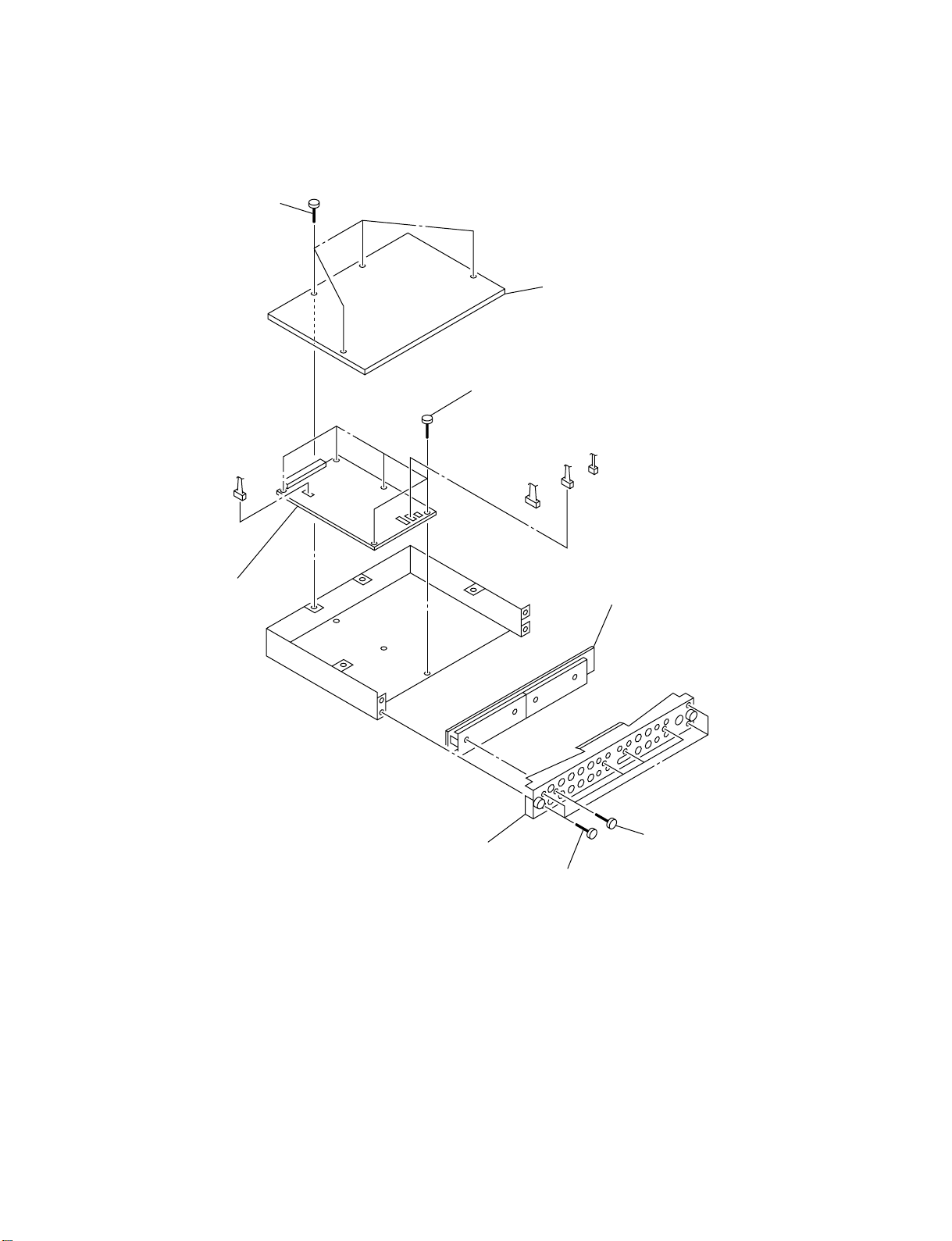
2-2-2. H1 and UJ Boards Removal
1 Four screws
(+PSW3 x 10)
CN105
2 I/O unit cover
3 Five screws
(+PSW3 x 10)
CN102
CN101
CN103
4 H1 board
6 I/O unit panel
8 UJ board
7 Four screws
(+PSW3 x 10)
5 Four screws
(+PSW3 x 10)
PFM-500A3WE/500A3WG/500A3WU/510A2WE/510A2WG/510A2WU
2-3
Page 46
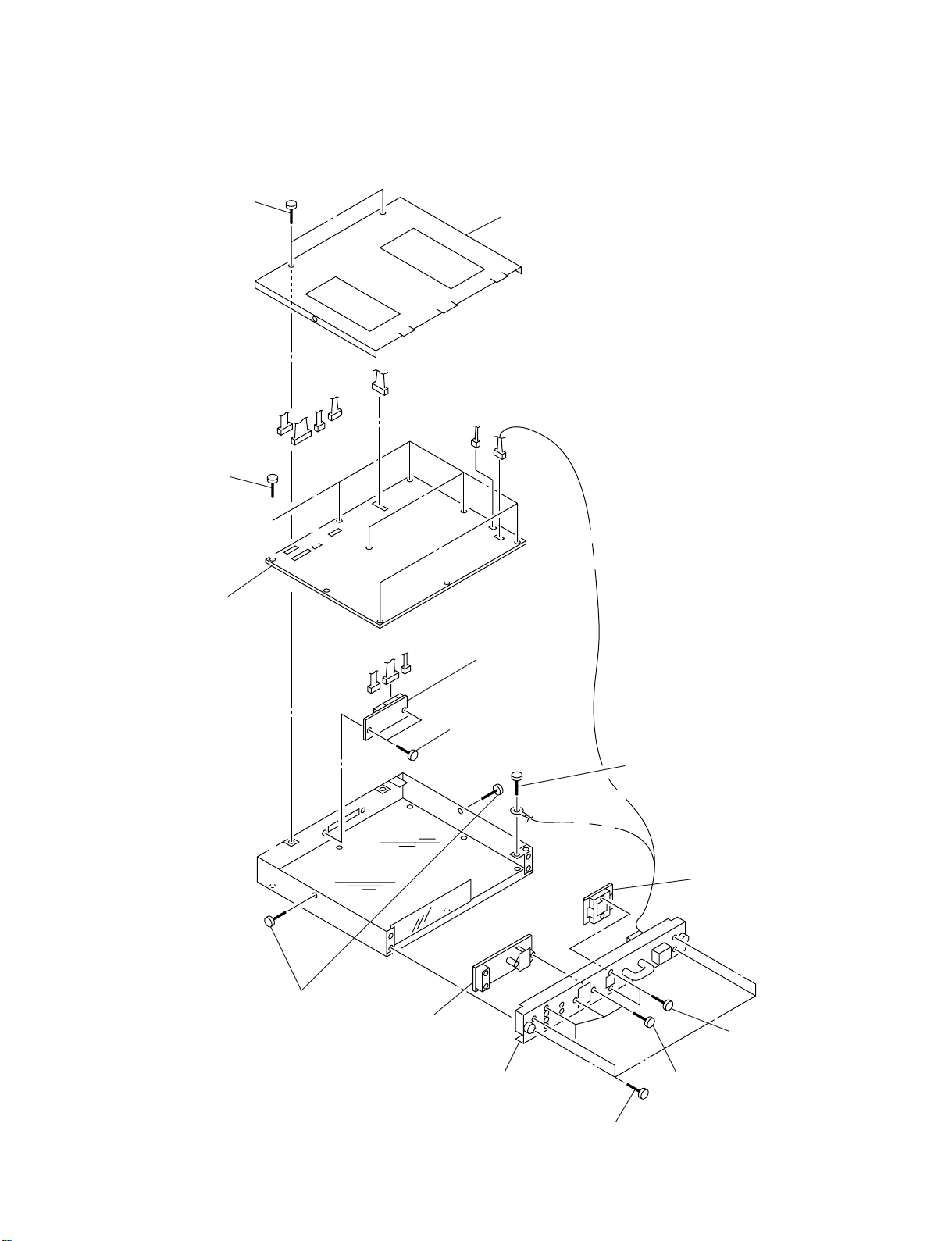
2-2-3. AF, G2, UA Boards and Switching Regulator (APS-132 M/136 M Board)
Removal
2 Two screws
(+PSW3 x 10)
3 Power unit cover
4 Eight screws
(+P4 x 8)
5 Switching regulator
(APS-132 M/136 M board)
CN7
CN8
CN4
CN6
CN4003
CN4008
CN5
CN4005
CN1
CN2
7 G2 board
6 Two screws
(+PSW3 x 10)
8 Screw
(+P4 x 8)
2-4
1 Two screws
(+K3 x 10)
!= UA board
0 Power unit panel
!] AF board
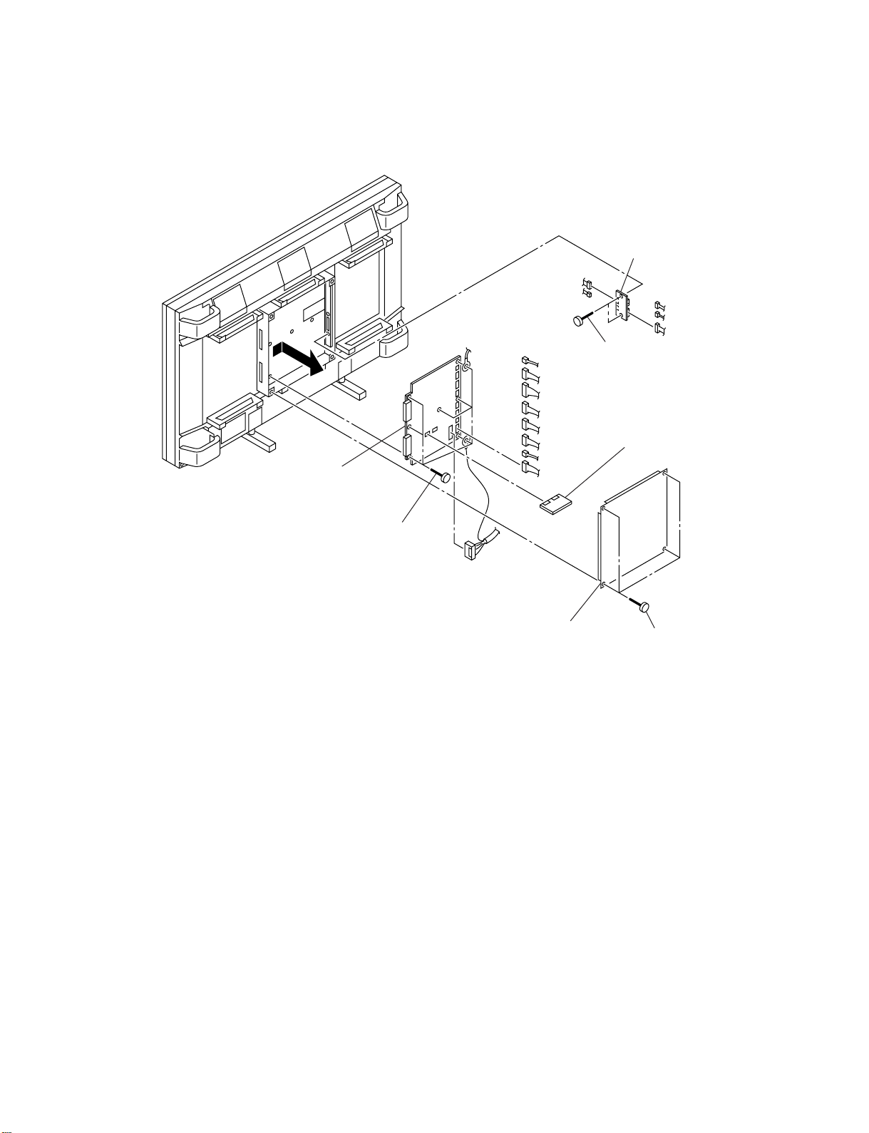
2-2-4. B and G1 Boards Removal
* Remove the Rear cover, I/O block assy and Power block assy. (Refer to 2-2-1.)
4 B board
3 Seven screws
(+PSW3 x 10)
CN3
CN5001
CN5002
CN13
CN14
CN12
CN10
CN6
CN9
CN7
CN8
6 G1 board
CN5005
CN5003
CN5004
5 Two screws
(+PSW3 x 10)
B1 board
2 SC unit cover
1 Four screws
(+PSW3 x 10)
PFM-500A3WE/500A3WG/500A3WU/510A2WE/510A2WG/510A2WU
2-5
Page 48
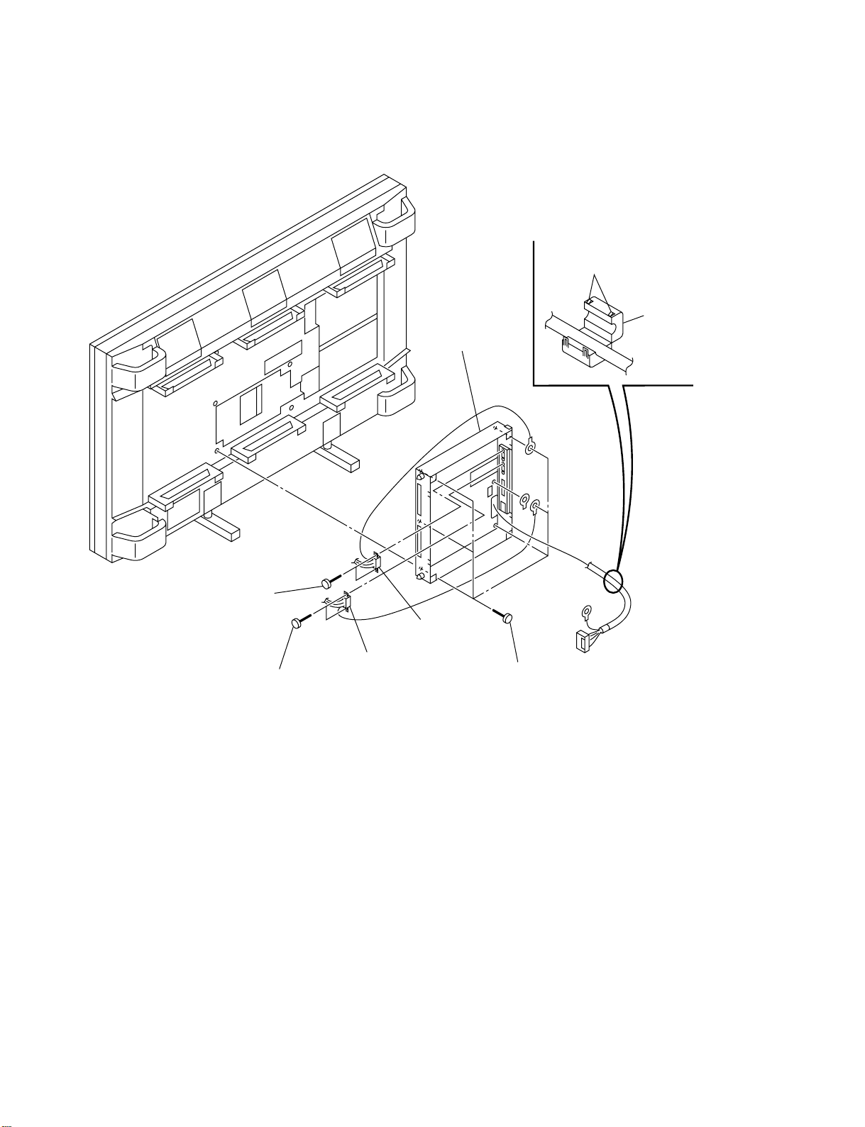
2-2-5. SC Block Removal
* Remove the B board. (Refer to 2-2-4.)
Two claws
5 Ferrite core
7 SC block
1 Two screws
(+PSW3 x 10)
3 Two screws
(+PSW3 x 10)
2 Connector assy
(8P)
4 Connector assy
(7P)
CN3
6 Six screws
(+PSW4 x 10)
2-6
PFM-500A3WE/500A3WG/500A3WU/510A2WE/510A2WG/510A2WU
Page 49
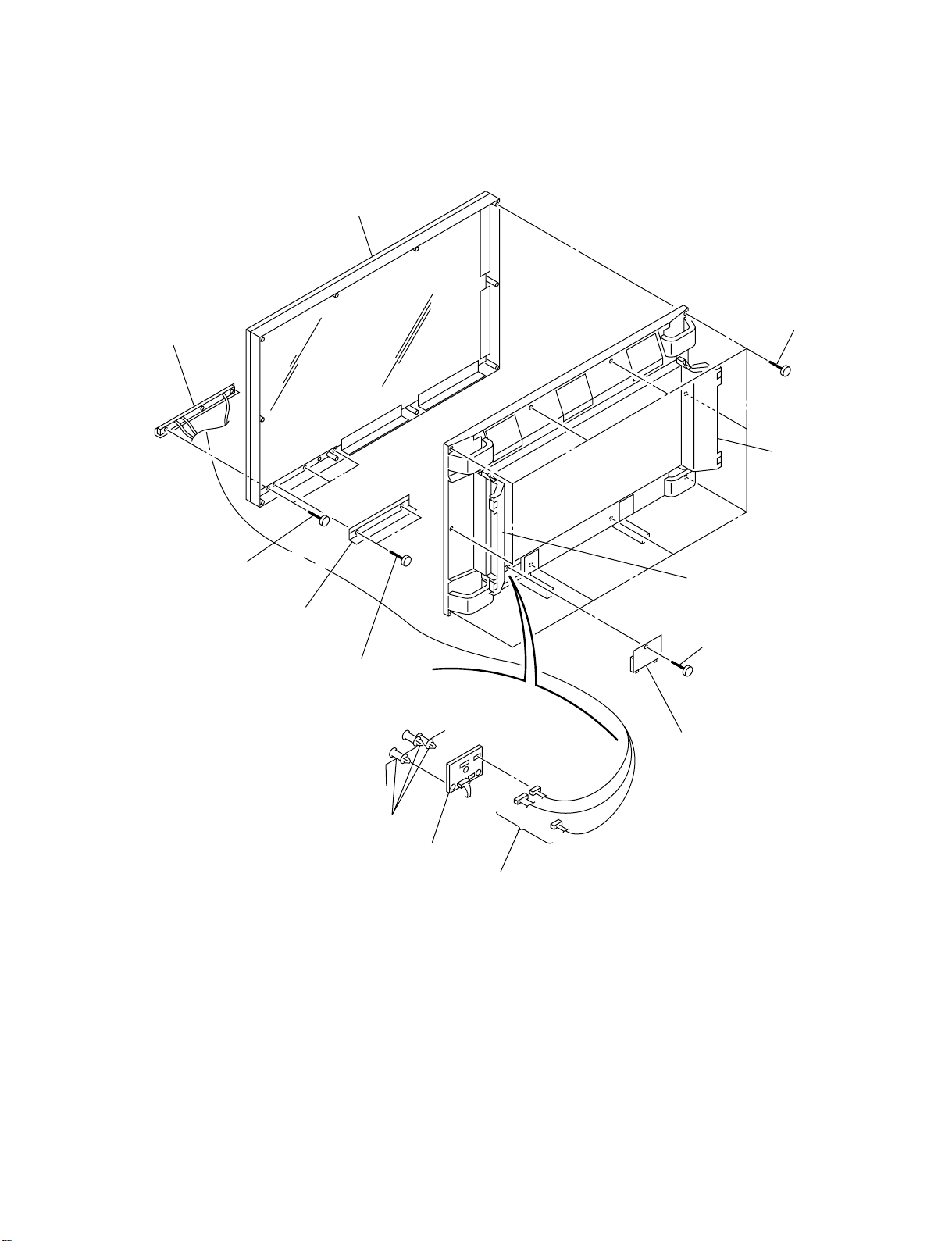
2-2-6. Bezel Assy and H6 Board Removal
* Open the side cover. (Refer to 2-2-1.)
5 Bezel assy
9 Key board unit
4 Ten screws
(+P4 x 16)
Side cover
8 Three screws
(+PSW3 x 10)
7 Filter bracket (H)
6 Two screws
(+PSW4 x 10)
0 Three PWB holders
!- H6 board
Side cover
1 Screw
(+PSW4 x 10)
2 Hand hole cover
CN703
CN704
CN702
3 Three connectors
PFM-500A3WE/500A3WG/500A3WU/510A2WE/510A2WG/510A2WU
2-7
Page 50
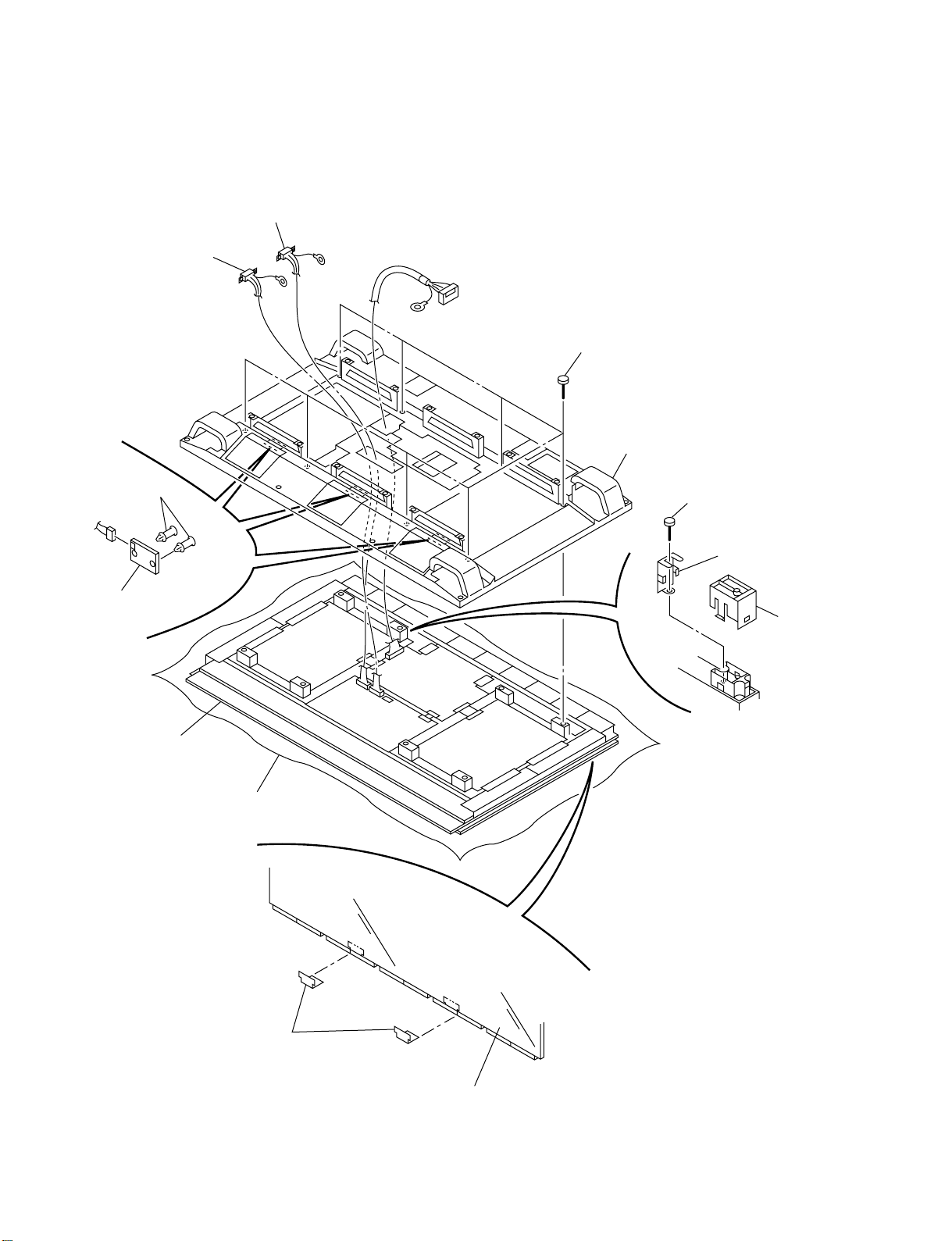
2-2-7. Plasma Display Panel and S1 Board Removal
y
* Remove the Bezel assy. (Refer to 2-2-6.)
* Remove the SC block. (Refer to 2-2-5.)
Connector assy (8P)
Connector assy (8P)
CN3
1 Eight screws
(+PSW5 x 50)
2 Rear cabinet assy
8 Two PWB holders
CN1201
9 S1 board
3 Plasma display
panel
5 Screw
(+PSW4 x 10)
6 Earth plate
4 Spacer
Cushion
2-8
7 Two protection plates
Plasma displa
panel
PFM-500A3WE/500A3WG/500A3WU/510A2WE/510A2WG/510A2WU
Page 51
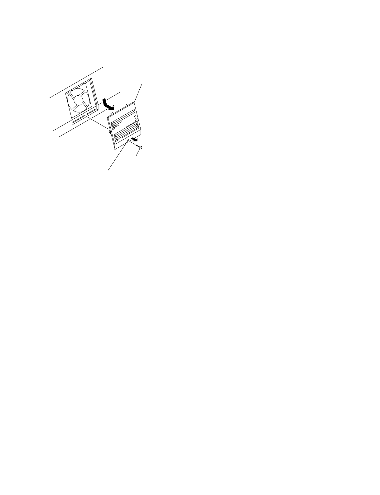
2-2-8. Fan Cover Removal
g
)
B
2 Pull
(Pull up with the tip of a screw
driver or somethin
3 Remove the fan cover
in the direction of the arrow B.
A
1 Screw
(+PSW4 x 10)
similar.
PFM-500A3WE/500A3WG/500A3WU/510A2WE/510A2WG/510A2WU
2-9
Page 52

Page 53
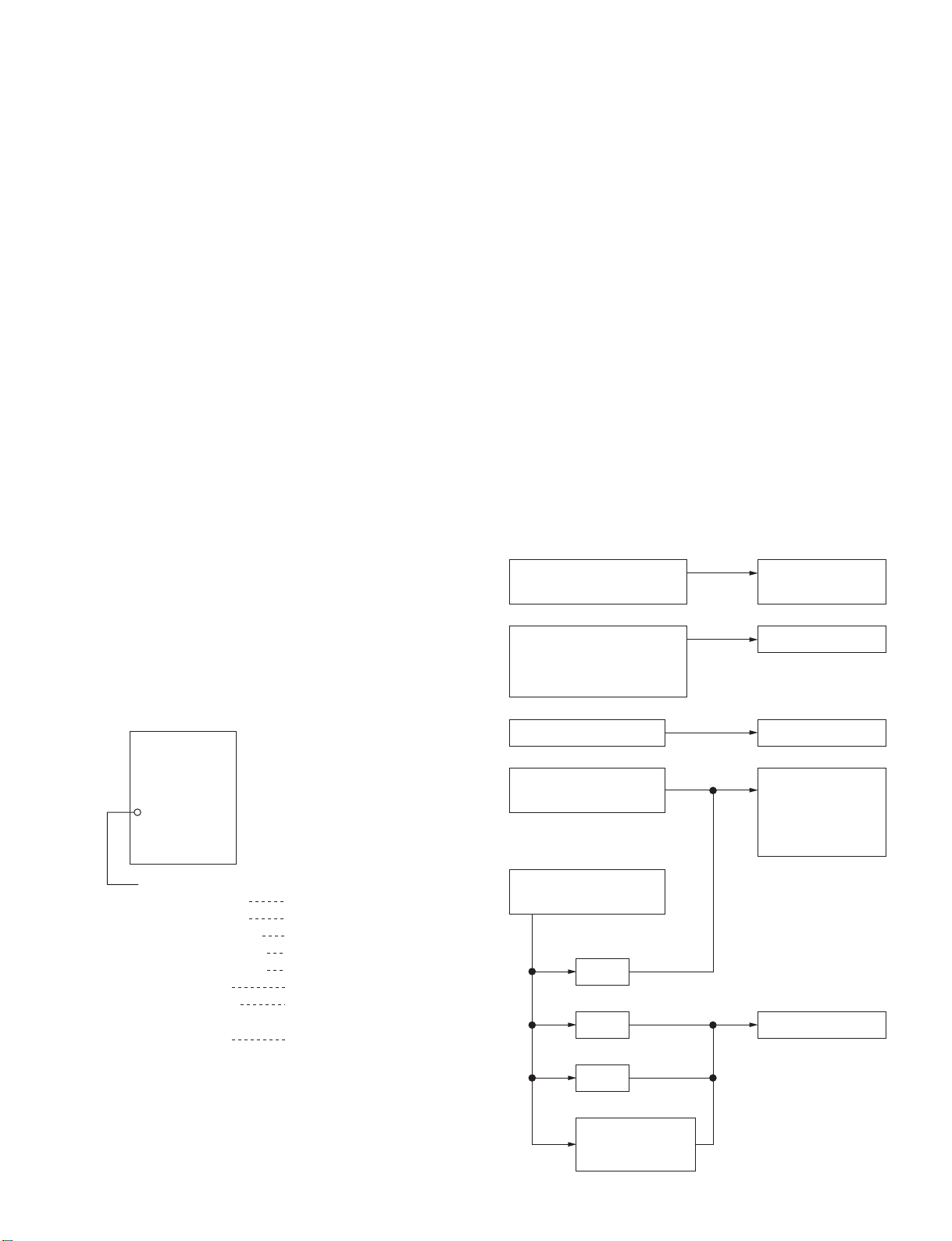
Section 3
Operation check only
When IC200 and its peripheral
parts (the parts that are
shown in schematic diagram
B (2/14) ) are replaced.
When PDP is replaced.
STATUS/TEST
B board
H6 board
Power supply board
(APS-136 M)
(APS-132 M)
When memory (IC511) on
the B board is replaced.
WHITE BALANCE
ADC CALIBRATION
ADC CALIBRATION
WHITE BALANCE
EEPROM RESET
WHITE BALANCE
ADC CALIBRATION
MAINTENANCE
STATUS/TEST
S1 board
When any of the following
boards is replaced.
When any repairs that
are related to picture quality
are performed.
Electrical Adjustments
3-1. Equipment Required
. Oscilloscope
Tektronix 2465 or equivalent
(band width : 350 MHz or more)
. VG (Programmable video signal generator)
VG814 or equivalent
. Frequency counter
Advantest TR5821AK or equivalent
. Digital voltmeter
Advantest TR6845 or equivalent
. Potential transformer
. Regulated DC power supply
. Remote commander (RM-921)
Note : Perform the following adjustments at least 5 minutes after turning on
the power.
3-2. Electrical Adjustments Using the
Service Mode
The electrical adjustments can be performed using the remote
commander RM-921 supplied with the PFM-500A3W/510A2W.
The remote commander has the Service Mode. Select the Service
Mode to perform the electrical adjustments as listed below.
rr
r Operation of remote commander in the
rr
Service Mode
The four keys of MENU, ENTER, SELECT+ and SELECT_ are the basic operation keys in the same manner as
in the user adjustment. The other keys can be operated in
the same manner as in the user adjustment.
Note : In the previous models PFM-500A1W/A2S and PFM-510A1W, the
electrical adjustments for service are performed using the numeric
keys. However, in this model, the electrical adjustments for service
are performed using the basic operation keys in the same manner as
in the user adjustment.
When the main power is turned on while the machine is in the
previous models, the OSD (on-screen display) appears automatically.
However, in this mode, the OSD appears when the MENU key is
pressed in the same manner as in the user menu.
rr
r The electrical adjustments using the Service
rr
Mode become necessary in the following
cases.
When any of the following repairs is performed, adjustment using the service mode becomes necessary.
rr
r Service Menu
rr
When you enter the Service Mode, the mode menu appears
as shown below. The mode menu contains the three menus
of MAIN MENU, SERVICE MENU and MANUAL
MENU as shown. Select the SERVICE MENU to perform
the electrical adjustments.
MODE SELECT
MAIN MENU
SERVICE MENU
MANUAL MENU
SERVICE MENU
EEPROM RESET
WHITE BALANCE
ADC CALIBRATION
VIDEO PROCESSOR
SPECIAL FUNCTION
PRESET EDIT
MAINTENANCE
STATUS/TEST
How to enter the Service Mode :
In the STAND-BY state, press the keys in the following order.
[DISPLAY] → [5] → [VOL+] → [POWER]
How to exit the Service Mode :
Turn off the main power once and back on to enter the STANDBY state or turn off the main power to exit the Service Mode.
PFM-500A3WE/500A3WG/500A3WU/510A2WE/510A2WG/510A2WU
: This is the user’s menu. Use the
MAIN MENU when user adjustment items
such as operation checks upon completion
of adjustments, are going to be made.
: This is the menu that is used for electrical
adjustments. This section of this manual
describes how to use the SERVICE MENU.
: This menu is used in production factory.
Do not make any attempts to use this menu
and do not make any operations using this menu.
Initialization of EEPROM
Gain adjustment of digital gamma circuit
Calibration of A/D converter
Level adjustment of video processor circuit
Setting the special functions
Editing the preset signals
Setting the data that are unique
to the particular machine
Internal status and function test
3-1
Page 54
SERVICE MENU
1. EEPROM RESET
EEPROM Configuration
Table 1 shows the configuration of EEPROM. The entire
area or the respective areas of the EEPROM can be
separately initialized.
Menu Structure
Select the desired area of EEPROM to be initialized using
the following menu.
EEPROM RESET
WHOLE AREA
COMMON
COLOR TEMP
PROG. PRESET
FIXED PRESET
LAST MEMORY
USER MEMORY
FACTORY
To initialize the desired area, firstly select the desired item
from the EEPROM RESET menu. Change the selected
item from CANCEL to EXECUTE. Then press ENTER.
e) FIXED PRESET
Only the FIXED PRESET area of the EEPROM as
shown in Table 1 is initialized.
When the FIXED PRESET area is initialized, the basic
preset area is initialized to the built-in standard value
that is stored in the system controller.
f) LAST MEMORY
Only the LAST MEMORY area of the EEPROM as
shown in Table 1 is initialized.
When the LAST MEMORY area is initialized, only
the last memory data of every signal that is adjusted by
user is initialized.
g) USER MEMORY
Only the USER MEMORY area of the EEPROM as
shown in Table 1 is initialized.
When the USER MEMORY area is initialized, all of
the 20 types of adjustment data that is saved by the
MEMORY function of the user menu are initialized to
EMPTY.
h) FACTORY
Only the FACTORY area of the EEPROM as shown
in Table 1 is initialized.
When the FACTORY area is initialized, all areas of
the MEMORY except the areas that are listed below
are initialized.
a) WHOLE AREA
The entire area of the EEPROM is initialized. Initializing the entire area of the EEPROM has the same result
as all menu items of COMMON, COLOR TEMP,
PROG. PRESET, FIXED PRESET, LAST MEMORY,
USER MEMORY and FACTORY are executed.
b) COMMON
Only the COMMON area of the EEPROM as shown in
Table 1 is initialized.
When the COMMON area is initialized, the data that is
unique to the particular machine and the common data
(CONFIG MENU, REMOTE MENU) are initialized.
c) COLOR TEMP
Only the COLOR TEMP area of the EEPROM as
shown in Table 1 is initialized.
When the COLOR TEMP area is initialized, the color
temperature data in HIGH, LOW and the user setup
data from 1 to 6 are initialized to 255. The users
names are also initialized to “1” to “6”.
d) PROG. PRESET
Only the PROG. PRESET area of the EEPROM as
shown in Table 1 is initialized.
When the PROG. PRESET area is initialized, the
preset area (for 20 types) that is reserved as spare is
initialized.
3-2
Items that are not initialized by the “FACTORY” RESET
function.
..
. EEPROM ID CODE
..
..
. INDEX NUMBER
..
..
. MODEL NAME
..
..
. SERIAL NUMBER
..
..
. AUDO DIGITAL
..
..
. DIGITAL TYPE
..
..
. YUV2 TYPE
..
..
. AUTO PLL SETUP
..
..
. AUTO PLL PIXEL
..
..
. H/V SHIFT
..
..
. VIDEO SHARP SW
..
..
. AUTO FT CANCEL
..
..
. WATCH ERROR
..
..
. Y GAIN
..
..
. R-Y GAIN
..
..
. B-Y GAIN
..
..
. R CUTOFF
..
..
. B CUTOFF
..
..
. ADC R GAIN
..
..
. ADC G GAIN
..
..
. ADC B GAIN
..
..
. ADC R OFFSET
..
..
. ADC G OFFSET
..
..
. ADC B OFFSET
..
PFM-500A3WE/500A3WG/500A3WU/510A2WE/510A2WG/510A2WU
Page 55
2. WHITE BALANCE
3. ADC CALIBRATION
Menu Structure
Adjust the white balance of the desired color temperature
by selecting the items of the WHITE BALANCE menu
and by adjusting the R, G, B gain of the digital gamma
circuit.
WHITE BALANCE
WINDOW
COLOR TEMP
RED GAIN
GREEN GAIN
BLUE GAIN
: OFF
: HIGH
: 255
: 255
: 255
a) WINDOW
The PFM-500A3W/510A2W has the built-in window
signal for white balance adjustment. There are two
sizes that are the large and small windows. Select the
optimum size of window for white balance adjustment.
OFF : Window does not appear.
TYPE1 : Small window
TYPE2 : Large widow
Note : When white balance is going to be adjusted using an external signal,
perform the A/D converter calibration (referring to the next paragraph
3) ADC CALIBRATION) before starting the white balance adjustment.
b) COLOR TEMP
To adjust the white balance, firstly select the desired
color temperature from HIGH, LOW, 1, 2, 3, 4, 5 or 6
on the COLOR TEMP sub-menu. Color temperature
of items 1 to 6 are the same as those of the user menu.
c) RED GAIN
Adjust the red gain of the selected color temperature.
The range of adjustment is from 010 to 255.
d) GREEN GAIN
Adjust the green gain of the selected color temperature.
The range of adjustment is from 010 to 255.
e) BLUE GAIN
Adjust the red blue of the selected color temperature.
The range of adjustment is from 010 to 255.
Menu Structure
Calibrate the A/D converter (IC200) until non-uniformity between
the R, G and B channels of the A/D converter is removed.
ADC CALIBRATION
AUTO
CAL MODE
RED GAIN
GREEN GAIN
BLUE GAIN
RED BIAS
GREEN BIAS
BLUE BIAS
R : – – – G : – – – B : – – –
: OFF
: 128
: 128
: 128
: 128
: 128
: 128
: 128
a) AUTO
The A/D converter is automatically calibrated.
Note : When sufficient adjustment accuracy cannot be obtained by the
automatic calibration, perform basically the manual calibration using
the following ADC CALIBRATION menu items.
b) CAL MODE
The A/D converter has the calibration mode as its operating mode as follows.
* The A/D converter has the R, G, B GAIN adjust-
ments and the R, G, B BIAS adjustments. The
GAIN adjustments of the A/D converter are used for
CONTRAST adjustment in the machine. The R, G,
B BIAS adjustments of the A/D converter are used
for BRIGHTNESS adjustment in the machine.
CAL MODE - OFF : Standard display state
The R, G, B GAIN values and the R, G, B BIAS values are
controlled by the CONTRAST/BRIGHT data of the user
menu. The R, G, B GAIN values and the R, G, B BIAS
values of this menu cannot be adjusted independently.
CAL MODE - OFF : Calibration mode
The R, G, B GAIN values and the R, G, B BIAS values
of this menu can be adjusted independently. The R, G,
B data that appear in the most-bottom part of the menu
in cyan, change from the indication “___” to the indication of any digital output data of the A/D converter.
c) RED GAIN/GREEN GAIN/BLUE GAIN
The respective R, G, B GAIN values can be adjusted
independently.
The range of adjustment is from 000 to 255.
White Balance Adjustment
Refer to section “3-3. White Balance Adjustment”.
PFM-500A3WE/500A3WG/500A3WU/510A2WE/510A2WG/510A2WU
d) RED BIAS/GREEN BIAS/BLUE BIAS
The respective R, G, B BIAS values can be adjusted
independently.
The range of adjustment is from 000 to 255.
A/D Calibration Adjustment
Refer to section “3-4. A/D Calibration Adjustment”.
3-3
Page 56
4. VIDEO PROCESSOR
5. SPECIAL FUNCTION
Menu Structure
The following items of the video processor can be adjusted
using this menu. However, all items of the video processor
have the default values on which normal operations are performed. Therefore, the video processor normally needs no
adjustment.
VIDEO PROCESSOR
Y GAIN
R-Y GAIN
B-Y GAIN
RED CUTOFF
BLUE CUTOFF
: 111
: 082
: 128
: 143
: 100
a) Y GAIN
The range of adjustment is from 000 to 255.
Default value : 111
b) R-Y GAIN
The range of adjustment is from 000 to 255.
Default value : 082
c) B-Y GAIN
The range of adjustment is from 000 to 255.
Default value : 128
d) RED CUTOFF
The range of adjustment is from 000 to 255.
Default value : 143
e) BLUE CUTOFF
The range of adjustment is from 000 to 255.
Default value : 100
Video Processor Adjustment
Refer to section “3-5. Video Processor Adjustment”.
(Perform the service menu adjustment of the video processor only when the specifications cannot be satisfied by section “3-5. Video Processor Adjustment”.)
Menu Structure
Various special functions as listed in the SPECIAL
FUNCTION menu can be independently set as required.
SPECIAL FUNCTION
AUTO DIGITAL
DIGITAL TYPE
RGB2 TYPE
AUTO PLL SETUP
AUTO PLL PIXEL
H/V SHIFT
VIDEO SHARP SW
AUTO FT CANCEL
a) AUTO DIGITAL
Sets enable/disable of automatic switching of the
DIGITAL IN terminal.
The PFM-500A3W/510A2W is equipped with the
DIGITAL IN terminal (CN2: Pins A21 to A32/B21 to
B32) using the LVDS. The automatic switching of the
DIGITAL IN terminal can be enabled/disabled as
follows by the setup of the AUTO DIGITAL item of
this menu.
ON : When the AUTO DIGITAL is set to ON,
connect pin-A20 to GND to switch the DIGI-
TAL IN terminal to the digital input. Discon-
nect pin-A20 to open to switch the DIGITAL
IN terminal to the input state before the
terminal is switched to digital.
OFF : When the AUTO DIGITAL is set to ON, the
automatic switching of the DIGITAL IN
terminal is disabled.
Set the AUTO DIGITAL item to the ON position
normally.
b) DIGITAL TYPE
Selects either RGB signal or the YUV signal as the
input signal to the DIGITAL IN terminal.
RGB : The RGB signal is selected as the input signal
to the DIGITAL IN terminal.
YUV : The YUV signal is selected as the input signal
to the DIGITAL IN terminal.
Set the DIGITAL TYPE item to the RGB position
normally.
3-4
c) RGB2 TYPE
Selects either RGB signal or the YUV signal as the
input signal to the RGB2 terminal.
RGB : The RGB signal is selected as the input signal
to the RGB2 terminal.
YUV : The YUV signal is selected as the input signal
to the RGB2 terminal.
Set the RGB2 item to the RGB position normally.
PFM-500A3WE/500A3WG/500A3WU/510A2WE/510A2WG/510A2WU
Page 57

d) AUTO PLL SETUP
Sets enable/disable of automatic execution of the
PIXEL ADJUST function.
ON : When the AUTO PLL SETUP is set to ON, the
PIXEL ADJUST is automatically executed
when the main power is turned on or when the
input signal is switched. (Be noted that about
10 seconds are required to output the video
signal after switching the input signal when this
function is kept to the ON position.)
OFF : The automatic PIXEL ADJUST is executed
only when AUTO item of the user menu
PIXEL ADJUST is activated.
This function becomes valid only when the signal that
enables the PIXEL ADJUST is inputted to the PFM500A3W/510A2W.
Set the AUTO PLL SETUP item to the OFF position
normally.
g) VIDEO SHARP SW
Sets analog aperture ON or OFF.
The two methods are used for the aperture correction
of the video signals (NTSC/PAL/SECAM/NTSC4.43/
PAL60 and YUV signal having horizontal frequency
of 15 kHz). These two methods are the scaling filter
and the analog aperture of the scan converter.
ON : Both the scaling filter and the analog aperture
of the scan converter are used for aperture
correction.
OFF : Only the scaling of the scan converter is used
for aperture correction.
This function becomes valid only when the signal
(NTSC/PAL/SECAM/NTSC4.43/PAL60 and YUV
signal having horizontal frequency of 15 kHz) is
inputted to the PFM-500A3W/510A2W.
Set the VIDEO SHARP SW item to the ON position
normally.
e) AUTO PLL PIXEL
Selects the functions that are automatically adjusted
when PIXEL ADJUST is executed.
ON : Both the TOTAL H PIXEL and DOT PHASE
are automatically adjusted.
OFF : Only the DOT PHASE is automatically
adjusted.
In the case that the PFM-500A3W/510A2W is used
under the environment where input signal contains
much noise, there are cases that the PIXEL ADJUST
mis-operations. Therefore, set the AUTO PLL PIXEL
to the OFF position. In such a case, the TOTAL H
PIXEL can be adjusted only manually.
This function becomes valid only when the signal that
enables the PIXEL ADJUST is inputted to the PFM500A3W/510A2W.
Set the AUTO PLL PIXEL item to the ON position
normally.
f) H/V SHIFT
Selects the method to control the horizontal and
vertical picture shift.
EDGE : When EDGE is selected, a picture is shifted
by changing the starting position when
reading data into memory. Using this
function, the entire area including blanking of
all pictures can be displayed by shifting. The
variable range of shifting is 1 horizontal and
vertical period respectively.
CAPT : When CAPT is selected, the picture that is
already written into memory is shifted by a
scan converter. Using this function, a picture
can be shifted as much as ± 50 % of a
picture. When a picture is partly lacked at an
end of a picture, the lacked portion of a
picture cannot be displayed.
Set the H/V SHIFT item to the EDGE position normally.
PFM-500A3WE/500A3WG/500A3WU/510A2WE/510A2WG/510A2WU
h) AUTO FT CANCEL
Sets the FT (field tearing) cancel circuit ON or OFF.
The PFM-500A3W/510A2W has the FT (field tearing)
prevention circuit caused by the overrun of memory
while it is displaying the moving picture (video and
DTV). However, there can be cases that noise appears
on screen when the FT (field tearing) prevention is
being executed.
ON : The FT (field tearing) is cancelled in every
picture size and in every shift conditions as
long as the PFM-500A3W/510A2W is
receiving the moving picture. When this item
is set to ON, noise may appear only once
after the size/shift is adjusted. (Noise does
not last long but appears only once when the
size/shift adjustment is complete.)
OFF : The FT (field tearing) cancel circuit is
disabled. When OFF is selected, there can be
a case that the FT (field tearing) appears on
screen depending on the adjustment conditions of picture size/shift. However, the noise
due to operation of the processing circuit
does not occur.
Set the AUTO FT CANCEL item to the ON position
normally.
3-5
Page 58
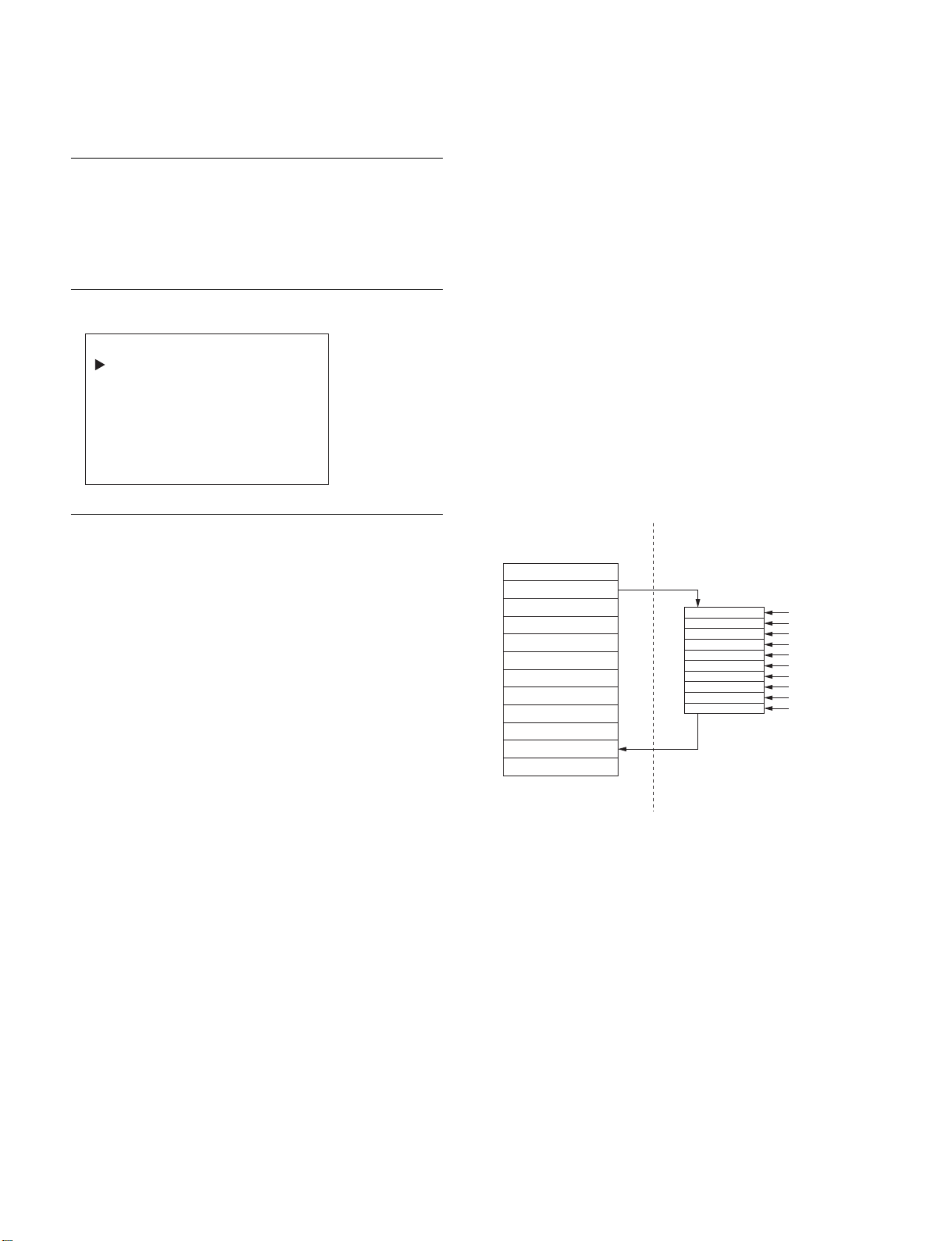
6. PRESET EDIT
Preset Data Configuration
Memory map of the preset data area is shown in Table 1
(PROG. PRESET/FIXED PRESET). The areas from 1 to
20 are assigned to store the additional signal. The areas
from 21 to 74 are assigned to store the internal signal.
Menu Structure
PRESET EDIT
ORIGINAL DATA SELECT
DATA EDIT
SAVE AREA SELECT
How To Edit The Preset Data
As shown in the illustration, the system controller contains
the memory area (i.e., Editing RAM) that is assigned only
for data editing. The source data that is used for editing
must be firstly copied to the Editing RAM. Edit then the
copied data as desired. Finally save the result of editing in
the specified preset area of the EEPROM.
(The illustration shows an example that the data in the
preset area No. 02 is once copied to the Editing RAM
where data is edited. The edited data is sent back to the
preset area No. 11 where the edited data is saved.)
EEPROM Preset areas System controller
Preset Area 01
Preset Area 02
Preset Area 03
Preset Area 04
Preset Area 05
Preset Area 06
Preset Area 07
Preset Area 08
Preset Area 09
Preset Area 10
Preset Area 11
Preset Area 12
Editing RAM
Editing
3-6
PFM-500A3WE/500A3WG/500A3WU/510A2WE/510A2WG/510A2WU
Page 59
a) ORIGINAL DATA SELECT
Menu Structure
Select the source data that is used for editing. Then the selected source data is
copied to the Editing RAM.
ORIGINAL DATA SELECT
CURRENT DATA SELECT
FORMAT TABLE
- ORIGINAL FORMAT H FREQUENCY
V FREQUENCY
SYNC POL (H/V)
: PROGRAM1
: 31.47 [kHz]
: 60.00 [Hz]
: NEGE/NEGA
(1) The signal that is being inputted at present
is selected as the source data.
(2) The signal that is already stored in the preset
area is selected as the source data.
(3) Frequency of the signal that is selected
as the source data is displayed.
EDIT MODE
: DIRECT
(4) Type of the signal that is selected as the
source data is displayed.
(1) CURRENT DATA SELECT
When an editing is performed using the signal that is being inputted at present is
selected as the source data, move the cursor to this item and press ENTER. The
selected data is copied to the Editing RAM.
(2) FORMAT TABLE : PROGRAM 1
When an editing is performed using the signal that is already stored in the preset
area is selected as the source data, move the cursor to this item and press
ENTER. Select the desired area from Table 1 by pressing the +/_ keys. The
selected data is copied to the Editing RAM.
(3) - ORIGINAL FORMAT -
Frequency of the signal that is selected as the source data in step (1) or (2) is
displayed.
Use the frequency data as the fundamental information when selecting a source
data.
(4) EDIT MODE
When the signal that is being inputted at present is selected as the source data,
the message DIRECT appears. When the signal that is already stored in the
preset area is selected as the source data, the message TABLE appears.
Note : The editing items that can be editing here are different in the DIRECT mode and the TABLE mode.
Refer to the next sub-section “b) DATA EDIT” for the editing items.
< When DIRECT mode is used for editing >
… The DIRECT mode is used when editing is performed while watching the
picture on screen in the case that the specifications of the signal are not known. …
When DIRECT mode is selected, select the desired adjustment item referring to
the next sub-section “b) DATA EDIT” by pressing the +/_ keys. Press the ENTER key. Then the result of data adjustment is reflected on the display screen.
(Pressing the MENU key returns to the previous menu display.)
However, the three adjustment items H FREQUENCY, V FREQUENCY and
SYNC POL cannot be changed by the menu operation.
< When TABLE mode is used for editing >
… The TABLE mode is used when the specifications of the signal to edit are
already known. …
All adjustment items adjusted by the menu but result of adjustment is not
reflected on the actual picture. Data can be edited only.
PFM-500A3WE/500A3WG/500A3WU/510A2WE/510A2WG/510A2WU
3-7
Page 60
b) DATA EDIT
Menu Structure
The following items of the source data that is copied to the Editing RAM can be
modified as described below.
DATA EDIT
INPUT SELECT
H FREQUENCY
V FREQUENCY
SYNC POL (H/V)
TOTAL H PIXEL
LEFT EDGE
H RESOLUTION
TOP EDGE
V RESOLUTION
DOT PHASE
CP PLACEMENT
CP DURATION
INTERLACE MODE
FILED MODE
FRAMELOCK MODE
MATRIX SELECT
PICTURE AGC
ASPECT
ZOOM
APERTURE INIT
APERTURE HIGH
APERTURE MID
APERTURE LOW
AUTO PLL
SYNC WIDTH (µs)
: 1100000
: 31.47 [kHz]
: 60.00 [Hz]
: NEGA/NEGA
: 800
: 140
: 640
: 35
: 480
: 128
: 005
: 016
: OFF
: OFF
: OFF
: ITU709
: ON
: 4 × 3
: × 1
: MID
: 000
: 002
: 004
: ON
: 003.81
(1) Acceptable type of input signal
(2) Horizontal frequency
(3) Vertical frequency
(4) Sync signal polarity
(5) Total number of horizontal dots
(6) Horizontal dot position to start reading
(7) Horizontal resolution (Number of dots)
(8) Vertical dot position to start reading
(9) Vertical resolution (Number of dots)
(10) Dot phase
(11) Clamp pulse width (Number of dots)
(12) Clamp pulse position (Number of dots)
(13) Interlace setting
(14) In-field processing setting
(15) Vertical sync setting
(16) Color difference matrix setting
(17) Automatic brightness adjustment setting
(18) Aspect ratio setting
(19) Zoom setting
(20) Aperture initial value setting
(21) Aperture data setting
(22) Aperture data setting
(23) Aperture data setting
(24) Automatic PIXEL ADJUST setting
(25) Horizontal sync signal width
Note : A maximum of 8 lines of the above menu can be displayed on screen. The other menu items can be
displayed by scrolling the display by moving the cursor up or down.
3-8
PFM-500A3WE/500A3WG/500A3WU/510A2WE/510A2WG/510A2WU
Page 61

(1) INPUT SELECT
The input signals that are acceptable to the PFM500A3W/510A2W are set.
This item consists of 8 bits. Each bit corresponds to
each type of input signal. Only the input channel to
which “1” is set, can be received by the PFM500A3W/510A2W.
INPUT SELECT : 1 1 0 0 0 0 1
RGB1
RGB2
YUV1
YUV2
LINE
Y/C
DIG
Note : Regarding the LINE and Y/C input channels, these signals having
horizontal frequency of 15 kHz can be inputted. Because these input
signals pass through the double-speed processing circuit in the PFM500A3W/510A2W circuit configuration, do not use the LINE and Y/C
input channels.
(2) H FREQUENCY
The horizontal frequency is set.
Note: This menu item cannot be modified in the DIRECT mode because the
DIRECT mode can edit the signal that is being inputted at present.
(3) V FREQUENCY
The vertical frequency is set.
Note : This menu item cannot be modified in the DIRECT mode because
the DIRECT mode can edit the signal that is being inputted at
present.
(4) SYNC POL (H/V)
Polarity of sync signal is set.
SYNC POL (H/V) : NEGA/NEGA
Horizontal sync polarity
Vertical sync polarity
To set the polarity, select as follows:
Negative polarity : NEGA
Positive polarity : POSI
SOG : ___
Note : This menu item cannot be modified in the DIRECT mode because
the DIRECT mode can edit the signal that is being inputted at
present.
(5) TOTAL H PIXEL
The total number of dots in a horizontal period is set.
The number of dots that is set here becomes the initial
value of the user menu “TOTAL H PIXEL”.
Note : Set the total number of dots to satisfy the following conditions.
TOTAL H PIXEL > [LEFT EDGE + H RESOLUTION]
(6) LEFT EDGE
The horizontal sync width (in dots) + horizontal back
porch width (in dots) are set.
(7) H RESOLUTION
Horizontal resolution power is set.
Note : When 1280 or more is set to the horizontal resolution, picture may
not be displayed normally on screen. When a signal that has the
higher resolution than the SXGA signal, is going to be preset, reduce
the number of horizontal resolution by skipping or any other means
down to 1280 or less.
(8) TOP EDGE
The vertical sync width (in lines) + vertical back porch
width (in lines) are set.
Note : Set the TOP EDGE value to satisfy the following conditions.
[TOP EDGE + V RESOLUTION] < [horizontal frequency + vertical
frequency]
(9) V RESOLUTION
The vertical resolution is set.
Note : Set the V RESOLUTION value to satisfy the following conditions.
[TOP EDGE + V RESOLUTION] < [horizontal frequency + vertical
frequency]
(10)DOT PHASE
Pulse phase of the horizontal sampling frequency is
set.
The pulse phase that is set here becomes the initial
value of DOT PHASE of the user menu.
The pulse phase can be set in the range of 000 to 255.
(11)CP PLACEMENT
Clamp pulse position is set.
The clamp pulse position is set starting from the
trailing edge of horizontal sync signal (when data is
000). Increasing this value moves the clamp pulse in
the direction toward the picture area.
The clamp pulse generating position “Tcp” is given by
the following equation starting from the trailing edge
of horizontal sync signal.
Tcp = CP PLACEMENT / [horizontal sync frequency
x TOTAL H PIXEL] (in seconds)
(12)CP DURATION
Clamp pulse width is set.
The clamp pulse width is set starting from the position
that is determined by CP PLACEMENT. Increasing
this value widens the clamp pulse width in the direction toward the picture area.
The clamp pulse width “Wcp” is given by the following.
Wcp = CP DURATION / [horizontal sync frequency x
TOTAL H PIXEL] (in seconds)
PFM-500A3WE/500A3WG/500A3WU/510A2WE/510A2WG/510A2WU
3-9
Page 62

(13)INTERLACE MODE
Whether the input signal is interlaced or not is set.
ON : When the input signal is the interlaced signal.
OFF : When the input signal is not the interlaced
signal.
(14)FIELD MODE
Whether the interlaced signal is processed within a
field or within a frame, is set.
ON : When the input interlaced signal is processed
within a field.
OFF : When the interlaced signal is processed within
a frame.
Select the ON position when a signal has a low corelationship between the two fields within a frame
such as moving picture.
(20)APERTURE INIT
The desired aperture is selected from HIGH or MID or
LOW. Result of this setting becomes the initial value
of the user menu APERTURE.
(21)APERTURE HIGH
The scaling filter value when selecting HIGH of the
APERTURE, is set. The scaling filter value can be set
in the range of 000 to 011. (Refer to the Supplement
to APERTURE in the following paragraph.)
(22)APERTURE MID
The scaling filter value when selecting MID of the
APERTURE, is set. The scaling filter value can be set
in the range of 000 to 011. (Refer to the Supplement
to APERTURE in the following paragraph.)
(15)FRAMELOCK MODE
Whether the PDP display picture is synchronized with
the input signal to scan converter or not, is set.
ON : The PDP display picture is synchronized with
the input signal.
OFF : The PDP display picture is asynchronous with
the input signal.
When moving picture (animation) is going be displayed, select the ON position.
Note : This item can be set to ON as long as the vertical frequency of the
input signal is in the range of 50 to 60 Hz.
(16)MATRIX SELECT
The color difference matrix when the YUV signal is
being input, is set.
(17)PICTURE AGC
Whether the PICTURE AGC is turned ON or OFF is
set.
Result of this setting becomes the initial value of the
user menu PICTURE AGC.
This function becomes valid only when the COMPOSITE/YC/YUV signal is being received.
(18)ASPECT
The desired aspect ratio is selected from the aspect
ratios of 4 x 3 or 16 x 9 or W ZOOM. Result of this
setting becomes the initial value of the user menu
ASPECT.
Note : The W ZOOM can not be selected when the ZOOM is in the range of
x 2 to x 4.
(23)APERTURE LOW
The scaling filter value when selecting LOW of the
APERTURE, is set. The scaling filter value can be set
in the range of 000 to 011. (Refer to the Supplement
to APERTURE in the following paragraph.)
< Supplement to APERTURE >
The PFM-500A3W/510A2W has the 12 different types of
built-in scaling filter. Select an appropriate filter using the
following filter characteristics chart as a guideline.
Wide
(Sharp)
Frequency
bandwidth
Narrow
(Soft)
012345678910
11
(19)ZOOM
The desired zoom ratio is selected from the zoom
ratios of x 1 or x 2 or x 3 or x 4. Result of this
setting becomes the initial value of the user menu
ZOOM.
Note : Any zoom ratios other than x 1 cannot be selected when the
ASPECT is W ZOOM.
3-10
PFM-500A3WE/500A3WG/500A3WU/510A2WE/510A2WG/510A2WU
Page 63
(24)AUTO PLL
Whether the user menu adjustment PIXEL ADJUST is
enabled or disabled, is set.
ON : The user menu adjustment PIXEL ADJUST is
enabled.
OFF : All items of the adjustment PIXEL ADJUST
show the indication [___]. The user menu
adjustment PIXEL ADJUST is disabled.
Select the OFF position when the setup of the TOTAL
H and that of RESOLUTION do not agree with
specifications of the actual input signal.
(25)SYND WIDTH (µs)
Sync pulse width of the horizontal sync signal is set in
units of microseconds [µseconds].
This menu item is prepared for the purpose of stabilization of the sync signal separation circuit. Therefore,
accurate setting is not necessarily needed.
If the sync signal width is not known, select “Not set”
(source data).
7. MAINTENANCE
Menu Structure
The data that is unique to the particular machine of the
PFM-500A3W/510A2W and the scan converter can be
upgraded using this menu.
MAINTENANCE
WATCH ERROR
MODEL NAME
SERIAL No.
SC PROG LOAD
a) WATCH ERROR
Errors of the built-in watch IC can be corrected.
To correct the error, enter the measurement value of
the frequency counter that is connected.
Range of adjustment is from 32761.85 Hz to 32774.25
Hz.
c) SAVE AREA SELECT
Menu Structure
The data that is copied in the Editing RAM, is saved in the
preset area.
SAVE AREA SELECT
SAVE AREA
DATA SAVE
: PROGRAM1
(1) Select the
desired preset
area to which
the data is saved.
(2) Execute to
save the data.
(1) SAVE AREA SELECT
Select the desired preset area from Table 1 to which
the content of the Editing RAM is saved.
(2) DATA SAVE
Execute to save the data to the preset area that is
selected by the SAVE AREA SELECT. Change the
item from CANCEL to EXECUTE. Then press
ENTER.
b) MODEL NAME
Model name can be set.
c) SERIAL No.
Serial number can be set.
d) SC PROG LOAD
The built-in program of the scan converter can be
modified using this menu item.
Change the item from CANCEL to EXECUTE. Then
press ENTER.
Watch Error Adjustment
Refer to section “3-6. Watch Error Adjustment”.
Note : Judgment whether the input signal agrees with the preset data or not,
is performed using the horizontal sync frequency, vertical sync
frequency and polarity of the sync signals. If the same sync signal
already exists in the preset area (Table 1), the specification that has
the small preset No., has a higher priority.
PFM-500A3WE/500A3WG/500A3WU/510A2WE/510A2WG/510A2WU
3-11
Page 64
8. STATUS/TEST
b) POWER SUPPLY
Menu Structure
The internal status of the PFM-500A3W/510A2W can be
checked and its functions can be checked using the STATUS/TEST menu.
STATUS/TEST
SIGNAL/SYNC
POWER SUPPLY
TEMPERATURE
FAN
SOFTWARE VERSION
TEST FUNCTION
a) SIGNAL/SYNC
SIGNAL/SYNC
H FREQUENCY
V FREQUENCY
FORMAT
SYNC POL (H/V)
STABLE
INSECURE
NO SYNC
: 31.47 [kHz]
: 60.00 [Hz]
: 640 x 480/60
: NEGA/NEGA
Horizontal frequency
Vertical frequency
Specifications of
the signal
Polarity of sync signal
Status of sync signal
Information regarding the sync signal of the input
signal is displayed.
Horizontal frequency :
Horizontal frequency of the input signal is displayed in
four digits.
Vertical frequency :
Vertical frequency of the input signal is displayed in
four digits.
Specifications of the signal :
Names of presets of the preset areas (Table 1) corresponding to input signal are displayed.
Polarity of sync signal :
Polarity of sync signal is displayed.
Status of sync signal :
Status of sync signal is displayed in cyan.
STABLE : Sync signal is stable.
INSECURE : Sync signal is unstable.
NO SYNC : Sync signal does not exist.
POWER SUPPLY
PDP VS (HV)
PDP VA (MV)
DIGITAL 5V
: 160 [V]
: 060 [V]
: 4.9 [V]
PDP drive voltage VS
PDP drive voltage VA
5 V power for
digital circuitry
The main DC power voltages of the PFM-500A3W/
510A2W are displayed.
PDP drive voltage VS :
High voltage power to PDP is displayed.
PDP drive voltage VA :
Medium voltage power to PDP is displayed.
5 V power for digital circuitry :
Internal 5 V power is displayed.
c) TEMPERATURE
TEMPERATURE
PANEL BACK SIDE
• P/S BLOCK SIDE
• CENTER
• I/O BLOCK SIDE
P/S INTERNAL
AMBIENT TEMP
: 25 [°C]
: 25 [°C]
: 25 [°C]
: OK
: 25 [°C]
Temperature at the
top on the rear of the
power supply panel
Power supply
internal temperature
information
Outside ambient
temperature
Internal temperature information of PFM-500A3W/
510A2W is displayed.
Temperature at the top on the
rear of the power supply panel :
Temperatures under the respective fans on the rear of
the power supply panel are displayed as follows.
P/S BLOCK SIDE :
Temperature of the side of the power supply block.
CENTER : Temperature at the center.
I/O BLOCK SIDE :
Temperature of the I/O terminal block.
Power supply internal temperature information :
Temperature status inside the power supply block is
displayed. The message OK appears when temperature is normal. The message NG appears when
temperature is abnormal.
Outside ambient temperature :
Temperature in the lower part (H6 board block) on the
rear of the PFM-500A3W/510A2W is displayed.
3-12
PFM-500A3WE/500A3WG/500A3WU/510A2WE/510A2WG/510A2WU
Page 65

d) FAN
f) TEST FUNCTION
FAN
PANEL BACK SIDE
• I/O BLOCK SIDE
• CENTER
• P/S BLOCK SIDE
POWER SUPPLY SIDE
• No. 1
• No. 2
DRIVE CIRCUIT
: OK
: OK
: OK
: OK
: OK
: OK
Fan at the top on
the rear of the
power supply panel
Power supply
internal fan
Fan drive circuit
The cooling fan operational information inside the
PFM-500A3W/510A2W is displayed. The message
OK appears when fan is normal. The message NG
appears when fan is abnormal.
Fan at the top on the rear of the power supply panel :
Operating states of the respective fans on the rear of
the power supply panel are displayed as follows.
P/S BLOCK SIDE :
Fan on the side of the power supply block.
CENTER : Fan in the center.
I/O BLOCK SIDE : Fan in the I/O terminal block.
Power supply internal fan :
Operating state of the fan inside the power supply
block is displayed.
Fan drive circuit :
Operating state of the fan control circuit is displayed.
The message OK appears when fan is normal. The
message NG appears when fan is abnormal.
e) SOFTWARE VERSION
SOFTWARE VERSION
MAIN CPU
SCAN CONVERTER
: Ver. 1.00
: Ver. 1.00
System controller
Scan converter
TEST FUNCTION
FAN DRIVE
BLUE ONLY
Fan operation
check only
Blue only
This is the test function.
..
. Fan operation check only
..
FAN DRIVE
DRIVE DATA
DRIVE VOLTAGE
: AUTO
: 10783
: 08.9 [V]
Drive register data
Actual drive voltage
When the FAN DRIVE is changed from AUTO to
MANUAL, and ENTER is pressed, the DRIVE DATA
indication changes to cyan. In this setup, the drive
register value can be manually modified. When the
drive register value is changed, the pulse width of the
PWM signal in the fan voltage control PWM circuit is
changed accordingly.
Fans can be checked whether they operate normally or
not by comparing the register value and the actual
drive voltage, and by comparing the actual drive
voltage and the actual operations of the fans.
Variable range of the drive register value :
00000 to 16383
Version of each software is displayed.
System controller :
Version of the main microprocessor is displayed.
Scan converter :
Version of the scan converter (IC207) is displayed.
PFM-500A3WE/500A3WG/500A3WU/510A2WE/510A2WG/510A2WU
..
. Blue only
..
When Blue only is selected, all of the R, G and B colors
become the blue data.
3-13
Page 66
Table 1. EEPROM Configuration
Area Data Configuration Standard Value
COMMON EEPROM ID CODE Pass code for model ID
POWER OFF
VOLUME 30
DISPLAY ON
CLOSED CAPTION OFF
COLOR SYSTEM AUTO
SCREEN FILL CENTER
POWER SAVING OFF
ON/OFF TIMER OFF
POWER ON TIME 0
POWER OFF TIME 0
PICTURE INVERSION OFF
POWER OFF(INVERT) NO
PICTURE ORBITING OFF
ORBIT RANGE 5dot
ORBIT CYCLE 10sec
LANGUAGE ENGLISH
INDEX NUMBER 1
REMOTE MODE TV
REMOTE ONLY OFF
MODEL NAME PFM-510A2W/PFM-500A3W
INPUT CHANNEL RGB1
OPERATION TIME 000000H
SERIAL NUMBER 2000001
AUTO DIGITAL ON
DIGITAL TYPE RGB
YUV2 TYPE RGB
AUTO PLL SETUP OFF
AUTO PLL PIXEL ON
H/V SHIFT EDGE
VIDEO SHARP SW ON
AUTO FT CANCEL ON
WATCH ERROR 32768.05
Y GAIN 111
R-Y GAIN 82
B-Y GAIN 128
R CUTOFF 148
B CUTOFF 100
ADC R GAIN 128
ADC G GAIN 128
ADC B GAIN 128
ADC R OFFSET 128
ADC G OFFSET 128
ADC B OFFSET 128
Area Data Configuration Standard Value
COLOR TEMP
RED GAIN (HIGH) 255
GREEN GAIN (HIGH) 255
BLUE GAIN (HIGH) 255
RED GAIN (LOW) 255
GREEN GAIN (LOW) 255
BLUE GAIN (LOW) 255
RED GAIN (USER1) 255
GREEN GAIN (USER1) 255
BLUE GAIN (USER1) 255
RED GAIN (USER2) 255
GREEN GAIN (USER2) 255
BLUE GAIN (USER2) 255
RED GAIN (USER3) 255
GREEN GAIN (USER3) 255
BLUE GAIN (USER3) 255
RED GAIN (USER4) 255
GREEN GAIN (USER4) 255
BLUE GAIN (USER4) 255
RED GAIN (USER5) 255
GREEN GAIN (USER5) 255
BLUE GAIN (USER5) 255
RED GAIN (USER6) 255
GREEN GAIN (USER6) 255
BLUE GAIN (USER6) 255
NAME (HIGH) HIGH
NAME (LOW) LOW
NAME (USER1) 1
NAME (USER2) 2
NAME (USER3) 3
NAME (USER4) 4
NAME (USER5) 5
NAME (USER6) 6
3-14
PFM-500A3WE/500A3WG/500A3WU/510A2WE/510A2WG/510A2WU
Page 67
Area Data Configuration Standard Value
PROG.
PRESET
FIXED PRESET AREA21 640 x 350@70
PRESET PRESET AREA22 640 x 350@85
PRESET AREA 1 (PROGRAM 1)
PRESET AREA 2 (PROGRAM 2)
PRESET AREA 3 (PROGRAM 3)
PRESET AREA 4 (PROGRAM 4)
PRESET AREA 5 (PROGRAM 5)
PRESET AREA 6 (PROGRAM 6)
PRESET AREA 7 (PROGRAM 7)
PRESET AREA 8 (PROGRAM 8)
PRESET AREA 9 (PROGRAM 9)
PRESET AREA10 (PROGRAM10)
PRESET AREA11 (PROGRAM11)
PRESET AREA12 (PROGRAM12)
PRESET AREA13 (PROGRAM13)
PRESET AREA14 (PROGRAM14)
PRESET AREA15 (PROGRAM15)
PRESET AREA16 (PROGRAM16)
PRESET AREA17 (PROGRAM17)
PRESET AREA18 (PROGRAM18)
PRESET AREA19 (PROGRAM19)
PRESET AREA20 (PROGRAM20)
PRESET AREA23 640 x 400@85
PRESET AREA24 640 x 480@60
PRESET AREA25 MAC13
PRESET AREA26 640 x 480@72
PRESET AREA27 640 x 480@75
PRESET AREA28 640 x 480@85
PRESET AREA29 720 x 400@70
PRESET AREA30 720 x 400@85
PRESET AREA31 800 x 600@56
PRESET AREA32 800 x 600@60
PRESET AREA33 800 x 600@72
PRESET AREA34 800 x 600@75
PRESET AREA35 800 x 600@85
PRESET AREA36 MAC16
PRESET AREA37 1024 x 768@43
PRESET AREA38 1024 x 768@60
PRESET AREA39 1024 x 768@70
PRESET AREA40 1024 x 768@75
PRESET AREA41 1024 x 768@85
PRESET AREA42 1152 x 864@75
PRESET AREA43 MAC21
PRESET AREA44 1280 x 960@60
PRESET AREA45 1280 x 960@85
EMPTY
EMPTY
EMPTY
EMPTY
EMPTY
EMPTY
EMPTY
EMPTY
EMPTY
EMPTY
EMPTY
EMPTY
EMPTY
EMPTY
EMPTY
EMPTY
EMPTY
EMPTY
EMPTY
EMPTY
PRESET AREA46 1280 x 1024@60
PRESET AREA47 1280 x 1024@75
PRESET AREA48 1280 x 1024@85
PRESET AREA49 1600 x 1200@60
PRESET AREA50 625 x 50I
PRESET AREA51 525 x 60I
PRESET AREA52 575 x 50P
PRESET AREA53 480 x 60P
PRESET AREA54 1080 x 48I
PRESET AREA55 1080 x 50I
PRESET AREA56 1080 x 60I
PRESET AREA57 1035 x 60I
PRESET AREA58 720 x 50P
PRESET AREA59 720 x 60P
PRESET AREA60 1024 x 1024@60
PRESET AREA61 852 x 480@60
PRESET AREA62 1280 x 768@56
PRESET AREA63 Line Doubler 625 x 50I (YUV)
PRESET AREA64 Line Doubler 525 x 60I (YUV)
PRESET AREA65 Line Doubler NTSC (LINE)
PRESET AREA66 Line Doubler PAL (LINE)
PRESET AREA67 Line Doubler SECAM (LINE)
PRESET AREA68 Line Doubler 443NT (LINE)
PRESET AREA69 Line Doubler PAL60 (LINE)
PRESET AREA70 Line Doubler NTSC (Y/C)
PRESET AREA71 Line Doubler PAL (Y/C)
PRESET AREA72 Line Doubler SECAM (Y/C)
PRESET AREA73 Line Doubler 443NT (Y/C)
PRESET AREA74 Line Doubler PAL60 (Y/C)
PFM-500A3WE/500A3WG/500A3WU/510A2WE/510A2WG/510A2WU
3-15
Page 68
Area Data Configuration Standard Value
LAST
MEMORY
PRESET AREA 1 (PROGRAM 1)
PRESET AREA 2 (PROGRAM 2)
PRESET AREA 3 (PROGRAM 3)
PRESET AREA 4 (PROGRAM 4)
PRESET AREA 5 (PROGRAM 5)
PRESET AREA 6 (PROGRAM 6)
PRESET AREA 7 (PROGRAM 7)
PRESET AREA 8 (PROGRAM 8)
PRESET AREA 9 (PROGRAM 9)
PRESET AREA10 (PROGRAM10)
PRESET AREA11 (PROGRAM11)
PRESET AREA12 (PROGRAM12)
PRESET AREA13 (PROGRAM13)
PRESET AREA14 (PROGRAM14)
PRESET AREA15 (PROGRAM15)
PRESET AREA16 (PROGRAM16)
PRESET AREA17 (PROGRAM17)
PRESET AREA18 (PROGRAM18)
PRESET AREA19 (PROGRAM19)
PRESET AREA20 (PROGRAM20)
PRESET AREA21 EMPTY
PRESET AREA22 EMPTY
PRESET AREA23 EMPTY
PRESET AREA24 EMPTY
PRESET AREA25 EMPTY
PRESET AREA26 EMPTY
PRESET AREA27 EMPTY
PRESET AREA28 EMPTY
PRESET AREA29 EMPTY
PRESET AREA30 EMPTY
PRESET AREA31 EMPTY
PRESET AREA32 EMPTY
PRESET AREA33 EMPTY
PRESET AREA34 EMPTY
PRESET AREA35 EMPTY
PRESET AREA36 EMPTY
PRESET AREA37 EMPTY
PRESET AREA38 EMPTY
PRESET AREA39 EMPTY
PRESET AREA40 EMPTY
PRESET AREA41 EMPTY
PRESET AREA42 EMPTY
PRESET AREA43 EMPTY
PRESET AREA44 EMPTY
PRESET AREA45 EMPTY
EMPTY
EMPTY
EMPTY
EMPTY
EMPTY
EMPTY
EMPTY
EMPTY
EMPTY
EMPTY
EMPTY
EMPTY
EMPTY
EMPTY
EMPTY
EMPTY
EMPTY
EMPTY
EMPTY
EMPTY
PRESET AREA46 EMPTY
PRESET AREA47 EMPTY
PRESET AREA48 EMPTY
PRESET AREA49 EMPTY
PRESET AREA50 EMPTY
PRESET AREA51 EMPTY
PRESET AREA52 EMPTY
PRESET AREA53 EMPTY
PRESET AREA54 EMPTY
PRESET AREA55 EMPTY
PRESET AREA56 EMPTY
PRESET AREA57 EMPTY
PRESET AREA58 EMPTY
PRESET AREA59 EMPTY
PRESET AREA60 EMPTY
PRESET AREA61 EMPTY
PRESET AREA62 EMPTY
PRESET AREA63 EMPTY
PRESET AREA64 EMPTY
PRESET AREA65 EMPTY
PRESET AREA66 EMPTY
PRESET AREA67 EMPTY
PRESET AREA68 EMPTY
PRESET AREA69 EMPTY
PRESET AREA70 EMPTY
PRESET AREA71 EMPTY
PRESET AREA72 EMPTY
PRESET AREA73 EMPTY
PRESET AREA74 EMPTY
3-16
PFM-500A3WE/500A3WG/500A3WU/510A2WE/510A2WG/510A2WU
Page 69
Area Data Configuration Standard Value
USER MEMORY No.1 EMPTY
MEMORY MEMORY No.2 EMPTY
MEMORY No.3 EMPTY
MEMORY No.4 EMPTY
MEMORY No.5 EMPTY
MEMORY No.6 EMPTY
MEMORY No.7 EMPTY
MEMORY No.8 EMPTY
MEMORY No.9 EMPTY
MEMORY No.10 EMPTY
MEMORY No.11 EMPTY
MEMORY No.12 EMPTY
MEMORY No.13 EMPTY
MEMORY No.14 EMPTY
MEMORY No.15 EMPTY
MEMORY No.16 EMPTY
MEMORY No.17 EMPTY
MEMORY No.18 EMPTY
MEMORY No.19 EMPTY
MEMORY No.20 EMPTY
NAME (No.1) • • • • • • • • • •
NAME (No.2) • • • • • • • • • •
NAME (No.3) • • • • • • • • • •
NAME (No.4) • • • • • • • • • •
NAME (No.5) • • • • • • • • • •
NAME (No.6) • • • • • • • • • •
NAME (No.7) • • • • • • • • • •
NAME (No.8) • • • • • • • • • •
NAME (No.9) • • • • • • • • • •
NAME (No.10) • • • • • • • • • •
NAME (No.11) • • • • • • • • • •
NAME (No.12) • • • • • • • • • •
NAME (No.13) • • • • • • • • • •
NAME (No.14) • • • • • • • • • •
NAME (No.15) • • • • • • • • • •
NAME (No.16) • • • • • • • • • •
NAME (No.17) • • • • • • • • • •
NAME (No.18) • • • • • • • • • •
NAME (No.19) • • • • • • • • • •
NAME (No.20) • • • • • • • • • •
PFM-500A3WE/500A3WG/500A3WU/510A2WE/510A2WG/510A2WU
3-17
Page 70
Table 2. Factory Preset Data
AREA 21 22 23 24 25 26 27 28
NAME VGA-1 VESA640x350 VESA640x400 VGA Mac13"
ASPECT 4 x 34 x 34 x 34 x 34 x 34 x 34 x 34 x 3
SHARPNES MID MID MID MID MID MID MID MID
TOTAL H PIXEL 800 832 832 800 864 832 840 832
AREA 29 30 31 32 33 34 35 36
NAME VGA (TEXT)
ASPECT 4 x 34 x 34 x 34 x 34 x 34 x 34 x 34 x 3
SHARPNES MID MID MID MID MID MID MID MID
TOTAL H PIXEL 900 936 1024 1056 1040 1056 1048 1152
AREA 38 39 40 41 42 43 44 45
NAME
ASPECT 4 x 34 x 34 x 34 x 34 x 34 x 34 x 34 x 3
SHARPNES MID MID MID MID MID MID MID MID
TOTAL H PIXEL 1344 1328 1312 1376 1600 1456 1800 1728
AREA 46 47 48 49 50 51 52 53
NAME
ASPECT 4 x 34 x 34 x 34 x 34 x 34 x 34 x 34 x 3
SHARPNES MID MID MID MID LOW LOW MID MID
TOTAL H PIXEL 1688 1688 1728 2160 _ _ 1266 800
VESA1024x768@60 VESA1024x768@70 VESA1024x768@75 VESA1024x768@85 VESA1152x864@75
VESA1280x1024@60 VESA1280x1024@75 VESA1280x1024@85 VESA1600x1200@60
VESA720x400@85 VESA800x600@56 VESA800x600@60 VESA800x600@72 VESA800x600@75 VESA800x600@85
PAL NTSC 575/50P 480/60P
VESA640x480@72 VESA640x480@75 VESA640x480@85
Mac16"
Mac21"
VESA1280x960@60 VESA1280x960@85
AREA 54 55 56 59
NAME 1080/48I 1080/50I 1080/60I 720/60P
ASPECT 16 x 9 16 x 9 16 x 9 16 x 9
SHARPNES MID MID MID MID
TOTAL H PIXEL 1462 1410 1190 1650
3-18
PFM-500A3WE/500A3WG/500A3WU/510A2WE/510A2WG/510A2WU
Page 71
Table 3. Preset Timing
AREA 21 22 23 24 25 26 27 28
NAME VGA-1 VESA640x350 VESA640x400 VGA Mac13"
RESOLUTION 640 x 350 640 x 350 640 x 400 640 x 480 640 x 480 640 x 480 640 x 480 640 x 480
CLOCK 25.175 MHz 31.5 MHz 31.5 MHz 25.175 MHz 30.24 MHz 31.5 MHz 31.5 MHz 36 MHz
HORIZONTAL
H.FREQ 31.469 kHz 37.861 kHz 37.861 kHz 31.469 kHz 35 kHz 37.861 kHz 37.5 kHz 43.269 kHz
µsec dots µsec dots µsec dots µsec dots µsec dots µsec dots µsec dots µsec dots
H.TOTAL 31.77 800 26.413 832 26.413 832 31.778 800 28.571 864 26.413 832 26.667 840 23.111 832
H.BLK 6.356 160 6.09 192 6.095 192 6.356 160 7.407 224 6.096 192 6.35 200 5.334 192
H.FP 0.318 8 1.015 32 1.016 32 0.636 16 2.116 64 0.762 24 0.508 16 1.556 56
H.SYNC 3.813 96 2.032 64 2.032 64 3.813 96 2.116 64 1.27 40 2.032 64 1.556 56
H.BP 2.225 56 3.048 96 3.048 96 1.907 48 3.175 96 4.064 16 3.81 120 2.222 80
H.ACTIVE 25.422 640 20.317 640 20.317 640 25.422 640 21.164 640 20.317 640 20.317 640 17.778 640
VERTICAL
V.FREQ 70.086 Hz 85.08 Hz 85.08 Hz 59.94 Hz 66.67 Hz 72.809 Hz 75 Hz 85.008 Hz
msec lines msec lines msec lines msec lines msec lines msec lines msec lines msec lines
V.TOTAL 14.265 449 11.754 445 11.754 445 16.683 525 15 525 13.735 520 13.333 500 11.764 509
V.BLK 3.145 99 2.509 95 1.189 45 1.43 45 1.286 45 1.055 40 0.534 20 0.67 29
V.FP 0.984 31 0.845 32 0.026 1 0.318 10 0.086 3 0.237 9 0.027 1 0.023 1
V.SYNC 0.063 2 0.079 3 0.079 3 0.064 2 0.086 3 0.079 3 0.08 3 0.069 3
V.BP 2.097 66 1.585 60 1.083 41 1.049 33 1.114 39 0.739 28 0.427 16 0.578 25
V.ACTIVE 11.119 350 9.243 350 10.565 400 15.253 480 13.714 480 12.678 480 12.8 480 11.093 480
SYNC
SOG YES
EXT(H/V) (+/_)(+/_)(_/+)(_/_)(_/_)(_/_)(_/_)(_/_)
EXT(COMP)
COMP VIDEO
VIDEO LEVEL 0.714V 0.714V 0.714V 0.714V 0.714V 0.714V 0.714V 0.714V
SYNC LEVEL TTL TTL TTL TTL TTL TTL TTL TTL
VESA640x480@72 VESA640x480@75 VESA640x480@85
PFM-500A3WE/500A3WG/500A3WU/510A2WE/510A2WG/510A2WU
3-19
Page 72
AREA 29 30 31 32 33 34 35 36
NAME VGA(TEXT)
RESOLUTION 720 x 400 720 x 400 800 x 600 800 x 600 800 x 600 800 x 600 800 x 600 832 x 624
CLOCK 28.332 MHz 35.5 MHz 36 MHz 40 MHz 50 MHz 49.5 MHz 56.25 MHz 57.285 MHz
HORIZONTAL
H.FREQ 31.469 kHz 37.927 kHz 35.156 kHz 37.879 kHz 48.077 kHz 46.875 kHz 53.674 kHz 49.727 kHz
µsec dots µsec dots µsec dots µsec dots µsec dots µsec dots µsec dots µsec dots
H.TOTAL 31.766 900 26.366 936 28.444 1024 26.4 1056 20.8 1040 21.333 1056 18.631 1048 20.11 1152
H.BLK 6.353 180 6.084 216 6.223 224 6.4 256 4.8 240 5.171 256 4.409 248 5.586 320
H.FP 0.635 18 1.014 36 0.667 24 1 40 1.12 56 0.323 16 0.569 32 0.559 32
H.SYNC 3.812 108 2.028 72 2 72 3.2 128 2.4 120 1.616 80 1.138 64 1.117 64
H.BP 1.906 54 3.042 108 3.556 128 2.2 88 1.28 64 3.232 160 2.702 152 3.91 224
H.ACTIVE 25.413 720 20.282 720 22.222 800 20 800 16 800 16.162 800 14.222 800 14.524 832
VERTICAL
V.FREQ 70.111 Hz 85.039 Hz 56.25 Hz 60.317 Hz 72.188 Hz 75 Hz 85.061 Hz 74.553 Hz
msec lines msec lines msec lines msec lines msec lines msec lines msec lines msec lines
V.TOTAL 14.263 449 11.759 446 17.778 625 16.579 628 13.853 666 13.333 625 11.756 631 13.413 667
V.BLK 1.557 49 1.212 46 0.711 25 0.739 28 1.373 66 0.533 25 0.578 31 0.865 43
V.FP 0.381 12 0.026 1 0.028 1 0.026 1 0.77 37 0.021 1 0.019 1 0.06 3
V.SYNC 0.064 2 0.079 3 0.057 2 0.106 4 0.125 6 0.064 3 0.056 3 0.06 3
V.BP 1.112 35 1.107 42 0.626 22 0.607 23 0.478 23 0.448 21 0.503 27 0.744 37
V.ACTIVE 12.706 400 10.546 400 17.067 600 15.84 600 12.48 600 12.8 600 11.179 600 12.549 624
SYNC
SOG
EXT(H/V) (_/+)(_/+)(+/+)(+/+)(+/+)(+/+)(+/+)(_/_)
EXT(COMP)
COMP VIDEO
VIDEO LEVEL 0.714V 0.714V 0.714V 0.714V 0.714V 0.714V 0.714V 0.714V
SYNC LEVEL TTL TTL TTL TTL TTL TTL TTL TTL
VESA720x400@85VESA800x600@56 VESA800x600@60VESA800x600@72 VESA800x600@75VESA800x600@85
Mac16"
3-20
PFM-500A3WE/500A3WG/500A3WU/510A2WE/510A2WG/510A2WU
Page 73
AREA 38 39 40 41 42 43 44 45
NAME
RESOLUTION 1024 x 768 1024 x 768 1024 x 768 1024 x 768 1152 x 864 1152 x 870 1280 x 960 1280 x 960
CLOCK 65 MHz 75 MHz 78.75 MHz 94.5 MHz 108 MHz 100 MHz 108 MHz 148.5 MHz
HORIZONTAL
H.FREQ 48.363 kHz 56.476 kHz 60.023 kHz 68.677 kHz 67.5 kHz 68.681 kHz 60 kHz 85.938 kHz
H.TOTAL 20.677 1344 17.707 1328 16.66 1312 14.561 1376 14.815 1600 14.56 1456 16.667 1800 11.636 1728
H.BLK 4.923 320 4.053 304 3.657 288 3.725 352 4.148 448 3.04 304 4.815 520 3.016 448
H.FP 0.369 24 0.32 24 0.203 16 0.508 48 0.593 64 0.32 32 0.889 96 0.431 64
H.SYNC 2.092 136 1.813 136 1.219 96 1.016 96 1.185 128 1.28 128 1.037 112 1.077 160
H.BP 2.462 160 1.92 144 2.235 176 2.201 208 2.37 256 1.44 144 2.889 312 1.508 224
H.ACTIVE 15.754 1024 13.653 1024 13.003 1024 10.836 1024 10.667 1152 11.52 1152 11.852 1280 8.62 1280
VERTICAL
V.FREQ 60.004 Hz 70.069 Hz 75.029 Hz 84.997 Hz 75 Hz 75.061 Hz 60 Hz 85.002 Hz
V.TOTAL 16.666 806 14.272 806 13.328 800 11.765 808 13.333 900 13.323 915 16.667 1000 11.764 1011
V.BLK 0.786 38 0.672 38 0.533 32 0.583 40 0.533 36 0.655 45 0.667 40 0.594 51
V.FP 0.062 3 0.053 3 0.017 1 0.015 1 0.015 1 0.044 3 0.017 1 0.012 1
V.SYNC 0.124 6 0.106 6 0.05 3 0.044 3 0.044 3 0.044 3 0.05 3 0.035 3
V.BP 0.6 29 0.513 29 0.466 28 0.524 36 0.474 32 0.568 39 0.6 36 0.547 47
V.ACTIVE 15.88 768 13.599 768 12.795 768 11.183 768 12.8 864 12.67 870 16 960 11.171 960
SYNC
SOG
EXT(H/V) (_/_)(_/_)(+/+)(+/+)(+/+)(_/_)(+/+)(+/+)
EXT(COMP)
COMP VIDEO
VIDEO LEVEL 0.714V 0.714V 0.714V 0.714V 0.714V 0.714V 0.714V 0.714V
SYNC LEVEL TTL TTL TTL TTL TTL TTL TTL TTL
VESA1024x768@60 VESA1024x768@70 VESA1024x768@75 VESA1024x768@85 VESA1152x864@75
µsec dots µsec dots µsec dots µsec dots µsec dots µsec dots µsec dots µsec dots
msec lines msec lines msec lines msec lines msec lines msec lines msec lines msec lines
Mac21"
VESA1280x960@60 VESA1280x960@85
PFM-500A3WE/500A3WG/500A3WU/510A2WE/510A2WG/510A2WU
3-21
Page 74
AREA 46 47 48 49 50 51
NAME
RESOLUTION 1280 x 1024 1280 x 1024 1280 x 1024 1600 x 1200 932 x 573 753 x 483
CLOCK 108 MHz 135 MHz 157.5 MHz 162 MHz 17.75 MHz 14.318 MHz
HORIZONTAL
H.FREQ 63.981 kHz 79.976 kHz 91.146 kHz 75 kHz 15.625 kHz 15.734 kHz
H.TOTAL 15.63 1688 12.504 1688 10.971 1728 13.333 2160 64 1136 63.556 910
H.BLK 3.777 408 3.023 408 2.844 448 3.457 560 12 213 10.9 156
H.FP 0.444 48 0.119 16 0.406 64 0.395 64 1.5 26 1.5 22
H.SYNC 1.037 112 1.067 144 1.016 160 1.185 192 4.7 84 4.7 67
H.BP 2.296 248 1.837 248 1.422 224 1.877 304 5.8 103 4.7 67
H.ACTIVE 11.852 1280 9.481 1280 8.127 1280 9.877 1600 52 923 52.656 754
VERTICAL
V.FREQ 60.02 Hz 75.025 Hz 85.024 Hz 60 Hz 50 Hz 59.94 Hz
V.TOTAL 16.661 1066 13.329 1066 11.761 1072 16.667 1250 20 312.5 16.683 262.5
V.BLK 0.657 42 0.526 42 0.527 48 0.666 50 1.632 25.5 1.303 20.5
V.FP 0.016 1 0.013 1 0.011 1 0.013 1 0.192 3 0.254 4
V.SYNC 0.047 3 0.038 3 0.033 3 0.04 3 0.16 2.5 0.191 3
V.BP 0.594 38 0.475 38 0.483 44 0.613 46 1.28 20 0.858 13.5
V.ACTIVE 16.005 1024 12.804 1024 11.235 1024 16 1200 18.368 287 15.381 245
SYNC
SOG
EXT(H/V) (+/+)(+/+)(+/+)(+/+)
EXT(COMP)
COMP VIDEO YES YES
VIDEO LEVEL 0.714V 0.714V 0.714V 0.714V 0.700V 0.714V
SYNC LEVEL TTL TTL TTL TTL 0.300V 0.286V
VESA1280x1024@60 VESA1280x1024@75 VESA1280x1024@85 VESA1600x1200@60
µsec dots µsec dots µsec dots µsec dots µsec dots µsec dots
msec lines msec lines msec lines msec lines msec lines msec lines
PAL NTSC
3-22
PFM-500A3WE/500A3WG/500A3WU/510A2WE/510A2WG/510A2WU
Page 75
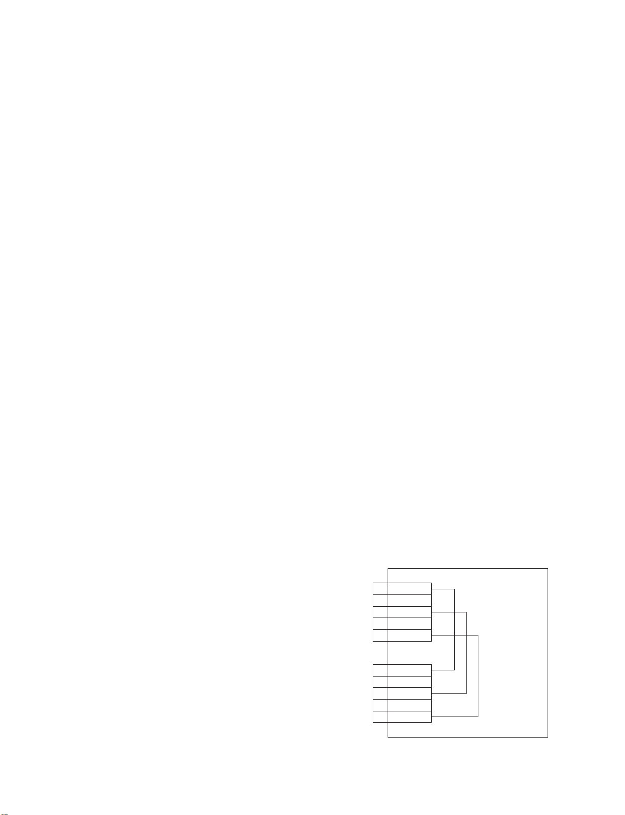
3-3. White Balance Adjustment
3-4. A/D Calibration Adjustment
1. Switch the WINDOW to either TYPE1 or TYPE2.
2. Select the COLOR TEMP “HIGH”.
3. Select RED GAIN and GREEN GAIN. Perform the
white balance adjustment until the color temperature
satisfies the specifications of 9300 K.
Set BLUE GAIN to 255 normally.
4. Select the COLOR TEMP “LOW”.
5. Set BLUE GAIN to 223. Then select RED GAIN and
GREEN GAIN. Perform the white balance adjustment
until the color temperature satisfies the specifications
of 6500 K.
Note : When the white balance at 6500 K cannot be obtained by any means,
decrement the BLUE GAIN by 16 steps and repeat the adjustment of
step 5).
6. Switch the WINDOW to OFF.
Note : When the part number of the B board and that of B1 board has the
suffix of -11, replace the B1 board with the jig board as shown in the
following figure (a).
1. Connect the VGA (640 x 480@60) signal to the
RGB1 input connector.
2. Select the video signal of the 10 % flat field pattern.
3. Set the CAL mode to ON.
4. Check the following values that are shown in the
bottom of the menu in cyan.
R : XXX / G : XXX / B : XXX
Adjust RED BIAS and BLUE BIAS until the following two equations are satisfied.
(G value _1) < R value < (G value +1)
and
(G value _1) < B value < (G value +1)
(Do not adjust GREEN BIAS.)
5. Select the video signal of the maximum brightness 90
% gray scale pattern.
(Select the gray scale pattern that has the left half of
display in black and the right half of display in white.)
6. Check the following values that are shown in the
bottom of the menu in cyan.
R : XXX / G : XXX / B : XXX
Adjust RED BIAS and BLUE BIAS until the following two equations are satisfied.
(G value _1) < R value < (G value +1)
and
(G value _1) < B value < (G value +1)
(Do not adjust GREEN BIAS.)
7. Set the CAL mode to OFF.
PFM-500A3WE/500A3WG/500A3WU/510A2WE/510A2WG/510A2WU
B1 jig board (The B1 jig board is necessary for the B/B1
board that has part number with suffix of -11.)
1
B
2
GND
G
3CN16
GND
4
R
5
B
1
GND
2
G
3CN17
5V–3
4
R
5
Fig. (a)
3-23
Page 76
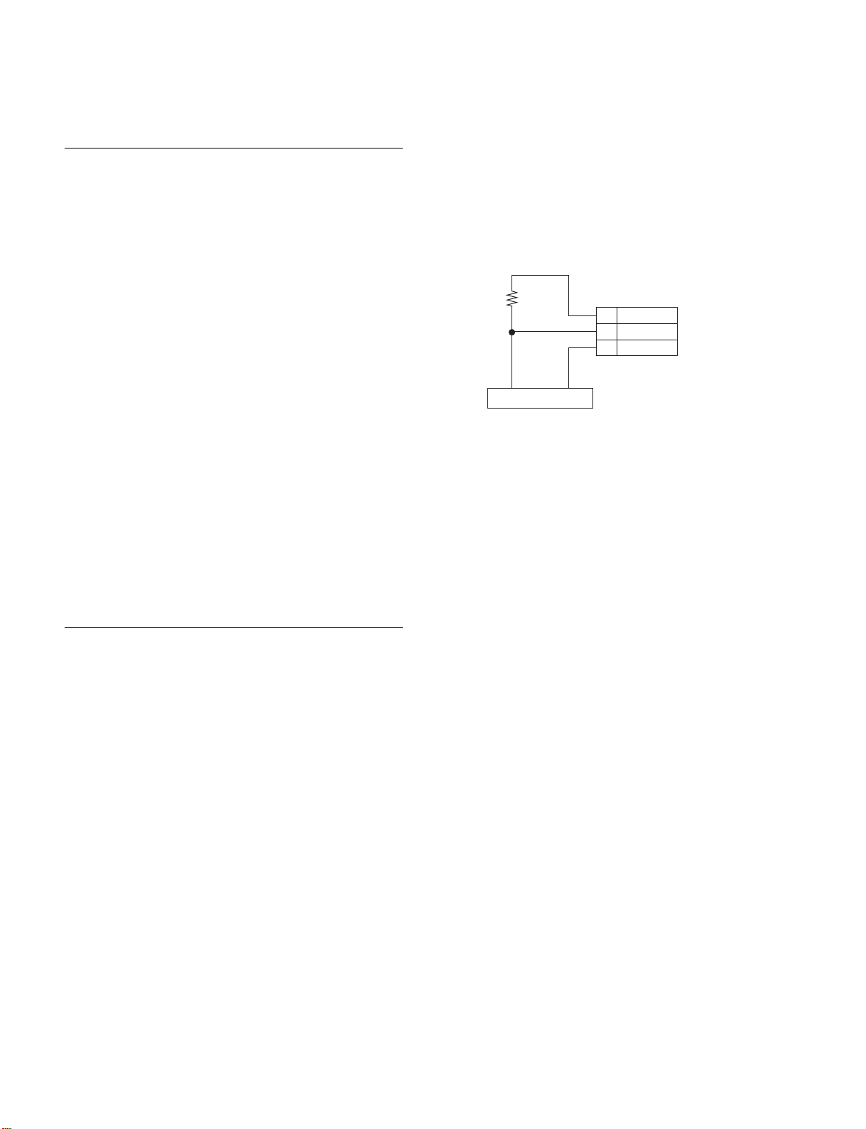
3-5. Video Processor Adjustment
3-6. Watch Error Adjustment
YUV Level Check and Adjustment
1. Connect the 525/60 signal to the YUV input connector.
2. Select the color bar signal.
3. Measure the voltage waveform at pin-14 of IC1003
with an oscilloscope. Confirm that the video signal
excluding sync signal has the following amplitude.
660 mV ± 5 %
(If the video signal excluding sync is outside the
specifications, adjust the video signal level using the Y
GAIN.)
4. Measure the voltage waveform at pin-15 of IC1003
with an oscilloscope. Confirm that the R-Y signal has
the following amplitude.
580 mV ± 5 %
(If the R-Y signal is outside the specifications, adjust
the R-Y signal level using the R-Y GAIN.)
5. Measure the voltage waveform at pin-4 of IC1003 with
an oscilloscope. Confirm that the B-Y signal has the
following amplitude.
700 mV ± 5 %
(If the B-Y signal is outside the specifications, adjust
the B-Y signal level using the B-Y GAIN.)
1. Connect the jig circuit as shown in Fig. (b) and a
frequency counter to the B board CN18.
2. Enter the measurement value on a frequency counter in
the WATCH ERROR.
WATCH ERROR Jig Circuit
1
2
3
Fig. (b)
CN18
VCC
CLOCK
GND
10kΩ
Frequency counter
Cutoff Adjustment
1. Connect the Y signal of the 525/60 signal to the Y
input only of the YUV input connector.
2. Select the gray scale signal.
3. Observe the dark area of display screen. Adjust R
CUTOFF and B CUTOFF until the dark area has
completely no color at all.
3-24
PFM-500A3WE/500A3WG/500A3WU/510A2WE/510A2WG/510A2WU
Page 77
3-7. Switching Regulator
(APS-132 M/136 M Board)
Adjustments
3-7-1. Preparation
1. Remove the switching regulator from the set, and
adjust it under no load.
2. If adjusting the switching regulator with each output
loaded, set as follows.
..
. Load on each output
..
Output Pin No. MIN MAX
VCC CN4 1 pin 1.0 A 5.0 A
VS CN5 2 pin 0.5 A 1.7 A
VA CN5 5 pin 0.5 A 1.5 A
AUDIO +B CN6 3 pin 0.05 A 1.0 A
STBY +5 V CN7 2 pin 0.2 A 0.3 A
5VD CN7 5 pin 1.2 A 1.8 A
6.2 V CN7 8 pin 0.6 A 1.0 A
13.5 V CN7 != pin 0.5 A 1.0 A
13 V CN7 !] pin 0.4 A 1.0 A
3-7-4. VA System Minimum Frequency
Adjustment
1. Short between pin-3 and pin-4 of PH701.
2. Apply 18 V DC to both ends of C169.
3. Connect a frequency counter between gate and source
of Q703.
Note : As the input of frequency counter, use 10 : 1 oscilloscope probes and
raise the input impedance.
4. Adjust the RV700 so that the oscillation frequency is
65 ± 0.5 kHz.
3-7-5. PFC Voltage Adjustment
1. Set the load on each output to the minimum.
2. Apply 100 V AC.
3. Turn the STBY signal ON. (short between CN7 pin-1
and pin-2).
4. Adjust the RV300 so that the voltage across C115 is
385 ± 2 V.
3-7-6. 5 V Adjustment
3-7-2. 13 V System Minimum Frequency
Adjustment
1. Apply 18 V DC to both ends of C169.
2. Connect a frequency counter between gate and source
of Q153.
Note : As the input of frequency counter, use 10 : 1 oscilloscope probes and
raise the input impedance.
3. Adjust the RV150 so that the oscillation frequency is
93 ± 0.5 kHz.
3-7-3. VS System Minimum Frequency
Adjustment
1. Short between pin-3 and pin-4 of PH501.
2. Apply 18 V DC to both ends of C169.
3. Connect a frequency counter between gate and source
of Q503.
Note : As the input of frequency counter, use 10 : 1 oscilloscope probes and
raise the input impedance.
4. Adjust the RV500 so that the oscillation frequency is
49 ± 0.5 kHz.
1. Set the load on each output to the minimum.
2. Apply 100 V AC.
3. Adjust the RV201 so that the voltage of STBY +5 V
output (between CN7 pin-2 and pin-6) is 5.12 ± 0.03 V.
3-7-7. 13.5 V Adjustment
1. Set the load on each output to the minimum.
2. Apply 100 V AC.
3. Turn the STBY signal ON. (short between CN7 pin-1
and pin-2).
4. Adjust the RV250 so that the voltage of 13.5 V output
(between CN7 pin-12 and pin-11) satisfies the following specifications.
Specification value
PFM-500A3W : 13.95 ± 0.05 V
PFM-510A2W : 13.7 ± 0.05 V
PFM-500A3WE/500A3WG/500A3WU/510A2WE/510A2WG/510A2WU
3-25
Page 78

3-7-8. VS Adjustment
3-7-10.VA Adjustment
1. Open the load on VS and VA outputs, and set the load
on the other outputs to the minimum.
2. Apply 100 V AC.
3. Turn the STBY signal ON (short between CN7 pin-1
and pin-2), and also the VRR signal ON (short between CN4 pin-7 and CN7 pin-2).
4. Apply 0 V DC to the VRS (CN4 pin-3).
Use CN4 pin-4 as GND.
5. Adjust the RV402 so that the voltage of VS output
(between CN5 pin-2 and pin-6) is about 149 V.
6. Adjust the RV400 so that the voltage satisfies the
following specifications.
Specification value
PFM-500A3W : 164.3 V
PFM-510A2W : 149.2 V
7. Adjust the RV402 so that the voltage satisfies the
following specifications.
Specification value
PFM-500A3W : 165 ± 0.1 V
PFM-510A2W : 150 ± 0.1 V
1. Open the load on VS and VA outputs, and set the load
on the other outputs to the minimum.
2. Apply 100 V AC.
3. Turn the STBY signal ON (short between CN7 pin-1
and pin-2), and also the VRR signal ON (short between CN4 pin-7 and CN7 pin-2).
4. Apply 0 V DC to the VRA (CN4 pin-5).
Use CN4 pin-6 as GND.
5. Adjust the RV602 so that the voltage of VA output
(between CN5 pin-5 and pin-1) is about 49 V.
6. Adjust the RV600 so that the voltage satisfies the
following specifications.
Specification value
PFM-500A3W : 54.5 V
PFM-510A2W : 49.2 V
7. Adjust the RV602 so that the voltage satisfies the
following specifications.
Specification value
PFM-500A3W : 55 ± 0.1 V
PFM-510A2W : 50 ± 0.1 V
8. Apply 2 V DC to the VRS.
9. Check that the voltage satisfies the following specifications. If the measured value is out of the range,
repeat the above steps from 4, where in step 6, shift the
adjustment value a little, then check the voltage.
Specification value
PFM-500A3W : 185 ± 0.3 V
PFM-510A2W : 170 ± 0.3 V
3-7-9. VS OCP (Only PFM-510A2W)
1. Set the load on each output to the minimum.
2. Apply 100 V AC.
3. Turn the STBY signal ON (short between CN7 pin-1
and pin-2), and also the VRR signal ON (short between CN4 pin-7 and CN7 pin-2).
4. Apply 0 V DC to the VRS (CN4 pin-3).
Use CN4 pin-4 as GND.
5. Connect a voltmeter to the VS output (between CN5
pin-2 and pin-6).
6. Set the load on VS output to 3.8 A, and rotate the
RV401 until the output voltage varies.
Note : Be careful, not to turn excssively, because power can not be
obtained.
8. Apply 2 V DC to the VRA.
9. Check that the voltage satisfies the following specifications. If the measured value is out of the range,
repeat the above steps from 4, where in step 6, shift the
adjustment value a little, then check the voltage.
Note : As the output voltage varies according to the voltage applied to the
VRA, do not shift the applied voltage (2 V DC).
Specification value
PFM-500A3W : 65 ± 0.3 V
PFM-510A2W : 70 ± 0.3 V
3-7-11.VA OCP (Only PFM-510A2W)
1. Set the load on each output to the minimum.
2. Apply 100 V AC.
3. Turn the STBY signal ON (short between CN7 pin-1
and pin-2), and also the VRR signal ON (short between CN4 pin-7 and CN7 pin-2).
4. Apply 0 V DC to the VRA (CN4 pin-5).
Use CN4 pin-6 as GND.
5. Connect a voltmeter to the VA output (between CN5
pin-5 and pin-1).
6. Set the load on VA output to 4.4 A, and rotate the
RV601 until the output voltage varies.
Note : Be careful, not to turn excssively, because power can not be
obtained.
3-26
PFM-500A3WE/500A3WG/500A3WU/510A2WE/510A2WG/510A2WU
Page 79
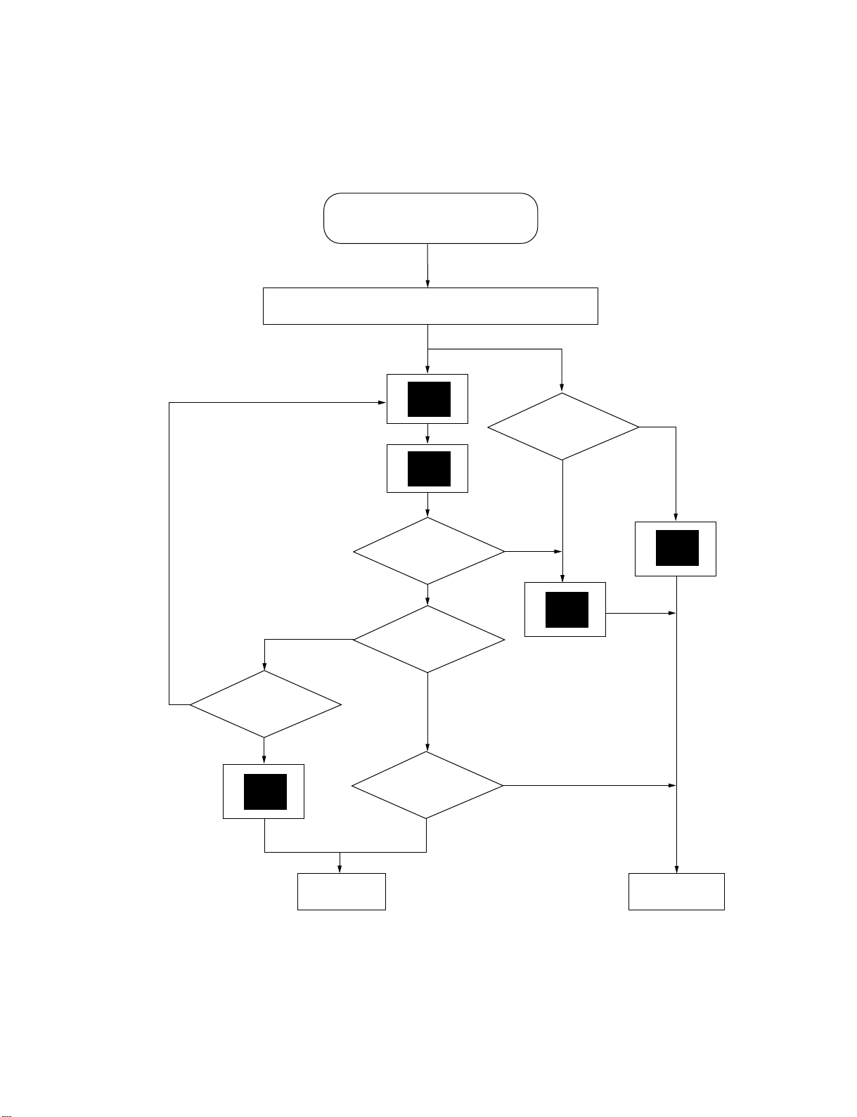
Section 4
Trouble Shooting
4-1. Judging Method When Image Does
Not Appear
1. Flow chart
Image does not appear.
Check service code indicator display.
12
22
Hold down
after about
5 seconds.
N
Y
Power auto
restart?
Y
Hold down
after about
5 seconds.
Y
79
N
.
Power restart
Y
2. How to find PDP unit trouble
1) The power must be supplied normally to the PDP unit.
This power is supplied through two black 8-pin
connectors from the power unit. The kinds of power
supply are 160 V line, 60 V line, and 5 V line.
PFM-500A3WE/500A3WG/500A3WU/510A2WE/510A2WG/510A2WU
3 times or less?
N
99
Check if voltage
is present in DIGITAL
5V line.
PDP failure
N
N
Y
POWER SUPPLY
failure
2) As input signals, H.SYNC (negative polarity), V.SYNC
(negative polarity), BLANKING (negative polarity),
CLOCK and RGB digital data (8 bit x 3) must be
entered normally and DISPEN must be “high”.
If no images appears through the above conditions are
satisfied, the PDP unit will be defective.
4-1
Page 80

4-2. Self Diagnosis Function
4-2-2. Criteria for Judgment of Abnormality
4-2-1. Outline
The PFM-500A3W/510A2W has the self diagnosis
function using A/D converter to detect the power supply
analog voltages, 8 channels of temperature sensor, fan
operations, power unit temperature, DC voltage status, and
to check the EEPROM and the watch register. When any
abnormality occurs or defect is detected, the Error Code
appears on the service code indicator of the power supply
block, the standby indicator on the control panel flashes
and the detected data is displayed on the service menu
[STATUS/TEST] block. If the abnormal status exceeds
the allowable limit, the PFM-500A3W/510A2W is forced
to shut down.
The detection items are shown as follows.
1. Increase and decrease of the panel DC voltage Vs is
detected.
2. Increase and decrease of the panel DC voltage Va is
detected.
3. Increase of temperature at the side of the power block
in the top of the panel is detected and shut down of the
machine.
4. Increase of temperature at the center in the top of the
panel is detected and shut down of the machine.
5. Increase of temperature at the side of the input connector block in the top of the panel is detected and shut
down of the machine.
6. Detection of outside environment temperature.
7. Detection of fan stop and that of drive circuit failure.
* Three fans at the top of the panel and two fans for
power supply.
8. Detection of temperature rise in the power supply
block.
9. Shut down when the 5 V for internal digital circuit has
abnormality.
10. Detection of failure of the EEPROM.
11. Detection of abnormality in communication with scan
converter.
12. Detection of failure in the ON/OFF control of power
supply.
13. Detection of decreased backup power supply voltage
for watch and detection of abnormality in oscillator.
14. Detection of PDP failure using the combination of the
voltage detection and shut down of the machine.
4-2
1.
Increase and decrease of the panel DC voltage Vs is detected.
(Name of this function on the service menu :
POWER SUPPLY - PDP VS)
..
. PFM-510A2W
..
The normal operating range is + 160 V + 24 V/_ 22 V.
Warning of increase of the voltage Vs when 184 V or
more : Service code [11]
Warning of decrease of the voltage Vs when 138 V or
less : Service code [12]
..
. PFM-500A3W
..
The normal operating range is + 175 V + 26 V/_ 23 V.
Warning of increase of the voltage Vs when 201 V or
more : Service code [11]
Warning of decrease of the voltage Vs when 152 V or
less : Service code [12]
2.
Increase and decrease of the panel DC voltage Va is detected.
(Name of this function on the service menu :
POWER SUPPLY - PDP VA)
The normal operating range is + 60 V + 15 V/_ 14 V.
Warning of increase of the voltage Va when 75 V or
more : Service code [21]
Warning of decrease of the voltage Va when 46 V or
less : Service code [22]
3.
Increase of temperature at the side of the power block in the
top of the panel is detected and shut down of the machine.
(Name of this function on the service menu :
TEMPERATURE - P/S BLOCK SIDE)
The normal operating range is up to 57 °C.
Warning of high temperature when 58 °C or higher :
Service code [31]
Shut down at the temperature of 68 °C or higher :
Service code [39]
4. Increase of temperature at the center in the top of the
panel is detected and shut down of the machine.
(Name of this function on the service menu :
TEMPERATURE - CENTER)
The normal operating range is up to 55 °C.
Warning of high temperature when 56 °C or higher :
Service code [A1]
Shut down at the temperature of 66 °C or higher :
Service code [A9]
5. Increase of temperature at the side of the input connector block in the top of the panel is detected and shut
down of the machine.
(Name of this function on the service menu :
TEMPERATURE - I/O BLOCK SIDE)
The normal operating range is up to 53 °C.
Warning of high temperature when 54 °C or higher :
Service code [41]
Shut down at the temperature of 64 °C or higher :
Service code [49]
PFM-500A3WE/500A3WG/500A3WU/510A2WE/510A2WG/510A2WU
Page 81

6. Detection of outside environment temperature
(Name of this function on the service menu :
TEMPERATURE - AMBIENT TEMP)
Occurrence of abnormality and fault is judged solely
from the internal temperature of the PFM-500A3W/
510A2W. Measurement of the ambient temperature
aims mainly at the confirmation of the operating
environment. Therefore, there is no chance to indicate
this warning message.
Warning of high temperature at 60 °C or higher :
Service code [F1]
7. Detection of fan stop and that of drive circuit failure.
. Detection if fan is stopped or not.
(Name of this function on the service menu : FAN - I/O
BLOCK SIDE, CENTER, P/S BLOCK SIDE, No. 1, No. 2)
Status of the respective fans are displayed as OK or
NG on the service menu STATUS.
. Fan of the power supply block at the top of the rear
of the machine : Service code [55]
. Fan in the center of the top on the rear of the ma-
chine : Service code [54]
. Fan on the input terminal at the top on the rear of the
machine : Service code [53]
. Two fans of the power supply block :
Service code [52]
or [51]
. Detection of fan drive circuit failure
(Name of this function on the service menu :
FAN - DRIVE CIRCUIT)
The warning when the fan drive data is 6 V or more
and the actual drive voltage is 2 V or less :
Service code [58]
8. Detection of temperature rise in the power supply block.
(Name of this function on the service menu :
TEMPERATURE - P/S INTERNAL)
Warning of high temperature when temperature of the
heat sink for main converter inside the power supply
unit exceeds the allowable limit : Service code [61]
9. Shut down when the 5 V for internal digital circuit has
abnormality.
(Name of this function on the service menu :
POWER SUPPLY - DIGITAL 5V)
The voltage that is input to pin-62 of the system
controller (IC252) is detected.
Shut down when there is no input voltage :
Service code [79]
10. Detection of failure of the EEPROM.
(Name of this function on the service menu : Nil)
Warning when communication with EEPROM cannot
be performed normally.
EEPROM ID code error : Service code [81]
EEPROM data write error : Service code [82]
EEPROM data read error : Service code [83]
EEPROM failure : Service code [85]
11. Detection of abnormality in communication with scan
converter.
(Name of this function on the service menu : Nil)
Warning when communication with scan converter
cannot be performed normally.
EEPROM ID code error : Service code [91]
12. Detection of failure in the ON/OFF control of power
supply.
(Name of this function on the service menu : Nil)
When the digital 5 V power does not decrease even in
the STBY state, the machine enters the POWR ON
state automatically : Service code [98]
13. Detection of decreased voltage of the backup power
supply for watch and detection of abnormality of
oscillator.
(Name of this function on the service menu : Nil)
Normal/abnormal is detected from the register value
inside the watch IC.
Initialization of time due to abnormal register value :
Service code [B1]
Warning of low voltage of backup power supply :
Service code [B2]
Warning that crystal oscillator for watch has stopped :
Service code [B3]
14. Detection of PDP failure using the combination of the
voltage detection and shut down of the machine.
(Name of this function on the service menu : Nil)
PDP is suspected to be defective when DIGITAL 5 V
is normal among the voltages (VS, VA, DIGITAL 5
V) required to drive PDP while both VS and VA are
not inputted.
When all the following conditions are satisfied, the
machine enters once to the STANDBY mode then turn
the main power back on again.
1) DC 180 V power is 40 V or less.
2) DC 70 V power is 20 V or less.
3) DIGITAL 5 V is normal.
The above-described operation is repeated three times.
If the above three conditions are still satisfied, the PDP
is judged to be faulty and the main power is shut
down.
Service code [99]
PFM-500A3WE/500A3WG/500A3WU/510A2WE/510A2WG/510A2WU
4-3
Page 82
4-3. Error Code Table
Error Code
on Display
11 Warning of increase of panel high voltage (Vs) POWER SUPPLY PDP VS
12 Warning of decrease of panel high voltage (Vs) POWER SUPPLY PDP VS
21 Warning of increase of panel middle voltage (Va) POWER SUPPLY PDP VA
22 Warning of decrease of panel middle voltage (Va) POWER SUPPLY PDPVA
31 Warning of increase of temperature at the TEMPERATURE P/S BLOCK SIDE
power supply block in the top of the panel
39 Power shut down due to increase of temperature TEMPERATURE P/S BLOCK SIDE
at the power supply block in the top of the panel
A1 Warning of increase of temperature at the center of the top of the panel TEMPERATURE CENTER
A9 Power shut down due to increase of temperature TEMPERATURE CENTER
at the center of the top of the panel
41 Warning of increase of temperature at the TEMPERATURE I/O BLOCK SIDE
input/output block of the top of the panel
49 Power shut down due to increase of temperature TEMPERATURE I/O BLOCK SIDE
at the input/output block of the top of the panel
51 Warning of stoppage of air intake fan-1 of the power supply block FAN No.1
52 Warning of stoppage of air intake fan-2 of the power supply block FAN No.2
53 Warning of stoppage of fan at the input/output block of the panel top FAN I/O BLOCK SIDE
54 Warning of stoppage of fan at the center of the panel top FAN CENTER
55 Warning of stoppage of fan of the power supply block FAN P/S BLOCK SIDE
in the top of the panel
58 Failure of fan drive circuit FAN DRIVE CIRCUIT
79 Power shut down due to decrease of DIGITAL 5 V
81 EEPROM ID error
82 EEPROM write error
83 EEPROM read error
85 EEPROM is defective
91 Communication with scan converter is defective
98 Failure that voltage does not decrease at POWER OFF
99 Panel is defective
B1 Warning of initialization of time data due to watch control error
B2 Decrease of the backup power voltage for watch
B3 Oscillator for watch is defective
F1 Warning of increase of ambient temperature
Abnormal/Defective State Name of Function
4-4
PFM-500A3WE/500A3WG/500A3WU/510A2WE/510A2WG/510A2WU
Page 83
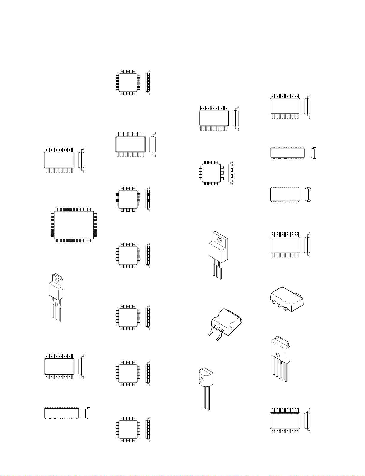
Section 5
Semiconductors
IC
24LC21T/SN
BA10358F-T2
CXA1211M-T4
LM1881MX
M24C04-WMN6T
M24C64-WMN6T
MM1113XFBE
NJM2903M-T2
NJM2904E(TE2)
ST49C101ACF8-05-TR
TC4W53FU(TE12R)
TC4W66F(TE12R)
TC7W126FU(TE12R)
TL026CPS-E05
µPC358G2-T1
1
TOP VIEW
8pin SOP
AD9884AKS-140
102
103
128
138
TOP VIEW
65
64
39
CXA1860Q-T4
CXD2300Q-T4
1
TOP VIEW
32pin QFP
CXA2119M-T6
MB90096PF-G-182-BND-ER
1
TOP VIEW
28pin SOP
CXD2030R
1
TOP VIEW
144pin QFP
CXD2090Q
ICS9161A-01CW16T
MAX202CSE-T
MC74HC4052F-T2
MC74HC4538AF-T1
MC74HC595AF-T2
TC74HC123AF(EL)
TC74HC157AF(EL)
TC74HC4053AF(EL)
1
TOP VIEW
16pin SOP
ISPLSI2192VE-100LT128
1
TOP VIEW
128pin QFP
LM2940CT-12FL91
LM2940CT-5.0
LM2940CT-9.0
M52347FP-TE
M62352GP-75ED
TC74HCT244AF(EL)
TC74LCX244F(EL)
TC74VHCT245AFT(EL)
TDA8395T/N3
1
TOP VIEW
20pin SOP
MC68HC05P6SC442119B
1
TOP VIEW
28pin DIP
MSM514265C-60JSDR1
1
TOP VIEW
40pin SOJ
MSM56V16160D-10TS-K
BA033FP-E2
1
TOP VIEW
208pin QFP
CXD2309Q-T6
ISPLSI2032E-110LT48
VCC
GND
OUT
1
TOP VIEW
BA7657F-E2
48pin QFP
TA8184F(EL)
EPFQC240AA
1
TOP VIEW
24pin SOP
CXA1739S
1
TOP VIEW
240pin QFP
HD64F2633TE
1
TOP VIEW
48pin DIP
1
TOP VIEW
PFM-500A3WE/500A3WG/500A3WU/510A2WE/510A2WG/510A2WU
120pin QFP
INPUT
GND
OUTPUT
LM317T
ADJ
INPUT
LM35DZ
3
2
1
OUTPUT
1
TOP VIEW
50pin SOP
PQ07VZ012P
1
2
3
PQ3TZ53U
1
5
RS5C348A-E2
1
TOP VIEW
10pin SOP
5-1
Page 84
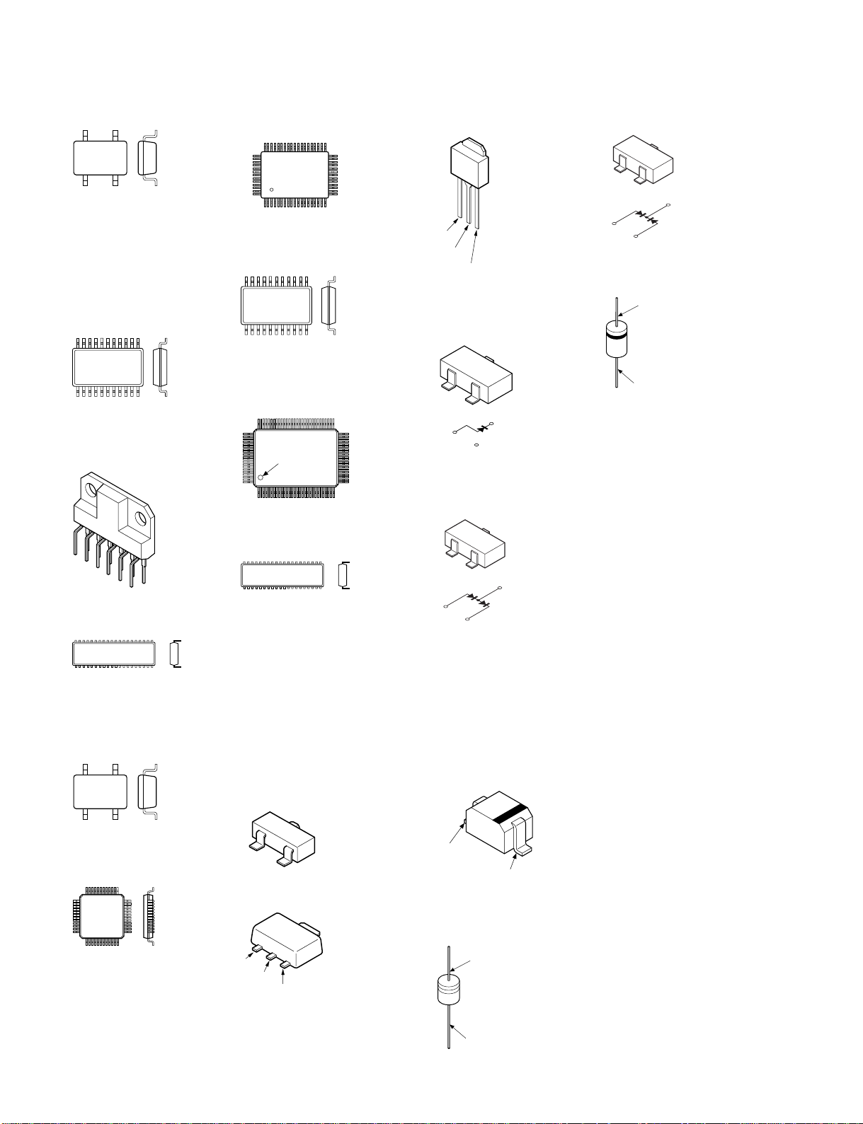
IC, Transistor, Diode
S-80842ANNP-ED6-T2
1
4pin CHIP
SN74LVC125APWR
TC74HC04AF-TP2
TC74HC125AF(EL)
TC74VHC14F(EL)
TC74VHCT04AF(EL)
TLC2932IPW-E20
TLC2933IPWR
1
TOP VIEW
14pin SOP
TA8216H
1
12
TC74HC126AF(EL)
1
TOP VIEW
14pin DIP
TC7S04F(TE85R)
TC7S04FU(TE85R)
TC7S08FU(TE85R)
1
5pin CHIP
THC63LVDF84A-T
1
TOP VIEW
56pin QFP
TLC5733AIPM
3351
52
64
TOP VIEW
32
20
191
UPC1862GS-E2
1
TOP VIEW
36pin SOP
UPD64082GF-3BA
5180
81
100
INDEX
1
TOP VIEW
50
31
30
Z8622812PSC
1
TOP VIEW
18pin DIP
2SA1036K-T-146-R
2SA1037AK-T146-QR
2SA1037K-T-146-S
2SB709A-QRS-TX
2SC2412K-T-146-Q
2SC2412K-T-146-QR
2SC2412K-T-146-R
2SC2412K-T-146-S
DTA114EKA-T146
DTA144EKA-T146
DTC114EKA-T146
DTC144EKA-T146
C
B
E
2SA1213Y-TE12L
B
C
E
2SJ377(TE16L)
G
D
S
02CZ10-TE85L
RD5.6M-T1B2
3
2
1
3
2
1
1SS226-TE85L
MA157-TX
3
2
1
3
2
1
1SS355TE-17
DTZ-TT11-3.3B
HVU359TRF
MA111-TX
UDZ-TE-17-12B
UDZ-TE-17-3.9B
UDZ-TE-17-36B
UDZ-TE-17-4.7B
UDZ-TE-17-5.6B
ANODE
CATHODE
D1N20R-TR
RD10ES-T1B2
CATHODE
DAN202K-T-146
3
2
1
3
2
1
RD33ES-T1B2
CATHODE
ANODE
5-2
ANODE
PFM-500A3WE/500A3WG/500A3WU/510A2WE/510A2WG/510A2WU
Page 85

NOTE :
The components identified marked ! are
critical for safety.
Replace only with the part number specified.
Les composants identifiés par la marque !
sont critiques pour la sécurité.
Ne les remplacer que par une pièce portant
le numéro spécifié.
Section 6
Exploded Views
• Items marked “ * ” are not stocked since they are seldom required
for routine service. Some delay should be anticipated when ordering these items.
• Items with no part number and no description are not stocked because they are seldom required for routine service.
• The construction parts of an assembled part are indicated with a
collation number in the remarks column.
PFM-500A3WE/500A3WG/500A3WU/510A2WE/510A2WG/510A2WU
6-1
Page 86
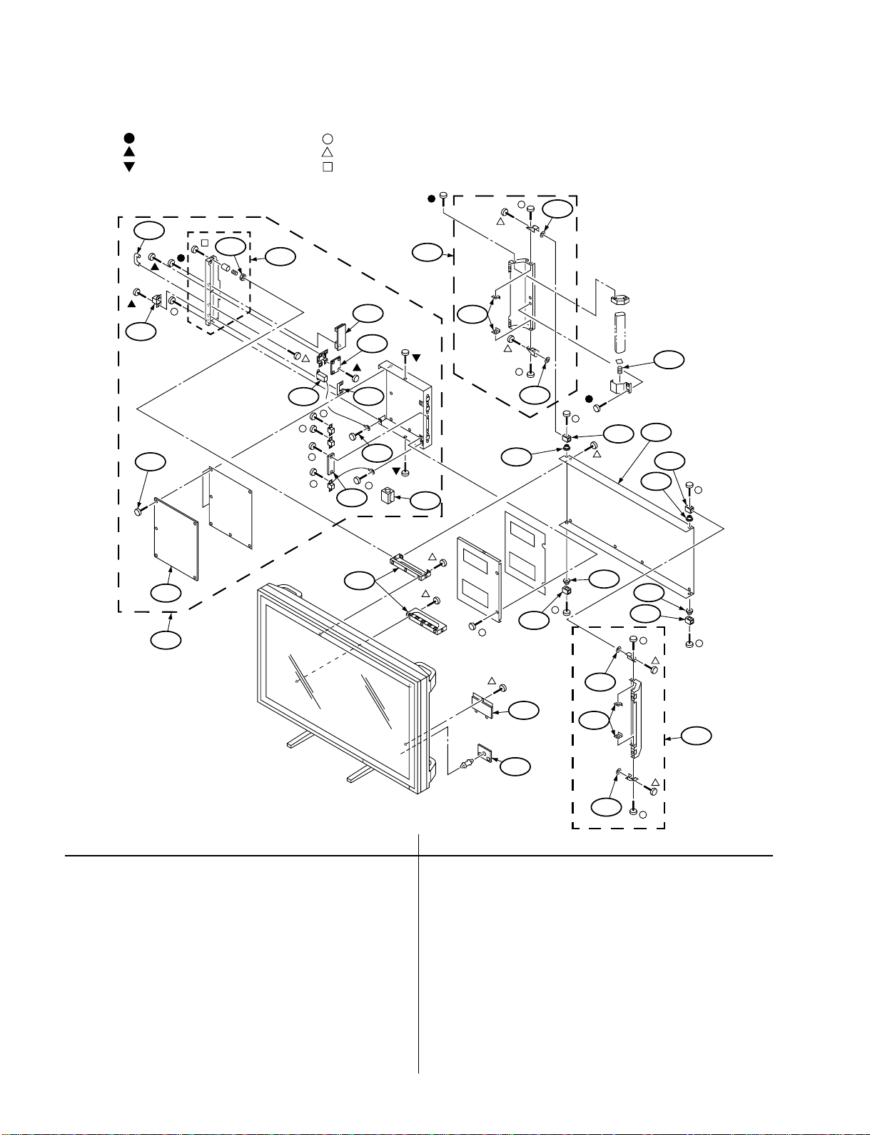
Power Block
6-1. Power Block
: 7-685-648-79 +BVTP3x12
: 7-682-950-09 +PSW3x12
: 7-682-249-04 +K3x10
1
4
3
: 7-682-949-09 +PSW3x10
: 7-682-962-09 +PSW4x10
: 7-682-566-04 +B4x20
14
13
5
2
8
9
11
23
6
7
9
10
22
12
15
16
14
19
18
17
17
18
14
20
15
18
17
17
18
13
1 4-052-200-01 HANDLE, PROTECTOR
2 2-990-241-02 HOLDER (A), PLUG
3 * X-4036-671-3 PANEL ASSY, POWER UNIT 4
4 * 3-648-057-00 NUT (ISO-4), U
5 * A-1373-813-A UA MOUNT
6 * A-1272-048-A AF MOUNT
7 3-625-620-00 BRACKET , AC CONNECTOR
8 ! 1-540-178-21 INLET, AC (GL-2100C-30)
9 4-066-309-01 SCREW, MACHINE, (+) P M4X8
10 * A-1311-857-A G2 MOUNT (PFM-500A3W)
10 * A-1311-853-A G2 MOUNT (PFM-510A2W)
11 1-468-522-11 REGULATOR, SWITCHING
(APS-136 M BOARD) (PFM-500A3W)
11 1-468-447-11 REGULATOR, SWITCHING
(APS-132 M BOARD) (PFM-510A2W)
6-2
21
14
Ref.No. Part No. Description RemarkRef.No. Part No. Description Remark
12 1-543-653-11 CORE ASSY , BEAD(DIVISION TYPE)
(PFM-510A2W)
13 * X-4035-827-1 COVER ASSY , SIDE 14, 15
14 3-696-510-01 WASHER (3), STOPPER
15 4-065-249-01 NUT, PLATE
16 3-669-594-00 SPRING, COMPRESSION
17 * 4-075-284-01 SPACER
18 4-065-239-01 NUT
19 * 4-074-162-01 COVER, REAR
20 * 4-065-262-01 COVER, HAND HOLE
21 * A-1372-828-A H6 MOUNT
22 * X-4035-835-2 BRACKET ASSY (A), REAR COVER
23 * A-1484-854-A
23
* A-1484-837-A
PFM-500A3WE/500A3WG/500A3WU/510A2WE/510A2WG/510A2WU
POWER BLOCK ASSY (PFM-500A3W) 1-17
POWER BLOCK ASSY (PFM-510A2W) 1-17
Page 87
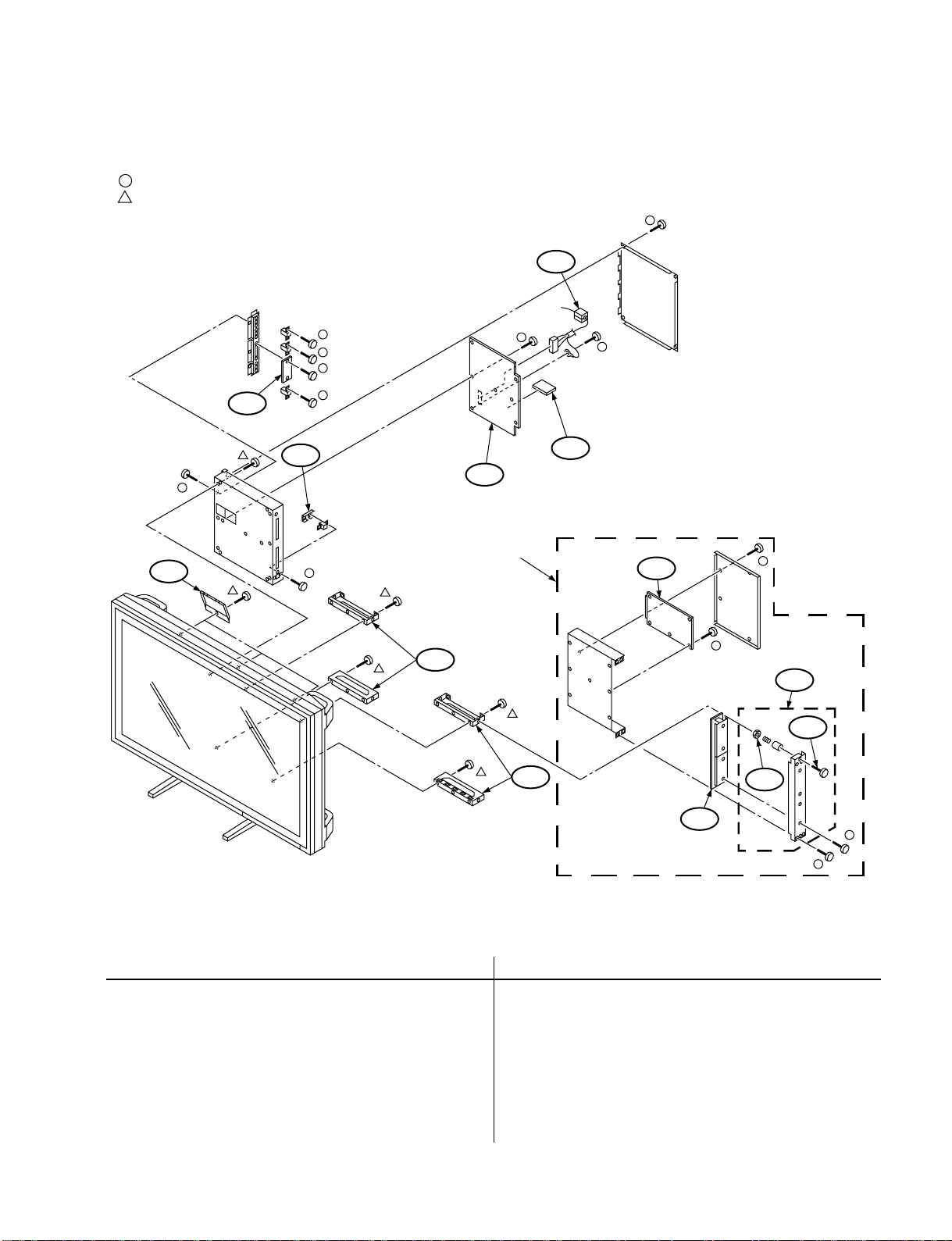
6-2. SC and I/O Blocks
: 7-682-949-09 +PSW3x10
: 7-682-962-09 +PSW4x10
51
SC and I/O Blocks
55
56
52
57
53
BKM-500
58
54
63
59
60
61
62
51 * A-1311-858-A G1 MOUNT (PFM-500A3W)
51 * A-1311-854-A G1 MOUNT (PFM-510A2W)
52 4-065-253-01 NUT (A), PLATE
53 * A-1131-604-A B MOUNT (PFM-500A3W)
53 * A-1131-595-A B MOUNT (PFM-510A2W)
54 * A-1131-596-A B1 MOUNT
55 1-500-037-11 CORE, FERRITE (WITH CASE)
56 * 4-067-117-01 COVER, FAN
57 * X-4035-917-2 BRACKET ASSY (B), REAR COVER
58 * X-4035-835-2 BRACKET ASSY (A), REAR COVER
PFM-500A3WE/500A3WG/500A3WU/510A2WE/510A2WG/510A2WU
Ref.No. Part No. Description RemarkRef.No. Part No. Description Remark
59 * X-4035-837-3 PANEL ASSY, I/O UNIT 60, 61
60 * 4-050-804-01 SCREW, PANEL STOPPER
61 * 3-648-057-00 NUT (ISO-4), U
62 * A-1373-812-A UJ MOUNT
63 * A-1372-829-A H1 MOUNT
6-3
Page 88
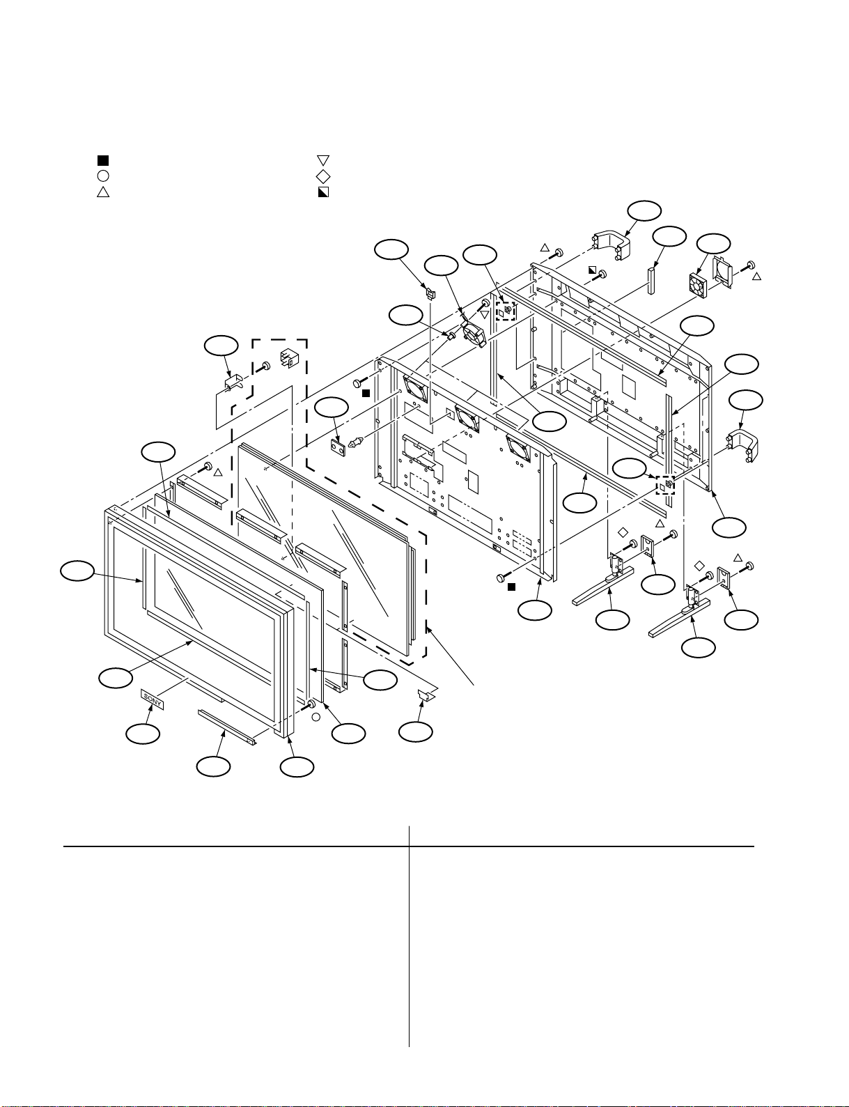
Cabinet Block
6-3. Cabinet Block
: 7-682-973-49 +PSW5x16
: 7-682-949-09 +PSW3x10
: 7-682-962-09 +PSW4x10
118
115
: 7-682-970-09 +PSW4x40
: 7-682-965-01 MACHINE SCREW +P M4x16
: 7-628-000-08 +PSW5x50
123
104
103
105
106
120
119
106
108
122
109
119
120
108
107
116
115
113
101
101 1-475-914-12 BOARD UNIT , KEY
102 1-758-502-11 GLASS, OPTICAL FILTER
(PFM-500A3W)
102 * 1-758-411-11 GLASS, OPTICAL FILTER
(PFM-510A2W)
103 * A-1391-046-A S1 MOUNT
104 4-062-616-01 BUSHING, RUBBER
105 1-763-144-11 FAN, DC
106 X-4035-885-1 NUT ASSY , PLATE
107 * X-4037-115-1 CABINET ASSY, REAR
108 * 4-070-197-01 HANDLE
109 1-763-370-11 FAN, DC (WITH SENSOR)
114
102
116
121
PANEL,PLASMA DISPLAY
FPF42C128128UA-01 (PFM-510A2W)
117
FPF42C10660UE-21 (PFM-500A3W)
(Made by Fujitsu)
Ref.No. Part No. Description RemarkRef.No. Part No. Description Remark
110 * 4-065-296-01 COVER, FOOT
111 * X-4035-829-1 FOOT (L) ASSY
112 * X-4035-828-1 FOOT (R) ASSY
113 * X-4036-360-1 EMBLEM ASSY
114 X-4035-913-2 BEZEL ASSY
115 * 4-065-188-31 GASKET
116 * 4-065-188-21 GASKET
117 * 4-070-356-01 PLATE, PROTECTION
118 * 4-070-357-01 PLATE, EARTH
119 * 4-071-740-01 GASKET
120 * 4-071-739-01 GASKET
121 * X-4035-832-7 SHIELD ASSY, MAIN
122 * 4-071-738-01 GASKET
123 * 3-646-071-02 HOLDER, WIRE
111
110
110
112
6-4
PFM-500A3WE/500A3WG/500A3WU/510A2WE/510A2WG/510A2WU
Page 89
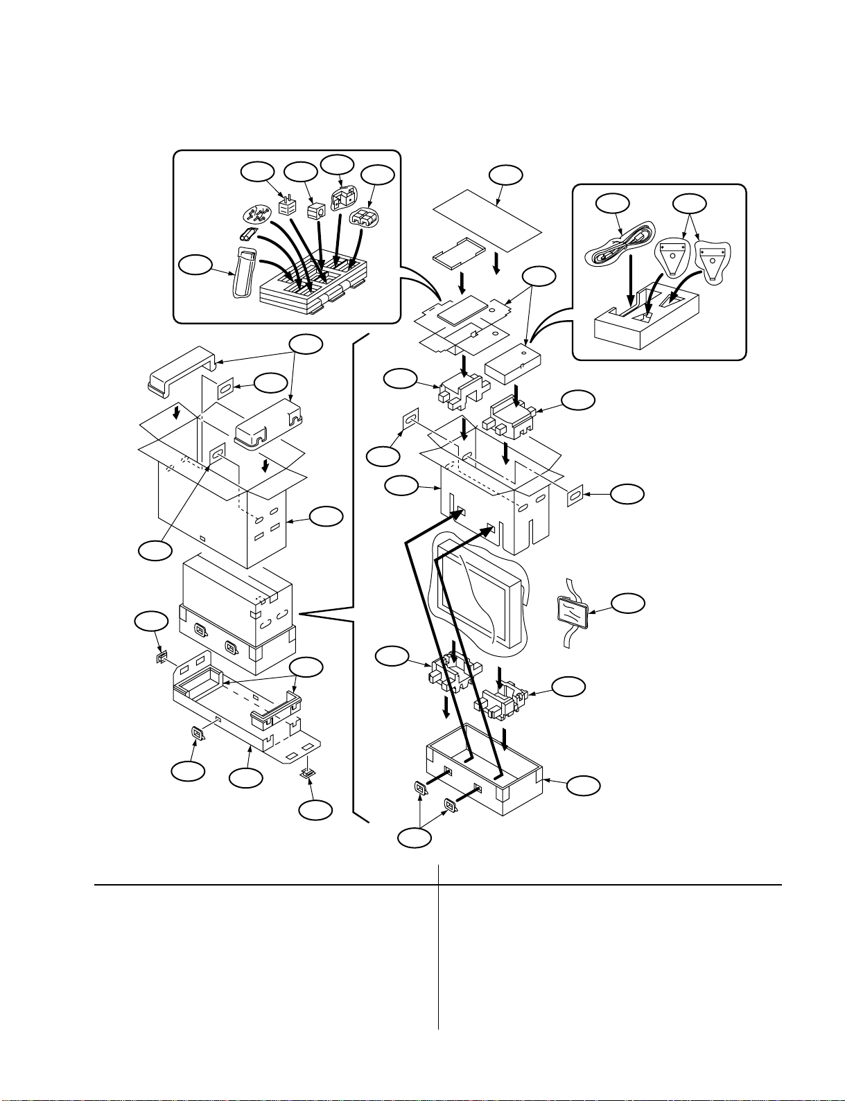
6-4. Packing Materials
Packing Materials
155
170
169
155
168
160
161
167
166
155
153
154
151
152
153
165
164
155
163
157
159
159
160
162
163
151 * 4-066-055-01 BOARD, TOP
152 * 4-069-139-01 BOX, ACCESSORY
153 * 4-069-133-01 CUSHION (UPPER) (ASSY)
154 * 4-070-492-02 INDIVIDUAL CARTON 155
155 * 3-704-066-01 HANDLE (B)
156 4-076-854-01 OPERATING INSTRUCTIONS
157 * 4-069-134-01 CUSHION (LOWER) (ASSY)
158 * 4-065-581-01 TRAY
159 * 3-674-673-01 STOPPER (A)
160 * 4-070-419-01 CUSHION (A)
156
157
158
Ref.No. Part No. Description RemarkRef.No. Part No. Description Remark
161 * 4-070-417-02 INDIVIDUAL CARTON (A) 155
162 * 4-070-418-01 TRAY (A)
163 * 4-396-077-01 JOINT
164 * 4-072-155-01 REINFORCEMENT, FOOT
165 ! 1-558-527-11 CORD SET , POWER (13A/125V) (U/C)
(
! 1-590-151-11 CORD SET, POWER (10A/250V) (AEP, E)
166 1-543-653-1 1 CORE ASSY , BEAD(DIVISION TYPE)
167 * 4-065-463-01 BRACKET, FOOT
168 2-990-242-01 HOLDER (B), PLUG
169 1-750-686-11 CONNECTOR, CONVERSION (3P-2P)
170 1-475-089-11 REMOTE COMMANDER (RM-921)
PFM-500A3WE/500A3WG/500A3WU/510A2WE/510A2WG/510A2WU
6-5
Page 90
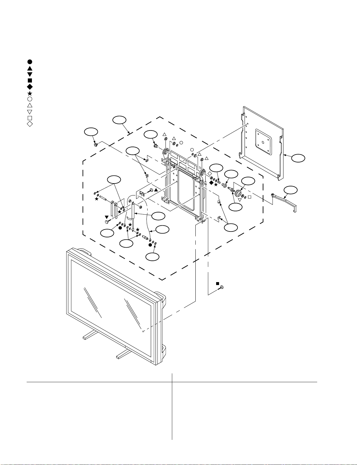
MB-514
6-5. MB-514
: 7-688-005-02 W5
: 7-682-948-09 +PSW3x8
: 7-682-961-09 +PSW4x8
: 7-682-973-49 +PSW5x16
: 7-623-213-22 SW6
: 7-688-006-12 W6
: 7-624-197-71 C20
: 7-688-000-26 W20
: 7-688-000-25 W16
: 7-624-197-31 C16
: 7-684-026-04 N6
14
1
2
3
13
8
4
9
11
12
10
6
5
4
7
5
3
1 * X-4035-976-1 BRACKET ASSY , MOUNTING 2-11
2 * 4-066-350-01 SHAFT (B), FIXED
3 * 4-066-365-01 GUARD, EDGE
4 3-618-078-00 RING, RETAINING, CE TYPE
5 3-638-493-02 RING, RETAINING, CE
6 * 4-066-363-01 DAMPER, GAS
7 4-066-364-01 ROPE, WIRE
8 * 4-066-351-01 SPRING, COMPRESSION
9 * 4-066-349-02 SHAFT (A), FIXED
10 * 4-066-362-01 PIN
6-6
Ref.No. Part No. Description RemarkRef.No. Part No. Description Remark
11 * 4-066-361-01 BRACKET , LOCK
12 X-4035-975-1 HANDLE ASSY
13 * X-4035-977-2 BRACKET ASSY , WALL
14 4-066-358-02 KNOB
PFM-500A3WE/500A3WG/500A3WU/510A2WE/510A2WG/510A2WU
Page 91
NOTE :
The components identified marked ! are
critical for safety.
Replace only with the part number specified.
Les composants identifiés par la marque !
sont critiques pour la sécurité.
Ne les remplacer que par une pièce portant
le numéro spécifié.
* A-1272-048-A AF MOUNT
***********
Section 7
AF B
Electrical Parts List
• Items marked “ * ” are not stocked since they are seldom required
for routine service. Some delay should be anticipated when
ordering these items.
• Due to standardization, replacements in the parts list may be
different from the parts specified in the diagrams or the components
used on the set.
RESISTORS
• All resistors are in ohms.
• F: nonflammable
• METAL: Metal-film resistor
• METAL OXIDE: Metal oxide-film resistor
Ref.No. Part No. Description RemarkRef.No. Part No. Description Remark
* A-1136-120-A B COMPL (PFM-500A3W)
* A-1136-118-A B COMPL (PFM-510A2W)
**********
<CAPACITOR>
C6501 1-126-392-11 ELECT CHIP 100µF 20% 6.3V
C6502 1-164-004-11 CERAMIC CHIP 0.1µF 10% 25V
C6503 1-164-004-11 CERAMIC CHIP 0.1µF 10% 25V
<CONNECTOR>
CN6501 * 1-564-520-11 PLUG, CONNECTOR 5P
<IC>
IC6501 8-759-032-59 IC MC74HC595AF-T2
IC6502 8-759-032-59 IC MC74HC595AF-T2
IC6503 8-719-045-58 DIODE LB-602MA2
<RESISTOR>
R6501 1-216-041-00 RES-CHIP 470 5% 1/10W
R6502 1-216-041-00 RES-CHIP 470 5% 1/10W
R6503 1-216-041-00 RES-CHIP 470 5% 1/10W
R6504 1-216-041-00 RES-CHIP 470 5% 1/10W
R6505 1-216-041-00 RES-CHIP 470 5% 1/10W
R6506 1-216-041-00 RES-CHIP 470 5% 1/10W
R6507 1-216-041-00 RES-CHIP 470 5% 1/10W
R6508 1-216-041-00 RES-CHIP 470 5% 1/10W
R6509 1-216-041-00 RES-CHIP 470 5% 1/10W
R6510 1-216-041-00 RES-CHIP 470 5% 1/10W
R6511 1-216-041-00 RES-CHIP 470 5% 1/10W
R6512 1-216-041-00 RES-CHIP 470 5% 1/10W
R6513 1-216-041-00 RES-CHIP 470 5% 1/10W
R6514 1-216-041-00 RES-CHIP 470 5% 1/10W
R6515 1-216-041-00 RES-CHIP 470 5% 1/10W
R6516 1-216-041-00 RES-CHIP 470 5% 1/10W
* 1-526-652-21 SOCKET, IC (DP) 8P
4-382-854-01 SCREW (M3X8), P, SW (+)
<HOLDER, BATTERY>
BAT500 1-550-104-11 HOLDER, BATTERY
<CAPACITOR>
C1 1-126-934-11 ELECT 220µF 20% 16V
C2 1-126-934-11 ELECT 220µF 20% 16V
C3 1-126-934-11 ELECT 220µF 20% 16V
C4 1-126-934-11 ELECT 220µF 20% 16V
C6 1-164-004-11 CERAMIC CHIP 0.1µF 10% 25V
C7 1-164-004-11 CERAMIC CHIP 0.1µF 10% 25V
C8 1-164-004-11 CERAMIC CHIP 0.1µF 10% 25V
C9 1-164-004-11 CERAMIC CHIP 0.1µF 10% 25V
C10 1-164-004-11 CERAMIC CHIP 0.1µF 10% 25V
C12 1-126-934-11 ELECT 220µF 20% 16V
C13 1-104-664-11 ELECT 47µF 20% 16V
C14 1-164-004-11 CERAMIC CHIP 0.1µF 10% 25V
C15 1-164-004-11 CERAMIC CHIP 0.1µF 10% 25V
C16 1-164-004-11 CERAMIC CHIP 0.1µF 10% 25V
C18 1-164-004-11 CERAMIC CHIP 0.1µF 10% 25V
C19 1-126-934-11 ELECT 220µF 20% 16V
C20 1-126-934-11 ELECT 220µF 20% 16V
C21 1-126-934-11 ELECT 220µF 20% 16V
C23 1-126-934-11 ELECT 220µF 20% 16V
C24 1-164-004-11 CERAMIC CHIP 0.1µF 10% 25V
C25 1-126-934-11 ELECT 220µF 20% 16V
C26 1-164-004-11 CERAMIC CHIP 0.1µF 10% 25V
C27 1-126-934-11 ELECT 220µF 20% 16V
C100 1-164-004-11 CERAMIC CHIP 0.1µF 10% 25V
C101 1-164-004-11 CERAMIC CHIP 0.1µF 10% 25V
***************************************************************
PFM-500A3WE/500A3WG/500A3WU/510A2WE/510A2WG/510A2WU
C102 1-163-021-91 CERAMIC CHIP 0.01µF 10% 50V
C103 1-163-021-91 CERAMIC CHIP 0.01µF 10% 50V
C104 1-115-566-11 CERAMIC CHIP 4.7µF 10% 10V
C105 1-115-566-11 CERAMIC CHIP 4.7µF 10% 10V
C106 1-115-566-11 CERAMIC CHIP 4.7µF 10% 10V
7-1
Page 92

B
C107 1-115-566-11 CERAMIC CHIP 4.7µF 10% 10V
C108 1-107-713-11 ELECT 4.7µF 20% 50V
C109 1-164-004-11 CERAMIC CHIP 0.1µF 10% 25V
C110 1-126-964-11 ELECT 10µF 20% 50V
C111 1-164-004-11 CERAMIC CHIP 0.1µF 10% 25V
Ref.No. Part No. Description RemarkRef.No. Part No. Description Remark
C258 1-164-004-11 CERAMIC CHIP 0.1µF 10% 25V
C259 1-135-216-11 TANTAL. CHIP 10µF 20% 10V
C260 1-164-004-11 CERAMIC CHIP 0.1µF 10% 25V
C262 1-164-004-11 CERAMIC CHIP 0.1µF 10% 25V
C264 1-164-004-11 CERAMIC CHIP 0.1µF 10% 25V
C113 1-104-664-11 ELECT 47µF 20% 10V
C114 1-164-004-11 CERAMIC CHIP 0.1µF 10% 25V
C115 1-163-251-11 CERAMIC CHIP 100PF 5% 50V
C116 1-163-259-91 CERAMIC CHIP 220PF 5% 50V
C117 1-164-004-11 CERAMIC CHIP 0.1µF 10% 25V
C201 1-163-021-91 CERAMIC CHIP 0.01µF 10% 50V
C204 1-164-004-11 CERAMIC CHIP 0.1µF 10% 25V
C205 1-126-965-11 ELECT 22µF 20% 50V
C206 1-164-004-11 CERAMIC CHIP 0.1µF 10% 25V
C207 1-164-004-11 CERAMIC CHIP 0.1µF 10% 25V
C208 1-163-021-91 CERAMIC CHIP 0.01µF 10% 50V
C209 1-164-004-11 CERAMIC CHIP 0.1µF 10% 25V
C210 1-163-021-91 CERAMIC CHIP 0.01µF 10% 50V
C211 1-164-004-11 CERAMIC CHIP 0.1µF 10% 25V
C212 1-164-004-11 CERAMIC CHIP 0.1µF 10% 25V
C213 1-164-004-11 CERAMIC CHIP 0.1µF 10% 25V
C214 1-164-004-11 CERAMIC CHIP 0.1µF 10% 25V
C215 1-164-004-11 CERAMIC CHIP 0.1µF 10% 25V
C216 1-163-021-91 CERAMIC CHIP 0.01µF 10% 50V
C217 1-164-489-11 CERAMIC CHIP 0.22µF 10% 16V
C218 1-164-004-11 CERAMIC CHIP 0.1µF 10% 25V
C219 1-164-004-11 CERAMIC CHIP 0.1µF 10% 25V
C220 1-164-004-11 CERAMIC CHIP 0.1µF 10% 25V
C221 1-164-004-11 CERAMIC CHIP 0.1µF 10% 25V
C222 1-164-004-11 CERAMIC CHIP 0.1µF 10% 25V
C223 1-164-004-11 CERAMIC CHIP 0.1µF 10% 25V
C224 1-164-004-11 CERAMIC CHIP 0.1µF 10% 25V
C225 1-164-004-11 CERAMIC CHIP 0.1µF 10% 25V
C226 1-164-004-11 CERAMIC CHIP 0.1µF 10% 25V
C227 1-164-004-11 CERAMIC CHIP 0.1µF 10% 25V
C265 1-164-004-11 CERAMIC CHIP 0.1µF 10% 25V
C266 1-164-004-11 CERAMIC CHIP 0.1µF 10% 25V
C267 1-164-004-11 CERAMIC CHIP 0.1µF 10% 25V
C268 1-164-004-11 CERAMIC CHIP 0.1µF 10% 25V
C269 1-164-004-11 CERAMIC CHIP 0.1µF 10% 25V
C270 1-164-004-11 CERAMIC CHIP 0.1µF 10% 25V
C271 1-164-004-11 CERAMIC CHIP 0.1µF 10% 25V
C272 1-164-004-11 CERAMIC CHIP 0.1µF 10% 25V
C273 1-164-004-11 CERAMIC CHIP 0.1µF 10% 25V
C274 1-164-004-11 CERAMIC CHIP 0.1µF 10% 25V
C275 1-164-004-11 CERAMIC CHIP 0.1µF 10% 25V
C276 1-164-004-11 CERAMIC CHIP 0.1µF 10% 25V
C277 1-104-664-11 ELECT 47µF 20% 16V
C278 1-164-004-11 CERAMIC CHIP 0.1µF 10% 25V
C279 1-164-004-11 CERAMIC CHIP 0.1µF 10% 25V
C280 1-164-004-11 CERAMIC CHIP 0.1µF 10% 25V
C281 1-164-004-11 CERAMIC CHIP 0.1µF 10% 25V
C282 1-164-004-11 CERAMIC CHIP 0.1µF 10% 25V
C283 1-164-004-11 CERAMIC CHIP 0.1µF 10% 25V
C284 1-164-004-11 CERAMIC CHIP 0.1µF 10% 25V
C285 1-164-004-11 CERAMIC CHIP 0.1µF 10% 25V
C286 1-164-004-11 CERAMIC CHIP 0.1µF 10% 25V
C287 1-164-004-11 CERAMIC CHIP 0.1µF 10% 25V
C288 1-164-004-11 CERAMIC CHIP 0.1µF 10% 25V
C289 1-164-004-11 CERAMIC CHIP 0.1µF 10% 25V
C290 1-164-004-11 CERAMIC CHIP 0.1µF 10% 25V
C291 1-164-004-11 CERAMIC CHIP 0.1µF 10% 25V
C292 1-164-004-11 CERAMIC CHIP 0.1µF 10% 25V
C293 1-164-004-11 CERAMIC CHIP 0.1µF 10% 25V
C294 1-164-004-11 CERAMIC CHIP 0.1µF 10% 25V
C228 1-126-965-11 ELECT 22µF 20% 50V
C229 1-164-004-11 CERAMIC CHIP 0.1µF 10% 25V
C230 1-164-004-11 CERAMIC CHIP 0.1µF 10% 25V
C231 1-164-004-11 CERAMIC CHIP 0.1µF 10% 25V
C232 1-164-004-11 CERAMIC CHIP 0.1µF 10% 25V
C233 1-164-004-11 CERAMIC CHIP 0.1µF 10% 25V
C234 1-164-004-11 CERAMIC CHIP 0.1µF 10% 25V
C235 1-164-004-11 CERAMIC CHIP 0.1µF 10% 25V
C236 1-164-004-11 CERAMIC CHIP 0.1µF 10% 25V
C237 1-164-004-11 CERAMIC CHIP 0.1µF 10% 25V
C238 1-164-004-11 CERAMIC CHIP 0.1µF 10% 25V
C239 1-164-004-11 CERAMIC CHIP 0.1µF 10% 25V
C240 1-164-004-11 CERAMIC CHIP 0.1µF 10% 25V
C241 1-164-004-11 CERAMIC CHIP 0.1µF 10% 25V
C242 1-164-004-11 CERAMIC CHIP 0.1µF 10% 25V
C243 1-164-004-11 CERAMIC CHIP 0.1µF 10% 25V
C244 1-164-004-11 CERAMIC CHIP 0.1µF 10% 25V
C245 1-164-004-11 CERAMIC CHIP 0.1µF 10% 25V
C246 1-164-004-11 CERAMIC CHIP 0.1µF 10% 25V
C247 1-164-004-11 CERAMIC CHIP 0.1µF 10% 25V
C248 1-164-004-11 CERAMIC CHIP 0.1µF 10% 25V
C249 1-164-004-11 CERAMIC CHIP 0.1µF 10% 25V
C250 1-164-004-11 CERAMIC CHIP 0.1µF 10% 25V
C251 1-164-004-11 CERAMIC CHIP 0.1µF 10% 25V
C252 1-164-004-11 CERAMIC CHIP 0.1µF 10% 25V
C253 1-164-004-11 CERAMIC CHIP 0.1µF 10% 25V
C254 1-164-004-11 CERAMIC CHIP 0.1µF 10% 25V
C255 1-164-004-11 CERAMIC CHIP 0.1µF 10% 25V
C256 1-164-004-11 CERAMIC CHIP 0.1µF 10% 25V
C257 1-164-004-11 CERAMIC CHIP 0.1µF 10% 25V
C295 1-164-004-11 CERAMIC CHIP 0.1µF 10% 25V
C297 1-164-004-11 CERAMIC CHIP 0.1µF 10% 25V
C298 1-164-004-11 CERAMIC CHIP 0.1µF 10% 25V
C299 1-164-004-11 CERAMIC CHIP 0.1µF 10% 25V
C300 1-104-664-11 ELECT 47µF 20% 16V
C304 1-164-004-11 CERAMIC CHIP 0.1µF 10% 25V
C305 1-163-243-11 CERAMIC CHIP 47PF 5% 50V
C312 1-164-004-11 CERAMIC CHIP 0.1µF 10% 25V
C313 1-163-113-00 CERAMIC CHIP 68PF 5% 50V
C314 1-163-113-00 CERAMIC CHIP 68PF 5% 50V
C315 1-163-113-00 CERAMIC CHIP 68PF 5% 50V
C317 1-164-004-11 CERAMIC CHIP 0.1µF 10% 25V
C318 1-164-161-11 CERAMIC CHIP 0.0022µF 10% 50V
C319 1-164-004-11 CERAMIC CHIP 0.1µF 10% 25V
C320 1-126-960-11 ELECT 1µF 20% 50V
C500 1-164-004-11 CERAMIC CHIP 0.1µF 10% 25V
C501 1-164-004-11 CERAMIC CHIP 0.1µF 10% 25V
C502 1-126-934-11 ELECT 220µF 20% 16V
C503 1-164-004-11 CERAMIC CHIP 0.1µF 10% 25V
C504 1-164-004-11 CERAMIC CHIP 0.1µF 10% 25V
C506 1-164-004-11 CERAMIC CHIP 0.1µF 10% 25V
C507 1-164-004-11 CERAMIC CHIP 0.1µF 10% 25V
C508 1-164-004-11 CERAMIC CHIP 0.1µF 10% 25V
C509 1-164-004-11 CERAMIC CHIP 0.1µF 10% 25V
C510 1-164-004-11 CERAMIC CHIP 0.1µF 10% 25V
C511 1-164-004-11 CERAMIC CHIP 0.1µF 10% 25V
C512 1-104-664-11 ELECT 47µF 20% 16V
C513 1-104-664-11 ELECT 47µF 20% 16V
C514 1-164-004-11 CERAMIC CHIP 0.1µF 10% 25V
C515 1-164-004-11 CERAMIC CHIP 0.1µF 10% 25V
7-2
PFM-500A3WE/500A3WG/500A3WU/510A2WE/510A2WG/510A2WU
Page 93

C516 1-164-004-11 CERAMIC CHIP 0.1µF 10% 25V
C517 1-164-004-11 CERAMIC CHIP 0.1µF 10% 25V
C518 1-164-004-11 CERAMIC CHIP 0.1µF 10% 25V
C519 1-164-004-11 CERAMIC CHIP 0.1µF 10% 25V
C520 1-164-004-11 CERAMIC CHIP 0.1µF 10% 25V
B
Ref.No. Part No. Description RemarkRef.No. Part No. Description Remark
C801 1-163-035-00 CERAMIC CHIP 0.047µF 50V
C802 1-126-964-11 ELECT 10µF 20% 50V
C803 1-163-009-11 CERAMIC CHIP 0.001µF 10% 50V
C804 1-126-964-11 ELECT 10µF 20% 50V
C805 1-163-009-11 CERAMIC CHIP 0.001µF 10% 50V
C521 1-164-004-11 CERAMIC CHIP 0.1µF 10% 25V
C522 1-164-004-11 CERAMIC CHIP 0.1µF 10% 25V
C523 1-104-664-11 ELECT 47µF 20% 16V
C524 1-164-004-11 CERAMIC CHIP 0.1µF 10% 25V
C525 1-104-664-11 ELECT 47µF 20% 16V
C526 1-164-004-11 CERAMIC CHIP 0.1µF 10% 25V
C527 1-164-004-11 CERAMIC CHIP 0.1µF 10% 25V
C528 1-164-004-11 CERAMIC CHIP 0.1µF 10% 25V
C529 1-164-004-11 CERAMIC CHIP 0.1µF 10% 25V
C530 1-164-004-11 CERAMIC CHIP 0.1µF 10% 25V
C531 1-164-004-11 CERAMIC CHIP 0.1µF 10% 25V
C532 1-163-227-11 CERAMIC CHIP 10PF 0.50PF 50V
C533 1-164-004-11 CERAMIC CHIP 0.1µF 10% 25V
C534 1-163-227-11 CERAMIC CHIP 10PF 0.50PF 50V
C535 1-164-004-11 CERAMIC CHIP 0.1µF 10% 25V
C536 1-164-004-11 CERAMIC CHIP 0.1µF 10% 25V
C537 1-164-004-11 CERAMIC CHIP 0.1µF 10% 25V
C538 1-163-133-00 CERAMIC CHIP 470PF 5% 50V
C539 1-164-004-11 CERAMIC CHIP 0.1µF 10% 25V
C540 1-164-004-11 CERAMIC CHIP 0.1µF 10% 25V
C541 1-164-004-11 CERAMIC CHIP 0.1µF 10% 25V
C542 1-164-004-11 CERAMIC CHIP 0.1µF 10% 25V
C543 1-164-004-11 CERAMIC CHIP 0.1µF 10% 25V
C544 1-164-004-11 CERAMIC CHIP 0.1µF 10% 25V
C545 1-125-838-91 CERAMIC CHIP 2.2µF 10% 6.3V
C546 1-125-838-91 CERAMIC CHIP 2.2µF 10% 6.3V
C547 1-164-004-11 CERAMIC CHIP 0.1µF 10% 25V
C548 1-126-934-11 ELECT 220µF 20% 16V
C549 1-164-004-11 CERAMIC CHIP 0.1µF 10% 25V
C550 1-163-253-11 CERAMIC CHIP 120PF 5% 50V
C806 1-163-017-00 CERAMIC CHIP 0.0047µF 10% 50V
C807 1-163-017-00 CERAMIC CHIP 0.0047µF 10% 50V
C808 1-164-004-11 CERAMIC CHIP 0.1µF 10% 25V
C809 1-164-004-11 CERAMIC CHIP 0.1µF 10% 25V
C810 1-126-964-11 ELECT 10µF 20% 50V
C811 1-126-964-11 ELECT 10µF 20% 50V
C812 1-126-960-11 ELECT 1µF 20% 50V
C813 1-104-664-11 ELECT 47µF 20% 16V
C814 1-126-960-11 ELECT 1µF 20% 50V
C815 1-126-960-11 ELECT 1µF 20% 50V
C816 1-163-809-11 CERAMIC CHIP 0.047µF 10% 25V
C817 1-126-960-11 ELECT 1µF 20% 50V
C818 1-126-963-11 ELECT 4.7µF 20% 50V
C819 1-126-964-11 ELECT 10µF 20% 50V
C820 1-126-964-11 ELECT 10µF 20% 50V
C821 1-126-964-11 ELECT 10µF 20% 50V
C822 1-126-964-11 ELECT 10µF 20% 50V
C823 1-126-953-11 ELECT 2200µF 20% 35V
C824 1-107-909-11 ELECT 47µF 20% 35V
C825 1-126-964-11 ELECT 10µF 20% 50V
C826 1-163-133-00 CERAMIC CHIP 470PF 5% 50V
C827 1-126-964-11 ELECT 10µF 20% 50V
C828 1-163-133-00 CERAMIC CHIP 470PF 5% 50V
C829 1-126-947-11 ELECT 47µF 20% 35V
C830 1-126-947-11 ELECT 47µF 20% 35V
C831 1-126-947-11 ELECT 47µF 20% 35V
C832 1-126-964-11 ELECT 10µF 20% 50V
C833 1-126-953-11 ELECT 2200µF 20% 35V
C834 1-126-953-11 ELECT 2200µF 20% 35V
C835 1-136-165-00 MYLAR 0.1µF 5% 50V
C551 1-163-253-11 CERAMIC CHIP 120PF 5% 50V
C552 1-163-253-11 CERAMIC CHIP 120PF 5% 50V
C553 1-163-253-11 CERAMIC CHIP 120PF 5% 50V
C554 1-163-275-11 CERAMIC CHIP 0.001µF 5% 50V
C555 1-164-004-11 CERAMIC CHIP 0.1µF 10% 25V
C556 1-163-253-11 CERAMIC CHIP 120PF 5% 50V
C700 1-164-004-11 CERAMIC CHIP 0.1µF 10% 25V
C701 1-164-004-11 CERAMIC CHIP 0.1µF 10% 25V
C702 1-164-004-11 CERAMIC CHIP 0.1µF 10% 25V
C703 1-104-664-11 ELECT 47µF 20% 16V
C704 1-126-933-11 ELECT 100µF 20% 16V
C705 1-104-665-11 ELECT 100µF 20% 10V
C706 1-104-665-11 ELECT 100µF 20% 10V
C707 1-126-933-11 ELECT 100µF 20% 16V
C708 1-164-004-11 CERAMIC CHIP 0.1µF 10% 25V
C709 1-164-004-11 CERAMIC CHIP 0.1µF 10% 25V
C710 1-104-664-11 ELECT 47µF 20% 16V
C711 1-164-004-11 CERAMIC CHIP 0.1µF 10% 25V
C712 1-164-004-11 CERAMIC CHIP 0.1µF 10% 25V
C713 1-164-004-11 CERAMIC CHIP 0.1µF 10% 25V
C714 1-164-004-11 CERAMIC CHIP 0.1µF 10% 25V
C715 1-126-965-11 ELECT 22µF 20% 50V
C716 1-164-004-11 CERAMIC CHIP 0.1µF 10% 25V
C717 1-126-965-11 ELECT 22µF 20% 50V
C718 1-126-968-11 ELECT 100µF 20% 50V
C720 1-104-664-11 ELECT 47µF 20% 16V
C721 1-164-004-11 CERAMIC CHIP 0.1µF 10% 25V
C723 1-164-004-11 CERAMIC CHIP 0.1µF 10% 25V
C724 1-164-004-11 CERAMIC CHIP 0.1µF 10% 25V
C800 1-104-664-11 ELECT 47µF 20% 16V
C836 1-136-165-00 MYLAR 0.1µF 5% 50V
C837 1-104-664-11 ELECT 47µF 20% 16V
C838 1-104-664-11 ELECT 47µF 20% 16V
C1000 1-163-229-11 CERAMIC CHIP 12PF 5% 50V
C1001 1-163-089-00 CERAMIC CHIP 6PF 0.50PF 50V
C1002 1-107-701-11 ELECT 47µF 20% 16V
C1003 1-164-004-11 CERAMIC CHIP 0.1µF 10% 25V
C1004 1-107-701-11 ELECT 47µF 20% 16V
C1005 1-164-004-11 CERAMIC CHIP 0.1µF 10% 25V
C1006 1-107-701-11 ELECT 47µF 20% 16V
C1007 1-164-004-11 CERAMIC CHIP 0.1µF 10% 25V
C1008 1-104-664-11 ELECT 47µF 20% 25V
C1009 1-104-664-11 ELECT 47µF 20% 16V
C1010 1-104-664-11 ELECT 47µF 20% 16V
C1011 1-164-004-11 CERAMIC CHIP 0.1µF 10% 25V
C1012 1-164-004-11 CERAMIC CHIP 0.1µF 10% 25V
C1013 1-104-664-11 ELECT 47µF 20% 25V
C1014 1-164-004-11 CERAMIC CHIP 0.1µF 10% 25V
C1015 1-163-021-91 CERAMIC CHIP 0.01µF 10% 50V
C1016 1-126-960-11 ELECT 1µF 20% 50V
C1017 1-164-004-11 CERAMIC CHIP 0.1µF 10% 25V
C1018 1-104-664-11 ELECT 47µF 20% 25V
C1019 1-164-004-11 CERAMIC CHIP 0.1µF 10% 25V
C1020 1-164-004-11 CERAMIC CHIP 0.1µF 10% 25V
C1021 1-104-664-11 ELECT 47µF 20% 16V
C1022 1-164-004-11 CERAMIC CHIP 0.1µF 10% 25V
C1023 1-164-004-11 CERAMIC CHIP 0.1µF 10% 25V
C1024 1-126-963-11 ELECT 4.7µF 20% 50V
C1025 1-104-664-11 ELECT 47µF 20% 16V
C1026 1-164-004-11 CERAMIC CHIP 0.1µF 10% 25V
PFM-500A3WE/500A3WG/500A3WU/510A2WE/510A2WG/510A2WU
7-3
Page 94

B
C1027 1-107-716-11 ELECT 33µF 20% 16V
C1028 1-164-004-11 CERAMIC CHIP 0.1µF 10% 25V
C1029 1-107-716-11 ELECT 33µF 20% 16V
C1030 1-164-004-11 CERAMIC CHIP 0.1µF 10% 25V
C1031 1-126-964-11 ELECT 10µF 20% 50V
Ref.No. Part No. Description RemarkRef.No. Part No. Description Remark
C1093 1-164-004-11 CERAMIC CHIP 0.1µF 10% 25V
C1094 1-164-004-11 CERAMIC CHIP 0.1µF 10% 25V
C1095 1-164-004-11 CERAMIC CHIP 0.1µF 10% 25V
C1096 1-164-004-11 CERAMIC CHIP 0.1µF 10% 25V
C1097 1-164-004-11 CERAMIC CHIP 0.1µF 10% 25V
C1032 1-126-964-11 ELECT 10µF 20% 50V
C1033 1-164-004-11 CERAMIC CHIP 0.1µF 10% 25V
C1034 1-104-664-11 ELECT 47µF 20% 16V
C1035 1-164-004-11 CERAMIC CHIP 0.1µF 10% 25V
C1036 1-164-004-11 CERAMIC CHIP 0.1µF 10% 25V
C1037 1-109-982-11 CERAMIC CHIP 1µF 10% 10V
C1038 1-126-934-11 ELECT 220µF 20% 16V
C1039 1-164-004-11 CERAMIC CHIP 0.1µF 10% 25V
C1040 1-164-004-11 CERAMIC CHIP 0.1µF 10% 25V
C1041 1-164-004-11 CERAMIC CHIP 0.1µF 10% 25V
C1042 1-164-004-11 CERAMIC CHIP 0.1µF 10% 25V
C1043 1-126-960-11 ELECT 1µF 20% 50V
C1044 1-126-934-11 ELECT 220µF 20% 16V
C1045 1-164-346-11 CERAMIC CHIP 1µF 16V
C1046 1-164-004-11 CERAMIC CHIP 0.1µF 10% 25V
C1047 1-164-004-11 CERAMIC CHIP 0.1µF 10% 25V
C1048 1-164-004-11 CERAMIC CHIP 0.1µF 10% 25V
C1049 1-104-664-11 ELECT 47µF 20% 16V
C1050 1-104-664-11 ELECT 47µF 20% 16V
C1051 1-104-664-11 ELECT 47µF 20% 16V
C1052 1-104-664-11 ELECT 47µF 20% 16V
C1053 1-164-004-11 CERAMIC CHIP 0.1µF 10% 25V
C1055 1-163-251-11 CERAMIC CHIP 100PF 5% 50V
C1056 1-164-004-11 CERAMIC CHIP 0.1µF 10% 25V
C1057 1-164-004-11 CERAMIC CHIP 0.1µF 10% 25V
C1058 1-163-102-00 CERAMIC CHIP 24PF 5% 50V
C1059 1-164-004-11 CERAMIC CHIP 0.1µF 10% 25V
C1060 1-164-004-11 CERAMIC CHIP 0.1µF 10% 25V
C1061 1-163-102-00 CERAMIC CHIP 24PF 5% 50V
C1062 1-164-004-11 CERAMIC CHIP 0.1µF 10% 25V
C1098 1-163-809-11 CERAMIC CHIP 0.047µF 10% 25V
C1099 1-107-716-11 ELECT 33µF 20% 16V
C1100 1-164-004-11 CERAMIC CHIP 0.1µF 10% 25V
C1101 1-163-809-11 CERAMIC CHIP 0.047µF 10% 25V
C1102 1-164-004-11 CERAMIC CHIP 0.1µF 10% 25V
C1103 1-163-809-11 CERAMIC CHIP 0.047µF 10% 25V
C1104 1-164-004-11 CERAMIC CHIP 0.1µF 10% 25V
C1105 1-164-004-11 CERAMIC CHIP 0.1µF 10% 25V
C1106 1-163-253-11 CERAMIC CHIP 120PF 5% 50V
C1107 1-163-235-11 CERAMIC CHIP 22PF 5% 50V
C1108 1-107-716-11 ELECT 33µF 20% 16V
C1109 1-126-960-11 ELECT 1µF 20% 50V
C1110 1-164-004-11 CERAMIC CHIP 0.1µF 10% 25V
C1111 1-164-162-11 CERAMIC CHIP 100PF 2.00% 50V
C1112 1-126-960-11 ELECT 1µF 20% 50V
C1113 1-164-004-11 CERAMIC CHIP 0.1µF 10% 25V
C1115 1-104-664-11 ELECT 47µF 20% 16V
C1116 1-164-004-11 CERAMIC CHIP 0.1µF 10% 25V
C1117 1-164-004-11 CERAMIC CHIP 0.1µF 10% 25V
C1118 1-164-004-11 CERAMIC CHIP 0.1µF 10% 25V
C1119 1-164-004-11 CERAMIC CHIP 0.1µF 10% 25V
C1120 1-164-004-11 CERAMIC CHIP 0.1µF 10% 25V
C1121 1-107-716-11 ELECT 33µF 20% 16V
C1122 1-164-004-11 CERAMIC CHIP 0.1µF 10% 25V
C1123 1-164-004-11 CERAMIC CHIP 0.1µF 10% 25V
C1124 1-104-664-11 ELECT 47µF 20% 16V
C1125 1-164-004-11 CERAMIC CHIP 0.1µF 10% 25V
C1126 1-164-004-11 CERAMIC CHIP 0.1µF 10% 25V
C1127 1-164-182-11 CERAMIC CHIP 0.0033µF 10% 50V
C1128 1-164-344-11 CERAMIC CHIP 0.068µF 10% 25V
C1063 1-164-004-11 CERAMIC CHIP 0.1µF 10% 25V
C1064 1-104-665-11 ELECT 100µF 20% 10V
C1065 1-163-249-11 CERAMIC CHIP 82PF 5% 50V
C1066 1-163-231-11 CERAMIC CHIP 15PF 5% 50V
C1067 1-164-004-11 CERAMIC CHIP 0.1µF 10% 25V
C1068 1-104-664-11 ELECT 47µF 20% 16V
C1069 1-164-346-11 CERAMIC CHIP 1µF 16V
C1070 1-164-004-11 CERAMIC CHIP 0.1µF 10% 25V
C1071 1-107-698-11 ELECT 10µF 20% 25V
C1072 1-163-113-00 CERAMIC CHIP 68PF 5% 50V
C1073 1-164-004-11 CERAMIC CHIP 0.1µF 10% 25V
C1074 1-164-004-11 CERAMIC CHIP 0.1µF 10% 25V
C1075 1-164-004-11 CERAMIC CHIP 0.1µF 10% 25V
C1076 1-164-004-11 CERAMIC CHIP 0.1µF 10% 25V
C1077 1-164-004-11 CERAMIC CHIP 0.1µF 10% 25V
C1078 1-164-004-11 CERAMIC CHIP 0.1µF 10% 25V
C1079 1-104-664-11 ELECT 47µF 20% 16V
C1080 1-164-004-11 CERAMIC CHIP 0.1µF 10% 25V
C1081 1-164-004-11 CERAMIC CHIP 0.1µF 10% 25V
C1082 1-164-346-11 CERAMIC CHIP 1µF 16V
C1083 1-164-004-11 CERAMIC CHIP 0.1µF 10% 25V
C1084 1-164-004-11 CERAMIC CHIP 0.1µF 10% 25V
C1085 1-163-021-91 CERAMIC CHIP 0.01µF 10% 50V
C1086 1-164-004-11 CERAMIC CHIP 0.1µF 10% 25V
C1087 1-164-004-11 CERAMIC CHIP 0.1µF 10% 25V
C1088 1-163-021-91 CERAMIC CHIP 0.01µF 10% 50V
C1089 1-164-004-11 CERAMIC CHIP 0.1µF 10% 25V
C1090 1-164-004-11 CERAMIC CHIP 0.1µF 10% 25V
C1091 1-164-004-11 CERAMIC CHIP 0.1µF 10% 25V
C1092 1-164-004-11 CERAMIC CHIP 0.1µF 10% 25V
C1129 1-164-004-11 CERAMIC CHIP 0.1µF 10% 25V
C1130 1-163-259-91 CERAMIC CHIP 220PF 5% 50V
C1131 1-164-004-11 CERAMIC CHIP 0.1µF 10% 25V
C1132 1-164-004-11 CERAMIC CHIP 0.1µF 10% 25V
C1133 1-164-004-11 CERAMIC CHIP 0.1µF 10% 25V
C1134 1-164-004-11 CERAMIC CHIP 0.1µF 10% 25V
C1135 1-164-004-11 CERAMIC CHIP 0.1µF 10% 25V
C1136 1-164-004-11 CERAMIC CHIP 0.1µF 10% 25V
C1137 1-104-664-11 ELECT 47µF 20% 10V
C1138 1-104-664-11 ELECT 47µF 20% 16V
C1139 1-164-004-11 CERAMIC CHIP 0.1µF 10% 25V
C1140 1-164-004-11 CERAMIC CHIP 0.1µF 10% 25V
C1141 1-164-004-11 CERAMIC CHIP 0.1µF 10% 25V
C1142 1-164-004-11 CERAMIC CHIP 0.1µF 10% 25V
C1143 1-104-664-11 ELECT 47µF 20% 16V
C1144 1-104-664-11 ELECT 47µF 20% 16V
C1145 1-164-004-11 CERAMIC CHIP 0.1µF 10% 25V
C1146 1-164-004-11 CERAMIC CHIP 0.1µF 10% 25V
C1147 1-164-004-11 CERAMIC CHIP 0.1µF 10% 25V
C1148 1-164-004-11 CERAMIC CHIP 0.1µF 10% 25V
C1149 1-164-004-11 CERAMIC CHIP 0.1µF 10% 25V
C1150 1-164-004-11 CERAMIC CHIP 0.1µF 10% 25V
C1151 1-164-004-11 CERAMIC CHIP 0.1µF 10% 25V
C1152 1-164-004-11 CERAMIC CHIP 0.1µF 10% 25V
C1153 1-164-004-11 CERAMIC CHIP 0.1µF 10% 25V
C1154 1-104-664-11 ELECT 47µF 20% 16V
C1155 1-126-964-11 ELECT 10µF 20% 50V
C1156 1-126-964-11 ELECT 10µF 20% 50V
C1157 1-164-004-11 CERAMIC CHIP 0.1µF 10% 25V
C1158 1-164-004-11 CERAMIC CHIP 0.1µF 10% 25V
7-4
PFM-500A3WE/500A3WG/500A3WU/510A2WE/510A2WG/510A2WU
Page 95

C1159 1-164-004-11 CERAMIC CHIP 0.1µF 10% 25V
C1160 1-104-664-11 ELECT 47µF 20% 16V
C1161 1-163-038-91 CERAMIC CHIP 0.1µF 25V
C1162 1-126-964-11 ELECT 10µF 20% 50V
C1164 1-104-665-11 ELECT 100µF 20% 10V
B
Ref.No. Part No. Description RemarkRef.No. Part No. Description Remark
C1233 1-163-021-91 CERAMIC CHIP 0.01µF 10% 50V
C1234 1-163-038-91 CERAMIC CHIP 0.1µF 25V
C1235 1-163-038-91 CERAMIC CHIP 0.1µF 25V
C1236 1-104-664-11 ELECT 47µF 20% 16V
C1237 1-104-664-11 ELECT 47µF 20% 16V
C1165 1-126-964-11 ELECT 10µF 20% 50V
C1168 1-126-964-11 ELECT 10µF 20% 50V
C1169 1-163-021-91 CERAMIC CHIP 0.01µF 10% 50V
C1170 1-104-664-11 ELECT 47µF 20% 16V
C1171 1-163-038-91 CERAMIC CHIP 0.1µF 25V
C1172 1-163-038-91 CERAMIC CHIP 0.1µF 25V
C1173 1-163-038-91 CERAMIC CHIP 0.1µF 25V
C1174 1-104-664-11 ELECT 47µF 20% 16V
C1175 1-163-243-11 CERAMIC CHIP 47PF 5% 50V
C1176 1-163-038-91 CERAMIC CHIP 0.1µF 25V
C1179 1-163-038-91 CERAMIC CHIP 0.1µF 25V
C1183 1-126-964-11 ELECT 10µF 20% 50V
C1184 1-104-665-11 ELECT 100µF 20% 10V
C1185 1-163-038-91 CERAMIC CHIP 0.1µF 25V
C1186 1-104-664-11 ELECT 47µF 20% 16V
C1187 1-104-664-11 ELECT 47µF 20% 16V
C1189 1-104-664-11 ELECT 47µF 20% 16V
C1190 1-163-038-91 CERAMIC CHIP 0.1µF 25V
C1191 1-104-664-11 ELECT 47µF 20% 16V
C1192 1-163-038-91 CERAMIC CHIP 0.1µF 25V
C1193 1-163-038-91 CERAMIC CHIP 0.1µF 25V
C1194 1-163-038-91 CERAMIC CHIP 0.1µF 25V
C1195 1-163-038-91 CERAMIC CHIP 0.1µF 25V
C1196 1-163-038-91 CERAMIC CHIP 0.1µF 25V
C1197 1-163-038-91 CERAMIC CHIP 0.1µF 25V
C1198 1-163-038-91 CERAMIC CHIP 0.1µF 25V
C1199 1-163-038-91 CERAMIC CHIP 0.1µF 25V
C1200 1-163-038-91 CERAMIC CHIP 0.1µF 25V
C1201 1-163-038-91 CERAMIC CHIP 0.1µF 25V
C1202 1-163-038-91 CERAMIC CHIP 0.1µF 25V
C1238 1-104-664-11 ELECT 47µF 20% 16V
C1239 1-126-964-11 ELECT 10µF 20% 50V
C1240 1-164-004-11 CERAMIC CHIP 0.1µF 10% 25V
C1241 1-163-038-91 CERAMIC CHIP 0.1µF 25V
C1242 1-164-004-11 CERAMIC CHIP 0.1µF 10% 25V
C1243 1-164-004-11 CERAMIC CHIP 0.1µF 10% 25V
C1244 1-163-038-91 CERAMIC CHIP 0.1µF 25V
C1245 1-163-038-91 CERAMIC CHIP 0.1µF 25V
C1246 1-163-038-91 CERAMIC CHIP 0.1µF 25V
C1247 1-163-038-91 CERAMIC CHIP 0.1µF 25V
C1248 1-163-038-91 CERAMIC CHIP 0.1µF 25V
C1249 1-126-964-11 ELECT 10µF 20% 50V
C1250 1-163-038-91 CERAMIC CHIP 0.1µF 25V
C1251 1-104-664-11 ELECT 47µF 20% 16V
C1252 1-104-664-11 ELECT 47µF 20% 16V
C1261 1-164-004-11 CERAMIC CHIP 0.1µF 10% 25V
C1262 1-164-004-11 CERAMIC CHIP 0.1µF 10% 25V
C1263 1-163-243-11 CERAMIC CHIP 47PF 5% 50V
C1264 1-163-243-11 CERAMIC CHIP 47PF 5% 50V
C1265 1-163-243-11 CERAMIC CHIP 47PF 5% 50V
C1266 1-163-243-11 CERAMIC CHIP 47PF 5% 50V
C1267 1-163-243-11 CERAMIC CHIP 47PF 5% 50V
C1268 1-163-243-11 CERAMIC CHIP 47PF 5% 50V
C1269 1-164-004-11 CERAMIC CHIP 0.1µF 10% 25V
C1270 1-164-004-11 CERAMIC CHIP 0.1µF 10% 25V
C1271 1-163-235-11 CERAMIC CHIP 22PF 5% 50V
C1278 1-104-665-11 ELECT 100µF 20% 10V
C2000 1-126-963-11 ELECT 4.7µF 20% 50V
C2001 1-126-963-11 ELECT 4.7µF 20% 50V
C2002 1-126-963-11 ELECT 4.7µF 20% 50V
C1203 1-163-038-91 CERAMIC CHIP 0.1µF 25V
C1204 1-163-038-91 CERAMIC CHIP 0.1µF 25V
C1205 1-163-038-91 CERAMIC CHIP 0.1µF 25V
C1206 1-163-038-91 CERAMIC CHIP 0.1µF 25V
C1207 1-163-038-91 CERAMIC CHIP 0.1µF 25V
C1208 1-163-038-91 CERAMIC CHIP 0.1µF 25V
C1209 1-163-038-91 CERAMIC CHIP 0.1µF 25V
C1210 1-163-038-91 CERAMIC CHIP 0.1µF 25V
C1211 1-163-038-91 CERAMIC CHIP 0.1µF 25V
C1212 1-163-038-91 CERAMIC CHIP 0.1µF 25V
C1213 1-163-038-91 CERAMIC CHIP 0.1µF 25V
C1214 1-163-038-91 CERAMIC CHIP 0.1µF 25V
C1215 1-163-038-91 CERAMIC CHIP 0.1µF 25V
C1216 1-104-665-11 ELECT 100µF 20% 10V
C1217 1-163-038-91 CERAMIC CHIP 0.1µF 25V
C1218 1-163-038-91 CERAMIC CHIP 0.1µF 25V
C1219 1-163-038-91 CERAMIC CHIP 0.1µF 25V
C1220 1-163-038-91 CERAMIC CHIP 0.1µF 25V
C1221 1-163-038-91 CERAMIC CHIP 0.1µF 25V
C1222 1-163-038-91 CERAMIC CHIP 0.1µF 25V
C1223 1-163-038-91 CERAMIC CHIP 0.1µF 25V
C1224 1-163-038-91 CERAMIC CHIP 0.1µF 25V
C1225 1-104-664-11 ELECT 47µF 20% 16V
C1226 1-163-038-91 CERAMIC CHIP 0.1µF 25V
C1227 1-163-038-91 CERAMIC CHIP 0.1µF 25V
C1228 1-163-038-91 CERAMIC CHIP 0.1µF 25V
C1229 1-104-664-11 ELECT 47µF 20% 16V
C1230 1-126-963-11 ELECT 4.7µF 20% 50V
C1231 1-104-664-11 ELECT 47µF 20% 16V
C1232 1-163-038-91 CERAMIC CHIP 0.1µF 25V
C2003 1-126-963-11 ELECT 4.7µF 20% 50V
C2004 1-126-963-11 ELECT 4.7µF 20% 50V
C2005 1-126-963-11 ELECT 4.7µF 20% 50V
C2100 1-165-319-11 CERAMIC CHIP 0.1µF 50V
C2101 1-165-319-11 CERAMIC CHIP 0.1µF 50V
C2102 1-165-319-11 CERAMIC CHIP 0.1µF 50V
C2103 1-165-319-11 CERAMIC CHIP 0.1µF 50V
C2104 1-165-319-11 CERAMIC CHIP 0.1µF 50V
C2105 1-165-319-11 CERAMIC CHIP 0.1µF 50V
C2106 1-165-319-11 CERAMIC CHIP 0.1µF 50V
C2107 1-165-319-11 CERAMIC CHIP 0.1µF 50V
C2108 1-165-319-11 CERAMIC CHIP 0.1µF 50V
C2109 1-165-319-11 CERAMIC CHIP 0.1µF 50V
C2110 1-165-319-11 CERAMIC CHIP 0.1µF 50V
C2111 1-165-319-11 CERAMIC CHIP 0.1µF 50V
C2112 1-165-319-11 CERAMIC CHIP 0.1µF 50V
C2200 1-163-227-11 CERAMIC CHIP 10PF 0.50PF 50V
C2201 1-163-227-11 CERAMIC CHIP 10PF 0.50PF 50V
C2202 1-163-227-11 CERAMIC CHIP 10PF 0.50PF 50V
C2203 1-163-227-11 CERAMIC CHIP 10PF 0.50PF 50V
C2204 1-163-227-11 CERAMIC CHIP 10PF 0.50PF 50V
C2300 1-163-031-11 CERAMIC CHIP 0.01µF 50V
C2301 1-163-031-11 CERAMIC CHIP 0.01µF 50V
C2302 1-163-031-11 CERAMIC CHIP 0.01µF 50V
C2303 1-163-031-11 CERAMIC CHIP 0.01µF 50V
C2304 1-163-031-11 CERAMIC CHIP 0.01µF 50V
C2305 1-163-031-11 CERAMIC CHIP 0.01µF 50V
C2306 1-163-031-11 CERAMIC CHIP 0.01µF 50V
C2400 1-163-025-11 CERAMIC CHIP 0.001µF 50V
C2401 1-163-025-11 CERAMIC CHIP 0.001µF 50V
PFM-500A3WE/500A3WG/500A3WU/510A2WE/510A2WG/510A2WU
7-5
Page 96

B
C2402 1-163-025-11 CERAMIC CHIP 0.001µF 50V
C2403 1-163-025-11 CERAMIC CHIP 0.001µF 50V
C2404 1-163-025-11 CERAMIC CHIP 0.001µF 50V
C2405 1-163-025-11 CERAMIC CHIP 0.001µF 50V
C2500 1-163-235-11 CERAMIC CHIP 22PF 2.00% 50V
Ref.No. Part No. Description RemarkRef.No. Part No. Description Remark
C4054 1-163-038-91 CERAMIC CHIP 0.1µF 25V
C4055 1-163-253-11 CERAMIC CHIP 120PF 5% 50V
C4056 1-163-031-11 CERAMIC CHIP 0.01µF 50V
C4057 1-163-031-11 CERAMIC CHIP 0.01µF 50V
C4058 1-163-137-00 CERAMIC CHIP 680PF 5% 50V
C2600 1-163-091-00 CERAMIC CHIP 8PF 0.25PF 50V
C2601 1-163-091-00 CERAMIC CHIP 8PF 0.25PF 50V
C2602 1-163-091-00 CERAMIC CHIP 8PF 0.25PF 50V
C2700 1-126-967-11 ELECT 47µF 20% 50V
C2701 1-165-319-11 CERAMIC CHIP 0.1µF 50V
C2702 1-163-031-11 CERAMIC CHIP 0.01µF 50V
C4000 1-126-964-11 ELECT 10µF 20% 50V
C4001 1-126-934-11 ELECT 220µF 20% 10V
C4002 1-163-038-91 CERAMIC CHIP 0.1µF 25V
C4003 1-163-275-11 CERAMIC CHIP 0.001µF 5% 50V
C4004 1-126-964-11 ELECT 10µF 20% 50V
C4005 1-163-038-91 CERAMIC CHIP 0.1µF 25V
C4006 1-163-038-91 CERAMIC CHIP 0.1µF 25V
C4007 1-163-038-91 CERAMIC CHIP 0.1µF 25V
C4008 1-163-031-11 CERAMIC CHIP 0.01µF 50V
C4009 1-126-964-11 ELECT 10µF 20% 50V
C4010 1-163-038-91 CERAMIC CHIP 0.1µF 25V
C4011 1-126-964-11 ELECT 10µF 20% 50V
C4012 1-126-964-11 ELECT 10µF 20% 50V
C4013 1-126-964-11 ELECT 10µF 20% 50V
C4014 1-163-031-11 CERAMIC CHIP 0.01µF 50V
C4015 1-126-934-11 ELECT 220µF 20% 10V
C4016 1-164-004-11 CERAMIC CHIP 0.1µF 10% 25V
C4017 1-164-489-11 CERAMIC CHIP 0.22µF 10% 16V
C4018 1-163-275-11 CERAMIC CHIP 0.001µF 5% 50V
C4019 1-163-021-91 CERAMIC CHIP 0.01µF 10% 50V
C4020 1-163-021-91 CERAMIC CHIP 0.01µF 10% 50V
C4021 1-163-038-91 CERAMIC CHIP 0.1µF 25V
C4022 1-126-934-11 ELECT 220µF 20% 10V
C4023 1-126-934-11 ELECT 220µF 20% 10V
C4059 1-163-263-11 CERAMIC CHIP 330PF 5% 50V
C4060 1-163-137-00 CERAMIC CHIP 680PF 5% 50V
C4061 1-163-092-00 CERAMIC CHIP 9PF 0.25PF 50V
C4062 1-163-031-11 CERAMIC CHIP 0.01µF 50V
C4063 1-163-227-11 CERAMIC CHIP 10PF 0.50PF 50V
C4064 1-104-664-11 ELECT 47µF 20% 16V
C4065 1-163-038-91 CERAMIC CHIP 0.1µF 25V
C4066 1-164-004-11 CERAMIC CHIP 0.1µF 10% 25V
C4067 1-164-004-11 CERAMIC CHIP 0.1µF 10% 25V
C4068 1-107-713-11 ELECT 4.7µF 20% 50V
C4069 1-104-664-11 ELECT 47µF 20% 16V
C4070 1-163-275-11 CERAMIC CHIP 0.001µF 5% 50V
C4071 1-126-961-11 ELECT 2.2µF 20% 50V
C4072 1-164-004-11 CERAMIC CHIP 0.1µF 10% 25V
C4073 1-163-038-91 CERAMIC CHIP 0.1µF 25V
C4074 1-126-960-11 ELECT 1µF 20% 50V
C4075 1-104-664-11 ELECT 47µF 20% 16V
C4076 1-164-004-11 CERAMIC CHIP 0.1µF 10% 25V
C4077 1-164-004-11 CERAMIC CHIP 0.1µF 10% 25V
C4078 1-163-227-11 CERAMIC CHIP 10PF 0.50PF 50V
C4079 1-104-664-11 ELECT 47µF 20% 16V
C4080 1-104-664-11 ELECT 47µF 20% 16V
C4081 1-164-004-11 CERAMIC CHIP 0.1µF 10% 25V
C4082 1-164-004-11 CERAMIC CHIP 0.1µF 10% 25V
C4083 1-163-021-91 CERAMIC CHIP 0.01µF 10% 50V
C4084 1-163-021-91 CERAMIC CHIP 0.01µF 10% 50V
C4085 1-163-021-91 CERAMIC CHIP 0.01µF 10% 50V
C4086 1-126-963-11 ELECT 4.7µF 20% 50V
C4088 1-126-959-11 ELECT 0.47µF 20% 50V
C4089 1-163-021-91 CERAMIC CHIP 0.01µF 10% 50V
C4024 1-163-113-00 CERAMIC CHIP 68PF 5% 50V
C4025 1-164-004-11 CERAMIC CHIP 0.1µF 10% 25V
C4026 1-163-038-91 CERAMIC CHIP 0.1µF 25V
C4027 1-163-038-91 CERAMIC CHIP 0.1µF 25V
C4028 1-163-275-11 CERAMIC CHIP 0.001µF 5% 50V
C4029 1-163-233-11 CERAMIC CHIP 18PF 5% 50V
C4030 1-163-235-11 CERAMIC CHIP 22PF 5% 50V
C4031 1-124-442-00 ELECT 330µF 20% 6.3V
C4032 1-163-038-91 CERAMIC CHIP 0.1µF 25V
C4033 1-163-021-91 CERAMIC CHIP 0.01µF 10% 50V
C4034 1-163-038-91 CERAMIC CHIP 0.1µF 25V
C4035 1-163-031-11 CERAMIC CHIP 0.01µF 50V
C4036 1-163-245-11 CERAMIC CHIP 56PF 5% 50V
C4037 1-163-809-11 CERAMIC CHIP 0.047µF 10% 25V
C4038 1-163-275-11 CERAMIC CHIP 0.001µF 5% 50V
C4039 1-163-038-91 CERAMIC CHIP 0.1µF 25V
C4040 1-163-133-00 CERAMIC CHIP 470PF 5% 50V
C4041 1-163-038-91 CERAMIC CHIP 0.1µF 25V
C4042 1-126-964-11 ELECT 10µF 20% 50V
C4043 1-163-038-91 CERAMIC CHIP 0.1µF 25V
C4044 1-163-038-91 CERAMIC CHIP 0.1µF 25V
C4045 1-163-127-00 CERAMIC CHIP 270PF 5% 50V
C4046 1-163-038-91 CERAMIC CHIP 0.1µF 25V
C4047 1-163-038-91 CERAMIC CHIP 0.1µF 25V
C4048 1-163-038-91 CERAMIC CHIP 0.1µF 25V
C4049 1-163-038-91 CERAMIC CHIP 0.1µF 25V
C4050 1-163-038-91 CERAMIC CHIP 0.1µF 25V
C4051 1-163-038-91 CERAMIC CHIP 0.1µF 25V
C4052 1-163-038-91 CERAMIC CHIP 0.1µF 25V
C4053 1-163-038-91 CERAMIC CHIP 0.1µF 25V
C4090 1-163-038-91 CERAMIC CHIP 0.1µF 25V
C4091 1-163-038-91 CERAMIC CHIP 0.1µF 25V
C4092 1-163-038-91 CERAMIC CHIP 0.1µF 25V
C4093 1-163-021-91 CERAMIC CHIP 0.01µF 10% 50V
C4094 1-163-021-91 CERAMIC CHIP 0.01µF 10% 50V
C4095 1-163-259-91 CERAMIC CHIP 220PF 5% 50V
C4096 1-126-963-11 ELECT 4.7µF 20% 50V
C4097 1-163-145-00 CERAMIC CHIP 0.0015µF 5% 50V
C4098 1-164-004-11 CERAMIC CHIP 0.1µF 10% 25V
C4099 1-104-664-11 ELECT 47µF 20% 16V
C4100 1-126-933-11 ELECT 100µF 20% 16V
C4103 1-163-137-00 CERAMIC CHIP 680PF 5% 50V
C4104 1-164-004-11 CERAMIC CHIP 0.1µF 10% 25V
C4105 1-163-263-11 CERAMIC CHIP 330PF 5% 50V
C4106 1-164-004-11 CERAMIC CHIP 0.1µF 10% 25V
C4107 1-163-131-00 CERAMIC CHIP 390PF 5% 50V
C4108 1-163-131-00 CERAMIC CHIP 390PF 5% 50V
C4109 1-104-760-11 CERAMIC CHIP 0.047µF 10% 50V
C4110 1-164-004-11 CERAMIC CHIP 0.1µF 10% 25V
C4111 1-104-760-11 CERAMIC CHIP 0.047µF 10% 50V
C4112 1-164-004-11 CERAMIC CHIP 0.1µF 10% 25V
<CONNECTOR>
CN3 * 1-794-540-11 HEADER, CONNECTOR(PC BOARD) 80
(PFM-500A3W)
CN3 * 1-793-268-11 HEADER, CONNECTOR(PC BOARD) 80
(PFM-510A2W)
CN4 1-506-474-11 PIN, CONNECTOR 9P
CN5 1-506-468-11 PIN, CONNECTOR 3P
CN6 1-506-476-11 PIN, CONNECTOR 11P
7-6
PFM-500A3WE/500A3WG/500A3WU/510A2WE/510A2WG/510A2WU
Page 97

CN7 1-506-468-11 PIN, CONNECTOR 3P
CN8 * 1-506-477-11 PIN, CONNECTOR 12P
CN9 1-506-474-11 PIN, CONNECTOR 9P
CN10 * 1-506-475-11 PIN, CONNECTOR 10P
CN12 1-506-480-11 PIN, CONNECTOR 15P
B
Ref.No. Part No. Description RemarkRef.No. Part No. Description Remark
FB204 1-414-234-22 INDUCTOR CHIP0µH
FB205 1-414-234-22 INDUCTOR CHIP0µH
FB700 1-410-396-41 FERRITE 0.45µH
FB701 1-414-230-22 INDUCTOR CHIP0µH
CN13 1-506-469-11 PIN, CONNECTOR 4P
CN14 1-506-474-11 PIN, CONNECTOR 9P
CN15 1-506-473-11 PIN, CONNECTOR 8P
CN16 1-774-530-11 CONNECTOR, BOARD TO BOARD 5P
CN17 1-774-530-11 CONNECTOR, BOARD TO BOARD 5P
CN18 1-506-468-11 PIN, CONNECTOR 3P
CN19 1-506-468-11 PIN, CONNECTOR 3P
<DIODE>
D1 8-719-073-01 DIODE MA111-TX
D100 8-719-914-43 DIODE DAN202K-T-146
D101 8-719-158-49 DIODE UDZ-TE-17-12B
D102 8-719-158-49 DIODE UDZ-TE-17-12B
D201 8-719-073-01 DIODE MA111-TX
D504 8-719-158-15 DIODE UDZ-TE-17-5.6B
D505 8-719-158-15 DIODE UDZ-TE-17-5.6B
D506 8-719-158-15 DIODE UDZ-TE-17-5.6B
D507 8-719-158-15 DIODE UDZ-TE-17-5.6B
D508 8-719-158-15 DIODE UDZ-TE-17-5.6B
D509 8-719-158-15 DIODE UDZ-TE-17-5.6B
D510 8-719-073-01 DIODE MA111-TX
D511 8-719-073-01 DIODE MA111-TX
D512 8-719-073-01 DIODE MA111-TX
D513 8-719-073-01 DIODE MA111-TX
D514 8-719-073-01 DIODE MA111-TX
D700 8-719-158-15 DIODE UDZ-TE-17-5.6B
D701 8-719-073-01 DIODE MA111-TX
D702 8-719-059-22 DIODE NSQ03A06-TE16L
D703 8-719-073-01 DIODE MA111-TX
D704 8-719-073-01 DIODE MA111-TX
D705 8-719-073-01 DIODE MA111-TX
D800 8-719-073-01 DIODE MA111-TX
D801 8-719-057-00 DIODE UDZ-TE-17-36B
D802 8-719-510-48 DIODE D1N20R-TR
D803 8-719-510-48 DIODE D1N20R-TR
D1000 8-719-800-76 DIODE MA157-TX
D1001 8-719-800-76 DIODE MA157-TX
D1002 8-719-800-76 DIODE MA157-TX
D1003 8-719-073-01 DIODE MA111-TX
D1004 8-719-073-01 DIODE MA111-TX
D1005 8-719-988-61 DIODE 1SS355TE-17
D1006 8-719-073-01 DIODE MA111-TX
D1007 8-719-422-12 DIODE UDZ-TE-17-3.9B
D4000 8-719-073-01 DIODE MA111-TX
D4001 8-719-073-01 DIODE MA111-TX
D4002 8-719-914-43 DIODE DAN202K-T-146
D4003 8-719-914-43 DIODE DAN202K-T-146
D4004 8-719-073-01 DIODE MA111-TX
D4005 8-719-914-43 DIODE DAN202K-T-146
D4006 8-719-031-68 DIODE HVU359TRF
D4007 8-719-031-68 DIODE HVU359TRF
<FERRITE BEAD>
FB101 1-414-234-22 INDUCTOR CHIP0µH
FB200 1-414-234-22 INDUCTOR CHIP0µH
FB201 1-414-234-22 INDUCTOR CHIP0µH
FB202 1-414-234-22 INDUCTOR CHIP0µH
FB203 1-414-234-22 INDUCTOR CHIP0µH
<FILTER>
FL1000 1-414-234-22 INDUCTOR CHIP0µH
FL1001 1-414-234-22 INDUCTOR CHIP0µH
FL1002 1-543-775-11 FERRITE 0µH
FL1003 1-543-775-11 FERRITE 0µH
FL1004 1-239-847-11 FILTER, LOW PASS
FL1005 1-233-505-21 FILTER, LOW PASS
FL1006 1-233-504-21 FILTER, LOW PASS
FL1007 1-233-504-21 FILTER, LOW PASS
FL4000 1-233-736-21 FILTER, EMI
FL4001 1-233-736-21 FILTER, EMI
FL4002 1-233-736-21 FILTER, EMI
FL4003 1-233-434-11 FILTER, LOW PASS
FL4004 1-233-736-21 FILTER, EMI
FL4005 1-233-736-21 FILTER, EMI
FL4006 1-233-434-11 FILTER, LOW PASS
FL4007 1-233-505-21 FILTER, LOW PASS
FL4008 1-233-504-21 FILTER, LOW PASS
FL4009 1-233-504-21 FILTER, LOW PASS
<IC>
IC1 8-759-460-72 IC BA033FP-E2
IC2 8-759-003-17 IC LM317T
IC3 8-759-460-72 IC BA033FP-E2
IC4 8-759-390-57 IC LM2940CT-5.0
IC6 8-759-267-25 IC LM2940CT-9.0
IC7 8-759-460-72 IC BA033FP-E2
IC100 8-759-011-65 IC TC74HC4053AF(EL)
IC101 8-759-646-02 IC M52347FP-TE
IC102 8-759-475-21 IC TC74LCX244F(EL)
IC103 8-759-442-20 IC 24LC21T/SN
IC200 8-759-645-12 IC AD9884AKS-140
IC202 8-759-481-73 IC SN74LVC125APWR
IC204 8-759-362-35 IC ICS9161A-01CW16T
IC205 8-759-575-71 IC M24C04-WMN6T
IC206 8-759-669-11 IC MBM29LV400TC-70PFTN-SV9695
IC207 8-759-646-32 IC PW164-20WK
IC208 8-759-652-59 IC EPFQC240AA
IC209 8-759-475-21 IC TC74LCX244F(EL)
IC210 8-759-491-51 IC TC74VHCT245AFT(EL)
IC211 8-759-491-51 IC TC74VHCT245AFT(EL)
IC212 8-759-491-51 IC TC74VHCT245AFT(EL)
IC213 8-759-491-51 IC TC74VHCT245AFT(EL)
IC214 8-759-599-99 IC MB90096PF-G-182-BND-ER
IC215 8-759-491-51 IC TC74VHCT245AFT(EL)
IC216 8-759-680-78 IC EPC1PC8-9692V1.00 (PFM-500A3W)
IC216 8-759-668-72 IC EPC1PC8-9695V1.00 (PFM-510A2W)
IC218 8-759-646-15 IC ST49C101ACF8-05-TR
IC219 8-759-058-62 IC TC7S08FU(TE85R)
IC220 8-759-008-45 IC MC74HC4538AF-T1 (PFM-500A3W)
IC220 8-759-239-34 IC TC74HC4538AF(EL) (PFM-510A2W)
IC221 8-759-439-67 IC TC7W126FU(TE12R)
IC222 8-759-491-32 IC TC74VHCT04AF(EL)
IC223 8-759-058-58 IC TC7S04FU(TE85R)
IC224 8-759-011-65 IC TC74HC4053AF(EL)
IC500 8-759-232-46 IC TC74HC126AF(EL)
PFM-500A3WE/500A3WG/500A3WU/510A2WE/510A2WG/510A2WU
7-7
Page 98

B
IC501 8-759-635-27 IC M62352GP-75ED
IC502 8-759-475-21 IC TC74LCX244F(EL)
IC503 8-759-252-59 IC MAX202CSE-T
IC504 8-759-560-17 IC RS5C348A-E2
IC505 8-759-232-46 IC TC74HC126AF(EL)
Ref.No. Part No. Description RemarkRef.No. Part No. Description Remark
IC4009 8-759-239-55 IC TC74HC123AF(EL)
IC4010 8-759-235-14 IC TC74HC04AF-TP2
IC4011 8-759-239-55 IC TC74HC123AF(EL)
IC4012 8-759-232-65 IC TC74HC157AF(EL)
IC506 8-759-232-44 IC TC74HC125AF(EL)
IC507 8-759-233-73 IC TC74HCT244AF(EL)
IC508 8-759-186-30 IC TC74VHC14F(EL)
IC509 8-759-648-10 IC HD64F2633TE
IC510 8-759-058-62 IC TC7S08FU(TE85R)
IC511 8-759-492-55 IC M24C64-WMN6T
IC512 8-759-582-91 IC S-80842ANNP-ED6-T2
IC513 8-759-582-91 IC S-80842ANNP-ED6-T2
IC700 8-759-058-62 IC TC7S08FU(TE85R)
IC701 8-759-058-62 IC TC7S08FU(TE85R)
IC702 8-759-058-62 IC TC7S08FU(TE85R)
IC703 8-759-981-65 IC NJM2903M-T2
IC704 8-759-058-62 IC TC7S08FU(TE85R)
IC705 8-759-058-62 IC TC7S08FU(TE85R)
IC800 8-759-346-93 IC TA8184F(EL)
IC801 8-759-246-70 IC TA8216H
IC1000 8-752-053-21 IC CXA1211M-T4
IC1001 8-752-053-21 IC CXA1211M-T4
IC1002 8-759-011-65 IC TC74HC4053AF(EL)
IC1003 8-759-011-65 IC TC74HC4053AF(EL)
IC1004 8-759-082-61 IC TC4W53FU(TE12R)
IC1005 8-752-053-21 IC CXA1211M-T4
IC1006 8-759-987-27 IC LM1881MX
IC1007 8-759-568-27 IC MSM514265C-60JSDR1
IC1008 8-759-460-72 IC BA033FP-E2
IC1009 8-759-460-72 IC BA033FP-E2
IC1010 8-759-031-84 IC TC7S04F(TE85R)
IC1011 8-759-594-44 IC UPD64082GF-3BA
IC1012 8-759-031-84 IC TC7S04F(TE85R)
IC1014 8-759-635-27 IC M62352GP-75ED
IC1027 8-759-970-89 IC BA10358F-T2
IC1028 8-759-970-89 IC BA10358F-T2
IC1029 8-759-970-89 IC BA10358F-T2
IC1030 8-752-067-05 IC CXA1739S
IC1031 8-759-011-65 IC TC74HC4053AF(EL)
IC1032 8-759-328-12 IC Z8622812PSC
IC1033 8-759-390-57 IC LM2940CT-5.0
IC1034 8-759-390-38 IC LM2940CT-12FL91
IC1035 8-752-082-49 IC CXA2119M-T6
IC1036 8-749-015-18 IC PQ07VZ012P
IC1037 8-759-430-32 IC TLC2933IPWR
IC1039 8-759-573-19 IC MSM56V16160D-10TS-K
IC1040 8-752-398-47 IC CXD2090Q
IC1041 8-759-295-09 IC TLC2932IPW-E20
IC1042 8-759-447-90 IC TLC5733AIPM
IC1043 8-759-528-48 IC NJU7032M-TE2
IC1044 8-759-082-61 IC TC4W53FU(TE12R)
IC2000 8-759-661-00 IC ISPLSI2192VE-100LT128
IC2001 8-759-660-42 IC THC63LVDF84A-T
IC2002 8-759-475-21 IC TC74LCX244F(EL)
IC2010 8-759-460-72 IC BA033FP-E2
IC2011 8-759-460-72 IC BA033FP-E2
IC4000 8-759-430-79 IC TDA8395T/N3
IC4001 8-752-070-58 IC CXA1860Q-T4
IC4003 8-752-352-09 IC CXD2300Q-T4
IC4004 8-752-369-15 IC CXD2030R
IC4005 8-759-011-65 IC TC74HC4053AF(EL)
IC4006 8-752-369-84 IC CXD2309Q-T6
IC4007 8-759-296-53 IC UPC1862GS-E2
IC4008 8-759-239-55 IC TC74HC123AF(EL)
<COIL>
L200 1-414-752-11 INDUCTOR 2.2µH
L700 1-410-482-31 INDUCTOR 100µH
L701 1-406-666-21 INDUCTOR 150µH
L702 1-406-666-21 INDUCTOR 150µH
L704 1-410-671-31 INDUCTOR 47µH
L800 1-408-615-31 INDUCTOR 100µH
L1001 1-410-200-31 INDUCTOR CHIP4.7µH
L1002 1-414-042-21 INDUCTOR 18µH
L1003 1-410-210-21 INDUCTOR CHIP33µH
L1004 1-414-754-11 INDUCTOR 10µH
L1005 1-414-754-11 INDUCTOR 10µH
L1006 1-414-757-11 INDUCTOR 100µH
L1007 1-412-052-21 INDUCTOR CHIP1µH
L1008 1-414-757-11 INDUCTOR 100µH
L1009 1-414-754-11 INDUCTOR 10µH
L1010 1-414-754-11 INDUCTOR 10µH
L1011 1-410-663-31 INDUCTOR 10µH
L1012 1-414-754-11 INDUCTOR 10µH
L1013 1-414-757-11 INDUCTOR 100µH
L1014 1-414-757-11 INDUCTOR 100µH
L1015 1-414-757-11 INDUCTOR 100µH
L1016 1-414-754-11 INDUCTOR 10µH
L1017 1-414-754-11 INDUCTOR 10µH
L1018 1-414-754-11 INDUCTOR 10µH
L2000 1-414-754-11 INDUCTOR 10µH
L4000 1-408-595-31 INDUCTOR 2.2µH
L4001 1-408-591-11 INDUCTOR 1µH
L4002 1-408-595-31 INDUCTOR 2.2µH
L4003 1-408-595-31 INDUCTOR 2.2µH
L4004 1-408-595-31 INDUCTOR 2.2µH
L4005 1-408-591-11 INDUCTOR 1µH
L4006 1-414-248-11 INDUCTOR 2.2µH
L4007 1-414-248-11 INDUCTOR 2.2µH
L4008 1-408-591-11 INDUCTOR 1µH
L4009 1-410-193-51 INDUCTOR CHIP1.2µH
L4010 1-410-193-51 INDUCTOR CHIP1.2µH
L4011 1-410-193-51 INDUCTOR CHIP1.2µH
L4012 1-410-193-51 INDUCTOR CHIP1.2µH
L4013 1-410-193-51 INDUCTOR CHIP1.2µH
L4014 1-410-193-51 INDUCTOR CHIP1.2µH
L4017 1-410-193-51 INDUCTOR CHIP1.2µH
<TRANSISTOR>
Q100 8-729-120-28 TRANSISTOR 2SC2412K-T-146-Q
Q101 8-729-120-28 TRANSISTOR 2SC2412K-T-146-Q
Q102 8-729-026-49 TRANSISTOR 2SA1037AK-T146-QR
Q103 8-729-120-28 TRANSISTOR 2SC2412K-T-146-Q
Q104 8-729-120-28 TRANSISTOR 2SC2412K-T-146-Q
Q200 8-729-026-49 TRANSISTOR 2SA1037AK-T146-QR
Q201 1-801-806-11 TRANSISTOR DTC144EKA-T146
Q202 1-801-806-11 TRANSISTOR DTC144EKA-T146
Q203 8-729-027-38 TRANSISTOR DTA144EKA-T146
Q502 8-729-120-28 TRANSISTOR 2SC2412K-T-146-Q
Q503 8-729-101-07 TRANSISTOR 2SA1213Y-TE12L
Q700 8-729-026-49 TRANSISTOR 2SA1037AK-T146-QR
Q701 8-729-120-28 TRANSISTOR 2SC2412K-T-146-Q
Q702 8-729-041-37 TRANSISTOR 2SJ377(TE16L)
Q800 8-729-120-28 TRANSISTOR 2SC2412K-T-146-Q
7-8
PFM-500A3WE/500A3WG/500A3WU/510A2WE/510A2WG/510A2WU
Page 99

Q801 8-729-120-28 TRANSISTOR 2SC2412K-T-146-Q
Q802 8-729-120-28 TRANSISTOR 2SC2412K-T-146-Q
Q803 8-729-120-28 TRANSISTOR 2SC2412K-T-146-Q
Q804 8-729-120-28 TRANSISTOR 2SC2412K-T-146-Q
Q1000 8-729-026-49 TRANSISTOR 2SA1037AK-T146-QR
B
Ref.No. Part No. Description RemarkRef.No. Part No. Description Remark
Q1061 8-729-120-28 TRANSISTOR 2SC2412K-T-146-Q
Q1062 8-729-120-28 TRANSISTOR 2SC2412K-T-146-Q
Q1063 8-729-120-28 TRANSISTOR 2SC2412K-T-146-Q
Q1064 8-729-120-28 TRANSISTOR 2SC2412K-T-146-Q
Q1065 8-729-026-49 TRANSISTOR 2SA1037AK-T146-QR
Q1001 8-729-026-49 TRANSISTOR 2SA1037AK-T146-QR
Q1002 8-729-026-49 TRANSISTOR 2SA1037AK-T146-QR
Q1003 8-729-026-49 TRANSISTOR 2SA1037AK-T146-QR
Q1004 8-729-120-28 TRANSISTOR 2SC2412K-T-146-Q
Q1005 8-729-120-28 TRANSISTOR 2SC2412K-T-146-Q
Q1006 8-729-120-28 TRANSISTOR 2SC2412K-T-146-Q
Q1007 8-729-026-49 TRANSISTOR 2SA1037AK-T146-QR
Q1008 8-729-026-49 TRANSISTOR 2SA1037AK-T146-QR
Q1009 8-729-026-49 TRANSISTOR 2SA1037AK-T146-QR
Q1010 8-729-120-28 TRANSISTOR 2SC2412K-T-146-Q
Q1011 8-729-120-28 TRANSISTOR 2SC2412K-T-146-Q
Q1012 8-729-120-28 TRANSISTOR 2SC2412K-T-146-Q
Q1013 1-801-806-11 TRANSISTOR DTC144EKA-T146
Q1014 8-729-026-49 TRANSISTOR 2SA1037AK-T146-QR
Q1015 1-801-806-11 TRANSISTOR DTC144EKA-T146
Q1016 8-729-026-49 TRANSISTOR 2SA1037AK-T146-QR
Q1017 1-801-806-11 TRANSISTOR DTC144EKA-T146
Q1018 8-729-120-28 TRANSISTOR 2SC2412K-T-146-Q
Q1019 8-729-120-28 TRANSISTOR 2SC2412K-T-146-Q
Q1020 8-729-120-28 TRANSISTOR 2SC2412K-T-146-Q
Q1021 8-729-120-28 TRANSISTOR 2SC2412K-T-146-Q
Q1022 8-729-120-28 TRANSISTOR 2SC2412K-T-146-Q
Q1023 8-729-120-28 TRANSISTOR 2SC2412K-T-146-Q
Q1024 8-729-026-49 TRANSISTOR 2SA1037AK-T146-QR
Q1025 8-729-026-49 TRANSISTOR 2SA1037AK-T146-QR
Q1026 8-729-120-28 TRANSISTOR 2SC2412K-T-146-Q
Q1027 8-729-120-28 TRANSISTOR 2SC2412K-T-146-Q
Q1028 8-729-026-49 TRANSISTOR 2SA1037AK-T146-QR
Q1029 8-729-120-28 TRANSISTOR 2SC2412K-T-146-QR
Q1030 8-729-026-49 TRANSISTOR 2SA1037AK-T146-QR
Q1066 8-729-216-22 TRANSISTOR 2SB709A-QRS-TX
Q4000 8-729-216-22 TRANSISTOR 2SB709A-QRS-TX
Q4001 8-729-120-28 TRANSISTOR 2SC2412K-T-146-R
Q4002 8-729-120-28 TRANSISTOR 2SC2412K-T-146-R
Q4003 8-729-900-53 TRANSISTOR DTC114EKA-T146
Q4004 8-729-900-53 TRANSISTOR DTC114EKA-T146
Q4005 8-729-027-23 TRANSISTOR DTA114EKA-T146
Q4006 8-729-900-53 TRANSISTOR DTC114EKA-T146
Q4007 8-729-216-22 TRANSISTOR 2SB709A-QRS-TX
Q4008 8-729-216-22 TRANSISTOR 2SB709A-QRS-TX
Q4009 8-729-120-28 TRANSISTOR 2SC2412K-T-146-R
Q4010 8-729-120-28 TRANSISTOR 2SC2412K-T-146-R
Q4011 8-729-120-28 TRANSISTOR 2SC2412K-T-146-R
Q4012 8-729-120-28 TRANSISTOR 2SC2412K-T-146-R
Q4013 8-729-027-23 TRANSISTOR DTA114EKA-T146
Q4014 8-729-120-28 TRANSISTOR 2SC2412K-T-146-R
Q4015 8-729-120-28 TRANSISTOR 2SC2412K-T-146-R
Q4016 8-729-120-28 TRANSISTOR 2SC2412K-T-146-R
Q4017 8-729-120-28 TRANSISTOR 2SC2412K-T-146-R
Q4018 8-729-216-22 TRANSISTOR 2SB709A-QRS-TX
Q4019 8-729-900-53 TRANSISTOR DTC114EKA-T146
Q4020 8-729-216-22 TRANSISTOR 2SB709A-QRS-TX
Q4021 8-729-120-28 TRANSISTOR 2SC2412K-T-146-R
Q4022 8-729-027-23 TRANSISTOR DTA114EKA-T146
Q4023 8-729-900-53 TRANSISTOR DTC114EKA-T146
Q4024 8-729-216-22 TRANSISTOR 2SB709A-QRS-TX
Q4025 1-801-806-11 TRANSISTOR DTC144EKA-T146
Q4026 8-729-120-28 TRANSISTOR 2SC2412K-T-146-Q
Q4027 8-729-026-49 TRANSISTOR 2SA1037AK-T146-QR
Q4028 8-729-120-28 TRANSISTOR 2SC2412K-T-146-Q
Q1031 8-729-120-28 TRANSISTOR 2SC2412K-T-146-QR
Q1032 8-729-120-28 TRANSISTOR 2SC2412K-T-146-QR
Q1033 8-729-026-49 TRANSISTOR 2SA1037AK-T146-QR
Q1034 8-729-120-28 TRANSISTOR 2SC2412K-T-146-QR
Q1035 1-801-806-11 TRANSISTOR DTC144EKA-T146
Q1036 1-801-806-11 TRANSISTOR DTC144EKA-T146
Q1037 1-801-806-11 TRANSISTOR DTC144EKA-T146
Q1038 8-729-120-28 TRANSISTOR 2SC2412K-T-146-QR
Q1039 8-729-120-28 TRANSISTOR 2SC2412K-T-146-QR
Q1040 8-729-120-28 TRANSISTOR 2SC2412K-T-146-QR
Q1041 8-729-120-28 TRANSISTOR 2SC2412K-T-146-QR
Q1042 8-729-026-49 TRANSISTOR 2SA1037AK-T146-QR
Q1043 8-729-120-28 TRANSISTOR 2SC2412K-T-146-QR
Q1044 8-729-120-28 TRANSISTOR 2SC2412K-T-146-QR
Q1045 8-729-120-28 TRANSISTOR 2SC2412K-T-146-QR
Q1046 8-729-120-28 TRANSISTOR 2SC2412K-T-146-QR
Q1047 8-729-216-22 TRANSISTOR 2SB709A-QRS-TX
Q1048 8-729-120-28 TRANSISTOR 2SC2412K-T-146-QR
Q1049 8-729-216-22 TRANSISTOR 2SB709A-QRS-TX
Q1050 8-729-216-22 TRANSISTOR 2SB709A-QRS-TX
Q1051 8-729-120-28 TRANSISTOR 2SC2412K-T-146-QR
Q1052 8-729-120-28 TRANSISTOR 2SC2412K-T-146-QR
Q1053 8-729-120-28 TRANSISTOR 2SC2412K-T-146-QR
Q1054 8-729-216-22 TRANSISTOR 2SB709A-QRS-TX
Q1055 8-729-216-22 TRANSISTOR 2SB709A-QRS-TX
Q1056 8-729-216-22 TRANSISTOR 2SB709A-QRS-TX
Q1057 8-729-026-49 TRANSISTOR 2SA1037AK-T146-QR
Q1058 8-729-900-53 TRANSISTOR DTC114EKA-T146
Q1059 8-729-120-28 TRANSISTOR 2SC2412K-T-146-Q
Q1060 8-729-120-28 TRANSISTOR 2SC2412K-T-146-Q
Q4029 8-729-120-28 TRANSISTOR 2SC2412K-T-146-Q
Q4030 8-729-216-22 TRANSISTOR 2SB709A-QRS-TX
Q4031 8-729-216-22 TRANSISTOR 2SB709A-QRS-TX
Q4032 8-729-216-22 TRANSISTOR 2SB709A-QRS-TX
Q4033 8-729-216-22 TRANSISTOR 2SB709A-QRS-TX
Q4034 8-729-216-22 TRANSISTOR 2SB709A-QRS-TX
Q4035 8-729-216-22 TRANSISTOR 2SB709A-QRS-TX
Q4036 8-729-027-38 TRANSISTOR DTA144EKA-T146
Q4037 8-729-027-38 TRANSISTOR DTA144EKA-T146
Q4038 1-801-806-11 TRANSISTOR DTC144EKA-T146
Q4039 1-801-806-11 TRANSISTOR DTC144EKA-T146
<RESISTOR>
R1 1-216-341-11 METAL OXIDE 0.22 5% 1W
R3 1-216-643-11 METAL CHIP 470 0.50% 1/10W
R4 1-216-643-11 METAL CHIP 470 0.50% 1/10W
R5 1-215-880-00 METAL OXIDE 10 5% 2W
R100 1-216-041-00 RES-CHIP 470 5% 1/10W
R101 1-216-041-00 RES-CHIP 470 5% 1/10W
R102 1-216-660-11 METAL CHIP 2.4K 0.50% 1/10W
R103 1-216-681-11 METAL CHIP 18K 0.50% 1/10W
R104 1-216-662-11 METAL CHIP 3K 0.50% 1/10W
R105 1-216-681-11 METAL CHIP 18K 0.50% 1/10W
R106 1-218-756-11 METAL CHIP 150K 0.50% 1/10W
R107 1-216-697-91 METAL CHIP 82K 0.50% 1/10W
R108 1-216-666-11 METAL CHIP 4.3K 0.50% 1/10W
R109 1-216-659-11 METAL CHIP 2.2K 0.50% 1/10W
R110 1-216-659-11 METAL CHIP 2.2K 0.50% 1/10W
PFM-500A3WE/500A3WG/500A3WU/510A2WE/510A2WG/510A2WU
7-9
Page 100

B
R111 1-216-659-11 METAL CHIP 2.2K 0.50% 1/10W
R112 1-216-017-91 RES-CHIP 47 5% 1/10W
R114 1-216-017-91 RES-CHIP 47 5% 1/10W
R115 1-216-017-91 RES-CHIP 47 5% 1/10W
R116 1-216-089-91 RES-CHIP 47K 5% 1/10W
Ref.No. Part No. Description RemarkRef.No. Part No. Description Remark
R282 1-216-624-11 METAL CHIP 75 0.50% 1/10W
R283 1-216-631-11 METAL CHIP 150 0.50% 1/10W
R284 1-216-624-11 METAL CHIP 75 0.50% 1/10W
R290 1-216-651-11 METAL CHIP 1K 0.50% 1/10W
R291 1-216-025-91 RES-CHIP 100 5% 1/10W
R117 1-216-017-91 RES-CHIP 47 5% 1/10W
R204 1-216-001-00 RES-CHIP 10 5% 1/10W
R205 1-216-001-00 RES-CHIP 10 5% 1/10W
R206 1-216-061-00 RES-CHIP 3.3K 5% 1/10W
R207 1-216-295-91 SHORT 0
R208 1-216-061-00 RES-CHIP 3.3K 5% 1/10W
R211 1-216-073-00 RES-CHIP 10K 5% 1/10W
R212 1-216-653-11 METAL CHIP 1.2K 0.50% 1/10W
R213 1-216-073-00 RES-CHIP 10K 5% 1/10W
R214 1-216-009-91 RES-CHIP 22 5% 1/10W
R216 1-216-009-91 RES-CHIP 22 5% 1/10W
R217 1-216-017-91 RES-CHIP 47 5% 1/10W
R218 1-216-017-91 RES-CHIP 47 5% 1/10W
R219 1-216-295-91 SHORT 0
R220 1-216-017-91 RES-CHIP 47 5% 1/10W
R221 1-216-295-91 SHORT 0
R222 1-216-017-91 RES-CHIP 47 5% 1/10W
R223 1-216-017-91 RES-CHIP 47 5% 1/10W
R224 1-216-017-91 RES-CHIP 47 5% 1/10W
R225 1-216-017-91 RES-CHIP 47 5% 1/10W
R226 1-216-057-00 RES-CHIP 2.2K 5% 1/10W
R230 1-216-067-00 RES-CHIP 5.6K 5% 1/10W
(PFM-510A2W)
R231 1-216-073-00 RES-CHIP 10K 5% 1/10W
R232 1-216-073-00 RES-CHIP 10K 5% 1/10W
R233 1-216-061-00 RES-CHIP 3.3K 5% 1/10W
R234 1-216-061-00 RES-CHIP 3.3K 5% 1/10W
R235 1-216-049-91 RES-CHIP 1K 5% 1/10W
R236 1-216-049-91 RES-CHIP 1K 5% 1/10W
R238 1-216-295-91 SHORT 0
R239 1-216-295-91 SHORT 0
R240 1-216-295-91 SHORT 0
R244 1-216-295-91 SHORT 0
R245 1-216-295-91 SHORT 0
R246 1-216-295-91 SHORT 0
R248 1-216-295-91 SHORT 0
R249 1-216-295-91 SHORT 0
R250 1-216-295-91 SHORT 0
R251 1-216-295-91 SHORT 0
R252 1-216-295-91 SHORT 0
R253 1-216-295-91 SHORT 0
R254 1-216-295-91 SHORT 0
R255 1-216-295-91 SHORT 0
R256 1-216-295-91 SHORT 0
R257 1-216-073-00 RES-CHIP 10K 5% 1/10W
R258 1-216-073-00 RES-CHIP 10K 5% 1/10W
R259 1-216-073-00 RES-CHIP 10K 5% 1/10W
R263 1-216-681-11 METAL CHIP 18K 0.50% 1/10W
(PFM-510A2W)
R269 1-216-295-91 SHORT 0 (PFM-510A2W)
R270 1-216-295-91 SHORT 0 (PFM-510A2W)
R271 1-216-295-91 SHORT 0 (PFM-510A2W)
R272 1-216-295-91 SHORT 0 (PFM-510A2W)
R273 1-216-295-91 SHORT 0 (PFM-500A3W)
R274 1-216-295-91 SHORT 0 (PFM-510A2W)
R275 1-216-295-91 SHORT 0 (PFM-510A2W)
R276 1-216-295-91 SHORT 0 (PFM-510A2W)
R277 1-216-295-91 SHORT 0
R278 1-216-295-91 SHORT 0 (PFM-510A2W)
R279 1-216-295-91 SHORT 0 (PFM-500A3W)
R280 1-216-295-91 SHORT 0 (PFM-500A3W)
R281 1-216-295-91 SHORT 0 (PFM-510A2W)
7-10
R292 1-216-057-00 RES-CHIP 2.2K 5% 1/10W
R293 1-216-017-91 RES-CHIP 47 5% 1/10W
R294 1-216-673-11 METAL CHIP 8.2K 0.50% 1/10W
R295 1-216-675-91 METAL CHIP 10K 0.50% 1/10W
R296 1-216-697-91 METAL CHIP 82K 0.50% 1/10W
R297 1-216-049-91 RES-CHIP 1K 5% 1/10W
R437 1-216-037-00 RES-CHIP 330 5% 1/10W
R438 1-216-037-00 RES-CHIP 330 5% 1/10W
R439 1-216-037-00 RES-CHIP 330 5% 1/10W
R440 1-216-029-00 RES-CHIP 150 5% 1/10W
R441 1-216-029-00 RES-CHIP 150 5% 1/10W
R442 1-216-029-00 RES-CHIP 150 5% 1/10W
R443 1-216-025-91 RES-CHIP 100 5% 1/10W
R444 1-216-025-91 RES-CHIP 100 5% 1/10W
R445 1-216-025-91 RES-CHIP 100 5% 1/10W
R446 1-216-643-11 METAL CHIP 470 0.50% 1/10W
R447 1-216-651-11 METAL CHIP 1K 0.50% 1/10W
R448 1-216-045-00 RES-CHIP 680 5% 1/10W
R449 1-216-663-11 METAL CHIP 3.3K 0.50% 1/10W
R450 1-216-691-11 METAL CHIP 47K 0.50% 1/10W
R451 1-216-695-11 METAL CHIP 68K 0.50% 1/10W
R452 1-216-697-91 METAL CHIP 82K 0.50% 1/10W
R453 1-216-295-91 SHORT 0
R456 1-216-295-91 SHORT 0
R500 1-216-025-91 RES-CHIP 100 5% 1/10W
R501 1-216-025-91 RES-CHIP 100 5% 1/10W
R502 1-216-001-00 RES-CHIP 10 5% 1/10W
R503 1-216-001-00 RES-CHIP 10 5% 1/10W
R504 1-216-001-00 RES-CHIP 10 5% 1/10W
R505 1-216-001-00 RES-CHIP 10 5% 1/10W
R506 1-216-001-00 RES-CHIP 10 5% 1/10W
R507 1-216-001-00 RES-CHIP 10 5% 1/10W
R508 1-216-001-00 RES-CHIP 10 5% 1/10W
R509 1-216-001-00 RES-CHIP 10 5% 1/10W
R510 1-216-001-00 RES-CHIP 10 5% 1/10W
R511 1-216-001-00 RES-CHIP 10 5% 1/10W
R512 1-216-001-00 RES-CHIP 10 5% 1/10W
R513 1-216-001-00 RES-CHIP 10 5% 1/10W
R514 1-216-001-00 RES-CHIP 10 5% 1/10W
R515 1-216-031-00 RES-CHIP 180 5% 1/10W
R516 1-216-025-91 RES-CHIP 100 5% 1/10W
R517 1-216-025-91 RES-CHIP 100 5% 1/10W
R518 1-216-001-00 RES-CHIP 10 5% 1/10W
R519 1-216-001-00 RES-CHIP 10 5% 1/10W
R520 1-216-073-00 RES-CHIP 10K 5% 1/10W
R521 1-216-049-91 RES-CHIP 1K 5% 1/10W
R525 1-216-049-91 RES-CHIP 1K 5% 1/10W
R526 1-216-025-91 RES-CHIP 100 5% 1/10W
R527 1-216-025-91 RES-CHIP 100 5% 1/10W
R528 1-216-073-00 RES-CHIP 10K 5% 1/10W
R529 1-216-073-00 RES-CHIP 10K 5% 1/10W
R530 1-216-073-00 RES-CHIP 10K 5% 1/10W
R531 1-216-025-91 RES-CHIP 100 5% 1/10W
R532 1-216-073-00 RES-CHIP 10K 5% 1/10W
R533 1-216-097-91 RES-CHIP 100K 5% 1/10W
R534 1-216-025-91 RES-CHIP 100 5% 1/10W
R535 1-216-025-91 RES-CHIP 100 5% 1/10W
R536 1-216-017-91 RES-CHIP 47 5% 1/10W
R537 1-216-017-91 RES-CHIP 47 5% 1/10W
R538 1-216-017-91 RES-CHIP 47 5% 1/10W
PFM-500A3WE/500A3WG/500A3WU/510A2WE/510A2WG/510A2WU
 Loading...