

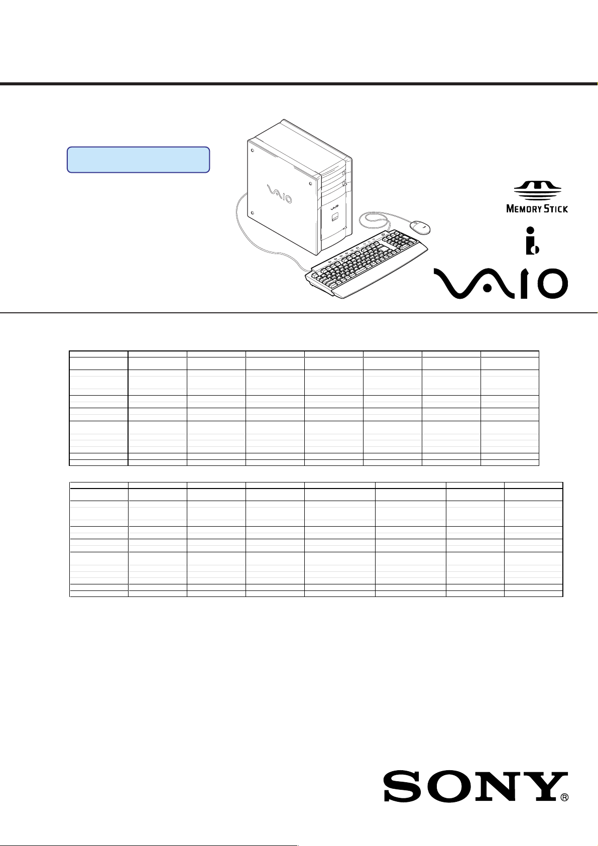
PCV-RX6
__
Series
SERVICE MANUAL
For American Area
US Model
Ver. 4-2002F
Canadian Model
Revision History
Lineup: PCV-RX640 PCV-RX671
PCV-RX650 PCV-RX672
PCV-RX660 PCV-RX681
PCV-RX670 PCV-RX682
PCV-RX680G PCV-RX651
PCV-RX690G PCV-RX641
PCV-RX600E
PCV-RX600N
Specifications
Model-name PCV-RX690G PCV-RX680G PCV-RX670 PCV-RX660 PCV-RX650 PCV-RX681 PCV-RX682
CPU
M/B (EE) (AN) (AN) (AN) (AN) (AN) (AN)
Memory std/max 512MB/1024MB 512MB/1024MB 512MB/1024MB 512MB/1024MB 512MB/1024MB 1024MB/1024MB 1024MB/1024MB
HDD Bay 1 120GB 120GB 80GB 80GB 80GB 120GB 120GB
Opt.Device Upper DVD-RW DVD-RW DVD-RW DVD-ROM DVD-ROM DVD-RW DVD-RW
Expansion Card
(Top) Slot4 (AGP) VGA Card VGA Card VGA Card VGA Card VGA Card VGA Card VGA Card
Slot3 (PCI) ---- Slot2 (PCI) MPEG ( ENX-17 ) MPEG ( ENX-17 ) - - (Bottom) Slot1 (PCI) Modem Modem Modem Modem Modem Modem Modem
MemoryStick aaaaaaa
OS Win XP Home Win XP Home Win XP Home Win XP Home Win XP Home Win XP Home Win XP Home
Slot 1 512MB 512MB 512MB 256MB/512MB 256MB / 512MB 512MB 512MB
Slot 2 (256MB CTO) None None 256MB/None 256MB / None 512MB 512MB
Bay 2 -----
Lower DVD-ROM CD-ROM CD-ROM CD-RW CD-RW CD-ROM DVD-ROM
P4 2.2GHz
P4 2.0AGHz
P4 1.8GHz P4 1.8GHz P4 1.6GHz P4 2.2GHz P4 2.2GHz
-
-
-
-
-
-
S400
Model-name PCV-RX671 PCV-RX672 PCV-RX640 PCV-RX600E PCV-RX600N PCV-RX651
CPU P4 2.0AGHz P4 2.0AGHz
M/B (AN) (AN) (BI) (EE) (AN) (AN)
Memory std/max 512MB/1024MB 512MB/1024MB 256MB/512MB 1024MB max 1024MB max
HDD Bay 1 120GB 120GB 60GB 60GB / 80GB / 120GB 60GB / 80GB / 120GB 80GB
Opt.Device Upper DVD-RW DVD-RW DVD-ROM DVD-RW / DVD-ROM DVD-RW / DVD-ROM DVD-ROM
Expansion Card
(Top) Slot4 (AGP) VGA Card VGA Card VGA Card VGA Card VGA Card VGA Card
Slot3 (PCI) - - Slot2 (PCI) (Bottom) Slot1 (PCI) Modem Modem Modem Modem Modem Modem
MemoryStick aa✕ aaa
OS Win XP Home Win XP Home Win XP Home Win XP Home
Slot 1 512MB 512MB 256MB 256MB / 512MB 256MB / 512MB 256MB 256MB
Slot 2 - -
Bay 2 - None / 120GB None / 120GB -
Lower CD-ROM DVD-ROM CD-RW DVD-ROM / CD-RW DVD-ROM / CD-RW CD-RW
--
-
- None / MPEG ( ENX-17 ) None / MPEG ( ENX-17 )
-
-
Cel 1.3GHz
- None / 256MB / 512MB None / 256MB / 512MB -
P4 1.6GHz / 1.8GHz / 2GHz /
2.2GHz(NW)
CTO Model CTO Model
P4 1.6GHz / 1.8GHz / 2GHz /
2.2GHz(NW)
Win XP Home / Win XP Professional
P4 1.7GHz
256MB/1024MB
-
-
Win XP Home
PCV-RX641
Cel 1.3GHz
(BI)
256MB/512MB
-
40GB
-
CD-RW
-
VGA Card
-
-
Modem
×
Win XP Home
PERSONAL COMPUTER VAIO
9-874-333-04
Information in this document is subject to change without notice.
CAUTION
Sony, VAIO and CLIE are trademarks or registered trademarks of
Sony. Microsoft, Windows, Windows Media, Outlook, Bookshelf
and other Microsoft products are trademarks or registered trademarks
of Microsoft Corporation in the United States and other countries.
The word Bluetooth and the Bluetooth logo are trademarks of
Bluetooth SIG, Inc. AMD, AMD logo, AMD Duron and
combinations thereof , 3DNow!, are trademarks of Advanced Micro
Devices, Inc. Intel Inside logo, Pentium and Celeron are trademarks
or registered trademarks of Intel Corporation.Transmeta, the
Transmeta logo, Crusoe Processor, the Crusoe logo and
combinations thereof are trademarks of Transmeta Corporation in
the USA and other countries. Graffiti, HotSync, PalmModem, and
Palm OS are resistered trademarks, and the Hotsync logo and Palm
are trademarks of Palm, Inc. or its subsidiaries. (M) and Motrola
are trademarks of Motrora, Inc. Other Motrola products and services
with (R) mark like Dragomball are the trademarks of Motrola, Inc.
All other names of systems, products and services in this manual
are trademarks or registered trademarks of their respective o wners.
In this manual, the (TM) or (R) mark are not specified.
Danger of explosion if battery is incorrectly replaced.
Replace only with the same or equivalent type
recommended by the manufacturer.
Dispose of used batteries according
to the manufacturer’s instructions.
Confidential
PCV-RX6__Series (AM)
– 2 –

TABLE OF CONTENTS
1. OPERATION
........................................................... 1-1
2. DISASSEMBLY
2-1. Flow Chart................................................................ 2-1
2-2. Top Panel Section .................................................... 2-2
2-3. Left Panel Section.................................................... 2-2
2-4. DVD-ROM, DVD-RW, CD-RW, CD-ROM............ 2-3
2-5. Switching Power ...................................................... 2-4
2-6. HDD ......................................................................... 2-5
2-7. PCI Slot Panel .......................................................... 2-5
2-8. VGA Card ................................................................ 2-6
2-9. Mounted PWB ENX-15........................................... 2-6
2-10. Modem Card ............................................................ 2-7
2-11. Panel Ass’y (Upper) (For 2 Bay)............................. 2-7
2-12. Panel Ass’y (Lower) (U).......................................... 2-8
2-13. Right Panel............................................................... 2-8
2-14. CNX-138 Board ....................................................... 2-9
2-15. CNX-137 Board ....................................................... 2-9
2-16. SWX-66 Board ........................................................ 2-10
2-17. FDD.......................................................................... 2-10
2-18. CNX-169/IFX-185 Board........................................ 2-11
2-19. Memory .................................................................... 2-12
2-20. CPU .......................................................................... 2-14
CPU Installation....................................................... 2-15
2-21. Mother Board ........................................................... 2-16
3. PROGRAMS FOR SERVICE
3-1. General ..................................................................... 3-1
3-2. PC-Doctor Starting Method..................................... 3-1
3-3. intel815E-B Video Diag Starting Method ............... 3-1
4. SERVICE INFORMATION
4-1. Jumper Setting on Hard Disk Drive ........................ 4-1
5. FRAME HARNESS
5-1. Connector List
1. Mother Board (BI) ................................................... 5-1
2. Mother Board (AN) ................................................. 5-4
3. Mother Board (EE) .................................................. 5-6
5-2. Frame Harness Diagram and Jumper Setting
of Mother Board ...................................................... 5-9
6. REPAIR PARTS LIST
6-1. Exploded Views and Parts List
(Mother Board (BI) Assy) ....................................... 6-1
6-2. Exploded Views and Parts List
(Mother Board (AN) Assy)...................................... 6-3
6-3. Exploded Views and Parts List
(Mother Board (EE) Assy)....................................... 6-5
6-4. Accessories and Parts List ....................................... 6-8
History of the changes is shown as the “Revision
History” at the end of this data.
– 3 –
Confidential
PCV-RX6__Series (AM)
2-1. FLOW CHART
SECTION 2
DISASSEMBLY
TOP PANEL
SECTION
P2-2
LEFT PANEL
SECTION
P2-2
DVD-ROM,
DVD-RW,
CD-RW,
CD-ROM
P2-3
SWITCHING
POWER
P2-4
HDD
P2-5
PCI SLOT
PANEL
P2-5
PANEL ASS’Y
(UPPER)
(FOR 2 BAY)
P2-7
FDD
P2-10
PANEL ASS’Y
(LOWER) (U)
P2-8
CNX-138
BOARD
P2-9
CNX-137
BOARD
P2-9
CNX-169/
IFX-185
BOARD
P2-11
RIGHT
PANEL
P2-8
SWX-66
BOARD
P2-10
MEMORY
P2-12
CPU
P2-14
MOTHER
BOARD
P2-16
VGA CARD
P2-6
MOUNTED PWB
ENX-15
P2-6
MODEM CARD
P2-7
•Ps-s denotes the page concerned.
• HDD has a low resistance to vibration, requiring careful handling.
2-1
Confidential
PCV-RX6__Series (AM)
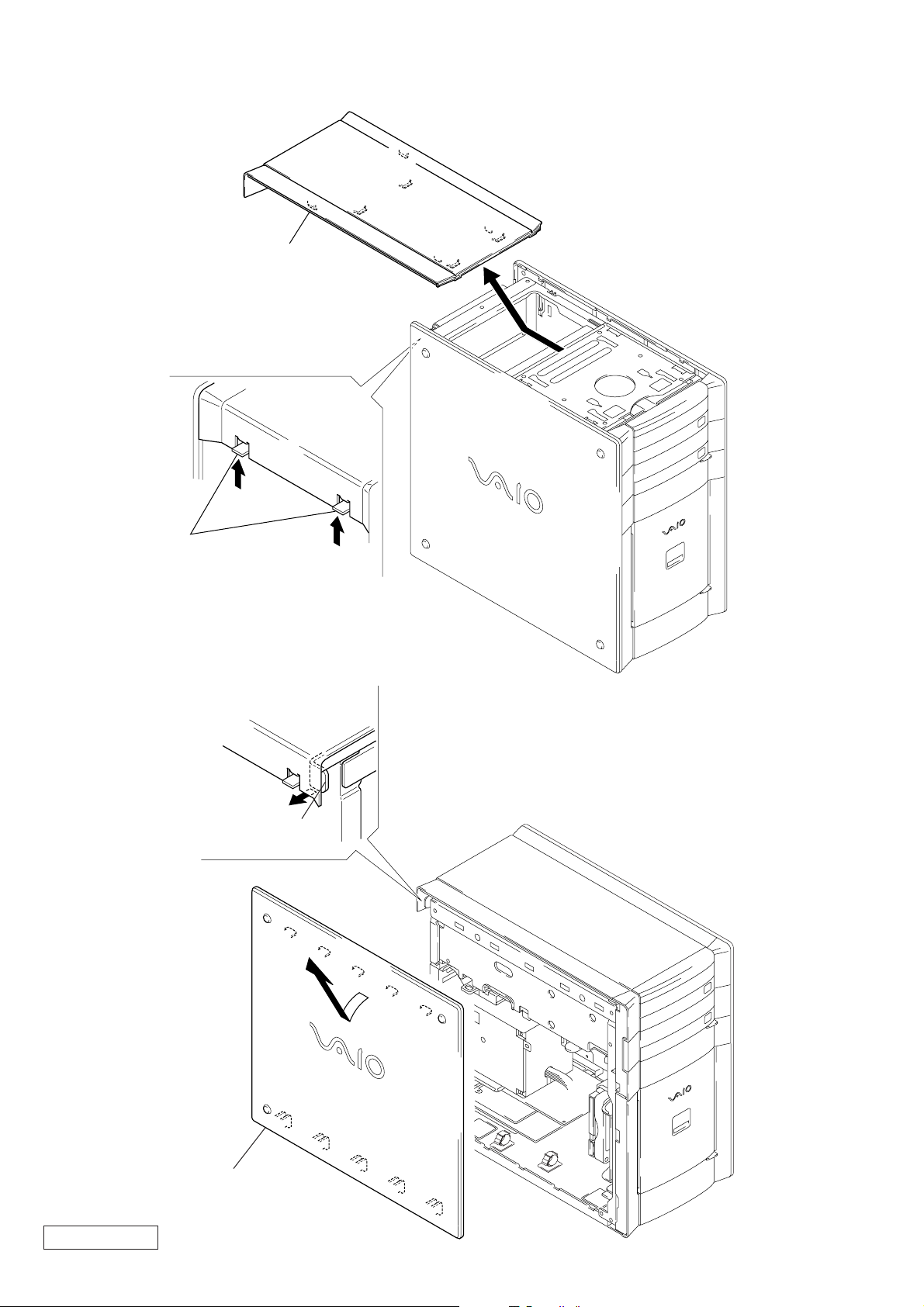
2-2. TOP PANEL SECTION
2
Remove the top panel section
in the direction of arrow
1
two claws
A
.
A
2-3. LEFT PANEL SECTION
1
Pull thelever.
A
2
Remove the left panel section
in the direction of arrow
Confidential
PCV-RX6__Series (AM)
A
.
2-2
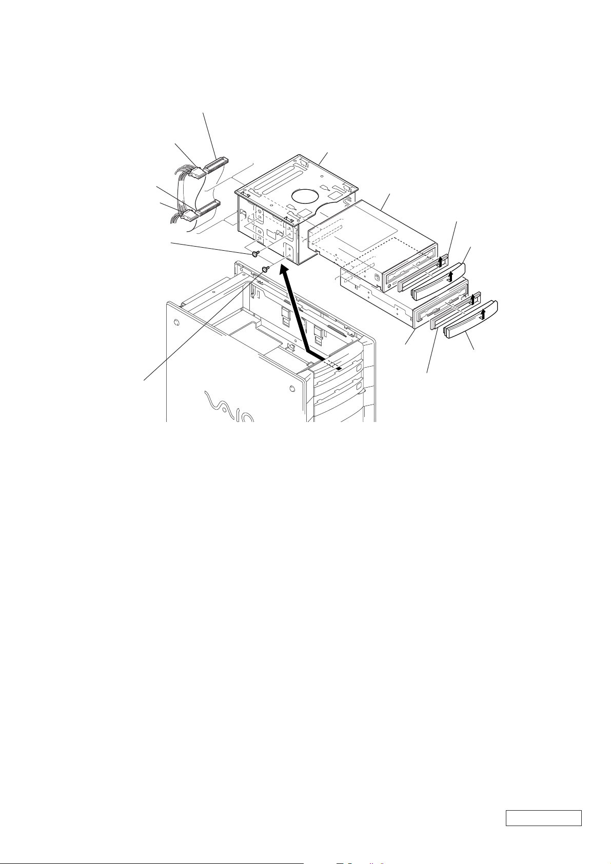
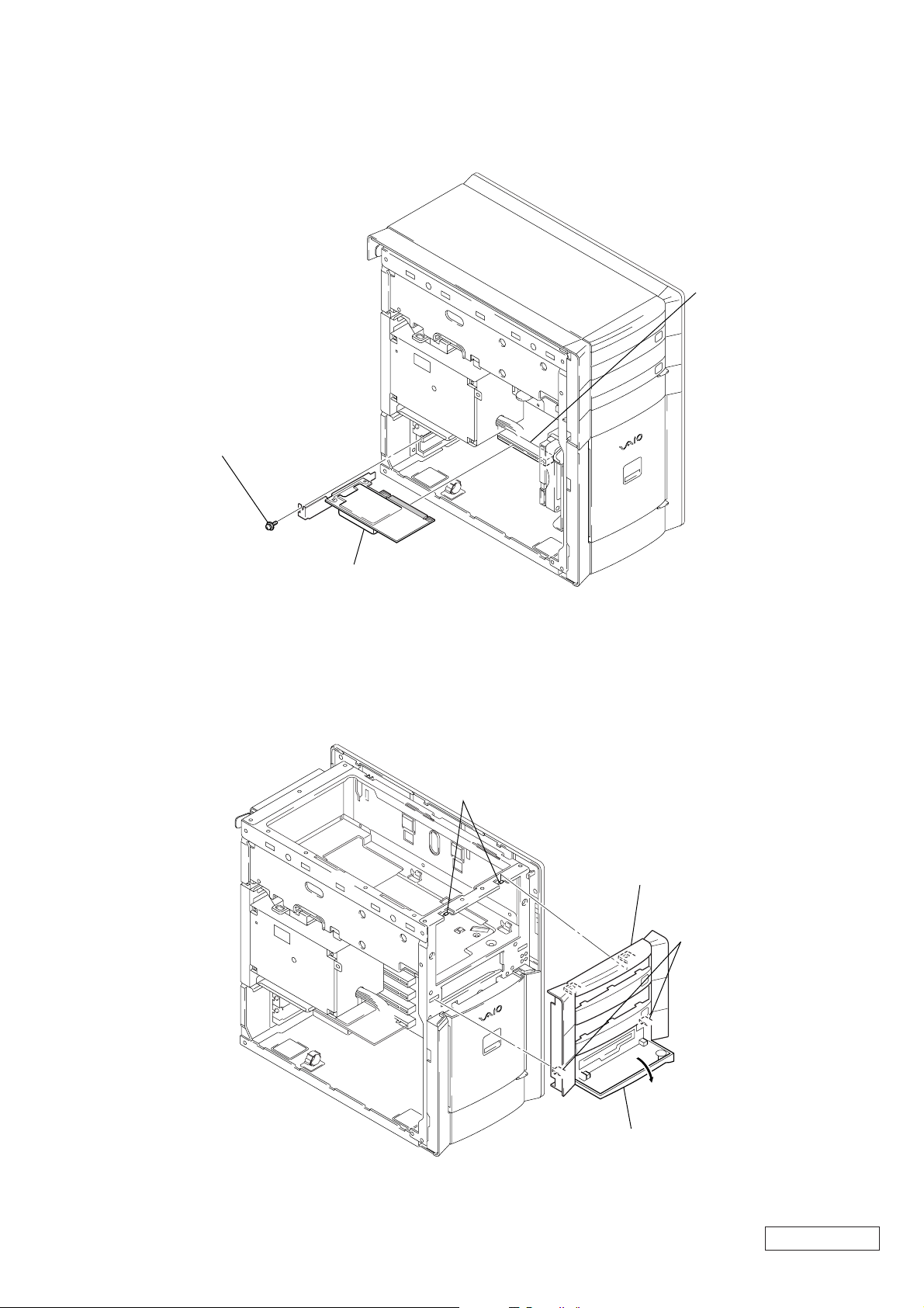
2-4. DVD-ROM, DVD-RW, CD-RW, CD-ROM
2
harness (IDE CD/DVD)
1
power connector
4
harness (IDE CD/DVD)
3
power connector
6
two screws
(PWH3
×
5)
5
Remove the CD holder ass’y
in the direction of arrow
7
DVD-ROM
DVD-RW
A
.
9
Remove the drive adaptor
in the direction of arrow
8
Remove the escutcheon
in the direction of arrow
C
C
.
B
.
0
two screws
(PWH3
A
qa
CD-RW
CD-ROM
qd
Remove the drive adaptor
×
5)
in the direction of arrow
B
E
D
Remove the escutcheon
qs
in the direction of arrow
E
.
D
.
2-3
Confidential
PCV-RX6__Series (AM)
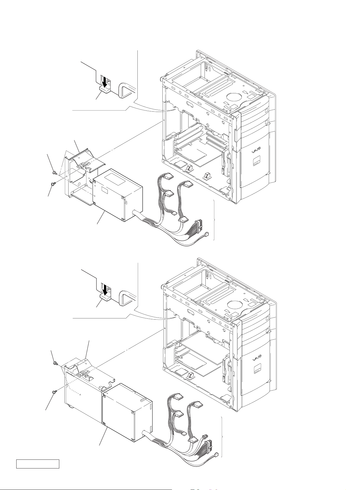
2-5. SWITCHING POWER
(1-468-417-72)
2
Push the lever.
3
bracket power
supply ass’y
5
three screws
(No.6-32UNC)
1
screw
(No.6-32UNC)
(1-468-601-14)
5
three screws
(No.6-32UNC)
6
switching power
2
Push the lever
3
bracket power supply ass’y
4
Disconnect respective
power connectors on the
mother board, DVD-ROM,
CD-RW, FDD and HDD.
1
screw
(No.6-32UNC)
Confidential
PCV-RX6__Series (AM)
6
switching power
2-4
4
Disconnect respective
power connectors on the
mother board, DVD-ROM,
DVD-RW, CD-RW, CD-ROM,
FDD and HDD.
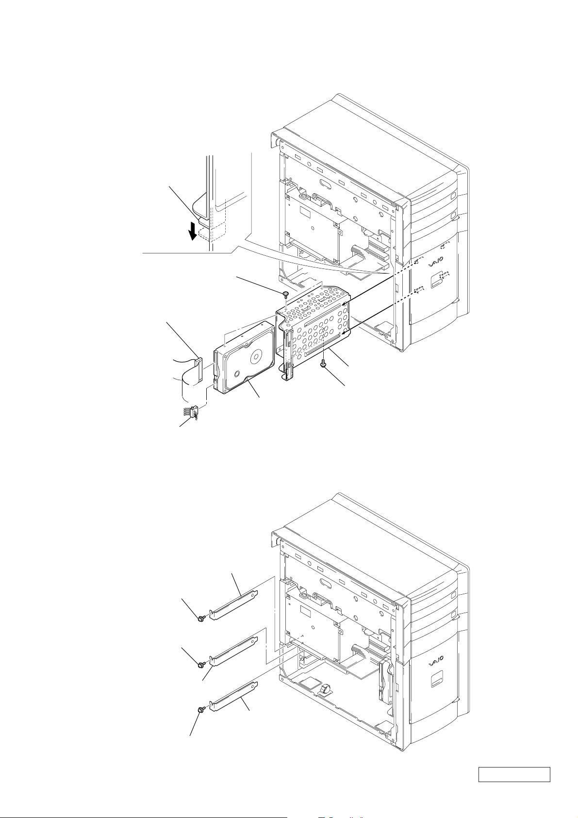
2-6. HDD
3
Push the lever.
1
harness
(IDE/ATA)
5
two screws
(SW) (No.6-32UNC)
2
power connector
2-7. PCI SLOT PANEL
1
screw
(SW) (No.6-32UNC)
3
screw
(SW) (No.6-32UNC)
2
PCI slot panel
6
HDD
4
HDD bracket ass’y
5
two screws
(SW) (No.6-32UNC)
4
PCI slot panel
5
screw
(SW) (No.6-32UNC)
6
PCI slot panel
2-5
Confidential
PCV-RX6__Series (AM)
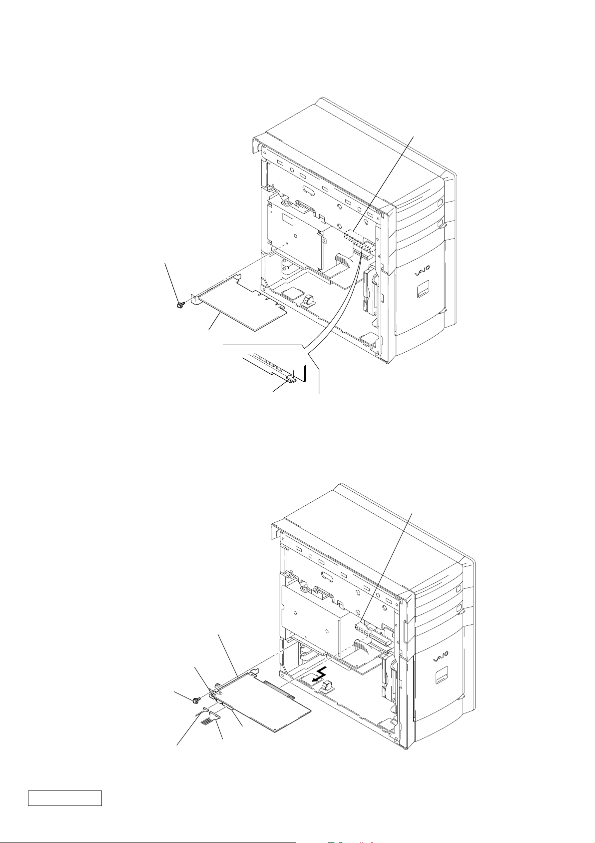
2-8. VGA CARD
1
screw
(SW) (No.6-32UNC)
3
AGP
VGA card
2-9. MOUNTED PWB ENX-15
4
3
screw
(SW) (No.6-32UNC)
2
Remove the mounted
PWB ENX-15 in the
direction of arrow
CN8
A
Push the clip.
PC12
.
A
Confidential
PCV-RX6__Series (AM)
2
harness
(audio)
CN9
1
harness (audio)
2-6
2-10. MODEM CARD
3
)
1
screw
(SW) (No.6-32UNC)
PCI
2
modem card
2-11. PANEL ASS’Y (UPPER) (FOR 2 BAY)
3
two claws
4
panel ass’y (upper) (for 2 bay
2
two claws
2-7
1
Open the door (FDD) ass’y.
Confidential
PCV-RX6__Series (AM)
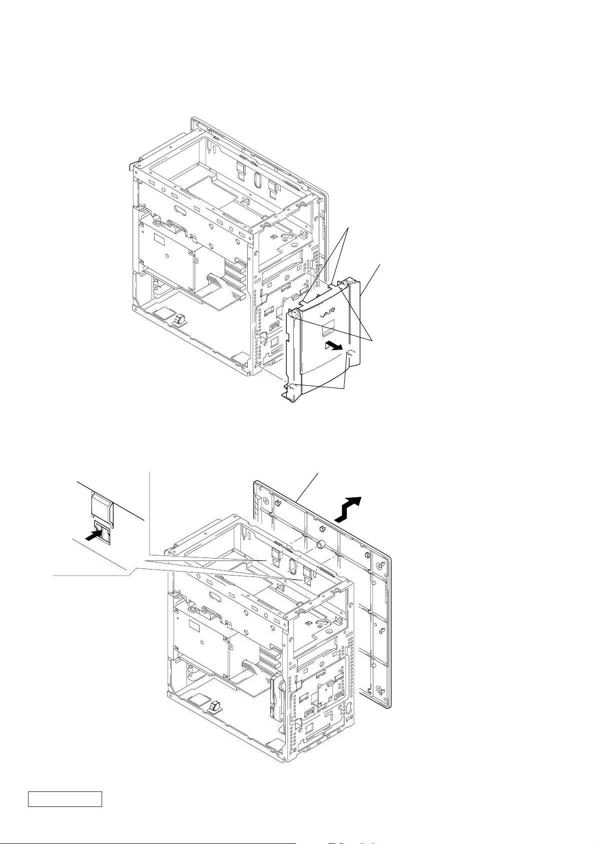
2-12. PANEL ASS’Y (LOWER) (U)
)
A
3
two claws
4
Remove the
front panel ass’y (lower) (U
in the direction of arrow A.
2
two claws
2-13. RIGHT PANEL
1
two claws
1
two claws
2
Remove the right panel
in the direction of arrow
A
A
.
Confidential
PCV-RX6__Series (AM)
2-8
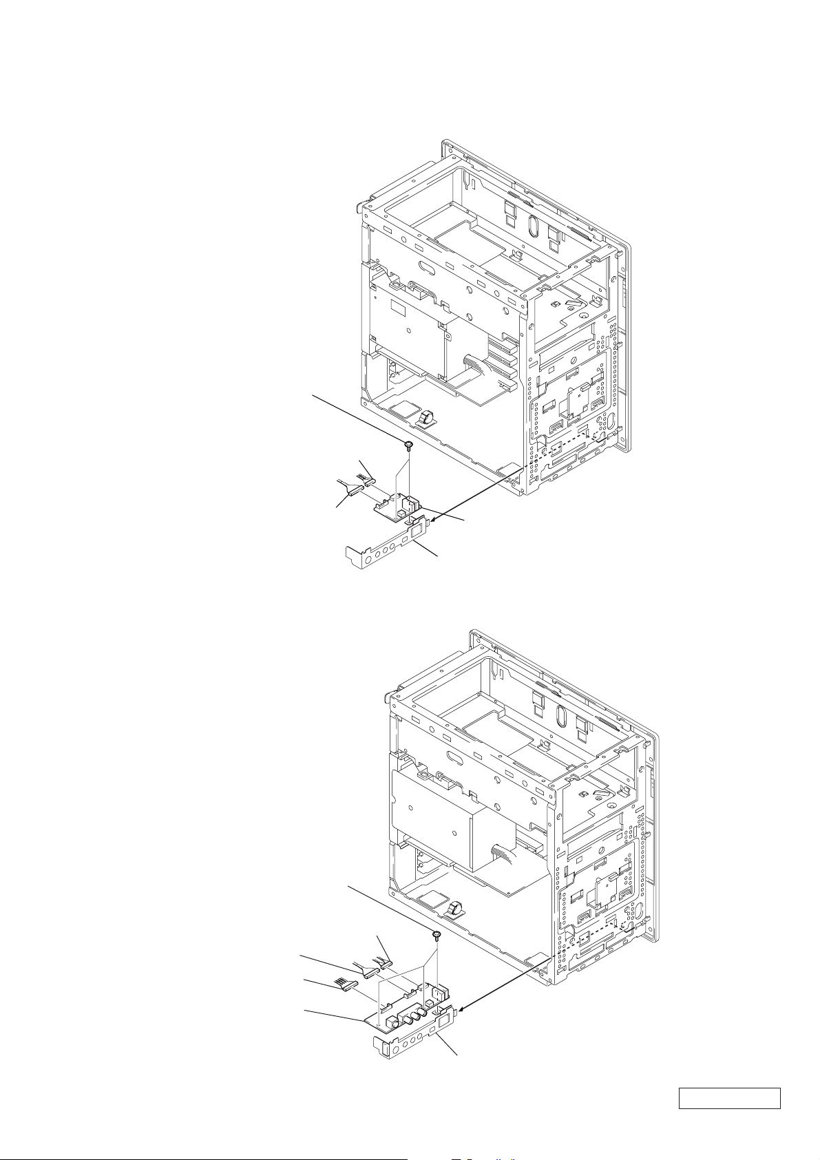
2-14. CNX-138 BOARD
4
two screws
(SW) (No.6-32UNC)
2
harness
(USB/LU)
1
harness
(1394)
A
5
CNX-138 board
2-15. CNX-137 BOARD
5
three screws
(SW) (No.6-32UNC)
2
harness
(1394)
3
harness
(USB/LU)
3
Remove the bracket AV ass’y
in the direction of arrow
A
.
1
harness (AUDIO)
6
CNX-137 board
2-9
A
4
Remove the bracket AV ass’y
in the direction of arrow
A
.
Confidential
PCV-RX6__Series (AM)

2-16. SWX-66 BOARD
)
4
LED shield
3
SWX-66 board
1
harness
(SW/LED)
2
screws
(SW) (No.6-32UNC
2-17. FDD
3
1
harness (FDD)
Push the lever.
4
Remove the FDD
bracket ass’y in the
direction of arrow
2
harness
A
.
A
Confidential
PCV-RX6__Series (AM)
5
two screws
(PWH3
×
5)
6
FDD
2-10

2-18. CNX-169/IFX-185 BOARD
3
CNX-169/
IFX-185 board
1
two screws
(SW) (No.6-32UNC)
2
claw
2-11
Confidential
PCV-RX6__Series (AM)

2-19. MEMORY (DIMM)
2
memory (DIMM) × 2
Note 1: In opening the clips,
hold lightly the top of the memories
with your fingers to prevent a drop.
Note 2: In removing the memories,
always start from the one
having largest bank number.
1
Open two clips.
1
Open two clips.
(RIMM, CRIMM)
4
memory (RIMM) × 2
Note 1: In opening the clips,
hold lightly the top of the memories
with your fingers to prevent a drop.
Note 2: In removing the memories,
always start from the one
having largest bank number.
2
RIMM × 2
or CRIMM × 2
1
3
Open two clips.
3
Open two clips.
1
Open two clips.
Open two clips.
Confidential
PCV-RX6__Series (AM)
2-12

(DDR)
2
memory (DDR) × 2
Note 1: In opening the clips,
hold lightly the top of the memories
with your fingers to prevent a drop.
Note 2: In removing the memories,
always start from the one
having largest bank number.
1
Open two clips.
1
Open two clips.
2-13
Confidential
PCV-RX6__Series (AM)

2-20. CPU
2
4
Elect the lever
in the direction of arrow
clip
5
A
.
CPU
1
harness
AA
2
3
DC fan
(with heat sink)
clip
3
DC fan
(with heat sink)
5
CPU
1
harness
A
2
Confidential
PCV-RX6__Series (AM)
clip
4
Elect the lever
in the direction of arrow
2-14
A
.

• CPU INSTALLATION
Note : When heat sink is removed from CPU,
Thermal diffusion grease : silicon compound (G-765) 90G
Amount to apply : 0.1 g (as the same size as the tip of a match) (Celeron)
install new ones after thermal diffusion
grease is wiped off and silicon compound
is applied to the place shown in the figure.
0.5 g (as the same size as the tip of a match) (Pentium 4)
(Celeron) (Pentium 4)
grease
(in the surface at the
splatter)
Take care not to apply the grease
*
to any other places because it has
high conductivity.
grease
(in the surface at the
splatter)
2-15
Confidential
PCV-RX6__Series (AM)

2-21. MOTHER BOARD
7
1
harness
(MS, SIO)
2
harness
(IDE CD/DVD)
harness
(1394)
3
harness
(IDE/ATA)
5
harness
(USB/LU)
4
harness
(FDD)
6
harness (SW/LED)
Confidential
PCV-RX6__Series (AM)
9
Remove the mother board
to direction of arrow
8
eight screws
(SW) (No.6-32UNC)
A
.
A
2-16
(END)

SECTION 3
PROGRAM FOR SERVICE
3-1. General
The Diagnostic Programs for Service are available with the following three kinds.
1. PC-Doctor
This can test the Mother Board, CPU, Memory, FDD, HDD, and
Optical drive.
2. intel815E-B Video Diag
This can test the VGA (intel815E-B Chipset built in).
3. nVIDIA Video Diag
There are two types of diagnostic programs, one for the memory
Geforce2Ti (64M) and TNT2M64 (32M).
3-2. PC-Doctor Starting Method
As the Diag. disc is a bootable CD, set the CD in the Optical drive
and turn the system power on.
The menu will be displayed, then select the menu.
1. PC-Doctor
After the system started, set a DOS formatted 1.44M floppy disk
without the write protection in the FDD, and the CD-ROM Disc in
the Optical drive, select the model to be tested following the menu.
All tests are carried out automatically.
Do not remove the Diag. disc during the test.
DISKETTE TEST
FDD is tested.
As the read/write operation is performed to the floppy disk,
set the DOS formatted 1.44M disk without the write protection before the PC-Doctor is started. Also, if the PC-Doctor is
booted from the CD, the boot image of CD is treated as the
floppy 0 (drive A), and accordingly the FDD is treated as the
floppy 1 (drive B).
In this case, the floppy 0 cannot be tested and N/A is displayed
as the test result, but this is not a fault.
MISCELLANEOUS TEST
Other devices are tested.
CD/DVD-ROM read check, CPU type check, and configuration check of PCI device, etc. are executed.
3-2-2. Test Result
After the test finished, “PASSED” or “FAILED” is displayed.
In case of “FAILED” display, press the F1 key to display the log
and then, check the faulty item.
Certain items cannot be tested and N/A is displayed, but this is not
a fault.
Example of log file
PC-DOCTOR 2.0 SYSTEM TEST LOG
=================================
Inventory........................
CPU MHz is too low (700 vs 750)
Inventory FAILED
3-2-1. Test Items
CPU/COPROCESSOR TEST
The CPU/Coprocessor are tested.
MEMORY TEST
The memory is tested.
The bus throughput of the extended memory cannot be tested,
and therefore N/A is displayed as the test result, but this is not
a fault.
SYSTEM BOARD TEST
The Mother Board is tested.
Also, the keyboard and mouse are tested, thus requiring the
keyboard and mouse to be connected to the set in advance.
SERIAL PORT TEST
The COM port is tested.
PARALLEL PORT TEST
The printer port is tested.
VIDEO ADAPTER TEST
The video card is tested.
Only the DOS legacy mode is tested.
FIXED DISK TEST
HDD is tested.
3-3. intel815E-B Video Diag Starting Method
As the Diag. disc is a bootable CD, set the CD in the Optical drive
and turn the system power on.
The menu will be displayed, then select the following:
2. intel815E-BVideo Diag
After the system started, the file is automatically expanded on the
RAM disk and the test starts.
3-3-1. Test Result
After the test finished, “PASS” or “FAIL” is displayed.
The contents of RAM disk are cleared when the power is turned
off.
3-4. nVIDIA Geforce Video Diag Starting Method
As the Diag. disc is a bootable CD, set the CD in the Optical drive
and turn the system power on.
The menu will be displayed, then select the menu.
After the system started, the file is automatically expanded on the
RAM disk and the test starts.
3-4-1. Test Result
After the test finished, “PASS” or “FAIL” is displayed.
The contents of RAM disk are cleared when the power is turned
off.
3-1
(END)
Confidential
PCV-RX6__Series (AM)

SECTION 4
SERVICE INFORMATION
4-1. JUMPER SETTING ON HARD DISK DRIVE
The hard disk drive of service parts can be used without changing factory jumper setting, when it was replaced for service.
Part No. Maker Code
Capacity
(formatted)
A-8110-897-A Seagate ST340810A 40 GB
A-8025-545-A Seagate ST360020A 60 GB
A-8058-425-A Seagete ST380020A 80 GB
17
28
Configuration Jumper Setting
Limit capacity
>32 Gbytes = 32 Gbytes
<32 Gbytes = 2.1 Gbytes
Master or single drive
Drive is a slave
Master with a non-ATA
compatible slave
Enable cable select
Memo
Part No. Maker Code
Capacity
(formatted)
A-8059-699-A Maxtor 4G120J6 120 GB
Master/Slave selection
Jumper setting
J42 Factory Reserved
J44 Factory Reserved
J46 Cylinder Limitation
J48 Cable Select
J50 Master/Slave
Configuration Jumper Settings
Only drive in single drive system
Master drive in dual drive system
Slave drive in dual drive system
Memo
4-1
(END)
Confidential
PCV-RX6__Series (AM)

5-1. CONNECTOR LIST
FDD
Connector location on MB See the frame harness daigram
Pin assignments:
Pin Signal Name Pin Signal Name
1Ground 2 HDsel
3Ground 4 N.C.
5Ground 6 DRIVE_SELECT_#3
7Ground 8 INDEX
9Ground 10 DRIVE_SELECT_#0
11 Ground 12 DRIVE_SELECT_#1
13 Ground 14 DRIVE_SELECT_#2
15 Ground 16 N.C.
17 Ground 18 DIRECTION#
19 Ground 20 STEP#
21 Ground 22 WRITE_DATA#
23 Ground 24 WRITE_GATE#
25 Ground 26 TRACK_00#
27 Ground 28 WRITE_PROTECT#
29 N.C. 30 READ_DATA#
31 Ground 32 SIDE_1_SELECT#
33 N.C. 34 DSKCHG#
--NOTE-'HDsel' signal is sent form drive. It indicate 2HD(when High) or 2DD(when Low) media.
'MODE_SELECT#' is control signal of disk rotation speed. When this signal is High,
Media rotates 300RPM (2MB). When Low, media rotates 360RPM(1.6MB).
168pin DIMM socket x2
2 slot DIMM connector, 3.3V Unbuffered SDRAM
Connector location on MB See the frame harness daigram
PGA370 socket
Coppermine-128k, Coppermine-256K , Tualatin-128K, Tualatin-256K supported
Connector location on MB See the frame harness daigram
AGP Slot
Single Edge Contact AGP slot. Universal AGP connector with AGP card lock system.
Connector location on MB See the frame harness daigram
CPU FAN
Supports CPU cooling fan of 500mA or less. Voltage = 12V
Connector location on MB See the frame harness daigram
Pin assignments:
Pin Signal Name
1 Ground
2FAN_CTRL (+12 V)
3FAN_SEN
Fan control circuit is same as Eeth MB and Anakin MB.
Chassis FAN ( Option )
Supports Chassis cooling fan of 500mA or less. Voltage = 12V
Connector lo cation on MB See
the frame h arness diagram
Pin assignments:
Pin Signal
Name
1Ground
2 FAN_CTRL (+12 V)
3 FAN_SEN
Fan control circuit is same as Eeth MB and Anakin MB.
1. MOTHER BOARD (BI)
1-1 Internal connector
Power supply
20pin ATX type connector.
Connector location on MB See the frame harness daigram
Pin assignments:
Pin Signal Name
1 +3.3 V
2 +3.3 V
3Ground
4 +5 V
5Ground
6 +5 V
7Ground
8PWRGD (Power Good)
9 +5 VSB
10 +12 V
11 +3.3 V
12 -12 V
13 Ground
14 PS-ON# (power supply remote on/off control)
15 Ground
16 Ground
17 Ground
18 No Connection
19 +5 V
20 +5 V
PS FAN
Support FAN control of power supply.
Connector location on MB See the mechanical drawing sheet
Pin assignments:
Pin Signal Name
1Ground
2FAN_CTRL (0V(S3) , 2V(S1), 12 V(S0))
3FAN_SEN
The FAN_CTRL line is controlled by the BIOS and this line is voltage control line
Fan control circuit is same as Eeth MB and Anakin MB.
IDE Primary / Secondary
For 3.5'' Hard Drive, 40 pin Header (2.54mm standard type)
Connector location on MB See the frame harness daigram
Host side detect Cable Type Using GPIOs
SECTION 5
FRAME HARNESS
PCI Slot x3
Single Edge Contact PCI slot.
Connector location on MB See the mechanical drawing sheet
-12V B1 A1 TRST# AD[17] B32 A32 AD[16]
TCK B2 A2 +12V C/BE[2]# B33 A33 +3.3V
Ground B3 A3 TMS Ground B34 A34 FRAME#
TDO B4 A4 TDI IRDY# B35 A35 Ground
+5V B5 A5 +5V +3.3V B36 A36 TRDY#
+5V B6 A6 INTA# DEVSEL# B37 A37 Ground
INTB# B7 A7 INTC# Ground B38 A38 STOP#
INTD# B8 A8 +5V LOCK# B39 A39 +3.3V
PRSNT1# B9 A9 Reserved PERR# B40 A40 Reserved
Reserved B10 A10 +5V +3.3V B41 A41 Reserved
PRSNT2# B11 A11 *Reserved SERR# B42 A42 Ground
Ground B12 A12 Ground +3.3V B43 A43 PAR
Ground B13 A13 Ground C/BE[1]# B44 A44 AD[15]
Reserved B14 A14 Reserved AD[14] B45 A45 +3.3V
Ground B15 A15 RST# Ground B46 A46 AD[13]
CLK B16 A16 +5V AD[12] B47 A47 AD[11]
Ground B17 A17 GNT# AD[10] B48 A48 Ground
REQ# B18 A18 Ground Ground B49 A49 AD[09]
+5V B19 A19 Reserved Key B50 A50 Key
AD[31] B20 A20 AD[30] Key B51 A51 Key
AD[29] B21 A21 +3.3V AD[08] B52 A52 C/BE[0]#
Ground B22 A22 AD[28] AD[07] B53 A53 +3.3V
AD[27] B23 A23 AD[26] +3.3V B54 A54 AD[06]
AD[25] B24 A24 Ground AD[05] B55 A55 AD[04]
+3.3V B25 A25 AD[24] AD[03] B56 A56 Ground
C/BE[3]# B26 A26 IDSEL Ground B57 A57 AD[02]
AD[23] B27 A27 +3.3V AD[01] B58 A58 AD[00]
Ground B28 A28 AD[22] +5V B59 A59 +5V
AD[21] B29 A29 AD[20] ACK64# B60 A60 REQ64#
AD[19] B30 A30 Ground +5V B61 A61 +5V
+3.3V B31 A31 AD[18] +5V B62 A62 +5V
PCI #3 slot has special connection at A11 pin.
The serial IRQ signal connects to the A11 pin on the PCI #3.
5-1
Confidential
PCV-RX6__Series (AM)

CD audio
4 pin standard 2mm single line header for CD Audio signal input
Connector location on MB See the frame harness daigram
Pin assignments:
Pin Signal Name
1Left Line In
2 Ground
3 Ground
4 Right Line In
AUX Audio (not installed*)
4 pin standard 2mm single line header for AUX Audio signal input
Connector location on MB See the frame harness daigram
Pin assignments:
Pin Signal Name
1Left Line In
2Ground
3Ground
4Right Line In
Video Audio (not installed*)
4 pin standard 2mm single line header for Video Audio signal input
Connector location on MB See the frame harness daigram
Pin assignments:
Pin Signal Name
1Video_L
2Ground
3Ground
4Video_R
I/O header
20 pin standard 2.5mm dual line header f or LED/Switch unit
Connector location on MB See the frame harness daigram
Pin assignments:
PinSignal Name Pin Signal Name
1PWR_BTN 11 MSG_LED+
2PWR_BTN_G 12 MSG_LED3IDELED- 13 KEYLOCK
4IDELED+ 14 KEYLO CK_G
5KEY 15 SMI
6PWR_LEDL+ 16 SMI_G
7PWR_LED- 17 +5V
8PWR_LEDB+ 18 HD_LED29RESET 19 Ground
10 RESET G (GND) 20 SPKR
Battery Holder & Battery
Holder location on MB See the frame harness daigram
Thermal measurement header
This header is used for thermal measurem ent at evaluation stage.
This connector does not need at produc tion board.
This signal also routed to Super I/O for thermal monitoring.
3pin standard 2mm single line header for CPU thermal measurement
Connector location on MB See the frame harness daigram
Pin assignments:
PinSignal Name
1THERMDP ( CPU B14 )
2THERMDN ( CPU B15 )
3Ground
SPDIF OUT (Option)
3 pin standard 2mm single line header for SPDIFoutput
Connector location on MB See the frame harness daigram
Pin assignments:
Pin Signal Name
1 VCC
2AU_DATA(GPIO[2])
3Ground
IEEE1394 access header x2
8 pin standard 2.5 mm single line header f or IEEE1394 Front connector.
Connector location on MB See the frame harness daigram
Pin assignments:
PinSignal Name
1Shell Ground
2Ground
3TPA
4TPA*
5TPB
6TPB*
7Ground
8VP ( Power )
VP line need over current protector. Raychem SMD150/ 33-2 or equivalent is used for that.
USB Front access header
16 pin standard 2.5mm Dual line Box header for Front USB connector.
Connector location on MB See the frame harness diagram
Pin assignments:
PinSignal Name Pin Signal Name
1USB VCC1 2 USB VCC3
3P1-4P35P1+6P3+
7GND8GND
9KEY10GND
11 CP2- 12 P213 CP2+ 14 P2+
15 NC 16 USB VCC3
USBVCC2 and USBVCC3 line needs the over current protector.
Raychem miniSMDC110-2 or equivalent is used for that.
1-2 External connector
Parallel
Connector location on MB Rear side, see the frame harness daigram
Pin assignments:
PinSignal Name Pin Signal Name
1Strobe# 14 Auto Feed#
2Data bit 0 15 Fault#
3Data bit 1 16 INIT#
4Data bit 2 17 SLCT IN#
5Data bit 3 18 Ground
6Data bit 4 19 Ground
7Data bit 5 20 Ground
8Data bit 6 21 Ground
9Data bit 7 22 Ground
10 ACK# 23 Ground
11 Busy 24 Ground
12 Error 25 Ground
13 Select
VGA
Connector location on MB Rear side, see the frame harness daigram
Pin assignments:
PinSignal Name
1RED
2GREEN
3BLUE
4NC
5GND
6GND
7GND
8GND
9Reserved
10 GND
11 NC
12 DDCDAT
13 HSYNC
14 VSYNC
15 DDCCLK
Confidential
Connectors mentioned (not installed) are not
*
used even they are mounted on MB.
5-2PCV-RX6__Series (AM)

IEEE1394 Rear connector
6 pin standard IEEE1394 Rear co nnector.
Connector location on MB See the frame harness daigram
Pin assignments:
PinSignal Name
1 VP (Power )
2Ground
3TPB*
4TPB
5TPA*
6TPA
Line In pin assignments:
PinSignal Name
Sleeve Ground
Tip Audio Left In
Ring Audio Right In
Microphone In pin assignments:
PinSignal Name
Sleeve Ground
TipMicrophone mono In
Ring Electret Bias Voltage
VP line need over current protector.
Raychem SMD150/33-2 or equivalent is used for that.
PS2 Keyboard /Mouse
Connector location on MB Rear side, see the frame harness daigram
Pin assignments:
PinSignal Name
1Keyboard Data
2Mouse Data
3Ground
4PS2VCC
5Keyboard Clock
6Mouse Clock
7Mouse Data
8N.C.
9Ground
10 PS2VCC
11 N.C.
12 Mouse Clock
PS2VCC line needs the over current protector. Raychem miniSMDC110-2 or equivalent is u
sed for that.
USB/LAN
Two USB connector for external USB devices. (Support the stacked connector)
One 10/100Base-T connector
Connector location on MB See the frame harness daigram
Pin assignments:
PinSignal Name
1USBVCC1
2USBP0#
3USBP0
4Ground
5USBVCC2
6USBP1#
7USBP1
8Ground
9
10
11
12
13
14
15
16
USBVCC1/USBVCC2 lines need the over current protector.
Raychem miniSMDC110-2 or equival ent is used for that.
1-3 Jumper Header
CPU Clock select
Jumper Header manual conf ig uration i s us ed onl y for debug.
Production should be auto-sense configuration. PCB should be able to suppor
t automatic and manual configuration by minimal mount options.
Select CPU's External frequency (BUS frequency) and BUS Frequency Multipl
ier and Memory Frequency. (Acceptable for BIOS setting instead of Jumper H
eader)
CMOS Clear/Reboot En
Clear the RTC data
Connector location on MB See the frame harness daigram
Jumper header
1 2 3
Combination of jumper caps:
CMOSCLR RBT_EN
1-2 Normal Reboot Disabled
2-3 Clear Normal
Reboot Enable:
If set to 1-2, disables reboot function
This header is for factory testing purpose only
DO NOT CHANGE
1-4 USB Routing Layout
Same routing as Eeth MB and Adi MB.
Lower Side of USB CON
USB
CON
Upper Side of
USB CON
Port1
ICH
CUSL-LV
Rev 1.0x
Port3
Port2
COM/Line Out/Line In/Microphone Jack
Connector location on MB Rear side, see the frame harness daigram
COM1 pin assignments:
PinSignal Name
1 DCD
2Serial In #
3Serial Out #
4DTR#
5Ground
6DSR
7RTS
8CTS
9RI1#
Line Out pin assignments:
COM1, COM2 RI# output conn
ected to ICH input for Wakeup
event
PinSignal Name
Sleeve Ground
Tip Audio Left Out
Ring Audio Right Out
5-3
Default setting of Port3 is disable by NP3 (High)
Confidential
PCV-RX6__Series (AM)

2. MOTHER BOARD (AN)
CD audio
4 pin standard 2mm single line header for CD Audio signal input
Connector location on MB See the frame harness diagram
Pin assignments:
PinSignal Name
1Left Line In
2Ground
3Ground
4Right Line In
2-1 Internal connector
Power supply
20 pin ATX type connector.
Connector location on MB See the frame harness diagram
4 pin ATX12V type connector.
Connector location on MB See the frame harness diagram
PS FAN
Support FAN control of power supply.
Connector location on MB See the frame harness diagram
Pin assignments:
PinSignal Name
1Ground
2FAN_CTRL (0V(S3) , 2V(S1), 12 V(S0))
3FAN_SEN
The FAN_CTRL line is controlled by the BIOS and this line is voltage control line
IDE Primary / Secondary
For 3.5'' Hard Drive, 40 pin Header (2.54mm standard type)
Connector location on MB See the frame harness diagram
Host side detect Cable Type Using GPIOs
FDD
Connector location on MB See the frame harness diagram
168pin DIMM socket x 2
2 slot DIMM connector, 3.3V un-buffered SDRAM
Connector location on MB See the frame harness diagram
mPGA478socket
Intel Pentium4 supported
Connector location on MB See the frame harnes s diagram
PCI Slot x3
Single Edge Contact PCI slot
Connector location on MB See the frame harnes s diagram
PCI #3 slot has special connection at A11 pin.
The serial IRQ signal connects to the A 11 pin on the PCI #3.
AGP Slot
Single Edge Contact AGP slot. 1.5V AGP connector with retention mechanism
Connector location on MB See the frame harness diagram
CPU FAN
Supports CPU cooling fan of 500mA or less. Voltage = 12V
Connector location on MB See the frame harness diagram
Pin assignments:
PinSignal Name
1Ground
2FAN_CTRL (+12 V)
3FAN_SEN
Wake On LAN (not installed*)
Support Wake On LAN function
Connector location on MB See the frame harness diagram
Pin assignments:
PinSignal Name
1+5Vsb
2Ground
3WOL signal
Confidential
AUX A udio
4 pin standard 2mm single line header for AUX Audio signal input
Connector location on MB See the frame harness diagram
Pin assignments:
PinSignal Name
1Left Line In
2Ground
3Ground
4Right Line In
Video Audio (not installed*)
4 pin standard 2mm single line header for AUX Audio signal input
Connector location on MB See the frame harness diagram
Pin assignments:
PinSignal Name
1Left Line In
2Ground
3Ground
4Right Line In
IEEE1394 access header x2
8 pin standard 2.5mm single line header for IEEE1394 Front connector.
Connector location on MB See the frame harness diagram
Pin assignments:
PinSignal Name
1Shell Ground
2Ground
3TPA
4TPA*
5TPB
6TPB*
7Ground
8VP (Power)
VP line need over current protector. Raychem SMD150/33-2 or equivalent is used for that.
USB Front access header
16 pin standard 2.5mm Dual line Box header for Front USB connector.
Connector location on MB See the frame harness diagram
Pin assignments:
PinSignal Name Pin Signal Name
1USB VCC1 2 USB VCC3
3P1-4P35P1+6P3+
7GND8GND
9KEY10GND
11 CP2- 12 P213 CP2+ 14 P2+
15 NC 16 USB VCC3
USBVCC2 and USBVCC3 line nee ds t he ov er current protector.
Raychem miniSMDC110-2 or equival ent is used for that.
Connectors mentioned (not installed) are not
*
used even they are mounted on MB.
5-4PCV-RX6__Series (AM)

I/O header
2
3
20 pin standard 2.5mm dual line header for LED/Switch unit
Connector location on MB See the frame harness diagram
Pin assignments:
PinSignal Name Pin Signal Name
1PWR_BTN 11 MSG_LED+
2PWR_BTN_G 12 MSG_LED3IDELED- 13 KEYLOCK
4IDELED+ 14 KEYLOCK_G
5KEY 15 SMI
6PWR_LEDL+ 16 SMI_G
7PWR_LED- 17 +5V
8PWR_LEDB+ 18 HD_LED29RESET 19 Ground
10 RESET G (GND) 20 SPKR
Battery Holder
Holder location on MB See the frame harness diagram
USB/LAN
One USB connectors for external USB devices (Support the stacked connector)
One 10/100Base-T connector
Connector location on MB See the frame harness diagram
Pin assignments:
PinSignal Name Pin Signal Name
1ACTLEDP 11 LANP8
2ACTLEDN 12 LANP8
3LILEDP 13 USBVCC1
4LILEDN 14 USBP1-
5TXPCON 15 UCBP1+
6TXNCON 16 GND
7RXPCON 17 NC
8LANP5 18 NC
9LANP5 19 NC
10 RXNCON 20 NC
USBVCC1 lines need the over current protector.
Raychem miniSMDC110-2 or equivalent is used for that.
CPU thermal measurement header
header is used for CPU thermal measurement.
This
This signal also routed to Super I/O for thermal monitoring.
2pin standard 2mm single line header for CPU thermal measurement
Connector location on MB See the frame harness diagram
Pin assignments:
Pin Signal Name
1 CPUTMPIN
2GND
Memory Stick interface header
8pin standard 2mm dual line header for Memory Stick interface.
Pin assignments:
Pin Signal Name
1 MS_LED
2 MSPIN2
3 SONYMSP
4 MSPIN4
5 MS_INS
6 GND
7 MSPIN7
8 GND
2-2 External connector
Parallel
Connector location on MB Rear side, See the frame harness diagram
IEEE1394 Rear connector
6 pin standard IEEE1394 Rear connector.
Connector location on MB See the frame harness diagram
Pin assignments:
Pin Signal Name
1 VP (Power)
2Ground
3 TPB*
4 TPB
5 TPA*
6 TPA
VP line need over current protector.
Raychem SMD150/33-2 or equivalent is used for that.
COM1 Port/Line Out/Line In/Microphone Jack
Connector location on MB Rear side, See the frame harness diagram
2-3 Jumper Header
CMOS Clear
Clear the RTC data
Connector location on MB ---
Jumper header
1
Combination of jumper caps:
1-2 Clear
2-3 Normal
CMOSCLR
PS2 Keyboard /Mouse
Connector location on MB Rear side, See the frame harness diagram
PS2VCC line needs the over current protector. Raychem miniSMDC110-2 or equivalent is
used for that.
Confidential
5-5
PCV-RX6__Series (AM)

3. MOTHER BOARD (EE)
See the frame harness diagram
See the frame harness diagram
See the frame harness diagram
See the frame harness diagram
See the frame harness diagram
3-1 Internal connector
Power supply
20 pin ATX type connector.
Connector location on MB See the frame harness diagram
4 pin ATX12V type connector.
Connector location on MB See the frame harness diagram
PS FAN
Support FAN control of power supply.
Connector location on MB See the frame harness diagram
Pin assignments:
Pin Signal Name
1Ground
2FAN_CTRL (0V(S3) , 2V(S1), 12 V(S0))
3FAN_SEN
The FAN_CTRL line is controlled by the BIOS and this line is voltage control line
IDE Primary / Secondary
For 3.5'' Hard Drive, 40 pin Header (2.54mm standard type)
Connector location on MB See the frame harness diagram
Host side detect Cable Type Using GPIOs
FDD
Connector location on MB See the frame harness diagram
184pin RIMM socket x 4
4 slot RIMM connector, PC600/800 Rambus RIMM module
Connector location on MB See the frame harness diagram
mPGA478 socket
Intel Pentium4 supported
Connector location on MB See the frame harness diagram
PCI Slot x3
Single Edge Contact PCI slot
Connector location on MB See the frame harness diagram
PCI #3 slot has special connection at A11 pin.
The serial IRQ signal connects to the A11 pin on the PCI #3.
IEEE1394 access header x2
8 pin standard 2.5mm single line header for IEEE1394 Front connector.
Connector location on MB See the frame harness diagram
Pin assignments:
PinSignal Name
1Shell Ground
2Ground
3TPA
4TPA*
5TPB
6TPB*
7Ground
8VP (Power)
VP line need over current protector. Raychem SMD150/33-2 or equivalent is used for that.
USB Front access header
16 pin standard 2.5mm Dual line Box header for Front USB connector.
Connector location on MB See the frame harness diagram
Pin assignments:
PinSignal Name Pin Signal Name
1USB VCC1 2 USB VCC3
3P1-4P35P1+6P3+
7GND8GND
9KEY10GND
11 CP2- 12 P213 CP2+ 14 P2+
15 NC 16 USB VCC3
USBVCC2 and USBVCC3 line needs t he ov er current protector.
Raychem miniSMDC110-2 or equivalent is used for that.
I/O header
20 pin standard 2.5mm dual line header for LED/Switch unit
Connector location on MB See the frame harness diagram
Pin assignments:
PinSignal Name Pin Signal Name
1PWR_BTN 11 MSG_LED+
2PWR_BTN_G 12 MSG_LED3IDELED- 13 KEYLOCK
4IDELED+ 14 KEYLOCK_G
5KEY 15 SMI
6PWR_LEDL+ 16 SMI_G
7PWR_LED- 17 +5V
8PWR_LEDB+ 18 HD_LED29RESET19Ground
10 RESET G (GND) 20 SPKR
Battery Holder
Holder location on MB See the frame harness diagram
AGP Slot
Single Edge Contact AGP slot. 1.5V AGP connector with retention mechanism
Connector location on MB
CPU FAN
Supports CPU cooling fan of 500mA or less. Voltage = 12V
Connector location on MB
Pin assignments:
Pin Signal Name
1Ground
2FAN_CTRL (+12 V)
3FAN_SEN
Wake On LAN (not installed*)
Support Wake On LAN function
Connector location on MB
Pin assignments:
Pin Signal Name
1 +5Vsb
2Ground
3WOL signal
CD audio
4 pin standard 2mm single line header for CD Audio signal input
Connector location on MB
Pin assignments:
Pin Signal Name
1 Left Line In
2Ground
3Ground
4Right Line In
AUX Audio
4 pin standard 2mm single line header for AUX Audio signal input
Connector location on MB
Pin assignments:
Pin Signal Name
1 Left Line In
2Ground
3Ground
4Right Line In
CPU thermal measurement header
This header is used for CPU thermal measurement.
This signal also routed to Super I/O for thermal monitoring.
2pin standard 2mm single line header for CPU thermal measurement
Connector location on MB See the frame harness diagram
Pin assignments:
Pin Signal Name
1 CPUTMPIN
2 GND
3-2 External connector
Parallel
Connector location on MB Rear side, see the frame harness diagram
IEEE1394 Rear connector
6 pin standard IEEE1394 Rear connector.
Connector location on MB See the frame harness diagram
Pin assignments:
Pin Signal Name
1 VP (Power)
2Ground
3 TPB*
4 TPB
5TPA*
6TPA
VP line need over current protector.
Raychem SMD150/33-2 or equivalent is used for that.
PS2 Keyboard /Mouse
Connector location on MB Rear side, see the frame harness diagram
PS2VCC line needs the over current protector. Raychem miniSMDC110-2 or equivalent is
used for that.
Connectors mentioned (not installed) are not
*
used even they are mounted on MB.
Confidential
5-6PCV-RX6__Series (AM)

USB/LAN
One USB connectors for external USB devices (Support the stacked connector)
One 10/100Base-T connector
Connector location on MB See the frame harness diagram
Pin assignments:
Pin Signal Name Pin Signal Name
1ACTLEDP 11 LANP8
2ACTLEDN 12 LANP8
3LILEDP 13 USBVCC1
4LILEDN 14 USBP15 TXPCON 15 UCBP1+
6 TXNCON 16 GND
7 RXPCON 17 NC
8 LANP5 18 NC
9 LANP5 19 NC
10 RXNCON 20 NC
USBVCC1 lines need the over current protector.
Raychem miniSMDC110-2 or equivalent is used for that.
COM1 Port/Line Out/Line In/Microphone Jack
Connector location on MB Rear side, see the frame harness diagram
3-3 Jumper Header
CMOS Clear
Clear the RTC data
Connector location on MB --Jumper header
123
Combination of jumper caps:
CMOSCLR
1-2 Clear
2-3 Normal
5-7
Confidential
PCV-RX6__Series (AM)

MEMO
Confidential
5-8PCV-RX6__Series (AM)

5-2. FRAME HARNESS DIAGRAM AND JUMPER SETTING OF MOTHER BOARD
i.LINK
CNX-138 BOARD
(Front Connector)
CN3 CN1
S400
4 pin
CN4
USB
CN2
Harness (1394)
1394HEAD3
1394HEAD2
(Not Installed*)
SOCKET
462
MOTHER BOARD (BI)
TUSL-LV
CPU FAN
CPU
HEATSINK WITH FAN
KEYBOARD
USB
VGA
i. LINK
S400
6 pin
Rear Panel
MOUSE
ACT
NETWORK
LINK
PRINTER
Rear
MOTHER BOARD (BI)
TUSL-LV
LINE
TELEPHONE
MODEM
CARD (PCI)
JP2
JP1
PCI3
PCI Connector
PCI
PANEL
111
5
10 20
16
Harness
(SW/LED)
CMOS CLR
1-2 Normal
2-3 CMOS
Harness (USB/LU)
USB-HP
16
8
SWX-66 BOARD
Power
Switch
POWER
LED
CN1
DVD-ROM/
CD-RW
LED
HDD
LED
DIMM Socket (×2)
DIMM1
DIMM1
DIMM2
1
3
9
1
2
SECONDARY
IDE
139
2
PRIMARY
IDE
139
2
1
DIMM2
FLOPPY
5
40
40
34
33
MEMORY BOARD
MEMORY BOARD
PS FAN
1
11
ATXPWR
Harness (FDD)
Harness (IDE CD/DVD)
Harness
(IDE/ATA)
P2
10
20
IDE
EXTENSION
IDE
HEADPHONES
LINE IN
MIC
P1
FDD IF
FDD
AUDIO
POWER
(Upper side)
5inch Bay1
OPTICAL DRIVE
IDE
POWER
5inch Bay2
OPTICAL DRIVE
IDE POWER
(Lower side)
HDD Bay1
HDD
HDD
POWER
HDD Bay2
POWER
(Lower side)
P3
P4
(Upper side)
SERIAL
AC INPUT
120V 3A
60Hz
POWER SUPPLY
P7
P5
P6
From board to connector (direct connection)
Harness (with connectors on both ends)
Harness (soldering on either end)
The Mother board of service parts can be used without changing factory
jumper setting, when it was replaced for service.
0CAUTION
Do not change the jumper with the power turned on.
Before changing the jumper , turn off the power and disconnect
the power cord from the set.
5-9 5-10
Confidential
PCV-RX6__Series (AM)

CNX-138 BOARD
(Front Connector)
i.LINK
S400
4 pin
CN4
USB
CN2
Harness (1394)
1394HEAD3
AGP
VGA CARD
MONITOR
Rear
Rear Panel
VIDEO 2 INPUT
CN3
CN13
S
CN5
VIDEO
LR
Harness (AUDIO)
CN4 CN6
S VIDEO
CNX-137 BOARD
(Front Connector)
ENX-15 BOARD
CN1 CN2 CN3
VIDEO OUTPUT VIDEO 1 INPUT
AUDIO
S VIDEO/
VIDEO
AUDIO
S VIDEO/
VIDEO
MODEM
CARD (PCI)
LINE
PHONE
MEMORY STICK
CONNECTOR
The Mother board of service parts can be used without changing factory jumper setting, when it was
replaced for service.
JP2
JP1
CN2
CN3
Harness (MS, SIO)
0CAUTION
Do not change the jumper with the power
turned on.
Before changing the jumper , turn off the
power and disconnect the power cord
from the set.
Confidential
PCV-RX6__Series (AM)
LINE
CN7
VHF/UHF
PCI3
PCI Connector
CNX-169
BOARD
CN3
i.LINK
S400
USB
4 pin
CN6
CN11
CN4 CN1
CN9
CN8
PCI
PCI2
PCI
PANEL
11
1
5
16
10
20
Harness
(SW/LED)
5-11 5-12
CN1
Harness
(AUDIO)
AUX_CON
MS_CON
16
8
Harness (USB/LU)
9
1
USB23
CN1
4
1
1
3
1-2: CLR CMOS
2-3: NORMAL
Power
Switch
POWER
LED
DVD-ROM/
CD-RW
LED
HDD
LED
CMOS CLR
SWX-66
BOARD
DIMM1
DIMM2
2
1
5
2
SECONDARY IDE
1
2
1
SOCKET
478
MOTHER BOARD (AN)
P4B-LM
HEATSINK WITH FAN
PS FAN
ATXPWR
Harness (FDD)
Harness
(IDE CD/DVD)
40
39
Harness
40
(IDE/ATA66)
39
ATX12V
FLOPPY
PRIMARY IDE
CPU FAN
DIMM Socket (×2)
DIMM1
DIMM2
34
33
CPU
HEADPHONES
MEMORY BOARD
MEMORY BOARD
P2
P1
P3
FDD IF
AUDIO
IDE
IDE POWER
IDE
EXTENSION
HDD
IDE
KEYBOARD
USB X2
i. LINK
S400
6 pin
LINE IN
MIC
FDD
OPTICAL DRIVE
OPTICAL DRIVE
(Rear side)
HDD Bay1
HDD
POWER
HDD Bay2
POWER
MOUSE
ACT
NETWORK
LINK
PRINTER
SERIAL
AC INPUT
100V – 240V
POWER SUPPLY
POWER
(Upper side)
5inch Bay1
POWER
5inch Bay2
(Lower side)
P4
P5
(Front side)
P8
P7
P6
MOTHER BOARD (AN)
P4B-LM
4.2A
50/60Hz
From board to connector
(direct connection)
Harness
(with connectors on both ends)
Harness (soldering on either end)

CNX-137 BOARD
(Front Connector)
VIDEO 2 INPUT
S VIDEO
VIDEO
S
CN3
CN5
i.LINK
LR
LINE
CN7
S400
4 pin
CN6
CN4 CN1
USB
CN11
Harness (1394)
1394HEAD3
SOCKET
478
AGP
VGA CARD
CPU
MONITOR
KEYBOARD
USB X2
Rear Panel
MOUSE
ACT
NETWORK
LINK
Rear
MOTHER BOARD (EE)
P4T-LE
Harness (AUDIO)
ENX-15 BOARD
CN1 CN2 CN3
CN13
VIDEO OUTPUT VIDEO 1 INPUT
AUDIO
MEMORY STICK
CONNECTOR
CN3
S VIDEO/
VIDEO
CN2
AUDIO
IFX-185
BOARD
CN4 CN6
VHF/UHF
S VIDEO/
VIDEO
CN9
CN8
PCI
PCI2
WOL_CON
(Not Installed*)
PCI3
PCI Connector
MODEM
PCI
CARD
LINE
PHONE
JP2
JP1
FRONT
PANEL I/O
111
5
10 20
Harness (USB/LUKE)
16
Harness
(SW/LED)
CN1
The Mother board of service parts can be used without changing factory
jumper setting, when it was replaced for service.
Harness
AUX_CON
(AUDIO)
8
Harness (USB/LUKE)
1
Power
Switch
POWER
LED
DVD-RW
LED
HDD
LED
4
1
CMOS CLR
13
1-2 Clear
2-3 Normal
16
USB
FRONT
9
SWX-66
BOARD
RIMM3
RIMM4
MOTHER BOARD (EE)
P4T-LE
CPU FAN
RIMM Socket (×4)
RIMM1
RIMM2
RIMM3
RIMM1
RIMM2
2
1
2
1
2
1
RIMM4
ATX12V
FLOPPY
5
SECONDARY IDE
PRIMARY IDE
34
33
40
39
40
39
HEATSINK WITH FAN
MEMORY BOARD
CRIMM
MEMORY BOARD
PS FAN
ATXPWR
Harness (FDD)
Harness (IDE CD/DVD)
Harness
(IDE/ATA 66)
OPTICAL
OUT
i. LINK
S400
×2
HEADPHONES
6 pin
LINE IN
×2
MIC
×2
P2
P1
P3
FDD IF
AUDIO
FDD
OPTICAL DRIVE
IDE
OPTICAL DRIVE
IDE POWER
(Rear side)
HDD Bay1
HDD
IDE
EXTENSION
HDD
IDE
POWER
HDD Bay2
POWER
POWER SUPPLY
POWER
(Upper side)
5inch Bay1
POWER
5inch Bay2
(Lower side)
P4
P5
(Front side)
PRINTER
SERIAL
P8
P7
P6
AC INPUT
100V – 240V
4.2A
50/60Hz
From board to connector
(direct connection)
Harness
(with connectors on both ends)
Harness (soldering on either end)
0CAUTION
Do not change the jumper with the power turned on.
Before changing the jumper , turn off the power and disconnect
the power cord from the set.
5-13 5-14
(END)
Confidential
PCV-RX6__Series (AM)

SECTION 6
REPAIR PARTS LIST
NOTE:
• The parts listed here are f or service, and therefore they ma y be diff erent
from the parts shown in circuit diagrams or used in the set.
• Items marked “*” are not stocked since they are seldom required for
routine service. Some delay should be anticipated when ordering these
items.
6-1. EXPLODED VIEWS AND PARTS LIST
(MOTHER BOARD (BI) ASSY)
The components identified by
mark 0 or dotted line with mark
0 are critical for safety.
Replace only with part number
specified.
Les composants identifiés par une
marque 0 sont critiquens pour la
sécurité.
Ne les remplacer que par une pièce
portant le numéro spécifié.
19
39
18
11
21
59
94
58
8
17
11
102
6
12
5
13
B
14
11
105
16
15
48
25
20
24
26
23
22
93
49
5
2
4
3
A
47
B
50
A
11
74
24
46
11
53
51
ONE DRIVE MODEL TWO DRIVES MODEL
52
54
31
86
28
11
43
67
11
32
34
1
37
11
41
42
38
60
33
Confidential
6-1 6-2
PCV-RX6__Series (AM)

6-2. EXPLODED VIEWS AND PARTS LIST
(MOTHER BOARD (AN) ASSY)
19
39
18
104
B
21
59
94
58
8
11
17
20
11
23
22
102
10
13
24
25
105
12
14
5
6
11
15
16
48
49
26
93
5
11
103
28
50
2
4
92
47
3
11
A
55
A
B
53
51
24
74
74
46
52
54
31
11
45
11
1
42
CNX-138
37
11
37
67
34
11
32
40
43
41
11
CNX-137
38
60
33
Confidential
PCV-RX6__Series (AM)
6-3 6-4

6-3. EXPLODED VIEWS AND PARTS LIST
(MOTHER BOARD (EE) ASSY)
17
19
18
95
39
8
10
13
102
5
6
5
2
4
11
12
14
3
11
104
11
A
15
16
B
78
47
92
11
20
24
25
105
48
49
103
11
50
A
B
53
51
21
26
59
94
58
23
22
93
28
24
55
74
43
1
45
42
46
11
41
11
52
40
11
38
37
67
34
11
54
31
32
60
33
Confidential
6-5 6-6
PCV-RX6__Series (AM)

MEMO
6-4. ACCESSORIES AND PARTS LIST
201
POWER CORD (1)
202
ANTENNA CABLE (1)
203
VIDEO CABLE (1)
204
KEYBOARD (1)
208
CONVERSION CONNECTOR
(VIDEO CONNECTING) (2)
209
i. LINK CABLE (1)
210
REMOTE COMMANDER (1)
214
205
MOUSE (1)
206
AUDIO CABLE (1)
213
212
RAY-CATCHER UNIT (1)
215
SPEAKER UNIT (1)
211
216
AC ADAPTOR (1)
Confidential
PCV-RX6__Series (AM)
207
MODEM CABLE (1)
6-7 6-8

111 2
Ref.No. Part No. Description RX690G RX682 RX681 RX680G RX672 RX671 RX670 RX660 RX651 RX650 RX641 RX640 RX600E RX600N
14-648-912-02 PANEL, LEFT
14-648-912-41 PANEL, LEFT
* 2X-4624-140-1 LEFT CHASSIS ASSY
0
0
* 4X-4624-060-1 BRACKET PS (280W) ASSY
* 4X-4624-061-1 BRACKET PS (150W) ASSY
* 20 4-648-889-11 UPPER CHASSIS
* 21 X-4624-055-1 CD HOLDER ASSY
* 25 X-4624-139-2 MAIN CHASSIS ASSY
* 38 X-4624-059-1 BRACKET AV ASSY
* 41 X-4624-057-1 BRACKET ASSY, HDD
31-468-417-72 POWER, SWITCHING
31-468-601-14 POWER UNIT
54-635-795-01 SCREW (NO.6-32UNC)
61-763-794-11 FAN, DC (WITH HEAT SINK)
61-763-795-11 FAN, DC (WITH HEAT SINK)
8A-8058-777-A CPU (P4/1.6G/5VH) ASSY (S)
8A-8058-779-A CPU (P4/1.7G/5TK) ASSY (S)
8A-8058-856-A CPU (P4/1.8G/5VJ) ASSY (S)
8A-8059-701-A CPU (P4/2.2G/5YS) ASSY (S)
8A-8059-702-A CPU (P4/2.0G/5YR) ASSY (S)
8A-8059-706-A CPU (CEL/1.3G/5VR) ASSY (S)
10 1-960-620-11 HARNESS (YUZU AUDIO)
11 4-645-944-01 SCREW (SW) (NO.6-32UNC)
12 1-959-912-31 HARNESS (IDE CD/DVD)
13 1-960-364-51 HARNESS (IDE/ATA66)
14 1-959-946-41 HARNESS (FDD)
15 1-960-947-41 HARNESS (USB/LUKE)
15 1-960-947-61 HARNESS (USB/LUKE)
16 1-959-913-31 HARNESS (SW/LED)
17 6-600-050-01 DIMM 256MB (IC V436532S04VATG-75)
17 6-600-058-01 RIMM 128MB (IC MC-4R128FKE6D-845)
17 6-600-078-01 RIMM 256MB (IC MC-4R256FKE6D-845)
17 6-600-081-01 DDR 256MB (IC HYMD132645A8-H)
17 6-600-083-01 DDR 512MB (IC MT16VDDT6464AG-265B1)
18 A-8058-418-A MOTHER BOARD(EE)ASSY(S)
18 A-8058-431-A MOTHER BOARD(BI)ASSY(S)
18 A-8059-707-A MOTHER BOARD(AN)ASSY(S)
19 4-648-911-22 PANEL, TOP
19 4-648-911-41 PANEL, TOP
22 4-654-723-11 ESCUTCHEON (ASUS) (for CD-ROM)
22 4-657-324-21 ESCUTCHEON (for CD-RW)
22 4-657-324-71 ESCUTCHEON (for DVD-ROM)
23 1-796-181-13 CD-ROM/ASR (40X)
23 1-796-293-12 DVD-ROM/P-G7
23 A-8058-433-A CD-RW DRIVE (175E-T3) ASSY (S)
24 7-682-903-01 SCREW +PWH 3X5
26 4-648-910-02 PANEL, LIGHT
26 4-648-910-41 PANEL, LIGHT
28 A-8025-909-A PANEL ASSY(UPPER)(FOR 2BAY)(U)
28 A-8058-968-A PANEL ASSY (UPPER) (2BAY) (MS)
28 A-8025-101-B PANEL ASSY (UPPER) (1BAY)
31 A-8025-105-A PANEL ASSY (LOWER) (U) (GP)
31 A-8025-106-A PANEL ASSY (LOWER) (U)
31 A-8025-918-A PANEL ASSY (LOWER) (U)
32 X-4623-843-1 DOOR (AUDIO) ASSY (U) (GP)
32 X-4623-844-1 DOOR (AUDIO) ASSY (U)
32 X-4624-152-1 DOOR (AUDIO) ASSY (U)
33 4-045-250-21 DAMPER
34 1-761-387-11 BOARD, SWX-66
37 1-681-234-11 BOARD, CNX-137
37 1-681-235-11 BOARD, CNX-138
39 1-959-197-21 HARNESS (1394)
40 1-959-225-41 HARNESS (AUDIO)
zzzzzzzzzzz zz
zzzzzzzzzzzzzz
zzzzzzzzzz zz
zzzzzzzzzz zz
zzzzzzzzzzzzzz
zzzzzzzzzz zz
zzz zz
zzz zz
zz zz
zzzzzzzzzzzzzz
zzzzzzzzzzzzzz
zzzzzzzzzzzzzz
zzzzzzzzzzzzzz
zzzzzzzzzzz z
z z
zzzzzzzzzzzzzz
aa
aa
z zz
zzzzzzz z z
z z
zzzzzzzzz z
zzzzzzzzzzz zz
zzzzzzzzzzzzzz
zzzzzzzzzzzzzz
zz zz
zz z zz
zz zz
zz z zz
zzzzzzzzzzzzzz
zzzzzzzzzzzzzz
zzzzzzzzzzz zz
zzzzzzzzzz zz
zz zz
zz zzzzzzz
zz zz
zz zzzzzzz
zzzzzzzzzzzzzz
zzzzzzzzzzzzzz
zz zz
zz zzzzzzzz
zzzzzzzzzzzzzz
zzzzzzzzzzzzzz
zz zz
zzzzzzzzzzzzzz
1
zzz
z
zz zz
zzz z
zzz zzz
zzz zzz
3
z
zz
zz
zz
zz
zz
zz
z
z
z
z
z
z
zz
zz
zz
zz
zz
zz
zz
zz
zz
zz
zz
zz
zz
zz
zz
zz
zz
zz
6-9 6-10
Confidential
PCV-RX6__Series (AM)

1 111 2
Ref.No. Part No. Description RX690G RX682 RX681 RX680G RX672 RX671 RX670 RX660 RX651 RX650 RX641 RX640 RX600E RX600N
42 A-8110-897-A HDD (S-U6/40GB) ASSY (S)
42 A-8025-545-A HDD (S-U6/60GB) ASSY (S)
42 A-8058-425-A HDD (S-U6/80GB) ASSY (S)
42 A-8059-699-A HDD (M-NP/120GB) ASSY (S)
43 1-761-444-11 CARD, MODEM
43 1-761-487-13 CARD, MODEM (LOW PROFILE)
45 A-8067-188-A MOUNTED PWB ENX-15
46 A-8048-751-A FDD (920-E/EK3) ASSY (S)
* 47 X-4624-138-1 FDD BRACKET ASSY
* 48 X-4624-104-2 BRACKET ATX (WITH VGA) ASSY
* 48 X-4624-107-2 BRACKET ATX (OPTICAL)(MS) ASSY
* 48 X-4624-069-2 BRACKET ATX (W/O VGA) ASSY
* 49 4-657-558-01 I/O LABEL
* 49 4-657-559-01 I/O LABEL
* 49 4-658-207-01 LABEL, I/O
* 50 4-654-817-01 LABEL, SLOT
* 50 4-658-009-01 LABEL, SLOT
* 50 4-658-010-01 LABEL, SLOT
* 51 4-650-918-11 SPACER, MB
52 4-643-547-01 FOOT
* 53 4-640-554-01 CABLE CLAMP
* 54 4-640-554-11 CABLE CLAMP
55 1-761-483-21 CARD, VGA
55 1-761-546-32 VGA CARD (GEFORCE2 TI)
58 4-652-509-11 ESCUTCHEON (P-DVDRW) (for DVD-ROM)
58 4-657-324-71 ESCUTCHEON (for DVD-ROM)
58 4-657-324-21 ESCUTCHEON (for CD-RW)
59 1-796-293-12 DVD-ROM/P-G7
59 1-796-388-11 DVD-RW/P-104R
59 A-8058-433-A CD-RW DRIVE (175E-T3) ASSY (S)
* 60 4-661-010-01 LABEL, ID
* 60 4-661-011-01 LABEL, ID
* 60 4-661-012-01 LABEL, ID
* 60 4-661-013-01 LABEL, ID
* 60 4-661-014-01 LABEL, ID
* 60 4-661-015-01 LABEL, ID
* 60 4-662-861-01 LABEL, ID
* 60 4-662-862-01 LABEL, ID
* 60 4-662-863-01 LABEL, ID
* 60 4-662-962-01 LABEL, ID
* 60 4-662-963-01 LABEL, ID
* 60 4-662-965-01 LABEL, ID
* 60 4-664-126-01 LABEL, ID
* 60 4-666-087-01 LABEL, ID
* 67 4-651-252-01 SHIELD, LED
* 74 4-650-779-11 PANEL, PCI SLOT
78 1-761-410-11 CRIMM (YODA)
86 4-648-884-11 PANEL, BLANK
92 A-8067-057-A IFX-185 MOUNTED PWB
92 A-8067-157-A CNX-169 MOUNTED PWB
93 4-657-321-21 ADAPTOR (SONY), DRIVE
93 4-657-322-21 ADAPTOR (PIONEER), DRIVE
94 4-657-322-21 ADAPTOR (PIONEER), DRIVE
94 4-657-321-21 ADAPTOR (SONY), DRIVE
95 4-659-169-01 GASKET, CONNECTOR
* 102 7-300-000-40 SILICON COMPOUND (G-765) 90G
* Used on replacing CPU, heat sink.
(Refer to page 2-14)
103 4-659-636-01 GASKET (85)
104 1-961-655-11 HARNESS (MS,SIO)
105 4-662-655-01 GASKET (I.LINK)
zzzzzz zz
zzzzzzzzzzzzzz
zz zz
zzzzzzzzzzzzzz
zzzzzzzzzzzzzz
z z
zzzzzzzzz z
zzzzzzzzz z
z z
zz zz
zz zzzzzz
zzzzzzzzzzzzzz
zzzzzzzzzzzzzz
zzzzzzzzzzzzzz
zzzzzzzzzzzzzz
zzzzz zz
zzz zz zzz
zzzzzzz zz
zzzzzzz zz
z
z
z
z
z
z
zzzzzzzzzzzzzz
zzzzzzzzzzzzzz
z z
z z
zzzzzzzzz z
zz z zz
z z
zzzzzzzzzzzzzz
zzzzzzzzz z
zzzzzzzzz z
zzzzzzzzzz zz
zzzz zz
zzz zzz
zzz zzz
z
z
z
z
zzz zzz
zzz zzz
3
z
zzz
zz
zz
zz
zz
zz
zz
zz
z
z
z
zz
zz
zz
zz
zz
zz
zz
zz
zz
zz
zz
zz
zz
z
zz
zz
zz
zz
zz
zz
zz
zz
zz
z
zz
zz
zz
zz
zz
zz
zz
zz
zz
zz
zz
zz
z
zz
zz
zz
zz
zz
zz
Confidential
PCV-RX6__Series (AM)
aaaa : for CTO Option
6-11 6-12

ACCESSORIES & PACEKING MATEIRALS
******************************************************
Ref.No. Part No. Description RX690G RX682 RX681 RX680G RX672 RX671 RX670 RX660 RX651 RX650 RX641 RX640 RX600E RX600N
4-662-040-11 USER GUIDE
4-662-043-11 GETTING STARTED GUIDE (RX)
0
0
201 1-777-786-11 CORD, AC
202 1-777-801-21 CORD, CONNECTION (F TYPE RF)
203 1-777-802-21 CORD, CONNECTION (VIDEO)
204 1-772-704-71 KEYBOARD (US)
205 1-796-183-21 MOUSE (PS/2)
206 1-765-263-21 CORD, CONNECTION (RK-G129)
207 1-782-207-11 CABLE, MODEM
208 1-790-009-21 CABLE, CONNECTOR (WITH VIDEO)
209 1-757-167-21 CORD, CONNECTION
210 1-476-795-11 REMOTE COMMANDER (US)
211 9-885-003-36 LID, BATTERY
212 1-418-887-31 RAY-CATCHER UNIT
213 9-885-008-07 REST, PALM
214 9-885-000-89 PLATE (PLAIN), TOP
215 1-544-899-11 SPEAKER UNIT
216 1-476-386-21 ADAPTOR, AC
z z
zz zz
zzzzzzzzzzzzzz
zz zz
zz zz
zzzzzzzzzzzzzz
zzzzzzzzzzzzzz
zz zz
zzzzzzzzzzzzzz
zz zz
z z
zz zz
zz zz
zz zz
zzzzzzzzzzzzzz
zzzzzzzzzzzzzz
zzzzzzzzzzzzzz
zzzzzzzzzzzzzz
111 2 3
1
6-13 6-14
(END)
Confidential
PCV-RX6__Series (AM)

PCV-RX6__Series (AM)
List of PCV-RX Series
Model
PCV-RX260DS
PCV-RX270DS 9-928-379-11
PCV-RX280DS
PCV-RX360DS
PCV-RX370DS 9-928-395-11
PCV-RX380DS
PCV-RX450
PCV-RX460
PCV-RX470DS 9-874-306-12
PCV-RX480DS
PCV-RX490TV
PCV-RX462DS 9-874-316-11
PCV-RX463DS
PCV-RX465DS
PCV-RX550
PCV-RX560
PCV-RX540
PCV-RX570
PCV-RX580
PCV-RX590G
PCV-RX551 9-874-322-04
PCV-RX552
PCV-RX571
PCV-RX581
PCV-RX553
PCV-RX554
PCV-RX572
PCV-RX54M
PCV-RX55M
PCV-RX640
PCV-RX641
PCV-RX650
PCV-RX651
PCV-RX660
PCV-RX670
PCV-RX671 9-874-333-04
PCV-RX672
PCV-RX681
PCV-RX682
PCV-RX680G
PCV-RX690G
PCV-RX600E
PCV-RX600N
*
Service Manual
Parts No.
9-874-315-11
9-874-331-01
*
9-874-333-04
* : Additional Model
Sony Corporation
– 50 –
?
This manual and the constituent data may not be
replicated, copied nor reprinted in whole or in part
without prior written authorization of Sony Corporation.
English
2002F0500-1
© 2002 Sony Corporation
Published by Sony EMCS VAIO-GSC [SOCC]

Revision History
Suffix Ver. Date Contents QM No.
-01 Ver. 1 2002.01.17 First Edition –––
-02 Ver. 2 2002.02.18
-03 Ver. 3 2002.03.08
-04 Ver. 4 2002.06.11
<Remarks>
1
2
3
(Model Lineup) FIT-D2002_001
(Model Lineup) FIT-D2002_003
(Model Lineup) FIT-D2002_024
[Confidential]
PCV-RX6__Series (AM)
 Loading...