

Sony PCV-L400 - Vaio Slimtop Computer, Vaio Slimtop PCV-L600, Vaio Slimtop PCV-L600S Reference Manual
Page 1

Page 2

Notice to Users
© 1998 Sony Electronics Inc. All rights
reserved. This manual and the software
described herein, in whole or in part, may not
be reproduced, translated, or reduced to any
machine-readable form without prior written
approval.
SONY ELECTRONICS INC. PROVIDES NO
WARRANTY WITH REGARD TO THIS
MANUAL, THE SOFTWARE, OR OTHER
INFORMATION CONT AINED HEREIN
AND HEREBY EXPRESSL Y DISCLAIMS
ANY IMPLIED WARRANTIES OF
MERCHANTABILITY OR FITNESS FOR
ANY PARTICULAR PURPOSE WITH
REGARD TO THIS MANUAL, THE
SOFTWARE, OR SUCH OTHER
INFORMATION. IN NO EVENT SHALL
SONY ELECTRONICS INC. BE LIABLE
FOR ANY INCIDENTAL,
CONSEQUENTIAL, OR SPECIAL
DAMAGES, WHETHER BASED ON TORT,
CONTRACT, OR OTHERWISE, ARISING
OUT OF OR IN CONN ECT ION W ITH THIS
MANUAL, THE SOFTWARE, OR OTHER
INFORMA TION CONTAINED HEREIN OR
THE USE THE REOF.
Sony Electronics Inc. reserves the right to
make any modification to this manual or the
information contained herein at any time
without notice. The software described
herein may also be governed by the terms of
a separate user license agreement.
Sony, VAIO, VAIO Slimtop, Memory Stick,
and the VAIO logo are trademarks of Sony.
Micr osof t, Windows, a nd th e Windows 98
logo are registered trademarks of Microsoft
Corporation. Intel and Pentium are
trademarks of Intel Corporation. K56flex is a
trademark of Lucent Technologies Inc. and
Rockwell International. All other trademarks
are trademarks of their respective owners.
Safety Information
Owner’s Record
The model number and serial number are
located on the back of your VAIO computer.
Record the serial number in the space
provided here. Refer to the model and serial
number when you ca ll your Sony Se rvice
Center.
Model Number: PCV -L400/PCV-L600/
PCV-L600S
Serial Number:________________________
WARNING
❑ To prevent fire or shock hazard, do
not expose your VAIO computer to
rain or moisture.
❑ Never install modem or telep h one
wiring during a lightning storm.
❑ Never install tele ph on e jack s in we t
locations unless the jack is specifically
designed for wet locations
❑ Never touch uninsulated telephone
wire or terminals unless the telephone
line has been disconnected at the
network interface.
❑ Use caution when installing or
modifying telephone lines.
❑ Avoid using the modem during an
electrical storm.
❑ Do not use the modem or a telephone
to report a gas leak in the vicinity of
the leak.
!
The use of optical instruments
with this product will increase eye
hazard.
Page 3

Regulatory Information
Declaration of Conformity
Trade Name: SONY
Model No.: PCV-L400/PCV-L600/
PCV-L600S
Responsible Party:
Sony Electronics Inc.
Address:
1 Sony Drive
Park Ridge, NJ 07656
Telephone No: 201-930-6970
This device complies with Part 15 of
FCC Rules. Operation is subject to
the two following conditions: (1)
This device may not cause harmful
interference, and (2) this device
must accept any interference
received, including interfer ence that
may cause undesired operation.
This equipment has been tested and found
to comply with the limits for a Class B
digital device, pursuant to Part 15 of the
Rules. These limits are designed to
provide reasonable protection against
harmful interference in a residential
installation. This equipment generates,
uses, and can radiate radio frequency
energy and, if not installed and used in
accordance with the instructions, may
cause harmful interference to radio
communications. However , there is no
guarantee that interference will not occur
in a particular installation. If this
equipment does cause harmful
interference to radio or television
reception, which can be determined by
turning the equipment off and on, the user
is encouraged to try to correct the
interference by one or more of the
following measures:
that to which the receiver is
connected.
❑ Consult the deal e r or an
experienced radio/TV technic ian
for help.
You are cautioned that any changes or
modifications not expressly approved in
this manual could void your authority to
operate this equipment.
Only peripherals (computer input/output
devices, terminals, printers, etc.) that
comply with FCC Class B limits may be
attached to this computer product.
Operation with non-compliant peripherals
is likely to result in interference to radio
and television reception.
All cables used to connect peripherals
must be shielded and grounded.
Operation with cables, connected to
peripherals, that are not shielded and
grounded, may result in interference to
radio and television reception.
❑ Reorient or relocate the receiving
antenna.
❑ Increase the separati on between the
equipment and the receiver.
❑ Connect the equipment into an
outlet on a circuit different from
Page 4

FCC Part 68
This equipment complies with Part 68 of the
FCC rules. The ri ng er equi va len ce nu mbe r
(REN) and the FCC registration number are
printed on the modem board. If requested,
this information must be supplied to the
telephone company .
The REN is used to determin e the quantit y of
devices which may be connected to the
phone line. Excessive REN's on the telephone
line may result in the devices not ringing in
response to an incoming call. In most, but not
all areas, the sum of the REN's should not
exceed five (5.0). T o be certain of the number
of devices that may be connected to the line,
as determined by the total REN's, contact the
telephone company to determine the
maximum REN for the calling area.
This modem uses the U SOC RJ- 11 telephon e
jack.
If this equipment causes harm to the
telephone network, the telephone company
will, when practical, notify you in advance
that temporary discontinuance of service
may be required. If advance notic e isn't
practical, the telephone company will notify
you as soon as possible. Also, you will be
advised of your right to file a complaint with
the FCC if you believe it is necessary.
Repair of the modem should be made only
by a Sony Service Center or Sony authorized
agent. For the Sony Service Center nearest
you, call 1-800-222-SONY (1-800-222-7669).
Telephone Consumer
Protection Act of 1991
The Telephone Consumer Protection Act of
1991 makes it unlawful for any person to use
a computer or other electronic device to send
any message via a telephone facsimile
machine unless such message clearly
contains, in a margin at the top or bottom of
each transmitted page or on the first page of
the transmission, the date and time it is sent
and an identification of the business, other
entity, or individual sending the message,
and the telep hon e nu mber of th e sen din g
machine or such business, other entity, or
individual.
In order to progra m this information into
your facsimile, see your fax software
documentation.
✍ You are cautioned that any changes or
modifications not expressly approved in
this manual could void your authority to
operate this equipment.
The telephone company ma y make ch anges
in its facilities, equipment, operations or
procedures that could affect the operations of
the equipment. If this happens, the telephone
company will notify you in advance, in order
for you to make the necessary modifications
in order to maintain uninterrupted service.
If trouble is experienced with this modem,
for repair or warranty information, please
contact 1-888-4SONYPC, or write to the Sony
Customer Information Center , One Sony
Drive, Park Ridge, NJ 07656.
This equipment cannot be used on
telephone-company-provided coin service.
Connection to Party Line Service is subject to
state tariffs.
Page 5

Contents
Notice to Users .................................................................................... ii
Safety Information.............................................................................. ii
Regulatory Information.............. ...... ................................................. iii
FCC Part 68 ......................................................................................... iv
Telephone Consumer Protection Act of 1991.................................iv
Chapter 1 — Identifying Components
Front View .......................................................................................2
Drives ............................................................................ ...... ..... ............3
Buttons and Switches ......................................................................... 4
Indicators ..............................................................................................5
Connectors ...........................................................................................6
Slots ....................................................................................................... 7
Rear View .........................................................................................8
I/O Connectors ....................................................................................9
Expansion Slot....................................................................................12
Chapter 2 — Configuring Your System
Accessing the CMOS Setup Utility..............................................14
Changing the Display's Power Management Settings.............15
Configuring the System Board ....................................................17
Clear CMOS Jumper.............. ..... ...... ....................................... ...... ....17
VGA Enable Jumper..........................................................................17
INTEN Jumper ...................................................................................18
Chapter 3 — Removing, Installing, and Replacing
Components
Removing the System Cover .......................................................20
Replacing the System Cover ........................................................21
v
Page 6

vi
VAIO Computer Reference Manual
Installing an Add-In Card ............................................................22
Removing an Add-in Card ...........................................................23
Replacing the Lithium Battery .....................................................25
Installing System Memory ...........................................................28
Removing a Memory Module .....................................................30
Removing a Slot Cover..................................................................32
Covering an Open I/O Slot ..........................................................33
Chapter 4 — System Board
Connectors ......................................................................................36
Front Panel Header............................................................................36
Diskette Drive (FLOPPY) Connector ..............................................37
IDE Connectors .................................................................................39
PCI Slot Connectors...........................................................................43
Memory Module (DIMM) Connectors ..........................................46
Power (ATX PWR) Connector .........................................................47
Fan (CPU FAN, CTRL PWR) Connectors ......................................48
Keyboard/Mouse (KB/MOUSE) Connector ................................49
USB Connectors .................................................................................50
Printer, Serial, and VGA Monitor Connectors ..............................51
LCD Monitor Connector (VAIO Slimtop LCD models only) .....53
Auxiliary (AUX) Connector ....................................... ...... ...... ..........54
Wake On LAN (WOL_CON) Connector .......................................55
Line In and Line Out Connectors ...................................................56
Phones and Mic Connectors ............................................................57
Sony Memory Stick Connector .......................................................58
Configuration Jumpers .................................................................59
CMOS Clear (CMOS) ........................................................................59
VGA Enable (VGAEN) .....................................................................60
INTEN .................................................................................................61
Chapter 5 — Fax/Modem Card
Connectors .....................................................................................63
Chapter 6 — CMOS Setup Options
STANDARD CMOS SETUP Screen.............................................66
BIOS FEATURES SETUP Screen..................................................67
CHIPSET FEATURES SETUP Screen ..........................................70
Page 7

POWER MANAGEMENT SETUP Screen..................................73
PNP AND PCI SETUP Screen .....................................................75
LOAD BIOS DEFAULTS Screen..................................................77
LOAD SETUP DEFAULTS Screen ..............................................77
SUPERVISOR PASSWORD Screen.............................................77
USER PASSWORD Screen............................................................77
IDE HDD AUTO DETECTION Screen.......................................77
SAVE & EXIT SETUP Screen........................................................ 77
EXIT WITHOUT SAVING Screen...............................................77
Chapter 7 — Miscellaneous Technical Information
About User and Supervisor Passwords .....................................80
Beep Code Error Messages ..........................................................81
vii
PCI Configuration Status and Error Messages .........................82
DMA Channel Assignments .......................................................84
IRQ Assignments ........................................................................85
System I/O Address Map ...........................................................86
Memory Map .................................................................................89
PCI Configuration Space Map ....................................................90
Chapter 8 — Spec ifications
Processors ......................................................................................91
Chipset ...........................................................................................91
PCI Bus ..........................................................................................91
Memory Modules (DIMMs) .......................................................91
DIMM Configurations ..................................................................92
L2 Cache ......................................................................................... 92
Graphics ........................................................................................92
Audio .............................................................................................. 93
Communications ..........................................................................93
I/O and Expansion Slots .............................................................93
Drives and Controllers .................................................................94
System CMOS ...............................................................................94
Page 8

viii
Page 9

Chapter 1
Identifying Components
The following sections identify and describe each component that is
visible from the exterior of the VAIO Computer. Internal components are
identified in the appropriate section of this manual.
1
Page 10

2
D
VAIO Computer Reference Manual
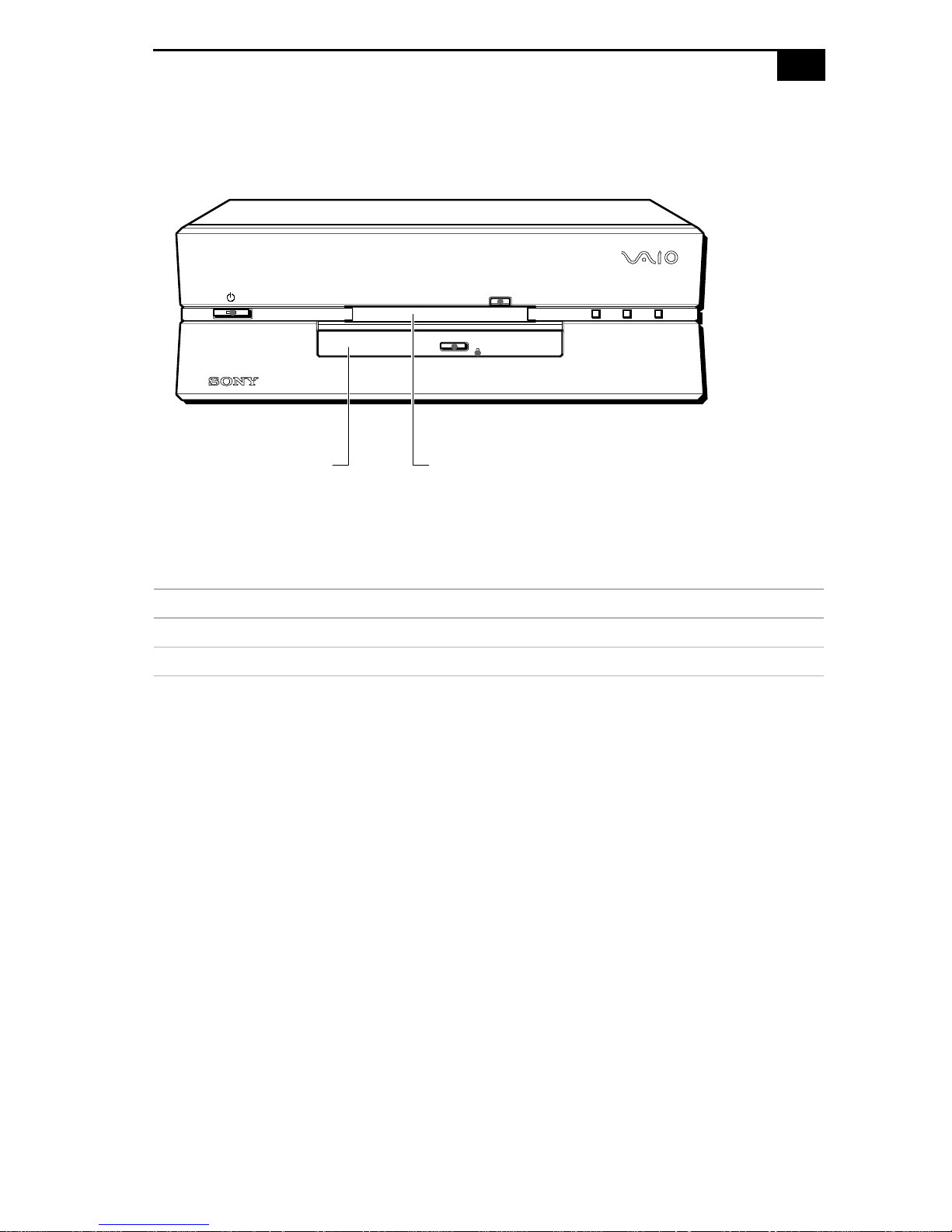
Front View
Flip-down panel
FD CD HD
SHA0001.VS
Page 11
Identifying Components
Drives
3
FD CD HD
Floppy disk driveCD-ROM disc drive
SHA0002.VSD
Drive Description
Diskette drive 3.5-inch, 1.44 Mbyte.
CD-ROM drive CD-ROM disc read: 24X (maximum performance).
* Data on a CD-ROM disc is read at a variable transfer rate, ranging from 10.3X at the innermost track to
24X at the outermost track (the data transfer standard 1X r ate is 150 kbytes/s). T he average data tr ansfer
rate is 17X (2550 kbytes/s).
*
Page 12
4
VAIO Computer Reference Manual
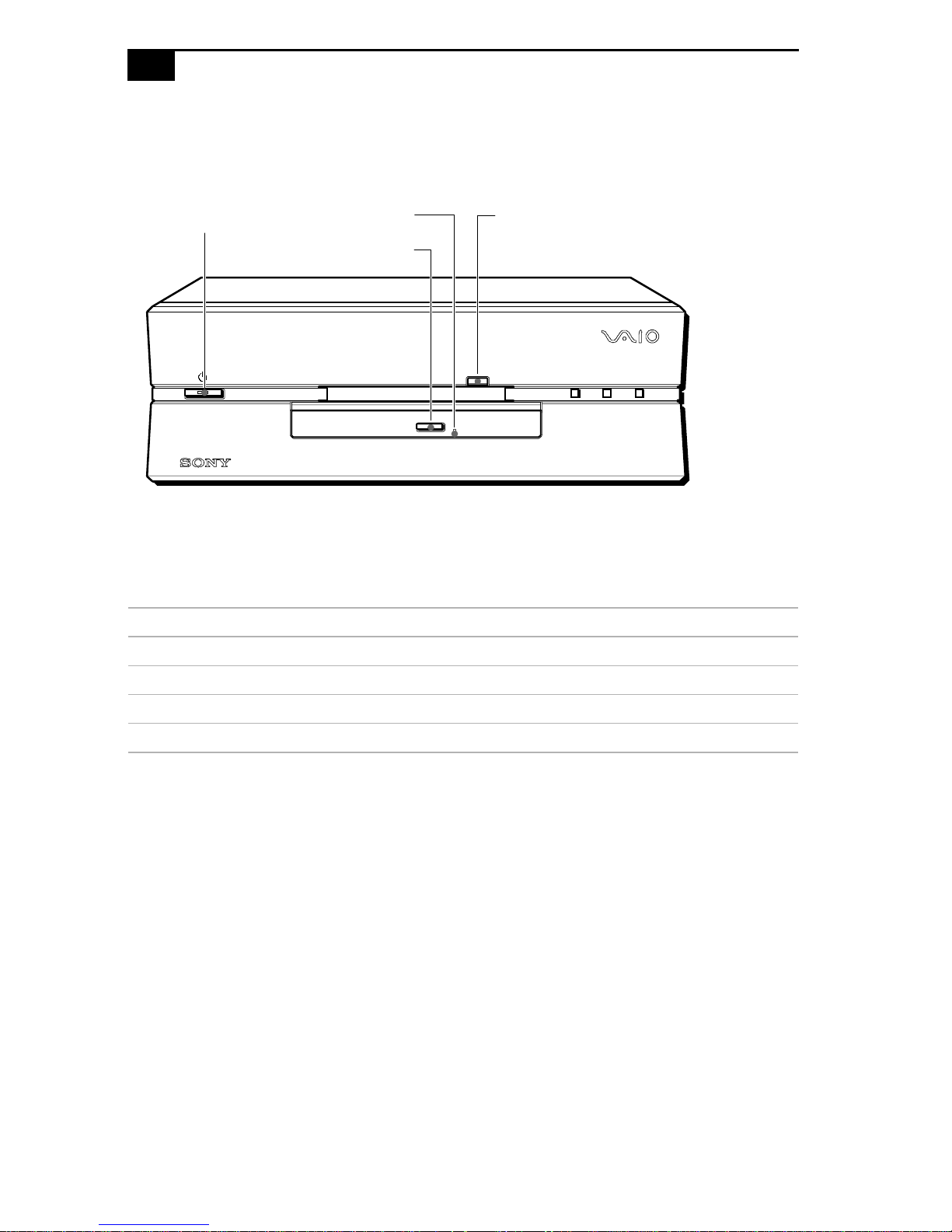
Buttons and Switches
Power on/off Floppy disk eject
Manual eject hole
CD-ROM disc eject
FD CD HD
Button or switch Description
Power/Standby switch Turns system power on and off.
SHA0003.VSD
Floppy disk eject button Ejects a diske tte.
CD-ROM disc eject button
Automatically opens and closes the CD-ROM tray.
Emergency eject hole Ejects a CD-ROM disc.
Page 13

Identifying Components
Indicators
Power on/off
5
FD CD HD
Diskette drive access indicator
CD-ROM drive access indicator
Hard drive access indicator
SHA0004.VSD
Indicator Description
Power/Standby indicator Sta ndby (amber ) indicates th e computer is in
standby mode. On (green) indicates the
computer is out of standby mode, ready to
use. Off (no color) indicates the computer is
turned off.
Diskette drive access indicator On (green) indicates diskette drive activity.
CD-ROM drive access
On (orange) indicates CD-ROM disc activity.
indicator
Hard disk drive access
indicator
On (orange) indicates hard disk drive
activity.
Page 14
6
D
VAIO Computer Reference Manual
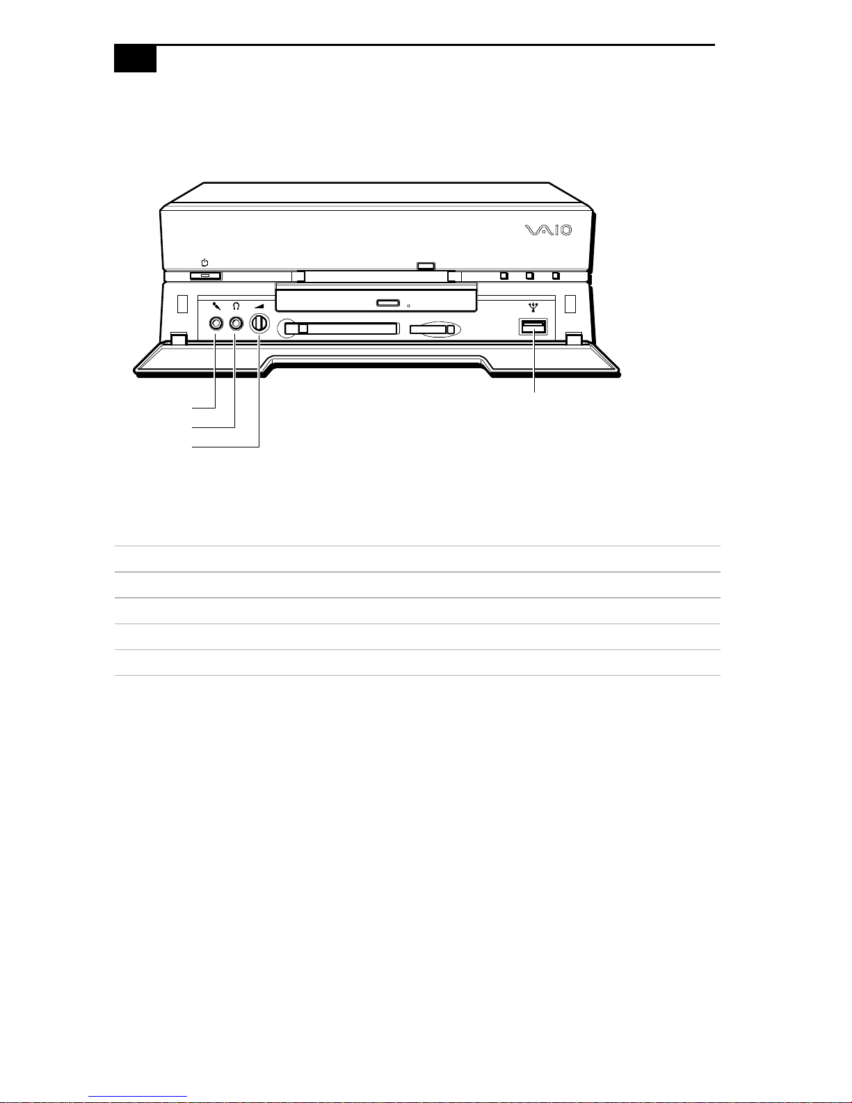
Connectors
MIC
PHONES
VOLUME
Connector Description
MIC Connects to microphone.
PHONES Connects to headphones.
USB Connects to USB devices.
VOLUME Controls volume.
FDCDH
USB
D
SHA0005.VS
Page 15
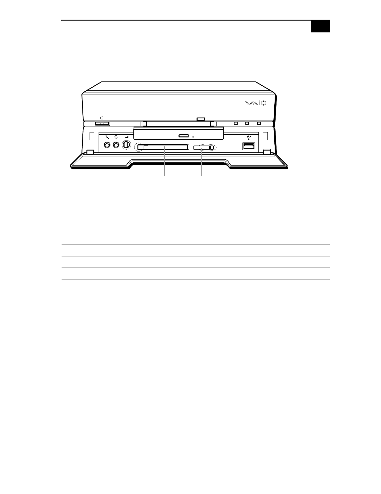
Slots
D
Identifying Components
7
FDCDH
PC Card Slot Memory Stick
Media Slot
D
Slot Description
PC Card Slot Accommodates one Type II PCMCIA card
™
Memory Stick
Media Slot Accommodates Memory Stick media
SHA0006.VS
Page 16

8
VAIO Computer Reference Manual
Rear View
Power LINE PHONE
PRINTER SERIAL MONITOR
PRINTER SERIAL MONITOR
USB
USB LINE VIDEO
OUTIN
OUT
LINE OUT
LINE IN
LIN
E
LCD KEYBOARD
LCD*
PHON
E
KEYBOARD
Connector Description
Power AC input power
LINE Connects to phone cable from wall jack
PHONE Connects to telephone
PRINTER Connects to parallel device
SHA0007.VSD
SERIAL Connects to serial device
MONITOR Connects to VGA monitor
USB Connects to USB devices
LINE IN Connects to output connector on audio device
LINE OUT Connects to input connector on audio device
LCD Connects to VAIO Slimtop LCD
KEYBOARD Connects to keyboard
* VAIO Slimtop LCD models only.
*
monitor
Page 17
Identifying Components
9
I/O Connectors
The following section identifies the various I/O connectors.
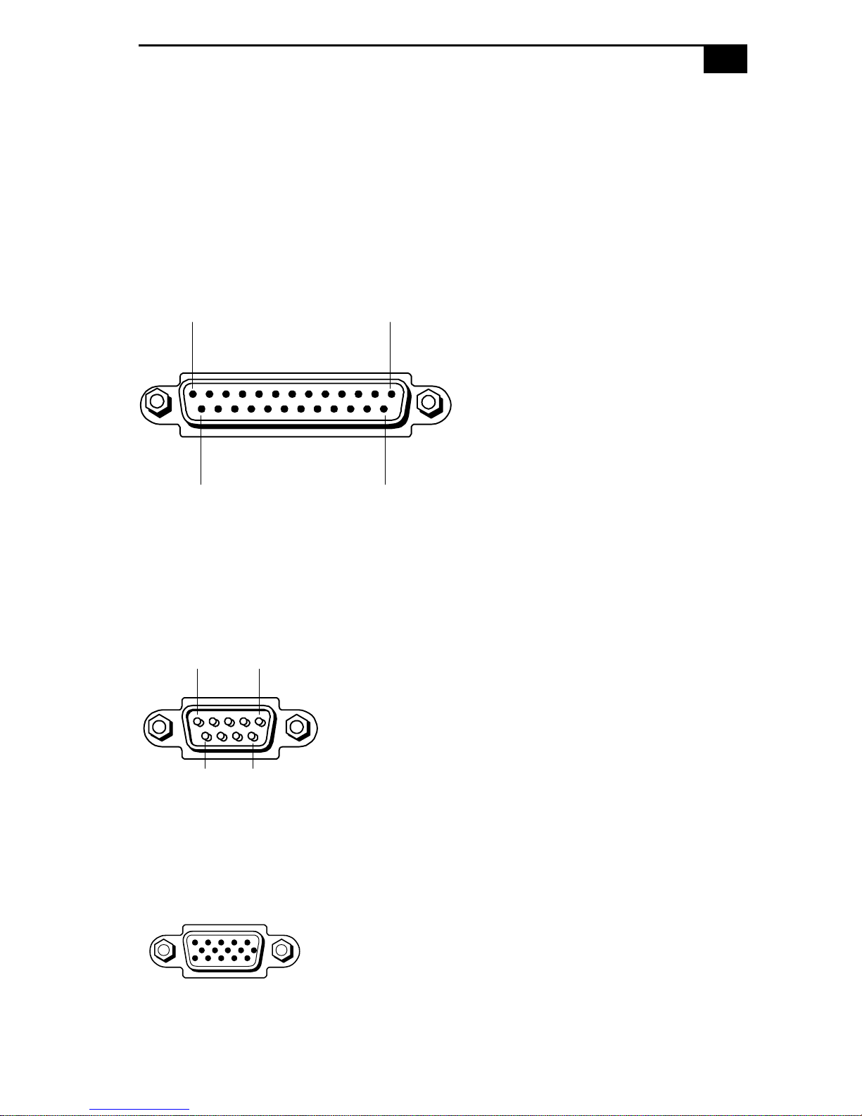
PRINTER Port
The PRINTER port is a standard 25-pin DB-25 female connector assigned
as LPT1.
13 1
25 14
KY0005.VSD
SERIAL Port
The SERIAL port is a standard 9-pin DB-9 male connector assigned as
COM1.
51
9
6
KY0057.VSD
MONITOR
The MONITOR connector is a standard 15-pin female high-density VGAtype connector.
SHA0009.VSD
Page 18
10
D
VAIO Computer Reference Manual
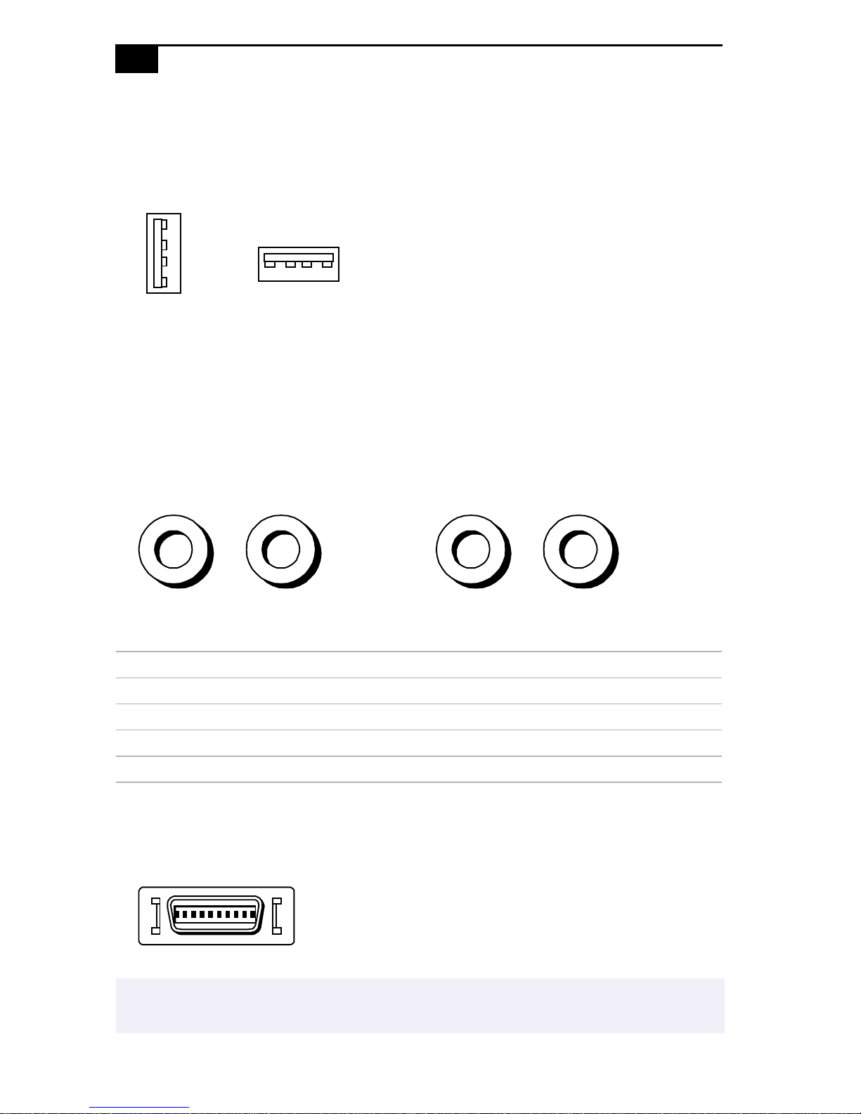
USB Ports
A USB port is located on the front and real panels.
Rear panel
Front panel
KY0003.VS
PHONE, MIC, LINE IN, and LINE OUT
The PHONES, MIC, LINE IN, and LINE OUT jacks are physically
identical, but have differ ent connections. They are standar d 3.5 mm ster eo
mini-jacks. The PHONES and MIC jacks are located on the front panel.
The LINE IN and LINE OUT jacks are located on the rear panel.
PHONES MIC
Front panel
LINE IN LINE OUT
Rear panel
Connector Description
PHONES 1.0 Vrms output (typical)
MIC Electrolet condenser microphone input
LINE IN 1.0 Vrms input (typical), 10 Kohm impedance
LINE OUT 2.0 V rms out (max)
LCD (VAIO Slimtop LCD models only)
The LCD connector is a 26-pin female MDR-type connector.
KY0013.VSD
! Do not connect any other LCD monitor other than the Sony VAIO Slimtop LCD
monitor.
KY0004.VSD
Page 19

Identifying Components
KEYBOARD
The KEYBOARD connector is a standard 6-pin PS/2®-type female
connector.
2
11
3
4
5
1
6
KY0002.VSD
LINE and PHONE
The LINE and PHONE jacks are physically identical and have identical
connections. They are standard RJ-11 female phone jacks. However, the
LINE jack is for connecting to a telephone line that comes from the wall
jack, and the PHONE jack is for connecting the computer to a telephone.
LINE PHONE
KY0014.VSD
✍ Accidentally plugging a phone line from the wall into the modem’s PHONE jack, and a
telephone into the LINE jack, will not damage the modem card or telephone equipment.
However, the modem will not work correctly.
Page 20
12
VAIO Computer Reference Manual
Expansion Slot
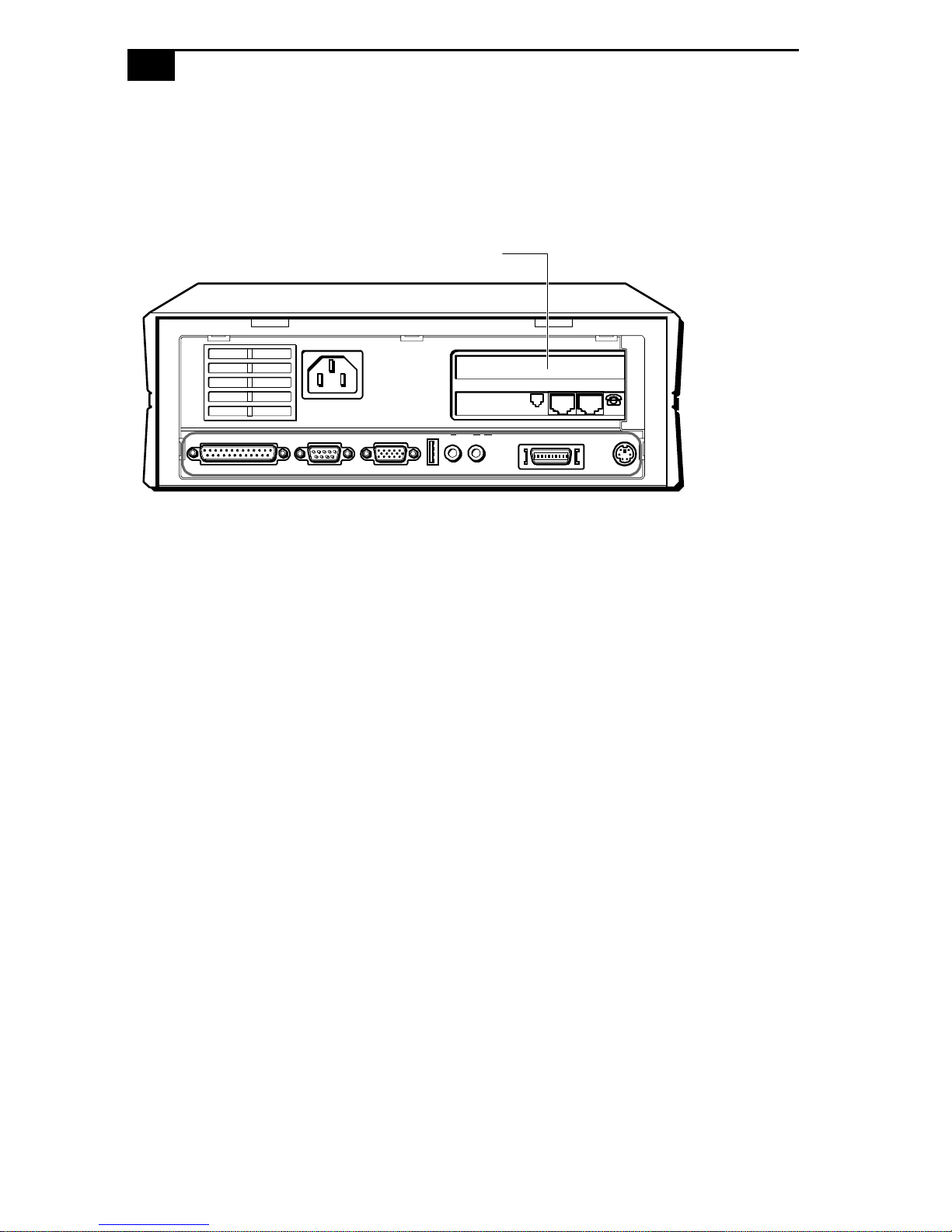
One PCI slot is available for expansio n. The other PCI slot is occupied by
the fax/modem card.
PCI Slot
LINE PHONE
PRINTER SERIAL MONITOR
USB LINE VIDEO
OUT
OUTIN
LCD KEYBOARD
SHA0008.VSD
Page 21

Chapter 2
Configuring Your System
This chapter contains information on configuring your system.
Configuring your system can consist of the followin g:
❑ Making changes to the CMOS settings
❑ Making changes to the disp lay's power management s et tings
❑ Changing the system board jumper position
13
Page 22

14
VAIO Computer Reference Manual
Accessing the CMOS Setup Utility
You mu st access the CMOS Setup Utility to ma ke changes to the CMOS
settings (see “CMOS Setup Options” on page 65 for information on
CMOS settings).
! Before rebooting the system, save any open files and exit Windows
®
.
1 Reboot the system. The follow ing message appears during the in itial
boot sequence:
Press TAB to show POST screen, DEL to enter SETUP
2 Press DEL after the progress bar starts.
3 Use the arrow keys to select an item from the main menu.
4 Press Enter to display the options for the selected item.
5 Use the arrow keys to select an option.
6 Press Page Up or Page Down to modify the setting.
7 Press ESC to return to the main menu.
8 Select SAVE & EXIT SETUP, then press Enter. Follow the onscreen
prompts.
Page 23
Configuring Your System
15
Changing the Display's Power Management
Settings
A display that has power management capability is designed to operate
on reduced power or shut itself off after the system has been idle for a
specified period of time.
1 From the Start menu, point to Settings, then click Cont rol Panel.
2 Click the Display icon.
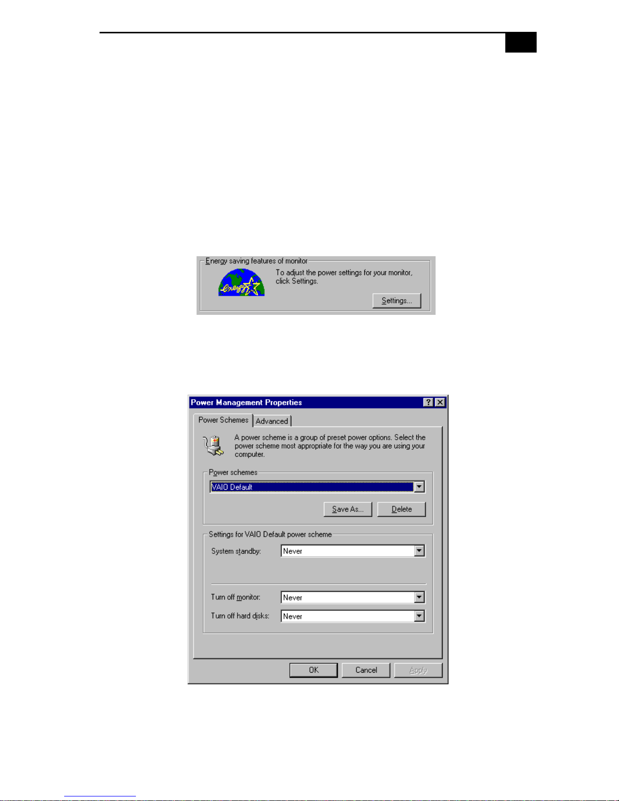
3 Click the Screen Saver tab. The Energy-Star dialog box opens.
4 Click Settings.
The Power Management Properties dialog box opens, with the Pow er
Schemes tab displayed.
5 Select the power scheme that is most appropria te for the way you use
your computer.
To change a power scheme, change the settings for System standby,
Page 24
16
VAIO Computer Reference Manual
Turn off monitor, and Turn off hard disks.
The System standby option allows you to specify the period of
inactivity (in minutes) that y ou want to elapse before your computer
goes on standby when your computer is running on AC power.
Power is reactivated when you move the mouse or press a key.
The Turn off monitor option allows you to specify the period of
inactivity (in minutes) that y ou want to elapse before your monitor
turns off when your computer is running on AC power. The display
reactivates when you move the mouse or press a key.
The Turn off hard disks option allows you to specify the period of
inactivity (in minutes) that you want to elapse before your hard disks
turn off when your computer is running on AC power.
6 To save a new power scheme, first modify the settings, click Save As,
type a descriptive name, and then click
OK.
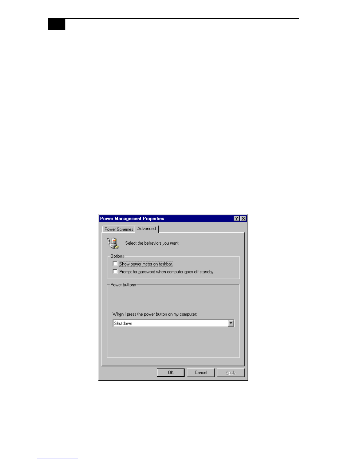
7 Click the Advanced tab.
8 Select the desired settings, and then click OK.
Page 25

Configuring Your System
Configuring the System Board
The system board contains the following configuration jumpers:
❑ Clear CMOS
❑ VGA Enable
❑ INTEN
The configuration jumpers should never need changing unless otherwise directed by a
✍
technical support or service technician.
! Before opening the system, save any open files, exit Windows, turn off the
power of the computer and all attached peripherals, and unplug the
power cord.
Clear CMOS Jumper
17
The Clear CMOS jumper provides two modes of operation: Normal
mode, and Clear CMOS mode.
Normal mode allows normal access to the BIOS Setup Utility. The Central
Processing Unit (CPU) input clock is forced to remain at 100 MHz (fast
mode), and the Basic Input/Output System (BIOS) uses the User CMOS
settings (as opposed to the System CMOS settings). The CMOS and
NVRAM settings are only cleared if the checksum test returns false.
Access to specific setup fields is controlled by a supervisor password or
user password.
The Clear CMOS mode removes the pa ssword that is stor ed in CMOS. No
other parameters are cleared.
To change the Clear CMOS jumper, perform the following steps:
1 Remove the system cover (see “Removing the System Cover” on
page 20).
2 Set the jumpers as directed by a service technician (also see “CMOS
Clear (CMOS)” on page 59).
3 Reinstall the system cover (see “Replacing the System Cover” on
page 21).
VGA Enable Jumper
You can enable or disable the onboard VGA controller if you install a
VGA PCI add-in card.
Page 26

18
To change the VGA enable jumper, perform the following steps:
VAIO Computer Reference Manual
1 Remove the system cover (see “Removing the System Cover” on
page 20).
2 Set the jumper to enable or disable (see “VGA Enable (VGAEN)” on
page 60).
3 Reinstall the system cover (see “Replacing the System Cover” on
page 21).
INTEN Jumper
You can enable or disable the onboard VGA interrupt if you install a VGA
PCI add-in card.
To change the INTEN jumper, perform the following steps:
1 Remove the system cover (see “Removing the System Cover” on
page 20).
2 Set the jumper to enable or disable (see “INTEN” on page 61).
3 Reinstall the system cover (see “Replacing the System Cover” on
page 21).
Page 27

Chapter 3
Removing, Installing, and
Replacing Components
This chapter describes removing, installing, and replacing major
components for upgrading, reconfiguring, and troubleshooting the
components.
! Before opening the system unit, save any open files, exit Windows, turn off
the power of the computer and all attached peripherals, and then unplug the
power cord.
19
Page 28

20
VAIO Computer Reference Manual
Removing the System Cover
You must remove the system cover to access the system board, add-in
cards, power supply, battery, and internal drives.
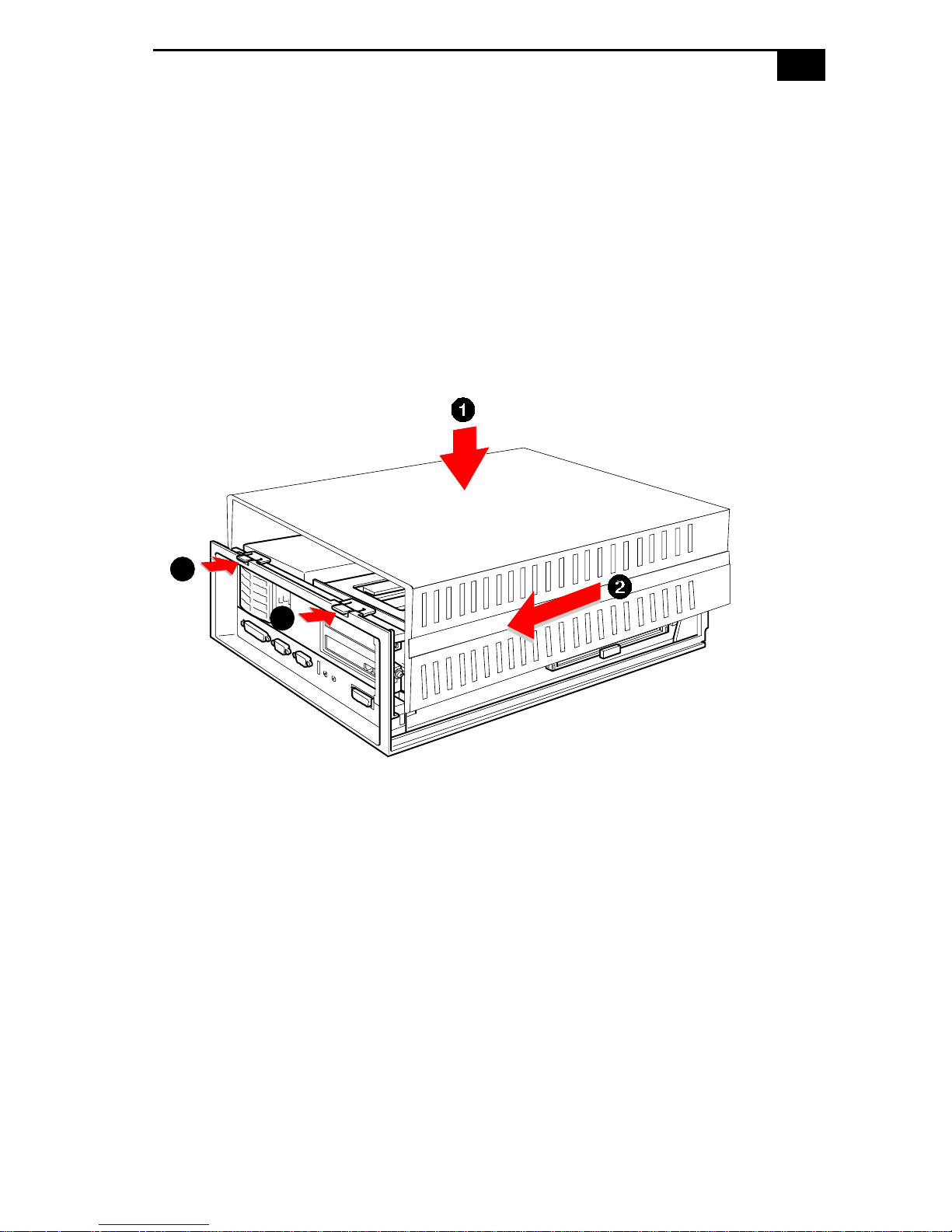
1 From the rear of the unit, push down on the two tabs that secure the
system cover to the chassis.
2 Slide the system cover back. The panel slides back about ½ inch.
3
✍
This works best if the spacers are installed on the unit, or the unit sits on a rubber mat.
3 Lift straight up to remove it.
KY0064B.VSD
Page 29
Removing, Installing, and Replacing Components
21
Replacing the System Cover
1 Position the system cover over the chassis such that the front portion
of the system cover extends past the front of the unit.
2 Carefully lower the system cover down over the chassis. The rear of
the system cover should be about ½ inch in from the rear of the unit.
3 Carefully slide the system cover back until the tabs snap into place.
Check the front to make sure all drives and connectors are correctly
aligned.
3
3
KY0077.VSD
Page 30
22
VAIO Computer Reference Manual
Installing an Add-In Card
! Before opening the system unit, save any open files, exit Windows, turn off
the power of the computer and all attached peripherals, and then unplug the
power cord.
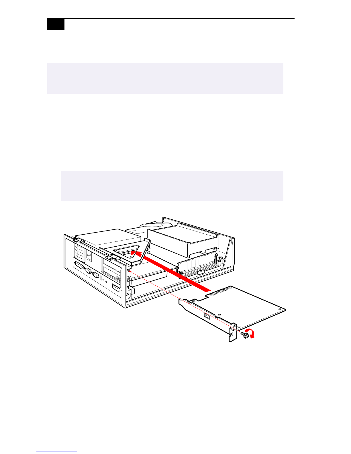
1 Remove the system cover (see “Removing the System Cover” on
page 20).
2 Remove the slot cover adjacent to the selected slot connector on the
system board (see “Removing a Slot Cover” on page 32).
3 Insert the add-in card into the PCI slot connector. Use a gentle
rocking motion, pressing down until the card is fully seated.
✍
Align the card's bracket so that the bottom of the bracket fits into the slot at the
bottom of the chassis. Assure that the top of the bracket fits snugly against the
chassis lip after the card is fully inserted.
4 Attach any necessary cables to the car d (see the instructions that came
with the add-in card).
5 Replace the system cover (see “Replacing the System Cover” on
page 21).
6 Turn on the computer and follow any instructions that came with the
add-in card.
KY0070.VSD
Page 31
Removing, Installing, and Replacing Components
Removing an Add-in Card
! Before opening the system unit, save any open files, exit Windows, turn off
the power of the computer and all attached peripherals, and then unplug the
power cord.
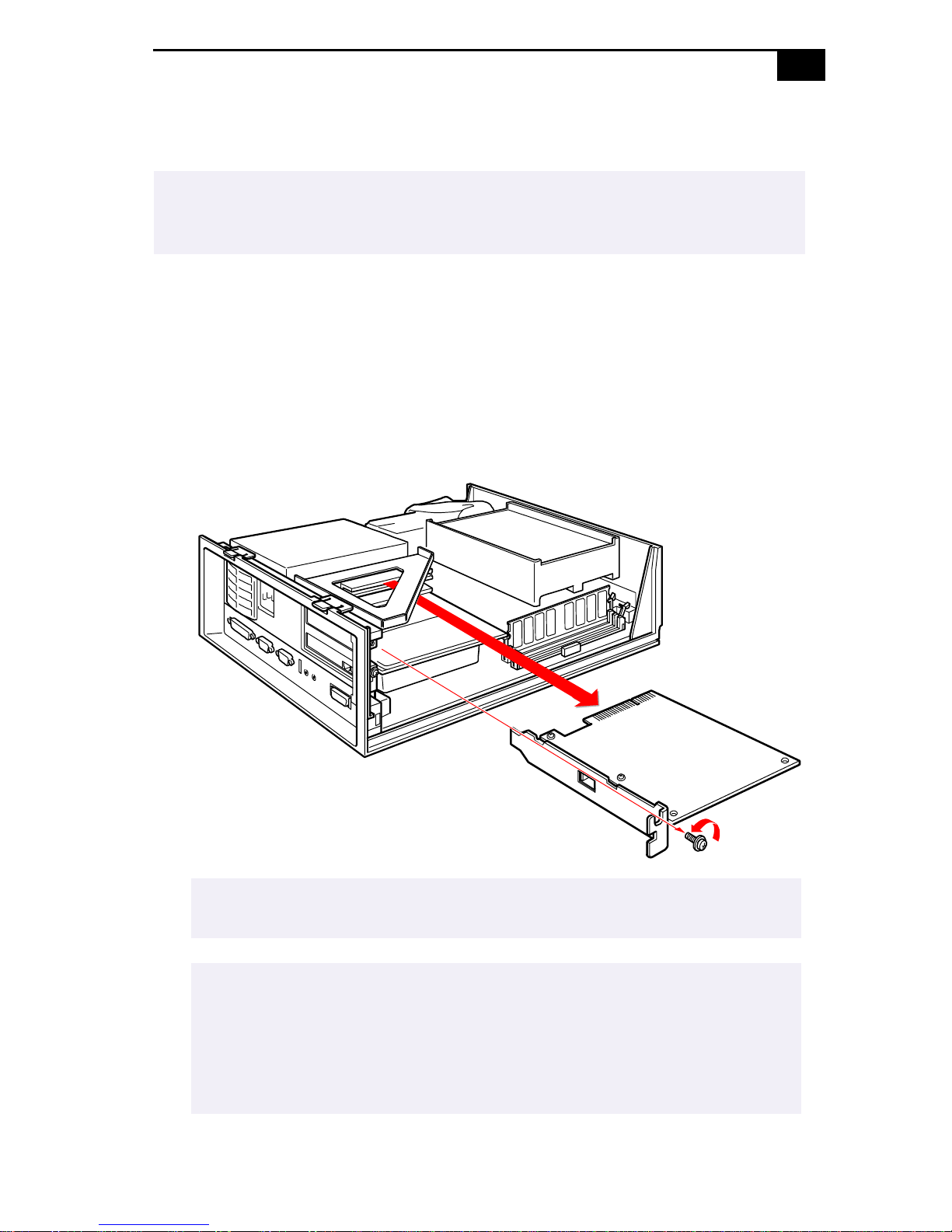
1 Remove the system cover (see “Removing the System Cover” on
page 20).
2 Disconnect any cables attached to the add-in card.
3 Remove the screw that secures the add-in card to the chassis.
4 Remove the add-in card from the PCI slot connector and store the
card in an anti-static wrapper for future use.
23
✍
Grasp the card with one hand on each end, and gently pull up as you rock the card
from side to side.
! Hold the add-in card by its edges and do not touch any components or
connector contacts on the card. Static electricity in your body may
damage sensitive components on the card. As a precaution, touch any
exposed metal part on the metal chassis (preferably the metal part on
the power supply) before handling an add-in card to discharge any static
electricity in your body.
KY0071.VSD
Page 32

24
VAIO Computer Reference Manual
5 If you do not replace the card or install another add-in card, install a
slot cover over the vacant slot at the rear of the chassis (see “Covering
an Open I/O Slot” on page 33).
6 Replace the system cover (see “Replacing the System Cover” on
page 21).
Page 33

Removing, Installing, and Replacing Components
25
Replacing the Lithium Battery
You may need to replace the lithium battery if your computer consistently
loses the date or time settings after turning it off. The lithium battery has
a typical life of three years, after which the battery may be too weak to
power the CMOS memory.
! When you remove the lithium battery, all values stored in the CMOS memory
(BIOS setup values and Plug and Play values) may be lost. Although the
computer can hold the charge for a short time while replacing the battery, it
is safer to as sume that the setti ngs w ill be l ost. W h en the va lues are l ost , the
BIOS values revert to their factory-default settings (see “Accessing the
CMOS Setup Utility” on page 14).
Do not handle damaged or leaking batteries.
The lithium battery may explode if mistreated. Do not disassemble it or
dispose of it in fire.
1 Reboot your computer by selecting Shut Down... from the Start
menu, and then selecting Restart the computer.
2 If the error message “Error: Check date and time settings” appears
during the reboot sequence, pr ess F3, then press F2 during the reboot
process to access the BIOS Setup Utility. Otherwise it is not necessary
to replace the battery at this time, and you can skip all remaining
steps.
3 Compare all the BIOS options to their default settings (see “CMOS
Setup Options” on page 65). Make a list of all the BIOS options that
are different from their default values. You will refer to this list when
you restore the BIOS settings later.
4 Press ESC, then select Exit from the main menu using the right arrow
key. The Exit Discarding Changes is automa tically selected (it is the
first item in the list).
5 Press Enter, type N when prompted to save, then press Enter to exit
the BIOS Setup Utility.
6 Turn off the computer and unplug the power cord.
7 Remove the system cover (see “Removing the System Cover” on
page 20).
Page 34
26
VAIO Computer Reference Manual
8 Remove all add-in cards (see “Removing an Add-in Card” on
page 23) to gain access to the battery. You may also need to
disconnect some cables.
! Touch any exposed metal part of chassis to discharge static electricity in
your body before handling an add-in card or other sensitive electronic
component.
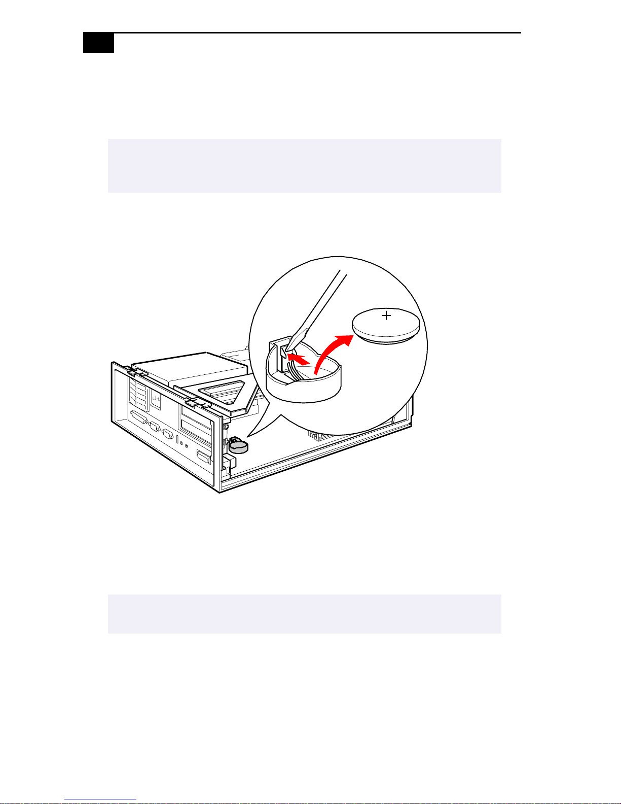
9 Insert a small flathead screwdriver into the small space at the top of
the battery holder.
KY0072.VSD
10 Gently pry the battery out and dispose of it according to the
instructions that came with the new battery.
11 Insert the new battery into the battery holder, wi th the plus (+) side
up.
✍
The Sony CR2032 battery is recommended. Using a type of battery other than a
CR2032 may present a risk of fire or explosion.
12 Replace all add-in cards that were removed.
13 Reconnect any cables that were disconnected.
14 Replace the system cover (see “Replacing the System Cover” on
page 21).
15 Reconnect the power cord and turn on the computer.
Page 35

Removing, Installing, and Replacing Components
27
16 If the error message “Error: Check date and time settings.” appears
during the reboot sequence, press DEL to access the CMOS Setup
Utility. If no error message displays, the computer’s CMOS settings
were retained during the battery replacement and you can skip the
remaining steps.
17 Refer to the list you made in step 3 and restore any non-default
CMOS settings (see “CMOS Setup Options” on page 65).
18 Select SAVE & EXIT SETUP from the main menu using the arrow
keys, then press Enter.
19 Type Y, then press Enter to save the changes and exit the CMOS Setup
Utility.
The computer’s CMOS settings are now restored.
Page 36

28
VAIO Computer Reference Manual
Installing System Memory
! Before opening the system unit, save any open files, exit Windows, turn off
the power of the computer and all attached peripherals, and then unplug the
power cord.
1 If necessary, remove the memory module you wish to replace (see
“Removing a Memory Module” on page 30).
2 Remove the new memory module(s) from its anti-static package.
Hold the memory module only by its edges to prevent staticelectricity damage.
3 Choose the size of the memory module and configuration as shown
in the following table. Memory modules can vary in size and speed
between sockets. The minimum memory size is 8 MB. The maximum
memory size is 256 MB. The BIOS automatically detec ts the type, size,
and speed of the memory modules.
Memory module configurations (MB)
*
DIMM1 DIMM2
0, 8, 16, 32, 64, 128 0, 8, 16, 32, 64, 128
* The PCV-L400 is shipped with 64 MB. The PCV-L600 and
PCV-L600S are shipped with 128 MB. SDRAM is expandable to
256 MB on all models.
! Touch any exposed metal part of the chassis to discharge static electricity in
your body before handling a memory module.
✍
Use only 100 MHz FSB-supported memory. Do not mix 66 MHz memory with 100 MHz
memory. Supports SDRAM memory. Does not support EDO memory or buffered DIMM
memory.
Page 37
Removing, Installing, and Replacing Components
29
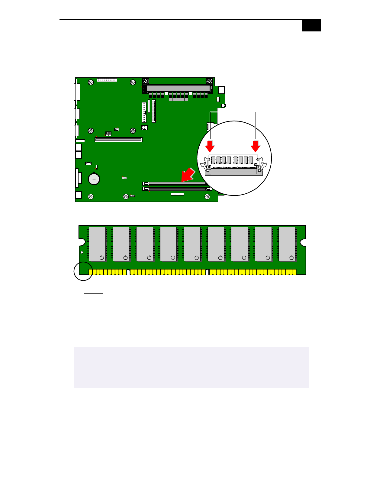
4 Align the module over the appropriate socket, noting the location o f
pin 1 on the module and pin 1 on the socket.
Press down
here
Pin 1 side
DIMM2
DIMM1
Memory module (DIMM)
1
Indicates pin 1
Handles
OM04586.VSD
5 Carefully but firmly insert the edge of the module into the socket.
6 Press down firmly and evenly at both corners until the module is
fully seated.
✍
When the module is fully seated, the handles on each side are straight up and
locked into the slot on each side of the module. If the handles are not totally
straight upright, continue to press down on each side of the module until the
handles lock into place.
7 Replace the system cover (see “Replacing the System Cover” on
page 21).
Your computer automatically recognizes the extra memory and
configures itself accordingly when you turn it on. No further action is
required.
Page 38
30
VAIO Computer Reference Manual
Removing a Memory Module
You may need to remove a memory module if you change the memory
configuration or replace a bad module.
! Before opening the system unit, save any open files, exit Windows, turn off
the power of the computer and all attached peripherals, and then unplug the
power cord.
1 Remove the system cover (see “Removing the System Cover” on
page 20).
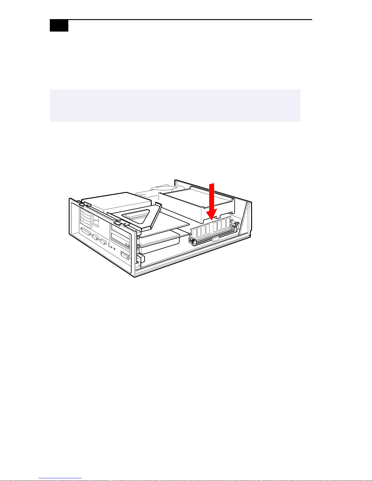
2 Locate the memory module you wish to remove.
KY0073.VSD
Page 39
Removing, Installing, and Replacing Components
31
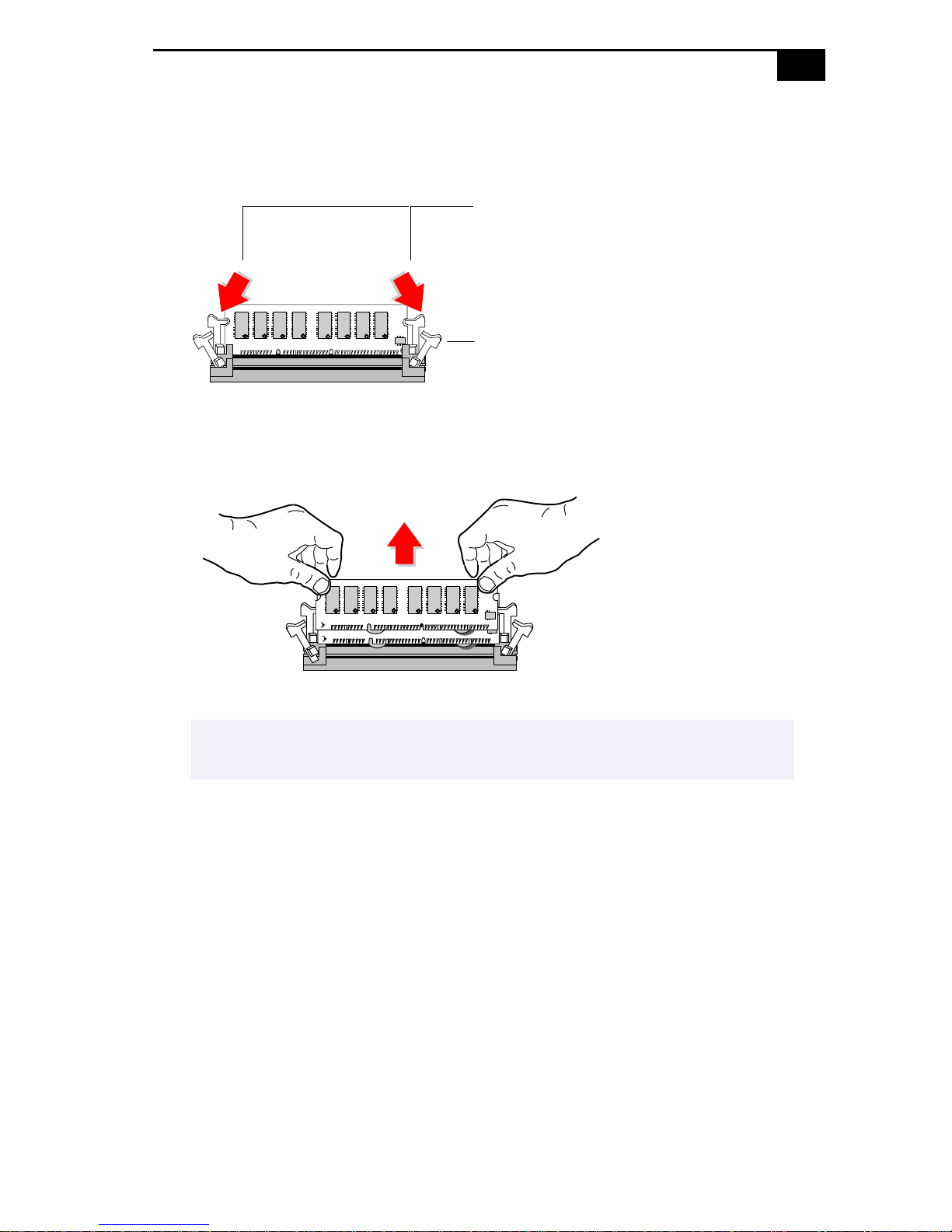
3 Push out the handle on each side of the memory module to eject the
module from its socket.
Push out
Handles
KY0042.VSD
4 Lift the memory module out by grasping it by its edges. Store the
module in a static-free bag.
! Touch any exposed metal part of the chassis to discharge static
electricity in your body before handli ng the memory module.
KY0043.VSD
Page 40
32
VAIO Computer Reference Manual
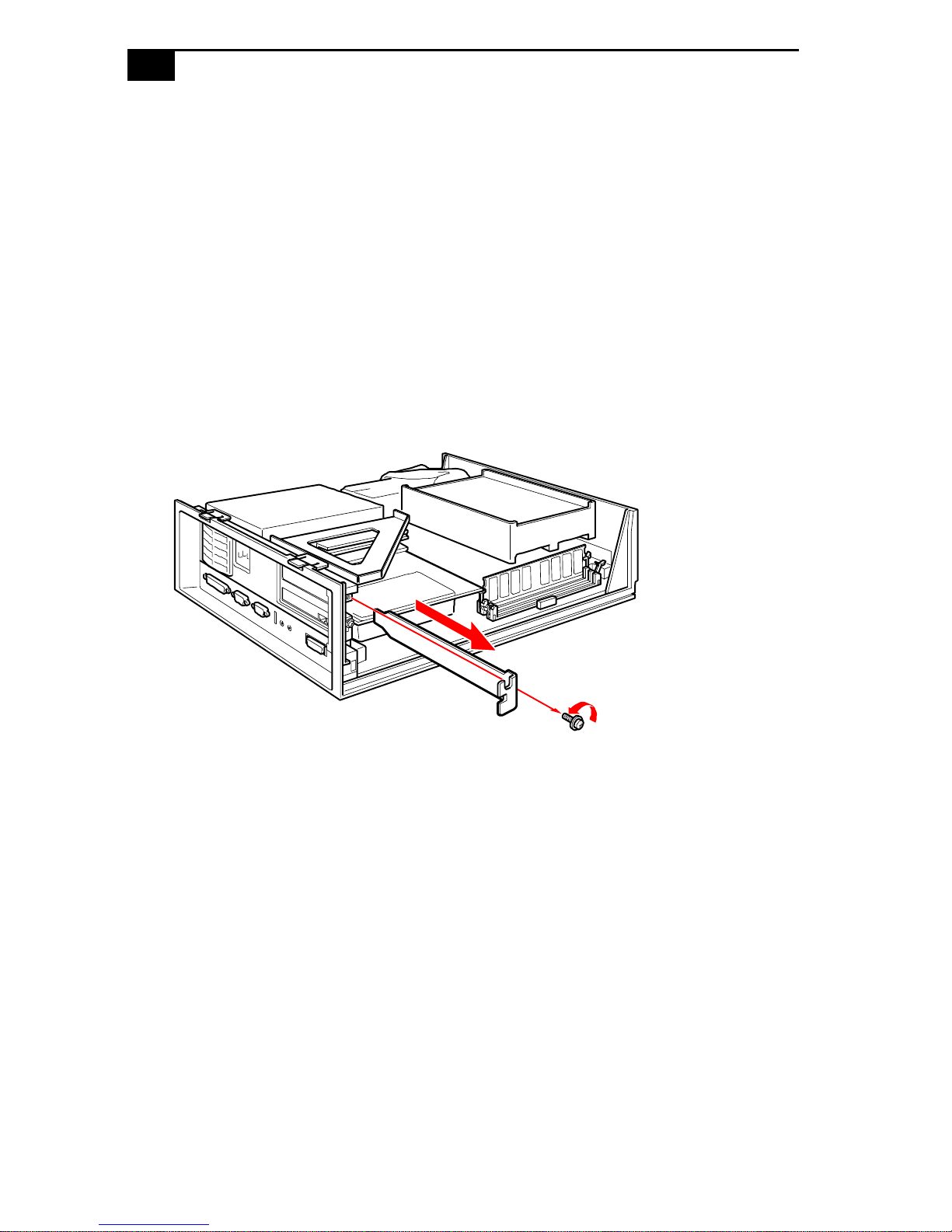
Removing a Slot Cover
You remove a slot cover when you install an add-in card that occupies a
previously-empty slot.
1 Lay the system on its side with the open side facing up and the slot
covers facing you.
2 Locate the slot of the cover you want to remove.
3 Remove the screw from the slot cover.
4 Carefully remove the loose slot cover and retain it for future use.
KY0069.VSD
Page 41
Removing, Installing, and Replacing Components
33
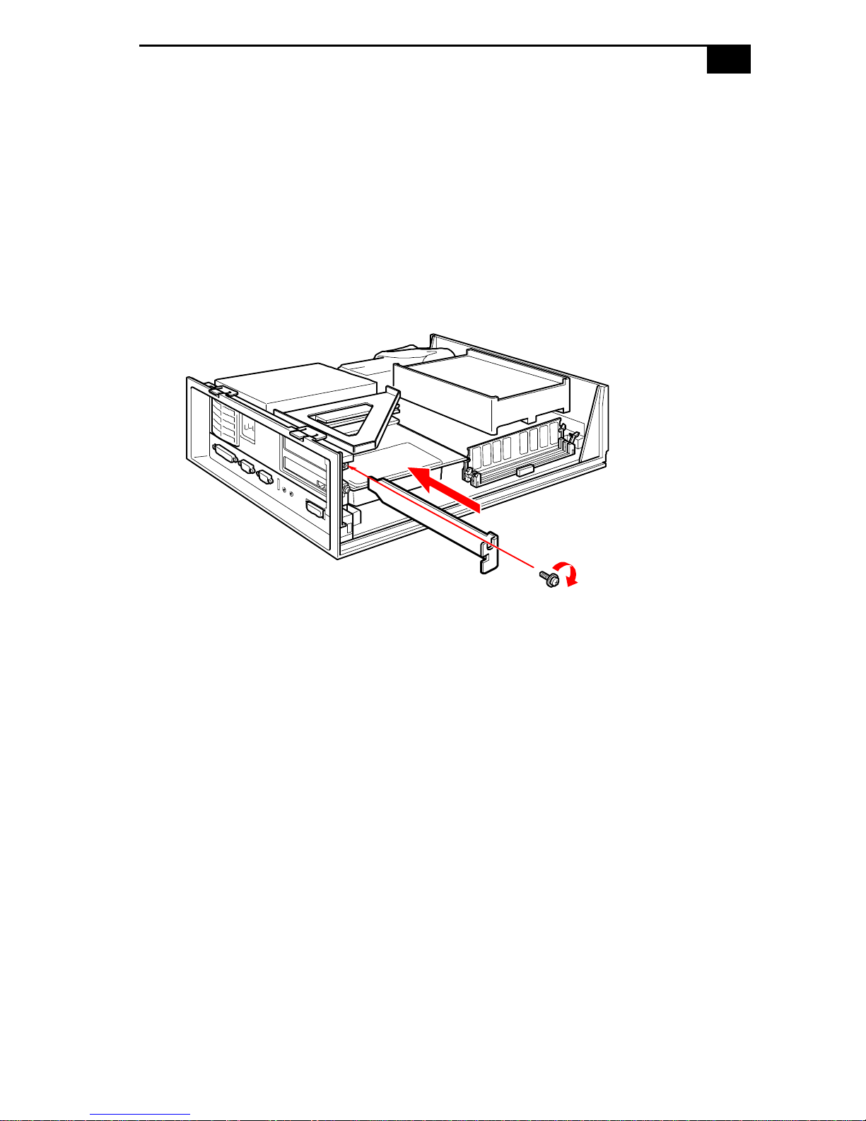
Covering an Open I/O Slot
Slot covers prevent air from escaping through the empty hole. If air
escapes, the components inside the computer cannot be properly cooled.
This may damage some components, especially the main processor
(which generates the most hea t) .
1 Fit the bottom end of the slot cover (removed earlier) between the
chassis and system board.
KY0076.VSD
2 Push the slot cover in until it rests firmly on the lip in the chassis. All
add-in card brackets and slot covers rest on this lip.
3 Replace the screw (removed earlier) to secure the I/O slot cover.
Page 42

34
Page 43
Chapter 4
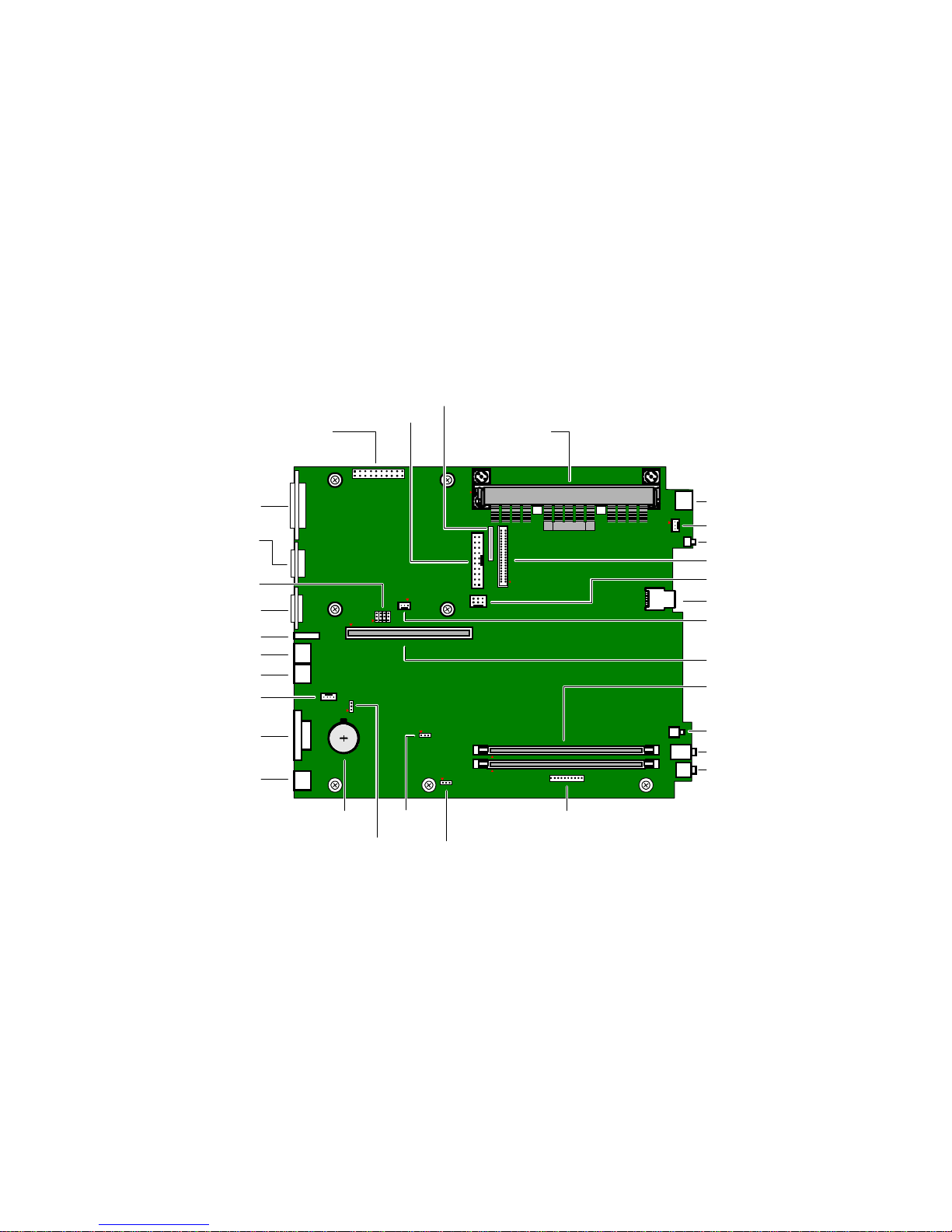
System Board
This chapter identifies each component on the system board and provides
a detailed description of each connector and ju mper on the system board.
Floppy
Power
Primary IDE CPU
Printer
Serial
CPU Bus Freq.
Multiplier
VGA Monitor
USB1
Line In
Line Out
AUX
LCD Monitor
Keyboard/Mouse
Battery
CMOS
Clear
VGAEN
INTEN
USB2
CPU Fan
Reset
Secondary IDE
PS Fan
Sony Memory Stick
Wake On LAN
PCI Riser Slot
Memory
Volume
Phone
Mic
Front Panel
OM04581.VSD
35
Page 44
36
D
VAIO Computer Reference Manual
Connectors
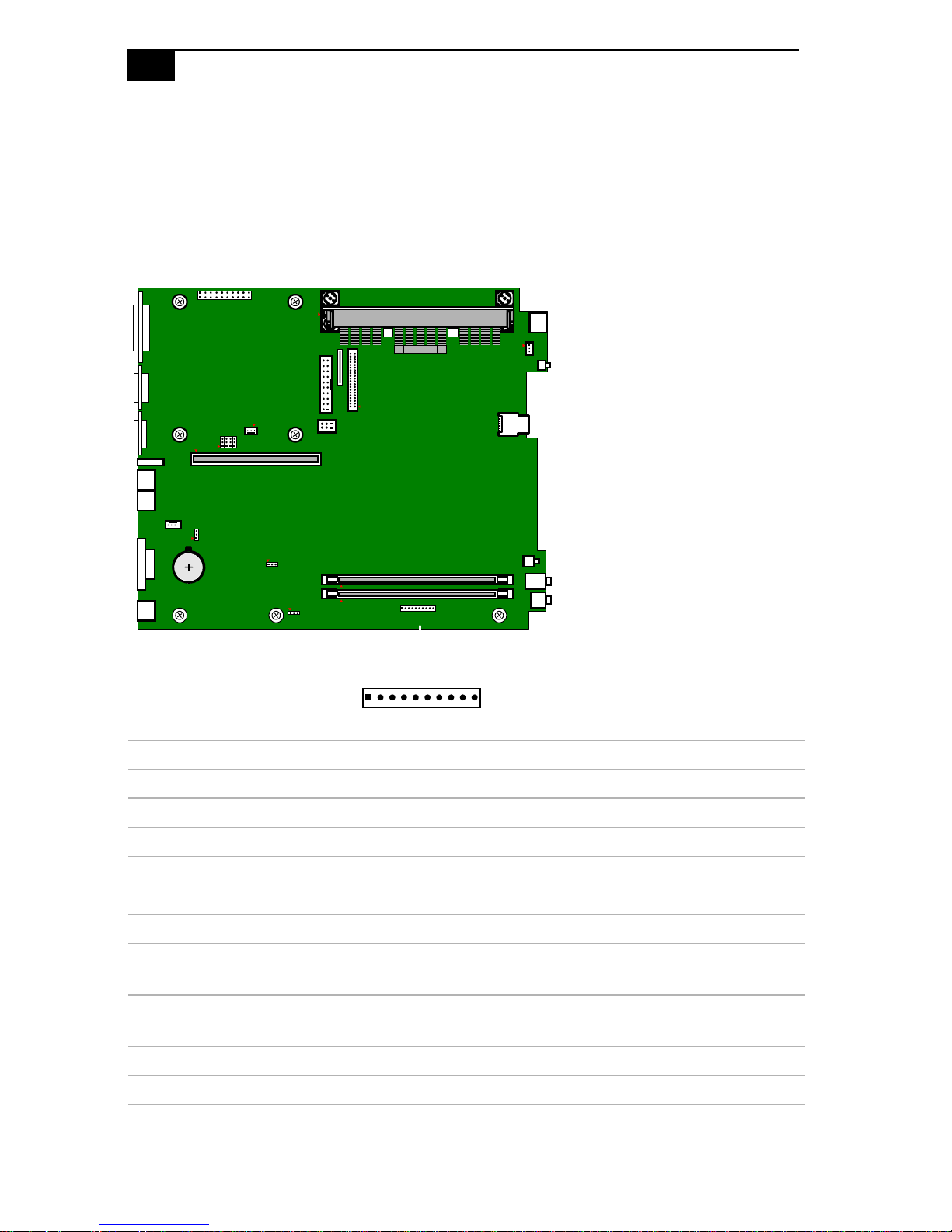
Front Panel Header
The front panel header is a 10-pin header that provide connections to
various front panel functions.
Front panel header
Pin # Name Description
1 +5 +5V from power supply
2 LED (CD-ROM) Connects to LED on CD-ROM
3 LED (FDD) Connects to LED on floppy disk drive
4 LED (HDD) Connects to LED on IDE hard disk drive
5 LED (MODEM) Connects to LED on modem card
6 Reserved (not used)
7 LED3 Connects to Standby/Sleep (red) signal from
power supply
8 LED4 Connects to Power (green) anode signal from
power supply
9 POWER SW Connects to power switch
10 GND Connects to signal ground
KY0031.VS
Page 45
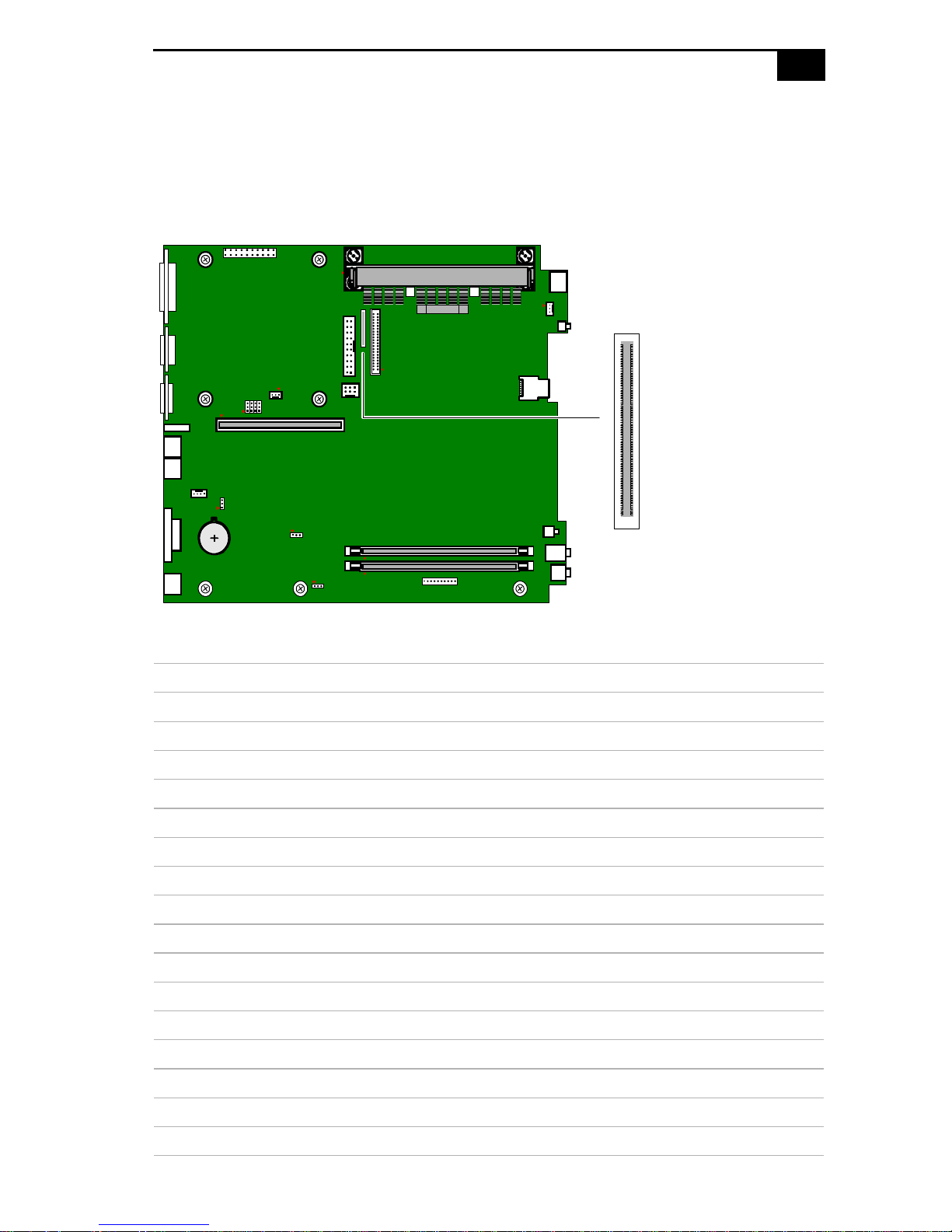
System Board
Diskette Drive (FLOPPY) Connector
The FLOPPY connector is a 26-pin connector for a slim notebook-type
diskette drive.
FLOPPY
37
Diskette Drive connector
Pin Signal
1+5V
2INDEX
3+5V
4 DRIVE_SELECT_0#
5+5V
6DSKCHG#
7NC
8READY#
9HD
10 MOTOR_ON#
11 NC
12 DIRECTION#
OM04701H.VSD
13 MODE_SELECT#
14 STEP#
15 GND
16 WRI TE_DATA#
Page 46
38
VAIO Computer Reference Manual
Diskette Drive connector
(continued)
Pin Signal
17 GND
18 WRITE_GATE#
19 GND
20 TRACK_00#
21 GND
22 WRITE_PROTECT#
23 GND
24 READ_DA TA#
25 GND
26 SIDE_ONE_SELECT#
Page 47
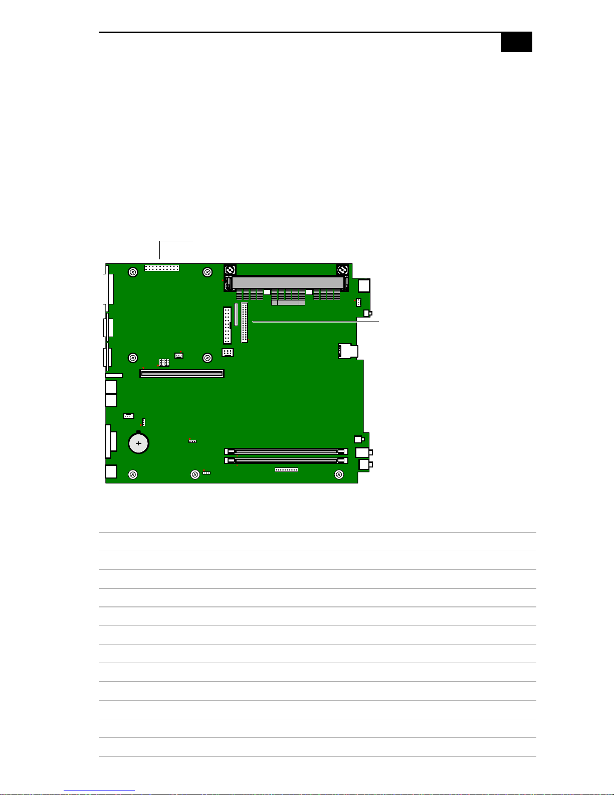
System Board
D
39
IDE Connectors
There are two IDE (Integrated Drive Electronics) connectors: a Primary
IDE and a Secondary IDE connector.
The Primary IDE connector is a 40-pin 2.54mm pitch header-type
connector for the 3.5 inch hard disk drive.
The Secondary IDE connector is a 50-pin 2mm pitch header-type
connector for the slim notebook-type CD-ROM drive.
Primary IDE
Secondary IDE
IDE Primary connector
Pin Signal
1 Reset IDE
2GND
3 Data 7
4 Data 8
5 Data 6
6 Data 9
7 Data 5
8 Data 10
9 Data 4
10 Data 11
11 Data 3
OM04701G.VS
Page 48

40
VAIO Computer Reference Manual
IDE Primary connector
Pin Signal
12 Data 12
13 Data 2
14 Data 13
15 Data 1
16 Data 14
17 Data 0
18 Data 15
19 GND
20 (Key)
21 DDRQ0
22 GND
23 I/O Write#
24 GND
25 I/O Read#
(continued)
26 GND
27 IOCHRDY
28 P_ALE (Cable Select pull-up)
29 DDACK0#
30 GND
31 IRQ 14
32 Reserved
33 Address 1
34 Reserved
35 Address 0
36 Address 2
37 Chip Select 1P#
38 Chip Select 3P#
39 Activity#
40 GND
Page 49

System Board
IDE Secondary connector
Pin Signal
1LOUT
2ROUT
3LRTN (AGND)
4RRTN (AGND)
5HRST
6HD08
7HD07
8HD09
9HD07
10 HD10
11 HD05
12 HD11
41
13 HD04
14 HD12
15 HD03
16 HD13
17 HD02
18 HD14
19 HD01
20 HD15
21 HD00
22 DMARQ
23 GND
24 HIOR#
25 HIOW#
26 GND
27 HIORDY
28 DMACK#
29 HIRQ
30 HIOCS16#
31 HA01
32 PDIAG#
33 HA00
34 HA02
Page 50

42
VAIO Computer Reference Manual
IDE Secondary connector
Pin Signal
35 HCSO#
36 HSC1#
37 DASP#
38 +5V
39 +5V
40 +5V
41 +5V
42 +5V
43 GND
44 GND
45 GND
46 GND
47 CSEL
48 GND
(continued)
49 Reserved
50 DIGITAL OUT
Page 51
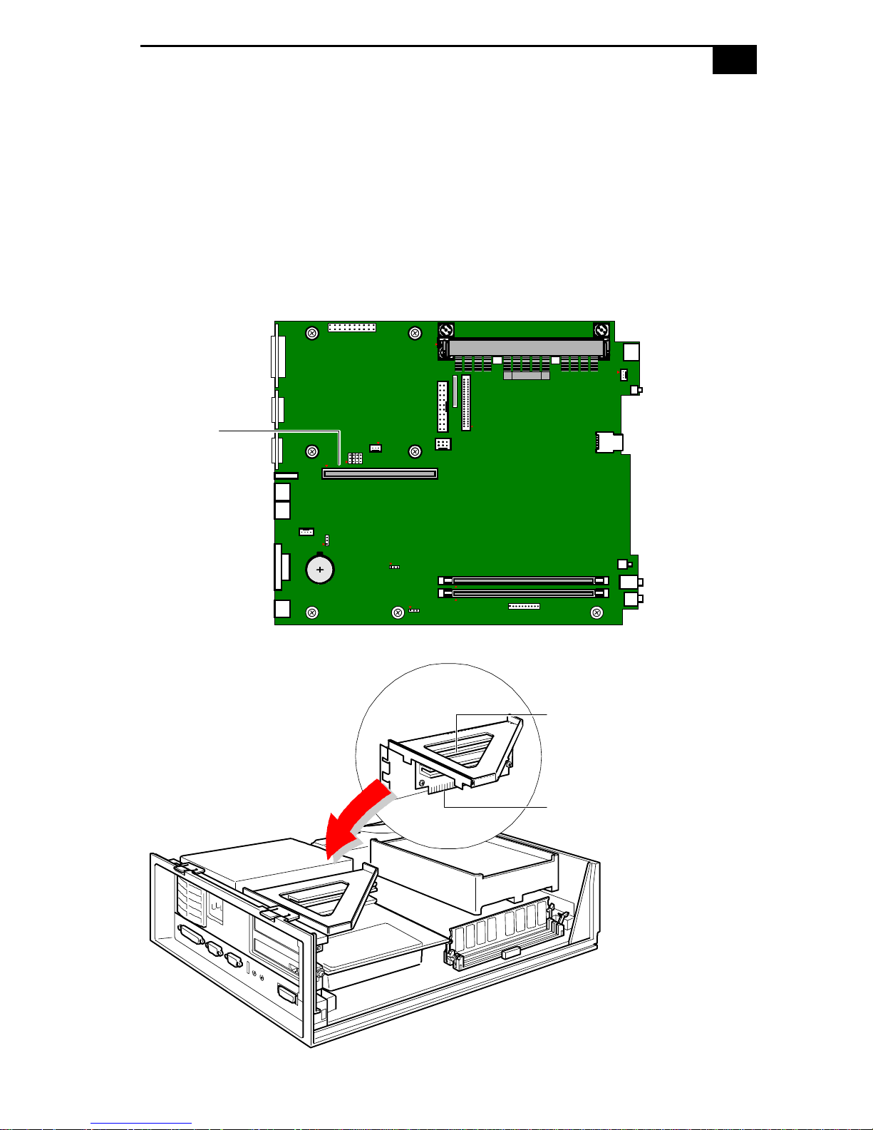
System Board
43
PCI Slot Connectors
The system board contains one PCI Riser slot connector for a PCI riser
card. The PCI riser card in turn provides two PCI slot connectors for PCI
add-in cards. One PCI slot connector is available for an add-in PCI card.
The other PCI slot connector is occupied by the fax/modem card.
The PCI slots in the riser card support 32-bit 5V and Universal (3.3/5V)
PCI add-in cards.
PCI slot for
riser card
Two PCI slot connectors
PCI riser card
(plugs into PCI connector
on system board)
OM04599B.VSD
KY0091.VSD
Page 52
44
VAIO Computer Reference Manual
PCI Riser Slot connector
*
Pin Side B Signal Side A Signal
1-12V TRST#
2TCK +12V
3 GND TMS
4 TDO TDI
5+5V +5V
6+5V INTA#
7 INTB# INTC#
8 INTD# +5V
9 PRSNT1# Reserved
10 Reserved +5V (I/O)
11 PRSNT2# Reserved
12 GND GND
13 GND GND
14 Reserved *CLK2
15 GND RST#
16 CLK1 +5V (I/O)
17 GND *GND1#
18 *REQ1# GND
19 +5V (I/O) Reserved
20 AD31 AD30
21 AD29 *GNT2#
22 GND AD28
23 AD27 AD26
24 AD25 GND
25 *REQ2# AD24
26 C/BE3# ADSEL
27 AD23 +3.3V
28 GND AD22
29 AD21 AD20
30 AD19 GND
31 +3.3V AD18
32 AD17 AD16
33 C/BE2# +3.3V
34 GND FRAME#
Page 53

System Board
45
PCI Riser Slot connector
*
Pin Side B Signal Side A Signal
35 IRDY# GND
36 +3.3V TRDY#
37 DEVSEL# GND
38 GND STOP#
39 LOCK# +3.3V
40 PERR# SDONE
41 +3.3V SBO#
42 SERR# GND
43 +3.3V PAR
44 C/BE1# AD15
45 AD14 +3.3V
46 GND AD13
47 AD12 AD11
48 AD10 GND
49 GND AD09
50 (Key) (Key)
51 (Key) (Key)
52 AD08 C/BE0#
53 AD07 +3.3V
54 +3.3V AD06
55 AD05 AD04
56 AD03 GND
57 GND AD02
58 AD01 AD00
59 +5V (I/O) +5V (I/O)
60 ACK64# REQ64#
61 +5V +5V
62 +5V +5V
* “#” means active low signal. “*” means signal is different from standard PCI. “GNT1#” means GNT#
signal for PCI slot 1. “CLK1” means signal for PCI slot 1. GNT2#” means GNT# signal for PCI slot 2.
“CLK2” means signal for PCI slot 2.
Page 54
46
VAIO Computer Reference Manual
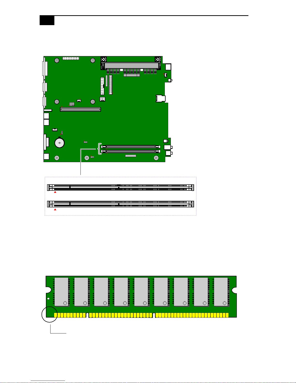
Memory Module (DIMM) Connectors
DIMM1
DIMM2
OM04710A.VSD
Both sides of each Dual Inline Memory Module (DIMM) look very
similar. The side with pin 1 has a small "1" to the left of pin 1. Be sure to
orient a DIMM correctly in the DIMM connector (a small triangle on the
connector indicates pin 1).
Memory module (DIMM)
1111
Indicates pin 1
OM04908B.VSD
Page 55
System Board
Power (ATX PWR) Connector
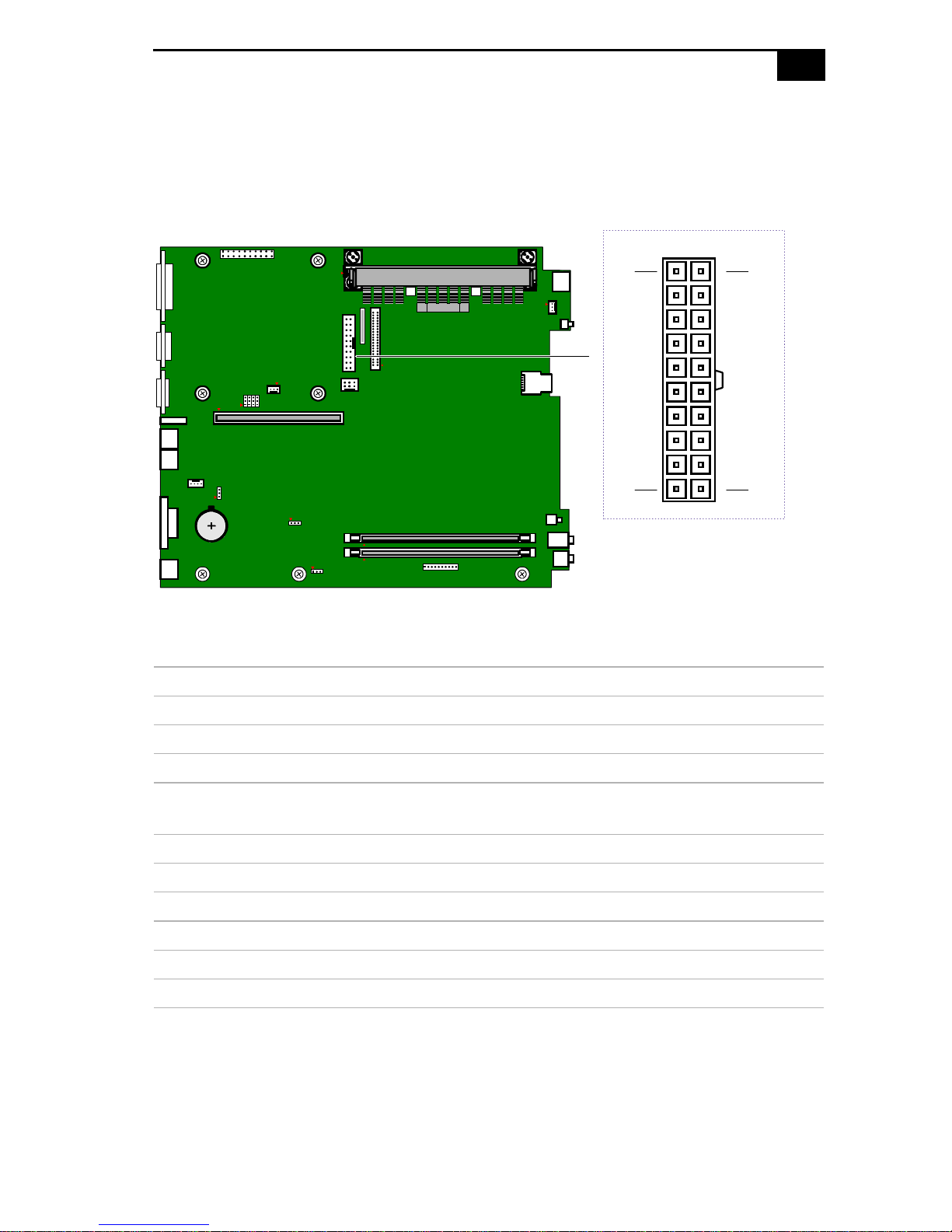
The ATX PWR connector is a 20-pin Molex-type header connector that
provides power to the ATX system board.
ATX PWR
10
20
47
1
Power connecto r
Pin # Name Pin # Name
1+3.3V 11+3.3V
2 +3.3V 12 -12V
3GND 13GND
4 +5V 14 PS- ON# (power s upply
remote on/off control)
5GND 15GND
6 +5V 16 GND
7GND 17GND
8 PWRGD (power good) 18 NC
11
OM04701I.VSD
9 +5VSB 19 +5V
10 +12V 20 +5V
Page 56
48
D
VAIO Computer Reference Manual
Fan (CPU FAN, CTRL PWR) Connectors
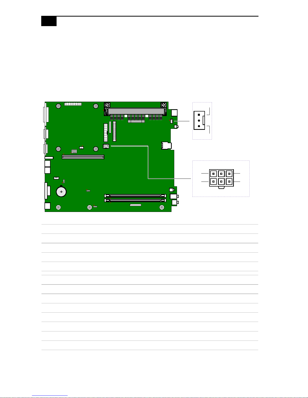
The CPU Fan connector is a 1 x 3-pin straight header connector that
controls the CPU cooling fan.
The CTRL PWR connector is a 2 x 3-pin connector that controls the power
supply cooling fan. It connects to P3 from the power supply.
CPU Fan
1
3
CTRL PWR
CPU Fan connector
Pin Signal Name
1GND
2 F AN_CTRL (+12V)
3FAN_SEN
CTRL PWR connector
Pin Signal Name
1Fan M
2Fan C
*
3 3.3V sense
1
4
3
6
KY0034.VS
4 NC (key)
5 Reserved
6 Reserved
* Power supply provides 12V to this pin when system is in Power On mode (for fastest fan speed), and 6V
when system is in Suspend mode (to redu ce fan noise).
Page 57
System Board
D
49
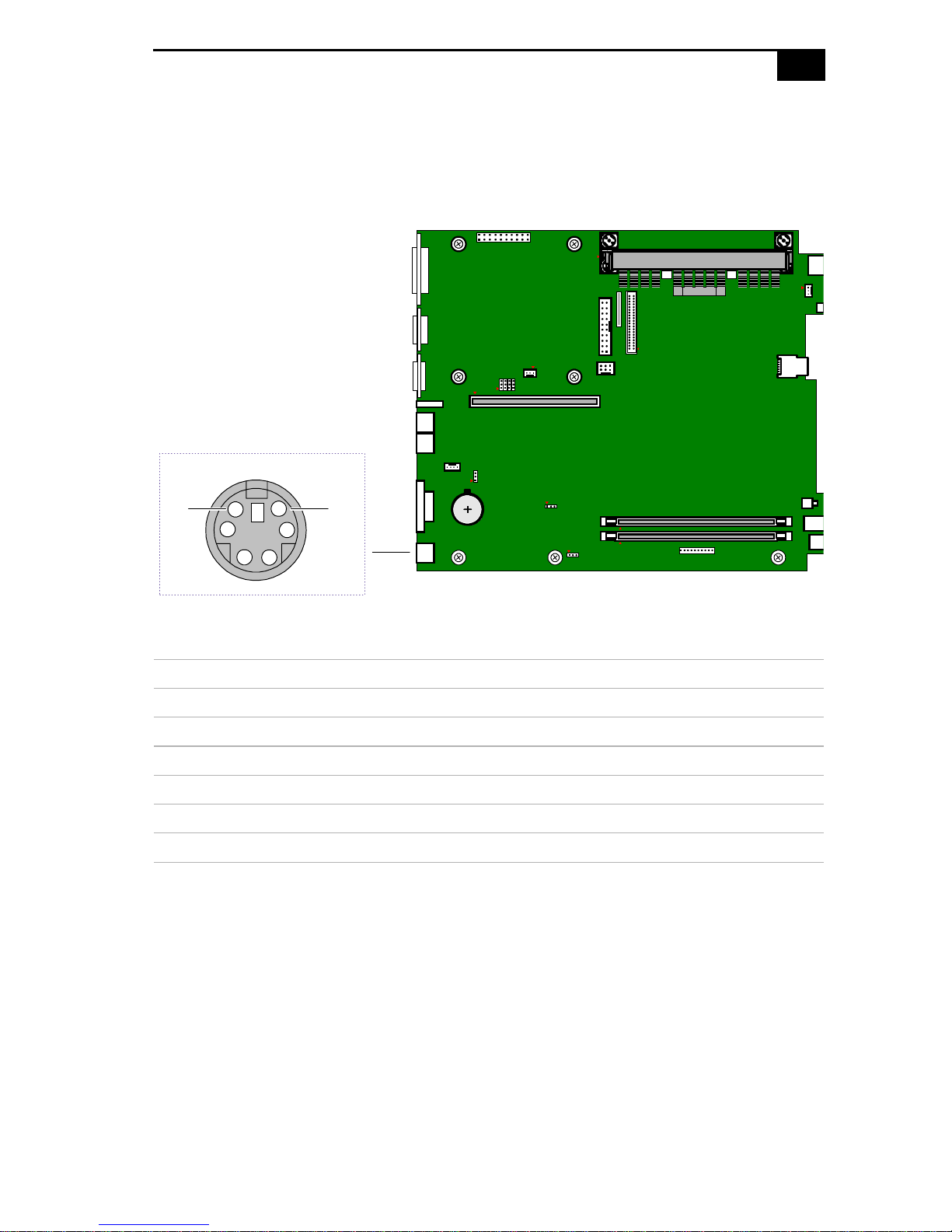
Keyboard/Mouse (KB/MOUSE) Connector
The combination keyboard/mouse connector is a 6-pin female PS/2-type
(mini-DIN) connector that can accommodate a PS/2 keyboard or mouse.
KB/MOUSE
1
6
Keyboard/Mouse connector
Pin Signal Name
1 Keyboard data
2 Mouse data
3GND
4 +5V (fused)
5 Keyboard Clock
6 Mouse Clock
KY0032.VS
Page 58
50
D
VAIO Computer Reference Manual
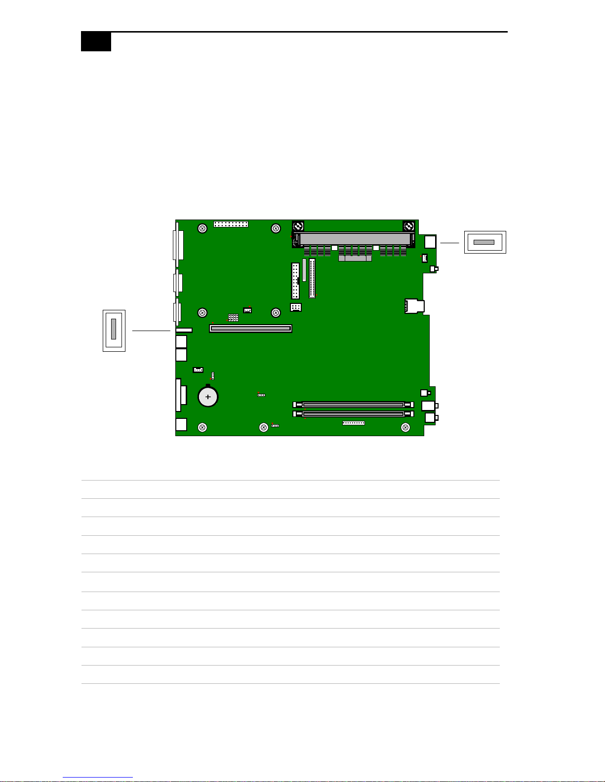
USB Connectors
There are two USB ports that permit connection of two USB peripheral
devices directly to the system without having to use an external hub. If
more USB devices are needed, connect an external hub to either USB1 or
USB2.
USB1 is a standard USB connector accessible from the rear panel. USB2 is
a standard USB connector accessible from the front panel.
USB1
USB2
USB1 connector (rear panel)
Pin Signal Name
1Power
2USBP0#
3USBP0
4GND
USB2 connector (front panel)
Pin Signal Name
1Power
2USBP1#
3USBP1
4GND
KY0033.VS
Page 59
System Board
51
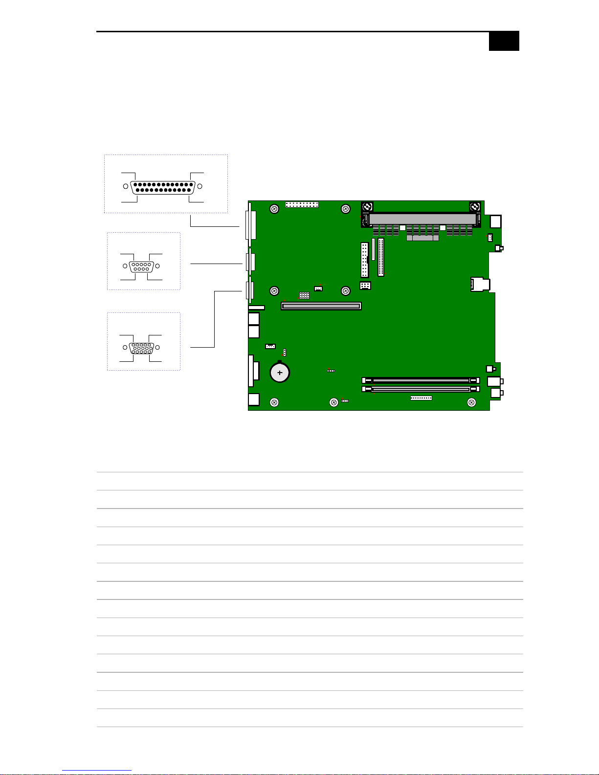
Printer, Serial, and VGA Monitor Connectors
The Serial connector is a DB-9 male connector. The Printer connector is a
DB-25 female connector. The VGA Monitor connector is a 15-pin D-sub
female connector.
13 1
25 14
15
69
VGA MONITOR
51
15 11
PRINTER
SERIAL
OM04701D.VSD
Printer connector
Pin Signal Name Pin Signal Name
1 STRO BE# 14 AUTO FEED#
2 DATA BIT 0 15 FAULT#
3 DATA BIT 1 16 INIT#
4 DATA BIT 2 17 SLCT IN#
5DATA BIT 3 18GND
6DATA BIT 4 19GND
7DATA BIT 5 20GND
8DATA BIT 6 21GND
9DATA BIT 7 22GND
10 ACK# 23 GND
11 BUSY 24 GND
12 ERROR 25 GND
13 SELECT
Page 60

52
VAIO Computer Reference Manual
Serial 1 connector
Pin Signal Name
1DCD
2 RXD#
3 TXD#
4 DTR#
5GND
6DSR
7RTS
8CTS
9RI
VGA Monitor connector
Pin Signal Name
1RED
2GREEN
3BLUE
4GND
5 DDC GND
6RED GND
7GREEN GND
8 BLUE GND
9NC
10 GND
11 GND
12 SDA
13 HORIZONTAL SYNC
14 VERTICAL SYNC
15 SCL
Page 61
System Board
53
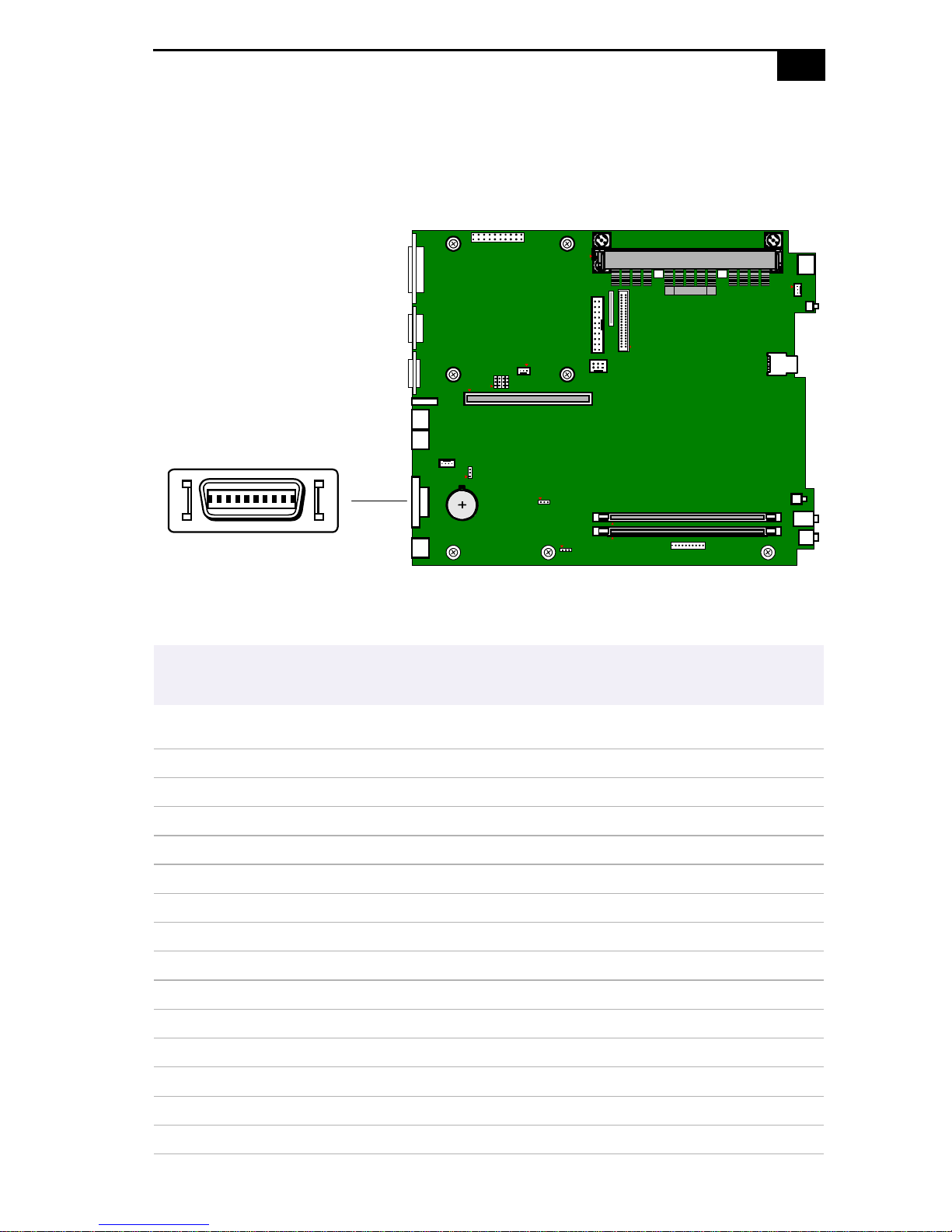
LCD Monitor Connector (VAIO Slimtop LCD models only)
The LCD monitor connector is a 26- pin M DR-type connec tor f or the Sony
VAIO Slimtop LCD monitor.
LCD Monitor
! Do not connect any other LCD monitor other than the Sony VAIO Slimtop LCD
monitor.
LCD Monitor connector
Pin Signal Pin Sig nal
1POWER GND 14TxOUT0 2 TxOUT0GND 15 TxOUT0 +
3 POWLED anode 16 SUSLED anode
4 TxOUT1 - 17 TxOUT1GND
5 TxOUT1 + 18 PVDDON
6 TxOUT2 - 19 TxOUT2GND
7 TxOUT2 + 20 Reserved
8 DETECT# 21 MSGLED#
9 BLON 22 TxCLKOUT 10 TxCLKOUTGN D 23 TxCLKOUT +
KY0094.VSD
11 POWER +12V (Fused, 1A) 24 POWER +12V (Fused, 1A)
12 Audio R 25 Audio GND
13 Audio L 26 POWER GND
Page 62
54
VAIO Computer Reference Manual
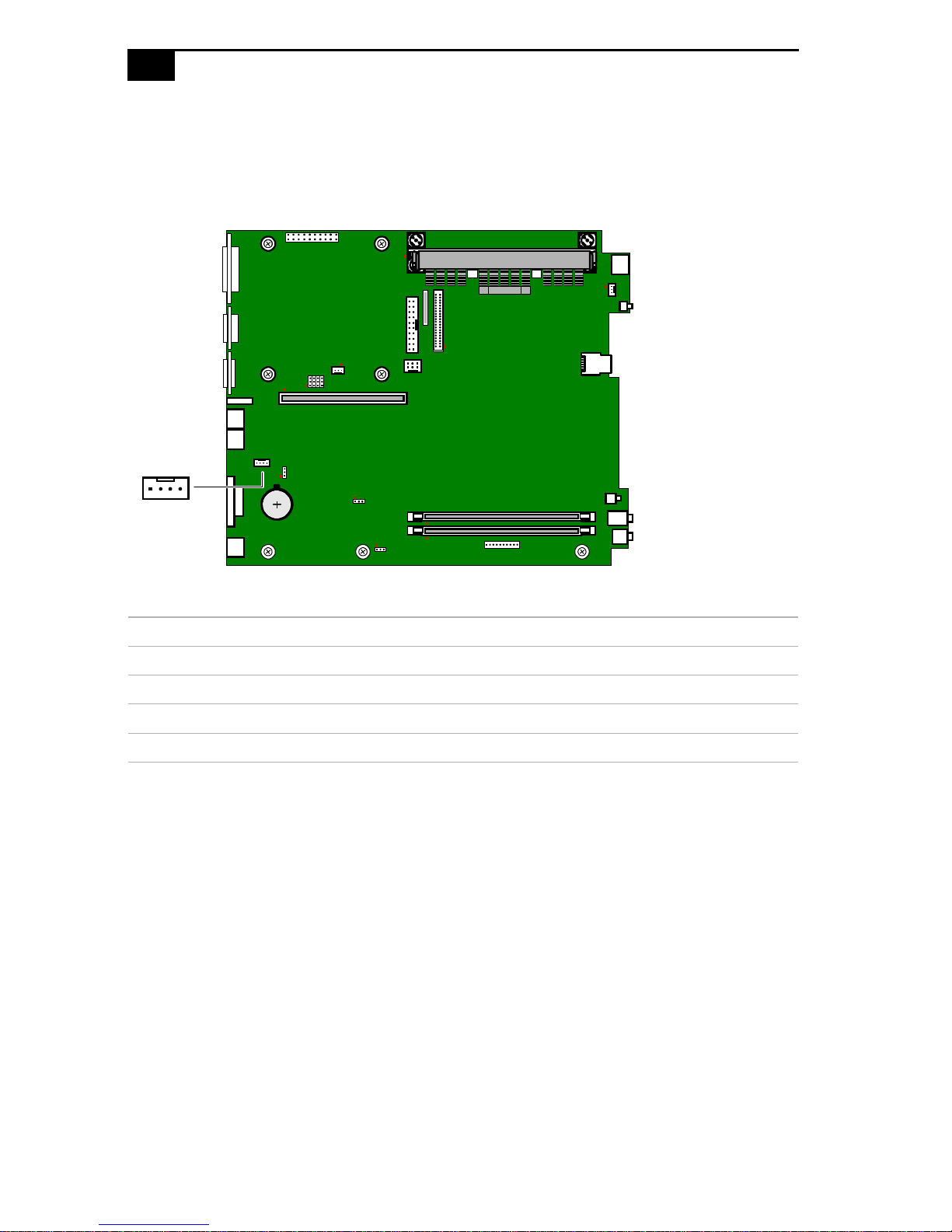
Auxiliary (AUX) Connector
The AUX connector is a standard 4-pin ATAPI-style 2.54 mm single line
header connector for external audio sound input.
AUX
14
AUX connector
Pin Signal
1 Left Line In
2GND
3GND
4 Right Line In
KY0095.VSD
Page 63
System Board
55
Wake On LAN (WOL_CON) Connector
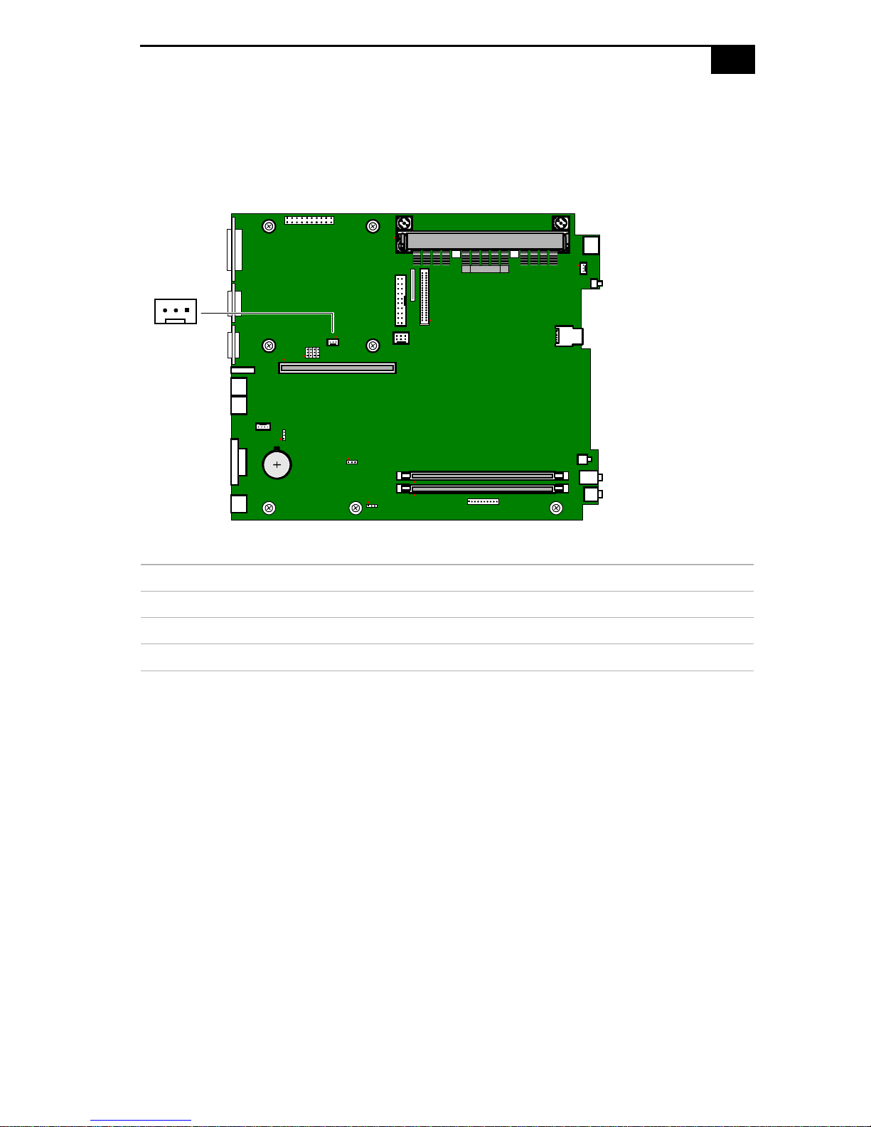
The WOL_CON connector is a 3-pin header connector that provides the
Wake On LAN function.
WOL_CON
13
Wake On LAN connector
Pin Signal
1+5V SB
2GND
3WOL signal
KY0096.VSD
Page 64
56
VAIO Computer Reference Manual
Line In and Line Out Connectors
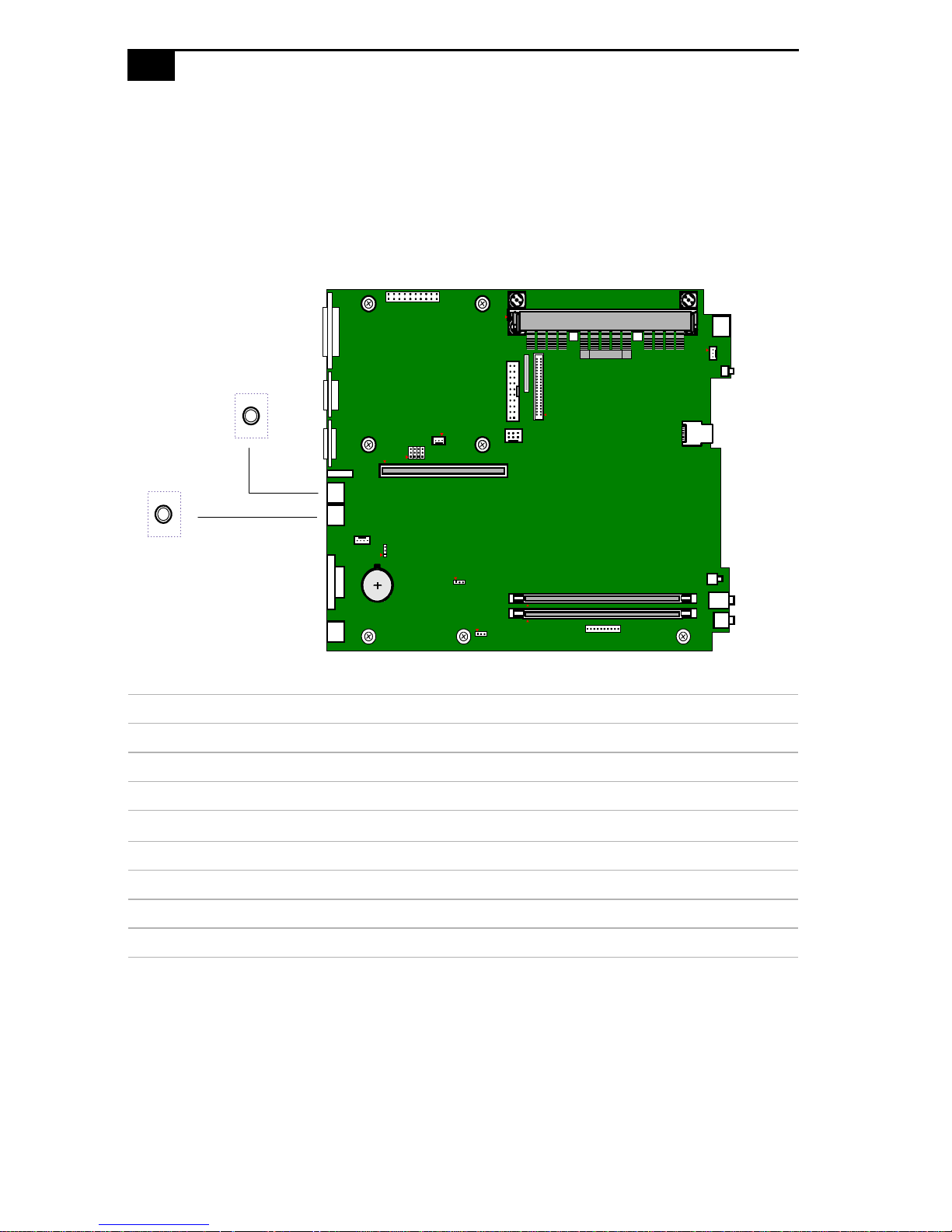
The Line In and Line Out jacks are ster eo mini-j acks (3.5 mm) that connect
to a stereo audio device (not an audio source from a video device).
Connect a stereo audio output jack to the Line In jack, and the Line Out
jack to a s tereo audio input jack.
Line In
Line Out
Line In jack
Pin Signal
Sleeve GND
Tip Audio-Left In
Ring Audio-Right In
Line Out jack
Pin Signal
Sleeve GND
Tip Audio-Left Out
Ring Audio-Right Out
KY0058.VSD
Page 65
System Board
57
Phones and Mic Connectors
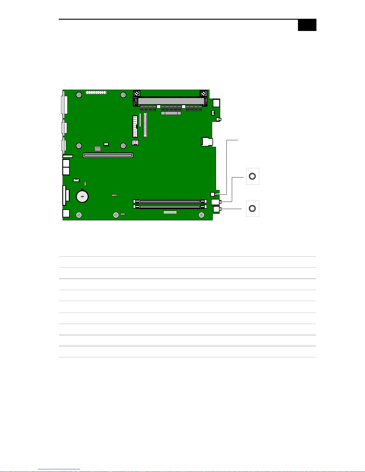
The Phones jack is stereo mi ni-jack (3.5 mm) that connects to headphones.
The Mic jack is a stereo mini-jack (3.5 mm) that connects to a microp hone.
Volume
control knob
Phones
Mic
Phones jack
Pin Signal
Sleeve GND
Tip Left Out
Ring Right Out
Mic jack
Pin Signal
Sleeve GND
Tip M icrophone Mono In
Ring Electret Bias Voltage
KY0058A.VSD
Page 66
58
VAIO Computer Reference Manual
Sony Memory Stick Connector
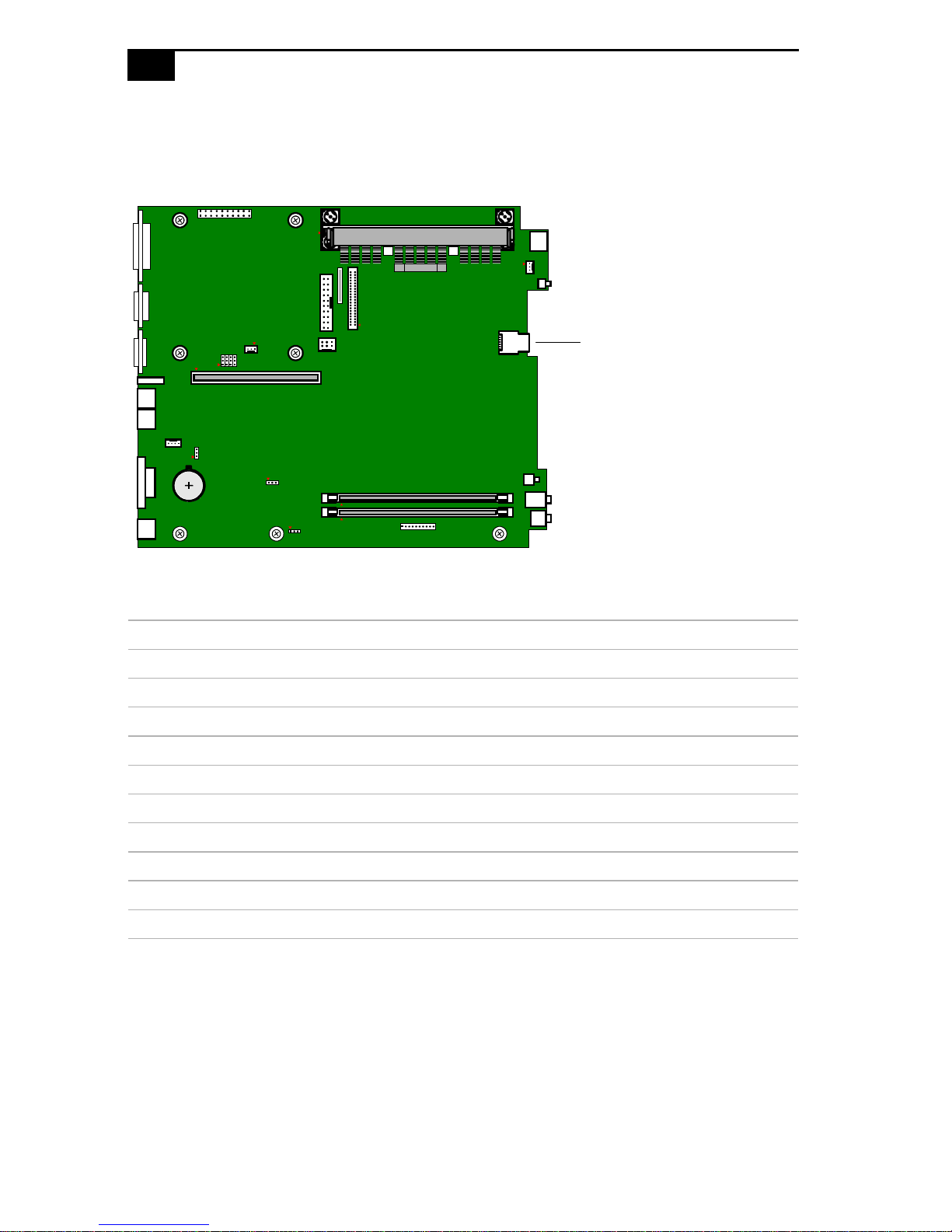
The Sony Memory Stick connector is a 10-pin MCR 103-10S connector.
Sony Memory Stick
Sony Memory Stick connector
Pin Signal
1VSS
2BS
3Reserved
4DIO
5Reserved
6 INS
7Reserved
8SCLK
9 VCC
10 VSS
KY0097.VSD
Page 67
System Board
D
59
Configuration Jumpers
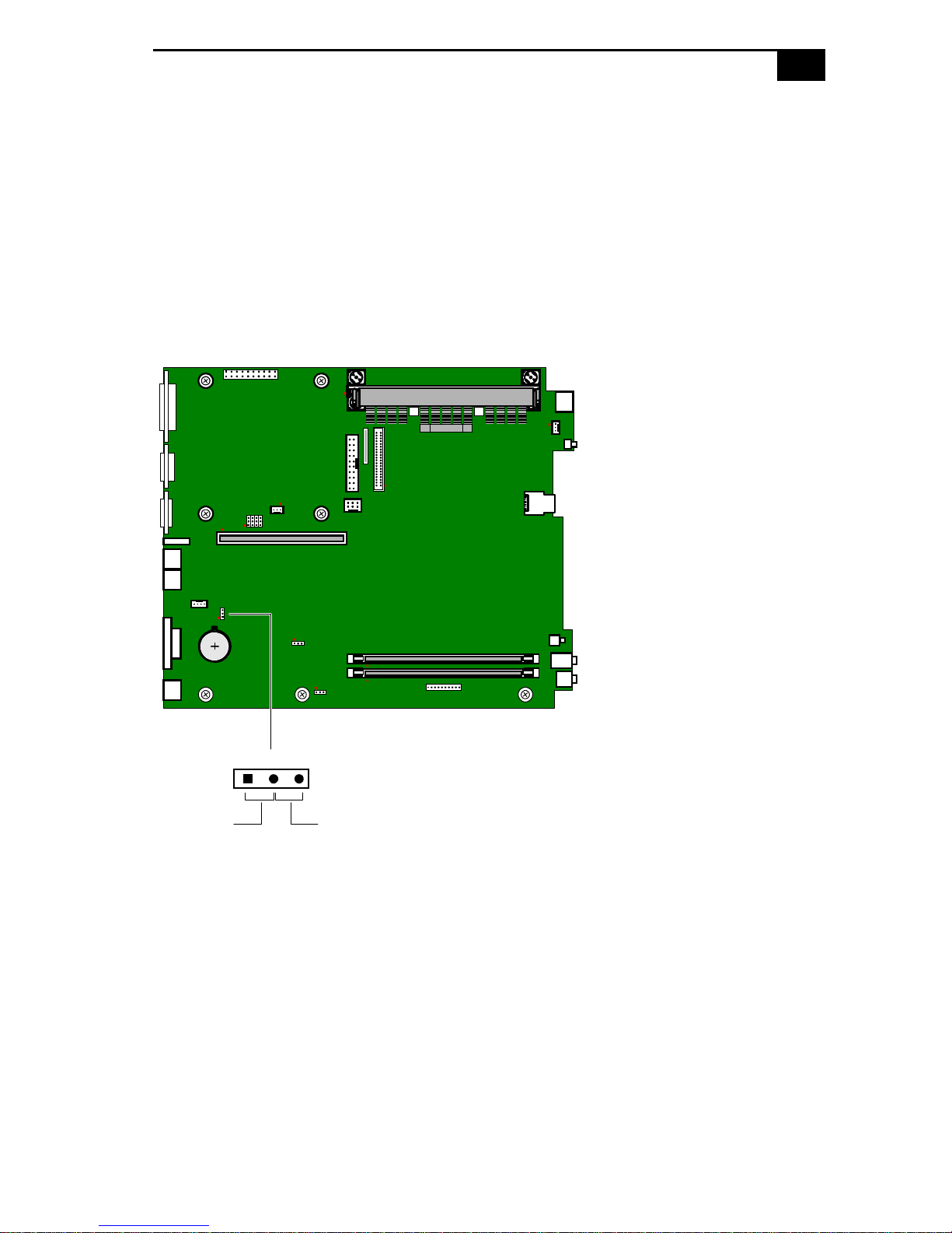
The configuration jumpers include CMOS Clear, VGA Enable, and
INTEN.
CMOS Clear (CMOS)
A jumper cap is installed on pins 2 and 3 (Normal) of the CMOS header
when the computer is shipped. Do not move the jumper cap to the CMOS
Clear position unless otherwise directed by a technical support person.
CMOS Clear
123
Normal
KY0059.VS
Page 68
60
D
VAIO Computer Reference Manual
VGA Enable (VGAEN)
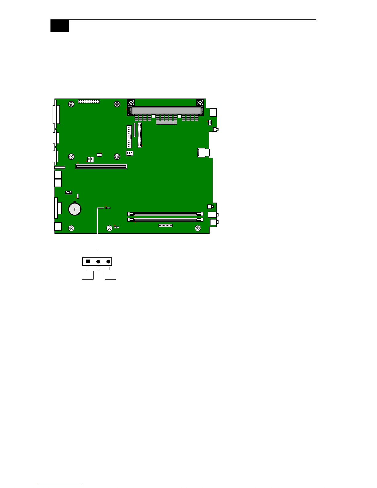
The VGAEN jumper is a 3-pin header that enables or disables the
onboard VGA controller. The computer ships with a jumper cap in the
Enable position.
VGA Enable
123
VGA Disable
KY0092.VS
Page 69
System Board
D
61
INTEN
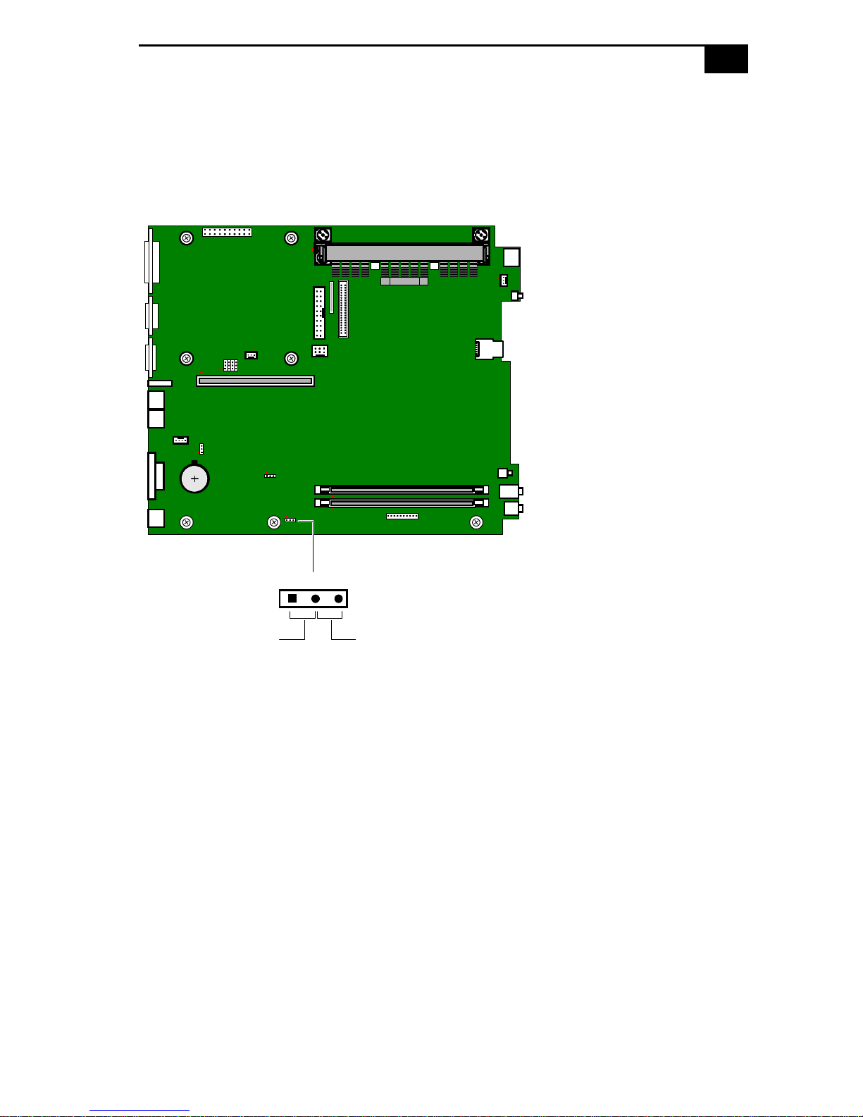
The INTEN jumper is a 3-pin header tha t ena bles or disables the onboard
VGA interrupt. The computer ships with a jumper cap in the Enable
position.
INT Enable
123
INT Disable
KY0093.VS
Page 70

62
Page 71
Chapter 5
D
Fax/Modem Card
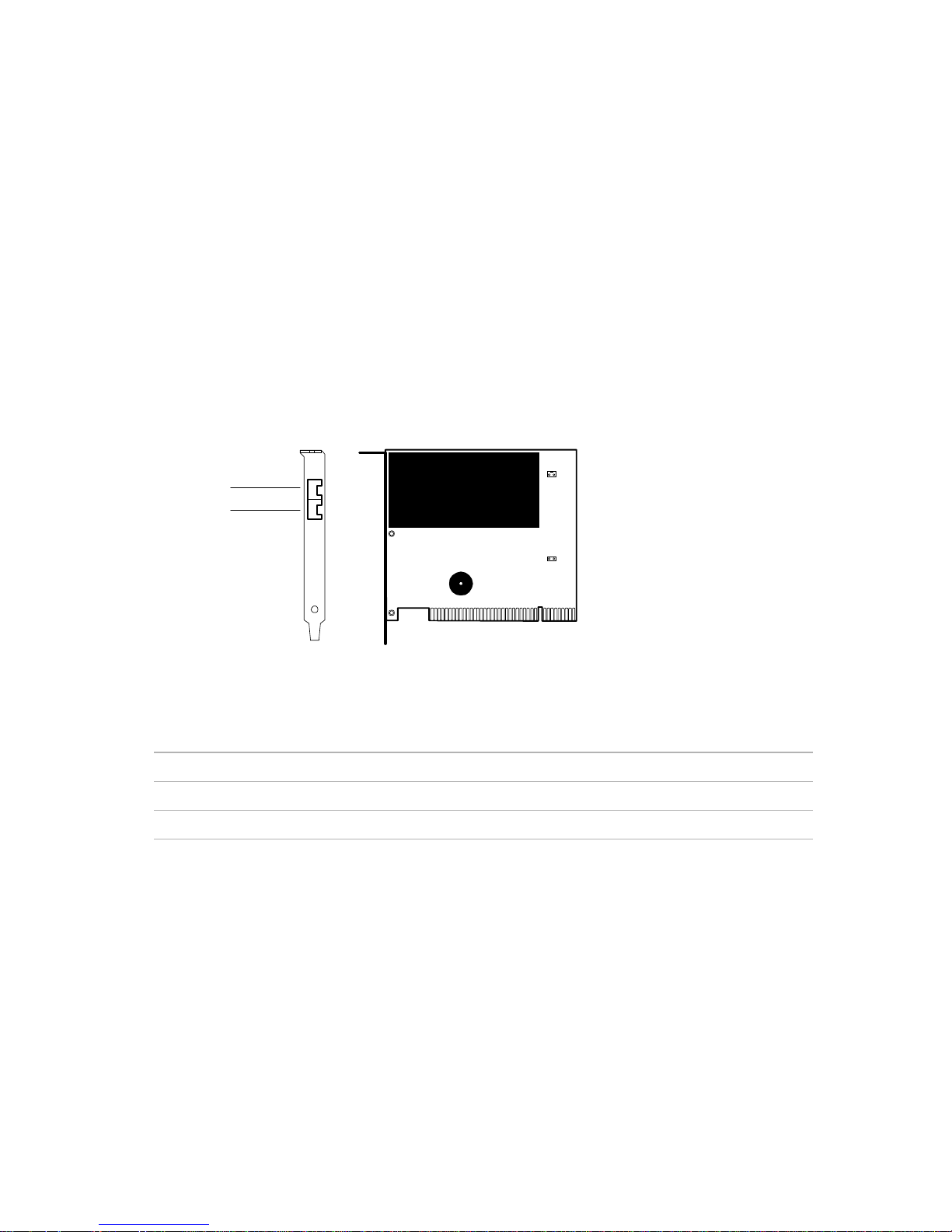
The K56flex™ technology/V.90-compatible data fax/modem card
occupies PCI slot #1 in the Riser card. The fax/modem card has two RJ-11
jacks that are accessible from the rear panel: one to connect a telephone
line, and one to connect a phone.
Telephone
Line
Connectors
Name Connector Type Description
Telephone RJ-11 Connects to phone
Line RJ-11 Connects to telephone line
KY0038.VS
63
Page 72

64
Page 73

Chapter 6
CMOS Setup Options
This chapter describes each screen in the CMOS SETUP UTILITY (see
“Accessing the CMOS Setup Utility” on page 14).
The CMOS Setup Utility presents the following menu items on the main
screen:
❑ STANDARD CMOS SETUP
❑ BIOS FEATURES SETUP
❑ CHIPSET FEATURES SETUP
❑ POWER MANAGEMENT SETUP
❑ PNP AND PCI SETUP
❑ LOAD BIOS DEFAULTS
❑ LOAD SETUP DEFAULTS
❑ SUPERVISOR PASSWORDS
❑ USER PASSWORD
❑ IDE HDD AUTO DETECTION
❑ SAVE & EXIT SETUP
❑ EXIT WITHOUT SAVING
Use the arrow keys to choose a menu item. Press Enter to display the
item’s options. Use the arrow keys to select an option. Use the Page Up or
Page Down keys to mo dify a setting.
Press Esc to go back to the main menu. Press F10 to save the changes and
exit, or press Esc to discar d the changes. Follow the on -screen prompts for
other choices. The bottom of the screen presents a summary of the
keyboard keys to use for navigation and control.
The current setting is shown in [brackets] unless the item cannot be
modified. Items beneath the current setting indicate available settings.
65
Page 74

66
VAIO Computer Reference Manual
STANDARD CMOS SETUP Screen
Date (mm:dd:yy): [Mar 15 1999]
Time (hh:mm:ss): [15:45:56]
HARD DISKS
Primary Master:
Primary Slave:
Secondary Master:
Secondary Slave:
Type [Auto]
User
None
Mode [NORMAL]
LBA
LARGE
Drive A: [1.44M, 3.5 in.]
2.88M, 3.5 in.
None
360K, 5.2 5 in.
1.2M, 5.25 in.
720K, 3.5 in.
Drive B: [None]
360K, 5.2 5 in.
1.2M, 5.25 in.
720K, 3.5 in.
1.44M, 3.5 in.
2.88M, 3.5 in.
Floppy 3 Mode Support: [Disabled]
Drive A
Drive B
Both
Video: [EGA/VGA]
CGA 40
CGA 80
MONO
Halt On: [All Errors]
No Errors
All, But Keyboard
All, But Diskette
All, But Disk/Key
Page 75

CMOS Setup Options
BIOS FEATURES SETUP Screen
CPU Internal Core Speed: 400MHz
Boot Virus Detection: [Enabled]
Disabled
CPU Level 1 Cache: [Enabled]
Disabled
CPU Level 2 Cache: [Enabled]
Disabled
CPU Level 2 Cache ECC Check: [Disabled]
Enabled
BIOS Update: [Enabled]
Disabled
Turbo Mode: [Disabled]
Enabled
67
Quick Power On Self Test: [Enabled]
Disabled
HDD Sequence SCSI/IDE First: [IDE]
SCSI
Boot Sequence: [A, CDROM, C]
CDROM, C, A
D, A
E, A
F, A
C only
LS/ZIP, C
LAN, A, C
LAN, C, A
A, C
C, A
Boot Up Floppy Seek: [Disabled]
Enabled
Floppy Disk Access Control: [R/W]
Read Only
IDE HDD Block Mode Sectors: [HDD MAX]
Disabled
2
4
8
16
32
Page 76

68
VAIO Computer Reference Manual
HDD S.M.A.R.T. capability: [Disabled]
Enabled
OS/2 Onboard Memory > 64M: [Disabled]
Enabled
Silent Boot: [Enabled]
Disabled
Boot Up Sound: [Enabled]
Disabled
Boot Up Volume:
*
[Medium]
High
Mute
Low
PCI/VGA Palette Snoop: [Disabled]
Enabled
Video ROM BIOS Shadow: [Enabled]
Disabled
C8000 - CBFFF Shadow: [Disabled]
Enabled
CC000 - CFFFF Shadow: [Disabled]
Enabled
D0000 - D3FFF Shadow: [Disabled]
Enabled
D4000 - D7FFF Shadow: [Disabled]
Enabled
D8000 - DBFFF Shadow: [Disabled]
Enabled
DC000 - DFFF F Shadow: [Disabled ]
Boot Up NumLock Status: [Off]
Typematic Rate Setting: [Disabled]
* Becomes enabled only when Boot Up Sound is enabled.
Enabled
On
Enabled
Page 77

CMOS Setup Options
Typematic Rate (Chars/Sec): [6]
8
10
12
15
20
24
30
Typematic Delay (Msec): [250]
500
750
1000
Security Option: [System]
Setup
PS/2 Mouse Function Control: [Auto]
Enabled
69
Page 78

70
VAIO Computer Reference Manual
CHIPSET FEATURES SETUP Screen
SDRAM Configuration: [By SPD]
Disabled
7ns (143MHz)
8ns (125MHz)
SDRAM CAS Latency: [2T]
3T
SDRAM RAS to CAS Delay:
*
[2T]
3T
SDRAM RAS Precharge Time:
*
[2T]
3T
DRAM Idle Timer:
*
[10T]
12T
16T
32T
Infinite
0T
2T
4T
8T
SDRAM MA Wait State: [Normal]
Slow
Fast
Snoop Ahead: [Enabled]
Disabled
Host Bus Fast Data Ready: [Disabled]
16-bit I/O Recovery Time: [1 BUSCLK]
8-bit I/O Recovery Time: [1 BUSCLK]
* These settings depend on the setting in SDRAM Configuration, and become enabled only when
SDRAM Configuration is Disabled.
Enabled
2 BUSCLK
3 BUSCLK
4 BUSCLK
2 BUSCLK
3 BUSCLK
4 BUSCLK
5 BUSCLK
6 BUSCLK
7 BUSCLK
8 BUSCLK
Page 79

CMOS Setup Options
Graphics Aperture Size: [ 64MB]
128MB
256MB
4MB
8MB
16MB
32MB
Video Memory Cache Mode: [UC]
USWC
PCI 2.1 Support: [Enabled]
Disabled
Memory Hole At 15M-16M: [Disabled]
Enabled
DRAM are 64 (Not 72) bits wide
Data Integrity Mode: Non-ECC
71
Onboard FDC Controller: [Enabled]
Disabled
Onboard FDC Sw ap A & B: [No Swap]
Swap AB
Onboard Serial Port 1: [3F8H/IRQ4]
2F8H/IRQ3
3E8H/IRQ4
2E8H/IRQ10
Disabled
Onboard Serial Port 21: [2F8H/IRQ3]
3E8H/IRQ4
2E8H/IRQ10
Disabled
3F8H/IRQ4
Onboard Parallel Port: [378H/IRQ7]
278H/IRQ5
Disabled
3BCH/IRQ7
Parallel Port Mode: [Normal]
EPP
ECP
ECP+EPP
ECP DMA Select:
* Enabled when Parallel Port Mode is ECP or ECP+EPP.
*
[3]
1
Page 80

72
VAIO Computer Reference Manual
Onboard PCI IDE Enable: [Both]
Primary
Secondary
Disable
IDE Ultra DMA Mode: [Auto]
Disable
IDE0 Master PIO/DMA Mode:
IDE0 Slave PIO/DMA Mode:
IDE1 Master PIO/DMA Mode:
IDE1 Slave PIO/DMA Mode: [Auto]
0/0
1/0
2/0
3/1
4/2
Page 81

CMOS Setup Options
POWER MANAGEMENT SETUP Screen
Power Management: [User Define]
Disable
Min Saving
Max Saving
Video Off Option: [Suspend -> Off]
Always On
Video Off Method: [DPMS OFF]
DPMS Reduce ON
Blank Screen
V/H SYNC+ B lank
DPMS Standby
DPMS Suspend
** PM Timers **
HDD Power Down: [Disable]
1 Min
2 Min
3 Min
4 Min
5 Min
6 Min
7 Min
8 Min
9 Min
10 Min
11 Min
12 Min
13 Min
14 Min
15 Min
73
Suspend Mode:
* Enabled only when Power Management is not Disable.
*
[Disable]
30 Sec
1 Min
2 Min
4 Min
8 Min
20 Min
30 Min
40 Min
1 Hour
Page 82

74
VAIO Computer Reference Manual
** Power Up Control **
PWR Button < 4 Secs: [Soft Off]
Suspend
PWR Up On Modem Act: [Enabled]
Disabled
Automatic Po w e r Up : [Disab l ed ]
Everyday
By Date
Time (hh:mm:ss) Alarm:
Date Of Month Alarm:
†
*
[17:32: 0]
[1]
.
.
.
31
** Fan Monitor **
CPU Fan Speed: [5273RPM]
Ignore
Power Fan Spe ed: [4017]
Ignore
** Thermal Monitor **
CPU Temperature: N/A
MB Temperature: [32°C/89°F]
Ignore
** Voltage Monitor **
VCORE Voltage: [2.0V]
+3.3V Voltage: [3.3V]
+5V Voltage: [5.1V]
+12V Voltage: [11.7V]
-12V Voltage: [-12.2V]
* Displays only when Automatic Power Up is Everyday or By Date.
† Displays only when Automatic Power Up is By Date.
Ignore
Ignore
Ignore
Ignore
Ignore
Page 83

CMOS Setup Options
PNP AND PCI SETUP Screen
PNP OS Installed: [No]
Yes
Slot 1 IRQ:
Slot 2 IRQ: [Auto]
NA
3
4
5
7
9
10
11
12
14
15
PCI Latency Timer: [32] PCI Clock
.
.
.
255 PCI Clock
0 PCI Clock
1 PCI Clock
.
.
.
31 PCI Clock
75
IRQ 3 Used By ISA: [No/ICU]
Yes
IRQ 4 Used By ISA: [No/ICU]
Yes
IRQ 5 Used By ISA: [Yes]
No/ICU
IRQ 7 Used By ISA: [No/ICU]
Yes
IRQ 9 Used By ISA: [No/ICU]
Yes
IRQ 10 Used By ISA: [No/I CU]
Yes
IRQ 11 Used By ISA: [No/I CU]
Yes
IRQ 12 Used By ISA: [No/I CU]
Yes
Page 84

76
VAIO Computer Reference Manual
IRQ 14 Used By ISA: [No/ICU]
Yes
IRQ 15 Used By ISA: [No/ICU]
Yes
DMA 1 Used By ISA: [No/ICU]
Yes
DMA 3 Used By ISA: [No/ICU]
Yes
DMA 5 Used By ISA: [No/ICU]
Yes
ISA MEM Block BASE: [No/ICU]
C800
CC00
D000
D400
D800
DC00
ISA MEM Block SIZE:
*
[8K]
16K
32K
64K
SYMBIOS SCSI BIOS: [Disabled]
Auto
USB IRQ: [Enabled]
Disabled
ONB VGA BIOS First: [No]
Yes
Onboard Audio: [Enabled]
Disabled]
Onboard Cardbu s: [Enabled]
Disabled
* Displays only when ISA MEM Block BASE is not No/ICU.
Page 85

CMOS Setup Options
77
LOAD BIOS DEFAULTS Screen
Press Enter to load BIOS default settings except standard CMOS setup.
LOAD SETUP DEFAULTS Screen
Press Enter to load setup defaults except standard CMOS setup.
SUPERVISOR PASSWORD Screen
Press Enter to change, s et, or disab le the supervisor password. Fo llow the prompt s.
USER PASSWORD Screen
Press Enter to change, set, or disable the user password. Follow the
prompts.
IDE HDD AUTO DETECTION Screen
Press Enter to auto-configure the hard disk drives.
SAVE & EXIT SETUP Screen
Press Enter to save c han ges in th e CMOS and exit CMOS Setup Ut ility. Follow th e
prompts.
EXIT WITHOUT SAVING Screen
Press Enter to exit CMOS Setup Utility without saving the changes. Follow the
prompts.
Page 86

78
Page 87

Chapter 7
Miscellaneous Technical
Information
This chapter contains information on the following subjects:
❑ User and Supervisor password
❑ Beep code error messages
❑ PCI configuration status and error messages
❑ DMA channel assignments
❑ IRQ assignments
❑ System I/O address map
❑ Memory map
❑ PCI configuration space map
79
Page 88
80
VAIO Computer Reference Manual
About User and Supervisor Passwords
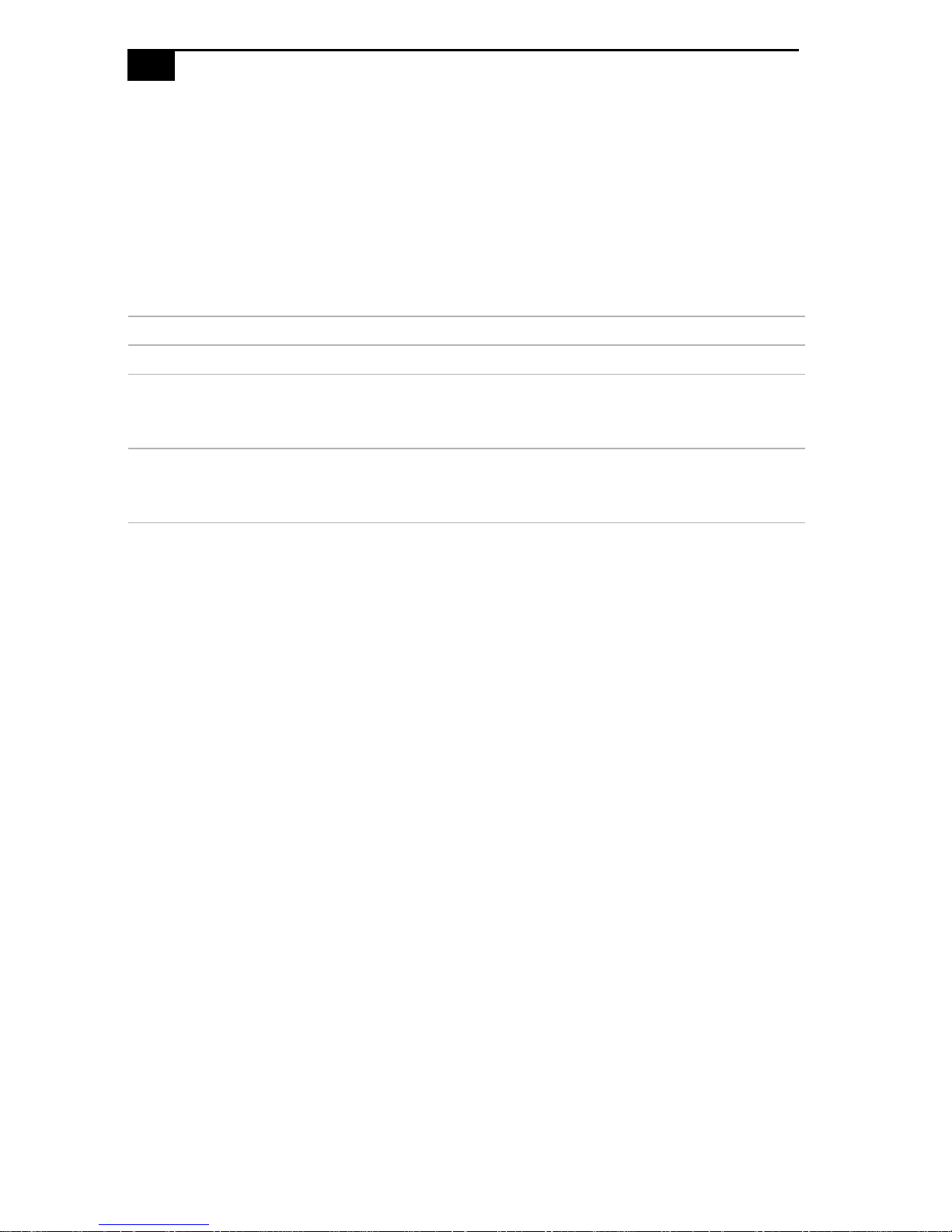
The system allows you to specify up to two passwords (a User password
and a Supervisor password) in the BIOS Setup Utility. The User password
is required; the Supervisor password is optional.
Access to the BIOS Setup Utility depends on which passwords were
previously set, as indicated next.
If you set these passwords... ...the following passwords are required:
User password only User password is required at bootup.
Supervisor password only No password is required at bootup.
Supervisor password is required by most
setup options.
Both passwords User password is required at bootup.
Supervisor password is required by most
setup options.
Page 89

Miscellaneous Technical Information
81
Beep Code Error Messages
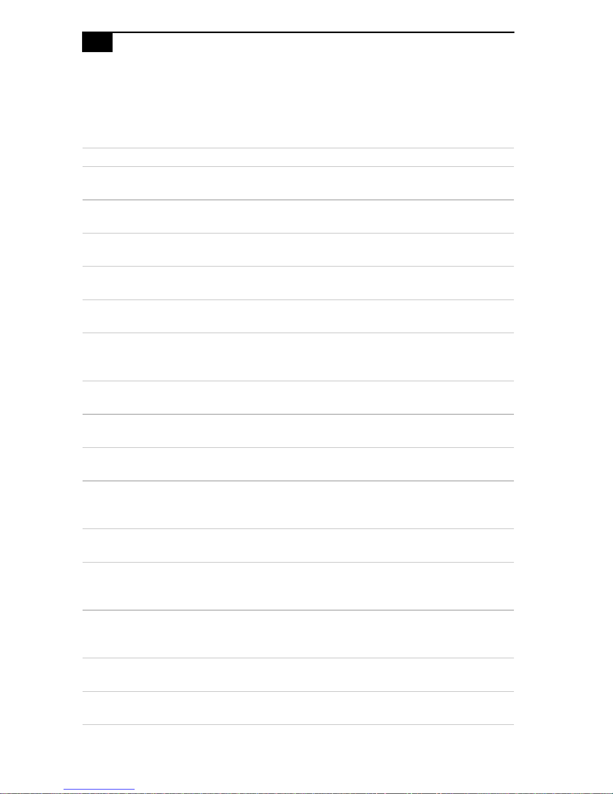
During a normal bootup, a single short beep signifies that the system is
OK. Other beep patterns signify err ors. The number of beeps indicates the
specific error that occurred.
The Sony Online Support technical representative will need to know how
many beeps your system produces if there is an error, so be sure to count
the number of beeps before calling for support.
Page 90
82
VAIO Computer Reference Manual
PCI Configuration Status and Error Messag es
The following is a list of status and error messages that may appear on
your system from time to time.
Message Meaning
Floppy Disk Controller
Resource Conflict
NVRAM Checksum Error,
NVRAM Cleared
NVRAM Cleared By Jumper The Clear CMOS jumper block has been
NVRAM Data Invalid,
NVRAM Cleared
Parallel Port Resource Conflict The parallel port has requested a resource
PCI Error Log is Full This message is displayed when more than
PCI I/O Port Conflict Two devices requested the same resource,
PCI IRQ Conflict Two devices requested the same resource,
PCI Memory Conflict Two devices requested the same resource,
The diskette controller has requested a
resource that is already in use.
The NVRAM data was reinitialized due to
an NVRAM checksum error.
changed to the clear position.
Invalid entry in the NVRAM.
that is already in use.
15 PCI conflict errors are detected. No
additional PCI errors can be logged.
resulting in a conflict.
resulting in a conflict.
resulting in a conflict.
Primary Boot Device Not
Found
Primary IDE Controller
Resource Conflict
Primary Input Device Not
Found
Primary Output Device Not
Found
Secondary IDE Controller
Resource Conflict
Serial Port 1 Resource Conflict Serial port 1 has requested a resource that is
The designated primary boot device (hard
disk drive, diskette drive, CD- RO M driv e,
or network drive) could not be found.
The primary IDE controller has requested a
resource that is already in use.
The designated primary input device
(keyboard, mouse, or other, if input is
redir ec ted ) could not be found.
The designated primary output device
(display, serial port, or other, if input is
redir ec ted ) could not be found.
The secondary IDE controll er has requested
a resource that is already in use.
already in use.
Page 91

Miscellaneous Technical Information
Static Device Resource Conflict A non-Plug and Play ISA card has
requested a res ourc e that is already i n use.
83
System Board Device Resource
Conflict
A non-Plug and-Pla y ISA card has
requested a res ourc e that is already i n use.
Page 92
84
VAIO Computer Reference Manual
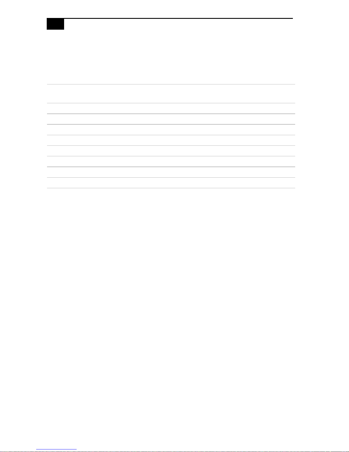
DMA Channel Assignments
This shows the factory default values. Windows 98 reassigns resources to
best meet the needs of a particular configuration.
DMA
Channel
0 Yes Open
1YesSound
2 Yes Standard diskette drive controller
3 Yes Parallel port (for ECP)
4N/AReserved
5Open
6Open
7Sound
Plug &
Play
Default
Assignment
Page 93

Miscellaneous Technical Information
IRQ Assignments
✍ This shows the factory default values. Windows 98 will reassign resources to best meet
the needs of a particular configuration. PCI IRQs can be shared between several PCI
devices.
IRQ # Default Assignment
0Interval timer
1 Keyboard buffer full
2 Cascade interrupt from slave PIC
3 COM2 (used for Sony Original Function)
4 Communications ports (COM1 and COM3)
5 PCMCIA
6 Standard diskette drive controller
85
7 Printer port (LPT1)
8 System CMOS/real time clock
9IrDA
10 Video, audio, fax/modem, user-specified
11 CardBus, USB, user-specified
12 Onboard PS/2-compatible mouse port
13 Numer ic data processor
14 Primary IDE controller
15 Secondary IDE controller
Page 94
86
VAIO Computer Reference Manual
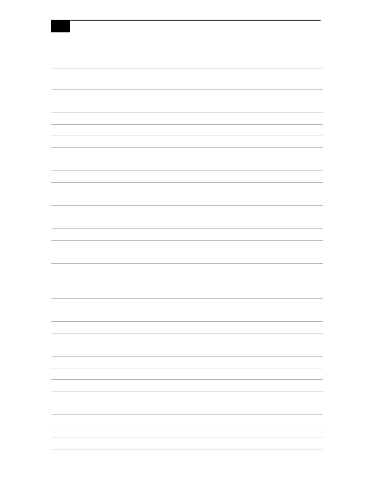
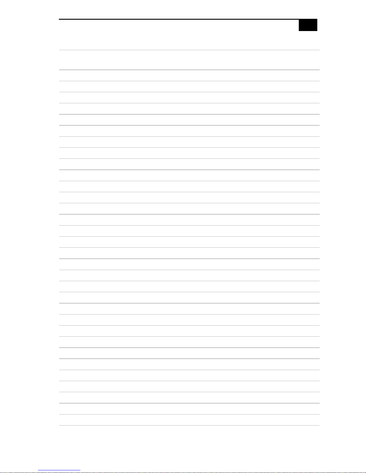
System I/O Address Map
Address Range
(hex)
0000 - 000F DMA controller 1
0020 - 0021 Programmable interrupt controller 1
002E - 002F Super I/O controller configuration registers
0040 - 0043 Counter/timer 1
0048 - 004B Counter/timer 2
0060 Keyboard controller byte - reset IRQ
0061 NMI status and s peaker controller
0064 Keyboard controller, CMD/STAT byte
0070 (bit 7) Enable NMI
0070 (bits 6:0) Real time clock, address
0071 Real time clock, data
0078 Reserved for system board configuration
0079 Reserved for system board configuration
0080 - 008F DMA page registers
Description
00A0 - 00A1 Programmable interrupt controller 2
00C0 - 00DE D MA controller 2
00F0 Clear numeric data processor error
0170 - 0177 Secondary IDE controller
01F0 - 01F7 Primary IDE controller
0201 Audio/game port controller
0220-022F Sound port (Sound Blaster compatible)
0228 - 022F LPT3
0240 - 024F Sound port (Sound Blaster compatible)
0278 - 027F LPT2
0290 - 0297 Management extension hardware
02E8 - 02EF COM4/Video (8514A)
02F8 - 02FF COM2
0300 - 0301 MPU-401 (MIDI)
0330 - 0331 MPU-401 (MIDI)
0330 - 0333 MPU-401 (MIDI)
0334 - 0335 MPU-401 (MIDI)
0376 Secondary IDE controller command port
Page 95
Miscellaneous Technical Information
87
Address Range
Description
(hex)
0377 Diskette dri ve channel 2 command port
0377 (bit 7) Diskette drive change, chan nel 2
0377 (bits 6:0) Secondary IDE controlle r status port
0378 - 037F LPT1
0388 - 038D AdLib (FM synthe sizer)
03B4 - 03B5 Video (VGA)
03BA Video (VGA)
03C0 - 03CA Video (VGA)
03CC Video (VGA)
03CE - 03CF Video (VGA)
03D4 - 03D5 Video (VGA)
03DA Video (VGA)
03E8 - 03EF COM3
03F0 - 03F5 Standard diskette drive controller, channel 1
03F6 Primary IDE channel command port
03F7 (Write) Standard diskette drive command, channel 1
03F7 (bit 7) Standard diskette disk change, channel 1
03F7 (bits 6:0) Primary IDE channel status port
03F8 - 03FF COM1
04D0 - 04D1 Edge/level-triggered PIC
0530 - 0537 Windows sound sys tem
0604 - 060B Windows sound system
LPTn + 400h ECP port, LPTn base address + 400h
0CF8 - 0CFB
†
0CF9
*
PCI configuration address register
Turbo and reset control register
0CFC - 0CFF PCI configuration data register
0E80 - 0E87 Windows sound system
0F40 - 0F47 Windows sound system
0F86 - 0F87 Yamaha OPL3-SA configuration
FF00 - FF07 IDE bus master register
FFA0 - FFA7 Primary bus master IDE registers
FFA8 - FFAF Secondary bus master IDE registers
* D word access only.
† Byte access only.
Page 96
88
VAIO Computer Reference Manual
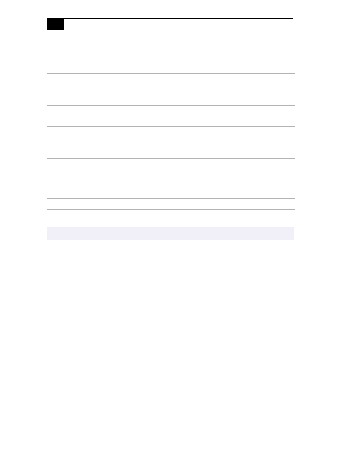
Memory Map
Address range Default configuration
001000000 - 18000000 Exte nded memory
000FC000 - 000FFFFF Boot block
000FA000 - 000FBFFF ESCD (Plug and Play configuration and DMI)
000F9000 - 000F9FFF Reserved for BIOS
000F8000 - 000F8FFF OEM Logo or Scan User Flash
000E8000 - 000F7FFF POST BIOS
000E0000 - 000E7FFF POST BIOS (available in UMB)
000C8000 - 000DFFFF Available high-DOS memory (ISA and PCI bus)
000A0000 - 000C7FFF Video memory and BIOS
0009FC00 - 0009FFFF Extended BIOS data (moveabl e by memory
manager software)
00080000 - 0009FBFF Extended conventional memory
00000000 - 0007FFFF Conventional memory
✍ I/O addresses that may be used by add-in cards are not listed.
Page 97

Miscellaneous Technical Information
PCI Configuration Space Map
89
Bus
Numbe
r (hex)
00 00 00 Intel 82440LX (PAC)
00 01 00 Intel 82440LX (PAC) AGP bus
00 07 00 Intel 82371AB (PIIX4) PCI/ISA bridge
00 07 01 Intel 82371AB (PIIX4) IDE bus master
00 07 02 Intel 82371A B (PI I X4) USB
00 07 03 Intel 82371A B (PI I X4) power
00 0D 00 PCI exp ansion slot 1
00 0E 00 PCI expansi on slot 2
01 ATI Rage LT Pro video
00 Yamaha YMF724E audio
00 Ricoh RL5C475 cardbus
00 PCI fax/modem
Device
Number
(hex)
Function
Number
(hex)
Description
management
Page 98

90
Page 99

Chapter 8
Specifications
This chapter describes the technical specifications for the Sony
PCV-L400, PCV-L600, and PCV-L600S computers.
Processors
PCV-L400 400 MHz Intel Pen tium® II processor (with 100 MHz FSB)
PCV-L600 500 MHz Intel Pen tium® III processor (with 100 MHz FSB)
PCV-L600S 500 MHz Intel Pentium® III processor (with 100 MHz FSB)
Chipset
82440BX-100 AGP/PCI/ISA chipset
PCI Bus
PCI Level 2.1, 33 MHz zero wait state
2 PCI slots (1 open)
Memory Modules (DIMMs)
Installed memory PCV-L400: 64 Mbytes SDRAM
PCV-L600/PCV-L600S: 128 Mbytes SDRAM
Maximum memory 256 Mbytes (128Mbytes in each socket)
Voltage 3.3 V memory only
Pins 168-pins with gold- plated contacts
SDRAM type PC100 (100 MHz), 60 ns, unrestricted CAS latency 3,
unbuffered, Intel 4-clock, 64 bits (non-ECC)
91
Page 100

92
VAIO Computer Reference Manual
DIMM Configurations
DIMM1
0, 16, 32, 64, 128 0, 16, 32, 64, 128
* The PCV-L400 is shipped with 64 MB. The PCV-L600 and PCV-L600S are shipped with 128 MB. SDRAM is
*
expandable to 256 MB. Computer SDRAM is unbuffered DIMM, specification Rev. 1.0 or later. Supports
SDRAM memory. Does not support EDO memory or buffered DIMM memory. Memory can be installed in
either socket. Memory size can vary between sockets. DIMMs can be single- or double-sided. DIMMs must
be 3.3V unbuffered 4-clock, 64-bit or 72-bit, 66 MHz or 100 MHz SDRAM module. Use only 100 MHz FSBsupported memory. Do not mix 66 MHz memory with 100 MHz memory.
DIMM2
*
L2 Cache
Installed 512 kbytes secondary write-back cache (in processor),
direct-mapped organization, BSB cache
Controller Intel 440BX Host Bridge/Controller
Graphics
Controller
*
ATI Rage LT Pro AGP 64-bit PCI graphics accelerator
including 1X and 2X modes with sidebands
Video memory 4 Mbytes
Resolution (displayed resolution depends on the graphics display you use)
True color (32 bit s) Up to 1920 x 108 0 at 70 Hz non-interlaced
True color (24 bit s) Up to 1920 x 108 0 at 70 Hz non-interlaced
High color (16 bits) Up to 1920 x 1200 at 70 H z non-interlaced
256 colors ( 8 bits) Up to 1920 x 1200 at 70 Hz non- interlaced
* Supports DDC-1 and DDC-2b standards for Plug and Play displays.
 Loading...