

Page 1
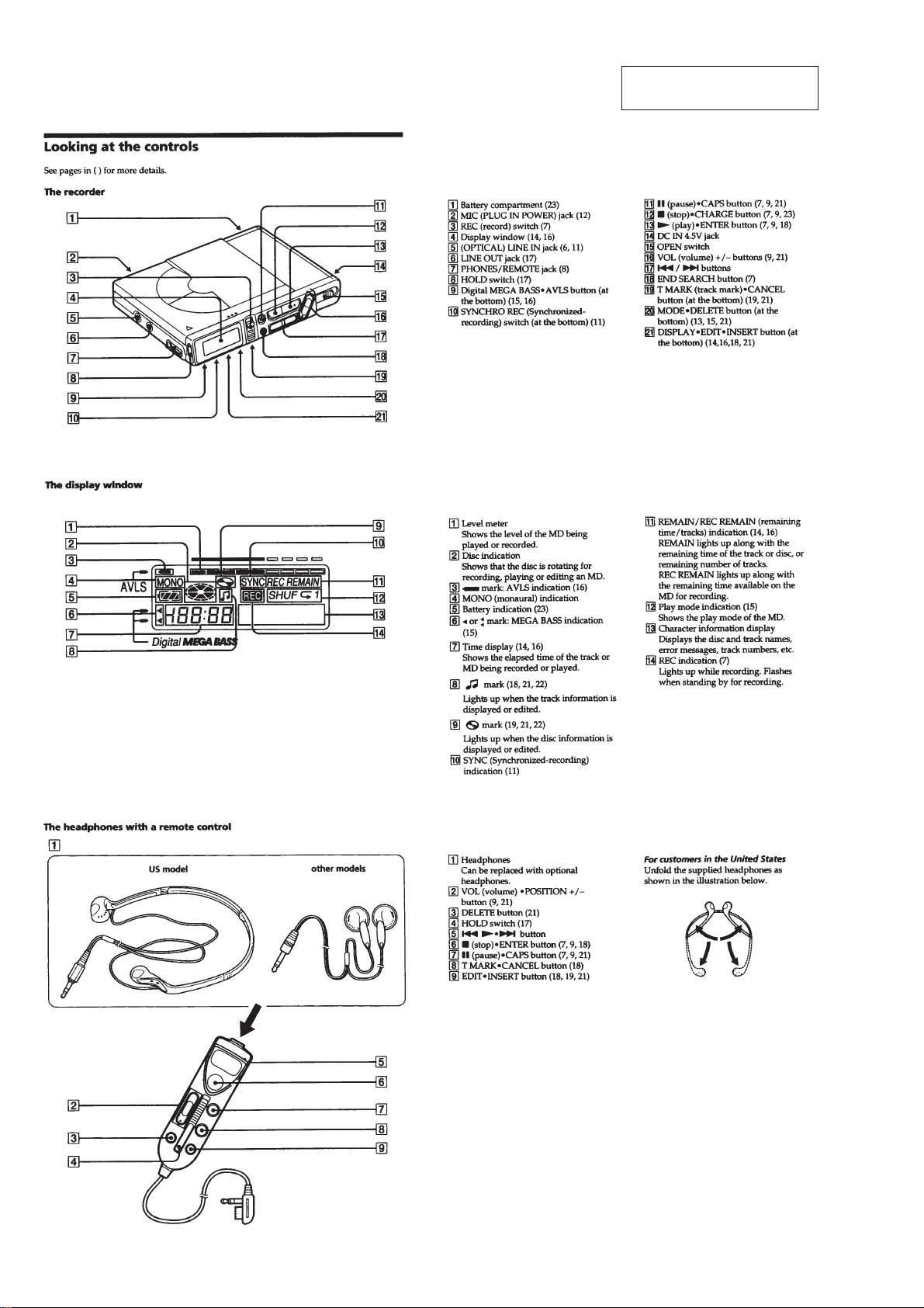
MICROFILM
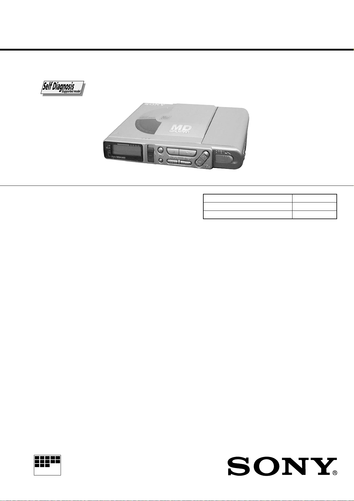
MZ-R37
SERVICE MANUAL
Ver 1.4 2001. 01
With SUPPLEMENT-1
(9-926-952-81)
With SUPPLEMENT-2
(9-926-952-82)
US and foreign patents licensed from Dolby Laboratories
Licensing Corporation.
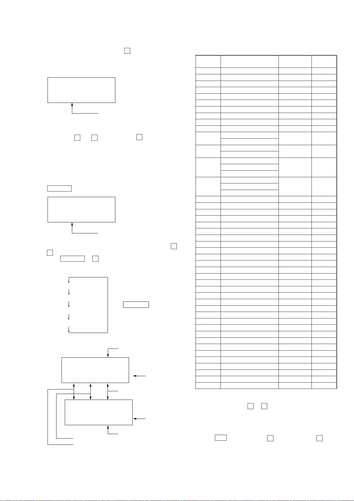
SPECIFICATIONS
System
Audio playing system
MiniDisc digital audio system
Laser diode properties
Material: GaAlAs
Wavelength: λ = 780 nm
Emission duration: continuous
Laser output: less than 44.6 µW
(This output is the value measured at a
distance of 200 mm from the lens surface on
the optical pick-up block with 7 mm
aperture.)
Recording and playback time
Maximum 74 minutes (MDW-74, stereo
recording)
Maximum 148 minutes (MDW-74, monaural
recording)
Revolutions
400 rpm to 900 rpm (CLV)
Error correction
Advanced Cross Interleave Reed Solomon
Code (ACIRC)
Sampling frequency
44.1 kHz
Sampling rate converter
Input: 32 kHz / 44.1 kHz / 48 kHz
Coding
Adaptive TRansform Acoustic Coding (ATRAC)
Modulation system
EFM (Eight to Fourteen Modulation)
Number of channels
2 stereo channels
1 monaural channel
US Model
Canadian Model
AEP Model
UK Model
E Model
Australian Model
Tourist Model
Model Name Using Similar Mechanism MZ-R55
MiniDisc Mechanism Type MT-MZR37-161
Optical Pick-up T ype KMS-280A
Frequency response
20 to 20,000 Hz ± 3 dB
Wow and Flutter
Below measurable limit
Inputs
MIC (PLUG IN POWER): stereo mini-jack,
0.35–1.38 mV
(OPTICAL) LINE IN: stereo mini-jack with
optical (digital) in
• Line in: 69–194 mV
• Optical (digital) in: wave length 660 nm
Outputs
PHONES/REMOTE: stereo mini-jack,
maximum output level 5 mW + 5 mW, load
impedance 16 ohm
LINE OUT: stereo mini-jack, 194 mV, load
impedance 10 kilohm or greater
General
Power requirements
Sony AC Power Adaptor (supplied)
connected at the DC IN 4.5 V jack:
120 V AC, 60 Hz (US, Canadian model)
220–230 V AC, 50/60 Hz (AEP model)
230–240 V AC, 50 Hz (UK model)
240 V AC, 50 Hz (Australian and New Zealand model)
Two nickel-cadmium rechargeable batteries
NC-AA (supplied)
Two LR6 (size AA) alkaline batteries (not supplied)
– Continued on next page –
PORTABLE MINIDISC RECORDER
– 1 –
Page 2
Battery operation time
Batteries Recording
Two NC-AA Approx. Approx.
nickel-cadmium
rechargeable batteries
Two LR6 (size AA) ––––
Sony alkaline dry batteries 13 hours
1)
The battery life may be shorter due to
operating conditions and the temperature
of the location.
2)
When you record, use fully charged
rechargeable batteries.
3)
Recording time may differ according to the
alkaline batteries.
Dimensions
Approx. 116.8 × 18.5 × 86.1 mm (w/h/d)
(4 5/8 × 3/4 × 3 1/2 in.)
Mass
Approx. 160 g (5.6 oz) the recorder only
Approx. 220 g (7.8 oz) incl. a recordable MD,
and two NC-AA nickel-cadmium
rechargeable batteries
Supplied accessories
Optical cable (1) (MC-918)
AC power adaptor (1) (AC-MZR37)
Headphones with a remote control (1) (SZR-S17)
NC-AA nickel-cadmium rechargeable batteries (2)
Rechargeable battery carrying case (1)
Design and specifications are subject to change without notice.
1)
3 hours 5 hours
3)
2)
Playback
Approx.
Precautions for Laser Diode Emission Check
When checking the emission of the laser diode during adjustments, never view directly downwards as this may lead to
blindness.
Precautions for Using Optical Pick-up (KMS-280A)
As the laser diode inside the optical pick-up damages by static
electricity easily, solder the laser tap of the Optical pick-up
flexible board when handling. Also take the necessary measures
to prevent damages by static electricity. Handle the Optical pickup flexible board with care as it breaks easily.
This MiniDisc player is classified as a CLASS 1 LASER
product.
The CLASS 1 LASER
PRODUCT label is located on
the bottom exterior.
IN NO EVENT SHALL SELLER BE
LIABLE FOR ANY DIRECT,
INCIDENTAL OR CONSEQUENTIAL
DAMAGES OF ANY NATURE, OR
LOSSES OR EXPENSES RESULTING
FROM ANY DEFECTIVE PRODUCT
OR THE USE OF ANY PRODUCT.
“MD WALKMAN” is a trademark of Sony
Corporation.
CAUTION
Use of controls or adjustments or performance of procedures
other than those specified herein may result in hazardous
radiation exposure.
Flexible Circuit Board Repairing
• Keep the temperature of the soldering iron around 270°C
during repairing.
• Do not touch the soldering iron on the same conductor of the
circuit board (within 3 times).
• Be careful not to apply force on the conductor when soldering
or unsoldering.
Notes on chip component replacement
• Never reuse a disconnected chip component.
• Notice that the minus side of a tantalum capacitor may be
damaged by heat.
Laser tap
Optical Pick-up flexible board
SAFETY-RELATED COMPONENT WARNING!!
COMPONENTS IDENTIFIED BY MARK ! OR DO TTED LINE WITH
MARK ! ON THE SCHEMATIC DIAGRAMS AND IN THE PARTS
LIST ARE CRITICAL TO SAFE OPERATION.
REPLACE THESE COMPONENTS WITH SONY PARTS WHOSE
PART NUMBERS APPEAR AS SHOWN IN THIS MANUAL OR IN
SUPPLEMENTS PUBLISHED BY SONY.
ATTENTION AU COMPOSANT AYANT RAPPORT
À LA SÉCURITÉ!!
LES COMPOSANTS IDENTIFIÉS P AR UNE MARQUE ! SUR LES
DIAGRAMMES SCHÉMA TIQUES ET LA LISTE DES PIÈCES SONT
CRITIQUES POUR LA SÉCURITÉ DE FONCTIONNEMENT. NE
REMPLACER CES COMPOSANTS QUE PAR DES PIÈCES SONY
DONT LES NUMÉROS SONT DONNÉS DANS CE MANUEL OU
DANS LES SUPPLÉMENTS PUBLIÉS PAR SONY.
– 2 –
Page 3
TABLE OF CONTENTS
r
1. GENERAL
Looking at the controls ...................................................... 4
2. SELF-DIAGNOSTIC
2-1. General ............................................................................... 5
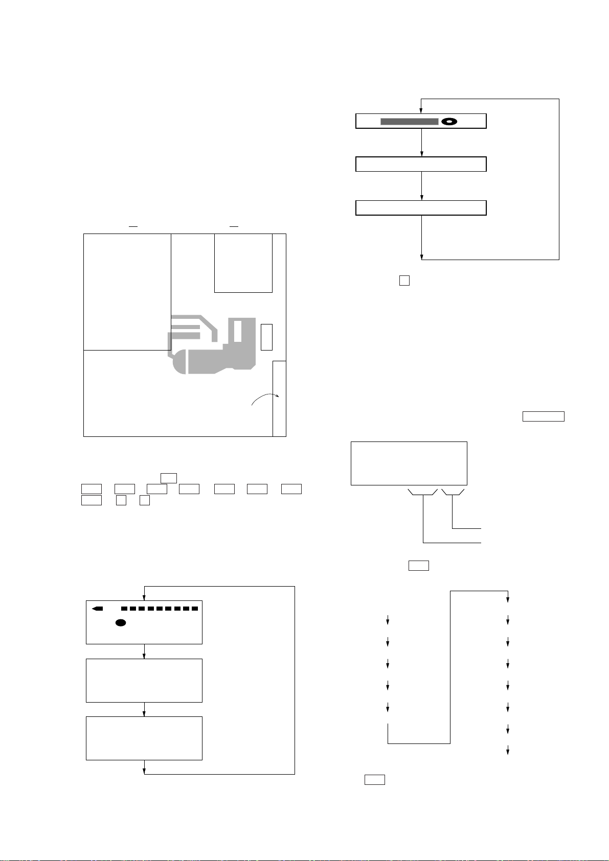
2-2. Test Mode Setting .............................................................. 5
2-3. Operation in Test Mode Setting ......................................... 5
2-4. Releasing the Test Mode .................................................... 5
2-5. Self-Diagnostic Mode ........................................................ 5
2-6. Clearing the Error Indication Code
and Total Recording Time.................................................. 6
3. DISASSEMBLY
3-1. Panel, Bottom..................................................................... 7
3-2. Panel (SV) Assy, Front ....................................................... 7
3-3. LCD Module ...................................................................... 8
3-4. Connector ........................................................................... 8
3-5. Main Board ........................................................................ 9
3-6. Panel (SV) Assy, Upper ..................................................... 9
3-7. Cabinet (SV) Assy ........................................................... 10
3-8. OP Block Assy ................................................................. 10
3-9. Holder Assy...................................................................... 11
4. TEST MODE
4-1. General ............................................................................. 12
4-2. Test Mode Setting ............................................................ 12
4-3. Test Mode Structure......................................................... 12
4-4. Manual Mode ................................................................... 12
4-5. Overall Adjustment Mode (Assy Mode).......................... 15
4-6. Hybrid Mode, Key Check Mode...................................... 16
5. ELECTRICAL ADJUSTMENTS........................... 17
6. DIAGRAMS
6-1. IC Pin Descriptions .......................................................... 20
6-2. Block Diagram – Servo Section –.................................... 25
6-3. Block Diagram – Audio Section – ................................... 27
6-4. Block Diagram – System Control Section – .................... 29
6-5. Printed Wiring Board ....................................................... 31
6-6. Schematic Diagram – Main Section (1/3) –..................... 35
6-7. Schematic Diagram – Main Section (2/3) –..................... 38
6-8. Schematic Diagram – Main Section (3/3) –..................... 41
7. EXPLODED VIEWS
7-1. Panel Section.................................................................... 49
7-2. Cabinet (SV) Assy Section .............................................. 50
7-3. Mechanism Deck Section ................................................ 51
8. ELECTRICAL PARTS LIST................................... 52
SERVICING NOTE
1) When repairing this device with the power on, if you remove
the main board or open the upper panel assy, this device stops
working.
In this case, you can work without the device stopping by
fastening the hook of the OPEN1 switch (S801) with tape.
tape
S801
panel assy, uppe
MAIN board
2) This set is designed to perform automatic adjustment for each
adjustment and write its value to EEPROM. Therefore, when
EEPROM (IC803) has been replaced in service, be sure to perform automatic adjustment and write resultant values to the new
EEPROM.
Refer to page 12 for details.
– 3 –
Page 4
SECTION 1
GENERAL
This section is extracted from
instruction manual.
– 4 –
Page 5
SECTION 2
888
ı
Vr. 1.‚‚
All ON
All OFF
Microprocessor
version
display
Error indication code
History code
1st0 00
SELF-DIAGNOSTIC
2-1. GENERAL
This set uses the self-diagnostic system in which if an error occurs
in playback/recording mode, the error is detected by the model
control and power control blocks of the microprocessor and information on the cause is stored as history in EEPROM.
By viewing this history in test mode, it helps you to analyze a fault
and determine its location.
2-2. TEST MODE SETTING
There are two different methods to set the test mode:
1 Short BP801 (TEST) on the main board with a solder bridge
(connect pin @§ of IC801 to the ground). Then, turn on the
power.
MAIN BOARD (SIDE B)
X801
IC801
25
26
BP801
(TEST)
C401
IC301
2) Remote controller LCD
• Holding down P allows the current display to be maintained
while it being depressed.
2-4. RELEASING THE TEST MODE
For test mode set with the method 1:
Turn off the power and open the solder bridge on BP801 on the
main board.
For test mode set with the method 2:
Turn off the power.
2-5. SELF-DIAGNOSTIC MODE
1. Go into the test mode.
2. With the unit LCD indicators all flashing, press DISPLA Y key
to go into the self-diagnostic mode.
2 In the normal mode, use the keys on the unit to perform the
following operations:
Press and hold down ( and press the keys below in this turn:
+ n + n =n = n + n = n + n
= n P n P
2-3. OPERATION IN TEST MODE SETTING
When the test mode is set, the LCD shows repeated cycles of the
following display:
1) Unit LCD
ı
188:88 pppppp
Vr. 1.00
All ON
All OFF
Microprocessor
version
display
3. Then, eac h time ) ke y is pressed, the reference information
display changes as given below.
1st ‚ XX
1st 1 ‚‚
1st 2 ‚‚
N ‚ XX
N 1 ‚‚
N 2 ‚‚
N-1 ‚ XX
N-1 1 ‚‚
N-1 2 ‚‚
N-2 ‚ XX
N-2 1 ‚‚
N-2 2 ‚‚
R XXXX
1st ‚ XX
• Press = key to go back to the previous display.
(return)
– 5 –
Page 6
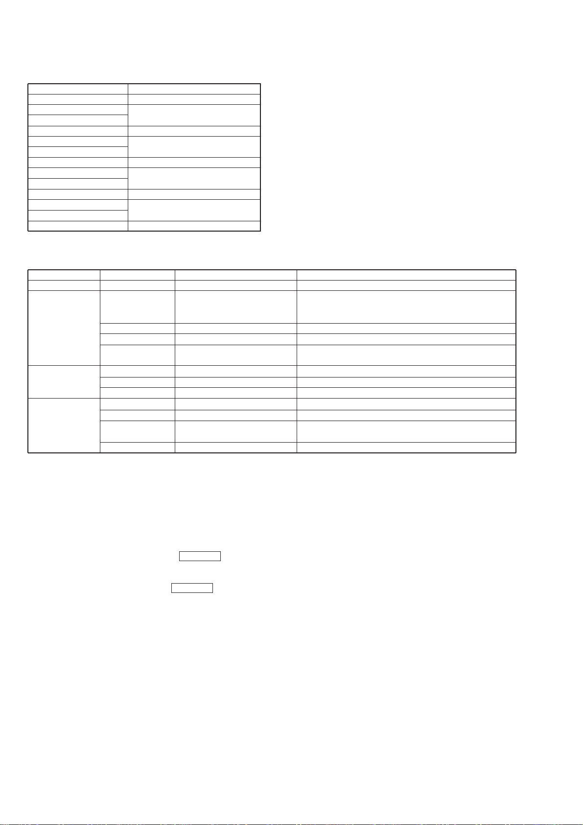
• Description of History Codes
History code number Description
1st 0 The first error
1st 1
1st 2
N 0 The last error
N1
N2
N-1 0 One error before the last.
N-1 1
N-1 2
N-2 0 Two errors before the last.
N-2 1
N-2 2
R Total recording time *1)
• Description of Error Indication Codes
Problem Indication code Meaning of code Description
No error 00
Abnormal stop
during recording
Abnormal stop
during playback
Abnormal stop of
recording/playback
caused by power
system
00 indicated
00 indicated
00 indicated
00 indicated
01 Servo error Focus out of alignment.
02 ADIP read error Unable to read the ADIP address.
03 Shock detected during write Jumped by 1.5 tracks or more due to shock during write.
04
11 No focus applied Focus could not be applied.
12 CRC error Unable to read the address.
15 FG error Abnormal rotation of disc.
21 Lower voltage due to overload P ower voltage reduced due to overload.
22 Momentary interruption Momentary interruption detected.
23
24 Low power voltage in DSP
Shock detected during
laser down
Lower power voltage in motor Power voltage for motor continuously reduced to less than
system 1V.
*1) Total recording time
Total recording time is recorded in minutes as an index for load to
the OP. It is recorded in hexadecimal format and up to 65,535 min.
(about 886 discs of 74-minute disc) can be counted. It returns to
“0000h” when recorder goes beyond this limit.
Example :REC 000A n Approx. 10 min.
REC 00A0 n Approx. 160 min.
REC 0A00 n Approx. 2,560 min.
Abnormal disc RPM.
Attempt to access an abnormal address.
Shock detected when laser was moving down.
2-6. CLEARING THE ERROR INDICATION CODE
AND TO TAL RECORDING TIME
After repair, reset the error indication code.
Reset the total recording time when you have replaced the OP.
1. Go into the self-diagnostic mode. (See page 5.)
2. To reset the error indication code, slide REC c key when
the code is displayed.
(All data including 1st, N , N-1 and N-2 are reset.)
3. T o reset the total recording time, slide REC c key when the
time is displayed.
– 6 –
Page 7
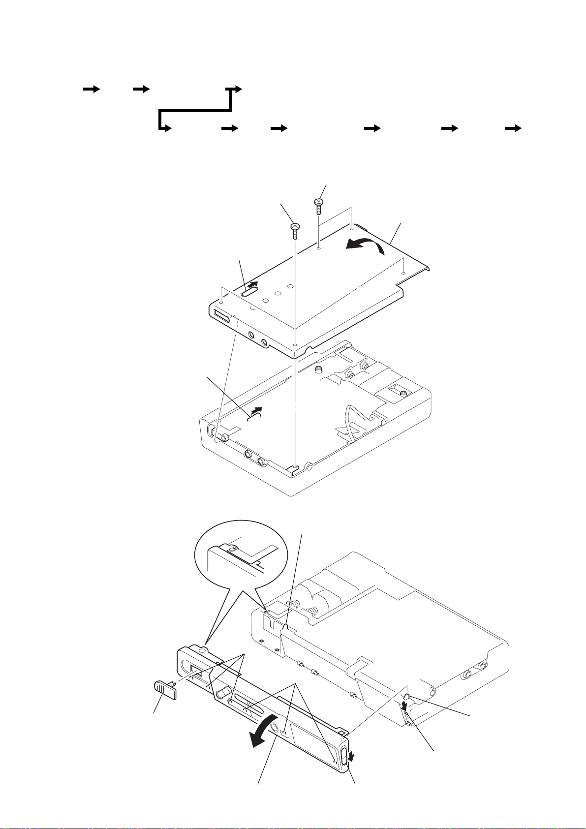
SECTION 3
y
y
y
1
1.7x4.5, tapping
2
1.7x4.5, tapping
3
panel, bottom
knob
switch
DISASSEMBLY
Note : This set can be disassemble according to the following sequence.
Set Panel,
Bottom
Panel (SV) Assy,
Front
LCD Module
Connector Main
Board
Panel (SV) Assy,
Upper
Note : Follow the disassembly procedure in the n umerical order given.
3-1. PANEL, BOTTOM
Cabinet (SV)
Ass
OP Block
Ass
Holder
Ass
3-2. PANEL (SV) ASSY, FRONT
1
knob (OPEN)
claws
4
2
claw
claws
5
panel (SV) assy, front
knob
switch
3
claw
– 7 –
Page 8
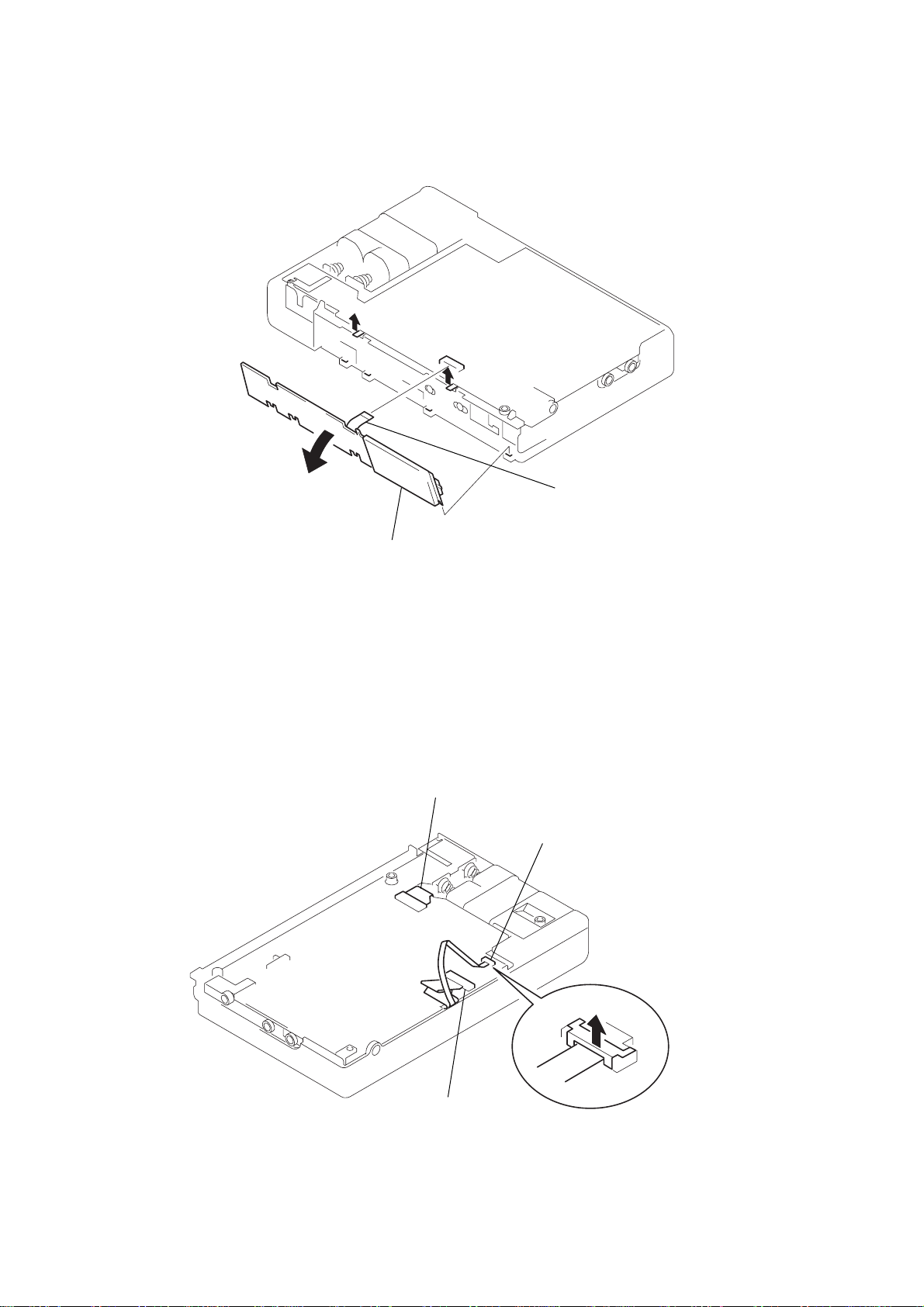
3-3. LCD MODULE
2
3
3-4. CONNECTOR
4
5
LCD module
1
CN601
2
CN702
1
CN801
– 8 –
3
CN701
Page 9
3-5. MAIN BOARD
)
2
1.7x4.5, tapping
1
1.7x4.5, tapping
4
MAIN board
3
claws
3-6. PANEL (SV) ASSY, UPPER
1
M1.4, precision
4
claw
8
panel (SV) assy, upper
7
3
bearing (stopper
6
boss
2
– 9 –
5
claw
Page 10
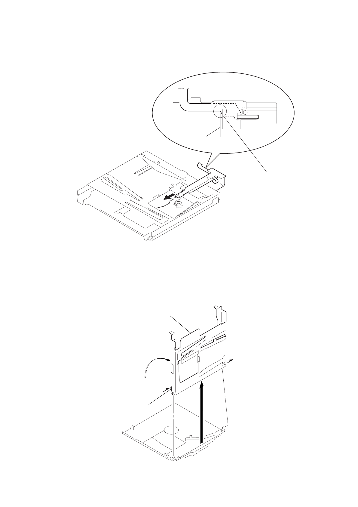
3-7. CABINET (SV) ASSY
y
n
2
MD, step
1
MD, step
4
3
mechanism block assy
cabinet (SV) ass
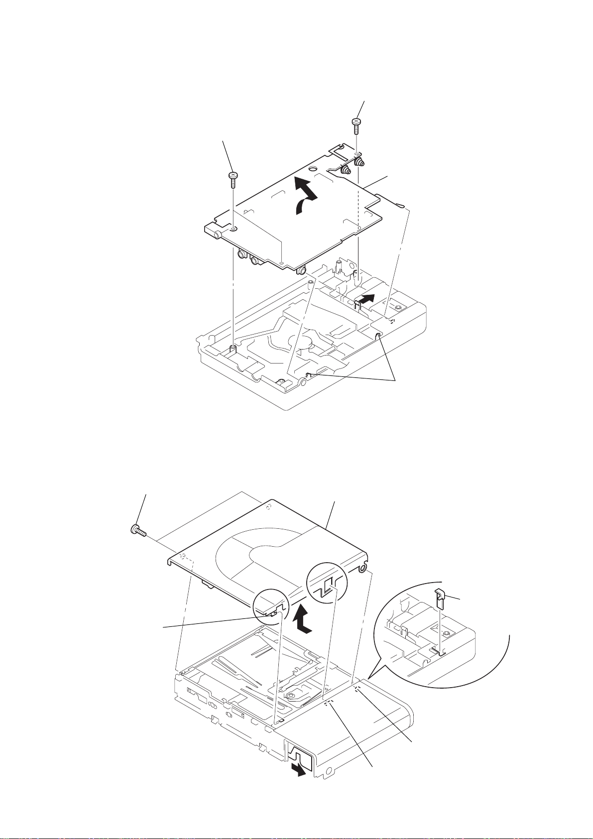
3-8. OP BLOCK ASSY
2
M1.4x3.0
adhesive sheet
1
M1.4x3.0 locking
4
flexible board
3
shaft, mai
OP block assy
– 10 –
Page 11
• Notes for Installation of the OP Block Assy
• Be careful to avoid contact
of the lens with the chassis
when installing the OP block
assy.
• Location of the Flexible Board
marked line
Align this portion of the
flexible board with the
marked line on the holder.
3-9. HOLDER ASSY
1
claw
2
4
holder assy
3
– 11 –
Page 12
SECTION 4
)
)
)
TEST MODE
4-1. GENERAL
This set provides the Overall adjustment mode (Assy mode) that
allows CD and MO disk to be automatically adjusted when in the
test mode. In this Assy mode, the system discriminates between
CD and MO disk and then automatically perform adjustments for
them in sequence. If a fault is found, the system displays its location. Also, the Serv o mode allows each indi vidual adjustment to be
automatically adjusted.
4-2. TEST MODE SETTING
See page 5.
4-3. TEST MODE STRUCTURE
Test mode
or VOLUME key
+
+
Manual Mode
VOLUME key
+
Servo Mode
Audio Mode
Mechanism Mode
Power Mode
or VOLUME key
=
–
Overall Adjustment Mode
(Assy Mode)
MODE key
Hybrid Mode (ALL Mode)
EDIT/ENTER key
Key Check Mode
4-4. MANUAL MODE
(1) Servo Mode
• How to Transfer in the Servo Mode:
Mode No. Test Description Check Write
000 Servo mode
010 Offset correction value indication
011 VC offset correction
012 Focus bias correction
013 FE offset correction
014 ABCD offset correction
015 All servo ON
016 Temperature indication
020 Laser power adjustment
021 Laser CD/MO read adjustment ® (08)
022 Laser MO write adjustment ® (4C)
023 Sled normal ® (45)
024 Sled intermittent ® (65)
025 Sled access ® (30)
030 MO test adjustment
031 MO focus search adjustment
032 MO read EF balance adjustment ® (0F)
033 MO read ABCD level ® (07)
034 MO write EF balance adjustment ® (10)
035 MO write ABCD level ® (18)
036 Laser MO read adjustment ® (08)
037 MO focus gain ® (30)
038 MO tracking gain ® (30)
039 MO focus bias ®® (0B)
040 Low reflection CD test adjustment
041
Low reflection CD focus search adjustment
042
Low reflection CD EF balance adjustment
043 Low reflection CD ABCD level ® (06)
044 Laser low reflection CD read ® (08)
045 Low reflection CD focus gain ® (30)
046 Low reflection CD tracking gain ® (30)
® (10)
Mode No. Test Description Check Write
047 Low reflection CD focus bias ®® (00)
050 CD test adjustment
051 CD focus search adjustment
052 CD EF balance adjustment ® (10)
053 CD ABCD level adjustment ® (15)
054 Laser CD read ® (08)
055 CD focus gain ® (30)
056 CD tracking gain ® (30)
057 CD focus bias ®® (00)
060 Recording test
061 32 cluster full recording
062 Recording shock
063 32 cluster full playback
Check : Mode to display error rate and cluster.
Write : Mode to permit adjustment (Default value given in paren
theses).
1. Go into the test mode.
2. Press + or VOLUME + key to set the servo mode.
Unit LCD display
XX XX SERVO
Adjustment value
(The data can be changed/written when flashing.
Mode No.
(The lower two digits are indicated.
Three digits are indicated on the
remote controller LCD.)
3. Press the keys below to change the mode No.
( : Increases the one place.
p : Sets the one place to 0.
This key brings the ten place to 0 if the one place is
0.
VOLUME + :Increases the ten place by 10 if the one place is 0.
Increases the adjustment value if the one place
is non-zero.
VOLUME – : Decreases the ten place by 10 if the one place is 0.
Decreases the adjustment value if the one place is
non-zero.
Note) Press the REC c key is the mode “33” to shift to the
mode “34”.
Press the ( key is the mode “34” to shift to the mode
“35”.
• How to Adjust in Servo Mode:
1. When the servo mode is set to the appropriate mode for each
adjustment, the lower two digits of the mode No. and the value
stored in EEPROM are displayed and flashing.
XX XX SERVO
Adjustment value (flashing
Mode No. (lower two digits
– 12 –
Page 13
2. To perform automatic adjustment for an adjustment item with
)
)
the mode number 030 to 047, press P key.
If the result of adjustment is OK, the adjustment value changes
from flashing to steady on and it is automatically written to
EEPROM.
32 OF SERVO
Adjustment value
(flashing to steady on
3. To perform manual adjustment, change the adjustment v alue with
VOLUME + or – key, and press P key to write it to
EEPROM.
Note) Normally, automatic adjustment should be performed. Do
not execute manual adjustment.
• System Gain Mode
1. This mode allows the system gain to be freely adjusted. Press
DISPLAY key to enter this mode.
32 OF S-GAIN
Adjustment value (flashing
2. Increase or decrease the adjustment value with V OLUME + or
– key.
3. Press DISPLAY or p key to return to the normal mode.
4. For the error rate display enabled:
Normal Mode
AT error rate
Press DISPLAY key
Block error rate
System gain Mode
Indicate of AT error rate
39 OA 000a4F
Cluster value
39 OA 000b4F
ATT error value
Block error value
(2) Audio Mode
• How to Transfer in the Audio Mode
Mode No. Test Description Write
100 Audio mode
110 Audio playback
111 L/R=1 kHz 0 dB Playback VOL HP output
112 L=1 kHz 0 dB Playback VOL HP output
113 R=1 kHz 0 dB Playback VOL HP output
114 L/R – ∞ dB Playback VOL HP output
115
116
117 INFI ZERO & BEEP Playback VOL HP output
120 Audio recording test
121 LINE manual recording
122
123 LINE automatic recording
124
130 DIGITAL A GC ADJ1
131 MIC UP SR ® (30)
132 MIC DOWN SR ® (FA)
133 MIC THD0 ® (D0)
134 MIC GAIN ® (00)
135 MIC A TT A CK ® (A0)
136 MIC RECOVER ® (F8)
137 MIC THD2 ® (F0)
138 MIC GAIN2 ® (D0)
139 MIC RTIME ® (01)
140 DIGITAL A GC ADJ2
141 LINE UP SR ® (17)
142 LINE DOWN SR ® (FF)
143 LINE THD0 ® (D0)
144 LINE GAIN ® (0C)
145 LINE A TTACK ® (33)
146 LINE RECOVER ® (FB)
147 LINE THD2 ® (E4)
148 LINE GAIN2 ® (5F)
149 LINE RTIME ® (04)
150 DIGITAL A GC ADJ3
151 MAN UP SR ® (C0)
152 MAN DOWN SR ® (40)
153 AUTO THD3 ® (51)
154 AUTO LMT UP SR ® (FF)
155 AUTO LMT DOWN SR ® (E0)
156 MAN THD3 ® (51)
157 MANU LMT UP SR ® (FF)
158 MANU LMT DOWN SR ® (A0)
159 THD1 ® (1A)
L/R=1 kHz 0 dB & EVR max
L/R=1 kHz 0 dB & AVLS on
*1) MIC manual recording
DEMP LINE manual recording
*1) DEMP MIC manual recording
*1) OPT automatic recording HP VOL HP output
MIC automatic recording
DEMP LINE automatic recording
*1)
DEMP OPT automatic recording
DEMP MIC automatic recording
Playback VOL HP output
Playback VOL HP output
Recording VOL HP output
Recording VOL HP output
HP VOL HP output
Change
Description
*1) The port is detected and the input is automatically selected.
Contents changed : Contents to be changed when VOLUME
+ or – key is pressed.
Write : Mode to permit adjustment
(Default value given in parentheses)
Adjustment value (flashing)
Mode No. (lower two digits)
Indicate of block error rate
Note) In normal service, do not adjust the system gain mode.
1. Go into the test mode.
2. Press + key or VOLUME + key and VOLUME + key in
this turn to set the audio mode.
– 13 –
Page 14
Unit LCD display (3) Mechanism Mode
)
)
• How to Transfer the Mode in the Mechanism Mode:
Mode No. Test Description Operation
200 FUNCTION Stepper control
XX XX AUDIO
Adjustment value
(The data can be changed/written when flashing.
Mode No.
(Lower two digits are displayed.)
3. Press the keys below to change the mode number.
( : Increases the one place.
p : Sets the one place to 0.
This key brings the ten place to 0 if the one place
is 0.
VOLUME + : Increases the ten place by 10 if the one place is 0.
Increases the adjustment value if the one place is
non-zero.
VOLUME – : Decreases the ten place by 10 if the one place is 0.
Decreases the adjustment value if the one place is
non-zero.
• How to Adjust in the Audio Mode
1. When the audio mode is set to the appropriate mode for each
adjustment, the lower tow digits of the mode No. and the value
stored in EEPROM are displayed and flashing.
2. Change the adjustment value with VOLUME + or – key and
press P key to write the new value to EEPROM.
• How to Check in the Audio Mode
The audio mode allows the checks below to be performed:
1. For the mode numbers of 111 to 113, 115 and 116, pressing P
key will activ ate a beep. But for the mode number of 117, pressing P key will not activate a beep. (No beep sounds when
c HOLD switch is put on.)
2. For the mode numbers of 121 to 124, pressing Digital MEGA
BASS key will display the DBB mode for the adjustment v alue.
1 : Mode 1
2 : Mode 2
13 : OFF
(This will not be accepted when the LINE OUT jack is plugged.
The display will be 13 : OFF when LINE OUT jack is plugged
in Modes 1 and 2.)
210 MECHA test Initial position return
211 HEAD adjustment Operation variation changing (19)
212 REC position Recording head descent
220 RESUME Resume
221 RESUME CLEAR Resume clear/initialization
1. Go into the test mode.
2. Press + or V OLUME + and V OLUME + and V OLUME
+ in this turn to set the mechanism mode.
Unit LCD display
XX XX MECHA
3. Press the keys below to change the mode No.
( : Increases the one place.
p : Sets the one place to 0.
This key brings the ten place to 0 if the one place is
0.
VOLUME + : Increases the ten place by 10 if the one place is 0.
Increases the adjustment value if the one place
is non-zero.
VOLUME – : Decreases the ten place by 10 if the one place is 0.
Decreases the adjustment value if the one place is
non-zero.
• How to Check in the Mechanism Mode
The mechanism mode allows the checks below to be performed:
1. For the mode numbers of 200, 210 to 212, 220 and 221, pressing
= key will move the optical pickup to the inner radius.
Pressing + key will move the pickup to the outer radius.
2. For the mode numbers of 211 and 212, pressing P key will
start aging. Pressing p key will stop aging.
• Mode No. 211 ... Sled aging with stepper at playback position.
• Mode No. 212 ... Sled aging with stepper at recording position.
3. With the mode number 210 selected, pr essing P k ey will start
aging with steeper at between home and recording positions.
p key will stop aging.
( ) : Default value
Adjustment value
Mode No.
(Lower two digits are displayed.
– 14 –
Page 15
)
)
(4) Power Mode
Mode No. Test Description Indication value Remark
300 POWER test
310 POWER SUPPLY
311 DC IN +B voltage value
320 CHG TEST
321 Charging start
322 BA TT under CHGMNT
voltage value
323 BATT under +B CHGMNT
voltage value
4-5. O VERALL ADJUSTMENT MODE (ASSY MODE)
• How to Adjust in Assy Mode
1. Go into the test mode.
2. Press = or VOLUME – key.
XX ASSY-M
1. Go into the test mode.
2. Press + key or VOLUME + and VOLUME + and VOLUME + and VOLUME + in this turn to set the power mode.
XX XX POWER
Adjustment value
Mode No.
(Lower two digits are displayed.
3. Press the keys below to change the mode No.
( :Increases the one place.
p : Sets the one place to 0.
This key brings the ten place to 0 if the one place is
0.
VOLUME + : Increases the ten place by 10 if the one place is 0.
Increases the adjustment value if the one place
is non-zero.
VOLUME – : Decreases the ten place by 10 if the one place is 0.
Decreases the adjustment value if the one place is
non-zero.
Note) With the mode number 310 selected, pressing ( key will
transfer to the mode number (311) for the currently operating power.
With the mode number 300 selected, pressing P key will
set the sleep mode. Pressing p key will release it.
3. Insert the test CD (TDYS-1) or an available SONY CD.
4. Press ( key . The system discr iminates between CD and MO
and performs automatic adjustment for CD.
51 CD-RUN
Mode No. under adjustment.
• CD Automatic Adjustment
Mode No. Adjustment Description
052 CD EF balance adjustment
053 CD ABCD level adjustment
055 CD focus gain
056 CD tracking gain
057 CD focus bias
5. If the result of automatic adjustment is OK, the following display appears:
CD-OK
MD-OK
(CD)
(MD)
• How to Check in the Power Mode
1. For the mode numbers of 311, the voltage of the currently
operating power is displayed.
6. If the result of automatic adjustment is NG, the following display appears:
XX XX CD-NG
Result of adjustment
NG mode No. (lower two digits
XX XX MD-OK
– 15 –
Page 16
* For the mode numbers of 039 and 057, if the focus bias value is
)
00
)
NG, the following display is repeated:
55 30
Focus bias value
Mode No.
While P key is being depressed
10. If the result of automatic adjustment is OK, the following display appears:
11. If the result of automatic adjustment is NG, the following display appears:
82 00
77 01
Error code (01 to 04)
Meaning of focus bias
* For the mode numbers of 039 and 061, if the At error rate is NG,
the following display is repeated:
39 03
At error value
Mode No. (lower two digits
7. If NG, set the servo mode. Perform automatic adjustment for
the items not accepted (see the servo mode).
8. Insert a MO disk.
9. Press ( key . The system discr iminates between CD and MO
and performs automatic adjustment for the MO disk.
Result of adjustment
NG Mode No. (lower two digits
12. If NG, set the servo mode. Perform automatic adjustment for
the items not accepted (see the servo mode).
4-6. HYBRID MODE, KEY CHECK MODE
These modes are not used in normal service.
61
• MO Automatic Adjustment
Mode No. Adjustment Description
032 MO read EF balance adjustment
033 MO read ABCD level
034 MO write EF balance adjustment
035 MO write ABCD level
037 MO focus gain
038 MO tracking gain
061 32 cluster full recording
062 Recording shock
063 32 cluster full playback
039 MO focus bias
042 Low refrection CD EF balance adjustment
043 Low refrection CD ABCD level
044 Laser low reflection CD read
046 Low refrection CD tracking gain
Mode No. (lower two digits)
– 16 –
Page 17
r
e
Ver 1.4 2001. 01
SECTION 5
ELECTRICAL ADJUSTMENTS
PRECAUTIONS FOR ADJUSTMENT
1) Perform all adjustments in the order given in the test mode.
After adjusting, exit the test mode.
2) Use the following tools and measuring instruments.
• Test CD TDYS-1
(Part No. : 4-963-646-01)
• SONY MO disc available on the market
• Laser power meter LPM-8001
(Part No. : J-2501-046-A)
• Oscilloscope (Frequency band above 40 MHz. Perform the
calibration of probe first before measuring.)
• Digital voltmeter
3) Unless specified othewise, supply DC 4.5V from the DC IN 4.5V
jack.
4) Swtich, knob positions
HOLD switch .............. OFF
AVLS switch ................ NORM
LASER POWER CHECK
Connection :
laser
power meter
Optical pick-up
objective lens
MO TRA VERSE ADJUSTMENT
Connection :
oscilloscop
MAIN board
SP526 (TE)
AP503 (VC)
Adjustment Method :
1. Set the servo mode of the test mode (Mode : 000).
2. Press the ( key , and set the MO test adjustment mode (Mode
: 030) using the VOLUME + or – key .
3. Press the = or + key and move the optical pick-up to
the center circumference.
4. Insert any MO disk available on the market.
5. When the ( key is pressed, the MO read EF balance adjustment mode (Mode : 032) will be set after MO focus search
adjustment mode (Mode : 031).
6. Press the P key to perform automatic adjustment, and check
that the traverse waveform is symmetrical at the top and bottom.
7. Slide the REC key and set the MO write EF balance adjust
ment mode (Mode : 034).
8. Press the P key to perform automatic adjustment, and check
that the traverse waveform is symmetrical at the top and bottom.
(Traverse waveform)
digital voltmete
MAIN board
AP5117 (VCC)
AP574 (LDI0)
Adjustment Method :
1. Set the servo mode of the test mode (Mode : 000).
2. Press the ( key, and set the laser power adjustment mode
(Mode : 020) using the VOLUME + or – key .
3. Press the = key and move the optical pick-up to the inner
most circumference.
4. Open the cover and set the laser power meter on the objective
lens of the optical pick-up.
5. Press the ( key, and set the laser CD/MO read adjustment
mode (Mode : 021).
6. Check that the laser power meter reading is 0.85 ± 0.085 mW.
7. Check that the voltage between AP5117 (VCC) and AP574
(LDI0) at this time is below 40 mV.
8. Press the ( key, and set the laser MO write adjustment
mode (Mode : 022).
9. Check that the laser power meter reading is 6.8 ± 0.68 mW.
10. Press the P key to finalize the adjustment data.
11. Check that the voltage between AP5117 (VCC) and AP574
(LDI0) at this time is below 80 mV.
12. Press the p key.
13. Exit the test mode.
A
0 V
B
Specification : A = B, C 1.0 Vp-p
>
=
9. Check that the traverse level at this time is above 1.0 Vp-p.
10. Press the p key.
11. Exit the test mode.
Note) Using a recorded disk in this adjustment will erase the data.
Adjustment Location : See page 19.
C
Adjustment Location : See page 19.
– 17 –
Page 18

LOW REFLECTION CD TRAVERSE ADJUSTMENT
e
e
Connection :
CD TRA VERSE ADJUSTMENT
Connection :
oscilloscop
MAIN board
SP526 (TE)
AP503 (VC)
Adjustment Method :
1. Set the servo mode of the test mode (Mode : 000).
2. Press the ( key , and set the low reflection CD test adjustment
mode (Mode : 040) using the VOLUME + or – key.
3. Insert any MO disk available on the market.
4. When the ( key is pressed, the low reflection CD EF balance
adjustment mode (Mode : 042) will be set after low reflection
CD focus search adjustment mode (Mode : 041).
5. Press the P key to perform automatic adjustment, and check
that the traverse wa veform is symmetrical at the top and bottom.
(Traverse waveform)
A
0 V
B
Specification : A = B, C 0.9 Vp-p
>
=
6. Check that the traverse level at this time is above 0.9 Vp-p.
7. Press the p key.
8. Exit the test mode.
Adjustment Location : See page 19.
oscilloscop
MAIN board
SP526 (TE)
AP503 (VC)
Adjustment Method :
1. Set the servo mode of the test mode (Mode : 000).
2. Press the ( key, and set the CD test adjustment mode (Mode
: 050) using the VOLUME + or – key.
3. Press the = or + key and move the optical pick-up to the
center circumference.
4. Insert a test CD (TDYS-1).
5. When the ( key is pressed, the CD EF balance adjustment
mode (Mode : 052) will be set after CD focus search adjustment
mode (Mode : 051).
6. Press the P key to perform automatic adjustment, and check
that the traverse wav eform is symmetrical at the top and bottom.
(Traverse waveform)
C
0 V
Specification : A = B, C 1.0 Vp-p
>
=
7. Check that the traverse level at this time is above 1.0 Vp-p.
8. Press the p key.
9. Exit the test mode.
A
C
B
Adjustment Location : See page 19.
– 18 –
Page 19

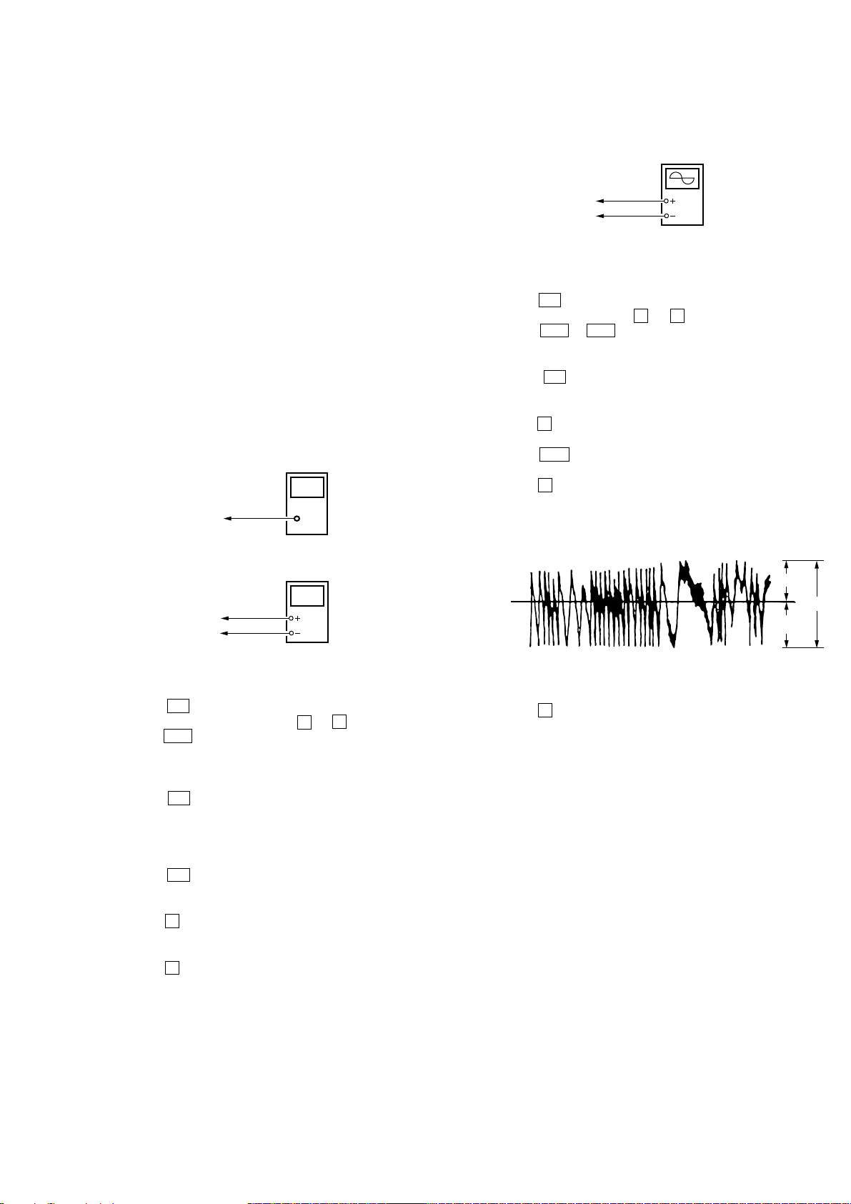
CD RF LEVEL CHECK
r
AP538 (RF)
IC701
CN501
IC501
IC901
AP574 (LDIO)
AP503 (VC)
AP5117 (VCC)
MAIN BOARD (SIDE B)
MAIN BOARD (SIDE A)
SP526 (TE)
Connection :
oscilloscope
MAIN board
AP538 (RF)
AP503 (VC)
digital voltmete
Adjustment Method :
1. Set the servo mode of the test mode (Mode : 000).
2. Press the ( key, and set the CD test adjustment mode
(Mode : 050) using the VOLUME + or – key.
3. Press the = or + key and move the optical pick-up to
the center circumference.
4. Insert a test CD (TDYS-1).
5. When the ( key is pressed, the CD EF balance adjustment
mode (Mode : 052) will be set after CD focus search adjustment mode (Mode : 051).
6. When the ( key is pressed, the CD ABCD level adjustment
mode (Mode : 053) is set.
7. Press the P key to perform automatic adjustment, and check
that the RF level is 1.1 ± 0.33 Vp-p.
MAIN board
AP5117 (VCC)
AP574 (LDIO)
Adjustment Location :
(RF waveform)
8. Check that the voltage between AP5117 (VCC) and AP574
(LDIO) and at this time is below 40 mV.
9. Press the p key.
10. Exit the test mode.
1.1 ± 0.33 Vp-p
– 19 –
Page 20

SECTION 6
DIAGRAMS
6-1. IC PIN DESCRIPTIONS
• IC601 CXD2652AR (DIGITAL SERVO, ENC/DEC & ATRAC MEMORY CONTROLLER)
Pin No. Pin name I/O Pin Description
1 MNT 0 O Traverse count signal output.
2 MNT 1 O Track jump detect output.
3 MNT 2 — Not used (Open).
4 MNT 3 O Focus OK signal output.
5 SWDT I Inputs write data signal from system control (IC801).
6 SCLK I Inputs serial clock signal from system control (IC801).
7 XLAT I Inputs serial latch signal from system control (IC801).
8 SRDT O Outputs write data signal to system control (IC801).
9 SENS O Outputs internal status (SENS) to system control (IC801).
10 XRST I Inputs reset signal from system control (IC801). L : Reset
11 SQSY O
12 DQSY O
13 WRPWR I Inputs laser power switching signal from system control (IC801).
14 NC — Not used (Open).
15 TX I
16 OSC1 O Clock output (22.5 MHz).
17 OSC0 I Clock input (22.5 MHz).
18 XTSL — Not used (Fixed at “L”)
19 NC — Not used (Connect to ground).
20 RVSS — Connect to ground.
21 DIN I Digital audio signal input pin (For optical input).
22 NC — Not used (Open).
23 ADDT I Audio data input from A/D converter (IC301).
24 DATA O Monitor/decode audio data output to A/D converter (IC301).
25 ALRCK O L/R clock output to D/A converter (IC301).
26 ABCK O Bit clock signal output to A/D, D/A converter (IC301).
27 FS256 O 11.2896 MHz clock output (MCLK).
28 DVDD — Power supply (+2.8 V) for digital.
29 – 39 A00 – A08, A10, A11 O Address signal output to DRAM (IC602).
40 DVSS — Ground terminal.
41 XOE O Output enable contol signal output to DRAM (IC602).
42 XCAS O Column address strobe singal output to DRAM (IC602).
43 A09 O Address signal output to DRAM (IC602).
44 XRAS O Row address strobe signal output to DRAM (IC602).
45 XWE O Read/write control signal output to DRAM (IC602).
46 – 49 D0 – D3 I Data signal input from DRAM (IC602).
50 MVCI — Not used (Connect to ground).
51 ASYO O Playback EFM full-swing output (L : VSS, H : VDD).
52 ASYI I Playback EFM asymmetry comparate voltage input.
53 AVDD — Power supply (+2.8 V) for analog.
54 BIAS I Playback EFM asymmetry circuit constant current input.
55 RFI I Inputs playback EFM RF signal from RF amplifier (IC501).
Output subcode Q sync (SCOR) to system control (IC801).
Outputs “L” every 13.3 msec. Outputs “H” at all most mostly.
Outputs digital-in U-bit CD format subcode Q sync (SCOR) to system control (IC801).
Outputs “L” every 13.3 msec. Outputs “H” at all most mostly.
Input of write data taransmission timing from system control (IC801).
Also used as magnetic field head ON/OFF output.
– 20 –
Page 21

Pin No. Pin name I/O Pin Description
56 AVSS — Ground terminal.
57 PDO — Not used (Open).
58 PCO O Decoder PLL master clock PLL phase comparison output.
59 FILI I Decoder PLL master clock PLL filter input.
60 FILO O Decoder PLL master clock PLL filter output.
61 CLTV I Decoder PLL master clock PLL VCO control voltage input.
62 PEAK I Inputs peak hold signal for light amount signal from RF amplifier (IC501).
63 BOTM I Inputs bottom hold signal for light amount signal from RF amplifier (IC501).
64 ABCD I Light amount signal from RF amplifier (IC501).
65 FE I Input focus error signal from RF amplifier (IC501).
66 AUX1 I Input of auxiliary signal from RF amplifier (IC501).
67 VC I Input of middle point voltage (+1.4 V) from RF amplifier (IC501).
68 ADIO — Not used (Open).
69 AVDD — Power supply (+2.8 V) for analog.
70 ADRT — Not used (Connect to +2.8 V).
71 ADRB — Not used (Connect to ground).
72 AVSS — Ground terminal.
73 SE I Input of sled error signal from RF amplifier (IC501).
74 TE I Input of tracking error signal from RF amplifier (IC501).
75 AUX2 — Not used (Connect to +2.8 V).
76 DCHG — Not used (Connect to +2.8 V).
77 APC — Not used (Connect to +2.8 V).
78 ADFG I
79 FO CONT O Focus control output to RF amplifier (IC501).
80 XLRF I Latch signal input from RF amplifier (IC501).
81 CKRF O RFCK clock (7.35 kHz) signal output.
82 DTRF I Serial data input from RF amplifier (IC501).
83 APCREF I Laser power setting signal input.
84 LDDR — Not used (Open).
85 TRDR O Tracking servo drive signal output (–).
86 TFDR O Tracking servo drive signal output (+).
87 DVDD — Power supply (+2.8 V) for digital.
88 FFDR O Focus servo drive signal output (+).
89 FRDR O Focus servo drive signal output (–).
90 FS4 O 176.4 kHz clock signal output (MCLK).
91 SRDR O Sled servo drive signal output (–).
92 SFDR O Sled servo drive signal output (+).
93 SPRD O Spindle servo drive signal output (–).
94 SPFD O Spindle servo drive signal output (+).
95 FGIN I FG signal input from spindle motor driver (IC761).
96 TEST1 — Not used (Connect to ground).
97 TEST2 — Not used (Connect to ground).
98 TEST3 — Not used (Connect to ground).
99 DVSS — Ground terminal.
100 EFMO O EFM recording signal output.
Input of ADIP dual FM signal from RF amplifier (IC501) (22.05 kHz ± 1 kHz).
(TTL Schmit input)
– 21 –
Page 22

• IC801 CXP740010 (SYSTEM CONTROL)
Pin No. Pin name I/O Pin Description
1 CLKCS O Not used (Chip select output to real time clock).
2 XRST O Reset output. L : Reset
3 WRPWR O Laser power switching signal output.
4 TX O Write data transfer timing output.
5 SDI2 I Serial data input.
6 SDO2 O Serial data output.
7 SCK2 O Serial clock output.
8 RFSW O Power control output.
9 SSB I/O SSB data signal input and output.
10 SSB SCK I/O SSB clock signal input and output. (Not used (Open).)
11 DTCK I/O Remote control data signal input/output.
12 SPCK — Not used (Open).
13 WP I Wake-up signal input from remote control key and this unit key.
14 OPEN I Detecting switch for opening and closing of the upper cover. L : Close
15 CLOCK I Not used (CLOCK SET switch input).
16 NI MH CHG O NI MH charge control output.
17 SLEEP O Sleep signal output.
18 T.MARK I T.MARK (Track mark) switch input.
19 REC I Not used (REC switch input).
20 PROTECT I Disc write protect switch. H : Protect
21 HOLD I HOLD switch input (This unit). L : HOLD
22 SYNC REC I SYNCHRO REC switch input.
23 D. B. B I DIGITAL MEGA BASS slide switch input.
24 XLINEDET I LINE IN (OPTICAL) detection input. L : LINE IN
25 INMU1 O INMU signal output.
26 XTEST I Test mode terminal. L : Test mode
27 XDCIN I Not used (Open). (DC input detect. L : DC IN)
28 KANA SE L — Not used (Open).
29 XPHOTO SW O ON/OFF control signal output of PHOTO circuit.
30 XP CONT — Not used (Open). (Power control output. L : ON)
31 X2VCONT —
32 XREC LED — Not used (Open). (REC LED control. L : ON)
33 MODE2 O
34 MODE1 O
35 XNIMH CHG — Not used (Open). (Battery charger control signal output. L : Charge)
36 XLCD ON O LCD ON/OFF control. L : ON
37 INMU0 O INMU signal output.
38 MRST I Microprocessor reset input.
39 VSS — Ground.
40 XTAL — System clock (12 MHz).
41 EXTAL — System clock (12 MHz).
42 LCD DS O LCD communication strobe signal output to LCD driver.
43 LCD XC D O Com/data select signal output.
44 LCD DATA O LCD data output.
45 LCD SCK O Serial clock output.
46 CHG MNT I Battery charge voltage minitor input.
47 INLS I Detecting switch for internal circuit of sleding. L : Internal circuit
48 HIDC MNT I Voltage monitor DC input.
49 KEY R I Remote control key input.
Not used (Open). (Outputs H while operating with a lithium battery. 2V power control
signal output. L : ON)
REC drive (IC901) control signal output.
– 22 –
Page 23

Pin No. Pin name I/O Pin Description
50 AVSS — Ground terminal for A/D converter.
51 AVREF I A/D converter reference voltage input.
52 AVDD — A/D converter power supply terminal.
53 VLG2-MNT I DSP power monitor signal.
54 TEMP I Temp meter (IC802) input.
55 KEY3 I Key input.
56 KEY2 I Key input.
57 KEY1 I Key input.
58 XINT REC SW I Recording head position detect input.
59 UNREG MNT I 2.8 V voltage monitor input.
60 BAT VC I Battery detect signal input.
61 FG IN I FG input from motor driver (IC503).
62 NC — Not used (Open).
63 FOK PORT I Focus OK signal input.
64 –––– — Not used (Open).
65 LCD RESET O LCD reset signal output.
66 XJACKDET I LINE IN (OPTICAL) jack detection input.
67 OPT DET I LINE IN (OPTICAL) optical detection input.
68 XMIC DET I MIC (PLUG IN) jack detection.
69 (NC) — Not used (Open).
70 FSI (NC) — Not used (Open).
71 SPOFF O
72 RSI O
73 RH PWM O RH constant current control signal output.
74 (NC) — Not used (Open).
75 DQSY I Subcode Q sync (SCOR) of digital in U-bit CD format from IC601.
76 T COUNT I Traverse count signal input.
77 SDI1 I Serial data input.
78 SDO1 O Serial data output.
79 SCK1 O Serial clock output.
80 SQSY I SUB-Q/ADIP SYNC input.
81 BEEP O BEEP sound output control.
82 XLAT O Latch output.
83 NC — Not used (Open).
84 TEX — Not used (Fixed at “L”).
85 TX — Not used (Fixed at “L”).
86 VSS — Ground.
87 VDD — Power supply pin (+2.8V).
88 NC — Not used (Fixed at “H”).
89 XCS ADA O A/D, D/A converter chip select output.
90 XPD ADA O A/D, D/A converter power down signal output. H : Power down
91 KEY ON O SLEEP : L, action : H.
92 XNIMH DET (NC) — Not used (Open). (Battery detect switch input.)
93 A MUTE O Analog mute control. H : Mute
94 XOPT CTL O Power supply control output for an optical input.
95 FFCLR O Flip flop clear signal output.
96 XCE NV O EEPROM chip select output.
97 SENS I SENS input.
98 LDON O “H” : APC circuit ON, “L” : APC circuit OFF
99 XSHOCK I Track jump detection input from IC601.
100 CLV STB O CLV drive control signal output.
REC head motor control signal output.
– 23 – – 24 –
Page 24

MZ-R37
6-2. BLOCK DIAGRAM — SERVO SECTION —
04
OVER
WRITE
HEAD
MOTOR
SPINDLE
MOTOR
MD MECHANISM
OPTICAL
PICK-UP
PD
VCC
TRACKING
COIL
FOCUS COIL
SLED
SD+
SD–
AOUT
AOUTB
PROTECT
XINTREC SW
INLS
COM
2.8V
REC DRIVE
IC901 (1/2)
8
MODE1
9
MODE2
12
17
14
11
63
62
RF AMP
IC501
AUX
SW
ABCD
AMP
AI
AMP
2.8V
HA
HB
TRACKING
XSTBY
POWER
SWITCH
Q761
EFM
LOGIC
AGC/
PEAK/
BOTTOM
FOCUS
ERROR
AMP
ERROR
AMP
XPHOTO SW
EFM
64
RF
RF
EQ
38
AUX
33
PEAK
37
BOTM
36
ABCD
354
FE
34
ADFG
32
TE
26
SE
28
SWDT
16
SCLK
17
XLAT
18
APCREF
12
FO CONT
20
Q581
(1/2)
FOCUS/TRACKING COIL
SLED/SPINDLE MOTOR DRIVE
IC701
29
DRIVE
27
8
DRIVE
10
12
DRIVE
14
4
DRIVE
6
DRIVE
25
2.8V
100
65
Q581
(2/2)
20
21
16
17
34
PSB
18
19
SPOFF
35
RSI
3
22 94
CLV STB
XRFSW
OVER WRITE
HEAD DRIVE
Q741,742
I
J
A
B
C
D
E
F
+
–
+
–
W
V
U
1
2
VC
3
5
6
7
8
9
10
SPINDLE MOTOR DRIVE
6
19
20
1
VCVC
AUTO POWER
CONTROL
LDON
IC761
DRIVE
RF
AMP
I-V
CONV.
I-V
CONV.
APC
Q571
11 19
VM
STBY
FG
DIGITAL SERVO ENC/DEC
ATRAC MEMORY CONTROLER
EFMO
EFM/
ACIRC
ENCODER/
DECODER
RFI
55
AUX1
66
PEAK
62
BOTM
63
ABCD
64
FE
ADFG
78
TE
74
SE
73
DTRF
82
CDRF
81
XLRF
80
APCREF
83
FO CONT
79
16
17
X601
22.5MHz
86
85
88
89
92
91
93
3 4
IC601
MEMORY
CONTROL
OSCI
OSCO
TFDR
TRDR
FFDR
FRDR
SFDR
SRDR
SPFD
SPRD
HIGH
VCC DET
IC581
&
SHOCK
PROOF
DIGITAL
AUDIO
IN
XWE
XRAS
XCAS
XOE
D0-D3
A00
A09
DADT
ADDT
ALRCK
ABCK
FS256
FS4
MNT 0
MNT 1
MNT 3
SWDT
SCLK
XLAT
SRDT
SENS
XRST
SQSY
DQSY
WRPWR
FGIN
2.8V
DIN
DRAM
IC602
45
44
42
41
46
|
49
29
|
32
•
|
34
|
38
•
43
24
23
25
26
27
3
4
17
16
1
•
2
•
18
•
19
5
|
9
•
11
|
15
XWE
XRAS
XCAS
XOE
DQ1-DQ4
A0
A9
SDTI
SDTO
LRCK
BCK
MCLK
A
AUDIO
SECTION
(Page 27)
21
DIN
XRST
SYSTEM
90
FS4
C
CONTROL
SECTION
(Page 30)
SYSTEM CONTROL
IC801 (1/3)
1
2
4
5
6
7
8
9
10
11
12
15
TX
13
95
76
T COUNT MODE 1
99
XSHOCK
63
FOK PORT
78
SDO 1
79
SCK 1
82
XLAT
77
SDI 1
97
SENSE
2
XRST
80
SQSY
DQSY
TX
WRPWR
FGIN
XPHOTOSW
XINTRECSW
75
4
3
61
MODE 2
CLV STB
RF SW
RSI
SPOFF
INLS
PROTECT
LDON
34
33
100
8
72
71
29
47
58
20
98
Signal path
: PLAY(DIGITAL)
: REC(DIGITAL)
R-ch : same as L-ch.
– 25 – – 26 –
Page 25

MZ-R37
6-3. BLOCK DIAGRAM — AUDIO SECTION —
DIN
SERVO
SECTION
(Page 26)
04
SDTO
A
LRCK
BCK
SDTI
MCLK
XRST
4
2
3
5
1
46
EEPROM
IC803
DO
SCK
AUDIO
CONTROL
CS
DI
I/F
1
3
4
2
Signal path
ADC
DAC
CDTI
CDTO
CCLK
15 14 13 12 47
KCS
PD
: PLAY(DIGITAL)
: REC(DIGITAL)
: PLAY(ANALOG)
: REC(ANALOG)
R-ch : same as L-ch.
RCH
RCH
90
89
7
5
6
96
A/D, D/A
CONVERTER
IC301
SYSTEM CONTROL
IC801 (2/3)
XPD ADA
XCS ADA
SCK 2
SDI2
SDO2
XCSNV
OPT CONT
XJACK DET
XMIC DET
XLINE DET
KEY RMC
SYSTEM
CONTROL
SECTION
(Page 29)
BEEP
AMUTE
OPT DET
DTCK
6-4. BLOCK DIAGRAM — SYSTEM CONTROL SECTION —
2.8V
41
44
25
26
29
81
93
94
66
67
68
24
11
49
KEYRMC
B
7 5
MIC AMP
IC302
8
MIC 2.5V
17
LINE/HP AMP
IC303
16
21
23
MUTE VCOM
9
4
6
OPT
CONTROL
Q302
REG
IC304
5
MIC2.5V 2.8V
XCE
3
INOUT
J301
LINE IN
(OPTICAL)
R-CH
2
R-CH
R-CH
RVCC
DTCK
KEY R
(+2.8V)
J303
MIC
(PLUG IN POWER)
J302
LINE OUT
J304
/REMOTE
AUDIO
SECTION
(Page 27)
KEYRMC
B
SYSTEM CONTROL
IC801 (3/3)
WP
LCD
MODULE
WITH
SWITCH
MEGA BASS
TEMP
METER
IC802
UNIT
S805
Digital
S803
T. MARK
41
VDD
(+2.9V)
X801
12MHz
S802
(OPEN 2)
S881
DISPLAY
S882
MODE
Q801(1/2)
S804
SYNCHRO
REC
OFF
ON
VCC
(+2.8V)
S801
(OPEN 1)
Q821
POWER
SWITCH
VCC
(+2.8V)
04
65
LCD RESET
45
LCD SCK
44
LCD DATA
43
LCD XC D
42 91
LCD STB KEY ON
57
KEY 1
56
KEY 2
21
HOLD
36
XLCD
41
EXTAL
40
XTAL
22
SYNC REC
23
DBB
18
T.MARK
54
TEMP
14
OPEN
55
KEY3
D801
MRST
SLEEP
INMU0
INMU1
NI MH CHG
FFCLR
WP
CHG MNT
BAT VC
HIDC MNT
38
17
Q902
WP
Q801
(2/2)
Q901
IC951
4 1
Q851
37
25
16
95
13
46
60
48
POWER CONTROL
IC901
FS4
25 67
REMKEY VC
24
KEY ON
6
72
23
10
70
69
71
52
51
XRST
SLEEP
INMU
CHG
FFCLR
WAKEO
WAKE
RS
CHG SW
VLG2
VLG20
VLG20
VB
VB
VL
VL1
VB
VB
L4
VDD
INM4
RF4
DC IN
68
14
47
48
32
33
37
38
39
40
49
61
54
55
57
FS4
VDD
(+2.9V)
+2.8V
+2.8V
D905
IC971
DC-DC CONVERTER
2 1
VOUT VIN
VCE VOUT
EXT
5
SERVO
C
SECTION
(Page 26)
Q971
IC972
REG
1 3
Q903
D902
Q906
D906
D901
T901
UNREG
RECHARGEABLE
BATTERY
(NC-AA)
700mAh 2.4V
J901
DC IN 4.5V
¥
(CHASSIS)(CHASSIS)
– 27 – – 28 – – 29 –
– 30 –
Page 26

MZ-R37
• Semiconductor
Location
Ref. No. Location
D401 E-4
D402 H-4
D403 G-3
D404 H-25
D406 C-3
D407 D-26
D408 F-26
D741 B-20
D742 C-20
D801 G-22
D901 H-17
D902 H-16
D903 H-19
D904 G-17
D905 H-19
D906 G-11
D907 H-16
6-5. PRINTED WIRING BOARD
IC301 D-24
IC302 C-25
IC303 F-24
IC304 A-23
IC501 E-19
IC601 E-21
IC602 F-23
IC701 C-19
IC761 C-21
IC801 C-22
IC802 D-4
IC803 E-5
IC901 G-20
IC951 B-22
IC971 H-17
IC972 H-11
J301 D-3
Q302 D-4
Q571 D-18
Q741 B-20
Q742 D-20
Q761 D-21
Q801 G-22
Q821 H-5
Q851 C-21
Q901 H-22
Q902 H-17
Q903 G-16
Q906 H-18
Q971 H-17
Note:
• Y : parts extracted from the conductor side.
• b : Pattern from the side which enables seeing.
(The other layer’s patter ns are not indicated.)
Caution:
Pattern face side: Parts on the pattern face side seen from the
(Side B) pattern face are indicated.
Parts face side: Parts on the parts face side seen from the
(Side A) parts face are indicated.
– 31 – – 32 – – 33 – – 34 –
Page 27

MZ-R37
6-6. SCHEMATIC DIAGRAM — MAIN SECTION (1/3) — • Refer to page 44 for IC Block Diagrams.
• Wavef orms
VOLT/DIV : 0.5V AC
1
TIME/DIV : 1µsec
IC501
VOLT/DIV : 0.1V AC
2
TIME/DIV : 0.1msec
Approx. 0.5Vp-p
IC501 @ª
VOLT/DIV : 1V AC
3
TIME/DIV : 5msec
13.4msec
IC601
VOLT/DIV : 1V AC
4
TIME/DIV : 20nsec
1.0±0.3Vp-p
#•
2.8Vp-p
!¡
(Page 42)
(Page 38)
(Page 38)
(Page 43)
(Page 42)
(Page 38)
(Page 38)
(Page 38)
2.6Vp-p
22.5MHz
IC601
!¶
Note:
• All capacitors are in µF unless otherwise noted. pF: µµF
50 WV or less are not indicated except for electrolytics
and tantalums.
• All resistors are in Ω and 1/
specified.
• % : indicates tolerance.
Note:
The components identified by mark ! or dotted
line with mark ! are critical for safety.
Replace only with part
number specified.
• A : B+ Line.
• P ower voltage is dc 4.5 V and fed with regulated dc pow er
supply from external power voltage jack.
• Voltage and waveforms are dc with respect to ground
under no-signal conditions.
no mark : PB
( ) : REC
• V oltages are taken with a VOM (Input impedance 10 MΩ).
Voltage var iations may be noted due to normal production tolerances.
• Waveforms are taken with a oscilloscope.
Voltage var iations may be noted due to normal production tolerances.
• Circled numbers refer to waveforms.
• Signal path.
J : PB (digital)
c : REC (digital)
: Impossible to measure
∗
4
W or less unless otherwise
Note:
Les composants identifiés par
une marque ! sont critiques
pour la sécurité.
Ne les remplacer que par une
piéce portant le numéro
spécifié.
– 35 – – 36 – – 37 –
Page 28

MZ-R37
• Wavef orm
5
VOLT/DIV : 1V AC
TIME/DIV : 20nsec
12kHz
IC801
$º
2.2Vp-p
6-7. SCHEMATIC DIAGRAM — MAIN SECTION (2/3) — • Refer to page 44 for IC Block Diagrams.
(Page 43)
(Page 42)
(Page 37)
(Page 37)
(Page 37)
(Page 37)
Note:
• All capacitors are in µF unless otherwise noted. pF: µµF
50 WV or less are not indicated except for electrolytics
and tantalums.
• All resistors are in Ω and 1/
specified.
• % : indicates tolerance.
¢
•
• C : panel designation.
• A : B+ Line.
• P ower voltage is dc 4.5 V and fed with regulated dc pow er
• Voltage and waveforms are dc with respect to ground
• V oltages are taken with a VOM (Input impedance 10 MΩ).
• Waveforms are taken with a oscilloscope.
• Circled numbers refer to waveforms.
• Signal path.
: internal component.
supply from external power voltage jack.
under no-signal conditions.
no mark : PB
( ) : REC
Voltage variations may be noted due to normal production tolerances.
Voltage variations may be noted due to normal production tolerances.
c : REC (digital)
: Impossible to measure
∗
4
W or less unless otherwise
(Page 43)
(Page 37)
(Page 37)
– 38 – – 39 – – 40 –
Page 29

6-8. SCHEMATIC DIAGRAM — MAIN SECTION (3/3) — • Refer to page 44 for IC Block Diagrams.
MZ-R37
(Page 37)
(Page 37)
(Page 38)
Note:
• All capacitors are in µF unless otherwise noted. pF: µµF
50 WV or less are not indicated except for electrolytics
and tantalums.
• All resistors are in Ω and 1/
specified.
• % : indicates tolerance.
• C : panel designation.
• A : B+ Line.
4
W or less unless otherwise
(Page 38)
• P ower voltage is dc 4.5 V and fed with regulated dc pow er
supply from external power voltage jack.
• Voltage is dc with respect to ground under no-signal
condition.
no mark : PB
( ) : REC
• V oltages are taken with a VOM (Input impedance 10 MΩ).
Voltage variations may be noted due to normal production tolerances.
(Page 38) (Page 37)
– 41 – – 42 – – 43 –
• Signal path.
F : PB (analog)
L : REC (analog)
J : PB (digital)
c : REC (digital)
Page 30

• IC Block Diagrams
MCLK
LRCK
BCLK
SDTO
SDTI
DIFO
DIFI
TST3
DCODE0
DCODE1
DCODE2
CS(SCK)
IC301 AK4517-VQ-L
CMODE
PD
RST
SSB
LIN1
RIN1
TST1
LIN2
RIN2
TST2
LIN3
DZF
3839404142434445 3747 46
DACDBBDPGA
ROUT1
OPGAR
RIN3
10
11
12
1
2
3
4
5
6
7
8
9
48
CLOCK
DIVIDER
AUDIO
I/F
CONTROLLER
CONTROL
REGISTER
I/F
151413 16 24232217 18 19 20 21
CDTO
DGND
CCLK(SSI)
CDTI(SSO)
VB
VA
VD
AGND
VCOM
IC303 AN7535SA-E1
MUTE TC
MUTE
VREF
BEEP IN
GAIN CONTROL
PRE GND
LINE NF1
LINE IN1
24 23
MUTE
VCC
1 7 10 122 3 54 6 8 9 11
VCC 1
22 21 20 19 18 17 16 15 14 13
VREF
RIPPLE
RIPPLE
VCC
DET.
VCC
BEEP
OUT 1
NC
VREF
GND
CENTER OUT
IN1
VREF
OUT 2
LINE OUT1
IN2
HPF
LINE VCC
ADO
LINE IN2
LINE NF2
NC
LINE OUT2
IC501 CXA2523AR
MORFO47MORFI46RFO45OPN
48
–
+
RFA1
+
IPGAL
36
1I
ADCL
35
VCMC
34
VCMR
33
ADCR
32
IPGAR
31
VRAD
30
LOUT2
29
ROUT2
28
VRDA
27
OPGAL
26
LOUT1
25
2J
CVB
3VC
4A
IVR
5B
IVR
6C
IVR
7D
IVR
8E
IVR
9F
IVR
GSW
10PD
11APC
12APCREF
+
–
–
RFA2
–
–
–
–
–
GND
AA
BB
CC
DD
+
14
–
–
EE
FF
TEMPI
+
–
+
–
+
–
+
–
+
–
+
–
+
–
IV
13
1
2
1
2
GRVA
EBAL
–
HLPT
OFST
GRV
+
–
+
–
FBAL
OPO43ADDC42COMPP41COMPO40AGCI39RF AGC38RF37PEAK
44
USROP
EE'
–
–
–
–
+
+
–
–
–
–
+
+
15
–1
–2
–2
–1
ESW
FF'
AUXSW
TEMPR
+
–
–
+
–
+
COMMAND
DECODE
17
SCLK
SWDT
BPF3T
BPF22
WBL
WBL
18
XLAT
RFA3
PTGR
PBSW
ABCDA
FEA
ATA
EFB TESW
SCRI - PARA
16
RF AGC EQ
USRC
PEAK
BOTTOM
WBL
ADIP
PTGR
19
XSTBY
PEAK3T
P-P
AGC
WBL
3T
EQ
BGR
VREF
20
F0CNT
3T
3T WBL
PBH
EQ
DET
AUX
SW
TEMP
36
BOTM
35
ABCD
34
FE
33
TG
TG
24
VCC
AUX
32 ADFG
31 ADAGC
30 ADIN
29 ADFM
28 SE
27 CSLED
26 TE
25 WBLADJ
IC701 MPC17A58DTBEL
BPFC
DET
–1
–2
SEA
–1
–2
TEA
VI CONV
23
22
21
VREF
3TADJ
EQADJ
IC602 MN41X4400TT-10TIL
DQ0
1
DQ1
2
WE
3
VG
VG
STEP
MOTOR
DRIVER
CLOCK
GENERATOR
ADDRESS
BUFFER
SPOFF
PSB
35 3436
PRE-DRIVER
LGND
CBR REFRESH
COUNTER
DECODERS
B OUT
B OUT B
RAS
VDD
4
A9
5
A0
6
A1
7
A2
8
A3
9
10
ROW
PGND35
WORDS
DRIVERS
PRE-DRIVER
F03
DECODERS
VM3
R03
MEMORY
CELLS
SENSE
AMPS
COLUMN
PGND34
26 25272829 21 2024 23 192233 32 31 30
FM0
PRE-DRIVER
I/O
SELECTION
HALF
BLIDGE
DRIVER
WRITE
CLOCK
GENERATOR
DATA
INPUT
BUFFER
DATA
OUTPUT
BUFFER
VM4VCFM1
VC
RI3
FI3
PRE-DRIVER
20
VSS
19
DQ3
18
DQ2
17
CAS
16
OE
15
A8
14
A7
13
A6
12
A5
A4
11
RI2
CONTROLCONTROLCONTROLCONTROLCONTROL
PRE-DRIVER
PRE-DRIVER
IC304 RN5RZ25AA-TR
1
GND
CURRENT LIMIT
2
VDD
3
VOUT
VREF
VOUT
VSS
IC972 XC61AN1102MRIC971 XC6383D331MR
VIN
3
1
321 4 5 6 7 8 9 10 11 12 13 15 161718
2
VREF
FS1
PGND5
RS1
A OUT
VM5
AOUT B
PGND15
IC802 S-8110ANP-DSB-T2
5
CE
TEMPERATURE
SENSOR
4
NC
VDD
1
VOUT
2
NC
3
4
VSS
CE
VOUT
NC
1
2
3
CHIP ENABLE
VDD
VREF
BUFFER
2STEP PFM
CONTROL
OSC 100/180kHz
5
EXT
4
VSS
– 44 – – 45 – – 46 –
H BLIDGE
DRIVER
CH3
F01
VM1
R01
PGND12
F02
VM2
14
H BLIDGE
R02
DRIVER
CH2
PGND2
FI1
H BLIDGE
DRIVER
CH1
FI2
RI1
Page 31

IC761 BA6966FV-E2
VOUT WOUT N.C VM
1 2 3 4 5 6 7 8 9 10
UOUT RF UIN VIN WIN COM CST CSL1 CSL2 GND
1920 18 17 1516 14 13 11
PREDRIVE
UP-DOWN
DISTRIBUTION
DRIVING SIGNAL
COMPOSITION LOGIC
TIMING SELECTOR
VCC RIB FGBRK+ BRK-STBY
STAND-BY
TSD
EX-OR
START
CONTROL
LOGIC
PHASE
CONTROL
12
COMPOSITION
SLOBE
WAVE
IC803 AK6420AM-E
INSTRUCTION
REGISTER
CS
1
SK
2
3
DI
4
DO
INSTRUCTION
DECODE,
CONTROL
AND
CLOCK
GENERATION
DATA
REGISTER
ADD
BUFFER
16 16
R/W AMPS
AND
AUTO ERASE
DECODER
VPP SW
VREF
VPP
GENERATOR
EEPROM
2048bit
128x16
8
VCC
RDY/BUSY
7
RESET
6
GND
5
– 47 –
Page 32

IC901 MPC18A35FTA
RF4
55
56
DGND
DCIN
57
DC IN
VG1
C1H
C1L
VDD
EFM
PGND3
58
59
60
61
62
HB
HA
63
64
65
L3
66
67
VC
CHARGE
PUMP
EFM
DC/DC
INM4
VLIM
RS
525354
REGULATORSETUP
DCIN
CHGSW
VG2
GENERATOR
VR2
L4
48495051
L2L
L2L
PGND2
PGND2
L2H
PRE-DRIVER
DRIVE
CONTROL
L2H
VLG2
VLG20
VLG20
47 46 45 44 43 4142 40 39 38 37
VBVBVLI
POWER SW
PRE-DRIVER
VLG1
PRE-DRIVER
VLI
36
35
34
33
32
31
30
29
28
27
26
25
24
PSL1
PSAM
VAM3
VB
VB
L1
L1
L1
PGND
PGND
REMGND
REMKEY
KEYON
SYNC
WAKEO
FFCLR
WAKE
SLEEP
OSC
68
69
70
71
72
REFERENCE
DCDTB
REF
SELECT
BANDGAP
VREF
SYSTEM
CONTROL
AGND
SUB
REFERENCE
LOW VC
DETECT
RSTAD
54321
CRST
XRST
LICHG
MODE1
MODE2
SAW TOOTH
11109876 12 1513 14 16 17 18
CHG
RF2
INM2
INP2
VLG2
RF1
INM1
INP1S
INP1
23
INMU
22
DTC2
21
DTC1
20
VBSEL
19
VLG1
– 48 –
Page 33

NOTE:
• The mechanical parts with no reference
number in the exploded views are not supplied.
• Items marked “*” are not stocked since
they are seldom required for routine service.
Some delay should be anticipated
when ordering these items.
• Abbreviation
CND : Canadian model
FR : French model
7-1. PANEL SECTION
SECTION 7
EXPLODED VIEWS
• -XX and -X mean standardized parts, so
they may have some difference from the
original one.
• Color Indication of Appearance Parts
Example :
KNOB, BALANCE (WHITE) ... (RED)
Parts Color Cabinet’s Color
• Accessories and packing materials are
given in the last of this parts list.
2
N
N
The components identified by
mark ! or dotted line with mark.
! are critical for safety.
Replace only with part number
specified.
Les composants identifiés par une
marque ! sont critiques pour
la sécurité.
Ne les remplacer que par une piéce
portant le numéro spécifié.
12
11
3
14
not supplied
1
4
13
9
10
5
8
Ref. No. Part No. Description Remark
1 X-4951-492-1 PANEL (S) ASSY, UPPER (SILVER)
1 X-4951-493-1 PANEL (L) ASSY, UPPER (BLUE)
(EXCEPT US,CND)
2 4-216-591-01 PLATE, ORNAMENTAL
3 4-963-883-41 SCREW (M1.4), PRECISION PAN
4 X-4950-928-1 LID (S) ASSY, BATTERY CASE (SILVER)
4 X-4950-929-1 LID (L) ASSY, BATTERY CASE (BLUE)
(EXCEPT US,CND)
5 4-217-749-01 BEARING (STOPPER)
6 4-216-610-01 PANEL, BOTTOM (SILVER)
6 4-216-610-11 PANEL, BOTTOM (BLUE) (EXCEPT US,CND)
7 3-318-382-11 SCREW (1.7X4.5), TAPPING
6
7
Ref. No. Part No. Description Remark
8 4-216-597-01 KNOB (SYNCHRO)
9 4-216-611-01 BUTTON
10 4-216-607-01 KNOB (OPEN) (SILVER)
10 4-216-607-11 KNOB (OPEN) (BLUE) (EXCEPT US,CND)
11 4-216-600-01 WINDOW (LCD)
12 4-216-606-01 KNOB (HOLD) (SILVER)
12 4-216-606-11 KNOB (HOLD) (BLUE) (EXCEPT US,CND)
13 X-4951-494-1 PANEL (S) ASSY, FRONT (SILVER)
13 X-4951-495-1 PANEL (L) ASSY, FRONT (BLUE)
(EXCEPT US,CND)
14 4-219-748-01 SPACER (HOLDER)
– 49 –
Page 34

7-2. CABINET (SV) ASSY SECTION
MT-MZR37-161
LCD1
62
66
64
69
52
62
65
63
69
53
51
54
55
56
57
67
58
59
60
65
70
71
68
Ref. No. Part No. Description Remark Ref. No. Part No. Description Remark
51 X-4951-496-1 CABINET (S) ASSY (SILVER)
51 X-4951-497-1 CABINET (L) ASSY (BLUE) (EXCEPT US,CND)
52 4-963-883-41 SCREW (M1.4), PRECISION PAN
53 X-4950-927-1 PLATE ASSY, FULCRUM
54 4-216-593-01 SPRING (LOCK), TENSION
55 4-216-584-01 LEVER (LOCK)
56 4-216-594-01 SPRING (OPEN), COMPRESSION
57 4-216-583-01 LEVER (OPEN)
58 A-3323-122-A MAIN BOARD, COMPLETE (FR)
58 A-3323-123-A MAIN BOARD, COMPLETE (US,CND)
58 A-3323-124-A MAIN BOARD, COMPLETE (EXCEPT US,CND,FR)
59 4-216-592-01 TERMINAL (A), BATTERY DETECTION
60 3-318-382-11 SCREW (1.7X4.5), TAPPING
61 4-216-598-01 SPRING, BATTERY COIL
62 4-212-820-01 DAMPER
63 4-982-382-11 SCREW (MD), STEP
64 4-216-585-01 SCREW, STEP
65 4-220-363-01 SPACER (POWER)
66 4-219-746-01 SPACER (MD)
67 4-216-582-11 SPACER
68 4-219-414-01 PLATE, RADIATION
69 4-220-364-01 SPACER (MIC A)
70 4-219-747-01 SPACER (MAIN)
71 4-220-442-01 SPRING (A), BATTERY COIL
LCD1 1-803-367-11 LCD MODULE
60
61
– 50 –
Page 35

7-3. MECHANISM DECK SECTION
(MT-MZR37-161)
101
107
106
M1
104
105
108
103
119
110
110
108
117
112
114
118
115
111
M2
109
124
113
107
107
Ref. No. Part No. Description Remark Ref. No. Part No. Description Remark
101 X-4950-391-1 HOLDER ASSY
102 3-704-197-31 SCREW (M1.4X3.0), LOCKING
103 4-212-312-01 SHAFT, MAIN
104 X-4950-390-1 CHASSIS ASSY
105 4-995-585-11 SPRING (LIMITER), TORSION
116
123
M3
The components identified by
mark ! or dotted line with mark.
! are critical for safety.
Replace only with part number
specified.
115 1-671-605-11 MD FLEXIBLE BOARD
116 3-015-033-01 SCREW (DIA. 1.4X4), PRECISION
117 4-995-586-01 GEAR (SD)
118 4-900-615-01 SCREW, LEAD
119 4-995-578-01 GEAR (SC)
120
122
121
107
107
102
Les composants identifiés par une
marque ! sont critiques pour la
sécurité.
Ne les remplacer que par une piéce
portant le numéro spécifié.
106 1-418-079-11 PR UNIT
107 4-963-883-41 SCREW (M1.4), PRECISION PAN
108 4-963-883-01 SCREW (M1.4), PRECISION PAN
109 4-212-308-01 GEAR, WORM
110 3-338-645-31 WASHER (0.8-2.5)
111 4-212-310-01 GEAR (RACK)
112 4-212-309-01 GEAR (WORM WHEEL)
113 X-4950-392-1 CHASSIS ASSY, GEAR
114 4-212-862-01 SCREW (M1X1.3), PRECISION
120 X-4949-131-1 BRACKET (S) ASSY
121 4-995-571-01 SPRING, THRUST
! 122 A-3328-294-A OP SERVICE ASSY
123 4-997-172-01 SCREW (M1.4X3)
124 4-216-266-01 WASHER (MOTOR HEAD)
M1 1-763-011-11 MOTOR (SPINDLE) (INCLUDING TURN TABLE)
M2 1-763-174-21 MOTOR, DC (LOADING)
M3 A-3311-972-A MOTOR BLOCK ASSY, SLED (SLED)
– 51 –
Page 36

SECTION 8
MAIN
NOTE:
• Due to standardization, replacements in
the parts list may be different from the
parts specified in the diagrams or the
components used on the set.
• -XX and -X mean standardized parts, so
they may have some difference from the
original one.
• RESISTORS
All resistors are in ohms.
METAL:Metal-film resistor.
METAL OXIDE: Metal oxide-film resistor.
F:nonflammable
• Abbreviation
CND : Canadian model
FR : French model
EE : East European model
AUS : Australian model
JE : Tourist model
Ref. No. Part No. Description Remark Ref. No. Part No. Description Remark
A-3323-122-A MAIN BOARD, COMPLETE (FR)
A-3323-123-A MAIN BOARD, COMPLETE (US,CND)
A-3323-124-A MAIN BOARD, COMPLETE (EXCEPT US,CND,FR)
*********************
< CAPACITOR >
C101 1-162-962-11 CERAMIC CHIP 470PF 10% 50V
C102 1-164-156-11 CERAMIC CHIP 0.1uF 25V
C103 1-119-660-11 TANTAL. CHIP 4.7uF 20% 6.3V
C104 1-125-838-11 CERAMIC CHIP 2.2uF 10% 6.3V
C105 1-125-837-11 CERAMIC CHIP 1uF 10% 6.3V
C106 1-135-259-11 TANTAL. CHIP 10uF 20% 6.3V
C107 1-119-661-11 TANTAL. CHIP 33uF 20% 6.3V
C108 1-113-619-11 CERAMIC CHIP 0.47uF 10% 6.3V
C110 1-135-151-21 TANTALUM CHIP 4.7uF 20% 4V
C111 1-162-927-11 CERAMIC CHIP 100PF 5% 50V
C112 1-135-201-11 TANTALUM CHIP 10uF 20% 4V
C113 1-104-908-11 TANTAL. CHIP 47uF 20% 4V
C114 1-164-217-11 CERAMIC CHIP 150PF 5% 50V
C116 1-162-964-11 CERAMIC CHIP 0.001uF 10% 50V
C117 1-125-985-11 CERAMIC CHIP 0.47uF 10% 25V
C118 1-162-966-11 CERAMIC CHIP 0.0022uF 10% 50V
C119 1-135-151-21 TANTALUM CHIP 4.7uF 20% 4V
C120 1-162-963-11 CERAMIC CHIP 680PF 10% 50V
C121 1-162-966-11 CERAMIC CHIP 0.0022uF 10% 50V
C122 1-125-837-11 CERAMIC CHIP 1uF 10% 6.3V
C201 1-162-962-11 CERAMIC CHIP 470PF 10% 50V
C202 1-164-156-11 CERAMIC CHIP 0.1uF 25V
C203 1-119-660-11 TANTAL. CHIP 4.7uF 20% 6.3V
C204 1-125-838-11 CERAMIC CHIP 2.2uF 10% 6.3V
C205 1-125-837-11 CERAMIC CHIP 1uF 10% 6.3V
C206 1-135-259-11 TANTAL. CHIP 10uF 20% 6.3V
C207 1-119-661-11 TANTAL. CHIP 33uF 20% 6.3V
C208 1-113-619-11 CERAMIC CHIP 0.47uF 10% 6.3V
C210 1-135-151-21 TANTALUM CHIP 4.7uF 20% 4V
C211 1-162-927-11 CERAMIC CHIP 100PF 5% 50V
C212 1-135-201-11 TANTALUM CHIP 10uF 20% 4V
C213 1-104-908-11 TANTAL. CHIP 47uF 20% 4V
C214 1-164-217-11 CERAMIC CHIP 150PF 5% 50V
C216 1-162-964-11 CERAMIC CHIP 0.001uF 10% 50V
C217 1-125-985-11 CERAMIC CHIP 0.47uF 10% 25V
C218 1-162-966-11 CERAMIC CHIP 0.0022uF 10% 50V
C219 1-135-151-21 TANTALUM CHIP 4.7uF 20% 4V
C220 1-162-963-11 CERAMIC CHIP 680PF 10% 50V
C221 1-162-966-11 CERAMIC CHIP 0.0022uF 10% 50V
ELECTRICAL PARTS LIST
• Items marked “*” are not stocked since
they are seldom required for routine service.
Some delay should be anticipated
when ordering these items.
• SEMICONDUCTORS
In each case, u : µ, for example:
uA.. : µA.. uPA.. : µPA..
uPB.. : µPB.. uPC.. : µPC.. uPD.. : µPD..
• CAPACITORS
uF : µF
• COILS
uH : µH
C222 1-125-837-11 CERAMIC CHIP 1uF 10% 6.3V
C303 1-164-156-11 CERAMIC CHIP 0.1uF 25V
C304 1-135-259-11 TANTAL. CHIP 10uF 20% 6.3V
C306 1-135-259-11 TANTAL. CHIP 10uF 20% 6.3V
C307 1-104-908-11 TANTAL. CHIP 47uF 20% 4V
C308 1-164-156-11 CERAMIC CHIP 0.1uF 25V
C310 1-119-661-11 TANTAL. CHIP 33uF 20% 6.3V
C311 1-135-177-21 TANTALUM CHIP 1uF 20% 20V
C312 1-164-361-11 CERAMIC CHIP 0.047uF 16V
C313 1-162-964-11 CERAMIC CHIP 0.001uF 10% 50V
C314 1-135-259-11 TANTAL. CHIP 10uF 20% 6.3V
C315 1-119-750-11 TANTAL. CHIP 22uF 20% 6.3V
C316 1-119-750-11 TANTAL. CHIP 22uF 20% 6.3V
C317 1-135-259-11 TANTAL. CHIP 10uF 20% 6.3V
C318 1-135-177-21 TANTALUM CHIP 1uF 20% 20V
C319 1-162-970-11 CERAMIC CHIP 0.01uF 10% 25V
C320 1-135-259-11 TANTAL. CHIP 10uF 20% 6.3V
C321 1-117-863-11 CERAMIC CHIP 0.47uF 10% 6.3V
C322 1-110-569-11 TANTAL. CHIP 47uF 20% 6.3V
C323 1-135-259-11 TANTAL. CHIP 10uF 20% 6.3V
C327 1-107-826-11 CERAMIC CHIP 0.1uF 10% 16V
C330 1-164-156-11 CERAMIC CHIP 0.1uF 25V
C401 1-164-156-11 CERAMIC CHIP 0.1uF 25V
C403 1-162-964-11 CERAMIC CHIP 0.001uF 10% 50V
C404 1-162-964-11 CERAMIC CHIP 0.001uF 10% 50V
C405 1-107-826-11 CERAMIC CHIP 0.1uF 10% 16V
C407 1-162-964-11 CERAMIC CHIP 0.001uF 10% 50V
C409 1-164-156-11 CERAMIC CHIP 0.1uF 25V
C411 1-162-964-11 CERAMIC CHIP 0.001uF 10% 50V
C412 1-164-156-11 CERAMIC CHIP 0.1uF 25V
C416 1-107-826-11 CERAMIC CHIP 0.1uF 10% 16V
C418 1-164-156-11 CERAMIC CHIP 0.1uF 25V
C423 1-162-964-11 CERAMIC CHIP 0.001uF 10% 50V
C425 1-162-964-11 CERAMIC CHIP 0.001uF 10% 50V
C426 1-162-962-11 CERAMIC CHIP 470PF 10% 50V
C427 1-107-826-11 CERAMIC CHIP 0.1uF 10% 16V
C461 1-107-826-11 CERAMIC CHIP 0.1uF 10% 16V
C501 1-135-259-11 TANTAL. CHIP 10uF 20% 6.3V
C502 1-135-259-11 TANTAL. CHIP 10uF 20% 6.3V
C503 1-162-970-11 CERAMIC CHIP 0.01uF 10% 25V
C504 1-162-966-11 CERAMIC CHIP 0.0022uF 10% 50V
C505 1-162-970-11 CERAMIC CHIP 0.01uF 10% 25V
C506 1-107-826-11 CERAMIC CHIP 0.1uF 10% 16V
C507 1-162-969-11 CERAMIC CHIP 0.0068uF 10% 25V
C508 1-107-826-11 CERAMIC CHIP 0.1uF 10% 16V
The components identified by
mark ! or dotted line with mark.
! are critical for safety.
Replace only with part number
specified.
Les composants identifiés par une
marque ! sont critiques pour
la sécurité.
Ne les remplacer que par une piéce
portant le numéro spécifié.
When indicating parts by reference
number, please include the board.
– 52 –
Page 37

MAIN
Ref. No. Part No. Description Remark Ref. No. Part No. Description Remark
C511 1-115-467-11 CERAMIC CHIP 0.22uF 10% 10V
C512 1-162-968-11 CERAMIC CHIP 0.0047uF 10% 50V
C513 1-162-970-11 CERAMIC CHIP 0.01uF 10% 25V
C514 1-162-965-11 CERAMIC CHIP 0.0015uF 10% 50V
C515 1-125-837-11 CERAMIC CHIP 1uF 10% 6.3V
C825 1-162-969-11 CERAMIC CHIP 0.0068uF 10% 25V
C851 1-162-970-11 CERAMIC CHIP 0.01uF 10% 25V
C852 1-107-826-11 CERAMIC CHIP 0.1uF 10% 16V
C901 1-135-259-11 TANTAL. CHIP 10uF 20% 6.3V
C902 1-135-259-11 TANTAL. CHIP 10uF 20% 6.3V
C516 1-162-970-11 CERAMIC CHIP 0.01uF 10% 25V
C517 1-107-826-11 CERAMIC CHIP 0.1uF 10% 16V
C518 1-164-677-11 CERAMIC CHIP 0.033uF 10% 16V
C520 1-119-661-11 TANTAL. CHIP 33uF 20% 6.3V
C571 1-115-169-11 TANTALUM 10uF 20% 6.3V
C601 1-107-826-11 CERAMIC CHIP 0.1uF 10% 16V
C602 1-107-826-11 CERAMIC CHIP 0.1uF 10% 16V
C604 1-162-967-11 CERAMIC CHIP 0.0033uF 10% 50V
C605 1-162-917-11 CERAMIC CHIP 15PF 5% 50V
C606 1-162-917-11 CERAMIC CHIP 15PF 5% 50V
C607 1-107-826-11 CERAMIC CHIP 0.1uF 10% 16V
C608 1-162-927-11 CERAMIC CHIP 100PF 5% 50V
C609 1-107-826-11 CERAMIC CHIP 0.1uF 10% 16V
C610 1-113-619-11 CERAMIC CHIP 0.47uF 10% 6.3V
C611 1-162-970-11 CERAMIC CHIP 0.01uF 10% 25V
C613 1-119-750-11 TANTAL. CHIP 22uF 20% 6.3V
C614 1-104-908-11 TANTAL. CHIP 47uF 20% 4V
C615 1-107-826-11 CERAMIC CHIP 0.1uF 10% 16V
C701 1-104-912-11 TANTAL. CHIP 3.3uF 20% 6.3V
C702 1-104-912-11 TANTAL. CHIP 3.3uF 20% 6.3V
C703 1-104-912-11 TANTAL. CHIP 3.3uF 20% 6.3V
C704 1-104-912-11 TANTAL. CHIP 3.3uF 20% 6.3V
C705 1-119-661-11 TANTAL. CHIP 33uF 20% 6.3V
C706 1-119-661-11 TANTAL. CHIP 33uF 20% 6.3V
C707 1-119-661-11 TANTAL. CHIP 33uF 20% 6.3V
C903 1-125-837-11 CERAMIC CHIP 1uF 10% 6.3V
C904 1-107-826-11 CERAMIC CHIP 0.1uF 10% 16V
C905 1-119-661-11 TANTAL. CHIP 33uF 20% 6.3V
C906 1-113-682-11 TANTAL. CHIP 33uF 20% 10V
C907 1-113-682-11 TANTAL. CHIP 33uF 20% 10V
C909 1-104-912-11 TANTAL. CHIP 3.3uF 20% 16V
C912 1-113-682-11 TANTAL. CHIP 33uF 20% 10V
C913 1-164-156-11 CERAMIC CHIP 0.1uF 25V
C914 1-128-394-11 ELECT CHIP 220uF 20% 10V
C915 1-113-682-11 TANTAL. CHIP 33uF 20% 10V
C918 1-113-682-11 TANTAL. CHIP 33uF 20% 10V
C919 1-162-967-11 CERAMIC CHIP 0.0033uF 10% 50V
C920 1-104-913-11 TANTAL. CHIP 10uF 20% 16V
C922 1-162-967-11 CERAMIC CHIP 0.0033uF 10% 50V
C923 1-162-970-11 CERAMIC CHIP 0.01uF 10% 25V
C924 1-162-970-11 CERAMIC CHIP 0.01uF 10% 25V
C925 1-164-156-11 CERAMIC CHIP 0.1uF 25V
C926 1-104-908-11 TANTAL. CHIP 47uF 20% 4V
C927 1-119-750-11 TANTAL. CHIP 22uF 20% 6.3V
C928 1-164-156-11 CERAMIC CHIP 0.1uF 25V
C929 1-119-751-11 TANTAL. CHIP 22uF 20% 16V
C930 1-162-970-11 CERAMIC CHIP 0.01uF 10% 25V
C931 1-162-964-11 CERAMIC CHIP 0.001uF 10% 50V
C932 1-104-908-11 TANTAL. CHIP 47uF 20% 4V
C934 1-162-923-11 CERAMIC CHIP 47PF 5% 50V
C709 1-119-750-11 TANTAL. CHIP 22uF 20% 6.3V
C741 1-107-826-11 CERAMIC CHIP 0.1uF 10% 16V
C742 1-119-661-11 TANTAL. CHIP 33uF 20% 6.3V
C743 1-109-814-11 CERAMIC CHIP 220PF 5% 100V
C761 1-162-966-11 CERAMIC CHIP 0.0022uF 10% 50V
C762 1-125-837-11 CERAMIC CHIP 1uF 10% 6.3V
C763 1-162-966-11 CERAMIC CHIP 0.0022uF 10% 50V
C764 1-125-837-11 CERAMIC CHIP 1uF 10% 6.3V
C765 1-162-966-11 CERAMIC CHIP 0.0022uF 10% 50V
C766 1-115-467-11 CERAMIC CHIP 0.22uF 10% 10V
C767 1-165-176-11 CERAMIC CHIP 0.047uF 10% 16V
C768 1-165-176-11 CERAMIC CHIP 0.047uF 10% 16V
C769 1-162-970-11 CERAMIC CHIP 0.01uF 10% 25V
C770 1-107-826-11 CERAMIC CHIP 0.1uF 10% 16V
C803 1-162-970-11 CERAMIC CHIP 0.01uF 10% 25V
C804 1-162-927-11 CERAMIC CHIP 100PF 5% 50V
C805 1-162-927-11 CERAMIC CHIP 100PF 5% 50V
C806 1-162-927-11 CERAMIC CHIP 100PF 5% 50V
C807 1-162-927-11 CERAMIC CHIP 100PF 5% 50V
C808 1-164-156-11 CERAMIC CHIP 0.1uF 25V
C810 1-162-970-11 CERAMIC CHIP 0.01uF 10% 25V
C811 1-162-970-11 CERAMIC CHIP 0.01uF 10% 25V
C812 1-115-156-11 CERAMIC CHIP 1uF 10V
C821 1-162-970-11 CERAMIC CHIP 0.01uF 10% 25V
C822 1-162-970-11 CERAMIC CHIP 0.01uF 10% 25V
C935 1-162-960-11 CERAMIC CHIP 220PF 10% 50V
C953 1-125-837-11 CERAMIC CHIP 1uF 10% 6.3V
C954 1-125-837-11 CERAMIC CHIP 1uF 10% 6.3V
C955 1-125-837-11 CERAMIC CHIP 1uF 10% 6.3V
C962 1-162-969-11 CERAMIC CHIP 0.0068uF 10% 25V
C971 1-162-967-11 CERAMIC CHIP 0.0033uF 10% 50V
C972 1-162-970-11 CERAMIC CHIP 0.01uF 10% 25V
C973 1-162-964-11 CERAMIC CHIP 0.001uF 10% 50V
< CONNECTOR >
CN501 1-691-386-11 CONNECTOR, FFC/FPC 22P
CN701 1-691-354-21 CONNECTOR, FFC/FPC (ZIF) 16P
CN702 1-778-711-11 CONNECTOR, FFC/FPC (ZIF) 5P
CN801 1-691-376-21 CONNECTOR, FFC/FPC 12P
< DIODE >
D401 8-719-017-58 DIODE MA8068
D402 8-719-068-83 DIODE MAZL068D0LS0-TX/L
D403 8-719-068-83 DIODE MAZL068D0LS0-TX/L
D404 8-719-017-58 DIODE MA8068
D406 8-719-017-58 DIODE MA8068
D407 8-719-017-58 DIODE MA8068
D408 8-719-017-58 DIODE MA8068
D741 8-719-072-77 DIODE MA3XD17001SO
D742 8-719-072-77 DIODE MA3XD17001SO
– 53 –
Page 38

MAIN
Ref. No. Part No. Description Remark Ref. No. Part No. Description Remark
D801 8-719-045-67 DIODE RB731U-T108
D901 8-719-066-16 DIODE RB491D-T146
D902 8-719-047-73 DIODE HRU0302A-TR
D903 8-719-047-73 DIODE HRU0302A-TR
D904 8-719-066-16 DIODE RB491D-T146
L703 1-410-389-31 INDUCTOR CHIP 47uH
L704 1-410-389-31 INDUCTOR CHIP 47uH
L705 1-410-389-31 INDUCTOR CHIP 47uH
L706 1-414-398-11 INDUCTOR 10uH
L707 1-414-398-11 INDUCTOR 10uH
D905 8-719-047-73 DIODE HRU0302A-TR
D906 8-719-047-73 DIODE HRU0302A-TR
D907 8-719-404-50 DIODE MA111-TX
< FERRITE BEAD >
FB401 1-414-228-21 INDUCTOR, FERRITE BEAD
FB402 1-414-228-21 INDUCTOR, FERRITE BEAD
FB403 1-500-329-21 INDUCTOR, FERRITE BEAD
FB404 1-500-329-21 INDUCTOR, FERRITE BEAD
FB405 1-500-329-21 INDUCTOR, FERRITE BEAD
FB406 1-414-234-22 INDUCTOR, FERRITE BEAD
FB461 1-216-864-11 METAL CHIP 0 5% 1/16W
FB462 1-216-864-11 METAL CHIP 0 5% 1/16W
FB463 1-414-228-21 INDUCTOR, FERRITE BEAD
FB464 1-414-228-21 INDUCTOR, FERRITE BEAD
< IC >
IC301 8-759-584-59 IC AK4517A-VQ-L
IC302 8-759-572-38 IC NJM2140R
IC303 8-759-584-58 IC AN7535NSA-E1
IC304 8-759-559-91 IC RN5RZ25AA-TR
IC501 8-752-080-95 IC CXA2523AR
IC601 8-752-384-47 IC CXD2652AR
IC602 8-759-565-50 IC XN41X4400TT-10TIL
IC701 8-759-559-60 IC MPC17A58DTBEL
IC761 8-759-559-62 IC BA6966FV-E2
IC801 8-752-902-01 IC CXP740010-005R
IC802 8-759-559-93 IC S-8110ANP-DSB-T2
IC803 8-759-468-72 IC AK6420AM-E2
IC901 8-759-559-59 IC MPC18A35FTA
IC951 8-759-528-75 IC NJU7092AF-TE2
IC971 8-759-585-38 IC XC6383D331MR
IC972 8-759-173-00 IC XC61AN1102MR
J301 8-749-015-24 IC JFJ7000 (LINE IN (OPTICAL))
< JACK >
J302 1-779-881-11 JACK (LINE OUT)
J303 1-779-881-21 JACK (MIC (PLUG IN POWER))
J304 1-778-179-11 JACK (PHONES/REMOTE)
J901 1-778-153-11 JACK, DC (POLARITY UNIFIED TYPE)
(DC IN 4.5V)
< COIL >
L301 1-414-398-11 INDUCTOR 10uH
L302 1-414-398-11 INDUCTOR 10uH
L303 1-414-398-11 INDUCTOR 10uH
L501 1-414-398-11 INDUCTOR 10uH
L601 1-414-398-11 INDUCTOR 10uH
L701 1-410-389-31 INDUCTOR CHIP 47uH
L702 1-410-389-31 INDUCTOR CHIP 47uH
L901 1-414-398-11 INDUCTOR 10uH
L902 1-414-398-11 INDUCTOR 10uH
L903 1-416-344-11 INDUCTOR 10uH
L904 1-416-344-11 INDUCTOR 10uH
L905 1-416-510-21 INDUCTOR 100uH
L906 1-469-426-21 INDUCTOR 100uH
< TRANSISTOR >
Q302 8-729-046-49 TRANSISTOR FDV304P
Q571 8-729-046-46 TRANSISTOR XN04407001SO
Q741 8-729-046-43 TRANSISTOR HAT2051T-EL
Q742 8-729-046-42 TRANSISTOR HAT2050T-EL
Q761 8-729-028-91 TRANSISTOR DTA144EUA-T106
Q801 8-729-047-48 TRANSISTOR UMD12N-TR
Q821 8-729-905-35 TRANSISTOR 2SC4081-R
Q851 8-729-930-18 TRANSISTOR UMH4-TN
Q901 8-729-029-14 TRANSISTOR DTC144EUA-T106
Q902 8-729-920-87 TRANSISTOR 2SD1664-T101-QR
Q903 8-729-920-19 TRANSISTOR DTC343TK-T146
Q906 8-729-042-81 TRANSISTOR FZT788BTC
Q971 8-729-041-51 TRANSISTOR FMMT617TA
< RESISTOR >
R102 1-218-871-11 RES,CHIP 10K 0.50% 1/16W
(FR)
R102 1-218-875-11 RES,CHIP 15K 0.50% 1/16W
(EXCEPT FR)
R103 1-218-855-11 RES,CHIP 2.2K 0.50% 1/16W
R105 1-218-863-11 RES,CHIP 4.7K 0.50% 1/16W
R106 1-218-871-11 RES,CHIP 10K 0.50% 1/16W
R107 1-218-871-11 RES,CHIP 10K 0.50% 1/16W
R108 1-218-446-11 METAL CHIP 1 5% 1/16W
R109 1-218-871-11 RES,CHIP 10K 0.50% 1/16W
(EXCEPT FR)
R109 1-218-875-11 RES,CHIP 15K 0.50% 1/16W
(FR)
R111 1-218-891-11 RES,CHIP 68K 0.50% 1/16W
R112 1-218-887-11 RES,CHIP 47K 0.50% 1/16W
R113 1-216-864-11 METAL CHIP 0 5% 1/16W
R115 1-218-847-11 RES,CHIP 1K 0.50% 1/16W
R116 1-218-831-11 RES,CHIP 220 0.50% 1/16W
R117 1-218-883-11 RES,CHIP 33K 0.50% 1/16W
R118 1-218-867-11 RES,CHIP 6.8K 0.50% 1/16W
R119 1-218-891-11 RES,CHIP 68K 0.50% 1/16W
R120 1-218-887-11 RES,CHIP 47K 0.50% 1/16W
R121 1-218-887-11 RES,CHIP 47K 0.50% 1/16W
R122 1-216-791-11 METAL CHIP 3.3 5% 1/16W
R202 1-218-871-11 RES,CHIP 10K 0.50% 1/16W
(FR)
– 54 –
Page 39

MAINMAIN
Ref. No. Part No. Description Remark Ref. No. Part No. Description Remark
R202 1-218-875-11 RES,CHIP 15K 0.50% 1/16W
(EXCEPT FR)
R203 1-218-855-11 RES,CHIP 2.2K 0.50% 1/16W
R205 1-218-863-11 RES,CHIP 4.7K 0.50% 1/16W
R206 1-218-871-11 RES,CHIP 10K 0.50% 1/16W
R207 1-218-871-11 RES,CHIP 10K 0.50% 1/16W
R208 1-218-446-11 METAL CHIP 1 5% 1/16W
R209 1-218-871-11 RES,CHIP 10K 0.50% 1/16W
(EXCEPT FR)
R209 1-218-875-11 RES,CHIP 15K 0.50% 1/16W
(FR)
R211 1-218-891-11 RES,CHIP 68K 0.50% 1/16W
R212 1-218-887-11 RES,CHIP 47K 0.50% 1/16W
R213 1-216-864-11 METAL CHIP 0 5% 1/16W
R215 1-218-847-11 RES,CHIP 1K 0.50% 1/16W
R216 1-218-831-11 RES,CHIP 220 0.50% 1/16W
R217 1-218-883-11 RES,CHIP 33K 0.50% 1/16W
R218 1-218-867-11 RES,CHIP 6.8K 0.50% 1/16W
R219 1-218-891-11 RES,CHIP 68K 0.50% 1/16W
R220 1-218-887-11 RES,CHIP 47K 0.50% 1/16W
R221 1-218-887-11 RES,CHIP 47K 0.50% 1/16W
R222 1-216-791-11 METAL CHIP 3.3 5% 1/16W
R302 1-216-821-11 METAL CHIP 1K 5% 1/16W
R303 1-216-849-11 METAL CHIP 220K 5% 1/16W
R304 1-216-797-11 METAL CHIP 10 5% 1/16W
R305 1-216-864-11 METAL CHIP 0 5% 1/16W
R307 1-216-809-11 METAL CHIP 100 5% 1/16W
R308 1-216-864-11 METAL CHIP 0 5% 1/16W
R309 1-216-809-11 METAL CHIP 100 5% 1/16W
R310 1-218-446-11 METAL CHIP 1 5% 1/16W
R311 1-216-845-11 METAL CHIP 100K 5% 1/16W
R315 1-216-809-11 METAL CHIP 100 5% 1/16W
R316 1-216-809-11 METAL CHIP 100 5% 1/16W
R319 1-216-809-11 METAL CHIP 100 5% 1/16W
R401 1-216-864-11 METAL CHIP 0 5% 1/16W
R403 1-216-864-11 METAL CHIP 0 5% 1/16W
R404 1-216-809-11 METAL CHIP 100 5% 1/16W
R405 1-216-809-11 METAL CHIP 100 5% 1/16W
R406 1-216-864-11 METAL CHIP 0 5% 1/16W
R407 1-216-864-11 METAL CHIP 0 5% 1/16W
R408 1-216-864-11 METAL CHIP 0 5% 1/16W
R409 1-216-864-11 METAL CHIP 0 5% 1/16W
R410 1-216-864-11 METAL CHIP 0 5% 1/16W
R411 1-216-864-11 METAL CHIP 0 5% 1/16W
R412 1-216-864-11 METAL CHIP 0 5% 1/16W
R413 1-216-864-11 METAL CHIP 0 5% 1/16W
R414 1-216-864-11 METAL CHIP 0 5% 1/16W
R415 1-216-809-11 METAL CHIP 100 5% 1/16W
R416 1-216-809-11 METAL CHIP 100 5% 1/16W
R417 1-216-809-11 METAL CHIP 100 5% 1/16W
R418 1-216-809-11 METAL CHIP 100 5% 1/16W
R419 1-216-809-11 METAL CHIP 100 5% 1/16W
R420 1-216-864-11 METAL CHIP 0 5% 1/16W
R422 1-216-797-11 METAL CHIP 10 5% 1/16W
R423 1-216-797-11 METAL CHIP 10 5% 1/16W
R424 1-216-809-11 METAL CHIP 100 5% 1/16W
R461 1-216-864-11 METAL CHIP 0 5% 1/16W
R462 1-216-864-11 METAL CHIP 0 5% 1/16W
R463 1-216-864-11 METAL CHIP 0 5% 1/16W
R464 1-216-811-11 METAL CHIP 150 5% 1/16W
R501 1-216-831-11 METAL CHIP 6.8K 5% 1/16W
R502 1-216-859-11 RES,CHIP 1.5M 5% 1/16W
R503 1-216-853-11 METAL CHIP 470K 5% 1/16W
R504 1-216-835-11 METAL CHIP 15K 5% 1/16W
R505 1-216-835-11 METAL CHIP 15K 5% 1/16W
R506 1-216-845-11 METAL CHIP 100K 5% 1/16W
R507 1-216-843-11 METAL CHIP 68K 5% 1/16W
R508 1-216-843-11 METAL CHIP 68K 5% 1/16W
R509 1-216-833-11 METAL CHIP 10K 5% 1/16W
R510 1-216-821-11 METAL CHIP 1K 5% 1/16W
R511 1-216-864-11 METAL CHIP 0 5% 1/16W
R512 1-216-864-11 METAL CHIP 0 5% 1/16W
R571 1-218-446-11 METAL CHIP 1 5% 1/16W
R572 1-216-833-11 METAL CHIP 10K 5% 1/16W
R573 1-216-817-11 METAL CHIP 470 5% 1/16W
R574 1-216-811-11 METAL CHIP 150 5% 1/16W
R601 1-216-845-11 METAL CHIP 100K 5% 1/16W
R602 1-216-845-11 METAL CHIP 100K 5% 1/16W
R603 1-216-811-11 METAL CHIP 150 5% 1/16W
R604 1-216-821-11 METAL CHIP 1K 5% 1/16W
R606 1-216-809-11 METAL CHIP 100 5% 1/16W
R607 1-216-821-11 METAL CHIP 1K 5% 1/16W
R608 1-216-821-11 METAL CHIP 1K 5% 1/16W
R609 1-216-827-11 METAL CHIP 3.3K 5% 1/16W
R610 1-216-841-11 METAL CHIP 47K 5% 1/16W
R611 1-216-853-11 METAL CHIP 470K 5% 1/16W
R612 1-216-845-11 METAL CHIP 100K 5% 1/16W
R614 1-216-833-11 METAL CHIP 10K 5% 1/16W
R618 1-216-803-11 METAL CHIP 33 5% 1/16W
R702 1-218-871-11 RES,CHIP 10K 0.50% 1/16W
R706 1-216-864-11 METAL CHIP 0 5% 1/16W
R761 1-217-671-11 METAL CHIP 1 5% 1/10W
R762 1-216-835-11 METAL CHIP 15K 5% 1/16W
R763 1-216-864-11 METAL CHIP 0 5% 1/16W
R764 1-216-815-11 METAL CHIP 330 5% 1/16W
R766 1-218-871-11 RES,CHIP 10K 0.50% 1/16W
R767 1-218-871-11 RES,CHIP 10K 0.50% 1/16W
R768 1-216-833-11 METAL CHIP 10K 5% 1/16W
R801 1-216-857-11 METAL CHIP 1M 5% 1/16W
R803 1-216-857-11 METAL CHIP 1M 5% 1/16W
R804 1-216-857-11 METAL CHIP 1M 5% 1/16W
R805 1-216-845-11 METAL CHIP 100K 5% 1/16W
R806 1-216-833-11 METAL CHIP 10K 5% 1/16W
R807 1-218-911-11 RES,CHIP 470K 0.50% 1/16W
R810 1-218-887-11 RES,CHIP 47K 0.50% 1/16W
R811 1-218-887-11 RES,CHIP 47K 0.50% 1/16W
R812 1-218-887-11 RES,CHIP 47K 0.50% 1/16W
R813 1-216-833-11 METAL CHIP 10K 5% 1/16W
R814 1-218-871-11 RES,CHIP 10K 0.50% 1/16W
R815 1-218-895-11 RES,CHIP 100K 0.50% 1/16W
– 55 –
Page 40

MZ-R37
MAIN
Ref. No. Part No. Description Remark Ref. No. Part No. Description Remark
R816 1-216-864-11 METAL CHIP 0 5% 1/16W
R818 1-216-851-11 METAL CHIP 330K 5% 1/16W
R819 1-216-851-11 METAL CHIP 330K 5% 1/16W
R820 1-216-857-11 METAL CHIP 1M 5% 1/16W
R821 1-216-851-11 METAL CHIP 330K 5% 1/16W
S803 1-771-138-21 SWITCH, KEY BOARD (T.MARK)
S804 1-762-078-11 SWITCH, SLIDE (SYNCHRO REC)
S805 1-771-138-21 SWITCH, KEY BOARD (Digital MEGA BASS)
S881 1-771-138-21 SWITCH, KEY BOARD (DISPLAY)
S882 1-771-138-21 SWITCH, KEY BOARD (MODE)
R822 1-218-887-11 RES,CHIP 47K 0.50% 1/16W
R823 1-216-857-11 METAL CHIP 1M 5% 1/16W
R824 1-216-833-11 METAL CHIP 10K 5% 1/16W
R825 1-218-911-11 RES,CHIP 470K 0.50% 1/16W
R826 1-216-864-11 METAL CHIP 0 5% 1/16W
R829 1-216-864-11 METAL CHIP 0 5% 1/16W
R832 1-216-864-11 METAL CHIP 0 5% 1/16W
R833 1-216-864-11 METAL CHIP 0 5% 1/16W
R851 1-216-829-11 METAL CHIP 4.7K 5% 1/16W
R852 1-216-833-11 METAL CHIP 10K 5% 1/16W
R853 1-216-845-11 METAL CHIP 100K 5% 1/16W
R881 1-218-867-11 RES,CHIP 6.8K 0.50% 1/16W
R901 1-218-871-11 RES,CHIP 10K 0.50% 1/16W
R902 1-216-829-11 METAL CHIP 4.7K 5% 1/16W
R904 1-216-864-11 METAL CHIP 0 5% 1/16W
R907 1-216-863-11 RES,CHIP 3.3M 5% 1/16W
R908 1-218-911-11 RES,CHIP 470K 0.50% 1/16W
R909 1-218-895-11 RES,CHIP 100K 0.50% 1/16W
R912 1-216-815-11 METAL CHIP 330 5% 1/16W
R915 1-216-809-11 METAL CHIP 100 5% 1/16W
R916 1-217-905-11 RES,CHIP 1.5 5% 1/10W
R917 1-216-833-11 METAL CHIP 10K 5% 1/16W
R920 1-216-864-11 METAL CHIP 0 5% 1/16W
R923 1-217-905-11 RES,CHIP 1.5 5% 1/10W
R924 1-216-863-11 RES,CHIP 3.3M 5% 1/16W
R925 1-216-829-11 METAL CHIP 4.7K 5% 1/16W
R926 1-216-849-11 METAL CHIP 220K 5% 1/16W
R927 1-216-859-11 RES,CHIP 1.5M 5% 1/16W
R928 1-216-855-11 METAL CHIP 680K 5% 1/16W
R952 1-218-915-11 RES,CHIP 680K 0.50% 1/16W
R953 1-218-915-11 RES,CHIP 680K 0.50% 1/16W
R956 1-218-915-11 RES,CHIP 680K 0.50% 1/16W
R957 1-218-915-11 RES,CHIP 680K 0.50% 1/16W
R959 1-218-903-11 RES,CHIP 220K 0.50% 1/16W
R960 1-218-903-11 RES,CHIP 220K 0.50% 1/16W
R961 1-218-911-11 RES,CHIP 470K 0.50% 1/16W
R962 1-218-911-11 RES,CHIP 470K 0.50% 1/16W
R971 1-216-821-11 METAL CHIP 1K 5% 1/16W
R973 1-216-845-11 METAL CHIP 100K 5% 1/16W
< NETWORK RESISTOR >
< TRANSFORMER >
T901 1-416-405-21 FILTER, CHIP EMI (COMMON MODE)
< VIBRATOR >
X601 1-767-722-21 VIBRATOR, CRYSTAL (22.5MHz)
X801 1-760-174-11 VIBRATOR, SERAMIC (12MHz)
*************************************************************
MISCELLANEOUS
***************
106 1-418-079-11 PR UNIT
115 1-671-605-11 MD FLEXIBLE BOARD
! 122 A-3328-294-A OP SERVICE ASSY
LCD1 1-803-367-11 LCD MODULE
M1 1-763-011-11 MOTOR (SPINDLE) (INCLUDING TURN TABLE)
M2 1-763-174-21 MOTOR, DC (LOADING)
M3 A-3311-972-A MOTOR BLOCK ASSY, SLED (SLED)
*************************************************************
ACCESSORIES & PACKING MATERIALS
********************************
! 1-418-095-11 ADAPTOR, AC (AC-MZR37) (UK)
! 1-418-096-11 ADAPTOR, AC (AC-MZR37) (AUS)
1-418-110-11 REMOTE CONTROL UNIT (SZR-S17)
! 1-467-009-21 ADAPTOR, AC (AC-E455) (US,CND)
! 1-467-550-11 ADAPTOR, AC (AC-E455A) (E,JE)
! 1-473-116-35 ADAPTOR, AC (AC-E455D) (AEP,FR,EE)
! 1-569-007-11 ADAPTOR, CONVERSION 2P (E,JE)
1-779-504-11 CONNECTOR, OPTICAL (MC-918)
* 3-686-294-02 IC LABEL (INDUSTRY CANADA) (CND)
3-866-346-11 MANUAL, INSTRUCTION (ENGLISH)
(US,AEP,UK,EE,AUS,E,JE)
3-866-346-21 MANUAL, INSTRUCTION (ENGLISH,FRENCH)
(CND,AEP,FR)
3-866-346-31 MANUAL, INSTRUCTION (GERMAN,DUTCH)
(AEP)
3-866-346-41 MANUAL, INSTRUCTION (ITALIAN) (AEP)
3-866-346-51 MANUAL, INSTRUCTION (PORTUGUESE,
SPANISH) (AEP,JE)
3-866-346-61 MANUAL, INSTRUCTION (SWEDISH,FINNISH)
(AEP)
RB301 1-233-971-11 RES, NETWORK (CHIP TYPE) 47K
RB302 1-233-965-11 RES, NETWORK (CHIP TYPE) 4.7K
RB501 1-233-963-21 RES, NETWORK (CHIP TYPE) 2.2K
RB801 1-233-979-11 RES, NETWORK (CHIP TYPE) 1M
< SWITCH >
S801 1-762-805-21 SWITCH, PUSH (1 KEY) (OPEN1)
S802 1-572-467-61 SWITCH, PUSH (1 KEY) (OPEN2)
9-926-952-12
3-866-346-71 MANUAL, INSTRUCTION (RUSSIAN,POLISH,
3-866-346-81 MANUAL, INSTRUCTION
8-953-278-90 HEADPHONE MDR-A34SP SET (US)
8-953-304-90 RECEIVER MDR-E805SP SET (EXCEPT US)
The components identified by
mark ! or dotted line with mark.
! are critical for safety.
Replace only with part number
specified.
Sony Corporation
Personal A&V Products Company
– 56 –
CZECH,HUNGARIAN) (EE)
(TRADITIONAL CHINESE,SPANISH,
KOREAN) (E,JE)
Les composants identifiés par une
marque ! sont critiques pour la
sécurité.
Ne les remplacer que par une piéce
portant le numéro spécifié.
99D047026-1
Printed in Singapore C1999. 4
Published by Quality Engineering Dept.
(Shinagawa)
Page 41

SERVICE MANUAL
MZ-R37
US Model
Canadian Model
AEP Model
UK Model
Ver 1.2 1999. 06
Australian Model
Tourist Model
SUPPLEMENT-1
File this supplement with the service manual.
Subject : Korean model Addition
Korean model is added to the MZ-R37.
This supplement-1 describes only differences from the MZ-R37 (E) model.
Refer to the service manual for MZ-R37 (9-926-952-∏) for other information.
• ACCESSORIES & PACKING MATERIALS
Page MZ-R37 (E model) MZ-R37 (Korean model)
Ref. No. Part No. Description Remark
! 1-467-550-11 ADAPTOR, AC (AC-E455A)
56
! 1-569-007-11 ADAPTOR, CONVERSION 2P
The components identified by
mark ! or dotted line with mark.
! are critical for safety.
Replace only with part number
specified.
Les composants identifiés par une
marque ! sont critiques pour
la sécurité.
Ne les remplacer que par une piéce
portant le numéro spécifié.
Part No. Description Remark
E Model
9-926-952-81
Sony Corporation
Personal Audio Company
Printed in Japan C1999. 6
99F04013-1D
Published by General Engineering Dept.
Page 42

MZ-R37
1. PRINTED WIRING BOARD
US Model
TABLE OF CONTENTS
– EXCEPT US MODEL –.............................................3
SERVICE MANUAL
Ver 1.3 1999. 11
SUPPLEMENT-2
File this supplement with the service manual.
Subject : 1. Change of Main Board
2. Corrections of Exploded Views and Electrical
Parts List
This supplement-2 for service manual contains the new type of main board.
For other information, see the released service manual (9-926-952-S).
When performing service and inspection, check the suffix of the part number
of the main board.
Note : US model
Refer to the service manual for a board with a suffix number of -23 when
repairing a board with with a suffix number of -21 or -22 for the main
board.
Note : Except US model
Refer to the service manual for a board with a suffix number of -13 when
repairing a board with with a suffix number of -12 for the main board.
Canadian Model
Australian Model
(ECN-DAB00030)
AEP Model
UK Model
E Model
Tourist Model
2. PRINTED WIRING BOARD
– US MODEL –................................................................7
3. SCHEMATIC DIAGRAM
– MAIN SECTION (1/3) – .......................................... 12
4. SCHEMATIC DIAGRAM
– MAIN SECTION (2/3) – .......................................... 15
5. SCHEMATIC DIAGRAM
– MAIN SECTION (3/3) – .......................................... 18
6. ELECTRICAL PARTS LIST...................................... 21
7. CORRECTIONS............................................................ 26
– MAIN BOARD (SIDE A) –
MAIN Board Part No.
Former type :1-673-136-11
New type :1-673-136-13 (Except US Model)
1-673-136-23 (US Model)
– 2 –
Page 43

MZ-R37
1. PRINTED WIRING BOARD — EXCEPT US MODEL —
A
B
C
D
E
F
G
H
J301
LINE IN
(OPTICAL)
04
1
234567891011121314
MAIN BOARD (SIDE A)
Note:
• Y : parts extracted from the conductor side.
• b : Pattern from the side which enables seeing.
(The other layer’s patterns are not indicated.)
Caution:
Pattern face side: Parts on the pattern face side seen from the
(Side B) pattern face are indicated.
Parts face side: Parts on the parts face side seen from the
(Side A) parts face are indicated.
• Semiconductor
Location
Ref. No. Location
D401 E-4
D402 H-3
D403 G-4
D406 B-3
D906 H-11
IC802 C-4
IC803 E-5
IC972 H-12
J301 D-2
Q302 D-4
Q821 H-4
D906
L906
TP902
C914
3
2
IC972
1
TP909
TP901
C909
T901
C973
1-673-136-
13
J301
TP315
TP321
TP324
S801
(OPEN1)
TP345
TP319
R405
TP323
TP347
TP316
TP322
TP344
TP341
D406
TP318
TP317
FB402
TP343
TP342
R410
R412
R411
TP334
TP331
TP332
TP333
C409
FB401
C412
C411
TP313
C306
C207
C220
C204
C120
C104
2
D403
R403
C108
TP346
C407
TP908
321
D402
4
C315
R208
43
51
R401
TP808
R316
5
R219
R119
R202
R102
C208
R122
R315
TP311
R302
C303
C107
C316
R222
C321
R108
R820
C330
C307
L301
C319
C821
IC802
32
41
C805
C304
R310
R823
R307
R304
C308
D401
C317
R811
Q302
C310
C311
R810
C427
TP312
L302
L303
C318
Q821
R822
R305
R801
IC803
184
C314
C613
R821
TP810
5
C822
TP803
TP809
L903
TP743
TP804
TP802
S802
(OPEN2)
R463
FB463
SP623
TP805
C812
TP801
C614
R464
FB464
SP624
RB801
TP8111
TP8112
R819
R818
R610
R926 R927
TP806
R803 R804
R415
TP8110
R806
TP8109
R418
TP8106
TP7109
TP7107
TP7105
TP7604
TP8108
TP8107
TP8103
TP7108
TP7103
R813
TP807
SP611
R602
SP604
TP8104
TP8102
C919
TP7114
TP7106
TP7104
TP7603
TP620
SP602
TP8101
R829
TP7116
TP7112
TP7110
TP7101
TP7602
TP7102
R706
R764
R767
R766
R762
R761
R763
R618
SP603 SP601
R910
R902
R904
R424
R509
SP699
R905
TP741
TP742
TP7601
TP534
R508
R506
R920
R422
SP529
SP528
SP526
R423
SP521
SP510
SP536 SP537
R507
R505
R504
RB501
TP5112
TP5114
TP5121
TP5119 TP5122
R502
R501
TP5102
TP5106
TP5111
SP535
R574
TP5113
TP5115
TP5120
R702
D701
R572
R571
R573
SP546
TP906
TP5104
TP5105
TP5107
TP5109
TP5116
TP5117
TP5118
L904
L905
– 3 – – 4 –
Page 44

MZ-R37
• Semiconductor
Location
Ref. No. Location
D404 H-3
D407 D-2
D408 F-2
D409 I-4
D741 B-8
D742 C-8
D801 H-6
D901 H-12
D902 I-12
D903 H-9
D904 H-12
D905 I-10
D907 H-12
IC301 E-4
IC302 C-3
IC303 F-4
IC304 B-5
IC501 E-9
IC601 F-7
IC602 F-5
IC701 C-10
IC761 D-7
IC801 C-6
IC901 H-8
IC951 B-6
IC971 I-11
Q571 E-10
Q741 C-8
Q742 D-8
Q761 D-7
Q801 H-6
Q901 I-6
Q902 H-11
Q903 H-13
Q906 H-11
Q971 I-12
(CHASSIS)
J901
DC IN 4.5V
!
04
AP905
AP910
RECHARGEABLE
BATTERY
(NC-AA)
700mAh 2.4V
AP904
C930
OP
SERVICE
ASSY
C913
Q903
D907
C924
D902
AP903
R971
D904
D901
C971
Q971
CABINET
(GND)
R923
Q902
54
IC971
123
R973
MD
MECHANISM
BLOCK
ASSY
R916
C972
OVER WRITE
L701
AP906
Q906
R908
HEAD
C701
36 30 25 19
C703
-1
-2
C502
AP503
AP5118
IC701
L703
L704
Q571
AP574
36 30 25
C511
40
C507
C508
C506
IC501
45
15 12
48
AP508
CN501
1
5
10
15
20
22
C920
D905
AP538
AP5117
C702
15 181510
L702
C571
C501
R915
R909
R912
AP509
C504
R503
C505
C503
D903
C929
C704
20
15
C907
C912
C918
R917C922
CN702
5
1
L706
C707
C706
L705
C709
R510
C515
2437
C517
R512
AP402
13
C520
L902
L901
C906
37
40
45
50
55 60 65
54
C928
C925
C741
C705
L707
30
D742
C516
R511
C518
C513
C902
C901
C903
IC901
C927
C743
D741
41
Q741
58
C742
85
Q742
14
FB406
C512 C514
AP535
AP532
L501
C904
C905
CN701
16
10
5
1
R851
C770
C762
C764
20 1115
IC761
15 10
C761
C763
C765
C766
R603 C604
C602
76
75
80
85
C601
90
95
100
1
5101520
L601
R925
C931
C915
R924
18
192536
C935
15
R907
FB405
C403
C934
C923
10
5
72
1
C426
R960
R957
C954
R959
R824
R961
C962
76
R962
Q761
C767
FB403
100
C768
R608
R604
C607
IC601
X601
C605
C461
R606
S803
T.MARK
-2
Q801
112
CN801
LCD MODULE
WITH
SWITCH UNIT
5
1
2
IC951
4
3
C953
R956
R953
R952
R768
C803
80
85
90
95
1 5 10 2515 20
R611
C610
R612
R609
C608
C609
R614
50
51
55606570
45
40
35
30
26
25
FB462
FB461
C606
-1
C810
FB404
MAIN BOARD (SIDE B)
R319
R807
C806
R413
R901
C807
R812
C808
50
5155
45
40
35
30
26
BP801
(TEST)
201
165
15
11
S881
DISPLAY
R417
R416
54
IC304
123
C322
C323
R309
R216
R215
X801
C313
R832
S804
ON OFF
SYNCHRO REC
C327
R311
R218
R118
C320
R116
C113
R115
C424
C401
1
5
IC301
12
R420
RB302
R103
R105
R303
24 20 1315
IC303
15 1210
S805
Digital
MEGA
BASS
1-673-136-
R825
C955
C825
R814
C769
C423
IC801
C611
R607
R419
Q901
C851
D801
R928
R805
R815
606575 70
6
10
R462
S882
MODE
R816
C804
R414
C425
R854
IC602
C615
R461
R881
C811
C117
C112
C106
R833
C218
C118
C116
R117
C212
C110
D409
C206
C121
AP401
C114
R112
R111
3748 45 40
30
242013
R203
C221
RB301
C210
25
C105
C205
R205
D404
C217
IC302
851
C312
C102
36
R209
R109
R220
R106
R206
R207
C932
C216
C213
4
C111
R113
C103
C203
C222
C201
C416
R211
R308
R120
R107
13
AP403
C211
R213
R212
C202
C122
R121
C101
C214
R217
C418
C415
R406
R408
R407
C119
C404 C405
(CHASSIS)
D407
R404
D408
C219
4
3
2
1
234567891011121314
R221
R409
PHONES/REMOTE
J303
MIC
(PULG IN POWER)
J302
LINE OUT
J304
1
A
B
C
D
E
F
G
H
I
– 5 – – 6 –
J
Page 45

MZ-R37
2. PRINTED WIRING BOARD — US MODEL —
A
B
C
D
E
F
G
H
J301
LINE IN
(OPTICAL)
04
1
234567891011121314
MAIN BOARD (SIDE A)
Note:
• Y : parts extracted from the conductor side.
• b : Pattern from the side which enables seeing.
(The other layer’s patterns are not indicated.)
Caution:
Pattern face side: Parts on the pattern face side seen from the
(Side B) pattern face are indicated.
Parts face side: Parts on the parts face side seen from the
(Side A) parts face are indicated.
• Semiconductor
Location
Ref. No. Location
D401 E-4
D402 H-3
D403 G-4
D406 B-3
D906 H-11
IC802 C-4
IC803 E-5
IC972 H-12
J301 D-2
Q302 D-4
Q821 H-4
D906
L906
TP902
C914
3
2
IC972
1
TP909
TP901
C909
T901
C973
1-673-136-
23
J301
TP315
TP321
TP324
S801
(OPEN1)
TP345
TP319
R405
TP323
TP347
TP316
TP322
TP344
TP341
D406
TP318
TP317
FB402
TP343
TP342
R410
R412
R411
TP334
TP331
TP332
TP333
C409
FB401
C412
C411
TP313
C306
C207
C220
C204
C120
C104
2
D403
R403
C108
TP346
C407
TP908
321
D402
4
C315
R208
43
51
R401
TP808
R316
5
R219
R119
R202
R102
C208
R122
R315
TP311
R302
C303
C107
C316
R222
C321
R108
R820
C330
C307
L301
C319
C821
IC802
32
41
C805
C304
R310
R823
R307
R304
C308
D401
C317
R811
Q302
C310
C311
R810
C427
TP312
L302
L303
C318
Q821
R822
R305
R801
IC803
184
C314
C613
R821
TP810
5
C822
TP803
TP809
L903
TP743
TP804
TP802
S802
(OPEN2)
R463
FB463
SP623
TP805
C812
TP801
C614
R464
FB464
SP624
RB801
R415
TP8111
TP8112
R819
R818
R610
R926 R927
TP806
R803 R804
TP8110
R806
TP8109
R418
TP8106
TP7109
TP7107
TP7105
TP7604
TP8108
TP8107
TP8103
TP7108
TP7103
R813
TP807
SP611
R602
SP604
TP8104
TP8102
C919
TP7114
TP7106
TP7104
TP7603
TP620
SP602
TP8101
R829
TP7116
TP7112
TP7110
TP7101
TP7602
TP7102
R706
R764
R767
R766
R762
R761
R763
R618
SP603 SP601
R910
R902
R904
R424
R509
SP699
R905
TP741
TP742
TP7601
TP534
R508
R506
R920
R422
SP529
SP528
SP526
R423
SP521
SP510
SP536 SP537
R507
R505
R504
RB501
TP5112
TP5114
TP5121
TP5119 TP5122
R502
R501
TP5102
TP5106
TP5111
SP535
R574
TP5113
TP5115
TP5120
R702
D701
R572
R571
R573
SP546
TP906
TP5104
TP5105
TP5107
TP5109
TP5116
TP5117
TP5118
L904
L905
– 7 – – 8 –
Page 46

MZ-R37
• Semiconductor
Location
Ref. No. Location
D404 H-3
D407 D-2
D408 F-2
D409 I-4
D741 B-8
D742 C-8
D801 H-6
D901 H-12
D902 I-12
D903 H-9
D904 H-12
D905 I-10
D907 H-12
IC301 E-4
IC302 C-3
IC303 F-4
IC304 B-5
IC501 E-9
IC601 F-7
IC602 F-5
IC701 C-10
IC761 D-7
IC801 C-6
IC901 H-8
IC951 B-6
IC971 I-11
Q571 E-10
Q741 C-8
Q742 D-8
Q761 D-7
Q801 H-6
Q901 I-5
Q902 H-11
Q903 H-13
Q906 H-11
Q971 I-12
(CHASSIS)
J901
DC IN 4.5V
!
04
AP905
AP910
RECHARGEABLE
BATTERY
(NC-AA)
700mAh 2.4V
AP904
C930
OP
SERVICE
ASSY
C913
Q903
D907
C924
D902
AP903
R971
D904
D901
C971
Q971
CABINET
(GND)
R923
Q902
54
IC971
123
R973
MD
MECHANISM
BLOCK
ASSY
R916
C972
OVER WRITE
L701
AP906
Q906
R908
HEAD
C701
36 30 25 19
C703
C502
IC701
L703
Q571
-1
AP574
-2
36 30 25
C511
40
C507
45
15 12
C508
48
C506
AP503
CN501
10
15
20
22
AP5118
L704
AP538
IC501
AP508
1
5
AP5117
C920
D905
C702
15 181510
L702
C571
C501
R915
R909
R912
AP509
C504
R503
C505
C503
D903
C929
C704
20
15
C907
C912
C918
R917C922
CN702
5
1
L706
C707
C706
L705
C709
R510
C515
2437
C517
R512
AP402
13
C520
L902
L901
C906
37
40
45
50
55 60 65
54
C928
C925
C741
C705
L707
30
D742
C516
R511
C518
C513
C902
C901
C903
IC901
C927
C743
D741
41
Q741
58
C742
85
Q742
14
FB406
C512 C514
AP535
AP532
L501
C904
C905
CN701
16
10
5
1
R851
C770
C762
C764
20 1115
IC761
15 10
C761
C763
C765
C766
R603 C604
C602
76
75
80
85
C601
90
95
100
1
5101520
L601
R925
C931
C915
R924
18
192536
C935
15
R907
FB405
C403
C934
C923
10
5
72
1
C426
R960
R957
C954
R959
R824
R961
C962
76
R962
Q761
C767
FB403
100
C768
R608
R604
C607
IC601
X601
C605
C461
R606
S803
T.MARK
-2
Q801
112
CN801
LCD MODULE
WITH
SWITCH UNIT
5
1
2
IC951
4
3
C953
R956
R953
R952
R768
C803
80
85
90
95
1 5 10 2515 20
R611
C610
R612
R609
C608
C609
R614
50
51
55606570
45
40
35
30
26
25
FB462
FB461
C606
-1
C810
FB404
MAIN BOARD (SIDE B)
R319
R807
C806
R413
R901
C807
R812
C808
50
5155
45
40
35
30
26
BP801
(TEST)
241
205
15
13
S881
DISPLAY
R417
R416
54
IC304
123
C322
C323
R309
R216
R215
X801
R828
C313
R832
S804
ON OFF
SYNCHRO REC
C327
R311
R218
R118
C320
R116
C113
R115
C424
C401
1
5
IC301
12
R420
RB302
R103
R105
R303
24 20 1315
IC303
15 1210
S805
Digital
MEGA
BASS
1-673-136-
R825
C955
C825
R814
C769
C423
IC801
C611
R607
R419
Q901
C851
D801
R928
R805
R815
606575 70
10
12
R462
S882
MODE
R816
C804
R414
C425
R854
IC602
C615
R461
R881
C811
C117
C112
C106
R833
C218
C118
C116
R117
C212
C110
D409
C206
C121
AP401
C114
R112
R111
3748 45 40
30
242013
R203
C221
RB301
C210
25
C105
C205
R205
D404
C217
IC302
851
C312
C102
36
R209
R109
R220
R106
R206
R207
C932
C216
C213
4
C111
R113
C103
C203
C222
C201
C416
R211
R308
R120
R107
23
AP403
C211
R213
R212
C202
C122
R121
C101
C214
R217
C418
C415
R406
R408
R407
C119
C404 C405
(CHASSIS)
D407
R404
D408
C219
4
3
2
1
234567891011121314
R221
R409
PHONES/REMOTE
J303
MIC
(PULG IN POWER)
J302
LINE OUT
J304
1
A
B
C
D
E
F
G
H
I
– 9 – – 10 –
J
– 11 –
Page 47

MZ-R37
3. SCHEMATIC DIAGRAM — MAIN SECTION (1/3) — • Refer to page 15 for Waveforms.
• Difference of Schematic Diagram (US Model)
(Page 19)
(Page 15)
(Page 15)
(Page 19)
(Page 15)
(Page 15)
(Page 15)
Note:
• All capacitors are in µF unless otherwise noted. pF: µµF
50 WV or less are not indicated except for electrolytics
and tantalums.
• All resistors are in Ω and 1/
specified.
• % : indicates tolerance.
Note:
The components identified by mark 0 or dotted
line with mark 0 are critical for safety.
Replace only with part
number specified.
• A : B+ Line.
• Power voltage is dc 4.5 V and fed with regulated dc power
supply from external power voltage jack.
• Voltage and waveforms are dc with respect to ground
under no-signal conditions.
no mark : PB
( ) : REC
• V oltages are taken with a VOM (Input impedance 10 MΩ).
Voltage variations may be noted due to normal production tolerances.
• Waveforms are taken with a oscilloscope.
Voltage variations may be noted due to normal production tolerances.
• Circled numbers refer to waveforms.
• Signal path.
J : PB (digital)
c : REC (digital)
: Impossible to measure
∗
4
W or less unless otherwise
Note:
Les composants identifiés par
une marque 0 sont critiques
pour la sécurité.
Ne les remplacer que par une
piéce portant le numéro
spécifié.
– 12 – – 13 – – 14 –
Page 48

• Waveforms
VOLT/DIV : 0.5V AC
1
TIME/DIV : 1µsec
IC501
VOLT/DIV : 0.1V AC
2
TIME/DIV : 0.1msec
Approx. 0.5Vp-p
IC501 wl
VOLT/DIV : 1V AC
3
TIME/DIV : 5msec
ek
1.0±0.3Vp-p
MZ-R37
4. SCHEMATIC DIAGRAM — MAIN SECTION (2/3) —
(Page 20)
(Page 19)
(Page 14)
(Page 14)
(Page 14)
(Page 14)
2.8Vp-p
13.4msec
IC601
qa
VOLT/DIV : 1V AC
4
TIME/DIV : 20nsec
2.6Vp-p
22.5MHz
IC601
qj
VOLT/DIV : 1V AC
5
TIME/DIV : 20nsec
2.2Vp-p
12kHz
IC801
r;
Note:
• All capacitors are in µF unless otherwise noted. pF: µµF
50 WV or less are not indicated except for electrolytics
and tantalums.
• All resistors are in Ω and 1/
specified.
• % : indicates tolerance.
f
•
• C : panel designation.
• A : B+ Line.
• Power voltage is dc 4.5 V and fed with regulated dc power
• Voltage and waveforms are dc with respect to ground
• V oltages are taken with a VOM (Input impedance 10 MΩ).
• Waveforms are taken with a oscilloscope.
• Circled numbers refer to waveforms.
• Signal path.
: internal component.
supply from external power voltage jack.
under no-signal conditions.
no mark : PB
( ) : REC
Voltage variations may be noted due to normal production tolerances.
Voltage variations may be noted due to normal production tolerances.
c : REC (digital)
: Impossible to measure
∗
4
W or less unless otherwise
(Page 20)
(Page 20)
(Page 14)
(Page 14)
– 15 – – 16 – – 17 –
Page 49

MZ-R37
5. SCHEMATIC DIAGRAM — MAIN SECTION (3/3) —
(Page 14)
(Page 14)
(Page 15)
Note:
• All capacitors are in µF unless otherwise noted. pF: µµF
50 WV or less are not indicated except for electrolytics
and tantalums.
• All resistors are in Ω and 1/
specified.
• % : indicates tolerance.
• C : panel designation.
• A : B+ Line.
4
W or less unless otherwise
(Page 15)
• Power voltage is dc 4.5 V and fed with regulated dc power
supply from external power voltage jack.
• V oltage is dc with respect to ground under no-signal
condition.
no mark : PB
( ) : REC
• V oltages are taken with a VOM (Input impedance 10 MΩ).
Voltage variations may be noted due to normal production tolerances.
(Page 15) (Page 15)
– 18 – – 19 – – 20 –
• Signal path.
F : PB (analog)
L : REC (analog)
J : PB (digital)
c : REC (digital)
Page 50

6. ELECTRICAL PARTS LIST
NOTE:
• Due to standardization, replacements in
the parts list may be different from the
parts specified in the diagrams or the
components used on the set.
• -XX and -X mean standardized parts, so
they may have some difference from the
original one.
• RESISTORS
All resistors are in ohms.
METAL:Metal-film resistor.
METAL OXIDE: Metal oxide-film resistor.
F:nonflammable
• Abbreviation
CND : Canadian model
FR : French model
EE : East European model
AUS : Australian model
JE : Tourist model
Ref. No. Part No. Description Remark Ref. No. Part No. Description Remark
A-3323-122-A MAIN BOARD, COMPLETE (FR)
A-3323-123-A MAIN BOARD, COMPLETE (US)
A-3323-124-A MAIN BOARD, COMPLETE (EXCEPT US,FR)
*********************
3-831-441-99 SPACER
4-214-627-01 SPACER (BATTERY TERMINAL)
4-220-363-01 SPACER (POWER)
4-220-364-01 SPACER (MIC A)
< CAPACITOR >
• Items marked “*” are not stocked since
they are seldom required for routine service.
Some delay should be anticipated
when ordering these items.
• SEMICONDUCTORS
In each case, u : µ, for example:
uA.. : µA.. uPA.. : µPA..
uPB.. : µPB.. uPC.. : µPC.. uPD.. : µPD..
• CAP ACITORS
uF : µF
• COILS
uH : µH
C218 1-162-966-11 CERAMIC CHIP 0.0022uF 10% 50V
C219 1-135-151-21 TANTALUM CHIP 4.7uF 20% 4V
C220 1-162-963-11 CERAMIC CHIP 680PF 10% 50V
C221 1-162-966-11 CERAMIC CHIP 0.0022uF 10% 50V
C222 1-125-837-11 CERAMIC CHIP 1uF 10% 6.3V
C303 1-164-156-11 CERAMIC CHIP 0.1uF 25V
C304 1-135-259-11 TANTAL. CHIP 10uF 20% 6.3V
C306 1-135-259-11 TANTAL. CHIP 10uF 20% 6.3V
C307 1-110-569-11 TANTAL. CHIP 47uF 20% 4V
C308 1-164-156-11 CERAMIC CHIP 0.1uF 25V
When indicating parts by reference
number, please include the board.
MAIN
C101 1-162-962-11 CERAMIC CHIP 470PF 10% 50V
C102 1-164-156-11 CERAMIC CHIP 0.1uF 25V
C103 1-119-660-11 TANTAL. CHIP 4.7uF 20% 6.3V
C104 1-125-838-11 CERAMIC CHIP 2.2uF 10% 6.3V
C105 1-125-837-11 CERAMIC CHIP 1uF 10% 6.3V
C106 1-135-259-11 TANTAL. CHIP 10uF 20% 6.3V
C107 1-119-661-11 TANTAL. CHIP 33uF 20% 6.3V
C108 1-117-863-11 CERAMIC CHIP 0.47uF 10% 6.3V
C110 1-135-151-21 TANTALUM CHIP 4.7uF 20% 4V
C111 1-162-927-11 CERAMIC CHIP 100PF 5% 50V
C112 1-135-201-11 TANTALUM CHIP 10uF 20% 4V
C113 1-110-569-11 TANTAL. CHIP 47uF 20% 4V
C114 1-164-217-11 CERAMIC CHIP 150PF 5% 50V
C116 1-162-964-11 CERAMIC CHIP 0.001uF 10% 50V
C117 1-125-985-11 CERAMIC CHIP 0.47uF 10% 25V
C118 1-162-966-11 CERAMIC CHIP 0.0022uF 10% 50V
C119 1-135-151-21 TANTALUM CHIP 4.7uF 20% 4V
C120 1-162-963-11 CERAMIC CHIP 680PF 10% 50V
C121 1-162-966-11 CERAMIC CHIP 0.0022uF 10% 50V
C122 1-125-837-11 CERAMIC CHIP 1uF 10% 6.3V
C201 1-162-962-11 CERAMIC CHIP 470PF 10% 50V
C202 1-164-156-11 CERAMIC CHIP 0.1uF 25V
C203 1-119-660-11 TANTAL. CHIP 4.7uF 20% 6.3V
C204 1-125-838-11 CERAMIC CHIP 2.2uF 10% 6.3V
C205 1-125-837-11 CERAMIC CHIP 1uF 10% 6.3V
C310 1-119-661-11 TANTAL. CHIP 33uF 20% 6.3V
C311 1-135-177-21 TANTALUM CHIP 1uF 20% 20V
C312 1-164-361-11 CERAMIC CHIP 0.047uF 16V
C313 1-162-964-11 CERAMIC CHIP 0.001uF 10% 50V
C314 1-135-259-11 TANTAL. CHIP 10uF 20% 6.3V
C315 1-119-750-11 TANTAL. CHIP 22uF 20% 6.3V
C316 1-119-750-11 TANTAL. CHIP 22uF 20% 6.3V
C317 1-135-259-11 TANTAL. CHIP 10uF 20% 6.3V
C318 1-135-177-21 TANTALUM CHIP 1uF 20% 20V
C319 1-162-970-11 CERAMIC CHIP 0.01uF 10% 25V
C320 1-135-259-11 TANTAL. CHIP 10uF 20% 6.3V
C321 1-117-863-11 CERAMIC CHIP 0.47uF 10% 6.3V
C322 1-110-569-11 TANTAL. CHIP 47uF 20% 6.3V
C323 1-135-259-11 TANTAL. CHIP 10uF 20% 6.3V
C327 1-107-826-11 CERAMIC CHIP 0.1uF 10% 16V
C330 1-164-156-11 CERAMIC CHIP 0.1uF 25V
C401 1-164-156-11 CERAMIC CHIP 0.1uF 25V
C403 1-162-964-11 CERAMIC CHIP 0.001uF 10% 50V
C404 1-162-964-11 CERAMIC CHIP 0.001uF 10% 50V
C405 1-107-826-11 CERAMIC CHIP 0.1uF 10% 16V
C407 1-162-964-11 CERAMIC CHIP 0.001uF 10% 50V
C409 1-164-156-11 CERAMIC CHIP 0.1uF 25V
C411 1-162-964-11 CERAMIC CHIP 0.001uF 10% 50V
C412 1-164-156-11 CERAMIC CHIP 0.1uF 25V
C415 1-107-826-11 CERAMIC CHIP 0.1uF 10% 16V
C206 1-135-259-11 TANTAL. CHIP 10uF 20% 6.3V
C207 1-119-661-11 TANTAL. CHIP 33uF 20% 6.3V
C208 1-117-863-11 CERAMIC CHIP 0.47uF 10% 6.3V
C210 1-135-151-21 TANTALUM CHIP 4.7uF 20% 4V
C211 1-162-927-11 CERAMIC CHIP 100PF 5% 50V
C212 1-135-201-11 TANTALUM CHIP 10uF 20% 4V
C213 1-110-569-11 TANTAL. CHIP 47uF 20% 4V
C214 1-164-217-11 CERAMIC CHIP 150PF 5% 50V
C216 1-162-964-11 CERAMIC CHIP 0.001uF 10% 50V
C217 1-125-985-11 CERAMIC CHIP 0.47uF 10% 25V
C416 1-107-826-11 CERAMIC CHIP 0.1uF 10% 16V
C418 1-164-156-11 CERAMIC CHIP 0.1uF 25V
C423 1-162-970-11 CERAMIC CHIP 0.01uF 10% 25V
C425 1-162-964-11 CERAMIC CHIP 0.001uF 10% 50V
C426 1-162-964-11 CERAMIC CHIP 0.001uF 10% 50V
C427 1-107-826-11 CERAMIC CHIP 0.1uF 10% 16V
C461 1-107-826-11 CERAMIC CHIP 0.1uF 10% 16V
C501 1-135-259-11 TANTAL. CHIP 10uF 20% 6.3V
C502 1-135-259-11 TANTAL. CHIP 10uF 20% 6.3V
C503 1-162-970-11 CERAMIC CHIP 0.01uF 10% 25V
– 21 –
Page 51

MAIN
Ref. No. Part No. Description Remark Ref. No. Part No. Description Remark
C504 1-162-966-11 CERAMIC CHIP 0.0022uF 10% 50V
C505 1-162-970-11 CERAMIC CHIP 0.01uF 10% 25V
C506 1-107-826-11 CERAMIC CHIP 0.1uF 10% 16V
C507 1-162-969-11 CERAMIC CHIP 0.0068uF 10% 25V
C508 1-107-826-11 CERAMIC CHIP 0.1uF 10% 16V
C807 1-162-927-11 CERAMIC CHIP 100PF 5% 50V
C808 1-164-156-11 CERAMIC CHIP 0.1uF 25V
C810 1-162-970-11 CERAMIC CHIP 0.01uF 10% 25V
C811 1-162-970-11 CERAMIC CHIP 0.01uF 10% 25V
C812 1-125-837-11 CERAMIC CHIP 1uF 10% 6.3V
C511 1-115-467-11 CERAMIC CHIP 0.22uF 10% 10V
C512 1-162-968-11 CERAMIC CHIP 0.0047uF 10% 50V
C513 1-162-970-11 CERAMIC CHIP 0.01uF 10% 25V
C514 1-162-965-11 CERAMIC CHIP 0.0015uF 10% 50V
C515 1-125-837-11 CERAMIC CHIP 1uF 10% 6.3V
C516 1-162-970-11 CERAMIC CHIP 0.01uF 10% 25V
C517 1-107-826-11 CERAMIC CHIP 0.1uF 10% 16V
C518 1-164-677-11 CERAMIC CHIP 0.033uF 10% 16V
C520 1-119-661-11 TANTAL. CHIP 33uF 20% 6.3V
C571 1-115-169-11 TANTALUM 10uF 20% 6.3V
C601 1-107-826-11 CERAMIC CHIP 0.1uF 10% 16V
C602 1-107-826-11 CERAMIC CHIP 0.1uF 10% 16V
C604 1-162-967-11 CERAMIC CHIP 0.0033uF 10% 50V
C605 1-162-917-11 CERAMIC CHIP 15PF 5% 50V
C606 1-162-917-11 CERAMIC CHIP 15PF 5% 50V
C607 1-107-826-11 CERAMIC CHIP 0.1uF 10% 16V
C608 1-162-927-11 CERAMIC CHIP 100PF 5% 50V
C609 1-107-826-11 CERAMIC CHIP 0.1uF 10% 16V
C610 1-117-863-11 CERAMIC CHIP 0.47uF 10% 6.3V
C611 1-162-970-11 CERAMIC CHIP 0.01uF 10% 25V
C613 1-119-750-11 TANTAL. CHIP 22uF 20% 6.3V
C614 1-110-569-11 TANTAL. CHIP 47uF 20% 4V
C615 1-107-826-11 CERAMIC CHIP 0.1uF 10% 16V
C701 1-104-912-11 TANTAL. CHIP 3.3uF 20% 6.3V
C702 1-104-912-11 TANTAL. CHIP 3.3uF 20% 6.3V
C821 1-162-970-11 CERAMIC CHIP 0.01uF 10% 25V
C822 1-162-970-11 CERAMIC CHIP 0.01uF 10% 25V
C825 1-162-969-11 CERAMIC CHIP 0.0068uF 10% 25V
C851 1-162-970-11 CERAMIC CHIP 0.01uF 10% 25V
C901 1-135-259-11 TANTAL. CHIP 10uF 20% 6.3V
C902 1-135-259-11 TANTAL. CHIP 10uF 20% 6.3V
C903 1-125-837-11 CERAMIC CHIP 1uF 10% 6.3V
C904 1-107-826-11 CERAMIC CHIP 0.1uF 10% 16V
C905 1-119-661-11 TANTAL. CHIP 33uF 20% 6.3V
C906 1-113-682-11 TANTAL. CHIP 33uF 20% 10V
C907 1-113-682-11 TANTAL. CHIP 33uF 20% 10V
C909 1-104-912-11 TANTAL. CHIP 3.3uF 20% 16V
C912 1-113-682-11 TANTAL. CHIP 33uF 20% 10V
C913 1-164-156-11 CERAMIC CHIP 0.1uF 25V
C914 1-128-394-11 ELECT CHIP 220uF 20% 10V
C915 1-113-682-11 TANTAL. CHIP 33uF 20% 10V
C918 1-113-682-11 TANTAL. CHIP 33uF 20% 10V
C919 1-162-967-11 CERAMIC CHIP 0.0033uF 10% 50V
C920 1-104-913-11 TANTAL. CHIP 10uF 20% 16V
C922 1-162-967-11 CERAMIC CHIP 0.0033uF 10% 50V
C923 1-107-826-11 CERAMIC CHIP 0.1uF 10% 16V
C924 1-162-970-11 CERAMIC CHIP 0.01uF 10% 25V
C925 1-164-156-11 CERAMIC CHIP 0.1uF 25V
C927 1-119-750-11 TANTAL. CHIP 22uF 20% 6.3V
C928 1-164-156-11 CERAMIC CHIP 0.1uF 25V
C703 1-104-912-11 TANTAL. CHIP 3.3uF 20% 6.3V
C704 1-104-912-11 TANTAL. CHIP 3.3uF 20% 6.3V
C705 1-119-661-11 TANTAL. CHIP 33uF 20% 6.3V
C706 1-119-661-11 TANTAL. CHIP 33uF 20% 6.3V
C707 1-119-661-11 TANTAL. CHIP 33uF 20% 6.3V
C709 1-119-750-11 TANTAL. CHIP 22uF 20% 6.3V
C741 1-107-826-11 CERAMIC CHIP 0.1uF 10% 16V
C742 1-119-661-11 TANTAL. CHIP 33uF 20% 6.3V
C743 1-109-814-11 CAP-CHIP 220PF 5% 100V
C761 1-162-966-11 CERAMIC CHIP 0.0022uF 10% 50V
C762 1-125-837-11 CERAMIC CHIP 1uF 10% 6.3V
C763 1-162-966-11 CERAMIC CHIP 0.0022uF 10% 50V
C764 1-125-837-11 CERAMIC CHIP 1uF 10% 6.3V
C765 1-162-966-11 CERAMIC CHIP 0.0022uF 10% 50V
C766 1-115-467-11 CERAMIC CHIP 0.22uF 10% 10V
C767 1-165-176-11 CERAMIC CHIP 0.047uF 10% 16V
C768 1-165-176-11 CERAMIC CHIP 0.047uF 10% 16V
C769 1-162-970-11 CERAMIC CHIP 0.01uF 10% 25V
C770 1-107-826-11 CERAMIC CHIP 0.1uF 10% 16V
C803 1-162-970-11 CERAMIC CHIP 0.01uF 10% 25V
C804 1-162-927-11 CERAMIC CHIP 100PF 5% 50V
C805 1-162-927-11 CERAMIC CHIP 100PF 5% 50V
C806 1-162-927-11 CERAMIC CHIP 100PF 5% 50V
C929 1-119-751-11 TANTAL. CHIP 22uF 20% 16V
C930 1-162-970-11 CERAMIC CHIP 0.01uF 10% 25V
C931 1-162-964-11 CERAMIC CHIP 0.001uF 10% 50V
C932 1-127-569-11 TANTAL. CHIP 100uF 20% 4V
C934 1-162-923-11 CERAMIC CHIP 47PF 5% 50V
C935 1-162-960-11 CERAMIC CHIP 220PF 10% 50V
C953 1-125-837-11 CERAMIC CHIP 1uF 10% 6.3V
C954 1-125-837-11 CERAMIC CHIP 1uF 10% 6.3V
C955 1-125-837-11 CERAMIC CHIP 1uF 10% 6.3V
C962 1-162-969-11 CERAMIC CHIP 0.0068uF 10% 25V
C971 1-162-967-11 CERAMIC CHIP 0.0033uF 10% 50V
C972 1-162-970-11 CERAMIC CHIP 0.01uF 10% 25V
C973 1-162-964-11 CERAMIC CHIP 0.001uF 10% 50V
< CONNECTOR >
CN501 1-691-386-11 CONNECTOR, FFC/FPC 22P
CN701 1-691-354-21 CONNECTOR, FFC/FPC (ZIF) 16P
CN702 1-778-711-11 CONNECTOR, FFC/FPC (ZIF) 5P
CN801 1-691-376-21 CONNECTOR, FFC/FPC 12P
< DIODE >
D401 8-719-017-58 DIODE MA8068
D402 8-719-068-83 DIODE MAZL068D0LS0-TX/L
– 22 –
Page 52

MAIN
Ref. No. Part No. Description Remark Ref. No. Part No. Description Remark
D403 8-719-068-83 DIODE MAZL068D0LS0-TX/L
D404 8-719-017-58 DIODE MA8068
D406 8-719-017-58 DIODE MA8068
D407 8-719-017-58 DIODE MA8068
D408 8-719-017-58 DIODE MA8068
J304 1-778-179-11 JACK (PHONES/REMOTE)
J901 1-778-153-11 JACK, DC (POLARITY UNIFIED TYPE)
(DC IN 4.5V)
< COIL >
D409 8-719-017-58 DIODE MA8068
D701 8-719-019-86 DIODE MA8140-M-TX
D741 8-719-072-77 DIODE MA3XD17001SO
D742 8-719-072-77 DIODE MA3XD17001SO
D801 8-719-045-67 DIODE RB731U-T108
D901 8-719-074-74 DIODE MA3XD15001S0
D902 8-719-047-73 DIODE HRU0302A-TR
D903 8-719-047-73 DIODE HRU0302A-TR
D904 8-719-074-74 DIODE MA3XD15001S0
D905 8-719-047-73 DIODE HRU0302A-TR
D906 8-719-047-73 DIODE HRU0302A-TR
D907 8-719-073-01 DIODE MA111-(K8).S0
< FERRITE BEAD >
FB401 1-414-228-11 FERRITE BEAD INDUCTOR
FB402 1-414-228-11 FERRITE BEAD INDUCTOR
FB403 1-500-329-11 FERRITE BEAD INDUCTOR
FB404 1-500-329-11 FERRITE BEAD INDUCTOR
FB405 1-500-329-11 FERRITE BEAD INDUCTOR
FB406 1-414-234-22 FERRITE BEAD INDUCTOR
FB461 1-216-864-11 METAL CHIP 0 5% 1/16W
FB462 1-216-864-11 METAL CHIP 0 5% 1/16W
FB463 1-414-228-11 FERRITE BEAD INDUCTOR
FB464 1-414-228-11 FERRITE BEAD INDUCTOR
< IC >
IC301 8-759-559-61 IC AK4517-VQ-L
IC302 8-759-572-38 IC NJM2140R
IC303 8-759-584-58 IC AN7535NSA-E1
IC304 8-759-559-91 IC RN5RZ25AA-TR
IC501 8-752-080-95 IC CXA2523AR
IC601 8-752-384-47 IC CXD2652AR
IC602 8-759-559-57 IC MN41X17400CTT-10T1 (US)
IC602 8-759-565-50 IC MN41X4400TT-10TIL (EXCEPT US)
IC701 8-759-559-60 IC MPC17A58DTBEL
IC761 8-759-559-62 IC BA6966FV-E2
IC801 8-752-907-78 IC CXP740010-023R
IC802 8-759-559-93 IC S-8110ANP-DSB-T2
IC803 8-759-468-72 IC AK6420AM-E2
IC901 8-759-559-59 IC MPC18A35FTA
IC951 8-759-528-75 IC NJU7092AF-TE2
L301 1-414-398-11 INDUCTOR 10uH
L302 1-414-398-11 INDUCTOR 10uH
L303 1-414-398-11 INDUCTOR 10uH
L501 1-414-398-11 INDUCTOR 10uH
L601 1-414-398-11 INDUCTOR 10uH
L701 1-410-389-31 INDUCTOR CHIP 47uH
L702 1-410-389-31 INDUCTOR CHIP 47uH
L703 1-410-389-31 INDUCTOR CHIP 47uH
L704 1-410-389-31 INDUCTOR CHIP 47uH
L705 1-410-389-31 INDUCTOR CHIP 47uH
L706 1-414-398-11 INDUCTOR 10uH
L707 1-414-398-11 INDUCTOR 10uH
L901 1-414-398-11 INDUCTOR 10uH
L902 1-414-398-11 INDUCTOR 10uH
L903 1-416-344-11 INDUCTOR 10uH
L904 1-416-344-11 INDUCTOR 10uH
L905 1-416-510-21 INDUCTOR 100uH
L906 1-469-426-21 INDUCTOR 100uH
< TRANSISTOR >
Q302 8-729-046-49 TRANSISTOR FDV304P
Q571 8-729-046-46 TRANSISTOR XN04407001SO
Q741 8-729-046-43 TRANSISTOR HAT2051T-EL
Q742 8-729-046-42 TRANSISTOR HAT2050T-EL
Q761 8-729-028-91 TRANSISTOR DTA144EUA-T106
Q801 8-729-048-77 TRANSISTOR XP4313-(TX).SO
Q821 8-729-905-35 TRANSISTOR 2SC4081-R
Q901 8-729-029-14 TRANSISTOR DTC144EUA-T106
Q902 8-729-920-85 TRANSISTOR 2SD1664-QR
Q903 8-729-920-31 TRANSISTOR DTC343TK
Q906 8-729-042-81 TRANSISTOR FZT788BTC
Q971 8-729-041-51 TRANSISTOR FMMT617TA
< RESISTOR >
R102 1-218-871-11 METAL CHIP 10K 0.5% 1/16W
(FR)
R102 1-218-875-11 METAL CHIP 15K 0.5% 1/16W
(EXCEPT FR)
R103 1-218-855-11 METAL CHIP 2.2K 0.5% 1/16W
R105 1-218-863-11 METAL CHIP 4.7K 0.5% 1/16W
R106 1-218-871-11 METAL CHIP 10K 0.5% 1/16W
IC971 8-759-585-38 IC XC6383D331MR
IC972 8-759-589-39 IC XC61AN0902MR
J301 8-749-015-24 IC JFJ7001 (LINE IN (OPTICAL))
< JACK >
J302 1-779-881-11 JACK (LINE OUT)
J303 1-779-881-21 JACK (MIC (PLUG IN POWER))
R107 1-218-871-11 METAL CHIP 10K 0.5% 1/16W
R108 1-218-446-11 METAL CHIP 1 5% 1/16W
R109 1-218-871-11 METAL CHIP 10K 0.5% 1/16W
(EXCEPT FR)
R109 1-218-875-11 METAL CHIP 15K 0.5% 1/16W
(FR)
R111 1-218-891-11 METAL CHIP 68K 0.5% 1/16W
– 23 –
Page 53

MAIN
Ref. No. Part No. Description Remark Ref. No. Part No. Description Remark
R112 1-218-887-11 METAL CHIP 47K 0.5% 1/16W
R113 1-216-864-11 METAL CHIP 0 5% 1/16W
R115 1-218-847-11 METAL CHIP 1K 0.5% 1/16W
R116 1-218-831-11 METAL CHIP 220 0.5% 1/16W
R117 1-218-883-11 METAL CHIP 33K 0.5% 1/16W
R410 1-216-864-11 METAL CHIP 0 5% 1/16W
R411 1-216-864-11 METAL CHIP 0 5% 1/16W
R412 1-216-864-11 METAL CHIP 0 5% 1/16W
R413 1-216-864-11 METAL CHIP 0 5% 1/16W
R414 1-216-864-11 METAL CHIP 0 5% 1/16W
R118 1-218-867-11 METAL CHIP 6.8K 0.5% 1/16W
R119 1-218-891-11 METAL CHIP 68K 0.5% 1/16W
R120 1-218-887-11 METAL CHIP 47K 0.5% 1/16W
R121 1-218-887-11 METAL CHIP 47K 0.5% 1/16W
R122 1-216-791-11 METAL CHIP 3.3 5% 1/16W
R202 1-218-871-11 METAL CHIP 10K 0.5% 1/16W
R202 1-218-875-11 METAL CHIP 15K 0.5% 1/16W
(EXCEPT FR)
R203 1-218-855-11 METAL CHIP 2.2K 0.5% 1/16W
R205 1-218-863-11 METAL CHIP 4.7K 0.5% 1/16W
R206 1-218-871-11 METAL CHIP 10K 0.5% 1/16W
R207 1-218-871-11 METAL CHIP 10K 0.5% 1/16W
R208 1-218-446-11 METAL CHIP 1 5% 1/16W
R209 1-218-871-11 METAL CHIP 10K 0.5% 1/16W
(EXCEPT FR)
R209 1-218-875-11 METAL CHIP 15K 0.5% 1/16W
R211 1-218-891-11 METAL CHIP 68K 0.5% 1/16W
R212 1-218-887-11 METAL CHIP 47K 0.5% 1/16W
R213 1-216-864-11 METAL CHIP 0 5% 1/16W
R215 1-218-847-11 METAL CHIP 1K 0.5% 1/16W
R216 1-218-831-11 METAL CHIP 220 0.5% 1/16W
R217 1-218-883-11 METAL CHIP 33K 0.5% 1/16W
R218 1-218-867-11 METAL CHIP 6.8K 0.5% 1/16W
R219 1-218-891-11 METAL CHIP 68K 0.5% 1/16W
R220 1-218-887-11 METAL CHIP 47K 0.5% 1/16W
R221 1-218-887-11 METAL CHIP 47K 0.5% 1/16W
R222 1-216-791-11 METAL CHIP 3.3 5% 1/16W
R302 1-216-821-11 METAL CHIP 1K 5% 1/16W
R303 1-216-849-11 METAL CHIP 220K 5% 1/16W
R304 1-216-797-11 METAL CHIP 10 5% 1/16W
R305 1-216-864-11 METAL CHIP 0 5% 1/16W
R307 1-216-809-11 METAL CHIP 100 5% 1/16W
R308 1-216-864-11 METAL CHIP 0 5% 1/16W
R309 1-216-809-11 METAL CHIP 100 5% 1/16W
R310 1-218-446-11 METAL CHIP 1 5% 1/16W
R311 1-216-845-11 METAL CHIP 100K 5% 1/16W
R315 1-216-809-11 METAL CHIP 100 5% 1/16W
R316 1-216-809-11 METAL CHIP 100 5% 1/16W
R319 1-216-809-11 METAL CHIP 100 5% 1/16W
R401 1-216-864-11 METAL CHIP 0 5% 1/16W
R403 1-216-864-11 METAL CHIP 0 5% 1/16W
R404 1-216-809-11 METAL CHIP 100 5% 1/16W
R405 1-216-809-11 METAL CHIP 100 5% 1/16W
R406 1-216-864-11 METAL CHIP 0 5% 1/16W
R407 1-216-864-11 METAL CHIP 0 5% 1/16W
R408 1-216-864-11 METAL CHIP 0 5% 1/16W
R409 1-216-864-11 METAL CHIP 0 5% 1/16W
(FR)
(FR)
R415 1-216-809-11 METAL CHIP 100 5% 1/16W
R416 1-216-809-11 METAL CHIP 100 5% 1/16W
R417 1-216-809-11 METAL CHIP 100 5% 1/16W
R418 1-216-809-11 METAL CHIP 100 5% 1/16W
R419 1-216-809-11 METAL CHIP 100 5% 1/16W
R420 1-216-864-11 METAL CHIP 0 5% 1/16W
R422 1-216-797-11 METAL CHIP 10 5% 1/16W
R423 1-216-797-11 METAL CHIP 10 5% 1/16W
R424 1-216-809-11 METAL CHIP 100 5% 1/16W
R461 1-216-864-11 METAL CHIP 0 5% 1/16W
R462 1-216-864-11 METAL CHIP 0 5% 1/16W
R463 1-216-864-11 METAL CHIP 0 5% 1/16W
R464 1-216-811-11 METAL CHIP 150 5% 1/16W
R501 1-216-831-11 METAL CHIP 6.8K 5% 1/16W
R502 1-216-859-11 RES-CHIP 1.5M 5% 1/16W
R503 1-216-853-11 METAL CHIP 470K 5% 1/16W
R504 1-216-835-11 METAL CHIP 15K 5% 1/16W
R505 1-216-835-11 METAL CHIP 15K 5% 1/16W
R506 1-216-845-11 METAL CHIP 100K 5% 1/16W
R507 1-216-843-11 METAL CHIP 68K 5% 1/16W
R508 1-216-843-11 METAL CHIP 68K 5% 1/16W
R509 1-216-833-11 RES-CHIP 10K 5% 1/16W
R510 1-216-821-11 METAL CHIP 1K 5% 1/16W
R511 1-216-864-11 METAL CHIP 0 5% 1/16W
R512 1-216-864-11 METAL CHIP 0 5% 1/16W
R571 1-218-446-11 METAL CHIP 1 5% 1/16W
R572 1-216-833-11 RES-CHIP 10K 5% 1/16W
R573 1-216-817-11 METAL CHIP 470 5% 1/16W
R574 1-216-811-11 METAL CHIP 150 5% 1/16W
R602 1-216-845-11 METAL CHIP 100K 5% 1/16W
R603 1-216-811-11 METAL CHIP 150 5% 1/16W
R604 1-216-821-11 METAL CHIP 1K 5% 1/16W
R606 1-216-809-11 METAL CHIP 100 5% 1/16W
R607 1-216-821-11 METAL CHIP 1K 5% 1/16W
R608 1-216-821-11 METAL CHIP 1K 5% 1/16W
R609 1-216-827-11 METAL CHIP 3.3K 5% 1/16W
R610 1-216-841-11 METAL CHIP 47K 5% 1/16W
R611 1-216-853-11 METAL CHIP 470K 5% 1/16W
R612 1-216-845-11 METAL CHIP 100K 5% 1/16W
R614 1-216-833-11 RES-CHIP 10K 5% 1/16W
R618 1-216-803-11 METAL CHIP 33 5% 1/16W
R702 1-218-871-11 METAL CHIP 10K 0.5% 1/16W
R706 1-216-864-11 METAL CHIP 0 5% 1/16W
R761 1-217-671-11 METAL CHIP 1 5% 1/10W
R762 1-216-835-11 METAL CHIP 15K 5% 1/16W
R763 1-216-864-11 METAL CHIP 0 5% 1/16W
R764 1-216-815-11 METAL CHIP 330 5% 1/16W
R766 1-218-871-11 METAL CHIP 10K 0.5% 1/16W
– 24 –
Page 54

MAIN
Ref. No. Part No. Description Remark Ref. No. Part No. Description Remark
R767 1-218-871-11 METAL CHIP 10K 0.5% 1/16W
R768 1-216-829-11 METAL CHIP 4.7K 5% 1/16W
R801 1-216-857-11 METAL CHIP 1M 5% 1/16W
R803 1-216-857-11 METAL CHIP 1M 5% 1/16W
R804 1-216-857-11 METAL CHIP 1M 5% 1/16W
R957 1-218-915-11 METAL CHIP 680K 0.5% 1/16W
R959 1-218-903-11 METAL CHIP 220K 0.5% 1/16W
R960 1-218-903-11 METAL CHIP 220K 0.5% 1/16W
R961 1-218-911-11 METAL CHIP 470K 0.5% 1/16W
R962 1-218-911-11 METAL CHIP 470K 0.5% 1/16W
R805 1-216-845-11 METAL CHIP 100K 5% 1/16W
R806 1-216-833-11 RES-CHIP 10K 5% 1/16W
R807 1-218-911-11 METAL CHIP 470K 0.5% 1/16W
R810 1-218-887-11 METAL CHIP 47K 0.5% 1/16W
R811 1-218-887-11 METAL CHIP 47K 0.5% 1/16W
R812 1-218-887-11 METAL CHIP 47K 0.5% 1/16W
R813 1-216-833-11 RES-CHIP 10K 5% 1/16W
R814 1-218-871-11 METAL CHIP 10K 0.5% 1/16W
R815 1-218-895-11 METAL CHIP 100K 0.5% 1/16W
R816 1-216-864-11 METAL CHIP 0 5% 1/16W
R818 1-216-851-11 METAL CHIP 330K 5% 1/16W
R819 1-216-851-11 METAL CHIP 330K 5% 1/16W
R820 1-216-857-11 METAL CHIP 1M 5% 1/16W
R821 1-216-851-11 METAL CHIP 330K 5% 1/16W
R822 1-218-887-11 METAL CHIP 47K 0.5% 1/16W
R823 1-216-857-11 METAL CHIP 1M 5% 1/16W
R824 1-216-829-11 METAL CHIP 4.7K 5% 1/16W
R825 1-218-911-11 METAL CHIP 470K 0.5% 1/16W
R828 1-216-864-11 METAL CHIP 0 5% 1/16W
R829 1-216-864-11 METAL CHIP 0 5% 1/16W
R832 1-216-864-11 METAL CHIP 0 5% 1/16W
R833 1-216-864-11 METAL CHIP 0 5% 1/16W
R851 1-216-829-11 METAL CHIP 4.7K 5% 1/16W
R854 1-216-864-11 METAL CHIP 0 5% 1/16W
R881 1-218-867-11 METAL CHIP 6.8K 0.5% 1/16W
R971 1-216-821-11 METAL CHIP 1K 5% 1/16W
R973 1-216-845-11 METAL CHIP 100K 5% 1/16W
< NETWORK RESISTOR >
RB301 1-233-971-11 RES, NETWORK (CHIP TYPE) 47K
RB302 1-233-965-11 RES, NETWORK (CHIP TYPE) 4.7K
RB501 1-233-963-21 RES, NETWORK (CHIP TYPE) 2.2K
RB801 1-233-979-11 RES, NETWORK (CHIP TYPE) 1M
< SWITCH >
S801 1-762-805-21 SWITCH, PUSH (1 KEY) (OPEN1)
S802 1-572-467-61 SWITCH, PUSH (1 KEY) (OPEN2)
S803 1-771-138-21 SWITCH, KEY BOARD (T.MARK)
S804 1-762-078-11 SWITCH, SLIDE (SYNCHRO REC)
S805 1-771-138-21 SWITCH, KEY BOARD (Digital MEGA BASS)
S881 1-771-138-21 SWITCH, KEY BOARD (DISPLAY)
S882 1-771-138-21 SWITCH, KEY BOARD (MODE)
< FILTER >
(US)
T901 1-416-405-21 FILTER, CHIP EMI (COMMON MODE)
< VIBRATOR >
X601 1-767-722-21 VIBRATOR, CRYSTAL (22.5MHz)
X801 1-767-179-31 VIBRATOR, CERAMIC (12MHz)
R901 1-218-871-11 METAL CHIP 10K 0.5% 1/16W
R902 1-216-829-11 METAL CHIP 4.7K 5% 1/16W
R904 1-216-864-11 METAL CHIP 0 5% 1/16W
R905 1-216-864-11 METAL CHIP 0 5% 1/16W
R907 1-216-863-11 RES-CHIP 3.3M 5% 1/16W
R908 1-218-911-11 METAL CHIP 470K 0.5% 1/16W
R909 1-218-895-11 METAL CHIP 100K 0.5% 1/16W
R910 1-216-864-11 METAL CHIP 0 5% 1/16W
R912 1-216-815-11 METAL CHIP 330 5% 1/16W
R915 1-216-809-11 METAL CHIP 100 5% 1/16W
R916 1-217-905-11 RES-CHIP 1.5 5% 1/10W
R917 1-216-833-11 RES-CHIP 10K 5% 1/16W
R920 1-216-864-11 METAL CHIP 0 5% 1/16W
R923 1-217-905-11 RES-CHIP 1.5 5% 1/10W
R924 1-216-863-11 RES-CHIP 3.3M 5% 1/16W
R925 1-216-829-11 METAL CHIP 4.7K 5% 1/16W
R926 1-216-849-11 METAL CHIP 220K 5% 1/16W
R927 1-216-859-11 RES-CHIP 1.5M 5% 1/16W
R928 1-216-855-11 METAL CHIP 680K 5% 1/16W
R952 1-218-915-11 METAL CHIP 680K 0.5% 1/16W
R953 1-218-915-11 METAL CHIP 680K 0.5% 1/16W
R956 1-218-915-11 METAL CHIP 680K 0.5% 1/16W
– 25 –
Page 55

MZ-R37
7. Corrections
• EXPLODED VIEWS
7-3. MECHANISM DECK SECTION
Page INCORRECT CORRECT
Ref. No. Part No. Description Remark
51
0 122 A-3328-294-A OP SERVICE ASSY
Part No. Description Remark
X-4951-517-1 HEAD ASSY, OP
• ELECTRICAL PARTS LIST/MISCELLANEOUS
Page INCORRECT CORRECT
Ref. No. Part No. Description Remark
56
X801 1-760-174-11 VIBRATOR, CERAMIC (12MHz)
0 122 A-3328-294-A OP SERVICE ASSY
Part No. Description Remark
1-767-179-31 VIBRATOR, CERAMIC (12MHz)
X-4951-517-1 HEAD ASSY, OP
The components identified by
mark 0 or dotted line with mark
0 are critical for safety.
Replace only with part number
specified.
Les composants identifiés par une
marque 0 sont critiques pour la
sécurité.
Ne les remplacer que par une piéce
portant le numéro spécifié.
9-926-952-82
Sony Corporation
Personal Audio Division Company
– 26 –
Printed in Japan ©1999. 11
99K0486-1
Published by General Engineering Dept.
 Loading...