

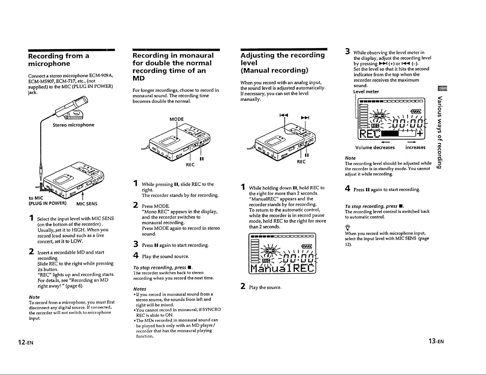
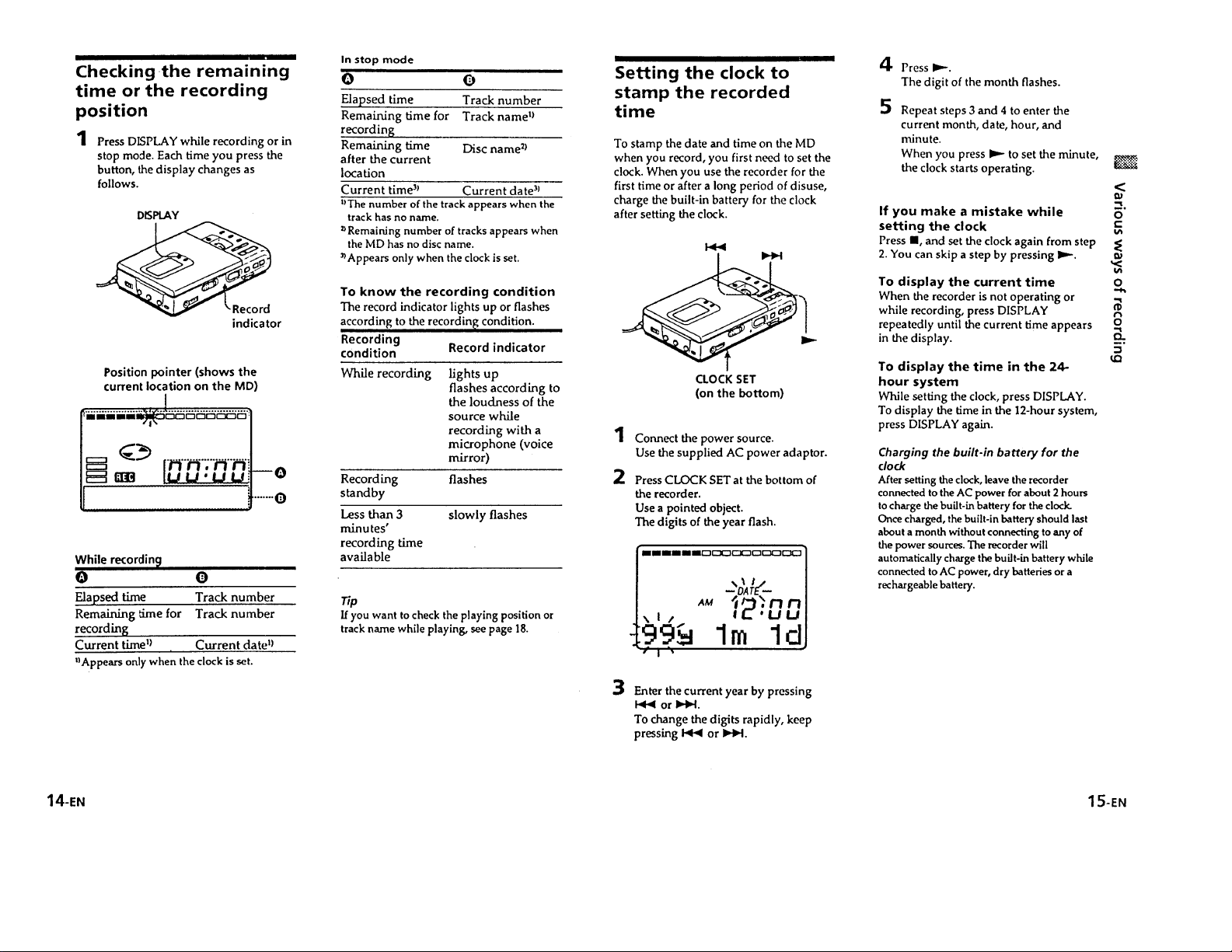
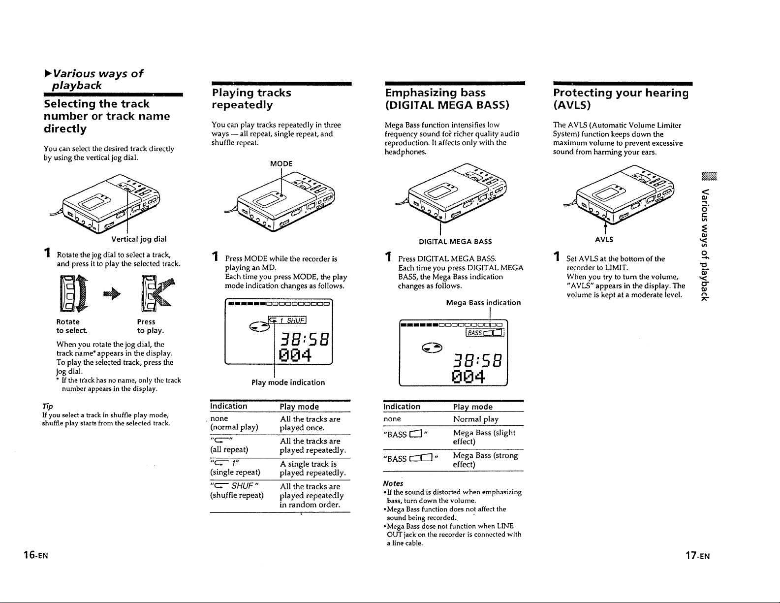
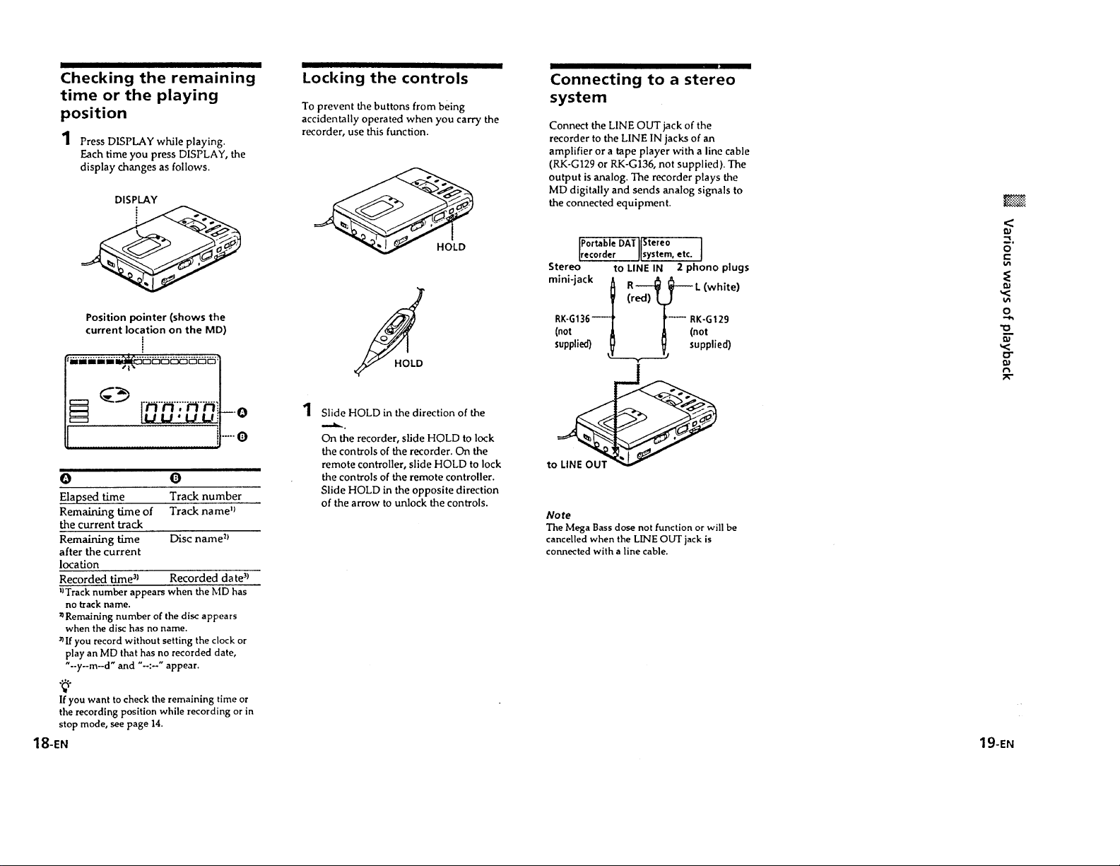
Page 1
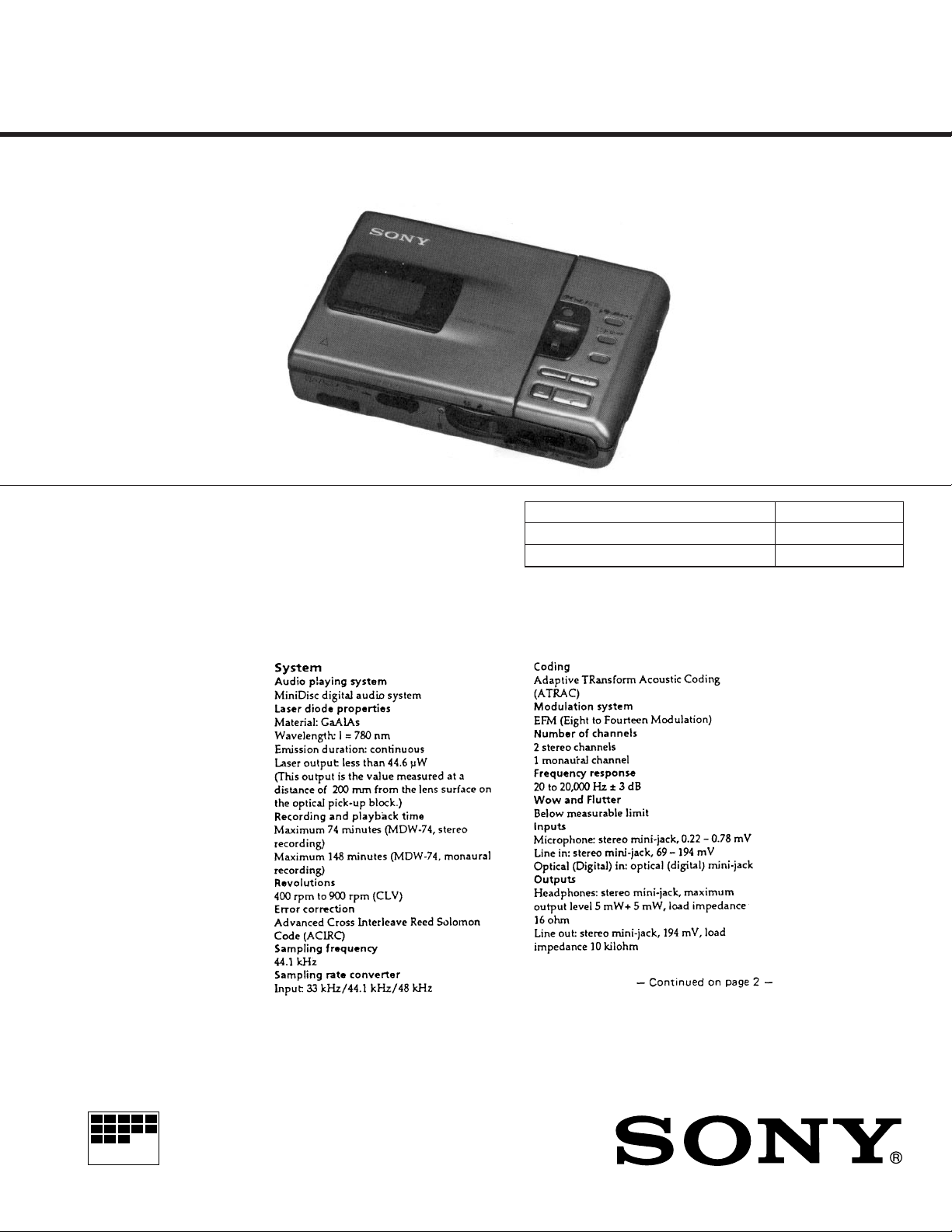
MZ-R30
SERVICE MANUAL
US and foreign patents licensed from Dolby
Laboratories Licensing Corporation.
SPECIFICATIONS
US Model
Canadian Model
AEP Model
UK Model
E Model
Austr alian Model
Tourist Model
Model Name Using Similar Mechanism NEW
MD Mechanism Type MT-MZR30-124
Optical Pick-up Type KMS-250A/J2N
MICROFILM
PORTABLE MINIDISC RECORDER
Page 2
TABLE OF CONTENTS
Specifications ............................................................................... 1
1. SERVICE NOTE .................................................................. 3
2. GENERAL ............................................................................ 4
3. DISASSEMBLY
3-1. Upper Panel Assy, Bottom Panel Assy Removal.......... 20
3-2. Main Board Removal ................................................... 20
3-3. Mechanism Deck Removal........................................... 21
3-4. Optical Pick-up Assy, Control Board,
REC Board Removal .................................................... 21
3-5. Battery Case Assy Removal ......................................... 22
3-6. Switch board, Power Board Removal........................... 22
4. TEST MODE ...................................................................... 23
5. ELECTRICAL ADJUSTMENTS ..................................... 29
6. EXPLANATION OF IC TERMINALS ............................. 33
For customers in Europe
This MiniDisc Recorder is classified as a
CLASS 1 LASER product.
The CLASS 1 LASER PRODUCT label is
located on the buttom exterior.
IN NO EVENT SHALL SELLER BE
LIABLE FOR ANY DIRECT,
INCIDENTAL OR CONSEQUENTIAL
DAMAGES OF ANY NATURE, OR
LOSSES OR EXPENSES RESULTING
FROM ANY DEFECTIVE PRODUCT
OR THE USE OF ANY PRODUCT.
“MD WALKMAN” is a trademark of Sony
Corporation.
CAUTION
Use of controls or adjustments or performance of procedures other
than those specified herein may result in hazardous radiation exposure.
Flexible Circuit Board Repairing
• Keep the temperature of the soldering iron around 270°C during
repairing.
• Do not touch the soldering iron on the same conductor of the circuit board (within 3 times).
• Be careful not to apply force on the conductor when soldering or
unsoldering.
Notes on chip component replacement
• Never reuse a disconnected chip component.
• Notice that the minus side of a tantalum capacitor may be damaged by heat.
7. DIAGRAMS
7-1. Block Diagram.............................................................. 37
7-2. Cricuit Boards Location ............................................... 41
7-3. Printed Wiring Boards – Main Section –...................... 42
7-4. Schematic Diagram – Main (1/3) Section – ................. 47
7-5. Schematic Diagram – Main (2/3) Section – ................. 51
7-6. Schematic Diagram – Main (3/3) Section – ................. 55
7-7. Schematic Diagram – Power Section – ....................... 57
7-8. Printed Wiring Boards – Control Section –.................. 60
7-9. Schematic Diagram – Control Section – ..................... 63
8. EXPLODED VIEWS
8-1. Upper Panel, Bottom Panel Section ............................. 69
8-2. Chassis Section ............................................................. 70
8-3. Mechanism Deck Section-1.......................................... 71
8-4. Mechanism Deck Section-2.......................................... 72
9. ELECTRICAL PARTS LIST ............................................ 73
SAFETY-RELATED COMPONENT WARNING!!
COMPONENTS IDENTIFIED BY MARK ! OR DOTTED LINE WITH
MARK ! ON THE SCHEMATIC DIAGRAMS AND IN THE PARTS
LIST ARE CRITICAL TO SAFE OPERATION.
REPLACE THESE COMPONENTS WITH SONY PARTS WHOSE
PART NUMBERS APPEAR AS SHOWN IN THIS MANUAL OR IN
SUPPLEMENTS PUBLISHED BY SONY.
ATTENTION AU COMPOSANT AYANT RAPPORT
À LA SÉCURITÉ!
LES COMPOSANTS IDENTIFIÉS P AR UNE MARQUE ! SUR LES
DIAGRAMMES SCHÉMA TIQUES ET LA LISTE DES PIÈCES SONT
CRITIQUES POUR LA SÉCURITÉ DE FONCTIONNEMENT. NE
REMPLACER CES COMPOSANTS QUE PAR DES PIÈCES SONY
DONT LES NUMÉROS SONT DONNÉS DANS CE MANUEL OU
DANS LES SUPPLÉMENTS PUBLIÉS PAR SONY
– 2 –
Page 3
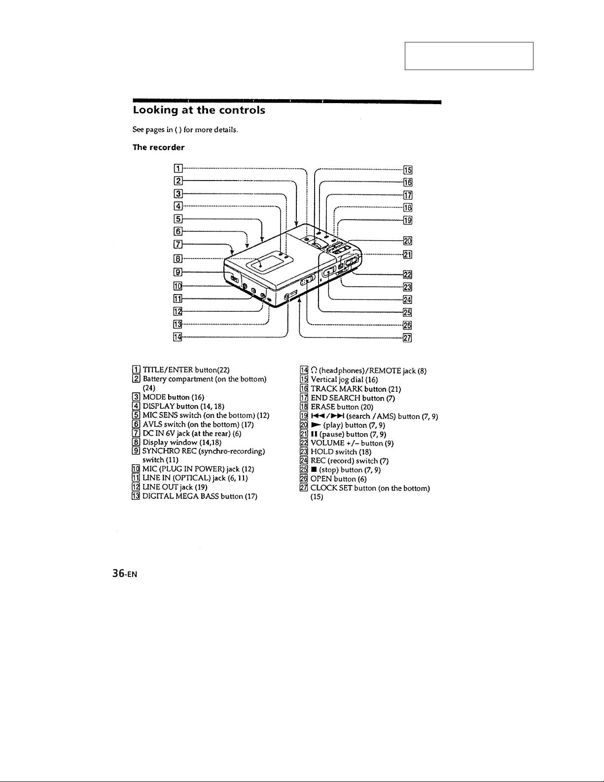
SECTION 1
SERVICING NOTE
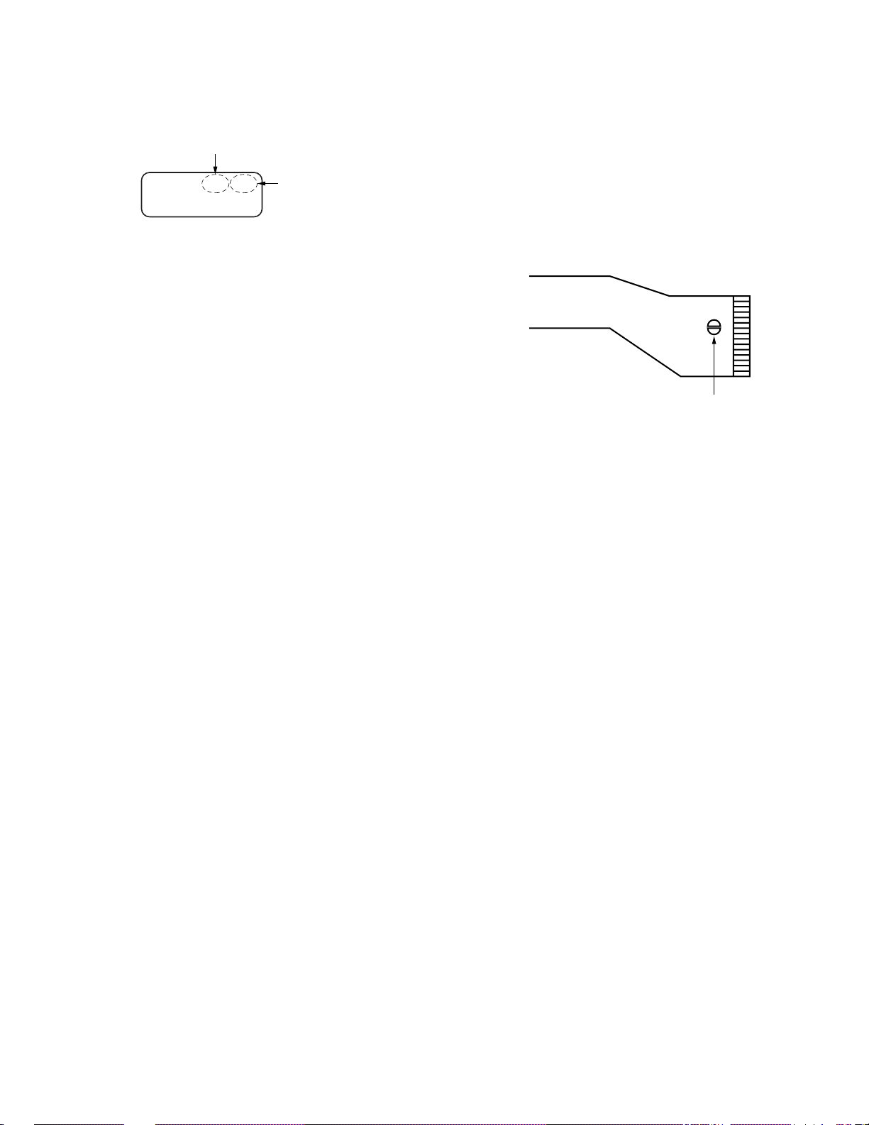
When repairing this device with the power on, if you remove the main board or open the upper panel assembly, this device stops working.
In this case, you can work without the device stopping by fastening the hook of the Open/Close detection switch (S817) with tape.
Tape
Door open/close
switch (S817)
Main board
– 3 –
Page 4
SECTION 2
GENERAL
This section is extracted from
instruction manual.
– 4 –
Page 5
– 5 –
Page 6
– 6 –
Page 7
– 7 –
Page 8
– 8 –
Page 9
– 9 –
Page 10
– 10 –
Page 11
– 11 –
Page 12
– 12 –
Page 13
– 13 –
Page 14
– 14 –
Page 15
– 15 –
Page 16
– 16 –
Page 17
– 17 –
Page 18
– 18 –
Page 19
– 19 –
Page 20
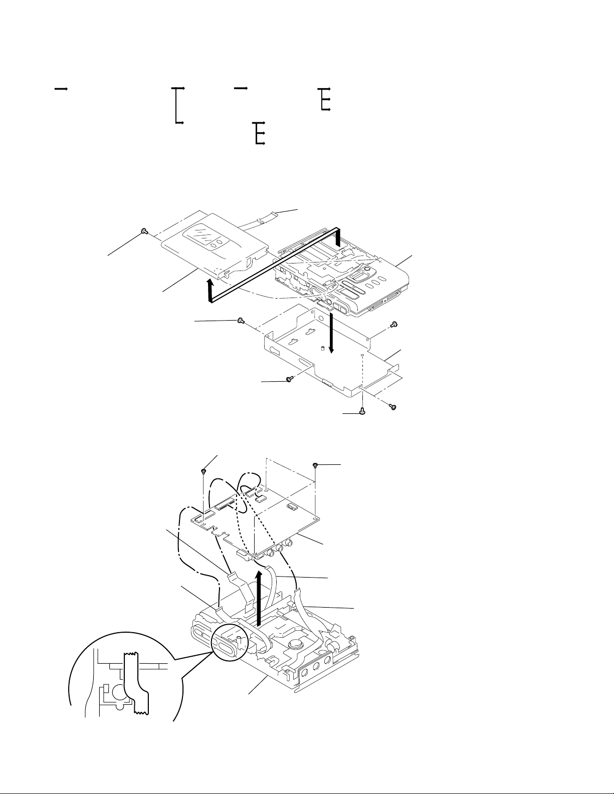
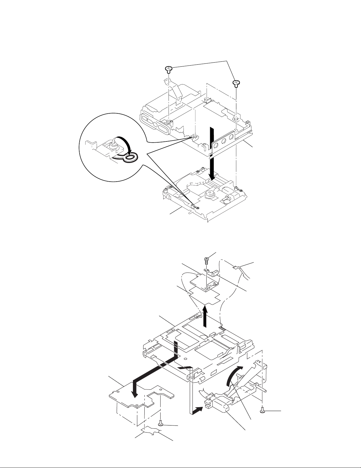
SECTION 3
DISASSENBLY
r
The equipment can be removed using the following procedure.
Set
Panel (upper, bottom) assy
Note : Follow the disassembly procedure in the numerical order given.
3-1. UPPER PANEL ASSY, BOTTOM PANEL ASSY REMOVAL
Main board Mechanism deck
Battery case assy
Switch board
Power board
Battery case
2
Optical pick-up assy
Control board
Rec board
LCD flexible board (Main board, CN905)
1
Screws
(M1.4 precision pan)
Upper panel assy
4
(M1.4 precision pan)
3-2. MAIN BOARD REMOVAL
* Note for installation
Install the main board pressing the OPEN
button on door open side.
Sometime the open/close detection switch
(S817) will be broken.
5
Flat cable
(24 core)
Screws
5
(1.7x2.5 tapping)
3
Screw
2
6
Screw
(M1.4 precision pan)
Screw (M1.7x2.5)
7
1
Screws
(M1.4 toothed lock)
Main board
Main assy
6
Screws
(M1.4 precision pan)
Bottom panel assy
6
Screws
(M1.4 precision pan)
6
OP flexible board
(Main board CN501)
Ornamental belt assy
Note for installation
*
After installing the main board, make the flexible board ride on the molding. If you hold
the flexible board and main board with a pair of tweezers, the board will ride correctly.
7
3
JOG unit flexible board
(Main board CN904)
– 20 –
4
MD frexible board
(Main board CN502)
* Note for installation
After installing the main
board, push the flexible
board to the outside with a
pair of tweezers. Otherwise,
it may be caught between
the optical pickup section and
the molding.
Page 21
3-3. MECHANISM DECK (MT-MZR30-124) REMOVAL
y
)
2
Remove the damper
fastening ring section.
Mechanism deck
1
Screws (Damper)
3
Ornamental belt ass
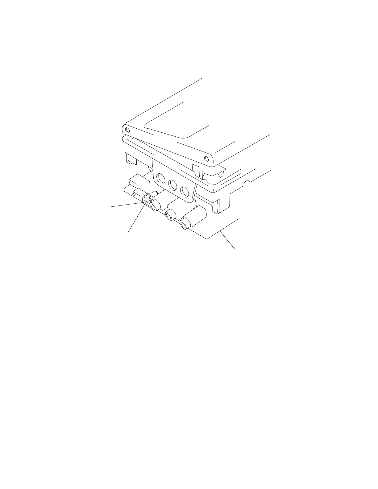
3-4. OPTICAL PICK-UP ASSY, CONTROL BOARD, REC BOARD REMOVAL
8
Screw
REC board
Insulating sheet
Control board
5
Remove solder
Mechanism deck
7
4
6
Screws (M1.4)
CLV flexible board
9
1
Head flexible board
(REC board, CN402)
Lever stopper
2
(M1.4x3, locking
3
Over wirte head
Optical pick-up assy
Screws
– 21 –
Page 22
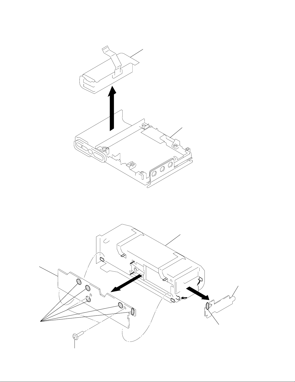
3-5. BATTERY CASE ASSY REMOVAL
t
d
Battery case assy
1
Ornamental bel
3-6. SWITCH BOARD, POWER BOARD REMOVAL
Power board
4
Remove solder
6
Battery case
2
3
2
1
Remove solder
Switch boar
5
Screws (M1.4)
– 22 –
Page 23
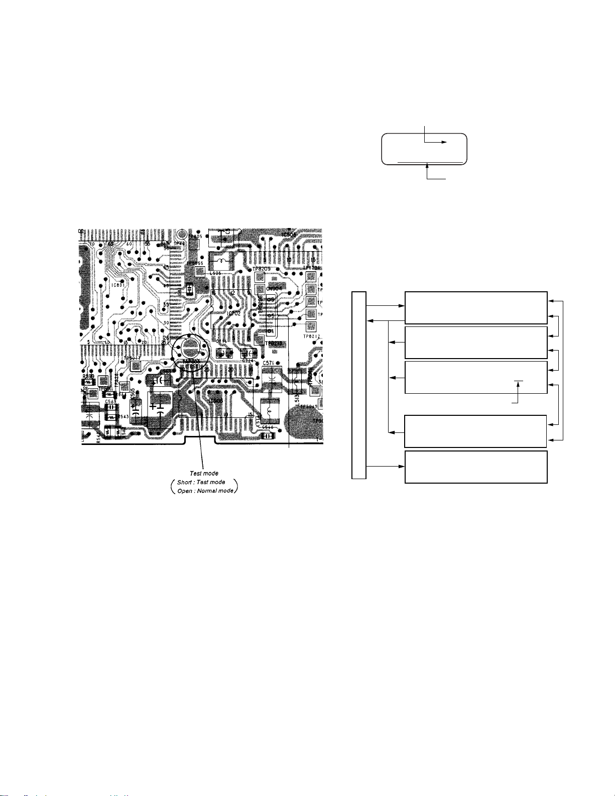
SECTION 4
p key
+ key
VOLUME +key or – key
Display when Test Mode is Set
= key
Servo Mode
Segment Section : 00
Dot Section : SERVO
Audio Mode
Segment Section : 00
Dot Section : AUDIO
Power Mode
Segment Section : 00
Dot Section : POWER
General Adjustment Mode
Segment Section : 4000
Dot Section : Assy MODE
Mecha Mode
Segment Section : 00 00
Dot Section : MECHA
Select dial number (blinks)
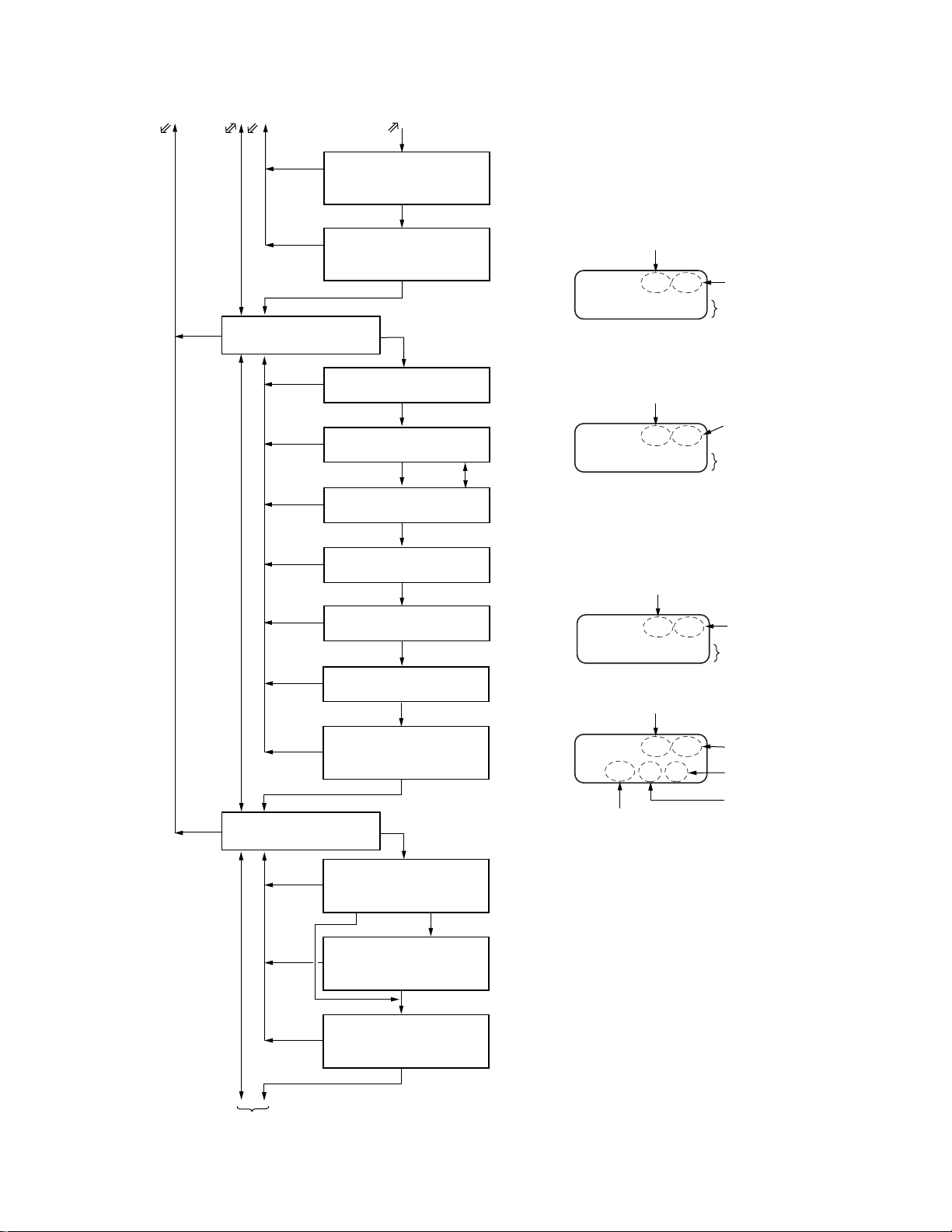
TEST MODE
[Outline]
• The general adjustment mode of this unit performs CD and MO
adjustments automatically when set. In this mode, the disc is determined if CD or MO and adjustments are automatically performed
in order. If errors are detected , the faulty locations are displayed.
The servo mode performs each adjustment automatically.
[Setting the Test Mode]
Short-circuit the soldering bridge of TAP803 (TEST) on the main
board (connect Pin @§ of IC801 to the GND) and turn on the power
supply.
[MAIN BOARD] (SIDE A)
[Operations When Test Mode is Set]
When the test mode is set, the LCD will display as follows.
Self-diagnostic display
(displayed while the DISPLAY key is pressed)
Segment section
00
Ver 00.75
Dot section
ROM version displayed
• The LCD performs the following repeatedly.
ROM version displayed / all lit / all off
• The display can be held and checked by pressing P key.
• The self-diagnostic display appears while the DISPLAY key is
pressed.
[Structure of Test Mode]
The test mode of this unit consists of the following five modes.
[Exiting the Test Mode]
Turn off the power supply and open the soldering bridge of TAP803
(TEST) on the main board.
• In modes other than the general adjustment mode, the last two digits of the mode number will be displayed at the 00 section.
– 23 –
Page 24
[Servo Mode]
• Set the test mode, press the + key, and set the servo mode using
the VOLUME + and – keys.
• When the servo mode is set, the optical pickup will move to the
outer circumference or inner circumference if the + key or =
key is pressed.
• To set other modes, refer to “ Structure of Test Mode ”.
• Structure of Servo Mode
Mode : 000
Servo mode
p key
p key
p key
VOLUME +key or –key
” key
Mode : 010
M
Offset compensation
value displyed
p key
VC offset compensation
p key
FE offset compensation
p key
APC offset compensation
p key
VOLUME +key or – key
p key
p key
Mode : 020
M
Laser power adjustment
p key
p key
VOLUME +key or – key
Mode : 030
M
MO playback recording
adjustment
ABCD offset compensation
Laser MO read adjustment
Laser MO write adjustment
1
(To page 25)
” key
Mode : 011
M
” key
Mode : 012
M
” key
Mode : 013
M
” key
Mode : 014
M
” key
Mode : 015
All servo ON
M
” key
Mode : 016
Temperature display
M
” key
” key
Mode : 021
M
” key
Mode : 022
M
” key
” key
2 3 4 5
*1:+ key
:= key
*2:REC key
VOLUME +key or – key
p key
Low reflection CD playback
VOLUME +key or – key
p key
p key
p key
p key
p key
p key
p key
p key
Mode : 040
M
adjustment
p key
p key
p key
p key
p key
MO tracking gain adjustment
Low reflection CD EF balance adjustment
Low reflection CD ABCD level adjustment
Laser Low reflection CD read adjustment
Low reflection CD focus gain adjustment
Mode : 032
MO playback EF balance adjustment
*2
Mode : 033
MO playback ABCD level adjustment
*2
Mode : 034
MO recording EF balance adjustment
*2
Mode : 035
MO recording ABCD level adjustment
*2
Mode : 036
Laser MO read adjustment
Mode : 037
MO focus gain adjustment
Mode : 038
Mode : 039
MO focus bias variable
(Cluster Display)
Mode : 041
Low reflection CD focus serch ON
Mode : 042
Mode : 043
Mode : 044
Mode : 045
M
M
M
M
M
M
M
M
” key
M
” key
” key
” key
” key
” key
” key
” key
” key
” key
” key
” key
” key
” key
*1
*1
*1
p key
or – key
VOLUME +key
2 3 4 5
Mode : 031
MO focus search ON
M
6 7 8 9
(To page 25) (To page 25) (To page 25)
” key
– 24 –
Page 25
6 7 8 9
VOLUME +key or – key
p key
CD playback adjustment
*1:+ key
:= key
VOLUME +key or – keyVOLUME +key or – key
p key
p key
p key
Mode : 050
M
p key
p key
p key
p key
p key
p key
p key
Mode : 060
Full REC
CD tracking gain adjustment
Mode : 046
Low reflection CD tracking
gain adjustment
Mode : 047
Low reflection CD focus bias variable
(Cluster Display)
Mode : 051
CD focus search ON
Mode : 052
CD EF balance adjustment
Mode : 053
CD ABC level adjustment
Mode : 054
Laser CD read adjustment
Mode : 055
CD focus gain adjustment
Mode : 056
Mode : 057
CD focus bias adjustment
(Cluster Display)
M
” key
M
” key
” key
” key
” key
” key
” key
” key
” key
” key
” key
• Adjusting Method
Note : There is basically no display for individual adjustment items.
1. When the adjustment modes are set according to “Structure of
Servo Mode”, the last two digits of the mode number and the adjustment value written in the EEPROM will be displayed blinking.
2. When the P key is pressed, the following will be displayed and
adjustments will be performed automatically.
*1
Note : The adjustment value can be changed as desired using the
3. After the adjustments are completed, the item is displayed again
and the adjustment value that was blinking lights up.
• Cluster Display
• Nothing is performed at mode numbers 070 to 073.
Only such upper position titles as SER VO, AUDIO, etc.
(100s position) are displayed.
Mode No. (Last 2 digits)
52 09
Mode No. (Last 2 digits)
52 09
AUTO_ADJ
Adjustment value
(Blinks)
Display of item
Adjustment value
(Blinks)
Automatic adjustment
being performed
VOLUME + and – keys, but try to avoid this as much as
possible.
Mode No. (Last 2 digits)
52 08
Mode No. (Last 2 digits)
52 09
026 4B 01
Cluster value
Adjustment value
(Lights)
Display of item
Adjustment value
(Blinks)
BLOCK error rate
AT error rate
*2:REC key
1
(To page 24)
p key
p key
p key
Mode : 061
32 cluster full REC
(Cluster Display)
” key
Mode : 062
REC shock
(Cluster Display)
” key
Mode : 063
32 cluster PLAY
(Cluster Display)
” key
*2
– 25 –
Page 26
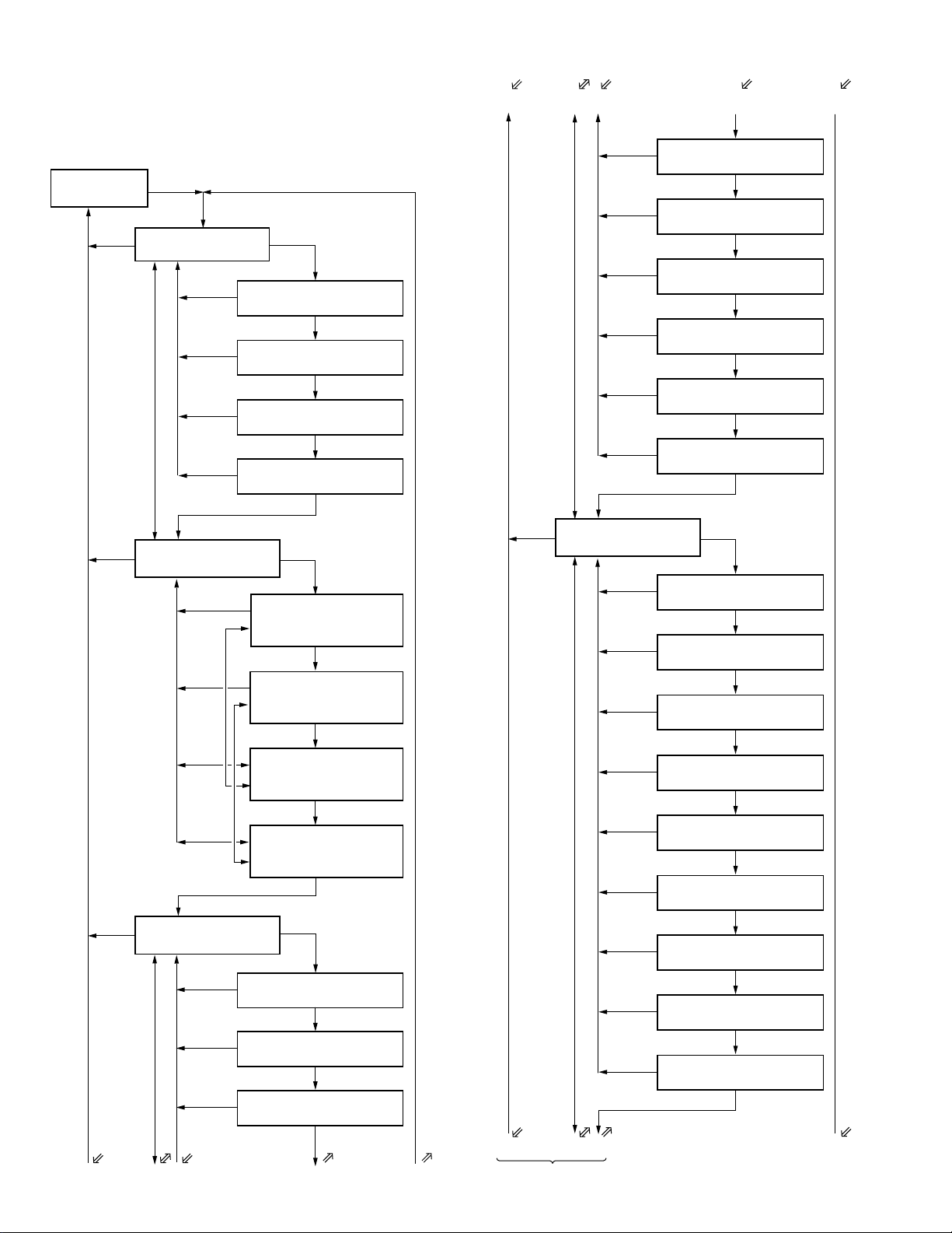
[Audio Mode]
1
23
4
5
VOLUME +key or – keyVOLUME +key or – key
p key
” key
M
Mode : 140
Digital AGC Adjustment 2
p key
M
Mode : 134
MIC GAIN
” key
p key
M
Mode : 135
MIC ATTACK
” key
p key
M
Mode : 136
MIC RECOVER
” key
p key
M
Mode : 137
MIC THD2
” key
p key
M
Mode : 138
MIC GAIN 2
” key
p key
Mode : 141
LINE UP SR
” key
p key
Mode : 142
LINE DOWN SR
” key
p key
Mode : 143
LINE THD0
” key
p key
Mode : 144
LINE GAIN
” key
p key
Mode : 145
LINE ATTACK
” key
p key
Mode : 146
LINE RECOVER
” key
p key
Mode : 147
LINE THD2
” key
p key
Mode : 148
LINE GAIN2
” key
p key
Mode : 149
LINE RTIME
” key
p key
M
Mode : 139
MIC RTIME
” key
1 2 3 4 5
6 7 8 9
(To page 27) (To page 27)
• Set the test mode, press the + key, and set the audio mode using
the VOLUME + and – keys.
• To set other modes, refer to “Structure of Test Mode”.
• Structuer of Audio Mode
Mode : 100
Audio mode
p key
VOLUME +key or – key
p key
p key
VOLUME +key or – key
” key
Mode : 110
M
Audio playback test
p key
p key
p key
p key
Mode : 120
M
Audio recording test
p key
p key
p key
VOLUME +key or – key
p key
Mode : 130
M
Digital AGC adjustment 1
p key
p key
p key
DEMP Manual recording
REC key REC key
DEMP AGC recording
” key
Mode : 111
L&R 1kHz 0dB
M
” key
Mode : 112
L 1kHz 0dB R-
M
” key
Mode : 113
L-
∞
R 1kHz 0dB
M
” key
Mode : 114
L&R-
∞
M
” key
” key
Mode : 121
Manual recording
(LINE, MIC)
” key
Mode : 122
(LINE, MIC)
” key
Mode : 123
AGC recording
(LINE, OPT, MIC)
” key
Mode : 124
(LINE, OPT, MIC)
” key
” key
Mode : 131
MIC UP SR
M
” key
Mode : 132
MIC DOWN SR
M
” key
Mode : 133
MIC THDO
M
” key
∞
– 26 –
Page 27
6 7 8 9
” key
p key
p key
” key
Mode : 200
Mecha Mode
M
Mode : 210
Mechanism check
M
Mode : 211
EJECT prohibited
p key
” key
M
Mode : 212
Magnetic head ON
” key
[Mecha Mode]
• Set the test mode, press the + key, and set the mecha mode
using the VOLUME + and – keys.
• To set other modes, refer to “Structure of Test Mode”.
p key
Mode : 150
M
Digital AGC Adjustment 3
p key
p key
p key
p key
AUTO LMT UP SR
p key
AUTO LMT DOWN SR
p key
p key
MANU LMT UP SR
p key
MANU LMT DOWN SR
p key
” key
Mode : 151
MAN UP SR
” key
Mode : 152
MAN DOWN SR
” key
Mode : 153
AUT O THD3
” key
Mode : 154
” key
Mode : 155
” key
Mode : 156
MAN THD3
” key
Mode : 157
” key
Mode : 158
” key
Mode : 159
THD1
” key
• When the P key is pressed at mode numbers 100, 110 to 114, the
buzzer will sound.
• When the VOLUME keys + and – are pressed at mode numbers
111 to 113, 123, 124, the volume of the headphone output will
increase/decrease.
When the = key or + key is pressed, the volume of the head-
phone output will become maximum/minimum.
• When the VOLUME keys + and – are pressed at mode numbers
121 or 122, the recording level will increase/decrease.
When the = key or + key is pressed, the recording level will
become maximum/minimum.
• At mode numbers 121 to 124, the recording LED will light up.
• At mode numbers 121 to 124, the microprocessor will detect the
port and automatically determine the input.
• Structure of Mecha Mode
• At mode numbers 200, 210 to 212, the optical pick up can be moved
to the outer circumference or inner circumference using the =
or + key.
[Power supply Mode]
• Set the test mode, press the + key, and set the power supply
mode using the VOLUME + and – keys.
• To set other modes, refer to “Structure of Test Mode”.
• Structure of Power Supply Mode
Mode : 300
Power supply mode
p key
” key
Mode : 310
M
Power supply
discrimination test
” key
(Automatic discrimination)
p key
p key
VOLUME +key or – key
p key
p key
Mode : 311
Ni MH
Mode : 312
AM3 ✕ 2
Mode : 313
DC IN
Mode : 314
EXT BATT
” key
” key
” key
” key
– 27 –
p key
Mode : 320
Charge test
” key
Mode : 321
Main Charge
p key
Page 28
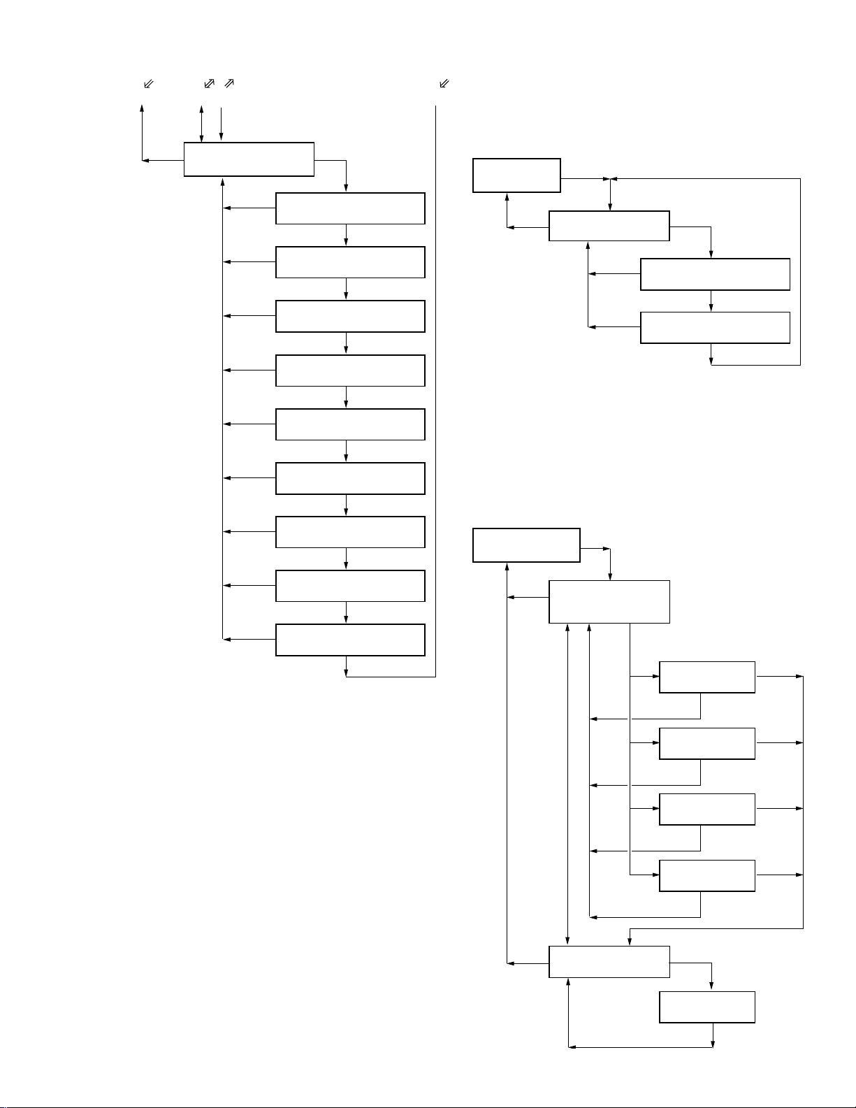
[General Adjustment Mode]
• Set the test mode, press the = key, and set the general adjust-
ment mode.
• To set other modes, cut of f the power once and power on again.
• When the general adjustment mode is set, the LCD display will be
as follows.
4000
Assy MODE
• Structure of General Adjustment Mode
General
adjustment mode
” key (CD, MO discrimination)
CD automatic
adjustment
p key
OK
NG
” key
p key
• MO Automatic Adjustment
No. Mode No. Adjustment
1 032 MO playback EF balance adjustment
2 033 MO playback ABCD level adjustment
3 034 MO recording EF balance adjustment
4 035 MO recording ABCD level adjustment
5 037 MO focus gain adjustment
6 038 MO tracking gain adjustment
7 061 32 cluster full REC
8 062 REC shock
9 063 32 cluster PLAY
10 039 MO focus bias adjustment
11 042 Low reflection CD EF balance adjustment
12 043 Low reflection CD ABCD level adjustment
13 045 Laser low reflection CD read adjustment
14 046 Low reflection CD tracking gain adjustment
MO automatic
adjustment
p key
Reset
OK
NG
” key
p key
Adjusting Method :
1. Set the test mode, press the = key to set the general adjustment
mode.
2. Load the CD test disc (TDYS-1) or SONY MO disc available on
the market.
3. When the ” key is pressed, the disc is determined if CD or MO,
the automatic adjustment modes are set, and adjustments are performed automatically in the following order.
• CD Automatic Adjustment
No. Mode No. Adjustment
1 052 CD EF balance adjustment
2 053 CD ABCD level adjustment
3 055 CD focus gain adjustment
4 056 CD tracking gain adjustment
5 057 CD focus bias adjustment
* Display during MO automatic adjustment
37
Mode No.
during adjustment
MO RUN
4. If the automatic adjustment results are OK, the following will be
displayed.
00
CD mode OK
5. If the automatic adjustment results are NG, the following will be
displayed.
NG mode No. (Last 2 digits)
55 7F
Adjustment results
CD mode NG
* When the mode number is 039, 057 and the focus bias value is
NG, the following will be displayed.
Mode No. (Last 2 digits)
57 30
Focus bias value
CD mode NG
77 : focus bias
Displayed while the P key is
pressed
* Display during CD automatic adjustment
51
Mode No.
during adjustment
CD RUN
– 28 –
77 01
CD mode NG
Error code
(01 to 04)
Page 29
SECTION 5
ELECTRICAL ADJUSTMENTS
* When the mode number is 039, 061 and the AT error rate is NG,
the following will be displayed.
Mode No. (Last 2 digits)
39 03
AT error value
CD mode NG
* When NG, set the servo mode and perform the automatic adjust-
ment of the NG item. (Refer to “Servo Mode”)
5-1. Precautions for Laser Diode Emission Check
When checking the emission of the laser diode during adjustments,
never view directly downwards as this may lead to blindness.
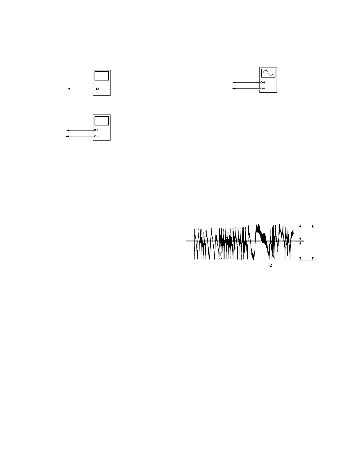
5-2. Precautions for Using Optical Pickup
(KMS–250A/J2N)
As the laser diode inside the optical pickup damages by static electricity easily, solder the laser tap of the flexible board when handling.
Also take the necessary measures to prevent damages by static electricity. Handle the flexible board with care as it breaks easily
Laser tap
Optical Pickup flexible board
5-3. Precautions for Adjustment
1) Perform all adjustments in the order given in the test mode.
After adjusting, exit the test mode.
2) Use the following tools and measuring instruments.
• CD test disc TDYS-1
(Parts Code : 4-963-646-01)
• Recorded MO disc PTDM-1
(Parts Code : J-2501-054-A)
• Laser power meter LPM-1
(Parts Code : J-2501-046-A)
• Oscilloscope (Frequency band above 40MHz. Perform the cali-
bration of probe first before measuring.)
• Digital voltmeter
3) Unless specified othewise, supply DC 6V from the DC IN 6V
jack.
4) Swtich, knob positions
Hold switch...................... OFF
AVLS switch.................... OFF
– 29 –
Page 30
5-4. Laser Power Check
r
e
Connection :
Optical pickup
objective lens
Laser
power meter
5-5. MO Traverse Adjustment
Connection :
Oscilloscop
MAIN board
TP5980 (TE)
AP5430 (VC)
Digital voltmete
MAIN board
AP5022 (VCC)
AP574 (LDIO)
Adjusting Method :
1. Set the servo mode of the test mode (Mode : 000).
2. Press the ” key, and set the laser power adjustment mode (Mode
: 020) using the volume + and – keys.
3. Press the = key and move the optical pickup to the inner most
circumference.
4. Open the cover and set the laser power meter on the objective lens
of the optical pickup.
5. Press the ” key, and set the laser MO read adjustment mode (Mode
: 021).
6. Check that the laser power meter reading is 0.85 ±0.085mW.
7. Check that the voltage between AP5022 (VCC) and AP574
(LDIO) at this time is below 44mV.
8. Press the ”key, and set the laser MO write adjustment mode (Mode
: 022).
9. Check that the laser power meter reading is 6.8 ±0.68mW.
10.Press the P key to finalize the adjustment data.
11.Check that the voltage between AP5022 (VCC) and AP574
(LDIO) at this time is below 88mV.
12.Press the p key.
13.Exit the test mode.
Adjusting Method :
1. Set the servo mode of the test mode (Mode : 000).
2. Press the ” key, and set the MO playback adjustment mode (Mode
: 030) using the volume + and – keys.
3. Press the = and + keys and move the optical pickup to the
center circumference.
4. Load any MO disc available on the market.
5. When the ” key is pressed, the MO playback EF balance adjust-
ment mode (Mode : 032) will be set after focus search ON (Mode
: 031).
6. Press the P key to perform automatic adjustment, and check that
the traverse waveform is symmetrical at the top and bottom.
7. Slide the recording key and set the MO recording EF balance adjustment mode (Mode : 034).
8. Press the P key to perform automatic adjustment, and check that
the traverse waveform is symmetrical at the top and bottom.
(Traverse Waveform)
A
0V
Specification : A = B, C 1.0 Vp-p
C
B
9. Check that the traverse level at this time is above 1.0Vp-p.
10.Press the p key.
11.Exit the test mode.
Note : Using a recorded disc in this adjustment will erase the data.
– 30 –
Page 31

5-6. Low Reflection CD Traverse Adjustment
e
e
Connection :
Oscilloscop
MAIN board
TP5980 (TE)
AP5430 (VC)
5-7. CD Traverse Adjustment
Connection :
Oscilloscop
MAIN board
TP5980 (TE)
AP5430 (VC)
Adjusting Method :
1. Set the servo mode of the test mode (Mode : 000).
2. Press the ” key, and set the low reflection CD playback adjust-
ment mode (Mode : 040) using the volume + and – keys.
3. Load any MO disc available on the market.
4. When the ” key is pressed, the low reflection CD playback EF
balance adjustment mode (Mode : 042) will be set after low reflection CD focus search ON (Mode : 041).
5. Press the P key to perform automatic adjustment, and check that
the traverse waveform is symmetrical at the top and bottom.
(Traverse Waveform)
A
0V
Specification : A = B, C 0.9 Vp-p
C
B
6. Check that the traverse level at this time is above 0.9Vp-p.
7. Press the p key.
8. Exit the test mode.
Adjusting Method :
1. Set the servo mode of the test mode (Mode : 000).
2. Press the ” key, and set the CD playback adjustment mode (Mode
: 050) using the volume + and – keys.
3. Press the = and + keys and move the optical pickup to the
center circumference.
4. Load a CD test disc (TDYS-1).
5. When the ” key is pressed, the CD playback EF balance adjust-
ment mode (Mode : 052) will be set after CD focus search ON
(Mode : 051).
6. Press the P key to perform automatic adjustment, and check that
the traverse waveform is symmetrical at the top and bottom.
(Traverse Waveform)
A
0V
B
Specification : A = B, C 1.0 Vp-p
7. Check that the traverse level at this time is above 1.0Vp-p.
8. Press the p key.
9. Exit the test mode.
C
– 31 –
Page 32

5-8. CD RF Level Check
r
Connection :
Oscilloscope
MAIN board
AP5500 (RF)
AP5430 (VC)
Digital voltmete
MAIN board
AP5022 (VCC)
AP574 (LDIO)
Adjusting Method :
1. Set the servo mode of the test mode (Mode : 000).
2. Press the ” key, and set the CD playback adjustment mode (Mode
: 050) using the volume + and -keys.
3. Press the = and + keys and move the optical pickup to the
center circumference.
4. Load a CD test disc (TDYS-1).
5. When the ” key is pressed, the CD EF balance adjustment mode
(Mode : 052) will be set after CD focus search ON (Mode : 051).
6. When the ” key is pressed, the ABCD level adjustment mode
(Mode : 053) is set.
7. Press the P key to perform automatic adjustment, and check that
the RF level is 1.0 ±0.3Vp-p.
Adjustment Location :
(RF waveform)
1.0 ± 0.3 Vp-p
8. Check that the voltage between AP5022 (VCC) and AP574
(LDIO) at this time is below 44mV.
9. Press the p key.
10.Exit the test mode.
– 32 –
Page 33

SECTION 6
EXPLANATION OF IC TERMINALS
IC503 DIGITAL SERVO, ATRAC (CXD2652R)
Pin No. Pin name I/O Description
1 MNT 0 O Traverse count signal output.
2 MNT 1 O Track jump detect output.
3 MNT 2 – Not used (Open).
4 MNT 3 – Not used (Open).
5 SWDT I Inputs write data signal from system controller (IC801).
6 SCLK I Inputs serial clock signal from system controller (IC801).
7 XLAT I Inputs serial latch signal from system controller (IC801).
8 SRDT O Outputs write data signal to system controller (IC801).
9 SENS O Outputs internal status (SENSE) to system controller (IC801).
10 XRST I Inputs reset signal from system controller (IC801). Reset : L
11 SQSY O
12 DQSY O
13 WRPWR I Inputs laser power switching signal from system controller (IC801).
14 NC – Not used (Open).
15 TX I
16 OSC1 O Clock output (45MHz).
17 OSC0 I Clock input (45MHz).
18 XTSL – Not used (Fixed at “L”)
19 RVDD – Not used (Open).
20 RVSS – Connect to ground.
21 DIN I Digital audio signal input pin (For optical input).
22 NC – Not used (Open).
23 ADDT I Audio data input from A/D converter (IC303).
24 DATA O Monitor/decode audio data output to A/D converter (IC303).
25 ALRCK O L/R clock output to D/A converter (IC303).
26 ABCK O Bit clock signal output to A/D, D/A converter (IC303).
27 FS256 O 11.2896MHz clock output (MCLK).
28 DVDD – Power supply (+2.8V) for digital.
29 – 32 A03 – A00 O Address signal output to RAM (IC509).
33 NC – Not used (Open).
34 – 38 A04 – A08 O Address signal output to RAM (IC509).
39 NC – Not used (Open).
40 DVSS – Ground terminal.
41 XOE O Output enable contol signal output to RAM (IC509).
42 XCAS O Column address strobe singal output to RAM (IC509).
43 A09 O Address signal output to RAM (IC509).
44 XRAS O Row address strobe signal output to RAM (IC509).
45 XWE O Read/write control signal output to RAM (IC509).
46 – 49 D1 – D3 I Data signal input from RAM (IC509).
50 MVCI – Not used (Connect to ground).
51 ASYO O Playback EFM full-swing output (L : VSS, H : VDD).
52 ASYI I Playback EFM asymmetry comparate voltage input.
Output subcode Q sync (SCOR) to system controller (IC801).
Outputs “L” every 13.3msec. Outputs “H” at all most mostly.
Outputs digital-in U-bit CD format subcode Q sync (SCOR) to system controller (IC801).
Outputs “L” every 13.3msec. Outputs “H” at all most mostly.
Input of write data taransmission timing from system controller (IC801).
Also used as magnetic field head ON/OFF output.
– 33 –
Page 34

Pin No. Pin name I/O Description
53 AVDD – Power supply (+2.8V) for analog.
54 BIAS I Playback EFM asymmetry circuit constant current input.
55 RFI I Inputs playback EFM RF signal from RF amplifier (IC501).
56 AVSS – Ground terminal.
57 PDO – Not used (Open).
58 PCO O Decoder PLL master clock PLL phase comparison output.
59 FILI I Decoder PLL master clock PLL filter input.
60 FILO O Decoder PLL master clock PLL filter output.
61 CLTV I Decoder PLL master clock PLL VCO control voltage input.
62 PEAK I Inputs peak hold signal for light amount signal from RF amplifier (IC501).
63 BOTM I Inputs bottom hold signal for light amount signal from RF amplifier (IC501).
64 ABCD I Light amount signal from RF amplifier (IC501).
65 FE I Input focus error signal from RF amplifier (IC501).
66 AUX1 I Input of auxiliary signal from RF amplifier (IC501).
67 VC I Input of middle point voltage (+1.4V) from RF amplifier (IC501).
68 ADIO – Not used (Open).
69 AVDD – Power supply (+2.8V) for analog.
70 ADRT – Not used (Connect to +2.8V).
71 ADRB – Not used (Open).
72 AVSS – Ground terminal.
73 SE I Input of sled error signal from RF amplifier (IC501).
74 TE I Input of tracking error signal from RF amplifier (IC501).
75 AUX2 – Not used (Open).
76 DCHG – Not used (Connect to +2.8V).
77 APC – Not used (Connect to +2.8V).
78 ADFG I
79 FO CONT O Focus control output to RF amplifier (IC501).
80 XLRF I Latch signal input from RF amplifier (IC501).
81 CKRF O RFCK clock (7.35kHz) signal output.
82 DTRF I Serial data input from system controller (IC801).
83 APCREF I Laser power setting signal input.
84 LDDR – Not used (Open).
85 TRDR O Tracking servo drive signal output (–).
86 TFDR O Tracking servo drive signal output (+).
87 DVDD – Power supply (+2.8V) for digital.
88 FFDR O Focus servo drive signal output (+).
89 FRDR O Focus servo drive signal output (–).
90 FS4 O 176.4kHz clock signal output (MCLK).
91 SRDR O Sled servo drive signal output (–).
92 SFDR O Sled servo drive signal output (+).
93 SPRD O Spindle servo drive signal output (–).
94 SPFD O Spindle servo drive signal output (+).
95 FGIN I FG signal input from spindle motor driver (IC701).
96 TEST1 – Not used (Connect to +2.8V).
97 TEST2 – Not used (Connect to +2.8V).
98 TEST3 – Not used (Connect to +2.8V).
99 DVSS – Ground terminal.
100 EFMO O EFM recording signal ouput.
Input of ADIP dual FM signal from RF amplifier (IC501) (22.05kHz±1kHz).
(TTL Schmidt input)
– 34 –
Page 35

IC801 SYSTEM CONTROL (CXP81960M-632R)
Pin No. Pin name I/O Description
1 CLCS O Chip select output to real time clock (IC804).
2 XRST O Reset output. L : Reset
3 WRPWR – Laser power switching signal output.
4 TX O Write data transfer timing output.
5 SENSE I Internal status (SENSE) input.
6 LDON O Laser ON signal. H : ON
7 XSHOCK I Track jump detection input.
8 PIT/GRV I COMP signal input from RF amplifier (IC501).
9 INLS I Detecting switch for internal circuit of sleding. Internal circuit : L
10 PROTECT I Disc write protect switch. H : Protect
11 DATA O Data output to remote control.
12 HOLD I Hold switch input (This unit). L : Hold
13 WP I Wake-up signal input from remote control key and this unit key.
14 OPEN I Detecting switch for opening and closing of the upper cover. Close : L
15 CLOCK I CLOCK SET switch input.
16 CLSDIO I Serial clock input.
17 SDIO2 I/O Serial data input/output.
18 PUSH JOG I Push JOG switch input.
19 LCD STB O LCD standby ouput.
20 CLSCK O Serial clock output for real time clock (IC804).
21 SDI2 I Serial data input.
22 SYNC. REC I SYNCHRO REC switch input.
23 D. B. B I DIGITAL MEGA BASS switch input.
24 LINEDET I Line input detect. L : Line
––––––––––––––––––––
25 AVLS I AVLS switch input. L : ON
26 TEST I Test mode terminal. L : Test mode
27 DCIN I DC input detect. L : DC IN
––––––––––––
28 KANASE L – Not used (Connect toground).
29 –––– – Not used (Open).
30 PCONT O Power control output. L : ON
31 BATTON O Outputs L while operating with a battery.
–––––––––––––––
––––––––––––––––––
32 RECLED O REC LED control. L : ON
33 MODE2 O
34 MODE1 O
Head drive (IC506) control signal output.
35 RFSW O Power control output to RF amplifier (IC501).
36 LCD ON O LCD ON/OFF control. L : ON
–––––––––––––––––
37 MP – Microprocessor mode input (Fixed at “L”).
38 MRST I Microprocessor reset input.
–––––––––––––
39 VSS – Ground.
40 XTAL – System clock (12MHz).
41 EXTAL – System clock (12MHz).
42 CS – Chip Select input (Connected to +2.8V).
43 –––– – Not used (Fixed at “L”).
44 LCDDATA O LCD data output.
45 LCDSCK O Serial clock output.
46 LI-MNT I Voltage monitor for lithium battery.
47 FDMON I Focus coil position monitor input.
48 HIDCMNT I Voltage monitor DC input.
49 KEY2 I Remote control key input.
50 AVSS – A/D converter ground terminal.
– 35 –
Page 36

Pin No. Pin name I/O Description
51 AVREF I A/D converter reference voltage input.
52 AVDD – A/D converter power supply terminal.
53 AM3 I AC adaptor or EXT battery detection input. L : EXT battery
54 TEMP I Temp meter (IC803) input.
55 KEY3 I PLAY Key input.
56 KEY4 I Key input.
57 KEY0 I Key input.
58 KEY1 I Key input.
59 UNMNT (LI+MNT) I UNREG voltage monitor.
60 LIMIT (LI+MNT) I Voltage monitor for lithium battery.
61 FGIN I FG input from motor driver (IC701).
62 SLA I
63 SLB I
JOG dial signal input.
64 INTSW I INITIAL switch input.
65 P ACK IN I MEDIA switch input.
66 JACKDET I Input jack detection input.
––––––––––––––––––––
67 OPT DET I Detecting input an optical input.
68 MICDET I MIC jack detection.
69 XLAT O Latch output.
70 KEYON O TRACK MARK jack input.
71 ST1SOU O
72 ST2SOU O
Stepping motor signal output.
73 XAMON O Charge current control.
74 –––– – Not used (Open).
75 DQSY I Subcode Q sync (SCOR) of digital in U-bit CD format from IC503.
76 TCOUNT I Traverse count signal input.
77 SDI1 I Serial data input.
78 SDO1 O Serial data output.
79 SCK1 O Serial clock output.
80 SQSY I SUB-Q/ADIP SYNC input.
81 BEEP O BEEP sound output control. H : BEEP sound output
82 –––– – Not used (Open).
83 REFLCT I CD/MO discrimination switch.
84 TEX – Not used (Fixed at “L”)
85 XT – Not used (Open).
86 VSS – Ground.
87 VDD – Power supply pin (+2.8V).
88 NC – Not used (Fixed at “H”)
89 CS I Chip select input.
90 PD O D/A converter power down detect during recording. H : Power down
––––––––
––––––––
91 –––– – Not used (Open).
92 –––– – Not used (Open).
93 AMUTE O Analog mute control. L : Mute
94 OPTCONT O Power supply control output for an optical input.
95 CSHP O
96 CSNV O
Chip select output.
97 SCK2 O Serial clock output.
98 XMODON O HF module control output.
99 SDO2 O Serial data output.
100 LI–CHG O Charge control. H : Charge
– 36 –
Page 37

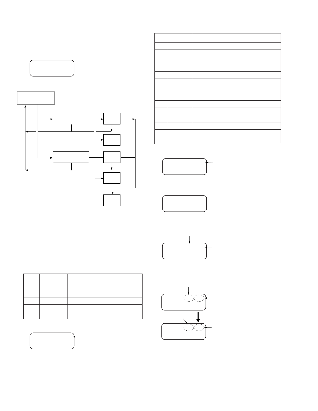
7-1. BLOCK DIAGRAM
d
SECTION 7
MZ-R30
DIAGRAMS
7-2. CIRCUIT BOARDS LOCATION
REC board
CONTROL board
MAIN board
SWITCH board
POWER boar
• Signal path.
: PB
: REC
: MIC
– 37 – – 38 – – 39 – – 40 – – 41 –
Page 38

MZ-R30
r
SEMICONDUCTOR LOCATION
Ref. No. Location
D101 B-3
D201 B-3
D301 E-17
D303 C-4
D304 B-4
D305 C-4
D307 B-3
D308 C-17
D310 C-3
D501 F-14
D502 H-15
D503 D-9
D504 D-8
D801 C-23
D802 C-23
D803 B-15
D804 E-16
D805 I-17
D806 H-18
D807 B-6
D808 H-17
D809 H-17
D810 F-26
D812 F-25
D902 G-2
D903 G-19
D905 F-18
D906 H-17
D907 G-19
D3001 C-17
IC301 E-4
IC302 E-2
IC303 E-4
IC304 D-5
IC306 C-5
IC352 C-4
IC501 C-8
IC502 B-6
IC503 D-14
IC504 B-13
IC505 F-8
IC506 H-7
IC508 E-12
IC509 D-16
IC510 B-15
IC702 G-8
IC801 G-6
IC802 G-18
IC803 E-7
IC804 H-18
Ref. No. Location
IC805 B-4
IC806 B-23
IC807 G-17
IC808 E-23
IC809 D-23
IC810 B-23
IC909 G-19
Q101 E-4
Q102 C-18
Q201 E-4
Q202 D-19
Q301 D-18
Q302 D-6
Q305 D-18
Q309 C-18
Q311 B-17
Q312 C-17
Q313 B-16
Q314 B-17
Q318 C-18
Q320 B-16
Q502 D-13
Q503 B-16
Q504 E-15
Q505 H-15
Q506 C-13
Q701 G-14
Q702 G-14
Q801 H-18
Q802 B-23
Q803 B-26
Q804 G-26
Q805 F-26
Q806 C-6
Q807 D-23
Q808 C-26
Q810 C-6
Q811 H-13
Q812 H-13
Q813 C-27
Q814 B-27
Q815 C-26
Q901 G-19
Q902 G-4
Q903 G-2
Q904 G-4
Q907 H-5
Q910 F-3
7-3. PRINTED WIRING BOARDS – MAIN SECTION –
1 2 3 4 5 6 7 8 9 10 11 12 13 14 15 16 17 18 19 20 21 22 23 24 25 26 27 28 29 30 31
A
[MAIN BOARD] (SIDE A)
US,CND MODEL
B
C
D
E
F
G
H
I
J
S810
DIGITAL MEGA BASS
J303
LINE OUT
J301
MIC
PLUG IN POWER
TP3228
1
4
TP3225
TP3012
US,CND
MODEL
TP3227TP3224
TP3014
THP901
D201
8
5
TP3013
DC IN 6V
TP3222
J901
TP3223
US,CND
MODEL
S301
MIC SENS
LOW
HIGH
S811
OFF
ON
AP3002
AP3003
D303
AVLS
C910
D304 D305
C911
TP8007
16
20 1116
1
36
37
40
45
48
510
1
6
1
TP8006
TP8005
13 10 5 1
89
1
5
10
1
4
3035
25
24
20
15
13
12
4
3
TP8013
TP8004
LCD MODULE
132
8
5
C121 C221
TP8001TP8012
TP8015
TP8016
5052
76
85
TP
75
95
S809
CLOCK SET
5
TP8011
TP8102
TP8168
R838
J302
2 / REMOTE
[SWITCH BOARD]
[MAIN BOARD] (SIDE B)
S818
8
1
HOLD
45
5
4
23
1
5
4
S808
REC
123
76
80
85
90
95
100
70
75
15
60
65
10
15
AP5022
(VCC)
45
3
1
2
SP543
TP5980
(TE)
SP569
SP548
C506
1
3
2
51
5565
45
16
12
35
5
1
26
2515
TAP803
(TEST)
20
25
30
24
20
25
30
36
AP5500
(RF)
TP500
15 10
9
8
16
45
37
40
253036
9
5
1
1315
12
10
5
(VC)
1
48
SP567
19
15
18
22
20
15
10
5
1
TP5020
TP5019
22
TP5018
20
TP5017
TP5016
15
10
5
1
TP
5014
TP
5013
TP
5011
TP
5010
(LDI1)
AP574
(LDIO)
1
5
10
15
20
24
TP8303
TP5031
MINI DISC
OPTICAL
PICK-UP
BLOCK
(KMS-250A/J2N)
CLV BOARD
(CN701)
REC BOARD
B
(CN401)
(Page 62)
D803
REC
55
51
50
45
40
35
30
26
25
20
S823
OPEN
[POWER BOARD]
(SIDE A)
3
44
2
3
1
1
5
6
10
8
5
1
4
20
16
15
11
8
5
1
4
8
5
4
1
4
1
4
5
8
1
5
8
1
8
US,CND
MODEL
(DOOR OPEN/CLOSE)
SYNCHRO REC
S816
ON
OFF
S817
J304
LINE IN
(OPTICAL)
2
1
5
C840
1 4
8
1 4
5
58
5
1
8
RECHARGEABLE
(IEC DESIGNATION R6)
BATTERY
(NI – MH)
OR
DRY BATTERY
SIZE “AA”
2PCS,3V
123
RECHARGEABLE
BATTERY
(LITHIUM ION)
LIP-12
3.6V
[POWER BOARD]
(SIDE B)
123
1
5
10
15
20
24
TP891
13
4
51
15
10
5
1-663-388-
13
(13)
1-663-388-
(13)
13
1-663-387-
13
1-663-387-
(13)
(SIDE A)
13
1-663-389-
Note:
• : parts extracted from the component side.
•
•
(13)
: Through hole.
: Pattern from the side which enables seeing.
Caution :
[SWITCH BOARD]
(SIDE B)
S806
R845
R844
S804
VOLUME
S805
13
1-663-389-
(The other layers’ patterns are not indicated)
(13)
(13)
Pattern face side : Parts on the pattern face side seen from
(Conductor Side) the pattern face are indicated.
SWITCH UNIT WITH JOG DIAL
Parts face side : Parts on the parts face side seen from the
(Component side) parts face are indicated.
• Abbreviation
CND : Canadian
JE : Tourist
– 42 – – 43 – – 44 – – 45 – – 46 –
Page 39

7-4. SCHEMATIC DIAGRAM – MAIN (1/3) SECTION –
r
Refer to page 65 for IC Block Diagrams.
r
WAVEFORMS
3
IC501 #•
4
Approx. 0.5 Vp-p
IC501 @ª
1.0
±
0.3 Vp-p
MZ-R30
5
2.7 Vp-p
13.1 msec
IC503 !¡
6
2.9 Vp-p
45.158 MHz
IC503 !¶
(Page 64)
(Page 51)
(Page 56)
Note :
• All capacitors are in µF unless otherwise noted. pF: µµF
50WV or less are not indicated except for electrolytics and
tantalums.
• All resistors are in Ω and
specified.
•
: B+ Line
B +
• Power voltage is dc 6V and fed with regulated dc power supply
from external power voltage jack (J901).
• Voltage and waveforms are dc with respect to ground under
no-signal conditions.
no mark : PB
( ) : REC
• Voltages are taken with a VOM ( Input impedance 10MΩ).
Voltage variations may be noted due to normal production
tolerances.
• Wavef orms are taken with a oscilloscope.
Voltage variations may be noted due to normal production
tolerances.
• Circled numbers refer to waveforms.
• Signal path.
: PB
: REC
• Abbreviation
CND : Canadian
JE : Tourist
1
/4 W or less unless otherwise
– 47 – – 48 – – 49 – – 50 –
Page 40

MZ-R30
r
WAVEFORMS
1
2
1.2 MHz
IC801 $º
2.1 Vp-p
0.7 Vp-p
7-5. SCHEMATIC DIAGRAM – MAIN (2/3) SECTION –
r
Refer to page 67 for IC Block Diagrams.
32.768 kHz
IC804 2
(Page 57)
(Page 49)
Note :
• All capacitors are in µF unless otherwise noted. pF: µµF
50WV or less are not indicated except for electrolytics and
tantalums.
• All resistors are in Ω and
specified.
• ¢ : internal component.
: B+ Line
•
B +
• Power voltage is dc 6V and fed with regulated dc power supply
from external power voltage jack (J901).
• Voltage and waveforms are dc with respect to ground under
no-signal conditions.
no mark : PB
( ) : REC
: CHARGE
• Voltages are taken with a VOM ( Input impedance 10MΩ).
Voltage variations may be noted due to normal production
tolerances.
• Wavef orms are taken with a oscilloscope.
Voltage variations may be noted due to normal production
tolerances.
• Circled numbers refer to waveforms.
1
/4 W or less unless otherwise
(Page 56)
– 51 – – 52 – – 53 – – 54 –
Page 41

7-6. SCHEMATIC DIAGRAM – MAIN (3/3) SECTION –
r
Refer to page 68 for IC Block Diagrams.
7-7. SCHEMATIC DIAGRAM – POWER SECTION –
MZ-R30
(Page 49)
(Page 51)
Note :
• All capacitors are in µF unless otherwise noted. pF: µµF
50WV or less are not indicated except for electrolytics and
tantalums.
• All resistors are in Ω and
specified.
•
: B+ Line
B +
• Power voltage is dc 6V and fed with regulated dc power supply
from external power voltage jack (J901).
• Voltage and waveforms are dc with respect to ground under
no-signal conditions.
no mark : PB
( ) : REC
• Voltages are taken with a VOM ( Input impedance 10MΩ).
Voltage variations may be noted due to normal production
tolerances.
• Signal path.
: PB
: REC
: MIC
• Abbreviation
CND : Canadian
1
/4 W or less unless otherwise
(Page 54)
Note :
• All capacitors are in µF unless otherwise noted. pF: µµF
50WV or less are not indicated except for electrolytics and
tantalums.
• All resistors are in Ω and
specified.
•
: B+ Line
B +
•
: adjustment for repair.
• Power voltage is dc 6V and fed with regulated dc power supply
from external power voltage jack (J901).
• Voltage and waveforms are dc with respect to ground under
no-signal conditions.
• Voltages are taken with a VOM ( Input impedance 10MΩ).
Voltage variations may be noted due to normal production
tolerances.
1
/4 W or less unless otherwise
– 55 – – 56 – – 57 – – 58 – – 59–
Page 42

MZ-R30
(Page 47)
7-8. PRINTED WIRING BOARDS – CONTROL SECTION –
1 2 3 4 5 6 7 8 9 10 11 12
7-8. PRINTED WIRING BOARDS – CONTROL SECTION –
r
SEMICONDUCTOR
LOCATION
Ref. No. Location
D401 A-11
D402 B-12
IC701 B-7
Q401 B-11
Q402 A-11
Q403 B-12
Q404 A-12
Q703 B-2
[ CONTROL BOARD ] (SIDE B)
A
S702 (PROTECT)
(REFLECT)
B
(INITIAL)
[ CONTROL BOARD ] (SIDE A)
CN701
HR901
OVER WRITE
HEAD
15
20
10
5
C702
B
MAIN BOARD
CN502
(Page 44)
[ REC BOARD ] (SIDE A)
C
[ REC BOARD ] (SIDE B)
D
M901
SPINDLE
MOTOR
Note:
• : parts extracted from the component side.
•
: Through hole.
•
: Pattern from the side which enables seeing.
(The other layers’ patterns are not indicated)
Caution :
Pattern face side : Parts on the pattern face side seen from
(Conductor Side) the pattern face are indicated.
Parts face side : Parts on the parts face side seen from the
(Component side) parts face are indicated.
4
M902
SLED MOTOR
E
M903
STEPING
MOTOR
1-663-391-
(INLIMIT)
Note :
• All capacitors are in µF unless otherwise noted. pF: µµF
50WV or less are not indicated except for electrolytics and
tantalums.
• All resistors are in Ω and
specified.
•
: B+ Line
B +
• Power voltage is dc 6V and fed with regulated dc power supply
from external power voltage jack (J901).
• Voltage and waveforms are dc with respect to ground under
no-signal conditions.
no mark : PB
( ) : REC
• Voltages are taken with a VOM ( Input impedance 10MΩ).
Voltage variations may be noted due to normal production
tolerances.
1
/4 W or less unless otherwise
– 60 – – 61 – – 62 – – 63 – – 64 –
Page 43

r
1 2 3 4 5 6 7 8
16
15 14 13 12 11 10
9
CONTROL
LOGIC
H
BRIDGE 2
H
BRIDGE 1
LVDET
PGND2
OUT2A
IN2A
IN2B
VG
VM2
OUT2B
PGND1
OUT1A
VM1
IN1A
IN1B
VC
OEB
LGND
OUT1B
LEVEL
SHIFT
DRIVER
VC
VC
VC
VC
VC
VC
VC
VC
36 7
VG
VD12VD16VD8FO111RO19PGND10PGND15FO2
13
RO214PGND21VD25VD30VD29FO326RO327PGND28PGND22FO4
24
RO423PGND
2
VC
3
CLK
34
PS
6
FI1
5
RI1
33
OE
17
FI2
18
RI2
31
FI3
32
RI3
20
19
PI4
4
35
GND
1
LG
VC
VC
CLOCK
DC/DC
CONVERTER
CLK
DETECTOR
DRIVER
PRE-DRIVER
CONTROL
DRIVER
PRE-DRIVER
CONTROL
DRIVER
PRE-DRIVER
CONTROL
DRIVER
PRE-DRIVER
CONTROL
21
22
23
24
25
26
2728
29
30
16
17
18
19
20
2
3
5
4
6
7
8
9
10
1
11
12
13
14
15
CONTROL
LOGIC
CHARGE PUMP
SAW
SAW
CLK
OSC
EFM
LOGIC
BIAS
VREF
PRE
DRIVER
VREF
COMP
COMP
+
PRE DRIVER
SAW
EN ENB
OP
RF
SS
DTC
NC
PGNDLG
VB
VIN
VIH
VGH
CIL
VCC
CK
COSC
MODE 1
MODE 2
INM
ERRID
ERRIV
GND
VSET
VG
VGL
PGNDB
HA
HB
PGNDA
GND
EFM
VERF
IC BLOCK DIAGRAM – MAIN (1/3) SECTION –
IC501 CXA2523R
MORF O
MORF I
RFO
OPN
46 45 44 43 42 41 40 39 38 37
47
48
RFA I
I
1
J
2
CVB
3
VC
4
A
I VR
B
5
I VR
C
6
I VR
7
D
I VR
E
8
I VR
9
F
I VR
GSW 1V
10
PD
RF A2
1
HLPT
2
CFST
1
2
GRV
GRVA
AA
BB
CC
DD
EE
FF
EE °
FBAL
USROP
EFB
FF °
AUXSW
OPO
1
2
PTGR
1
2
ABCDA
FEA
ATA
COMMAND
ADDC
BPF 22
WBL
WBL
TESW
COMPP
BPF3T
3T
3T
USRC
PEAK
BOTTOM
WBL
ADIP
AGC
PTGR
BGR
COMPO
WBL
3T
EQ
EQ
AGC I
PEAK3T
P-P
WBL
PBH
RF AGCRFPEAK
EQRF AGC
DET
EQ
TEMP
BPFC
DET
1
2
SEA
1
2
TEA
VI CONV
36
35
34
33
32
31
30
29
28
27
26
25
IC505 MPC17A38VMEL
BOTM
ABCD
FE
AUX
ADFG
ADAGC
ADIN
IC506 MPC18A20VMEL
ADFM
SE
CSLED
TE
WBLAD
APC
11
APCREF
12
IC702 MPC17A33SVMEL
XLAT
VREF
19
VREF
FOCNT
XSTBY
– 65 – – 66 –
3TADJ
EQADJ
24 23222120181716151413
VCC
SCRI - PARA
DECODE
SWDT
SCLK
GND
TEMPI
TEMPR
Page 44

r
2
COUT
1
GND
65-TO-1
MULTIPLEXER
65-TO-1
MULTIPLEXER
POS64
POS0
POS0
POS64
16-BIT
I/O SHIFT
REGISTER
b15a0
3
CLK
4
DIN
5
CS
6
ZCEN
7
MODE
8
WO
9
LO
10
HO
19
VU (UCI)
20
VCC
18
VD (DCI)
17
BO (UCO)
16
BI (DCO)
15
MUTE
14
AGND
13
HI
12
LI
11
WI
COMMAND/CONTROL
UNIT
IC BLOCK DIAGRAM – MAIN (2/3) SECTION –
IC802 RS5RJ29261-T1
VSS
1
OSC
VLX LIMITER
VFM
r
IC BLOCK DIAGRAM – MAIN (3/3) SECTION –
IC909 MM1332DFBE
VCC
8
LX
8
EXT
CEL
7
6
C5
5
IC352 DC1802E-TE2
CE
2
–
7
EXT
+
SOFT START
VREF 1
VD OUT
3
+
–
VREF 2
6
VDD
–
VD IN
+
4
5
V OUT
1
SW1
2
SW2
3
LV GND
4
IC807 AK93C45LV-L
GND
4
DO
DATA
REGISTER
VTEF
3
DI
2
SK
1
CS
INSTRUCTION
REGISTER
INSTRUCTION
CONTROL
GENERATION
DECODE
&
CLOCK
ADD
BUFFERS
– 67 – – 68 –
R/W AMPS
&
AUTO ERASE
VPP
GENERATOR
VPP SW
DECODER
EEPROM
1024BIT
64X16
5
NC
6
NC
7
VCC
8
IC303 AK4515-VQ
44
LIN1
41
LIN2
LIN3
38
RIN1
43
RIN2
40
RIN3
37
22
VCOM
26
LOUT
25
ROUT
27
VRDA
20
VA
19
VB
AGND
21
CONTROL REGISTER
10
AGND
13
PGAL
––
CS
PGAR
VCML
ADCL
ADCR
VCMR
31 32 3334 3536
18
VD
17
DGND
46
XRST
–––
PD
ADC
Audio I/F
Controller
DBBDAC
I/F
15
14
16
CDTI
CCLK
CDTO
DPGA
CLOCK
DRIVER
1
45
SSB
MCLK
48
CMODE
47
LRCK
2
3
BCLK
SDTO
4
5
SDTI
6
DIF0
7
DIF1
24
DZF
42
TST1
39
TST2
8
TST3
9
TST4
Page 45

SECTION 8
EXPLODED VIEWS
NOTE :
• -XX, -X mean standardized parts, so they may
have some difference from the original one.
• Color indication of Appearance Parts
Example :
KNOB, BALANCE (WHITE) ••• (RED)
↑ ↑
Parts color Cabinet's color
• Items marked “ * ”are not stocked since they
are seldom required for routine service. Some
delay should be anticipated when ordering these
items.
• The mechanical parts with no reference num-
ber in the exploded views are not supplied.
• Hardware (# mark) list and accessories and
packing materials are given in the last of this
parts list.
• Abbreviation
CND : Canadian
AUS : Australian
8-1.UPPER PANEL, BOTTOM PANEL SECTION
17
23
15
16
25
14
19
The components identified by mark !
or dotted line with mark ! are critical
for safety.
Replace only with part number specified.
Les composants identifiés par une
marque !sont critiques pour la sécurité.
Ne les remplacer que par une pièce
portant le numéro spécifié.
22
24
18
not supplied
19
13
10
20
not supplied
8
6
10
21
7
12
11
3
9
5
4
1
Ref. No. Part No. Description Remark Ref. No. Part No. Description Remark
1 X-4947-770-1 PANEL ASSY, BOTTOM
2 4-986-207-01 KNOB (TUN)
3 4-983-999-01 KNOB (OPEN)
4 4-972-492-11 KNOB (AVLS)
5 4-963-851-11 KNOB (AVLS)
6 4-986-204-01 BUTTON (DBB)
7 4-986-205-01 SHEET (DBB), ADHESIVE
8 4-984-000-01 KNOB (DBB)
9 4-984-017-11 SCREW (1.7X2.5), TAPPING
10 4-963-883-41 SCREW (M1.4), PRECISION PAN
11 4-963-883-21 SCREW (M1.4), PRECISION PAN
12 4-986-190-01 HOLDER (LCD)
13 1-801-522-11 LCD MODULE
14 4-986-189-01 BUTTON (DISP)
15 X-4947-769-1 PANEL ASSY, UPPER
16 4-986-185-01 SHEET (LCD WINDOW), ADHESIVE
17 4-986-184-11 WINDOW (LCD)
18 A-3293-312-A MAIN BOARD, COMPLETE (E, Tourist)
18 A-3293-360-A MAIN BOARD, COMPLETE (AEP, UK, AUS)
18 A-3293-361-A MAIN BOARD, COMPLETE (US, CND)
19 3-335-797-91 SCREW (M1.4), TOOTHED LOCK
20 3-375-114-21 SCREW (M1.7X2.5)
* 21 4-988-279-01 CUSHION (LCD)
* 22 4-988-280-01 CUSHION
23 4-963-883-21 SPACER (M1.4), PRECISION PAN…(SILVER)
23 4-963-883-31 SPACER (M1.4), PRECISION PAN…(BLUE)
24 3-831-441-11 CUSHION (A)
* 25 4-988-105-01 CUSHION (HEAD)
2
10
10
– 69 –
Page 46

8-2. CHASSIS SECTION
Mechanism deck
62
55
57
63
56
64
54
59
58
59
62
54
53
60
64
65
59
61
67
66
74
52
68
51
72
71
not supplied
73
not
supplied
75
not
supplied
69
76
62
not
supplied
70
Ref. No. Part No. Description Remark Ref. No. Part No. Description Remark
51 1-473-895-11 SWITCH UNIT (WITH JOG DIAL)
52 4-984-017-11 SCREW (1.7X2.5), TAPPING
53 4-986-186-01 RETAINER (DIAL)
54 4-963-924-01 SCREW (DAMPER)
55 X-4947-771-1 BELT ASSY, ORNAMENTAL
56 4-983-998-01 KNOB (REC)
57 4-984-006-01 SCREW, STEP
58 4-983-995-01 LEVER (REC)
59 4-984-004-01 SPRING (LOCK), COMPRESSION
60 4-983-993-01 LEVER (OPEN)
61 4-983-994-01 ARM, LOCK
62 4-963-883-21 SCREW (M1.4), PRECISION PAN…(SILVER)
62 4-963-883-31 SCREW (M1.4), PRECISION PAN…(BLUE)
63 X-4947-717-1 PLATE ASSY, FULCRUM
64 4-983-311-01 DAMPER
65 4-986-188-01 REINFORCEMENT
66 3-335-797-91 SCREW (M1.4), TOOTHED LOCK
67 A-3306-147-A SWITCH BOARD, COMPLETE
68 A-3293-253-A POWER BOARD, COMPLETE
69 4-986-183-01 LID, BATTERY CASE
70 X-4947-720-1 PLATE (BATTERY)ASSY,ORNAMENTAL
70 X-4947-842-1 PLATE (BATTERY)ASSY, (L)…(BLUE)
71 X-4947-772-1 CASE ASSY, BATTERY
72 4-984-016-01 SPRING (POP UP), COIL
73 4-988-114-01 TERMINAL, BATTERY
74 1-777-761-11 WIRE (FLAT TYPE) (24 CORE)
75 4-984-019-01 SHAFT (BATTERY CASE LID)
76 4-984-018-01 PLATE, FULCRUM
…
(SILVER)
– 70 –
Page 47

8-3. MECHANISM DECK SECTION-1
(MT-MZR30-124)
112
113
114
111
not supplied
104
not supplied
110
103
not
supplied
106
115
105
117
116
103
119
120
107
118
121
not supplied
107
102
107
101
Les composants identifiés par une
marque !sont critiques pour la sécurité.
Ne les remplacer que par une pièce
portant le numéro spécifié.
not supplied
107
Ref. No. Part No. Description Remark Ref. No. Part No. Description Remark
101 A-3303-501-A SCREW BLOCK ASSY, LEAD
102 4-972-548-01 GEAR (BH)
103 3-366-890-11 SCREW (M1.4)
104 X-4947-429-1 CHASSIS ASSY
105 4-964-537-01 SCREW (M1.4X4.5), TAPPING
106 1-651-018-11 SLED FLEXIBLE BOARD
107 3-704-197-33 SCREW (M1.4X3.0), LOCKING
110 4-964-538-01 SCREW (M1.4X2)
111 X-4947-887-1 HOLDER ASSY
112 4-955-841-01 SCREW
105
not
supplied
103
M902
The components identified by mark !
or dotted line with mark ! are critical
for safety.
Replace only with part number specified.
113 4-988-174-01 STOPPER, LEVER
* 114 1-663-390-11 REC BOARD
115 4-984-032-01 SHEET, INSULATING
116 3-348-160-01 SCREW (M1.4X1.3),PRECISION PAN
117 4-983-357-01 CLAW, LOCK RELEASE
* 118 4-983-356-01 GUIDE, HOLDER
119 4-963-914-02 RACK (INSERTER)
120 4-983-358-01 SPRING, TENSION
! 121 X-4948-260-1 OPTICAL PICK-UP ASSY
M902 A-3303-502-A MOTOR BLOCK ASSY (SLED)
– 71 –
Page 48

8-4. MECHANISM DECK SECTION-2
(MT-MZR30-124)
not supplied
M903
161
157
157
M901
154
160
155
156
158
154
159
157
157
152
151
Ref. No. Part No. Description Remark Ref. No. Part No. Description Remark
151 A-3293-256-A CONTROL PC BOARD ASSY,
152 3-366-890-11 SCREW (M1.4)
153 1-663-392-11 MD FLEXIBLE BOARD
154 3-338-645-31 WASHER (0.8-2.5)
155 4-963-901-01 GEAR, WORM
158 4-963-898-01 GEAR (WORM WHEEL)
159 X-4944-449-1 CHASSIS ASSY, GEAR
160 4-964-564-01 SCREW (M1.2X1.6)
161 1-651-017-11 CLV FLEXIBLE BOARD
M901 1-698-542-11 MOTOR (SPINDLE)
153
156 4-972-546-01 SPRING (WORM GEAR),COMPRESSION
157 4-955-841-01 SCREW
M903 A-3303-499-A STEPPER BLOCK ASSY (STEPPING)
– 72 –
Page 49

SECTION 9
ELECTRICAL PARTS LIST
CONTROL
MAIN
NOTE :
• Due to standardization, replacements in the
parts list may be different from the parts specified in the diagrams or the components used on
the set.
• -XX, -X mean standardized parts, so they may
have some difference from the original one.
• RESISTORS
All resistors are in ohms
METAL : Metal-film resistor
METAL OXIDE :Metal oxide-film resistor
F : nonflammable
• Items marked “ * ”are not stocked since they
are seldom required for routine service. Some
delay should be anticipated when ordering these
items.
Ref. No. Part No. Description Remark Ref. No. Part No. Description Remark
A-3293-256-A CONTROL BOARD, COMPLETE
*************************
1-651-017-11 CLV FLEXIBLE BOARD
< CAPACITOR >
C701 1-164-227-11 CERAMIC CHIP 0.022uF 10% 25V
C702 1-165-176-11 CERAMIC CHIP 0.047uF 10% 16V
C703 1-164-227-11 CERAMIC CHIP 0.022uF 10% 25V
C704 1-107-826-11 CERAMIC CHIP 0.1uF 10% 16V
C705 1-162-967-11 CERAMIC CHIP 0.0033uF 10% 50V
C706 1-162-967-11 CERAMIC CHIP 0.0033uF 10% 50V
C707 1-162-967-11 CERAMIC CHIP 0.0033uF 10% 50V
C709 1-107-826-11 CERAMIC CHIP 0.1uF 10% 16V
C710 1-109-982-11 CERAMIC CHIP 1uF 10% 10V
C711 1-107-826-11 CERAMIC CHIP 0.1uF 10% 16V
< CONNECTOR >
CN701 1-691-356-21 CONNECTOR, FFC/FPC (ZIF) 18P
CN702 1-691-370-11 CONNECTOR, FFC/FPC 6P
< IC >
IC701 8-759-335-44 IC CXA8048N
< TRANSISTOR >
Q703 8-729-427-83 TRANSISTOR XP6501
< RESISTOR >
R701 1-218-871-11 METAL CHIP 10K 0.50% 1/16W
R702 1-218-871-11 METAL CHIP 10K 0.50% 1/16W
R703 1-216-815-11 METAL CHIP 330 5% 1/16W
R704 1-217-671-11 METAL CHIP 1 5% 1/10W
R705 1-217-671-11 METAL CHIP 1 5% 1/10W
R706 1-216-833-11 METAL CHIP 10K 5% 1/16W
R711 1-216-864-11 METAL CHIP 0 5% 1/16W
• SEMICONDUCTORS
In each case, u : µ , for example :
uA.... : µ A.... , uPA.... : µ PA....
uPB.... : µ PB.... , uPC.... : µ PC....
uPD.... : µ PD....
• CAPACITORS
uF : µ F
• COILS
uH : µ H
• Abbreviation
CND : Canadian
AUS : Australian
E13 : 220-230V AC area
E33 : 100-240V AC area
S701 1-692-849-21 SWITCH, PUSH (1 KEY) (MEDIR)
S702 1-692-847-21 SWITCH, PUSH (1 KEY) (PROTECT)
S703 1-692-377-31 SWITCH, PUSH (1 KEY) (REFLECT)
S704 1-572-467-41 SWITCH, PUSH (1 KEY) (INITIAL)
S705 1-572-467-41 SWITCH, PUSH (1 KEY) (INLIMIT)
************************************************************
A-3293-312-A MAIN BOARD, COMPLETE (E, Tourist)
A-3293-360-A MAIN BOARD, COMPLETE (AEP, UK, AUS)
A-3293-361-A MAIN BOARD, COMPLETE (US, CND)
C101 1-162-966-11 CERAMIC CHIP 0.0022uF 10% 50V
C102 1-162-927-11 CERAMIC CHIP 100PF 5% 50V
C103 1-135-337-11 TANTAL. CHIP 1uF 20% 6.3V
C104 1-162-964-11 CERAMIC CHIP 0.001uF 10% 50V
C105 1-164-217-11 CERAMIC CHIP 150PF 5% 50V
C106 1-110-975-11 TANTAL. CHIP 47uF 20% 6.3V
C107 1-107-813-11 TANTAL. CHIP 10uF 20% 6.3V
C108 1-107-812-11 TANTAL. CHIP 4.7uF 20% 6.3V
C109 1-107-813-11 TANTAL. CHIP 10uF 20% 6.3V
C110 1-135-337-11 TANTAL. CHIP 1uF 20% 6.3V
C117 1-135-181-21 TANTALUM CHIP 4.7uF 20% 6.3V
C118 1-164-156-11 CERAMIC CHIP 0.1uF 25V
C120 1-107-823-11 CERAMIC CHIP 0.47uF 10% 16V
C121 1-109-982-11 CERAMIC CHIP 1uF 10% 10V
C122 1-162-960-11 CERAMIC CHIP 220PF 10% 50V
C123 1-107-813-11 TANTAL. CHIP 10uF 20% 6.3V
C124 1-165-128-11 CERAMIC CHIP 0.22uF 16V
C125 1-162-964-11 CERAMIC CHIP 0.001uF 10% 50V
C131 1-107-812-11 TANTAL. CHIP 4.7uF 20% 6.3V
C140 1-107-813-11 TANTAL. CHIP 10uF 20% 6.3V
C161 1-162-963-11 CERAMIC CHIP 680PF 10% 50V
C168 1-109-982-11 CERAMIC CHIP 1uF 10% 10V
C201 1-162-966-11 CERAMIC CHIP 0.0022uF 10% 50V
The components identified by mark !
or dotted line with mark ! are critical
for safety.
Replace only with part number specified.
Les composants identifiés par une
marque !sont critiques pour la sécurité.
Ne les remplacer que par une pièce
portant le numéro spécifié.
When indicating parts by reference
number, please include the board.
< SWITCH >
*********************
< CAPACITOR >
– 73 –
Page 50

MAIN
Ref. No. Part No. Description Remark Ref. No. Part No. Description Remark
C202 1-162-927-11 CERAMIC CHIP 100PF 5% 50V
C203 1-135-337-11 TANTAL. CHIP 1uF 20% 6.3V
C204 1-162-964-11 CERAMIC CHIP 0.001uF 10% 50V
C205 1-164-217-11 CERAMIC CHIP 150PF 5% 50V
C206 1-110-975-11 TANTAL. CHIP 47uF 20% 6.3V
C207 1-107-813-11 TANTAL. CHIP 10uF 20% 6.3V
C208 1-107-812-11 TANTAL. CHIP 4.7uF 20% 6.3V
C209 1-107-813-11 TANTAL. CHIP 10uF 20% 6.3V
C210 1-135-337-11 TANTAL. CHIP 1uF 20% 6.3V
C217 1-135-181-21 TANTALUM CHIP 4.7uF 20% 6.3V
C218 1-164-156-11 CERAMIC CHIP 0.1uF 25V
C220 1-107-823-11 CERAMIC CHIP 0.47uF 10% 16V
C368 1-162-964-11 CERAMIC CHIP 0.001uF 10% 50V
C369 1-162-964-11 CERAMIC CHIP 0.001uF 10% 50V
C391 1-162-964-11 CERAMIC CHIP 0.001uF 10% 50V
(US,CND)
C392 1-164-156-11 CERAMIC CHIP 0.1uF 25V
C393 1-162-964-11 CERAMIC CHIP 0.001uF 10% 50V
(US,CND)
C394 1-162-964-11 CERAMIC CHIP 0.001uF 10% 50V
(US,CND)
C399 1-107-816-11 TANTAL. CHIP 0.68uF 20% 10V
C501 1-115-169-11 TANTALUM 10uF 20% 6.3V
C504 1-107-813-11 TANTAL. CHIP 10uF 20% 6.3V
C505 1-107-813-11 TANTAL. CHIP 10uF 20% 6.3V
C221 1-109-982-11 CERAMIC CHIP 1uF 10% 10V
C222 1-162-960-11 CERAMIC CHIP 220PF 10% 50V
C223 1-107-813-11 TANTAL. CHIP 10uF 20% 6.3V
C224 1-165-128-11 CERAMIC CHIP 0.22uF 16V
C225 1-162-964-11 CERAMIC CHIP 0.001uF 10% 50V
C231 1-107-812-11 TANTAL. CHIP 4.7uF 20% 6.3V
C240 1-107-813-11 TANTAL. CHIP 10uF 20% 6.3V
C261 1-162-963-11 CERAMIC CHIP 680PF 10% 50V
C268 1-109-982-11 CERAMIC CHIP 1uF 10% 10V
C292 1-107-812-11 TANTAL. CHIP 4.7uF 20% 6.3V
C293 1-104-912-11 TANTALUM CHIP 3.3uF 20% 6.3V
C294 1-104-847-11 TANTAL. CHIP 22uF 20% 4V
C295 1-135-181-21 TANTALUM CHIP 4.7uF 20% 6.3V
C296 1-107-826-11 CERAMIC CHIP 0.1uF 10% 16V
C301 1-164-156-11 CERAMIC CHIP 0.1uF 25V
C302 1-162-970-11 CERAMIC CHIP 0.01uF 10% 25V
C303 1-107-813-11 TANTAL. CHIP 10uF 20% 6.3V
C304 1-162-964-11 CERAMIC CHIP 0.001uF 10% 50V
C305 1-110-975-11 TANTAL. CHIP 47uF 20% 6.3V
C307 1-164-156-11 CERAMIC CHIP 0.1uF 25V
C308 1-164-156-11 CERAMIC CHIP 0.1uF 25V
C310 1-164-361-11 CERAMIC CHIP 0.047uF 16V
C311 1-162-970-11 CERAMIC CHIP 0.01uF 10% 25V
C312 1-110-975-11 TANTAL. CHIP 47uF 20% 6.3V
C314 1-164-156-11 CERAMIC CHIP 0.1uF 25V
C506 1-162-965-11 CERAMIC CHIP 0.0015uF 10% 50V
C507 1-107-826-11 CERAMIC CHIP 0.1uF 10% 16V
C508 1-162-969-11 CERAMIC CHIP 0.0068uF 10% 25V
C509 1-115-467-11 CERAMIC CHIP 0.22uF 10% 10V
C510 1-162-968-11 CERAMIC CHIP 0.0047uF 10% 50V
C511 1-162-966-11 CERAMIC CHIP 0.0022uF 10% 50V
C512 1-162-970-11 CERAMIC CHIP 0.01uF 10% 25V
C513 1-162-970-11 CERAMIC CHIP 0.01uF 10% 25V
C515 1-104-752-11 TANTAL. CHIP 33uF 20% 6.3V
C517 1-164-489-11 CERAMIC CHIP 0.22uF 10% 16V
C518 1-162-970-11 CERAMIC CHIP 0.01uF 10% 25V
C519 1-109-982-11 CERAMIC CHIP 1uF 10% 10V
C521 1-164-677-11 CERAMIC CHIP 0.033uF 10% 16V
C522 1-162-970-11 CERAMIC CHIP 0.01uF 10% 25V
C523 1-162-970-11 CERAMIC CHIP 0.01uF 10% 25V
C524 1-164-156-11 CERAMIC CHIP 0.1uF 25V
C525 1-104-929-11 TANTAL. CHIP 22uF 20% 6.3V
C526 1-164-156-11 CERAMIC CHIP 0.1uF 25V
C528 1-107-826-11 CERAMIC CHIP 0.1uF 10% 16V
C529 1-162-970-11 CERAMIC CHIP 0.01uF 10% 25V
C530 1-107-823-11 CERAMIC CHIP 0.47uF 10% 16V
C531 1-162-927-11 CERAMIC CHIP 100PF 5% 50V
C532 1-162-967-11 CERAMIC CHIP 0.0033uF 10% 50V
C533 1-107-826-11 CERAMIC CHIP 0.1uF 10% 16V
C534 1-107-826-11 CERAMIC CHIP 0.1uF 10% 16V
C315 1-164-156-11 CERAMIC CHIP 0.1uF 25V
C318 1-164-156-11 CERAMIC CHIP 0.1uF 25V
C319 1-135-259-11 TANTAL. CHIP 10uF 20% 6.3V
C320 1-164-156-11 CERAMIC CHIP 0.1uF 25V
C321 1-104-929-11 TANTAL. CHIP 22uF 20% 6.3V
C322 1-135-259-11 TANTAL. CHIP 10uF 20% 6.3V
C327 1-104-929-11 TANTAL. CHIP 22uF 20% 6.3V
C338 1-109-982-11 CERAMIC CHIP 1uF 10% 10V
C345 1-104-929-11 TANTAL. CHIP 22uF 20% 6.3V
C346 1-135-259-11 TANTAL. CHIP 10uF 20% 6.3V
C351 1-164-156-11 CERAMIC CHIP 0.1uF 25V
C359 1-162-964-11 CERAMIC CHIP 0.001uF 10% 50V
C365 1-107-813-11 TANTAL. CHIP 10uF 20% 6.3V
C366 1-162-964-11 CERAMIC CHIP 0.001uF 10% 50V
C367 1-162-964-11 CERAMIC CHIP 0.001uF 10% 50V
(US,CND)
C536 1-164-156-11 CERAMIC CHIP 0.1uF 25V
C537 1-107-811-11 TANTAL. CHIP 47uF 20% 4V
C538 1-107-826-11 CERAMIC CHIP 0.1uF 10% 16V
C541 1-162-913-11 CERAMIC CHIP 8PF 0.5PF 50V
C542 1-162-913-11 CERAMIC CHIP 8PF 0.5PF 50V
C544 1-107-826-11 CERAMIC CHIP 0.1uF 10% 16V
C545 1-110-574-11 TANTAL. CHIP 22uF 20% 16V
C547 1-107-765-11 TANTAL. CHIP 3.3uF 20% 16V
C548 1-107-765-11 TANTAL. CHIP 3.3uF 20% 16V
C549 1-107-814-11 TANTAL. CHIP 33uF 20% 10V
C550 1-107-814-11 TANTAL. CHIP 33uF 20% 10V
C551 1-107-765-11 TANTAL. CHIP 3.3uF 20% 16V
C552 1-107-765-11 TANTAL. CHIP 3.3uF 20% 16V
C553 1-107-814-11 TANTAL. CHIP 33uF 20% 10V
C554 1-104-813-11 TANTAL. CHIP 10uF 20% 16V
– 74 –
Page 51

MAIN
Ref. No. Part No. Description Remark Ref. No. Part No. Description Remark
C555 1-164-156-11 CERAMIC CHIP 0.1uF 25V
C556 1-107-826-11 CERAMIC CHIP 0.1uF 10% 16V
C557 1-107-826-11 CERAMIC CHIP 0.1uF 10% 16V
C558 1-107-826-11 CERAMIC CHIP 0.1uF 10% 16V
C559 1-162-962-11 CERAMIC CHIP 470PF 10% 50V
C560 1-165-176-11 CERAMIC CHIP 0.047uF 10% 16V
C561 1-165-176-11 CERAMIC CHIP 0.047uF 10% 16V
C562 1-110-574-11 TANTAL. CHIP 22uF 20% 16V
C563 1-135-091-00 TANTALUM CHIP 1uF 20% 16V
C564 1-162-967-11 CERAMIC CHIP 0.0033uF 10% 50V
C862 1-162-970-11 CERAMIC CHIP 0.01uF 10% 25V
C901 1-107-826-11 CERAMIC CHIP 0.1uF 10% 16V
C904 1-162-970-11 CERAMIC CHIP 0.01uF 10% 25V
C905 1-107-826-11 CERAMIC CHIP 0.1uF 10% 16V
C908 1-164-156-11 CERAMIC CHIP 0.1uF 25V
C910 1-164-156-11 CERAMIC CHIP 0.1uF 25V
C913 1-104-913-11 TANTAL. CHIP 10uF 20% 16V
C914 1-135-213-21 TANTAL. CHIP 3.3uF 20% 25V
C3002 1-135-181-21 TANTALUM CHIP 4.7uF 20% 6.3V
C565 1-135-180-21 TANTALUM CHIP 3.3uF 20% 10V
C566 1-162-970-11 CERAMIC CHIP 0.01uF 10% 25V
C567 1-164-156-11 CERAMIC CHIP 0.1uF 25V
C568 1-135-337-11 TANTAL. CHIP 1uF 20% 6.3V
C569 1-164-227-11 CERAMIC CHIP 0.022uF 10% 25V
C570 1-107-814-11 TANTAL. CHIP 33uF 20% 10V
C571 1-104-630-11 TANTAL. CHIP 33uF 20% 6.3V
C572 1-107-682-11 CERAMIC CHIP 1uF 10% 16V
C574 1-162-970-11 CERAMIC CHIP 0.01uF 10% 25V
C575 1-164-217-11 CERAMIC CHIP 150PF 5% 50V
C576 1-164-217-11 CERAMIC CHIP 150PF 5% 50V
C577 1-164-217-11 CERAMIC CHIP 150PF 5% 50V
C578 1-107-823-11 CERAMIC CHIP 0.47uF 10% 16V
C714 1-107-813-11 TANTAL. CHIP 10uF 20% 6.3V
C715 1-162-970-11 CERAMIC CHIP 0.01uF 10% 25V
C716 1-107-813-11 TANTAL. CHIP 10uF 20% 6.3V
C811 1-164-677-11 CERAMIC CHIP 0.033uF 10% 16V
C812 1-162-970-11 CERAMIC CHIP 0.01uF 10% 25V
C813 1-162-964-11 CERAMIC CHIP 0.001uF 10% 50V
C814 1-162-970-11 CERAMIC CHIP 0.01uF 10% 25V
C815 1-162-970-11 CERAMIC CHIP 0.01uF 10% 25V
C816 1-164-156-11 CERAMIC CHIP 0.1uF 25V
C817 1-162-970-11 CERAMIC CHIP 0.01uF 10% 25V
C818 1-164-156-11 CERAMIC CHIP 0.1uF 25V
C819 1-164-156-11 CERAMIC CHIP 0.1uF 25V
C820 1-162-970-11 CERAMIC CHIP 0.01uF 10% 25V
C821 1-164-315-11 CERAMIC CHIP 470PF 5% 50V
C822 1-164-315-11 CERAMIC CHIP 470PF 5% 50V
C824 1-164-156-11 CERAMIC CHIP 0.1uF 25V
C825 1-162-970-11 CERAMIC CHIP 0.01uF 10% 25V
C826 1-162-970-11 CERAMIC CHIP 0.01uF 10% 25V
C827 1-162-970-11 CERAMIC CHIP 0.01uF 10% 25V
C828 1-107-826-11 CERAMIC CHIP 0.1uF 10% 16V
C829 1-135-337-11 TANTAL. CHIP 1uF 20% 6.3V
C830 1-110-569-11 TANTAL. CHIP 47uF 20% 6.3V
< CONNECTOR >
CN501 1-691-386-11 CONNECTOR, FFC/FPC 22P
CN502 1-691-360-11 CONNECTOR, FFC/FPC (ZIF) 22P
CN903 1-691-362-11 CONNECTOR, FFC/FPC (ZIF) 24P
CN904 1-691-347-11 CONNECTOR, FFC/FPC (ZIF) 9P
CN905 1-691-351-11 CONNECTOR, FFC/FPC (ZIF) 13P
< DIODE >
D101 8-719-017-58 DIODE MA8068
D201 8-719-017-58 DIODE MA8068
D301 8-719-017-58 DIODE MA8068
D303 8-719-017-58 DIODE MA8068
D304 8-719-017-58 DIODE MA8068
D305 8-719-017-58 DIODE MA8068
D307 8-719-017-58 DIODE MA8068
D308 8-719-421-27 DIODE MA728
D310 8-719-017-58 DIODE MA8068
D501 8-719-421-27 DIODE MA728
D502 8-719-421-27 DIODE MA728
D503 8-719-049-09 DIODE 1SS367-T3SONY
D504 8-719-049-09 DIODE 1SS367-T3SONY
D803 8-719-052-72 LED CL-220HR-C (REC)
D804 8-719-421-27 DIODE MA728
D805 8-719-421-27 DIODE MA728
D806 8-719-421-27 DIODE MA728
D807 8-719-421-27 DIODE MA728
D808 8-719-047-73 DIODE HRU0302A-TR
D809 8-719-421-27 DIODE MA728
D902 8-719-404-49 DIODE MA111
D903 8-719-977-03 DIODE DTZ5.6B
D905 8-719-975-33 DIODE RB110C
D906 8-719-421-27 DIODE MA728
D907 8-719-975-33 DIODE RB110C
D3001 8-719-421-27 DIODE MA728
C831 1-110-574-11 TANTAL. CHIP 22uF 20% 16V
C833 1-164-156-11 CERAMIC CHIP 0.1uF 25V
C834 1-164-315-11 CERAMIC CHIP 470PF 5% 50V
C835 1-164-315-11 CERAMIC CHIP 470PF 5% 50V
C836 1-162-964-11 CERAMIC CHIP 0.001uF 10% 50V
C851 1-162-970-11 CERAMIC CHIP 0.01uF 10% 25V
C861 1-109-982-11 CERAMIC CHIP 1uF 10% 10V
< FERRITE BEAD >
FB309 1-256-864-11 METAL CHIP 0 5% 1/16W
(EXCEPT US, CND)
FB309 1-414-385-11 INDUCTOR, FERRITE BEAD (US, CND)
FB350 1-414-228-11 INDUCTOR, FERRITE BEAD
FB501 1-414-385-11 INDUCTOR, FERRITE BEAD
– 75 –
Page 52

MAIN
Ref. No. Part No. Description Remark Ref. No. Part No. Description Remark
FB502 1-216-864-11 METAL CHIP 0 5% 1/16W
(E, Tourist)
FB502 1-414-385-11 INDUCTOR, FERRITE BEAD (EXCEPT E, Tourist)
FB503 1-216-864-11 METAL CHIP 0 5% 1/16W
(EXCEPT US, CND)
FB503 1-414-385-11 INDUCTOR, FERRITE BEAD (US, CND)
FB504 1-216-864-11 METAL CHIP 0 5% 1/16W
(EXCEPT US, CND)
FB504 1-414-385-11 INDUCTOR, FERRITE BEAD (US, CND)
FB505 1-216-864-11 METAL CHIP 0 5% 1/16W
(EXCEPT US, CND)
FB505 1-414-385-11 INDUCTOR, FERRITE BEAD (US, CND)
L508 1-414-402-11 INDUCTOR 47uH
L509 1-414-402-11 INDUCTOR 47uH
L510 1-414-410-21 INDUCTOR 10uH
L511 1-414-402-11 INDUCTOR 47uH
L512 1-411-322-21 COIL, CHOKE 68.0uH
L513 1-414-398-11 INDUCTOR 10uH
L514 1-412-034-11 INDUCTOR CHIP 330uH
L801 1-414-402-11 INDUCTOR 47uH
< LINE FILTER >
< IC >
IC301 8-759-337-18 IC TK11225AMTL
IC302 8-759-252-90 IC TLV2362IPW-ELM1500
IC303 8-759-439-74 IC AK4515-VQ
IC304 8-759-252-90 IC TLV2362IPW-ELM1500
IC306 8-759-173-00 IC XC61AN1102MR
IC352 8-759-332-22 IC DS1802E-TE2
IC501 8-752-074-77 IC CXA2523R
IC502 8-759-234-20 IC TC7S08F-TE85L
IC503 8-752-384-46 IC CXD2652R
IC504 8-759-432-73 IC XC62SPR212MR
IC505 8-759-442-80 IC MPC17A38ZVMEL
IC506 8-759-329-43 IC MPC18A20VMEL
IC508 8-759-710-79 IC NJM2107F-TE1
IC509 8-759-341-28 IC HM51W4400BTT-7
IC510 8-759-333-42 IC XC61AN3002MR
IC702 8-759-329-45 IC MPC17A33SVMEL
IC801 8-752-878-84 IC CXP81960M-632R
IC802 8-759-343-90 IC RS5RJ29261-T1
IC803 8-759-332-25 IC XC31PNS01AMR
IC804 8-759-343-88 IC DS1302Z-TE2
IC805 8-759-458-97 IC LA4800V-TLM
IC807 8-759-425-16 IC AK93C45LV-L
IC909 8-759-427-91 IC MM1332DFBE
< JACK >
J301 1-764-460-11 JACK (MIC,PLUG IN POWER)
J302 1-778-368-11 JACK, HEADPHONE (2/REMOTE)
J303 1-764-460-21 JACK (LINE OUT)
J304 8-759-252-45 IC GP1F365R (LINE IN,OPTICAL)
J901 1-568-907-11 JACK,DC(POLARITY UNIFIED TYPE) (DC IN 6V)
< COIL >
LF901 1-411-312-11 FILTER, COMMON MODE
< TRANSISTOR >
Q101 8-729-013-37 TRANSISTOR 2SC4213-AB-TE85L
Q102 8-729-013-37 TRANSISTOR 2SC4213-AB-TE85L
Q201 8-729-013-37 TRANSISTOR 2SC4213-AB-TE85L
Q202 8-729-013-37 TRANSISTOR 2SC4213-AB-TE85L
Q301 8-729-029-14 TRANSISTOR DTC144EUA-T106
Q302 8-729-028-91 TRANSISTOR DTA144EUA-T106
Q305 8-729-023-89 TRANSISTOR 2SJ305(TE85L)
Q309 8-729-028-91 TRANSISTOR DTA144EUA-T106
Q311 8-729-028-91 TRANSISTOR DTA144EUA-T106
Q312 8-729-230-60 TRANSISTOR 2SA1586-YG
Q313 8-729-929-99 TRANSISTOR UMB11-TN
Q314 8-729-929-99 TRANSISTOR UMB11-TN
Q318 8-729-029-14 TRANSISTOR DTC144EUA-T106
Q320 8-729-029-14 TRANSISTOR DTC144EUA-T106
Q502 8-729-422-39 TRANSISTOR XN4404
Q503 8-729-930-13 TRANSISTOR UMH2
Q504 8-729-019-25 TRANSISTOR 2SK1467-TD
Q505 8-729-029-14 TRANSISTOR DTC144EUA-T106
Q506 8-729-023-89 TRANSISTOR 2SJ305(TE85L)
Q701 8-729-028-91 TRANSISTOR DTA144EUA-T106
Q702 8-729-904-07 TRANSISTOR FMG2
Q801 8-729-028-91 TRANSISTOR DTA144EUA-T106
Q806 8-729-031-34 TRANSISTOR 2SK2034
Q810 8-729-013-37 TRANSISTOR 2SC4213-AB-TE85L
Q811 8-729-013-37 TRANSISTOR 2SC4213-AB-TE85L
Q812 8-729-013-37 TRANSISTOR 2SC4213-AB-TE85L
Q901 8-729-907-00 TRANSISTOR DTC114EU
Q902 8-729-120-53 TRANSISTOR 2SJ132-Z
Q903 8-729-029-14 TRANSISTOR DTC144EUA-T106
Q904 8-729-921-93 TRANSISTOR 2SB1182F5-QR
L303 1-414-398-11 INDUCTOR 10uH
L304 1-414-410-21 INDUCTOR 10uH
L501 1-414-398-11 INDUCTOR 10uH
L502 1-414-398-11 INDUCTOR 10uH
L504 1-414-410-21 INDUCTOR 10uH
L505 1-412-034-11 INDUCTOR CHIP 330uH
L506 1-414-402-11 INDUCTOR 47uH
L507 1-414-402-11 INDUCTOR 47uH
Q907 8-729-028-99 TRANSISTOR DTC114YUA-T106
Q910 8-729-013-37 TRANSISTOR 2SC4213-AB-TE85L
< RESISTOR >
R101 1-218-867-11 METAL CHIP 6.8K 0.50% 1/16W
R102 1-218-887-11 METAL CHIP 47K 0.50% 1/16W
R103 1-218-867-11 METAL CHIP 6.8K 0.50% 1/16W
R104 1-218-887-11 METAL CHIP 47K 0.50% 1/16W
– 76 –
Page 53

MAIN
Ref. No. Part No. Description Remark Ref. No. Part No. Description Remark
R105 1-216-837-11 METAL CHIP 22K 5% 1/16W
R107 1-218-883-11 METAL CHIP 33K 0.50% 1/16W
R108 1-218-843-11 METAL CHIP 680 0.50% 1/16W
R111 1-218-891-11 METAL CHIP 68K 0.50% 1/16W
R112 1-218-887-11 METAL CHIP 47K 0.50% 1/16W
R119 1-216-789-11 METAL CHIP 2.2 5% 1/16W
R121 1-218-891-11 METAL CHIP 68K 0.50% 1/16W
R122 1-218-875-11 METAL CHIP 15K 0.50% 1/16W
R123 1-218-855-11 METAL CHIP 2.2K 0.50% 1/16W
R124 1-218-875-11 METAL CHIP 15K 0.50% 1/16W
R134 1-218-847-11 METAL CHIP 1K 0.50% 1/16W
R136 1-218-871-11 METAL CHIP 10K 0.50% 1/16W
R137 1-216-827-11 METAL CHIP 3.3K 5% 1/16W
R139 1-216-813-11 METAL CHIP 220 5% 1/16W
R140 1-216-813-11 METAL CHIP 220 5% 1/16W
R141 1-216-833-11 METAL CHIP 10K 5% 1/16W
R144 1-216-864-11 METAL CHIP 0 5% 1/16W
(EXCEPT US, CND)
R144 1-414-385-11 INDUCTOR, FERRITE BEAD (US, CND)
R145 1-218-879-11 METAL CHIP 22K 0.50% 1/16W
R146 1-218-879-11 METAL CHIP 22K 0.50% 1/16W
R159 1-216-864-11 METAL CHIP 0 5% 1/16W
(EXCEPT US, CND)
R159 1-414-385-11 INDUCTOR, FERRITE BEAD (US, CND)
R160 1-216-857-11 METAL CHIP 1M 5% 1/16W
R201 1-218-867-11 METAL CHIP 6.8K 0.50% 1/16W
R202 1-218-887-11 METAL CHIP 47K 0.50% 1/16W
R203 1-218-867-11 METAL CHIP 6.8K 0.50% 1/16W
R204 1-218-887-11 METAL CHIP 47K 0.50% 1/16W
R205 1-216-837-11 METAL CHIP 22K 5% 1/16W
R207 1-218-883-11 METAL CHIP 33K 0.50% 1/16W
R208 1-218-843-11 METAL CHIP 680 0.50% 1/16W
R211 1-218-891-11 METAL CHIP 68K 0.50% 1/16W
R212 1-218-887-11 METAL CHIP 47K 0.50% 1/16W
R219 1-216-789-11 METAL CHIP 2.2 5% 1/16W
R221 1-218-891-11 METAL CHIP 68K 0.50% 1/16W
R222 1-218-875-11 METAL CHIP 15K 0.50% 1/16W
R223 1-218-855-11 METAL CHIP 2.2K 0.50% 1/16W
R224 1-218-875-11 METAL CHIP 15K 0.50% 1/16W
R234 1-218-847-11 METAL CHIP 1K 0.50% 1/16W
R236 1-218-871-11 METAL CHIP 10K 0.50% 1/16W
R237 1-216-827-11 METAL CHIP 3.3K 5% 1/16W
R239 1-216-813-11 METAL CHIP 220 5% 1/16W
R240 1-216-813-11 METAL CHIP 220 5% 1/16W
R241 1-216-833-11 METAL CHIP 10K 5% 1/16W
R244 1-216-864-11 METAL CHIP 0 5% 1/16W
(EXCEPT US, CND)
R244 1-414-385-11 INDUCTOR, FERRITE BEAD (US, CND)
R245 1-218-879-11 METAL CHIP 22K 0.50% 1/16W
R246 1-218-879-11 METAL CHIP 22K 0.50% 1/16W
R259 1-216-864-11 METAL CHIP 0 5% 1/16W
(EXCEPT US, CND)
R259 1-414-385-11 INDUCTOR, FERRITE BEAD (US, CND)
R260 1-216-857-11 METAL CHIP 1M 5% 1/16W
R301 1-216-833-11 METAL CHIP 10K 5% 1/16W
R302 1-216-833-11 METAL CHIP 10K 5% 1/16W
R303 1-216-857-11 METAL CHIP 1M 5% 1/16W
R306 1-216-150-91 METAL GLAZE 10 5% 1/8W
R307 1-216-809-11 METAL CHIP 100 5% 1/16W
R308 1-216-809-11 METAL CHIP 100 5% 1/16W
R309 1-216-809-11 METAL CHIP 100 5% 1/16W
R346 1-216-857-11 METAL CHIP 1M 5% 1/16W
R347 1-216-857-11 METAL CHIP 1M 5% 1/16W
R352 1-216-864-11 METAL CHIP 0 5% 1/16W
(EXCEPT US, CND)
R352 1-414-385-11 INDUCTOR, FERRITE BEAD (US, CND)
R355 1-216-847-11 METAL CHIP 150K 5% 1/16W
R359 1-216-864-11 METAL CHIP 0 5% 1/16W
(EXCEPT US, CND)
R359 1-414-385-11 INDUCTOR, FERRITE BEAD (US, CND)
R361 1-216-829-11 METAL CHIP 4.7K 5% 1/16W
R364 1-216-789-11 METAL CHIP 2.2 5% 1/16W
R365 1-216-809-11 METAL CHIP 100 5% 1/16W
R367 1-216-829-11 METAL CHIP 4.7K 5% 1/16W
R368 1-216-829-11 METAL CHIP 4.7K 5% 1/16W
R374 1-216-845-11 METAL CHIP 100K 5% 1/16W
R380 1-216-864-11 METAL CHIP 0 5% 1/16W
R381 1-216-809-11 METAL CHIP 100 5% 1/16W
R398 1-216-839-11 METAL CHIP 33K 5% 1/16W
R399 1-216-839-11 METAL CHIP 33K 5% 1/16W
R501 1-216-835-11 METAL CHIP 15K 5% 1/16W
R502 1-216-835-11 METAL CHIP 15K 5% 1/16W
R503 1-216-831-11 METAL CHIP 6.8K 5% 1/16W
R504 1-216-859-11 METAL GLAZE 1.5M 5% 1/16W
R505 1-216-789-11 METAL CHIP 2.2 5% 1/16W
R506 1-216-811-11 METAL CHIP 150 5% 1/16W
R507 1-216-833-11 METAL CHIP 10K 5% 1/16W
R508 1-216-817-11 METAL CHIP 470 5% 1/16W
R509 1-216-853-11 METAL CHIP 470K 5% 1/16W
R510 1-216-825-11 METAL CHIP 2.2K 5% 1/16W
R511 1-216-825-11 METAL CHIP 2.2K 5% 1/16W
R512 1-216-825-11 METAL CHIP 2.2K 5% 1/16W
R513 1-216-843-11 METAL CHIP 68K 5% 1/16W
R514 1-216-864-11 METAL CHIP 0 5% 1/16W
R515 1-216-864-11 METAL CHIP 0 5% 1/16W
R516 1-216-821-11 METAL CHIP 1K 5% 1/16W
R517 1-216-162-00 METAL GLAZE 33 5% 1/8W
R519 1-216-825-11 METAL CHIP 2.2K 5% 1/16W
R520 1-216-841-11 METAL CHIP 47K 5% 1/16W
R524 1-216-833-11 METAL CHIP 10K 5% 1/16W
R525 1-216-845-11 METAL CHIP 100K 5% 1/16W
R526 1-216-853-11 METAL CHIP 470K 5% 1/16W
R527 1-216-825-11 METAL CHIP 2.2K 5% 1/16W
R528 1-216-821-11 METAL CHIP 1K 5% 1/16W
– 77 –
Page 54

MAIN
Ref. No. Part No. Description Remark Ref. No. Part No. Description Remark
R529 1-216-821-11 METAL CHIP 1K 5% 1/16W
R530 1-216-827-11 METAL CHIP 3.3K 5% 1/16W
R531 1-216-845-11 METAL CHIP 100K 5% 1/16W
R532 1-216-833-11 METAL CHIP 10K 5% 1/16W
R533 1-216-839-11 METAL CHIP 33K 5% 1/16W
R534 1-216-839-11 METAL CHIP 33K 5% 1/16W
R535 1-216-843-11 METAL CHIP 68K 5% 1/16W
R536 1-218-891-11 METAL CHIP 68K 0.50% 1/16W
R537 1-218-899-11 METAL CHIP 150K 0.50% 1/16W
R538 1-218-895-11 METAL CHIP 100K 0.50% 1/16W
R539 1-216-833-11 METAL CHIP 10K 5% 1/16W
R540 1-216-857-11 METAL CHIP 1M 5% 1/16W
R541 1-216-843-11 METAL CHIP 68K 5% 1/16W
R542 1-218-887-11 METAL CHIP 47K 0.50% 1/16W
R543 1-218-871-11 METAL CHIP 10K 0.50% 1/16W
R544 1-216-843-11 METAL CHIP 68K 5% 1/16W
R545 1-216-845-11 METAL CHIP 100K 5% 1/16W
R546 1-216-841-11 METAL CHIP 47K 5% 1/16W
R549 1-216-845-11 METAL CHIP 100K 5% 1/16W
R554 1-216-789-11 METAL CHIP 2.2 5% 1/16W
R555 1-216-817-11 METAL CHIP 470 5% 1/16W
R556 1-216-864-11 METAL CHIP 0 5% 1/16W
R559 1-216-811-11 METAL CHIP 150 5% 1/16W
R560 1-216-833-11 METAL CHIP 10K 5% 1/16W
R562 1-218-871-11 METAL CHIP 10K 0.50% 1/16W
R563 1-216-833-11 METAL CHIP 10K 5% 1/16W
R564 1-216-843-11 METAL CHIP 68K 5% 1/16W
R565 1-216-845-11 METAL CHIP 100K 5% 1/16W
R566 1-216-841-11 METAL CHIP 47K 5% 1/16W
R571 1-216-817-11 METAL CHIP 470 5% 1/16W
(US, CND)
R571 1-216-864-11 METAL CHIP 0 5% 1/16W
(EXCEPT US, CND)
R572 1-216-817-11 METAL CHIP 470 5% 1/16W
(US, CND)
R572 1-216-864-11 METAL CHIP 0 5% 1/16W
(EXCEPT US, CND)
R820 1-218-887-11 METAL CHIP 47K 0.50% 1/16W
R821 1-218-887-11 METAL CHIP 47K 0.50% 1/16W
R822 1-218-887-11 METAL CHIP 47K 0.50% 1/16W
R823 1-218-895-11 METAL CHIP 100K 0.50% 1/16W
R826 1-216-864-11 METAL CHIP 0 5% 1/16W
R827 1-216-864-11 METAL CHIP 0 5% 1/16W
R828 1-216-853-11 METAL CHIP 470K 5% 1/16W
R829 1-216-847-11 METAL CHIP 150K 5% 1/16W
R830 1-216-851-11 METAL CHIP 330K 5% 1/16W
R831 1-216-853-11 METAL CHIP 470K 5% 1/16W
R832 1-216-851-11 METAL CHIP 330K 5% 1/16W
R833 1-216-857-11 METAL CHIP 1M 5% 1/16W
R834 1-216-857-11 METAL CHIP 1M 5% 1/16W
R835 1-216-845-11 METAL CHIP 100K 5% 1/16W
R836 1-218-871-11 METAL CHIP 10K 0.50% 1/16W
R837 1-216-851-11 METAL CHIP 330K 5% 1/16W
R838 1-218-887-11 METAL CHIP 47K 0.50% 1/16W
R839 1-218-871-11 METAL CHIP 10K 0.50% 1/16W
R840 1-218-879-11 METAL CHIP 22K 0.50% 1/16W
R841 1-216-863-11 METAL GLAZE 3.3M 5% 1/16W
R847 1-216-845-11 METAL CHIP 100K 5% 1/16W
R852 1-218-883-11 METAL CHIP 33K 0.50% 1/16W
R853 1-216-809-11 METAL CHIP 100 5% 1/16W
R854 1-216-857-11 METAL CHIP 1M 5% 1/16W
R855 1-216-851-11 METAL CHIP 330K 5% 1/16W
R856 1-216-821-11 METAL CHIP 1K 5% 1/16W
R857 1-216-833-11 METAL CHIP 10K 5% 1/16W
R861 1-216-857-11 METAL CHIP 1M 5% 1/16W
R862 1-216-863-11 METAL GLAZE 3.3M 5% 1/16W
R863 1-216-857-11 METAL CHIP 1M 5% 1/16W
R864 1-216-857-11 METAL CHIP 1M 5% 1/16W
R865 1-216-809-11 METAL CHIP 100 5% 1/16W
R866 1-216-851-11 METAL CHIP 330K 5% 1/16W
R867 1-216-829-11 METAL CHIP 4.7K 5% 1/16W
R868 1-216-845-11 METAL CHIP 100K 5% 1/16W
R869 1-216-829-11 METAL CHIP 4.7K 5% 1/16W
R576 1-216-813-11 METAL CHIP 220 5% 1/16W
(EXCEPT US, CND)
R576 1-216-817-11 METAL CHIP 470 5% 1/16W
(US, CND)
R708 1-216-845-11 METAL CHIP 100K 5% 1/16W
R709 1-216-845-11 METAL CHIP 100K 5% 1/16W
R710 1-216-819-11 METAL CHIP 680 5% 1/16W
R802 1-216-851-11 METAL CHIP 330K 5% 1/16W
R803 1-216-857-11 METAL CHIP 1M 5% 1/16W
R806 1-216-857-11 METAL CHIP 1M 5% 1/16W
R807 1-216-857-11 METAL CHIP 1M 5% 1/16W
R813 1-216-809-11 METAL CHIP 100 5% 1/16W
R816 1-216-851-11 METAL CHIP 330K 5% 1/16W
R817 1-216-851-11 METAL CHIP 330K 5% 1/16W
R818 1-216-857-11 METAL CHIP 1M 5% 1/16W
R819 1-218-895-11 METAL CHIP 100K 0.50% 1/16W
R870 1-216-829-11 METAL CHIP 4.7K 5% 1/16W
R871 1-216-829-11 METAL CHIP 4.7K 5% 1/16W
R872 1-216-829-11 METAL CHIP 4.7K 5% 1/16W
R873 1-216-829-11 METAL CHIP 4.7K 5% 1/16W
R874 1-216-829-11 METAL CHIP 4.7K 5% 1/16W
R876 1-216-863-11 METAL GLAZE 3.3M 5% 1/16W
R877 1-216-845-11 METAL CHIP 100K 5% 1/16W
R878 1-216-833-11 METAL CHIP 10K 5% 1/16W
R901 1-216-817-11 METAL CHIP 470 5% 1/16W
R902 1-216-833-11 METAL CHIP 10K 5% 1/16W
R905 1-216-863-11 METAL GLAZE 3.3M 5% 1/16W
R910 1-216-853-11 METAL CHIP 470K 5% 1/16W
R911 1-216-845-11 METAL CHIP 100K 5% 1/16W
R970 1-216-853-11 METAL CHIP 470K 5% 1/16W
R972 1-208-293-11 METAL GLAZE 0.47 10% 1/10W
– 78 –
Page 55

MAIN
Ref. No. Part No. Description Remark Ref. No. Part No. Description Remark
R975 1-208-293-11 METAL GLAZE 0.47 10% 1/10W
R3001 1-216-837-11 METAL CHIP 22K 5% 1/16W
< DIODE >
POWER
< COMPOSITION CIRCUIT BLOCK >
RB535 1-239-436-11 NETWORK RESISTOR (CHIP) 33K
RB801 1-233-703-21 NETWORK RESISTOR (CHIP) 1M
RB802 1-239-446-11 NETWORK RESISTOR (CHIP) 330K
< SWITCH >
S301 1-762-078-11 SWITCH, SLIDE (MIC SENS)
S808 1-572-467-41 SWITCH, PUSH (1 KEY) (CREC)
S809 1-572-473-11 SWITCH, TACTIL (CLOCK SET)
S810 1-572-499-21 SWITCH, TACTIL (DIGITAL MEGA BASS)
S811 1-762-078-11 SWITCH, SLIDE (AVLS)
S816 1-762-078-11 SWITCH, SLIDE (SYNCHRO REC)
S817 1-762-805-21 SWITCH, PUSH (DOOR OPEN/CLOSE)
S818 1-762-078-11 SWITCH, SLIDE (CHOLD)
S823 1-572-467-41 SWITCH, PUSH (1 KEY) (COPEN)
< THERMISTOR >
! THP901 1-810-792-11 SWITCH, POLYETHYLENE
< VIBRATOR >
X501 1-760-173-11 VIBRATOR, CRYSTAL (45.158MHz)
X801 1-760-174-11 VIBRATOR, CERAMIC (12MHz)
X802 1-579-886-21 VIBRATOR, CRYSTAL (32.768kHz)
************************************************************
A-3293-253-A POWER BOARD, COMPLETE
************************
D801 8-719-975-33 DIODE RB110C
D802 8-719-975-33 DIODE RB110C
D810 8-719-975-54 DIODE HSM2838C
D812 8-719-975-33 DIODE RB110C
< IC >
IC806 8-759-331-73 IC MB3800PNF
IC808 8-729-039-08 IC TRANSISTOR SI6946DQ-T1
IC809 8-729-039-07 IC TRANSISTOR SI6943DQ-T1
IC810 8-759-358-71 IC S-80719SL-AG-T1
< COIL >
L802 1-411-803-21 COIL, CHOKE 33uH
L804 1-414-410-21 INDUCTOR 10uH
L805 1-414-410-21 INDUCTOR 10uH
< TRANSISTOR >
Q802 8-729-031-34 TRANSISTOR 2SK2034
Q803 8-729-031-31 TRANSISTOR 2SD2402
Q804 8-729-822-62 TRANSISTOR 2SB1302-T
Q805 8-729-120-28 TRANSISTOR 2SC1623-L5L6
Q807 8-729-029-14 TRANSISTOR DTC144EUA-T106
Q808 8-729-019-25 TRANSISTOR 2SK1467-TD
Q813 8-729-028-91 TRANSISTOR DTA144EUA-T106
Q814 8-729-029-14 TRANSISTOR DTC144EUA-T106
Q815 8-729-019-25 TRANSISTOR 2SK1467-TD
< RESISTOR >
< CAPACITOR >
C801 1-109-982-11 CERAMIC CHIP 1uF 10% 10V
C802 1-107-826-11 CERAMIC CHIP 0.1uF 10% 16V
C803 1-162-970-11 CERAMIC CHIP 0.01uF 10% 25V
C804 1-162-964-11 CERAMIC CHIP 0.001uF 10% 50V
C805 1-162-927-11 CERAMIC CHIP 100PF 5% 50V
C807 1-162-965-11 CERAMIC CHIP 0.0015uF 10% 50V
C809 1-115-169-11 TANTALUM 10uF 20% 6.3V
C810 1-164-506-11 CERAMIC CHIP 4.7uF 16V
C832 1-162-970-11 CERAMIC CHIP 0.01uF 10% 25V
C837 1-164-156-11 CERAMIC CHIP 0.1uF 25V
C840 1-126-923-11 ELECT 220uF 20% 10V
C841 1-109-982-11 CERAMIC CHIP 1uF 10% 10V
C842 1-135-259-11 TANTAL. CHIP 10uF 20% 6.3V
C843 1-135-259-11 TANTAL. CHIP 10uF 20% 6.3V
C860 1-164-227-11 CERAMIC CHIP 0.022uF 10% 25V
C863 1-164-156-11 CERAMIC CHIP 0.1uF 25V
C899 1-251-470-11 ELEMENT, STORAGE
< CONNECTOR >
CN805 1-691-362-11 CONNECTOR, FFC/FPC (ZIF) 24P
R801 1-216-789-11 METAL CHIP 2.2 5% 1/16W
R804 1-218-895-11 METAL CHIP 100K 0.50% 1/16W
R805 1-218-895-11 METAL CHIP 100K 0.50% 1/16W
R808 1-216-817-11 METAL CHIP 470 5% 1/16W
R809 1-216-827-11 METAL CHIP 3.3K 5% 1/16W
R810 1-216-827-11 METAL CHIP 3.3K 5% 1/16W
R811 1-216-821-11 METAL CHIP 1K 5% 1/16W
R812 1-216-825-11 METAL CHIP 2.2K 5% 1/16W
R814 1-218-883-11 METAL CHIP 33K 0.50% 1/16W
R815 1-218-863-11 METAL CHIP 4.7K 0.50% 1/16W
R824 1-216-861-11 METAL CHIP 2.2M 5% 1/16W
R825 1-216-857-11 METAL CHIP 1M 5% 1/16W
R846 1-218-875-11 METAL CHIP 15K 0.50% 1/16W
R875 1-216-801-11 METAL CHIP 22 5% 1/16W
R879 1-216-821-11 METAL CHIP 1K 5% 1/16W
R880 1-216-837-11 METAL CHIP 22K 5% 1/16W
R898 1-216-857-11 METAL CHIP 1M 5% 1/16W
< VARIABLE RESISTOR >
RV801 1-238-663-11 RES, ADJ, CARBON 4.7K (2.8V ADJUST)
************************************************************
The components identified by mark !
or dotted line with mark ! are critical
for safety.
Replace only with part number specified.
Les composants identifiés par une
marque !sont critiques pour la sécurité.
Ne les remplacer que par une pièce
portant le numéro spécifié.
– 79 –
Page 56

MZ-R30
REC SWITCH
Ref. No. Part No. Description Remark Ref. No. Part No. Description Remark
* 1-663-390-11 REC BOARD
**********
ACCESSORIES & PACKING MATERIALS
*******************************
< CAPACITOR >
C401 1-107-826-11 CERAMIC CHIP 0.1uF 10% 16V
C402 1-107-810-11 TANTAL. CHIP 33uF 20% 4V
C403 1-109-814-11 MICA CHIP 220PF 5% 100V
< CONNECTOR >
CN401 1-691-344-11 CONNECTOR, FFC/FPC (ZIF) 6P
CN402 1-691-344-11 CONNECTOR, FFC/FPC (ZIF) 6P
< DIODE >
D401 8-719-046-86 DIODE F1J6TP
D402 8-719-046-86 DIODE F1J6TP
< TRANSISTOR >
Q401 8-729-024-44 TRANSISTOR 2SK2315TYTR
Q402 8-729-024-44 TRANSISTOR 2SK2315TYTR
Q403 8-729-024-44 TRANSISTOR 2SK2315TYTR
Q404 8-729-024-44 TRANSISTOR 2SK2315TYTR
************************************************************
A-3306-147-A SWITCH BOARD, COMPLETE
************************
< RESISTOR >
! 1-467-510-31 ADAPTOR, AC (AC-MZ60A) (US, CND)
! 1-467-511-31 ADAPTOR, AC (AC-MZ60A) (AEP)
! 1-467-511-41 ADAPTOR, AC (AC-MZ60) (E13)
! 1-467-513-21 ADAPTOR, AC (AC-MZ60) (UK, AUS)
! 1-467-514-11 ADAPTOR, AC (AC-MZ60) (E33, Tourist)
1-473-109-31 REMOTE CONTROL UNIT
1-559-906-32 CORD, CONNECTION (AEP, UK)
! 1-569-007-11 ADAPTOR, CONVERSION 2P (E33, Tourist)
1-759-277-21 CASE, BATTERY (EBP-MZR4)
1-779-504-11 CONNECTOR, OPTICAL (E13)
3-858-529-11 MANUAL, INSTRUCTION (ENGLISH,FRENCH,
GERMAN,SPANISH) (CND, AEP, E33, Tourist)
3-858-529-21 MANUAL, INSTRUCTION (ENGLISH)
(US, UK, AUS, E13)
3-858-529-31 MANUAL, INSTRUCTION (DUTCH, SWEDISH,
ITALIAN, PORTUGUESE) (AEP)
3-858-529-41 MANUAL, INSTRUCTION (JAPANESE,KOREAN,
CHINESE) (E13, Tourist)
4-973-528-01 CASE, CARRYING
* 4-987-395-01 CASE, INDIVIDUAL (EXCEPT US)
* 4-991-504-01 CASE, INDIVIDUAL (US)
8-953-091-90 HEADPHONE MDR-E838MP SET (EXCEPT US)
8-953-101-90 HEADPHONE MDR-24MP SET (US)
X-3329-657-1 ATTACHMENT ASSY (EXCEPT US)
R844 1-218-867-11 METAL CHIP 6.8K 0.50% 1/16W
R845 1-218-871-11 METAL CHIP 10K 0.50% 1/16W
< SWITCH >
S804 1-762-851-21 SWITCH, KEY BOARD (VOLUME –)
S805 1-762-851-21 SWITCH, KEY BOARD (VOLUME +)
S806 1-762-851-21 SWITCH, KEY BOARD (P)
************************************************************
MISCELLANEOUS
***************
13 1-801-522-11 LCD MODULE
51 1-473-895-11 SWITCH UNIT (WITH JOG DIAL)
74 1-777-761-11 WIRE (FLAT TYPE) (24 CORE)
106 1-651-018-11 SLED FLEXIBLE BOARD
! 121 A-3311-140-A OPTICAL PICK-UP ASSY
153 1-663-392-11 MD FLEXIBLE BOARD
161 1-651-017-11 CLV FLEXIBLE BOARD
M901 1-698-542-11 MOTOR (SPINDLE)
M902 A-3303-502-A MOTOR BLOCK ASSY (SLED)
M903 A-3303-499-A STEPPER BLOCK ASSY (STEPPING)
************************************************************
The components identified by mark !
or dotted line with mark ! are critical
for safety.
Replace only with part number specified.
Les composants identifiés par une
marque !sont critiques pour la sécurité.
Ne les remplacer que par une pièce
portant le numéro spécifié.
9-923-089-12
Sony Corporation
Personal A&V Products Company
– 80 –
Published by Quality Engineering Dept.
Printed in Japan © 1997.1
97A0292-1
(Shibaura)
Page 57

Page 58

Page 59

Page 60

Page 61

Page 62

Page 63

Page 64

Page 65

Page 66

Page 67

Page 68

Page 69

Page 70

Page 71

Page 72

Page 73

Page 74

Page 75

Page 76

Page 77

Page 78

Page 79

Page 80

Page 81

Page 82

Page 83

Page 84

Page 85

Page 86

Page 87

Page 88

Page 89

Page 90

Page 91

Page 92

Page 93

Page 94

Page 95

Page 96

Page 97

Page 98

Page 99

Page 100

 Loading...