

Page 1
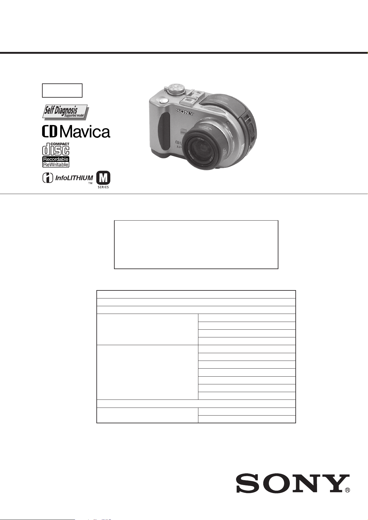
MVC-CD200/CD300
SERVICE MANUAL
Level 3
Ver 1.1 2001. 07
Photo : MVC-CD300
The information that is not described in this
Service Manual is described in the LEVEL 2
Service Manual.
When repairing, use this man ual together with
LEVEL 2 Service Manual.
US Model
Canadian Model
AEP Model
UK Model
E Model
Hong Kong Model
Australian Model
Chinese Model
Tourist Model
Korea Model
Japanese Model
This service manual contains information
for japanese model as well.
Contents of LEVEL 2 Service Manual
SERVICE NOTE
1. GENERAL
2. DISASSEMBLY
3. BLOCK DIAGRAMS
4. PRINTED WIRING BOARDS AND
SCHEMATIC DIAGRAMS
5. ADJUSTMENTS
6. REPAIR PARTS LIST
OVERALL
MODE CONTROL
LCD
POWER
CD-333 BOARD
CD-334 BOARD
TK-61 BOARD
CONTROL SWITCH BLOCK (ZK-503)
FS-83 BOARD
JK-208 BOARD
PK-58 BOARD
EXPLODED VIEWS
ELECTRICAL PARTS LIST
DIGITAL STILL CAMERA
Page 2
TABLE OF CONTENTS
2. DISASSEMBLY
2-16. MD-083 BOARD ··························································2-15
3. BLOCK DIAGRAMS
3-8.
CAMERA BLOCK DIAGRAM (1/2) (MVC-CD200)
3-9.
CAMERA BLOCK DIAGRAM (1/2) (MVC-CD300)
··3-15
··3-17
3-10. CAMERA BLOCK DIAGRAM (2/2)···························3-19
3-11. MD BLOCK DIAGRAM (1/3) ·····································3-21
3-12. MD BLOCK DIAGRAM (2/3) ·····································3-23
3-13. MD BLOCK DIAGRAM (3/3) ·····································3-25
4. PRINTED WIRING BOARDS AND
SCHEMATIC DIAGRAMS
4-2. PRINTED WIRING BOARDS AND
SCHEMATIC DIAGRAMS ··········································4-19
• SY-67 (LD, PEARL, VIDEO OUT, SH, 16M FLASH
MEMORY, 64M SDRAM, CLK GEN., CW, HI
CONTROL, AUDIO PROCESS, CONNECTOR,
DC/DC CONVERTER)
PRINTED WIRING BOARD ·······················4-19
• SY-67 (LD)(1/10)
SCHEMATIC DIAGRAM ····························4-23
• SY-67 (PEARL)(2/10)
SCHEMATIC DIAGRAM ····························4-25
• SY-67 (VIDEO OUT)(3/10)
SCHEMATIC DIAGRAM ····························4-27
• SY-67 (SH)(4/10)
SCHEMATIC DIAGRAM ····························4-29
• SY-67 (16M FLASH MEMORY, 64M SDRAM,
CLK GEN.)(5/10)
SCHEMATIC DIAGRAM ····························4-31
• SY-67 (CW)(6/10)
SCHEMATIC DIAGRAM ····························4-33
• SY-67 (HI CONTROL)(7/10)
SCHEMATIC DIAGRAM ····························4-35
• SY-67 (AUDIO PROCESS)(8/10)
SCHEMATIC DIAGRAM ····························4-37
• SY-67 (CONNECTOR)(9/10)
SCHEMATIC DIAGRAM ····························4-39
• SY-67 (DC/DC CONVERTER)(10/10)
SCHEMATIC DIAGRAM ····························4-41
• MD-083 (CD-RF PROCESS, SERVO, CD, DSP,
CD-R/RW GA, MD SYSTEM CONTROL,
EFM/ENC CONTROL)
PRINTED WIRING BOARD ·······················4-43
• MD-083 (CD-RF PROCESS)(1/5)
SCHEMATIC DIAGRAM ····························4-45
• MD-083 (SERVO)(2/5)
SCHEMATIC DIAGRAM ····························4-47
• MD-083 (CD DSP, CD-R/RW GA)(3/5)
SCHEMATIC DIAGRAM ····························4-49
• MD-083 (MD SYSTEM CONTROL)(4/5)
SCHEMATIC DIAGRAM ····························4-51
• MD-083 (EFM/ENC CONTROL)(5/5)
SCHEMATIC DIAGRAM ····························4-53
4-3. WAVEFORMS ······························································4-75
4-4. MOUNTED PARTS LOCATION ·································4-76
6. REPAIR PARTS LIST
6-1. EXPLODED VIEWS ······················································ 6-8
6-1-8.DDX-G2100 COMPLETE ASSEMBLY ························6-8
6-2. ELECTRICAL PARTS LIST ········································6-14
CAUTION
Use of controls or adjustments or performance
procedures other than those specified herein may
result in hazardous radiation exposure.
SAFETY-RELATED COMPONENT WARNING!!
COMPONENTS IDENTIFIED BY MARK 0 OR DOTTED LINE WITH
MARK 0 ON THE SCHEMATIC DIAGRAMS AND IN THE PARTS
LIST ARE CRITICAL TO SAFE OPERATION. REPLACE THESE
COMPONENTS WITH SONY PARTS WHOSE PART NUMBERS
APPEAR AS SHOWN IN THIS MANUAL OR IN SUPPLEMENTS
PUBLISHED BY SONY.
SAFETY CHECK-OUT
After correcting the original service problem, perform the following
safety checks before releasing the set to the customer.
1. Check the area of your repair for unsoldered or poorly-soldered
connections. Check the entire board surface for solder splashes
and bridges.
2. Check the interboard wiring to ensure that no wires are
"pinched" or contact high-wattage resistors.
3. Look for unauthorized replacement parts, particularly
transistors, that were installed during a previous repair . Point
them out to the customer and recommend their replacement.
ATTENTION AU COMPOSANT AYANT RAPPORT
À LA SÉCURITÉ!
LES COMPOSANTS IDENTIFÉS P AR UNE MARQUE 0 SUR LES
DIAGRAMMES SCHÉMA TIQUES ET LA LISTE DES PIÈCES SONT
CRITIQUES POUR LA SÉCURITÉ DE FONCTIONNEMENT. NE
REMPLACER CES COMPOSANTS QUE PAR DES PIÈSES SONY
DONT LES NUMÉROS SONT DONNÉS DANS CE MANUEL OU
DANS LES SUPPÉMENTS PUBLIÉS PAR SONY.
4. Look for parts which, through functioning, show obvious signs
of deterioration. Point them out to the customer and
recommend their replacement.
5. Check the B+ voltage to see it is at the values specified.
6. Flexible Circuit Board Repairing
• Keep the temperature of the soldering iron around 270˚C
during repairing.
• Do not touch the soldering iron on the same conductor of the
circuit board (within 3 times).
• Be careful not to apply force on the conductor when soldering
or unsoldering.
— 2 —
Page 3

SECTION 2
DISASSEMBLY
The following flow chart shows the disassembly procedure.
Refer to level 2
2-7. SY-67 board
2-8. Base unit (DDX-G2100 complete assembly)
NOTE: F ollo w the disassembly procedure in the numerical order given.
2-16.MD-083 BOARD
After performing “Disassembly” Section 2-7
SY-67 board of MVC-CD200/CD300
Service Manual Level 2 (page 2-7),
do the following.
2-16. MD-083 board
MD-083 board service position
MVC-CD200/CD300
1 Harness (FS-138) (2P)
(door lock plunger)
JK208
6 MD
heat sink
3 Precision
screw
(DIA 1.7 × 4)
2 Flexible board
(from spindle motor 18P)
SY67
M
083
D-
4 Dowel
5 Remove the MD heat sink
in the direction of the arrow A.
A
7
SY67
1 Precision
screw
(DIA 1.7 × 4)
JK208
3
8
-0
D
M
3 MD-083 board
B
M
D
-083
C
2 Remove the MD-083 board in the direction
of the arrow BC.
4
JK208
4 MD-083 board
2 Flexible board
(from optical device)
(32P)
SY67
3
8
-0
D
M
2-15
3 Ferrite core
1 Flexible
retainer
5
Page 4

[MD-083 BOARD SERVICE POSITION]
When using the CD-R/RW
drive unit. press S101 and S103.
(CD300)
CD-334 board
C
334
Lens block assembly
(CD200)
CD-333 board
D
C
333
Lens block assembly
Control switch block
(RL-503) (6P)
SY-67 board
Extension cable
(J-6082-487-A) (50P)
JK-208 board,
FP-361 flexible
-
D
-
board
FP-364 flexible
board (70P)
JK208
SY-67
-
D
M
083
MD-083 board
Flexible board
(from spindle motor 18P)
AC power
adaptor
1
18
AC IN
CPC-9 jig
(J-6082-393-C)
Adjustment remote
commander (RM-95)
Extension cable
(J-6082-374-A) (18P)
When using the CD-R/RW drive unit.
the dew sensor must be connected.
Harness (FS-140)
(2P) (dew sensor)
2-16E
Page 5

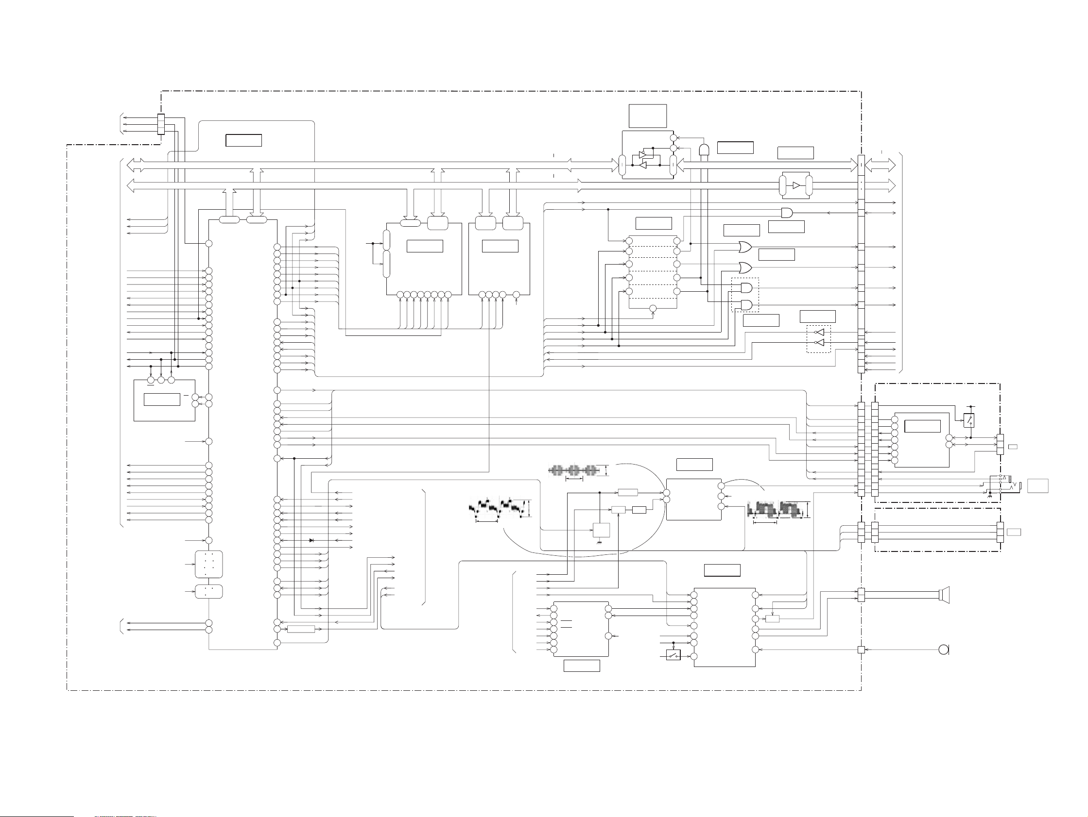
SECTION 3
BLOCK DIAGRAMS
MVC-CD200/CD300
3-8. CAMERA BLOCK DIAGRAM (1/2) (MVC-CD200)
IC101 8
33.3msec
IC101 5
33.3msec
IC101 4,6
3.475µsec
IC101 2
33.3msec
IC101 1,3
IC101 qf
3.475µsec
100µsec
54nsec
100µsec
1.0Vp-p
24.0Vp-p
7.5Vp-p
24.0Vp-p
7.5Vp-p
3.7Vp-p
CD-333 BOARD
(4-15)
IC101
CCD IMAGER
V OUT
V1A
V1B
V3A
V3B
H1
H2
RG
VSHT
CSUB
VDD
LENS UNIT
16
8
5
6
4
V2
2
3
1
V4
15
16
14
11
12
9
13
VL
IC101 qg,qh
54nsec
IRIS
METER
M
H
M001
FOCUS
MOTOR
M
M002
ZOOM
MOTOR
M
FOCUS
RESET
SENSOR
ZOOM
RESET
SENSOR
TEMP
Q102
BUFFER
Q101
SWITCH
3.6Vp-p
DRIVE-
DRIVE+
FOCUS A
FOCUS B
FOCUS B
FOCUS A
ZOOM A
ZOOM B
ZOOM B
ZOOM A
F SENS RST
F SENS VCC
Z SENS RST
Z SENS VCC
TEMP OUT
BIAS+
HALL+
HALL-
CCD OUT
V1A
V1B
V2
V3A
V3B
V4
H1
H2
RG
VSHT
VSUB CONT
CAM 15V
CAM -7.5V
CAM 15V
CAM -7.5V
CAM 3.1V
CAM 15V
CAM -7.5V
XCAM RST
XTG CS
(4-11)
IC303
Q301
CN301
13
12
DRIVE
IRIS
(1/2)
2
1
3
(4-12)
1
(4-12)
IC304
7
(2/4)
3
2
5
6
(1/4)
IC304
11
10
8
BIAS-
9
Q303
(4-11)
IC301
SHUTTER
23
DRIVE
2
IC302
ZOOM
MOTOR
DRIVE
(4-11)
5
7
FOCUS
17
MOTOR
DRIVE
19
24
1820
24
IN1,2
EN1,2
IN3,4
EN3,4
4
3
2
1
D 3.4V
CAP P 5V
1820
D 3.4V
42
75
1917
2321
17
16
15
14
6
7
20
19
Q302
21
( ) : Page No. shown in ( ) indicates the page to refer on the schematic diagram.
DVDD1
DVDD0
CLPDM
XSHD
XSHP
CLPOB
ADCLK
RST
SEN
24 27 33 40
S/H
36.818182MHz
36.5625MHz
29
31
34
10
12
77
5
6
8
19
21
22
24
25
23
16
17
15
14
27
CN704CN203
••
X202
XTAL OSC
X201
XTAL OSC
(4-14)
IC202
A/D CONVERTER
•
AGC
A/D
CONV.
D11
D0
SCLK
SDATA
Q201
XCAM SCK
CAM SO
MCK12
TG CLK
CN203 CN704
12 66
|
12
1
48
47
PAL/XNTSC
VSUB CNT
IC101
IRIS CONT1
18
IRIS CONT2
19
HALL REF
2
HALL GAIN
3
HALL OFFSET
4
PRELAMP AF ON
7
CNT C
9
SP VOL
8
PE DAC LEVEL1
12
PE DAC LEVEL2
13
DAC STBY
66
|
|
54
54
4242
32
32
38
38
30
30
45
45
46
46
35
35
33
33
AU CLK EN
(4-24)
VCC
11
VDD
10
DI
17
CLK
16
LD
15
39
40
41
43
44
46
47
9
12
13
42
45
14
2
33
IC304
IC303
IC304
119
1210
1513
1614
V2
V4
V1A
V1B
V3A
V3B
VSHT
RG
H1
H2
VH
VL
VDD3
RST
SEN
(4-12)
14
(4-11)
7
(4-12)
10
9
EN1
EN2
EN3
EN4
IC202 e;
IC201
TIMING
GENERATOR
9
IN1
10
IN2
11
12
13
IN3
14
15
IN4
16
124µsec
CLPOB
CLPDM
ADCLK
(4/4)
12
13
(2/2)
6
5
(3/4)
XSHP
XSHD
VDD1
VDD2
VDD4
VDD5
VDD3
MCK0
8
CAM 3.1V
1.0Vp-p
(4-14)
16
17
22
20
23
7
8
15
29
14
30
CKI
26
HDI
35
VDI
34
SCK
32
SSI
31
TH301
CAM 3.1V
CA HD
CA FD
XCAM SCK
CAM SO
XCAM RST
XEAGLE/
XGCAM CS
XCAM RST
XEAGLE/ XGCAM CS
XTG CS
IRIS CONT1
IRIS CONT2
HALL REF
HALL AD
HALL OFFSET
HALL GAIN
MSHUT ON
PE DIR0A
PE DIR0B
PE DIR1A
PE DIR1B
CCD TEMP
XFC RST SENS
XZM RST LED
XLENS RST LED
LENS TEMP AD
IRIS EN
DIR0B
PE EN0
PE EN1
17
13
30
23
22
21
20
16
43
46
29
31
34
10
12
5
6
8
19
21
22
24
25
23
16
17
15
28 28
26 26
18 18
14
27
SY-67 BOARD(1/3)
IC901 2
5.5Vp-p
IC901
CLOCK
GENERATOR
(4-32)
76
MODE CONTROL
(SEE PAGE
of LEVEL 2)
48MHz
CAM 3.1V
CAM SO
XCAM SCK
21nsec
X901
XTAL
OSC
IC901 qh
21nsec
IC901 9
USB CLK
16
MC CLK
11
92
AU CLK
TG CLK
4
61nsec
5.5Vp-p
4.5Vp-p
IC901 4
D 1.8V VCC2
4.3Vp-p
26.8nsec
(4-26)
IC302
64Mbit SDRAM
PRE LAMP AF ON
XRST SYS
PAL/XNTSC
EXT STRB ON
SYS V
CAM 3.1V
1
1427VCC
3
9
43
49
VCCQ
DQML
DQMH
20A0
14|
|
35
A13
2
DQ0
|
13
16 |
42
|
DQ15
53
15
39
16
WE-
17
CAS-
18
RAS-
19
CS-
38
CLK
3-6
STRB ON
STRB PHOTO ON
PHOTO TR OUT
Q311
IC301
CAMERA DSP,MEMORY CONTROL,
VIDEO ENCODER,OPD,OSD,HOST IF,
RES CONTROL,SG,JPEG,L-MODE,
AUDIO I/F,SHUTTER CONTROL,
STROB CONTROL
8
AD IN 11
|
12
|
20
AD IN 00
9
47
83
101
VCC3CAM 3.1V
117
130
141
192
30
71
106
145
196
223
48
MCK12
5
CA HD
6
CA FD
202
VSUB CONT
114
AQ00
|
|
96
AQ13
144
DQ00
|
126
DQ15
125
QDML
124
QDMH
122
XWE
121
XCAS
120
XRAS
118
XCSO
94
QCLK
187
XFC RST SENS
148
XZM RST SENS
149
XFC RST SENS
150
XLENS RST LED
147
IRIS EN
188
PE EN0
189
PE DIR0A
190
PE DIR0B
193
PE EN1
194
PE DIR1A
195
PE DIR1B
198
M SHUT ON
59
XRST SYS
161
PE DAC LEVEL1
172
PE DAC LEVEL2
179
PAL/XNTSC
200
EXT STRB ON
199
STRB ON
158
STRB PHOTO ON
203
STRB AD
162
PY0
168
CR0
165
CB0
(4-25)
NT VD0
IRQ IMG
IRQ JPG
IRQ AUDIO
MC XCS2
MC XCS6
MC HCLK
PEARL FLD
MC DRAK0
MC DREQ0
XPWAD
XPWDA
LCD VD
WRLX
WRHX
9375D00
|
|
16
D15
38
A01
|
|
14
23
A14
184
64
63
66
41
40
72
183
69
67
39
RDX
42
43
AUCLK
218
ACLK
(IC901)
207
SIA
208
SOA
209
LRCK
210
SCLK
211
ADCK
212
213
185
182
HD
173
YO
176
CO
SYS V
IRQIMG
IRQJPG
IRQAUDIO
MC XCS2
MC XCS6
AU LRCK
MC HCLK
PEARLFLD
MC DRAK0
MC DREQ0
MC XRD
MC XWE0
MC XWE1
CAM SO
XCAM SCK
XCAM RST
XTG CS
XEAGLE/XGCAM CS
HALL AD
LENS TEMP AD
AU CLK EN
DAC STBY
CCD TEMP
AU SDTO
AU SDTI
AU LRCK
AU SCLK
AU MCLK
AU XPWAD
AU XPWDA
Y OUT
C OUT
CNT C
SP VOL
CAMERA(2)
(SEE PAGE
3-19)
CAMERA(2)
(SEE PAGE
3-19)
Q305 B
Q305
BUFFER
BUFFER
Q306
0.5Vp-p
H
Q307
BUFFER
CN707
PANEL V
5
HD0
4
PANEL Y
9
PANEL R-Y
8
PANEL B-Y
7
LCD
(PK-58)
(SEE PAGE 3-7
of LEVEL 2)
3-15 3-16
Q306 B
0.2Vp-p
H
Page 6

MVC-CD200/CD300
3-9. CAMERA BLOCK DIAGRAM (1/2) (MVC-CD300)
IC401 q;
124µsec
IC401 5
33.3msec
IC401 4,6
124µsec
2µsec
IC401 2
33.3msec
IC401 1,3
2µsec
124µsec
IC401 qs
54nsec
1.0Vp-p
22.0Vp-p
7.5Vp-p
22.0Vp-p
7.5Vp-p
3.7Vp-p
CD-334 BOARD
(4-16)
IC401
CCD IMAGER
V OUT
V1A
V1B
V3A
V3B
RG
VSHT
CSUB
VDD
IC401 qd,qf
LENS UNIT
16
V2
V4
H1
H2
VL
54nsec
IRIS
METER
M
M001
FOCUS
MOTOR
M
M002
ZOOM
MOTOR
M
FOCUS
RESET
SENSOR
ZOOM
RESET
SENSOR
Q402
10
BUFFER
5
6
4
2
3
1
14
13
12
16
Q401
17
SWITCH
11
18
CCD OUT
V1A
V1B
V2
V3A
V3B
V4
H1
H2
RG
VSHT
VSUB CONT
CAM 15V
CAM -7.5V
CAM 15V
CAM -7.5V
CAM 5V
CAM 15V
CAM -7.5V
XCAM RST
XTG CS
4.7Vp-p
IC202 qh
54nsec
CN302
IRIS B
3
IRIS B
5
IRIS A
4
IRIS A
2
FOCUS A
6
FOCUS B
7
FOCUS B
5
FOCUS A
8
D 3.4V
CAP P 5V
ZOOM A
10
ZOOM B
9
ZOOM B
12
ZOOM A
11
F SENS RST
15
F SENS VCC
14
Z SENS RST
3
Z SENS VCC
2
Q302
TEMP OUT
TEMP
CN303
D 3.4V
42
75
1917
2321
1820
IC302
(4-11)
ZOOM
MOTOR
DRIVE
21
IC301
4
33
IRIS
MOTOR
2
DRIVE
5
7
FOCUS
MOTOR
17
DRIVE
19
24
1820
24
IN1,2
EN1,2
IN3,4
EN3,4
( ) : Page No. shown in ( ) indicates the page to refer on the schematic diagram.
A/D
CONV.
Q201
CN203 rs
D11
D0
SCLK
SDATA
12
XCAM SCK
CAM SO
MCK12
PAL/XNTSC
TG CLK
VSUB CNT
3.2Vp-p
CN203 CN704
54nsec
12 66
|
1
48
47
IC101
PRELAMP AF ON
7
CNT C
9
SP VOL
8
PE DAC LEVEL1
12
PE DAC LEVEL2
13
DAC STBY
IC103
12
IRIS
MOTOR
13
PRE-
DRIVE
(4-24)
1
VD
VCC
VDD
CLK
(4-24)
DI
LD
66
|
|
54
54
4242
32
32
38
38
30
30
45
45
46
46
35
35
33
33
AU CLK EN
11
10
17
16
15
CAM SI
6
CAM SO
5
XCAM SCK
4
XTG CS
3
XBEAR RST
9
8
DVDD1
DVDD0
CLPDM
XSHD
XSHP
CLPOB
ADCLK
RST
SEN
24 27 33 40
S/H
36.818182MHz
XTAL OSC
36.5625MHz
XTAL OSC
CN704CN203
29
31
34
IC202
A/D CONVERTER
••
X202
X201
(4-14)
•
AGC
IC202 e;
CAM 3.1V
XSHP
VDD3
MCK0
1.0Vp-p
(4-14)
16
XSHD
17
22
20
23
VDD1
7
VDD2
8
15
VDD4
29
VDD5
14
30
CKI
26
HDI
35
VDI
34
SCK
32
SSI
31
CAM 3.1V
CA HD
CA FD
XCAM SCK
CAM SO
XCAM RST
XEAGLE/
XGCAM CS
XCAM RST
XEAGLE/ XGCAM CS
XTG CS
17
13
30
23
22
21
20
16
43
46
29
31
34
124µsec
IC201
TIMING
GENERATOR
V2
39
V4
40
41
43
44
46
47
9
12
13
42
45
14
2
33
CLPOB
V1A
V1B
CLPDM
ADCLK
V3A
V3B
VSHT
RG
H1
H2
VH
VL
VDD3
RST
SEN
3.4Vp-p
9
IN1
10
EN1
IN2
11
EN2
12
13
IN3
14
EN3
15
IN4
16
EN4
MSHUT ON
PE DIR0A
PE DIR0B
IRIS EN
DIR0B
PE EN0
19
19
21
21
22
22
24
24
25
25
23
23
IC102
119
1210
1513
1614
TH301
PE DIR1A
PE DIR1B
CCD TEMP
XFC RST SENS
XZM RST LED
XLENS RST LED
LENS TEMP AD
PE EN1
16
17
15
28 28
26 26
18 18
14
27
16
17
15
14
27
CN704CN203
IC104
IC105
VD PULSE
GENERATOR
(4-24)
SYS V
M SHUT ON
SY-67 BOARD(1/3)
IC901 2
5.5Vp-p
IC901
CLOCK
GENERATOR
(4-32)
76
(SEE PAGE
of LEVEL 2)
PLL 12
(IC301)
48MHz
CAM 3.1V
CAM SO
XCAM SCK
21nsec
X901
XTAL
OSC
MODE CONTROL
3-6
IC901 qh
21nsec
IC901 9
USB CLK
16
MC CLK
11
92
AU CLK
TG CLK
4
61nsec
5.5Vp-p
4.5Vp-p
IC901 4
D 1.8V VCC2
4.3Vp-p
26.8nsec
(IC103)
(4-26)
IC302
64Mbit SDRAM
DQML
DQMH
20A0
14|
|
35
A13
2
DQ0
|
13
16 |
42
|
DQ15
53
15
39
16
WE-
17
CAS-
18
RAS-
19
CS-
38
CLK
PRE LAMP AF ON
XRST SYS
PAL/XNTSC
EXT STRB ON
STRB ON
STRB PHOTO ON
PHOTO TR OUT
SYS V
CAM 3.1V
1
1427VCC
3
9
43
49
Q311
VCCQ
IC301
CAMERA DSP,MEMORY CONTROL,
VIDEO ENCODER,OPD,OSD,HOST IF,
RES CONTROL,SG,JPEG,L-MODE,
AUDIO I/F,SHUTTER CONTROL,
STROB CONTROL
8
AD IN 11
|
12
|
20
AD IN 00
9
47
83
101
VCC3CAM 3.1V
117
130
141
192
30
71
106
145
196
223
48
MCK12
74
PLL12PLL12
5
CA HD
6
CA FD
202
VSUB CONT
114
AQ00
|
|
96
AQ13
DQ00
144
|
DQ15
126
125
QDML
124
QDMH
122
XWE
121
XCAS
120
XRAS
118
XCSO
94
QCLK
187
XFC RST SENS
148
XZM RST SENS
149
XFC RST SENS
150
XLENS RST LED
147
IRIS EN
188
PE EN0
189
PE DIR0A
190
PE DIR0B
193
PE EN1
194
PE DIR1A
195
PE DIR1B
198
M SHUT ON
59
XRST SYS
161
PE DAC LEVEL1
172
PE DAC LEVEL2
179
PAL/XNTSC
200
EXT STRB ON
199
STRB ON
158
STRB PHOTO ON
203
STRB AD
162
PY0
168
CR0
165
CB0
(4-25)
NT VD0
IRQ IMG
IRQ JPG
IRQ AUDIO
MC XCS2
MC XCS6
MC HCLK
PEARL FLD
MC DRAK0
MC DREQ0
XPWAD
XPWDA
LCD VD
WRHX
WRLX
9375D00
16
|
|
D15
38
A01
14
|
|
23
A14
184
64
63
66
41
40
72
183
69
67
39
RDX
42
43
AUCLK
218
ACLK
(IC901)
207
SIA
208
SOA
209
LRCK
210
SCLK
211
ADCK
212
213
185
182
HD
173
YO
176
CO
SYS V
IRQIMG
IRQJPG
IRQAUDIO
MC XCS2
MC XCS6
AU LRCK
MC HCLK
PEARLFLD
MC DRAK0
MC DREQ0
MC XRD
MC XWE0
MC XWE1
CAM SI
CAM SO
CAM SCK
XCAM RST
XTG CS
XEAGLE CS
HALL AD
LENS TEMP AD
AU CLK EN
DAC STBY
CCD TEMP
XBEAR RST
AU SDTO
AU SDTI
AU LRCK
AU SCLK
AU MCLK
AU XPWAD
AU XPWDA
Y OUT
C OUT
CNT C
SP VOL
CAMERA(2)
(SEE PAGE
3-19)
CAMERA(2)
(SEE PAGE
3-19)
Q305 B
0.5Vp-p
H
Q305
BUFFER
BUFFER
BUFFER
Q306
Q307
CN707
PANEL V
5
HD0
4
PANEL Y
9
PANEL R-Y
8
PANEL B-Y
7
LCD
(PK-58)
(SEE PAGE 3-7
of LEVEL 2)
3-17 3-18
Q306 B
0.2Vp-p
H
Page 7
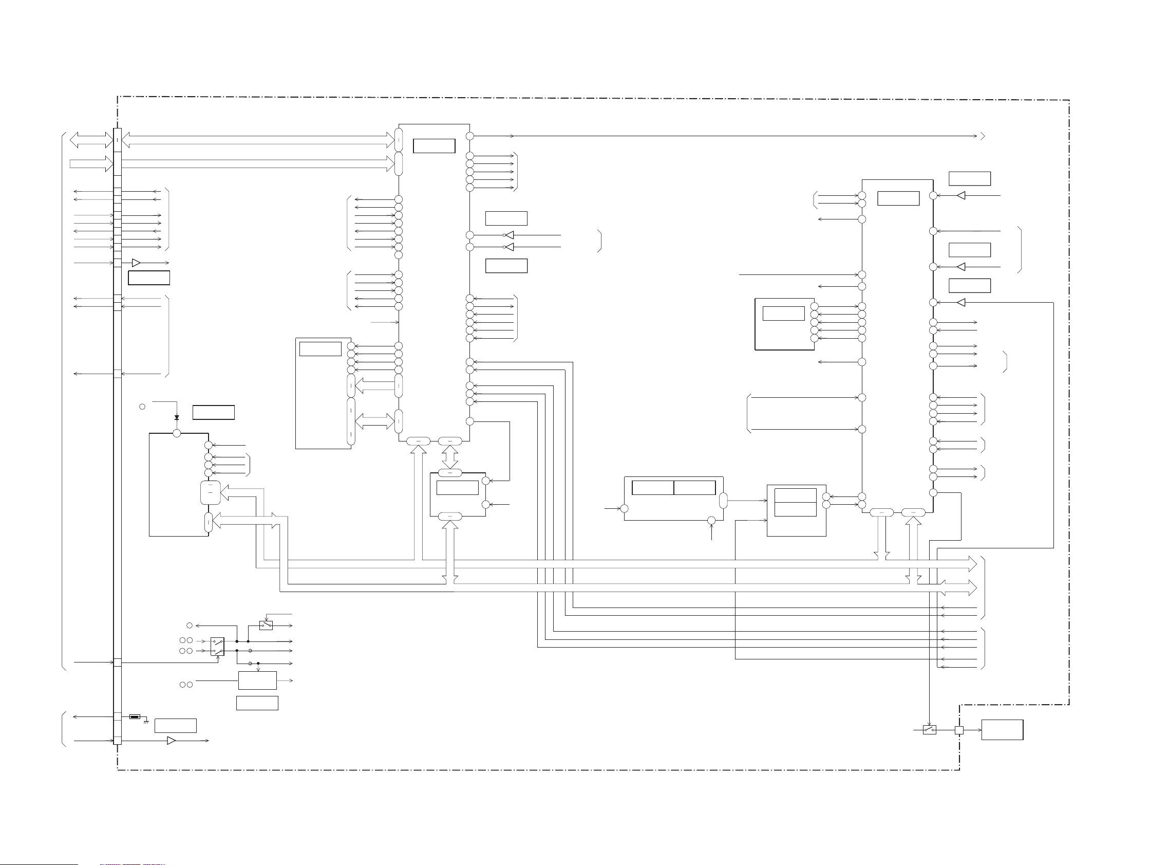
MVC-CD200/CD300
3-10.CAMERA BLOCK DIAGRAM (2/2)
SY-67 BOARD(2/3)
94
9
10
11
12
101
105
166
169
185
196
198
199
179
173
174
(4-32)
1
117
CS
6
27
RST
134
90
31
33
115
112
206
207
26
29
161
7462 100
170116 190
201
88
8430
182
159
18
21
IC501
20
57-80
A1-A20 D0-D15
XCS LCD DAC
SYS V
IRQ IMG
IRQ JPG
IRQ AUDIO
MC XCS2
MC XCS6
AU LRCK
MC HCLK
PEAL FLD
MC DRAK0
MC DREQ0
MC DREQ1
CAM SI
CAM SO
XCAM SCK
XEEPROM CS
XEEPROM RESET
UCLK
XCAM RESET
XTG CS
XCAM RESET
XTG CS
XEAGLE/XGCAM CS
HALL AD
LENS TEMP AD
DAC ENB
DAC STBY
EXTAL
483622
VCCQ
139
VCC
(4-29)
MC CAM
SH DSP
16
35-53
MC RDXWR
MC XCS3
MC CKE
MC XRAS
MC XCAS
MC XRD
MC XWE0
MC XWE1
MC XCS0
DRAGON RST
MC DACK1
XMD POWER SAVE
MC DREQ
IRQ FDC/CW
MC XCS4
MC XCS5
MC XCLK
USB D+PULLUP
USB TXENL
USB XVDATA
USB D+ IN
USB D– IN
USB SUSPND
USB D– OUT
USB D+ OUT
USB VBUS
HI SO
HI SI
XHI SCK
XMC CS
NMI XMC NMI
XMC HELP
XRESETP
SELF TIMER SELF TIMER
AU HGL SEL
XAU SP MUTE
XAU LINE MUTE
MS BS
MS DIO
MS SCLK
PAL/XNTSC
ACCESS LED
V OUT ON
3-7
(SEE PAGE
of LEVEL 2)
CAMERA(1)
(SEE PAGE
3-16(MVC-CD200),
3-18(MVC-CD300))
16
(PK-58)
LCD
POWER
XCS PANEL D/A
CAM SO
XCAM SCK
16
14
MC XRD
MC XWE0
MC XWE1
SYS V
IRQIMG
IRQJPG
IRQAUDIO
MC XCS2
MC XCS6
AU LRCK
MC HCLK
PEARLFLD
MC DRAK0
MC DREQ0
CAM SI
CAM SO
XCAM SCK
CN707
17
18
19
234
SCK DI DO
IC505
EEPROM
(16KBIT)
USB CLK
(IC901)
AU CLK EN
XBEAR RST
XCAM RST
XTG CS
XEAGLE CS
HALL AD
LENS TEMP AD
CCD TEMP
DAC STBY
MC CLK
(IC901)
CAM 3.1V
D 1.8V
CAM DD ON
LCD DD ON
( ) : Page No. shown in ( ) indicates the page to refer on the schematic diagram.
MC D00
VCC
CAM 3.1V
0.5Vp-p
Y OUT
C OUT
CNT C
SP VOL
AU SDTI
AU SDTO
AU LRCK
AU SCLK
MC D15
MC A01
MC A03
DRAGON RST
MC HCLK
MC XRD
MC XWE0
MC XCS4
MC XCS5
MC DREQ1
IRQ FDC/CW
XMD POWER SAVE
IC201 8
8
13
14
11
10
12
DATA BUS
ADDRESS BUS
16
14
16
2-13
20-35
1
14
96
102
110
111
113
91
92
93
99
23
120
32
199
13
103
104
169
14
187
186
146
145
191
147
148
189
178
171
172
177
106
200
121
122
124
123
193
194
192
210
USB DET
AV JACK IN
8
MS BS
MS DIO
MS SCLK
15
LED DRIVE
Q501
25
CAM 3.1V
XRST FLASH
HI SO
HI SI
XHI SCK
XMC CS
XMC HELP
XRST SYS
VCC
27
3
9
VCCQ
49
43
DQML
15 16 17 18 19 37 38 39
MC XWEO
AV JACK IN
USB JUCK IN
PAL/XNTSC
ACCESS LED
BEEP ON
BEEP
42-53
A0-A13 DQ0-DQ15
IC504
SDRAM
64MBIT
WE-
CAS-
RAS-
CS-
MC RDXWR
MC XCAS
MC XRAS
MC XCS3
MC CKE
MODE
(SEE PAGE 3-6
of LEVEL 2)
CKE
CLK
MC HCLK
CONTROL
DQMU
MC XWE1
20
1-9,
16-25,
48
IC503
(4-31)(4-31)
FLASH ROM
RESET-OECE
WE-
11
12 26 28 37
MC XWE1
XRST FLASH
MC XCSO
IC201 1
H
CAMERA(1)
(SEE PAGE
3-16(MVC-CD200),
3-18(MVC-CD300))
16MBIT
DQ0-DQ15A1-A20
MC XRD
29-36
38-45
AU XPWAD
AU XPWDA
AU MCLK
MC DACK1
H
SDTI
SDTO
PW AD
PW DA
MCLK
LRCK
SCLK
IC251
AUDIO AD/DA CONV.
A OUT L
A IN L
MCA1-MCA3
0.4Vp-p
Q301
TRAP
FREQ.
SW
VDD
(4-37)
159
3
5
16
3
(4-33)
Q309,310
IC154
IC155
9
2
14
D6
3
D1
6
D2
12
D3
11
D4
Q303
BUFFER
Q304,308
ATT
EVR
IC158
DELAY
CK
9
(4-33)
19
X OE
1
11
18
15
Q6
2
Q1
7
Q2
12
Q3
10
Q4
IC201
VIDEO AMP
8
Y IN
1
C IN
POWER SAVE
21
V OUT
(4-33)
4
IC156
(4-33)
IC153
214
2
4
1
2
7
1
6
3
5
IC157
(4-28)
3
5
VCC
6
V OUT ON
A 3.4V
IC201 3
IC152
(4-33)
(4-33)
H
IC158
5
9
12
2
1
IC160
(4-34)
(4-33)
4
2.1Vp-p
6
8
11
IC151
53
71
DRAGON RST
USB D+PULLUP
USB TXENL
USB XVDATA
USB D+ IN
USB D– IN
USB SUSPND
USB D– OUT
USB D+ OUT
USB DET
AV JACK IN
MC DACK1
(4-33)
CN701
16
3
CN709
CN707
46
31
HA0-HA2
19
22
18
HRESET
30
DACK
23
IOR
24
IOW
26
16
17
DREQ
29
HINT
21
XMD POWER SAVE
20
MPXO IF
5
DECEFM
2
FM DT
1
16
12
19
9
20
8
21
7
22
6
23
5
17
10
18
11
7
21
8
20
10
18
12
16
26
27
25
26
24
25
HDB0
MDB15
16
HCS1
HCS0
CN101
CN301
3
MD BLOCK
(MD-083)
(SEE PAGE
JK-208 BOARD(1/2)
2
3
IC101
4
5
6
12
(4-61)
13
(SEE PAGE
4-67)
3-21)
D 3.4V
Q103
MS SCLK
MS BS
MS DIO
D+
11
D-
10
V OUT
A OUT
USB
I/F
PK-58 BOARD(1/3)
D+
3
D-
CN102
2
USB
VCC
1
J102
A/V OUT
(MONO)
14
CN301
15
CPC
FOR CHECK
16
(4-38)
IC252
A 3.4V
A 3.4V
A 4.9V
CAM P 5V
BEEP
BEEP ON
Q253
11
16
19
25
10
21
44
48
LINE/SPEAKER AMP
BEEP IN
VOL CTL
PB IN
REC OUT
XBEEP MUTE
VCC
VCCH
SP VCC
LPF SEL
XAUDIO MUTE
LINE OUT
SP OUT+
SP OUT-
MIC IN
SP +
MIC SIG
1
SP -
2
CN706
1
CN711
20
15
46
40
AU HGL SEL
XAU LINE MUTE
XAU SP MUTE
Q251,252
MUTE
1
3
SP+
SP901
SP-
SPEAKER
MIC901
MIC UNIT
3-19 3-20
Page 8
MVC-CD200/CD300
3-11.MD BLOCK DIAGRAM (1/3)
MD-083 BOARD(1/3)
31
46
19
22
18
29
21
17
16
23
24
26
30
2
1
5
CN404
HDREQ
HINTRQ
XHCS0
XHCS1
XHDAK
XHIOR
XHIOW
IC419
DECEFM
FMDT
BACKUP VCC
(CN404 48 )
XCDR RSTO
41
DATA
ADDRESS
(IC414)
(IC207,404,420)
(4-53)
(IC013)
(SEE PAGE 3-23)
D405
(4-52)
8
XCE1
CE2
X0E
RX/W
CAMERA(2)
(SY-67)
(SEE PAGE
3-20)
HDB0-HDB15
16
HA0-HA2
3
DREQ
HINT
HCS0
HCS1
DACK
IOR
IOW
HRESET
DECEFM
FMDT
MPXO IF
( ) : Page No. shown in ( ) indicates the page to refer on the schematic diagram.
IC401
SRAM
30
6
32
5
14
10 20
31
21
29
XCSSRAM
SRAM CE
XRD
XWR
8
(IC207)
(SEE PAGE 3-23)
(IC404)
A0-A16
17
D8-D15
(4-53)
IC408
4MBYTE
BUFFER
DRAW
(CN404)
(IC404)
84HD0-HD15
102
72HA0-HA2
74
71
82
76
70
69
77
80
81
75
28
5
4
26
25
128
2
127
3
114
126
103
111
15
(4-54)
IC414
ATAPI
CD-R
ENC/DEC
EFM ENC
CONTROL
8
24
88
11
16
3
HDREQ
HINTRQ
XHCS0
XHCS1
XHDAK
XHIOR
XHIOW
XCLRST
XRD
XWR
XCLDINT
XCLHINT
4.6V
XCAS
23
XMOE
22
XRAS
7
XWE
6
BA0-BA11
8
12
21
2
BD0-BD7
5
8
24
27
IC407
BUS
SW
9
8
17
19
2
D8-D15
42
54
47
40
41
33
45
29
61
58
65
57
60
59
55
56
64
62
63
6
(4-53)
ENCEFM
ATSY
CLVM
ENSY
SOCK
WLDON
IC413
IC410
C2PO
EXCK
GRSCOR
SBSO
SQSY
WFCK
FMCK
FMDT
MDATA
LRCK
BCLK
XCSCL
19
1
(4-53)
42
(4-53)
XRD
(IC207)
(SEE PAGE 3-23)
24
(IC201)
(SEE PAGE 3-25)
(IC404)
C34MV
C17MV
(IC207)
(IC207)
(IC013)
(SEE PAGE
3-24)
(SEE PAGE 3-23)
TE
3
IC200 IC208
TSHOCK
DETECT
(4-49)
TSNSCMP(IC019)
(SEE PAGE 3-24)
(IC207)
(SEE PAGE 3-23)
(IC414)
1
7
3
NMI
TSHOOK
FSHOOK
IC406
EEPROM
(4-52)
XCLDINT
XCLHINT
IC423
IC400
(CN404)
(IC401)
OR,
LAICH
(4-51)
(Q407)
(IC414)
ENCEFM
MD BLOCK(2/3)
(SEE PAGE
3-23)
(4-51)
100
3
67
1
92
55
2
54
21
96
95
56
19
6
73
12
71
72
LDEN
SLFG
SP ON
XRFRST
WAPCFUP
SENS
SNSCLK
XMRST
C2PO
XGAINT
XSQINT
XRD
XWR
DOOR LOCK
ADDRESS
IC403
4
1
IC418
2
4
IC402
4
2
ASTY
C17MV
(4-51)
TZC
(4-51)
LMT
(CN001)
(IC207)
(IC003)
(IC013)
(IC012)
(IC201)
(SEE PAGE
3-25)
(IC207)
(SEE PAGE
3-23)
(IC207,401,
(SEE PAGE
3-23)
(IC414)
(IC207)
(SEE PAGE
3-23)
(IC013)
(SEE PAGE
(SEE PAGE
3-24)
3-23)
(SEE PAGE 3-26)
(SEE PAGE
3-24)
407,414)
EJECT
XCDR RSTO
SRAM CE
XPD
E2DI
E2DO
3
E2RST
6
XE2CK
2
XE2CS
1
XCLRST
6
5
XCLR
76
62
89
63
16
974
10
99
14
74
75
91
94
A0-A19
(4-51)
IC404
SYSTEM
CONTROL
(MD)
5
8
30
32
53
23
820
D8-D15
MODE CONTROL
(SEE PAGE
3-6
of LEVEL 2)
(SY-67)
XMD POWER SAVE
TH OUT
XLID OPEN
DATA
FM CK
CN405
FM DT
MDATA
LRCK
BCLK
FSHOCK
LMT
1
CW 3.4V (CN404 15 )
D 3.4V (CN404 9 10 )
D 4.6V (CN404 11 12 )
20
CW UNREG
(CN404 13 14 )
TH401
3
IC422
47
14
EJECT
Q403,404,418
(4-53)
(IC404,CN001)
Q407,409
FB410
FB405
DC/DC
CONVERTER
IC425
Q411,417
XPD(IC404)
DSP 3.4V
3.4V
4.6V
4.6V-2
POWER 5V
(4-53)
Q412,416
3.4V
MD BLOCK(2/3)
(SEE PAGE
3-23)
MD BLOCK(3/3)
(SEE PAGE
3-25)
PL902
VCC
DOOR LOCK
PLUNGER
16
3-21 3-22
Page 9

MVC-CD200/CD300
3-12.MD BLOCK DIAGRAM (2/3)
MD-083 BOARD(2/3)
ENCEFM
49
(4-50)
IC207
ATSY
CLVM
ENSY
SOCK
WLDON
X202
34.574MHz
C34MV
C17MV
LOCKCD
MIRRO
MNTO
MNT1
MNT2
MNT3
SQCK
SQSO
SQSY
XTSL
XCSSRAM
XCDR RSTO
XGAINT
XRD
XSQINT
XWR
NMI
C33M
3.4V
FM CK
FM DT
(1/3)
ADDRESS
DATA
CD-R/RW
53
GA
52
50
51
48
42
41
43
46
128
125
121
122
123
124
118
119
120
131
69
116
133
87
134
88
132
44
74
86 101
20 8
A0-A9 D8-D15
16
MD BLOCK
(SEE PAGE
3-22)
(SEE PAGE
3-22)
(SEE PAGE 3-21)
(SEE PAGE3-22)
(SEE PAGE 3-22)
(SEE PAGE 3-25)
(SEE PAGE
(1/3)
(IC414)
(SEE PAGE
3-21)
(IC013,414)
(IC414,404)
(IC201)
(SEE PAGE
3-25)
(IC401)
(IC404)
(IC404)
(IC404)
(IC201)
MD BLOCK
3-22)
( ) : Page No. shown in ( ) indicates the page to refer on the schematic diagram.
EQEFM
33
ODPLS
34
OSCON
36
WAPCRW
32
SPBRK
2
SPREV
57
ACTEN
63
XRW
3
ASMP
26
AGCON
22
ATFG
10
MIRR
15
MPXO
113
MSMP
24
RAPC
31
RC
16
RECD1
21
RECD2
20
RFGUP
23
RSMP
27
RZC
14
SSMP
25
TZC
13
142
WAPC
29
WAMP
28
DFCT
130
XTOK
17
FOK
129
FMCK
11
FMDT
12
Q203
144
MDPGA
60
MDSGA
61
SOFF
59
SPLHLD
143
VREF-
111
VREF+
115
XSDLTRF
5
SDLTDA
6
XSDLTDSP
4
SWDT
8
SDCK
7
SLFG
58
SPFG
56
94
XDFCT2
DFCT
DFCT2
(SEE PAGE 3-25)
(SEE PAGE 3-25)
(CN001)
(IC012)
(IC003)
(Q004)
(IC013)
(IC013,204)
(SEE PAGE
3-25)
(IC014)
(SEE PAGE
3-25,26)
(IC013,014)
(IC019)
(IC201)
(IC404)
(SEE PAGE
3-22)
(SEE PAGE 3-26)
(SEE PAGE 3-21)
(4-50)
IC209
1
2
Q204
(SEE PAGE 3-25)
(SEE PAGE 3-22)
(SEE PAGE 3-26)
(SEE PAGE 3-25)
(SEE PAGE
(SEE PAGE
4
3-25)
3-21)
(SEE PAGE
(SEE PAGE
(CN404)
(IC207)
(IC207)
(IC204,207)
(IC207,404)
(IC207,014)
(IC201,207)
(IC201,207)
(CN404)
(IC201)
3-25)
(IC207,014)
3-25)
(IC404)
(SEE PAGE
3-22)
FM DT
C34MV
ASMP
AGCON
ATFG
MIRR
MPXO
MSMP
RAPC
RC
RECD1
RFGUP
RSMP
RZC
SSMP
WAPC
WAMP
DFCT2
TZC
RECD2
DFCT
FMCK
FMDT
FOK
DECEFM
EQRF
MPP
RRF
XSDLTRF
SWDT
SDCK
XRFRST
VWDC
(4-46)
IC013
49
CD-R/RW
57
RF PROCESS
36
39
47
85
55
61
45
44
35
58
52
56
60
59
46
42
43
46
37
38
48
54
80
11
77
66
65
64
63
6
VRDC
10
8
9
7
5
PD-A
91
PD-H
99
FPDIN
4
TE
TE
13
FE
14
TEO
83
VC
15
VREF+
3
XTOK
41
DIAG
84 13
TE,FE
SLMOVE
SL FG
SP FG
SDCK
SWDT
RFAC
4.6V
4.6V-2
IC012
SW
(4-46)
(IC200)
(IC014)
(SEE PAGE
3-25,26)
(IC014,201,207)
(SEE PAGE
3-25,26)
MD BLOCK(3/3)
(SEE PAGE
3-25)
WAPCRW
WAPCFUP
(SEE PAGE3-22)
(IC207)
(IC404)
(SEE PAGE
(SEE PAGE 3-26)
(SEE PAGE 3-25)
(SEE PAGE 3-22)
3-22)
(IC014)
(IC207)
(IC014)
(IC208)
(SEE PAGE
3-22)
HAVCOS
LDLMT
VWDC2
DIAG
SLVOS
SDLTDA
SEOS
SNSCMP
TSNSCMP
SLMOVE
(IC404)
(IC207)
(IC014)
DSP3.4V
BASE UNIT(1/2)
20
21
31
32
30
29
27
26
25
18
7
10
13
16
11
12
19
(DDX-G2100)
LD
DRIVE
PD
IC
FRONT
MONITOR
OPTICAL
DEVICE
LASER
DIODE
CN001
LDD5V
4.6V
W/XR
IC002
2
EJECT
LDEN
1
ODPLS
OSCON
VWDC
VWDC2
VRDC
LDLMT
VREF+
D002
SW
IC007
4.6V
OFFSET
IC019
D/A
CONV.
(EVR)
(4-48)
AMP
HAVCOS
4.6V
12
2
19
6
17
16
15
5
8
7
9
(4-45)
ENBL(IC404)
4
ODON
VWDC1
VWDC2
VRDC
A-H
(4-45)
VCC
VC
FPDON
3-23 3-24
Page 10

MVC-CD200/CD300
3-13.MD BLOCK DIAGRAM (3/3)
MD-083 BOARD(3/3)
(4-49)
MD BLOCK
(1/3)
(SEE PAGE
3-22)
(SEE PAGE
(SEE PAGE
(SEE PAGE
(SEE PAGE
MD BLOCK
(1/3)
(SEE PAGE
3-22)
(IC207)
3-23)
(IC
3-21)
3-22)
3-21)
(IC404,
(SEE PAGE
3-21,22)
(IC404)
(IC414)
414)
MDATA
LRCK
BCLK
DSP3.4V
LOCKCD
MIRRO
MNTO
MNT1
MNT2
MNT3
SQCK
SQSO
XTSL
414)
SQSY
SENS
SNSCLK
XMRST
EXCK
GRSCOR
SBSO
WFCK
C2PO
LMT
FSHOCK
24
IC201
22
CD DSP
26
AUDIO DAC
100
86
42
41
40
39
58
57
44
54
78
79
60
56
90
55
53
37
( ) : Page No. shown in ( ) indicates the page to refer on the schematic diagram.
TE,FE
SLMOVE
(SEE PAGE
(IC207)
(IC013)
(SEE PAGE
(IC014)
(IC207)
(SEE PAGE
SL FG
SP FG
RFAC
SDCK
SWDT
XDFCT2
(4-49)
3-23)
3-23)
3-23)
(IC207)
(SEE PAGE
3-23)
(IC207)
(SEE PAGE
3-23)
(SEE PAGE
3-23)
SOFF
(SEE PAGE
(SEE PAGE
SAO
SOFF
(IC207)
IC015
(4-48)
(IC207)
(SEE PAGE
3-23)
(IC013)
(IC019)
SW
3-23)
3-24)
Q006
IC011
FAO
TAO
FEIN
TEO
SLVOS
SLMOVE
(4-47)
SWDT
SDCK
XSDLTRF
DFCT2
MDPGA
MDSGA
SPLHLD
FSHOCK
FORCUS
11
SERVO
TRACKING
9
SERVO
73
FE AMP
TEIN
75
TE AMP
71
SLED
39
SERVO
78
7
72
70
SAMO
40
(4-48)
IC014
43
44
42
8
3
SE
SLED
4
POSITION
AMP
5
RECD2
69
XTOK
74
VC
53
VREF+
52
VREF-
51
SEOS
6
68
67
SPINDLE
63
SERVO
SHOCK
SENSOR
16
EC
55
SENS
15
SNSCMP
14
MD BLOCK(2/3)
(SEE PAGE
3-23)
RFAC
12
FAO
94
TAO
93
FEIN
2
TEIN
120
SWDT
81
SDCK
83
XSDLTDSP
82
SAO
92
14
15
87
88
119
118
80
1
3
98
70
71
45
IC204
SW
DFCT
FOK
MPP
RRF
XTOK
SE (IC207,013)
VC
MDPCD
X200
33.868MHz
C33M
FE
TE
DSP3.4V
4.6V
IC010
(SEE PAGE
(IC013)
VC
(IC201)
VREF+
VREF-
(IC019)
(SEE PAGE
(4-47)
AMP
(IC019)
3-24)
(SEE PAGE
3-23,24)
(IC207)
(SEE PAGE
3-23)
3-24)
(SEE PAGE 3-22)
(IC207)
(SEE PAGE
3-23)
FE
(IC404)
(IC013)
(SEE PAGE
POWER5V
4.6V-2
SP FG
SP ON
SP REV
SPBRK
(SEE PAGE
IC001
POWER5V
(4-47)
FCSDRV
2
TRKDRV
15
VC VC
IC009
(4-47)
POWER5V
9
(4-47)
SLFG TKCIN
(4-48)
ACTEN
(IC207)
3-23)
(4-47)
IC003
27
VC
SPINDLE
MOTOR
DRIVE
17
FG
19
S/S
16
RS
Q013
3-24)
BRAKE
VC SW
IC005
IC022
RATORCOMPA
2
1
29
9
14
18
SLED
DRIVE
Q004
LED
DRIVE
FOCUS
DRIVE
TRACKING
DRIVE
U
V
W
VHUIN1,2
VIN1,2
WIN1,2
41
4
6
13
11
12
14
14
IC004
Q003
CN001
FCS+
FCS-
TRK+
TRK-
SD+
SD-
TKC
LED
VCC 5
VH+
INV
(4-47)
LMT
CN002
4
2
3
1
3
2
1
4
16
17
18
7
12
13
14
BASE UNIT
(DDX-G2100)
OPTICAL
DEVICE
(2/2)
FOCUS
COIL
TRACKING
COIL
M902
SLED MOTOR
M
SLED
FG
M
SPINDLE
MOTOR
(2/2)
M901
16
3-25 3-26E
Page 11

SECTION 4
PRINTED WIRING BOARDS AND SCHEMATIC DIAGRAMS
MVC-CD200/CD300
Page 12

MVC-CD200/CD300
4-2. PRINTED WIRING BOARDS AND SCHEMATIC DIAGRAMS
SY-67 (LD, PEARL, VIDEO OUT, SH, 16M FLASH MEMORY, 64M SDRAM, CLK GEN., CW, HI CONTROL,
AUDIO PROCESS, CONNECTOR, DC/DC CONVERTER)
PRINTED WIRING BO ARD
— Ref. No. SY-67 Board; 5,000 Series —
For printed wiring board
• Refer to page 4-76 for parts location.
• SY-67 board consists of m ultiple lay ers. How ev er , only
the sides (layers) A and B are shown.
• Chip parts
Transistor Diode
C
BE
5
64
2
13
3
21
There are a few cases that the part printed on
this diagram isn’t mounted in this model.
• Replacement of CSP (Chip Size Package) IC used in
this set require a tool.
CSP IC:IC301, 501, 504
CSP (chip size package)Conventional
SY-67
LD, PEARL, VIDEO OUT, SH, 16M FLASH MEMORY,
64M SDRAM, CLK GEN, CW, HI CONTROL,
AUDIO PROCESS, DC/DC CONVERTER,
FLASH UNIT
TK-61
(LENS CAP DETECT)
CD-334 (CD300)
(LENS DRIVE, CAMERA PROCESS, CCD IMAGER)
LD, PEARL, VIDEO OUT, SH, 16M FLASH MEMORY, 64M SDRAM, CLK GEN, CW, HI CONTROL, AUDIO PROCESS, DC/DC CONVERTER
SY-67
4-20
Page 13

MVC-CD200/CD300
4-21
LD, PEARL, VIDEO OUT, SH, 16M FLASH MEMORY, 64M SDRAM, CLK GEN, CW, HI CONTROL, AUDIO PROCESS, DC/DC CONVERTER
SY-67
Page 14

MVC-CD200/CD300
For Schematic Diagram
• Refer to page 4-19 for printed wiring board.
1
SY-67 BOARD(1/10)
LD(LD BLOCK)
A
-REF.NO.:5000 SERIESXX MARK:NO MOUNT
NO MARK:STILL/PB MODE
S :STILL MODE
P :PB MODE
B
1
TO(2/10)
C
2
TO(4/10)
D
3
TO(10/10)
E
4
TO(2/10)
F
G
H
LENS_TEMP_AD
XCAM_RESET
XEAGLE/XGCAM_CS
2589
PE_EN0
PE_DIR1B
PE_EN1
IRIS_EN
PE_DIR0B
HALL_AD
CCD_TEMP
REG_GND
CAM_P_5V
D_3.4V
CAM_3.1V
CAM_-7.5V
CAM_15V
CAM_5V
CAMTEST0
CAMTEST1
CA_AD00
CA_AD01
CA_AD02
CA_AD03
CA_AD04
CA_HD
SIGNAL PATH
CHROMA Y/CHROMA
REC
PB
VIDEO SIGNAL
Y
CAM_SO
XCAM_SCK
TO CD-333/334 BOARD(2/3) CN203
(THROUGH THE FP-364 FLEXIBLE)
(SEE PAGE 4-13)
MT_GND
1
MT_GND
3
HALL_AD
5
HALL_REF
7
LD_GND
9
LD_GND
11
D_3.4V
13
PE_DIR1B
15
PE_EN1
17
MSHUT_ON
19
IRIS_EN
21
PE_DIR0B
23
PE_EN0
25
LENS_TEMP_AD
27
XCAM_RESET
29
XEAGLE/XGCAM_CS
31
XCAM_SO
33
XCAM_SCK
35
CD_GND
37
CD_GND
39
CD_GND
41
CD_GND
43
CA_HD
45
CAM_-7.5V
47
CAM_15V
49
CAM_5V
51
CAMTEST0
53
CAMTEST1
55
CA_AD00
57
CA_AD01
59
CA_AD02
61
CA_AD03
63
CA_AD04
65
REG_GND
67
REG_GND
69
70PCN704
CAM_P_5V
CAM_P_5V
HALL_OFFSET
HALL_GAIN
IRIS_CONT1
IRIS_CONT2
XLENS_RST_LED
PE_DIR1A
XZM_RST_SENS
XZM_RST_SENS1
PE_DIR0A
XFC_RST_SENS
CCD_TEMP
VSUB_CNT
PAL/XNTSC
XTG_CS
CD_GND
TG_CLK
CD_GND
MCK12
CD_GND
CA_FD
CAM_3.1V
CAM_3.1V
CAM_3.1V
CA_AD05
CA_AD06
CA_AD07
CA_AD08
CA_AD09
CA_AD10
CA_AD11
CLPOB
DIR0B
PBLK
7
IC101
EVR(D/A CONV.)
2
4
6
8
10
12
14
16
18
20
22
24
26
28
30
32
34
36
38
40
42
44
46
48
50
52
54
56
58
60
62
64
66
68
70
IRIS_CONT1
IRIS_CONT2
XLENS_RST_LED
PE_DIR1A
XZM_RST_SENS
XZM_RST_SENS1
PE_DIR0A
XFC_RST_SENS
VSUB_CNT
PAL/XNTSC
TG_CLK
MCK12
CA_FD
CA_AD05
CA_AD06
CA_AD07
CA_AD08
CA_AD09
CA_AD10
CA_AD11
PBLK
CLPOB
PLL12
1
5
6
4
TO(2/10)
TO(3/10,4/10,
5/10,7/10)
TO(5/10)
TO(2/10)
TO(9/10
(CN703))
TO(8/10)
TO(3/10)
PRELAMP_AF_ON
SP_VOL
CNT_C
7
8
9
IC103
IRIS MOTOR PRE-DRIVE
FB101
R108
*
*
C103
*
R109
*
1005
0
R101
*
C101
*
910111213141516
3.3
1
NC
2
AD3
1.5 0
3
AD4
1.8 0.4
4
AD5
5
AD6
6
AD7
0
7
AD8
S1.0
P2.2
8
AD9
S0.6
P0.7
9
AD10
3.1
VDD
10
C102
0.1u
B
1005
11
3.3
3.3
VDD
A
123
0
0
B
12
13
14
15
16
17
18
19
20
0
IC102
45
TEST0
DIR0A
DIR0B
EN0
DIR1A
DIR1B
EN1
SENS1
SENS0
VDD
YGND
*
S1.7/P0
S0.8/P0
CLK
4Q
4D 3D
5Q
5D
6D
6Q
VCC
IC101
BH2221FV-E2
IC103
*
CKOUT
TEST1
IC104
*
104 11 136
GND
20
00.9
AD2
19
AD1
18
DI
17
3.1
CLK
16
0
LD
15
NC
14
1.0
AD12
13
1.1
AD11
12
3.1
VCC
11
VSS
10
S3.1/P0
XCLR
9
1.5
CKIN
8
7
3.1
SOUT
6
0.4
SIN
5
3.1
SCK
4
3.1
CS
3
2
3.2
VDIN
1
3.3
VDD
A
123
0
GND
0
3Q
0
0
2Q
0
2D
0
1D
0
1Q
3.3
12345678
CLR
R102
*
3.2
45
Y
B
GND
3.0
IRIS_CONT2
IRIS_CONT1
C104
0.1u
B
1005
IC104
IC105
VD PULSE GENERATOR
IC105
*
IC102
VD PULSE GENERATOR
R105
R103
Q102
12
CAM_SO
XCAM_SCK
CAM_SO
XCAM_SCK
PE_DAC_LEVEL2
PE_DAC_LEVEL1
C101
C103
FB101
IC102
IC103
IC104
IC105
R101
R102
R108
R109
MSHUT_ON
DAC_STBY
DAC_ENB
CAM_SO
XTG_CS
XCAM_SCK
XBEAR_RESET
CAM_SI
SYS_V
MVC-CD200 MVC-CD300
XX
XX
XX
XX
XX
XX
XX
XX
XX
XX
0
R104
L101
10uH
C105
10u
XX
6.3V
TA
A
MARKED:MOUNT TABLE
*
Q101
0
XX
XX
XX
143
10
TO(3/10(CN707))
11
TO(2/10)
12
TO(4/10)
TO(2/10,4/10,
13
7/10)
1u
1u
0uH
TC74VHC174FT
CXD2430N-T
TC7S86FU(TE85R)
TC7S86FU(TE85R)
0
0
0
XX
16
LD
SY-67 (1/10)
4-23 4-24
Page 15
For Schematic Diagram
• Refer to page 4-19 for printed wiring board.
1
SY-67 BOARD(2/10)
PEARL(PEARL BLOCK)
-REF.NO.:5000 SERIES-
A
XX MARK:NO MOUNT
B
14
C
39
D
TO(1/10,4/10,
13
7/10)
E
F
4
TO(1/10(CN704))
G
H
15
I
J
K
16
TO(4/10,6/10)
L
M
17
TO(4/10,7/10)
N
16
TO(10/10)
TO(5/10)
TO(4/10)
A_3.4V
REG_GND
D_1.8V
CAM_3.1V
AU_CLK
SYS_V
CLPOB
PBLK
CA_HD
CA_FD
CAMTEST0
CAMTEST1
CA_AD00
CA_AD01
CA_AD02
CA_AD03
CA_AD04
CA_AD05
CA_AD06
CA_AD07
CA_AD08
CA_AD09
CA_AD10
CA_AD11
MCK12
PLL12
MC_A14
MC_A13
MC_A12
MC_A11
MC_A10
MC_A09
MC_A08
MC_A07
MC_A06
MC_A05
MC_A04
PEARLFLD
MC_XCS6
MC_XCS2
MC_XWE1
MC_DREQ0
MC_DRAK0
IRQJPG
IRQIMG
IRQAUDIO
MC_XRD
MC_XWE0
MC_HCLK
MC_A03
MC_A02
MC_A01
MC_D15
MC_D14
MC_D13
MC_D12
MC_D11
MC_D10
MC_D09
MC_D08
MC_D07
MC_D06
MC_D05
MC_D04
MC_D03
MC_D02
MC_D01
MC_D00
XRST_SYS
MARKED:MOUNT TABLE
*
IC302
R306
R311
R337
MVC-CD200 MVC-CD300
HV57V64162 K4S561632BOHGT-PTRPV TC1HT00
0
XX
XX
39 177
NO MARK:STILL/PB MODE
:Voltage measurment of the CPS IC
and the Transistors with mark is
not possible.
CLPOB
PBLK
CA_HD
CA_FD
CAMTEST0
CAMTEST1
CA_AD00
CA_AD01
CA_AD02
CA_AD03
CA_AD04
CA_AD05
CA_AD06
CA_AD07
CA_AD08
CA_AD09
CA_AD10
CA_AD11
MCK12
PLL12
MC_XCS6
MC_XCS2
MC_XWE1
MC_DREQ0
MC_DRAK0
IRQJPG
IRQIMG
IRQAUDIO
MC_XRD
MC_XWE0
MC_HCLK
MC_A03
MC_A02
MC_A01
MC_D15
MC_D14
MC_D13
MC_D12
MC_D11
MC_D10
MC_D09
MC_D08
MC_D07
MC_D06
MC_D05
MC_D04
MC_D03
MC_D02
MC_D01
MC_D00
XRST_SYS
XX
0
0
MVC-CD200/CD300
14
EXT_STRB_ON
STROBAD
C343
C342
47u
0.01u
6.3V
B
QCLKE1
QCLKE0
VAVS1
VAVD1
VAVS0
VAVD0
VREF1
DGND
PIO00
PIO01
PIO02
PIO03
PIO04
PIO05
PIO06
DGND
PIO07
PIO08
PIO09
PIO10
PIO11
DGND
QDML
QDMH
DGND
DGND
B
TA
R315
C321
47k
0.1u
B
R314
2700
±0.5%
R318
150
R316
68
1005
±0.5%
CRO
CBO
PYO
VRO1
VCC2
145146 147 148149 150 151152 153 154155 156 157158 159 160161 162 163164 165 166167 168
DQ00
DQ01
DQ02
VCC3
DQ03
DQ04
DQ05
DQ06
DQ07
DQ08
DQ09
DQ10
DQ11
VCC3
DQ12
DQ13
DQ14
DQ15
XWE
XCAS
XRAS
XCS1
XCS0
VCC3
AQ00
113114 115 116117 118 119120 121 122123 124 125126 127 128129 130 131132 133 134135 136 137138 139 140141 142 143144
R319
2700
1005
±0.5%
1005
±0.5%
R317
1005
120
±0.5%
C326
0.1u
B
R320
47k
STRB_PHOTO_ON
XZM_RST_SENS1
XLENS_RST_LED
XFC_RST_SENS
XZM_RST_SENS
IRIS_EN
C322
0.1u
B
PE_DQ00
PE_DQ01
PE_DQ02
C323
0.1u
PE_DQ03
B
PE_DQ04
PE_DQ05
PE_DQ06
PE_DQ07
PE_DQ08
PE_DQ09
PE_DQ10
PE_DQ11
C324
0.1u
PE_DQ12
B
PE_DQ13
PE_DQ14
PE_DQ15
PE_QDML
PE_QDMH
PE_XWE
PE_XCAS
PE_XRAS
PE_XCS0
C325
0.1u
B
R344
470
STRB_PHOTO_ON
STRB_ON
MSHUT_ON
XZM_RST_SENS1
VSUB_CNT
PE_DIR1B
PE_DIR1A
PE_EN1
PE_EN0
PE_DIR0B
PE_DIR0A
XLENS_RST_LED
IRIS_EN
XFC_RST_SENS
XZM_RST_SENS
AU_XPWDA
AU_XPWAD
AU_MCLK
AU_SCLK
AU_SDTI
AU_SDTO
AU_LRCK
PE_DQ00
PE_DQ01
PE_DQ02
PE_DQ03
PE_DQ04
PE_DQ05
PE_DQ06
PE_DQ07
PE_QDML
PE_XWE
PE_XCAS
PE_XRAS
PE_XCS0
PE_AQ13
PE_AQ12
PE_AQ10
PE_AQ00
PE_AQ01
PE_AQ02
PE_AQ03
C328
0.1u
B
C329
0.1u
B
C330
0.1u
B
C331
0.1u
B
C332
0.1u
B
C344
R342
0.001u
1k
C345
XX
L305
10uH
±10%
FB303
0uH
3.1
0.4
3.1
0.3
0.3
0.3
0.3
3.1
0.3
0.3
0.5
3.1
0
3.0
2.9
2.9
0
0
0
0.1
0
0
0
0
3.1
0
R343
3300
IC302
64M SDRAM
IC302
VCC
DQ0
VCCQ
DQ1
DQ2
VSSQ
DQ3
DQ4
VCCQ
DQ5
DQ6
VSSQ
DQ7
VCC
DQML
WE~
CAS~
RAS~
CS~
A13
A12
A10/AP
A0
A1
A2
A3
VCC
*
DQMU
1
2
3
4
5
6
7
8
9
10
11
12
13
14
15
16
17
18
19
20
21
22
23
24
25
26
27
0
R302
270
2SD2216J-QR(K8).SO
STRB SWITCH
VSS
DQ15
VSSQ
DQ14
DQ13
VCCQ
DQ12
DQ11
VSSQ
DQ10
DQ9
VCCQ
DQ8
VSS
NC
CLK
CKE
NC
A11
A9
A8
A7
A6
A5
A4
VSS
1915
PANEL_V
HDO
PAL/XNTSC
CO
YO
CRO
CBO
PYO
EXT_STRB_ON
STRB_AIN
Q311
STRB_PHOTO_ON
STRB_ON
PE_DAC_LEVEL2
PE_DAC_LEVEL1
MSHUT_ON
XZM_RST_SENS1
VSUB_CNT
PE_DIR1B
PE_DIR1A
PE_EN1
PE_EN0
PE_DIR0B
PE_DIR0A
XLENS_RST_LED
IRIS_EN
XFC_RST_SENS
XZM_RST_SENS
AU_XPWDA
AU_XPWAD
AU_MCLK
AU_SCLK
AU_SDTI
AU_SDTO
AU_LRCK
AU_LRCK
C335
10u
6.3V
TA
A
54
0.2
53
52
0.3
51
0.1
50
3.1
49
0.2
48
0.3
47
46
0.4
45
0.4
44
3.1
43
0.4
42
41
40
0
39
1.3
38
3.1
37
0
36
0
35
0.1
34
0.1
33
0.1
32
0.1
31
0.1
30
0.1
29
28
PE_DQ15
PE_DQ14
PE_DQ13
C337
0.1u
B
PE_DQ12
PE_DQ11
PE_DQ10
PE_DQ09
C338
0.1u
B
PE_DQ08
PE_QDMH
PE_QCLK
PE_AQ11
PE_AQ09
PE_AQ08
PE_AQ07
PE_AQ06
PE_AQ05
PE_AQ04
PE_AQ
18
21
22
11
1
19
20
TO(3/10)
TO(9/10(CN709))
TO(9/10(CN702))
TO(1/10)
TO(1/10(CN704))
TO(8/10)
TO(4/10)
SIGNAL PATH
PE_AQ00
VIDEO SIGNAL
CHROMA Y/CHROMA
REC
PB
Y
AUDIO
SIGNAL
PEARL
SY-67 (2/10)
STRB_ON
MSHUT_ON
C317
0.1u
B
C316
0.1u
B
IRISOUT
STROBE2
STROBE1
SHUTTER
IC301
CAMERA DSP
MEMORY CONTROL
VIDEO ENCODER
OPD,OSD,RES CONT
MB87J1691L GA-G-ER
(CSP(Chip Size Package))
D09
D10
D08
VCC3
MC_D08
MC_D09
MC_D07
10 11 136
L303
47uH
±10%
PE_EN1
PE_DIR1B
PE_DIR1A
VCC2
DIR1B
DIR1A
IC301
D06
D07
D05
MC_D06
MC_D05
MC_D04
EN1
D04
PE_DIR0B
XZM_RST_SENS
VCC3
SENS1
DGND
D03
MC_D03
MC_D02
DIR0B
D02
PE_DIR0A
DIR0A
D01
MC_D01
PE_EN0
EN0
D00
MC_D00
XFC_RST_SENS
DGND
SENS0
QCLK
DGND
PE_QCLK
LCDVD
BA1
PE_AQ13
NTVD0
BA0
PE_AQ12
C319
0.1u
B
169170171172173174175176177178179180181182183184185186187188189190191192193194195196197198199200201202203204205206207208209210211212213214215216217218219220221222223224
HD
VRI
HRI
FLD
AQ12
*
R311
PE_AQ
C318
0.1u
B
AQ11
PE_AQ11
AQ10
PE_AQ10
VAVS4
EXTPAL
AQ09
AQ08
VCC3
PE_AQ08
PE_AQ09
VAVD4COVAVD3
AQ07
AQ06
PE_AQ06
PE_AQ07
VAVS3
VCC2
AQ05
PE_AQ05
C320
YO
VREF2
(STRB_PHOTO_ON)
(XZM_RST_SENS1)
(XLENS_RST_LED)
(XFC_RST_SENS)
(XZM_RST_SENS)
AQ04
AQ03
PE_AQ03
PE_AQ04
0.1u
B
VRO2
AQ02
PE_AQ02
VAVS2
(IRIS_EN)
DGND
PE_AQ01
VAVD2
AQ01
4
FB301
0uH
FB302
0uH
CLPOB
PBLK
CA_HD
CA_FD
CA_AD11
CA_AD10
CA_AD09
CA_AD08
CA_AD07
CA_AD06
CA_AD05
CA_AD04
CA_AD03
CA_AD02
CA_AD01
CA_AD00
CAMTEST1
CAMTEST0
C305
0.1u
B
MC_A03
MC_A02
MC_A01
MC_XRD
MC_XCS6
MC_XCS2
MC_XWE0
MC_XWE1
C306
0.1u
B
MCK12
PLL12
5 12
C303
C308
0.1u
10u
6.3V
B
1k
VCC2
DACMD0
SCAN1
RSTX
0.022u
SCAN2
VPD
R306
C309
*
B
SCAN3
SONYTEST
C310
0.1u
B
VCC3
PLLXMSK
IRQJPG
ACLK
IRQJPG
IRQIMG
DGND
IRQIMG
SCAN4
DGND
TA
R341
0
XACLK
DACMD1
57 58 59 60 61 62 63 64 65 66 67 68 69 70 71 72 73 74 75 76 77 78 79 80 81 82 83 84 85 86 87 88 89 90 91 92 93 94 95 96 97 98 99 100101 102 103104 105 106107 108 109110 111 112
R337
*
R305
±10%
C304
10u
6.3V
TA
12345678910111213141516171819202122232425262728293031323334353653545556
NTVDI
OPBO
SIGCCD
DGND
CCDHD
CCDFD
C307
0.1u
OPTEST0
B
ADIN11
VCC3
ADIN10
ADIN09
ADIN08
ADIN07
ADIN06
ADIN05
ADIN04
ADIN03
ADIN02
ADIN01
ADIN00
CAMTEST1
CAMTEST0
A14
A13
A12
A11
A10
A09
A08
VCC2
A07
A06
A05
A04
A03
DGND
A02
A01
RDX
CSX
CSX2
WRLX
WRHX
MD0
4452 4351 4250 4149 4048 3947 3846 3745
DGND
CLKI
VCC3
CLKTG
MD1
L301
10uH
C301
C302
0.1u
22u
B
6.3V
TA
MD2
PLLGND
PLLVCC
CLK0
MD3
PLLBYP
DACMD2
82 201816
L302
10uH
SCAN5
IRQAU
IRQAUDIO
SCAN6
DRQ1
MC_DREQ0
AU_XPWAD
AU_XPWDA
XPWDA
DRQ2
MC_DRAK0
XPWAD
DRAK1
100k
R308
AU_MCLK
ADCK
DRAK2
AU_SCLK
SCLK
VCC2
AU_LRCK
LRCK
CPUCK
R309
MC_HCLK
AU_SDTI
0
SOA
PLL24
AU_SDTO
SIA
PLL12
PLL12
R310
C314
0.1u
C311
0.1u
0
B
MC_D15
B
STROBAD
C312
10u
6.3V
VSUB_CNT
TA
EXT_STRB_ON
B
0.1u
C313
VR
AVS
AVDD
DGND
STRBAD
SUBCNTL
D15
D14
D12
D13
D11
DGND
MC_D14
MC_D13
MC_D12
MC_D11
MC_D10
C315
0.1u
B
4-25 4-26
Page 16

MVC-CD200/CD300
For Schematic Diagram
• Refer to page 4-19 for printed wiring board.
• Refer to page 4-75 for waveforms.
1
SY-67 BOARD(3/10)
VIDEO OUT(VI BLOCK)
-REF.NO.:5000 SERIES-
A
XX MARK:NO MOUNT
TO(1/10(CN704),
5
4/10,5/10,7/10)
9
TO(1/10)
B
18
TO(2/10)
C
D
E
F
G
H
PAL/XNTSC
CNT_C
CO
YO
PAL/XNTSC
CRO
CBO
PYO
HDO
PANEL_V
TO
PK-58 BOARD(1/3)
CN301
THROUGH THE
FP-363 FLEXIBLE
(SEE PAGE 4-67)
2SB1462J-QR(K8).SO
397
NO MARK:STILL/PB MODE
R333
1200
± 0.5%
0.7
33P
XCS_PANEL_D/A
PANEL_-15.3V
1.3
R334
± 0.5%
± 0.5%
CHARGE_LED
KEY_AD2
HI_UNREG
LANC_IN
LANC_OUT
REG_GND
MS_SCLK
MS_BS
MS_DIO
BL_UNREG
BL_UNREG
BL_GND
BL_GND
XCAM_SCK
CAM_SO
PANEL_13.2V
PANEL_4.9V
PANEL_6.5V
PANEL_3.4V
D_3.4V
REG_GND
PANEL_Y
PANEL_R-Y
PANEL_B-Y
REG_GND
PANEL_V
RESET
ACCESS_LED
820
R312
Q309
SWITCH
CN707
R332
4700
± 0.5%
220
VDD
HDO
N.C.
TRANSISTORHN1C01FE-Y/GR(TPLR3)
0.7
R313
150
± 0.5%
33
32
31
30
29
28
27
26
25
24
23
22
21
20
19
18
17
16
15
14
13
12
11
10
9
8
7
6
5
4
R721
3
1k
2
1
45 1282
R335
100
± 0.5%
Q310
SWITCH
R338
150
± 0.5%
0.2
0.10.1
R336
100
± 0.5%
0
R322
22k
RN1904FE(TPLR3)
2.4
0
VDD
RESET
XCHARGE/STB_LED
KEY_AD2
LANC_IN
LANC_OUT
MS_SCLK
MS_BS
MS_DIO
XCS_LCD_DAC
XCAM_SCK
CAM_SO
ACCESS_LED
Q301
SWITCH
C327
2.4
10 11 136
L202
Q202
XX
4
C202
XX
6.3V
TA
A
C203
0.01u
B
IC201
NJM2274R(TE2)
C201
1u
B
1.5
R205
1M
10uH
2520
1.4
3.3
5
VCC
PowerSave
C206
0.1u
C207
6.3V
TA
F
R204
1k
47u
B
VOUT_ON
C204
0.1u
F
2.9
6
7
8
C-IN
C-MUTE
32
Vsag
GND
Y-IN
V-OUT
C208
1
2
3
1.2
22u
4
6.3V
TA
C205
100u
TA B
A
R206
68
4V
V_OUT
1.2
Q201
XX
R201
R202
R330
820
1.6
Q308
BUFFER
2SB1462J-R(TX).SO
XX
0
1W
IC201
V OUT
R203
XX
6
R324
2200
Q303
2SB1462J-QR(K8).SO
R321
820
L304
47uH
R323
± 10%
47
C333
C334
15p
22p
CH
6p
CH
CH
23
TO(7/10)
BUFFER
0.2
0.4
0.9
5
R325
2200
1.0
Q304
2SB1462J-QR(K8).SO
AMP
R326
2200
0.3
7
2SB1462J-QR(K8).SO
Q305
BUFFER
R329
330
R327
2200
0.3
0.9
R328
2200
0.8
0.2
0.9
Q307
9
8
Q306
2SB1462J-QR(K8).SO
BUFFER
C340
120p
CH
R331
330
1.0
C341
CH
BUFFER
12p
2SB1462J-QR(K8).SO
14
27
TO(4/10)
28
TO(9/10(CN709))
SIGNAL PATH
VIDEO SIGNAL
L201
XX
24
TO(4/10)
REC
PB
BL_UNREG
A_4.9V
ACV_UNREG
10
TO(1/10)
25
PANEL_-15.3V
PANEL_13.2V
PANEL_4.9V
PANEL_6.5V
A_3.4V
D_3.4V
REG_GND
26
TO(4/10)
TO(10/10)
YCHROMA Y/CHROMA
16
VIDEO OUT
SY-67 (3/10)
4-27 4-28
Page 17
For Schematic Diagram
• Refer to page 4-19 for printed wiring board.
1
SY-67 BOARD(4/10)
SH-DSP(SH BLOCK)
-REF.NO.:5000 SERIES-
A
XX MARK:NO MOUNT
17
26
TO(2/10,7/10)
TO(3/10(CN707))
B
C
TO JTAG
XRST_SYS
ACCESS_LED
CL501
CL502
CL503
CL504
CL505
CL506
CL507
CL508
CL509
2
3
NO MARK:STILL/PB MODE
:Voltage measurment of the CPS IC
and the Transistors with mark is
not possible.
D501
1SS355TE-17
D502
1SS355TE-17
XASEMDO
XASEBREAK
XTRST
TCK
TDI
TDO
TMS
D
E
F
G
H
I
J
K
XMC_NMI
SYS_V
IRQIMG
IRQJPG
IRQAUDIO
IRQ_FDC/CW
USB_D+PULLUP
CAM_DD_ON
LCD_DD_ON
DRAGON_RST
VOUT_ON
DAC_ENB
XEEPROM_RESET
DAC_STBY
XBEAR_RESET
XMD_POWER_SAVE
XCAM_RESET
MC_D15
MC_D14
MC_D13
MC_D12
MC_D11
MC_D10
MC_D09
MC_D08
MC_D07
MC_D06
MC_D05
MC_D04
MC_D03
MC_D02
MC_D01
MC_D00
C504
0.1u
B
C505
0.1u
B
Q501
UN9213J-(K8).SO
LED DRIVE
C502
0.1u
B
R510
47k
R542
47k
R512
47k
MVC-CD200/CD300
5
C510
C506
0.1u
B
215
0.3
0
C501
0.1u
B
R506
47k
R507
47k
R509
47k
R511
10k
C503
0.1u B
216
N.C
AVSS
1
N.C
2
MD1
3
MD2
4
VCC-RTC
5
XTAL2
6
EXTAL2
7
VSS-RTC
8
NMI
9
IRQ0
10
IRQ1
11
IRQ2
12
IRQ3
13
IRQ4
14
D31/PTB7
15
D30/PTB6
16
D29/PTB5
17
XPANEL_POWER_SAVE/FLASHPASS_ON
18
CAM_DD_ON/MC_XCKSLEEP
19
BL_ON/FDC_INT_ENB
20
VSSQ
21
LCD_DD_ON/MOTOR_ON
22
VCCQ
23
D24/PTB0
24
CAM_DD_ON1
25
XVIDEO_AMP_SAVE2
26
D21/PTA5
27
D20/PTA4
28
VSS
29
D19/PTA3
30
VCC
31
XBEAR_RESET
32
XMD_POWER_SAVE
33
D16/PTA0
34
VSSQ
35
D15
36
VCCQ
37
D14
38
D13
39
D12
40
D11
41
D10
42
D9
43
D8
44
D7
45
D6
46
VSSQ
47
D5
48
VCCQ
49
D4
50
D3
51
D2
52
D1
53
D0
54
N.C
7 15
MS_BS
XDREQ1
MC_DREQ0
198
XDREQ0
MS_DIO
MS_SCLK
MC_DRAK0
B
C512
0.022u
196
197
DRAK1
195
DRAK0
193
194
MSDIO/PTC1
XMSDIR/PTC0
USB_SUSPND
191
192
MSSCLK
MSBS/PTC2
(CSP(Chip Size Package)IC)
HALL_AD
CCD_TEMP
PAL/XNTSC
LENS_TEMP_AD
R513
R515
1k
1k
R514
1k
C509
0.1u
C508
B
0.1u
C511
0.1u
214
B
B
210
211
212
213
PTL5
PTL6
PTL7
AVCC
0.1u
B
204
205
206
207
208
209
PTL4
AN3/PTL3
AN1/PTL1
CCD_TEMP
AN0/PTL0
AVSS
MC_DREQ1
R516
47k
1k
R517
199
200
201
202
203
VSS
MD3
MD4
VCCQ
XRESETP
104 11 136 20
HI_SI
CAM_SO
XHI_SCK
XCAM_SCK
R521
47k
CL517
171
172
173
174
175
TXD1
TXD2
SCK0
SCK1
SCK2
AU_LRCK
R525
0
C519
0.1u
167
168
169
170
CKIO
TXD0
VSSQ
VCCQ
B
CL511
166
XIRQOUT
LL680 1608
165
TCLK
164
163
STATUS0
STATUS1
AE_LOCK_LED_ON
C520
0.1u
B
N.C
AUDCK/PTH6
VCC-PLL2
VSS-PLL2
VSS-PLL1
VCC-PLL1
TXDMNS/PTF0
TXDPLS/PTF1
DPLS/PTF2
DMNS/PTF3
TCK/PTF4
TD1/PTF5
TMS/PTF6
AUDATA0
AUDATA1
AUDATA2
AUDATA3
XASEBRKAK
XASEMD0
XRIGHT_DOWN
XLEFT_DOWN
XRESETM
TDO/PTE0
AU_HGL_SEL
SELF_TIMER
XDACK1/PTD7
XCKE/PTK5
EXTAL
XTRST
XWAIT
XBREQ
XBACK
N.C
XTAL
VCC
VSS
VSS
CAP2
CAP1
MD0
VCC
VSS
UCLK
PTE1
PTE2
PTJ5
PTJ4
VCCQ
PTJ3
VSSQ
PTJ2
PTJ1
PTJ0
N.C
190
VCCQ
SUSPND
MC CAM SH-DSP
HD6417197BT77
USB_VBUS
C514
0.1u B
188
189
VBUS
IC501
IC501
USB_TXENL
187
VSSQ
TXENL
HI_SO
CAM_SI
PEARLFLD
USB_XVDATA
47k
R544
R519
182
183
184
185
186
IRQ5
IRQ6
IRQ7
XVDATA
XMC_CS
100k
R520
47k
C517
0.1u
B
CL518
176
177
178
179
180
181
CTS
VSS
VCC
RXD0
RXD1
RXD2
HS601 2012
162
161
R528
0
160
159
158
157
C522
2200p
156
B
155
154
153
152
151
150
149
148
147
146
145
144
143
142
141
140
139
138
137
136
135
134
133
132
131
130
129
128
127
126
125
124
123
122
121
120
119
118
117
116
115
114
113
112
111
110
109
14
C535
10u
6.3V
C526
0.1u
B
USB_D-OUT
USB_D+OUT
XASEBREAK
R536
47k
XAU_SP_MUTE
XAU_LINE_MUTE
AU_HGL_SEL
SELF_TIMER
XEEPROM_CS
XEAGLE/XGCAM_CS
MC_HCLK
MC_CLK
USB_D+IN
USB_D-IN
USB_CLK
XASEMDO
MC_DACK1
XTG_CS
MC_XCAS
MC_XRAS
MC_CKE
XTRST
TCK
TDI
TMS
TDO
C533
0.1u
B
L501
L505
10uH
10uH
C531
10u
R532
6.3V
0
TA
2012
C532
0.1u
B
C521
0.1u
B
C525
0.1u
B
C530
47u
4V
C523
2200p
B
C524
0.1u
B
R537
0
R533 47k
R527
47k
47k
R534
47kR535
R531
47k
C527
0.1u
B
R538
0
1005
CAM_DD_ON
LCD_DD_ON
MC_A01
MC_A02
MC_A03
MC_A04
MC_A05
MC_A06
MC_A07
MC_A08
MC_A09
MC_A10
MC_A11
MC_A12
MC_A13
MC_A14
MC_A15
MC_A16
MC_A17
MC_A18
MC_A19
MC_A20
MC_D00
MC_D01
MC_D02
MC_D03
MC_D04
MC_D05
MC_D06
MC_D07
MC_D08
MC_D09
MC_D10
MC_D11
MC_D12
MC_D13
MC_D14
MC_D15
CAM_SI
CAM_SO
MC_CKE
MC_HCLK
MC_XCS0
MC_XCS3
MC_XCAS
MC_XCRAS
MC_XRD
MC_XWE0
MC_XWE1
MC_RDXWR
XCAM_SCK
XEEPROM_CS
XEEPROM_RESET
MC_CLK
AU_CLK_EN
USB_CLK
1612
HS601 1608
L502
10uH
1789
CAM_3.1V
REG_GND
D_1.8V
CAM_DD_ON
LCD_DD_ON
MC_A01
MC_A02
MC_A03
MC_A04
MC_A05
MC_A06
MC_A07
MC_A08
MC_A09
MC_A10
MC_A11
MC_A12
MC_A13
MC_A14
MC_A15
MC_A16
MC_A17
MC_A18
MC_A19
MC_A20
MC_D00
MC_D01
MC_D02
MC_D03
MC_D04
MC_D05
MC_D06
MC_D07
MC_D08
MC_D09
MC_D10
MC_D11
MC_D12
MC_D13
MC_D14
MC_D15
CAM_SI
CAM_SO
MC_CKE
MC_HCLK
MC_XCS0
MC_XCS3
MC_XCAS
MC_XRAS
MC_XRD
MC_XWE0
MC_XWE1
MC_RDXWR
XCAM_SCK
XEEPROM_CS
XEEPROM_RESET
MC_CLK
AU_CLK_EN
USB_CLK
18
VOUT_ON
DRAGON_RST
XMD_POWER_SAVE
SYS_V
AU_LRCK
HI_SO
HI_SI
XHI_SCK
XMC_CS
XMC_HELP
XMC_NMI
PAL/XNTSC
XAU_SP_MUTE
30
TO(10/10)
31
TO(5/10)
XAU_LINE_MUTE
AU_HGL_SEL
XCS_LCD_DAC
MS_DIO
MS_BS
MS_SCLK
CAM_SO
CAM_SI
XCAM_SCK
XTG_CS
XBEAR_RESET
DAC_STBY
DAC_ENB
XEAGLE/XGCAM_CS
HALL_AD
LENS_TEMP_AD
CCD_TEMP
XCAM_RESET
CAM_DD_ON
SELF_TIMER
IRQIMG
IRQJPG
IRQAUDIO
MC_XCS2
MC_XCS6
PEARLFLD
MC_DRAK0
MC_DREQ0
MC_XWE1
MC_A14
MC_A13
MC_A12
MC_A11
MC_A10
MC_A09
MC_A08
MC_A07
MC_A06
MC_A05
MC_A04
MC_A03
MC_A02
MC_A01
MC_D00
MC_D01
MC_D02
MC_D03
MC_D04
MC_D05
MC_D06
MC_D07
MC_D08
MC_D09
MC_D10
MC_D11
MC_D12
MC_D13
MC_D14
MC_D15
MC_HCLK
MC_XRD
MC_XWE0
MC_XCS5
MC_XCS4
IRQ_FDC/CW
MC_DACK1
MC_DREQ1
19
VOUT_ON
DRAGON_RST
XMD_POWER_SAVE
SYS_V
AU_LRCK
HI_SO
HI_SI
XHI_SCK
XMC_CS
XMC_HELP
XMC_NMI
PAL/XNTSC
XAU_SP_MUTE
XAU_LINE_MUTE
AU_HGL_SEL
XCS_LCD_DAC
MS_DIO
MS_BS
MS_SCLK
CAM_SO
CAM_SI
XCAM_SCK
XTG_CS
XBEAR_RESET
DAC_STBY
DAC_ENB
XEAGLE/XGCAM_CS
HALL_AD
LENS_TEMP_AD
CCD_TEMP
XCAM_RESET
CAM_DD_ON
SELF_TIMER
IRQIMG
IRQJPG
IRQAUDIO
MC_XCS2
MC_XCS6
PEARLFLD
MC_DRAK0
MC_DREQ0
MC_XWE1
MC_A14
MC_A13
MC_A12
MC_A11
MC_A10
MC_A09
MC_A08
MC_A07
MC_A06
MC_A05
MC_A04
MC_A03
MC_A02
MC_A01
MC_D00
MC_D01
MC_D02
MC_D03
MC_D04
MC_D05
MC_D06
MC_D07
MC_D08
MC_D09
MC_D10
MC_D11
MC_D12
MC_D13
MC_D14
MC_D15
MC_HCLK
MC_XRD
MC_XWE0
MC_XCS5
MC_XCS4
IRQ_FDC/CW
MC_DACK1
MC_DREQ1
27
TO(3/10)
32
TO(6/10(CN701))
13
TO(1/10,2/10,7/10)
20
TO(2/10)
33
TO(7/10)
TO(1/10(CN704),
5
3/10,5/10,7/10)
34
TO(8/10)
24
TO(3/10(CN707))
12
TO(1/10)
2
TO(1/10(CN704))
35
TO(9/10(CN702))
36
TO(9/10(CN703))
15
TO(2/10)
16
TO(2/10,6/10)
41
TO(6/10)
N.C56A057A158A259A360VSSQ61A462VCCQ63A564A665A766A867A968A1069A1170A1271A1372VSSQ73A1474VCCQ75A1576A1677A1778A1879A1980A2081A2182VSS83A2284VCC85A2386VSSQ87A2488VCCQ89A2590AU_CLK_EN91XRD92XWE093XWE194XWE2/PTK695XWE3/PTK796XRDWR97XAUDSYNC/PTE798VSSQ99XCS0
L
29
TO(9/10(CN709))
M
USB_SUSPND
USB_D-IN
USB_D+IN
USB_XVDATA
USB_TXENL
USB_VBUS
USB_D-OUT
USB_D+OUT
USB_D+PULLUP
USB_SUSPND
USB_D-IN
USB_D+IN
USB_XVDATA
USB_TXENL
USB_VBUS
USB_D-OUT
USB_D+OUT
USB_D+PULLUP
16
55
MC_A01
MC_A02
MC_A03
C516
C515
0.1u
0.1u
B
B
MC_A09
MC_A10
MC_A11
MC_A12
MC_A13
C513
0.1u
B
MC_A14
MC_A15
MC_A16
MC_A17
MC_A18
MC_A19
MC_A20
AU_CLK_EN
C507
0.1u
B
MC_A04
MC_A05
MC_A06
MC_A07
MC_A08
MC_XRD
MC_XWE0
MC_XWE1
1k
R522
XCS_LCD_DAC
C518
0.1u
B
MC_RDXWR
MC_XCS0
VCCQ
XCS2
XCS3
XCS4
XCS5
XCS6
PTE4
PRILAMP_AF_ON
104
MC_XCS5
105
MC_XCS6
106
XMC_HELP
N.C
107
108
R526
47k
100
101
102
103
MC_XCS2
MC_XCS3
MC_XCS4
SH
4-29 4-30
SY-67 (4/10)
Page 18
MVC-CD200/CD300
For Schematic Diagram
• Refer to page 4-19 for printed wiring board.
• Refer to page 4-75 for waveforms.
1
25
3
SY-67 BOARD(5/10)
16M FLASH MEMORY,64M SDRAM,CLK GENERATOR(GEN BLOCK)
A
-REF.NO.:5000 SERIESXX MARK:NO MOUNT
NO MARK:STILL/PB MODE
S :STILL MODE
P :PB MODE
:Voltage measurment of the CPS IC
and the Transistors with mark is
not possible.
7
89
104 116
12
FB901
0uH
C902
0.1u
F
XEEPROM_CS
XCAM_SCK
CAM_SO
CAM_SI
FB902
0uH
12
X901
48MHz
C901
10u
6.3V
16
1.7
13
14
15
16
VSS
REF_OUT
CCD_SEL
C903
0.1u
1608
IMIC6004ATD
IC901
15
13
VDD2FIN3VSS4CLK3_OUT5VDD6XNTSC/PAL7CLK1_ON8VDD
1
3.3
1.6
0uH
R906
R907
R902
10
0
1005
1608
IC505
16k EEPROM
3.1
1
CS
3.1
2
SCK
0.2
3
DI
3.1
4
DO
3.3
12
SS_ON
C905
0.1u
VDD
S0
11
P1.5
10
CLK2_OUT
VSS
F
1.6
9
CLK1_OUT
R910
1608
R908
100
R903
1005
0
± 5%
USB_CLK
R909
0
10
MC_CLK
39
R913
1608
R912
0
10
1005
AU_CLK
TO(2/10)
14
IC901
CLK GENERATOR
3.3
3.1
1.4
3.3
C904
0.3
R901
10k
C906
0.1u
0.1u
F
F
BR9016RFV-E2IC505
VCC
N.C
RST
GND
AU_CLK_EN
TO(1/10(CN704),
PAL/XNTSC
TG_CLK
3.1
8
C543
R541
0.1u
7
3.1
6
5
B
100k
XEEPROM_RESET
5
3/10,4/10,7/10)
6
TO(1/10(CN704))
L901
C542
C544
*
10u
6.3V
0.1u
B
MC_D15
MC_D07
MC_D14
MC_D06
MC_D13
MC_D05
MC_D12
MC_D04
C545
0.1u
B
MC_D11
MC_D03
MC_D10
MC_D02
MC_D09
MC_D01
MC_D08
MC_D00
MC_D15
MC_D14
MC_D12
MC_D11
MC_D10
MC_D09
C546
0.1u
B
MC_D08
MC_XWE1
MC_HCLK
MC_CKE
MC_A12
MC_A10
MC_A09
MC_A08
MC_A07
MC_A06
MC_A05
D_3.4V
B
37
TO(10/10)
C
D
38
TO(7/10)
E
F
G
31
TO(4/10)
H
I
J
16
REG_GND
CAM_3.1V
XRST_FLASH
MC_A01
MC_A02
MC_A03
MC_A04
MC_A05
MC_A06
MC_A07
MC_A08
MC_A09
MC_A10
MC_A11
MC_A12
MC_A13
MC_A14
MC_A15
MC_A16
MC_A17
MC_A18
MC_A19
MC_A20
MC_D00
MC_D01
MC_D02
MC_D03
MC_D04
MC_D05
MC_D06
MC_D07
MC_D08
MC_D09
MC_D10
MC_D11
MC_D12
MC_D13
MC_D14
MC_D15
CAM_SI
CAM_SO
MC_CKE
MC_HCLK
MC_XCS0
MC_XCS3
MC_XCAS
MC_XRAS
MC_XRD
MC_XWE0
MC_XWE1
MC_RDXWR
XCAM_SCK
XEEPROM_CS
XEEPROM_RESET
MC_CLK
AU_CLK_EN
USB_CLK
MC_A01
MC_A02
MC_A03
MC_A04
MC_A05
MC_A06
MC_A07
MC_A08
MC_A09
MC_A10
MC_A11
MC_A12
MC_A13
MC_A14
MC_A15
MC_A16
MC_A17
MC_A18
MC_A19
MC_A20
MC_D00
MC_D01
MC_D02
MC_D03
MC_D04
MC_D05
MC_D06
MC_D07
MC_D08
MC_D09
MC_D10
MC_D11
MC_D12
MC_D13
MC_D14
MC_D15
CAM_SI
CAM_SO
MC_CKE
MC_HCLK
MC_XCS0
MC_XCS3
MC_XCAS
MC_XCRAS
MC_XRD
MC_XWE0
MC_XWE1
MC_RDXWR
XCAM_SCK
XEEPROM_CS
XEEPROM_RESET
MC_CLK
AU_CLK_EN
USB_CLK
IC503
16M FLASH MEMORY
10uHL504
MC_A17
MBM29LV160BE90TN-S119-ER
FB501
C540
0.1u
L503
10uH
0uH
B
0
1
A15
0
2
A14
0
3
A13
S0/P0.4
4
A12
S0/P0.1
5
A11
S0/P0.6
6
A10
S0/P0.4
7
A9
S0/P0.5
8
A8
0
9
A19
NC
10
S0/P2.9
WE~
11
S0/P3.2
RESET~
12
NC
13
NC
14
RY/BY~
15
S0/P0.3
A18
16
S0/P0.4
A17
17
S0/P0.5
A7
18
S0/P0.5
A6
19
S0/P0.2
A5
20
S0/P2.5
A4
21
S0/P0.2
A3
22
S0/P2.6
A2
23
S0/P0.6
A1
24
MB81F641642J-15PB-ER
(CSP(Chip Size Package)IC)
1
VCC
2
DQO
3
VCCO
4
DQ1
5
DQ2
6
VSSQ
7
DQ3
8
DQ4
9
VCCQ
DQ5
10
DQ6
11
VSSQ
12
DQ7
13
VCC
14
DQML
15
WE~
16
CAS~
17
RAS~
18
CS~
19
A13
20
A12
21
A10/AP
22
A0
23
A1
24
A2
25
A3
26
VCC
27
IC504
64M SDRAM CPS
MC_A16
MC_A15
MC_A14
MC_A13
MC_A12
MC_A11
MC_A10
MC_A09
MC_A20
MC_XWE1
MC_A19
MC_A18
MC_A08
MC_A07
MC_A06
MC_A05
MC_A04
MC_A03
MC_A02
MC_A01
MC_XCS0
MC_XRD
C541
10u
6.3V
C538
0.1u
B
MC_D00
MC_D01
MC_D02 MC_D13
MC_D03
MC_D04
MC_D05
MC_D06
MC_D07
C539
0.1u
B
MC_XWE0
MC_RDXWR
MC_XCAS
MC_XRAS
MC_XCS3
MC_A14
MC_A13
MC_A11
MC_A01
MC_A02
MC_A03
MC_A04
IC504
IC503
FB502
L901 100uH:
0uH
A16
S0/P3.1
BYTE
Vss
S0/P2.8
DQ15/A1
S0/P2.8
DQ7
S0/P2.8
DQ14
S0/P2.8
DQ6
S0/P2.8
DQ13
S0/P2.8
DQ5
S0/P2.8
DQ12
S0/P2.8
DQ4
S0/P3.1
Vcc
S0/P2.8
DQ11
S0/P2.8
DQ3
S0/P2.8
DQ10
S0/P2.8
DQ2
S0/P2.8
DQ9
S0/P2.8
DQ1
S0/P2.8
DQ8
S0/P2.8
DQ0
S0/P3.0
OE
Vss
S0/P3.0
S0/P2.4
VSS
DQ15
VSSQ
DQ14
DQ13
VCCQ
DQ12
DQ11
VSSQ
DQ10
DQ9
VCCQ
DQ8
VSS
NC
DQMU
CLK
CKE
NC
A11
VSS
CE
A0
A9
A8
A7
A6
A5
A4
10 uH:
MVC-CD200
MVC-CD300
S0
P0.1
48
47
46
45
44
43
42
41
40
39
38
37
36
35
34
33
32
31
30
29
28
27
26
25
54
53
52
51
50
49
48
47
46
45
44
43
42
41
40
39
38
37
36
35
34
33
32
31
30
29
28
16M FLASH MEMORY, 64M SDRAM, CLK GEN.
SY-67 (5/10)
4-31 4-32
Page 19
For Schematic Diagram
• Refer to page 4-19 for printed wiring board.
1
2
3
SY-67 BOARD(6/10)
CW(CW BLOCK)
A
-REF.NO.:5000 SERIESXX MARK:NO MOUNT
NO MARK:STILL/PB MODE
S :STILL MODE
P :PB MODE
B
C
D
E
16
F
TO(2/10,4/10)
G
H
I
40
TO(10/10)
MC_D00
MC_D01
MC_D02
MC_D03
MC_D04
MC_D05
MC_D06
MC_D07
MC_D08
MC_D09
MC_D10
MC_D11
MC_D12
MC_D13
MC_D14
MC_D15
MC_A01
MC_A02
MC_A03
MC_XWE0
MC_XRD
MC_HCLK
D_3.4V
REG_GND
L151
10uH
J
MC_DREQ1
IRQ_FDC/CW
K
L
41
TO(4/10)
MC_XCS4
MC_XCS5
MC_DACK1
16
3.3
MVC-CD200/CD300
5
C152
IC154
IC155
IC153
3.1
3.1
3.3
3.3
IC152
1.2
VCC
XOE
B1
B2
B3
B4
B5
B6
B7
B8
VCC
XOE
B1
B2
B3
B4
B5
B6
B7
B8
1
2
3
4
5
6
7
5
2A
6
2B
7
1Y
8
VCC
9
CK
Q4
10
D4
11
Q5
12
D5
13
D6
14
Q6
15
VCC
16
0.1u
B
3.33.2
20
3.3
19
0
18
0
17
0
16
0
15
0
14
0
13
0
12
0
11
C153
0.1u
B
3.3
20
3.3
19
18
0
17
0
16
0
15
0
14
0
13
0
12
0
11
1G_
1A
1Y
2G_
2A
2Y
GND
TC74VHC125FT(EL)
0
45
0
0
45
0
IC157
TC7WH08FU(TE12R)
IC159
TC74VHC174FT(EL)
FB152
IC158
TC74LCX245FT(EL)
1
DIR
MC_D07
MC_D06
MC_D05
MC_D04
MC_D03
MC_D02
MC_D01
MC_D00
MC_D15
MC_D14
MC_D13
MC_D12
MC_D11
MC_D10
MC_D09
MC_D08
MC_D00
MC_D01
MC_D02
MC_D03
MC_D04
MC_D05
MC_D06
MC_D07
MC_D08
MC_D09
MC_D10
MC_D11
MC_D12
MC_D13
MC_D14
MC_D15
IC151-IC153
IC156-IC160
MD INTERFACE
IC151
TC7WH04FU(TE12R)
5
2Y
6
3A
3.3
7
1Y
3.3
8
VCC
4
GND
0
3
2A
2
3Y
0
1
1A
S2.2/P2.8
S2.3/P2.8
S2.3/P2.8
S2.3/P2.8
S2.4/P2.8
S2.3/P2.8
S2.3/P2.8
S2.4/P2.8
S2.3/P2.8
S2.4/P2.8 0
S2.4/P2.8
S2.3/P2.8
S2.3/P2.8
S2.3/P2.8
S2.4/P2.8
S2.4/P2.8
C151
0.1u
B
3.2
2
A1
3
A2
4
A3
5
A4
6
A5
7
A6
8
A7
9
A8
GND
10
1
DIR
2
A1
3
A2
4
A3
5
A4
6
A5
7
A6
8
A7
9
A8
GND
10
TC74LCX245FT(EL)
IC155
BUS SWITCH
S2.2
P2.4
TC7SH32FU-TE85R
TC7SH32FU-TE85R
3.1
3.3
3.3
3.1
FB151
0uH
0
0
0
3.3
FB153
0uH
0uH
3.3
3.3
Vcc
4G_
3G_
S2.7/P3.1
S2.5/P2.9
123
C155
0.1u
B
3.2
3.0
123
GND
2Y
1B
1A
GND
Q3
D3
Q2
D2
D1
Q1
XCLR
7
IC154
BUS SWITCH
IC156
TC7SH08FU-TE85R
45
FB154
0uH
14
13
4A
12
4Y
11
10
9
3A
8
3Y
4
3
2
1
C156
0.1u
8
7
6
5
4
3
2
1
0
3.3
3.1
B
S2.7
P3.1
S2.5
P2.9
3.0
3.2
3.3
C154
0
S2.3/P2.6
0
S0.9
P0.6
C157
0.1u
3
3.3
3.3
12
0.1u
B
C158
0.1u
B
0
B
4-33 4-34
89
HDB15
HDB14
HDB13
HDB12
HDB11
HDB10
HDB9
HDB8
HDB7
HDB6
HDB5
HDB4
HDB3
HDB2
HDB1
HDB0
42
TO(7/10,9/10(CN709))
HA01
HA03
HA02
C159
B 0.1u
IC160
0
0
DACK
45
IOW
IOR
HCS1
HCS0
DREQ
HINT
123
3.3
3.1
TC7SH08FU-TE85R
104 11 136
43
TO(7/10)
32
TO(4/10)
44
TO(10/10)
XLID_OPEN
TH_OUT
DRAGON_RST
XMD_POWER_SAVE
CW_UNREG
CW_D_4.6V
CW_D_3.4V
VDD
HDB7
HDB8
HDB6
HDB9
HDB5
HDB10
HDB4
HDB11
HDB3
HDB12
HDB2
HDB13
HDB1
HDB14
HDB0
HDB15
DREQ
IOW
IOR
DACK
HA02
HINT
HA01
HA03
HCS0
HCS1
12
50PCN701
REG_GND
50
REG_GND
49
BACK_UP_VCC
48
XLID_OPEN
47
HDB7
46
HDB8
45
HDB6
44
HDB9
43
HDB5
42
HDB10
41
HDB4
40
HDB11
39
HDB3
38
HDB12
37
HDB2
36
HDB13
35
HDB1
34
HDB14
33
HDB0
32
HDB15
31
HRESET
30
DREQ
29
GND
28
NC(IOCHRDY)
27
IOW
26
REG_GND
25
IOR
24
DACK
23
HA1
22
HINT
21
XMD_POWER_SAVE
20
HA0
19
18
HA2
HCS0
17
16
HCS1
15
CW_3.4V
14
CW_UNREG
CW_UNREG
13
12
D_4.6V
11
D_4.6V
D_3.4V
10
D_3.4V
9
REG_GND
8
REG_GND
7
REG_GND
6
NC(MPXO_IF)
5
REG_GND
4
3
TH_OUT
NC(DECEFM)
2
NC(FMDT)
1
B TO B
TO
MD-083 BOARD(5/5)
CN404
(SEE PAGE 4-54)
CW
SY-67 (6/10)
Page 20
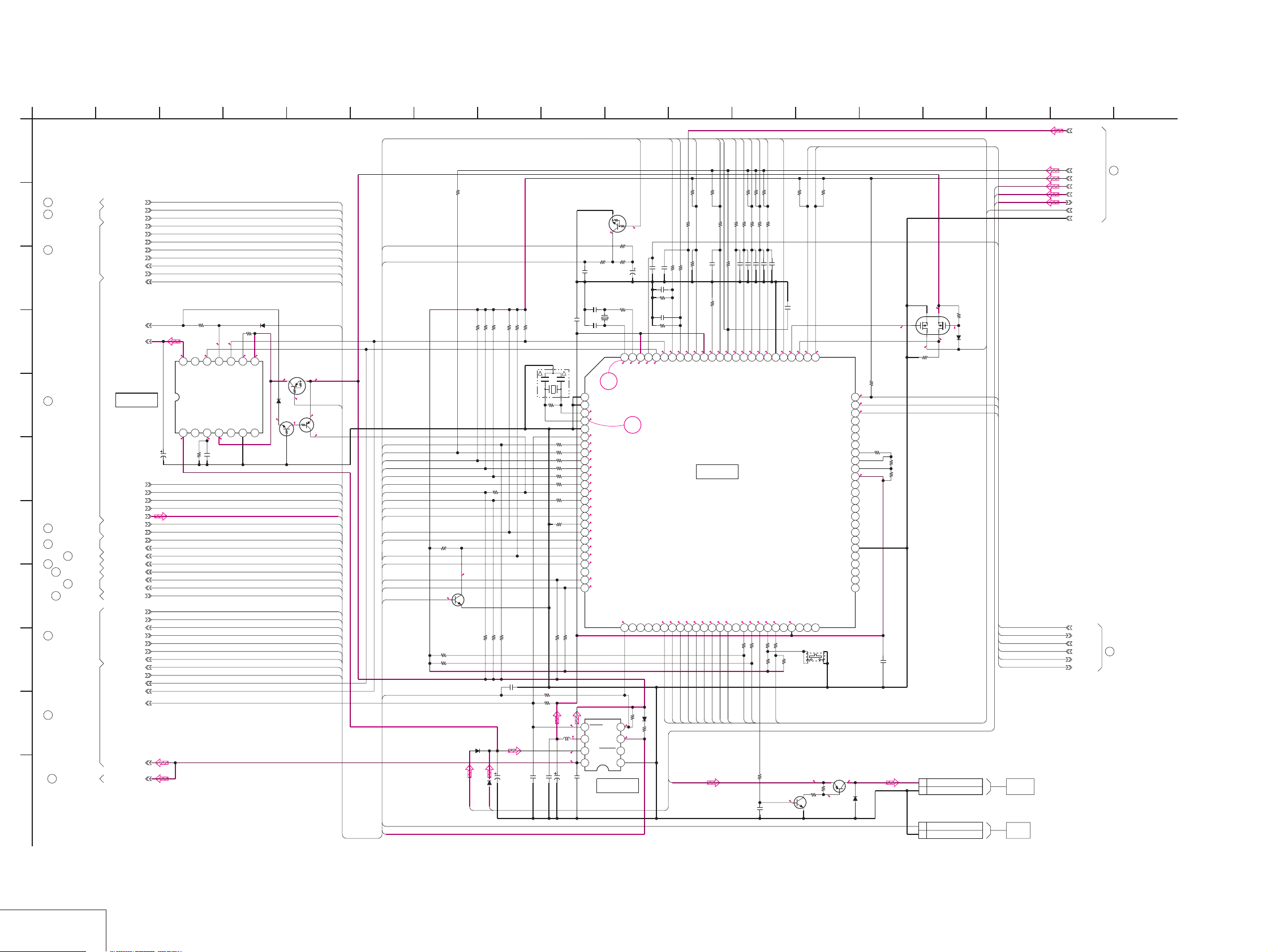
MVC-CD200/CD300
For Schematic Diagram
• Refer to page 4-19 for printed wiring board.
• Refer to page 4-75 for waveforms.
1
SY-67 BOARD(7/10)
HI CONTROL(FR BLOCK)
-REF.NO.:5000 SERIES-
A
XX MARK:NO MOUNT
45
TO(9/10(CN703))
43
B
TO(6/10(CN701))
46
TO(9/10(CN705))
C
D
47
E
TO(9/10(CN709))
F
48
G
H
TO(9/10(CN710))
49
TO(9/10(CN702))
TO(1/10(CN704),
5
3/10,4/10,5/10)
17
13
51
TO(9/10(CN708))
38
TO(5/10)
TO(2/10,4/10)
50
TO(8/10)
TO(1/10,2/10,
4/10)
I
23
TO(3/10(CN707))
J
TO(6/10(CN701),
42
K
9/10(CN709))
16
2
XLENS_CAP_OPEN
XLID_OPEN
TH_OUT
XPB_ON
XPWR_ON
MODE_DIAL
XSETUP_ON
KEY_AD3
LANC_SIG
LANC_DC
IC401
XLANC_JACK_IN
XLID_OPEN
USB_JACK_IN
AV_JACK_IN
XSHTR_ON
XAE_LOCK_SW
XSTB_FULL
STB_CHG
XRST_FLASH
PAL/XNTSC
XRST_SYS
BEEP_ON
BATT/XEXT
INIT_CHARGE
FAST_CHARGE
BATT_SIG
KEY_AD0
KEY_AD1
XPOWER_LED
XCHARGE/STB_LED
KEY_AD2
LANC_OUT
LANC_IN
DIAL_B
DIAL_A
XEJECT
LANC I/O
VL_3V
BEEP
SYS_V
RESET
C401
10u
10V
TA
VDD
VDD
NO MARK:STILL/PB MODE
S :STILL MODE
P :PB MODE
5.5
IC401
TL1596CPWR
1
S7.5
P7.7
R402
470
0.2
12
13NC14
DATA_IN
LANC_DC
UNREG2NC3C.LIM4POWER5NC6GND7NC
0.1
R401
2700
MA111-(K8).S0
R403
XX
3.1
0.2
3.0
9
10
11
WAKE_UP
DATA_OUT
LANC_OUT
3.2
C402
0.1u
B
UN9210J-(K8).SO
D401
8
3.2
VCC
Q401
SWITCH
UN9111J-(K8).SO
MA111-(K8).S0
D402
0.3
Q402
SWITCH
3.2
0
2.8
UN9110J-(K8).SO
XCHARGE/STB_LED
5
XLENS_CAP_OPEN
XLID_OPEN
TH_OUT
XPB_ON
XPWR_ON
MODE_DIAL
XSETUP_ON
KEY_AD3
XLANC_PWR_ON
3.2
XLANC_ON
3.2
3.0
Q403
SWITCH
XLANC_JACK_IN
XLID_OPEN
USB_JACK_IN
AV_JACK_IN
XSHTR_ON
XAE_LOCK_SW
XSTB_FULL
STB_CHG
XRST_FLASH
PAL/XNTSC
XRST_SYS
BEEP_ON
BATT/XEXT
INIT_CHARGE
FAST_CHARGE
BATT_SIG
KEY_AD0
KEY_AD1
XPOWER_LED
KEY_AD2
DIAL_B
DIAL_A
XEJECT
VL_3V
BEEP
SYS_V
MELODY_ENV
BEEP
XPWR_ON
XPB_ON
XLENS_CAP_OPEN
XSHTR_ON
XAE_LOCK_SW
XLID_OPEN
XLANC_PWR_ON
BATT/XEXT
BATT_IN
SYS_V
XSTB_FULL
USB_JACK_IN
AV_JACK_IN
XLANC_ON
XCHARGE/STB_LED
XPOWER_LED
XLANC_JACK_IN
BATT_IN
DEW_SENS
VL_3V
7 15
R419
470k
R425
4700
C410
0.001u
B
C411
22p
CH
C412
C407
18p
0.1u
CH
B
X401
10MHz
12345678910111213141516171819202122232425
GND
GND
1k
1kR467
1kR422
1kR468
1kR469
0R470
1k
1MR423
3.2
3.2
L401
47uH
7.6
3.2
C420
22u
6.3V
A
1.4
10MHz_IN
1.2
10MHz_OUT
GND
3.2
XRESET
3.1
XPWR_ON
S3.0/P0
XPB_ON
3.2
XLENS_CAP_OPEN
3.2
XSHTR_ON
3.2
XAE_LOCK_ON
3.2
XLID_OPEN
3.0
XLANC_PWR_ON
0
BATT/XE
3.2
BATT_IN
3.0
SYS_V
0
DRY_BATT2
3.2
XSTB_FULL
0
USB_JACK_IN
3.3
LANC_JACK_IN
3.2
AV_JACK_IN
0
XLANC_ON
SELF_TIMER_LED_ON(TALLY)
0
XCHARGE/STB_LED
0.4
XPOWER_LED
IC403
NJU7285DV(TE2)
5678
RESET
VOUT VBAT
VIN
VRO VSS
C409
0.1u
B
R421
1M
R466
R478
XX
R475XXR476
470R424
R420
47k
C408
0.1u
B
100k
R404
0
Q404
2SD2216J-QR(K8).SO
SWITCH
10kR407
10k
R408
MA111-(K8).S0
D404
3.3
ACV_UNREG
470k
R418
R474
4700R413
D403
MA111-(K8).S0
470kR410
100k
C404
0.047u
BATT_UNREG
470k
470k
470k
470k
R417
R412
R415
R416
470k
470k
R409
R414
F
C403
C406
10u
4700p
16V
B
B
Q407
UN9213J-(K8).SO
SWITCH
X402
32.768kHz
11
CS
PREEND
IC403
RESET
104 11 136
MELODY
00
R427
2700
R428
10k
C414
C413
XX
3.3u
B
6.3V
TA
C416
0.1u
B
R426
330k
C417
0.1u
B
R432
220k
±0.5%
99
100
1.2
1.6
3.2
3.1
32kHz_IN
MC_HELP
32kHz_OUT
BACK_UP_VCC
10
3.2
UNREG_SCK
CMOD
XCS_DDCON
UNREG_SO
26272829303132
R429
D405
100k
3.2
1SS357-TPH3
R430
150
3.0
N.C
1234
C415
R431
220k
±0.5%
0.2
LANC_OUT
SIRCS_IN
B
R434
0.01u
LANC_IN
3.2
SYS_DD_ON
SYS_DD_ON
ACV_UNREG
BATT_UNREG
R435
± 0.5%
± 0.5%
470k
470k
2.600.2
2.5
ACV_SENS
3.2
0
PAL/XNTSC
PAL/XNTSC
XRST_FLASH
CAM_P_5V
TH_OUT
DEW_SENS
330kR436
1kR471
68kR437
1.8
0
DEW_SENS
BATT_SENS
DD_CON_SENS
MB89098RPFV-G-176-BN
3.2
0
XRST_FLASH
STB_CHG
XRST_SYS
333435
STB_CHG
XRST_SYS
MODE_DIAL
XSETUP_ON
470k
R472
1kR441
R479
1k
B
22kR473
0.047u
C418
1M
R438
0
3.2
3.0
3.103.1
AVCC
T_SENS
MODE_DIAL
XSETUP_ON
DRY_BATT_IN
IC402
HI CONTROL
(FR)
IC402
0
0
0
3.2
INIT_CHARGE
N.C.
INIT_CHARGE
FAST_CHARGE
MELODY_ENV
BEEP_ON
37383940414243444546474849
36
R446
1k
FAST_CHARGE
MELODY_ENV
BEEP_ON
KEY_AD2
KEY_AD3
10kR447
10k
R450
1kR445
1kR448
B
0.047u BC421
0.047u
C419
3.1
KEY_AD2
KEY_AD3
(LCD_CS)
(LCD_COM_XDATA)
0
0
Program_Dial_A
Program_Dial_B
1k
R449
DIAL_B
DIAL_A
C707
XX
B
KEY_AD0
KEY_AD1
10k
R452
1kR453
1k
R451
BC423
BC422
B
0.047u
0.047u
0.047u
C424
0
3.1
GND
KEY_AD1
KEY_AD0
0
3.2
3.2
STRB_PLUNGER_ON
XEJECT
XSTRB_POP_UP
1k
R454
R455
470k
XEJECT
R720
15k
2SD2216J-QR(K8).SO
R456
MELODY
R458
MELODY
SEG16
1k
SWITCH
XX
0.047u
0.2
3.2
R457
470k
Q704
HI_SO
XHI_SCK
C426
B
0.2
3.1
7677787980818283848586878889909192939495969798
HI_SO
BATT_SI
XHI_SCK
BATT_SO
SEG14
SEG15
Vdd
SEG13
50
S401
(FLASH OPEN/CLOSE)
R718
10k
4.9 0
R719
330
R459
XX
2.9
HI_SI
XCS_MC
MC_WAKE_UP
COM3
COM2
COM1
COM0
Vdd
SEG0
SEG1
SEG2
SEG3
SEG4
SEG5
SEG6
SEG7
GND
SEG8
SEG9
SEG10
SEG11
SEG12
Q703
2SA1588-OY-TE85L
STROB PLUNGER DRIVE
4.90
D713
1SS355TE-17
143
2
0.2
6
2.9
R463
100k
R464
100k
3.0
2.9
0
R460
XX
68 69 70 71 72 73 74 75
66 67
51 52 53 54 55 56 57 58 59 60 61 62 63 64 65
R461
XX
R462
3.2
XX
C425
0.1u
B
1
2
1
2
3.2
1
3
VCC
REG_GND
DEW_SENS
REG_GND
HN1L02FU(TE85R)
BATT SIG I/O
4
5
3.0
0.2
D407
MA111-(K8).S0
CN712
CN713
XMC_HELP
Q408
R465
100k
BATT_SIG
XMC_NMI
XMC_CS
1612
CAM_P_5V
BATT_UNREG
ACV_UNREG
SYS_DD_ON
HI_SI
XMC_HELP
XMC_CS
XMC_NMI
HI_SI
HI_SO
XHI_SCK
PL901
2P
STROB
PLUNGER
2P
DEW
SENSOR
1789
D_1.8V
CAM_3.1V
D_3.4V
CAM_P_5V
BATT_UNREG
ACV_UNREG
SYS_DD_ON
REG_GND
XMC_HELP
XMC_CS
XMC_NMI
HI_SI
HI_SO
XHI_SCK
18
52
TO(10/10)
33
TO(4/10)
HI CONTROL
SY-67 (7/10)
4-35 4-36
Page 21
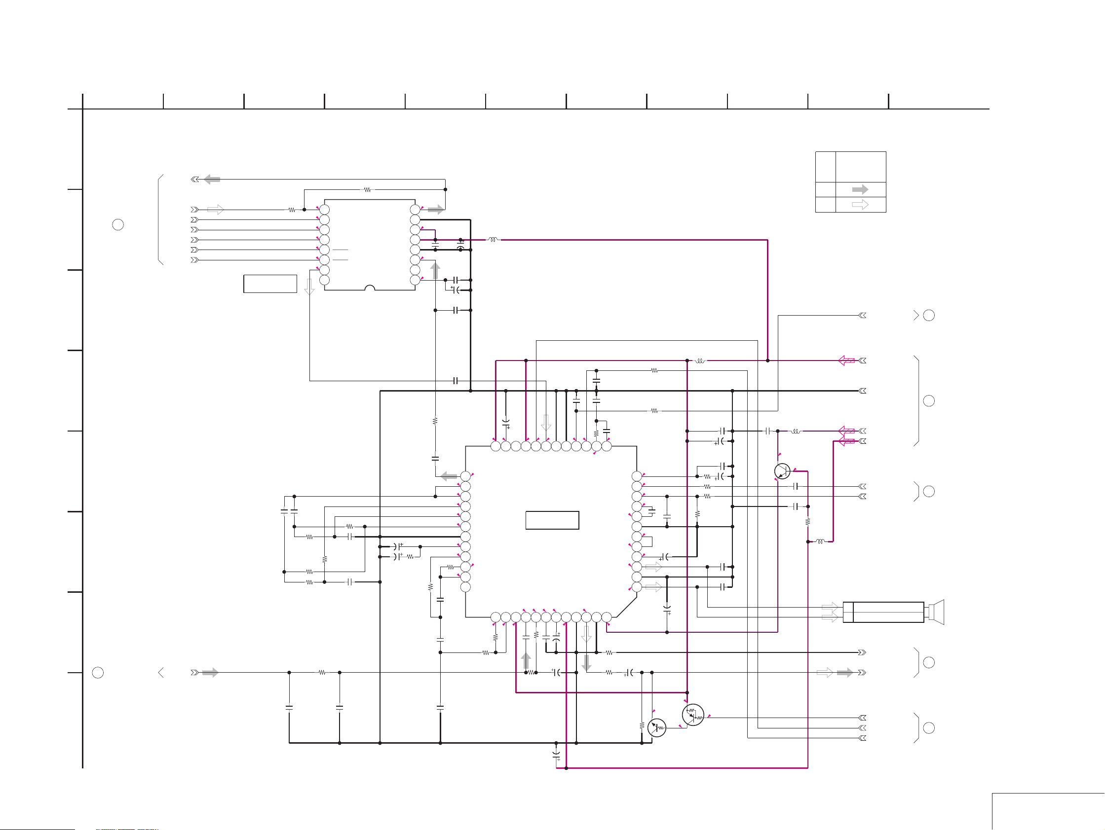
For Schematic Diagram
• Refer to page 4-19 for printed wiring board.
1
2589
MVC-CD200/CD300
3
7
104 116
SY-67 BOARD(8/10)
AUDIO PROCESS(AU BLOCK)
-REF.NO.:5000 SERIES-
A
XX MARK:NO MOUNT
19
TO(2/10)
B
C
D
E
F
G
53
TO(9/10(CN711))
H
16
AU_SDTO
AU_SDTI
AU_LRCK
AU_MCLK
AU_SCLK
AU_XPWAD
AU_XPWDA
MIC_SIG
NO MARK:STILL/PB MODE
S :STILL MODE
P :PB MODE
R265
0
0
0
0
0
0
0
0
IC251
AUDIO AD/DA
C253
0.01u
B
C251
XX
C254
0.022u
R257
B
R253
2200
1500
R252
1500
B
R251
1200
9
10
11
12
13
14
15
16
PWAD
PWDA
R254
SDTI
LRCK
MCLK
SCLK
AOUTL
AOUTR
R256
0
R263
AK4550VT-E2
2200
C255
6800p
B
C256
2200p
B
C252
XX
B
IC251
SIGNAL PATH
AUDIO
B
B
10
L251
REC
PB
SIGNAL
1
SP+
2
SP-
SP_VOL
A_3.4V
REG_GND
CAM_P_5V
A_4.9V
BEEP
BEEP_ON
CN706
AU_GND
AU_OUT
XAU_LINE_MUTE
AU_HGL_SEL
XAU_SP_MUTE
2P
8
TO(1/10)
54
TO(10/10)
50
TO(7/10)
55
TO(9/10(CN709))
34
TO(4/10)
SP901
SPEAKER
XX
R260
C260
0.47u
1u 16V
R261
47k
R262
0
8
7
3.3
C265
6
1u
B
5
4
0
3
2
1
470
B
27k
C272
0.01u
B
0
C267
10u
6.3V
C268
2200p
B
C269
0.47u
B
1.6
1.6
1.6
1.6
1.6
0
1.6
47k
R259
1.6
C261
0.015u
C262
0.015u
C257
0.01u
B
C270
10u
6.3V
0
REC_OUT
25
BIAS
26
LPF_OUT
27
LPF_IN2
28
LPF_IN1
29
AGC_OUT
30
GND
31
AGC_DET
32
WHPF_OUT
33
1.6
WHPF_BIAS
34
WHPF_IN
35
LING_IN
36
R266
R264
2200
L252
10uH
C264
6.3V
10u
3.3
1.6
23
24
STBY
VREF
22
21
MIC_OFF
3.301.6
20
VCC
LPF_SEL
19
18
PB_IN
SPAGC_ON/OFF
IC252
AUDIO AMP
IC252
AN2905FHQ-EB
1.6
2.0
1.2
B
0.1u
R268
2.4
100
R267
C275
C274
10u
1u
6.3V
B
C273
1k
10u
10V
C276
10V
10u
MIC_OUT39WIND_ON40MIC_IN412VOUT42VREG_C43VREF_H44VCCH45GND46LINE_OUT47SP_SAVE48SP_VCC
GAIN_SET
37
38
1.7
1.7
33k
3.3
C266
17
4.9
C277
1u
AGND
F
S1.2/P2.2
0.5
15
16
VOL_CTL
2.4
C278
0.1u
B
C283
0.1u
B
C280
100
R273
2.2
13
14
2.4
MIX_IN
VOL_OUT
SPAGC_DET
BEEP_IN
XAUDIO_MUTE
XBEEP_MUTE
BEEP_OUT
BEEP_MIX_IN
MIX_OUT
SPA_IN
VREF_SP
SP_OUT-
SP_GND
SP_OUT+
4.4
R270
0
R272
2200
0.47u
AGND
10uHL253
R274
33k
R271
2200
B
0
12
2.4
11
0.4
10
2.4
9
10u
R276
100k
8
7
6
5
4
3
2
1
0.47u
2.2
2.2
C282
10V
C281
10u
B
C285
10u
6.3V
3.3
0
3.3
UN9216J-(K8).SO
C284
0.047u
Q251
MUTE
B
2.2
2.2
2.2
2.2
C279
6.3V
C286
1u
C291
1u
R278
47k
68k
R280
R279
100k
R277
47k
C289
0.01u
C290
0.01u
Q252
UN9113J-(K8).SO
SWITCH
0
C293
L254
10uH
1u
B
4.4
4.9
Q253
FMMT617TA
SP VOL SW
4.9
C292
0.47u
C294
0.01u
R281
10uH
F
C287
10u
6.3V
B
C288
4.7u
6.3V
B
B
C259
SDTO
DEM1
DEM0
AINL
AINR
VCOM
C258
4.7u
6.3V
VDD
VSS
4-37 4-38
AUDIO PROCESS
SY-67 (8/10)
Page 22
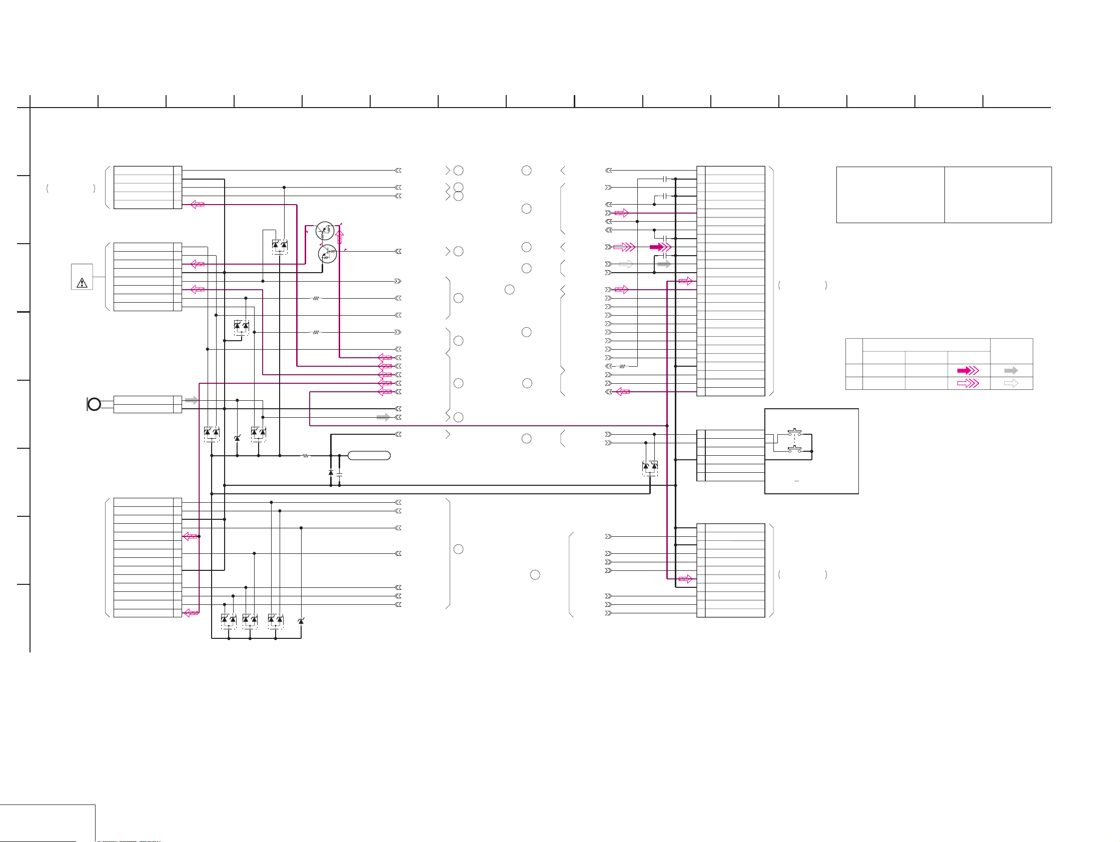
MVC-CD200/CD300
For Schematic Diagram
• Refer to page 4-19 for printed wiring board.
1
2589
7 15
104 11 136
12
143
SY-67 BOARD(9/10)
CONNECTOR(CN BLOCK)
-REF.NO.:5000 SERIES-
A
XX MARK:NO MOUNT
TO
TK-61 BOARD
CN501
THROUGH THE
FP-369 FLEXIBLE
(SEE PAGE
4-18)
B
FLASH
UNIT
C
FLASH UNIT is replaced as a block.
So the PRINTED WIRING BOARD and
SCHEMATIC DIAGRAM are omitted.
D
MIC901
E
F
TO
CONTROL SWITCH
G
BLOCK(ZK-503)
(SEE PAGE
4-55)
H
16
CN703
CN702
5P
SELF_TIMER
REG_GND
LENS_CAP_OPEN
PRELAMP_AF_ON
CAM_P_5V
8P
STB_CHARGE
STRB_PHOTO_ON
A_4.9V
UNREG_GND
PHOTO_TR_OUT
UNREG
STROB_ON
XSTB_FULL
2PCN711
MIC_SIG
MIC_GND
14PCN705
DIAL_B
DIAL_A
KEY_AD3
CAM_3.1V
XPOWER_ON
XPB_ON
XSET_UP
MODE_DIAL
CAM_3.1V
NO MARK:STILL/PB MODE
5
4
3
2
1
1
2
3
4
5
6
7
8
1
2
D701
XX
1
2
3
GND
4
5
6
N.C
7
8
N.C
9
GND
10
N.C
11
12
13
14
D707
XX
D708
D702
XX
D714
XX
Note: Resistor is mounted to the location
where FB701 is printed.
UN9113J-(K8).SO
R723
R724
FB701
0
Note
D704
1SS352-TPH3
D710
XX
SWITCH
S4.9/P0
0
1k
MAZS082008SO
D705
D703
XX
XX
D709
XX
Q701
S0/P4.8
4.9
S3.1/P0
Q702
UN9213J-(K8).SO
SWITCH
LND701
FLAME_GND
C701
2200p
B
SELF_TIMER
XLENS_CAP_OPEN
PRELAMP_AF_ON
CAM_DD_ON
STRB_AIN
STRB_ON
STRB_PHOTO_ON
XSTB_FULL
STB_CHG
A_4.9V
CAM_P_5V
ST_UNREG
CAM_3.1V
D_3.4V
REG_GND
MIC_SIG
LND702
DIAL_B
DIAL_A
KEY_AD3
XPWR_ON
XPB_ON
XSETUP_ON
MODE_DIAL
36
45
7
35
22
49
57
53
NOT USE
46
TO(4/10)
TO(7/10)
TO(1/10)
TO(4/10)
TO(2/10)
TO(7/10)
TO(10/10)
TO(8/10)
TO(7/10)
TO(6/10(CN701),
42
7/10)
CN709
21
TO(2/10)
47
TO(7/10)
28
TO(3/10)
55
TO(8/10)
29
TO(4/10)
47
TO(7/10)
EXT_STRB_ON
LANC_SIG
XLANC_JACK_IN
LANC_DC
USB_JACK_IN
AV_JACK_IN
AU_OUT
AU_GND
USB_D+PULLUP
USB_D+OUT
USB_D-OUT
USB_TXENL
USB_XVDATA
USB_D+IN
USB_D-IN
USB_SUSPND
USB_VBUS
XEJECT
XLID_OPEN
V_OUT
VL_3V
C703
0.1u
B
C704
0.1u
B
C705
0.1u
B
C706
2200p
B
VDD
R711
0
27
26
25
24
23
22
21
20
19
18
17
16
15
14
13
12
11
10
9
8
7
6
5
4
3
2
1
EXT_STROB_ON
REG_GND
LANC_SIG
REG_GND
XLANC_JACK_IN
LANC_DC
USB_DET
AV_JACK_IN
REG_GND
V_OUT
REG_GND
A_OUT
REG_GND
D_3.4V
VDD
USB_D+PULLUP
USB_D+OUT
USB_D-OUT
USB_TXENL
USB_XVDATA
USB_D+IN
USB_D-IN
USB_SUSPND
REG_GND
XEJECT
XLID_OPEN
VL_3V
27P
TO
JK-208 BOARD
CN101
THROUGH THE
FP-361 FLEXIBLE
(SEE PAGE 4-57)
Note :
The components identified by
mark 0 or dotted line with mark
0 are critical for safety.
Replace only with part number
specified.
SIGNAL PATH
VIDEO SIGNAL
REC
PB
Note :
Les composants identifiés par
une marque 0 sont critiques
pour la sécurité.
Ne les remplacer que par une
pièce portant le numéro spécifié.
Y/CHROMAY SIGNALCHROMA
AUDIO
CONTROL SWITCH
BLOCK(RL-503)
6P
XSHTR_ON
XAE_LOCK_SW
NC
GND
NC
NC
REG_GND
BATT_SIG
REG_GND
BATT/XEXT
FAST_CHARGE
INIT_CHARGE
D_3.4V
REG_GND
POWER_LED
KEY_AD0
KEY_AD1
CN710
CN708
(SHUTTER)
LOCK
ON
CONTROL SWITCH BLOCK(RL-503) is replaced as a block.
So the PRINTED WIRING BOARD is omitted.
11P
TO
FS-83 BOARD
CN001
THROUGH THE
FP-362 FLEXIBLE
(SEE PAGE 4-57)
48
TO(7/10)
51
TO(7/10)
XSHTR_ON
XAE_LOCK_SW
BATT_SIG
BATT/XEXT
FAST_CHARGE
INIT_CHARGE
XPOWER_LED
KEY_AD0
KEY_AD1
D712
XX
1
2
3
4
5
6
11
10
9
8
7
6
5
4
3
2
1
CONNECTOR
SY-67 (9/10)
4-39 4-40
Page 23
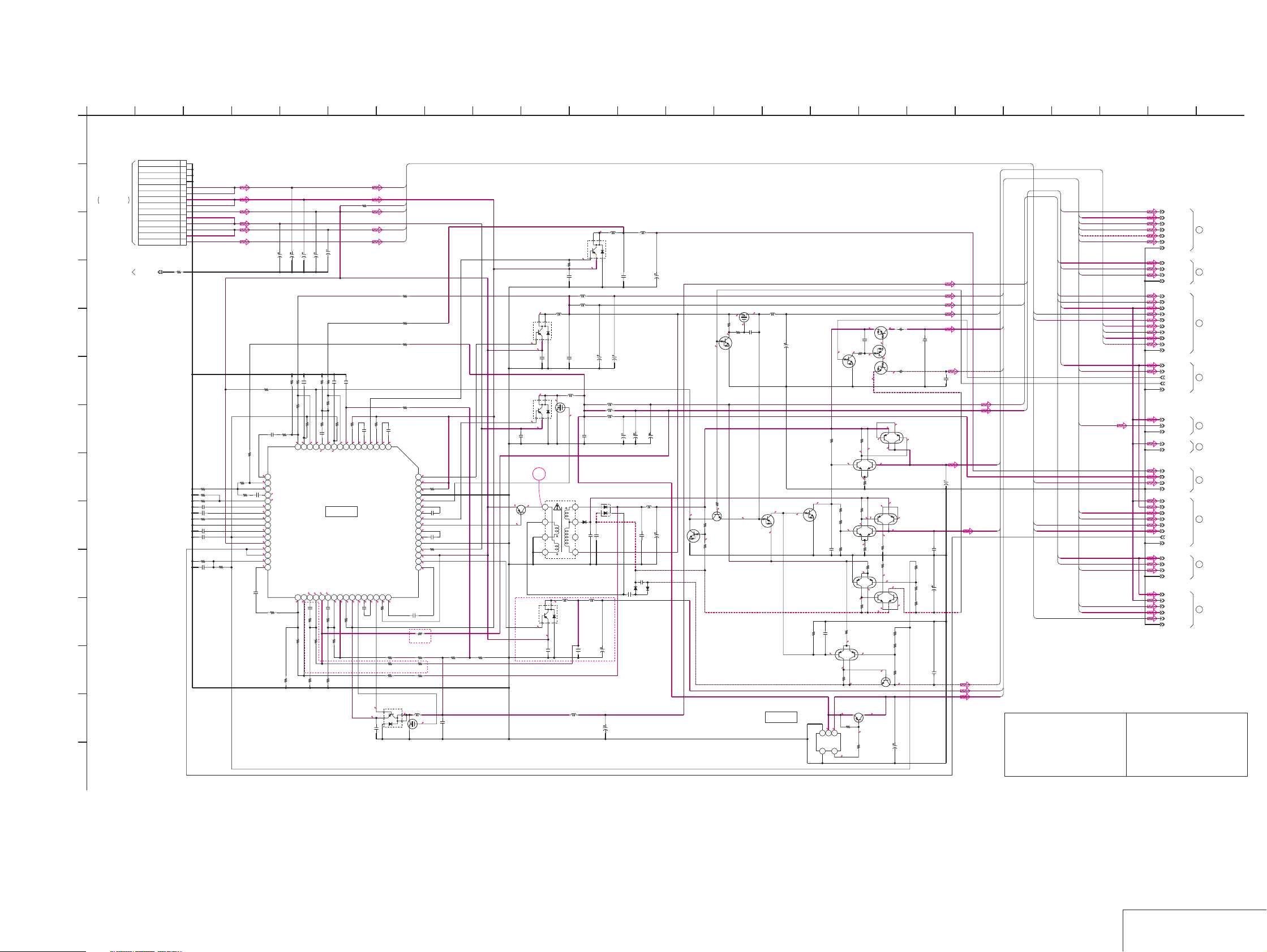
For Schematic Diagram
• Refer to page 4-19 for printed wiring board.
• Refer to page 4-75 for waveform.
1
SY-67 BOARD(10/10)
DC/DC CONVERTER(DD BLOCK)
A
-REF.NO.:5000 SERIES-
B
XX MARK:NO MOUNT
TO
FS-83 BOARD
CN004
TUROUGH THE
FS-136 HARNESS
(SEE PAGE
4-58)
CN001
C
NOT USE
D
E
F
G
H
I
J
K
L
M
N
16
LND702
2
14P
D_4.6V/1.8V
D_4.6V/1.8V
HI_UNREG
D_3.4V/3.2V
D_3.4V/3.2V
ST_UNREG
ST_UNREG
BATT_UNREG
REG_GND
REG_GND
REG_GND
REG_GND
P_4.6V
P_4.6V
3 23
NO MARK:STILL/PB MODE
S :STILL MODE
P :PB MODE
14
13
12
11
10
9
8
7
6
5
4
3
2
1
R006
XX
1608
R010
8200
±0.5%
R007
33k
±0.5%
R011
XX
33k
R009
33k
C007
0.01u
± 0.5%
0.068u
0.033u
R001
33k
±0.5%
R002
R003
24k
C001
180p
CH
C002
B
R004
C003
B
C004
0.1u
B
R005
150k
C005
1u
B
MVC-CD200/CD300
5
C016
C017
C019
10u
10u
10u
16V
16V
16V
TA
TA
TA
R016
15k
±0.5%
C009
R014
XX
R024
27k
R008
±0.5%
47k
±0.5%
C008
0.001u
B
S1.1/P0.8
FB5
17
3.0
18
IN(C)4
1.5
-IN(E)4
19
8200
0.9
FB4
20
0.8
2200pBC006
RT
21
1.2
RC
22
0
CSCP
23
0
MOS DUTY
24
GND2
25
2.0
26
CS(SOFT START)1,2,4
1.5
VREF
27
8.4
VCC
28
3.2
CTL2
29
3.2
CTL1
30
1.2
DTC3
31
0.8
FB3
32
B
R012
6800
R015
4700
± 0.5%
27k
±0.5%
R017
47k
0
R013
33k
R019
1.5
4.1
1.5
13
14
15
16
IN(C)5
-IN(E)5
+IN(E)5
S1.1/P0.7
1.5
-IN(E)334IN(C)335FB236-IN(E)237IN(C)238FB139-IN(E)140IN(C)141VB142VCC1,343OUT2-144CB1-145CB2-146OUT1-147VB248CB1-2
33
B
1.5
2.5
0.01u
3900
R020
C010
R018
±0.5%R022 47k
3300
±0.5%
R021
*
R021
0 :MVC-CD200
27k:MVC-CD300
6 20
R076
0
C021
C022
10u
10u
16V
16V
TA
TA
R027
10k
±0.5%
C013
C063
XX
XX
B
±0.5%
R028
22k
R025
8.4
12
0.7
FB6
SCP
4.1
47k
B
0
0.001u
R033
1.5
4.1
C011
8
9
10
11
1.5
IN(C)6
-IN(E)6
OVP5,6
+IN(E)6
IC001
DC/DC CONVERTER
IC001
MB3825APFV-G-BND-ER
0.8
B
1.5
1.6
0.022u
470R029
C012
R037
22k
R031
3300
±0.5%
MVC-CD300
R030
33k
±0.5%
C014
0.001u
B
R038
10k
1.8
8.3
S8.9
5
7
VB6
3.4
7.7
8.2
C015
0.001u
7 15 22
CW_UNREG
ACV_UNREG
BL_UNREG
ST_UNREG
BATT_UNREG
R036
0
R034
0
R035
0
R085
0
R039
10k
C018
0.001u
B
8.3
S8.9/P7.8
S7.6/P7.9
S6.8
P7.4
S8.3
P8.8
P9.0
1
3
4
VB5
CB2-52CB1-5
CB2-66CB1-6
OUT1-6
S8.0/P8.3
OUT1-5
64
8.4
VCC4,5,6
63
R041
10k
VB4
62
S7.9/P8.2
61
GND4,5,6
2.6
OUT2-4
60
8.5
CB1-4
59
C023
7.1
C020
0.001u
B
R083
R045
R043
R044
L006
22uH
SI2304DS-T1
0
0
0
SWITCH
0.001u
58
B
8.1
57
8.2
56
S7.0/P7.6
C024
55
0.001u
B
54
S8.5/P8.9
53
R042
22k
52
S7.6/P8.1
51
2.2
50
S7.7
P7.9
49
S6.6
P8.1
MVC-CD200
R046
R047
100k
0
0
C034
3.4
4.7u
6.3V
B
Q008
2012
CB2-4
OUT1-4
OUT1-3
CB2-3
CB1-3
GND1,2,3
VB3
VCC2
OUT1-2
CB2-2
8.1
8.6
R040
22k
S7.4/P8.4
S7.1/P7.4
S8.0/P8.3
B
R032
3300
±0.5%
15k
R023
±0.5%
R026
39k
±0.5%
Q006
FP107-TL
D 1.8V REG
8.1
8.2
C028
4.7u
10V
B
3216
1.8
Q001
FP107-TL
4.9V REG
S7.9/P8.2
Q005
FP107-TL
3.4V REG
Q002
2SB1122-ST-TD
SWITCHING
8.2
8.2
FP107-TL
CAM 5V REG
S8.2/P8.4
C026
4.7u
B
Q003
C027
4.7u
B 3216
7.9
8.2
10V
3216
0
CW D 4.6V REG
L001
47uH
5.0
C030
4.7u
10V
10V
B
L004
3.4
22uH
3.4
1
T001
DC/DC CONVERTER
TRANSFORMER
1234
4.9
7.9
8.4
C029
4.7u
10V
B
3216
SI2304DS-T1
FP107-TL
S8.1/P8.3
Q007
SWITCH
L007
47u
±20%
Q004
R084
4.7u
2.6
L009
4.7uH
33k
C025
10V
3216
B
1SS357-TPH3
S4.7/P0
S8.2
P8.4
L005
4.7uH
L002
4.7uH
C032
10u
10V
TA
L014
4.7uH
L011
4.7uH
C033
4.7u
10V
B 3216
D001
D002
MA796-TX
41
5678
32
C035
C038
4.7u
4.7u
3216
3216
F
F
L010
4.7u
±10%
C044
C036
4.7u
10V
10V
B
MVC-CD300
L008
1uH
L003
47uH
C041
C031
4.7u
C037
10u
10V
TA
4.7uH
L016
C062
C046
10u
10u
10V
10V
TA
C039
0.1u
2012
10u
TA
C042
10u
6.3V
TA
10u
10V
TA
10V
B
3216
C049
10u
10V
TA
TA
L013
220uH
C045
4.7u
F
3216
C043
0.1u
2012
F
F
D004
1SS355TE-17
D003
1SS355TE-17
8.4
C048
4.7u
25V
TA
B
3.1
R052
100k
R050
47k
1.7
R051
22k
1005
UN9213J-(K8).SO
Q011
PANEL 4.9V SW
R048
100k
0
Q012
2SD2216J-QR(K8).SO
3.1
Q010
SWITCH
4.9
SWITCH
14
NDS356AP
0
R049
100k
Q009
SWITCH
UN9213J-(K8).SO
4.9
UN9113J-(K8).SO
SWITCH
1612
L015
4.7uH
4.9
C050
0.022u
B
C051
10u
10V
TA
UN9213J-(K8).SO
Q014
UN9213J-(K8).SO
SWITCH
0
3.3
IC002
CAM 3.1V REG
0
HN1A01FE-Y/GR(TPLR3)
HN1A01FE-Y/GR(TPLR3)
PANEL -15.3V REG
Q013
Q023
SWITCH
12.8
C053
0.47u
2012
Q016
CAM -7.5V REG
R053
15k
Q015
IC002
XC62EP3102MR
B
123
3.3
S3.1
P0
PANEL 13.2V REG
R054
33k
±0.5%
R057
120k
±0.5%
R058
6.4
R059
±0.5%
C052
0.47u
B
2012
1
0
2
6
S-34.7
P-34.5 S-34.6
R055
100k
3.3
3.1
R080
45
S2.4
P2.6
178 219
Note: Ferrites are mounted to the location
where R075, R077 are printed.
14.614.7
S2.8
P14.6
10k
S0.4/P14.5
7.5
14.2
14.7
3
1
4
R065
100k
HN1C01FE-Y/GR(TPLR3)
PANEL 6.5V REG
S8.5
P8.4
S8.9
P8.8
S9.0/P8.9
2
6
3
1
4
R064
47k
R062
82k
4
6
-9.8
3
2
-9.2
-9.8
HN1C01FE-Y/GR(TPLR3)
0
Q017
P-34.5
3.1
2.7
R079
1k
UN9113J-(K8).SO
CAM 15V SW
Q024
UN9113J-(K8).SO
SWITCH
S2.8/P-7.5
UN9213J-(K8).SO
CAM -7.5V SW
S-7.5
14.7
1
2
6
13.0
13.012.8
5
Q019
HN1C01FE-Y/GR(TPLR3)
PANEL 13.2V REG
Q018
S9.0/P8.9
1
4
3
6
5
0
R070
4700
R069
10k
S-0.1
0
5
3
6
1
4
Q020
CAM -7.5V REG
R067
1800
± 0.5%
C061
10u
10V
TA
Q025
Q026
R077
P0
0uH
Note
14.2
4
3
5
6.5
P0
-7.5
5
R066
10k
± 0.5%
R068
120k
± 0.5%
-15.7
C058
1u
F
2012
S0
P14.5
R074
Q021
HN1A01FE-Y/GR(TPLR3)
R063
100k
14.5
6
2
12.4
R061
47k
S8.9
P8.8
0
2
S8.4
120k
P6.0
0.5
1
2
-8.7
R060
100k
R056
100k
0.4
4
5
3
2SD2216J-QR(K8).SO
PANEL-15.3V SW
S-35.2
P-35.00
Q027
CPH3106-PM-TL
CAM 3.1V REG
47k
R075
0uH Note
5
14.5
Q022
HN1A01FE-Y/GR(TPLR3)
PANEL 6.5V REG
S8.5
P8.4
0V
-9.2
18
C064
XX
C065
XX
C056
2.2u
F
2012
R071
18k
±0.5%
C057
R072
10u
22k
16V
±0.5%
TA
B
R073
68k
±0.5%
C054
1u
B
3216
19
D_3.4V
CAM_15V
CAM_5V
CAM_3.1V
CAM_-7.5V
CAM_P_5V
A_3.4V
D_1.8V
D_1.8V
CAM_P_5V
A_4.9V
PANEL_4.9V
CAM_15V
CAM_-7.5V
PANEL_13.2V
C055
1u
25V
A
TA
PANEL_6.5V
PANEL_-15.3V
CAM_5V
CAM_3.1V
ACV_UNREG
BL_UNREG
A_3.4V
D_3.4V
CW_UNREG
ACV_UNREG
BATT_UNREG
ST_UNREG
CAM_3.1V
A_4.9V
A_3.4V
D_3.4V
PANEL_4.9V
PANEL_13.2V
PANEL_6.5V
PANEL_-15.3V
D_1.8V
CAM_3.1V
CAM_3.1V
CAM_3.1V
CAM_P_5V
A_4.9V
A_3.4V
CAM_P_5V
CAM_3.1V
CAM_P_5V
Note :
The components identified by
mark 0 or dotted line with mark
0 are critical for safety.
Replace only with part number
specified.
D_3.4V
CAM_15V
CAM_5V
CAM_3.1V
CAM_-7.5V
CAM_P_5V
REG_GND
A_3.4V
D_1.8V
CAM_3.1V
REG_GND
A_4.9V
A_3.4V
D_3.4V
ACV_UNREG
BL_UNREG
PANEL_4.9V
PANEL_13.2V
PANEL_6.5V
PANEL_-15.3V
REG_GND
D_1.8V
CAM_3.1V
CAM_DD_ON
LCD_DD_ON
REG_GND
D_3.4V
CAM_3.1V
REG_GND
D_3.4V
REG_GND
CW_D_4.6V
CW_D_3.4V
CW_UNREG
REG_GND
D_3.4V
D_1.8V
CAM_3.1V
CAM_P_5V
ACV_UNREG
BATT_UNREG
SYS_DD_ON
REG_GND
A_4.9V
A_3.4V
CAM_P_5V
REG_GND
A_4.9V
D_3.4V
CAM_3.1V
CAM_P_5V
ST_UNREG
REG_GND
Note :
Les composants identifiés par
une marque 0 sont critiques
pour la sécurité.
Ne les remplacer que par une
pièce portant le numéro spécifié.
3
14
25
30
37
40
44
52
54
57
24104 11 13
TO(1/10)
TO(2/10)
TO(3/10)
TO(4/10)
TO(5/10)
TO(6/10)
TO(6/10(CN701))
TO(7/10)
TO(8/10)
TO(9/10)
4-41 4-42
DC/DC CONVERTER
SY-67 (10/10)
Page 24
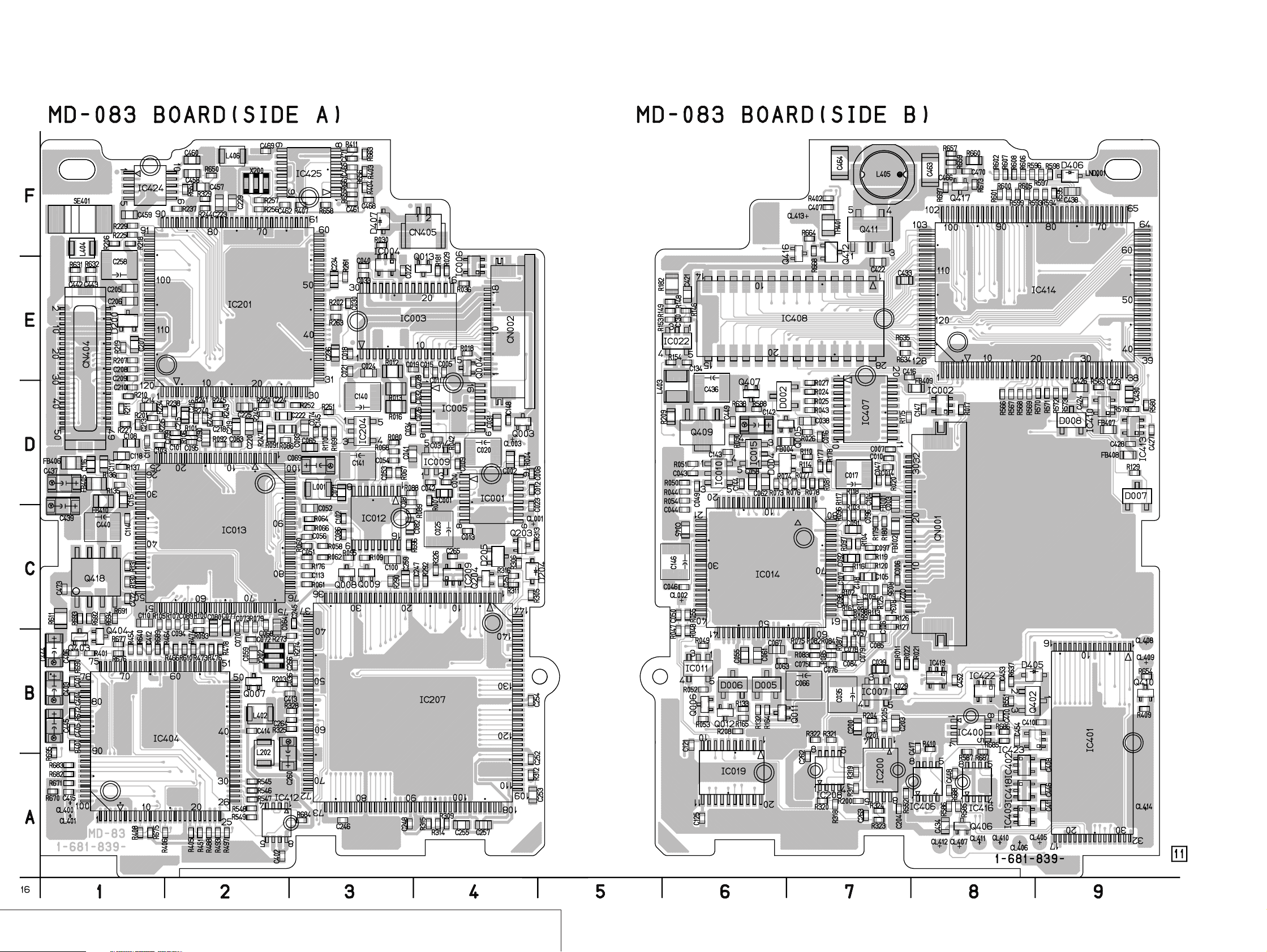
MVC-CD200/CD300
MD-083 (CD-RF PROCESS, SERVO, CD, DSP, CD-R/RW GA, MD SYSTEM CONTROL, EFM/ENC CONTROL)
PRINTED WIRING BO ARD
— Ref. No. MD-083 Board; 3,000 Series —
• Refer to page 4-45 for note and circuit boards location.
CD-RF PROCESS, SERVO, CD, DSP, CD-R/RW GA, MD SYSTEM CONTROL, EFM/ENC CONTROL
MD-083
4-44
Page 25
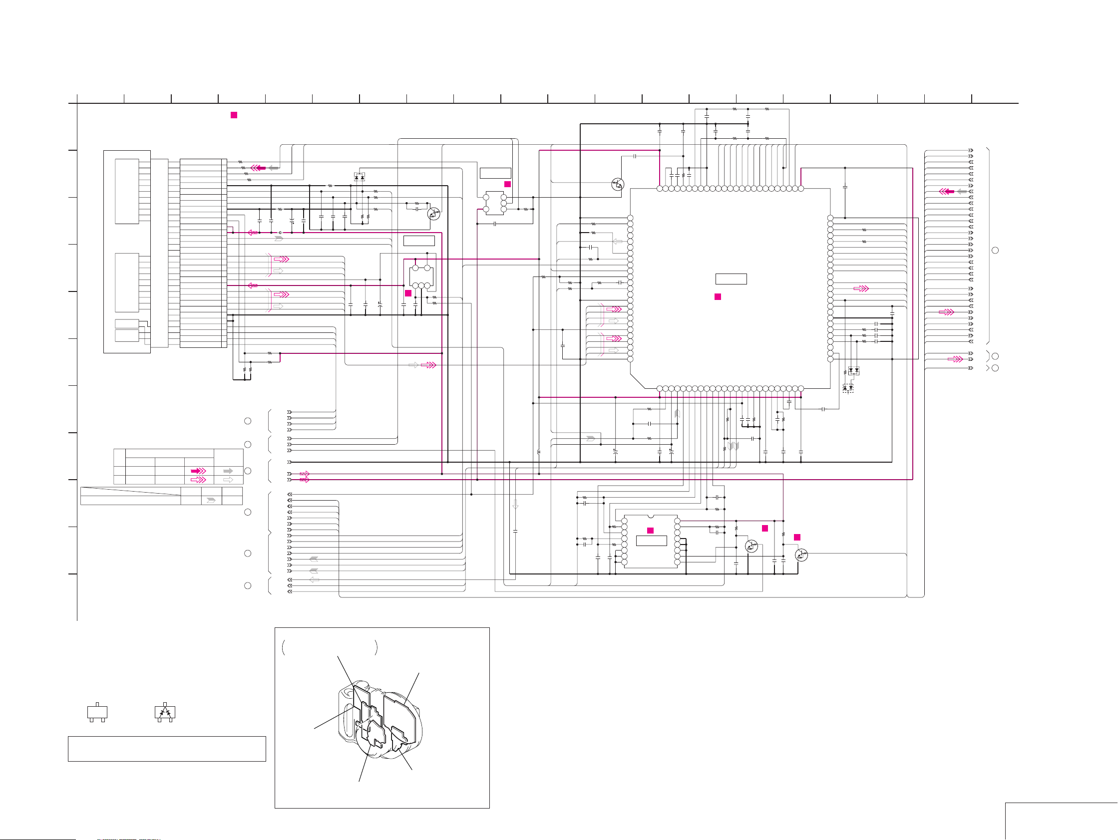
For Schematic Diagram
• Refer to page 4-43 for printed wiring board.
OPTICAL
DEVICE
FOCUS
COIL
TRACKING
COIL
2
Measurement at Mark is not possible
physically due to the parts mounted on
Side B.
When disk access fails,supply of power is
stopped due to power save.As the result,
most of the measurement points show"0"(zero).
32PCN001
OSCON
LDGND
VWDC1
VWDC2
VRDC
PGND
CMOD
CFREQ
FLEXIBLE
FP-372
PD
LDD5V
LDD5V
FPDVC
FPDO
NC
E
C
D
G
VC
VCC
H
A
B
F
GND
FGND
FCS+
1
MD-083 BOARD(1/5)
CD-RF PROCESS(ANALOG BLOCK)
-REF.NO.:3000 SERIES-
A
XX MARK:NO MOUNT
BASE UNIT(1/2)
B
C
D
E
F
G
SIGNAL PATH
H
REC
PB
Ref.signal
I
CHROMA
VIDEO SIGNAL
Y
Y/CHROMA
REC PBREC/PB
J
K
32ENBL
31W/XR
30ODON
29
28
27
26
25
24
23
22
21
20
19
18
17
16
15
14
13
12
11
10
9
8
7
6
5
4
3TRK+
2TRK-
1FCS-
AUDIO
SIGNAL
MVC-CD200/CD300
5
Note: Resistors are mounted to the location
where FB001, FB004 are printed.
EQEFM
ODPLS
FB001
FB002
0uH
EJECT
4.6V_2
RECD2
VREF+
SWDT
XSDLTRF
LDLMT
VWDC2
HAVCOS
OSCON
D002
1S2837-T1
FB004
0
Note
Note
0
C017
C047
C010
0.1u
22u
3300p
C014
B
10V
TA
FCS+
FCS-
TRK+
TRK-
LDEN
GND
4.6V
VC
XTOK
SDCK
DIAG
FE
TEO
TE
RFAC
RRF
MPP
C016
B
0.01u
0.01u
B
B
PD-E
PD-C
PD-D
PD-G
PD-H
PD-A
PD-B
PD-F
FCS+
TRK+
TRK-
FCS-
FCS+
FCS-
TRK+
TRK-
RECD2
XTOK
VREF+
SWDT
SDCK
XSDLTRF
R175
0
0
R021
0
R022
100
R011
C003
C007
0.22u
0.1u
B
B
1608
R179
XX
R180
R177
R178
10k
XX
10k
1
TO(2/5)
2
TO(4/5)
WAPCFUP
6
TO(5/5)
3
TO(2/5)
4
TO(2/5)
5
TO(3/5)
7 15
XRW
LDLMT
R024
VWDC
0
220
R043
VRDC
R020
4700
R027
R025
XX
XX
FPDIN
VREF+
C035
C006
C027
0.1u
0.1u
B
B
C038
XX
B
1608
IC007
OFFSET AMP
IC007
123
TA75S01F(TE85R)
C029
0.1u
B
22u
C039
10V
0.47u
TA
B
EJECT
LDEN
VWDC2
XXR026
Q005
XX
45
3300R034
HAVCOS
R035
470
DIAG
LDLMT
VWDC2
HAVCOS
TEO
RRF
MPP
IC002
AND GATE
TC7SET08FU(TE85R)
45
DIAG
FE
TE
104 11 136 20
C072
C064
0.22u
0.047u
B
B
1608
LDEN
EJECT
IC002
R017
47k
123
C147
0.1u
B
EQRF
C113
0.01u
B
XDFCT2
RRF
EQRF
TEO
MPXO
R058
22k
RRF
VREF+
FPDIN
VREF+
L001
1uH
R061
0
R176
10k
3300p
R062
4700
R060
22k
R066
R064
2200
XX
PD-A
PD-B
PD-C
PD-D
PD-E
PD-F
C052
PD-G
0.22u
B
PD-H
1M
R067
C053
0.022u
B
R068
XX
C054
0.1u
B
C071
0.47u
B
VWDC
C059
1608
Q007
XX
C051
B
C056
10p
CH
C141
22u
10V
TA
IC012
1
Y1
4700
R086
2
Y0
3
Z1
4
Z
R080
4700
5
Z0
6
INH
7
VEE
C074
8
VSS
XX
C068
C070
6800p
XX
B
76
AVSSI
77
RRFTOP
78
RRFBTM
79
N.C.
80
EQRF
81
N.C.
82
AUX1
83
AUX2
84
AUX3
85
MPXOUT
86
RRFVC
87
RECDIN
88
RRF
89
WRF
90
VSS
91
AIN
92
BIN
93
CIN
94
DIN
95
HAVC
96
EIN
97
FIN
98
GIN
99
HIN
100
AVSS3
R169
XX
IC012
4700p
B
B
72
73
74
75
PBHO
PHD2C
AVDD1
RCCMPI
AVDD32FPDIN3FVREF4FPDO5WREF6VWDC7VWDCN8RREF9VRDCN10VRDC11MPP12TEIN13TE14FE15VREF16AGND117BIAS18VSS19LOOP320LOOP221LOOP122BUF023LPF124LPF025AVDD2
1
C145
XX
CH
R170
0
C065
C069
0.22u
10u
B
TA
1608
BU4053BCFV-E2
VDD
Y
X
X1
X0
SWITCH
A
B
C
143
62
DFCT
SLHOLD
R105
C089
10k
0.01u
B
C094
R107
0.01u
10k
B
RAPC
SSMP
ASMP
RSMP
WAPC
WSMP
56
57
58
59
60
61
EBLSH
ALDON
SPDSH
WLDON
RFPDSH
WFPDSH
R093
C077
100k
0.22u
B
1608
C080
0.22u
R100
B
100k
1608
SDCK
SLLPFN
SWDT
XSDLTRF
63
64
65
66
67
68
VSS
XLTA
SCLK
XRST
SDATA
SLLPFP
C073
2200p
B
100
R079
69
70
71
AGCC
DSTCC
IC013
CR-R/RW
RF PROCESS
IC013
AK8564A-H
B
0.22u
10k
R092
XX
R091
MPP
TEO
C081
4700p
R088
16
15
14
13
12
11
10
9
1M
R089
XX
C082
0.47u
B
VRDC
4700
R101
C093
C090
0.22u
B
1608
C083
220p
CH
C095
Q008
UN9213J-(K8).SO
SWITCH
B
0.022u
C100
0.22u
B
1608
FE
TE
B
R095
100k
C086
0.1u
1612
RZC
MSMP
DECEFM
51
52
53
54
55
RZC
DVDD
MPDSH
DECEFM
XDECEFM
DVSS
MCLK
FOK
MIRR
DFCT
RECD1
RECD2
XTAND
XTOR
ATFG
FMDT
FMCK
AGCON
GAINUP
N.C.
VSS
AGND2
AGC3C
AGC2C
AGC1C
ATFM
ATEYE
AVSS
C103
0.047u
B
B
UN9213J-(K8).SO
B
Q009
SWITCH
0.047u
C108
0.22u
B
1608
R106
10k
C101
27p
CH
C099
3300p
B
R109
100k
C102
0.1u
1789
C110
0.22u
B
50
49
48
47
46
45
RC
44
43
42
TZC
41
40
39
38
37
36
35
34
33
32
31
30
29
28
27
26
C111
B
22k
R130
4700R131
R135
100
R136
100
R137
100
D008
22k
R129
1S2837-T1
D007
1SS123-T1
18
C34MV
FOK
MIRR
DFCT
RC
RECD1
RECD2
TZC
XTOK
ATFG
FMDT
FMCK
AGCON
RFGUP
C115
1u
C114
B
0.022u
B
C116
0.47u
B
C117
0.22u
B
C118
0.22u
B
WAPCRW
FOK
DFCT
SWDT
SDCK
XSDLTRF
OSCON
RZC
EQEFM
ODPLS
WSMP
RSMP
ASMP
SSMP
MSMP
RECD1
RECD2
TZC
XTOK
ATFG
C34MV
WAPCRW
RAPC
XDFCT2
MIRR
RC
WAPC
RFGUP
FMDT
FMCK
MPXO
AGCON
VREF+
XRW
DECEFM
FMDT
MPXO
19
FOK
DFCT
SWDT
SDCK
XSDLTRF
OSCON
RZC
EQEFM
ODPLS
WSMP
RSMP
ASMP
SSMP
MSMP
RECD1
RECD2
TZC
7
TO(3/5)
XTOK
ATFG
C34MV
WAPCRW
RAPC
XDFCT2
MIRR
RC
WAPC
RFGUP
FMDT
FMCK
MPXO
AGCON
VREF+
XRW
DECEFM
8
TO(5/5)
FMDT
TO(3/5,4/5,
24
MPXO
5/5)
16
For printed wiring board
• Refer to page 4-77 for parts location.
• MD-083 board consists of multiple layers. However,
only the sides (layers) A and B are shown.
• Chip parts
Transistor Diode
C
BE
3
21
There are a few cases that the part printed on
this diagram isn’t mounted in this model.
MD-083
CD-RF PROCESS, SERVO, CD, DSP,
CD-R/RW GA, MD SYSTEM CONTROL,
EFM/ENC CONTROL
PK-58
(RGB DRIVE, TIMING GENERATOR, BACK LIGHT)
FS-83
(CHARGER)
JK-208
CD-333 (CD200)
(LENS DRIVE, CAMERA PROCESS, CCD IMAGER)
(USB INTERFACE)
4-45 4-46
CD-RF PROCESS
MD-083 (1/5)
Page 26

MVC-CD200/CD300
For Schematic Diagram
• Refer to page 4-43 for printed wiring board.
CN002
2
18P
18W
17V
16U
15GND
14LMT
13VH+
12UIN2
11UIN!
10VIN2
9VIN1
8WIN1
7WIN2
6VH-
5VCC
4LED
3SD+
2SD-
1TKC
C001
XX
B
1608
C011
R182
C002
XX
CL001
1608
15
16
IN2
VREF
BH6520AFV-E2
FOCUS/TRACKING DRIVE SLED DRIVE
CH13CN14OUT1F5VCC16OUT1R7PGND18PREGND
IC001
1CT2
C004
220p
CH
1
MD-083 BOARD(2/5)
SERVO(DRIVE BLOCK)
-REF.NO.:3000 SERIES-
A
XX MARK:NO MOUNT
NO MARK:STILL/PB MODE
Measurement at Mark is not possible
physically due to the parts mounted on
Side B.
When disk access fails,supply of power is
stopped due to power save.As the result,
B
most of the measurement points show"0"(zero).
C
BASE UNIT(2/2)
M901
SPINDLE MOTOR
D
E
SPINDLE
M902
SLED MOTOR
M
FG
M
SLED
FG
PH901
F
G
TRK-
TO(1/5)
TO(5/5)
POWER5V
TRK+
FCS+
FCS-
1
H
9
I
J
K
XX
C005
XX
0
0.01u
13
14
CN2
IC001
C013
R007
C009
0.01u
C008
OUT2F
B
B
12
Q003
UN9114J-(K8).SO
DRIVE
C148
XX
C012
0.001u
11
VCC2
OUT2R
B0.001u
0
B
C015
B
PGND2
5
SIGNAL PATH
SPINDLE speed servo
7 15
10
TO(4/5) TO(3/5)
REC
PBREC/PB
LMT
SPON
104 11 136 20
ACTEN
XSPBRK
SPREV
11
SPFG
VREF-
MDPGA
SDLTDA
DFCT2
12 3
TO(4/5)
SAMO
SPLHLD
MDSGA
SINPWM
SOFF
XRFRST
FSHOCK
SAO
143
TO(1/5)
VC
VREF+
XTOK
RECD2
XSDLTRF
SDCK
SWDT
1612
4
TO(1/5)
FE
TE
TEO
LDLMT
VWDC2
DIAG
HAVCOS
1789
18
19
SPINDLE servo (speed and phase)
RECD2
FAO
MDPCD
SAO
TAO
TEIN
FEIN
IC019
D/A CONVERTER
IC019
MB88346BPFV-EF
GND
1
VREF-
2
AO3
3
AO4
4
AO5
5
AO6
6
AO7
7
AO8
8
AO9
9
A10
10
C121
XTOK
0.1u
VREF+
B
R149
33k
R148
100k
C130
4700p
B
TA75S393F-TE85R
R146
10k
20
AO2
19
AO1
18
D1
17
CLK
16
LD
15
DO
14
AO12
13
AO11
12
VCC
11
R153
100k
123
45
IC022
C134
0.1u
B
C125
0.1u
B
CL003
R154
DSP3.4V
10k
VWDC2
SWDT
SDCK
SDLTDA
DIAG
HAVCOS
IC022
RATORCOMPA
FAO
MDPCD
SAO
TAO
TEIN
FEIN
TSNSCMP
DIAG
GND
4.6V
4.6V-2
3.4V
SLFG
29
SE
VC
TE
TO(3/5,4/5)
13
TO(3/5)
14
TO(3/5)
15
TO(5/5)
16
TO(3/5)
SLED speed servo
SLED servo (speed and phase)
Ref.signal
VREF+
XTOK
RECD2
XSDLTRF
SWITCH
SDCK
123
C096
R103
100p
R096
100k
10k
C091
0.22u
B
1608
R097
10k
C092
0.033u
B
1608
R104
47k
22k
R116
R102
22k
R099
R161
68k
XX
C057
XX
B
C078
2200p
B
C079
6800p
B
C084
1u
B
1608
C075
0.047u
B
C085
1u
1608
B
SPREV
XSPBRK
SAO
45
123
45
R052
R053
VREF-
SPFG
IC010
R049
150k
C050
R055
4700p
100k
B
CL002
IC011
BU4S66-TR
47k
XX
SOFF
ACTEN
SPON
B
B
C140
B
22u
C021
C018
0.1u
1.8
R012
R013
XX
C019
0.1u
B
C023
0.01u
B
9VG10
10V
TA
0.1u
0.22u
1608
C024
IC003
1
2
3
4
5
1.8
6
1.8
R016
7
8
9
10
11
12
13
14
15
TC7SET02FU(TE85R)
45
C022
0.1u
B
IC004
R018
0
R004
0
C020
C025
33u
33u
10V
10V
TA
TA
VOUT
UOUT
VCC2
VCC3
NC
NC
RF
VCC1
UIN2
UIN1
VIN2
VIN1
WIN2
WIN1
VH
IC004
INV.
C026
0.01u
B
BH6521FV-E2
IC005
C033
0.1u
B
LB11998V-TLM
P-GND
WOUT
VCREF
FGSEL
S-GND
BRAKE
123
C031
XX
13
14
15
16
CLK
VM1
PGND
OUT_F
IC005
C_P3C_M4VCC5GND6CT7MUTE8VC
1VG2
C032
0.1u
B
C028
0.1u
B
NC
VC
FC
NC
NC
NC
S/S
FG
RS
12
OUT_R
30
29
28
27
26
25
24
23
22
21
20
19
18
17
16
45
IC006
TC7SET08FU(TE85R)
9IN10NF11
VM2
C034
220p
CH
SPINDLE MOTOR DRIVE
IC006
PERIPHERAL
123
0.3
C037
0.01u
B
IC003
SERVO
Q013
UN9213J-(K8).SO
UN9214J-(K8).SO
IC009
BU4S66-TR
123
R042
47k
0.01u
R030
INV.
C040
R181
Q004
LED DRIVE
0
IC009
VC SWITCH
45
R044
47k
FCSDRV
SPREV
XSPBRK
XRFRST
ACTEN
TRKDRV
TRKDRV
C143
0.1u
B
SPON
SPFG
SLMOVE
SLVOS
SAMO
FCSDRV
C042
0.1u
B
C043
0.01u
B
C044
0.01u
B
C146
22u
10V
C045
0.22u
B
C046
XX
B
IC011
R050
47k
0.001u
TA
1608
SWITCH
UN9213J-(K8).SO
SWITCH
R051
1k
TA75S01F(TE85R)
123
C049
Q006
IC010
B
R054
220k
R047
82k
R048
220k
B
47k
10kR029
10kR036
100k
C041
0.22u
B
1608
SPLHLD
MDPGA
SDLTDA
AMP
VH2IN
21
VH2O+
22
VH2O-
23
AVCC
24
SLFG
25
HA-
26
HA+
27
HAO
28
HB-
29
HB+
30
HBO
31
DIFA1
32
DIFA2
33
DIFB1
34
DIFB2
35
SLV2
36
SLV
37
SLV1
38
SLCTL-
39
SLCTLO
40
R075
0
XRFRST
SAMO
FAO
TAO
SNSCMP
C144
0.01u
B
17
18
19
20
VH1IN
VH1O-
VH1O+
0.22u
1608
B
C058
11
12
13
14
15
16
FS3O
AGND
SESIN
FHLDC
DETRK
SNSCMP
SEOS
R074
33k
100k
33k
3900
R077
R081
R078
10k
100k
R073
R076
1608
0.22u
B
C062
3
5
6
7
8
9
10
SE1-
DFCT
SE1O
TK3O
FS3IN
THLDC
TK3IN
SE1OA4SE1OB
IC014
FOCUS/TRACKING/SLED/SPINDLE
SERVO
FE/TE/SLED POSITION AMP,
SHOCK SENSOR
IC014
CXA8094AR
TEST42XLAT43SDATA44SCLK45DGND46RSTC47XRST48RST5V249RST5V150DVDD51VREF-52VREF+53VC544VIN55SP2056SP20FG57SP20CA58SP20FI59SP20CL60SP-2
41
1608
0.22u
B
C061
C055
0.22u
B
1608
XSDLTRF
SWDT
SDCK
C067
0.22u
1608
B
VREF+
VREF-
C142
1u
TA
2
1
SE2
SOFF
100k
R087
R082
220k
R083
R084
R085
IC015
BU4S66-TR
45
R090
XX
IC015
FS2-
80
FS2OSW
79
FS2O
78
TK2-
77
TK2OSW
76
TK2D
75
XTOK
74
FS1O
73
FS11N
72
TK1O
71
TK1IN
70
RECD
69
SPCDIN
68
SP1-
67
SP108C
66
SP1O
65
SPLFIN
64
SPLFON
63
SPHBO
62
SPSWD
61
R098
100k
47k
68k
33k
C076
0.047u
B
SOFF
SINPWM
MDSGA
TE
TEO
LDLMT
VWDC2
HAVCOS
R114
RB706F-40
R120
XX
22k
22k
XX
XX
DIAG
TE
XX
D004
LDLMT
10k
6800R118
R119
22k
C106
0.01u
TEO
5600
B3900pC105
TEIN
FEIN
FE
TEO
TE
MDPCD
R125
33k
R126
10k
C109
1u
R127
B
XX
C107
0.01u
B
B
R164
XX
Q011
XX
R165
XX
Q012
XX
C063
0.1u
B
SEOS
SLVOS
SNSCMP
SLMOVE
R132
470
MDPGA
470R133
MDSGA
SINPWM
SPLHLD
C066
47u
TA
FE
SWDT
R110
1k
CH
R117
C104
6800p
B
C097
100p
CH
R111
R112
R113
D005
C098
0.1u
B
D006
16
SERVO
MD-083 (2/5)
4-47 4-48
Page 27

For Schematic Diagram
• Refer to page 4-43 for printed wiring board.
1
MD-083 BOARD(3/5)
CD DSP,CD-R/RW GA(DSP,GA BLOCK)
-REF.NO.:3000 SERIES-
A
XX MARK:NO MOUNT
18
TO(4/5)
14
TO(2/5)
B
TSNSCMP
19
TO(5/5)
C
D
30
TO(4/5)
TO(2/5,
29
4/5)
E
F
G
H
I
5
TO(1/5)
J
13
TO(2/5)
K
L
2 20183 221510
Measurement at Mark is not possible
physically due to the parts mounted on
Side B.
When disk access fails,supply of power is
stopped due to power save.As the result,
TSHOCK
DSP3.4V
MDPCD
4.6V-2
TE
DIAG
4.6V
UN9213J-(K8).SO
3.4V
GND
XPD
RRF
MPP
RFAC
RFAC
VC
SE
FAO
SAO
TAO
MDPCD
TEIN
FEIN
R588
47k
Q407
FAO
SAO
TAO
TEIN
FEIN
most of the measurement points show"0"(zero).
Q407,409
DSP 3.4V SWITCH
R638
100k
C449
R206
220k
SAO
TAO
FAO
33k
MDPCD
LOCKCD
C205
C258
1u
47u
B
6.3V
TA
1608
C206
1u
B
1608
C207
1u
B
1608
C210
220p
CH
R219
R207
1k
10kR210
± 0.5%
TEIN
C209
R211
0.01u
10k
B
± 0.5%
D200
RB715F-T106
FEIN
RFAC
MVC-CD200/CD300
4
IC200
TSHOCK DETECT
C203
R204
0.047u
6800
B
1608
1
Q409
XP162A11C0PR
L403
10uH
± 10%
R209
XX
C436
47u
0.1u
6.3V
B
TA
R229
47k
90
AVSS6
91
SAO
92
TAO
93
10kR225
FAO
94
BSSD
95
AVDD6
96
MON
97
MDP
98
MD5
99
LOCK
100
SSTP
101
DVSS5
102
DTSO
103
TES2
104
TES3
105
PWM1
106
DVDD5
107
VCOO
108
VCOI
109
TEST
110
PDO
111
VCKI
112
V16M
113
AVDD2
114
IGEN
115
33k
AVSS2
116
C208
0.01u
ADIO
117
B
RFDC
118
CE
119
TE
120
R227
10k
± 0.5%
R245
C213
100
220p
CH
R205
6800
C204
C200
C262
0.1u
0.1u
XX
B
B
FOK
DFCT
MIRRO
GRSCOR
R237
22k
0
R329
84
85
87
88
89
FOK
FSW
DFCT
TESO
COUT86MIRR
DVSS4
SE2FE3VC4VPC015VPC026VCTL7FILO8FILI9PCO10CLTV11AVSS112RFAC13BIAS14ASYI15ASYO16AVDD117DVDD118DVSS119ASYE20PSSL21WDCK22LRCK23LRCKI24DA1625PCMDI26DA1527BCKI28DA1429DA1330DA12
1
XX
390k
R238
R234
B
1M
1M
0.1uC215
R201
R235
R242
C218
C214
1u
100p
B
CH
1608
A OUTPUT
2
A-INPUT
3
A+INPUT
4
V-
IC200
C201
0.022u
B
SDCK
SENS
XTOK
SWDT
SNSCLK
XSDLTDSP
XXR244
76
77
78
79
81
82
83
XLAT
SCLK80ATSK
SENS
DATA
CLOK
1k
R240
C216
0.033u
1k
R243
10k
AVDD3
DVDD4
IC201
CD DSP
AUDIO DAC
IC201
CXD3021R
470k
100k
R241
R247
1608
B
C219
XX
1608 B
B OUTPUT
NJM3404AV(TE2)
C223
1u
B
1608
74
75
PWNLN
PWMLP
10k
R250
C225
1u
1608
B-INPUT
B+INPUT
8
V+
7
6
5
R200
47k
70
72
XTL071XTL1
AVSS573AVSS3
1608
470pC220
22k
R252
CH
8
IC208
TSHOCK DETECT
R324
100k
R323
100k
C229
1u
B
1608
65
66
67
68
PWMR
AVDD469AVDD5
PWMRP
LRCK
BCLK
MDATA
C222
0.22u
1608
R317
R319
47k
10k
R318
C263
0.1u
B
62
63
64
AVSS4
DVSS3
LMUTO
R249
100k
C224
0.01u
B
B
47k
RMUTO
1
O
XX
R320
2
IC208
3
+
TA75W393FU-TE12R
4
G
X200
33.868MHz
R256
1M
R257
0
61
XWO
XRST
60
SCSY
59
SQCK
58
SQSO
57
EXCK
56
SBSO
55
SCOR
54
WFCK
53
MUTE
52
R261
DOUT
51
47k
MD2
50
DVDD3
49
C16M
48
C234
1u
B
C4M
47
1608
FSTIO
46
R202
100
MCKO
45
XTSL
44
DVSS2
43
DA01
42
DA02
41
DA03
40
DA04
39
DA05
38
DA06
37
DVDD2
36
DA07
35
DA08
34
DA09
33
DA10
32
DA11
31
IC204
SWITCH
R251
XX
123
IC204
BU4S66-TR
L202
10uH
C235
XX
R263
45
8
VD
7
o
6
-
5
+
R321
XX
R322
100k
R208
10k
XMRST
SQCK
SQSO
EXCK
SBSO
SQSY
WFCK
C33M
XX
XTSL
MNT0
MNT1
MNT2
MNT3
C2PO
XDFCT2
C34MV
C33M
C17MV
WLDON
ENCEFM
ENSY
SOCK
CLVM
ATSY
SPFG
SPREV
SOFF
MDPGA
MDSGA
SINPWM
ACTEN
C236
1u
B
1608
XCSSRAM
R325
XX
SLFG
C245
0.1u
34.574MHz
B
12
IC209
45
C265
0.1u
B
C259
0.22u
B
1608
ASMP
X202
R273
470
R274
1M
C244
XX
C242
XX
22pCHC266
R203
0
1005
R328
C264
0
XX
TC7SET32FU(TE85R)
C260
22u
6.3V
TA
ODPLS
OSCON
R290
100k
33
35
36
OSCON
ODPLS134ODPLS2
TRST
37
TESTCLK
38
AVD0
39
AVS1
40
XTL34O
41
XTL34I
42
C34MV
43
C33M
44
VSS3
45
CPUCLK
46
RWSMP
47
WLDONI
48
EFMINI
49
ENSYI
50
ENSYCKI
51
LOCKRI
52
ATSYI
53
VDD2
54
VSS4
55
FG3
56
SPREV
57
SLFOI
58
SOFF
59
MDP
60
MDS
61
SINPWM
62
ACTEN
63
XTL40O
64
XTL40I
65
VSS5
66
SPCCLK
67
XSPCINT
68
XCSSRM
69
XCSFRM
70
XCSSPC
71
XA18
72
A1974A1875A1776A1677A078A179A280VSS681A382A483A584A685A786XRD87XWR88XCSRPL89VDD490VSS791ENCCLK92INT1I93D094D195D296D397D498D599D6
VDD3
73
C246
0.1u
A19
A18
B
14
16 17 2113 23651197
19
SIGNAL PATH
VIDEO SIGNAL
Y/CHROMAYCHROMA
REC
SCANMD
XUNLDI
XSQINT
XRESET
XRW
EJECTI
SENS-
VSS11
LOADI
VSS10
MIRRO
MNT3I
MNT2I
MNT1I
MNT0I
SCORI
INTI
TBRK
XATN
NMI
XTSL
DFCTI
FOKI
LOCKI
VDD5
SQSI
SBCK
VSS9
VRT
AVD
VIN
AVS
VRB
P27
P26
PB
SPINDLE speed servo
SLED speed servo
DFCT
DFCT2
R305
2200
D204
1SS355TE-17
144
143
142
141
140
139
138
137
136
135
134
133
132
131
130
129
128
127
126
125
124
123
122
121
120
119
117118
116
115
114
113
112
111
110
C255
1u
109
B
1608
SQCK
Q203
UN9113J-(K8).SO
INVERTER
XDFCT2
R313
22k
R306
XX
SPLHLD
WAPC
R311
10k
R316
100k
R315
10k
XSQINT
XGAINT
NMI
XTSL
DFCT
FOK
LOCKCD
R314
10k
MIRRO
MNT3
MNT2
MNT1
MNT0
SQSY
SQSO
R309
1k
XCDR_RSTO
VREF+
R312
0
MPXO
VREF-
C252
0.1u
C253
C257
B
1u
XX
1608
B
1608
C254
0.1u
B
D205
MPXO
RB715F-T106
VREF+
AMP
R326
100k
123
IC209
C247
0.1u
B
RC
TZC
RZC
RAPC
EQEFM
WAPCRW
31
32
RAPC
EQEFM
WAPCRW
A17
A16
A0
SSMP
WAPC
RSMP
MSMP
WSMP
RFGUP
29
30
VSS2
A1
A2
23
24
26
27
28
SSMP25ASMP
RSMP
WAPC
MSMP
WSMP
RFGUP
A7
A6
A3A4A5
AGCON
22
XRD
AGCON
RECD1
21
XWR
RECD2
19
RECD2I20RECD1I
IC207
CD-R/RW GA
IC207
CXD1457R
XCSCL
XTOK
0
R292
16
17
18
RCI
VSS1
VDD1
XTOKI
C248
0.1u
B
XCLHINT
MIRR
14
15
MIRRI
D8D9D10
ATFG
FMDT
FMCK
10
11
12
13
TZCI
RZCI
FMDTI
FMCKI
D11
D12
D13
ATFGI
100D7101
Q204
UN9213J-(K8).SO
INVERTER
C251
0.1u
B
XRW
SDCK
SWDT
SDLTDA
XSPBRK
XSDLTRF
XSDLTDSP
1
3
5
6
7
8
9
VSS0
SWDT
102
D15
D14
P122P13
SDCK
VSS8
103
VDD0
SDLT2
XSDLT04XSDLT1
XDFCT2/P11
SPLHLD/P10
P20
P21
P22
P23
P24
P25
104
105
106
107
108
AUDIO
SIGNAL
REC REC/PB PB
A19
A18
A17
A16
A7
A6
A5
A4
A3
A2
A1
A0
D15
D14
D13
D12
D11
D10
D9
D8
TZC
SLFG
NMI
XCLHINT
SENS
SNSCLK
XCSSRAM
XGAINT
XMRST
XRD
XCDR_RSTO
XSQINT
XWR
MPXO
SLFG
A19
A18
A17
A16
A7
A6
A5
A4
A3
A2
A1
A0
D15
D14
D13
D12
D11
D10
D9
D8
TZC
SLFG
NMI
XCLHINT
SENS
SNSCLK
XCSSRAM
XGAINT
XMRST
XRD
XCDR_RSTO
XSQINT
XWR
MPXO
SLFG
LRCK
MDATA
BCLK
GRSCOR
SBSO
WFCK
C2PO
ENCEFM
SOCK
EXCK
ENSY
ATSY
WLDON
CLVM
C17MV
XCSCL
FMCK
FMDT
C34MV
SQSY
ACTEN
DFCT2
SOFF
SPREV
MDSGA
MDPGA
SDLTDA
SINPWM
XSPBRK
SPFG
VREF-
SPLHLD
VREF+
TZC
TO(4/5)
TO(4/5,
5/5)
TO(4/5)
TO(1/5,4/5,
5/5)
TO(2/5)
MPXO
AGCON
RECD2
RECD1
RFGUP
XDFCT2
MIRR
FOK
MSMP
SSMP
ASMP
RSMP
WSMP
ODPLS
EQEFM
RZC
XSDLTRF
SDCK
RAPC
WAPC
SWDT
OSCON
XTOK
RC
FMCK
FMDT
C34MV
ATFG
DFCT
WAPCRW
XRW
20
21
22
24
16
LRCK
MDATA
BCLK
GRSCOR
SBSO
WFCK
C2PO
ENCEFM
SOCK
EXCK
ENSY
ATSY
WLDON
CLVM
C17MV
XCSCL
FMCK
FMDT
C34MV
SQSY
ACTEN
DFCT2
SOFF
SPREV
MDSGA
MDPGA
SDLTDA
SINPWM
XSPBRK
SPFG
VREF-
SPLHLD
VREF+
TZC
MPXO
AGCON
RECD2
RECD1
RFGUP
XDFCT2
MIRR
FOK
MSMP
SSMP
ASMP
RSMP
WSMP
ODPLS
EQEFM
RZC
XSDLTRF
SDCK
RAPC
WAPC
SWDT
OSCON
XTOK
RC
FMCK
FMDT
C34MV
ATFG
DFCT
WAPCRW
XRW
23
TO(5/5)
11
TO(2/5)
7
TO(1/5)
16
CD DSP, CD-R/RW GA
4-49 4-50
MD-083 (3/5)
Page 28

MVC-CD200/CD300
For Schematic Diagram
• Refer to page 4-43 for printed wiring board.
1
MD-083 BOARD(4/5)
MD SYSTEM CONTROL(CHAGALL BLOCK)
A
-REF.NO.:3000 SERIESXX MARK:NO MOUNT
B
29
TO(2/5,3/5)
C
22
TO(3/5)
D
E
12
TO(2/5)
10
TO(2/5)
F
2
TO(1/5)
30
TO(3/5)
G
TO(1/5,3/5,
24
5/5)
H
I
J
25
TO(5/5)
K
L
18
16
TO(3/5)
2 183 1510
DSP3.4V
XCDR_RSTO
XMRST
SNSCLK
XGAINT
XSQINT
XCSSRAM
XCLHINT
XRFRST
FSHOCK
WAPCFUP
SAMO
EJECT
MPXO
SENS
SPON
LDEN
XWR
SLFG
XRD
NMI
TZC
SAO
LMT
XPD
XCDR_RSTO
XCSSRAM
XCLHINT
WAPCFUP
IC402,
IC418,
IC403
SYSTEM PERIPHERAL
CONTROL
GND
3.4V
4.6V
4.6V-2
TSHOCK
L404
XX
C457
XX
R651
XX
R650
C458
XX
XX
C460
XX
XMRST
SNSCLK
XGAINT
XSQINT
XRFRST
6
7
8
9
10
SLFG
SENS
SAMO
SPON
EJECT
47k
R464
XX
R474
59
60
61
FWE
MD2
CL411
XPD
C17MV
R406
47k
45
8
0
XX
R473
R476
57
MD058MD1
P23/TIOCD3/TMCIO
CL412
XMRST
R686
XX
C454
0.1u
B
LDEN
SPON
SNSCLK
54
55
56
P21/TIOCB3
P22/IOPCC3/TMRIO
XRFRST
R451
R405
47k
47k
R685
0
C400
0.1u
B
A19
A18
A17
51
P20/TIOCA3
D9
D8
D10
7
8
VCC
XPR
TC7W74FU(TE12R)
IC400
1CK2D3XQ4
IC406
EEPROM
XRD
R478
0
R466
R679
A1752A1853A19
5Q6
XCLR
XX
47k
A16
50
VSS
49
A15
48
A14
47
A13
46
A12
45
A11
44
A10
43
A9
42
A8
41
VCC
40
A7
39
A6
38
A5
37
A4
36
A3
35
A2
34
A1
33
A0
32
VSS
31
D15
30
D14
29
D13
28
D12
27
D11
26
R497
100k
R493
100k
R488
100k
GND
R545
100k
R546
100k
R547
100k
R548
100k
R549
100k
L402
10uH
IC400
OR LATCH
CL409
CL408
A16
A15
A14
A13
A12
A11
A10
A9
A8
C414
0.1u
B
A7
A6
A5
A4
A3
A2
A1
A0
D15
D14
D13
D12
D11
XWR
32
TC55V1001AFTI-10L
IC401
1
A11A9A8
Q416
UN9213J-(K8).SO
SWITCH
C402
XX
4
Measurement at Mark is not possible
physically due to the parts mounted on
Side B.
When disk access fails,supply of power is
stopped due to power save.As the result,
most of the measurement points show"0"(zero).
65
66
67
XTAL
EXTAL
SYSTEM CONTROL(MD)
R675
47k
CL414
R654
47k
TC7SH08FU-TE85R
IC423
NMI
R689
10k
R640
100k
63
64
NMI
VCC
XSTBY
IC404
IC404
HD64F2314VTE25
XSQINT
IC423
123
OR LATCH
XCDR_RSTO
62
XRES
CL410
XCLRST
XRD
XWR
XGAINT
XCLHINT
R676
100k
R677
100k
123
R687
75
PF1/XBACK/XIRQ1
P12/TIOCC0/
TCLKA/A22
1
TZC
TC7SH32FU-TE85R
C411
0.1u
B
0
7
8
VCC
XPR
IC416
XX
CK2D3XQ4GND
1
XCLDINT
72
73
74
PF3/XLWR/XIRQ3
PF2/XWAIT/XBREQ0/XIRQ2
P14/TIOCA14P15/TIOCB1/TCLKC
P13/TIOCD0/
TCLKB/A23
2
3
SLFG
IC403
45
5Q6
XCLR
C412
0.1u
B
R454
100k
68
69
70
71
VSS
XRD
PF7/#
XHWR
PF6/XAS
P16/TIOCA26P17/TIOCB2/TCLKD
VSS8P30/TXD09P31/TXD110P32/RXD011P33/RXD112P34/SCK0/XIRQ413P35/SCK1/XIRQ514PE015PE116PE217PE318VSS19PE420PE521PE622PE723D824D925D10
5
7
XE2CK
C2PO
E2DO
ATSY
R674
47k
CL405 CL406 CL407
123
Q410
INVERTER
UN9213J-(K8).SO
XWR
XRD
NMI
TZC
SAO
LMT
LDEN
XPD
R400
10k
VCC
BO
IC424
BI
XX
AO
VR1
C405
0.001u
C408
0.1u
B
GND
OUT
PS
VR2
SI
EJECT
SAMO
SAO
SENS
WAPCFUP
E2DI
XE2CS
B
IC402
TC7SH14FU-TE85R
45
5
4
3
2
1
SE401
XX
0.01u
C401
0.01u
R695
R680
0.1u
C434
XX
C445
10u
6.3V
TA
C404
C403
10u
6.3V TA
B
C406
0.001u
B
R690
R672
10k
C409
123
C459
XX
10k
10k
10k
10kR681
10kR682
10kR683
CL400
CL401
B
XXR401
B
LMT
Q406
XX
R585
XX
R586
TC7SH32FU-TE85R
C446
0.1u
B
R688
0
45
0
PF0/XBRQ/
76
XIRQ0
AVCC
77
VREF
78
P40/AN0
79
P41/AN1
80
P42/AN2
81
P43/AN3
82
P44/AN4
83
P45/AN5
84
P46/AN6/DA0
85
P47/AN7/DA1
86
AVSS
87
VSS
88
P24/TMRI1/TIOCA4
89
P25/TMCI1/TIOCB4
90
P26/TMO0/TIOCA5
91
P27/TMO1/TIOCB5
92
PG0/XADTRG/XIRQ
93
PG1/XCS3/XIRQ7
94
PG2/XCS2
95
PG3/XCS1
96
PG4/XCS0
97
VCC
98
P10/TIOCA0/A20
99
P11/TIOCB0/A21
100
IC418
R587
47k
C448
XX
12
IC406
R552
AK6440BH-E2
100k
XE2CS
XE2CK
E2DO
E2DI
XCSSRAM
D11
D12
D13
D14
D15
A10
24
A13
8
XX
IC412
1CK2D3XQ4
25
I/O426I/O527I/O628I/O729I/O8
GND
IC401
SRAM
A15
0.1u
47k
B
R409
C410
R684
0
5Q6
7
VCC
XPR
XCLR
GND
30
31
A10
XOE
XCE1
A112A93A84A135RX/W6CE27A158VDD9N.C.10A1611A1412A1213A714A615A516A4
D10
A16
R664
2200
1
X_CS
2
X_SK
3
D1
4
D0
D8
D9
A12A7A6
A14
R668
10k
1SS355TE-17
RESET
A0
I/O122I/O223I/O3
D407
VCC
RDY
GND
A1
A2
A5
2SA1588-OY-TE85L
SWITCH
8
7
6
5
A3
17A318A219A120A021
A4
Q412
CL413
R410
100k
14
16 1713651197
SIGNAL PATH
C417
0.1u
B
1 VCC
2 GND
SLED speed servo
2P
CN405
PL902
DOOR LOCK
PLUNGER
D8
D9
D10
D11
D12
D13
D14
D15
A0
A1
A2
A3
A4
A5
A6
A7
A0
A1
A2
A3
A4
A5
A6
A7
A16
A17
A18
A19
C17MV
EJECT
XCDR_RSTO
XCLDINT
XCLRST
XCLHINT
ATSY
C2PO
XWR
XRD
REC/PBREC
C17MV
EJECT
XCDR_RSTO
XCLDINT
XCLRST
XCLHINT
ATSY
C2PO
XWR
XRD
BACK_UP_VCC
D8
D9
D10
D11
D12
D13
D14
D15
A0
A1
A2
A3
A4
A5
A6
A7
A0
A1
A2
A3
A4
A5
A6
A7
A16
A17
A18
A19
27
28
21
26
20
PB
TO(5/5)
TO(5/5)
TO(3/5,5/5)
TO(5/5)
TO(3/5)
MD SYSTEM CONTROL
MD-083 (4/5)
4-51 4-52
Page 29

For Schematic Diagram
• Refer to page 4-43 for printed wiring board.
1
2 183 1510
MVC-CD200/CD300
4
8
12
14
16 1713651197
MD-083 BOARD(5/5)
EFM/ENC CONTROL(H8S BLOCK)
A
-REF.NO.:3000 SERIESXX MARK:NO MOUNT
NO MARK:STILL/PB MODE
Measurement at Mark is not possible
physically due to the parts mounted on
Side B.
When disk access fails,supply of power is
stopped due to power save.As the result,
B
most of the measurement points show"0"(zero).
9
TO(2/5)
C
D
28
TO(4/5)
BACK_UP_VCC
E
26
TO(4/5)
F
G
H
27
TO(4/5)
I
21
TO(3/5,4/5)
J
K
23
TO(3/5)
L
M
16
POWER5V
XCDR_RSTO
XCLDINT
XCLRST
XCLHINT
WLDON
ENCEFM
GRSCOR
C17MV
XCSCL
C34MV
MDATA
C17MV
EJECT
SOCK
CLVM
FMCK
FMDT
SBSO
WFCK
SQSY
IC422
120
BA5
CLVM
C469
0.1u
B
119
BA5
123
L406
10uH
R663
10k
C471
0.047u
B
BA4
118
BA4
BGND
CL-CR3465-48SC-C
R580
47k
BA3
116
117
BA3
IC414
ENC/DEC
EFM ENC
CONTROL
IC422
AMP
BA2
BA1
115
BA1
BA2
ATAPI
CD-R
IC414
50 REG_GND
REG_GND
49
BACK_UP_VCC
48
XLID_OPEN
MPXO
LND001
STATIC GND
FMDT
DECEFM
GND
4.6V
4.6V-2
4.6V
4.6V-2
3.4V
GND
4.6V
4.6V-2
3.4V
GND
4.6V
4.6V-2
3.4V
GND
47
HDB7
46
HDB8
45
HDB6
44
HDB9
43
HDB5
42
HDB10
41
HDB4
40
39
HDB11
HDB3
38
HDB12
37
36 HDB2
HDB13
35
HDB1
34
33
HDB14
32
HDB0
31
HDB15
HRESET
30
29 DREQ
28
REG_GND
27 NC(IOCHRDY)
26 IOW
25 REG_GND
24 IOR
DACK
23
HA1
22
21 HINT
XMD_POWER_SAVE
20
HA0
19
18
HA2
17 HCS0
HCS1
16
15 CW_3.4V
14 CW_UNREG
CW_UNREG
13
D_4.6
12
D_4.6
11
D_3.4
10
D_3.4
9
REG_GND
8
REG_GND
7
REG_GND
6
NC(MPXO_IF)
5
REG_GND
4
TH_OUT
3
NC(DECEFM)
2
1 NC(FMDT)
24
8
6
15
19
25
HD7
HD8
HD6
HD9
HD5
HD10
HD4
HD11
HD3
HD12
HD2
R691
100k
C472
C473
0.047u
4.6
4
B
B
6
5
7
8
3
1
2
SI4963DY-T1
3.3
R692
82k
UN9213J-(K8).SO
R593
R594
R595
R596
R597
R598
R599
R600
R601
R602
R607
R608
4.6
3.3
Q418
3.3
Q403
100
470
470
470
100
470
470
470
470
470
10k
10k
0.047u
FB410
0uH
0
FB405
0uH
0
R611
0
2012
C444
22u
6.3V
TA
0.22u
C433
1608
B
BA0
BD7
BD6
BD5
BD4
107
108
109
110
111
112
113
114
BA0
VCC
BD4
BD5
BD6
BD7
VCC
C439
C440
10u
22u
10V
10V
TA
TA
BD0
BD3
BD2
BD1
103
104
105
106
BD0
BD1
BD2
BD3
BGND
DD7
102
DD8
101
DD6
100
DD9
99
DD5
98
HGND
97
DD10
96
DD4
95
DD11
94
DD3
93
DD12
92
HGND
91
DD2
90
DD13
89
DD1
88
DD14
87
DD0
86
HGND
85
DD15
84
XHRESET
83
DMARQ
82
XDIOW
81
XDIOR
80
HGND
79
IORDY
78
XDMACK
77
INTRQ
76
XIOCS16
75
DA1
74
VCC
73
DA0
72
DA2
71
XCS1FX
70
XCS3FX
69
TESTEN
68
XDASP
67
XPDIAG
66
MDSY
65
Q403,404,418
R694
3.4V,6.4V,SWITCH
100k
Q404
UN9213J-(K8).SO
0
R605
10k
R606
10k
C438
0.22u
B
1608
R402
XX
TH401
C474
XX
R693
100k
4.6
HD7
HD8
HD6
HD9
HD5
HD10
HD4
HD11
HD3
HD12
HD2
HD13
HD1
HD14
HD0
HD15
HDREQ
XHIOW
XHIOR
XHDAK
HINTRQ
HA1
HA0
HA2
XHCS0
XHCS1
HD13
HD1
HD14
HD0
HD15
HDREQ
XHIOW
XHIOR
XHDAK
HA1
HINTRQ
HA0
HA2
XHCS0
XHCS1
FB406
0uH
C437
4.7u
16V
R696
R631
220
R632
220
C442
10p
CH
0
C443
10p
D406
CH
1SS355TE-17
SIGNAL PATH
VIDEO SIGNAL
CHROMA
Y/CHROMAY
REC
PB
ATSY
FMCK
FMDT
SBSO
EXCK
WFCK
SQSY
C2PO
LRCK
BCLK
MDATA
GRSCOR
AUDIO
SIGNAL
EJECT
C453
0.1u
B
C462
0.047u
B
Q411,417
Q411
FP102T-TL
C463
4.7u
B
3216
IC408
4M BYTE
BUFFER DRAW
IC408
K4F160811D-BC50T
FB409
0uH
IC407
DIR
A1
A2
A3
A4
A5
A6
A7
A8
GND
0uH
IC410
123
TC7SU04FU(TE85R)
DC/DC CONVERTER
2SD2216J-QR(K8).SO
R697
XX
R659
1k
R657
1k
C466
220p
CH
VSS
DQ7
DQ6
DQ5
DQ4
XCAS
XOE
A9
A8
A7
A6
A5
A4
VSS
VCC
20
XG
19
B1
18
B2
17
B3
16
B4
15
B5
14
B6
13
B7
12
B8
11
45
Q417
1SS355TE-17
R563
1M
R673
C470
27p
CH
D405
C422
0.22u
B
1608
28
27
26
25
24
23
22
21
20
19
18
17
16
15
IC410
IC413
22k
C424
0.1u
B
INVERTER
C423
10p
CH
INVERTER
IC425
DC/DC CONVERTER
R660
XX
R658
27k
±0.5%
R661
10k
±0.5%
R637
68
C452
0.1u
B
C421
0.22u
B
1608
BD7
BD6
BD5
BD4
XCAS
XMOE
BA9
BA8
BA6
BA5
BA4
C416
0.1u
B
XWR
BA7
XRD
XCSCL
XCLHINT
XCLDINT
XCLRST
C426
0.22u
B
1608
WLDON
C17MV
C427
0.001u
B
C34MV
C468
0.1u
B
XWE
A7
A6
A5
A4
A3
A2
A1
A0
TC7SU04FU(TE85R)
BA9743AFV-E2
IC425
R404
10k
±0.5%
C461
180p
CH
IC419
TC7SH32FU-TE85R
45
XMOE
1
2
3
4
5
6
7
8
9
10
11
12
13
14
15
16
R566
XX
17
R567
XX
18
R568
XX
19
R569
XX
20
R570
XX
21
R571
XX
22
R572
XX
23
R573
XX
24
25
26
27
28
29
30
31
32
33
34
35
36
37
38
IC413
123
R576
1M
L405
47uH
C464
4.7u
B
3216
XRD
BUS SW
BD0
BD1
BD2
BD3
XWE
XRAS
BA11
BA10
BA0
BA1
BA2
BA3
Q402
CPH3403-TL
SWITCH
D15
D14
D13
D12
D11
D10
D9
D8
1
VCC
2
DQ0
3
DQ1
4
DQ2
5
DQ3
6
XWE
7
XRAS
8
NC
9
A10
A0
10
A1
11
A2
12
A3
13
VCC
14
TC74LCX245FT(EL)
1
2
3
4
5
6
7
8
9
10
FB407
R551
1k
C17MV
XCDR_RSTO
XCLDINT
XCLRST
XCLHINT
XCSCL
WLDON
C34MV
ENCEFM
MDATA
GRSCOR
C17MV
EJECT
ATSY
C2PO
ENSY
SOCK
CLVM
ATSY
FMCK
FMDT
SBSO
EXCK
WFCK
SQSY
C2PO
LRCK
BCLK
A0
A1
XCDR_RSTO
A2
A3
A4
A5
A6
A7
XWR
XRD
D15
D14
D13
D12
D11
D10
IC407
D9
D8
A0
A1
A2
A3
A4
A5
A6
A7
XWR
XRD
ATSY
C2PO
D15
D14
D13
D12
D11
D10
D9
D8
ENSY
ATSY
EXCK
C2PO
LRCK
BCLK
12
13
14
15
16
FB2
SCP
-IN2
+IN2
VREF
+IN4-IN5FB16DTC17OUT18GND
1CT2RT3
8200
10k
±0.5%
R656
±0.5%
R403
R655
IC419
123
XCAS
XRAS
R634
0
0
R635
127
128
XCAS
BGND
XMOE
XWE
XWR/R/XW
XRD/DS
XCS
LREADY
A7
A6
A5
A4
A3
A2
A1
A0
LGND
D7
D6
D5
D4
D3
D2
D1
D0
INT1
INT2
I/XM
XRST
SYSCLK
VCC
ACK/TPO
LDCLK
LDON
MOSI/EFMTA
MISO/EFMTB
COMCLK/EFMTC
COSMSYNC/EFMTD
EFMMO
EFMPO40EFMSO41EFMSY42EFMDO/MDOUT43EFMCLK44EFMCLK245EFMCKIN/MCLK146VCC47CLVM48EXTRIG49XATSYN50XATCRC51LGND52LGND53FMPSY54FMSY55FMCLK56FMDT/LRCI57SBSI58SBCK59SFSY60SBSY61C2PO62LRCK63MCLK64MDIN
39
FB408
0uH
5
4
C428
0.1u
B
ENSY
TC7SH32FU-TE85R
45
9
10
11
VCC
DTC2
OUT2
R407
100k
0.001u
C465
B
R411
33k
XRAS
22k
AMP
BA9
BA8
BA7
125
BA10
BA10
ENCEFM
BA6
121
122
123
124
BA6
BA7
BA8
BA9
C430
0.22u
B
1608
BA11
126
BA11
SOCK
TO(1/5,3/5,4/5)
TO(1/5)
TO(1/5)
TO(2/5)
TO(3/5)
TO(4/5)
50PCN404
TO
SY-67 BOARD(6/10)
CN701
(SEE PAGE 4-34)
EFM/ENC CONTROL
4-53 4-54
MD-083 (5/5)
Page 30

MVC-CD200/CD300
4-3. WAVEFORMS
SY-67
1
1
2
3
4
5
6
7
BOARD
Q002 C PLAY
2.15µsec
Q002 C STILL
2.15µsec
IC201 1
H
IC201 3
H
IC201 8
H
Q303 B
H
Q304 B
H
Q305 B
H
15.0Vp-p
18.0Vp-p
0.5Vp-p
2.1Vp-p
0.4Vp-p
0.5Vp-p
0.4Vp-p
0.5Vp-p
8
9
q;
qa
qs
qd
qf
qg
Q306 B
H
Q307 B
IC402 4
100nsec
IC402 <z//>
30.5µsec
IC901 2
21nsec
IC901 4
26.8nsec
IC901 9
61nsec
IC901 qa
38.7nsec
4-4. MOUNTED PARTS LOCATION
no mark: side A
* mark : side B
SY-67 BOARD
* C001 A-9
qh
IC901 qh
0.2Vp-p
H
0.2Vp-p
3.4Vp-p
2.0Vp-p
5.5Vp-p
4.3Vp-p
4.5Vp-p
4.3Vp-p
21nsec
5.5Vp-p
* C002 A-9
* C003 B-9
* C004 B-9
* C005 B-9
* C006 A-9
* C007 B-9
* C008 A-9
* C009 A-9
* C010 B-9
* C011 A-9
* C012 B-9
* C013 A-9
* C014 A-8
* C015 B-8
* C016 A-6
* C017 A-6
* C018 A-8
* C019 B-6
* C020 B-8
* C021 B-6
* C022 B-6
* C023 A-8
* C024 B-8
* C025 A-7
* C026 B-7
* C027 A-8
* C028 B-8
* C029 A-7
C030 A-4
C031 A-5
C032 A-3
C033 B-5
C034 B-3
C035 A-3
C036 A-5
C037 A-3
C038 A-3
C039 B-3
C041 A-5
C042 B-3
C043 B-3
C044 B-5
C045 A-3
* C046 C-7
C048 A-2
* C049 C-7
C050 A-3
C051 A-3
C052 A-2
C053 A-2
C054 A-2
C055 A-2
C056 A-3
* C057 A-10
* C058 A-10
C061 B-3
* C062 C-7
* C063 A-8
* C064 A-10
* C065 A-10
* C101 C-9
* C102 D-8
* C103 C-8
* C104 D-9
* C105 D-9
C151 C-4
C152 D-4
C153 D-4
C154 C-4
C155 B-5
C156 B-5
C157 C-5
C158 F-5
C159 C-4
* C201 E-9
* C202 F-10
* C203 F-9
* C204 F-9
* C205 E-9
* C206 F-9
* C207 F-9
* C208 E-9
C251 F-2
C252 F-2
* C253 F-9
* C254 F-9
* C255 F-9
* C256 E-9
* C257 F-9
* C258 F-9
* C259 F-9
* C260 E-8
* C261 F-9
* C262 F-9
* C264 E-8
* C265 E-7
* C266 F-8
* C267 F-7
* C268 F-7
* C269 E-8
* C270 F-7
* C272 F-7
* C273 F-8
* C274 F-8
* C275 F-8
* C276 F-8
* C277 E-8
* C278 E-8
* C279 F-10
* C280 E-8
* C281 F-8
* C282 F-7
* C283 E-8
* C284 F-8
* C285 F-8
* C286 E-8
* C287 E-9
* C288 E-8
* C289 F-8
* C290 F-7
* C291 E-7
* C292 E-7
* C293 F-7
* C294 F-7
C301 D-3
C302 D-3
* C303 C-8
* C304 C-8
C305 C-3
C306 D-3
C307 C-3
C308 C-3
C309 D-2
C310 C-2
C311 D-2
C312 B-2
C313 B-2
C314 C-2
C315 D-2
C316 C-2
C317 C-2
C318 D-2
C319 C-2
C320 D-2
C321 C-1
C322 C-1
C323 C-1
C324 C-1
C325 D-1
C326 C-1
* C327 D-9
C328 D-3
C329 D-3
C330 E-3
C331 E-3
C332 F-3
* C333 D-9
* C334 D-9
C335 E-1
C337 D-1
C338 E-1
* C340 E-9
* C341 E-9
* C342 C-9
* C343 C-9
C344 F-2
C345 C-2
* C401 E-9
* C402 E-9
* C403 C-7
* C404 C-7
* C406 C-7
* C407 E-7
* C408 C-7
* C409 C-7
* C410 E-7
* C411 E-7
* C412 E-7
* C413 E-7
* C414 E-7
* C415 E-8
* C416 E-7
* C417 E-7
* C418 E-8
* C419 E-8
* C420 C-7
* C421 E-8
* C422 E-8
* C423 E-8
* C424 E-8
* C425 C-8
* C426 E-8
C501 D-3
C502 D-3
C503 D-4
C504 D-4
C505 D-4
C506 D-3
C507 D-4
C508 D-3
C509 D-3
C510 D-3
C511 D-3
C512 D-3
C513 D-4
C514 C-3
C515 C-4
C516 C-4
C517 C-3
C518 C-4
C519 C-3
C520 D-4
C521 C-3
C522 C-3
C523 C-3
C524 C-4
C525 C-3
C526 C-3
C527 C-4
* C530 C-8
C531 B-3
C532 B-3
C533 C-4
C535 B-4
C538 D-4
C539 D-3
C540 D-3
C541 E-4
C542 E-5
* C543 B-8
C544 F-4
C545 F-4
C546 E-4
C701 F-5
* C703 F-10
* C704 F-10
* C705 F-10
* C706 F-10
* C707 B-10
* C901 B-10
C902 B-1
C903 B-2
C904 B-2
C905 B-2
C906 B-3
* CN001 B-6
CN701 E-5
CN702 F-2
* CN703 F-9
CN704 A-1
CN705 F-3
* CN706 F-7
* CN707 D-6
* CN708 C-6
* CN709 F-10
* CN710 F-6
* CN711 F-8
* CN712 B-10
* CN713 A-10
D001 B-3
D002 B-3
D003 B-3
D004 B-3
* D401 D-9
* D402 D-9
* D403 B-6
* D404 B-7
* D405 C-7
* D407 E-8
D501 C-4
D502 C-4
D701 F-3
D702 F-2
D704 F-4
D705 F-3
D707 F-4
D708 F-4
D709 F-4
D710 F-4
D712 F-4
* D713 B-10
D714 F-3
* FB101 C-8
FB151 C-5
FB152 D-4
FB153 D-4
FB154 F-5
* FB301 C-8
* FB302 C-8
FB303 E-1
FB501 D-4
FB502 E-4
FB701 F-4
FB901 B-1
* FB902 B-10
* IC001 A-9
IC002 B-3
IC027 B-3
* IC101 D-9
* IC102 C-9
* IC103 C-9
* IC104 C-9
* IC105 C-9
IC151 C-5
IC152 B-5
IC153 B-5
IC154 E-4
IC155 D-5
IC156 C-4
IC157 B-5
IC158 F-5
IC159 C-5
IC160 C-4
* IC201 E-9
* IC251 F-7
* IC252 F-8
IC301 C-2
IC302 E-2
* IC401 E-9
* IC402 D-8
* IC403 C-7
IC501 C-4
IC503 E-4
IC504 E-3
* IC505 B-8
IC901 B-2
L001 A-4
L002 A-3
L003 A-4
L004 B-4
L005 A-3
L006 B-4
L007 A-4
L008 A-5
L009 B-4
L010 A-5
* L011 B-7
L013 A-3
* L014 B-7
L015 A-3
* L016 B-7
* L101 D-9
* L151 C-6
* L201 F-9
* L202 F-9
* L251 F-8
* L252 F-7
* L253 E-9
* L254 F-7
L301 D-3
L302 B-2
* L303 C-9
* L304 D-9
L305 F-1
* L401 C-7
L501 B-3
L502 B-4
L503 E-4
L504 E-5
* L505 C-8
* L901 B-10
* Q001 A-7
* Q002 B-8
* Q003 A-7
* Q004 A-7
* Q005 B-7
* Q006 B-7
* Q007 B-7
* Q008 B-8
Q009 A-3
Q010 A-2
Q011 A-3
Q012 A-2
Q013 A-2
Q014 A-2
Q015 A-2
* Q016 A-10
Q017 A-2
Q018 A-2
Q019 A-2
* Q020 A-10
Q021 A-2
Q022 A-2
* Q023 A-10
* Q024 A-10
* Q025 A-10
* Q026 A-10
Q027 B-3
* Q101 D-8
* Q102 D-8
* Q201 F-9
* Q202 F-10
* Q251 F-10
* Q252 F-10
* Q253 F-7
* Q301 D-9
* Q303 D-9
* Q304 E-9
* Q305 D-9
* Q306 C-9
* Q307 D-9
* Q308 E-9
* Q309 D-9
* Q310 D-9
Q311 F-2
* Q401 E-9
* Q402 E-9
* Q403 E-9
* Q404 D-7
* Q407 E-8
* Q408 E-8
Q501 D-3
Q701 F-3
Q702 F-3
* Q703 B-10
* Q704 B-10
* R001 A-9
* R002 A-9
* R003 A-9
* R004 A-9
* R005 B-9
R006 F-5
* R007 A-9
* R008 A-9
* R009 B-9
* R010 A-9
* R011 A-9
* R012 B-9
* R013 A-9
* R014 A-9
* R015 B-9
* R016 A-9
* R017 A-9
* R018 B-9
* R019 A-9
* R020 B-9
* R021 B-9
* R022 B-9
* R023 B-9
* R024 A-9
* R025 A-9
* R026 B-9
* R027 A-9
* R028 A-9
* R029 B-9
* R030 B-9
* R031 B-9
* R032 B-9
* R033 A-9
* R034 A-9
* R035 A-9
* R036 A-9
* R037 B-9
* R038 A-9
* R039 A-8
* R040 B-8
* R041 A-8
* R042 B-8
* R043 B-9
* R044 B-9
* R045 B-8
* R046 A-8
* R047 A-8
R048 A-3
R049 A-3
R050 B-2
R051 A-2
R052 A-3
R053 A-2
R054 A-2
R055 A-2
R056 A-2
R057 A-2
R058 A-2
R059 A-2
* R060 A-9
R061 A-2
* R062 A-10
R063 A-2
R064 A-2
R065 A-2
R066 B-2
R067 A-2
R068 A-2
* R069 A-9
R070 A-2
* R071 A-10
* R072 A-10
* R073 A-10
* R074 A-10
* R075 A-10
* R076 B-6
* R077 A-10
R079 B-3
R080 B-3
* R083 B-9
* R084 A-7
* R085 A-8
* R101 C-9
* R102 C-9
* R103 D-8
* R104 D-8
* R105 D-8
* R108 C-8
* R109 C-8
* R201 F-10
* R202 F-9
* R203 F-10
* R204 F-9
* R205 E-9
* R206 E-9
R251 F-2
* R252 F-8
* R253 F-8
* R254 F-8
* R256 F-8
* R257 F-9
* R259 F-8
* R260 F-7
* R261 F-9
* R262 F-8
* R263 E-7
* R264 F-9
* R265 E-7
* R266 F-8
* R267 F-8
* R268 F-8
* R270 F-10
* R271 E-8
* R272 F-10
* R273 E-8
* R274 E-8
* R276 F-10
* R277 F-8
* R278 E-8
* R279 E-8
* R280 E-8
* R281 F-7
R302 F-2
R305 D-2
R306 D-3
R308 D-2
R309 D-2
R310 C-2
R311 D-2
* R312 C-9
* R313 C-9
R314 C-2
R315 C-1
* R316 D-9
* R317 D-9
* R318 D-9
R319 C-1
R320 C-1
* R321 D-9
* R322 D-9
* R323 D-9
* R324 D-9
* R325 E-9
* R326 D-9
* R327 D-9
* R328 D-9
* R329 D-9
* R330 E-9
* R331 D-9
* R332 D-9
* R333 C-9
* R334 D-9
* R335 D-9
* R336 D-9
R337 D-2
* R338 D-9
R341 C-3
R342 F-2
R343 F-2
R344 C-2
* R401 E-9
* R402 E-9
* R403 E-9
* R404 C-7
* R407 C-8
* R408 C-8
* R409 D-7
* R410 D-7
* R412 D-7
* R413 D-7
* R414 D-7
* R415 D-7
* R416 D-7
* R417 E-7
* R418 D-7
* R419 D-7
* R420 C-7
* R421 D-7
* R422 D-7
* R423 D-7
* R424 C-7
* R425 E-7
* R426 E-7
* R427 E-7
* R428 E-7
* R429 C-7
* R430 C-7
* R431 E-7
* R432 E-7
* R434 E-7
* R435 E-8
* R436 E-8
* R437 E-8
* R438 E-8
* R441 E-8
* R445 E-8
* R446 C-8
* R447 E-8
* R448 E-8
* R449 C-8
* R450 E-8
* R451 E-8
* R452 E-8
* R453 E-8
* R454 C-8
* R455 C-8
* R456 C-8
* R457 C-8
* R458 D-8
* R459 E-8
* R460 D-8
* R461 D-8
* R462 D-8
* R463 E-8
* R464 D-8
* R465 E-8
* R466 D-7
* R467 D-7
* R468 D-7
* R469 D-7
* R470 D-7
* R471 E-8
* R472 E-8
R473 E-5
* R474 D-7
* R475 D-7
* R476 C-7
* R478 D-7
* R479 E-8
R506 D-3
R507 E-4
R509 D-3
R510 D-3
R511 D-4
R512 D-4
R513 D-3
R514 D-3
R515 D-3
R516 C-3
R517 C-3
R519 C-3
R520 C-3
R521 C-3
R522 C-4
R525 C-3
R526 C-4
R527 C-4
R528 C-3
R531 C-4
R532 B-3
R533 C-4
R534 C-4
R535 C-4
R536 C-4
R537 C-4
R538 C-4
* R541 C-8
R542 D-4
R544 C-3
* R711 F-10
* R718 B-10
* R719 B-10
* R720 B-10
* R721 E-6
R723 F-2
R724 F-3
R901 B-2
R902 B-2
R903 B-2
R906 B-2
R907 B-2
R908 B-3
R909 B-3
R910 B-3
R912 B-3
R913 B-3
S401 F-1
T001 A-4
* X401 E-7
* X402 E-7
X901 B-2
WAVEFORMS
SY-67
PARTS LOCATION
/
SY-67
4-75 4-76
Page 31

MD-083 BOARD
C001 D-4
C002 D-4
* C003 D-7
C004 D-4
C005 E-4
* C006 C-7
* C007 D-7
C008 D-4
C009 D-4
* C010 D-7
C011 E-4
C012 D-4
C013 C-4
* C014 D-7
C015 E-4
* C016 D-7
* C017 D-7
C018 E-3
C019 E-3
C020 D-4
C021 E-3
C022 E-3
C023 C-4
C025 C-4
C026 D-3
* C027 C-7
C028 D-3
* C029 B-7
C030 E-3
C031 D-4
C033 E-3
C034 D-3
* C035 B-7
C036 B-3
C037 D-4
* C038 D-7
* C039 B-7
C040 E-3
C041 D-3
C042 D-4
* C043 D-6
* C044 C-6
* C045 C-6
* C046 C-6
* C047 D-7
* C049 D-6
* C050 C-6
C051 C-3
C052 C-3
C053 D-3
C054 D-3
* C055 B-6
C056 C-3
* C057 C-7
* C058 D-6
C059 B-2
* C061 B-6
* C062 D-6
* C063 B-6
C064 C-2
C065 D-3
* C066 B-7
* C067 B-6
C068 C-2
C069 D-3
C070 C-2
C071 D-3
C072 B-2
C073 C-2
C074 D-3
* C075 B-7
* C076 B-7
C077 C-2
* C078 B-7
* C079 B-7
C080 C-2
C081 D-3
C082 C-3
C083 D-2
* C084 B-7
* C085 B-7
C086 C-3
C089 C-2
C090 D-2
* C091 C-7
* C092 C-7
* C096 C-7
* C097 C-7
* C098 C-7
* C104 D-7
* C105 C-7
* C106 C-7
* C107 C-7
* C109 C-7
* C121 B-6
* C125 A-6
* C130 E-6
* C134 E-6
* C142 D-6
* C143 D-6
* C144 D-6
* C146 C-6
* C147 D-8
* C200 B-7
* C201 B-7
* C203 B-7
* C204 A-7
* C262 A-7
* C263 A-7
* C400 B-8
C093 D-2
C094 C-2
C095 D-2
C099 D-1
C100 C-3
C101 D-2
C102 C-3
C103 D-1
C108 D-1
C110 C-1
C111 D-1
C113 C-3
C114 C-1
C115 D-1
C116 D-1
C117 D-1
C118 D-1
C140 D-3
C141 D-3
C145 D-3
C148 D-4
C204 E-3
C205 E-1
C206 E-1
C207 E-1
C208 E-1
C209 E-1
C210 D-1
C213 D-1
C214 D-1
C215 D-2
C216 D-2
C218 D-2
C219 D-2
C220 D-2
C222 D-2
C223 F-2
C224 D-2
C225 D-2
C229 F-2
C234 E-3
C236 E-3
C245 C-3
C246 A-3
C247 C-4
C248 A-3
C251 C-4
C252 A-4
C253 A-4
C254 B-4
C255 A-4
C257 A-4
C258 E-1
C259 C-3
C260 A-2
C264 B-3
C265 C-4
C266 B-3
C401 B-1
C402 A-2
C403 B-1
C404 B-1
C405 B-1
C406 B-1
* C407 F-7
* C408 A-9
* C410 B-9
* C411 A-9
C412 B-1
C413 B-3
C414 B-2
C415 A-1
* C416 E-7
* C417 B-8
* C421 E-6
* C422 E-7
* C423 D-9
* C424 D-9
* C426 D-9
* C427 D-9
* C428 D-9
* C430 D-9
* C433 E-7
* C434 A-8
* C436 D-6
C437 D-1
* C438 F-9
C439 C-1
C440 C-1
C442 E-1
C443 E-1
C444 B-1
C445 B-1
* C446 A-9
* C448 A-8
* C449 D-6
* C452 B-8
* C453 B-8
* C454 B-8
C457 F-2
C458 F-2
C459 F-1
C460 F-2
C461 F-3
C462 F-2
* C463 F-8
* C464 F-7
C465 F-3
* C466 F-8
C468 F-3
C469 F-2
* C470 F-8
C471 F-3
C472 C-1
C473 C-1
* CN001 C-8
CN002 E-4
CN404 E-1
CN405 F-4
* D002 D-6
* D004 D-6
* D005 B-6
* D006 B-6
* D007 D-9
* D008 D-9
D200 E-1
D204 C-4
D205 C-4
* D405 B-8
* D406 F-9
D407 F-3
* FB001 D-7
* FB002 C-7
* FB004 D-6
FB405 D-1
FB406 D-1
* FB407 D-9
* FB408 D-9
* FB409 D-8
FB410 D-1
IC001 D-4
* IC002 D-8
IC003 E-3
IC004 E-3
IC005 D-4
IC006 E-4
* IC007 B-7
IC009 D-4
* IC010 D-6
* IC011 B-6
IC012 C-3
IC013 C-2
* IC014 C-6
* IC015 D-6
* IC019 A-6
* IC022 E-6
* IC200 A-7
IC201 E-2
IC204 D-3
IC207 B-3
* IC208 A-7
IC209 C-4
* IC400 B-8
* IC401 B-9
* IC402 A-8
* IC403 A-8
IC404 B-1
* IC406 A-8
* IC407 D-7
* IC408 E-7
* IC410 D-9
IC412 A-2
* IC413 D-9
* IC414 E-8
* IC416 A-8
* IC418 A-8
* IC419 B-8
* IC422 B-8
* IC423 B-8
IC424 F-1
IC425 F-3
IC425 F-3
L001 D-3
L202 A-2
L402 B-2
* L403 D-6
L404 F-1
* L405 F-7
L406 F-2
Q003 D-4
Q004 E-4
* Q005 D-6
* Q006 B-6
Q007 B-2
Q008 C-3
Q009 C-3
* Q011 B-6
Q013 E-4
* Q102 B-6
Q203 C-4
Q204 C-4
* Q402 B-8
Q403 B-1
Q404 B-1
* Q406 A-8
* Q407 D-6
* Q409 D-6
* Q410 B-9
* Q411 F-7
* Q412 F-7
* Q416 F-7
* Q417 F-8
Q418 C-1
R004 D-4
R007 D-4
* R011 B-7
R012 E-3
R013 D-3
R016 D-3
* R017 D-8
R018 E-4
* R020 D-7
* R021 B-8
* R022 B-7
* R024 D-7
* R025 D-7
* R026 D-7
* R027 D-7
R029 E-4
R030 F-3
R032 D-3
* R034 C-7
* R035 C-7
R036 E-4
R042 D-4
* R043 D-7
* R044 D-6
* R047 B-6
* R048 B-6
* R049 B-6
* R050 D-6
* R051 D-6
* R052 B-6
* R053 B-6
* R054 D-6
* R055 C-6
R058 C-3
R060 C-3
R061 C-3
R062 C-3
R064 C-3
R066 C-3
R067 D-3
R068 D-3
* R073 D-6
* R074 D-6
* R075 B-7
* R076 D-7
* R077 D-7
* R078 D-7
R079 C-2
R080 D-3
* R081 D-7
* R082 B-7
* R083 B-7
* R084 B-7
* R085 B-7
R086 D-2
* R087 B-7
R088 D-3
R089 C-3
* R090 D-6
R091 D-2
R092 D-2
R093 B-2
R095 C-3
* R096 C-7
* R097 C-7
* R098 C-7
* R099 C-7
R100 C-2
R101 D-2
* R102 C-7
* R103 C-7
* R104 C-7
R105 C-1
R106 D-2
R107 C-2
R109 C-3
* R110 D-7
* R111 C-7
* R112 C-7
* R113 C-7
* R114 D-7
* R116 C-7
* R117 D-7
* R118 D-7
* R119 C-7
* R120 C-7
* R125 C-7
* R126 C-7
* R127 C-7
* R129 D-9
R130 C-1
R131 C-1
* R132 B-6
* R133 B-6
R135 D-1
R136 D-1
R137 D-1
* R146 E-6
* R148 E-6
* R149 E-6
* R153 E-6
* R154 E-6
* R161 C-7
* R164 B-6
* R165 B-6
R169 D-3
R170 D-3
* R175 D-7
R176 C-3
* R177 D-7
* R178 D-7
* R179 C-7
* R180 C-7
R181 E-4
* R182 E-6
* R200 A-7
R201 D-1
R202 E-3
R203 B-2
* R204 B-7
* R205 B-7
R206 F-1
R207 E-1
* R208 B-6
* R209 D-6
R210 D-1
R211 D-1
R218 F-1
R219 E-1
R225 F-1
R227 D-1
R229 F-1
R234 D-1
R235 D-1
R237 F-2
R238 D-2
R240 D-2
R241 D-2
R242 D-2
R243 D-2
R244 F-2
R245 D-2
R247 D-2
R249 D-2
R250 D-2
R251 D-3
R252 D-3
R256 F-2
R257 F-2
R261 E-3
R263 E-3
R273 B-3
R274 B-3
R290 C-3
R292 C-4
R305 C-4
R306 C-4
R309 A-4
R311 C-4
R312 A-4
R313 C-4
R314 A-4
R315 A-4
R316 C-4
* R317 A-7
* R318 A-7
* R319 A-7
* R320 A-7
* R321 B-7
* R322 B-7
* R323 A-7
* R324 A-7
R325 B-3
R326 C-4
R328 B-3
R329 F-2
R400 B-1
R401 B-1
* R402 F-7
R403 F-3
R404 F-3
R405 A-2
R406 A-1
R407 F-3
R408 A-1
* R409 B-9
* R410 B-8
R411 F-3
R451 A-2
R454 B-1
R464 B-2
R466 B-2
R473 B-2
R474 B-2
R476 B-2
R478 B-2
R488 A-2
R493 A-2
R497 A-2
R545 A-2
R546 A-2
R547 A-2
R548 A-2
R549 A-2
* R551 B-8
* R552 A-7
* R563 D-9
* R566 D-8
* R567 D-8
* R568 D-8
* R569 D-8
* R570 D-9
* R571 D-9
* R572 D-9
* R573 D-9
* R576 D-9
* R580 D-9
* R585 A-8
* R586 A-8
* R587 A-8
* R588 D-6
* R593 F-9
* R594 F-9
* R595 F-9
* R596 F-8
* R597 F-9
* R598 F-9
* R599 F-8
* R600 F-8
* R601 F-8
* R602 F-8
* R605 F-8
* R606 F-8
* R607 F-8
* R608 F-8
R610 B-2
R611 C-1
R631 E-1
R632 E-1
* R634 E-7
* R635 E-7
* R637 B-8
* R638 D-6
R640 B-1
R650 F-2
R651 F-2
* R654 B-9
R656 F-3
* R657 F-8
R658 F-3
* R659 F-8
* R660 F-8
R661 F-3
R663 F-3
* R664 F-7
R665 F-3
* R668 F-7
R670 A-1
R671 A-1
R672 B-1
* R673 F-8
R675 A-1
R676 B-1
R677 B-1
R682 A-1
MVC-CD200/CD300
no mark: side A
* mark : side B
R683 A-1
R684 A-3
* R685 B-8
* R686 B-8
* R687 A-8
* R688 A-8
R689 B-1
R690 B-1
R691 C-1
R692 C-1
R693 C-1
R694 C-1
R695 A-1
R696 C-3
* R697 F-8
SE401 F-1
* TH401 F-7
X200 F-2
X202 B-2
4-77E
PARTS LOCATION
MD-083
Page 32

SECTION 6
REPAIR PARTS LIST
MVC-CD200/CD300
Page 33

6-1. EXPLODED VIEWS
NOTE:
• -XX, -X mean standardized parts, so they may
have some differences from the original one.
• Items marked “*” are not stocked since they
are seldom required for routine service. Some
delay should be anticipated when ordering these
items.
6-1-8. DDX-G2100 COMPLETE ASSEMBLY
702
• The mechanical parts with no reference number
in the exploded views are not supplied.
not
supplied
not
supplied
MD-083
701
Ref. No. Part No. Description Remarks
701 3-914-366-01 SCREW (DIA. 1.7X4), PRECISION
702 A-7074-899-A MD-083 BOARD, COMPLETE (SERVICE)
703 1-400-092-11 CORE, FERRITE
704 A-7010-815-A DDX-G2100 COMPLETE ASSY (SERVICE)
703
704
6-8
Page 34

MD-083
6-2. ELECTRICAL PARTS LIST
NOTE:
• Due to standardization, replacements in the
parts list may be different from the parts
specified in the diagrams or the components
used on the set.
• -XX, -X mean standardized parts, so they may
have some difference from the original one.
• Items marked “*” are not stocked since they
are seldom required for routine service. Some
delay should be anticipated when ordering these
items.
• CAPACITORS:
uF: µF
• COILS
uH: µH
Ref. No. Part No. Description Remarks Ref. No. Part No. Description Remarks
A-7074-899-A MD-083 BOARD, COMPLETE (SERVICE)
*******************************
< CAPACITOR >
• RESISTORS
All resistors are in ohms.
METAL: metal-film resistor
METAL OXIDE: Metal Oxide-film resistor
F: nonflammable
• SEMICONDUCTORS
In each case, u: µ, for example:
uA...: µA... , uPA... , µPA... ,
uPB... , µPB... , uPC... , µPC... ,
uPD..., µPD...
• Abbreviation
CND : Canadian model.
HK : Hong Kong model.
AUS : Australian model.
C052 1-115-467-11 CERAMIC CHIP 0.22uF 10% 10V
(Ref.No.;3000 Series)
C053 1-107-819-11 CERAMIC CHIP 0.022uF 10% 16V
C054 1-125-777-11 CERAMIC CHIP 0.1uF 10% 10V
C055 1-115-467-11 CERAMIC CHIP 0.22uF 10% 10V
C056 1-164-850-11 CERAMIC CHIP 10PF 0.50PF 16V
When indicating parts by reference number,
please include the board name.
The components identified by mark 0 or
dotted line with mark 0 are critical for safety.
Replace only with part number specified.
Les composants identifiés par une marque
0 sont critiques pour la sécurité.
Ne les remplacer que par une pièce portant
le numéro spécifié.
CN : Chinese model.
KR : Korea model.
J : Japanese model.
C003 1-115-467-11 CERAMIC CHIP 0.22uF 10% 10V
C004 1-164-882-11 CERAMIC CHIP 220PF 5% 16V
C006 1-125-777-11 CERAMIC CHIP 0.1uF 10% 10V
C007 1-125-777-11 CERAMIC CHIP 0.1uF 10% 10V
C008 1-164-943-11 CERAMIC CHIP 0.01uF 10% 16V
C009 1-164-943-11 CERAMIC CHIP 0.01uF 10% 16V
C010 1-164-940-11 CERAMIC CHIP 0.0033uF 10% 16V
C012 1-164-937-11 CERAMIC CHIP 0.001uF 10% 16V
C013 1-164-937-11 CERAMIC CHIP 0.001uF 10% 16V
C014 1-164-943-11 CERAMIC CHIP 0.01uF 10% 16V
C016 1-164-943-11 CERAMIC CHIP 0.01uF 10% 16V
C017 1-104-852-11 TANTAL. CHIP 22uF 20% 10V
C018 1-125-777-11 CERAMIC CHIP 0.1uF 10% 10V
C019 1-125-777-11 CERAMIC CHIP 0.1uF 10% 10V
C020 1-113-682-11 TANTAL. CHIP 33uF 20% 10V
C021 1-125-777-11 CERAMIC CHIP 0.1uF 10% 10V
C022 1-125-777-11 CERAMIC CHIP 0.1uF 10% 10V
C023 1-164-943-11 CERAMIC CHIP 0.01uF 10% 16V
C024 1-115-467-11 CERAMIC CHIP 0.22uF 10% 10V
C025 1-113-682-11 TANTAL. CHIP 33uF 20% 10V
C026 1-164-943-11 CERAMIC CHIP 0.01uF 10% 16V
C027 1-125-777-11 CERAMIC CHIP 0.1uF 10% 10V
C028 1-125-777-11 CERAMIC CHIP 0.1uF 10% 10V
C029 1-125-777-11 CERAMIC CHIP 0.1uF 10% 10V
C032 1-125-777-11 CERAMIC CHIP 0.1uF 10% 10V
C058 1-115-467-11 CERAMIC CHIP 0.22uF 10% 10V
C061 1-115-467-11 CERAMIC CHIP 0.22uF 10% 10V
C062 1-115-467-11 CERAMIC CHIP 0.22uF 10% 10V
C063 1-125-777-11 CERAMIC CHIP 0.1uF 10% 10V
C064 1-115-467-11 CERAMIC CHIP 0.22uF 10% 10V
C065 1-115-467-11 CERAMIC CHIP 0.22uF 10% 10V
C066 1-110-569-11 TANTAL. CHIP 47uF 20% 6.3V
C067 1-115-467-11 CERAMIC CHIP 0.22uF 10% 10V
C068 1-164-942-11 CERAMIC CHIP 0.0068uF 10% 16V
C069 1-104-851-11 TANTAL. CHIP 10uF 20% 10V
C070 1-164-941-11 CERAMIC CHIP 0.0047uF 10% 16V
C071 1-117-863-11 CERAMIC CHIP 0.47uF 10% 6.3V
C072 1-119-923-81 CERAMIC CHIP 0.047uF 10% 10V
C073 1-164-939-11 CERAMIC CHIP 0.0022uF 10% 16V
C075 1-119-923-81 CERAMIC CHIP 0.047uF 10% 10V
C076 1-119-923-81 CERAMIC CHIP 0.047uF 10% 10V
C077 1-115-467-11 CERAMIC CHIP 0.22uF 10% 10V
C078 1-164-939-11 CERAMIC CHIP 0.0022uF 10% 16V
C079 1-164-942-11 CERAMIC CHIP 0.0068uF 10% 16V
C080 1-115-467-11 CERAMIC CHIP 0.22uF 10% 10V
C081 1-164-941-11 CERAMIC CHIP 0.0047uF 10% 16V
C082 1-125-891-11 CERAMIC CHIP 0.47uF 10% 10V
C083 1-164-882-11 CERAMIC CHIP 220PF 5% 16V
C084 1-125-837-91 CERAMIC CHIP 1uF 10% 6.3V
C085 1-125-837-91 CERAMIC CHIP 1uF 10% 6.3V
C033 1-125-777-11 CERAMIC CHIP 0.1uF 10% 10V
C034 1-164-882-11 CERAMIC CHIP 220PF 5% 16V
C035 1-104-852-11 TANTAL. CHIP 22uF 20% 10V
C037 1-164-943-11 CERAMIC CHIP 0.01uF 10% 16V
C039 1-125-891-11 CERAMIC CHIP 0.47uF 10% 10V
C040 1-164-943-11 CERAMIC CHIP 0.01uF 10% 16V
C041 1-115-467-11 CERAMIC CHIP 0.22uF 10% 10V
C042 1-125-777-11 CERAMIC CHIP 0.1uF 10% 10V
C043 1-164-943-11 CERAMIC CHIP 0.01uF 10% 16V
C044 1-164-943-11 CERAMIC CHIP 0.01uF 10% 16V
C045 1-115-467-11 CERAMIC CHIP 0.22uF 10% 10V
C047 1-125-777-11 CERAMIC CHIP 0.1uF 10% 10V
C049 1-164-937-11 CERAMIC CHIP 0.001uF 10% 16V
C050 1-164-941-11 CERAMIC CHIP 0.0047uF 10% 16V
C051 1-164-940-11 CERAMIC CHIP 0.0033uF 10% 16V
C086 1-125-777-11 CERAMIC CHIP 0.1uF 10% 10V
C089 1-164-943-11 CERAMIC CHIP 0.01uF 10% 16V
C090 1-115-467-11 CERAMIC CHIP 0.22uF 10% 10V
C091 1-115-467-11 CERAMIC CHIP 0.22uF 10% 10V
C092 1-164-677-11 CERAMIC CHIP 0.033uF 10% 16V
C093 1-115-467-11 CERAMIC CHIP 0.22uF 10% 10V
C094 1-164-943-11 CERAMIC CHIP 0.01uF 10% 16V
C095 1-107-819-11 CERAMIC CHIP 0.022uF 10% 16V
C096 1-164-874-11 CERAMIC CHIP 100PF 5% 16V
C097 1-164-874-11 CERAMIC CHIP 100PF 5% 16V
C098 1-125-777-11 CERAMIC CHIP 0.1uF 10% 10V
C099 1-164-940-11 CERAMIC CHIP 0.0033uF 10% 16V
C100 1-115-467-11 CERAMIC CHIP 0.22uF 10% 10V
C101 1-164-860-11 CERAMIC CHIP 27PF 5% 16V
C102 1-125-777-11 CERAMIC CHIP 0.1uF 10% 10V
6-14
Page 35

MD-083
Ref. No. Part No. Description Remarks Ref. No. Part No. Description Remarks
C103 1-119-923-81 CERAMIC CHIP 0.047uF 10% 10V
C104 1-164-942-11 CERAMIC CHIP 0.0068uF 10% 16V
C105 1-164-173-11 CERAMIC CHIP 0.0039uF 10% 50V
C106 1-164-943-11 CERAMIC CHIP 0.01uF 10% 16V
C107 1-164-943-11 CERAMIC CHIP 0.01uF 10% 16V
C262 1-125-777-11 CERAMIC CHIP 0.1uF 10% 10V
C263 1-125-777-11 CERAMIC CHIP 0.1uF 10% 10V
C265 1-125-777-11 CERAMIC CHIP 0.1uF 10% 10V
C266 1-164-858-11 CERAMIC CHIP 22PF 5% 16V
C400 1-125-777-11 CERAMIC CHIP 0.1uF 10% 10V
C108 1-115-467-11 CERAMIC CHIP 0.22uF 10% 10V
C109 1-125-837-91 CERAMIC CHIP 1uF 10% 6.3V
C110 1-115-467-11 CERAMIC CHIP 0.22uF 10% 10V
C111 1-119-923-81 CERAMIC CHIP 0.047uF 10% 10V
C113 1-164-943-11 CERAMIC CHIP 0.01uF 10% 16V
C114 1-107-819-11 CERAMIC CHIP 0.022uF 10% 16V
C115 1-125-837-91 CERAMIC CHIP 1uF 10% 6.3V
C116 1-117-863-11 CERAMIC CHIP 0.47uF 10% 6.3V
C117 1-115-467-11 CERAMIC CHIP 0.22uF 10% 10V
C118 1-115-467-11 CERAMIC CHIP 0.22uF 10% 10V
C121 1-125-777-11 CERAMIC CHIP 0.1uF 10% 10V
C125 1-125-777-11 CERAMIC CHIP 0.1uF 10% 10V
C130 1-164-941-11 CERAMIC CHIP 0.0047uF 10% 16V
C134 1-125-777-11 CERAMIC CHIP 0.1uF 10% 10V
C140 1-104-852-11 TANTAL. CHIP 22uF 20% 10V
C141 1-104-852-11 TANTAL. CHIP 22uF 20% 10V
C142 1-135-208-11 TANTAL. CHIP 1uF 20% 10V
C143 1-125-777-11 CERAMIC CHIP 0.1uF 10% 10V
C144 1-164-943-11 CERAMIC CHIP 0.01uF 10% 16V
C146 1-104-852-11 TANTAL. CHIP 22uF 20% 10V
C147 1-125-777-11 CERAMIC CHIP 0.1uF 10% 10V
C201 1-107-819-11 CERAMIC CHIP 0.022uF 10% 16V
C203 1-165-176-11 CERAMIC CHIP 0.047uF 10% 16V
C204 1-125-777-11 CERAMIC CHIP 0.1uF 10% 10V
C205 1-125-837-91 CERAMIC CHIP 1uF 10% 6.3V
C401 1-164-943-11 CERAMIC CHIP 0.01uF 10% 16V
C403 1-117-920-11 TANTAL. CHIP 10uF 20% 6.3V
C404 1-164-943-11 CERAMIC CHIP 0.01uF 10% 16V
C405 1-164-937-11 CERAMIC CHIP 0.001uF 10% 16V
C406 1-164-937-11 CERAMIC CHIP 0.001uF 10% 16V
C408 1-125-777-11 CERAMIC CHIP 0.1uF 10% 10V
C409 1-125-777-11 CERAMIC CHIP 0.1uF 10% 10V
C410 1-125-777-11 CERAMIC CHIP 0.1uF 10% 10V
C411 1-125-777-11 CERAMIC CHIP 0.1uF 10% 10V
C412 1-125-777-11 CERAMIC CHIP 0.1uF 10% 10V
C414 1-125-777-11 CERAMIC CHIP 0.1uF 10% 10V
C416 1-125-777-11 CERAMIC CHIP 0.1uF 10% 10V
C417 1-125-777-11 CERAMIC CHIP 0.1uF 10% 10V
C421 1-115-467-11 CERAMIC CHIP 0.22uF 10% 10V
C422 1-115-467-11 CERAMIC CHIP 0.22uF 10% 10V
C423 1-164-850-11 CERAMIC CHIP 10PF 0.50PF 16V
C424 1-125-777-11 CERAMIC CHIP 0.1uF 10% 10V
C426 1-115-467-11 CERAMIC CHIP 0.22uF 10% 10V
C427 1-164-937-11 CERAMIC CHIP 0.001uF 10% 16V
C428 1-125-777-11 CERAMIC CHIP 0.1uF 10% 10V
C430 1-115-467-11 CERAMIC CHIP 0.22uF 10% 10V
C433 1-115-467-11 CERAMIC CHIP 0.22uF 10% 10V
C436 1-110-569-11 TANTAL. CHIP 47uF 20% 6.3V
C437 1-107-686-11 TANTAL. CHIP 4.7uF 20% 16V
C438 1-115-467-11 CERAMIC CHIP 0.22uF 10% 10V
C206 1-125-837-91 CERAMIC CHIP 1uF 10% 6.3V
C207 1-125-837-91 CERAMIC CHIP 1uF 10% 6.3V
C208 1-164-943-11 CERAMIC CHIP 0.01uF 10% 16V
C209 1-164-943-11 CERAMIC CHIP 0.01uF 10% 16V
C210 1-164-882-11 CERAMIC CHIP 220PF 5% 16V
C213 1-164-882-11 CERAMIC CHIP 220PF 5% 16V
C214 1-125-837-91 CERAMIC CHIP 1uF 10% 6.3V
C215 1-125-777-11 CERAMIC CHIP 0.1uF 10% 10V
C216 1-164-677-11 CERAMIC CHIP 0.033uF 10% 16V
C218 1-164-874-11 CERAMIC CHIP 100PF 5% 16V
C220 1-164-315-11 CERAMIC CHIP 470PF 5% 50V
C222 1-115-467-11 CERAMIC CHIP 0.22uF 10% 10V
C223 1-125-837-91 CERAMIC CHIP 1uF 10% 6.3V
C224 1-164-943-11 CERAMIC CHIP 0.01uF 10% 16V
C225 1-125-837-91 CERAMIC CHIP 1uF 10% 6.3V
C229 1-125-837-91 CERAMIC CHIP 1uF 10% 6.3V
C234 1-125-837-91 CERAMIC CHIP 1uF 10% 6.3V
C236 1-125-837-91 CERAMIC CHIP 1uF 10% 6.3V
C245 1-125-777-11 CERAMIC CHIP 0.1uF 10% 10V
C246 1-125-777-11 CERAMIC CHIP 0.1uF 10% 10V
C247 1-125-777-11 CERAMIC CHIP 0.1uF 10% 10V
C248 1-125-777-11 CERAMIC CHIP 0.1uF 10% 10V
C251 1-125-777-11 CERAMIC CHIP 0.1uF 10% 10V
C252 1-125-777-11 CERAMIC CHIP 0.1uF 10% 10V
C254 1-125-777-11 CERAMIC CHIP 0.1uF 10% 10V
C439 1-104-851-11 TANTAL. CHIP 10uF 20% 10V
C440 1-104-852-11 TANTAL. CHIP 22uF 20% 10V
C442 1-164-850-11 CERAMIC CHIP 10PF 0.50PF 16V
C443 1-164-850-11 CERAMIC CHIP 10PF 0.50PF 16V
C444 1-119-750-11 TANTAL. CHIP 22uF 20% 6.3V
C445 1-117-920-11 TANTAL. CHIP 10uF 20% 6.3V
C446 1-125-777-11 CERAMIC CHIP 0.1uF 10% 10V
C449 1-125-777-11 CERAMIC CHIP 0.1uF 10% 10V
C452 1-125-777-11 CERAMIC CHIP 0.1uF 10% 10V
C453 1-125-777-11 CERAMIC CHIP 0.1uF 10% 10V
C454 1-125-777-11 CERAMIC CHIP 0.1uF 10% 10V
C461 1-164-880-11 CERAMIC CHIP 180PF 5% 16V
C462 1-119-923-81 CERAMIC CHIP 0.047uF 10% 10V
C463 1-115-566-11 CERAMIC CHIP 4.7uF 10% 10V
C464 1-115-566-11 CERAMIC CHIP 4.7uF 10% 10V
C465 1-164-937-11 CERAMIC CHIP 0.001uF 10% 16V
C466 1-164-882-11 CERAMIC CHIP 220PF 5% 16V
C468 1-125-777-11 CERAMIC CHIP 0.1uF 10% 10V
C469 1-125-777-11 CERAMIC CHIP 0.1uF 10% 10V
C470 1-164-860-11 CERAMIC CHIP 27PF 5% 16V
C471 1-119-923-81 CERAMIC CHIP 0.047uF 10% 10V
C472 1-119-923-81 CERAMIC CHIP 0.047uF 10% 10V
C473 1-119-923-81 CERAMIC CHIP 0.047uF 10% 10V
< CONNECTOR >
C255 1-125-837-91 CERAMIC CHIP 1uF 10% 6.3V
C257 1-125-837-91 CERAMIC CHIP 1uF 10% 6.3V
C258 1-110-569-11 TANTAL. CHIP 47uF 20% 6.3V
C259 1-115-467-11 CERAMIC CHIP 0.22uF 10% 10V
C260 1-119-750-11 TANTAL. CHIP 22uF 20% 6.3V
CN001 1-770-107-21 CONNECTOR, FFC/FPC (ZIF) 32P
CN002 1-573-927-11 CONNECTOR, FFC/FPC 18P
* CN404 1-766-883-31 CONNECTOR, BOARD TO BOARD 50P
CN405 1-784-342-21 HOUSING, CONNECTOR 2P
6-15
Page 36

MD-083
Ref. No. Part No. Description Remarks Ref. No. Part No. Description Remarks
< DIODE >
D002 8-719-801-78 DIODE 1S2837-T1
D004 8-719-070-20 DIODE RB706F-40
D007 8-719-800-76 DIODE 1SS123-T1
D008 8-719-801-78 DIODE 1S2837-T1
D200 8-719-988-82 DIODE RB715F-T106
D204 8-719-988-61 DIODE 1SS355TE-17
D205 8-719-988-82 DIODE RB715F-T106
D405 8-719-988-61 DIODE 1SS355TE-17
D406 8-719-988-61 DIODE 1SS355TE-17
D407 8-719-988-61 DIODE 1SS355TE-17
IC408 8-759-579-83 IC K4F160811D-BC50T
IC408 8-759-683-32 IC K4F160811D-BC60T
IC410 8-759-058-60 IC TC7SU04FU(TE85R)
IC413 8-759-058-60 IC TC7SU04FU(TE85R)
IC414 8-759-570-49 IC CL-CR3465-48SC-C
IC418 8-759-196-97 IC TC7SH32FU-TE85R
IC419 8-759-196-97 IC TC7SH32FU-TE85R
IC422 8-759-196-97 IC TC7SH32FU-TE85R
IC423 8-759-196-96 IC TC7SH08FU-TE85R
IC425 8-759-485-77 IC BA9743AFV-E2
< COIL >
< FERRITE BEAD >
FB001 1-216-864-11 METAL CHIP 0 5% 1/16W
(Note)
FB002 1-414-921-11 FERRITE 0uH
FB004 1-216-864-11 METAL CHIP 0 5% 1/16W
(Note)
FB405 1-500-449-21 FERRITE 0uH
FB406 1-500-449-21 FERRITE 0uH
FB407 1-414-228-11 FERRITE 0uH
FB408 1-414-228-11 FERRITE 0uH
FB409 1-500-329-21 FERRITE 0uH
FB410 1-500-449-21 FERRITE 0uH
< IC >
IC001 8-759-571-65 IC BH6520AFV-E2
IC002 8-759-485-79 IC TC7SET08FU(TE85R)
IC003 8-759-571-69 IC LB11998V-TLM
IC004 8-759-481-08 IC TC7SET02FU(TE85R)
IC005 8-759-571-64 IC BH6521FV-E2
IC006 8-759-485-79 IC TC7SET08FU(TE85R)
IC007 8-759-075-66 IC TA75S01F(TE85R)
IC009 8-759-234-77 IC BU4S66-TR
IC010 8-759-075-66 IC TA75S01F(TE85R)
IC011 8-759-234-77 IC BU4S66-TR
IC012 8-759-448-71 IC BU4053BCFV-E2
IC013 8-759-677-23 IC AK8564A
IC013 8-759-677-23 IC AK8564A-H
IC014 8-759-685-64 IC CXA8094AR
IC015 8-759-234-77 IC BU4S66-TR
L001 1-469-522-91 INDUCTOR 1uH
L202 1-469-525-91 INDUCTOR 10uH
L402 1-469-525-91 INDUCTOR 10uH
L403 1-414-410-21 INDUCTOR 10uH
L405 1-419-368-21 INDUCTOR 47uH
L406 1-469-525-91 INDUCTOR 10uH
< TRANSISTOR >
Q003 8-729-042-60 TRANSISTOR UN9114J-(K8).SO
Q004 8-729-042-72 TRANSISTOR UN9214J-(K8).SO
Q006 8-729-037-74 TRANSISTOR UN9213J-(K8).SO
Q008 8-729-037-74 TRANSISTOR UN9213J-(K8).SO
Q009 8-729-037-74 TRANSISTOR UN9213J-(K8).SO
Q013 8-729-037-74 TRANSISTOR UN9213J-(K8).SO
Q203 8-729-037-61 TRANSISTOR UN9113J-(K8).SO
Q204 8-729-037-74 TRANSISTOR UN9213J-(K8).SO
Q402 8-729-044-84 TRANSISTOR CPH3403-TL
Q403 8-729-037-74 TRANSISTOR UN9213J-(K8).SO
Q404 8-729-037-74 TRANSISTOR UN9213J-(K8).SO
Q407 8-729-037-74 TRANSISTOR UN9213J-(K8).SO
Q409 8-729-047-90 TRANSISTOR XP162A11C0PR
Q410 8-729-037-74 TRANSISTOR UN9213J-(K8).SO
Q411 8-729-030-78 TRANSISTOR FP102T-TL
Q412 8-729-013-31 TRANSISTOR 2SA1588-OY-TE85L
Q416 8-729-037-74 TRANSISTOR UN9213J-(K8).SO
Q417 8-729-037-52 TRANSISTOR 2SD2216J-QR(K8).SO
Q418 8-729-046-77 TRANSISTOR SI4963DY-T1
< RESISTOR >
IC019 8-759-064-36 IC MB88346BPFV-EF
IC022 8-759-075-70 IC TA75S393F-TE85R
IC200 8-759-058-43 IC NJM3404AV(TE2)
IC201 8-752-392-44 IC CXD3021R
IC204 8-759-234-77 IC BU4S66-TR
IC207 8-752-403-97 IC CXD1457R
IC208 8-759-066-55 IC TA75W393FU-TE12R
IC209 8-759-570-08 IC TC7SET32FU(TE85R)
IC400 8-759-083-94 IC TC7W74FU(TE12R)
IC401 8-759-561-40 IC TC55V1001AFTI-10L(YEL)
IC402 8-759-594-71 IC TC7SH14FU-TE85R
IC403 8-759-196-97 IC TC7SH32FU-TE85R
IC404 8-759-835-15 IC HD64F2314VTE25
IC406 8-759-566-20 IC AK6440BH-E2
IC407 8-759-392-77 IC TC74LCX245FT(EL)
Note : Resistors are mounted to the location where FB001, FB004
are printed.
R004 1-218-990-11 SHORT 0
R007 1-218-990-11 SHORT 0
R011 1-218-941-11 RES-CHIP 100 5% 1/16W
R012 1-217-907-11 RES-CHIP 1.8 5% 1/10W
R013 1-217-907-11 RES-CHIP 1.8 5% 1/10W
R016 1-217-907-11 RES-CHIP 1.8 5% 1/10W
R017 1-218-973-11 RES-CHIP 47K 5% 1/16W
R018 1-218-990-11 SHORT 0
R020 1-218-961-11 RES-CHIP 4.7K 5% 1/16W
R021 1-218-990-11 SHORT 0
R022 1-218-990-11 SHORT 0
R024 1-218-990-11 SHORT 0
R029 1-218-965-11 RES-CHIP 10K 5% 1/16W
R030 1-218-973-11 RES-CHIP 47K 5% 1/16W
R034 1-218-959-11 RES-CHIP 3.3K 5% 1/16W
R035 1-218-949-11 RES-CHIP 470 5% 1/16W
R036 1-218-965-11 RES-CHIP 10K 5% 1/16W
R042 1-218-973-11 RES-CHIP 47K 5% 1/16W
R043 1-218-945-11 RES-CHIP 220 5% 1/16W
R044 1-218-973-11 RES-CHIP 47K 5% 1/16W
6-16
Page 37

MD-083
Ref. No. Part No. Description Remarks Ref. No. Part No. Description Remarks
R047 1-218-976-11 RES-CHIP 82K 5% 1/16W
R048 1-218-981-11 RES-CHIP 220K 5% 1/16W
R049 1-218-979-11 RES-CHIP 150K 5% 1/16W
R050 1-218-973-11 RES-CHIP 47K 5% 1/16W
R051 1-218-953-11 RES-CHIP 1K 5% 1/16W
R133 1-218-949-11 RES-CHIP 470 5% 1/16W
R135 1-218-941-11 RES-CHIP 100 5% 1/16W
R136 1-218-941-11 RES-CHIP 100 5% 1/16W
R137 1-218-941-11 RES-CHIP 100 5% 1/16W
R146 1-218-965-11 RES-CHIP 10K 5% 1/16W
R052 1-218-973-11 RES-CHIP 47K 5% 1/16W
R054 1-218-981-11 RES-CHIP 220K 5% 1/16W
R055 1-218-977-11 RES-CHIP 100K 5% 1/16W
R058 1-218-969-11 RES-CHIP 22K 5% 1/16W
R060 1-218-969-11 RES-CHIP 22K 5% 1/16W
R061 1-218-990-11 SHORT 0
R062 1-218-961-11 RES-CHIP 4.7K 5% 1/16W
R066 1-218-957-11 RES-CHIP 2.2K 5% 1/16W
R067 1-218-989-11 RES-CHIP 1M 5% 1/16W
R073 1-218-965-11 RES-CHIP 10K 5% 1/16W
R074 1-218-977-11 RES-CHIP 100K 5% 1/16W
R075 1-218-990-11 SHORT 0
R076 1-218-977-11 RES-CHIP 100K 5% 1/16W
R077 1-218-971-11 RES-CHIP 33K 5% 1/16W
R078 1-218-971-11 RES-CHIP 33K 5% 1/16W
R079 1-218-941-11 RES-CHIP 100 5% 1/16W
R080 1-218-961-11 RES-CHIP 4.7K 5% 1/16W
R081 1-218-960-11 RES-CHIP 3.9K 5% 1/16W
R082 1-218-981-11 RES-CHIP 220K 5% 1/16W
R083 1-218-973-11 RES-CHIP 47K 5% 1/16W
R084 1-218-975-11 RES-CHIP 68K 5% 1/16W
R085 1-218-971-11 RES-CHIP 33K 5% 1/16W
R086 1-218-961-11 RES-CHIP 4.7K 5% 1/16W
R087 1-218-977-11 RES-CHIP 100K 5% 1/16W
R088 1-218-989-11 RES-CHIP 1M 5% 1/16W
R148 1-218-977-11 RES-CHIP 100K 5% 1/16W
R149 1-218-971-11 RES-CHIP 33K 5% 1/16W
R153 1-218-977-11 RES-CHIP 100K 5% 1/16W
R154 1-218-965-11 RES-CHIP 10K 5% 1/16W
R170 1-218-990-11 SHORT 0
R175 1-218-990-11 SHORT 0
R176 1-218-965-11 RES-CHIP 10K 5% 1/16W
R177 1-218-965-11 RES-CHIP 10K 5% 1/16W
R178 1-218-965-11 RES-CHIP 10K 5% 1/16W
R181 1-218-977-11 RES-CHIP 100K 5% 1/16W
R182 1-216-295-91 SHORT 0
R200 1-218-973-11 RES-CHIP 47K 5% 1/16W
R201 1-218-989-11 RES-CHIP 1M 5% 1/16W
R202 1-218-941-11 RES-CHIP 100 5% 1/16W
R203 1-218-990-11 SHORT 0
R204 1-218-963-11 RES-CHIP 6.8K 5% 1/16W
R205 1-218-963-11 RES-CHIP 6.8K 5% 1/16W
R206 1-218-981-11 RES-CHIP 220K 5% 1/16W
R207 1-218-953-11 RES-CHIP 1K 5% 1/16W
R208 1-218-965-11 RES-CHIP 10K 5% 1/16W
R210 1-208-707-11 METAL CHIP 10K 0.5% 1/16W
R211 1-208-707-11 METAL CHIP 10K 0.5% 1/16W
R218 1-218-971-11 RES-CHIP 33K 5% 1/16W
R219 1-218-971-11 RES-CHIP 33K 5% 1/16W
R225 1-218-965-11 RES-CHIP 10K 5% 1/16W
R092 1-218-965-11 RES-CHIP 10K 5% 1/16W
R093 1-218-977-11 RES-CHIP 100K 5% 1/16W
R095 1-218-977-11 RES-CHIP 100K 5% 1/16W
R096 1-218-965-11 RES-CHIP 10K 5% 1/16W
R097 1-218-965-11 RES-CHIP 10K 5% 1/16W
R098 1-218-977-11 RES-CHIP 100K 5% 1/16W
R099 1-218-975-11 RES-CHIP 68K 5% 1/16W
R100 1-218-977-11 RES-CHIP 100K 5% 1/16W
R101 1-218-961-11 RES-CHIP 4.7K 5% 1/16W
R102 1-218-969-11 RES-CHIP 22K 5% 1/16W
R103 1-218-977-11 RES-CHIP 100K 5% 1/16W
R104 1-218-973-11 RES-CHIP 47K 5% 1/16W
R105 1-218-965-11 RES-CHIP 10K 5% 1/16W
R106 1-218-965-11 RES-CHIP 10K 5% 1/16W
R107 1-218-965-11 RES-CHIP 10K 5% 1/16W
R109 1-218-977-11 RES-CHIP 100K 5% 1/16W
R110 1-218-953-11 RES-CHIP 1K 5% 1/16W
R112 1-218-969-11 RES-CHIP 22K 5% 1/16W
R113 1-218-969-11 RES-CHIP 22K 5% 1/16W
R116 1-218-969-11 RES-CHIP 22K 5% 1/16W
R117 1-218-965-11 RES-CHIP 10K 5% 1/16W
R118 1-218-963-11 RES-CHIP 6.8K 5% 1/16W
R119 1-218-969-11 RES-CHIP 22K 5% 1/16W
R120 1-218-962-11 RES-CHIP 5.6K 5% 1/16W
R125 1-218-971-11 RES-CHIP 33K 5% 1/16W
R227 1-208-707-11 METAL CHIP 10K 0.5% 1/16W
R229 1-218-973-11 RES-CHIP 47K 5% 1/16W
R234 1-218-984-11 RES-CHIP 390K 5% 1/16W
R235 1-218-989-11 RES-CHIP 1M 5% 1/16W
R237 1-218-969-11 RES-CHIP 22K 5% 1/16W
R240 1-218-953-11 RES-CHIP 1K 5% 1/16W
R241 1-218-985-11 RES-CHIP 470K 5% 1/16W
R242 1-218-953-11 RES-CHIP 1K 5% 1/16W
R243 1-218-965-11 RES-CHIP 10K 5% 1/16W
R245 1-218-941-11 RES-CHIP 100 5% 1/16W
R247 1-218-977-11 RES-CHIP 100K 5% 1/16W
R249 1-218-977-11 RES-CHIP 100K 5% 1/16W
R250 1-218-965-11 RES-CHIP 10K 5% 1/16W
R252 1-218-969-11 RES-CHIP 22K 5% 1/16W
R256 1-218-989-11 RES-CHIP 1M 5% 1/16W
R257 1-218-990-11 SHORT 0
R261 1-218-973-11 RES-CHIP 47K 5% 1/16W
R273 1-218-949-11 RES-CHIP 470 5% 1/16W
R274 1-218-989-11 RES-CHIP 1M 5% 1/16W
R290 1-218-977-11 RES-CHIP 100K 5% 1/16W
R292 1-218-990-11 SHORT 0
R305 1-218-957-11 RES-CHIP 2.2K 5% 1/16W
R309 1-218-953-11 RES-CHIP 1K 5% 1/16W
R311 1-218-965-11 RES-CHIP 10K 5% 1/16W
R312 1-218-990-11 SHORT 0
R126 1-218-965-11 RES-CHIP 10K 5% 1/16W
R129 1-218-969-11 RES-CHIP 22K 5% 1/16W
R130 1-218-969-11 RES-CHIP 22K 5% 1/16W
R131 1-218-961-11 RES-CHIP 4.7K 5% 1/16W
R132 1-218-949-11 RES-CHIP 470 5% 1/16W
R313 1-218-969-11 RES-CHIP 22K 5% 1/16W
R314 1-218-965-11 RES-CHIP 10K 5% 1/16W
R315 1-218-965-11 RES-CHIP 10K 5% 1/16W
R316 1-218-977-11 RES-CHIP 100K 5% 1/16W
R317 1-218-973-11 RES-CHIP 47K 5% 1/16W
6-17
Page 38

MD-083 SY-67
Ref. No. Part No. Description Remarks Ref. No. Part No. Description Remarks
R318 1-218-973-11 RES-CHIP 47K 5% 1/16W
R319 1-218-965-11 RES-CHIP 10K 5% 1/16W
R322 1-218-977-11 RES-CHIP 100K 5% 1/16W
R323 1-218-977-11 RES-CHIP 100K 5% 1/16W
R324 1-218-977-11 RES-CHIP 100K 5% 1/16W
R654 1-218-973-11 RES-CHIP 47K 5% 1/16W
R655 1-208-909-11 METAL CHIP 8.2K 0.5% 1/16W
R656 1-218-971-11 RES-CHIP 33K 5% 1/16W
R657 1-218-953-11 RES-CHIP 1K 5% 1/16W
R658 1-218-970-11 METAL CHIP 27K 0.5% 1/16W
R326 1-218-977-11 RES-CHIP 100K 5% 1/16W
R328 1-218-990-11 SHORT 0
R329 1-218-990-11 SHORT 0
R400 1-218-965-11 RES-CHIP 10K 5% 1/16W
R403 1-208-707-11 METAL CHIP 10K 0.5% 1/16W
R404 1-208-707-11 METAL CHIP 10K 0.5% 1/16W
R405 1-218-973-11 RES-CHIP 47K 5% 1/16W
R406 1-218-973-11 RES-CHIP 47K 5% 1/16W
R407 1-218-977-11 RES-CHIP 100K 5% 1/16W
R409 1-218-973-11 RES-CHIP 47K 5% 1/16W
R410 1-218-977-11 RES-CHIP 100K 5% 1/16W
R411 1-218-969-11 RES-CHIP 22K 5% 1/16W
R451 1-218-973-11 RES-CHIP 47K 5% 1/16W
R454 1-218-977-11 RES-CHIP 100K 5% 1/16W
R464 1-218-973-11 RES-CHIP 47K 5% 1/16W
R473 1-218-990-11 SHORT 0
R478 1-218-990-11 SHORT 0
R488 1-218-977-11 RES-CHIP 100K 5% 1/16W
R493 1-218-977-11 RES-CHIP 100K 5% 1/16W
R497 1-218-977-11 RES-CHIP 100K 5% 1/16W
R545 1-218-977-11 RES-CHIP 100K 5% 1/16W
R546 1-218-977-11 RES-CHIP 100K 5% 1/16W
R547 1-218-977-11 RES-CHIP 100K 5% 1/16W
R548 1-218-977-11 RES-CHIP 100K 5% 1/16W
R549 1-218-977-11 RES-CHIP 100K 5% 1/16W
R659 1-218-953-11 RES-CHIP 1K 5% 1/16W
R661 1-208-707-11 METAL CHIP 10K 0.5% 1/16W
R663 1-218-965-11 RES-CHIP 10K 5% 1/16W
R664 1-218-957-11 RES-CHIP 2.2K 5% 1/16W
R668 1-218-965-11 RES-CHIP 10K 5% 1/16W
R672 1-218-965-11 RES-CHIP 10K 5% 1/16W
R673 1-218-969-11 RES-CHIP 22K 5% 1/16W
R674 1-218-973-11 RES-CHIP 47K 5% 1/16W
R675 1-218-973-11 RES-CHIP 47K 5% 1/16W
R676 1-218-977-11 RES-CHIP 100K 5% 1/16W
R677 1-218-977-11 RES-CHIP 100K 5% 1/16W
R679 1-218-973-11 RES-CHIP 47K 5% 1/16W
R680 1-218-965-11 RES-CHIP 10K 5% 1/16W
R681 1-218-965-11 RES-CHIP 10K 5% 1/16W
R682 1-218-965-11 RES-CHIP 10K 5% 1/16W
R683 1-218-965-11 RES-CHIP 10K 5% 1/16W
R684 1-218-990-11 SHORT 0
R685 1-218-990-11 SHORT 0
R687 1-218-990-11 SHORT 0
R688 1-218-990-11 SHORT 0
R689 1-218-965-11 RES-CHIP 10K 5% 1/16W
R690 1-218-965-11 RES-CHIP 10K 5% 1/16W
R691 1-218-977-11 RES-CHIP 100K 5% 1/16W
R692 1-218-976-11 RES-CHIP 82K 5% 1/16W
R693 1-218-977-11 RES-CHIP 100K 5% 1/16W
R551 1-218-953-11 RES-CHIP 1K 5% 1/16W
R552 1-218-977-11 RES-CHIP 100K 5% 1/16W
R563 1-218-989-11 RES-CHIP 1M 5% 1/16W
R576 1-218-989-11 RES-CHIP 1M 5% 1/16W
R580 1-218-973-11 RES-CHIP 47K 5% 1/16W
R586 1-218-990-11 SHORT 0
R587 1-218-973-11 RES-CHIP 47K 5% 1/16W
R588 1-218-973-11 RES-CHIP 47K 5% 1/16W
R593 1-218-941-11 RES-CHIP 100 5% 1/16W
R594 1-218-949-11 RES-CHIP 470 5% 1/16W
R595 1-218-949-11 RES-CHIP 470 5% 1/16W
R596 1-218-949-11 RES-CHIP 470 5% 1/16W
R597 1-218-941-11 RES-CHIP 100 5% 1/16W
R598 1-218-949-11 RES-CHIP 470 5% 1/16W
R599 1-218-949-11 RES-CHIP 470 5% 1/16W
R600 1-218-949-11 RES-CHIP 470 5% 1/16W
R601 1-218-949-11 RES-CHIP 470 5% 1/16W
R602 1-218-949-11 RES-CHIP 470 5% 1/16W
R605 1-218-965-11 RES-CHIP 10K 5% 1/16W
R606 1-218-965-11 RES-CHIP 10K 5% 1/16W
R607 1-218-965-11 RES-CHIP 10K 5% 1/16W
R608 1-218-965-11 RES-CHIP 10K 5% 1/16W
R611 1-216-295-91 SHORT 0
R631 1-218-945-11 RES-CHIP 220 5% 1/16W
R632 1-218-945-11 RES-CHIP 220 5% 1/16W
R694 1-218-977-11 RES-CHIP 100K 5% 1/16W
R695 1-218-965-11 RES-CHIP 10K 5% 1/16W
R696 1-218-990-11 SHORT 0
< THERMISTOR >
TH401 1-809-363-21 THERMISTOR, NTC (2125)
< VIBRATOR >
X200 1-781-834-21 VIBRATOR, CERAMIC (33.868MHz)
X202 1-781-835-21 VIBRATOR, CERAMIC (34.574MHz)
**************************************************************
A-7074-898-A SY-67 (300) BOARD, COMPLETE (SERVICE)
(CD300)
**************************************
A-7074-900-A SY-67 (200) BOARD, COMPLETE (SERVICE)
(CD200)
**************************************
(Ref.No.;5000 Series)
< CAPACITOR >
C001 1-164-880-11 CERAMIC CHIP 180PF 5% 16V
C002 1-110-563-11 CERAMIC CHIP 0.068uF 10% 16V
C003 1-164-677-11 CERAMIC CHIP 0.033uF 10% 16V
C004 1-125-777-11 CERAMIC CHIP 0.1uF 10% 10V
C005 1-125-837-91 CERAMIC CHIP 1uF 10% 6.3V
R634 1-218-990-11 SHORT 0
R635 1-218-990-11 SHORT 0
R637 1-218-939-11 RES-CHIP 68 5% 1/16W
R638 1-218-977-11 RES-CHIP 100K 5% 1/16W
R640 1-218-977-11 RES-CHIP 100K 5% 1/16W
C006 1-164-939-11 CERAMIC CHIP 0.0022uF 10% 16V
C007 1-164-943-11 CERAMIC CHIP 0.01uF 10% 16V
C008 1-164-937-11 CERAMIC CHIP 0.001uF 10% 16V
C010 1-164-943-11 CERAMIC CHIP 0.01uF 10% 16V
(CD300)
C011 1-164-937-11 CERAMIC CHIP 0.001uF 10% 16V
6-18
Page 39

SY-67
Ref. No. Part No. Description Remarks Ref. No. Part No. Description Remarks
C012 1-107-819-11 CERAMIC CHIP 0.022uF 10% 16V
C014 1-164-937-11 CERAMIC CHIP 0.001uF 10% 16V
C015 1-164-937-11 CERAMIC CHIP 0.001uF 10% 16V
C016 1-104-913-11 TANTAL. CHIP 10uF 20% 16V
C017 1-104-913-11 TANTAL. CHIP 10uF 20% 16V
C155 1-125-777-11 CERAMIC CHIP 0.1uF 10% 10V
C156 1-125-777-11 CERAMIC CHIP 0.1uF 10% 10V
C157 1-125-777-11 CERAMIC CHIP 0.1uF 10% 10V
C158 1-125-777-11 CERAMIC CHIP 0.1uF 10% 10V
C159 1-125-777-11 CERAMIC CHIP 0.1uF 10% 10V
C018 1-164-937-11 CERAMIC CHIP 0.001uF 10% 16V
C019 1-104-913-11 TANTAL. CHIP 10uF 20% 16V
C020 1-164-937-11 CERAMIC CHIP 0.001uF 10% 16V
C021 1-104-913-11 TANTAL. CHIP 10uF 20% 16V
C022 1-104-913-11 TANTAL. CHIP 10uF 20% 16V
C023 1-164-937-11 CERAMIC CHIP 0.001uF 10% 16V
C024 1-164-937-11 CERAMIC CHIP 0.001uF 10% 16V
C025 1-115-566-11 CERAMIC CHIP 4.7uF 10% 10V
C026 1-115-566-11 CERAMIC CHIP 4.7uF 10% 10V
C027 1-115-566-11 CERAMIC CHIP 4.7uF 10% 10V
C028 1-115-566-11 CERAMIC CHIP 4.7uF 10% 10V
C029 1-115-566-11 CERAMIC CHIP 4.7uF 10% 10V
(CD300)
C030 1-115-566-11 CERAMIC CHIP 4.7uF 10% 10V
C031 1-115-566-11 CERAMIC CHIP 4.7uF 10% 10V
C032 1-104-851-11 TANTAL. CHIP 10uF 20% 10V
C033 1-115-566-11 CERAMIC CHIP 4.7uF 10% 10V
C034 1-127-760-11 CERAMIC CHIP 4.7uF 10% 6.3V
C035 1-164-506-11 CERAMIC CHIP 4.7uF 16V
C037 1-104-851-11 TANTAL. CHIP 10uF 20% 10V
C036 1-115-566-11 CERAMIC CHIP 4.7uF 10% 10V
(CD300)
C038 1-164-506-11 CERAMIC CHIP 4.7uF 16V
C039 1-165-319-11 CERAMIC CHIP 0.1uF 50V
C041 1-104-851-11 TANTAL. CHIP 10uF 20% 10V
C042 1-135-259-11 TANTAL. CHIP 10uF 20% 6.3V
C043 1-165-319-11 CERAMIC CHIP 0.1uF 50V
C044 1-104-851-11 TANTAL. CHIP 10uF 20% 10V
(CD300)
C045 1-164-506-11 CERAMIC CHIP 4.7uF 16V
C046 1-104-851-11 TANTAL. CHIP 10uF 20% 10V
C048 1-113-987-11 TANTAL. CHIP 4.7uF 20% 25V
C049 1-104-851-11 TANTAL. CHIP 10uF 20% 10V
C050 1-107-819-11 CERAMIC CHIP 0.022uF 10% 16V
C051 1-104-851-11 TANTAL. CHIP 10uF 20% 10V
C052 1-107-823-11 CERAMIC CHIP 0.47uF 10% 16V
C053 1-107-823-11 CERAMIC CHIP 0.47uF 10% 16V
C054 1-107-682-11 CERAMIC CHIP 1uF 10% 16V
C055 1-135-177-21 TANTALUM CHIP 1uF 20% 20V
C056 1-164-505-11 CERAMIC CHIP 2.2uF 16V
C057 1-104-913-11 TANTAL. CHIP 10uF 20% 16V
C058 1-164-346-11 CERAMIC CHIP 1uF 16V
C061 1-104-851-11 TANTAL. CHIP 10uF 20% 10V
C062 1-104-851-11 TANTAL. CHIP 10uF 20% 10V
C101 1-125-837-91 CERAMIC CHIP 1uF 10% 6.3V
(CD300)
C102 1-125-777-11 CERAMIC CHIP 0.1uF 10% 10V
C103 1-125-837-91 CERAMIC CHIP 1uF 10% 6.3V
(CD300)
C104 1-125-777-11 CERAMIC CHIP 0.1uF 10% 10V
C105 1-135-259-11 TANTAL. CHIP 10uF 20% 6.3V
C151 1-125-777-11 CERAMIC CHIP 0.1uF 10% 10V
C152 1-125-777-11 CERAMIC CHIP 0.1uF 10% 10V
C153 1-125-777-11 CERAMIC CHIP 0.1uF 10% 10V
C154 1-125-777-11 CERAMIC CHIP 0.1uF 10% 10V
C201 1-125-837-91 CERAMIC CHIP 1uF 10% 6.3V
C203 1-164-943-11 CERAMIC CHIP 0.01uF 10% 16V
C204 1-107-820-11 CERAMIC CHIP 0.1uF 16V
C205 1-127-569-91 TANTAL. CHIP 100uF 20% 4V
C206 1-107-820-11 CERAMIC CHIP 0.1uF 16V
C207 1-110-569-11 TANTAL. CHIP 47uF 20% 6.3V
C208 1-119-750-11 TANTAL. CHIP 22uF 20% 6.3V
C253 1-164-943-11 CERAMIC CHIP 0.01uF 10% 16V
C254 1-107-819-11 CERAMIC CHIP 0.022uF 10% 16V
C255 1-164-942-11 CERAMIC CHIP 0.0068uF 10% 16V
C256 1-164-939-11 CERAMIC CHIP 0.0022uF 10% 16V
C257 1-164-943-11 CERAMIC CHIP 0.01uF 10% 16V
C258 1-135-210-11 TANTALUM CHIP 4.7uF 20% 10V
C259 1-135-177-21 TANTALUM CHIP 1uF 20% 20V
C260 1-117-863-11 CERAMIC CHIP 0.47uF 10% 6.3V
C261 1-127-988-81 CERAMIC CHIP 15000PF 10% 16V
C262 1-127-988-81 CERAMIC CHIP 15000PF 10% 16V
C264 1-135-259-11 TANTAL. CHIP 10uF 20% 6.3V
C265 1-125-837-91 CERAMIC CHIP 1uF 10% 6.3V
C266 1-125-777-11 CERAMIC CHIP 0.1uF 10% 10V
C267 1-135-259-11 TANTAL. CHIP 10uF 20% 6.3V
C268 1-164-939-11 CERAMIC CHIP 0.0022uF 10% 16V
C269 1-117-863-11 CERAMIC CHIP 0.47uF 10% 6.3V
C270 1-135-259-11 TANTAL. CHIP 10uF 20% 6.3V
C272 1-164-943-11 CERAMIC CHIP 0.01uF 10% 16V
C273 1-104-851-11 TANTAL. CHIP 10uF 20% 10V
C274 1-125-837-91 CERAMIC CHIP 1uF 10% 6.3V
C275 1-135-259-11 TANTAL. CHIP 10uF 20% 6.3V
C276 1-104-851-11 TANTAL. CHIP 10uF 20% 10V
C277 1-115-156-11 CERAMIC CHIP 1uF 10V
C278 1-125-777-11 CERAMIC CHIP 0.1uF 10% 10V
C279 1-135-259-11 TANTAL. CHIP 10uF 20% 6.3V
C280 1-117-863-11 CERAMIC CHIP 0.47uF 10% 6.3V
C281 1-117-863-11 CERAMIC CHIP 0.47uF 10% 6.3V
C282 1-104-851-11 TANTAL. CHIP 10uF 20% 10V
C283 1-125-777-11 CERAMIC CHIP 0.1uF 10% 10V
C284 1-119-923-81 CERAMIC CHIP 0.047uF 10% 10V
C285 1-135-259-11 TANTAL. CHIP 10uF 20% 6.3V
C286 1-115-156-11 CERAMIC CHIP 1uF 10V
C287 1-135-259-11 TANTAL. CHIP 10uF 20% 6.3V
C288 1-135-210-11 TANTALUM CHIP 4.7uF 20% 10V
C289 1-164-943-11 CERAMIC CHIP 0.01uF 10% 16V
C290 1-164-943-11 CERAMIC CHIP 0.01uF 10% 16V
C291 1-125-837-91 CERAMIC CHIP 1uF 10% 6.3V
C292 1-117-863-11 CERAMIC CHIP 0.47uF 10% 6.3V
C293 1-125-837-91 CERAMIC CHIP 1uF 10% 6.3V
C294 1-164-943-11 CERAMIC CHIP 0.01uF 10% 16V
C301 1-125-777-11 CERAMIC CHIP 0.1uF 10% 10V
C302 1-119-750-11 TANTAL. CHIP 22uF 20% 6.3V
C303 1-135-259-11 TANTAL. CHIP 10uF 20% 6.3V
C304 1-135-259-11 TANTAL. CHIP 10uF 20% 6.3V
C305 1-125-777-11 CERAMIC CHIP 0.1uF 10% 10V
C306 1-125-777-11 CERAMIC CHIP 0.1uF 10% 10V
C307 1-125-777-11 CERAMIC CHIP 0.1uF 10% 10V
C308 1-125-777-11 CERAMIC CHIP 0.1uF 10% 10V
6-19
Page 40

SY-67
Ref. No. Part No. Description Remarks Ref. No. Part No. Description Remarks
C309 1-107-819-11 CERAMIC CHIP 0.022uF 10% 16V
C310 1-125-777-11 CERAMIC CHIP 0.1uF 10% 10V
C311 1-125-777-11 CERAMIC CHIP 0.1uF 10% 10V
C312 1-135-259-11 TANTAL. CHIP 10uF 20% 6.3V
C313 1-125-777-11 CERAMIC CHIP 0.1uF 10% 10V
C503 1-125-777-11 CERAMIC CHIP 0.1uF 10% 10V
C504 1-125-777-11 CERAMIC CHIP 0.1uF 10% 10V
C505 1-125-777-11 CERAMIC CHIP 0.1uF 10% 10V
C506 1-125-777-11 CERAMIC CHIP 0.1uF 10% 10V
C507 1-125-777-11 CERAMIC CHIP 0.1uF 10% 10V
C314 1-125-777-11 CERAMIC CHIP 0.1uF 10% 10V
C315 1-125-777-11 CERAMIC CHIP 0.1uF 10% 10V
C316 1-125-777-11 CERAMIC CHIP 0.1uF 10% 10V
C317 1-125-777-11 CERAMIC CHIP 0.1uF 10% 10V
C318 1-125-777-11 CERAMIC CHIP 0.1uF 10% 10V
C319 1-125-777-11 CERAMIC CHIP 0.1uF 10% 10V
C320 1-125-777-11 CERAMIC CHIP 0.1uF 10% 10V
C321 1-125-777-11 CERAMIC CHIP 0.1uF 10% 10V
C322 1-125-777-11 CERAMIC CHIP 0.1uF 10% 10V
C323 1-125-777-11 CERAMIC CHIP 0.1uF 10% 10V
C324 1-125-777-11 CERAMIC CHIP 0.1uF 10% 10V
C325 1-125-777-11 CERAMIC CHIP 0.1uF 10% 10V
C326 1-125-777-11 CERAMIC CHIP 0.1uF 10% 10V
C327 1-164-858-11 CERAMIC CHIP 22PF 5% 16V
C328 1-125-777-11 CERAMIC CHIP 0.1uF 10% 10V
C329 1-125-777-11 CERAMIC CHIP 0.1uF 10% 10V
C330 1-125-777-11 CERAMIC CHIP 0.1uF 10% 10V
C331 1-125-777-11 CERAMIC CHIP 0.1uF 10% 10V
C332 1-125-777-11 CERAMIC CHIP 0.1uF 10% 10V
C333 1-164-854-11 CERAMIC CHIP 15PF 5% 16V
C334 1-164-846-11 CERAMIC CHIP 6PF 0.50PF 16V
C335 1-135-259-11 TANTAL. CHIP 10uF 20% 6.3V
C337 1-125-777-11 CERAMIC CHIP 0.1uF 10% 10V
C338 1-125-777-11 CERAMIC CHIP 0.1uF 10% 10V
C340 1-164-876-11 CERAMIC CHIP 120PF 5% 16V
C508 1-125-777-11 CERAMIC CHIP 0.1uF 10% 10V
C509 1-125-777-11 CERAMIC CHIP 0.1uF 10% 10V
C510 1-125-777-11 CERAMIC CHIP 0.1uF 10% 10V
C511 1-125-777-11 CERAMIC CHIP 0.1uF 10% 10V
C512 1-107-819-11 CERAMIC CHIP 0.022uF 10% 16V
C513 1-125-777-11 CERAMIC CHIP 0.1uF 10% 10V
C514 1-125-777-11 CERAMIC CHIP 0.1uF 10% 10V
C515 1-125-777-11 CERAMIC CHIP 0.1uF 10% 10V
C516 1-125-777-11 CERAMIC CHIP 0.1uF 10% 10V
C517 1-125-777-11 CERAMIC CHIP 0.1uF 10% 10V
C518 1-125-777-11 CERAMIC CHIP 0.1uF 10% 10V
C519 1-125-777-11 CERAMIC CHIP 0.1uF 10% 10V
C520 1-125-777-11 CERAMIC CHIP 0.1uF 10% 10V
C521 1-125-777-11 CERAMIC CHIP 0.1uF 10% 10V
C522 1-164-939-11 CERAMIC CHIP 0.0022uF 10% 16V
C523 1-164-939-11 CERAMIC CHIP 0.0022uF 10% 16V
C524 1-125-777-11 CERAMIC CHIP 0.1uF 10% 10V
C525 1-125-777-11 CERAMIC CHIP 0.1uF 10% 10V
C526 1-125-777-11 CERAMIC CHIP 0.1uF 10% 10V
C527 1-125-777-11 CERAMIC CHIP 0.1uF 10% 10V
C530 1-131-862-91 TANTAL. CHIP 47uF 20% 4V
C531 1-135-259-11 TANTAL. CHIP 10uF 20% 6.3V
C532 1-125-777-11 CERAMIC CHIP 0.1uF 10% 10V
C533 1-125-777-11 CERAMIC CHIP 0.1uF 10% 10V
C535 1-135-259-11 TANTAL. CHIP 10uF 20% 6.3V
C341 1-164-852-11 CERAMIC CHIP 12PF 5% 16V
C342 1-164-943-11 CERAMIC CHIP 0.01uF 10% 16V
C343 1-110-569-11 TANTAL. CHIP 47uF 20% 6.3V
C344 1-115-416-11 CERAMIC CHIP 0.001uF 5% 25V
C401 1-104-851-11 TANTAL. CHIP 10uF 10% 10V
C402 1-125-777-11 CERAMIC CHIP 0.1uF 10% 10V
C403 1-104-913-11 TANTAL. CHIP 10uF 20% 16V
C404 1-164-949-11 CERAMIC CHIP 0.047uF 16V
C406 1-164-941-11 CERAMIC CHIP 0.0047uF 10% 16V
C407 1-125-777-11 CERAMIC CHIP 0.1uF 10% 10V
C408 1-125-777-11 CERAMIC CHIP 0.1uF 10% 10V
C409 1-125-777-11 CERAMIC CHIP 0.1uF 10% 10V
C410 1-164-937-11 CERAMIC CHIP 0.001uF 10% 16V
C411 1-164-858-11 CERAMIC CHIP 22PF 5% 16V
C412 1-164-856-81 CERAMIC CHIP 18PF 5% 16V
C413 1-104-912-11 TANTAL. CHIP 3.3uF 20% 6.3V
C415 1-164-943-11 CERAMIC CHIP 0.01uF 10% 16V
C416 1-125-777-11 CERAMIC CHIP 0.1uF 10% 10V
C417 1-125-777-11 CERAMIC CHIP 0.1uF 10% 10V
C418 1-119-923-81 CERAMIC CHIP 0.047uF 10% 10V
C419 1-119-923-81 CERAMIC CHIP 0.047uF 10% 10V
C420 1-119-750-11 TANTAL. CHIP 22uF 20% 6.3V
C421 1-119-923-81 CERAMIC CHIP 0.047uF 10% 10V
C422 1-119-923-81 CERAMIC CHIP 0.047uF 10% 10V
C423 1-119-923-81 CERAMIC CHIP 0.047uF 10% 10V
C424 1-119-923-81 CERAMIC CHIP 0.047uF 10% 10V
C425 1-125-777-11 CERAMIC CHIP 0.1uF 10% 10V
C426 1-119-923-81 CERAMIC CHIP 0.047uF 10% 10V
C501 1-125-777-11 CERAMIC CHIP 0.1uF 10% 10V
C502 1-125-777-11 CERAMIC CHIP 0.1uF 10% 10V
C538 1-125-777-11 CERAMIC CHIP 0.1uF 10% 10V
C539 1-125-777-11 CERAMIC CHIP 0.1uF 10% 10V
C540 1-125-777-11 CERAMIC CHIP 0.1uF 10% 10V
C541 1-135-259-11 TANTAL. CHIP 10uF 20% 6.3V
C542 1-135-259-11 TANTAL. CHIP 10uF 20% 6.3V
C543 1-125-777-11 CERAMIC CHIP 0.1uF 10% 10V
C544 1-125-777-11 CERAMIC CHIP 0.1uF 10% 10V
C545 1-125-777-11 CERAMIC CHIP 0.1uF 10% 10V
C546 1-125-777-11 CERAMIC CHIP 0.1uF 10% 10V
C701 1-164-939-11 CERAMIC CHIP 0.0022uF 10% 16V
C703 1-125-777-11 CERAMIC CHIP 0.1uF 10% 10V
C704 1-125-777-11 CERAMIC CHIP 0.1uF 10% 10V
C705 1-125-777-11 CERAMIC CHIP 0.1uF 10% 10V
C706 1-164-939-11 CERAMIC CHIP 0.0022uF 10% 16V
C901 1-135-259-11 TANTAL. CHIP 10uF 20% 6.3V
C902 1-107-820-11 CERAMIC CHIP 0.1uF 16V
C903 1-107-826-11 CERAMIC CHIP 0.1uF 10% 16V
C904 1-107-820-11 CERAMIC CHIP 0.1uF 16V
C905 1-107-820-11 CERAMIC CHIP 0.1uF 16V
C906 1-107-820-11 CERAMIC CHIP 0.1uF 16V
< CONNECTOR >
CN001 1-785-283-21 PIN, CONNECTOR (PC BOARD) 14P
CN701 1-785-479-21 CONNECTOR, BOARD TO BOARD 50P
CN702 1-770-625-21 PIN, CONNECTOR 8P
CN703 1-766-335-21 CONNECTOR, FFC/FPC 5P
* CN704 1-785-481-41 CONNECTOR, BOARD TO BOARD 70P
6-20
Page 41

SY-67
Ref. No. Part No. Description Remarks Ref. No. Part No. Description Remarks
CN705 1-766-344-21 CONNECTOR, FFC/FPC 14P
CN706 1-784-342-11 HOUSING, CONNECTOR 2P
CN707 1-784-422-11 CONNECTOR, FFC/FPC (ZIF) 33P
CN708 1-691-349-21 CONNECTOR, FFC/FPC (ZIF) 11P
CN709 1-784-421-11 CONNECTOR, FFC/FPC (ZIF) 27P
IC159 8-759-524-21 IC TC74VHC174FT(EL)
IC160 8-759-196-96 IC TC7SH08FU-TE85R
IC201 8-759-688-19 IC NJM2274R(TE2)
IC251 8-759-647-71 IC AK4550VT-E2
IC252 8-759-655-17 IC AN2905FHQ-EB
CN710 1-766-336-21 CONNECTOR, FFC/FPC 6P
CN711 1-784-342-21 HOUSING, CONNECTOR 2P
CN712 1-778-506-21 PIN, CONNECTOR (PC BOARD) 2P
CN713 1-794-375-21 PIN, CONNECTOR 2P
< DIODE >
D001 8-719-027-76 DIODE 1SS357-TPH3
D002 8-719-027-77 DIODE MA796-TX
D003 8-719-988-61 DIODE 1SS355TE-17
D004 8-719-988-61 DIODE 1SS355TE-17
D401 8-719-073-01 DIODE MA111-(K8).S0
D402 8-719-073-01 DIODE MA111-(K8).S0
D403 8-719-073-01 DIODE MA111-(K8).S0
D404 8-719-073-01 DIODE MA111-(K8).S0
D405 8-719-027-76 DIODE 1SS357-TPH3
D407 8-719-073-01 DIODE MA111-(K8).S0
D501 8-719-988-61 DIODE 1SS355TE-17
D502 8-719-988-61 DIODE 1SS355TE-17
D704 8-719-016-74 DIODE 1SS352-TPH3
D713 8-719-988-61 DIODE 1SS355TE-17
D714 8-719-056-61 DIODE MAZS082008SO
< FERRITE BEAD >
FB101 1-414-228-21 FERRITE 0uH (CD300)
FB151 1-414-228-11 FERRITE 0uH
FB152 1-414-228-11 FERRITE 0uH
FB153 1-414-228-11 FERRITE 0uH
FB154 1-414-228-11 FERRITE 0uH
FB301 1-414-233-22 FERRITE 0uH
FB302 1-414-228-11 FERRITE 0uH
FB303 1-414-228-11 FERRITE 0uH
FB501 1-414-228-11 FERRITE 0uH
FB502 1-414-228-11 FERRITE 0uH
FB701 1-216-864-11 METAL CHIP 0 5% 1/16W
(Note1)
FB901 1-414-228-11 FERRITE 0uH
FB902 1-414-228-11 FERRITE 0uH
< IC >
IC301 8-759-832-22 IC MB87J4030LGA-G-TJ-ER
IC302 6-700-079-01 IC HY57V641620HGT-PTRPV (CD200)
IC302 8-759-835-16 IC K4S561632B-TC1HT00 (CD300)
IC401 8-759-642-45 IC TL1596CPWR
IC402 6-800-401-01 IC MB89098RPFV-G-176-BN
IC403 6-700-276-01 IC NJU7285DV(TE2)
IC501 8-759-669-63 IC HD6417197BT77
IC503 Note2 IC MBM29LV160BE90TN-S119-ER
IC504 8-759-829-96 IC MB81F641642J-15PB-ER
IC505 8-759-640-87 IC BR9016RFV-E2
IC901 8-759-831-79 IC IMIC6004ATD
< COIL >
L002 1-412-056-11 INDUCTOR 4.7uH
L004 1-416-669-11 INDUCTOR 22uH
L005 1-412-056-11 INDUCTOR 4.7uH
L006 1-416-669-11 INDUCTOR 22uH
L007 1-419-881-21 INDUCTOR 47uH (CD300)
L008 1-414-392-21 INDUCTOR 1uH
L009 1-412-056-11 INDUCTOR 4.7uH
L010 1-412-056-11 INDUCTOR 4.7uH (CD300)
L011 1-412-056-11 INDUCTOR 4.7uH
L013 1-414-406-11 INDUCTOR 220uH
L014 1-412-056-11 INDUCTOR 4.7uH
L015 1-412-056-11 INDUCTOR 4.7uH
L016 1-412-056-11 INDUCTOR 4.7uH
L101 1-414-771-91 INDUCTOR 10uH
L151 1-469-525-91 INDUCTOR 10uH
L202 1-414-754-11 INDUCTOR 10uH
L251 1-469-525-91 INDUCTOR 10uH
L252 1-469-525-91 INDUCTOR 10uH
L253 1-469-525-91 INDUCTOR 10uH
L254 1-469-525-91 INDUCTOR 10uH
L301 1-469-525-91 INDUCTOR 10uH
L302 1-469-525-91 INDUCTOR 10uH
L303 1-414-756-11 INDUCTOR 47uH
L304 1-469-527-91 INDUCTOR 47uH
L305 1-469-525-91 INDUCTOR 10uH
IC001 8-759-491-22 IC MB3825APFV-G-BND-ER
IC002 6-700-080-01 IC XC62EP3102MR
IC101 8-759-831-77 IC BH2221FV-E2
IC102 8-759-524-21 IC TC74VHC174FT(EL) (CD300)
IC103 8-752-377-38 IC CXD2430N-T4 (CD300)
IC104 8-759-256-29 IC TC7S86FU(TE85R) (CD300)
IC105 8-759-256-29 IC TC7S86FU(TE85R) (CD300)
IC151 8-759-531-92 IC TC7WH04FU(TE12R)
IC152 8-759-196-97 IC TC7SH32FU-TE85R
IC153 8-759-196-97 IC TC7SH32FU-TE85R
IC154 8-759-392-77 IC TC74LCX245FT(EL)
IC155 8-759-392-77 IC TC74LCX245FT(EL)
IC156 8-759-196-96 IC TC7SH08FU-TE85R
IC157 8-759-566-06 IC TC7WH08FU(TE12R)
IC158 8-759-524-04 IC TC74VHC125FT(EL)
Note1: Metal chip is mounted to the location where FB701 is
printed.
L401 1-469-527-91 INDUCTOR 47uH
L501 1-469-525-91 INDUCTOR 10uH
L502 1-469-525-91 INDUCTOR 10uH
L503 1-469-525-91 INDUCTOR 10uH
L504 1-469-525-91 INDUCTOR 10uH
L505 1-412-951-11 INDUCTOR 10uH
L901 1-414-757-11 INDUCTOR 100uH (CD200)
L901 1-469-525-91 INDUCTOR 10uH (CD300)
< TRANSISTOR >
Q001 8-729-033-14 TRANSISTOR FP107-TL
Q002 8-729-804-41 TRANSISTOR 2SB1122-ST-TD
Q003 8-729-033-14 TRANSISTOR FP107-TL (CD300)
Q004 8-729-033-14 TRANSISTOR FP107-TL
Q005 8-729-033-14 TRANSISTOR FP107-TL
Note2: Part number is not fixed yet.
6-21
It will be notified by Technical News when it is fixed.
Page 42

SY-67
Ref. No. Part No. Description Remarks Ref. No. Part No. Description Remarks
Q006 8-729-033-14 TRANSISTOR FP107-TL
Q007 8-729-044-58 TRANSISTOR SI2304DS-T1
Q008 8-729-044-58 TRANSISTOR SI2304DS-T1
Q009 8-729-037-74 TRANSISTOR UN9213J-(K8).SO
Q010 8-729-037-74 TRANSISTOR UN9213J-(K8).SO
R013 1-218-971-11 RES-CHIP 33K 5% 1/16W
R014 1-218-970-11 METAL CHIP 27K 0.5% 1/16W
R015 1-208-699-11 METAL CHIP 4.7K 0.5% 1/16W
R016 1-208-711-11 METAL CHIP 15K 0.5% 1/16W
R017 1-208-927-11 METAL CHIP 47K 0.5% 1/16W
Q011 8-729-041-23 TRANSISTOR NDS356AP
Q012 8-729-037-52 TRANSISTOR 2SD2216J-QR(K8).SO
Q013 8-729-037-61 TRANSISTOR UN9113J-(K8).SO
Q014 8-729-037-74 TRANSISTOR UN9213J-(K8).SO
Q015 8-729-053-54 TRANSISTOR HN1A01FE-Y/GR(TPLR3)
Q016 8-729-053-54 TRANSISTOR HN1A01FE-Y/GR(TPLR3)
Q017 8-729-037-52 TRANSISTOR 2SD2216J-QR(K8).SO
Q018 8-729-053-52 TRANSISTOR HN1C01FE-Y/GR(TPLR3)
Q019 8-729-053-52 TRANSISTOR HN1C01FE-Y/GR(TPLR3)
Q020 8-729-053-52 TRANSISTOR HN1C01FE-Y/GR(TPLR3)
Q021 8-729-053-54 TRANSISTOR HN1A01FE-Y/GR(TPLR3)
Q022 8-729-053-54 TRANSISTOR HN1A01FE-Y/GR(TPLR3)
Q023 8-729-037-74 TRANSISTOR UN9213J-(K8).SO
Q024 8-729-037-61 TRANSISTOR UN9113J-(K8).SO
Q025 8-729-037-61 TRANSISTOR UN9113J-(K8).SO
Q026 8-729-037-74 TRANSISTOR UN9213J-(K8).SO
Q027 8-729-043-94 TRANSISTOR CPH3106-PM-TL
Q251 8-729-042-74 TRANSISTOR UN9216J-(K8).SO
Q252 8-729-037-61 TRANSISTOR UN9113J-(K8).SO
Q253 8-729-041-51 TRANSISTOR FMMT617TA
Q301 8-729-053-58 TRANSISTOR RN1904FE(TPLR3)
Q303 8-729-042-26 TRANSISTOR 2SB1462J-QR(K8).SO
Q304 8-729-042-26 TRANSISTOR 2SB1462J-QR(K8).SO
Q305 8-729-042-26 TRANSISTOR 2SB1462J-QR(K8).SO
Q306 8-729-042-26 TRANSISTOR 2SB1462J-QR(K8).SO
Q307 8-729-042-26 TRANSISTOR 2SB1462J-QR(K8).SO
Q308 8-729-037-86 TRANSISTOR 2SB1462J-R(TX).SO
Q309 8-729-042-26 TRANSISTOR 2SB1462J-QR(K8).SO
Q310 8-729-053-52 TRANSISTOR HN1C01FE-Y/GR(TPLR3)
Q311 8-729-037-52 TRANSISTOR 2SD2216J-QR(K8).SO
Q401 8-729-037-71 TRANSISTOR UN9210J-(K8).SO
Q402 8-729-042-58 TRANSISTOR UN9111J-(K8).SO
Q403 8-729-042-57 TRANSISTOR UN9110J-(K8).SO
Q404 8-729-037-52 TRANSISTOR 2SD2216J-QR(K8).SO
Q407 8-729-037-74 TRANSISTOR UN9213J-(K8).SO
Q408 8-729-041-43 TRANSISTOR HN1L02FU(TE85R)
Q501 8-729-037-74 TRANSISTOR UN9213J-(K8).SO
Q701 8-729-037-61 TRANSISTOR UN9113J-(K8).SO
Q702 8-729-037-74 TRANSISTOR UN9213J-(K8).SO
Q703 8-729-013-31 TRANSISTOR 2SA1588-OY-TE85L
Q704 8-729-037-52 TRANSISTOR 2SD2216J-QR(K8).SO
< RESISTOR >
R018 1-208-695-11 METAL CHIP 3.3K 0.5% 1/16W
R019 1-218-990-11 SHORT 0
R020 1-218-960-11 RES-CHIP 3.9K 5% 1/16W
(CD300)
R021 1-208-921-81 METAL CHIP 27K 0.5% 1/16W
(CD300)
R021 1-218-990-11 SHORT 0 (CD200)
R022 1-208-927-11 METAL CHIP 47K 0.5% 1/16W
(CD300)
R023 1-208-915-81 METAL CHIP 15K 0.5% 1/16W
(CD300)
R024 1-218-970-11 METAL CHIP 27K 0.5% 1/16W
R025 1-218-969-11 RES-CHIP 22K 5% 1/16W
R026 1-208-721-11 METAL CHIP 39K 0.5% 1/16W
R027 1-208-707-11 METAL CHIP 10K 0.5% 1/16W
R028 1-208-927-11 METAL CHIP 47K 0.5% 1/16W
R029 1-218-949-11 RES-CHIP 470 5%` 1/16W
R030 1-208-719-11 METAL CHIP 33K 0.5% 1/16W
R031 1-208-695-11 METAL CHIP 3.3K 0.5% 1/16W
R032 1-208-695-11 METAL CHIP 3.3K 0.5% 1/16W
R033 1-218-990-11 SHORT 0
R034 1-218-990-11 SHORT 0
R035 1-218-990-11 SHORT 0
R036 1-218-990-11 SHORT 0
R037 1-218-969-11 RES-CHIP 22K 5% 1/16W
R038 1-218-965-11 RES-CHIP 10K 5% 1/16W
R039 1-218-965-11 RES-CHIP 10K 5% 1/16W
R040 1-218-969-11 RES-CHIP 22K 5% 1/16W
R041 1-218-965-11 RES-CHIP 10K 5% 1/16W
R042 1-218-969-11 RES-CHIP 22K 5% 1/16W
R043 1-218-990-11 SHORT 0 (CD300)
R044 1-218-990-11 SHORT 0
R045 1-218-990-11 SHORT 0
R046 1-218-990-11 SHORT 0
R047 1-218-977-11 RES-CHIP 100K 5% 1/16W
R048 1-218-977-11 RES-CHIP 100K 5% 1/16W
R049 1-218-977-11 RES-CHIP 100K 5% 1/16W
R050 1-218-973-11 RES-CHIP 47K 5% 1/16W
R051 1-208-715-11 METAL CHIP 22K 0.5% 1/16W
R052 1-218-977-11 RES-CHIP 100K 5% 1/16W
R053 1-218-967-11 RES-CHIP 15K 5% 1/16W
R054 1-208-719-11 METAL CHIP 33K 0.5% 1/16W
R055 1-218-977-11 RES-CHIP 100K 5% 1/16W
R056 1-218-977-11 RES-CHIP 100K 5% 1/16W
R001 1-208-719-11 METAL CHIP 33K 0.5% 1/16W
R003 1-208-920-81 METAL CHIP 24K 0.5% 1/16W
R004 1-218-971-11 RES-CHIP 33K 5% 1/16W
R005 1-218-979-11 RES-CHIP 150K 5% 1/16W
R007 1-208-719-11 METAL CHIP 33K 0.5% 1/16W
R008 1-218-973-11 RES-CHIP 47K 5% 1/16W
R009 1-218-971-11 RES-CHIP 33K 5% 1/16W
R010 1-208-909-11 METAL CHIP 8.2K 0.5% 1/16W
R011 1-218-964-11 RES-CHIP 8.2K 5% 1/16W
R012 1-218-963-11 RES-CHIP 6.8K 5% 1/16W
R057 1-218-978-11 METAL CHIP 120K 0.5% 1/16W
R058 1-218-990-11 SHORT 0
R059 1-218-978-11 METAL CHIP 120K 0.5% 1/16W
R060 1-218-977-11 RES-CHIP 100K 5% 1/16W
R061 1-218-973-11 RES-CHIP 47K 5% 1/16W
R062 1-208-933-11 METAL CHIP 82K 0.5% 1/16W
R063 1-218-977-11 RES-CHIP 100K 5% 1/16W
R064 1-218-973-11 RES-CHIP 47K 5% 1/16W
R065 1-218-977-11 RES-CHIP 100K 5% 1/16W
R066 1-208-707-11 METAL CHIP 10K 0.5% 1/16W
6-22
Page 43

SY-67
Ref. No. Part No. Description Remarks Ref. No. Part No. Description Remarks
R067 1-208-689-11 METAL CHIP 1.8K 0.5% 1/16W
R068 1-218-978-11 METAL CHIP 120K 0.5% 1/16W
R069 1-218-965-11 RES-CHIP 10K 5% 1/16W
R070 1-218-961-11 RES-CHIP 4.7K 5% 1/16W
R071 1-208-713-11 METAL CHIP 18K 0.5% 1/16W
R314 1-218-958-11 METAL CHIP 2.7K 0.5% 1/16W
R315 1-218-973-11 RES-CHIP 47K 5% 1/16W
R316 1-218-939-11 METAL CHIP 68 0.5% 1/16W
R317 1-208-661-11 METAL CHIP 120 0.5% 1/16W
R318 1-208-663-11 METAL CHIP 150 0.5% 1/16W
R072 1-208-715-11 METAL CHIP 22K 0.5% 1/16W
R073 1-208-931-11 METAL CHIP 68K 0.5% 1/16W
R074 1-218-965-11 RES-CHIP 10K 5% 1/16W
R075 1-500-329-21 FERRITE 0uH (Note)
R076 1-218-990-11 SHORT 0
R077 1-500-329-21 FERRITE 0uH (Note)
R079 1-218-953-11 RES-CHIP 1K 5% 1/16W
R080 1-218-973-11 RES-CHIP 47K 5% 1/16W
R083 1-218-990-11 SHORT 0 (CD200)
R084 1-218-971-11 RES-CHIP 33K 5% 1/16W
R085 1-218-990-11 SHORT 0
R101 1-218-990-11 SHORT 0 (CD300)
R102 1-218-990-11 SHORT 0 (CD300)
R105 1-218-990-11 SHORT 0
R108 1-218-990-11 SHORT 0 (CD300)
R109 1-218-990-11 SHORT 0 (CD200)
R202 1-218-990-11 SHORT 0
R204 1-218-953-11 RES-CHIP 1K 5% 1/16W
R205 1-218-989-11 RES-CHIP 1M 5% 1/16W
R206 1-218-939-11 RES-CHIP 68 5% 1/16W
R251 1-218-954-11 RES-CHIP 1.2K 5% 1/16W
R252 1-218-955-11 RES-CHIP 1.5K 5% 1/16W
R253 1-218-957-11 RES-CHIP 2.2K 5% 1/16W
R254 1-218-990-11 SHORT 0
R256 1-218-957-11 RES-CHIP 2.2K 5% 1/16W
R319 1-218-958-11 METAL CHIP 2.7K 0.5% 1/16W
R320 1-218-973-11 RES-CHIP 47K 5% 1/16W
R321 1-218-952-11 RES-CHIP 820 5% 1/16W
R322 1-218-969-11 RES-CHIP 22K 5% 1/16W
R323 1-218-937-11 RES-CHIP 47 5% 1/16W
R324 1-218-957-11 RES-CHIP 2.2K 5% 1/16W
R325 1-218-957-11 RES-CHIP 2.2K 5% 1/16W
R326 1-218-957-11 RES-CHIP 2.2K 5% 1/16W
R327 1-218-957-11 RES-CHIP 2.2K 5% 1/16W
R328 1-218-957-11 RES-CHIP 2.2K 5% 1/16W
R329 1-218-947-11 RES-CHIP 330 5% 1/16W
R330 1-218-952-11 RES-CHIP 820 5% 1/16W
R331 1-218-947-11 RES-CHIP 330 5% 1/16W
R332 1-208-699-11 METAL CHIP 4.7K 0.5% 1/16W
R333 1-218-849-11 METAL CHIP 1.2K 0.5% 1/16W
R334 1-208-885-11 METAL CHIP 820 0.5% 1/16W
R335 1-218-941-11 METAL CHIP 100 0.5% 1/16W
R336 1-218-941-11 METAL CHIP 100 0.5% 1/16W
R337 1-218-990-11 SHORT 0 (CD300)
R338 1-208-663-11 METAL CHIP 150 0.5% 1/16W
R341 1-216-864-11 METAL CHIP 0 5% 1/16W
R342 1-218-953-11 RES-CHIP 1K 5% 1/16W
R343 1-218-959-11 RES-CHIP 3.3K 5% 1/16W
R344 1-218-949-11 RES-CHIP 470 5% 1/16W
R401 1-218-958-11 RES-CHIP 2.7K 5% 1/16W
R257 1-218-955-11 RES-CHIP 1.5K 5% 1/16W
R259 1-218-973-11 RES-CHIP 47K 5% 1/16W
R260 1-218-949-11 RES-CHIP 470 5% 1/16W
R261 1-218-973-11 RES-CHIP 47K 5% 1/16W
R262 1-218-970-11 RES-CHIP 27K 5% 1/16W
R264 1-218-957-11 RES-CHIP 2.2K 5% 1/16W
R265 1-218-990-11 SHORT 0
R266 1-218-971-11 RES-CHIP 33K 5% 1/16W
R267 1-218-941-11 RES-CHIP 100 5% 1/16W
R268 1-218-953-11 RES-CHIP 1K 5% 1/16W
R270 1-218-990-11 SHORT 0
R271 1-218-957-11 RES-CHIP 2.2K 5% 1/16W
R272 1-218-957-11 RES-CHIP 2.2K 5% 1/16W
R273 1-218-941-11 RES-CHIP 100 5% 1/16W
R274 1-218-971-11 RES-CHIP 33K 5% 1/16W
R276 1-218-977-11 RES-CHIP 100K 5% 1/16W
R277 1-218-973-11 RES-CHIP 47K 5% 1/16W
R278 1-218-973-11 RES-CHIP 47K 5% 1/16W
R279 1-218-977-11 RES-CHIP 100K 5% 1/16W
R280 1-218-975-11 RES-CHIP 68K 5% 1/16W
R281 1-208-635-11 RES-CHIP 10 5% 1/16W
R302 1-218-946-11 RES-CHIP 270 5% 1/16W
R305 1-218-953-11 RES-CHIP 1K 5% 1/16W
R306 1-218-990-11 SHORT 0 (CD200)
R308 1-218-977-11 RES-CHIP 100K 5% 1/16W
R402 1-218-949-11 RES-CHIP 470 5% 1/16W
R404 1-218-977-11 RES-CHIP 100K 5% 1/16W
R407 1-218-965-11 RES-CHIP 10K 5% 1/16W
R408 1-218-965-11 RES-CHIP 10K 5% 1/16W
R409 1-218-985-11 RES-CHIP 470K 5% 1/16W
R410 1-218-985-11 RES-CHIP 470K 5% 1/16W
R412 1-218-985-11 RES-CHIP 470K 5% 1/16W
R413 1-218-961-11 RES-CHIP 4.7K 5% 1/16W
R414 1-218-985-11 RES-CHIP 470K 5% 1/16W
R415 1-218-985-11 RES-CHIP 470K 5% 1/16W
R416 1-218-985-11 RES-CHIP 470K 5% 1/16W
R417 1-218-985-11 RES-CHIP 470K 5% 1/16W
R418 1-218-985-11 RES-CHIP 470K 5% 1/16W
R419 1-218-985-11 RES-CHIP 470K 5% 1/16W
R420 1-218-973-11 RES-CHIP 47K 5% 1/16W
R421 1-218-989-11 RES-CHIP 1M 5% 1/16W
R422 1-218-953-11 RES-CHIP 1K 5% 1/16W
R423 1-218-989-11 RES-CHIP 1M 5% 1/16W
R424 1-218-949-11 RES-CHIP 470 5% 1/16W
R425 1-218-961-11 RES-CHIP 4.7K 5% 1/16W
R426 1-218-983-11 RES-CHIP 330K 5% 1/16W
R427 1-218-958-11 RES-CHIP 2.7K 5% 1/16W
R428 1-218-965-11 RES-CHIP 10K 5% 1/16W
R429 1-218-977-11 RES-CHIP 100K 5% 1/16W
R430 1-218-943-11 RES-CHIP 150 5% 1/16W
R309 1-218-990-11 SHORT 0
R310 1-218-990-11 SHORT 0
R311 1-218-990-11 SHORT 0 (CD300)
R312 1-218-945-11 METAL CHIP 220 0.5% 1/16W
R313 1-208-663-11 METAL CHIP 150 0.5% 1/16W
Note : Ferrites are mounted to the location where R075, R077
are printed.
R431 1-208-943-11 METAL CHIP 220K 0.5% 1/16W
R432 1-208-943-11 METAL CHIP 220K 0.5% 1/16W
R434 1-218-985-11 METAL CHIP 470K 0.5% 1/16W
R435 1-218-985-11 METAL CHIP 470K 0.5% 1/16W
R436 1-218-983-11 RES-CHIP 330K 5% 1/16W
6-23
Page 44

SY-67
Ref. No. Part No. Description Remarks Ref. No. Part No. Description Remarks
R437 1-218-975-11 RES-CHIP 68K 5% 1/16W
R438 1-218-989-11 RES-CHIP 1M 5% 1/16W
R441 1-218-953-11 RES-CHIP 1K 5% 1/16W
R445 1-218-953-11 RES-CHIP 1K 5% 1/16W
R446 1-218-953-11 RES-CHIP 1K 5% 1/16W
R711 1-218-990-11 SHORT 0
R718 1-218-965-11 RES-CHIP 10K 5% 1/16W
R719 1-218-947-11 RES-CHIP 330 5% 1/16W
R720 1-218-967-11 RES-CHIP 15K 5% 1/16W
R721 1-218-953-11 RES-CHIP 1K 5% 1/16W
R447 1-218-965-11 RES-CHIP 10K 5% 1/16W
R448 1-218-953-11 RES-CHIP 1K 5% 1/16W
R449 1-218-953-11 RES-CHIP 1K 5% 1/16W
R450 1-218-965-11 RES-CHIP 10K 5% 1/16W
R451 1-218-953-11 RES-CHIP 1K 5% 1/16W
R452 1-218-965-11 RES-CHIP 10K 5% 1/16W
R453 1-218-953-11 RES-CHIP 1K 5% 1/16W
R454 1-218-953-11 RES-CHIP 1K 5% 1/16W
R455 1-218-985-11 RES-CHIP 470K 5% 1/16W
R456 1-218-953-11 RES-CHIP 1K 5% 1/16W
R457 1-218-985-11 RES-CHIP 470K 5% 1/16W
R463 1-218-977-11 RES-CHIP 100K 5% 1/16W
R464 1-218-977-11 RES-CHIP 100K 5% 1/16W
R465 1-218-977-11 RES-CHIP 100K 5% 1/16W
R466 1-218-953-11 RES-CHIP 1K 5% 1/16W
R467 1-218-953-11 RES-CHIP 1K 5% 1/16W
R468 1-218-953-11 RES-CHIP 1K 5% 1/16W
R469 1-218-953-11 RES-CHIP 1K 5% 1/16W
R470 1-218-990-11 SHORT 0
R471 1-218-953-11 RES-CHIP 1K 5% 1/16W
R472 1-218-985-11 RES-CHIP 470K 5% 1/16W
R473 1-218-969-11 RES-CHIP 22K 5% 1/16W
R474 1-218-977-11 RES-CHIP 100K 5% 1/16W
R478 1-218-953-11 RES-CHIP 1K 5% 1/16W
R479 1-218-953-11 RES-CHIP 1K 5% 1/16W
R723 1-218-990-11 SHORT 0
R724 1-218-953-11 RES-CHIP 1K 5% 1/16W
R901 1-218-965-11 RES-CHIP 10K 5% 1/16W
R902 1-216-864-11 METAL CHIP 0 5% 1/16W
* R903 1-500-282-11 FERRITE 0uH
* R906 1-500-282-11 FERRITE 0uH
R907 1-208-635-11 RES-CHIP 10 5% 1/16W
R908 1-218-941-11 RES-CHIP 100 5% 1/16W
R909 1-208-635-11 RES-CHIP 10 5% 1/16W
R910 1-216-864-11 METAL CHIP 0 5% 1/16W
R912 1-208-635-11 RES-CHIP 10 5% 1/16W
R913 1-216-864-11 METAL CHIP 0 5% 1/16W
< SWITCH >
S401 1-771-331-61 SWITCH, PUSH (1 KEY)(FLASH OPEN/CLOSE)
< TRANSFORMER >
0 T001 1-429-565-21 TRANSFORMER, CONVERTER
< VIBRATOR >
X401 1-795-244-11 VIBRATOR, CERAMIC (10MHz)
X402 1-760-458-21 VIBRATOR, CRYSTAL (32.768KHz)
X901 1-795-171-21 OSCILLATOR, CRYSTAL (48MHz)
**************************************************************
R506 1-218-973-11 RES-CHIP 47K 5% 1/16W
R507 1-218-973-11 RES-CHIP 47K 5% 1/16W
R509 1-218-973-11 RES-CHIP 47K 5% 1/16W
R510 1-218-973-11 RES-CHIP 47K 5% 1/16W
R511 1-218-965-11 RES-CHIP 10K 5% 1/16W
R512 1-218-973-11 RES-CHIP 47K 5% 1/16W
R513 1-218-953-11 RES-CHIP 1K 5% 1/16W
R514 1-218-953-11 RES-CHIP 1K 5% 1/16W
R515 1-218-953-11 RES-CHIP 1K 5% 1/16W
R516 1-218-973-11 RES-CHIP 47K 5% 1/16W
R517 1-218-953-11 RES-CHIP 1K 5% 1/16W
R519 1-218-973-11 RES-CHIP 47K 5% 1/16W
R520 1-218-977-11 RES-CHIP 100K 5% 1/16W
R521 1-218-973-11 RES-CHIP 47K 5% 1/16W
R522 1-218-953-11 RES-CHIP 1K 5% 1/16W
R525 1-218-990-11 SHORT 0
R526 1-218-973-11 RES-CHIP 47K 5% 1/16W
R527 1-218-973-11 RES-CHIP 47K 5% 1/16W
R528 1-216-864-11 METAL CHIP 0 5% 1/16W
R531 1-218-973-11 RES-CHIP 47K 5% 1/16W
R532 1-216-295-91 SHORT 0
R533 1-218-973-11 RES-CHIP 47K 5% 1/16W
R534 1-218-973-11 RES-CHIP 47K 5% 1/16W
R535 1-218-973-11 RES-CHIP 47K 5% 1/16W
R536 1-218-973-11 RES-CHIP 47K 5% 1/16W
R537 1-216-864-11 METAL CHIP 0 5% 1/16W
R538 1-218-990-11 SHORT 0
R541 1-218-977-11 RES-CHIP 100K 5% 1/16W
R542 1-218-973-11 RES-CHIP 47K 5% 1/16W
R544 1-218-973-11 RES-CHIP 47K 5% 1/16W
6-24E
Note :
The components identified by
mark 0 or dotted line with mark
0 are critical for safety.
Replace only with part number
specified.
Note :
Les composants identifiés par
une marque 0 sont critiques
pour la sécurité.
Ne les remplacer que par une
pièce portant le numéro spécifié.
Page 45

MVC-CD200/CD300
9-929-900-11
Sony EMCS Co. Kohda TEC
— 74 —
2001E1600-1
©2001.5
Published by PV Customer Center
Page 46

MVC-CD200/CD300
US Model
Canadian Model
AEP Model
SERVICE MANUAL
Level 3
2001. 07
SUPPLEMENT-1
File this supplement-1 with the Service Manual.
Base Unit
DDX-G2100 ADJUSTMENT
UK Model
E Model
Hong Kong Model
Australian Model
Chinese Model
Tourist Model
Korea Model
Japanese Model
Page 47

CONTENTS
1. List of Service Tools
2. DDX-G2100 Error Analysis and Repair Work Flow
2-1.Save the Error Status
2-2.Analyze and Repair the Errors due to Mechanical Causes
2-3.Analyze and Repair the Errors due to Electrical Causes
3. Attaching the MD to the BU adjustment jig
4. Connecting the equipment
4-1.Optical Power Meter
4-2.Jitter Meter
5. Installing the “Dencho for DDX-G2100”
5-1.Installing the “Dencho for DDX-G2100”
5-2.Installing the USB Driver
6. Adjustment
6-1.Starting Up “Dencho for DDX-G2100”
6-2.Saving the Error Status and Initializing the EEPROM
6-3.Laser Power Adjustment
6-4.SKEW Adjustment
6-5.Read (CD) Adjustment
6-6.Write (CDR) Adjustment
6-7.Write (CDRW) Adjustment
6-8.Home Position Setting
7. Purpose of Adjustments of “Dencho for DDX-G2100” and
Troubleshooting
7-1.Laser Power Adjustment
7-2.SKEW Adjustment
7-3.Read (CD) Adjustment
7-4.Write (CDR) Adjustment
7-5.Write (CDRW) Adjustment
8. The Areas that Tend to Break Down When Dropped to
Ground.
— 2 —
Page 48

1. List of Service Tools
ADJUSTMENT
Ref. No.
J-1
J-2
J-3
J-4
J-5
J-6
J-7
J-8
J-9
J-10
J-11
J-12
J-13
J-14
J-15
J-16
J-17
Name
BU adjustment jig
Personal computer with Windows98/Me installed
Dencho for DDX-G2100 (CD-ROM)
USB driver (SPVD-006) (CD-ROM)
USB cable
Optical power meter (ADVANTEST TQ8210)
Optical sensor (ADVANTEST TQ82107)
Jitter meter (KIKUSUI KJM6235A)
Alignment disk (CD-ROM) (SCD-2700)
8cm CD-R (MCR-156A)
8cm CD-RW (MCRW-156A)
Phillips screw driver (No. 0)
Extension cable (50P, 0.5mm)
Extension cable (18P, 0.5mm)
AC power adaptor (AC-L10)
Power cord
BNC cable (RG58)
Parts Code
J-6082-533-A
J-6082-517-A
3-069-219-01
1-757-293-11
J-6082-512-A
J-6082-487-A
J-6082-374-A
1-475-599-11
1-790-107-22
Usage
Included in 32 pin extension cable for extension between
the mechanism deck and MD-083 board (CN001)
Supplied with BU adjustment jig (J-6082-533-A)
Laser power adjustment
Laser power adjustment
SKEW adjustment, Jitter check
SKEW adjustment, Read (CD) adjustment
Write (CD-R) adjustment
Write (CD-RW) adjustment
SKEW adjustment
For extension between the SY-67 board (CN701) and
MD-083 board (CN404)
Supplied with BU adjustment jig (J-6082-533-A)
For extension between the mechanism deck and MD-083
board (CN002)
For BU adjustment jig
For AC power adaptor
For Jitter meter
J-1 J-2
J-6
J-7 J-8
J-11 J-12
J-16
J-17
J-3
J-13
J-4 J-5
J-9 J-10
J-14 J-15
Fig. 1-1.
— 3 —
Page 49

2. Error Analysis and Repair Work Flow
2-1. Save the Error Status
1. Execute [Error Log File].
Check and save the error logs by executing [Error Log File].
Then analyze the error contents more in detail referring to the
error code table.
2. Execute [EEPROM Menu].
Check and save the error logs by executing [EEPR OM Menu].
Then analyze the error contents more in detail referring to the
error code table.
2-2. Analyze and Repair the Errors due to
Mechanical Causes
1. Check the outside appearance for defects.
Inspect the outside appearance of the mechanism. Replace the
defective parts when necessary.
2. Check operations of the machine for any defective
operation.
• Execute [Skew Adjust].
Play the CD back and check that the CD can be played back
correctly and no abnormal sound is generated, by executing
[Skew Adjust]. (Do not perform any adjustment in this step.
Adjustments are performed in the later steps in the work flow .)
Replace the defective parts when necessary.
• Execute [Seek Check] of [Write (CDR) Adjust].
Seek the CD-R and check that the seek operation can be
execute correctly and no abnormal sound is generated, by
executing [Seek Check] of [Write (CDR) Adjust]. Replace
the defective parts when necessary.
2-3. Analyze and Repair the Errors due to
Electrical Causes
1. Perform the electrical adjustments to locate and
analyze the cause of error.
• Perform all the electrical adjustments to reduce and to check
the trouble symptom. (However, never perform [EEPROM
initialize]. Perform [SKEW adjust] to check operation only
and do not perform the skew adjustment.)
If any item of the electrical adjustments cannot produce the
specified adjustment value, we can locate the cause of defect
if error is caused by the OP (optical device) or by any parts
other than the OP.
2. Adjustments after the OP (Optical device) is replaced
1. Execute [EEPROM initialize].
When [EEPROM initialize] is executed, all data is initialized.
2. Execute [Laser Power Adjust].
3. Execute [Skew Adjust].
When [Skew Adjust] is executed, the skew is adjusted.
4. Execute [Read (CD) Adjust].
When the [RF Jitter Check] results in error during [SKEW
Adjust], the [SKEW Adjust] is incorrect, Execute [SKEW
Adjust] again. (See Note.)
5. Execute [Write (CDR) Adjust].
When the [Self RF Jitter Check] results in error during [Write
(CDR) Adjust], the [SKEW Adjust] is incorrect, Execute
[SKEW Adjust] again. (See Note.)
6. Execute [Write (CDRW) Adjust].
When the [Self RF Jitter Check] results in error during [Write
(CDRW) Adjust], the [SKEW Adjust] is incorrect, Execute
[SKEW Adjust] again. (See Note.)
Note: If [RF Jitter Check] and/or [Self RF Jitter Check] results in error
even after the [SKEW Adjust] is e xecuted again, return the original
OP (optical device) back into the machine and replace the MD-083
board and see the result of the MD-083 board replacement.
— 4 —
Page 50

3. Attaching the MD to the BU
r
e
adjustment jig
Note: Remove the power supply from the BU adjustment jig.
1) Before attaching the MD (Mechanism deck of the DDX-G2100)
to the BU adjustment jig, perform the following work on the
MD as the preparation.
1 Remove the screw fixing the MD-083 board. (Fig.3-1)
2 Remove the flexible board (CN002 on the MD-083 board) of the
spindle motor.
3 Open the MD-083 board.
4 Remove the flexible board (CN001 on the MD-083 board) of the
OP (Optical device).
1 Screw
5 Connect CN002 on the MD-083 board and the flexible board of
the spindle motor using the 18 pin extension cable (Note).
(Fig.3-2)
Note: Supplied with the BU adjustment jig. (Or J-6082-374-A)
6 Connect CN001 on the MD-083 board and the 32 pin flexible board
of the OP using the extension cable (Note).
Note: Supplied with the BU adjustment jig.
MD-083 board
6 32 pin
extension cable
CN001
MD-083
CN002
5 18 pin
extension cabl
3 MD-083 board
Ferrite core
4 Flexible board
of the OP
CN001
MD-083
Fig.3-1
CN002
2 Flexible board
of the spindle moto
Flexible board
of the OP
Flexible board
of the spindle motor
Fig.3-2
2) Turn the BU adjustment jig upside down.
3) Install the BU assy in the BU adjustment jig, and fix it. At
same time, put the GND wire in the part of the damper, and fix
it. (Fig.3-3)
BU assy
GND wire
Damper
Fig.3-3
— 5 —
Page 51

4) Fix the MD-083 board in the BU adjustment jig. (Fig.3-4)
MD-083 board
CN001
Fig.3-4
5) Connect CN404 on the MD-083 board of the MD with the
flexible board of the BU adjustment jig. (Fig.3-5)
6) Level the BU adjustment jig.
MD-083 board
CN404
Fig.3-5
— 6 —
Page 52

4. Connecting the equipment
Connect the following measurement equipment to the BU adjustment jig.
AC power adaptor (AC-L10, AC-VQ800 etc.)
Personal computer
Optical power meter (ADVANTEST TQ8210)
Optical sensor (ADVANTEST TQ82107)
Jitter meter (KIKUSUI KJM6235A)
BU adjustment jig
(J-6082-533-A)
RF
Jitter meter
Personal computer
Optical power meter
Optical sensor
USB
DC IN
AC-L10,
AC-VQ800 etc.
AC power adaptor
USB
AC IN
Fig. 4-1
— 7 —
Page 53

4-1. Optical Power Meter
The optical power meter (AD VANTEST TQ8210) is used with the
optical sensor (ADVANTEST TQ82107) attached to it. Attach the
optical power meter to the BU adjustment jig after calibrating the
optical power meter.
Optical power meter setup
• POWER.......................................ON
• W/dBm ........................................W
• MAX/dBr .................................... dBr
• λ ..................................................780nm
• AUTO/MANU AL........................AUT O
• SMOOTHING.............................OFF
Attaching the optical sensor to the BU adjustment jig
1) Open the disc cover of the BU adjustment jig and confirm that
any disc is not present in the jig.
2) Close the disc cover.
3) Insert the optical sensor into the deep end of the BU adjustment
jig as far as it can go shown in fig. 4-1-2.
Calibration of optical power meter
1) Press the [AUTO/MANU AL] button of the optical power meter
to select the MANUAL mode.
2) Slide the protective cover of the optical sensor to close it.
3) Cover the light measurement bock of the optical sensor with a
black paper. (Fig. 4-1-1)
4) Press the [ZERO] button of the optical power meter.
5) After the message “nuLL” appears on the optical power meter,
confirm that the display return to the optical power indication.
6) Press the [AUTO/MANU AL] button of the optical power meter
to select the AUTO mode.
Cover here with a
black paper
Optical sensor
Optical sensor
Optical power meter
Fig. 4-1-2
4-2. Jitter Meter
Connect the Jitter meter (KIKUSUI KJM6235A) to the RF
connector of the BU adjustment jig.
Jitter meter setup
• IMPD........................................... 1MΩ
• SPEED ........................................×4
• TIME CONST ............................. 1S
• SYMMETRY ..............................FIXED
Fig. 4-1-1
Optical power meter
— 8 —
Page 54

5.
Installing the “Dencho for DDX-G2100”
5-1. Installing the “Dencho for DDX-G2100”
Install the “Dencho for DDX-G2100” in a personal computer as
follows.
1) Start up Windows98/Me.
2) Insert the CD-ROM of “Dencho for DDX-G2100” in the CD-
ROM drive.
3) Select CD-ROM drive from “My Computer” of Windows98/
Me, and start up the SETUP file of the “Dencho” folder.
4) Install the “Dencho for DDX-G2100” in accordance with the
instruction on the display.
5) Copy the E2P_pre(.txt) file (Initial data file of EEPROM) to
any desired folder (“My Document” folder for example) of the
PC. (This file is used in the EEPROM Initialize”.)
5-2. Installing the USB driver
Install the USB driver in the PC, that is required for operation of the
“Dencho for DDX-G2100”, as follows.
Note: Be sure to complete installation of the USB driver before connecting
the USB cable. If you connect the USB cable first, you will be unable
to install the USB driver properly.
Installing the USB driver
1) Turn on the PC and allow Windows to load.
Do not connect the USB cable in this step.
2) Insert the CD-ROM of “Dencho for DDX-G2100” in the CD-
ROM drive.
Note: It doesn’t care even if the USB driver CD-R OM (SPVD-006) is
used instead of the disc.
3) Select CD-ROM drive from “My Computer” of Windows98/
Me, and start up the SETUP file of the “SONY USB” folder.
4) Install the USB driver in accordance with the instruction on
the display.
The PC may restart.
5) Connect the BU adjustment jig with the PC using a USB cable.
Note: See “Reinstalling the USB driver” for corrective measures if
the USB cable was connected before installing the driver and
the driver software could not be installed correctly.
6) Connect the BU adjustment jig with the AC po wer adaptor and
turn on the BU adjustment jig.
The PC recognizes the BU adjustment jig, and the Windows
Add Hardware W izard starts.
7) Follow the on-screen messages to have the Add Hardware
Wizard recognize the hardware.
The Add Hardware Wizard starts twice because two different
USB drivers are to be installed. Be sure to allow the installation
to complete without interrupting it.
Reinstalling the USB driver
Perform all steps without skipping.
1) Turn on the PC and allow Windows to load.
2) Connect the BU adjustment jig with the PC using a USB cable.
3) Turn on the main power of the BU adjustment jig.
4) Open [Control Panel] from [My Computer], then double-click
[System].
5) “System properties” is displayed. Click the [Device Manager]
tab located at the top.
6) Click [Sony DSC] in [Other devices], then click the [Delete(E)]
button located at the lower-right corner.
7) After the message appears to verify that you delete the device,
click “OK.”
8) Turn off the main power of the BU adjustment jig, disconnect
the USB cable, and restart the PC.
9) Perform “Installing the USB driver”.
Precautions when using the “Dencho for DDX-G2100” file
• Before replacing the MD, be sue to turn off the main power of
the BU adjustment jig. If the MD is replaced while the main power
is kept ON, the troubles such as communication disabled occurs
or the laser diode is damaged.
• If the main power of the BU adjustment jig is turned OFF then
back ON in the middle of the adjustment, click the [Renewal]
button on the Adjustment Menu (Engineer mode) display. The
communication between the BU adjustment jig and the personal
computer is normal when the message “SONY DSC DDXG2100” appears in the Device Select Column.
• In the adjustments other than the Laser Power Adjustment,
perform adjustment while the BU adjustment jig is position in
the upright position. (i.e. the USB terminal is located on its top.)
• The maximum number of times that the CD-R can be used in the
“Write (CDR) Adjustment” item is about 10 times only.
• The maximum number of times that the CD-RW can be used in
the “Write (CDRW) Adjustment” item is 50 times only.
• If the Direct CD program is running, finish the program.
— 9 —
Page 55

6. Adjustment
6-1. Starting Up “Dencho for DDX-G2100”
Install the “Dencho for DDX-G2100” in a personal computer as
follows.
1) Start up “Dencho for DDX-G2100”.
2) Click the [Engineer] button on the Select the Mode screen.
(Fig.6-1-1.)
3) Confirm that the Adjustment Menu (Engineer) screen appears.
(Fig.6-1-2.)
Fig. 6-1-1
Note: The [Operator] mode is dedicated to the simplified automatic
adjustment procedure only.
Adjustment of the respective items cannot be performed by the
[Operator] mode.
— 10 —
Page 56

Description of the Adjustment Menu (Engineer) Screen
[EEPROM preset] button
When this button is pressed, data of the addresses that are
required for the electrical adjustment only are initialized.
[Error Log File] button
When this button is pressed, the error code .is read from the
MD (Mechanism deck: DDX-G2100) and the log file is created.
[EEPROM Initialize] button
When this button is pressed, data of all the addresses are
initialized.
[EEPROM Menu] button
When this button is pressed, the EEPROM data that is read
from the MD can be saved in the PC or the data from the PC
can be written into the MD.
[Home position] button
The service carton of the MD (DDX-G2100) is designed so
that the OP (optical device) is housed in the specified position
(home position) of the carton. When this button is clicked, the
OP moves to the home position.
Note: When the OP moves to its home position, be sure to open the
disc cover and turn off the main power of the BU adjustment
jig. (If the main power is turned off while the disc cover is kept
close, the OP moves out of the home position.)
[EEPROM Write] option
This option enables selection whether the adjustment data is
saved in the EEPR OM or not. Be sure to select the [On] position
because some adjustment items become the adjustment error
if [Off] position is selected.
[Renewal] button
Press this button in order to recover the communication between
the MD and the BU adjustment jig when the communication
between the MD and the BU adjustment jig is disconnected
once by turning OFF the main power due to replacement of
MD or other reasons and then the main power is turned back
ON.
[Device Select] window
Select “SONY DSC DDX-G2100”.
[Comment] window
Progress of the adjustment is shown in details. It can be check
by scrolling the display.
Fig. 6-1-2
— 11 —
Page 57

6-2. Saving the Error Status and Initializing the
EEPROM
6-2-1. Saving the Error Log File
1) Click the [Error Log File] button on the Adjustment Menu
(Engineer) screen.
2) Confirm that the Error Log screen appear. (Fig. 6-2-1)
3) Type the serial number of MD. (12 digits)
Note: When the serial number is less than 12 digits, type “0” in the
uppermost digital until the total digits become 12 digits.
4) Type the serial number of DDX-G2100 machine
Note: When the serial number is less than 6 digits, the numeral “0” is
type automatically in the upper digits.
5) Click the [Write to File] button.
6) The Error Log File Selection screen appears automatically. type
the filename (See Note) and save it.
Default name: LXXXXXX.TXT
Serial number of the DDX-G2100
Fig. 6-2-1
Fig. 6-2-2
— 12 —
Page 58

6-2-2. Saving the EEPROM Data
1) Click the [EEPROM menu] button on the Adjustment Menu
(Engineer) screen.
2) Confirm that the EEPROM screen appears. (Fig. 6-2-3)
3) Confirm that the EEPROM data is displayed on the MAP
window.
4) Click the [Write File] button.
5) Type the filename and save it.
6) Click the [Close] button to return to the main menu.
Description of the EEPROM Screen
[Select MAP] selector
Either the data that is read from the EEPROM or the data that
is read from the data file can be selected to show the data on
the [MAP] window.
[Address] window
When the address number is clicked, data of the address appears
in the [Data] window.
[Write] button
When the data that is displayed on the [Data] window is selected
using [+], [–] buttons, and when [Write] button is clicked, the
data on the display is written in the EEPROM.
[Read EEPROM] button
When this button is clicked, data is read from the EEPROM
and is displayed in the [MAP] window.
[Write EEPROM] button
When this button is clicked, the data that is read from the file is
written in the EEPROM.
[Read FILE] button
When this button is clicked, the desired data file can be selected
from PC and can be displayed in the [MAP] window.
[Write FILE] button
When this button is clicked, the desired filename can be attached
to the EEPROM data and can be saved in the PC.
Fig. 6-2-3
— 13 —
Page 59

6-2-3. Initializing the EEPROM
The EEPROM data must be initialized before starting the adjustment.
Firstly , create a folder (“My Document” folder for e xample) in the
PC and copy the EEPROM initial data f ile (E2P_pre(.txt)) from the
“Dencho for DDX-G2100” CD-ROM into the ne wly created folder.
1) Click the [EEPROM Initialize] button on the Adjustment Menu
(Engineer) screen.
2) When the EEPROM initial File selection screen appears, Select
the E2P_pre(.txt) file that is copied from the “Dencho for DDXG2100” CD-ROM.
3) Initialize the EEPROM in accordance with the instructions
shown on the screen.
6-3. Laser Power Adjustment
1) Level the BU adjustment jig.
2) Confirm that the disc is not inserted in the machine.
3) Click the [START] button of the [Laser Power Adjust] on the
Adjustment Menu screen of the “Dencho for DDX-G2100”.
[Cover Switch Check]
4) Confirm that the Cover Switch screen appears. (Fig. 6-3-1)
5) Confirm that the message “Please open cover” is displayed.
6) Open the disc cover.
7) Click the [Next] button.
Fig.6-3-1
8) Confirm that the message “Confirming cover open SW ......OK”
appears first then “Please close cover” appears. (Fig. 6-3-2)
9) Close the disk cover.
10) Click the [Next] button.
11) Confirm that the message “Confirming cover open SW ......OK”
appears.
— 14 —
Fig.6-3-2
Page 60

[Read Power Adjustment]
12) Confirm that the Read Power Adjust screen appear s. (Fig.6-3-
3)
13) Calibrate the optical power meter. Then, attach the optical
sensor to the BU adjustment jig.
(Refer to section “4-1. Optical Power Meter of “4. Connecting
the equipment.)
14) Click the [START] button..
[Write Power Adjustment]
18) Confirm that the Write Power Adjust screen is displayed. (Fig.63-5)
19) Click the [START] button..
20) Confirm the maximum write power specification value that is
displayed on the screen. (Fig.6-3-6)
Specification: 11.00 ± 0.25 mW
Fig.6-3-3
15) Check the read power specification value that is displayed on
screen. (Fig.6-3-4)
Specification: 1.00 ± 0.05 mW
16) Click the [+], [–] buttons until the read power becomes the
specification value.
17) Click the [INPUT] button.
Fig.6-3-5
21) Click the [+], [–] buttons until the write power becomes the
specification value.
22) Take reading of the optical pow er meter indication value and
type it in the Laser Power Value column.
Example: 10.933
23) Click the [INPUT] button.
Fig.6-3-4
Fig.6-3-6
— 15 —
Page 61

[Mid Power Measurement]
24) Confirm that the Write Power Differential Efficiency
Measurement screen is displayed.(Fig.6-3-7)
25) Take reading of the optical power meter indication value and
type it in the Laser Power Value column.
Example:5.460
26) Click the [INPUT] button.
Fig.6-3-7
[100h Power Measurement]
27) Confirm that the Write Power Differential Efficiency
Measurement
(100h Power Measurement screen is displayed. (Fig.6-3-8)
28) Take reading of the optical power meter indication value and
type it in the Laser Power Value column.
Example: 2.899
29) Click the [INPUT] button to terminate the Laser Power
Adjustment.
Fig.6-3-8
30) Turn off the power of the B U adjustment jig and turn on again.
31) Click the “Renewal” button on the Adjustment Menu screen.
— 16 —
Page 62

6-4. SKEW Adjustment
1) Stand the BU adjustment jig in the upright position.
2) Connect the jitter meter to the BU adjustment jig.
(Refer to section “4-2. Jitter Meter of “4. Equipment
Connection.)
3) Insert the test CD (SCD-2700).
4) Click the [SKEW Adjust] button on the Adjustment Menu
screen of the “Dencho for DDX-G2100”.
5) Confirm that the SKEW Adjust screen is displayed.
(Fig. 6-4-1)
Fig. 6-4-1
— 17 —
Page 63

6) Perform the tangential adjustment as follows.
1. Rotate the tangential adjustment screw (Fig.6-4-2) slowly
clockwise and stop rotating at the point where jitter is
decreased to the minimum and then starts increasing. (Fig.64-3)
2. Rotate the tangential adjustment screw counter-clockwise
by 180 degrees.
3. Rotate the tangential adjustment screw slowly clockwise and
stop rotating at the point where jitter is minimum.
Note: Be sure to end the adjustment with the clockwise rotation of
the tangential adjustment screw.
If the adjustment screws are rotated clockwise excessively
in steps 1, rotate the screw counter-clockwise by 180 degrees
approximately and perform the adjustment again.
7) Perform the radial adjustment as follows.
1. Rotate the radial adjustment screw (Fig.6-4-2) slowly
clockwise and stop rotating at the point where jitter is
decreased to the minimum and then starts increasing. (Fig.64-3)
2. Rotate the radial adjustment screw counter-clockwise by 180
degrees.
3. Rotate the radial adjustment screw slowly clockwise and
stop rotating at the point where jitter is minimum.
Note: Be sure to end the adjustment with the clockwise rotation of
the radial adjustment screw.
If the adjustment screws are rotated clockwise excessively
in steps 1, rotate the screw counter-clockwise by 180 degrees
approximately and perform the adjustment again.
8) Perform the tangential adjustment again.
The tangential adjustment procedure is the same as step 6).
Note: Be sure to end the adjustment with the tangential adjustment.
9) Rotate the radial adjustment screw clockwise by 45 degrees.
(Guideline of the radial screw adjustment is 45 degrees or more
but must not exceed 90 degrees.)
Note: The skew adjustment of the spindle motor is required when
either the OP device or the spindle motor or the BU chassis is
replaced. The skew adjustment of the spindle motor is performed
until the jitter becomes minimum when the adjustment CD is
played back. However, the optimum adjustment value of the
“During FMDT Jitter” is obtained in a different skew angle. In
the production line, skew of the spindle motor is adjusted until
both the CD jitter and the During FMDT Jitter shows the
optimum values at the same time. After that, the radial
adjustment screw shown below is further screwed-in by 45
degrees.
Tangential adjustment
screw
Radial adjustment
screw
Fig. 6-4-2
Jitter
2
1
3
— 18 —
Amount of screw rotation
(clockwise)
Fig. 6-4-3
Page 64

6-5. Read (CD) Adjustment
1) Stand the BU adjustment jig in the upright position.
2) Connect a jitter meter to the BU adjustment jig.
(Refer to section “4-2. Jitter Meter of “4. Equipment
Connection.)
3) Insert the test CD (SCD-2700).
4) Click the [START] button of the [Read (CD)Adjust] on the
Adjustment Menu screen of the “Dencho for DDX-G2100”.
(Fig.6-5-1)
5) The following adjustments and checks are performed
automatically in order. The asterisk marks “***” appears in
the column in which the adjustment and check is in progress.
When the adjustments and checks are complete, “OK “ is
displayed.
Adjust FE
DPP Balance
TE Gain Offset
Focus gain Tracking Gain
Focus Bias RF
MPP Out Adjust
RF Gain
RF Jitter Check (Note)
Note: During the RF Jitter Check mode, check that the jitter is 8ns or
less with the jitter meter and click the [OK] button. (Fig.6-5-1)
6-6. Write (CDR) Adjustment
1) Stand the BU adjustment jig in the upright position.
2) Connect a jitter meter to the BU adjustment jig.
(Refer to section “4-2. Jitter Meter of “4. Equipment
Connection.)
3) Insert the 8 cm CD-R (MCR-156A)
Note: The maximum number of times that the CD-R can be used in
the “Write (CDR) Adjustment” is about 10 times only.
4) Click the [START] button of the [Write (CDR) Adjust] on the
Adjustment Menu screen of the “Dencho for DDX-G2100”.)
5) The following adjustments and checks are performed
automatically in order. The asterisk marks “***” appears in
the column in which the adjustment and check is in progress.
When the adjustments and checks are complete, “OK “ is
displayed.
Jump Adjust
Adjust WFB
ATER Check
Focus Bias ATIP
Read Asymmetry After A TER
Self RF Jitter Check (Note)
Seek Check
Shock Level Adjust
Note: During the Self RF Jitter Check mode, check that the jitter is
8ns or less with the jitter meter and click the [OK] button. (Fig.66-1) Check the jitter value within 4 seconds after this indication
appears.
Fig. 6-5-1
6) Turn off the power of the B U adjustment jig and turn on again.
7) Clich the “Renewal” button on the Adjustment Menu screen.
Fig. 6-6-1
6) Turn off the power of the BU adjustment jig and turn on again.
7) Click the “Renewal” button on the Adjustment Menu screen.
— 19 —
Page 65

6-7. Write (CDRW) Adjustment
1) Stand the BU adjustment jig in the upright position.
2) Connect a jitter meter to the BU adjustment jig.
(Refer to section “4-2. Jitter Meter of “4. Equipment
Connection.)
3) Insert the 8 cm CD-RW (MCRW-156A)
Note: The maximum number of times that the CD-R W can be used in
the “Write (CDRW) Adjustment” is 50 times only.
4) Click the [START] button of the [Write (CDRW) Adjust] on
the Adjustment Menu screen of the “Dencho for DDX-G2100”.)
5) The following adjustments and checks are performed
automatically in order. The asterisk marks “***” appears in
the column in which the adjustment and check is in progress.
When the adjustments and checks are complete, “OK “ is
displayed.
RW FE
Focus Gain Tracking Gain
Erase Focus Gain
ATER Check
Read Asymmetry After A TER
BLER Check
Self RF Jitter Check (Note)
Note: During the Self RF Jitter Check mode, check that the jitter is
8ns or less with the jitter meter and click the [OK] button. (Fig.67-1) Check the jitter value within 4 seconds after this indication
appears.
6-8. Home Position Setting
Purpose:
The service carton of the MD (DDX-G2100) is designed so that the
OP (optical device) is housed in the specified position (home
position) of the carton. Be sure to return the OP to the home position
when the MD is packed in the service carton.
1) Close the disc cover.
2) Click the [Home Position] button of the Adjustment Menu.
3) Confirm that the message “If you finish adjustment, please open
the cover before you turn the power off” appears. (Fig.6-8-1)
4) Open the disc cover.
5) Confirm that the OP (optical device) comes closer to the spindle
side. (Fig.6-8-2)
6) Turn off the main power of the BU adjustment jig while the
disc cover is left open.
Fig. 6-8-1
Fig. 6-7-1
6) Perform the Write Drive ID only when it is necessory.
Fig. 6-8-2
— 20 —
Page 66

7. Purpose of Adjustments of “Dencho for DDX-G2100” and Troubleshooting
Note 1: Before replacing the MD, be sure to turn off the main power of
Note 2: If the main power of the BU adjustment jig is turned OFF then
BU adjustment jig. If the MD is replaced while the main power is
kept ON, the troubles such as communication disabled (boot mode)
occurs or the laser diode is damaged.
back ON in the middle of the adjustment, click the [Renewal ]
button on the Adjustment Menu (Engineer Mode) display. The
communication between the BU adjustment jig and the personal
computer is normal when the message “SONY DSC DDX-G2100
“ appears in the Device Select window.
Fig. 7-1
— 21 —
Page 67

7-1. Laser Power Adjustment
7-1-1. EEPROM Preset
Purpose:
Prior to starting the adjustment, confirm the communication between
a PC (personal computer) and the MD (mechanism deck: DDXG2100).
Also, the EEPROM is initialized as minimum as possible that is
required for the adjustment. (Note)
Note: This initialization of the EEPROM aims at the adjustment of
troubleshooting. In the ordinary adjustment work, perform the
minimum initialization for the time being. If the adjustment cannot
be performed by all means, execute [EEPROM Initialize] in the
bottom of the Adjustment Menu (Engineer) screen to initialize all
the data of the EEPROM.
Trouble Symptom
• The check disc operation does not start (the seek sound cannot be
heard) even a disc is inserted in the BU adjustment jig and the
main power is turned on.
• USB cannot be recognized. The message “SONY DSC DDXG2100 “ does not appear in the [Device Select] window of the
Adjustment Menu (Engineer) screen.
Cause of Trouble
• Communica tion is disabled. The possibility of the trouble of
the machine itself is scarce. Most troubles are caused by the
human errors during repair work. For example, flexible board
is inserted while the main power of the BU adjustment jig is
still turned ON.
7-1-3. Read Power
Purpose:
Adjust the read power of OP.
Trouble Symptom (1)
The laser power meter measurement value never increases even
though the [+] button is pressed.
Cause of Trouble
The laser emission is always turned off due to defective laser
power cut-off circuit (IC002 on the MD-083 board).
Remedial Measure
Check IC002.
Trouble Symptom (2)
The laser power meter measurement value does not reach the
specified value even though the [+] button is pressed..
Cause of Trouble
The laser output does not increase due to defect or life of the
laser diode within the OP (optical device).
Remedial Measure
Replace the OP (optical device).
Remedial Measure
• Click [EEPROM Menu] button on the Adjustment Menu screen
to read the EEPROM data. If data of the address 7F is “F5FE”
(backup mode), the communication is normal. If it is any value
(for example “F 5FD”) other than “F5FE”, the communication
is defective. Then, turn of f the main power of the BU adjustment
jig and remove the jumper. Restart the equipment and the
normal communication can be set.
7-1-2. Cover Switch Check
Purpose:
Operation check of the disc cover open/close detection circuit.
Trouble Symptom
The message “Confirming cover open SW.....NG” appears on the
[Cover Switch Sensor] screen.
Cause of Trouble
• IC422 on the MD-083 board is defective.
• Input (pin 2) of IC002 on the MD-083 board is short-circuited.
Remedial Measure
Check IC422 and IC002.
— 22 —
Page 68

7-1-4. LD Initial Check
Purpose:
Initialization to enable setting the read/write laser power values.
Trouble Symptom
NG is displayed.
Cause of Trouble
The write laser power control voltage VWDC (pin 6 of IC013
on the MD-083 board) has increased more than the specification
value because the front monitor output (pin ql of CN001 on
the MD-083 board) of the OP (optical device) is too low.
Remedial Measure
Replace the OP (optical device).
7-1-5. Front Monitor Gain
Purpose:
Set the maximum write power. The relationship between the write
laser power control voltage VWDC1 (pin wj of CN001 on the MD083 board) and the actual laser write power is adjusted.
Trouble Symptom
NG is displayed immediately after clicking the [INPUT] button when
the optical power meter measurement value is written in accordance
with the instructions that are displayed on the Write Power Adjust
screen.
Cause of Trouble
• The laser output is insufficient due to deterioration of laser
diode.
• The laser output does not corresponds to the change of the
VWDC1 voltage. The laser diode is defective.
Remedial Measure
Replace the OP (optical device).
7-2. SKEW Adjustment
7-2-1. SKEW Adjustment
Purpose:
Adjust the amount of skew error caused by the OP (optical device)
to minimum.
Trouble Symptom
No symptom is displayed. (The OK message always appears because
OK/NG judgement is not performed.)
7-3. Read (CD) Adjustment
7-3-1. Adjust FE
Purpose:
Perform this adjustment to minimize the variations in focus error
amplitude and the offset caused by the OP (optical device).
Trouble Symptom
NG is displayed.
Cause of Trouble
As the result of adjustment, variation has exceeded the
specification value.
Remedial Measure
Replace the OP (optical device).
7-3-2. DPP Balance
Note: DPP =Differential Push-Pull
Purpose:
Perform this adjustment to minimize the variations in tracking error
caused by OP (optical device).
Trouble Symptom
NG is displayed.
Cause of Trouble
As the result of adjustment, variation has exceeded the
specification value.
Remedial Measure
Replace the OP (optical device).
7-3-3. TE Gain Offset
Note: TE =Tracking error
Purpose:
Perform this adjustment to minimize the variations in the tracking
error amplitude offset caused by the OP (optical device) and IC.
Trouble Symptom
NG is displayed.
Cause of Trouble
As the result of adjustment, variation has exceeded the
specification value.
Remedial Measure
Replace the OP (optical device).
— 23 —
Page 69

7-3-4. Focus Gain, Tracking Gain
Purpose:
Perform this adjustment to minimize the variations in the focus gain
and the tracking gain caused by the OP (optical device).
Trouble Symptom
NG is displayed.
Cause of Trouble
As the result of adjustment, variation has exceeded the
specification value.
Remedial Measure
Replace the OP (optical device).
7-3-5. Focus Bias RF
Purpose:
Perform this adjustment to minimize the variations of the focus fine
gain to the CD caused by the OP (optical device) and IC.
Trouble Symptom
No symptom is displayed. (The OK message always appears because
OK/NG judgment is not performed.)
7-3-6. MPP Out Adjust
Note: MPP = Main Push Pull
Purpose:
Perform this adjustment to minimize the variations of MPP offset
to the CD caused by the OP (optical device) and IC.
Cause of Trouble
As the result of adjustment, variation has exceeded the
specification value.
Remedial Measure
Replace the OP (optical device).
7-3-7. RF Gain
Purpose:
Adjust the gain of OP (optical device) for the CD.
Trouble Symptom
No symptom is displayed. (The OK message always appears because
OK/NG judgment is not performed.)
7-3-8. RF Jitter Check
Purpose:
Check the variation of jitter caused by OP (optical device) when the
CD is played back.
Trouble Symptom
The measured value of the jitter has exceeded the allowable range
of specifications. (Jitter is 8 ns or less.)
Cause of Trouble
• When the trouble occurs after the OP is replaced.
The SKEW adjustment is incomplete.
• When the trouble is found during troubleshooting.
The actuator of the OP is deformed by dropping the machine
or others.
Remedial Measure
Repeat the SKEW adjustment and the subsequent adjustments.
If the trouble is not remedied even the SKEW adjustment is
performed, execute the Self RF Jitter Check of the Write (CDR)
Adjustment. If the adjustment ends with success, the trouble is
remedied.
— 24 —
Page 70

7-4. Write (CDR) Adjustment
7-4-1. Jump Adjust
Purpose:
• Adjust the amount of overrun after jump of the OP (optical device)
is minimum.
• Adjust the kick voltage in accordance with the convergence status
after jump.
Trouble Symptom
NG is displayed.
Cause of Trouble
Convergence after jump has not ended within the specif ied time.
Remedial Measure
Replace the OP. (The OP that is removed in this step can be
used in other machine without trouble by combining with the
other MD-083 board in most case. Therefore, store the removed
OP and re-use it.)
7-4-2. Adjust WFB
Note: WFB =Write Focus Bias
Purpose:
Check variation of the Write F ocus fine adjustment depending upon
the individual OP (optical device).
Trouble Symptom
No symptom is displayed. (The OK message always appears because
OK/NG judgment is not performed.)
7-4-3. ATER Check
Note: ATER =Absolute time in pre-groove error rate
Purpose:
Measures the number of the ATIP (Absolute time in pre-groove)
errors that have occurs during recording.
Trouble Symptom
NG is displayed.
Cause of Trouble
The number of the ATIP errors during recording have exceeded
the specification value.
(Scars and stain of the CD-R disc can cause this error.)
Remedial Measure
• When the CD-R disc has scars or dust, replace the CD-R
disc with the new one and perform readjustment.
• When the CD-R disc is free from scars or dust, replace the
OP (optical device).
7-4-4. Focus Bias ATIP
Purpose:
Perform self-recording and playback. Read the ATIP (Absolute time
in pre-groove) and perform fine adjustment of focus and
measurement.
Trouble Symptom
No symptom is displayed. (The OK message always appears because
OK/NG judgment is not performed.)
7-4-5. Read Asymmetry After ATER
Purpose:
The segment that is recorded in section “7-4-4. Focus Bias ATIP” is
played back so that the non-uniformity of the signal symmetry of
the 3T and 11T signals are measured.
Trouble Symptom
NG is displayed.
Cause of Trouble
• Asymmetry has exceeded the specification value.
• After ATIP error rate has exceeded the specification value.
• BLER (block error rate) has exceeded the specification value.
• The CD-R disc has scars or dust.
Remedial Measure
• When the CD-R disc has scars or dust, replace the CD-R
disc with the new one and perform readjustment starting from
section “7-4-4. Focus Bias ATIP”.
• When the CD-R disc is free from scars or dust, perform
readjustment starting from “7-1. Laser Power Adjustment”
step.
7-4-6. Self RF Jitter Check
Purpose:
Check the variation of jitter caused by OP (optical device) when the
CD-R is self-recorded/-played back.
Trouble Symptom
The measured value of the jitter has exceeded the allowable range
of specifications. (Jitter is 8 ns or less.)
Cause of Trouble
The SKEW adjustment is incomplete and needs readjustment.
Remedial Measure
Repeat the SKEW adjustment and the subsequent adjustments.
If the trouble is not remedied even the SKEW adjustment is
performed, replace the OP.
7-4-7. Seek Check
Purpose:
Check that the seek operation is not abnormally slow.
Trouble Symptom
NG is displayed.
Cause of Trouble
• Load to the sled mechanism is too large.
• Torque of the sled motor is low.
• A foreign substance sticks to the lead screw or the gear part,
so the movement of them is obstructed.
Remedial Measure
• Replace the OP lead stopper.
7-4-8. Shock Level Adjust Check
Purpose:
Modify the initial value for the detection of the shock detection
circuit of the signal system.
Trouble Symptom
NG is displayed.
Cause of Trouble
Comparator or latch circuit is defective so that the detection
information is not sent to the CPU.
Remedial Measure
• Check the circuit starting from IC013 (RF PROCESS IC)
FE output (pin qf) to CPU (IC404 pin of).
IC013 → IC010 → IC014 → IC423 → IC400 → IC404
• Check the circuit starting from IC013 (RF PROCESS IC)
TE output (pin qd) to CPU (IC404 pin of).
IC013 → IC200 → IC208 → IC423 → IC400 → IC404
— 25 —
Page 71

7-5. Write (CDRW) Adjustment
7-5-1. RW FE
Purpose:
Perform this adjustment to minimize the variations in focus error
amplitude and the offset caused by the OP (optical device).
Trouble Symptom
NG is displayed.
Cause of Trouble
As the result of adjustment, variation has exceeded the
specification value.
Remedial Measure
Replace the OP (optical device).
7-5-2. Focus Gain, Tracking Gain
Purpose:
Perform this adjustment to minimize the variations in the focus gain
and the tracking gain caused by the OP (optical device).
Trouble Symptom
NG is displayed.
Cause of Trouble
As the result of adjustment, variation has exceeded the
specification value.
Remedial Measure
Replace the OP (optical device).
7-5-3. Erase Focus Gain
Purpose:
Perform this adjustment to minimize the variations in the erase focus
gain caused by the OP (optical device).
Trouble Symptom
NG is displayed.
Cause of Trouble
As the result of adjustment, variation has exceeded the
specification value.
Remedial Measure
Replace the OP (optical device).
7-5-4. ATER Check
Note: ATER =Absolute time in pre-groove error rate
Purpose:
Measures the number of the ATIP (Absolute time in pre-groove)
errors that have occurs during recording.
Trouble Symptom
NG is displayed.
Cause of Trouble
The number of the ATIP errors during recording have exceeded
the specification value.
(Scars and stain of the CD-RW disc can cause this error.)
Remedial Measure
• When the CD-RW disc has scars or dust, replace the CDRW disc with the new one and perform readjustment.
• When the CD-RW disc is free from scars or dust, replace the
OP (optical device).
7-5-5. Read Asymmetry After ATER
Purpose:
The segment that is recorded in section “7-5-4. ATER Check” is
played back so that the non-uniformity of the signal symmetry of
the 3T and 11T signals are measured.
Trouble Symptom
NG is displayed.
Cause of Trouble
• Asymmetry has exceeded the specification value.
• After ATIP error rate has exceeded the specification value.
• The CD-RW disc has scars or dust.
Remedial Measure
• When the CD-RW disc has scars or dust, replace the CDRW disc with the ne w one and perform readjustment starting
from section “7-5-4. A TER Check”.
7-5-6. BLER Check
Note: BLER =Block error rate
Purpose:
The segment that is recorded in section “7-5-5. Read Asymmetry
After A TER” is played back so that the BLER are measured.
Trouble Symptom
NG is displayed.
Cause of Trouble
The BLER has exceeded the specification value.
Remedial Measure
• When the CD-RW has scars or dust, replace the CD-RW
with the new one and perform readjustment starting from
“7-5-5. Read Asymmetry After ATER”.
• When the CD-RW is free from scars or dust, perform
readjustment starting from “7-1. Laser Power Adjustment”
step.
7-5-7. Self RF Jitter Check
Purpose:
Check the variation of jitter caused by OP (optical device) when the
CD-RW is self-recorded/-played back.
Trouble Symptom
The measured value of the jitter has exceeded the allowable range
of specifications. (Jitter is 8 ns or less.)
Cause of Trouble
The SKEW adjustment is incomplete and needs readjustment.
Remedial Measure
Repeat the SKEW adjustment and the subsequent adjustments.
If the trouble is not remedied even the SKEW adjustment is
performed, replace the OP.
7-5-8. Write Drive ID
Purpose:
Writing down the ID when the MD adjustment is completed.
(“FFFF” is written in the address 50 and “0000 “ is written in the
address 51 of the EEPROM.)
— 26 —
Page 72

8. The Areas That Tend To Break Down
y
Cabinet
BU chassis
When Dropped To Ground
[Symptom]
The typical failure pattern when the machine is dropped to ground
is shown. Refer to the failure pattern when the dropped machine is
brought to service station for repair.
[Typical Failure Pattern]
1. “Settling” of the OP lead stopper
"Settling"
Fig. 8-1.
2. Damper guide is broken.
C
A
B
Fig. 8-4.
Three damper guides are used. The trouble is reported that one or
two damper guides are broken.
When the damper guide A or B or C is broken. → Replace the BU
chassis.
Fig. 8-2.
* When the machine in which the above trouble occurs, is operated,
the tooth of the OP lead stopper gear rides over and goes across
the screw peaks of the lead screw that generates the crunching
sound.
[Repair method]
Replace the OP lead stopper.
Amount of play Amount of pla
OK
Position setting
Fig. 8-3.
When the OP lead stopper is going to be attached, adjust the position
of the OP lead stopper as the figure, and tighten the screw.
— 27 —
Page 73

3. The main shaft retainer of the BU chassis is broken.
When the portion that retains the main guide as shown, is
broken. The main guide becomes loose and shaky that results
in abnormal operation of the OP unit. → Replace the BU
chassis.
Main shaft retainer
Broken here.
Main shaft
Fig. 8-5.
4. Dowel that determines the spindle motor position on the BU
chassis is broken.
When the dowel that determines the spindle motor position on
the BU chassis is broken, the spindle motor can be moved to
the wrong position. → Replace the BU chassis.
* When the BU chassis is replaced, the spindle motor adjustment
is required. When spindle motor is re-adjusted, perform the skew
adjustment at the same time.
Dowel
Fig. 8-6.
— 28 —
Page 74

TROUBLESHOOTING
1. FLOW OF TROUBLE ANALYSIS AND REPAIR
Flow of Trouble Analysis and Repair of DDX-G2100
1. Saving the Trouble Status
2. Analysis and Repair due to
Mechanical Causes
3. Analysis and Repair due to
Electrical Causes
a. Confirm and save the error log using Error Log File.
Analyze the error log contents referring to the separate error code table.
b. Create a backup file of the EEPROM using EEPROM Menu.
It helps to recover the present status without fail.
a. Check if any errors can be noticed when
viewing the outside appearance.
b. Check the operational errors as follows.
Perform operational check by reading
CD using SKEW Adjust
(Check only without adjustment)
Make an attempt of CD-R seek
Using Seek Check
a. Analyze the errors by performing the electrical adjustment.
Perform all the adjustment items of the electrical adjustment.
Do not perform [EEPROM Initialize].
Go through the [SKEW Adjust] for watching the movement of the machine but not
performing any adjustments.
Replace the parts as required.
Check if there is any errors
such as some parts do not
start working, or abnormal
sound is heard, etc..
Replace the parts as required.
Check if the error reappears or not.
Create a summary of default items.
Is the optical unit (OP unit) defective?
b. When the optical unit (OP unit) is replaced:
Initialize all the data using [EEPROM Initialize]. Then start the electrical adjustment.
Because all the discrete parts are known to be good, other adjustments are
expected to be performed without any trouble if the [SKEW Adjust] is performed
correctly. Result of the [SKEW Adjust] is judged by the items [RF Jitter Check] and
[Self RF Jitter Check].
If result is found to be unacceptable, perform the [SKEW Adjust] again. If the error
cannot be solved still, return the optical unit (OP unit) to the machine and make an
attempt replace the electrical printed circuit boards.
— 29 —
Page 75

2. DENCHO FOR DDX-G2100 MENU
[EEPROM preset]
Initializes the areas that are necessary for electrical adjustment only .
[Error Log File]
Acquires the error code and create the log.
[EEPROM Initialize]
Initialization of all contents.
Default setup when shipped from the factory.
[EEPROM Menu]
Saves the contents in a PC or loads data from a PC.
[EEPROM Write]
The radio button determines if result of adjustment is saved in
EEPROM or not. Be sure to select the ON button. If the OFF b utton
is selected, there are some items in the latter adjustment steps that
become impossible to implement the adjustments. (In the case when
the adjustment is performed using result of preceding adjustment.
OK all the time
[Renewal]
When the main power is turned off once and then back on in such a
case as replacing the drive unit, the drive unit can be displayed by
using the Device Select. (It eliminates need to look up the My
Computer of a PC.)
[Comment]
As the progress of adjustment is displayed while the adjustment is
in progress, analyze the trouble status by scrolling the comment
when an error occurs.
OK all
the time
OK when ended
[Home Position]
When adjustment is completed, moves the OP (optical unit) to the
specified position and place it on the service part carton. When
turning off the main power, be sure to open the front lid before
turning off the main power . (If the main power is turned of f with the
front lid closed, position of the OP (optical unit) moves is shifted.)
— 30 —
Page 76

Error Log File
[Drive Serial Number]
Type the BU drive serial number
[Model Serial Number]
Type the Model serial number
[Write to file]
Write down the error logs to the file
[Drive Serial Number]
Serial number of the drive.
(Be sure to type the serial number of 12 digits)
[Model Serial Number]
Input the serial number of the machine.(7 digits)
When any number less than 7 digits is input, 0 is added to the top.
[Write to file]
Input the “drive, model and serial number” are input, click here.
The emergency data is read from EEPROM and the text data as
shown in (A) is created. At the same time, the window to save the
file is opened. Type the filename
(default: L010548.TXT) and save the file.
— 31 —
Page 77

EEPROM Menu
[Select MAP]
Select the display either “Data that is read from EEPROM” or “Data that is read from the file”.
[Read EEPROM]
Reads data from EEPROM.
(to be displayed on the MAP)
[Read File]
Reads data from file.
(to be displayed on the MAP)
A
[Address]
Click the desired address. Data of the selected address is displayed
in the window (A).
Home Position
[Write File]
Saves the data that is read from EEPROM, into the file.
[Write EEPROM]
Saves the data that is read from the file, into the EEPROM.
[Write]
Data is written into EEPROM after changing the data using the
positive (+) and negative (–) button.
— 32 —
Page 78

3. TROUBLESHOOTING THE DDX-G2100
Caution:
Before starting to replace the drive unit, be sure to turn of f the main power . If the driv e unit is replaced with the main power ON, communication
can become difficult (due to boot mode) or the optical laser unit can be damaged. When the main po wer is once turned off and ba ck on again
while the adjustment is in progress, press the [Renewal] button without starting the electrical adjustment software. If the message appears in
the Device Select Run as the [Renewal] button is pressed, it indicates that there are no problems.
CONTENTS
1. Laser Power Adjust
1-1. EEPROM preset → NG
1-2. Cover Switch Check → NG
1-3. Read Power → NG
1-4. LD Initial Check → NG
1-5. Front Monitor Gain → NG
2. SKEW Adjust → NG
3. Read (CD) Adjust
3-1. Adjust FE → NG
3-2. DPP (Differential Push-Pull: One of the Tracking Error Detection Methods) Balance → NG
3-3. TE Gain Offset → NG
3-4. Focus Gain, Tracking Gain → NG
3-5. Focus Bias RF → NG (Judgment is not performed.)
3-6. MPP Out Adjust → NG
3-7. RF Gain → NG (Judgment is not performed.)
3-8. RF Jitter Check → NG
4. Write (CDR) Adjust
4-1. Jump Adjust → NG
4-2. Adjust WFB → NG (Judgment is not performed.)
4-3. ATER (Absolute Time in pre-groove Error Rate) Check → NG
4-4. Focus Bias ATIP (Absolute Time In Pre-groove) → NG (Judgment is not performed.)
4-5. Read Asymmetry After ATER → NG
4-6. Self RF Jitter → NG (Judgment is not performed.)
4-7. Seek Check → NG
4-8. Shock Level Adjust → NG
5. Write (CDRW) Adjust
5-1. RW FE → NG
5-2. Focus Gain, Tracking Gain → NG
5-3. Erase Focus Gain → NG
5-4. ATER (Absolute Time in pre-groove Error Rate) Check → NG
5-5. Read Asymmetry After ATER → NG
5-6. BLER (Block Error Rate) Check → NG
5-7. Self RF Jitter → NG (Judgment is not performed.)
5-8. Write Drive ID → NG (Judgment is not performed.)
— 33 —
Page 79

OUTLINE OF TROUBLESHOOTING THE DDX-G2100 AND REMEDIAL MEASURE IN CASE OF FAILURE
1. Laser Power Adjust
1-1. EEPROM preset t NG
Purpose
Prior to start all the adjustments,
check the communication between USB and ATAPI. At the
same time, the minimum portion
of the EEPROM is initialized to
enable adjustment. See note.
Note: This item aims at the analysis of trouble using the electrical adjustment jig. The normal adjustment can be started with this item by the minimum
initialization of the EEPROM as described above. If the adjustment cannot be performed even though this item is performed, use the “EEPROM
Initialize” button below to completely initialize the EEPROM and restart the adjustment.
1-2. Cover Switch Check t NG
Purpose
Checks operation of the lid open
detection circuit.
Trouble Symptom
The disk check (seek sound) does
not start even though a disc is inserted in the repair jig. USB is not
recognized.
Communication doesn’t go well
because resetting of the microcomputer isn’t sufficient.
Trouble Symptom
Cover Open is detected: NG
Cause
Communication is faulty.
Abnormality of the machine is not
suspected.
Communication becomes faulty
when, for example, a flexible
printed wiring board is inserted
while the main power is turned on.
The microprocessor enter the boot
mode that makes communication
impossible.
Cause
The microprocessor detects the
High signal regardless of the
“open” detection information
from the jig. IC422 is defective or
input of IC002 is shorted.
Repair
Do it again from the start of the
jig and the PC.
Repair
Check IC422 and IC002.
1-3. Read Power t NG
Purpose
Read power adjustment
1-4. LD Initial Check t NG
Purpose
Initialization for setting the read/
write laser power value and confirmation of control voltage.
1-5. Front Monitor Gain t NG
Purpose
Set the maximum write power.
Match the relationship between
the maximum write power setup,
the control voltage and the generated power. Obtain the relation
between the laser power change
against VWDC1 and reject the deteriorated laser unit.
Trouble Symptom
(1) The laser power meter does
not show any value e ven if the
+ key is pressed.
(2) The laser power meter indica-
tor does not increase to the
specified value even if the +
key is pressed.
Trouble Symptom
The NG indication appears.
Trouble Symptom
When command is entered as
specified on the screen, the measurement value is input. The NG
indication appears.
Cause
The laser OFF signal is output all
the time due to defective laser
power cutoff circuit IC002.
Output of the laser power is low
due to life or faulty of the laser
power diode in the OP unit.
Cause
Because output of the front monitor of the OP unit is low , the write
laser power setup voltage WVDC
has increased exceeding the specified value.
Cause
Output of the optical laser is low
due to deterioration of the laser
unit (OP unit). Either the laser
output does not correspond to the
change of the VWDC voltage or
the laser unit (OP unit) is defective.
Repair
Check IC002.
Replace the OP unit.
Repair
Replace the OP unit.
Repair
Replace the OP unit.
— 34 —
Page 80

2. SKEW Adjust
2-1. SKEW Adjust t NG (Judgement is not performed)
Adjust the skew error caused by
OP unit to minimum.
Trouble Symptom
OK is shown all the time. The OK/
NG judgement is not performed.
Cause
3. Read (CD) Adjust
3-1. Adjust FE t NG
Purpose
Adjust the focus error amplitude
and non-uniformity of the offset
of the OP unit
3-2. DPP (Differential Push- Pull: One of the Tracking Error Detection Methods) Balance t NG
Purpose
Adjust non-uniformity of the
tracking error balance of the OP
unit.
3-3. TE Gain Offset t NG
Purpose
Adjust non-uniformity of the
tracking error amplitude and offset
due to the OP unit and IC.
Trouble Symptom
NG indication appears.
Trouble Symptom
NG indication appears.
Trouble Symptom
NG indication appears.
Cause
Result of the adjustment has
exceeded the non-uniformity
specifications of the OP unit.
Cause
Result of the adjustment has exceeded the non-uniformity specifications of the OP unit.
Cause
Result of the adjustment has exceeded the non-uniformity specifications of the OP unit.
Replace the OP unit.
Replace the OP unit.
Replace the OP unit.
RepairPurpose
Repair
Repair
Repair
3-4. Focus Gain, Tracking Gain t NG
Purpose
Adjust non-uniformity of the
focus gain and that of the tracking
gain due to the OP unit.
3-5. Focus Bias t NG (Judgment is not performed.)
Purpose
Adjust non-uniformity of the focus fine adjustment against CD,
caused by OP unit and IC.
3-6. MPP Out Adjust t NG
Purpose
Adjust to minimize the variations
of MPP offset to the CD cased by
the OP and IC.
Trouble Symptom
NG indication appears.
Trouble Symptom
OK is shown all the time. The OK/
NG judgment is not performed.
Trouble Symptom
NG indication appears.
Cause
Result of the adjustment has exceeded the non-uniformity specifications of the OP unit.
Cause Repair
Cause
V ariation has exceeded the specification value.
Repair
Replace the OP unit.
Repair
Replace the OP unit.
— 35 —
Page 81

3-7. RF Gain t NG (Judgment is not performed.)
Purpose
Coarse RF gain adjustment of the
OP unit for the CD. It prevents the
OP unit from mis-recognition of
the RF signal for the CD.
3-8. RF Jitter Check t NG
Purpose
Measurement of the CD jitter
caused by the OP unit
4. Write (CDR) Adjust
4-1. Jump Adjust t NG
Purpose
Adjustment of the jump address
of the OP unit and adjust for
minimum overrun of the OP unit.
Trouble Symptom
OK is shown all the time. The OK/
NG judgment is not performed.
Trouble Symptom
The measurement value of the
jitter meter for the RF jitter of the
CD does not show the value of 8
ns or less.
Trouble Symptom
NG indication appears.
Cause Repair
Cause
If the defective RF jitter is found
as the result of trouble analysis,
the OP actuator is distorted as it
is dropped causing skew. If the
defective RF jitter is found after
replacement of the OP unit, the
skew adjustment is incomplete.
Cause
Convergence after jump cannot be
obtained within the specified time
even though the sled offset is
changed at the jump of the slid
profile system. Conver gence after
jump cannot be obtained within
the specified time even though the
kick voltage is adjusted at the
jump of the 2N type.
Repair
Readjust the OP unit starting from
the skew adjustment. If readjustment cannot produce satisfactory
result, go to section “4-6. Self RF
Jitter” of CD- R. If section “4-6.
Self RF Jitter” shows the good
result, there is no problem.
Repair
When a proper combination of the
OP unit and the circuit board is
selected after the OP unit is replaced, the satisfactory result can
be obtained. The replaced OP unit
or the board can be re-used.
4-2. Adjust WFB t NG (Judgment is not performed.)
Purpose
Check non-uniformity of the write
focus bias of the OP unit.
4-3. ATER (Absolute Time in pre-groove Error Rate) Check t NG
Purpose
Measures the number of the ATIP
errors that have occurred during
writing.
4-4. Focus Bias ATIP (Absolute Time In Pre-groove) t NG (Judgment is not performed.)
Purpose
Performs the fine adjustment of
read-out focus and the measurement by self recording and playback.
Trouble Symptom
OK is shown all the time. The OK/
NG judgment is not performed.
Trouble Symptom
NG indication appears.
Trouble Symptom
OK is shown all the time. The OK/
NG judgment is not performed.
Cause Repair
Cause
Error rate has exceeded the specifications. (There can be a case that
disc is dirty.)
Cause Repair
Repair
Check if the disc is dirty or not. If
disc is found dirty, clean and readjust the parts. If not replace the
OP unit.
— 36 —
Page 82

4-5. Read Asymmetry After ATER t NG
Purpose
Measures non-uniformity of the
asymmetry between 3T and 11T
pit signals by self recording and
playback
4-6. Self RF Jitter t NG (Judgment is not performed.)
Purpose
Measurement of the CDR jitter by
performing the self recording and
playback of CDR with OP unit.
Trouble Symptom
NG indication appears.
Trouble Symptom
The measurement value of the
jitter meter for the RF jitter of the
CDR does not show the value of
8 ns or less.
Cause
Asymmetry has exceeded the
specification value, or the After
A TIP Error Rate has exceeded the
specification value, or BLER has
exceeded the specification value.
(There can be a case that disc is
dirty.) This tr ouble occurs if the
laser power adjustment is incomplete up to this step of adjustment.
Cause
Incomplete skew adjustment.
Repair
• Perform the adjustments again
starting from section 4-4 since
the segments that are recorded
in section 4-4 are used in the
subsequent adjustment items.
• Check if disc is not dirty or not.
Re-perform adjustment from
section 4-4 using a new disc.
• Perform the adjustments again
starting from the skew adjustment.
• Perform the adjustments again
starting from the first laser
power adjustment.
Repair
• Perform adjustment again starting from the skew adjustment.
• If re-adjustment cannot solve
the problem, replace the OP
unit.
4-7. Seek Check t NG
Purpose
Check the seek operation. Reject
the OP unit that shows an abnormally slow seek speed.
4-8. Shock Level Adjust t NG
Purpose
Set the initial value of the detection adjustment of the shock detection signal circuit.
Trouble Symptom
NG indication appears.
Trouble Symptom
NG indication appears.
Cause
Load to the sled mechanism is large
or the sled motor torque is low.
Cause
As the result of adjustment, nonuniformity has exceeded the
specifications.
Repair
Replace the OP stopper or replace
the read screw.
Repair
The detection information is not
sent to CPU due to defective comparator and the latch circuit.
Check the circuit from the FE and
TE outputs to the CPU (IC404).
— 37 —
Page 83

5. Write (CDRW) Adjust
5-1. RW FE t NG
Purpose
Adjust the focus error amplitude
and non-uniformity of the offset
of the OP unit
5-2. Focus Gain, Tracking Gain t NG
Purpose
Adjust non-uniformity of the
focus gain and that of the tracking
gain due to the OP unit.
5-3. Erase Focus Gain t NG
Purpose
Adjust non-uniformity of the
focus gain and that of the tracking
gain due to the OP unit.
5-4. ATER (Absolute Time in pre-groove Error Rate) Check t NG
Trouble Symptom
NG indication appears.
Trouble Symptom
NG indication appears.
Trouble Symptom
NG indication appears.
Result of the adjustment has exceeded the non-uniformity specifications of the OP unit.
Result of the adjustment has exceeded the non-uniformity specifications of he OP unit.
Result of the adjustment has exceeded the non-uniformity specifications of the OP unit.
Cause
Cause
Cause
Repair
Replace the OP unit.
Repair
Replace the OP unit.
Repair
Replace the OP unit.
Purpose
Measures the number of the ATIP
errors that have occurred during
writing.
Trouble Symptom
NG indication appears.
Cause
Error rate has exceeded the specifications. (There can be a case that
disc is dirty.)
Repair
Check if the disc is dirty or not. If
disc is found dirty, clean and readjust the parts. If not replace the
OP unit.
— 38 —
Page 84

5-5. Read Asymmetry After ATER t NG
Purpose
Measures non- uniformity of the
asymmetry between 3T and 11T
pit signals by self recording and
playback
5-6. BLER (Block Error Rate) Check t NG
Trouble Symptom
NG indication appears.
Cause
Asymmetry has exceeded the
specification value, or the After
A TIP Error Rate has exceeded the
specification value. This trouble
occurs if the laser power adjustment is incomplete up to this step
of adjustment.
Repair
• Perform the adjustments again
starting from section 5-4 since
the segments that are recorded
in section 5-4 are used in the
subsequent adjustment items.
• Check if disc is not dirty or not.
Re-perform adjustment from
section 5-4 using a new disc.
• Perform the adjustments again
starting from the skew adjustment.
• Perform the adjustments again
starting from the first laser
power adjustment.
Purpose
Measurement of the BLER (Block
Error Rate) at the maximum speed
of CDRW reading.
5-7. Self RF Jitter t NG (Judgment is not performed.)
Purpose
Measurement of the CDRW jitter
by performing the self recording
and playback of CDRW with OP
unit.
5-8. Write Drive ID t NG (Judgment is not performed.)
Purpose
Write the drive ID. (Write FFFF.
0000 to h50 and h51 of EEPROM.)
Trouble Symptom
NG indication appears.
Trouble Symptom
The measurement value of the jitter meter for the RF jitter of the
CDRW does not show the value
of 8 ns or less.
Trouble Symptom Cause Repair
Cause
The C1 error has exceeded the
specified value 80. (There can be
a case that the reference CDRW
is stained or gets scarred.)
Cause
Incomplete skew adjustment.
Repair
Check if the reference CDRW has
no scar. If it is damaged, replace
the reference CDRW with the ne w
one. Or replace the OP unit.
Repair
• Perform adjustment again starting from the skew adjustment.
• If re-adjustment cannot solve
the problem, replace the OP
unit.
— 39 —
Page 85

MVC-CD200/CD300
9-929-900-81
Sony EMCS Co. Kohda TEC
— 40 —
2001G1600-1
©2001.7
Published by PV Customer Center
Page 86

Reverse
992990012.pdf
Revision History
Ver.
1.0
1.1
Date
2001.05
2001.07
History
Official Release
Supplement-1
Contents
—
Base Unit
DDX-G2100 ADJUSTMENT
S.M. Rev.
issued
—
No
 Loading...