

Page 1
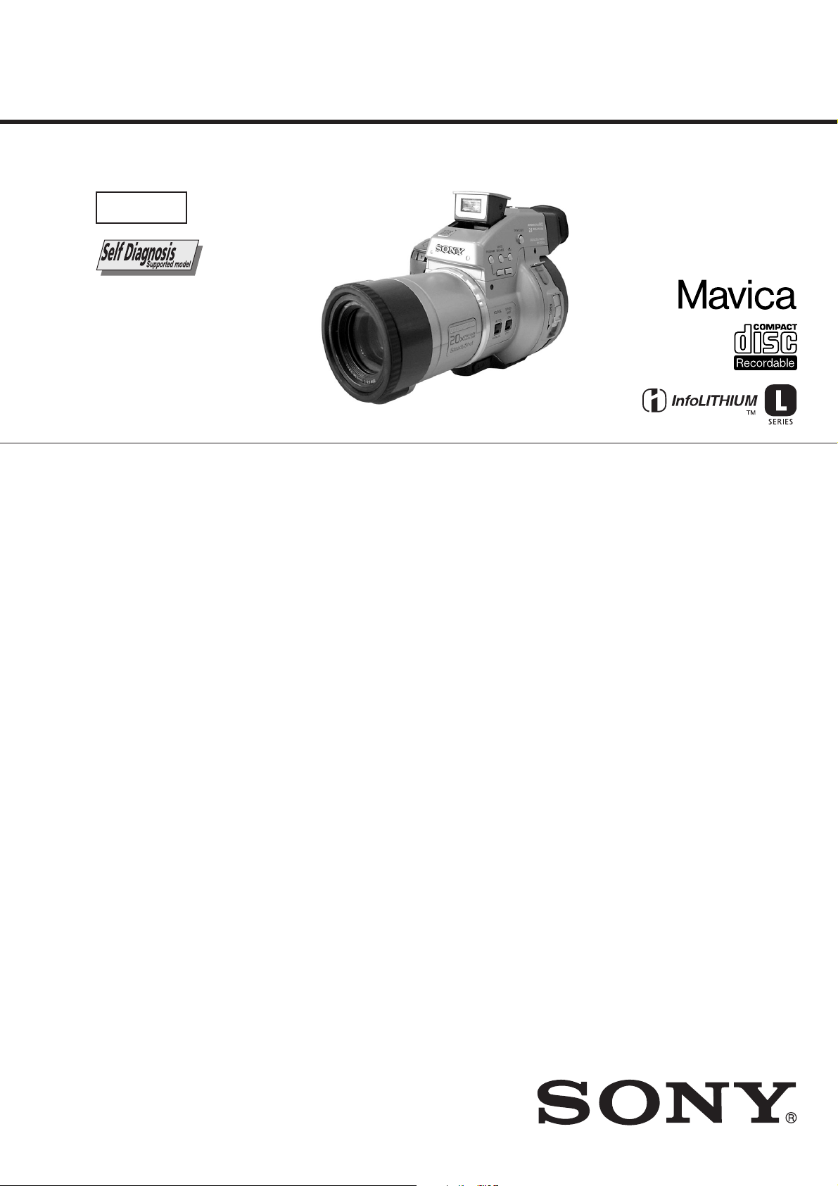
MVC-CD1000
SERVICE MANUAL
Level 1
Ver 1.0 2000. 07
SPECIFICATIONS
System
Image device
1/2.7 type color CCD
Lens
10× zoom lens
f = 1/4 – 2 3/8 in (6.0 –
60.0 mm) (1 9/16 – 15 3/8 in
(39 – 390 mm) when
converted into a 35 mm still
camera)
F = 2.8
Exposure control
Automatic exposure
White balan ce
Automatic, Indoor, Outdoor,
One-push
Data compression
system
Movie: MPEG1
Still:
JPEG, TIFF, GIF (in TEXT
mode)
Audio (with still im age):
MPEG AUDIO (Monaural)
Recording medium
8 cm CD-R
Flash
Recommended recording
distance:
23 5/8 in to 8 1/3 feet (0.6 m
to 2.5 m)
Drive
Read: Maximum ×8
Write: × 4
Readout
Noncontact optical readout
(using semiconductor laser)
Laser
Wa velength: 777 to 787 nm
NA: 0.5
Maximum output: 23 mW
Emission duration: 600 ns
Input and Output
connector
A/V OUT (MONO) jack
(Monaural)
Minijack Video:
1 Vp-p, 75Ω , unbalanced,
sync negative
Audio: 327 mV (at a 47 kΩ
load)
Output impedance: 2.2 k
DIGITAL I/O jack
4-pin connector
External flash jack
Minijack
LCD screen
LCD panel
TFT (Thin Film Transistor
active matrix) drive
LCD size
2.5 type
T otal number of dots
123 200 (560×220) dots
Viewfinder
LCD panel
TFT (Thin Film Transistor
active matrix) drive
T otal number of dots
180 000 (800×225) dots
General
Application
Sony battery pack NP-F550
Power requirements
8.4 V
Power consumption
(During shooting)
4.9 W (When using the LCD
screen)
4.5 W (When u sing the
viewfinder)
Operation temperature
32 °F to 104 °F (0 °C t o
40 °C)
Ω
Storage te m p erature
–4 °F to +140 °F (–20 °C to
+60 °C)
Maximum dimensions
5 1/2×5 1/4×8 3/8 in
(137×131×212 mm) (w/ h/d)
Mass
Approx. 35 oz (990 g)
(including battery, disc and
lens cap, etc.)
Built-in microphone
Electret condenser
microphone
Built-in speaker
Dynamic speaker
AC-L10A/L10B/L10C
AC power adaptor
Power requirements
100 V to 240 V AC,
50/60 Hz
Rated output voltage
DC 8.4 V, 1.5 A in operating
mode
Operation temperature
32 °F to 104 °F (0 °C to
40°C)
Storage temperature
–4 °F to +140 °F (–20 °C to
+60 °C)
Maximum dimensions
5×1 9/16×2 1/2 in
(125×39×62 mm) (w/h/d)
Mass
Approx. 10 oz (280 g)
NP-F550 battery pack
Used battery
Lithium ion battery
Maximum vo ltage
DC 8.4 V
Nominal voltage
DC 7.2 V
Capacity
10.8 Wh (1 500 mAh)
AEP Model
UK Model
Accessories
AC-L10A/L10B/L10C
AC power adaptor (1)
Power cord (mains lead) (1)
NP-F550 battery pack (1)
A/V connecting cable (1)
USB cable (1 )
8 cm CD adaptor (1)
Mavica disc (5)
Shoulder strap (1)
Lens cap (1)
Lens cap strap (1)
CD-ROM (3)
Operating instructions (3)
Design and specifications
are subject to change
without notice.
DIGITAL STILL CAMERA
Page 2

TABLE OF CONTENTS
SERVICE NOTE ····································································· 3
1. MAIN PARTS
1. ORNAMENTAL PARTS ····················································5
2. DISASSEMBLY ································································· 7
2-1. LCD SECTION (PK-051 BOARD) ··································· 7
2-2. CABINET (UPPER) SECTION········································· 8
2-3. FLASH UNIT····································································· 8
2-4. EVF SECTION··································································· 9
2-5. CABINET (F) SECTION,
CABINET (CENTER) SECTION······································ 9
2-6. LENS BLOCK ASSEMBLY,
CONTROL SWITCH BLOCK (FS52K),
CONTROL SWITCH BLOCK (JK52K) ························· 10
2-7. CONTROL SWITCH BLOCK (ZM52K)························ 10
2-8. VP-051, SE-115 BOARDS ·············································· 10
2-9. SY -060, VC-246 BOARDS ·············································· 11
2-10. MECHANISM DECK (DDX-G2000 COMPLETE
ASSEMBLY), CONTROL SWITCH BLOCK (AJ52K) ·· 11
2-11. LID CABINET SECTION,
CONTROL SWITCH BLOCK (MP52K) ························ 12
3. REPAIR PARTS LIST ······················································ 13
3-1. EXPLODED VIEWS ·······················································13
3-1-1.OVERALL SECTION······················································ 13
3-1-2.CABINET (UPPER) SECTION······································· 14
3-1-3.EVF SECTION································································· 15
3-1-4.CABINET (F) SECTION ················································· 16
3-1-5.LENS SECTION ······························································ 17
3-1-6.CABINET (CENTER) SECTION···································· 18
3-1-7.LID CABINET SECTION ··············································· 19
2. GENERAL
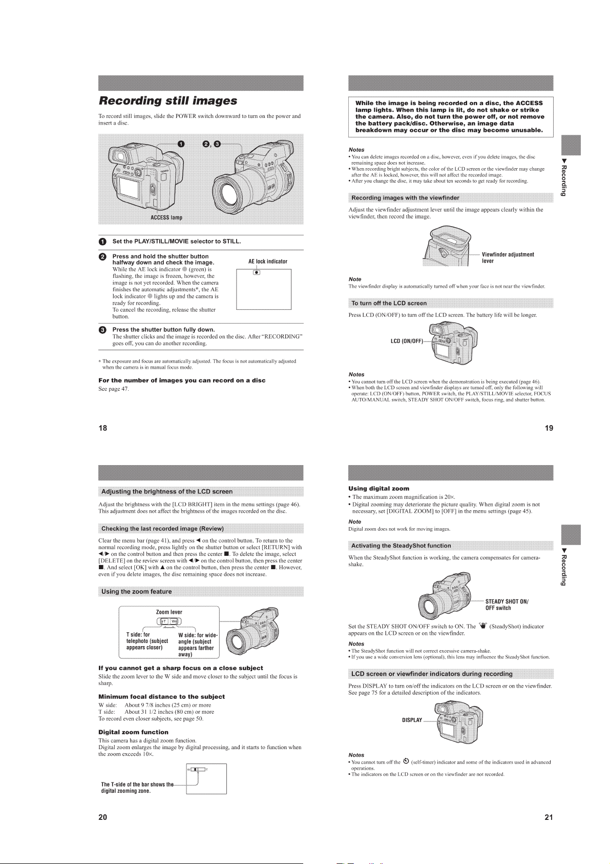
Getting started
Identifying the parts ································································ 20
Preparing the power supply ···················································· 20
Setting the date and time························································· 21
Inserting a disc ········································································ 22
Basic operations
B Recording
Initializing a disc (INITIALIZE) ············································ 22
Recording still images ···························································· 23
Recording moving images ······················································ 24
B Playback
Playing back still images ························································ 24
Playing back moving images ·················································· 25
Viewing images using a personal computer ···························25
Image file storage destinations and image file names ············ 28
Advanced operations
Before performing advanced operations
How to use the PLAY/STILL/MOVIE selector······················ 28
How to use the control button················································· 28
How to change the menu settings ··········································· 29
B V arious recording
Setting the image size (IMAGE SIZE) ··································· 30
Recording still images for e-mail (E-MAIL)·························· 30
Adding audio files to still images (VOICE) ···························30
Recording text documents (TEXT) ········································30
Recording uncompressed images (TIFF)································ 30
Recording images in macro ···················································· 31
Focusing manually·································································· 31
Using the PROGRAM AE function ········································ 31
Using the Spot light–metering function·································· 31
Adjusting the exposure (EXPOSURE) ··································· 31
Adjusting the white balance (WHITE BALANCE) ··············· 31
Recording the date and time on the still image (DATE/TIME) ··
Enjoying picture effects (PICTURE EFFECT) ······················ 32
B V arious playback
Playing back six images at once (INDEX) ····························· 32
Enlarging a part of the still image (Zoom and trimming)······· 32
Rotating a still image (ROTATE)············································ 33
Playing back the still images in order (SLIDE SHOW) ········· 33
Viewing images on a TV screen ············································· 33
B Editing
Preventing accidental erasure (PROTECT) ···························· 33
Deleting images (DELETE) ···················································33
Changing the recorded still image size (RESIZE)·················· 34
Selecting still images to print (PRINT MARK) ····················· 34
Additional information
Precautions·············································································· 34
On discs ··················································································35
Using your camera abroad ······················································ 35
Troubleshooting ······································································ 35
Warning and notice messages ················································· 36
Self-diagnosis display ····························································· 36
LCD screen/viewfinder indicators ·········································· 37
32
SAFETY-RELATED COMPONENT WARNING!!
COMPONENTS IDENTIFIED BY MARK 0 OR DOTTED LINE WITH
MARK 0 ON THE SCHEMATIC DIAGRAMS AND IN THE PARTS
LIST ARE CRITICAL TO SAFE OPERATION. REPLACE THESE
COMPONENTS WITH SONY PARTS WHOSE PART NUMBERS
APPEAR AS SHOWN IN THIS MANUAL OR IN SUPPLEMENTS
PUBLISHED BY SONY.
SAFETY CHECK-OUT
After correcting the original service problem, perform the following
safety checks before releasing the set to the customer.
1. Check the area of your repair for unsoldered or poorly-soldered
connections. Check the entire board surface for solder splashes
and bridges.
2. Check the interboard wiring to ensure that no wires are
"pinched" or contact high-wattage resistors.
3. Look for unauthorized replacement parts, particularly
transistors, that were installed during a previous repair . Point
them out to the customer and recommend their replacement.
4. Look for parts which, through functioning, show obvious signs
of deterioration. Point them out to the customer and
recommend their replacement.
5. Check the B+ voltage to see it is at the values specified.
6. Flexible Circuit Board Repairing
• Keep the temperature of the soldering iron around 270˚C
during repairing.
• Do not touch the soldering iron on the same conductor of the
circuit board (within 3 times).
• Be careful not to apply force on the conductor when soldering
or unsoldering.
— 2 —
Page 3

• NOTE FOR REPAIR
r
SERVICE NOTE
Make sure that the flat cable and flexible board are not cracked of
bent at the terminal.
Do not insert the cable insufficiently nor crookedly.
Cut and remove the part of gilt
which comes off at the point.
(Take care that there are
some pieces of gilt left inside)
When remove a connector, don't pull at wire of connector.
Be in danger of the snapping of a wire.
When installing a connector, don't press down at wire of connector.
Be in danger of the snapping of a wire.
[Discharging of the FLASH unit’s charging capacitor]
The charging capacitor of the FLASH unit is charged up to the
maximum 300 V potential.
There is a danger of electric shock by this high voltage when the
capacitor is handled by hand. The electric shock is caused by the
charged voltage which is kept without discharging when the main
power of the MVC-CD1000 is simply turned off. Therefore, the
remaining voltage must be discharged as described below.
Preparing the Short Jig
To preparing the short jig. a small clip is attached to each end of a
resistor of 1 kΩ /1 W (1-215-869-11)
Wrap insulating tape fully around the leads of the resistor to prevent
electrical shock.
1 kΩ/1 W
Wrap insulating tape.
Discharging the Capacitor
Short circuits between the positive and the negative terminals of
charged capacitor with the short jig about 10 seconds.
Capacito
Short jig
— 3 —
Page 4

[Description on Self-diagnosis Display]
Self-diagnosis display
• C: ss: ss
The contents which can be handled
by customer, are displayed.
• E: ss: ss
The contents which can be handled
by engineer, are displayed.
Display Code
C:32:01
C:13:01
E:91:01
*1
E:61:00
*1
E:61:10
Note: The error code is cleared if rthe battery is removed, except
defective flash, unit.
*1 : The error display is given in two ways.
*2 : When the flash charging failed, Page:D, Address:67, Data:04
are written.
After repair, be sure to write Page:D, Address:67, Data:00.
Change the disk and turn off the main
power then back on.
Replace the CD-R disk.
Checking of flash unit or replacement of
flash unit
Checking of lens drive circuit
Countermeasure
Defective base unit.
• The type of CD-R disk that cannot be
• Data is damaged.
*2
Abnormality when flash is being
charged.
When failed in the focus initialization.
Cause
used by this machine, is inserted.
Caution Display During Error
DRIVE ERROR
DISK ERROR
Flash LED
Flash display
Flashing at 3.2 Hz
—
— 4 —
Page 5
1. MAIN PARTS
Note:
• Follow the disassembly procedure in the numerical order given.
• Items marked “*” are not stocked since they are seldom required for routine service.
Some delay should be anticipated when ordering these items.
• The parts numbers of such as a cabinet are also appeared in this section.
Refer to the parts number mentioned below the name of parts to order.
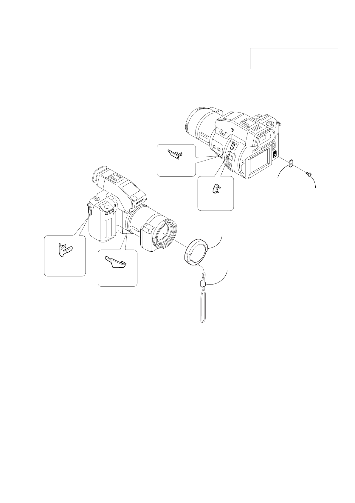
1. ORNAMENTAL PARTS
AV cover
3-062-365-01
ACC jack lid
3-062-428-01
MVC-CD1000
The components identified by mark 0 or
dotted line with mark 0 are critical for safety.
Replace only with part number specified.
CPC jack lid
3-062-407-01
Tapping
screw (B2 × 5)
3-948-339-01
DC jack lid
3-062-427-01
Lens cap assembly
X-3950-691-1
Cap string
3-062-043-01
USB cover
3-062-364-01
— 5 —
Page 6
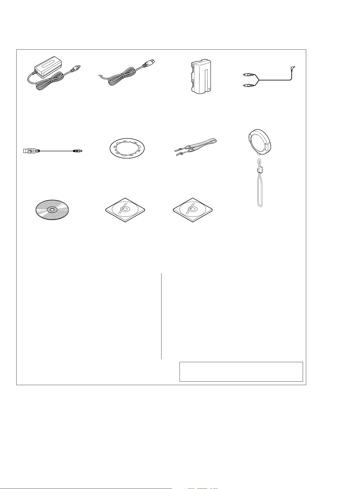
Checking supplied accessories
)
AC-L10A AC power adaptor (1)
0
1-475-599-11
USB cable (1)
1-792-623-21
Application software:
Picture Gear 4.1Lite
(System Disc)(CD ROM) (1)
3-060-476-01
Power cord (main lead)(1) (AEP model)
0
1-769-608-11
Power cord (main lead)(with filter)(1)
(UK model)
0
1-783-374-11
8cm CD adaptor (1)
3-063-085-01
Bundle soft (2000) (1)
3-060-716-01
Other accessories
3-060-457-11 MANUAL, INSTRUCTION (PICTURE GEAR 4.1 LITE)
3-060-458-11 MANUAL, INSTRUCTION (PICTURE GEAR 4.1 LITE)
(ENGLISH/RUSSIAN)(AEP)
3-060-458-21 MANUAL, INSTRUCTION (PICTURE GEAR 4.1 LITE)
(FRENCH/GERMAN)(AEP)
3-060-458-31 MANUAL, INSTRUCTION (PICTURE GEAR 4.1 LITE)
3-060-458-41 MANUAL, INSTRUCTION (PICTURE GEAR 4.1 LITE)
(SPANISH/PORTUGUESE)(AEP)
3-060-458-51 MANUAL, INSTRUCTION (PICTURE GEAR 4.1 LITE)
(POLISH/SWEDISH)(AEP)
(ENGLISH)(UK)
(ITALIAN/DUTCH)(AEP)
NP-F550 battery pack (1)
Not supplied
Shoulder belt (S) (1)
3-987-015-01
SPV-001 (12cm CD)(1)
3-063-034-01
3-062-473-11 MANUAL, INSTRUCTION (ENGLISH)
3-062-473-21 MANUAL, INSTRUCTION (FRENCH/GERMAN)(AEP)
3-062-473-31 MANUAL, INSTRUCTION (SPANISH/PORTUGUESE)(AEP)
3-062-473-41 MANUAL, INSTRUCTION (ITALIAN/DUTCH)(AEP)
3-062-473-61 MANUAL, INSTRUCTION (SWEDISH/RUSSIAN)(AEP)
3-062-474-11 MANUAL, INSTRUCTION (DIRECT CD)(ENGLISH)
3-062-474-21 MANUAL, INSTRUCTION (DIRECT CD)(FRENCH/GERMAN)
3-062-474-31 MANUAL, INSTRUCTION (DIRECT CD)
3-062-474-41 MANUAL, INSTRUCTION (DIRECT CD)(ITALIAN/DUTCH)
3-062-474-61 MANUAL, INSTRUCTION (DIRECT CD)
Note : The components identified by mark 0 or dotted
line with mark 0 are critical for safety.
Replace only with part number specified.
A/V connecting cable (1.5m)(1)
1-783-738-31
(Fig. A
(Fig. B)
(Fig. A) Lens cap (1)
X-3950-691-1
(Fig. B) Lens cap strap (1)
3-062-043-01
Mavica disc (5)
Not supplied
(AEP)
(SPANISH/PORTUGUESE)(AEP)
(AEP)
(SWEDISH/RUSSIAN)(AEP)
— 6 —
Page 7

2. DISASSEMBLY
MVC-CD1000
2-2. Cabinet (upper) section
2-6. Lens block assembly, Control switch block (FS52K),
Control switch block (JK52K)
2-7. Control switch block (ZM52K)
2-1. LCD section (PK-051 board)
2-5. Cabinet (F) section, Cabinet (center) section
2-8. VP-051, SE-115 boards
2-3. Flash unit
2-4. EVF section
2-9. SY-060, VC-246 boards
2-10. Mechanism deck (DDX-G2000 complete assembly),
Control switch block (AJ52K)
2-11. Lid cabinet section,
Control switch block (MP52K)
PK-051
Board
B
A
A
B
1
T wo tapping
screws (B2 × 5)
2
T apping screw
(B2 × 5)
5
Four tapping
screws (B2 × 5)
3
Six tapping
screws (B2 × 5)
2
Hinge shaft
stopper
5
Tilt up the upper
hinge assembly
in the direction
of the arrow.
Remove the lid rear lid
in the direction of the arrow.
6
Lid rear lid
Lid rear lid
7
Lock plate
8
Peep window
4
Screw (M2 × 3),
lock ace, p2
6
Two screws
(M2 × 3), lock ace, p2
7
BL support
assembly
8
PK-051 board
1
Control switch block
(LC52K) (4P)
3
Control switch block
(LC52K)
4
FP-046 flexible
board (24P)
9
Liquid crystal
indicator module
q;
Back light
Cold cathode
fluorescent tube
The following flow chart shows the disassembly procedure.
NOTE: F ollo w the disassembly procedure in the numerical order given.
2-1. LCD SECTION (PK-051 BOARD)
— 7 —
Page 8

2-2. CABINET (UPPER) SECTION
d
Note: The built-in charging capacitor inside the FLASH unit is charged to the maximum of 300V.
There is a danger of electric shock due to the high voltage when the capacitor is tached by bare hand.
Discharge the voltage remained in the capacitor, referring to the Service Note (See page 3).
6
FP-041 flexible
board (25P)
4
Control switch block
(AE52K) (6P)
1
Screw (M2 × 5),
lock ace, p2
Note
7
(upper) section
Cabinet
5
Flash unit
(10P)
3
T wo screws
(M2 × 5),
lock ace, p2
2
Screw (M2 × 5),
lock ace, p2
2-3. FLASH UNIT
Note: The built-in charging capacitor inside the FLASH unit is charged to the maximum of 300V.
There is a danger of electric shock due to the high voltage when the capacitor is tached by bare hand.
Discharge the voltage remained in the capacitor, referring to the Service Note (See page 3).
2
4
Control switch
block (AE52K)
3
Two
dowels
5
AE button
6
Push the
button to open
the flash unit
9
Stroboscope
blind plate
qd
Stroboscope
luminous case
qa
Screw
(M2 × 3),
lock ace, p2
T apping
screw
(B2 × 5)
Note
1
Microphone
(2P)
qf
qs
Screw
(M2 × 3),
lock ace, p2
7
T wo tapping
screws (B2 × 5)
q;
Screw (M2 × 3),
lock ace, p2
Pull
Note
Be careful that
the flash must
not be caught.
PRECAUTION
DURING
INSTALLATION
8
7
Three tapping
6
screws (B2 × 5)
1
T wo tapping
screws (B2 × 5)
2
Screw
(M2 × 3),
lock ace, p2
4
5
Hard steel
light guide
cap
3
Screw
(M2 × 3),
lock ace, p2
PRECAUTION DURING
INSTALLATION
Switch
position
2
Screw
(M2 × 3),
lock ace, p2
1
T apping
screw
(B2 × 5)
4
Two S shiel
plates
5
Flash unit
3
Stroboscope
base assembly
Attaching harnesses of the
Flash unit
Harness (Flash)
8
Stroboscope lid
Tape
Ray catcher
element
— 8 —
Page 9

2-4. EVF SECTION
1
Screw
(M2 × 5),
lock ace, p2
2
T apping
screw
(B2 × 5)
4
EVF section
3
T wo tapping
screws (B2 × 5)
qa
assembly (453)
9
claws
qs
Cover the cushion and
diffusion plate with a piece
of paper or adhesive tape
or the like so that the parts
must not be scattered.
5
MK-015 board
2
VF cabinet (rear) assembly
4
VF lens
Three
-1
F
V
6
Three claws
VF cabinet (upper)
3
Two claws
q;
LB-066 board
8
VF cabinet (lower)
assembly
1
T wo tapping
screws (M1.7 × 4)
4
4
7
VF-144 board
2-5. CABINET (F) SECTION, CABINET (CENTER) SECTION
9
qf
Cabinet (center)
section
Two screws (M2 × 5),
lock ace, p2
SY 060
qa
T wo screws
(M2
×
5),
lock ace, p2
6
FP-040 flexible board (22P)
3
Flexible board (from lens assembly)(26P)
4
Ferrite core and F adhesive sheet
qs
q;
lock ace, p2
Screw (M2 × 5), lock ace, p2
7
Battery terminal board (4P)
8
Control switch block (ZM52K) (6P)
2
Control switch block (FS52K) (4P)
1
Control switch block (JK52K) (8P)
5
FP-044 flexible board (18P)
Two screws (M2 × 5),
qd
Cabinet (F) section
— 9 —
Page 10

2-6. LENS BLOCK ASSEMBLY, CONTROL SWITCH BLOCK (FS52K),
s
CONTROL SWITCH BLOCK (JK52K)
6
2
Lens block assembly
4
5
Control switch
T ape
3
Lens ring
T wo screws
(M2
lock ace, p2
block (FS52K)
2-7. CONTROL SWITCH BLOCK (ZM52K)
PRECAUTION
DURING INSTALLATION
2
T wo tapping
screws K1 (B2
×
5)
When installing it,
align the switch position
as shown.
×
3),
7
Control switch
block (JK52K)
1
Four screw
(+PS 2 × 8)
3
Hinge retainer
1
4
Battery lid
2-8. VP-051, SE-115 BOARDS
7
Lens cabinet
(upper) assembly
4
FP-043 flexible
board (8P)
1
Screw (M2 × 5),
lock ace, p2
5
Lens cabinet (VP)
assembly and
MF block
B
Control switch
block (ZM52K),
Switch holder
A
B
8
Three tapping
screws (B2
qa
T apping
screw
×
5)
6
Four claws
(B2
7
BT lock claw
The claws can be released easily
B
by pressing portion
×
5)
at the same time.
6
qs
Control switch
block (ZM52K)
q;
Ground plate (ZM)
9
T apping
screw (B2
8
Battery terminal board,
×
5)
Battery holder,
Hinge holder assembly,
etc
5
Three tapping
screws (B2
×
5)
A
3
Remove the two claws
(Remove it while taking
care as the FP-043 flexible
board is connected.)
9
Lens cabinet
(lower) assembly
CD272
2
screw (B2
— 10 —
q;
T apping
4
Two claws
5
VP-051 board
×
5)
2
Screw
×
SE-115 board
1
Three screws
×
(M2
3),
lock ace, p2
3),
VP-051
CD272
3
(M2
lock ace, p2
Page 11

2-9. SY-060, VC-246 BOARDS
2
MD082
SY 060
MD-082
Board
MD-082
Board
1
1
2
Screw
(M2
×
5),
lock ace, p2
2
T wo screws
(M2
×
3),
lock ace, p2
5
Screw
(M2 × 5),
lock ace, p2
3
Screw
(M2
×
5),
lock ace, p2
4
Screw
(M2 × 5),
lock ace, p2
6
Mechanism deck
DDX-G2000
complete assembly
4
T wo tapping
screws (B2 × 5)
5
T wo tapping
screws (B2 × 5)
6
Strap plate (L)
2
T wo tapping
screws (B2
×
5)
3
Open leaf spring
7
Control switch block
(AJ52K)
3
Board to board
connector (50P)
5
SY-060, VC-246 boards
4
Claw
1
Control switch block
(AJ52K) (8P)
Precautions during handling
• Do not turn the side of the optical lens downward.
• Hold the frame.
• Do not touch the optical lens surface.
q;
Claw
MD082
4
Control switch block
(AJ52K) (8P)
9
Board to board
connector (50P)
qa
VC-246 board
8
SY frame (B)
SY 060
1
Three screws
(M2
×
3),
lock ace, p2
7
T wo screws
(M2 × 3),
lock ace, p2
6
SY frame (A)
VC246
SY 060
2
connector (80P)
3
SY-060 board
5
T wo screws
(M2
×
3), lock ace, p
Board to board
2-10. MECHANISM DECK (DDX-G2000 COMPLETE ASSEMBLY), CONTROL SWITCH BLOCK (AJ52K)
— 11 —
Page 12

2-11. LID CABINET SECTION, CONTROL SWITCH BLOCK (MP52K)
8
Two hinge shafts
7
6
Hinge shaft stopper
2
Two
claws
3
Flexible guide
5
Two claws
1
T wo tapping
screws (B2 × 5)
4
T wo tapping
screws (B2 × 5)
PRECAUTION
DURING INSTALLATION
When installing it,
align the switch position
as shown.
qa
Lid cabinet section
9
Screw (M2 × 3),
lock ace, p2
q;
Screw (M2 × 3),
lock ace, p2
5
Strap plate (R)
1
Extension coil
spring (lid)
3
Spring plate
6
DC-IN
connector
q;
Control switch block
(MP52K)
4
T wo tapping
screws (B2 × 5)
9
T apping
screw (B2 × 5)
8
Damper holder
7
T apping
screw (B2 × 5)
2
T apping
screw (B2 × 5)
— 12 —
Page 13

3. REPAIR PARTS LIST
3-1. EXPLODED VIEWS
NOTE:
• -XX, -X mean standardized parts, so they may
have some differences from the original one.
• Items marked “*” are not stocked since they
are seldom required for routine service. Some
delay should be anticipated when ordering these
items.
3-1-1. OVERALL SECTION
• The mechanical parts with no reference number
in the exploded views are not supplied.
The components identified by mark 0 or
dotted line with mark 0 are critical for safety.
Replace only with part number specified.
Cabinet (center) section
(See page 18)
1
C
1
2
11
F
1
D
5
B
14
1
13
Cabinet (upper) section
(See page 14)
4
E
1
6
-246
C
V
7
5
A
9
18
SY-
8
060
E
10
F
12
8
17
C
D
B
A
1
15
1
1
(Note)
3
M
B
D
oard
-082
1
1
2
1
Cabinet (F) section
(See page 16)
2
16
: BT401(Lithium battary) VC board on the mount position.
Note: When handling this part, refer to “Disassembly” Section 2-10 [MECHANISM DECK (DDX-G2000 COMPLETE ASSEMBLY),
CONTROL SWITCH BLOCK (AJ52K)] on page 11.
Ref. No. Part No. Description Remarks Ref. No. Part No. Description Remarks
1 3-968-729-31 SCREW (M2), LOCK ACE, P2
2 3-948-339-01 SCREW, TAPPING
3 not supplied DDX-G2000 COMPLETE ASSY (FOR SERVICE)
* 4 3-062-403-01 FRAME (A), SY
5 3-062-992-01 PLATE, VC SHIELD
6 not supplied VC-246 BOARD, COMPLETE (FOR SERVICE)
* 7 3-062-404-01 FRAME (B), SY
8 3-968-729-51 SCREW (M2), LOCK ACE, P2
9 1-678-237-21 CC-102 FLEXIBLE BOARD
10 not supplied SY-060 BOARD, COMPLETE (FOR SERVICE)
11 3-062-407-01 LID,CPC JACK
12 1-678-230-12 FP-040 FLEXIBLE BOARD
13 3-724-511-31 SHOE, ACCESSORY
14 3-063-356-01 SCREW (2X3.5)
15 X-3950-691-1 CAP ASSY, LENS
16 3-062-043-01 STRING, CAP
17 1-500-294-11 CORE, FERRITE
* 18 3-063-953-01 SHEET, F ADHESIVE
— 13 —
Page 14

3-1-2. CABINET (UPPER) SECTION
F
54
H
54
54
EVF section
G
(See page 15)
B
A
I
54
55
H
F
G
56
C
59
A
72
B
73
55
65
53
67
53
not
supplied
not
supplied
52
not
supplied
54
57
D
58
(Note)
63
63
54
68
D
63
66
63
E
54
51
71
I
not
supplied
54
Note: The built-in charging capacitor inside the FLASH unit is charged to the maximum of 300V.
There is a danger of electric shock due to the high voltage when the capacitor is tached by bare hand.
Discharge the voltage remained in the capacitor, referring to the Service Note (See page 3).
60
61
62
64
MIC901
C
E
54
69
70
Ref. No. Part No. Description Remarks Ref. No. Part No. Description Remarks
51 X-3950-788-1 CASE ASSY, LUMINOUS
52 X-3950-789-1 FRAME ASSY, SHOE
53 3-968-729-61 SCREW (M2X3), LOCK ACE, P2
54 3-948-339-01 SCREW, TAPPING
55 3-968-729-31 SCREW (M2), LOCK ACE, P2
56 X-3950-787-1 CABINET (UPPER) ASSY
057 not supplied FLASH UNIT
58 X-3950-790-1 BASE ASSY, STROBOSCOPE
59 3-062-439-01 LID,STROBOSCOPE
60 3-062-434-01 RUBBER, MICROPHONE
61 3-062-433-01 GRILLE, MICROPHONE
62 3-062-442-01 SPONGE, MICROPHONE
— 14 —
63 3-968-729-51 SCREW (M2), LOCK ACE, P2
64 3-062-440-01 FRAME, MICROPHONE
65 3-062-435-01 RETAINER, MICROPHONE
66 3-062-436-01 CAP,HARD STEEL LIGHT GUIDE
67 3-062-437-01 HOLDER, HARD STEEL
68 3-062-438-01 PLATE, TALLY LIGHT GUIDE
69 3-062-441-01 BUTTON, AE
70 1-476-050-11 SWITCH BLOCK, CONTROL (AE52K)
71 3-062-991-01 PLATE, S SHIELD
72 3-064-534-01 SEAL(S), ELECTROSTATIC
73 3-062-299-01 SHEET, MICROPHONE
MIC901 1-542-312-11 MICROPHONE
Note : The components identified by mark 0 or dotted
line with mark 0 are critical for safety.
Replace only with part number specified.
Page 15

3-1-3. EVF SECTION
111
110
LCD902
108
109
105
112
114
108
104
113
107
106
103
VF-144
102
101
Ref. No. Part No. Description Remarks Ref. No. Part No. Description Remarks
101 1-678-231-11 FP-041 FLEXIBLE BOARD
102 not supplied VF-144 BOARD, COMPLETE
103 3-713-791-01 SCREW (M1.7X4), TAPPING, P2
104 X-3950-793-1 CABINET (LOWER) ASSY, VF
105 not supplied MK-015 BOARD, COMPLETE
106 1-678-232-11 FP-042 FLEXIBLE BOARD
107 not supplied LB-066 BOARD, COMPLETE
108 not supplied CUSHION (455), LCD
109 not supplied ILLUMINATOR (455), BL
110 not supplied CUSHION (1), LCD
111 X-3949-883-1 LENS ASSY (453), VF
112 X-3950-792-1 CABINET (REAR) ASSY, VF
113 3-062-463-01 CABINET (UPPER), VF
* 114 not supplied SPACER, LCD
LCD902 not supplied LCX027AK-J
— 15 —
Page 16

3-1-4. CABINET (F) SECTION
Lens section
(See page 17)
158
160
(Note)
161
166
168
not
supplied
154
162
163
159
155
156
151
157
153
153
165
167
157
164
174
not
supplied
172
not supplied
170
153
Note: When attaching this part, refer to “Disassembly” Section 2-7 [CONTROL SWITCH BLOCK (ZM52K)]
on page 10 to perform positioning.
153
BT901
169
not
supplied
171
153
173
Ref. No. Part No. Description Remarks Ref. No. Part No. Description Remarks
151 X-3950-778-1 CABINET (F) ASSY
153 3-948-339-01 SCREW, TAPPING
154 3-062-360-01 CABINET (C)
155 3-062-365-01 COVER, AV
156 3-062-364-01 COVER, USB
157 3-968-729-51 SCREW (M2), LOCK ACE, P2
158 1-476-054-11 SWITCH BLOCK, CONTROL (FS52K)
159 3-062-347-01 RING, LENS
160 3-062-346-01 CABINET (D)
161 not supplied SWITCH BLOCK, CONTROL (ZM52K)
162 3-062-345-01 HOLDER, SWITCH
163 3-062-349-01 PLATE (ZM), GROUND
164 1-476-048-11 SWITCH BLOCK, CONTROL (JK52K)
165 7-628-253-35 SCREW +PS 2X8
166 3-969-380-11 SPRING, BATTERY
167 3-052-574-01 CLAW, BT LOCK
* 168 3-058-746-01 HOLDER, BATTERY
169 X-3950-779-1 LID ASSY, BATTERY
170 3-736-363-41 TAPPING
171 X-3950-246-1 HOLDER ASSY, HINGE
172 3-058-802-01 SPRING, B LOCK
173 3-058-748-01 KNOB, B LOCK
174 3-062-348-01 SCREW, TRIPOD
BT901 1-694-297-21 TERMINAL BOARD, BATTERY
— 16 —
Page 17

3-1-5. LENS SECTION
213
214
215
216
211
B
Screw, tapping
A
212
210
D
209
208
207
208
E
206
IC101
205
not
supplied
208
E
208
227
202
224
208
201
A
225
B
226
VP-051
217
223
218
222
not
supplied
C
222
203
204
not
supplied
D
220
221
208
C
219
Ref. No. Part No. Description Remarks Ref. No. Part No. Description Remarks
201 3-947-268-11 TITE (2), +B TAPPING (P)
202 not supplied CD-272 BOARD, COMPLETE
203 1-678-228-11 FP-038 FLEXIBLE BOARD
204 3-968-729-31 SCREW (M2), LOCK ACE, P2
205 not supplied RUBBER (CL), SEAL
206 not supplied FILTER BLOCK, OPTICAL
207 not supplied ADAPTOR (CL), CCD FITTING
208 3-948-339-01 SCREW, TAPPING
209 X-3950-776-1 CABINET (LOWER) ASSY, LENS
210 not supplied LENS ASSY
211 not supplied VAP ASSY
212 X-3950-775-1 CABINET (UPPER) ASSY, LENS
213 X-3950-777-1 CABINET (VP) ASSY, LENS
214 3-965-060-01 PIN, MF FIXED
215 3-965-098-01 SCREW
216 3-062-356-01 RUBBER, MF
217 3-062-355-01 RING, MF
218 3-062-357-01 FOOT (LENS), RUBBER
219 1-418-068-11 MF BLOCK
220 1-678-233-11 FP-043 FLEXIBLE BOARD
221 1-678-234-11 FP-044 FLEXIBLE BOARD
222 3-968-729-51 SCREW (M2), LOCK ACE, P2
223 not supplied SE-115 BOARD, COMPLETE
224 3-062-350-01 FRAME, LENS
225 1-678-229-11 FP-039 FLEXIBLE BOARD
226 not supplied VP-051 BOARD, COMPLETE
* 227 not supplied HEAT SINK, CD
IC101 not supplied CCD BLOCK ASSY (CCD IMAGER)
— 17 —
Page 18

3-1-6. CABINET (CENTER) SECTION
284
257
F
Lid cabinet section
(See page 19)
C
A
D
B
B
A
276
E
271
272
273
270
not
supplied
E
269
260
268
267
C
D
261
266
264
263
265
262
(Note)
281
278
274
279
280
F
282
255
254
256
251
259
258
J901
251
285
275
257
251
252
253
251
Note: When attaching this part, refer to “Disassembly” Section 2-11 [LID CABINET SECTION, CONTROL
SWITCH BLOCK (MP52K)] on page 12 to perform positioning.
251
277
251
283
251
Ref. No. Part No. Description Remarks Ref. No. Part No. Description Remarks
251 3-948-339-01 SCREW, TAPPING
252 3-062-408-01 GUIDE, FLEXIBLE
253 3-062-410-01 HOLDER, DAMPER
254 1-476-047-11 SWITCH BLOCK, CONTROL (MP52K)
255 3-062-406-01 PLATE (R), STRAP
256 3-053-141-01 SPRING, POWER
257 3-968-729-61 SCREW (M2X3), LOCK ACE, P2
258 X-3950-785-1 CABINET (CENTER) ASSY
259 3-355-424-21 SCREW, TAPPING
260 3-054-990-01 SLEEVE
261 3-051-124-01 FOOT, RUBBER
262 X-3950-784-1 LOCK ASSY, LID
263 3-062-423-01 SPRING, COMPRESSION
264 3-062-420-01 GUIDE, LOCK LEVER
265 3-062-421-01 LEVER, STOPPER
266 3-062-419-01 LEVER, LOCK
267 3-062-422-01 SLIDER, STOPPER
268 3-062-428-01 LID, ACC JACK
269 3-062-424-01 LEVER, MODE
270 X-3946-488-1 SPRING ASSY, AE LEAF
271 3-052-536-02 BUTTON, POWER
272 3-062-427-01 LID, DC JACK
273 3-062-425-01 HOLDER, POWER BUTTON
274 3-948-339-41 SCREW, TAPPING
275 3-062-343-01 SHAFT, HINGE
276 3-062-344-01 STOPPER, HINGE SHAFT
277 3-062-409-01 SPRING, OPEN LEAF
278 1-476-049-11 SWITCH BLOCK, CONTROL (AJ52K)
279 3-062-405-01 PLATE (L), STRAP
280 3-968-729-31 SCREW (M2), LOCK ACE, P2
* 281 3-064-541-01 SHEET, GROUND
282 3-063-841-01 SPRING (LID), EXTENSION COIL
283 3-063-840-01 PLATE, SPRING
284 3-063-845-01 SPRING (B), OPEN PLATE
* 285 3-064-356-01 FILM, ELECTROSTATIC
J901 1-794-045-41 CONNECTOR, DC-IN
— 18 —
Page 19

3-1-7. LID CABINET SECTION
PK-051
Board
SW
-342
A
B
D
B
C
A
C
E
E
D
SP901
LCD901
ND901
301
301
301
301
301
301
301
301
302
303
304
305
306
307
308
309
310
311
312
313
314
315
316
317
318
not
supplied
not
supplied
319
Ref. No. Part No. Description Remarks Ref. No. Part No. Description Remarks
301 3-948-339-01 SCREW, TAPPING
302 3-062-374-01 LID, LID REAR
303 X-3950-783-1 HINGE ASSY, LOWER
304 X-3950-780-1 HINGE ASSY, UPPER
305 3-062-375-01 PLATE, LOCK
306 3-968-729-51 SCREW (M2), LOCK ACE, P2
307 not supplied PK-051 BOARD, COMPLETE
308 1-678-236-11 FP-046 FLEXIBLE BOARD
* 309 X-3950-855-1 SUPPORT ASSY, BL
310 X-3950-781-1 CABINET ASSY, LID
311 3-968-729-61 SCREW (M2X3), LOCK ACE, P2
312 3-062-383-01 WINDOW, PEEP
313 3-062-377-01 BUTTON (CW), FUNCTION
314 1-678-235-11 FP-045 FLEXIBLE BOARD
315 not supplied SW-342 BOARD, COMPLETE
316 1-476-051-11 SWITCH BLOCK, CONTROL (LC52K)
* 317 3-056-047-01 INSULATED PLATE, SP
* 318 3-062-372-01 RETAINER, SPEAKER
* 319 3-065-078-01 SHEET (CW), LCD ELECTROSTATIC
LCD901 not supplied INDICATOR MODULE LIQUID CRYSTAL (CA)
0 ND901 not supplied TUBE, FLUORESCENT,COLD CATHODE
SP901 1-529-590-11 SPEAKER (2.0CM)
— 19 —
Note : The components identified by mark 0 or dotted
line with mark 0 are critical for safety.
Replace only with part number specified.
Page 20

MVC-CD1000
2. GENERAL
This section is extracted from
instruction manual.
— 20 —
Page 21

— 21 —
Page 22

— 22 —
Page 23
— 23 —
Page 24

— 24 —
Page 25

— 25 —
Page 26

— 26 —
Page 27

— 27 —
Page 28

— 28 —
Page 29

— 29 —
Page 30

— 30 —
Page 31

— 31 —
Page 32

— 32 —
Page 33

— 33 —
Page 34

— 34 —
Page 35

— 35 —
Page 36

— 36 —
Page 37

— 37 —
Page 38

MVC-CD1000
9-929-837-41
Sony Corporation
Personal VIDEO Products Company
— 38 —
Printed in Japan © 2000.7
2000G1621-1
Published by Safety & Service Engineering Dept.
Page 39

MVC-CD1000
SERVICE MANUAL
US Model
Canadian Model
Level 2
Ver 1.1 2000. 08
With SUPPLEMENT-1
(9-929-837-81)
Australian Model
Japanese Model
This service manual contains information for japanese model as well.
On the SY-060 board and the DDX-G2000 COMPLETE ASSEMBLY (Including the MD-082 Board)
This service manual provides the information on the premised of the circuit board replacement service and not intended
repair inside the SY-062 board in case of trouble. It is also premised that the mechanism deck DDX-G2000 COMPLETE
ASSEMBLY (including the MD-082 board) shall be exchanged as an assembly in case of trouble .
Therefore, disassembling procedure and exploded view of the DDX-G2000 COMPLETE ASSEMBLY are not shown. The
block diagram, schematic diagram, printed wiring board and electrical parts list of the SY-062 board are also not shown.
Note that the following pages are lacking intentionally.
SY-062 board
Block diagram............................... Page 3-19 to 3-22
Schematic diagram....................... Page 4-15 to 4-22
Printed wiring board ..................... Page 4-11 to 4-14
Electrical parts list ........................ Page 6-16 to 6-18
DDX-G2000 COMPLETE ASSEMBLY
Disassembly ................................. Page 2-12 to 2-13
Exploded view .............................. Page 6-8
MD-082 board
Block diagram ............................ Page 3-23 to 3-28
Schematic diagram .................... Page 4-27 to 4-36
Printed wiring board ................... Page 4-23 to 4-26
Electrical parts list ...................... Page 6-11 to 6-16
AEP Model
UK Model
E Model
The above-described information is shown in service manual Level 3.
SPECIFICATIONS
System
Image device
1/2.7 type color CCD
Lens
10× zoom lens
f = 1/4 – 2 3/8 in (6.0 –
60.0 mm) (1 9/16 – 15 3/8 in
(39 – 390 mm) when
converted into a 35 mm still
camera)
F = 2.8
Exposure control
Automatic exposure
White balan c e
Automatic, Indoor, Outdoor,
One-push
Data compression
system
Movie: MPEG1
Still:
JPEG, TIFF, GIF (in TEXT
mode)
Audio (with still im age):
MPEG AUDIO (Monaural)
Recording medium
8 cm CD-R
Flash
Recommended recording
distance:
23 5/8 in to 8 1/3 feet (0.6 m
to 2.5 m)
Drive
Read: Maximum ×8
Write: × 4
Readout
Noncontact optical readout
(using semiconductor laser)
Laser
Wa velength: 777 to 787 nm
NA: 0.5
Maximum output: 23 mW
Emission duration: 600 ns
Input and Output
connector
A/V OUT (MONO) jack
(Monaural)
Minijack Video:
1 Vp-p, 75Ω , unbalanced,
sync negative
Audio: 327 mV (at a 47 kΩ
load)
Output impedance: 2.2 k
DIGITAL I/O jack
4-pin connector
External flash jack
Minijack
LCD screen
LCD panel
TFT (Thin Film Transistor
active matrix) drive
LCD size
2.5 type
T otal number of dots
123 200 (560×220) dots
Viewfinder
Ω
LCD panel
TFT (Thin Film Transistor
active matrix) drive
T otal number of dots
180 000 (800×225) dots
— Continued on next page —
DIGITAL STILL CAMERA
Page 40

General
Application
Sony battery pack NP-F550
Power requirements
8.4 V
Power consumption
(During shooting)
4.9 W (When using the LCD
screen)
4.5 W (When u sing the
viewfinder)
Operation temperature
32 °F to 104 °F (0 °C t o
40 °C)
Storage te m p erature
–4 °F to +140 °F (–20 °C to
+60 °C)
Maximum dimensions
5 1/2×5 1/4×8 3/8 in
(137×131×212 mm) (w/ h/d)
Mass
Approx. 35 oz (990 g)
(including battery, disc and
lens cap, etc.)
Built-in microphone
Electret condenser
microphone
Built-in speaker
Dynamic speaker
AC-L10A/L10B/L10C
AC power adaptor
Power requirements
100 V to 240 V AC,
50/60 Hz
Rated output voltage
DC 8.4 V, 1.5 A in operating
mode
Operation temperature
32 °F to 104 °F (0 °C to
40°C)
Storage temperature
–4 °F to +140 °F (–20 °C to
+60 °C)
Maximum dimensions
5×1 9/16×2 1/2 in
(125×39×62 mm) (w/h/d)
Mass
Approx. 10 oz (280 g)
NP-F550 battery pack
Used battery
Lithium ion battery
Maximum vo ltage
DC 8.4 V
Nominal voltage
DC 7.2 V
Capacity
10.8 Wh (1 500 mAh)
Accessories
AC-L10A/L10B/L10C
AC power adaptor (1)
Power cord (mains lead) (1)
NP-F550 battery pack (1)
A/V connecting cable (1)
USB cable (1 )
8 cm CD adaptor (1)
Mavica disc (5)
Shoulder strap (1)
Lens cap (1)
Lens cap strap (1)
CD-ROM (3)
Operating instructions (3)
Design and specifications
are subject to change
without notice.
CAUTION
Use of controls or adjustments or performance
procedures other than those specified herein may
result in hazardous radiation exposure.
SAFETY-RELATED COMPONENT WARNING!!
COMPONENTS IDENTIFIED BY MARK 0 OR DOTTED LINE WITH
MARK 0 ON THE SCHEMATIC DIAGRAMS AND IN THE PARTS
LIST ARE CRITICAL TO SAFE OPERATION. REPLACE THESE
COMPONENTS WITH SONY PARTS WHOSE PART NUMBERS
APPEAR AS SHOWN IN THIS MANUAL OR IN SUPPLEMENTS
PUBLISHED BY SONY.
SAFETY CHECK-OUT
After correcting the original service problem, perform the following
safety checks before releasing the set to the customer.
1. Check the area of your repair for unsoldered or poorly-soldered
connections. Check the entire board surface for solder splashes
and bridges.
2. Check the interboard wiring to ensure that no wires are
"pinched" or contact high-wattage resistors.
3. Look for unauthorized replacement parts, particularly
transistors, that were installed during a previous repair . Point
them out to the customer and recommend their replacement.
ATTENTION AU COMPOSANT AYANT RAPPORT
À LA SÉCURITÉ!
LES COMPOSANTS IDENTIFÉS P AR UNE MARQUE 0 SUR LES
DIAGRAMMES SCHÉMA TIQUES ET LA LISTE DES PIÈCES SONT
CRITIQUES POUR LA SÉCURITÉ DE FONCTIONNEMENT. NE
REMPLACER CES COMPOSANTS QUE PAR DES PIÈSES SONY
DONT LES NUMÉROS SONT DONNÉS DANS CE MANUEL OU
DANS LES SUPPÉMENTS PUBLIÉS PAR SONY.
4. Look for parts which, through functioning, show obvious signs
of deterioration. Point them out to the customer and
recommend their replacement.
5. Check the B+ voltage to see it is at the values specified.
6. Flexible Circuit Board Repairing
• Keep the temperature of the soldering iron around 270˚C
during repairing.
• Do not touch the soldering iron on the same conductor of the
circuit board (within 3 times).
• Be careful not to apply force on the conductor when soldering
or unsoldering.
— 2 —
Page 41

TABLE OF CONTENTS
SERVICE NOTE ····································································· 6
1. GENERAL
Getting started
Identifying the parts ·······························································1-1
Preparing the power supply ···················································1-1
Setting the date and time························································1-2
Inserting a disc ·······································································1-3
Basic operations
B Recording
Initializing a disc (INITIALIZE) ··········································· 1-3
Recording still images ··························································· 1-4
Recording moving images ·····················································1-5
B Playback
Playing back still images ·······················································1-5
Playing back moving images ················································· 1-6
Viewing images using a personal computer ··························1-6
Image file storage destinations and image file names ···········1-9
Advanced operations
Before performing advanced operations
How to use the PLAY/STILL/MOVIE selector·····················1-9
How to use the control button················································ 1-9
How to change the menu settings ········································1-10
B V arious recording
Setting the image size (IMAGE SIZE) ································1-11
Recording still images for e-mail (E-MAIL)·······················1-11
Adding audio files to still images (VOICE) ························1-11
Recording text documents (TEXT) ·····································1-11
Recording uncompressed images (TIFF)·····························1-11
Recording images in macro ·················································1-12
Focusing manually·······························································1-12
Using the PROGRAM AE function ·····································1-12
Using the Spot light–metering function······························· 1-12
Adjusting the exposure (EXPOSURE) ································1-12
Adjusting the white balance (WHITE BALANCE) ············1-12
Recording the date and time on the still image (DATE/TIME) ·
Enjoying picture effects (PICTURE EFFECT) ···················1-13
B V arious playback
Playing back six images at once (INDEX) ·························· 1-13
Enlarging a part of the still image (Zoom and trimming)···· 1-13
Rotating a still image (ROTATE) ·········································1-14
Playing back the still images in order (SLIDE SHOW) ······ 1-14
Viewing images on a TV screen ··········································1-14
B Editing
Preventing accidental erasure (PROTECT) ·························1-14
Deleting images (DELETE) ················································1-14
Changing the recorded still image size (RESIZE)··············· 1-15
Selecting still images to print (PRINT MARK) ··················1-15
Additional information
Precautions··········································································· 1-15
On discs ···············································································1-16
Using your camera abroad ··················································· 1-16
Troubleshooting ···································································1-16
Warning and notice messages ·············································· 1-17
Self-diagnosis display ··························································1-17
LCD screen/viewfinder indicators ·······································1-18
1-13
2. DISASSEMBLY
2-1. LCD SECTION (PK-051 BOARD) ································2-2
2-2. CABINET (UPPER) SECTION······································2-3
2-3. FLASH UNIT··································································2-3
2-4. EVF SECTION································································2-4
2-5. CABINET (F) SECTION,
CABINET (CENTER) SECTION···································2-5
2-6. LENS BLOCK ASSEMBLY,
CONTROL SWITCH BLOCK (FS52K),
CONTROL SWITCH BLOCK (JK52K) ························2-5
2-7. CONTROL SWITCH BLOCK (ZM52K)·······················2-6
2-8. VP-051, SE-115 BOARDS ·············································2-6
2-9. SY -060, VC-246 BOARDS ·············································2-7
2-10. MECHANISM DECK (DDX-G2000 COMPLETE
ASSEMBLY),
2-11. LID CABINET SECTION,
CONTROL SWITCH BLOCK (MP52K) ·······················2-9
2-12.
CD-272 BOARD, LENS ASSEMBLY, VAP ASSEMBLY··
2-13. CIRCUIT BOARDS LOCATION ·································2-10
2-14. FLEXIBLE BOARDS LOCATION ······························ 2-11
Disassembling procedure of Mechanism deck (DDXG2000 COMPLETE ASSEMBLY) are not shown.
Pages 2-12 and 2-13 are not shown.
CONTROL SWITCH BLOCK (AJ52K) ··
2-8
2-9
3. BLOCK DIAGRAMS
3-1. OVERALL BLOCK DIAGRAM-1 ·································3-1
OVERALL BLOCK DIAGRAM-2 ·································3-3
3-2. STEADY SHOT BLOCK DIAGRAM····························3-5
3-3. MODE CONTROL BLOCK DIAGRAM ·······················3-7
3-4. LCD BLOCK DIAGRAM ··············································3-9
3-5. EVF BLOCK DIAGRAM·············································3-11
3-6. POWER BLOCK DIAGRAM-1 ···································3-13
POWER BLOCK DIAGRAM-2 ···································3-15
POWER BLOCK DIAGRAM-3 ···································3-17
Founctional block diagrams are not shown.
Pages from 3-19 to 3-28 are not shown.
4. PRINTED WIRING BOARDS AND
SCHEMATIC DIAGRAMS
4-1. FRAME SCHEMATIC DIAGRAM (1/2) ·······················4-1
FRAME SCHEMATIC DIAGRAM (2/2) ·······················4-3
4-2. PRINTED WIRING BOARDS AND
SCHEMATIC DIAGRAMS ············································4-5
• CD-272 (CCD IMAGER)
PRINTED WIRING BOARD ·························4-7
• CD-272 (CCD IMAGER)
SCHEMATIC DIAGRAM ······························4-9
• CONTROL SWITCH BLOCK (JK52K, FS52K)
SCHEMATIC DIAGRAM ····························4-10
Schematic diagram and printed wiring board of the SY062 and MD-082 boards are not shown.
Pages from 4-11 to 4-36 are not shown.
• MK-015 (EYE SENSOR)
PRINTED WIRING BOARD ·······················4-37
• MK-015 (EYE SENSOR)
SCHEMATIC DIAGRAM ····························4-38
• VC-246 (LENS DRIVE, VIDEO AMP, BUS SWITCH,
LINE/SPEAKER AMP, HI CONTROL,
DC/DC CONVERTER-1,2)
PRINTED WIRING BOARD ·······················4-39
• VC-246 (LENS DRIVE)(1/8)
SCHEMATIC DIAGRAM ····························4-43
• VC-246 (VIDEO AMP)(2/8)
SCHEMATIC DIAGRAM ····························4-45
• VC-246 (CAMERA/MD INTERFACE)(3/8)
SCHEMATIC DIAGRAM ····························4-47
• VC-246 (LINE/SPEAKER AMP)(4/8)
SCHEMATIC DIAGRAM ····························4-49
• VC-246 (HI CONTROL)(5/8)
SCHEMATIC DIAGRAM ····························4-51
• VC-246 (DC/DC CONVERTER-1)(6/8)
SCHEMATIC DIAGRAM ····························4-53
• VC-246 (DC/DC CONVERTER-2)(7/8)
SCHEMATIC DIAGRAM ····························4-55
— 3 —
Page 42

• VC-246 (CONNECTOR)(8/8)
SCHEMATIC DIAGRAM ····························4-57
• VP-051 (STEADY SHOT, LENS MOTOR DRIVE)
PRINTED WIRING BOARD ·······················4-59
• VP-051 (STEADY SHOT, LENS MOTOR DRIVE)
SCHEMATIC DIAGRAM ····························4-61
• SE-115 (PITCH/YAW SENSOR)
PRINTED WIRING BOARD ·······················4-63
• SE-115 (PITCH/YAW SENSOR)
SCHEMATIC DIAGRAM ····························4-65
• SW-342 (USER CONTROL)
PRINTED WIRING BOARD ·······················4-67
• SW-342 (USER CONTROL),
CONTROL SWITCH BLOCK (LC52K)
SCHEMATIC DIAGRAMS··························4-69
• PK-051 (LCD DRIVE, BACK-LIGHT,
TIMING GENERATOR)
PRINTED WIRING BOARD ·······················4-71
• PK-051 (LCD DRIVE, BACK-LIGHT)(1/2)
SCHEMATIC DIAGRAM ····························4-75
• PK-051 (TIMING GENERATOR)(2/2)
SCHEMATIC DIAGRAM ····························4-77
• LB-066 (BACK-LIGHT)
PRINTED WIRING BOARD ·······················4-79
• LB-066 (BACK-LIGHT)
SCHEMATIC DIAGRAM ····························4-80
• VF-144 (LCD DRIVE, TIMING GENERATOR)
PRINTED WIRING BOARD ·······················4-81
• VF-144 (LCD DRIVE)(1/2)
SCHEMATIC DIAGRAM ····························4-83
• VF-144 (TIMING GENERATOR)(2/2)
SCHEMATIC DIAGRAM ····························4-85
• CONTROL SWITCH BLOCK
(AE52K, ZM52K, AJ52K, MP52K)
SCHEMATIC DIAGRAM ····························4-87
4-3. WAVEFORMS ······························································4-89
4-4. MOUNTED PARTS LOCATION ·································4-94
5. ADJUSTMENTS
1. Before Starting Adjustment·············································5-1
1-1. Adjusting items when replacing main parts and boards··5-2
5-1. ADJUSTMENT·······························································5-3
1-1. PREPARATIONS BEFORE ADJUSTMENT ················· 5-3
1-1-1.List of Service Tools························································5-3
1-1-2.Preparations ·····································································5-4
1-1-3.Discharging of the Flashlight Power Supply···················5-5
1-1-4.Precaution ········································································ 5-7
1. Setting the Switch···························································· 5-7
2. Order of Adjustments ······················································5-7
3. Subjects ···········································································5-7
1-2. INITIALIZATION OF B, D, E, F, 7 PAGE DATA ·········5-8
1-2-1.INITIALIZATION OF D PAGE DATA ··························5-8
1. Initializing the D Page Data ············································5-8
2. Modification of D Page Data···········································5-8
3. D Page Table ····································································5-8
1-2-2.Initializing the B, E, F, 7 Page Data ································5-9
1. Initializing the B, E, F, 7 Page Data ································5-9
2. Modification of B, E, F, 7 Page Data·······························5-9
3. F Page Table ··································································5-10
4. 7 Page Table···································································5-11
5. E Page Table ··································································5-12
6. B Page Table ··································································5-12
1-3. VIDEO SYSTEM ADJUSTMENTS·····························5-13
1. Video Output Level Adjustment (VC-246 board) ········· 5-13
1-4. CAMERA SYSTEM ADJUSTMENTS························5-14
1. Zoom Key Center Adjustment ·······································5-14
2. HALL Adjustment ·························································5-14
3. Flange Back Adjustment (Using Minipattern Box)·······5-15
4. Flange Back Adjustment
(Using Flange Back Adjustment Chart) ························5-16
4-1. Flange Back Adjustment (1)··········································5-16
4-2. Flange Back Adjustment (2)··········································5-16
5. Flange Back Check························································5-17
6. F No. Standard Data Input·············································5-17
7. Mechanical Shutter Adjustment ····································5-17
8. Picture Frame Setting ····················································5-18
9. Light Level Adjustment and ND Shutter Check ············5-19
10. Mixed Color Cancel Adjustment···································5-19
11. Auto White Balance Standard Data Input ·····················5-20
12. White Balance ND Filter Compensation ·······················5-20
13. Auto White Balance Adjustment ···································5-21
14. Color Reproduction Adjustment (ND Filter OFF) ········5-21
15. Color Reproduction Adjustment (ND Filter ON)··········5-22
16. Color Reproduction Check ············································ 5-23
17. White Balance Check ····················································5-24
18. Strobe White Balance Adjustment·································5-25
19. Strobe Light Level and White Balance Check ··············5-25
20. CCD Black Defect Compensation ·································5-26
21. CCD White Defect Compensation ································ 5-26
22. Steady shot adjustment ··················································5-27
22-1. Steady Shot Adjustment (1)···········································5-27
22-2. Steady Shot Adjustment (2)···········································5-28
1-5. LCD SYSTEM ADJUSTMENT ··································· 5-29
1. LCD Initial Data Input ··················································5-29
2. VCO Adjustment (PK-051 board)·································5-30
3. D Range Adjustment (PK-051 board) ···························5-30
4. Bright Adjustment (PK-051 board) ·······························5-31
5. Contrast Adjustment (PK-051 board)····························5-31
6. Color Adjustment (PK-051 board) ································ 5-32
7. V-COM Level Adjustment (PK-051 board) ··················5-32
8. V-COM Adjustment (PK-051 board) ····························5-33
9. White Balance Adjustment (PK-051 board)··················5-33
1-6. COLOR ELECTRONIC VIEWFINDER SYSTEM
ADJUSTMENT·····························································5-34
1. Initial Data Input ···························································5-34
2. VCO Adjustment (VF-144 board)·································5-35
3. Bright Adjustment (VF-144 board) ·······························5-35
4. Contrast Adjustment (VF-144 board)····························5-36
5. Backlight Consumption Current Adjustment
(VF-144 board)······························································5-36
6. White Balance Adjustment (VF-144 board)··················5-37
7. Eye Sensor Adjustment (VF-144 board) ·······················5-37
1-7. SYSTEM CONTROL SYSTEM ADJUSTMENT ········ 5-38
1. Battery End Adjustment (VC-246 board)······················5-38
2. Serial No. Input ·····························································5-39
5-2. SERVICE MODE··························································5-40
2-1. ADJUSTMENT REMOTE COMMANDER ················5-40
1. Using the Adjustment Remote Commander·················· 5-40
2. Precautions Upon Using the Adjustment Remote
Commander ···································································5-40
2-2. DATA PROCESS···························································5-41
2-3. SERVICE MODE··························································5-42
1. Setting the Test Mode ····················································5-42
2. Bit Value Discrimination ···············································5-42
3. Emergency Memory Address of Flash Unit ··················5-42
4. Record of Use check······················································5-43
5. Self Diagnosis Log check··············································5-43
6. Switch check (1) ····························································5-44
7. Switch check (2) ····························································5-44
8. LED check ·····································································5-44
9. Position sensor check (VP-051 board PH201) ··············5-45
10. VAP (Active prism actuator) lock check ·······················5-45
— 4 —
Page 43

6. REPAIR PARTS LIST
6-1. EXPLODED VIEWS ······················································6-1
6-1-1.OVERALL SECTION·····················································6-1
6-1-2.CABINET (UPPER) SECTION······································6-2
6-1-3.EVF SECTION································································ 6-3
6-1-4.CABINET (F) SECTION ················································6-4
6-1-5.LENS SECTION ·····························································6-5
6-1-6.CABINET (CENTER) SECTION··································· 6-6
6-1-7.LID CABINET SECTION ··············································6-7
Exploded view and parts list of DDX-G2000 COMPLETE
ASSEMBLY are not shown.
Page 6-8 is not shown.
6-2. ELECTRICAL PARTS LIST ··········································6-9
Electrical parts list of the SY-062 and MD-082 boards
are not shown.
Pages from 6-11 to 6-18 are not shown.
* Color reproduction frame is shown on page 199.
— 5 —
Page 44

• NOTE FOR REPAIR
r
SERVICE NOTE
Make sure that the flat cable and flexible board are not cracked of
bent at the terminal.
Do not insert the cable insufficiently nor crookedly.
Cut and remove the part of gilt
which comes off at the point.
(Take care that there are
some pieces of gilt left inside)
When remove a connector, don't pull at wire of connector.
Be in danger of the snapping of a wire.
When installing a connector, don't press down at wire of connector.
Be in danger of the snapping of a wire.
[Discharging of the FLASH unit’s charging capacitor]
The charging capacitor of the FLASH unit is charged up to the
maximum 300 V potential.
There is a danger of electric shock by this high voltage when the
capacitor is handled by hand. The electric shock is caused by the
charged voltage which is kept without discharging when the main
power of the MVC-CD1000 is simply turned off. Therefore, the
remaining voltage must be discharged as described below.
Preparing the Short Jig
To preparing the short jig. a small clip is attached to each end of a
resistor of 1 kΩ /1 W (1-215-869-11)
Wrap insulating tape fully around the leads of the resistor to prevent
electrical shock.
1 kΩ/1 W
Wrap insulating tape.
Discharging the Capacitor
Short circuits between the positive and the negative terminals of
charged capacitor with the short jig about 10 seconds.
Capacito
Short jig
— 6 —
Page 45

[Description on Self-diagnosis Display]
Self-diagnosis display
• C: ss: ss
The contents which can be handled
by customer, are displayed.
• E: ss: ss
The contents which can be handled
by engineer, are displayed.
Display Code
C:32:01
C:13:01
E:91:01
*1
E:61:00
*1
E:61:10
Note: The error code is cleared if rthe battery is removed, except
defective flash, unit.
*1 : The error display is given in two ways.
*2 : When the flash charging failed, Page:D, Address:67, Data:04
are written.
After repair, be sure to write Page:D, Address:67, Data:00.
Change the disk and turn off the main
power then back on.
Replace the CD-R disk.
Checking of flash unit or replacement of
flash unit
Checking of lens drive circuit
Countermeasure
Defective base unit.
• The type of CD-R disk that cannot be
• Data is damaged.
*2
Abnormality when flash is being
charged.
When failed in the focus initialization.
Cause
used by this machine, is inserted.
Caution Display During Error
DRIVE ERROR
DISK ERROR
Flash LED
Flash display
Flashing at 3.2 Hz
—
— 7 —
Page 46

SECTION 1
GENERAL
MVC-CD1000
This section is extracted from
instruction manual.
1-1
Page 47

1-2
Page 48

1-3
Page 49

1-4
Page 50

1-5
Page 51

1-6
Page 52

1-7
Page 53

1-8
Page 54

1-9
Page 55

1-10
Page 56

1-11
Page 57

1-12
Page 58

1-13
Page 59

1-14
Page 60

1-15
Page 61

1-16
Page 62

1-17
Page 63

1-18E
Page 64

SECTION 2
MVC-CD1000
2-2. Cabinet (upper) section
2-6. Lens block assembly, Control switch block (FS52K),
Control switch block (JK52K)
2-7. Control switch block (ZM52K)
MK-015, VF-144, LB-066 boards service position
VP-051, CD-272, SE-115 boards service position
CD-272, SE-115 boards service position
2-1. LCD section (PK-051 board)
2-5. Cabinet (F) section, Cabinet (center) section
2-8. VP-051, SE-115 boards
2-12. CD-272 board, Lens assembly, VAP assembly
PK-051 board service position
2-3. Flash unit
2-4. EVF section
Tapping
screw (B2
×
5)
CPC jack lid
CPC-12 jig
(J-6082-436-A)
1
1
22
22
Conductor side
1
22
Adjustment remote
commander (RM-95)
AC IN
AC power
adaptor
Monitor TV
2-9. SY-060, VC-246 boards
VC-246, SY-060, CD-272, SE-115 boards and
Camera section check service position
2-10. Mechanism deck (DDX-G2000 complete assembly),
Control switch block (AJ52K)
Mechanism deck (DDX-G2000 complete assembly)
check service position
2-11. Lid cabinet section,
Control switch block (MP52K)
[CONNECTION OF THE EQUIPMENT]
Disassembling procedure of Mechanism deck
(DDX-G2000 COMPLETE ASSEMBLY) are not shown.
DISASSEMBLY
The following flow chart shows the disassembly procedure.
MVC-CD1000
2-1
Page 65

NOTE: F ollo w the disassembly procedure in the numerical order given.
e
2-1. LCD SECTION (PK-051 BOARD)
Remove the lid rear lid
in the direction of the arrow.
×
5)
2
Hinge shaft
stopper
1
T wo tapping
screws (B2 × 5)
3
Six tapping
screws (B2
6
Lid rear lid
B
6
T wo screws
(M2
PK-051
Board
×
3), lock ace, p2
8
PK-051 board
5
Four tapping
screws (B2
7
BL support
assembly
×
5)
A
A
7
Lock plate
8
Peep window
5
Tilt up the upper
hinge assembly
in the direction
of the arrow.
4
lock ace, p2
[PK-051 BOARD SERVICE POSITION]
Monitor TV
Screw (M2 × 3),
2
(B2
1
Control switch block
(LC52K) (4P)
3
(LC52K)
Adjustment remote
commander (RM-95)
Lid rear lid
q;
Back light
Cold cathode
fluorescent tube
9
Liquid crystal
indicator module
4
FP-046 flexibl
board (24P)
T apping screw
×
5)
Control switch block
B
Setup before LCD section check
To facilitate the checks, set the “Internal color bar signal” mode
using the adjustment remote control before LCD section check.
Setting the “Internal color bar signal” mode.
1) Set the PLAY/STILL/MOVIE switch to “PLAY”.
2) Select page: 5, address: F1, and set data: 04.
FP-046 flexible board (24P)
Insulation sheet
1
22
Liquid crystal
indicator module
SW
-342
PK-051
Board
22
Back light
Cold cathode
fluorescent tube
Exiting the “Internal color bar signal” mode.
1) Select page: 5, address: F1, and set data: 00.
SW-342 board
PK-051 board
AC power
adaptor
1
1
22
CPC-12 jig
(J-6082-436-A)
AC IN
2-2
Page 66

2-2. CABINET (UPPER) SECTION
d
Note: The built-in charging capacitor inside the FLASH unit is charged to the maximum of 300V.
There is a danger of electric shock due to the high voltage when the capacitor is tached by bare hand.
Discharge the voltage remained in the capacitor, referring to the Service Note (See page 6).
6
FP-041 flexible
board (25P)
4
Control switch block
(AE52K) (6P)
1
Screw (M2 × 5),
lock ace, p2
Note
7
(upper) section
Cabinet
5
Flash unit
(10P)
3
T wo screws
(M2 × 5),
lock ace, p2
2
Screw (M2 × 5),
lock ace, p2
2-3. FLASH UNIT
Note: The built-in charging capacitor inside the FLASH unit is charged to the maximum of 300V.
There is a danger of electric shock due to the high voltage when the capacitor is tached by bare hand.
Discharge the voltage remained in the capacitor, referring to the Service Note (See page 6).
2
4
Control switch
block (AE52K)
3
Two
dowels
5
AE button
6
Push the
button to open
the flash unit
9
Stroboscope
blind plate
qd
Stroboscope
luminous case
qa
Screw
(M2 × 3),
lock ace, p2
T apping
screw
(B2 × 5)
Note
1
Microphone
(2P)
qf
qs
Screw
(M2 × 3),
lock ace, p2
7
T wo tapping
screws (B2 × 5)
q;
Screw (M2 × 3),
lock ace, p2
Pull
Note
Be careful that
the flash must
not be caught.
PRECAUTION
DURING
INSTALLATION
8
7
Three tapping
6
screws (B2 × 5)
1
T wo tapping
screws (B2 × 5)
2
Screw
(M2 × 3),
lock ace, p2
4
5
Hard steel
light guide
cap
3
Screw
(M2 × 3),
lock ace, p2
PRECAUTION DURING
INSTALLATION
Switch
position
2
Screw
(M2 × 3),
lock ace, p2
1
T apping
screw
(B2 × 5)
4
Two S shiel
plates
5
Flash unit
3
Stroboscope
base assembly
Attaching harnesses of the
Flash unit
Harness (Flash)
8
Stroboscope lid
Tape
Ray catcher
element
2-3
Page 67

2-4. EVF SECTION
1
Screw
(M2 × 5),
lock ace, p2
2
T apping
screw
(B2 × 5)
4
EVF section
3
T wo tapping
screws (B2 × 5)
qa
assembly (453)
9
claws
qs
Cover the cushion and
diffusion plate with a piece
of paper or adhesive tape
or the like so that the parts
must not be scattered.
5
MK-015 board
2
VF cabinet (rear) assembly
4
VF lens
Three
VF-144
6
Three claws
VF cabinet (upper)
3
Two claws
q;
LB-066 board
8
VF cabinet (lower)
assembly
1
T wo tapping
screws (M1.7 × 4)
7
VF-144 board
[MK-015, VF-144, LB-066 BOARDS SERVICE POSITION]
LB-066 board
VF lens assembly (453)
AC IN
CPC-12 jig
(J-6082-436-A)
1
22
1
22
AC power
adaptor
MK-015 board
VF-144
VF-144 board
1
22
Setup before EVF section check
To facilitate the checks, set the “Internal color bar signal” mode
using the adjustment remote control before EVF section check.
Setting the “Internal color bar signal” mode.
1) Set the PLAY/STILL/MOVIE switch to “PLAY”.
2) Select page: 5, address: F1, and set data: 04.
FP-041 flexible board (25P)
Adjustment remote
commander (RM-95)
Monitor TV
Exiting the “Internal color bar signal” mode.
1) Select page: 5, address: F1, and set data: 00.
2-4
Page 68

2-5. CABINET (F) SECTION, CABINET (CENTER) SECTION
9
qf
Cabinet (center)
section
Two screws (M2 × 5),
lock ace, p2
SY 060
qa
T wo screws
(M2 × 5),
lock ace, p2
6
FP-040 flexible board (22P)
3
Flexible board (from lens assembly)(26P)
4
Ferrite core and F adhesive sheet
qs
Screw (M2 × 5), lock ace, p2
7
Battery terminal board (4P)
8
Control switch block (ZM52K) (6P)
2
q;
Two screws (M2 × 5),
lock ace, p2
Control switch block (FS52K) (4P)
1
Control switch block (JK52K) (8P)
5
FP-044 flexible board (18P)
qd
Cabinet (F) section
2-6. LENS BLOCK ASSEMBLY, CONTROL SWITCH BLOCK (FS52K),
CONTROL SWITCH BLOCK (JK52K)
6
2
Lens block assembly
4
T ape
5
Control switch
block (FS52K)
3
Lens ring
T wo screws
(M2 × 3),
lock ace, p2
7
Control switch
block (JK52K)
1
Four screws
(+PS 2 × 8)
2-5
Page 69

2-7. CONTROL SWITCH BLOCK (ZM52K)
PRECAUTION
DURING INSTALLATION
2
T wo tapping
1
screws K1 (B2
3
Hinge retainer
4
Battery lid
×
5)
[CD-272, SE-115 BOARDS SERVICE POSITION]
Control switch block (JK52K) (8P)
Control switch block (ZM52K) (6P)
CPC-12 jig
(J-6082-436-A)
1
22
1
When installing it,
align the switch position
as shown.
Control switch
block (ZM52K),
Switch holder
qa
T apping
screw
(B2 × 5)
7
BT lock claw
6
Adjustment remote
commander (RM-95)
Monitor TV
Control switch
qs
block (ZM52K)
q;
Ground plate (ZM)
9
T apping
screw (B2
8
Battery terminal board,
×
5)
Battery holder,
Hinge holder assembly,
etc
5
Three tapping
screws (B2
×
5)
22
AC IN
AC power
adaptor
FP-040 flexible board (22P)
Flexible board
(from lens assembly)(26P)
2-8. VP-051, SE-115 BOARDS
7
Lens cabinet
(upper) assembly
4
FP-043 flexible
board (8P)
1
Screw (M2 × 5),
lock ace, p2
5
Lens cabinet (VP)
assembly and
MF block
A
3
Remove the two claws
(Remove it while taking
care as the FP-043 flexible
board is connected.)
9
Lens cabinet
(lower) assembly
1
22
CD-272 board
SE-115 board
A
B
CD272
SY 060
B
6
Four claws
The claws can be released easily
by pressing portion
8
Three tapping
screws (B2
2
screw (B2
q;
T apping
×
5)
4
5
×
5)
Two claws
VP-051 board
FP-044 flexible board (18P)
Lens block assembly
B
at the same time.
CD272
VP-051
3
(M2
lock ace, p2
Screw
2
SE-115 board
1
Three screws
×
(M2
3),
lock ace, p2
×
3),
2-6
Page 70

S
Y
-
0
6
0
1
1
22
22
1
22
VP-051
VP-051 board
Lens assembly
SE-115 board
AC IN
AC power
adaptor
Adjustment remote
commander (RM-95)
Monitor TV
Control switch block (JK52K) (8P)
Control switch block (ZM52K) (6P)
Flexible board
(from lens assembly)(26P)
FP-040 flexible board (22P)
FP-044 flexible board (18P)
CPC-12 jig
(J-6082-436-A)
CD-272 board
[VP-051, CD-272, SE-115 BOARDS SERVICE POSITION]
2-9. SY-060, VC-246 BOARDS
VC246
MD082
SY 060
SY 060
VC246
MD082
SY 060
C
D
-
272
1
Three screws
(M2
×
3),
lock ace, p2
5
T wo screws
(M2
×
3), lock ace, p2
7
T wo screws
(M2 × 3),
lock ace, p2
6
SY frame (A)
8
SY frame (B)
2
Board to board
connector (80P)
9
Board to board
connector (50P)
q;
Claw
3
SY-060 board
qa
VC-246 board
4
Control switch block
(AJ52K) (8P)
CPC-12 jig
(J-6082-436-A)
1
1
22
22
1
22
Control switch block (ZM52K) (6P)
Adjustment remote
commander (RM-95)
Monitor TV
Control switch block (JK52K) (8P)
Extension cable
(J-6082-444-A) (80P)
Extension cable
(J-6082-487-A) (50P)
Flexible board
(from lens assembly)(26P)
FP-040 flexible board (22P)
FP-044 flexible board (18P)
AC IN
AC power
adaptor
Lens block assembly
CD-272 board
SE-115 board
SY-060 board
VC-246 board
[VC-246, SY-060, CD-272, SE-115 BOARDS AND CAMERA SECTION CHECK SERVICE POSITION]
2-7
Page 71

2-10.MECHANISM DECK (DDX-G2000 COMPLETE ASSEMBLY), CONTROL SWITCH
)
BLOCK (AJ52K)
1
M
082
Control switch block
(AJ52K) (8P)
3
Board to board
connector (50P)
D-
5
SY-060, VC-246 boards
Precautions during handling
• Do not turn the side of the optical lens downward.
• Hold the frame.
• Do not touch the optical lens surface.
1
4
Claw
2
Screw
(M2 × 5),
lock ace, p2
5
(M2
lock ace, p2
Screw
SY 060
2
T wo screws
×
(M2
lock ace, p2
6
3),
Mechanism deck
DDX-G2000
MD-082
Board
7
Control switch block
(AJ52K)
6
Strap plate (L)
complete assembly
Note
5
T wo tapping
MD-082
Board
3
Screw
(M2 × 5),
lock ace, p2
2
4
T wo tapping
screws (B2 × 5)
×
5),
1
T wo tapping
screws (B2 × 5)
3
Open leaf spring
screws (B2 × 5
4
Screw
(M2 × 5),
lock ace, p2
Note: Disassembling procedure of Mechanism deck
(DDX-G2000 COMPLETE ASSEMBLY) are not shown.
[MECHANISM DECK (DDX-G2000 COMPLETE ASSEMBLY) CHECK SERVICE POSITION]
CPC-12 jig
(J-6082-436-A)
Cabinet (center) section
Adjustment remote
commander (RM-95)
AC IN
AC power
adaptor
1
1
22
22
SY-060
1
22
VC-246
VC-246 board
SY-060 board
Control switch block
(AJ52K) (8P)
Mechanism deck
(DDX-G2000 complete assembly)
Extension cable
(J-6082-487-A) (50P)
2-8
Page 72

2-11.LID CABINET SECTION, CONTROL SWITCH BLOCK (MP52K)
A
A
A
B
1
T apping
screw (B2
×
5)
8
Four
claws
7
Zoom lens
(VCL-6010WA)
9
CCD fitting
adaptor (CL)
q;
Optical filter block
qa
Seal rubber (CL)
qs
Remove
the solderings
qd
CD-272
board
6
Two tapping
screws
(B1.9
×
7.5)
1
T apping
screw (M1.7
×
6)
3
VAP assembly
5
Lens frame
3
Three
dowels
4
2
T apping
screw
(B2
×
5)
qf
CD heat sink
qg
CCD block
assembly
2
Lens assembly
Rotate it in the direction of
the arrow
A
and remove it
in the direction of the arrow
B
.
8
2
Two
claws
3
Flexible guide
7
6
Hinge shaft stopper
4
5
Two claws
1
T wo tapping
screws (B2 × 5)
screws (B2 × 5)
PRECAUTION
DURING INSTALLATION
When installing it,
align the switch position
as shown.
Two hinge shafts
T wo tapping
qa
Lid cabinet section
9
Screw (M2 × 3),
lock ace, p2
q;
Screw (M2 × 3),
lock ace, p2
5
Strap plate (R)
1
Extension coil
spring (lid)
3
Spring plate
6
DC-IN
connector
q;
Control switch block
(MP52K)
2-12.CD-272 BOARD, LENS ASSEMBLY, VAP ASSEMBLY
2-9
9
T apping
screw (B2 × 5)
8
Damper holder
2
T apping
screw (B2 × 5)
4
T wo tapping
screws (B2 × 5)
7
T apping
screw (B2 × 5)
Page 73

2-13.CIRCUIT BOARDS LOCATION
The circuit boards contained in the zoom lens are not shown.
SW-342 (USER CONTROL)
LB-066 (BACK-LIGHT)
FLASH UNIT
CD-272 (CCD IMAGER)
PK-051
LCD DRIVE, BACK-LIGHT
TIMING GENERATOR
MD-082
CD-RF PROCESS, SERVO, CD DSP,
CD-R/RW GA, MD SYSTEM CONTROL,
EFM/ENC CONTROL
MK-015 (EYE SENSOR)
SE-115 (PITCH/YAW SENSOR)
VP-051
(STEADY SHOT, LENS MOTOR DRIVE)
VC-246
LENS DRIVE, VIDEO AMP, BUS SWITCH,
LINE/SPEAKER AMP, HI CONTROL,
DC/DC CONVERTER, CONNECTOR
SY-060
CAMERA PROCESSOR, CAMERA CONT,
MC CAM/SH DSP, IN/OUT
VF-144
LCD DRIVE, TIMING
GENERATOR
2-10
Page 74

2-14.FLEXIBLE BOARDS LOCATION
K
The flexible boards contained in the mechanism deck and that in the zoom lens are not shown.
FP-041
FP-042
FP-045
CONTROL SWITCH BLOCK
(JK52K)
CONTROL SWITCH BLOCK
(LC52K)
CONTROL SWITCH BLOCK
(FS52K)
CONTROL SWITCH BLOCK
(MP52K)
CONTROL SWITCH BLOCK
(AE52K)
FP-046
CONTROL SWITCH BLOCK
(AJ52K)
CC-102
FP-039
FP-043
FP-044
CONTROL SWITCH BLOC
(ZM52K)
FP-040
FP-038
Disassembling procedure of Mechanism
deck (DDX-G2000 COMPLETE ASSEMBLY)
are not shown.
Pages 2-12 and 2-13 are not shown.
2-11E
Page 75

SECTION 3
BLOCK DIAGRAMS
MVC-CD1000
3-1. OVERALL BLOCK DIAGRAM-1
ZOOM
ACTIVE
PRISM
ACTUATOR
P DRIVE Y DRIVE
IC201-207
ACTIVE PRISM
ACTUATOR
DRIVE
(4-61,62)
VP-051
BOARD
IC209
STEADY
SHOT
CONTROL
IC208
A/D CONV.
IC301
PITCH/YAW
SENSOR AMP
SE303 SE304
PITCH
SENSOR
YAW
SENSOR
SE-115 BOARD
LENS
(4-62)
(4-62)
(4-65)
ND FILTER
MOTOR
IC201
ND FILTER
M
ND FILTER
DRIVE
(4-43)
ND ON
SY-060
BOARD(2/3)
( ) : Page No. shown in ( ) indicates the page to refer on the schematic diagram.
FOCUS
MOTOR
ZOOM
MOTOR
MM
FOCUS
RESET
SENSOR
FOCUS
MOTOR
DRIVE
ZOOM
MOTOR
DRIVE
IC203
(4-43)
ENO,EN1
ENOA,B
EN1A,B
ZOOM
RESET
SENSOR
IRIS
METER
HALL
H
XZM RST SENS
XFC RST SENS
IC202
IRIS
(SHUTTRE)
M
HALL (+)
SHUTTER DRIVE
CD-272 BOARD
IC204
IC205
IRIS DRIVE
HALL AMP
(4-43)
(4-43)
(4-9)
IC101
CCD IMAGER
IRIS CONT 1,2
CAM SO,CAM SI,XCAM SCK
FOCUS A,B
V1A,V1B,V2,
V3A,V3B,V4,
RG,VSHT
H1,H2
HALL AD
MSHUT ON
CCD OUT
SY-060 BOARD
VC-246
BOARD(1/2)
FOCUS
RING
MF UNIT
BT901
BATT
J901
DC IN
TERMINAL
S
Q002,003
F001
F002
F003
F004
F005
F006
16
FAST CHARGE ON
IC001
DC/DC
CONVERTER
BATT SIG
BATT/XEXT
SYS DD ON
LCD DD ON
EVF DD ON
(4-53)
D 4.6V
D 3.4V
CAM 15V
CAM P5V
CW P 4.6V
A 4.9V
CAM -7.5V
CAM 3.2V
D 3.2V
A 3.2V
D 1.8V
PANEL -15.3V
PANEL 13.2V
PANEL 6.5V
PANEL 4.9V
EVF 3.1V
EVF 12V
EVF BL 4.75V
VAP P 5V
HI UNREG
ACV UNREG
BL UNREG
ST UNREG
BATT UNREG
(4-15)
IC602
(4-15)
IC601
S/H,AGC,
A/D CONV.
TIMING
GENERATOR
CAM SO,XCAM,SCK
(4-44)
IC206
EVR
FLASH
UNIT
FLASH
UNIT
MK-015
BOARD
IC032
MCK12
MCK24
EYE
SENSOR
(4-38)
AD DATA
ST UNREG
STB CHARGE
(4-18)
IC702
SDRAM
64Mbit
EVF SENS
EVF BL 4.75V
MCK12
MCK24
ADDRESS
14
DATA
16
XZM RST SENS
XFC RST SENS
MSHUT ON
ENO,EN1
ENO A,B
EN1 A,B
ND ON
STB ON
VD,HD
Y
R-Y
B-Y
(4-17)
1212
IC701
CAMERA DSP
MEMORY CONTROL
VIDEO ENCODER
OPD,OSD,HOST IF
RES CONTROL
SG,JPEG,L-MODE
AUDIO I/F
SHUTTER CONTROL
STROBO CONTROL
CAM SO,CAM SI,XCAM SCK
VF-144 BOARD
16
14
MC XCS2
MC XCS6
AU SDTO
AU SDTI
Y
C
Y
R-Y
B-Y
VD,HD
EXT STRB ON
(4-45)
Y
IC501
C
VIDEO AMP
IC503
EVR
IC603
TIMING
GENERATOR
(4-84) (4-86)
IC502
LCD
DRIVE
IC601
BACK LIGHT
DRIVE
DATA BUS
ADDRESS BUS
HI SO,XHI SCK
(4-83)
(4-85)
R
G
B
EXT STRB ON
VIDEO OUT
AUSTD
DD ON
Y,R-Y,B-Y,VD,HD
LCD902
LCD
PANEL
ND011
BACK LIGHT
LB-066
BOARD
CONTINUED ON
(SEE PAGE
3-3)
3-1 3-2
Page 76

MVC-CD1000
OVERALL BLOCK DIAGRAM-2
SY-060 BOARD(3/3)
DATA BUS
ADDRESS BUS
24
IC801
MC CAM
SH DSP
MC XCS2
MC XCS6
CONTINUED ON
PAGE 3-2
(4-20)
IC807
EEPROM
CAM SO,CAM SI,XCAM SCK
EXT STRB ON
HI S0,XHI SCK
VIDEO OUT
AUSTD
DD ON
Y,R-Y,B-Y,VD,HD
AU SDTO
AU SDTI
(4-19)
(4-49)
IC302
AUDIO
AD/DA
CONV.
( ) : Page No. shown in ( ) indicates the page to refer on the schematic diagram.
(4-47,48)
IC154
MD-082 BOARD
IC414
IC155
ATAP1
CD-R
ENC/DEC
EFM ENC
CONTROL
(4-35) (4-35)
88
HI CONTROL
16
USB D+/D- OUT
USB D+/D- IN
16
12
IC806
SDRAM
16Mbit
(4-20) (4-20)
MC XCS3
IC802
USB
I/F
BATT UNREG
ACV UNREG
VIDEO OUT
AUDIO OUT
HI SO,HI SI,XHI SCK
IC805
MC XCS0
(4-20)
IC401
17
FLASH ROM
8Mbit
D+,D-
(4-51)
3.2V REG
16
16
BUS
SWITCH
3
VDD
IC403
RESET
16
3
HCS0,1
IC404
RESET
(4-51)
(4-52)
IC406
EEPROM
BEEP
HALL AD
FOCUS A,B
EVF SENS
EVF DD ON
BATT SIG
FAST CHARGE ON
BATT/XEXT
SYS DD ON
LCD DD ON
STB CHARGE
(4-51,52)
AU OUT
AU IN
MIC SIG
(4-49)
IC303
LINE/
SPEAKER
AMP
MIC AMP
AUDIO OUT
SP+,SP-
ENCEFM
FMDT,FMCK
MDATA,BCLK,LRCK
DATA
8
IC408
BUFFER
DATA BUS
ADDRESS BUS
SRAM
(4-52)
IC405
TIMER
CLOCK
IC402
LANC
I/O
DRAM
VDD
BATT
(4-51)
17
IC405
FLASH
ROM
12
ADDRESS
17 1616
IC401
(4-34) (4-34) (4-33) (4-35) (4-31)
XCAM/PB SW
MOVIE/XSTILL SW
XPWR SW
CHARGE LED
POWER LED
32KHZ
LANC IN
LANC OUT
XLID OPEN
KEY AD0,1
KEY_AD2,3,4
XSHTR SW
XSHTR LOCK SW
ZOOM SW AD
IC207
(4-31,32)
20 8
20
IC404
SYSTEM
CONTROL(MD)
S001
PLAY/STILL/MOVIE SW
S201
POWER SW
D404,405
POWER,CHARGE,LED
BT401
LITHIUM VANADIUM
BATTERY
CD-R/RW
GA
16
CONTROL
SWITCH
BLOCK
(MP52K)
LANC SIG
EXT STRB ON
S101 S102
OPEN/CLOSE
CONTROL SWITCH BLOCK
(AJ52K)
EQ EFM
(4-30)
FMDT,FMCK
SWDT,SDCK
IC406
EEPROM
(SEE PAGE 4-88)
SW-342 BOARD
S401-407
FUNCTION SW
AU SP+,SP-
IC019
EVR
(D/A CONV)
IC201
CD
DSP
AUDIO
OAC
RF AC
J101
LANC/
EXT FLASH
SP901
SPEAKER
IC013
CD-R/RW
RF
PROCESS
(4-28)
IC014
FOCUS
SERVO
TRACKING
SERVO
SLED
SERVO
SPINDLE
SERVO
(4-29)
FE,TE
A-H
IC001
IC005
IC003
D+,D-
VIDEO OUT
AUDIO OUT
CONTROL SWITCH
BLOCK(JK52)
(SEE PAGE 4-22)
S301
DISPLAY SW
CONTROL SWITCH
BLOCK(LC52K)
(SEE PAGE 4-69)
FOCUS/
TRACKING
DRIVE
(4-29)
SLED
DRIVE
(4-29)
SPINDLE
DRIVE
(4-29)
BASE UNIT
LD
DRIVE
PD
IC
FRONT
MONITOR
CN002
DIGITAL I/O
(USB)
J001
AV OUT
(MONO)
LASER
DIODE
PH901
M901
SPINDLE
MOTOR
FOCUS
COIL
TRACKING
COIL
M
M902
SLED
MOTOR
M
OPTICAL
DEVICE
CONTROL SWITCH BLOCK
(FS52K)
STEADY SHOT SW
FOCUS SW
(SEE PAGE 4-21)
KEY AD3,4
VC-246
BOARD
16
ZOOM SW AD
RV001 S001
ZOOM VR SHUTTER
CONTROL
SWITCH BLOCK
(ZM52K)
XSHTR SW
XSHTR LOCK SW
SW
HI SO,XHI SCK
KEY AD2
S401-405
FUNCTION
SW
CONTROL SWITCH BLOCK
(AE52K)
(SEE PAGE 4-87)(SEE PAGE 4-87)
BL UNREG
MIC901
MIC
IC801
EVR
(4-75)
VD,HD
Y
R-Y
B-Y
PK-051 BOARD
(4-77)
IC901
TIMING
GENERATOR
IC802
LCD
DRIVE
(4-76)
IC851,852
BACK LIGHT DRIVE
(4-75,76)
BL HIGH
R
G
B
3-3 3-4
LCD901
2.5INCH
LCD
PANEL
ND901
BACK LIGHT
Page 77

MVC-CD1000
3-2. STEADY SHOT BLOCK DIAGRAM
ACTIVE
PRISM
ACTUATOR
OUT1
CRST
OUT2
M
SENS
2
19
18
20
VCC
FOCUS
RING
SE-115 BOARD
16
SE303
PITCH
SENSOR
SE304
YAW
SENSOR
M906
VAP-LOCK
MOTOR
(4-65)
IC301
PITCH/YAW SENSOR AMP
LPF
4
2
1
4
2
1
8
LIA1
4
VREF1
LPF
LIA2
12
16
VREF2
MF UNIT
( ) : Page No. shown in ( ) indicates the page to refer on the schematic diagram.
VP-051 BOARD
(4-61)
(4-61)
IC204
BUFFER
1
IC201
(4-61)
IC204
BUFFER
1
2
2
(4-61)
(1/2)
(4-62)
IC208
A/D CONV.
PS
YS
LOCK+
LOCK-
SENS OUT
FOCUS A
FOCUS B
P DRIVE
CN201
P DRIVE A
1
P DRIVE B
2
P DAMP A
3
Y DRIVE A
13
Y DRIVE B
12
Y DAMP A
11
P OUT
9
Y OUT
6
5
A +4.9V
1
2
7
(4-61)
1
2
7
(4-61)
IC202
Y DRIVE
+
3
-
+
5
6
+
3
-
+
5
6
8
7
8
9
14
13
(4-61)
IC205
AMP
(1/2)
+
10
9
+
5
6
+
10
-
+
12
-
IC203
VAP LOCK MOTOR DRIVE
OUT1 IN23
S +3.2V
2
OUT2
VS
5
PROTECT
Q201,202
2
5
CN203
CN202CN301
PITCH
6
6
C RESET
4
4
YAW
2
2
3
3
•
•
5
5
4
6
CN204
VAP P5V
104
IN1
9
VCC
1
+
-
14
13
1
2
(1/2)
3
IC205
AMP
CLK
HSTX
DO
CI
TC LKX
CSX
VCC
A VRH
A +4.9V
+
-
+
-
10
16
12
15
9
14
13
19
•
20
D +3.2V
(IC208,209)
A +4.9V
(IC208)
(4-62)
S +3.2V
IC209
(1/2)
(4-61)
STEADY SHOT
CONTROL
A 4.9V
(IC204-207)
IC206
LPF
12
LPF
IC207
3
42
(4-61)
24
44
P PWM
43
Y PWM
VAP P 5V
(IC203)
VAP P 5V
(IC201,202)
Q205,206
Q209,210
Q203,204
Q208,211
CN205
14
D 3.2V
7
A 4.9V
POWER
(SY-060)
(SEE PAGE
3-17)
5
VAP P 5V
IC209 wg
(4-62)
X201
12MHz
3.0Vp-p
EXTAL
25
ETAL
24
83.3nsec (12MHz)
IC210
4
Q207
IC208 0
83.3nsec (12MHz)
D +3.2V
A +4.9V
2
C RESET
5
VDD
57
AV REF
33
A VDD
34
3.9Vp-p
VAP HSTX
730
VAP SIN
8
VAP SOUT
9
VAP SCK
10
VAP CS
11
VAP SI
VAP SO
VAP SCK
VAP CS
VAP RESET
SYS V
29
31
28
27
46
PH201
POSITION
SENSOR
D +3.2V
11
CAM SO
10
CAM SI
12
XCAM SCK
9
XVAP CS
8
XVAP RESET
3
SYS V
15
VAP LOCK ON
16
VAP LOCK SENS
2
XLEFT DOWN
1
XRIGHT DOWN
6
CAM DD ON
17
FOCUS A
18
FOCUS B
CAMERA(2)
(SY-060)
(SEE PAGE
3-21
of LEVEL 3)
CAMERA(1)
(SY-060)
(SEE PAGE
3-20
of LEVEL 3)
MODE
CONTROL
(SY-060)
(SEE PAGE
3-7)
3-5 3-6
Page 78

MVC-CD1000
3-3. MODE CONTROL BLOCK DIAGRAM
STEADY
SHOT
(VP-051)
(SEE PAGE 3-6)
XLEFT DOWN
XRIGHT DOWN
CAM DD ON
FOCUS A
FOCUS B
CONTROL SWITCH
BLOCK(LC52K)
S301
DISPLAY
(SEE PAGE 4-70)
CONTROL SWITCH BLOCK(AE52K)
(SEE PAGE 4-78)
S404S405
-
CONTROL
SWITCH
BLOCK
(FS52K)
PROGRAM AE
+
MANUAL
STEADY
PROGRAM AE
(SEE PAGE 4-21)
SY-060 BOARD
(SEE PAGE 4-21,22)
17
18
13
2
1
CN904
FOCUS
AUTO
SHOT
S403
ONE PUSH
WHITE
BALANCE
2
3
ON
OFF
SW-342 BOARD
S406
(FLASH)
S407
VOLUME
-
WHITE
BALANCE
21
CN903
( ) : Page No. shown in ( ) indicates the page to refer on the schematic diagram.
VC-246 BOARD
DRIVE
VDD
UNREG
X402
LED DRIVE
Q413
BT401
LITHIUM VANADIUM BATTERY
8
VDD CLK OUT
X IN
2
X OUT
3
ACV UNREG
Q409
LED DRIVE
Q411
LED DRIVE
IC404 r;
50 nsec (20MHz)
S404
(MACRO)
S405 S403
VOLUME
+
J101
LANC/EXT
FLASH
FOR CHECK
KEY AD2
S401S402
PROGRAM
AE
(SELF TIMER)
FLASH
UNIT
(SEE PAGE 4-69,70)
S402
SPOT METER
S401
MENU
LCD
(ON/OFF)
CONTROL SWITCH BLOCK(AJ52K)
VDD
CONTROL SWITCH BLOCK(MP52K)
XCPC IN
5
LANC IN
11
CN201
CPC
LANC OUT
12
VDD
18
UNREG
10
VDD
CONTROL
SWITCH
BLOCK
(ZM52K)
(SEE PAGE 4-87)
FLASH
UNIT
3
7
4
8
1
10
2
6
9
1
UP
2
LEFT
54
DOWN
S101,102
OPEN/CLOSE
S001
STILL MOVIEPLAY
S201
POWER
ON/OFF
S001
(SHUTTER)
POP UP ON
TALLY
STB CHARGE
XSTB FULL
STRB PHOTO ON
PHOTO TR OUT
STRB ON
(SEE PAGE 3-20
of LEVEL 3)
7
SET
6
RIGHT
COMMON
3
D402
(FLASH LED)
D403
(ACCESS LED)
(SEE PAGE 4-88)
LANC JACK IN
(SEE PAGE 4-88)
MOVIE/XSTILL SW
D405
(CHARGE LED)
D404
(POWER LED)
RV001
ZOOM
WT
3
7
4
8
1
10
CAMERA(1)
(SY-060)
KEY AD 0
KEY AD 1
232C SENS
LANC DC
LANC SIG
LID OPEN
XCAM/PB SW
XPWR SW
A4.9V
UNREG
KEY AD3
KEY AD4
CN401CN402
9
8
74
65
CN906CN901
CN905
CN906 CN552
121112
8
9
40
42
60
58
17
48 48
50
CN556
2
3
7
6
8
5
3
15
18
29
26
8
1
2
7
5
4
6
2
5
1
CN557
11
8
9
40
42
60
58
17
50
KEY AD 0
KEY AD 1
STB LED
ACCESS LED
LANC JACK IN
CN559
XCPC IN
LANC IN
LANC OUT
MOVIE/XSTILL SW
XCAM/PB SW
XPWR SW
CHARGE LED
POWER LED
CN555
XSHTR LOCK SW
XSHTR SW
ZOOM SW AD
CN558
KEY AD2
POP UP ON
TALLY
STB CHG
XSTB FULL
CN552
CN551
KEY AD3
KEY AD4
XLEFT DOWN
XRIGHT DOWN
CAM DD ON
FOCUS A
FOCUS B
LANC DC
LANC SIG
LID OPEN
32.768KHz
Q401,402,404
EXT STRB
1
14
11
(4-52)
IC405
TIMER CLOCK
(4-51)
IC402
LANC I/O
EXT STRB ON
ACCESS LED
XLID OPEN
D405
Q412
LED DRIVE
0.8Vp-p
D410
2
(4-52)
IC406
EEPROM
VCC
(4-51)
IC401
3
8
2
D 3.2V
D404
D403
CN551
17
21
10
CN552
CN554
19 HI SO
20
18
2
1
3
25
23
47
CN560
ACV UNREG
BATT UNREG
POWER
CHARGE INH
LCD DD ON
SYS DD ON
BATT/XEXT
INIT CHARGE
FAST CHARGE
D 3.2V
EVF DD ON
CAM DD ON
SYS V
6
PAL/XNTSC
EXT STRB ON
USB DET
ACCESS LED
PAL/XNTSC
XRST SYS
MC XFL RST
XMC HELP
BEEP ON
BEEPMOD
AV JACK IN
XMC CS
HI SO
HI SI
XHI SCK
XHI SCK
XCS PANEL D/A
CN553
HI SO
XHI SCK
XCS EVF D/A
EVF SENS
EVF LED ON
XLID DET
(SEE PAGE
3-15)
CAMERA(1)
(SY-060)
(SEE PAGE
3-20
of LEVEL 3)
CAMERA(2)
(SEE PAGE
3-21
of LEVEL 3)
LCD
(PK-051)
(SEE PAGE 3-9)
EVF
(VF-144)
(SEE PAGE 3-11)
MD BLOCK
(MD-082)
(SEE PAGE
3-23
of LEVEL 3)
3.2V
REG
1
52
CS
5
XSCK
6
SIO
7
32KHz
24
CS RTS
7
RTS SCK
8
RTS SIO
78
KEY AD 0
KEY AD 1
79
(4-51,52)
IC404
HI CONTROL
56
STB LED
31
LANC JACK IN
VDD
Q406
4
8
10
12
X401
20MHz
10
XLANC ON
1
LANC IN
2
LANC OUT
19
XLANC PWR ON
18
XLID OPEN
69
XCPC IN
21
MOVIE/XSTILL SW
15
XCAM/PB SW
14
XPWR SW
94
CHARGE LED
60
POWER LED
17
XSHTR LOCK SW
16
XSHTR SW
89
ZOOM SW
80
KEY AD2
83
KEY AD5
58
SELF TIMER
93
STB CHG
32
XSTB FUL
40
20MHz OUT
41
20MHz IN
81
KEY AD3
82
KEY AD4
6
XLEFT DOWN
5
XRIGHT DOWN
XMC DEAD DET
BACKUP VCC
XRESET
ACV SENS
BATT SENS
DC PACK SW
BATT SO
BATT SI
LCD DD ON
BATT/XEXT
INIT CAHRGE
FAST CHARGE
DD CON SENS
EVF DD ON
CAM DD ON
USB DET
XRST SYS
XRST FLASH
BEEP ON
MELODY
MELODY ENV
AV JACK IN
XCS MC
XHI SCK
XCS LCD D/A
XCS EEPROM
XEEPROM WE
XCS EVF D/A
EVF SENS
EVF LED ON
FOCUS A
FOCUS B
SYS V
HI SO
42
51
75
76
77
86
87
38
72
71
65
49
48
47
29SYS DD ON
20
27
100
92
99
25
64
3
PAL
68
9
98
67
97
36
59
30
50
45
44
HI SI
46
26
95
12
28
91
96
70
73
VDD
(4-51)
IC403
RESET
1
Q414
IF BLOCK BATT SIG
Q408
3
DI
4
DO
2
SCK
1
CS
6
RST
3-7 3-8
Page 79

MVC-CD1000
3-4. LCD BLOCK DIAGRAM
PK-051 BOARD(3/3)
MODE
CAMERA(1)
(SEE PAGE
3-20 of
LEVEL 3)
(SEE PAGE
3-16)
CN201
FOR
CHECK
(SY-060)
POWER
(VC-246)
CPC
(SEE PAGE
3-8)
16
CONTROL
(VC-246)
(SEE PAGE 4-58)
PANEL Y
PANEL R-Y
PANEL B-Y
PANEL V
BL UNREG
PANEL 4.9V
PANEL 13.2V
PANEL -15.3V
PANEL 6.5V
PANEL 3.2V
(SEE PAGE 4-58)
VG
9
PANEL COM
8
HSY
7
MAKER RECOG
13
REG GND
4
CONTROL
SWITCH
BLOCK
(MP52K)
(SEE PAGE 4-88)
XCS PANEL D/A
VC-246
BOARD
HDO
D 3.2V
VC-246
BOARD
XHI SCK
54
50
48
38
17
9
16
19
HI SO
CN551
CN555
CN554
CN554
7
5
6
D 3.2V
PANEL 3.2V
PANEL Y
15
10
PANEL R-Y
16
9
PANEL B-Y
8
17
PANEL V
2352
2
HDO
24
1
3
BL UNREG
4
12
PANEL 4.9V
10
PANEL 13.2V
D 3.2V
14
PANEL -15.3V
9
PANEL 6.5V
11
13
PANEL 3.2V
CN801
CN801
20
5
4
3
17
PANEL COM
21
22
8
R977
NO MOUNT
( ) : Page No. shown in ( ) indicates the page to refer on the schematic diagram.
H REV
COMTST
BRIGHT
COLOR
BRT TST
BRT.R
CONTRAST
V COM
RGB AMP
COM ADJ
BL LEVEL
P MUTE
V REV
BRT.B
NTSC
(4-75)
16
15
18
1
2
11
3
4
5
8
VCO
9
6
7
10
17
12
Y
8
R-Y
9
B-Y
10
IC801
I/O EXP (EVR)
22
XEN
CLK
19
SI
20
VCC
14
VDD
13
VDDA
23
IC802 8
H
0.5Vp-p
IC802 9
0.22Vp-p
H
IC802 q;
0.22Vp-p
H
VG
COLOR
6
COLOR
44
VCC1
25
PANEL 3.2V
IC802 ws
VCC2
26
PANEL 6.5V
VSH
PANEL 4.9V
CONTRAST
40
CONTRAST
IC802
LCD DRIVE
2H
(4-76)
14
BRT TST
38
BRT TST
EXT BGP
1
30
RGB AMP
48
4
3.4Vp-p
RGB AMP
BLACK IN
IC803
2
BRT R
32
SUB BRT R
(4-76)
OR GATE
BRT B
31
SUB BRT B
WIDOV
BRIGHT
39
BRIGHT
IC802 wf
COM ADJ
35
COM ADJ
29
FRPV
IC802 w;
FRP
COM FRP
28
2H
COM OUT
R OUT
G OUT
B OUT
2H
BL LEVEL
V-COM
VCO
V REV
H REV
COMTST
NTSC
HDO
PANEL V
P XHD
HSY
3.4Vp-p
41
20
22
24
IC902
3.4Vp-p
(4-77)
FILTER
VCO
BL_UNREG
PANEL
4.9V
10
2
3
22
20
21
24
23
19
10
3
1
9
5
18
6
17
14
7
8
13
12
16
15
2
4
BL LOW
BL HIGH
VSH
VDD
VSS
VCOM
VGL
VGH
MODE2
GRES
MODE1
GPCK
MCLK
GSRT
RESET
SRTL
SRTR
HCNT
CLT
V REF H
V REF L
VR
VG
VB
OE
BACK LIGHT UNIT
ND901
(BACK LIGHT)
LCD901
2.5INCH COLOR
LCD UNIT
Q856
SWITCHING
L852L851
2
1
4
5
3
(4-75)
IC851
HCNT
SWITCHING REG.
2
7
OUTPUT
VCC
PWM
AMP
SAW
OSC
1V
SHORT
CIRCUIT
PROTECT
(4-77)
9
11
FRPV
13
14
18
15
24
23
16
17
22
21
12
42
CLR
30
VDD
PANEL 3.2V
Q851,852
R OUT
G OUT
B OUT
COM OUT
WIDOV,FRPV
IC901
TIMING GENERATOR
(2/2)
32
PDP
27
OSCI
26
OSC0
44
V REVC
46
H REVC
47
COMTST
41
NTPC1
37
SYNI
34
P15
BGPO
3
HSY
4
GND
7
WIDOV
MODE2/CLS
GRES/SPS
MODE1/RES
GPCK/EX1
MCLK/CLD
OE/SPD
GSRT/MODE1
RESET/MODE2
SRTL/CTR
SRTR/EX3
FB
1
3
4
5
VG
PANEL COM
SWITCHING
Q853
PROTECT
SWITCH
Q854
IC902
COM AMP
(4-77)
(1/2)
Q901-904
COM
DRIVE
L853
T851
1
2
3
4
5
10
6
CN851
C866
LED
D854
(STARTER)
Q855
Q860
INVERTER
DRIVE
Q857-859
BL
LEVEL
(4-76)
IC852
3
PANEL 3.2V
D853
CN901
PANEL 4.9V
PANEL 3.2V
PANEL -15.3V
PANEL 13.2V
Q861
LED SWITCH
CURRENT
4
DETECT
3-9 3-10
Page 80

MVC-CD1000
3-5. EVF BLOCK DIA GRAM
VF-144 BOARD
CN501
EVF Y
1954
EVF R-Y
18
EVF B-Y
20
EVF XVD
17
EVF XHD
21
12
13
14
10
11
24 2
24
25
23
CN502
5
1
6
3
14
1
2
9
10
11
7
8
6
9
5
14
13
12
15
16
MODE CONTROL
(SEE PAGE 3-8)
CAMERA(1)
(SY-060)
(SEE PAGE
3-20 of
LEVEL 3)
VC-246 BOARD
(SEE PAGE 4-57,58)
(VC-246)
PANEL R-Y
PANEL B-Y
PANEL Y
PANEL V
HD0
EVF 12.0V
BL UNREG
DATA FROM HI(HI SO)
XCS EVF EVR(D/A)
CN551
50
48
52
38
EVF 3.1V
D 3.2V
XHI SCK
EVF SENS
EVF LED ON
CN553
CN553
( ) : Page No. shown in ( ) indicates the page to refer on the schematic diagram.
(4-38)
Q032
5
SENS DET
6
14
10
11
Q033
LED DRIVE
1
D 3.2V
2
9
BL UNREG
CN031
IC032
43
EYE SENSOR LED
MK-015 BOARD
BL UNREG
D3.2V
Q031
EYE SENSOR
D031
EVF 3.1V
D 3.2V
EVF 12.0V
D_3.2V
EVF 3.1V
20
19
22
21
14
23
13
EVF Y
EVF R-Y
EVF B-Y
EVF XVD
EVF XHD
EVF VG
EVF VCO
HD OUT
INV CURRENT
(4-84)
IC503
EVR(D/A CONVERTER)
SI
XSCK
XCS
SO
VCC D
VDD A
VDD
X NTSC
COLOR
SUB BRT R
SUB BRT B
CONTRAST
BLACK LIMIT
GAMMA
INV CURRENT
LOOK LEVEL
PICTURE
AGC LEVEL
X NTSC
IC502 w;
16
ADJ
17
WIDE
15
BRT
1
2
3
4
5
6
7
VCO
VXO
8
9
10
11
12
IC502 9
0.22Vp-p
H
Y
8
R-Y
9
B-Y
10
HD
14
EXT BGP
IC502 q;
PICTURE
BRT
COLOR
AGC LEVEL
46 48 45 47 28
BRIGHT
SH B
GAMMA
(4-83)
IC502
33 27 4039 32 31615
GAMMA 1
SH R
SH A
BLACK LIMIT
RGB BLK
SH G
CONTRAST
SUB BRT R
LCD DRIVER
SUB BRT B
H
0.5Vp-p
IC502 wf
IC502 8
R OUT
G OUT
B OUT
25
VCC2
VCC1
FRP
EVF 12.0V
44
EVF 3.1V
20
22
24
LPF
15
16
29
R
G
B
COM
8.0Vp-p
CN601
IC502 ws
CN021
16
18
14
15
15
17
17
13
19
14
16
16
8.0Vp-p
2H
8.0Vp-p
2H
LCD902
R
G
B
COM
EVF LCD UNIT
EVF BL +
CONTROL
SWITCH
BLOCK
(MP52K)
(SEE PAGE
4-88)
CN555
R561,562
EVF VG
EVF VCO
23 24 22 25
EVF VG
EVF VCO
EVF BL +
21 22 19 20
CN201
CPC
FOR CHECK
EVF BL 4.75V
EVF VG
9
17
2
4
Q001
SWITCHING
T011
ND011
BACK LIGHT
8
5
D001
HD
EVF 3.1V
ADJ
WIDE
X NTSC
VXO
VCO
8
18
CN601
D.P
EVF BL
4.75V
11
22
FB
98
33
BL LOW
76
CN001
LB-066
BOARD(1/2)
(SEE PAGE 4-80)
EVF BL
4.75V
19
7
20
6
Q602,603
1
Vcc1
Q601
DISCHARGE
SW
5
SCP
TRIANGLE
OSC
34
(4-85)
IC601
DC/AC CONVERTER
SCP
COMP
SYNCCT
14
Vcc2
PWM
COMP
+
CURRENT
ERROR AMP
PROTECT DET
OUTPUT
VREF
(2.5V)
-
+
-
+
EVF 4.9V
D601
(1/3)
15
11
9
10
7
8
2
D601
(1/3)
+
D601
(1/3)
16
H
XVD
45
XCLP
35
XHD
27
VDD
19
VDD
43
SLYT
37
WIDE
4
PLNT
2
14
(4-85)
IC602
0.22Vp-p
343332 30 5
SH4
SH2
SH3
SH1
SBLK
(4-86)
IC603
LCD TIMING GENERATOR
RPO CKI CKO
39
LPF
AMP
42 41
D602
2H
28
FRP
17
EN
12
BLK
24
HCK1
23
HCK2
22
HST1
21
VCK1
20
VCK2
18
VST1
16
CLR
EVF 12.0V
EN
21
23
BLK
18
20
HCK1
25
HCK2
24
26
HST
23
25
VCK1
20
22
VCK2
192721
VST
13
15
CLR
22
24
11
10
12
CN001
EN
6
BLK
12
HCK1
11
HCK2
10
HST
9
VCK1
5
VCK2
4
VST
3
CLR
7
VVDD
1
RGT
8
LB-066
BOARD(2/2)
(SEE PAGE 4-80)
3-11 3-12
Page 81

MVC-CD1000
3-6. POWER BLOCK DIAGRAM-1
IC001 4
2.13 µsec
2
14
13
15
16
12
19
20
CN201
FOR
CHECK
CPC
1.3Vp-p
1.28Vp-p
0.87Vp-p
1.8Vp-p
IC032
EYE SENS
(4-38)
20
18
EVF
LCD
UNIT
81
1211 21
L601
IC603 IC601
16
IC001 yf
IC001 tj
IC001 y;
IC001 th
LCD902
(SEE PAGE 4-38)
CN021
CN502
EVR
MK-015 BOARD
D031
EYE SENS
LED
1011 921
11 19210
BL UNREG
LB-066
BOARD
ND011
BACK
LIGHT
CN001 CN031
1
210
CN601
(4-83) (4-84)
IC502
LCD
DRIVE
L504 L503
L602
IC503
IC502
TIMING
GENERATOR
(4-86) (4-85) (4-83)
BACK LIGHT
DRIVER
VF-144 BOARD
2.13 µsec
2.13 µsec
2.13 µsec
2.13 µsec
CN501
AMP
( ) : Page No. shown in ( ) indicates the page to refer on the schematic diagram.
BATT SIG
FAST CHARGE ON
INIT CHARGE ON
OUT1-6
-IN(E)6
IN(C)6
OUT1-5
-IN(E)5
IN(C)5
OUT1-4
OUT2-4
-IN(E)4
IN(C)4
OUT1-3
-IN(E)3
IN(C)3
OUT1-2
-IN(E)2
IN(C)2
OUT 1-1
OUT 2-1
-IN(E)1
IN(C)1
IC001 rh
BATT/XEXT
CHARGE INH
F006
F001
F002
F003
F004
F005
(4-53)
SCP
L002
L003
L001
L004
4
11
9
64
15
14
57
60
19
18
13
56
33
34
50
36
37
46
43
39
40
EVF 12V
EVF BL+
SWITCHING
IC001 rd
Q009
SWITCHING
Q012
SWITCHING
Q013
1Vp-p
EVF BL 4.75V
VDD
CONTROL
SWITCH
BLOCK(1/2)
(MP52K)
BT901
BATTERY
TERMINAL
S
J901
DC IN
VC-246
BOARD(1/2)
BATT UNREG
1
BATT SIG
2
3
CHARGE INH
4
CN002
ACV UNREG
1
2
BATT/XEXT
3
CN001
CN553
BL UNREG
24
12
EVF 3.2V
13
10
EVF 12V
11
D3.2V
14
EVF BL4.75V
7
6
25
EVF BL+
22
CN555
(SEE PAGE
4-88)
CHARGE
SWITCH
Q005Q007
LF001
Q002,
Q003
IC001
DC/DC CONVERTER
63
51
42
VCC
28
RC
22
RT
21
CTL 1
30
CTL 2
29
V REFREF 1.5V
27
L014
R561
562
IC001 t;
Q008
SWITCHING
Q008
SWITCHING
Q010
SWITCHING
Q015
SWITCHING
4
1
L012
L009
12V REG
Q027-029
L007
L005
L011
Q014
T001 D008
5
D006
RECT
6
8
2
3
Q016-018
1.8V
REG
L019
L017
REF 1.5V
L016
Q023,025
CW P 4.6V
D 4.6V
4.6V
L010
CAM P 5V
Q034,037,040,044
6.5V REG
L006
L013
A 4.9V
VAP P 5V
CAM 15V
CAM -7.5V
D 1.8V
A 3.2V
CAM 3.2V
D 3.2V
PANEL -15.3V
PANEL 13.2V
PANEL 6.5V
PANEL 4.9V
4.9V
L015
3.4V
RECT
15.05V
10.5V
-10.5V
4.6V
Q021,029
4.9V
L018
Q020
EMERGENCY
DETECT
Q024
EMERGENCY
DETECT
Q014
Q007,009
Q026
3.2V
EMERGENCY
DETECT
Q032,035
Q038,041
-7.5V REG
REF 1.5V
L009
Q033,036,042
-15.3V
RECT
REG
REF 1.5V
Q030
SW
L020
15.05V
10.5V
Q031,039,043,045
13.2V REG
CN560
13 14 15
•
11 12
910
CN551
•
•
•
9
10
5
6
1
2
7
8
3
4
11
12
15
16
M 4.6V
D 4.6V
D 3.4V
BATT SIG
HI UNREG
ACV UNREG
BATT UNREG
BL UNREG
CW P 4.6V
CAM P 5V
A 4.9V
CAM 3.2V
D 3.2V
A 3.2V
BATT/XEXT
CHARGE INH
FAST CHARGE
INIT CHARGE
PANEL -15.3V
PANEL 13.2V
PANEL 6.5V
PANEL 4.9V
LCD DD ON
SYS DD ON
EVF DD ON
ST UNREG
D 1.8V
A 3.2V
D 3.2V
A 4.9V
VAP P 5V
CAM 15V
CAM -7.5V
POWER(3)
(MD-082)
(SEE PAGE
3-17)
POWER(2)
(SEE PAGE
3-15)
POWER(3)
(SY-060)
(SEE PAGE
3-17)
2.13 µsec
1Vp-p
2.13 µsec
0.85Vp-p
2.13 µsec
7.3Vp-p
3-13 3-14
Page 82

MVC-CD1000
POWER BLOCK DIAGRAM-2
VC-246 BOARD(2/2)
BATT UNREG
MODE CONTROL
(VC-246)
(SEE PAGE
3-8)
MODE CONTROL
(VC-246)
(SEE PAGE
3-8)
16
ACV UNREG
BATT SIG
BATT/XEXT
CHARGE INH
FAST CHARGE
INIT CHARGE
(SEE PAGE
3-14)
D 3.2V
LCD DD ON
SYS DD ON
EVF DD ON
POWER(1)
HI UNREG
BATT SIG
ACV UNREG
BATT UNREG
BATT/XEXT
CHARGE INH
FAST CHARGE
INIT CHARGE
LCD DD ON
SYS DD ON
EVF DD ON
BL UNREG
PANEL -15.3V
PANEL 13.2V
PANEL 6.5V
PANEL 4.9V
D 3.2V
CAM 3.2V
A 3.2V
A 4.9V
CAM P 5V
CW P 4.6V
L305
( ) : Page No. shown in ( ) indicates the page to refer on the schematic diagram.
Q414
48
IF BLOCK
D404
D403
2
IC401
(4-51)
3.2V
3
REG
(4-51)
IC403
2
RESET
CHARGE INH
VDD
BATT SI
49
BATT SO
42,51
75,76
BACKUP VCC
77,86
87
38
1
XREST
71
BATT SENS
72
ACV SENS
20
BATT/XEXT
65
DC PACK SW
100
FAST CHARGE
27
INIT CHARGE
47
LCD DD ON
29
SYS DD ON
99
EVF DD ON
D410
R490
(4-52)
IC406
EEPROM
VDD
A 3.2V
A 4.9V
CAM P 5V
IC303
SP VCC
Q303
LINE/
SPEAKER
AMP
(4-49) (4-49)
IC302
AUDIO
AD/DA
CONV.
Q501,502
(4-51,52)
IC404
HI CONTROL
(4-52)
IC405
TIMER BLOCK
(4-47,48)
IC151-158
CAMERA/MD
INTERFACE
L501
REG
+3.1V
IC501
VIDEO
AMP
(4-45) (4-43)
IC203
BT401
LITHIUM
BATTERY
1
L201
ZOOM MOTOR
DRIVE
FOCUS MOTOR
DRIVE
STB CHG
XSTB FULL
XPOWER
POWER LED
CAM DD ON
(4-51)
IC402
LANC I/O
L202
93
32
14
60
25
(4-43)
LED DRIVE
14
IC201
ND FILTER
DRIVE
IC202
SHUTTER
(4-43)
Q412
DRIVE
DAC ENB
Q208,209
IC206
HALL
AMP
IC204
IRIS
DRIVE
CH 3.2V
L203
L204
IC205
(4-43) (4-43) (4-44)
EVR
D/A
CONV.
XLENS RST LED
Q206
XPWR SW
POWER LED
UNREG
PANEL 3.2V
PANEL 4.9V
PANEL -15.3V
PANEL 13.2V
PANEL 6.5V
BL UNREG
LANC DC
BACKUP
SENS VCC
ND DRIVE +
VDD
VDD
CN555
D 3.2V
VCC
CN559
D 3.2V
CN558
D 3.2V
CN560
CN552
CN551
CN201
CONTROL SWITCH
BLOCK(MP52K)(2/2)
(SEE PAGE 4-88)
7
4
3
26
8
12
16
15
14
22
21
D 3.2V
PANEL 13.2V
PANEL 6.5V
BL UNREG
8
S101,102
CN401CN556
BACKUP VCC
STB CHG
XSTB FULL
CAM DD ON
CH 3.2V
LENS
UNIT
FOCUS
RESET
SENSOR
ZOOM
RESET
SENSOR
ND
FILTER
METER
OPEN/CLOSE
LED10
2
3 ZOOM VR
1
48
8
9
17
13
14
20
8
2
(POWER)
PANEL -15.3V
RV001
D404
PANEL 3.2V
PANEL 4.9V
(FLASH,ACCESS)
POWER(3)
(MD-082)
(SEE PAGE
3-17)
POWER(3)
(SY-060)
(SEE PAGE
3-17)
S201
POWER
ON/OFF
L801
13
IC801
1213
9
10
11
1411
3
4
CN801CN554
CONTROL SWITCH
BLOCK(AJ52K)
(SEE PAGE 4-88)
CONTROL SWITCH
BLOCK(ZM52K)
(SEE PAGE 4-87)
SW-342 BOARD
(SEE PAGE 4-69)
CN201
VDD
CPC
18
UNREG
10
FOR
CHECK
(4-75) (4-76)
IC802
(4-76)
LCD
DRIVE
L903
L902
L901
EVR
IC803
OR GATE
P 4.9V
(4-41) (4-41)
IC901
TIMING
GENERATOR
(4-75,76)
IC851,852
BACK LIGHT DRIVE
J101
LANC/
EXT FLASH
IC902
COM
AMP
PK-051 BOARD
BL UNREG
D 3.2V
PANEL 6.5V
PANEL 13.2V
PANEL -15.3V
PANEL 4.9V
PANEL 3.2V
EVF
(PK-051)
(SEE PAGE
3-9)
CN901
LCD901
2
VDD
23
LCD
VGL
3
UNIT
VGH
1
3-15 3-16
Page 83

MVC-CD1000
POWER BLOCK DIAGRAM-3
MD-082 BOARD
(SEE PAGE 3-16)
(SEE PAGE
3-14)
POWER(2)
(VC-246)
POWER(1)
(VC-246)
BACKUP VCC
D 3.4
D 4.6
M 4.6
BACKUP VCC
48
9
10
11
12
13
14
15
M 4.6
D 4.6
D 3.4
CN404
D405
Q402
SW
Q407,409
FB410
FB405
MD BLOCK
(MD-082)
(SEE PAGE 3-23)
DSP3.4V
REF3.4V
XRD
4.6V
4.6V-2
( ) : Page No. shown in ( ) indicates the page to refer on the schematic diagram.
(4-33,35)
SYSTEM
CONTROL
PERIPHERAL
IC019
EVR
(D/A CONV.)
(4-30) (4-29)
SPINDLE
DRIVE
(4-29)
IC014
SERVO
IC204
SWITCH
(4-31)
IC401
SRAM
IC406
EEPROM
86
(4-35)(4-34)
3.4V3.4V
DSP3.4V
(4-31)
IC200
IC208
TSHOCK
DETECT
IC408
BUFFER
DRAM
IC424
SHOCK
DETECT
(4-33)
4.6V
4.6V-2
3.4V
ERF3.4V
IC414
ATAPI
CD-R
ENC/DEC
EFM ENC
CONTROL
(4-35) (4-35) (4-29)
4.6V-2
POWER5V
(4-33)
IC404
SYSTEM
CONTROL
(MD)
IC400,402,403,407,409
IC411,412,416,418-423
IC201 IC207
CD
DSP
AUDIO
DAC
(4-31)
IC005 IC003
SLED
DRIVE
(4-31,32)
(4-29)
IC001
TRACKING
DRIVE
FOCUS
DRIVE
CD-R/RW
GA
(4-34) (4-36) (4-30)
IC405
FLASH
ROM
IC417 IC022
BUFFER
3.4V
(4-27,29)
(4-27,29,30)
IC009-012
IC015
PERIPHERAL
IC410,413
SYSTEM CONTROL
PERIPHERAL
(4-35)
SERVO
IC002,004
IC006,016
IC025
PERIPHERAL
IC209
(4-31)
SERVO
AMP
SLFG
AMP
L001
IC013
CD-R/RW
PROCESS
(4-28)
IC007
OFFSET
RF
(4-27)
4.6V
4.6V
4.6V-2
4.6V
MAP
FB002
FB004
CN001
CN002
VC(G)
20
BASE
UNIT
VCC(VC)
21
LDD5V
12
5VD
4
VCC
15
SE-115 BOARD
(4-65)
IC301
PITCH/YAW
SENSOR AMP
SE303,304
PITCH/YAW
SENSOR
(SEE PAGE
3-8)
(SEE PAGE
3-14)
STEADY SHOT
(VP-051)
(SEE PAGE
3-6)
POWER(2)
(VC-246)
POWER(1)
(VC-246)
VAP P 5V
A +4.9V
D +3.2V
STB CHG
XSTB FULL
CAM DD ON
CH 3.2V
ST UNREG
D 1.8V
D3.2V
A3.2V
A4.9V
VAP P 5V
CAM -7.5V
CAM 15V
CAM DD ON
VAP P 5V
A +4.9V
D +3.2V
SY-060 BOARD
8
9
CN906
CN905
17
13
14
9
10
5
6
7
8
1
2
3
4
11
12
16
15
14
13
12
5
CN904
16
IC701
IC807
EEPROM
(4-20) (4-17)
MEMORY CONTROL
VIDEO ENCODER
OPD,OSD,HOST IF
SG,JPEG,L-MODE
CAMERA DSP
RES CONTROL
L301
CN204
CN201
(4-62)
Q205,
206
IC210
WAVE
SHAPER
CN301
3
5
S +3.2V
5
3
CN202
VP-051 BOARD
(4-61,62)
IC204IC207
ACTIVE
PRISM
ACTUATOR
PRE-DRIVE
(4-61)
IC203
VAP
LOCK
DRIVE
Q209,210
IC209
STEADY
SHOT
CONTROL
(4-62)
Q203,
204
(4-61)
IC201
IC202
ACTIVE
PRISM
ACTUATOR
DRIVE
IC208
L206
A/D
CONV.
(4-62)
CAM DD ON
Q208,
211
VAP P 5V
A +4.9V
D +3.2V
CN205
6
5
7
14
UNREG
8
STB CHG
1
XSTB FULL
STRB ON
A 4.9V
CAM -7.5V
CAM 15V
CN901
CN601
STB ON
199
(4-20)
CH3.2V
IC806
SDRAM
16Mbit
(4-15)
IC602
A/D CONV.
IC802
USB
I/F
(4-20)
(4-15)
IC601
S/H
AGC
TIMING
GENERATOR
IC702
(4-18)
64 Mbit
SDRAM
D 1.8V
D 3.2V
IC801
(4-19)
CAM
SH-DSP
MC
CAM -7.5V
CAM 15V
IC805
(4-20)
Q602-605
FLASH ROM
16Mbit
FLASH
10
UNIT
9
4
7
16
22
1
CD-272 BOARD
(4-9)
IC101
CN101
IMAGER
MF
UNIT
FOCUS
8
RING
ACTIVE
PRISM
ACTUATOR
CCD
5
3-17 3-18E
Page 84

Camera block diagrams and MD b lock diagrams are not shown.
Pages from 3-19 to 3-28 are not shown.
Page 85

SECTION 4
PRINTED WIRING BOARDS AND SCHEMATIC DIAGRAMS
4-1. FRAME SCHEMATIC DIAGRAM (1/2)
MVC-CD1000
1
38
5 13
A
B
C
D
13PCN201
E
F
G
LENS
UNIT
ACTIVE
PRISM
ACTUATOR
FLEXIBLE
FP-039
123456789
GND
Y OUT
A+4.9V
P DRIVE A
P DRIVE B
P DUMP A
P DUMP B
TEMP OUT
M906
VAP LOCK
SENS
MOTOR
M
CCD
IMAGER
22P
CN101
FLEXIBLE
Y DUMP A
Y DRIVE B
13
Y DRIVE A
12345
SENS OUT
5PCN203
CN205
VAP_LOCK_SENS
LOCK +
SENS IN
18P
XLEFT_DOWN
VAP_GND
VAP_P_5V
CAM_DD_ON
XVAP_RESET
XVAP_CS
XCAM_SCK
REG_GND
VAP_LOCK_ON
FOCUS_A
FOCUS_B
LOCK -
A_4.9V
CAM_SI
CAM_SO
D_3.2V
SYS_V
N.C
22P
CN601
XRIGHT_DOWNXRIGHT_DOWN
18
1
2
3
4
5
6
7
8
9
10
11
12
13
14
15
16
17
18
17
16
15
14
13
12
11
FLEXIBLE
10
9
8
7
6
5
FP-044
4
3
2
1
XLEFT_DOWN
SYS_V
VAP_GND
VAP_P_5V
CAM_DD_ON
A_4.9V
XVAP_RESET
XVAP_CS
CAM_SI
CAM_SO
XCAM_SCK
REG_GND
D_3.2V
VAP_LOCK_ON
VAP_LOCK_SENS
FOCUS_A
FOCUS_B
101112
P OUT
Y DUMP B
H
I
8P
CN204
D_3.2V
8
FOCUS_A
N.C
N.C
N.C
N.C
GND
FOCUS_B
1234567
CN202
7P
GND
PITCH
C-RESET
S+3.2V
S+3.2V
GND
YAW
1234567
J
FLEXIBLE
FP-043
K
L
8
D_3.2V
8P
MF BLOCK
N.C
FOCUS_B
FOCUS RING
1234567
N.C
N.C
N.C
GND
FOCUS_A
7P
CN301
GND
S+3.2V
OUT-1(PITCH)
SE-115
BOARD
FLEXIBLE
FP-038
S+3.2V
C-RESET
1234567
GND
OUT-2(YAW)
M
6
CD-272 BOARD
GND
123456789
GND
RG
H1
H2
GND
VSUB_CONT
CAM_-7.5V
FP-040
H2
H1
RG
AV OUT
(MONO)
J001
GND
GND
CAM_-7.5V
18P
8P
CN902
CONTROL SWITCH
BLOCK(JK52K)
VSUB_CONT
VIDEO_GND
1234567
GND
CN904
CCD_OUT
GND
GND
V1B
V3AV4V3B
VSHT
V1A
V2
10111213141516171819202122
FLEXIBLE
10111213141516171819202122
V4
V2
V1B
V3A
V1A
V3B
VSHT
GND
GND
CCD_OUT
SY-060 BOARDVP-051 BOARD
1/4 CH BLOCK
2/4 PEARL BLOCK
3/4 SH BLOCK
4/4 CN BLOCK
USB_DET
AV_JACK_IN
AU_OUT
CN002
V_OUT
1 VCC
DIGITAL I/O
(USB)
D-
D+
REG_GND
8
2D-
3D+
4 GND
CAM_15V
GND
GND
GND
123456789
GND
GND
GND
CAM_15V
CONTROL SWITCH
BLOCK(FS52K)
924 7
50PCN906
C_OUT
1
REG_GND
3
Y_OUT
5
REG_GND
7
XSTB_FULL
9
POP_UP_ON
11
USB_DET
13
VOUT_ON
15
REG GND
17
DRAGON_RST
19
REG_GND
21
MC_A01 MC_A02
23
MC_A03
25
MC_D01
27
MC_D03
29
MC_D05
31
MC_D07
33
MC_D09
35
MC_D11
37
MC_D13
39
MC_D15
41
MC_HCLK
43
MC_XCS5
45
MC_XWE0
47
MC_DACK1
49
4P
CN903
KEY_AD4
KEY_AD3
REG_GND
N.C
123
4
STEADY
SHOT
ON
OFF
FOCUS
AUTO
MANUAL
10PCN901
STRB_ON
XSTB_FULL
10
10
VIDEO_GND
PAL/XNTSC
STB_CHG
EXT_STRB_ON
AV_JACK_IN
CW_WAIT
IRQ_FDC/CW
ACCESS_LED
REG_GND
MC_D00
MC_D02
MC_D04
MC_D06
MC_D08
MC_D10
MC_D12
MC_D14
MC_DREQ1
MC_XCS4
MC_XRD
FOCUS_A
FOCUS_B
TALLY
UNREG
FLASH
UNIT
26P
CN201
CC-102
V_OUT
C_OUT
1
2
REG_GND
3
4
Y_OUT
5
6
REG_GND
7
8
XSTB_FULL EXT_STRB_ON
9
10
TALLY
POP_UP_ON
11
12
USB_DET
13
14
VOUT_ON
15
16
REG GND
17
18
DRAGON RST
19
20
REG_GND
21
22
MC_A01
23
24
MC_A03
25
26
MC_D01
27
28
MC_D03
29
30
MC_D05
31
32
MC_D07
33
34
MC_D09
35
36
MC_D11
37
38
MC_D13
39
40
MC_D15
41
42
MC_HCLK
43
44
MC_XCS5
45
46
MC_XWE0
47
48
MC_DACK1
49
50
PHOTO_TR_OUT
POP_UP_ON
A_4.9V
REG_GND
STRB_PHOTO_ON
STB_CHARGE
123456789
HARNESS
FOCUS_A
F_SENS_RST
F_SENS_GND
HALL-
F_SENS_VCC
12
1011121314151617181920212223242526
BIAS-
BIAS+
HALL+
DRIVE-
DRIVE+
ZOOM_A
ZOOM_A
ZOOM_B
ZOOM_B
Z_SENS_VCC
Z_SENS_GND
TEMP_OUT
Z_SENS_RST
ND_CONT-
ND_DRIVE-
TEMP_COM(GND)
11 1514
FOCUS_B
FOCUS_B
FOCUS_A
FLEXIBLE
50PCN002
REG_GND
PAL/XNTSC
STB_CHG
AV_JACK_IN
CW_WAIT
IRQ_FDC/CW
ACCESS_LED
REG_GND
MC_A02
MC_D00
MC_D02
MC_D04
MC_D06
MC_D08
MC_D10
MC_D12
MC_D14
MC_DREQ1
MC_XCS4
MC_XRD
FOCUS_A
FOCUS_B
V_OUT
TALLY
2
4
6
8
10
12
14
16
18
20
22
24
26
28
30
32
34
36
38
40
42
44
46
48
50
1
A_3.2V
3
A_4.9V
5
D_1.8V
7
D_3.2V
9
ST_UNREG
11
VAP_P_5V
13
CH_3.2V
15
CAM_15V
17
CAM_DD_ON
19
REG_GND
21
SYS_V
23
REG_GND
25
XAU_LINE_MUTE
27
AU_LRCK
29
AU_SCLK
31
AU_SDTO
33
REG_GND
35
AU_OUT
37
VIDEO_GND
39
HI_SO
41
XHI_SCK
43
REG_GND
45
XMC_HELP
47
XMC_CS
49
MS_BS
51
MS_DIO
53
MS_SCLK
55
REG_GND
REG_GND
57
REG_GND
59
REG_GND
61
63
HALL_AD
65
MSHUT_ON
67
PE_DAC_LEVEL1
69
PE_DIR0A
71
PE_DIR1A
73
PE_EN0
75
77
XLENS_RST_LED
79
XZM_RST_SENS
50PCN001
C_OUT
1
REG_GND
3
Y_OUT
5
REG_GND STB_CHG
7
XSTB_FULL
9
11
USB_DET
13
VOUT_ON
15
REG GND
17
DRAGON RST
19
REG_GND
21
MC_A01
23
MC_A03
25
MC_D01
27
MC_D03
29
MC_D05
31
MC_D07
33
MC_D09
35
MC_D11
37
MC_D13
39
MC_D15
41
MC_HCLK
43
MC_XCS5
45
MC_XWE0
47
MC_DACK1
49
80PCN905
XAU_SP_MUTE
XRIGHT_DOWN
LENS_TEMP_AD
PE_DAC_LEVEL2
ND_DRIVE+
ST_UNREG
VAP_P_5V
CH_3.2V
CAM_-7.5V
REG_GND
XRST_SYS
REG_GND
AU_HGLSEL
AU_MCLK
AU_SDTI
AU_XPWAD
AU_XPWDA
KEY_AD3
KEY_AD4
MC_XFLRST
REG_GND
PANEL_B-Y
PANEL_R-Y
PANEL_V
PANEL_Y
REG_GND
XLEFT_DOWN
DAC_ENB
CAM_SO
DAC_STBY
PE_DIR0B
PE_DIR1BXFC_RST_SENS
PE_EN1
XCAM_SCK
123456789
ND_CONT+
A_3.2V
A_4.9V
D_1.8V
D_3.2V
HI_SI
HDO
ND_ON
LANC/
EXT FLASH
EXT_STRB_ON
2
4
6
8
10
12
14
16
18
20
22
24
26
28
30
32
34
36
38
40
42
44
46
48
50
52
54
56
58
60
62
64
66
68
70
72
74
76
78
80
J101
REG_GND
PAL/XNTSC
AV_JACK_IN
CW_WAIT
IRQ_FDC/CW
ACCESS_LED
REG_GND
MC_A02
MC_D00
MC_D02
MC_D04
MC_D06
MC_D08
MC_D10
MC_D12
MC_D14
MC_DREQ1
MC_XCS4
MC_XRD
FOCUS_A
FOCUS_B
V_OUT
TALLYPOP_UP_ON
CONTROL
SWITCH
BLOCK(AJ52K)
8
LANC_DC
8P
232C_SENS
CN559
50PCN552
C_OUT
1
2
REG_GND
3
4
Y_OUT
5
6
REG_GND
7
8
XSTB_FULL
9
10
POP_UP_ON
11
12
USB_DET
13
14
VOUT_ON
15
16
17
18
REG GND
19
20
DRAGON RST
REG_GND
21
22
MC_A01
23
24
MC_A03
25
26
MC_D01
27
28
MC_D03
29
30
MC_D05
31
32
MC_D07
33
34
MC_D09
35
36
MC_D11
37
38
MC_D13
39
40
MC_D15
41
42
MC_HCLK MC_XCS4
43
44
MC_XCS5
45
46
MC_XWE0
47
48
MC_DACK1
49
50
1
A_3.2V
3
A_4.9V
5
D_1.8V
7
D_3.2V
9
ST_UNREG
11
VAP_P_5V
13
CH_3.2V
15
CAM_15V
17
CAM_DD_ON
19
REG_GND
21
SYS_V
23
REG_GND
25
XAU_LINE_MUTE
27
AU_LRCK
29
AU_SCLK
31
AU_SDTO
33
REG_GND
35
AU_OUT
37
REG_GND
39
HI_SO
41
XHI_SCK
43
REG_GND
45
XMC_HELP
47
XMC_CS
49
MS_BS
51
MS_DIO
53
MS_SCLK
BOARD TO BOARD
55
REG_GND
REG_GND
57
REG_GND
59
REG_GND
61
63
HALL_AD
65
MSHUT_ON
67
PE_DAC_LEVEL1
69
PE_DIR0A
71
PE_DIR1A
73
PE_EN0
75
XFC_RST_SENS
77
XLENS_RST_LED
79
XZM_RST_SENS
S101,102
OPEN/CLOSE
LANC_JACK_IN
80PCN551
LANC_SIG
REG_GND
LID_OPEN
17 20 2116 18 19
CONTROL
SWITCH
BLOCK(ZM52K)
S001
SHUTIER
RV001
ZOOM
WT
1234567
REG_GND
BACK UP_VCC
EXT_STRB_ON
ACCESS_LED
XAU_SP_MUTE
XRIGHT_DOWN
XLEFT_DOWN
LENS_TEMP_AD
PE_DAC_LEVEL2
REG_GND
PAL/XNTSC
STB_CHG
AV_JACK_IN
CW_WAIT
IRQ_FDC/CW
REG_GND
MC_A02
MC_D00
MC_D02
MC_D04
MC_D06
MC_D08
MC_D10
MC_D12
MC_D14
MC_DREQ1
MC_XRD
FOCUS_A
FOCUS_B
ST_UNREG
VAP_P_5V
CH_3.2V
CAM_-7.5V
REG_GND
XRST_SYS
REG_GND
AU_HGLSEL
AU_MCLK
AU_SDTI
AU_XPWAD
AU_XPWDA
KEY_AD3
KEY_AD4
MC_XFLRST
REG_GND
PANEL_B-Y
PANEL_R-Y
PANEL_V
PANEL_Y
REG_GND
DAC_ENB
CAM_SO
DAC_STBY
PE_DIR0B
PE_DIR1B
PE_EN1
XCAM_SCK
V_OUT
TALLY
A_3.2V
A_4.9V
D_1.8V
D_3.2V
ND_ON
456
123
D_3.2V
REG_GND
REG_GND
ZOOM_SW_AD
XSHTR_LOCK_SW
2
4
6
8
10
12
14
16
18
20
22
24
26
28
30
32
34
36
38
40
42
44
46
48
50
2
4
6
8
10
12
14
16
18
20
22
24
26
28
30
32
34
36
38
40
42
44
46
48
50
52
54
56
58
60
62
64
66
68
70
72
74
76
78
80
XSHTR_SW
CN555
EVF_BL_4.75V
MAKER_RECOG
CHARGE_LED
XCAM/PB_SW
MOVIE/XSTILL_SW
6P
CN558
HI_SI
HDO
CONTROL SWITCH
BLOCK(AE52K)
(ONE PUSH WHITE BALANCE)
6P
CN557
VC-246 BOARD(1/2)
1/8 LD BLOCK
2/8 VI BLOCK
3/8 BS BLOCK
4/8 AU BLOCK
5/8 HI BLOCK
6/8 PS BLOCK-1
7/8 PS BLOCK-2
8/8 CN BLOCK
29P
LANC_OUT
29
RF7
28
RXD
27
VDD
26
25
EVF_VCO
24
EVF_VG
23
EVF_BL+
22
RESET
21
TXD
20
19
LANC_IN
18
VG
17
HSY
16
XCPC_IN
15
Y_OUT
14
MPXO_IF
13
C_OUT
12
REG_GND
11
DECEFM
10
COM
9
UNREG
8
XPWR_SW
7
REG_GND
6
5
POWER_LED
4
VDD
3
2
1
S401-405
PROGRAM AE/+/WHITE BALANCE/
6
N.C
N.C
MIC SIG
MIC_GND
BT401
LITHIUM
BATTERY
CONTROL SWITCH
BLOCK(MP52K)
POWER
ON/OFF
(CHARGE)
S201
REG_GND
2PCN402
12345
KEY_AD2
MIC_GND
MIC_SIG
2
1
D404D405
(POWER)
CN201
S001
MIC
MC901
MOVIE → STILL → PLAY
22P
EVF_VCO
EVF_BL_4.75V
EVF_BL+
MAKER_RECOG
LANC_OUT
LANC_IN
DECEFM
XCPC_IN
REG_GND
MPX0_IF
EVF_VG
UNREG
Y_OUT
C_OUT
RESET
(CONTINUED
ON PAGE 4-3)
22
21
20
19
VDD
18
17
RXD
16
TXD
15
RF7
14
13
CPC
12
(FOR CHECK)
11
10
VG
9
COM
8
HSY
7
6
5
4
3
2
1
16
4-1 4-2
FRAME SCHEMATIC DIAGRAM (1/2)
Page 86

MVC-CD1000
FRAME SCHEMATIC DIAGRAM (2/2)
1
A
123456789
N.C
N.C
N.C
N.C
N.C
N.C
CN851
LED_GND
10P
LED
BL_LOW
1/2 RGB,BL BLOCK
2/2 TG BLOCK
B
C
PK-051 BOARD
D
38
ND901
LCD901
10
BL_HIGH
123456789
VGL
VGH
GRES
VREFL
VREFH
24PCN901
24PCN801
BL_UNREG
BL_UNREG
XHI_SCK
BL_GND
BL_GND
123456789
GSRT
GPCK
XCS_PANEL_D/A
HI_SO
FP-046
E
F
G
H
(CONTINUED
ON PAGE 4-2)
SW-342
BOARD
CN401
(FLASH)
(ACCESS)
10P
D_3.2V
10
KEY_AD0
9
KEY_AD1
8
STB_LED
7
ACCESS_LED
6
SP +
5
SP -
4
FLEXIBLE
REG_GND
STATIC_GND
STATIC_GND
D402
D403
FP-045
3
2
1
S402-407
10
1
2
3
4
5
6
7
8
9
D_3.2V
KEY_AD0
KEY_AD1
STB_LED
ACCESS_LED
SP +
SP -
REG_GND
STATIC_GND
STATIC_GND
CN554
BL_GND
24P
BL_GND
BL_UNREG
10PCN556
BL_UNREG
XHI_SCK
HI_SO
XCS_PANEL_D/A
5 13
BACK LIGHT
2.5 INCH
COLOR LCD UNIT
101112131415161718192021222324
OE
CLT
VBC
SRTL
SRTR
VCOM
RESET
MODE2
PANEL_13.2V
MAKER_RECOG
MAKER_RECOG
4P
CN002
BATT_UNREG
123
PANEL_-15.3V
PANEL_-15.3V
BATT_SIG
PANEL_Y
PANEL_4.9V
PANEL_3.2V
PANEL_6.5V
D_3.2V
101112131415161718192021222324
FLEXIBLE
101112131415161718192021222324
D_3.2V
PANEL_Y
PANEL_4.9V
PANEL_3.2V
PANEL_6.5V
PANEL_13.2V
3PCN001
CHARGE_INH
BATT_GND
ACV_UNREG
4
123
HARNESS
1
2
SP +
SP -
STOP METER/
LCD(ON/OFF)/
(MACRO)/VOLUME+/
(FLASH)/VOLUME-
CN403
J901
DC IN
BT901
BATTERY
REG_GND
4
TERMINAL
4P
2P
CN402
REG_GND
KEY_AD0
KEY_AD0
123
I
S401
MENU
J
SP901
SPEAKER
HARNESS
HCNT
MCLK
PANEL_B-Y
PANEL_R-Y
PANEL_B-Y
PANEL_R-Y
ACV_GND
BATT/XEXT
HARNESS
MODE1
REG_GND
REG_GND
VSS
REG_GND
REG_GND
6
VB
VR
VG
VSH
VDD
HDO
PANEL_V
PANEL_COM
VG
HSY
123456789
VG
HSY
PANEL_COM
50PCN560
49
GND
GND
HDO
PANEL_V
HDB8
XLID_OPEN
HDB7
BACK_UP_VCC
HDB9
HDB12
HDB11
HDB10
HDB4
HDB6
HDB3
HDB5
HDB13
HDB2
HDB14
HDB1
HDB15
HDB0
DREQ
HRESET
IOCHRDY
GND
VC-246 BOARD(2/2)
HA0
GND
HINT
HCS0
DACK
M_4.6V
IOW
HCS1
HA2
N.C
HA1
IOR
M_4.6V
M_4.6V
11131517192123252729313335373941434547
D_4.6V
D_4.6V
D_3.4V
D_3.4V
101214161820222426283032343638404244464850
924 7
13579
GND
GND
MPXO_IF
GND
GND
DECEFM FMDT
GND
246
8
BOARD TO BOARD
13579
11131517192123252729313335373941434547
HA0
HCS0
HA2
N.C
M_4.6V
HCS1
M_4.6V
M_4.6V
D_4.6V
D_4.6V
D_3.4V
D_3.4V
101214161820222426283032343638404244464850
GND
GND
FMDT
MPXO_IF
DECEFM
GND
GND
GND
246
8
50P
CN404
49
GND
GND
HDB8
XLID_DET
HDB7
BACK_UP_VCC
GND
HDB9
HDB6
HDB10
HDB5
HDB11
HDB4
HDB12
HDB3
HDB13
HDB2
HDB14
HDB1
HDB15
HDB0
DREQ
HRESET
IOCHRDY
GND
HINT
DACK
IOW
IOR
HA1
K
CONTROL SWITCH
BLOCK(LC52K)
S301
L
DISPLAY
10
MK-015 BOARD
5P
CN003
GND
GND
DEW
N.C
DEW SENSOR
Q031
EYE SENSOR
D031
EYE SENSOR LED
32P
CN001
DEW
12345
XHI_SCK
XCS_EVF_D/A
EVF_BL_GND
EVF_BL_GND
EVF_VG
EVF_12.0V
EVF_12.0V
EVF_3.2V
EVF_3.2V
EVF_GND
EVF_GND
EVF_XVD
EVF_R-Y
EVF_B-Y
EVF_XHD
EVF_LED_ON
BL_UNREG
EVF_SENS
HI_SO
D_3.2V
EVF_Y
SENS_LED_ON
SENSOR_GND
SENSOR_GND
SENSOR_GND
SENSOR_GND
1
2
3
4
5
6
7
VCO
8
9
10
11
12
13
14
15
16
17
18
19
20
21
22
23
24
25
12
20PCN031
D_3.2V
D_3.2V
1
1
D_3.2V
D_3.2V
2
2
N.C
N.C
3
3
N.C
N.C
4
4
EVF_SENS
EVF_SENS
BL_UNREG
BL_UNREG
BL_UNREG BL_UNREG
5
6
N.C
7
N.C
8
9
10
11
N.C
12
N.C
13
14
N.C
15
N.C
16
17
18
19
20
FLEXIBLE
FP-041
5
6
7
8
9
10
11
12
13
14
15
16
17
18
19
20
25
24
23
22
21
20
19
18
17
16
15
14
13
12
11
10
9
8
7
6
5
4
3
2
1
EVF_SENS
EVF_SENS
N.C
N.C
BL_UNREG
BL_UNREG
N.C
N.C
SENS_LED_ON
N.C
N.C
SENSOR_GND
SENSOR_GND
SENSOR_GND
SENSOR_GND
XHI_SCK
DATA_FROM_HI
XCS_EVF_EVR
EVF_BL_GND
EVF_BL_GND
EVF_BL_4.75V
EVF_BL_4.75V
VCO
EVF_VG
EVF_12.0V
EVF_12.0V
EVF_3.1V
EVF_3.1V
D_3.2V
GND
GND
EVF_XVD
EVF_R-Y
EVF_Y
EVF_B-Y
EVF_XHD
SENSOR_GND
SENS_LED_ON
BL_UNREG
EVF_SENS
CN502
20P
25PCN501
11 1514
CN553
25P
EVF_BL_4.75V
EVF_BL_4.75V
SENSOR_GND
MD-082 BOARD
TRK+
TRK-
FCS-
GND
F
B
A
H
VCC
VC
G
D
PD FOCUS COIL
C
E
FPDVC
FLEXIBLE
FPDO
TRACKING
PGND(LDD5V)
LDD5V
COIL
AGND(CFREQ)
FGND
FCS+
FGND(GND)
FP-031
OPTICAL
DEVICE
MECHANISIM DECK DDX-G2000
CMOD
1011121314151617181920212223242526272829303132
VRDC
MODSW(PGND)
VWDC2
27PCN001
VWDC1
DGND(LDDGND)
LB-066
BOARD
ND011
BACK
LIGHT
HCK1
HST
HCK2
CLR
27
25
HST
HCK1
HCK2
25P
CN601
1/5 ANALOG BLOCK
2/5 DRIVE BLOCK
3/5 DSP,GA BLOCK
4/5 CHAGALL BLOCK
5/5 HBS BLOCK
5VD(OSCON)
ODON
W/XR
ENBL
123456789
R
EN
VCK2
B
VCK1
BLK
FP-042
B
EN
BLK
CLR
VCK1
VCK2
VF-144 BOARD
20P
CN002
SD-
SD+
TKC
N.C
M
SPINDE MOTOR
1716
LCD902
1
2VSS
3VST
(12.0V)
16P
VVDD
CN021
EVF_GND
COM
VST
G
R
G
VST
COM
VCC
LED
VH-
WIN1
FG
M901
4
5VCK1
VCK2
EVF_GND
EVF_12.0V
FLEXIBLE
EVF_GND
EVF_GND
WIN2
VIN1
6EN
EVF_12.0V
101112131415161718192021222324
EVF_12.0V
VIN2
1011121314151617181920
LCD UNIT
7CLR
8
(12.0V)
RGT
FB
LED_A
1011121314151617181920212223242526
FB
LED_A
UIN2
UIN1
M
SLED MOTOR
9HST
LED_K
LED_K
VH+
M902
10
HCK2
BL_LOW
BL_LOW
LMT
11HCK1
EVF_BL_GND
EVF_BL_GND
GND
PH901
FG
12BLK
13B
EVF_BL_GND
EVF_BL_GND
EVF_BL_GND
DRIVE_PULSE
U
V
14R
15G
EVF_BL_4.75V
DRIVE_PULSE
123456789
EVF_4.9V
EVF_4.9V
EXTSENS
W
123456789
16COM
EVF_BL_4.75V
123456789
16
FRAME SCHEMATIC DIAGRAM (2/2)
4-3 4-4
Page 87

4-2. PRINTED WIRING BOARDS AND SCHEMATIC DIAGRAMS
THIS NOTE IS COMMON FOR WIRING BOARDS AND SCHEMATIC DIAGRAMS
(In addition to this, the necessary note is printed in each block)
MVC-CD1000
MVC-CD1000
(For printed wiring boards)
• b: Pattern from the side which enables seeing.
(The other layers' patterns are not indicated.)
• Through hole is omitted.
• Circled numbers refer to waveforms.
• There are few cases that the part printed on diagram
isn’t mounted in this model.
• Chip parts.
Transistor Diode
C
5
BE
64
2
13
5
46
2
31
45
2
31
12
4
53
3
21321321
(For schematic diagrams)
• All capacitors are in µF unless otherwise noted. pF : µµF.
50V or less are not indicated except for electrolytics and
tantalums.
• Chip resistors are 1/10W unless otherwise noted.
kΩ=1000Ω, MΩ=1000kΩ.
• Caution when replacing chip parts.
New parts must be attached after removal of chip.
Be careful not to heat the minus side of tantalum capacitor, Because it is damaged by the heat.
• Some chip part will be indicated as follows.
Example C541 L452
22U 10UH
TA A 2520
Kinds of capacitor
Temperature characteristics
External dimensions (mm)
• Constants of resistors, capacitors, ICs and etc with XX indicate
that they are not used.
In such cases, the unused circuits may be indicated.
• Parts with ★ differ according to the model/destination.
Refer to the mount table for each function.
• All variable and adjustable resistors have characteristic curve B,
unless otherwise noted.
• Signal name
XEDIT→ EDIT PB/XREC → PB/REC
• 2 : non flammable resistor
• 1 : fusible resistor
• C : panel designation
• A : B+ Line *
• B : B– Line *
• J : IN/OUT direction of (+,–) B LINE. *
• C : adjustment for repair. *
• Circled numbers refer to waveforms. *
*Indicated by the color red.
Note :
The components identified by
mark 0 or dotted line with mark
0 are critical for safety.
Replace only with part number
specified.
Note :
Les composants identifiés par
une marque 0 sont critiques
pour la sécurité.
Ne les remplacer que par une
pièce portant le numéro spécifié.
(Measuring conditions voltage and waveform)
• Voltages and waveforms are measured between the measurement points and ground when camera shoots color bar chart of
pattern box. They are reference values and reference waveforms. *
(VOM of DC 10 MΩ input impedance is used.).
• Voltage values change depending upon input impedance of VOM
used.) *
1. Connection
Pattern box
About 90 cm
Front of the Protection glass
2. Adjust the distance so that the output waveform of Fig. a and
the Fig. b can be obtain.
H
Yellow
Cyan
White
Magenta
Green
AABBA=B
Fig. a (Video output terminal output waveform)
Cyan
White
Green
Yellow
Magenta
Fig.b (Picture on monitor TV)
Red
Blue
Red
Blue
Electron beam
scanned frame
CRT picture frame
When indicating parts by reference number, pleas include
the board name.
4-5
Page 88

MVC-CD1000
SW-342 (USER CONTROL)
LB-066 (BACK-LIGHT)
FLASH UNIT
CD-272 (CCD IMAGER)
SE-115 (PITCH/YAW SENSOR)
VP-051
(STEADY SHOT, LENS MOTOR DRIVE)
MD-082
CD-RF PROCESS, SERVO, CD DSP,
CD-R/RW GA, MD SYSTEM CONTROL,
EFM/ENC CONTROL
PK-051
LCD DRIVE, BACK-LIGHT
TIMING GENERATOR
CD-272 (CCD IMAGER) PRINTED WIRING BOARD
— Ref. No. CD-272 Board; 1,000 Series —
For printed wiring boards
• Refer to page 4-94 for parts location.
• This board consists of multiple layers. However, only
the sides (layers) A and B are shown.
• Chip parts
Transistor
C
BE
There are a few cases that the part printed on
this diagram isn’t mounted in this model.
CCD IMAGER
CD-272
4-7 4-8
Page 89

For schematic diagram
• Refer to page 4-89 for waveforms.
1
CD-272 BOARD
CCD IMAGER
-REF.NO.:1000 SERIES-
A
NO MARK:PLAY/STILL MODE
P :PLAY MODE
S :STILL MODE
B
TO
SY-060 BOARD
(1/4)
CN601
THROUGH
C
THE FP-040
FLEXIBLE
(SEE PAGE
4-15)
D
E
22PCN101
CAM_15V
CCD_OUT
VSUB_CONT
CAM_-7.5V
GND
GND
GND
GND
GND
VSHT
GND
GND
GND
MVC-CD1000
4
4
22
21
20
19
18
17
16
15
V1B
14
V1A
13
V2
12
V3B
11
V3A
10
V4
9
8
7
6
5
4
RG
3
H1
2
H2
1
L101
100uH
±10%
C101
10u
25V
TA
C112
C102
1u
25V
B
22u
16V
TA
C
D101
1SS355TE-17
R101
R103
R102
0.01u
B
C103
16V
2
-7.2
-7.2
-7.2
-0.2
2
4V25
1
V4
V3A3V3B
1
IC101
ICX284AQ-13
7
H2
Q101
BUFFER
15H116
1.3
1.8
-7.5
12.8
R104
8.2
2200
C106
0.1u
16V
B
C105
0.1u
16V
B
47
12
12
C104
0.1u
50V
B
0
R108
UN9213J-(K8).SO
100k
1005
B
C107
0.1u
16V
-0.2
-0.2
7
8
V1A6V1B
GND
35
6
9
8.3
7.8
R109
47
C111
2200p
B
R105
220k
10.4
VOUT
VDD10GND11VSHT12CSUB13VL14RG
14.6
B
73265
Q102
2SC4178-F13F14-T1
AMP
10.4
C109
10p
CH
R106
3300
IC101
CCD IMAGER
8
J001
AV OUT
(MONO)
14.6
R107
0
9.7
C108
C110
0.1u
XX
16V
F
CONTROL SWITCH
BLOCK(JK52K)
D004
1SS387-TPL3
LND002
STATIC_GND
R005 0
R006 0
R007 0
DVR003
DVR002
RD8.2UM-T1
C002
2200p
B
LND001
DVR001
RD8.2UM-T1
STATIC_GND
R004
220k
CONTROL SWITCH
BLOCK(FS52K)
CONTROL SWITCH BLOCK(JK52K,FS52K)
are replaced as a block.
So that these PRINTED WIRING BOARD are omitted.
1
2D-3D+4
VCC
CN002
DIGITAL I/O
(USB)
FOCUS
MANUAL AUTO
STEADY SHOT
OFF → ON
LF002LF001
GND
8P
1
VIDEO_GND
2
AU_OUT
3
V_OUT
4
AV_JACK_IN
1k
R002
5
USB_DET
6
D+
7
REG_GND
8
D-
1
KEY_AD3
2
KEY_AD4
3
REG_GND
4
N.C
TO
SY-060 BOARD (4/4)
CN902
(SEE PAGE
4-21)
TO
SY-060 BOARD (4/4)
CN903
(SEE PAGE
4-21)
SIGNAL PATH
VIDEO SIGNAL
REC
PB
Y/CHROMA
Y
AUDIO
SIGNALCHROMA
F
REC
PB
G
16
CHROMA
VIDEO SIGNAL
Y
Y/CHROMA
Precautions Upon Replacing CCD Imager
• The CD-272 board mounted as a repair par t is not equipped
with a CCD imager.
When replacing this board, remove the CCD imager from the
old one and mount it onto the new one.
• If the CCD imager has been replaced, carry out all the adjustments for the camera section.
• As the CCD imager may be damaged by static electricity from
its structure, handle it carefully like for the MOS IC.
In addition, ensure that the receiver is not covered with dusts
nor exposed to strong light.
SIGNAL PATH
4-9 4-10
CCD IMAGER
CD-272
CONTROL SWITCH BLOCK
/
JK52K, FS52K
Page 90

Schematic diagram and printed wiring board of the SY-060 and MD-082 boards
are not shown.
Pages from 4-11 to 4-36 are not shown.
Page 91

MK-015 (EYE SENSOR) PRINTED WIRING BOARD
— Ref. No. MK-015 Board; 3,000 Series —
1
MK-015 BOARD
EYE SENSOR
A
-REF.NO.:3000 SERIES-
NO MARK:PLAY/STILL MODE
P :PLAY MODE
S :STILL MODE
B
TO
VF-144 BOARD
(1/2)
CN502
C
(SEE PAGE
4-83)
D
16
CN031
20P
B TO B
D_3.2V
D_3.2V
EVF_SENS
EVF_SENS
BL_UNREG
BL_UNREG
BL_UNREG
SENS_LED_ON
SENSOR_GND
SENSOR_GND
SENSOR_GND
SENSOR_GND
MVC-CD1000
4
Q031
CPT-182S-C-TSL-CD
PHOTO RESEIVER
L031
1
2
3
N.C.
4
N.C.
5
6
7
N.C.
8
N.C.
9
10
11
12
N.C.
13
N.C.
14
15
N.C.
16
N.C.
17
18
19
20
10uH
C031
6.3V
R032
22k
±0.5%
R033
C032
10u
0.01u
22k
±0.5%
B
R034
270k
1.63.2
L032
10uH
C033
C034
10u
0.01u
16V
TA
C036
2.2u
F
D031
CL-200IR-X-TSL-BC
R031
SENSOR LED
10
1/10W
1.31.6
0
Q032
2SC5376F-B(TPL3)
AMP
1.6
123
1.6
B
TA75S01F(TE85R)
45
IC032
R037
18k
±0.5%
3.2
1.3
R038
22k
±0.5%
IC032
EYE SENS
73265
Q033
2SD1622-ST-TD
7.4
LED DRIVE
0.3
0.2
R036
1/10W
R035
0
56
For printed wiring boards
• Refer to page 4-94 for parts location.
• This board consists of multiple layers. However, only
the sides (layers) A and B are shown.
• Chip parts
Transistor
C
BE
There are a few cases that the part printed on
this diagram isn’t mounted in this model.
MK-015 (EYE SENSOR)
VF-144
LCD DRIVE, TIMING
GENERATOR
VC-246
LENS DRIVE, VIDEO AMP, BUS SWITCH,
LINE/SPEAKER AMP, HI CONTROL,
DC/DC CONVERTER, CONNECTOR
SY-060
CAMERA PROCESSOR, CAMERA CONT,
MC CAM/SH DSP, IN/OUT
4-37 4-38
EYE SENSOR
MK-015
Page 92

MVC-CD1000
VC-246 (LENS DRIVE, VIDEO AMP, BUS SWITCH, LINE/SPEAKER AMP, HI CONTROL, DC/DC CONVERTER-1,2) PRINTED WIRING BOARD
— Ref. No. VC-246 Board; 5,000 Series —
For printed wiring boards
• Refer to pages 4-94, 95 for parts location.
• This board consists of multiple layers. However, only
the sides (layers) A and B are shown.
• Chip parts
Transistor Diode
C
BE321
There are a few cases that the part printed on
this diagram isn’t mounted in this model.
VC-246
LENS DRIVE, VIDEO AMP, BUS SWITCH,
LINE/SPEAKER AMP, HI CONTROL,
DC/DC CONVERTER, CONNECTOR
SY-060
CAMERA PROCESSOR, CAMERA CONT,
MK-015 (EYE SENSOR)
VF-144
LCD DRIVE, TIMING
GENERATOR
MC CAM/SH DSP, IN/OUT
LENS DRIVE, VIDEO AMP, BUS SWITCH, LINE/SPEAKER AMP, HI CONTROL, DC/DC CONVERTER-1,2
VC-246
BT401
(LITHIUM BATTERY)
4-40
Page 93

MVC-CD1000
4-41
LENS DRIVE, VIDEO AMP, BUS SWITCH, LINE/SPEAKER AMP, HI CONTROL, DC/DC CONVERTER-1,2
VC-246
Page 94

MVC-CD1000
For schematic diagram
• Refer to page 4-39 for printed wiring board.
1
38
5 136
924 7
10
11 1514
12
16
VC-246 BOARD(1/8)
LENS DRIVE(LD BLOCK)
A
-REF.NO.:5000 SERIESXX MARK:NO MOUNT
NO MARK:PLAY/STILL MODE
P :PLAY MODE
S :STILL MODE
B
C
D
E
F
G
LENS
BLOCK
H
I
LENS BLOCK is replaced as a block
so that these PRINTED WIRING BOARD and
SCHEMATIC DIAGRAM are omitted.
J
26PCN201
FOCUS_A
FOCUS_B
FOCUS_B
FOCUS_A
F_SENS_GND
F_SENS_RST
F_SENS_VCC
DRIVE+
DRIVE-
ZOOM_A
ZOOM_B
ZOOM_B
ZOOM_A
Z_SENS_GND
Z_SENS_VCC
Z_SENS_RST
TEMP_OUT
TEMP_COM(GND)
ND_CONT-
ND_DRIVE-
ND_DRIVE+
ND_CONT+
HALL-
BIAS-
HALL+
BIAS+
P0/S0.6
IRIS_CONT1
R229
100k
EN3
P2.1/S0.3
0.1
13
IN3
C214
0.01u
0.022u
P0/
S0.4
P0/
S3.2
C213
R221
R222
B
IC205
0.70.5
68k
68k
IRIS_CONT2
B
14
NJM324V(TE2)
1
P0.7/
S0
R230
22k
0.01u
C211
TA
OUT
R242
C210
1005
OUT
33u
10V
R231
XX
13
P1.7/S0.3
2
P0/S0.1
0
B
IN(-)
IN(-)
B
12
IN(+)
P3.1/S0.3
IN(+)
3
P0/S0.1
1200
R233
C215
0.001u
11
4
3.2
12k
R235
180k
R236
180k
B
0.9
10
GND
VCC
0.9
R223
47k
C212
0.1u
B
2SB1462J-QR(K8).SO
P3.1/S0
4.900
18
19
20
B3_ZA
VM2_3
P0/S4.4
0
0
R225
1k
±0.5%
R226
16k
±0.5%
R228
22k
IC205
HALL AMP
2SD2216J-QR(K8).SO
R224
330
1005
Q206
SWITCH
R215
4700
0
15
16
17
EN4
PGND
B4_ZB
P0/S2.3
P0/S3.2
4.9
R227
100k
Q207
BIAS SW
3.2
P2.5/
S3.2
0
14
IN4
P0/S2.7
P0/S3.0
5.0
0.7
5
6
7
8
VCC
OUT
IN(-)
IN(+)
IC201
R207
120k
±0.5%
R208
39k
5.0
0
1SS355TE-17
UPD16877MA-6A5-E2
VM1
1
A1_FA
2
PGND
3
A2_FB
4
A3_ZA
5
PGND
6
A4_ZB
7
VM4
8
IN1
9
EN1
10
IN2
11
EN2
12
ND FILTER
DRIVE
UN9213J-(K8).SO
ND SWITCH
R210
0
2SD2216J-QR(K8).SO
0
R212
10
1/16W
D201
IC202
SHUTTER DRIVE
IC202
Q202
Q205
IRIS DRIVE
0.022u
B1_FA
PGND
B2_FB
VM2_3
B3_ZA
PGND
B4_ZB
C205
VDD
0.9
0
R214
R216
1k
4700
B
3.2
24
23
22
21
20
0
19
18
0
17
EN4
16
0
IN4
15
EN3
14
0
IN3
13
IC201
NJM2904V(TE2)
OUT
IN(+)
IN(-)
GND
1
2
3
4
0
C201
0.7
P0/S0.6
C202
R202
0.1u
0
2200
B
R203
100k
C203
1u
B
R204
10k
B
C204
0.01u
R206
18k
±0.5%
R205
3300
D202
1SS401(TE85L)
B
5.0
5.0
5.0
Q201
2SD2216J-QR(K8).SO
ND DRIVE
5.0
0
R201
0
0.022u
26
25
24
23
22
21
20
19
18
17
16
15
14
13
12
11
10
9
8
7
6
5
4
3
2
1
3.2
C208
3300p
B
IC204
NJM2904V(TE2)
R217
100k
C207
1u
B
5.0
IC204
IRIS
DRIVE
R219
100k
3.200
7
8
VCC
OUT
OUT
IN(-)
1
2
0
0
C206
0.1u
R218
10k
6
IN(-)
3
0.9
B
IN(+)
0.033u
0.9
5
IN(+)
GND
4
R220
C209
B
47k
P0/
S3.5
3.2
21
22
23
24
VDD
PGND
B2_FB
B1_FA
IC203
P0/S1.3
UPD16877MA-6A5-E2
P0/S0.3
VM12A1_FA3PGND4A2_FB5A3_ZA6PGND7A4_ZB8VM49IN110EN111IN212EN2
1
4.9
2200R239
C218
0.1u
B
10V
R234
2700
1.1
0.01u
C220
1.1
0.9
1.6
1.8
0.7
1.1
1.3
3.2
C222
0.1u
B
C221
10u
B
6.3V
ATA
1
TO(8/8)
R238
180k
P1.6/
0.9
S0.3
8
9
OUT
IN(-)
IN(+)
IN(-)
IN(+)
OUT
5
6
7
1.3
C217
0.01u
P0/S0.9
B
C216R232
XX
C219
1u
6.3V
B
R237
10k
L201
10uH
±10%
L202
10uH
±10%
XFC_RST_SENS
LENS_TEMP_AD
XLENS_RST_LED
XZM_RST_SENS
PE_EN1
PE_DIR1B
PE_DIR1A
IC203
ZOOM MOTOR
DRIVE
FOCUS MOTOR
DRIVE
PE_EN0
PE_DIR0B
PE_DIR0A
1
2
3
4
5
6
7
8
9
10
L203
10uH
±10%
VSS
AO3
AO4
AO5
AO6
AO7
AO8
AO9
AO10
VDD
GND
20
P3.2/S0
AO2
19
P3.2/S0.3
AO1
18
P0.9/S0
DI
17
3.2
CLK
16
0
LD
15
DO
14
P1.5/S1.0
AO12
13
AO11
12
3.2
VCC
11
C223
10u
6.3V
TA
C224
1u
A
B
2SB1462J-QR(K8).SO
IC207
XX
VOUT
VIN
VSS
IC206
MB88346LPFV-G-BND-ER
2.6
Q208
SWITCH
Q209
UN9213J-(K8).SO
SWITCH
3
2
1
EVR
IC206
U9125
3.23.2
R241
47k
C225
L204
10uH
10u
6.3V
TA
A
3.2
R243
0
1005
C226
R240
10k
0
C227
XX
XX
B
B
ND_ON
HALL_AD
PE_DAC_LEVEL2
PE_DAC_LEVEL1
CAM_SO
XCAM_SCK
DAC_STBY
DAC_ENB
CNT_C
CNT_Y
SP_VOL
CAM_3.2V
CAM_P_5V
CH_3.2V
A_4.9V
D_3.2V
REG_GND
1
TO(8/8)
2
TO(2/8)
3
TO(4/8)
4
TO(7/8)
5
TO(8/8)
51
TO(8/8)
K
16
LENS DRIVE
VC-246 (1/8)
MSHUT_ON
4-43 4-44
Page 95

For schematic diagram
• Refer to page 4-39 for printed wiring board.
• Refer to page 4-89 for waveforms.
1
24 7
VC-246 BOARD(2/8)
VIDEO AMP(VI BLOCK)
A
-REF.NO.:5000 SERIESXX MARK:NO MOUNT
NO MARK:PLAY/STILL MODE
P :PLAY MODE
S :STILL MODE
6
TO(3/8)
B
52
TO(8/8)
C
2
TO(1/8)
TO(3/8,
7
8/8)
VOUT_ON
A_4.9V
A_3.2V
CNT_C
CNT_Y
C_OUT
L501
47uH
±10%
R502
R501
22k
47k
D
E
TO(3/8,
8
8/8)
52
TO(8/8)
Y_OUT
REG_GND
C501
33u
10V
TA
F
MVC-CD1000
38
Q501
2SD2216J-QR(K8).SO
SWITCH
4.9
3.1
3.7 3.7
2SB1462J-QR(K8).SO
3.2
Q502
PROTECT
L502
10uH
±10%
C505
10u
6.3V
A
TA
R504
10k
C503
0.1u
B
IC501
VIDEO AMP
C504
1u
B
C502
0.1u
F
B
C506
47u
6.3V
TA
B
R503
C507
0.1u
F
56
C509
0.1u
F
1608
1.8
1.3
3.1
5.0
5.0
10
11
12
13
14
V+1
V+1
V+2
C-IN
GCTL/PSAVE
IC501
1
NJM2568V(TE2)
CLAMP
D-CHGCONT6GND7GND
GCTL/MUTE
CLAMPREF
YIN
1
2
3
4
5
R505
0
P0/S1.3
C511
10u
1M
10V
TA
A
10k
C508
0.1u
B
2.001.2
C510
0.1u
F
1608
C514
100u
4V
B
R508
68
C513
22u
6.3V
1.9
1.8
A
TA
8
9
VOUT
VSAG
V_OUT
9
TO(3/8)
2
R507
10k
C512
10u
6.3V
TA
R506
47k
MVC-CD1000
SIGNAL PATH
VIDEO SIGNAL
G
CHROMA
REC
16
PB
Y Y/CHROMA
4-45
VIDEO AMP
VC-246 (2/8)
Page 96

MVC-CD1000
For schematic diagram
• Refer to page 4-39 for printed wiring board.
1
VC-246 BOARD(3/8)
CAMERA/MD INTERFACE
A
(BS BLOCK)
-REF.NO.:5000 SERIESXX MARK:NO MOUNT
NO MARK:PLAY/STILL MODE
P :PLAY MODE
S :STILL MODE
B
C
TO
SY-060 BOARD
(4/4)
CN906
THROUGH
THE CC-102
FLEXIBLE
D
(SEE PAGE
4-22)
E
F
G
10
TO(5/8)
H
11
TO(5/8)
6
I
J
K
TO(2/8)
9
TO(2/8)
TO(2/8,
8
8/8)
TO(2/8,
7
8/8)
TO(4/8,
12
6/8)
13
TO(7/8)
53
TO(8/8)
TO(5/8,
14
6/8,
8/8)
15
TO(5/8)
16
TO(8/8)
17
TO(8/8)
18
TO(5/8)
P1.0/S0
P0/S0.4
P0/S1.3
P0/S0.7
P0/S1.3
P0/S0.4
P0/S1.3
3.2
3.2
3.2
1.0
1.0
3.2
3.2
1.0
1.0
3.2
3.2
5
2A
6
2B
7
1Y
8
VCC
5
2A
6
2B
7
1Y
8
VCC
9
CK
Q3
10
XQ3
11
D3
12
D4
13
XQ4
14
Q4
15
VCC
16
10
IC154
TC74LCX245FT(EL)
B8
11
P1.0/S0.4
B7
12
P1.0/S0.2
B6
13
B5
14
P1.0/S0.6
B4
15
B3
16
B2
17
B1
18
XOE
19
VCC
20
IC155
TC74LCX245FT(EL)
B8
11
B7
12
B6
13
B5
14
P0/S1.0
B4
15
B3
16
B2
17
B1
18
XOE
19
VCC
20
IC156
TC7WH08FU(TE12R)
3.2
3.2
1.8
3.2
IC157
AND
IC157
TC7WH08FU(TE12R)
IC158
TC74VHC175F(EL)
IC158
DELAY
GND
10
A8
9
A7
8
A6
7
A5
6
A4
5
A3
4
A2
3
A1
2
DIR
1
GND
10
A8
9
A7
8
A6
7
A5
6
A4
5
A3
4
A2
3
A1
2
DIR
1
GND
2Y
1B
1A
IC152
TC7SH32FU-TE85R
45
IC153
TC7SH32FU-TE85R
45
GND
2Y
1B
1A
GND
Q2
XQ2
D2
D1
XQ1
Q1
XCLR
11 1514
0
0
0
0
0
0
0
0
P0/S1.4
0
0
0
0
0
0
0
0
P0/S1.4
CL152
4
3.2
3
3.2
2
3.2
1
P2.0/S3.2
P2.0/S3.2
123
P3.2/S0.9
P3.2/S1.0
123
4
3.2
3
3.2
2
3.2
1
8
P1.9/S3.2
7
6
P2.0/S3.2
5
P3.2/S1.2
4
P0/S1.4
3
P3.2/S0.9
2
3.23.2
1
38
CN552
50P
C_OUT
1
V_OUT
2
REG_GND
3
REG_GND
4
Y_OUT
5
6
PAL/XNTSC
REG_GND
7
STB_CHG
8
XSTB_FULL
POP_UP_ON
TALLY
USB_DET
VOUT_ON
CW_WAIT
REG_GND
REG_GND
REG_GND
MC_A01
MC_A02
MC_A03
MC_D00
MC_D01
MC_D02
MC_D03
MC_D04
MC_D05
MC_D06
MC_D07
MC_D08
MC_D09
MC_D10
MC_D11
MC_D12
MC_D13
MC_D14
MC_D15
MC_DREQ1
MC_HCLK
MC_XCS4
MC_XCS5
MC_XRD
MC_XWE0
FOCUS_A
MC_DACK1
FOCUS_B
9
10
11
12
13
14
15
16
17
18
19
20
21
22
23
24
25
26
27
28
29
30
31
32
33
34
35
36
37
38
39
40
41
42
43
44
45
46
47
48
49
50
EXT_STRB_ON
STB_CHG
XSTB_FULL
PAL/XNTSC
KEY_AD5
XTALLY_LED
USB_DET
AV_JACK_IN
FOCUS_A
FOCUS_B
VOUT_ON
CW_P_4.6V
D_4.6V
D_3.4V
D_3.2V
REG_GND
XLID_OPEN
MPXO_IF
DECEFM
ACCESS_LED
EXT_STRB_ON
AV_JACK_IN
IRQ_FDC/CW
DRAGON_RST
ACCESS_LED
V_OUT
Y_OUT
C_OUT
VDD
5 13
C_OUT
V_OUT
Y_OUT
PAL/XNTSC
STB_CHG
XSTB_FULL
EXT_STRB_ON
KEY_AD5
XTALLY_LED
USB_DET
AV_JACK_IN
VOUT_ON
DRAGON_RST
ACCESS_LED
MC_A01
MC_A02
MC_A03
MC_D00
MC_D01
MC_D02
MC_D03
MC_D04
MC_D05
MC_D06
MC_D07
MC_D08
MC_D09
MC_D10
MC_D11
MC_D12
MC_D13
MC_D14
MC_D15
FOCUS_A
MC_DACK1
FOCUS_B
EXT_STRB_ON
STB_CHG
XSTB_FULL
PAL/XNTSC
KEY_AD5
XTALLY_LED
USB_DET
AV_JACK_IN
FOCUS_A
FOCUS_B
VOUT_ON
V_OUT
Y_OUT
C_OUT
CW_P_4.6V
D_4.6V
D_3.4V
VDD
XLID_OPEN
MPXO_IF
DECEFM
ACCESS_LED
6
IC154
BUS SWITCH
C152
0.1u
B
IC155
BUS SWITCH
C153
0.1u
B
IC156
AMP
C154
0.1u
B
MC_D07
MC_D06
MC_D05
MC_D04
MC_D03
MC_D02
MC_D01
MC_D00
MC_D15
MC_D14
MC_D13
MC_D12
MC_D11
MC_D10
MC_D09
MC_D08
R152
47k
924 7
CL151
FB151
P1.9/S0.4
FB152
3.2
3.2
3.2
3.2
IC152
NAND GATE
C155
IC151
INVERTER
IC151
TC7WH04FU(TE12R)
3.2
5
2Y
6
3A
3.2
7
1Y
3.2
8
VCC
C151
0.1u
B
L151
10uH
4
GND
3
2A
2
3Y
1
1A
0.1u
B
0
0
C157
0.1u
B
C158
0.1u
B
FB153
IC153
NAND GATE
3.2
P3.2/S0
3.2
3.2
P1.5/S0
P3.2/S0
HDB15
HDB14
HDB13
HDB12
HDB11
HDB10
HDB9
HDB8
HDB7
HDB6
HDB5
HDB4
HDB3
HDB2
HDB1
HDB0
12
VDD
XLID_OPEN
HDB7
HDB8
HDB6
HDB9
HDB5
HDB10
HDB4
HDB11
HDB3
HDB12
HDB2
HDB13
HDB1
HDB14
HDB0
HDB15
DRAGON_RST
MC_DACK1
MC_A02
MC_A01
MC_A03
CW_P_4.6V
D_4.6V
D_3.4V
MPXO_IF
DECEFM
50
49
48
47
46
45
44
43
42
41
40
39
38
37
36
35
34
33
32
31
30
29
28
27
26
25
24
23
22
21
20
19
18
17
16
15
14
13
12
11
10
9
8
7
6
5
4
3
2
1
CN560
GND
GND
BACK_UP_VCC
XLID_OPEN
HDB7
HDB8
HDB6
HDB9
HDB5
HDB10
HDB4
HDB11
HDB3
HDB12
HDB2
HDB13
HDB1
HDB14
HDB0
HDB15
HRESET
DREQ
GND
IOCHRDY
IOW
GND
IOR
DACK
HA1
HINT
NC
HA0
HA2
HCS0
HCS1
M_4.6V
M_4.6V
M_4.6V
D_4.6V
D_4.6V
D_3.4V
D_3.4V
GND
GND
GND
MPXO_IF
GND
GND
DECEFM
FMDT
16
50P
B TO B
TO
MD-082 BOARD(5/5)
CN404
(SEE PAGE
4-36)
L
CAMERA/MD INTERFACE
VC-246 (3/8)
16
SIGNAL PATH
VIDEO SIGNAL
CHROMA
REC
PB
Y/CHROMA
Y
AUDIO
SIGNAL
4-47 4-48
Page 97

For schematic diagram
• Refer to page 4-39 for printed wiring board.
1
38
5 136
924 7
10
11 14
MVC-CD1000
12
VC-246 BOARD(4/8)
LINE/SPEAKER(AU BLOCK)
A
-REF.NO.:5000 SERIESXX MARK:NO MOUNT
B
19
TO(8/8)
C
20
TO(5/8)
D
E
F
G
H
I
16
AU_SDTO
AU_SDTI
AU_LRCK
AU_MCLK
AU_SCLK
AU_XPWAD
AU_XPWDA
AU_OUT
MIC_SIG
NO MARK:PLAY/STILL MODE
P :PLAY MODE
S :STILL MODE
* : Cannot measure
C309
0.022u
B
C308
0.022u
B
R305
3300
C301
XX
B
R307
3300
R306
IC302
AUDIO AD/DA CONV
SDTI
LRCK
MCLK
SCLK
PWAD
PWDA
AOUTL
AOUTR
2200
R323
2.2
2.5
14
13
SPAGC_DET
VOL_OUT
BEEP_IN
XAUDIO_MUTE
XBEEP_MUTE
BEEP_OUT
BEEP_MIX_IN
MIX_OUT
SPA_IN
VREF_SP
SP_OUT-
SP_GND
SP_OUT+
4.5
IC302
AK4550VT-E2
R339
100
C333
0.47u
MIX_IN
AGND
R324
2200
C331
10V
10u
R319
0
SDTO
8
DEM1
7
3.2
DEM0
6
C320
VDD
VSS
AINL
AINR
VCOM
C347
0.47u
B
C349
0.1u
B
B
0
12
2.5
11
0.4
10
2.2
9
2.2
8
7
2.2
6
5
2.2
4
2.2
3
2
2.2
1
C334
10u
6.3V
1u
5
4
0.9
3
0
2
0
1
R336
33k
1u 16V
R327
47k
C335
0.47u
B
C337
10u
6.3V
C336
10V
10u
0
Q301
UN9216J-(K8).SO
MUTE
C339
C340
4.7u
6.3V
C342
0.01u
0
C325
L303
6.3V
B
R337
0.047u
B
10uH
10u
C326
XX
B
C327
0.01u
B
C322
10u
6.3V
L304
10uH
C338
1u
F
C346
10u
6.3V
R338
100k
47k
C348
B
C341
0.01u
B
R326
100k
3.13.1
R333
R334
3.2
Q302
UN9113J-(K8).SO
MUTE
C343
0.47u
B
R328
68k
0
0
0
C344
1u
L305
10uH
B
4.7
4.5
C345
0.01u
Q303
FMMT617TA
5.0
SWITCH
B
R330
10
SIGNAL PATH
REC
PB
AUDIO
SIGNAL
BEEP
BEEP_ON
XAU_LINE_MUTE
XAU_SP_MUTE
AU_HGLSEL
A_4.9V
REG_GND
A_3.2V
SP_VOL
CW_P_4.6V
SP-
SP+
21
22
54
12
23
3
TO(5/8)
TO(8/8)
TO(8/8)
TO(1/8)
TO(3/8,6/8)
TO(5/8)
R317
XX
0
R308
0
R331
0
R332
C324
0.47u
B
C323
2200p
B
C319
6.3V
10u
R314
470
C314
0.47u
B
C312
C310
4.7u
6800p
R309
3300
0
R310
3300
C311
4700p
B
R301
1200
C302
XX
B
R315
6.3V
B
C313
16V
47k
1u
R316
56k
C315
0.015u
B
R318
XX
C317
0.01u
B
C316
0.015u
1.6
REC_OUT
25
1.6
BIAS
26
LPF_OUT
27
P0/S1.6
P1.6/S0
P0/S1.6
R313
27k
C318
XX
B
LPF_IN2
28
0
LPF_IN1
29
0
AGC_OUT
30
GND
31
0
AGC_DET
32
0
WHPF_OUT
33
WHPF_BIAS
34
WHPF_IN
35
1.6
LING_IN
36
R320
15k
R312
2200
3.2
P1.6/S0
3.2
21
22
23
24
VCC
VREF
STBY
MIC_OFF
LINE/SPEAKER AMP
AN2905FHQ-EB
GAIN_SET38MIC_OUT39WIND_ON40MIC_IN412VOUT42VREG_C43VREF_H44VCCH45GND46LINE_OUT47SP_SAVE48SP_VCC
37
1.6
1.6
1.6
3.2
C321
0.1u
B
R322
1K
C328
10u
10V
10uH
L302
1.601.0
0
19
20
PB_IN
LPF_SEL
IC303
IC303
1.2
2.0
R321
C329
1u
B
P1.4/S*
R335
0
18
SPAGC_ON/OFF
2.5
100
C330
10u
6.3V
0
9
0
10
0
11
0
12
0
13
0
14
15
16
C332
1u
B
0.4
15
16
17
AGND
VOL_CTL
2.3
5.0
4-49 4-50
LINE/SPEAKER AMP
VC-246 (4/8)
Page 98

MVC-CD1000
For schematic diagram
• Refer to page 4-39 for printed wiring board.
• Refer to page 4-89 for waveform.
1
VC-246 BOARD(5/8)
HI CONTROL(HI BLOCK)
-REF.NO.:5000 SERIES-
A
XX MARK:NO MOUNT
NO MARK:PLAY/STILL MODE
P :PLAY MODE
S :STILL MODE
B
C
D
E
F
G
H
I
J
K
L
M
N
* : Cannot measure
16
24
55
10
25
26
18
TO
SW-342 BOARD
CN401
THROUGH
THE FP-045
FLEXIBLE
(SEE PAGE
4-69)
50
(SEE PAGE
4-87)
(SEE PAGE
4-87)
15
(SEE PAGE
4-88)
14
23
20
TO(6/8)
TO(8/8)
TO(3/8)
TO(8/8)
TO(8/8)
TO(3/8)
TO(6/8)
TO
CONTROL
SWITCH
BLOCK
(AE52K)
TO
CONTROL
SWITCH
BLOCK
(ZM52K)
TO(3/8)
TO
CONTROL
SWITCH
BLOCK
(AJ52K)
TO(3/8,
6/8,
8/8)
TO(4/8)
TO(4/8)
BATT_UNREG
ACV_UNREG
REG_GND
D_3.2V
EXT_STRB_ON
LANC_IN
LANC_OUT
ACCESS_LED
CN556
STATIC_GND
CN557
CN558
XSHTR_LOCK_SW
XLID_OPEN
CN559
MIC_SIG
ACCESS_LED
STATIC_GND
STATIC_GND
ZOOM_SW_AD
BACK_UP_VCC
LANC_JACK_IN
VDD
SP+
SP-
38
D403
1SS355TE-17
D404
1SS355TE-17
D402
1SS355TE-17
UN9110J-(TX).SO
C401
XX
R407
0
3.2
0
Q401
UN9213J-(K8).SO
Q401,402,404
EXT STRB DRIVE
10P
D_3.2V
1
KEY_AD0
2
KEY_AD1
3
STB_LED
4
5
SP+
6
SP-
7
REG_GND
8
9
10
6P
KEY_AD2
1
REG_GND
2
N.C
3
N.C
4
MIC_SIG
5
MIC_GND
6
6P
REG_GND
1
XSHTR_SW
2
D_3.2V
3
REG_GND
4
5
8P
REG_GND
LID_OPEN
REG_GND
LANC_SIG
232C_SENS
LANC_DC
6
1
2
3
4
5
6
7
8
D551
01ZA8.2(TPL3)
D552
XX
5 13
IC401
XC62FP3202PR
2.70.2
Q402
D406
MA8075-TX
R417
470
3.2
XSHTR_LOCK_SW
XLANC_JACK_IN
GND2IN3OUT
1
2.7
3.2
D401
XX
KEY_AD0
KEY_AD1
STB_LED
KEY_AD2
XSHTR_SW
ZOOM_SW_AD
XLID_OPEN
P7.6/S0
D_3.2V
IC401
3.2V REG
C402
10u
16V
B
Q403
UN9210J-(TX).SO
LANC PWR
SW
Q405
LANC PWR
SW
P0/S3.0
UN9113J-(K8).SO
3.2
0
3.2
C403
0.1u
B
R412
XX
R413
150k
2SB1462J-QR(K8).SO
VDD
6
IC403
RESET
L402
10uH
±10%
2700
C404
R421
10u
10V
TA
5NC6
7
NC
GND
0.3
P0/S3.1
VCC9WAKE10DATA11LANC_SIG12DATA13NC14LANC_DC
8
0.3
0.3
XX
R420
R415
R414
XX
XX
0
0
R416
47k
Q404
11
TO(3/8)
XTALLY_LED
AV_JACK_IN
FAST_CHARGE
TO(6/8)
TO(7/8)
TO(4/8)
TO(8/8)
TO(8/8)
TO(8/8)
TO(8/8)
TO(8/8)
TO(8/8)
TO(8/8)
TO(8/8)
TO(8/8)
TO(8/8)
TO(8/8)
INIT_CHARGE
CHARGE_INH
SYS_DD_ON
LCD_DD_ON
EVF_DD_ON
CAM_DD_ON
MC_XFLRST
XRIGHT_DOWN
XLEFT_DOWN
XCS_EVF_D/A
EVF_LED_ON
XCS_PANEL_D/A
XBATT_CHG_LED
XPOWER_LED
XCAM/PB_SW
MOVIE/XSTILL_SW
27
28
21
29
30
31
32
33
34
35
36
37
38
39
S-80827HNNP-A9A-T2
3
N.C.
4
Vss
C406
0.1u
POWER
0
2.7
0.2
1SS355TE-17
FOCUS_A
FOCUS_B
STB_CHG
XSTB_FULL
PAL/XNTSC
KEY_AD5
USB_DET
BATT_SIG
BATT/XEXT
BEEP
BEEP_ON
RF7
RXD
RESET
TXD
XRST_SYS
SYS_V
HI_SI
KEY_AD3
KEY_AD4
XMC_HELP
XMC_CS
XHI_SCK
HI_SO
EVF_SENS
XPWR_SW
XCPC_IN
XMS_IN
924 7
IC403
3.2
2
Vdd
*
1
XRESET
C405
10u
6.3V
TA A
B
2NC3C4
1
UNREG
IC402
8.3
LANC I/O
IC402
TL1596CPWR
0
XLANC_PWR_ON
D407
FOCUS_A
FOCUS_B
STB_CHG
XSTB_FUL
PAL/XNT
KEY_AD5
TALLY
USB_DET
AV_JACK_IN
BATT_SIG
FAST_CHARGE
INIT_CHARGE
DC_PACK_SW
BATT/XEXT
SYS_DD_ON
LCD_DD_ON
EVF_DD_ON
BEEP
BEEP_ON
RF7
RXD
RESET
TXD
CAM_DD_ON
XRST_SYS
SYS_V
HI_SI
KEY_AD3
KEY_AD4
XFL_RST
XMC_HELP
XMC_CS
XRIGHT_DOWN
XLEFT_DOWN
XHI_SCK
HI_SO
XCS_EVF_D/A
EVF_LED_ON
EVF_SENS
XCS_PANEL_D/A
XPWR_SW
XBATT_CHG_LED
POWER_LED
XCAM/PB_SW
MOVIE/XSTILL_SW
XCPC_IN
XMS_IN
UN9111J-(K8).SO
0.3
PAL/XNT
XRIGHT_DOWN
XLEFT_DOWN
RTS_SCK
RTS_SIO
XRST_SYS
XEEPROM_WE
XPWR_SW
XCAM/PB_SW
XSHTR_SW
XSHTR_LOCK_SW
XLID_OPEN
XLANC_PWR_ON
BATT/XEXT
MOVIE/XSTILL_SW
RTS_CS
CAM_DD_ON
XMS_IN
TXD
RXD
VDD
RF7
RESET
BEEP
SWITCH
3.2
Q406
3.2
470k
R422
4700
R423
100k
R424
R425
R428
4700
10k
C411
0.001u
B
10
R444
470kR431
470kR429
470kR430
R491
XX
Q407
XX
Q408
UN9213J-(K8).SO
MOD
R432
2700
C412
3.3u
6.3V
TA
100k
C413
D408
XX
1SS367-T3SONY
C439
XX
R435
1k
R436
R438
R418
R440
1M
R441
R442
R443
R433
100k
100k
R434
00
R448
1M
SIGNAL PATH
AUDIO
SIGNAL
REC
PB
11 1514 21
XBATT_CHG_LED
UN9213J-(K8).SO
1.7
R446
47k
3.1
0.2
0
3.0
3.0
C440
2.9
XX
3.0
3.2
3.1
C441
XX
1k
3.0
1kR437
1k
3.0
1kR439
3.0
1k
3.2
0
3.0
1k
0
1k
0
0
0
0
0
R445
XX
0.5
R447
100k
Q410
2SD2216J-R(TX).SO
SWITCH
XLANC_JACK_IN
12
XFL_RST
BEEP_ON
STB_CHG
EVF_LED_ON
XCS_EEPROM
3.20P3.1/S0
EVF_LED_ON
AV_JACK_IN
3.003.0
CHARGE_LED
XCS_EEPROM
LANC_JACK_IN
XSTB_FUL
3.2
XSTB_FUL
3.203.2
STB_CHG
N.C
R457
47k
0.022u
EVF_SENS
1k
R426
EVF_SENS
DD_CON_SENS
N.C
N.C
C418
B
EVF_DD_ON
FAST_CHARGE
Q409
LED DRIVE
0
C414
B
XX
C415
B
XX
C416
B
XX
C417
B0.01u
3.1
P3.1/S*00.3
99
100
BEEP_ON
EVF_DD_ON
XRST_FLASH
FAST_CHARGE
12345678910111213141516171819202122232425
LANC_IN
LANC_OUT
PAL
(SIRCS_IN)
XRIGHT_DOWN
XLEFT_DOWN
RTS_SCK
RTS_SIO
XRST_SYS
XLANC_ON
BL_LED_ON
P3.1/S0
XEEPROM_WE
GND
XPWR_SW
P2.9/S0
XCAM/PB_SW
XSHTR_SW
XSHTR_LOCK_SW
XLID_OPEN
XLANC_PWR_ON
BATT/XEXT
XSTILL/MOVIE_SW
TXD
TRD
CS_RTS
CAM_DD_ON
XCS_LCD_D/A
INIT_CHARGE
XCS_EVF_D/A
SYS_DD_ON
262728293031323334353637383940414243444546
0
3.1 0
3.1
XCS_PANEL_D/A
INIT_CHARGE
XCS_EVF_D/A
3.1
SYS_DD_ON
AV_JACK_IN
470kR449
1k
R455
470kR450
100kR451
100kR452
100kR453
100kR454
0
ZOOM_SW_AD
0
1k
R456
R419
1.0
ZOOM_SW
232C_SENS
IC404
HI CONTROL
IC404
S579634PZ-TEB
MELODY
PF7
0
0
17 2016 18 19
KEY_AD5
KEY_AD2
KEY_AD4
KEY_AD3
KEY_AD0
C425
P1.6/S1.0
2.6
0
P0/S3.1
3.0
0
3.2
2.9
3.0
3.2
3.1
0
0
0
0
5
XX
R484
100k
1SS352-TPH3
R488
C424XXC423
XX
R478
1k
R477
1M
UN9213J-(K8).SO
LED DRIVE
R487
10k
D409
3.2
UN9213J-(K8).SO
Q411
R489
100k
10k
1SS357-TPH3
KEY_AD1
C436
0.1u
B
C422
XX
R480
R479
470k
470k
R499
470k
R482
220k
R483
220k
C428
0.1u
C429
0.1u
C432
0.1u
B
Q412
UN9213J-(K8).SO
LED DRIVE
0.1
Q413
LED DRIVE
0
00
X402
32.768kHz
C435
33p
CH
4
VSS
IC405
S-3513BEFS-TB
5CS6
C434
0
0.1u
B
D410
R490
BATT_SIG
C437
22u
6.3V
A
TA
C430
0.1u
B
B
P0.1/
S1.8
0.7
0.2
0
1
2
3
XIN
XOUT
CLK_OUT
XSCK
SIO8VDD
7
2.9
3.0
3.0
270
B
L403
10uH
±10%
R485
100k
R486
100k
C431
0.1u
B
IC405
TIMER CLOCK
BT401
LITHIUM
BATTRY
FOCUS_B
FOCUS_A
XCPC_IN
USB_DET
XMC_HELP
DC_PACK_SW
POWER_LED
STB_LED
RTS_SIO
RTS_SCK
RTS_CS
D_3.2V
SYS_V
TALLY
XCS_EEPROM
XHI_SCK
HI_SO
HI_SI
XEEPROM_WE
P3.0/S2.4
R492
XX
IC406
EEPROM
IC406
AK6440BH-E2
1
CS
3.2
2
SCK
2.3
3
DI
2.2
4
DO
VCC
8
N.C
7
RST
6
GND
5
10k
10k
10k
10k
10k
10k
R470
R472
R474
R468
R466
R464
R458
470k
470k
R459
1k
R465
P2.9/S3.1
GND
DIAL_A
DIAL_B
KEY_AD5
BACK_UP_Vcc
BACK_UP_Vcc
3
XRESET
GND
20MHz_OUT
20MHz_IN
BACKUP_VCC
BL_ON
3.2
1.6
1.6
3.2
C419
0.1u
B
2.7
KEY_AD4
P3.0/S2.4
HI_SI
HI_SI
1k
R4691kR467
P0/S3.2
2.2
HI_SO
KEY_AD3
HI_SO
3.2
KEY_AD2
XHI_SCK
2.2
XHI_SCK
1k
R4751kR4731kR471
3.2
3.0
KEY_AD1
LCD_DD_ON
47
3.1
0.4
LCD_DD_ON
R498
1800
R410
1800
R411
1800
KEY_AD0
BATT_SI
48
0.2
R497
2700
R408
2700
R409
2700
7677787980818283848586878889909192939495969798
BACK_UP_Vcc
BACK_UP_Vcc
XMC_DEAD_DET
Vdd(Don’t_USE)
SELFTMR_LED
XPANEL_PWM
BATT_SO
XCS_MC
49
50
R476
2.6
XMC_CS
R496
R495
4700
6800
R405
R403
6800
4700
R404
R406
6800
4700
C427
XX
3.23.2
BACK_UP_Vcc
GND
FOCUS_B
ACV_SENS
BATT_SENS
FOCUS_A
XCPC_IN
USB_DET
N.C
CHARGE_INH
SYS_V
XCPC_IN
BATT_IN
POWER_LED
MELODY_ENV
STB_LED
232C_ON
GND
32MHz
32MHz
BACK_UP_Vcc
1M
Q414
HN1L02FU(TE85R)
IF BLOCK
1
2
0.2 2.8
6
2.5 0.4
R481
100k
R494
39k
R401
39k
R402
39k
C426
XX
3.2
3.2
51 52 53 54 55 56 57 58 59 60 61 62 63 64 65 66 67 68 69 70 71 72 73 74 75
3.2
X401
20MHz
3.2
4
3
R493
100k
3.2
C438
3.2
0.1u
B
HI CONTROL
VC-246 (5/8)
4-51 4-52
Page 99

For schematic diagram
• Refer to page 4-39 for printed wiring board.
• Refer to page 4-89 for waveforms.
1
VC-246 BOARD(6/8)
A
B
C
DC/DC CONVERTER-1(PS BLOCK-1)
-REF.NO.:5000 SERIESXX MARK:NO MOUNT
CN001
J901
DC IN
50
TO(5/8)
STATIC_GND
CN002
BT901
BATTERY
S
TERMINAL
3P
LND001
STATIC_GND
4P
1ACV_UNREG
2ACV_GND
3BATT/XEXT
1BATT_UNREG
2BATT_SIG
3BATT_GND
4CHARGE_INH
D
E
F
G
H
I
J
K
16
10
C025
C026
C022
0.001u
0.001u
C027
10u
10u
16V
16V
TA
TA
R051
10k
B
C023
B
R052
15k
R106
100k
R105
91k
±0.5%
10u
16V
TA
11 1514
10uH
C028
10u
16V
TA
10uH
L001
L002
D004
MA8120-TX
R017
470k
7.8
R003
±0.5%
R004
R006
C006
0.1u
C007
2.2u
7.8
8.1
Q002
0
SSM3K03FE(TPL3)
33k
XX
33k
B
B
5 136
Q003
SI4963DY-T1
1
3
8.1
4
C009
0.022u
B
Q002,003
SWITCH
R109
22k
R013
33k
±0.5%
C003
180p
CH
R015
33k
2
7.8
R018
1M
R014
47k
C066
1500p
R023
3216
8.3
7
8.3
8
5
6
0
R016
8200
±0.5%
C010
470p
B
B
0.9
3.0
P0/S1.4
P0/S0.9
0.8
P1.1/S*
1.9
1.5
8.2
3.1
3.1
1.2
0.8
C008
1500p
B
10k
R019
R025
4700
±0.5%
CHARGE SWITCH
10
2SB1122-ST-TD
8.3
D005
1SS357-TPH3
17
18
19
20
21
22
0
23
0
24
25
26
27
28
29
30
31
32
Q005-007
R029
Q005
R030
6800
7.7
UN9213J-(K8).SO
SSM3K03FE(TPL3)
R024
27k
±0.5%
R027
47k
±0.5%
R022
10k
FB5
IN(C)4
-IN(E)4
FB4
RT
RC
CSCP
MOS DUTY
GND2
CS(SOFT START)1,2,4
VREF
VCC
CTL2
CTL1
DTC3
FB3
R028
3300
±0.5%
F001
32V
27k
R038
12
2.9
22k
C013
FB6
P0.1/S0.7
1.5
11
B
0.001u
R046
-IN(E)6
1.4A
D3.2V/1.8V/3.4V
F002
1.4A
CW_P_4.6V
32V
F003
BL/D4.6V
32V
1.4A
F004
1.4A
TRANS/4.9V/HI/CAMP5V
32V
F005
1.4A
STRB
32V
F006
1.4A
32V
C018
XX
B
C015
XX
B
R048
0
5600
1.5
4.1
1.6
8.1
8
9
10
IN(C)6
OVP5,6
+IN(E)6
±0.5%
R026
15k
±0.5%
C016
0.001u
B
8.2
7.4
3
4
5
7
VB6
CB2-66CB1-6
OUT1-6
P7.1/S7.8
P8.2/S7.8
1k
R034
47k
0
Q006
0
Q007
C011
R037
XX
B
±0.5%
R041
47k
±0.5%
0
R031
1.5
1.5
4.2
8.2
13
14
15
16
SCP
IN(C)5
-IN(E)5
+IN(E)5
4
IC001
DC/DC CONVERTER
IC001
MB3825APFV-G-BND-ER
65
-IN(E)334IN(C)335FB236-IN(E)237IN(C)238FB139-IN(E)140IN(C)141VB142VCC1,343OUT2-144CB1-145CB2-146OUT1-147VB248CB1-2
33
1.4
2.5
0.9
1.4
4.1
0.9
1.5
3.0
7.4
8.3
1.8
8.2
6.4
7.8
B
R033
27k
±0.5%
B
C012
C014
1500p
3300p
22k
22k
R032
R042
±0.5%
R035
47k
±0.5%
R043
33k
±0.5%
C017
10k
0.001u
B
R047
R044
33k
924 7
C024
10u
16V
TA
R040
R055
10k
0
R057
0
R056
0
R049
6800
C020
0.001u
B
8.2
1
VB5
CB2-52CB1-5
7.4
P6.8/S6.4
10
P7.5/S6.5
9
8
7
8.2
R050
8200
R045
4700
±0.5%
±0.5%
R039
±0.5%
11
GND4,5,6
GND1,2,3
R036
10k
39k
OUT1-5
VCC4,5,6
OUT2-4
CB1-4
CB2-4
OUT1-4
OUT1-3
CB2-3
CB1-3
OUT1-2
CB2-2
C021
0.001u
7.7
64
8.2
63
7.4
VB4
62
61
1.7
60
P7.3/S8.2
59
58
P8.3/S7.7
57
7.9
56
6.5
55
8.3
54
53
P8.2/S7.4
VB3
52
8.3
VCC2
51
7.6
50
6.6
49
B
R058
0
R053
0
R054
0
38
NO MARK:PLAY/STILL MODE
P :PLAY MODE
S :STILL MODE
* : Cannot measure
C001
XX
B
LF001
C002
XX
B
R009
FB001
FB002
FB003
1k
R008
0
1/8W
R010
XX
1/8W
D002
MA8082-(K8).S0
D003
XX
D001
XX
R005
24k
±0.5%
C004
0.068u
B
C005
0.033u
B
R007
150k
MVC-CD1000
12
BATT_SIG
BATT/XEXT
FAST_CHARGE
INIT_CHARGE
CHARGE_INH
SYS_DD_ON
R110
0
1608
Q047
XX
R112
XX
C067
R113
L004 10uH
L003 10uH
R061
L007
0
47uH
Q011
FP107-TL
2012
Q048
XX
C046
C035
XX
4.7u
10V
10V
TA
B
A
OUT1-5
B
SCP
C
D
OUT2-4
OUT1-4
OUT1-3
E
43
OUT1-2
F
G
TO(7/8)
R111
XX
Q049
XX
4.7
P8.2/S7.8
C029
4.7u
10V
B
8.3
XX
Q050
XX
Note :
The components identified by
H
OUT1-1
OUT2-1
I
mark 0 or dotted line with mark
0 are critical for safety.
Replace only with part number
specified.
R102
R107
XX
B
D010
XX
Note :
Les composants identifiés par
une marque 0 sont critiques
pour la sécurité.
Ne les remplacer que par une
pièce portant le numéro spécifié.
BATT_UNREG
ACV_UNREG
0
BL_UNREG
0
HI_UNREG
ST_UNREG
VDD
REG_GND
CW_P_4.6V
1716
27
TO(5/8)
24
TO(5/8)
40
TO(8/8)
41
TO(8/8)
42
TO(8/8)
TO(3/8,
14
5/8,
8/8)
56
TO(8/8)
TO(3/8,
12
4/8)
4-53 4-54
DC/DC CONVERTER-1
VC-246 (6/8)
Page 100

MVC-CD1000
For schematic diagram
• Refer to page 4-39 for printed wiring board.
1
VC-246 BOARD(7/8)
DC/DC CONVERTER-2(PS BLOCK-2)
A
-REF.NO.:5000 SERIESXX MARK:NO MOUNT
NO MARK:PLAY/STILL MODE
P :PLAY MODE
S :STILL MODE
B
C
D
E
F
G
H
I
J
K
43
0
Q025
NDS356AP
SWITCH
3.2
R075
100k
UN9213J-(K8).SO
10
Q023
SWITCH
UN9213J-(K8).SO
10.5V
0
C058
0.01u
Q030
SW
3.2
B
00
2SD2216J-QR(K8).SO
L005
47uH
8.3
C034
4.7u
10V
B
3.4
Q010
FP107-TL
SWITCHING
7.8
C033
4.7u
10V
B
Q009
2SB1122-ST-TD
SWITCHING
8.3
7.8
Q012
FP107-TL
SWITCHING
7.8
C030
4.7u
10V
B
Q013
FP107-TL
7.8 3.2
C031
4.7u
10V
B
R059
XX
2SD2216J-QR(K8).SO
R060
15k
±0.5%
5 136
L014
4.7uH
L013
4.7uH
L010
4.7uH
L006
4.7uH
C037
10u
10V
TA
L011
47uH
Q014
SI2304DS-T1
SWITCHING
3.4
8.3
1.7
T001
0.1
1234
C038
0.1u
F
1SS355TE-17
4.7
8.3
3.2
8.3
R108
±0.5%
Q016
10k
D007
1SS355TE-17
D009
L012
1uH
L008
22uH
C036
4.7u
10V
B
L009
22uH
Q015
SI2304DS-T1
SWITCHING
1.8
R063
100k
2.5
1.9
1.3
R064
470
C042
5678
C044
10u
10V
TA
C039
4.7u
B
10u
10V
TA
C040
4.7u
10V
C041
4.7u
F
1.3
C047
10u
10V
TA
L015
4.7uH
C048
10u
6.3V
TA
B
D006
1SS357-TPH3
C045
0.1u
R062
0
1/8W
3.2
Q017
2SD2216J-QR(K8).SO
C049
10u
10V
TA
D008
MA796-TX
41
32
C043
4.7u
F
F
L019
4.7uH
L017
4.7uH
L016
4.7uH
1.9
Q016-018
1.8V REG
R103
0
924 7
Q020
DETECT
1.6
8.2
4.8
Q022
SWITCH
2SD2216J-QR(K8).SO
0
4.94.9
0
0.022u
3.1
8.2
1.9
L020
4.7uH
C056
B
C057
10u
10V
TA
R069
47k
R070
22k
R071
100k
R074
18k
1.4
C053
10u
6.3V
TA
R073
22k
3.1
UN9113J-(K8).SO
EMERGENCY
4.9
3.2
R072
100k
Q026
DETECT
Q021
0
Q019
UN9213J-(K8).SO
SWITCH
8.2
C055
10u
10V
TA
1.93.2
Q018
2SB798-T1-DLDK
Q046
XX
NDS356AP
SWITCH
R068
100k
UN9213J-(K8).SO
EMERGENCY
Q024
2SD2216J-QR(K8).SO
EMERGENCY
DETECT
R065
R066
XX
±0.5%
R067
100k
3.1
L018
220uH
C052
4.7u
25V
TA
B
C050
4.7u
F
C051
C054
10u
10u
10V
10V
TA
TA
2.5
R104
XX
±0.5%
38
A
4.9
Q008
FP107-TL
SWITCHING
7.8
C032
4.7u
10V
B
SWITCHING
TO(6/8)
OUT1-5
OUT2-4
OUT1-4
OUT1-3
OUT1-2
OUT1-1
OUT2-1
B
SCP
C
D
E
F
G
H
I
R084
0
R090
82k
-7.5V REG
12.3
2.7
12
Q029
2SD2216J-QR(K8).SO
R078
±0.5%
3.2
R079
33k
±0.5%
Q034,037,040,044
6.5V REG
2SB1462J-QR(K8).SO
-9.8
R091
100k
0.4
-31.3
R088
100k
R080
91k
XX
C059
1u
B
Q034
2SD2216J-QR(K8).SO
Q035
0.4
2SD2216J-QR(K8).SO
-31.3
R081
±0.5%
13.18V
6.4
6.6V
6.0
0
-8.9
Q038
Q036
2SB1462J-QR(K8).SO
0.4
0
2SD2216J-QR(K8).SO
R086
100k
33k
13.0
Q031
2SD2216J-QR(K8).SO
R089
47k
7.6
R092
47k
R094
10k
Q042
-31.3
8.8
6.0
0
-9.3
-9.8
11 1514
Q027-029
12V REG
Q028
2SB1462J-QR(K8).SO
14.8
14.3
2.7
Q032
R087
100k
Q033
Q033,036,042
-15.3V REG
R083
120k
±0.5%
R085
±0.5%
120k
C061
0.47u
B
12.3
14.3
R077
33k
0.4
-8.9
Q032,035,038,041
0
R076
100k
3.2
Q027
13.0
C060
0.47u
B
2SB1462J-QR(K8).SO
R082
15k
2SB1462J-QR(K8).SO
14.2 14.2 13.1
Q039
2SB1462J-QR(K8).SO
R100
1800
±0.5%
-15.2-31.3
13.8
12.5
Q040
2SB1462J-QR(K8).SO
6.5
Q037
2SD2216J-QR(K8).SO
Q041
2SD2216J-QR(K8).SO
-9.3
-7.6
R099
10k
±0.5%
0V
R101
120k
±0.5%
Q031,039,043,045
13.014.8
2SB1462J-QR(K8).SO
13.2V REG
R093
100k
7.6
C065
1u
B
Q043
0.1
0V
R095
4700
R096
±0.5%
R097
±0.5%
R098
±0.5%
18k
22k
68k
13.8
13.1
12.5
Q045
2SD2216J-QR(K8).SO
8.1
Q044
2SB1462J-QR(K8).SO
1716 18
EVF_BL+
VAP_P_5V
CAM_P_5V
CAM_3.2V
LCD_DD_ON
EVF_DD_ON
EVF_3.2V
EVF_12.0V
13.1
C062
1u
25V
TA
A
PANEL_-15.3V
6.58.7
C063
2.2u
F
2012
C064
10u
16V
TA
B
PANEL_13.2V
PANEL_6.5V
PANEL_4.9V
CAM_15V
CAM_-7.5V
REG_GND
A_4.9V
D_3.2V
A_3.2V
D_3.4V
D_4.6V
D_1.8V
48
TO(8/8)
45
TO(8/8)
4
TO(1/8)
28
TO(5/8)
46
TO(8/8)
47
TO(8/8)
49
TO(8/8)
57
TO(8/8)
13
TO(3/8)
44
TO(8/8)
16
DC/DC CONVERTER-2
VC-246 (7/8)
4-55 4-56
 Loading...