

Sony MV-900SDS,MDR-IF0140,MV-01HP,RM-X137,XVM-R90D Service Manual
SERVICE MANUAL
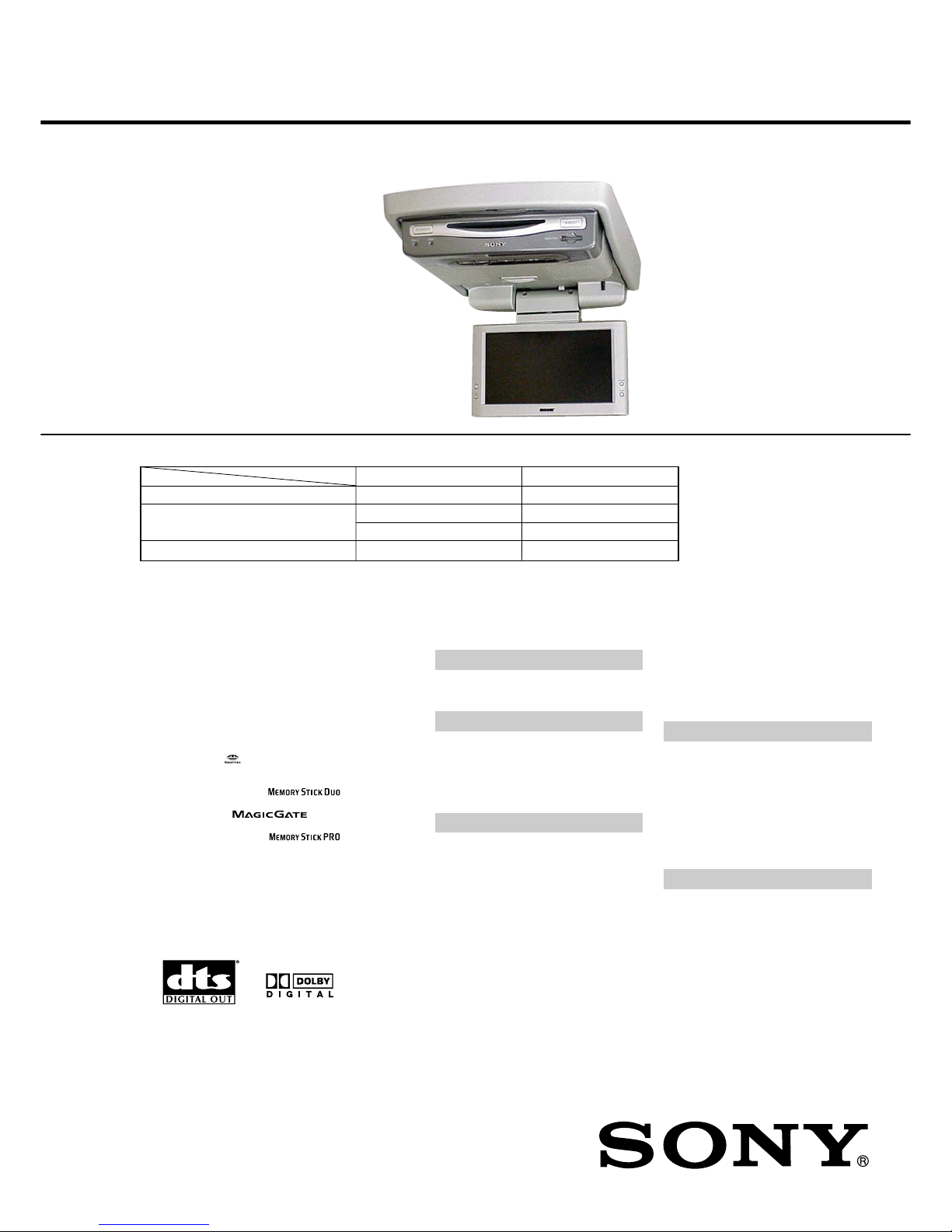
MOBILE DVD SYSTEM
US Model
MV-900SDS
Ver. 1.4 2006.08
9-877-871-05
2006H05-1
© 2006.08
Sony Corporation
eVehicle Division
Published by Sony Techno Create Corporation
SPECIFICATIONS
Copyrights
This product incorporates copyright protection
technology that is protected by method claims
of certain U.S. patents, other intellectual
property rights owned by Macrovision
Corporation, and other rights owners. Use of
this copyright protection technology must be
authorized by Macrovision Corporation, and is
intended for home and other limited viewing
uses only unless otherwise authorized by
Macrovision Corporation. Reverse engineering
or disassembly is prohibited.
• “Memory Stick,”
and “MagicGate
Memory Stick” are trademarks of Sony
Corporation.
• “Memory Stick Duo” and “
”
are trademarks of Sony Corporation.
• “MagicGate” and “ ” are
trademarks of Sony Corporation.
• “Memory Stick PRO” and “
”
are trademarks of Sony Corporation.
Manufactured under license from Dolby
Laboratories. “Dolby”, “Pro Logic”, and the
double-D symbol are trademarks of Dolby
Laboratories.
“DTS,” “DTS Digital Surround” and “DTS
Digital Out” are trademarks of Digital Theater
Systems, Inc.
DVD player XVM-R90D
System
Laser Semiconductor laser
Signal format system NTSC/PAL
Audio characteristics
Frequency response 20 Hz to 20 kHz
Signal to noise ratio 90 dB (A)
Harmonic distortion 0.05 %
Dynamic range 90 dB
Wow and flutter below measurable limits
(±0.001% W PEAK)
General
Outputs FM output
Audio output
Video output
Optical output
Inputs Audio input
Video input
DC 12V input
Power requirements 12 V DC
Dimensions Approx. 285 × 73 × 455 mm
(11
1
/4 × 2 7/8 × 18 in)
(w/h/d)
Mass Approx. 3.5 kg
(7 lb 12 oz)
Operating temperature 0 °C to 45 °C
(32 °F to 113 °F)
Supplied accessories Card remote commander
RM-X137
Power supply cord (1)
RF modulator cable (1)
Mounting plate (1)
Screws (5)
Tapping screws (8)
Operating Instructions (1)
Monitor
System Liquid crystal color display
Display Manual flipdown panel
Drive system TFT-LCD active matrix
system
Picture size 9 inches wide screen (16:9)
Picture segment 336,960 (w 1,440 × h 234)
dots
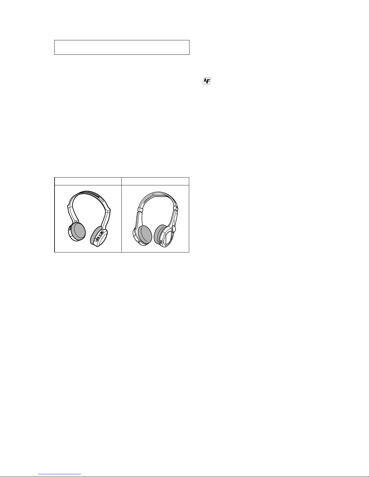
Cordless Stereo Headphones
MDR-IF0140
General
Modulation system Frequency modulation
Carrier frequency Right 2.8 MHz
Left 2.3 MHz
Frequency response 18 − 22,000 Hz
Power source DC 1.5 V (size AAA) dry
battery
Mass Approx. 125 g (4.41 oz)
including battery
Operating temperature 5 °C to 35 °C
(41 °F to 95 °F)
Design and specifications are subject to change
without notice.
MODEL NUMBER LABEL PRINTED MODEL NAME
DVD PLAYER MV-900SDS XVM-R90D
CORDLESS STEREO HEADPHONES
MDR-IF0140 MDR-IF0140
MV-01HP MV-01HP
CARD REMOTE COMMANDER – RM-X137
COMPONENT MODEL NAME
Note: There are two types of Cordless Stereo Headphones. For further information, see “NOTE WHEN
REPLACING THE CORDLESS STEREO HEADPHONES” (page 3) of the Servicing Notes.

MV-900SDS
2
TABLE OF CONTENTS
1. SERVICING NOTES ................................................ 3
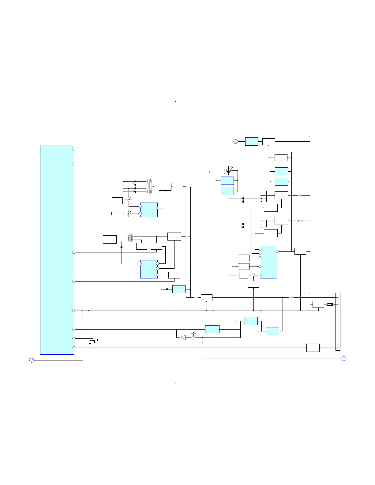
2. GENERAL
Location of Controls........................................................ 5
3. DISASSEMBLY
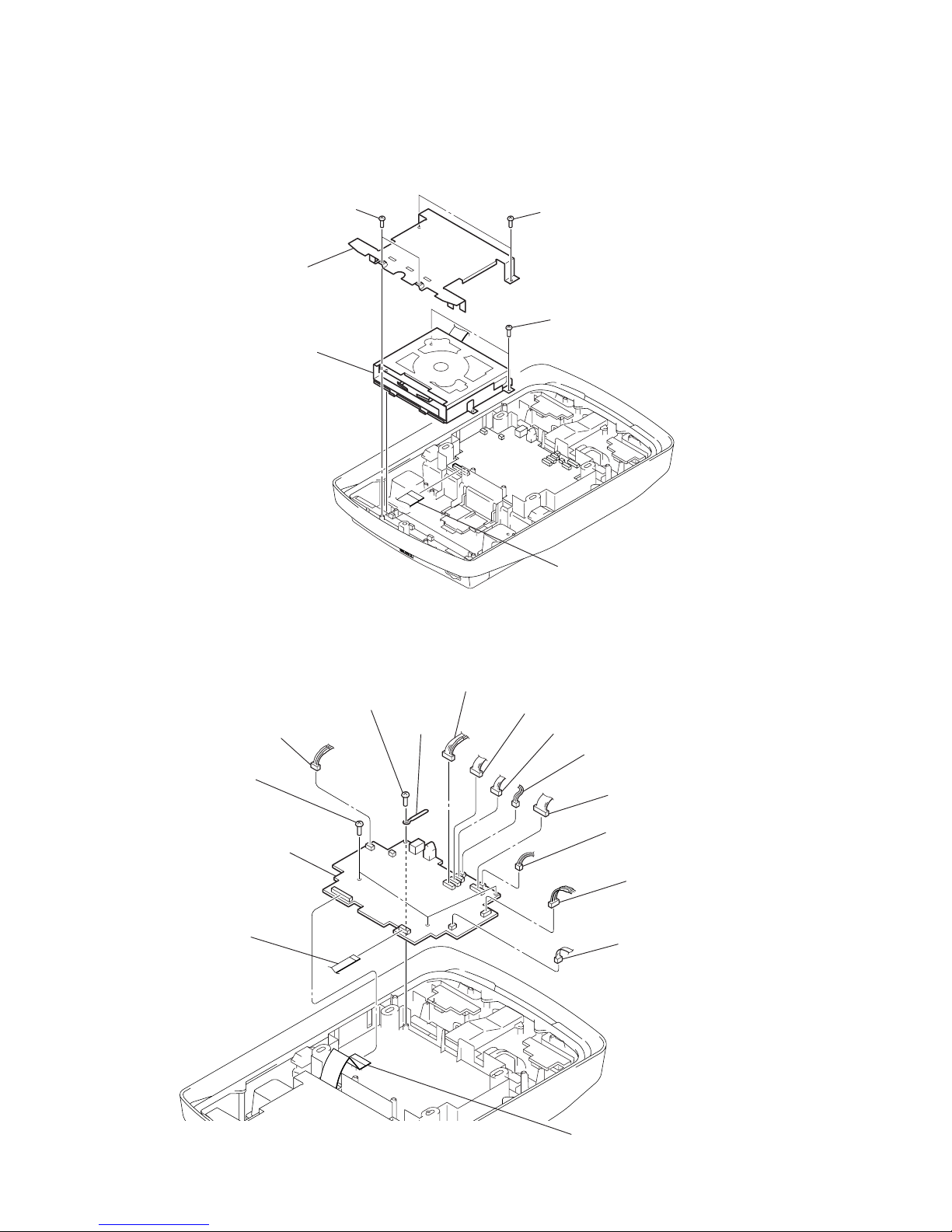
3-1. Disassembly Flow ........................................................... 9
3-2. Bracket (Main) ................................................................ 9
3-3. DVD Mechanism Deck Block ......................................... 10
3-4. MAIN Board.................................................................... 10
3-5. Rear Cover (Hinge) ......................................................... 11
3-6. LCD Block ...................................................................... 11
3-7. LCD Board ...................................................................... 12
3-8. Liquid Crystal Display Panel (LCD1) ............................. 12
4. TEST MODE.............................................................. 13
5. ELECTRICAL ADJUSTMENTS ......................... 14
6. DIAGRAMS
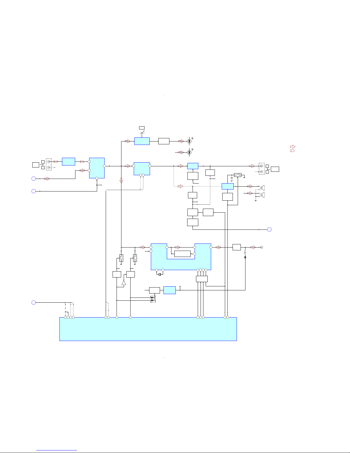
6-1. Block Diagram – MPEG DECODER Section – ............ 19
6-2. Block Diagram – AUDIO Section – ............................... 20
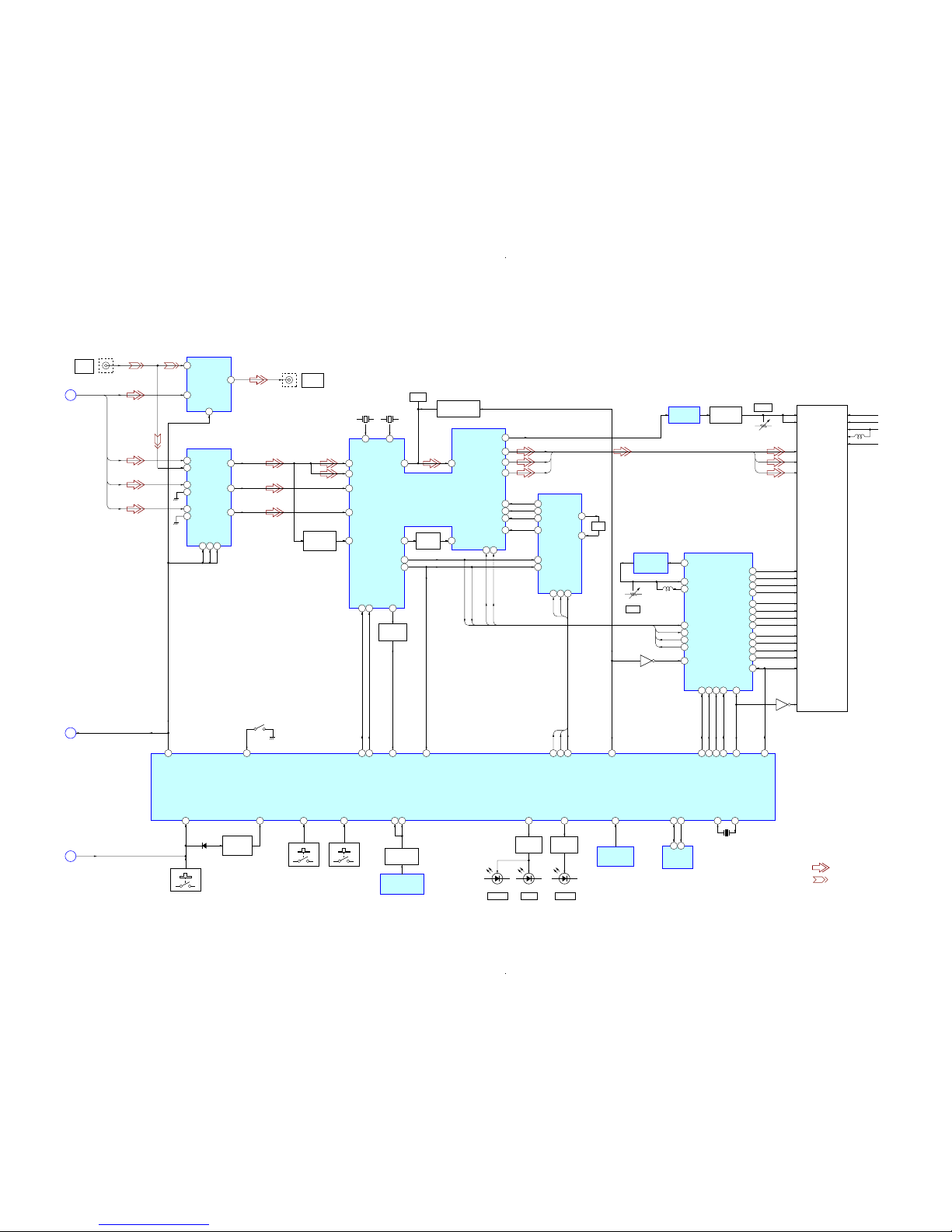
6-3. Block Diagram – VIDEO, PANEL Section –................. 21
6-4. Block Diagram – POWER SUPPLY Section – .............. 22
6-5. Printed Wiring Board
– MAIN Board (Component Side) – ............................... 24
6-6. Printed Wiring Board
– MAIN Board (Conductor Side) – ................................. 25
6-7. Schematic Diagram – MAIN Board (1/4) – ................... 26
6-8. Schematic Diagram – MAIN Board (2/4) – ................... 27
6-9. Schematic Diagram – MAIN Board (3/4) – ................... 28
6-10. Schematic Diagram – MAIN Board (4/4) – ................... 29
6-11. Printed Wiring Board – LCD Board (Side A) – ............. 30
6-12. Printed Wiring Board – LCD Board (Side B) – ............. 31
6-13. Schematic Diagram – LCD Board (1/4) – ...................... 32
6-14. Schematic Diagram – LCD Board (2/4) – ...................... 33
6-15. Schematic Diagram – LCD Board (3/4) – ...................... 34
6-16. Schematic Diagram – LCD Board (4/4) – ...................... 35
6-17. Printed Wiring Board – PANEL Section (1/2) – ............ 36
6-18. Printed Wiring Boards – PANEL Section (2/2) – ........... 37
6-19. Schematic Diagram – PANEL Section –........................ 38
7. EXPLODED VIEWS
7-1. Skirt (Cabinet) Section .................................................... 54
7-2. Front (Panel) Section ....................................................... 55
7-3. MAIN Board Section....................................................... 56
7-4. Cabinet (Base) Section .................................................... 57
7-5. LCD Section.................................................................... 58
8. ELECTRICAL PARTS LIST................................ 59
Notes on chip component replacement
• Never reuse a disconnected chip component.
• Notice that the minus side of a tantalum capacitor may be
damaged by heat.
Flexible Circuit Board Repairing
• Keep the temperature of the soldering iron around 270 ˚C
during repairing.
• Do not touch the soldering iron on the same conductor of the
circuit board (within 3 times).
• Be careful not to apply force on the conductor when soldering
or unsoldering.
CAUTION
Use of controls or adjustments or performance of procedures
other than those specified herein may result in hazardous radiation
exposure.
CAUTION
The use of optical instruments with this
product will increase eye hazard.
DANGER INVISIBLE LASERRADIATIONWHEN OPEN.
AVOID DIRECT EXPOSURE TO BEAM.
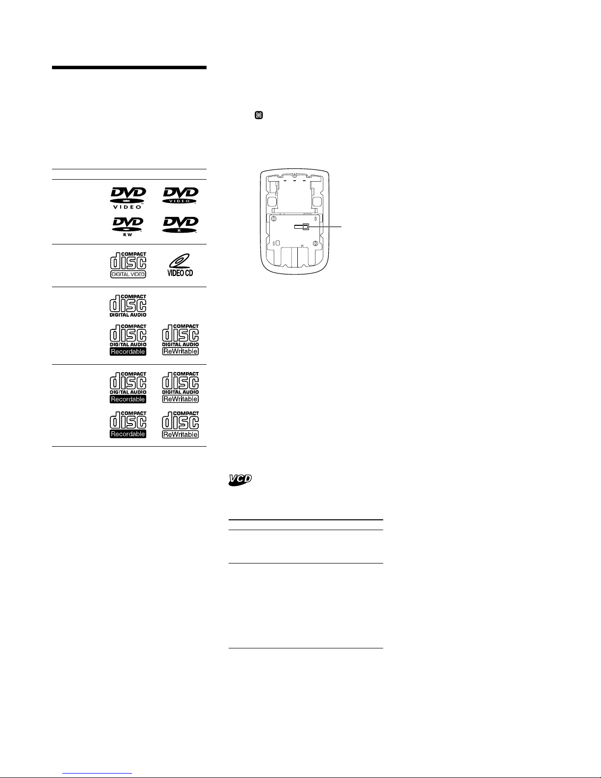
This is located on the drive unit's internal
chassis.
3
MV-900SDS
SECTION 1
SERVICING NOTES
The laser diode in the optical pick-up block may suffer electrostatic
break-down because of the potential difference generated by the
charged electrostatic load, etc. on clothing and the human body.
During repair, pay attention to electrostatic break-down and also
use the procedure in the printed matter which is included in the
repair parts.
The flexible board is easily damaged and should be handled with
care.
NOTES ON LASER DIODE EMISSION CHECK
Never look into the laser diode emission from right above when
checking it for adjustment. It is feared that you will lose your sight.
NOTE WHEN REPAIRING OR REPLACING THE
CORDLESS STEREO HEADPHONES
The Cordless Stereo Headphones attached to this set have been
changed in the midway of production.
Repair or replace the Cordless Stereo Headphones after making sure
which type they are by referring to the following figure.
NOTES ON HANDLING THE OPTICAL PICK-UP
BLOCK OR BASE UNIT
UNLEADED SOLDER
Boards requiring use of unleaded solder are printed with the leadfree mark (LF) indicating the solder contains no lead.
(Caution: Some printed circuit boards may not come printed with
the lead free mark due to their particular size)
: LEAD FREE MARK
Unleaded solder has the following characteristics.
• Unleaded solder melts at a temperature about 40 ˚C higher
than ordinary solder.
Ordinary soldering irons can be used but the iron tip has to be
applied to the solder joint for a slightly longer time.
Soldering irons using a temperature regulator should be set to
about 350 ˚C.
Caution: The printed pattern (copper foil) may peel away if
the heated tip is applied for too long, so be careful!
• Strong viscosity
Unleaded solder is more viscou-s (sticky, less prone to flow)
than ordinary solder so use caution not to let solder bridges
occur such as on IC pins, etc.
• Usable with ordinary solder
It is best to use only unleaded solder but unleaded solder may
also be added to ordinary solder.
O
P
E
N
O
N
O
F
F
P
OW
E
R
VOL
ON
OFF
VOL
MDR-IF0140 MV-01HP
Ver. 1.4
4
MV-900SDS
About discs this player can
play
This player can play the following discs:
• DVD
• DVD-R/DVD-RW
• Video CD
• Audio CD
• CD-R/CD-RW
Disc type Label on the disc
“DVD VIDEO,” “DVD-R” and “DVD-RW” are
trademarks.
DVD VIDEOs
Video CDs
Audio CDs
MP3 files/
JPEG files
Notes on CD-Rs (recordable CDs)/
CD-RWs (rewritable CDs)/DVD-Rs
(recordable DVDs)/DVD-RWs
(rewritable DVDs)
• Some CD-Rs/CD-RWs/DVD-Rs/DVD-RWs
(depending on the equipment used for its
recording or the condition of the disc) may
not play on this player.
• You cannot play a CD-R/CD-RW/DVD-R/
DVD-RW that is not finalized*.
• You cannot play a CD-R/CD-RW that is
recorded in Multi Session.
• You can play MP3/JPEG files recorded on
CD-ROMs, CD-Rs, and CD-RWs.
* A process necessary for a recorded CD-R/CD-RW
disc to be played on the audio CD player.
Region code of DVDs this player
can play
This player has a region code printed on the
rear of the player and will only play DVDs that
are labeled with identical region codes. DVDs
labeled
ALL
will also be played on this player.
If you try to play any other DVD, the message
“REGION ERROR” will appear on the screen.
Depending on the DVD, the region code
indication may not appear even if the DVD is
prohibited by area restrictions.
Region
code
Cautions
• This player CANNOT play these discs.
— DVD-Audio — DVD-RAM
— DVD-ROM — CD-G
— SVCD — CD-I
— Photo-CD — VSD
— Active-Audio (Data)
— CD-Extra (Data)
— Mixed CD (Data)
— CD-ROM (the data other than the MP3/JPEG
file)
— DVD-RW recorded in VR mode
• This product incorporates copyright protection
technology that is protected by method claims of
certain U.S. patents and other intellectual
property rights owned by Macrovision
Corporation and other rights owners. Use of this
copyright protection technology must be
authorized by Macrovision Corporation, and is
intended for home and other limited viewing
uses only unless otherwise authorized by
Macrovision Corporation. Reverse engineering or
disassembly is prohibited.
Note on PBC (Playback Control)
This player conforms to Ver. 1.1 and Ver. 2.0 of
Video CD standards. You can enjoy two kinds
of playback according to the disc type.
Disc type
Video CDs without
PBC functions
(Ver. 1.1 discs)
Video CDs with
PBC functions
(Ver. 2.0 discs)
You can
Video playback (moving
pictures) as well as music.
• Interactive software
with menu screens
displayed on the
monitor.
•Video playback
functions.
• High-resolution still
pictures if they are
included on the disc.
5
MV-900SDS
SECTION 2
GENERAL
This section is extracted from
instruction manual.
9
0
qa
qs
qd
qf
qg
qh
1
2
3
4
5
6
7
8
Refer to the pages listed for details.
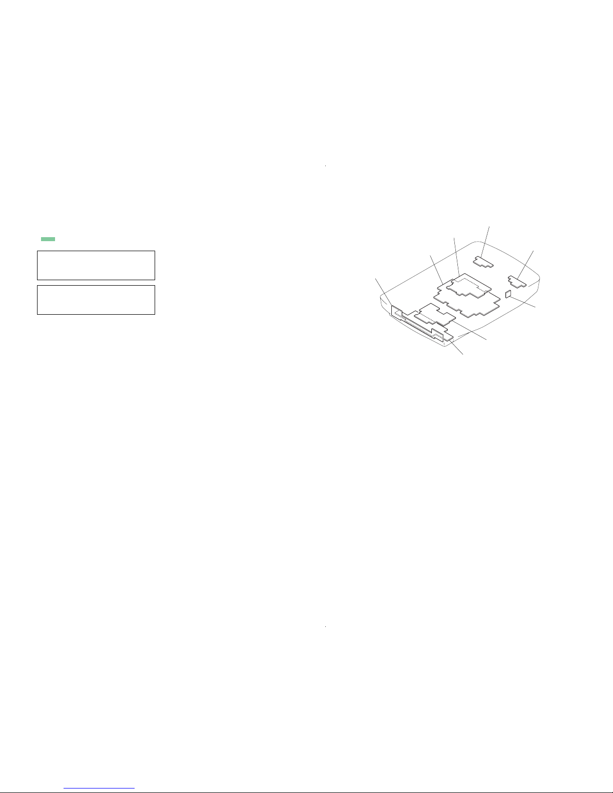
1 Disc slot
2 POWER (on/off) button
To turn on/off the player.
3 DISC IN light
When a disc is in the player, the DISC IN
light glows orange.
4 RESET button
5 . (previous)/> (next) buttons
6 Receptor for the card remote
commander/Transmitter for the cordless
headphones
7 Monitor
8 VOL +/– buttons
To turn up or down the volume or to select
the item during menu operation.
9 EJECT button
Available to eject a disc from the player
even when the player is turned off.
q; “Memory Stick” slot
qa x (stop) button
qs u (play/pause) button
qd OPEN button
Slide to open the monitor.
qf Speakers (left/right)
qg REVERSE button
To switch images upside down and
reverse the output of the audio channels.
qh MENU button
To make various display settings and FM
transmitter setting.
Note
Even when the player is turned off by pressing
(POWER), you can eject a disc from the player,
though you cannot insert a disc.
Location of controls
XVM-R90D
6
MV-900SDS
ENTER
SEARCH
POWER
DISPLAY
CLEAR
SETUP
AUDIO
ANGLE
SUBTITLE
MENU
TOP MENU
INPUT
123
456
7 890
VOL
Refer to the pages listed for details.
1 DISPLAY button
To display the time information of the disc.
2 Number buttons (0 to 9)
3 TOP MENU button
To display the top menu of a recorded
DVD.
4 MENU button
To display the recorded DVD menu, or to
turn on/off the PBC (Playback control)
menu of a Video CD.
5 O (return) button
6 ./> (previous/next) buttons
7 m (fast reverse)/
M (fast forward) buttons
8 M/,/m/< buttons
9 POWER (on/off) button
To turn on/off the player.
q; SEARCH button
To specify a desired point on a disc by
chapter, title, or track.
qa CLEAR button
qs SUBTITLE button
To change the subtitle language while
playing a DVD.
qd ENTER button
To enter a setting.
qf ANGLE button
To select the multiple angles of view while
playing a DVD.
qg AUDIO button
To change the audio output/audio
language.
qh
(slow reverse)/y (slow forward)
buttons
qj u (play/pause) button
qk x (stop) button
ql SETUP button
Used to perform menu operations.
w; INPUT button
To select the input source.
wa VOL (–/+) buttons
To turn up or down the volume.
The corresponding buttons of the card
remote commander control the same
functions as those on the player.
Instructions in this manual describe how to use
the player by mainly using the card remote
commander.
Tip
Refer to “Replacing the lithium battery” for details
on how to replace the battery.
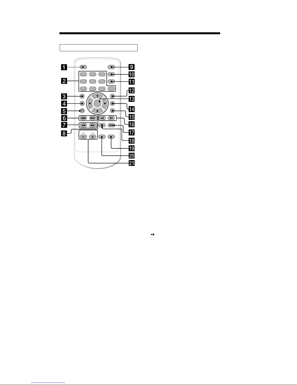
Card remote commander RM-X137
7
MV-900SDS
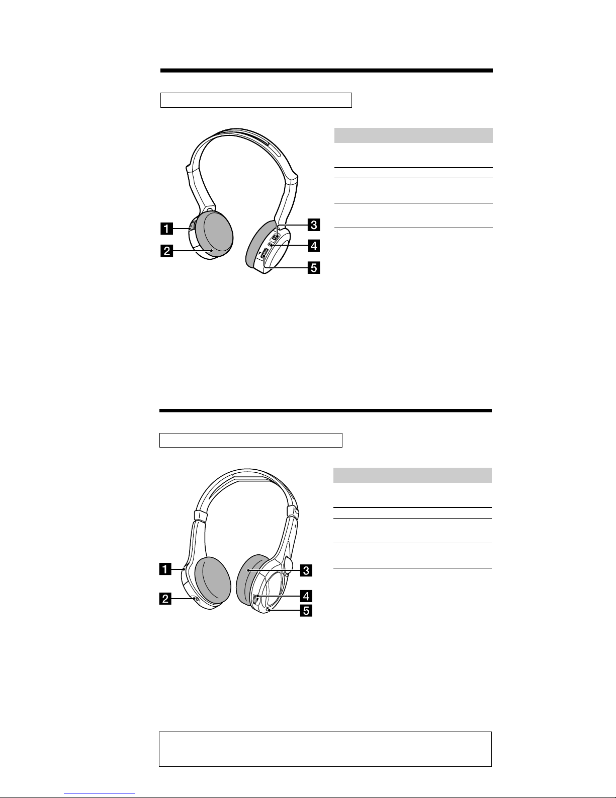
Cordless Stereo Headphones MDR-IF0140
1 Battery compartment lid
To set a battery, open the lid.
2 Ear pad
The ear pads are replaceable.
3 Power (ON/OFF) switch
4 POWER indicator
When the power switch of the headphones
is set to ON, the POWER indicator lights
up in red.
5 VOL control dial
To adjust the volume level from 0 to 10.
O
P
EN
ON
O
F
F
POW
ER
VO
L
Battery life
Size AAA dry battery (1) is supplied with the
headphones.
Battery Approx. hours*
1
Sony alkaline battery 60 hours*
2
LR03/AM-4 (N)
Sony manganese battery 28 hours*
2
R03/UM-4 (NU)
*1at 1 kHz, 1 mW+1 mW output
*
2
Time stated above may vary, depending on the
temperature or conditions of use.
Tip
Refer to “Replacing the battery” for details on
how to replace the battery.
Ver. 1.4
Cordless Stereo Headphones MV-01HP
1 Battery compartment lid
To set a battery, open the lid.
2 Power (ON/OFF) switch
3 Ear pad
4 VOL control dial
To adjust the volume level from 0 to 10.
5 POWER indicator
When the power switch of the headphones
is set to ON, the POWER indicator lights
up in red.
ON
OF
F
VO
L
Battery life
Size AAA dry battery (2) is supplied with the
headphones.
Battery Approx. hours*
1
Sony alkaline battery 60 hours*
2
LR03/AM-4 (N)
Sony manganese battery 28 hours*
2
R03/UM-4 (NU)
*1at 1 kHz, 1 mW+1 mW output
*
2
Time stated above may vary, depending on the
temperature or conditions of use.
Tip
Refer to “Replacing the battery” for details on
how to replace the battery.
Note: There are two types of Cordless Stereo Headphones. For further information, see “NOTE
WHEN REPLACING THE CORDLESS STEREO HEADPHONES” (page 3) of the Servicing
Notes.
8
MV-900SDS
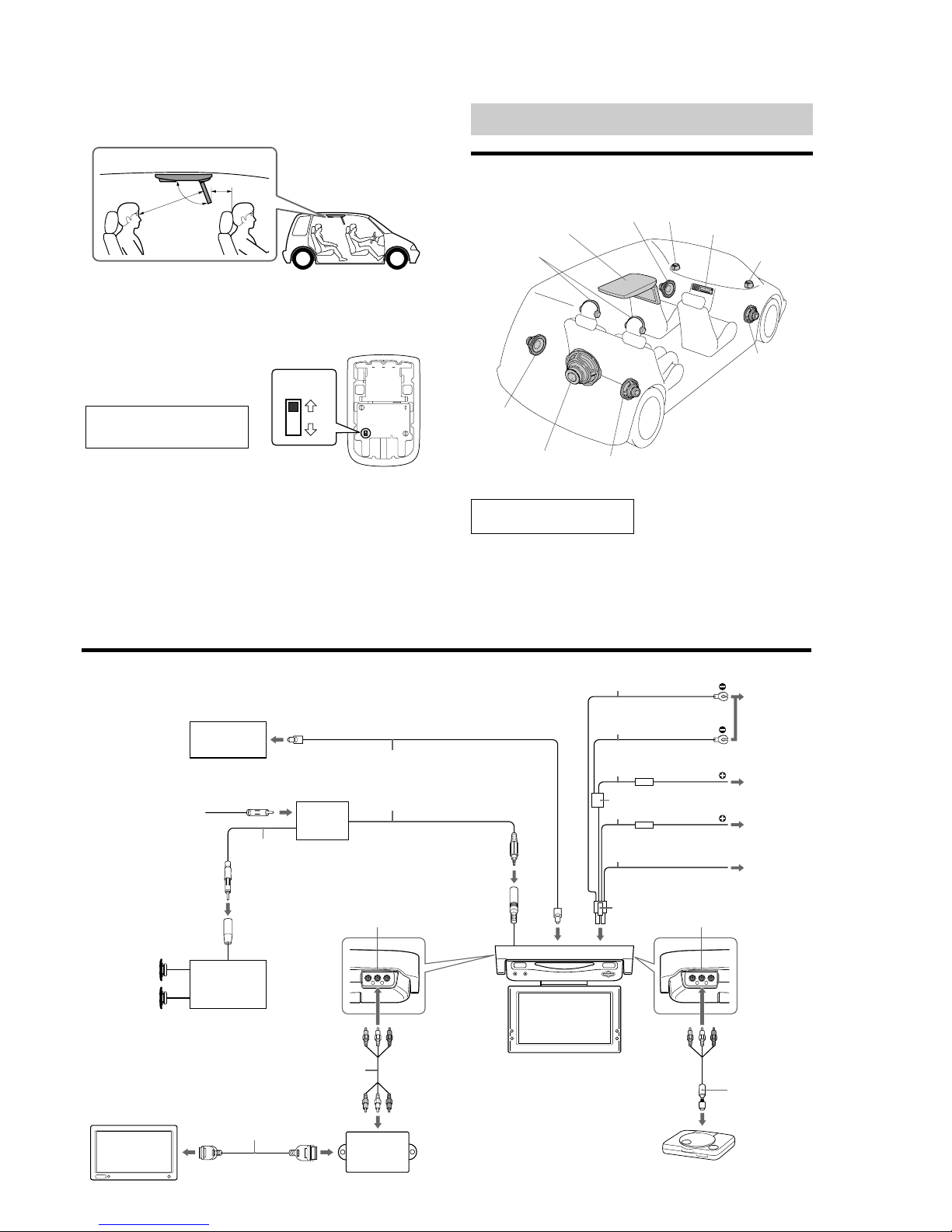
Where to install
Before installing this unit, please check your local traffic rules and regulations. Follow the diagram
below to install this unit in a suitable position in your car.
Do not install this unit where:
— It will obstruct the driver’s view when the
monitor is in either the open or closed
position.
— It will obstruct the operation of the airbag
system.
— It will obstruct the operation of the
vehicle, especially the steering wheel, shift
lever, or brake pedal.
—A driver or passengers may injure
themselves when getting into or out of the
car.
If you have any questions or problems
concerning your unit that are not covered
in this manual, please consult your
nearest Sony dealer.
Before installing
Make sure that the POWER SELECT switch is
set to the correct position.
A*: If your car has an accessory position on
the ignition key.
B : If your car has no accessory position on
the ignition key.
* A is the factory preset position.
When the POWER SELECT switch is
set to B
Press (POWER) on the player to turn on.
The player does not turn on by pressing
(POWER) on the card remote commander.
Note
Be sure to turn off the player after driving your
car.
To turn off the player, follow the operations
below:
– Press (POWER) on the player.
– Press (POWER) on the card remote commander.
If the power is left on, it will cause battery drain.
B
A
POWER SELECT
switch
Connections
Installation diagram
Refer to the installation diagram and ask a qualified technician for the installation of the unit.
DVD player
XVM-R90D
Front Left
speaker
Rear Left
speaker
Subwoofer
Tweeter Left
Head unit
Front Right
speaker
Rear Right
speaker
Cordless Stereo
Headphones
MDR-IF0140
Be sure to securely fasten all equipment to
the car chassis, etc., to prevent them
moving while your car is in motion.
Note
All equipment other than one DVD player and two
cordless stereo headphones is optional.
Notes on the locations for PS one™
Do not set PS one™:
— on a dashboard, or in a place subject to direct
sunlight.
— in a place near magnetic source such as
magnets, speakers and a TV/Monitor.
— on an unstable or uneven surface.
— in a place subject to excessive vibration.
— in a place subject to excessive dust or dirt.
— in poorly ventilated or humid place.
— in a place to subject to temperature extremes
(below 5˚C (41˚F) or above 35˚C (95˚F)).
Refer to the operating instructions supplied to PS
one™.
“PS one” is a trademark of Sony Computer
Entertainment Inc.
Tweeter Right
Connection diagram
Refer to the connection diagram for the proper connections.
Note
Set the POWER SELECT switch before installing (page 6).
Optical cable
(optional)
AUDIO/VIDEO OUTPUT
Connection box
(optional)
From the car antenna
RCA pin cord (optional)
Car audio
(optional)
Antenna connector*
1
Speaker system
(optional)
*
1
An adapter (optional) may be necessary for your
car and car audio system. In such a case, consult
your dealer.
*
2
If your car has no ACC (accessory) position on
the ignition key switch, set the POWER SELECT
switch to B (page 6) and connect this ACC cable
to the +12 V power (battery) terminal.
Monitor cable (optional)
Monitor (optional)
Relay box
5 m
Amplifier equipped
with a digital input
(optional)
0.5 m
GND (1 m)
Back-up (5 m)
To a metal surface
of the car chassis
To car battery
(12 V)
To ignition switch*
2
(ACC position)
4 Pin Power connector
PS one™ (optional)
ACC (5 m)
Fuse (5 A)
Fuse (1 A)
Red
Yellow
Black
Precautions on PS one™
• Be sure to fasten PS one™ in a safe place
securely.
• For your safety, do not use PS one™ while
driving your car.
• Make sure that the operating voltage of PS
one™ is 7.5 V. Other voltages may cause
malfunction, or damage PS one™.
Refer to the operating instructions supplied to
PS one™.
“PS one” is a trademark of Sony Computer
Entertainment Inc.
GND (1 m)
POWER REM (5 m)
Blue
Max. supply current 0.3 A
To a power
amplifier
Black
Filter box
AV Cable
(integrated audio/video)
(optional)
AUDIO/VIDEO INPUT
MV-900SDS
9
• This set can be disassembled in the order shown below.
3-1. DISASSEMBLY FLOW
3-2. BRACKET (MAIN)
(Page 9)
3-3. DVD MECHANISM
DECK BLOCK
(Page 10)
3-4. MAIN BOARD
(Page 10)
3-5. REAR COVER (HINGE)
(Page 11)
3-6. LCD BLOCK
(Page 11)
3-7. LCD BOARD
(Page 12)
3-8. LIQUID CRYSTAL
DISPLAY PANEL
(LCD1)
(Page 12)
SET
SECTION 3
DISASSEMBLY
4
six screws
(BTP2.6
×
8)
2
two screws
(BTP2.6
×
8)
1
four screws
(B2.6
×
4)
5
bracket (main
)
3
bracket (support)
Note: Follow the disassembly procedure in the numerical order given.
3-2. BRACKET (MAIN)
MV-900SDS
10
3-4. MAIN BOARD
3
screw
(BTP2.6
×
8)
4
harness
2
connector (CN108)
2
connector (CN105)
2
connector (CN107)
2
connector (CN302)
2
connector (CN103)
2
connector (CN104)
2
connector (CN701)
2
connector (CN705)
1
flexible flat cable
(50P) (CN101)
1
flexible flat cable
(30P) (CN102)
5
MAIN board
2
connector (CN702)
3
three screws
(BTP2.6
×
8)
2
two screws
(BTP2.6
×
6)
4
bracket (front)
3
two screws
(BTP2.6
×
8)
1
flexible flat cable
(50P) (CN101)
5
two screws
(BTP2.6
×
8)
6
DVD mechanism
deck block
3-3. DVD MECHANISM DECK BLOCK
MV-900SDS
11
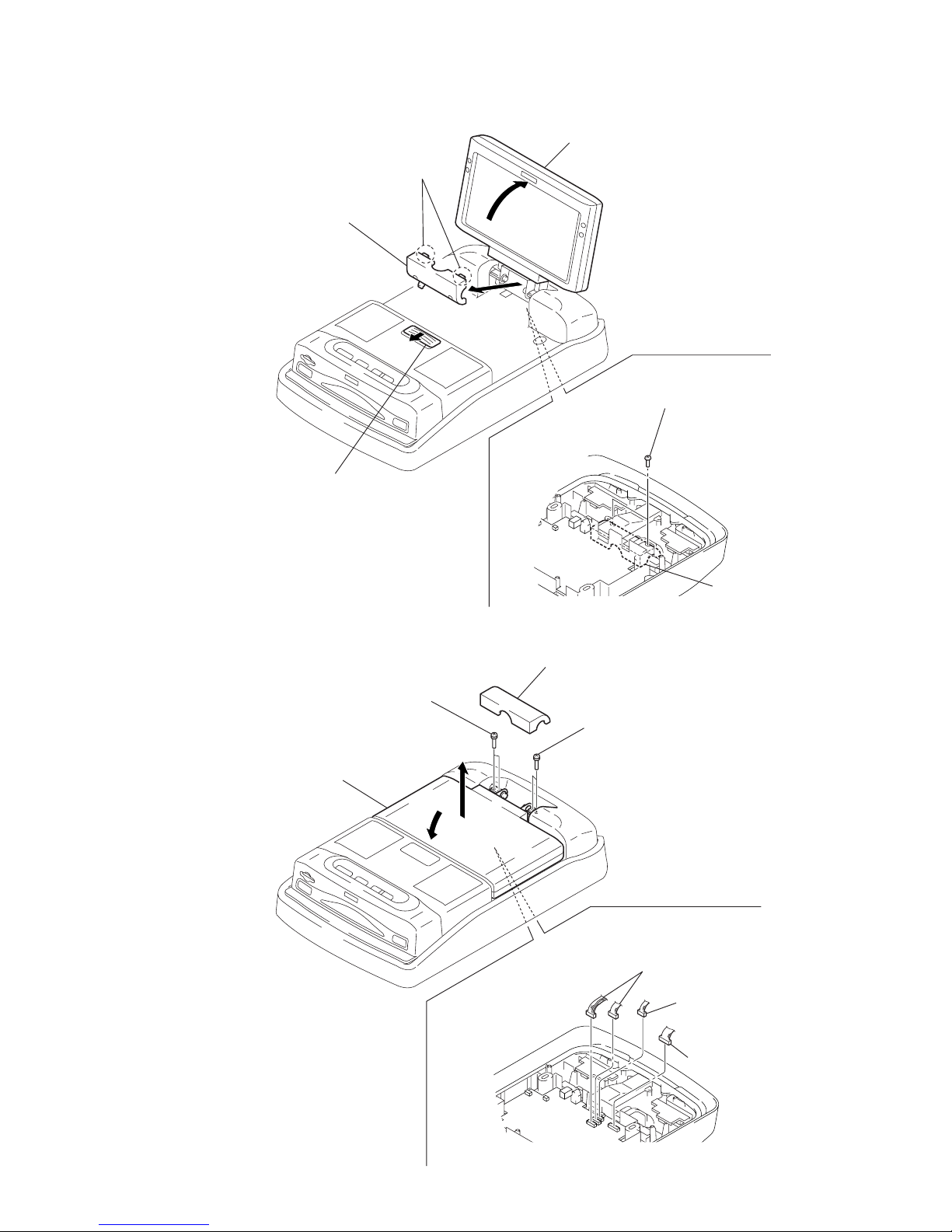
3-5. REAR COVER (HINGE)
3-6. LCD BLOCK
4
rear cover
(hinge)
1
Slide the knob (open) in the direction
of arrow A, and open the LCD block
in the direction of arrow B.
A
LCD block
B
3
two claws
2
two screws
(P2 × 8)
rear cover
(hinge)
3
front cover (hinge)
5
Lifting up the LCD block in
the direction of arrow
A
.
2
two connectors
(CN105, 108)
1
A
2
connector
(CN107)
2
connector
(CN103)
4
two screws
(PS3
×
10)
4
two screws
(PS3
×
10)
MV-900SDS
12
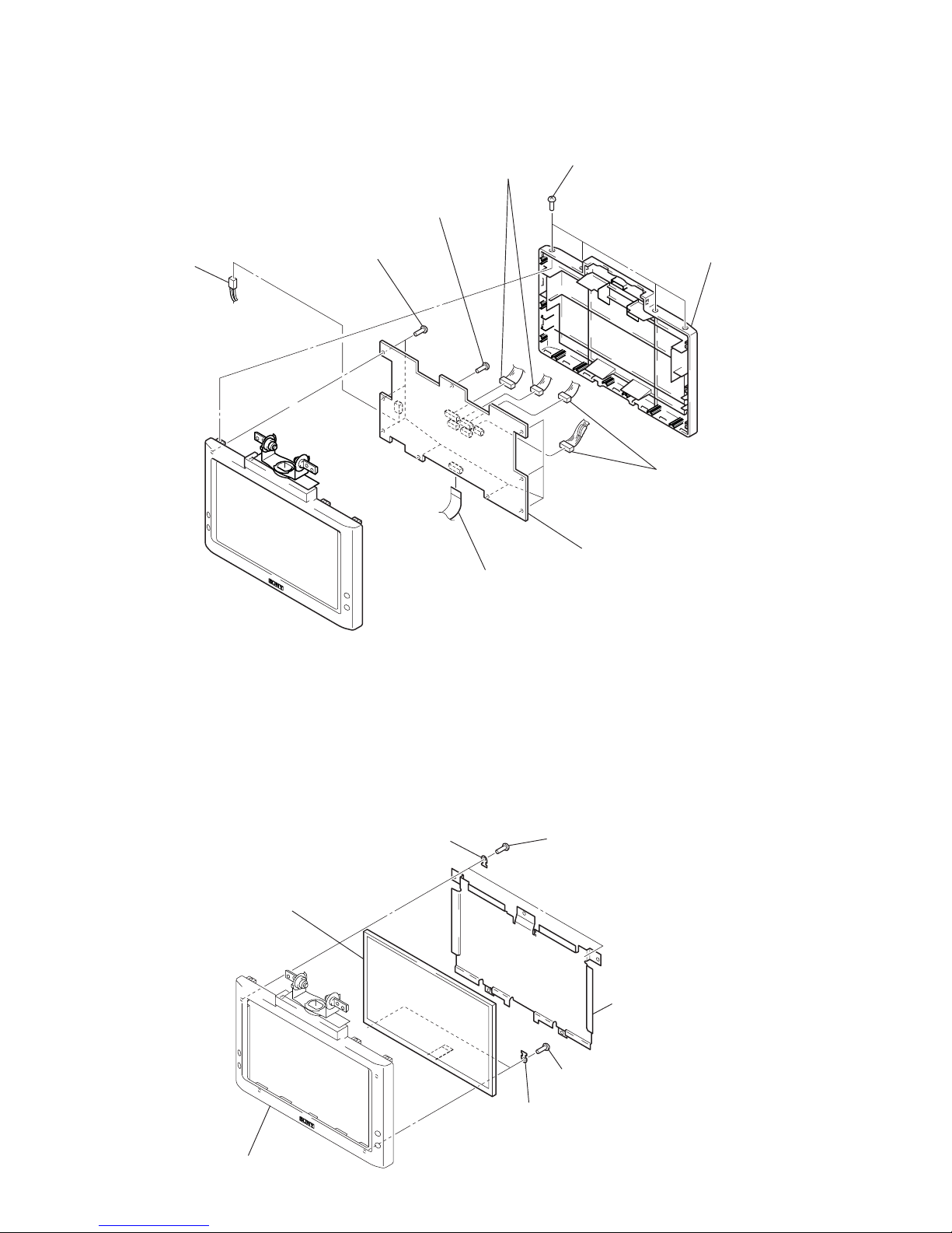
3-7. LCD BOARD
3-8. LIQUID CRYSTAL DISPLAY PANEL (LCD1)
5
eight screws
(BTP2 × 6)
6
screw
(PS2.6 × 6)
4
two connectors
(CN906, 907)
1
four screws
(B2 × 5)
2
rear case (LCD
)
4
two connectors
(CN905, 908)
7
LCD board
3
flexible board
(CN801)
4
connector
(CN850)
1
two screws
(BTP2 × 6)
4
two screws
(BTP2 × 6)
5
two retainers
(LCD)
2
two retainers (LCD)
6
liquid crystal display panel
(LCD1)
front case (LCD) block
3
shield plate
(LCD)

13
MV-900SDS
SECTION 4
TEST MODE
Note: This set is able to setting the adjustment data, reset to factory default
and initialize the EEPROM (IC402 on the MONITOR board) in the
test mode.
ENTER THE TEST MODE
Procedure:
1. Press the [POWER] button to turn the power ON.
2. While pressing the [VOL --] and . buttons, press the
[RESET] button.
3. The set is enter the test mode and display as bellow figure.
Note: If initial data is not written to the EEPROM (IC402 on the MONITOR
board) or data is clobbered, the set is not able to display normally
screen.
BATCH WRITING OF THE INITIAL DATA TO
EEPROM
In the test mode, by pressing the [VOL --] button at two seconds,
batch writing is possible of the initial data to EEPOM (IC402 on
the MONITOR board).
OPERATION OF THE TEST MODE
All operations are performed using the bellow buttons.
RELEASING THE TEST MODE
In the test mode menu screen, press the [MENU] button to select “8.
SOFT RESET (EXIT)”, and press the [REVERSE] button to release
the test mode.
OPERATING THE EACH ITEM
1. NTSC/PAL SELECT
In this mode, switch the signal format system to NTSC or P AL.
2. FOR FACTORY
In this mode, change the data of adjustment data.
Enter this mode, it displays each adjustment item as follow.
1) Com Gain
2) Y Gain
3) Black Limit
4) White Limit
5) R-Sub BRT
6) B-Sub BRT
7) R-Sub CONT
8) B-Sub CONT
9) Gamma 1
10) Gamma 2
11) VCO Free Run
12) PLL/V Pos
13) H Pos
3. LCD SETTING
This mode is not used in servicing.
4. FM TRANSMITTER
In this mode, switch the frequency range of FM transmitter as
follow.
1) USA (88.3 to 89.9 MHz)
2) Japan (76.5 to 79.5 MHz)
3) Transmitter off
5. HEAT PROTECTION
This mode is not used in servicing.
6. VOLTAGE SETUP
This mode is not used in servicing.
7. LOAD DEFAULT
This mode is not used in servicing.
8. SOFT RESET (EXIT)
Releasing the test mode.
Display
TEST MODE MENU
1. NTSC/PAL SELECT
2. FOR FACTORY
3. LCD SETTING
4. FM TRANSMITTER
5. HEAT PROTECTION
6. VOLTAGE SETUP
7. LOAD DEFAULT
8. SOFT RESET(EXIT)
Dream System 20XX
Ver.20XX-XX-XXx
Button Function
MENU Select the item
REVERSE Enter
VOL + Up the data value
VOL − Down the data value
14
MV-900SDS
1. DC/DC CONVERTER ADJUSTMENT
1-1. Frequency Adjustment
Setting:
Procedure:
1. Connect an oscilloscope or frequency counter to the TP802
and TP804 on the MONITOR board.
2. Check that the voltage between TP951 (−) and TP952 (+) is
14.4 V. Press the [POWER] button to turn the power on.
3. Adjust the RV801 on the MONITOR board so that the value
of oscilloscope or frequency counter becomes 243 kHz ±3
kHz.
1-2. 5V Voltage Adjustment
Setting:
Procedure:
1. Connect a digital voltmeter to the TP804 and TP807 on the
MONITOR board.
2. Check that the voltage between TP951 (–) and TP952 (+) is
14.4 V. Press the [POWER] button to turn the power on.
3. Adjust the RV803 on the MONITOR board so that the value
of digital voltmeter becomes 5.05 V ±0.03 V.
1-3. Other Voltages Check
Setting:
Procedure:
– Vdd Voltage Check –
1. Connect a digital voltmeter to the TP804 and TP808 on the
MONITOR board.
2. Check that the voltage between TP951 (–) and TP952 (+) is
14.4 V. Press the [POWER] button to turn the power on.
3. Check that the value of digital voltmeter is 3.45 V ±0.2 V.
– Vgh Voltage Check –
4. Connect the digital voltmeter to the TP804 and TP806 on the
MONITOR board.
5. Check that the value of digital voltmeter is 17.5 V ±1.5 V.
– Vss Voltage Check –
6. Connect the digital voltmeter to the TP804 and TP805 on the
MONITOR board.
7. Check that the value of digital voltmeter is –12.0 V ±1.5 V.
2. PLL ADJUSTMENT
Setting:
Procedure:
1. Connect a digital voltmeter to the TP601 and TP602 on the
MONITOR board.
2. Check that the voltage between TP951 (–) and TP952 (+) is
14.4 V. Press the [POWER] button to turn the power on.
3. Adjust the RV601 on the MONITOR board so that the value
of digital voltmeter becomes 2.4 V ±0.15 V.
3. INVERTER HIGH VOLTAGE CHECK
Setting:
Procedure:
– High Voltage Check –
1. Connect a digital voltmeter (for withstand high voltage) to the
TP853 and TP854 on the MONITOR board.
2. Check that the voltage between TP951 (–) and TP952 (+) is
14.4 V. Press the [POWER] button to turn the power on.
(DIMMER: off)
3. Check that the value of digital voltmeter is 550 V ±150 V
(rms).
– Frequency Check –
4. Connect an oscilloscope (use a probe for withstand high
voltage) to the TP853 and TP854 on the MONITOR board.
5. Check that the frequency of oscilloscope is 66 kHz ±2.5 kHz.
4. OSD DOT CLOCK CHECK
Setting:
Procedure:
1. Connect a frequency counter (high impedance) to the TP403
and TP405 on the MONITOR board.
2. Check that the voltage between TP951 (–) and TP952 (+) is
14.4 V. Press the [POWER] button to turn the power on.
3. Check that the value of frequency counter is 6.5 MHz ±0.2
MHz.
+
–
oscilloscope
or
frequency counte
r
MONITOR board
TP802
TP804
+
–
digital voltmete
r
MONITOR board
TP807
TP804
+
–
digital voltmete
r
MONITOR board
TP805/TP806/TP808
TP804
+
–
digital voltmete
r
MONITOR board
TP601
TP602
+
–
digital voltmete
r
MONITOR board
TP853
TP854
+
–
frequency counte
r
MONITOR board
TP403
TP405
SECTION 5
ELECTRICAL ADJUSTMENTS
15
MV-900SDS
5. NTSC SUB CARRIER CHECK
Setting:
Procedure:
1. Connect a frequency counter (high impedance) to the TP510
and TP513 on the MONITOR board.
2. Check that the voltage between TP951 (–) and TP952 (+) is
14.4 V. Press the [POWER] button to turn the power on.
3. In the normal mode, press the [INPUT] key on the remote
commander to select the “VIDEO” mode.
4. Input NTSC video signal to the “VIDEO INPUT” jack (J701
on the VIDEO (IN) board).
5. Check that the value of frequency counter is 3.579545 MHz
±100 Hz.
6. PAL SUB CARRIER CHECK
Setting:
Procedure:
1. Connect a frequency counter (high impedance) to the TP510
and TP513 on the MONITOR board.
2. Check that the voltage between TP951 (–) and TP952 (+) is
14.4 V. Press the [POWER] button to turn the power on.
3. In the normal mode, press the [INPUT] key on the remote
commander to select the “VIDEO” mode.
4. Input PAL video signal to the “VIDEO INPUT” jack (J701 on
the VIDEO (IN) board).
5. Check that the value of frequency counter is 4.433619 MHz
±100 Hz.
7. V-COM ADJUSTMENT
Setting:
Procedure:
– Voltage Set-up Adjustment –
1. Connect an oscilloscope to the TP819 and TP832 on the
MONITOR board.
2. Check that the voltage between TP951 (–) and TP952 (+) is
14.4 V. Press the [POWER] button to turn the power on.
3. Enter the test mode, and enter the “2. FOR FA CTOR Y” mode.
(refer to “4. TEST MODE”)
4. Press the [MENU] button to display “Com Gain”, and press
the [REVERSE] button.
5. Adjust by pressing the [+]/ – buttons so that the voltage of
oscilloscope becomes 6.3 Vp-p ±0.1 V.
6. Press the [REVERSE] button and write the date to EEPROM
(IC402 on the MONITOR board).
– Waveform Position Set-up Adjustment –
7. Adjust the RV802 on the MONITOR board so that A value
of waveform becomes –1.7 V ±0.1 V.
8. VIDEO ADJUSTMENT
Note: Perform the following adjustment items in test mode.
Common Setting:
1. Check that the voltage between TP951 (–) and TP952 (+) is
14.4 V. Press the [POWER] button to turn the power on.
2. Enter the test mode, and enter the “2. FOR FA CTOR Y” mode.
(refer to “4. TEST MODE”)
3. Set the signal format system to NTSC. (refer to “4. TEST
MODE”)
4. Input 10 steps signal (NTSC, without burst) to the VIDEO
INPUT jack (J301 on the POWER board) from pattern
generator.
Waveform of input signal
fig. 8-1
Waveform of output signal
(TP810, TP811, TP812)
fig. 8-2
1 Contrast Level of Luminance Signal
Setting:
Procedure:
1. Connect an oscilloscope to the TP513 and TP811 on the
MONITOR board.
2. Press the [MENU] button to display “Y Gain”, and press the
[REVERSE] button.
3. Adjust by pressing the [+]/ – buttons so that the D value of
waveform (fig. 8-2) becomes 3.4 V V.
4. Press the [REVERSE] button and write the date to EEPROM
(IC402 on the MONITOR board).
+
–
frequency counte
r
MONITOR board
TP510
TP513
+
–
frequency counte
r
MONITOR board
TP510
TP513
+
–
oscilloscop
e
MONITOR board
TP819
TP832
6.3 Vp-p ± 0.1
V
4.6 V ± 0.1 V
A
: – 1.7 V ± 0.1
V
0 V
0.286 V
1 Vp-p
0 V
AB CDE
+
–
oscilloscop
e
MONITOR board
TP811
TP513
+0.2
–0.1
16
MV-900SDS
2 Back Limiter Level
Procedure:
1. In the “1 Contrast Level of Luminance Signal” status, press
the [MENU] utton to display “Black Limit”, and press the
[REVERSE] button.
2. Adjust by pressing the [+]/ – buttons so that the A value of
waveform (fig. 8-2) becomes 1.0 V V.
3. Press the [REVERSE] button and write the date to EEPROM
(IC402 on the MONITOR board).
3 White Limiter Level
Procedure:
1. In the “2 Black Limiter Level” status, press the [MENU] button
to display “White Limit”, and press the [REVERSE] button.
2. Adjust by pressing the [+]/ – buttons so that the E value of
waveform (fig. 8-2) becomes 3.9 V V.
3. Press the [REVERSE] button and write the date to EEPROM
(IC402 on the MONITOR board).
4 R-sub Bright
Procedure:
1. In the “3 White Limiter Level” status, connect the
oscilloscope to the TP513 and TP810 on the MONITOR board.
2. Press the [MENU] button to display “R-Sub BRT”, and press
the [REVERSE] button.
3. Adjust by pressing the [+]/ – buttons so that the A value of
waveform (fig. 8-2) becomes 1.0 V V.
4. Press the [REVERSE] button and write the date to EEPROM
(IC402 on the MONITOR board).
5 B-sub Bright
Procedure:
1. In the “4 R-sub Bright” status, connect the oscilloscope to
the TP513 and TP812 on the MONITOR board.
2. Press the [MENU] button to display “B-Sub BRT”, and press
the [REVERSE] button.
3. Adjust by pressing the [+]/ – buttons so that the A value of
waveform (fig. 8-2) becomes 1.0 V V.
4. Press the [REVERSE] button and write the date to EEPROM
(IC402 on the MONITOR board).
6 R-ch Sub Contrast
Procedure:
1. In the “5 B-sub Bright” status, connect the oscilloscope to
the TP513 and TP810 on the MONITOR board.
2. Press the [MENU] button to display “R-Sub CONT”, and press
the [REVERSE] button.
3. Adjust by pressing the [+]/ – buttons so that the D value of
waveform (fig. 8-2) becomes 3.4 V V.
4. Press the [REVERSE] button and write the date to EEPROM
(IC402 on the MONITOR board).
7 B-ch Sub Contrast
Procedure:
1. In the “6 R-ch Sub Contrast” status, connect the oscilloscope
to the TP513 and TP812 on the MONITOR board.
2. Press the [MENU] button to display “B-Sub CONT”, and press
the [REVERSE] button.
3. Adjust by pressing the [+]/ – buttons so that the D value of
waveform (fig. 8-2) becomes 3.4 V V.
4. Press the [REVERSE] button and write the date to EEPROM
(IC402 on the MONITOR board).
8 Gamma 1
Procedure:
1. In the “7 B-ch Sub Contrast” status, connect the oscilloscope
to the TP513 and TP811 on the MONITOR board.
2. Press the [MENU] button to display “Gamma 1”, and press the
[REVERSE] button.
3. Adjust by pressing the [+]/ – buttons so that the B value of
waveform (fig. 8-2) becomes 1.9 V V.
4. Press the [REVERSE] button and write the date to EEPROM
(IC402 on the MONITOR board).
9 Gamma 2
Procedure:
1. In the “8 Gamma 1” status, press the [MENU] button to display
“Gamma 2”, and press the [REVERSE] button.
2. Adjust by pressing the [+]/ – buttons so that the C value of
waveform (fig. 8-2) becomes 3.1 V V.
3. Press the [REVERSE] button and write the date to EEPROM
(IC402 on the MONITOR board).
q; VCO Free Run
Setting:
Procedure:
1. In the “9 Gamma 2” status, connect a frequency counter to
the TP506 and TP513 on the MONITOR board.
2. Press the [MENU] button to display “VCO Free Run”, and press
the [REVERSE] button.
3. Adjust by pressing the [+]/ – buttons so that the value of
frequency counter becomes 15.734 kHz ±50 Hz.
4. Confirm that the displayed screen is normally display.
5. Press the [REVERSE] button and write the date to EEPROM
(IC402 on the MONITOR board).
qa Vertical Position
Procedure:
1. In the “q; VCO Free Run” sta tus, input the monoscope signal
to the VIDEO INPUT jack (J301 on the POWER board).
2. Press the [MENU] button to display “PLL/V Pos”, and press
the [REVERSE] button.
3. Adjust by pressing the [+]/ – buttons so that the vertical position
of screen on the monitor becomes the most suitable.
4. Press the [REVERSE] button and write the date to EEPROM
(IC402 on the MONITOR board).
qs Horizontal Position
Procedure:
1. In the “qa Vertical Position” status, press the [MENU] button
to display “H Pos”, and press the [REVERSE] button.
2. Adjust by pressing the [+]/ – buttons so that the horizontal
position of screen on the monitor becomes the most suitable.
3. Press the [REVERSE] button and write the date to EEPROM
(IC402 on the MONITOR board).
+
–
frequency counte
r
MONITOR board
TP506
TP513
+0.2
–0.1
+0.2
–0.1
+0.2
–0.1
+0.2
–0.1
+0.2
–0.1
+0.2
–0.1
+0.2
–0.1
+0.2
–0.1
17
MV-900SDS
Adjustment Location:
– LCD BOARD (Side A) –
RV601
RV802
RV803
RV801
TP853
TP983
– LCD BOARD (Side B) –
TP854
TP506
TP952 (+)
TP951 (
−
)
TP513
TP805
TP807
TP804
TP802
TP811
TP828
TP812
TP810
TP601
TP602
TP510
TP405
TP987
TP832
TP808
TP819
TP806
TP403

18
MV-900SDS
MEMO
MV-900SDS
1919
MV-900SDS
DA-BE
CK-BE
CS-BE
DA-BE
CK-BE
CS-BE
LOW-PASS
FILTER
IC701
: DVD (VIDEO)
: DIGITAL OUT
: DVD (AUDIO)
: CHECK OUT
: CHECK IN
145
• SIGNAL PATH
• R-ch is omitted due to same as L-ch.
+8V
HD0 – HD15
+5V
B+8V
B+5V
DVD MECHANISM
DECK BLOCK
198
XLWRLL
RST
XHRST
HDO – HD15
144
HINTJ
HIRQ
155
HA1
HA1
154
HA0
HA0
158
HA2
HA2
146
IORDY
HIORDY
149
IOWJ
XHWR
150
IORJ
XHRD
152
HCS1J
XHCS1FX
151
HCS16J
XHIOCS16
153
HCS3J
HCS3FX
166
ENDSW
ENDSW
2 DATA
16 SCK
1 BCK
R-CH
L-CH_AU
3 LRCK
15 ML
14 MC
13 MD
MPEG DECODER
IC1
EEPROM
IC5
D/A CONVERTER
IC7
114VBS
113Y
108B-Y
106R-Y
CVBS
CVBS,
Y, B-Y, R-Y
Y
B-Y
R-Y
33DAC DATA
41SPDIF
OPTICAL
TRANSCEIVER
J301
FLASH ROM
IC3
DQ0 - DQ14
A–1, A0 - A18
RESET SIGNAL
GENERATOR
IC2
7VOUTL
R-CH
8VOUTR
24XRESET
12XRST
11ZEROR
39DAC MCLK
40DAC BCK
32DAC LRCK
165DAC ML
143DAC MC
118DAC MD
122 – 128,
131 – 137, 140, 141
MUTING
Q702, 704
DELAY
D13, Q3
MUTING
SWITCH
Q1, 2
OPTICAL
OUTPUT
142 MS SDIO
117 MC SCLK
167 MS BS
119 MS INS
B+3.6V
MS SDIO
MC SCLK
MS BS
MS INS
VCC
VCC
MEMORY
STICK
178 - 182, 185 - 191,
194 - 196
77 - 82, 85 - 90,
93 - 96
204 - 207, 2-7,
10 - 16, 19 - 21
45, 25, 24 - 16,
8 - 1, 48
29 - 36, 38 - 44
176
XLCS3
170
XLOE
28
XOE
26
XCE
11
XWE
74
DBANK173DBANK0
SD-RAM
IC6
DQ0 - DQ15 A0 - A11
DB0 - DB15 DMA0 - DMA11 LD0 - LD14 LA0 - LA19
B+5V
2, 4, 5, 7, 8, 10, 11, 13, 42,
44, 45, 47, 48, 50, 51, 53
53 - 58,
61 - 66
22 - 26,
29 - 25, 22
69
XDCAS72XDRAS0
18
XRAS0
17
XCAS
20
BA021BA1
71
XDWE
100
XDCS0
70
DSCK_EN
102
DSCK
38
CLK37CKE
19
XCS
16
XWE
101
DQM
168169162
39
DQMH
160
SDA
5
SDA
161
SCL
4
SCL
A
B
DA-BE, CK-BE,
CS-BE
C
SECTION 6
DIAGRAMS
6-1. BLOCK DIAGRAM – MPEG DECODER Section –
(Page 21)
(Page 20)
(Page 20)
MV-900SDS
2020
MV-900SDS
6-2. BLOCK DIAGRAM – AUDIO Section –
(Page 19)
(Page 22)
(Page 19)
• SIGNAL PATH
: DVD (AUDIO)
: AUX INPUT (AUDIO)
• R-ch is omitted due to same as L-ch.
IR TRANSMITTER
MODULATOR
IC904
AUDIO INPUT
SELECT
IC704
BPF
FL201
MUTING
Q708
LOW-PASS FILTER
Q208, 209
BUFFER
Q205
BUFFER
Q206
LEVEL SHIFT
Q210 – 213
STANDBY
SWITCH
Q710, 711
DISCHARGE SWITCH
Q714, 715
MUTING
SWITCH
Q318
MUTING
CONTROL
Q316, 317
DIFFERENTIAL
AMP
IC703
R-CH
J701 (1/2)
R
AUDIO
INPUT
L
R-CH
R-CH
FM+5V
R-CH
D317
D204
Q204
Q207
Q202
Q202, 204
RF LEVEL
SWITCHING
J702 (1/2)
R
POWER ON
L
FM STEREO
MODULATOR
IC201
R-CH
5
MPX ADJ
11
RF OUT
17
DATA16CLK15CE18ATT
9
VTIN
7
PD
22
LIN
64
AMP ON
15
DA (IN)-BE
49
FM150FM2
4
FM-DATA
3
FM-CLK
7
S-SDA
6
S-SCL
5
FM-CE
POWER ON
MUTING
Q319, 320
16
DA (OUT)-BE
17
CK-BE18CS-BE
DA-BE
CK-BE
CS-BE
1
RIN
POWER AMP
IC707
LED DRIVE
Q902
LINE AMP
IC708
MUTING
Q713
XOUT
XIN
14 13
X201
7.6MHz
SYSTEM CONTROLLER
IC401 (1/3)
R-CH
SP1
(L)
SP2
(R)
R-CH
R-CH
(FM MODULATOR)
B+8V
POWER ON
MUTING
Q321, 322
53
AMUTE
E
AUDIO
OUTPUT
R-CH
L-CH_AU
B
DA-BE, CK-BE,
CS-BE
C
SW1
D
RV900
VCO
8
5
7
ELECTRICAL VOLUME
IC706
D912, 914, 916
(IR TRANSMITTER)
LIN1
CLK4DATA
CLK
DATA
CLK
DATA
LOUT1
1
7
VIN1
3 VIN2
2
SW1
VOUT
D911, 913, 915
(IR TRANSMITTER)
R-CH
B+8V
+5V
REGULATOR
IC304
B+ SWITCH
Q323, 324
+
(Page 21)
MV-900SDS
2121
MV-900SDS
PHASE
COMPARATOR
IC602
WAKE UP
SWITCH
Q401, 403
REMOTE CONTROL
RECEIVER
IC902
TEMPERATURE
SENSOR
IC901
16
1
7
OSD DRIVER
IC405
RGB DECODER
IC501
VR
17 VG
15 BLK
20 HSYNCN
SCLK2CSN3DATA
OSC OUT
8OSC IN
18 VB
53
CTRAPOUT
26
R-OUT
21
G-OUT
19
B-OUT
R
G
B
14
R-IN2
15
G-IN2
16
B-IN2
17
YS
18
BLAK36POL
BLAK
POL
HD
VD
DATA
CLK
CS
54
CTRAPIN
34
CSYNCOUT
32
HDOUT
31
VDOUT
28
VCOMOUT
35
VDIN
52
YIN
19 YSYNCN
33
12
20
LCD CONTROLLER
IC601
PD
36 VCO1
2HSYNCIN
5VDBIN
LTBOX4QHSEL31JUST13UD
3
CPHSEL
57
ZOOM
59
SIDE1
61
JUST
55
LR
58
SIDE2
6
SCL
5
SDA
STV1
26STV2
23STH1
24STH2
54
U/D
21
SYNC-DET
51
V-SCK
43
VD
52
V-SDA
63
SW1
23
N/P
29CPH1
27CPH2
25CPH3
16CPV
19OEV1
18OEV2
17OEV3
21OEH
28L/R
STV1
STV2
STH1
STH2
CPH1
CPH2
CPH3
CPV
OEV1
OEV2
OEV3
OEH
L/R
U/D
VCOM
VCOM
VHG
VDD1
VCC
VB
VEE
VGH +17V
LIQUID CRYSTAL
DISPLAY MODULE
LCD1
VDD +3.3V
VCC +5V
VSS –13V
8 BLACK
14 POL
37 VCO0
46 NP
57
CIN
5
B-Y IN
4
R-Y IN
46
CSYNCIN
V COM AMP
IC802
V COM BIAS
Q803 – 807
BUFFER
Q501
SYNC LOCK
Q505, 506
PAL/NTSC SWITCH
Q504
V-SDA48V-SCK47HSYNCLOCK
39
VXO-NTSC63VXO-PAL
64
SIRCS BUFFER
Q901
LED DRIVE
Q953
EEPROM
IC402
30
MONITOR SW
BLAK
POL
HD
Q601
VD
R
G
B
RED
GREEN
BLUE
OSC
TRAP
20
OSD SCLK
22
OSD CSN
19
OSD DATA
DATA
CLK
CS
RV802
V-COM
RV601
PLL
SYNC
SEPARATOR
Q502, 503
X502
4.43MHz
X501
3.58MHz
Q603
SYSTEM CONTROLLER
IC401 (2/3)
CVBS, Y,
B-Y, R-Y
A
SW1
D
RESET
F
X2
X1
41 40
KEY IN
27
DISC_LED
12
X401
4.19MHz
S401 – 404
S902, 903
KEY DVD
28
KEY PW/EJ
29
S904 – 907
REM HALT45REM IN
47
TEMP
33
SDA13SCL
14
KEY HALT
44
D902
D402
S908
(PANEL CLOSE DETECT)
(ON: CLOSE)
DISC IN
LED DRIVE
Q955
LIGHT PW/EJ
11
D901D900
POWER EJECT
• SIGNAL PATH
: DVD (VIDEO)
: AUX INPUT (VIDEO)
J701 (2/2)
J702 (2/2)
VIDEO
INPUT
VIDEO
OUTPUT
12
VIDEO INPUT SELECT
IC102
VIDEO INPUT
SELECT
IC101
SW27SW3
1 IN1B
16 IN1A
9 IN3B
8 IN3A
14 IN2B
Y
CVBS
B-Y
R-Y
11 IN2A
2
SW1
1
SW1
3OUT1
6 VIN1
4 VIN2
2VOUT
6OUT3
5OUT2
6-3. BLOCK DIAGRAM – VIDEO, PANEL Section –
(Page 19)
(Page 20)
(Page 22)
MV-900SDS
2222
MV-900SDS
6-4. BLOCK DIAGRAM – POWER SUPPLY Section –
REGULATOR
CONTROL
Q302, 303
1
9
POWER CONTROL
IC301
B+5V
B+3.6V
E-VOL +8V
B+8V
D305
BATT
F301
D306
D307, 308
D315, 316
OUT1
10 OUT2
11 DT2
VCC
6 DT1
15 SCP
36
RESET
DEAD TIME
Q310
DEAD TIME
Q314
SWITCHING
Q312
LATCH
Q313
SWITCHING
REGULATOR
Q301
+8V
REGULATOR
IC303
+12V
REGULATOR
IC302
IR +8V
+8V
REGULATOR
IC903
VCC +7.5V
VCC
+8V
REGULATOR
IC950
U-COM +3.3V
+3.3V
REGULATOR
IC952
ACCESSORY
DETECT
Q315
RESET SIGNAL
GENERATOR
IC403
46
ACC IN
SWITCHING
REGULATOR
IC306
B+ SWITCH
Q309, 311
B+2.8V
SWITCHING
REGULATOR
IC305
PANEL +5V
+5V
REGULATOR
IC951
REGULATOR
CONTROL
Q305, 306
SWITCHING
REGULATOR
Q304
SWITCHING
REGULATOR
Q855, 856, 859
BACK LIGHT
UNIT
DC/DC
CONVERTER
Q801, 802
SW12V
B+ SWITCH
Q951, 952
B+ SWITCH
Q853, 854
OSC
Q857, 858
5V
VOLTAGE
(DC/DC CONVERTER)
(DC/DC CONVERTER)
DIMMER
Q860, 861
60
DIMMER
8
FAN CONT
48
IR CONT
56
TFT ON
2
PW-ON
31
ACC Y/N
B
A
S301
(POWER SELECT)
1
11
POWER CONTROL
IC850
D852, 853
D950
INVERTER
TRANSFORMER
T850
1IN+
C2
162IN+
12VCC
+
D801
S901
Q402
RESET
D802
D803
D804
VSS –13V
VGH +17V
VCC +5V
VDD +3.3V
3
POWER CONTROL
IC801
DC/DC
CONVERTER
T801
1IN+
71OUT
2RT
RV803
RV801
FREQUENCY
POWER ON
E
RESER
F
SYSTEM CONTROLLER
IC401 (3/3)
IR LED B+
M301
(FAN)
B+SWITCH
Q904, 905
B+SWITCH
Q307, 308
B+ SWITCH
Q325, 326
F950
3
CN301
2
4
BATT
AMP REM
ACC
F850
F801
D903
F951
F302
MM
DISC SLOT
ILLUMINATION
(Page 21)
(Page 20)
MV-900SDS
2323
MV-900SDS
• Note for Printed Wiring Boards and Schematic Diagrams • Circuit Boards Location
Note on Printed Wiring Boards:
• X : parts extracted from the component side.
• Y : parts extracted from the conductor side.
• x : parts mounted on the conductor side.
• : Pattern from the side which enables seeing.
(The other layers' patterns are not indicated.)
Caution:
Pattern face side: Parts on the pattern face side seen from
(Side B) the pattern face are indicated.
Parts face side: Parts on the parts face side seen from
(Side A) the parts face are indicated.
Caution:
Pattern face side: Parts on the pattern face side seen from
(Conductor Side) the pattern face are indicated.
Parts face side: Parts on the parts face side seen from
(Component Side) the parts face are indicated.
Note on Schematic Diagram:
• All capacitors are in µF unless otherwise noted. (p: pF)
50 WV or less are not indicated except for electrolytics
and tantalums.
• All resistors are in Ω and 1/
4
W or less unless otherwise
specified.
• C : panel designation.
• A : B+ Line.
• B : B– Line.
• H : adjustment for repair.
• Power voltage is dc 14.4V and fed with regulated dc power
supply from ACC and BATT cords.
• Voltages and waveforms are dc with respect to ground
under no-signal conditions.
no mark : DVD PLAY
(): STANDBY
∗ : Impossible to measure
• Voltages are taken with a V OM (Input impedance 10 MΩ).
Voltage variations may be noted due to normal production tolerances.
• Waveforms are taken with a oscilloscope.
Voltage variations may be noted due to normal production tolerances.
• Circled numbers refer to waveforms.
• Signal path.
L : DVD (VIDEO)
F : DVD (AUDIO)
J : DIGITAL OUT
a : AUX INPUT (VIDEO)
E : AUX INPUT (AUDIO)
d : CHECK IN
G : CHECK OUT
LCD board
FRONT board
KEY board
MAIN board
SERVO board
SW board
JACK (IN) board
JACK (OUT) board
MV-900SDS
2424
MV-900SDS
R784
R783
R735
R737
R734
R736
R754R755
R775
R769
R774
R768
R730
R731
R785
R782
R739
R741
R740
R738
R781
ECB
Q710
ECB
Q708
1
7
CN701
Q711
BCE
Q709
BCE
C759
+
C755
+
C745
+
C340
+
C757
+
C756
+
C727
+
C725
+
C724
+
C726
+
4
1
CN705
C734
+
C738
+
C732
+
C338
+
C736
+
C335
+
C397
+
C324
+
C735
+
C744
+
C743
+
C719
+
C718
+
R82
R86
CN102
R87
C383
R377
C82
C1 C2 C3
R5
R7
R8
R9
C135
C106
C105
C151
C24C25
C26
C27C28C29
C72
C30
R34
L4
C179
C178
C177
C134
C35
C34
C100
C32
R72
C99
C96
R21
R20
R19
R12
C4 C7 C18
R27
L56
C95
C44C52C58
C66
C68
R66
C71
C69
R42
C74
C78
C75
R68
R40
C104
C103
C102
C101
R43
R44
RB21
R85
R88
C149
R81
R80
R83
R84
Q3
BCEQ2BCE
ECB
Q1
AKA
D13
C150
+
CN101
C382
+
C386
+
C392
L314
+
C17
+
L313
C390
+
C395
+
R111R110R109
110
111
CN108
18
12
CN107
CN105
113
CN103
CN104
1
1
M301
(FAN)
2
2
CN302
D4
AK
RB2
RB1
RB3RB4RB5RB6RB7RB8
RB10
RB11
RB12
RB13
RB14
RB15
RB16
L304
L303
L306
L305
L302
L307
R236
R235
C219
C222
R218
R227
R228
R229
R230
C346 C345
R231R213
C221
R212
R215
R216
R214
R217
C218
R211
R1758
R1759
L704L705
R1760
R1761
R1762
C215
C328
+
1
61
3
CN201
CN702
L202
D204
KA
X201
IC304
IC1
IC101
Q208
SGD
ECB
Q209
Q205
BCE
Q207
BCE
Q206
BCE
C220
+
C344
+
C169
+
C342
+
C765
+
C766
+
C771
+
C772
+
C217
+
C211
+
C775
+
C776
+
C176
+
C162
+
C170
+
C175
+
C173
+
C22
+
C168
+
C161
+
C171
+
A
K
A
D317
C33
+
C144
+
C146
+
C381
+
C378
+
C370
+
C166
C255
+
R77
R73
R74
R75
R76
R712
R710
C704
R704
C703
R703
R711
R709
C710
+
C711
+
C702
+
C147
+
C705
+
C701
+
C706
+
C384
+
C372
+
C367
+
L3
L1
FB3
FB1
FB2
L101
L51
R106R104
C254
R103
R786
R108R107
R105
C343
+
C769
+
C226
+
C165
+
MAIN BOARD
(COMPONENT SIDE)
(11)
11
1-863-445-
52
53104
208157
1
105
156
JACK (IN)
BOARD
CN703
D
1
2
SP2
(R-CH)
3
4
SP1
(L-CH)
–
+
–
+
130
KEY BOARD
CN911
A
LCD BOARD
CN906
SW BOARD
B
LCD BOARD
CN907
G
LCD BOARD
CN905
H
LCD BOARD
CN908
F C
–
+
M
R70
136
4
150
11
FM
MODULATOR
ANTENNA
2
3
JACK (OUT)
CN704
E
A
B
C
D
E
F
G
H
I
1 2 3 4 5 6 7 8 9 10 11 12 13 14
J
13
L203
L701
L702
L703
C21
C19
L48
R25
R24
R29
R30
C23
R31
R32
C31
RB17
RB18
RB19
RB20
C365
+
C362
+
C364
+
SERVO BOARD
CN1
P
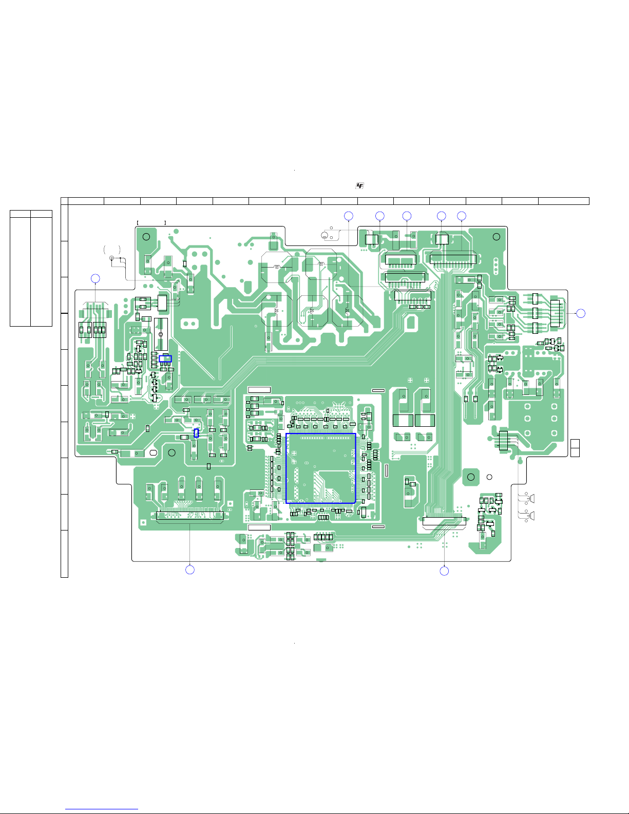
6-5. PRINTED WIRING BOARD – MAIN Board (Component Side) –
• See page 23 for Circuit Boards Location.
: Uses unleaded solder.
(Page 37)
(Page 30)
(Page 30) (Page 30)
(Page 37)
(Page 30)
(Page 37)
(Page 36)
• Semiconductor
Location
Ref. No. Location
D4 I-9
D13 I-12
D204 D-3
D317 F-3
IC1 H-7
IC101 G-4
IC304 E-3
Q1 I-12
Q2 I-12
Q3 I-12
Q205 E-3
Q206 F-3
Q207 E-3
Q208 D-2
Q209 E-3
Q708 E-12
Q709 E-12
Q710 D-14
Q711 D-14
Ver 1.1
(Supplement-1
page 11)
MV-900SDS
2525
MV-900SDS
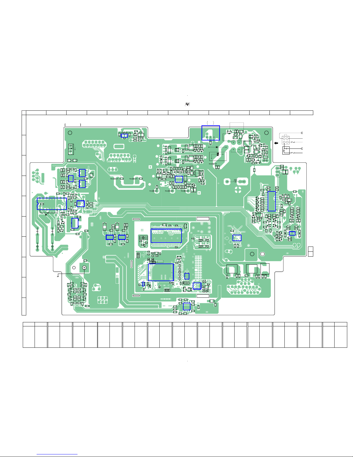
6-6. PRINTED WIRING BOARD – MAIN Board (Conductor Side) –
• See page 23 for Circuit Boards Location.
: Uses unleaded solder.
D203
AK
D201
D202
AK
D313
D312
D310
AK
D309
C225
R221
FL201
R220
C214
R223
R224
R225
R226
C231
C232
C224
C210
R203
C770
R787
R342R345
R205
R204
R365
R367
R364
C172
18
169
C174
C167
R366
C204
R202
C203
R201
R206
C209
R210
R1701
C773
R799
R1702
C774
R798
R794
R790
R793
IC708
IC102
IC201
R791
1
1
11
22
12
485
C216
C252
C227
C228
C229
C223
C212
C201
C202
C768R788
C767R789
R343
R207
R208
R344
C213
C230
R232
R209
R219
R795
R797
R796
R792
KA
L201
ECB
Q712
ECB
ECB ECB
ECB
Q203
Q204
Q202
Q324
Q323
Q201
ECB
Q210
ECB
Q211
ECB
Q212
ECB
Q213
Q322
Q321
Q713
BCE
BCE BCE
L308
L309
L311
C366
C368
C371
C373
C376
C379
C385
C377
C369
BCE
Q320
Q319
Q325
Q326
Q317
Q318
BCE
BCE
BCE
BCE
ECB
Q316
R361
R358
R340
R354
R360
R385 R384
R386
R359R362
R356
R353
R355
R351
C303
C302
C325
C307
C306
C305 C316
R313R314R306
R312R308
R322
R321
C350
C333R329C348
C310
C326
C351
C327 R318
C347
R317
R319
R315
R316
R324
R333
R334
R325
R305
R303
R304
R380
R302
R352
KA
R357
R339
ECB
TH301
KA
L312
L54
R78
C90C91
C10
R2R3R4
R1
R11
R16
L55
R22
L11
L12
L41
C14
C15
C9
R10
C6
R14
R17
R23
C8
C5
C94
C98C79
C157
R69
R71
R33
R54
R52
C84
C86
R62
R61
C87
C89
C143
R39
R57
L10
L9L8L7
R49
C80
C83
R47
R46
R90
R48
C145
C148
L706
C792
C794
L707
C793
16
IC7
9
18
4
IC5
IC3
IC2
1
48
25
1
24
58
8
IC701
5
14
8
IC306
IC305
IC303
5
14
4
IC706
IC707
IC705
IC703
1
18
16
9
58
4 1
5 8
4
158
IC704
4
158
8 5
14
L50
L2
D316
D315
D308
KA
KA
D307
KA
KA
D305
D306
AK
AK
ECB
ECBECB
Q310
Q311
BCE
R381
C332
R326 C330
C321C313
R331R332
R327
R328R323
C331
R378R379
R320
C349
Q309
Q303
ECB
Q314
Q302
C318
C317
R310
R311
R309
ECBECB
Q306
Q305
C329
F301 F302
R301
R307
Q304
Q301
Q313
Q312
D314
AK
D302
AK
R330
BCEBCE
814
171
IC301
IC302
C92
127
5428
IC6
A
K
D14
RB25
RB24
RB23
RB22
A
K
D12
L53
R708
R706
R707
R714
R716
R705
R727
R715
R713
C707
C708
C709
L52
X1
Q308
R337
R338R335
C337
C336
R336
Q307
BCE
C394
R370
C393
C389C388
C400
C387
C396
R371
R368
C391
R369
R372
D321D320
KA
KA
R1734
C790
R1710
C791
R1709
(CHASSIS)
C716
R726
R725
R723 R724
C795
C717
C714
R722
R721
C715
C712C713
R720
R719
R1733
Q703
BCE
ECB
Q704
Q701
BCE
ECB
Q702
R761
C796
C797
C253
R770
R766
R771
R777R779
R762
R763
R767
C758
R753
R747
R749
R752
C737
R748
R746
C748
R1766
C747
C749
C731 C730
C733
C751
C752
C746
C750
R772 R773
C721
R743
C723
R745
C720
R742
C722
R744
R751 R750
R764R765
R776
R1765
R1768
R1767
R1769
D701
R778
C341
L350
D304KAD303
AK
KAK
D318
A
K
D1
CN301
J301
D301
C301
VDR301
+
L301
C363
C315
+
C304
+
C309
+
C320
+
C314
+
C762
+
C764
+
C761
+
C763
+
MAIN BOARD
(CONDUCTOR SIDE)
(11)
11
1-863-445-
S301
(POWER SELECT)
A
B
1
D
DD
DGS
2
3 4
BLK
BLU
RED
BLK
YEL
GND
AMP REM
ACC
GND
BATT
+
F303
F304
TO
CN301
3
1
1
13
OPTICAL
OUTPUT
2
34
D
D
DDG
S
D
D
DDG
S
C
E
B
453
1
B
13
E
C
A
B
C
D
E
F
G
H
I
1 2 3 4 5 6 7 8 9 10 11 12 13 14
J
C97
AK
ECB
Q315
C339
R341
C398
R383
C251
2
1
3
Q715
BCE
Q714
BCE
Ref. No. LocationRef. No. Location
D1 F-8
D12 I-8
D14 H-8
D201 E-14
D202 C-13
D203 C-13
D301 B-10
• Semiconductor Location
Ref. No. Location Ref. No. Location Ref. No. Location
D302 C-8
D303 C-3
D304 C-3
D305 D-7
D306 D-7
D307 C-9
D308 C-9
D309 A-11
D310 B-11
D312 B-12
D313 C-12
D314 B-8
D315 D-9
D316 D-9
D318 C-12
D320 F-4
D321 F-5
D701 E-1
IC2 I-6
IC3 H-7
IC5 H-8
IC6 F-7
IC7 I-9
IC102 G-11
IC201 E-13
IC301 D-8
IC302 B-5
Ref. No. Location Ref. No. Location Ref. No. Location
IC303 F-3
IC305 F-4
IC306 F-6
IC701 J-9
IC703 D-3
IC704 C-3
IC705 D-3
IC706 E-3
IC707 E-2
IC708 F-14
J301 A-10
Q201 F-13
Ref. No. Location Ref. No. Location
Q202 F-13
Q203 F-13
Q204 F-13
Q210 E-12
Q211 E-12
Q212 E-12
Q213 E-12
Q301 C-8
Q302 C-9
Q303 C-9
Q304 B-8
Q305 B-9
Q306 B-9
Q307 A-6
Ref. No. Location
Q308 A-6
Q309 C-9
Q310 D-9
Q311 D-9
Q312 D-7
Q313 C-7
Q314 C-8
Ref. No. Location Ref. No. Location
Q315 A-11
Q316 C-12
Q317 C-12
Q318 C-11
Q319 B-12
Q320 B-12
Q321 F-13
Q322 G-13
Q323 E-12
Q324 E-12
Q325 B-12
Q326 B-12
Q701 J-3
Q702 J-3
Q703 I-3
Q704 I-3
Q712 F-14
Q713 F-14
MV-900SDS
2626
MV-900SDS
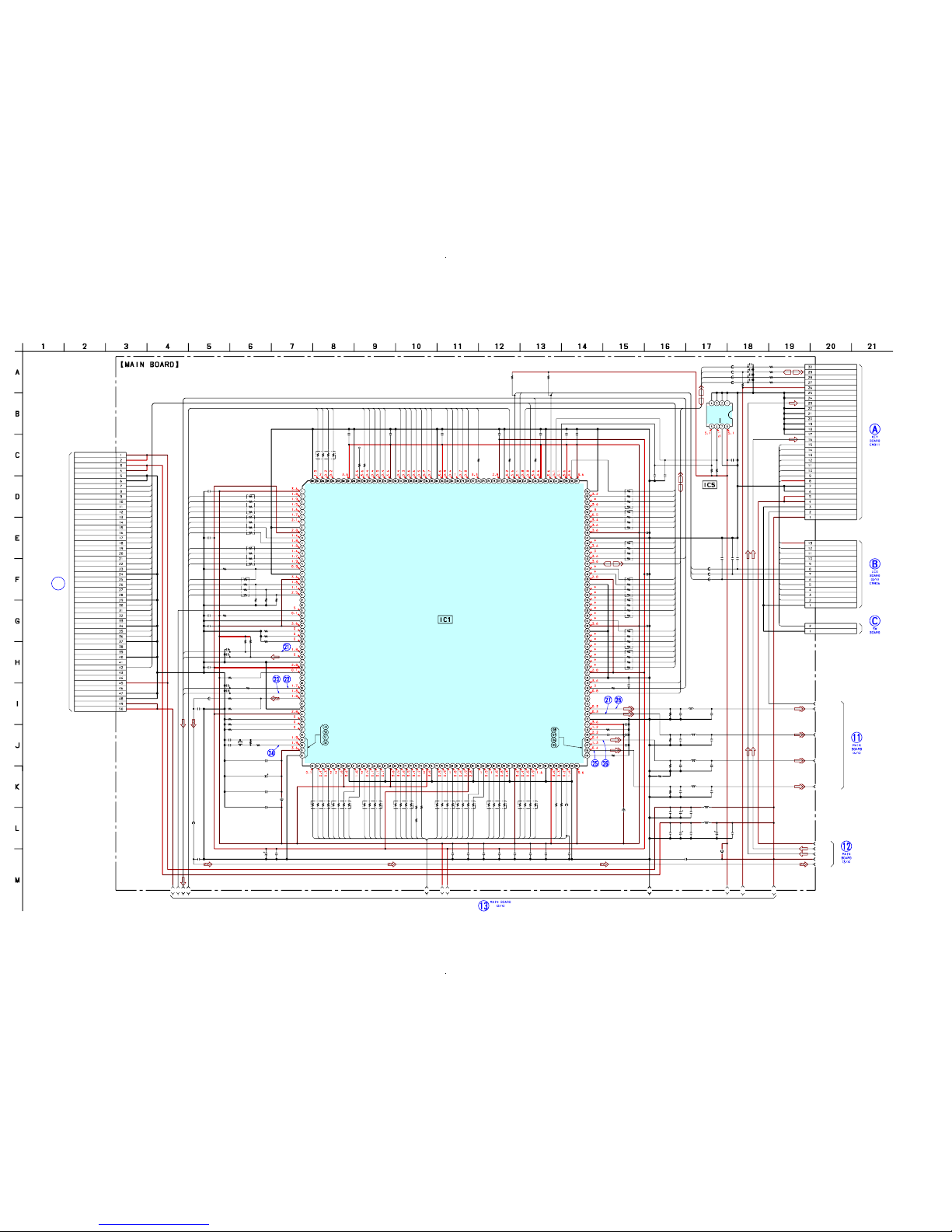
6-7. SCHEMATIC DIAGRAM – MAIN Board (1/4) –
• See page 39 for Waveforms. • See page 47 for IC Pin Function Description.
(Page 27)
(Page 28)
(Page 29)
(Page 38)
(Page 34)
(Page 38)
IC1
C23
RB1
R
B2
R
B
3
R
B
4
R
B
5
R
B
6
R
B
7
RB8
C24 C25 C26 C27 C28 C29 C30 C72
R
2
7
R
2
5
R
2
4
R
29
R
3
0
L309
C371 C369
C370
C366
CN104
CN103
CN102
R69
R70
R71
R72 C99
C157
C96
C97
R32
C32
R34
C66C68
C69C71C74C75
C78
R
4
3
R
4
4
R
42
R
40
R
3
9
RB21
R68 R66
R61 R62
C1
C2
C3
C4
R10 R11
C5
C6
C7
C8
C9
C10
C18
C19
C17
C21
RB17
RB18
R1
RB20
RB19
R2 R3 R4
R7
R8
R9
R12
R14
R16
R17
R19
R20
R21
CN101
R33
C52
C44
C89
C86
RB13
RB11
RB12
RB10
R31
C34
C33
C35
RB14
RB15
RB16
R76
R75
R74
R73
C100
R77
R5
IC
5
L3
C22
L7
L8
L9
L10
L11
L12
L55
C58
FB3
C98
C95
C79
C368
C367
L2
L1
L50
L40
L48
C15
C14 R22X1
L52
L
5
6
L51
C31
C373
C372
L308
R23
C134 C179
C87
C
105
C
15
1
C
1
0
6
C101
C102
C103
C104
ES6008FF
100p
10
1
0
1
0
3
3
1
0
1
0
1
0
10
0.1 0.1 0.1 0.1 0.1 0.1 0.1 15 p
0
3
3
3
3
10
10
1 0.1
100
16V
1
2P
13P
30P
75
75
75
75 470p
470p
470p
470p
270
0.1
33
0.10.1
0.10.10.10.1
0.1
33
33
33
33
3
3
10
10k 4.7k
1k 1k
0.1
0.1
0.1
0.1
4.7k 4.7k
100p
100p
0.1
100p
100p
330p
0.1
0.1
10
16V
0.1
10
10
4.7k
10
10
4.7k 4.7k 4.7k
100k
100k
100k
4.7k
33
4.7k
33
100k
100k
100k
50P
0
0.1
0.1
100p
0.1
33
33
33
33
0
0.1
10
16V
33p
33
33
33
33
33
33
33
470p
4.7k
4.7k
S
-2
4
C
S
02
A
FT
10
16V
0.1
470p
470p
470p
0.1
10
35V
11p
11p 100k27MHz
0.1
0.1
10
35V
1.5k
33p 100p
100p
33
p
33p
33
p
33p
33p
33p
33p
A
1
A
2
A
3
A
4
A
5
A
6
A
7
A
8
A
9
A
1
0
A
11
CVBS
Y
R-Y
B-Y
SW12V
LIGHT-PWEJ
SPDIF
+5V
IR-L
IR-R
L
A
0
L
A
1
L
A
2
L
A
3
L
D
0
L
D
1
L
D
2
L
D
3
L
D
4
L
D
5
L
D
6
L
D
7
L
D
8
L
D
9
L
D
1
0
L
D
1
1
L
D
1
2
L
D
1
3
L
D
1
4
L
D
1
5
L
C
S
3
#
L
O
E
#
W
R
L
L
AUX4
A
U
X
4
HRST
HRST
HD0
HD1
HD2
HD3
HD4
HD5
HD6
HD7
HD8
HD9
HD10
HD11
HD12
HD13
HD14
HD15
HD0
HD1
HD2
HD3
HD4
HD5
HD6
HD7
HD8
HD9
HD10
HD11
HD12
HD13
HD14
HD15
HIRQ
HIRQ
HA0
HA1
HA2
HA0
HA1
HA2
HIORDY
HIORDY
HWR#
HWR#
HRD#
HRD#
HCS1#
HCS1#
HCS3#
HCS3#
HIDCS16#
HIDCS16#
MCLK
A
U
X
3
AUX4 O
EAUX31
TBCK
TSDO
TWS
SCLK
SCLK
INS
INS
B
S
A
U
X
5
A
U
X
6
A
U
X
7
AUX6
AUX7
AUX2
A
U
X
2
C
L
K
D
Q
M
X
D
B
0
D
B
1
D
B
2
D
B
3
D
B
4
D
B
5
D
B
6
D
B
7
D
B
8
D
B
9
D
B
1
0
D
B
1
1
D
B
1
2
D
B
1
3
D
B
1
4
D
B
1
5
C
S
O
#
BS AUX5
RST
RST
IN
IN
EJ
EJ
A/D
A/D
CONT
CONT
TEMP
TEMP
REM
REM
VCC
VCC
SW
SW
H
A
4
H
A
5
H
A
6
H
A
7
H
A
8
H
A
9
H
A
1
0
H
A
1
1
C
K
E
W
E
#
C
A
S
#
R
A
S
O
#
H
A
0
H
A
1
H
A
2
H
A
3
B
A
N
K
0
B
A
N
K
1
SDIO
SDIO
LA4
LA5
LA6
LA7
LA8
LA9
LA10
LA11
LA12
LA13
LA14
LA15
LA16
LA17
LA18
LA19
+5V
+5V
+5V
+5V
GND
GND
RST
HD0
HD1
HD2
DH3
HD4
HD5
HD6
HD7
HD8
HD9
HD10
HD11
HD12
HD13
HD14
HD15
GND
HA1
HA2
GND
IORDY
IOWJ
IORJ
HCS1J
GND
HCS16J
HCS3J
GND
LOAD+
LOAD-
GND
SPD_DET
ENDSW
SLOT_OUT_DET
SLOT_IN_DET
PA5V
SPD_STP
GND
GND
SM8V
SM8V
HA0
HINTJ
V
C
C
S
C
L
SD
A
W
C
G
N
D
S
2
S
1
S
0
LA4
LA5
LA6
LA7
LA8
LA9
VSS
LA10
LA11
LA12
LA13
LA14
LA15
LA16
VSS
LA17
LA18
LA19
LA20
LA21
VSS
TDMDR
VSS
VSS
RSD
RWS
RBCK
NC
XIN
XOUT
D
M
A
0
D
M
A
1
D
M
A
2
D
M
A
3
D
M
A
4
D
M
A
5
V
S
S
D
M
A
6
D
M
A
7
D
M
A
8
D
M
A
9
D
M
A
1
0
D
M
A
1
1
V
S
S
V
S
S
D
B
0
D
B
1
D
B
2
D
B
3
D
B
4
D
B
5
V
S
S
D
B
6
D
B
7
D
B
8
D
B
9
D
B
1
0
D
B
1
1
V
S
S
D
B
1
2
D
B
1
3
D
B
14
D
B
1
5
V
S
S
D
Q
M
D
S
C
K
V
S
S
VSS
L
A
3
L
A
2
L
A
1
L
A
0
V
S
S
L
D
1
5
L
D
1
4
L
D
1
3
L
D
1
2
V
S
S
L
D
1
1
L
D
1
0
L
D
9
L
D
8
L
D
7
L
D
6
L
D
5
V
S
S
L
D
4
L
D
3
LD
2
L
D
1
LD
0
V
S
S
V
S
S
V
S
S
VSS
VSS
VSS
VSS
VSS
MS GND
MS GND
MS VEE
MS SCLK
MS INS
MS SDIO
IR LCH
IR GND
IR GND
IR GND
IR GND
IR GND
IR GND
IR RCH
RESET
REM
SW12V
SW12V
LED DISC IN
KEY PW/EJ
KEY A/D
TEMP DET
REM VCC
LIGHT GND
LIGHT GND
KEY GND
IR CONT
LIGHT PW/EJ
LIGHT KEY/GATE
REMVCC
REM
TEMP-DET
DA-BE
CK-BE
CS-BE
RESET
KEY GND
LED DISC IN
KEY PW/EJ
KEY A/D
IR CONT
MONITOR SW
MONITOR SW
SW GND
(1/4)
VEE
VCC
VEE
XRESET
TDMDX
VEE
TDMCLK
TDMFS
TDMTSC#
DAC LRCK
DAC DATA
VCC
SEL_PLL1
NC
NC
DAC MCLK
DAC BCK
SPDIF
NC
VCC
AVEE
AVSS
V
E
E
V
E
E
X
D
C
A
S
D
S
C
K
_
E
N
X
D
W
E
X
D
R
A
S
D
B
A
N
K
0
D
B
A
N
K
1
V
E
E
V
C
C
V
E
E
D
C
S
1
#
V
E
E
X
D
C
S
0
V
E
E
DCLK
R-Y
VREF C
B-Y
COMP
RSET
ADVEE
ADVSS
Y
VBS
YUV7
PCLK2XSCN
MS SCLK
MD
MS INS
VCC
HD0
HD1
HD2
HD3
HD4
HD5
HD6
VEE
HD7
HD8
HD9
HD10
HD11
HD12
HD13
VCC
HD14
HD15
MS SDIO
MC
HIRQ
XHRST
HIORDY
VEE
XHWR
XHRD
XHIOCS16
XHCS1FX
HCS3FX
HA0
HA1
VEE
H
A
2
V
E
E
S
D
A
S
C
L
D
A
-B
E
V
E
E
D
A
C
M
L
E
N
D
S
W
M
S
B
S
C
S
-B
E
CK
-B
E
X
L
O
E
V
C
C
X
L
C
S
0
X
L
C
S
1
X
L
C
S
2
X
L
C
S
3
V
EE
V
EE
X
L
W
R
H
L
V
EE
C
A
M
IN
0
C
A
M
IN
1
MS BS
EEPROM
MPEG DECODER
X
L
W
R
L
L
2.2µH
2.2µH
2.2µH
2.2µH
22µH
22µH
SERVO
BOARD
(2/3)
CN1
P
Ver 1.1
(Supplement-1
page 13)
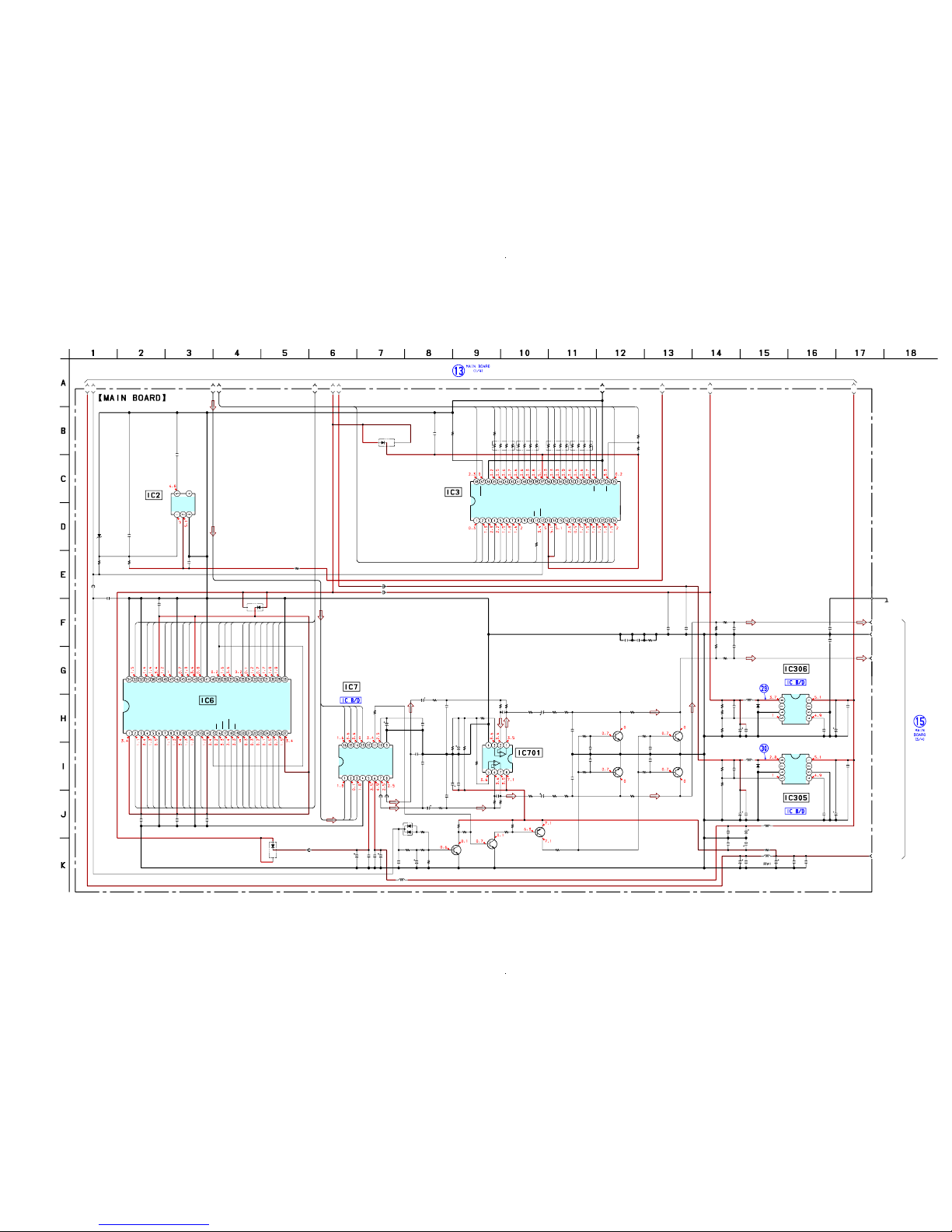
MV-900SDS
2727
MV-900SDS
6-8. SCHEMATIC DIAGRAM – MAIN Board (2/4) –
• See page 39 for Waveforms. • See page 41 for IC Block Diagrams.
(Page 28)
(Page 26)
Q701
Q702
Q703
Q704
C94
D12
C144
C143
L54
C701
R703
C702
R704
C705
R705
R706
C706
C707
R707
R709
R710
R711
R712
C708
C709
R713
R714
C710
C711
R715
R716
R719
R720
C712
C713
R722
R721
R723
R724
R725
R726
Q1
R81 R82
Q2
R83R84
Q3
D13
R85
R86
R87
R88
C149
R1733
R1734
R1709
R1710
C385
C384
L312
R377
C381
C379 L311 C376C377
C378
C382
C383
R370
R371
R372
C396
C394
C395
L314
D321
C393
C392
IC306
C400
R368
R369
C390
C391
C389
L313
D320
IC305
C388
C386
C387
R49
R90
R57
C84 R54
RB22
RB23
RB24
RB25
D14
C83
R48 C80 R46
C146
C145
R727
C90 C91
D1
IC6
R52
FB2
FB1
C791
C790
IC701
IC7
R78
C148
C147
L53
C92
L41
C82
R47
IC3
R708
IC2
R80
C81
C135
C150
C715
C714
C717
C716
C177 C178
C794 C795
C796
C797
C703
C704
L706
L707
C792
C793
2SC2412K
2SC2412K
2SC2412K
2SC2412K
0.1
RB491D-T146
47
16V
0.1
1
50V
22k
1
50V
22k
10
16V
47k
47k
220
16V
0.1
3.3k
3.3k
3.3k
22k
22k
150p
150p
1k
1k
10
16V
10
16V
000
0
100p
100p
4.7k
4.7k
470
470
4.7k
4.7k
2SA1037AK
3.3k 100k
2SC2412K
33k33k
2SC2412K
DAN202K
220k
120k
47
220k
100p
0
0
47k
47k
0.1
100
16V
150
100
16V
0.1
0.10.1
220
16V
100
16V
1000p
56k
22k
1.2k
470p
0.1
470
16V
RB161L-
10TE25
4700p
10
16V
XC63778103SR
0.1
18k
10k
470
16V
2200p
0.1
RB161L-
10TE25
XC63778103SR
4700p
10
16V
0.1
0
4.7k
0
0.1 0
10
10
10
10
RB491D-T146
0.022
10k 0.1 0
47
16V
0.1
0
0.1 0.1
RB491D-T146
HY57V641620HGTP
-HI
0
100p
100p
RC45580R
PCM1751DBQR
33k
0.1
10
16V
1
1000p
0
MBM29LV800TA
-70PFTN
3.3k
PST3645NR
10k
MA8068-L-TX
33p
10
35V
0.1
0.1
0.1
0.1
100p 100p
4700p 4700p
4700p
1000p
1000p
1000p
100p
100p
A1
A2
A3
A4
A5
A6
A7
A8
A9
A10
A11
L-CH_AUDIO
R-CH_AUDIO
AUDIO_GND
+8V
LA0
LA1
LA2
LA3
LA4
LA5
LA6
LA7
LA8
LA9
LA10
LA11
LA12
LA13
LA14
LA15
LA16
LA17
LA18
LA19
LD0
LD1
LD2
LD3
LD4
LD5
LD6
LD7
LD8
LD9
LD10
LD11
LD12
LD13
LD14
LCS3#
LOE#
WRLL
AUX3
AUX4 O
MCLK
EAUX31
TBCK
TSDO
TWS
HA4
HA5
HA6
HA7
HA8
HA9
HA11
CKE
CLK
DQMX
DB8
DB9
DB10
DB11
DB12
DB13
DB14
DB15
HA0
HA1
HA2
HA3
HA10
DB0
DB1
DB2
DB3
DB4
DB6
DB5
DB7
CSO#
WE#
CAS#
RASO#
BANK1
BANK0
OUT
VDD
GND
CD NC
SCK
ML
MC
MD
ZEROL
ZEROR
VCOM
AGND
VOUTR
VOUTL
VCC
VDD
DGND
LRCK
DATA
BCK
VSS
DQ15
VSSQ
DQ14
DQ13
VCCQ
DQ12
DQ11
VSSQ
DQ10
VCC
DQ0
VCCQ
DQ1
DQ2
VSSQ
DQ3
DQ4
VCCQ
DQ5
DQ6
DQ9
VCCQ
DQ8
VSS
NC
DQMH
CLK
CKE
NC
A11
A9
A8
A7
A6
A5
A4
VSS
VSSQ
DQ7
VCC
DQML
WE
CAS
RAS0
CS
BA0
BA1
A10
A0
A1
A2
A3
VCC
A15
A14
A13
A12
A11
A10
A9
A8
VPP
WP#
BY#
A18
A17
A4
A6
A5
A4
A3
A2
A1
WE
RST
A0
GND
DQ0
DQ8
DQ1
DQ9
DQ2
DQ10
DQ3
DQ11
VCC
DQ4
DQ12
DQ5
DQ13
DQ6
DQ14
DQ7
DQ15
GND
A16
BYTE
OE
CE
VIN
EXT2
PBST
CE
LX
EXT1
GND
VOUT
VIN
EXT2
PBST
CE
LX
EXT1
GND
VOUT
(2/4)
SWITCHING REGULATOR
SWITCHING REGULATOR
MUTING
Q701-704
Q1,2
MUTING SWITCH
LOW-PASS
FILTER
DELAY
D/A CONVERTER
FLASH ROM
SD-RAM
GND
VCC
RESET SIGNAL
GENERATOR
(CHASSIS)
100µH
100µH
22µH
22µH

MV-900SDS
2828
MV-900SDS
6-9. SCHEMATIC DIAGRAM – MAIN Board (3/4) –
• See page 38 for Waveforms. • See page 41 for IC Block Diagrams.
(Page 38)
(Page 26)
(Page 27)
(Page 29)
IC304
C346 C345
C344
Q324
R365
Q323
R366
R367
R364
C201
C202
C203
C204
R205
R206
Q201
Q202
Q203
Q204
Q207
C231 C232
R227 R228 R229 R230
Q210 Q211 Q212 Q213
D317
R223
R224
R225
R226
C230
C229
C226
C227 C228
X201
C213
C223
C224R218R217
C222
R219
R213 C220
R214
R215
R216C219
C211
C210
C209
FL201R221C225
D204
L202
R212
IC704
IC705
R231
D201
C221
C731
C718
C719
R752
L350
C737
C738
C735
C736
C733
C734
R755
C732
R754
R751
R750
R746
R747
R749
C724
C725
C727
C722R744
R745
R741
R740
R737
R738
R739
R735
C720
C721
R742
R734
R730
R731
D315D316
L304 L303
Q302
Q303
R302 R301
C305
C304
L302
C315
C316
R307
R309
C317
R310
C318
Q208
Q209
Q305
Q306
R311
L306
D306
R333
R332 R331
Q313
R330
C348 R324
R326
R325
C350
R327
R323 C331
R321
R322
Q314
R328
C332
R329
C333
Q311
Q309
R379
R378 R380
R381
C328
R318
R317
R319
C327
Q310
L305
D308
D307
R320 C349
R308
C217
C218
R211
C214 R232
C216
R209
C330
R304 C306
C307
R303
R305
R306
R753
R736
R743
L201
IC201
IC301
C329
C351R315R316C326
C347
Q312
Q304
R313
R314
C324
C325 R312 C321
C320
D314
C310
C309C314
C313
Q301
J301
Q205
Q206
D304 D303
C212
D203 D202
CN201
IC703
C723
R334 D305
R220
CN701
F301
F302
L203
L701
L702
L703
R210
R201
R202
R204
R203
R207
R208
C215
C726
R748 C730
D302
C253
C251
C252
XC6202P502PR
0.1 0.1
22
16V
2SA1797
10k
2SC4081
22k
47k
10k
1
1
4700p
4700p
3.3k
3.3k
DTC144EUA
DTC144EUA
DTC144EUA
DTC144EUA
DTC144EUA
150p 2200p
4.7k 4.7k 4.7k 4.7k
DTC144EUA DTC144EUA DTC144EUA DTC144EUA
DAN202K
100
100
100
100
22p
22p
100
16V
0.01 0.1
7.6MHz
0.01
10p
82p3.3k3.3k
2200p
10k
220 33
10V
2.2k
4.7k
1.5k1
10
35V
150p
2200p
1500.1
1SS356
10k
NJM2233
NJM2233
10
KV1471ETR
0.047
1
10
35V
10
35V
22k
0.1
100
16V
10
35V
10
35V
0.01
100
16V
1k
47
16V
1k
22k
22k
12k
12k
12k
4.7
25V
4.7
25V
4.7
25V
100p100k
100k
2.2k
2.2k
10k
10k
10k
47k
100p
100p
100k
47k
0
0
1SS3551SS355
2SC4081
2SA1576A
220 2.2k
0.01
470
25V
470
25V
0.01
2.2k
220
100p
220
100p
2SK209GR
2SC4081
2SC4081
2SA1576A
47
1SS355
1k
1k 47k
2SA1576A
220
0.01 10k
39k
39k
470p
47k
18k 0.47
39k
470k
2SA1576A
47k
2.2
22k
1
2SC4081
2SA1797
4.7k
47k 4.7k
22k
10
35V
27k
39k
18k
0.47
2SA1576A
1SS355
1SS355
47k 2.2
10k
10
35V
330p
10k
33p 33
0.01
18k
470p
47 100p
100p
220
15k
82k
22k
10k
100k
100nH
BH1415F
BA9743AFV
0.15
470p39k22k220p
470p
2SC4081
TPC6102
68k
22k
10
35V
1000p 20k 0.01
2200
25V
RB050-40TE25
0.01
470
25V
2200
25V
0.01
TPC6102
DTA144EUA
DTA144EUA
UDZS5.6B UDZS5.6B
1
1SS356 1SS356
3P
RC45801PWR
100p
1k 1SS355
6.8k
7P
2A 72V
1A
72V
2.2k
2.7k
2.7k
2.2k
2.2k
10k
10k
1000p
4.7
25V
12k 1
RB050L-40TE25
4700p
C255
4700p
C254
4700p
4700p
4700p
B1
B2
B3
B4
B5
B6
B7
B8
B9
B10
B11
L-CH_AUDIO
R-CH_AUDIO
AUDIO_GND
IR-L
IR-R
SW12V
SPDIF
+8V
+5V
FM-DATA
FM
-CLK
FM-CE
FM2
FM1
+5V REGULATOR
VCC
XOUT
XIN
CE
CLK
DATA
ATT
SEP
LLPF
LEMP
LIN
RFOUT
RFGND
VTIN
VCC
PD
GND
VC
RLPF
REMP
RIN
MPX ADJ
GND
VCC
GNDVIN1
SWI
VIN2
NC
VOUT
V+
NC
GNDVIN1
SWI
VIN2
NC
VOUT
V+
NC
R+
R-
L-
L+
VGND
VIN
AUDIOGND
CT
CR
NON1
INV1
FB1
DT1
OUT1
GND
VREF
SCP
NON2
INV2
FB2
DT2
OUT2
VCC
S
S
S
(3/4)
AUDIO INPUT SELECT
AUDIO INPUT SELECT
Q208,209
LOW-PASS
FILTER
OGI
Q210-213
LEVEL SHIFT
FM MODULATOR
ANTENNA
FM STEREO
MODULATOR
POWER CONTROL
B+ SWITCH
Q309,311
DEAD
TIME
SWITCHING
LATCH
B+ SWITCH
Q323,324
REGULATOR
CONTROL
Q305,306
REGULATOR
SWITCHING
REGULATOR
CONTROL
Q302,303
REGULATOR
SWITCHING
OPTICAL
TRANSCEIVER
SPDIF
5V
GND
OPTICAL
OUTPUT
INVERTER BUFFER
BUFFER
Q201-204
RF LEVEL
SWITCHING
DIFFERENTIAL
AMP
2.2µH
22µH
22µH
22µH
22µH
22µH
100µH

MV-900SDS
2929
MV-900SDS
6-10. SCHEMATIC DIAGRAM – MAIN Board (4/4) –
• See page 41 for IC Block Diagrams.
(Page 28)
(Page 26)
(Page 34)
(Page 32)
(Page 32)
(Page 38)
CN705C762 C764
C757
D701
1SS133
C761 C763
Q711
C755 C756
C752
R778
R779
C751
R776
R777
C758
C749
C750
Q709
Q708
R782
R783
R784
R785
R781
R774
R775
C748
C747
R770
R771
C771
C772
R795
R792
Q713
Q712
R798
R799
C773
C774
R1701
R1702
C775
C776
R345 R343
C343
R344
Q322
Q321
R342
C765
R796
R797
R786
R787
C769
C770
R788
R789 R791 R793
C767
C768
R790 R794
IC708
R763
R764
R765
C743
R766
C746
C745
R769
R357
R361
R356
R352R351
L307
Q319
R360R359
R362
Q320
C365
R355
C364
C363
D318
R354
Q316
R353
C362
D312 R358
Q325
TH301
R384
Q326
CN108
CN107
Q315
D310
R340
IC102
C174
IC101
R107
R108
C165
R103
C766
R109
R110
R111
C340
C341
IC303
Q317
IC302
C338
C337 C336
C335
Q307
Q308
R337
R338
R335
R336
CN302
C301
C302 C303 D301
R768
R767
R386
C397
R341 C339
R385
D313
R339
R383
R773
R772
C342
C168
C166
C167
R104
R106C172
R761
IC707
S301
CN105
L301
C398
Q318
R105
IC706
M301
CN702
SP1
SP2
C162
C161
L101
C173
C169
C170
C171
R762 C744
CN301
D309
L704
L705
C759
F304
C175
C176
VDR301
Q710
R1765 R1766
Q714
Q715
R1767 R1768
R1769
F303
4P1000 10V 1000 10V
10
35V
1000
10V
1000
10V
2SA1576A
100
16V
4.7
25V
1
2.2k
2.2k
1
10k
10k
0.1
0
0
DTC314TU
DTC314TU
10k
4.7k
1k
10k
10k
10k
10k
111k
1k
4.7
25V
4.7
25V
100
100
DTC314TU
DTC314TU
22k
22k
100p
100p
100
100
10
35V
10
35V
10k 10k
47
25V
47k
2SC4081
2SB1694
1k
4.7
25V
2.2k
2.2k
4.7k
4.7k
47
25V
0.1
10k
10k 6.8k 12k
100p
100p
6.8k 12k
NJM4558V
4.7k
6.8k
6.8k
10
35V
100
0.01
220
16V
4.7k
0
100k
15k
22k3.3k
2SB1694
100k10k
10k
2SC4081
47
25V
15k
1
50V
2.2
DAN202K
10k
2SC4081
22k
220
25V
1SS356 0
TPC6102
150k
2SC4081
10P
8P
2SC2412K
MA8068-L
10k
NJM2283V
0.1
MM1508
75
75
470
16V 75
4.7
25V
0
0
0
47
25V
0.1
TA78DL08AF
2SC4081
NJM78L12UA-TEJ
47
25V
0.1 0.1
22
16V
2SC4081
2SA1797
10k
22k
10k
47k
2P
2200
25V
0.01 100 1N5404TU
4.7k
100
22k
47
16V
4.7k 0.1
150k
UDZS5.6B
4.7k
0
100k
100k
10
35V
10
35V
100
16V
0.01
75
750.1
10
LA4627
11P
0.15
2SA1576A
75
PT2257
6P
10 35V
10 35V
10 35V
10
35V
10 35V
10 35V
4.7k 10
35V
4P
UDZS-308
22
16V
1A
10
35V
10
35V
2SC4081
10k 10k
2SC4081
2SC4081
10k 4.7k
680
5A
B1
B2
B3
B4
B5
B6
B7
B8
B9
B10
B11
CVBS
Y
R-Y
B-Y
LIGHT-PWEJ
S
-S
D
K
S
-S
D
A
S-SDA
S-SCK
FM-CE
FM-DATA
FM-CLK
FM2
FM1
LIN
DC
P.P
NC
LOUT
VCC
NC
ROUT
STBY
RINNCPRE
GND
POWER
GND
POWER
GND
RCH
AUDIOGND
AUDIOGND
LCH
VGND
VOUT
LIN
1
LO
U
T1
V
C
C
C
LK
R
IN
1
R
O
U
T1
G
N
D
D
AT
A
GND
GND
GND
GND
BATT
BATT
BATT
BATT
FM-DATA
FM-CE
S-SCK
S-SDA
A MUTE
SW1
FM1
FM2
AMP ON
POWER ON
FM-CLK
FAN CONT
ACC IN
ACC SW
LIGHT PW/EJ
V GND
Y/CVBS
V GND
R-Y
V GND
B-Y
ACC
BATT
AMP REN
BATT GND
V+
IN2B
GNDI
IN1A
SW2
IN2A
GND3
IN3B
IN1B
SW1
OUT1
GND2
OUT2
OUT3
SW3
IN3A
V+VIN2
GND
VIN1
VOUT
SW
+12V REGULATOR
FAN+
FAN-
+8V REGULATOR
S
(4/4)
GND
VCC
LINE AMP
POWER AMP
Q710,711
STANDBY SWITCH
MUTING
MUTING
MUTING
MUTING
MUTING
Q321,322
POWER ON
B
A
POWER
SELECT
ACCESSORY
DETECT
Q325,326
B+ SWITCH
B+ SWITCH
Q307,308
Q319,320
POWER ON
MUTING
MUTING SWITCH
MUTING
CONTROL
Q316,317
VIDEO INPUT SELECT
VIDEO INPUT SELECT
ELECTRICAL
VOLUME
(FAN)
OGI
OGI
(L-CH)
(R-CH)
GND
GND
AMP REM
ACC
BATT
Q714,715
DISCHARGE SWITCH
22µH
47µH
9
876 321
10 11 14 15 16

MV-900SDS
3030
MV-900SDS
6-11. PRINTED WIRING BOARD – LCD Board (Side A) –
• See page 23 for Circuit Boards Location.
: Uses unleaded solder.
(Page 24) (Page 24)
(Page 24) (Page 24)
R514
R515
C541
R507
R612
R610
R608
R607
R606
11236
25
2413
3748
IC601
R603
R601
R643
R630
R621
R619
R620
R662
R830
R849
R832
R833
C813
R801
C864
R870
R869
R868
R842
R829
R841
C836
C837
C845
FL603
FL602
FL601
C606
R633
C657
C658
R609
R604
R602
R614
R615
R616
R617
R618
R611
R642
R639
R638
R637
R661
R660
C609
R525
R518
C533
R517
R516
C532
ECB
Q503
ECB
Q502
R540
R538
R539
R537
C502
C514
C546C547
L502
L606
L503
L601
L604
L605
L812
L803
L603
L602
L501
L402
X502 X501
Q603
BCE
C531
+
C536
+
C511
+
C483
+
C481
+
C544
+
C513
+
C507
+
C512
+
C520
+
C505
+
C504
+
C517
+
C516
+
C529
+
C525
+
C515
+
C522
+
C501
+
C608
+
C604
+
C660
+
D602
KA
RV601
IC401
IC403
C610
C659
CN908
10
CN909
8
1
NC
1
CN907
L950
81
CN905
11 1
CN906
13 1
R450 R494
R402
R404
R406
R473
R408
R411
R412
R413
R416
R417
R495
R955
R496
R479
R403
R405
R407
R449
R472
R447
R448
R446
R444
R442
R439
R432
R445
R443
R440
R438
R460 R434
R477 R427
R461
R462
R426
R425
R423
C963
C412
R422
C956
F801
R964
R959
R960
R956
R421
R420
R419
R418
R424
R435
R471
R498
R497
R429
R492 R470
R493
R456
R455
C409
C407
R433
C551
R430
1
13
2
16
17
32
54
49
48 33
ECB
ECB
Q403
Q402
ECB
Q401
Q953
Q955
D402
AK
D955
AK
D956
D954
AK
AK
D950
AAAK
K
BCE
BCE
D801
C959
+
C816
+
C817
+
C829
+
C957
+
C405
+
C850
+
C955
+
C851
+
C852
+
C859
+
C860
+
L850
L851
L852
CN801
C833
+
C820+C819
+
C841
+
C839
+
C831
+
C823+C822
+
C827
+
C826+C825
+
C806
+
C809
+
C835
+
D804
D803
AK
AK
D802
AK
RV802
C844
C838
+
T801
DC/DC CONVERTER
C962
+
C954
C805
D851
KA
L801 L802
F850
R499
R864
R865
R866
RV803 RV801
K
D852
CN850
T850
INVERTER
TRANSFORMER
LCD BOARD
(SIDE A)
1-863-447-
S403
S402
S401
S404
12
A
BACK LIGHT
UNIT
130
LCD1
LIQUID CRYSTAL
DISPLAY MODULE
TP853
VOL +
VOL –
REVERSE
MENU
MAIN
BOARD
CN107
G
MAIN
BOARD
CN103
B
MAIN
BOARD
CN105
H
MAIN
BOARD
CN108
F
(11)
11
A
B
C
D
E
F
G
H
I
1 2 3 4 5 6 7 8 9 10 11 12 13 14 15 16
A/K
Ref. No. LocationRef. No. Location
D402 C-10
D602 F-7
D801 E-10
D802 G-11
D803 G-11
D804 F-11
D851 D-12
• Semiconductor Location
Ref. No. Location Ref. No. Location
D852 G-14
D950 E-11
D954 D-9
D955 D-9
D956 D-9
IC401 C-8
IC403 B-9
IC601 G-6
Q401 B-9
Q402 B-9
Q403 B-9
Q502 H-3
Q503 H-4
Q603 H-6
Q953 C-10
Q955 C-10
 Loading...