

Page 1
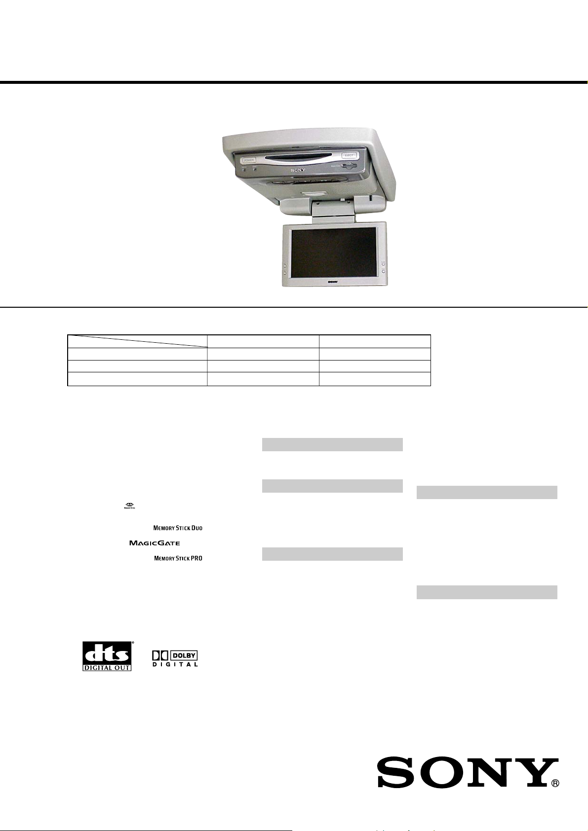
MV-900SDS
SERVICE MANUAL
Ver. 1.3 2005.10
COMPONENT MODEL NAME
MODEL NUMBER LABEL PRINTED MODEL NAME
DVD PLAYER MV-900SDS XVM-R90D
CORDLESS STEREO HEADPHONE MDR-IF0140 MDR-IF0140
CARD REMOTE COMMANDER – RM-X137
US Model
Copyrights
This product incorporates copyright protection
technology that is protected by method claims
of certain U.S. patents, other intellectual
property rights owned by Macrovision
Corporation, and other rights owners. Use of
this copyright protection technology must be
authorized by Macrovision Corporation, and is
intended for home and other limited viewing
uses only unless otherwise authorized by
Macrovision Corporation. Reverse engineering
or disassembly is prohibited.
• “Memory Stick,”
Memory Stick” are trademarks of Sony
Corporation.
• “Memory Stick Duo” and “
are trademarks of Sony Corporation.
• “MagicGate” and “
trademarks of Sony Corporation.
• “Memory Stick PRO” and “
are trademarks of Sony Corporation.
Manufactured under license from Dolby
Laboratories. “Dolby”, “Pro Logic”, and the
double-D symbol are trademarks of Dolby
Laboratories.
“DTS,” “DTS Digital Surround” and “DTS
Digital Out” are trademarks of Digital Theater
Systems, Inc.
and “MagicGate
” are
SPECIFICATIONS
DVD player XVM-R90D
System
Laser Semiconductor laser
Signal format system NTSC/PAL
Audio characteristics
Frequency response 20 Hz to 20 kHz
Signal to noise ratio 90 dB (A)
Harmonic distortion 0.05 %
Dynamic range 90 dB
”
”
Wow and flutter below measurable limits
(±0.001% W PEAK)
General
Outputs FM output
Inputs Audio input
Power requirements 12 V DC
Dimensions Approx. 285 × 73 × 455 mm
Mass Approx. 3.5 kg
Operating temperature 0 °C to 45 °C
Audio output
Video output
Optical output
Video input
DC 12V input
1
/4 × 2 7/8 × 18 in)
(11
(w/h/d)
(7 lb 12 oz)
(32 °F to 113 °F)
Supplied accessories Card remote commander
RM-X137
Power supply cord (1)
RF modulator cable (1)
Mounting plate (1)
Screws (5)
Tapping screws (8)
Operating Instructions (1)
Monitor
System Liquid crystal color display
Display Manual flipdown panel
Drive system TFT-LCD active matrix
Picture size 9 inches wide screen (16:9)
Picture segment 336,960 (w 1,440 × h 234)
Cordless Stereo Headphones
MDR-IF0140
system
dots
General
Modulation system Frequency modulation
Carrier frequency Right 2.8 MHz
Frequency response 18 − 22,000 Hz
Power source DC 1.5 V (size AAA) dry
Mass Approx. 125 g (4.41 oz)
Operating temperature 5 °C to 35 °C
Design and specifications are subject to change
without notice.
Left 2.3 MHz
battery
including battery
(41 °F to 95 °F)
9-877-871-04
2005J05-1
© 2005.10
MOBILE DVD SYSTEM
Sony Corporation
e Vehicle Group
Published by Sony Engineering Corporation
Page 2
MV-900SDS
CAUTION
The use of optical instruments with this
product will increase eye hazard.
CAUTION
Use of controls or adjustments or performance of procedures
other than those specified herein may result in hazardous radiation
exposure.
Notes on chip component replacement
• Never reuse a disconnected chip component.
• Notice that the minus side of a tantalum capacitor may be
damaged by heat.
Flexible Circuit Board Repairing
• Keep the temperature of the soldering iron around 270 ˚C
during repairing.
• Do not touch the soldering iron on the same conductor of the
circuit board (within 3 times).
• Be careful not to apply force on the conductor when soldering
or unsoldering.
DANGER INVISIBLE LASERRADIATIONWHEN OPEN.
This is located on the drive unit's internal
chassis.
AVOID DIRECT EXPOSURE TO BEAM.
TABLE OF CONTENTS
1. SERVICING NOTES ................................................ 3
2. GENERAL
Location of Controls........................................................ 5
3. DISASSEMBLY
3-1. Disassembly Flow ........................................................... 9
3-2. Bracket (Main) ................................................................ 9
3-3. DVD Mechanism Deck Block ......................................... 10
3-4. MAIN Board.................................................................... 10
3-5. Rear Cover (Hinge) ......................................................... 11
3-6. LCD Block ...................................................................... 11
3-7. LCD Board ...................................................................... 12
3-8. Liquid Crystal Display Panel (LCD1) ............................. 12
4. TEST MODE.............................................................. 13
5. ELECTRICAL ADJUSTMENTS ......................... 14
6. DIAGRAMS
6-1. Block Diagram – MPEG DECODER Section – ............ 19
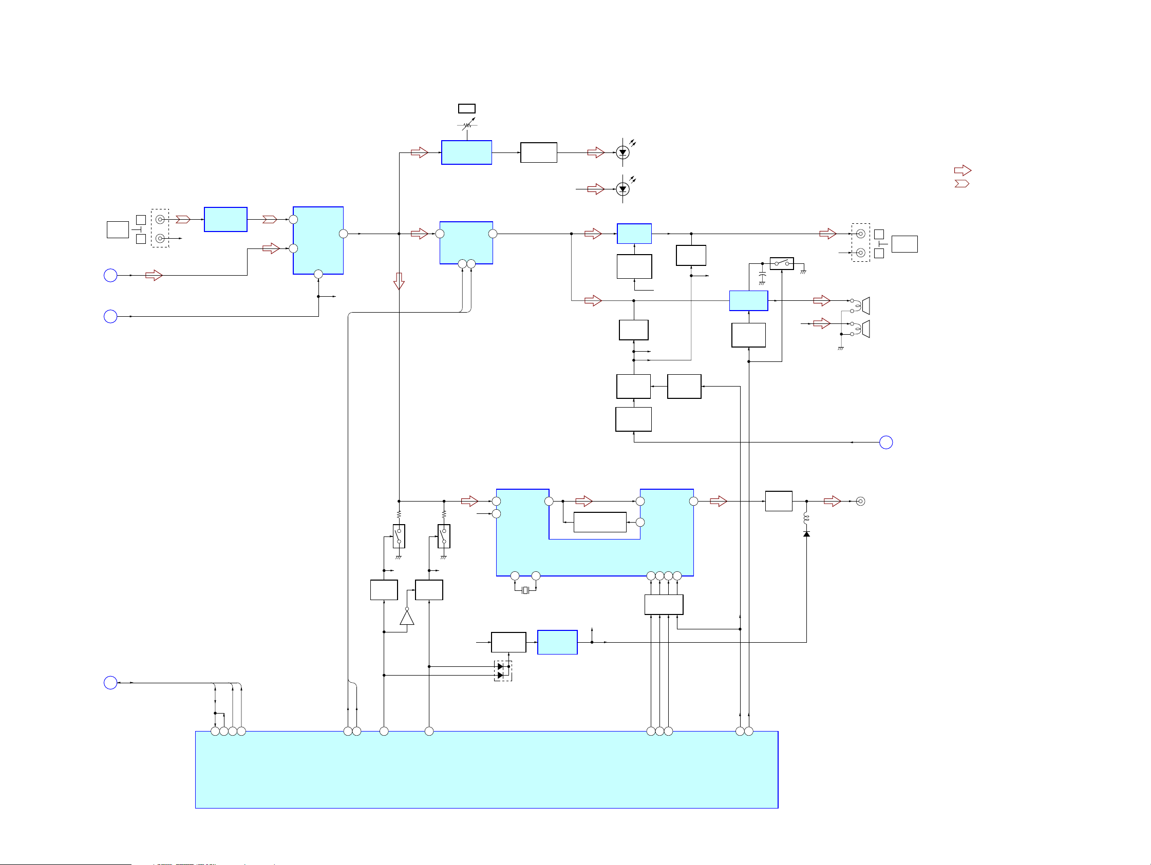
6-2. Block Diagram – AUDIO Section – ............................... 20
6-3. Block Diagram – VIDEO, PANEL Section –................. 21
6-4. Block Diagram – POWER SUPPLY Section – .............. 22
6-5. Printed Wiring Board
– MAIN Board (Component Side) – ............................... 24
6-6. Printed Wiring Board
– MAIN Board (Conductor Side) – ................................. 25
6-7. Schematic Diagram – MAIN Board (1/4) – ................... 26
6-8. Schematic Diagram – MAIN Board (2/4) – ................... 27
6-9. Schematic Diagram – MAIN Board (3/4) – ................... 28
6-10. Schematic Diagram – MAIN Board (4/4) – ................... 29
6-11. Printed Wiring Board – LCD Board (Side A) – ............. 30
6-12. Printed Wiring Board – LCD Board (Side B) – ............. 31
6-13. Schematic Diagram – LCD Board (1/4) – ...................... 32
6-14. Schematic Diagram – LCD Board (2/4) – ...................... 33
6-15. Schematic Diagram – LCD Board (3/4) – ...................... 34
6-16. Schematic Diagram – LCD Board (4/4) – ...................... 35
6-17. Printed Wiring Board – PANEL Section (1/2) – ............ 36
6-18. Printed Wiring Boards – PANEL Section (2/2) – ........... 37
6-19. Schematic Diagram – PANEL Section –........................ 38
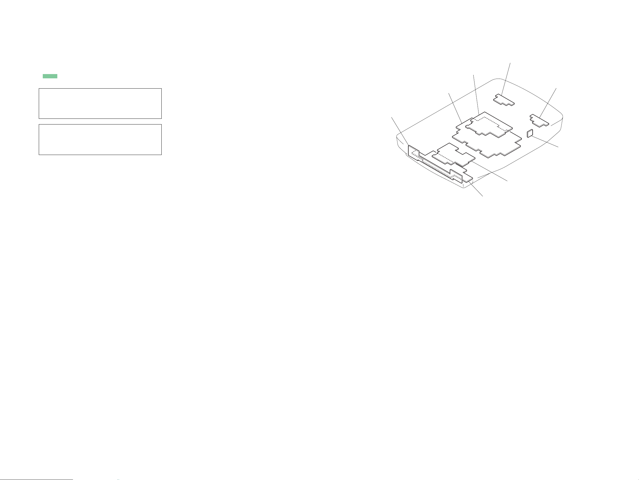
7. EXPLODED VIEWS
7-1. Skirt (Cabinet) Section .................................................... 54
7-2. Front (Panel) Section ....................................................... 55
7-3. MAIN Board Section....................................................... 56
7-4. Cabinet (Base) Section .................................................... 57
7-5. LCD Section.................................................................... 58
8. ELECTRICAL PARTS LIST................................ 59
2
Page 3

SECTION 1
SERVICING NOTES
MV-900SDS
NOTES ON HANDLING THE OPTICAL PICK-UP
BLOCK OR BASE UNIT
The laser diode in the optical pick-up block may suffer electrostatic
break-down because of the potential difference generated by the
charged electrostatic load, etc. on clothing and the human body.
During repair, pay attention to electrostatic break-down and also
use the procedure in the printed matter which is included in the
repair parts.
The flexible board is easily damaged and should be handled with
care.
NOTES ON LASER DIODE EMISSION CHECK
Never look into the laser diode emission from right above when
checking it for adjustment. It is feared that you will lose your sight.
UNLEADED SOLDER
Boards requiring use of unleaded solder are printed with the leadfree mark (LF) indicating the solder contains no lead.
(Caution: Some printed circuit boards may not come printed with
the lead free mark due to their particular size)
: LEAD FREE MARK
Unleaded solder has the following characteristics.
• Unleaded solder melts at a temperature about 40 ˚C higher
than ordinary solder.
Ordinary soldering irons can be used but the iron tip has to be
applied to the solder joint for a slightly longer time.
Soldering irons using a temperature regulator should be set to
about 350 ˚C.
Caution: The printed pattern (copper foil) may peel away if
the heated tip is applied for too long, so be careful!
• Strong viscosity
Unleaded solder is more viscou-s (sticky, less prone to flow)
than ordinary solder so use caution not to let solder bridges
occur such as on IC pins, etc.
• Usable with ordinary solder
It is best to use only unleaded solder but unleaded solder may
also be added to ordinary solder.
3
Page 4
MV-900SDS
About discs this player can
play
This player can play the following discs:
• DVD
• DVD-R/DVD-RW
• Video CD
• Audio CD
• CD-R/CD-RW
Disc type Label on the disc
DVD VIDEOs
Video CDs
Audio CDs
MP3 files/
JPEG files
“DVD VIDEO,” “DVD-R” and “DVD-RW” are
trademarks.
Region code of DVDs this player
can play
This player has a region code printed on the
rear of the player and will only play DVDs that
are labeled with identical region codes. DVDs
ALL
labeled
will also be played on this player.
If you try to play any other DVD, the message
“REGION ERROR” will appear on the screen.
Depending on the DVD, the region code
indication may not appear even if the DVD is
prohibited by area restrictions.
Region
code
Cautions
• This player CANNOT play these discs.
— DVD-Audio — DVD-RAM
— DVD-ROM — CD-G
— SVCD — CD-I
— Photo-CD — VSD
— Active-Audio (Data)
— CD-Extra (Data)
— Mixed CD (Data)
— CD-ROM (the data other than the MP3/JPEG
file)
— DVD-RW recorded in VR mode
• This product incorporates copyright protection
technology that is protected by method claims of
certain U.S. patents and other intellectual
property rights owned by Macrovision
Corporation and other rights owners. Use of this
copyright protection technology must be
authorized by Macrovision Corporation, and is
intended for home and other limited viewing
uses only unless otherwise authorized by
Macrovision Corporation. Reverse engineering or
disassembly is prohibited.
Note on PBC (Playback Control)
Notes on CD-Rs (recordable CDs)/
CD-RWs (rewritable CDs)/DVD-Rs
(recordable DVDs)/DVD-RWs
(rewritable DVDs)
• Some CD-Rs/CD-RWs/DVD-Rs/DVD-RWs
(depending on the equipment used for its
recording or the condition of the disc) may
not play on this player.
• You cannot play a CD-R/CD-RW/DVD-R/
DVD-RW that is not finalized*.
• You cannot play a CD-R/CD-RW that is
recorded in Multi Session.
• You can play MP3/JPEG files recorded on
CD-ROMs, CD-Rs, and CD-RWs.
* A process necessary for a recorded CD-R/CD-RW
disc to be played on the audio CD player.
4
This player conforms to Ver. 1.1 and Ver. 2.0 of
Video CD standards. You can enjoy two kinds
of playback according to the disc type.
Disc type
Video CDs without
PBC functions
You can
Video playback (moving
pictures) as well as music.
(Ver. 1.1 discs)
Video CDs with
PBC functions
(Ver. 2.0 discs)
• Interactive software
with menu screens
displayed on the
monitor.
•Video playback
functions.
• High-resolution still
pictures if they are
included on the disc.
Page 5
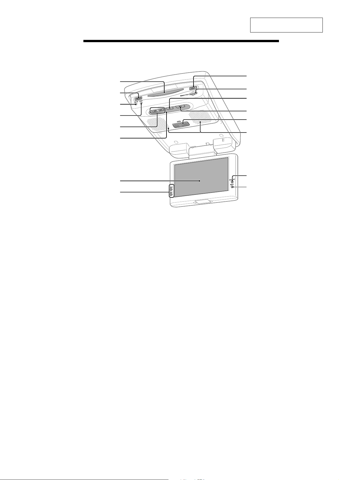
Location of controls
SECTION 2
GENERAL
MV-900SDS
This section is extracted from
instruction manual.
1
2
3
4
5
6
7
8
Refer to the pages listed for details.
1 Disc slot
2 POWER (on/off) button
To turn on/off the player.
3 DISC IN light
When a disc is in the player, the DISC IN
light glows orange.
4 RESET button
5 . (previous)/> (next) buttons
6 Receptor for the card remote
commander/Transmitter for the cordless
headphones
7 Monitor
8 VOL +/– buttons
To turn up or down the volume or to select
the item during menu operation.
9 EJECT button
Available to eject a disc from the player
even when the player is turned off.
9
0
qa
qs
qd
qf
qg
qh
XVM-R90D
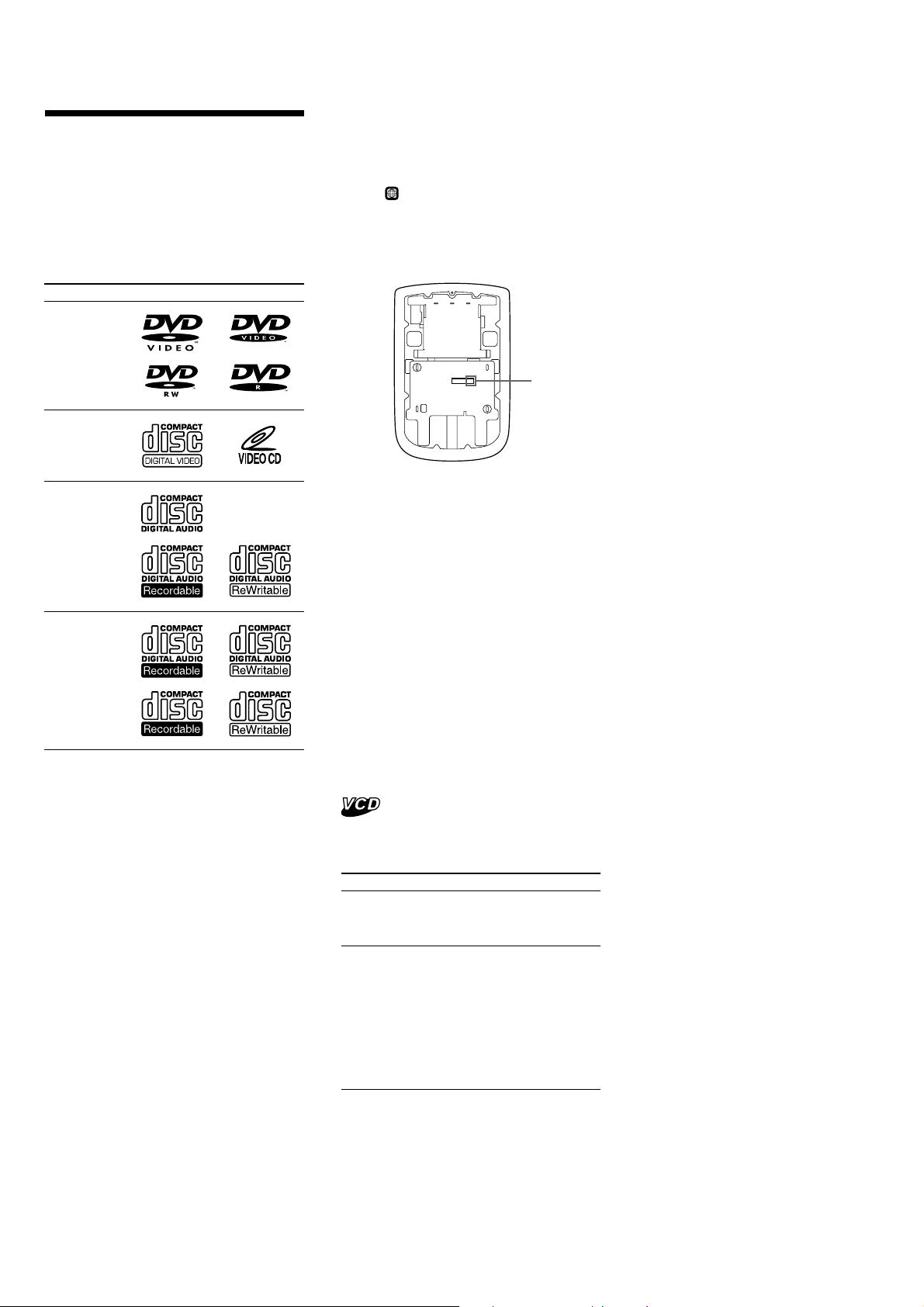
q; “Memory Stick” slot
qa x (stop) button
qs u (play/pause) button
qd OPEN button
Slide to open the monitor.
qf Speakers (left/right)
qg REVERSE button
To switch images upside down and
reverse the output of the audio channels.
qh MENU button
To make various display settings and FM
transmitter setting.
Note
Even when the player is turned off by pressing
(POWER), you can eject a disc from the player,
though you cannot insert a disc.
5
Page 6
MV-900SDS
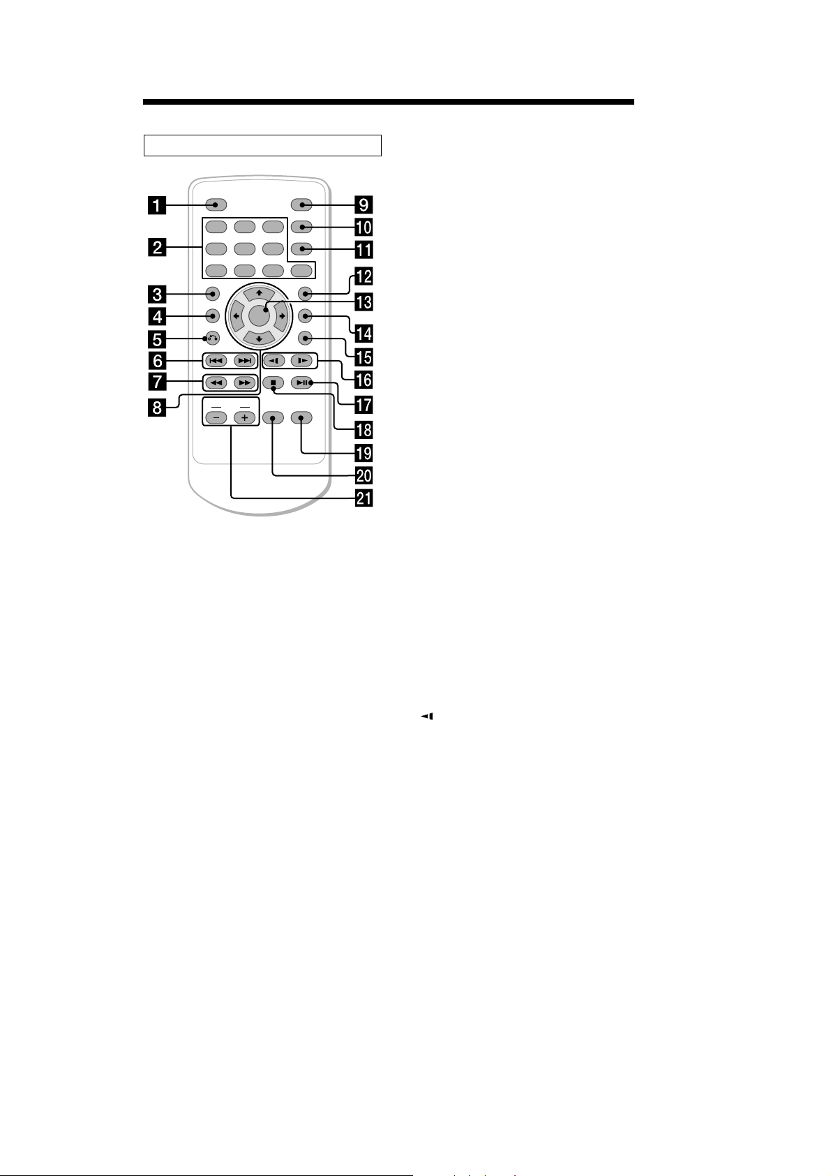
Card remote commander RM-X137
ENTER
INPUT
POWER
SEARCH
CLEAR
SUBTITLE
ANGLE
AUDIO
SETUP
DISPLAY
123
456
7 890
TOP MENU
MENU
VOL
The corresponding buttons of the card
remote commander control the same
functions as those on the player.
Instructions in this manual describe how to use
the player by mainly using the card remote
commander.
Tip
Refer to “Replacing the lithium battery” for details
on how to replace the battery.
Refer to the pages listed for details.
1 DISPLAY button
To display the time information of the disc.
2 Number buttons (0 to 9)
3 TOP MENU button
To display the top menu of a recorded
DVD.
4 MENU button
To display the recorded DVD menu, or to
turn on/off the PBC (Playback control)
menu of a Video CD.
5 O (return) button
6 ./> (previous/next) buttons
7 m (fast reverse)/
M (fast forward) buttons
8 M/,/m/< buttons
9 POWER (on/off) button
To turn on/off the player.
q; SEARCH button
To specify a desired point on a disc by
chapter, title, or track.
qa CLEAR button
qs SUBTITLE button
To change the subtitle language while
playing a DVD.
qd ENTER button
To enter a setting.
qf ANGLE button
To select the multiple angles of view while
playing a DVD.
qg AUDIO button
To change the audio output/audio
language.
qh
(slow reverse)/y (slow forward)
buttons
qj u (play/pause) button
qk x (stop) button
ql SETUP button
Used to perform menu operations.
w; INPUT button
To select the input source.
wa VOL (–/+) buttons
To turn up or down the volume.
6
Page 7
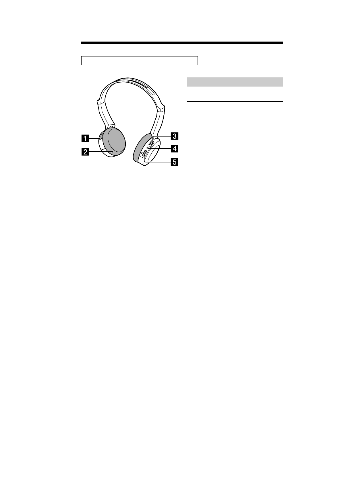
Cordless Stereo Headphones MDR-IF0140
EN
P
O
1 Battery compartment lid
To set a battery, open the lid.
2 Ear pad
The ear pads are replaceable.
3 Power (ON/OFF) switch
4 POWER indicator
When the power switch of the headphones
is set to ON, the POWER indicator lights
up in red.
5 VOL control dial
To adjust the volume level from 0 to 10.
ON
O
F
F
POW
ER
VO
L
Battery life
Size AAA dry battery (1) is supplied with the
headphones.
Battery Approx. hours*
Sony alkaline battery 60 hours*
LR03/AM-4 (N)
Sony manganese battery 28 hours*
R03/UM-4 (NU)
*1at 1 kHz, 1 mW+1 mW output
2
Time stated above may vary, depending on the
*
temperature or conditions of use.
Tip
Refer to “Replacing the battery” for details on
how to replace the battery.
2
2
MV-900SDS
1
7
Page 8
MV-900SDS
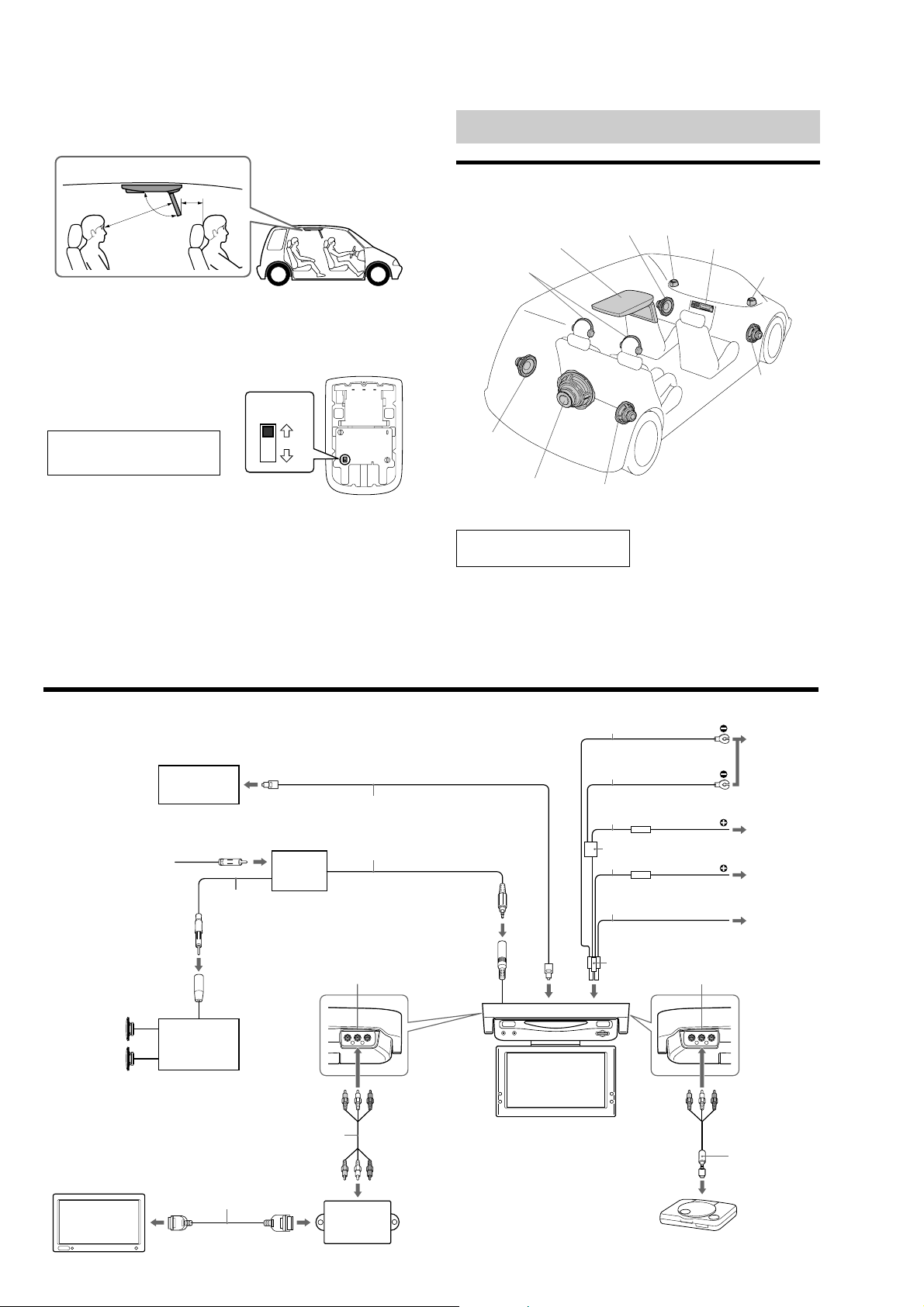
Where to install
Before installing this unit, please check your local traffic rules and regulations. Follow the diagram
below to install this unit in a suitable position in your car.
Connections
Installation diagram
Refer to the installation diagram and ask a qualified technician for the installation of the unit.
Front Left
speaker
Tweeter Left
Head unit
Tweeter Right
Cordless Stereo
Headphones
MDR-IF0140
DVD player
XVM-R90D
Do not install this unit where:
— It will obstruct the driver’s view when the
monitor is in either the open or closed
position.
— It will obstruct the operation of the airbag
system.
— It will obstruct the operation of the
vehicle, especially the steering wheel, shift
lever, or brake pedal.
—A driver or passengers may injure
themselves when getting into or out of the
car.
If you have any questions or problems
concerning your unit that are not covered
in this manual, please consult your
nearest Sony dealer.
Before installing
Make sure that the POWER SELECT switch is
set to the correct position.
A*: If your car has an accessory position on
the ignition key.
B : If your car has no accessory position on
the ignition key.
* A is the factory preset position.
When the POWER SELECT switch is
set to B
Press (POWER) on the player to turn on.
The player does not turn on by pressing
(POWER) on the card remote commander.
Note
Be sure to turn off the player after driving your
car.
To turn off the player, follow the operations
below:
– Press (POWER) on the player.
– Press (POWER) on the card remote commander.
If the power is left on, it will cause battery drain.
Connection diagram
Refer to the connection diagram for the proper connections.
Note
Set the POWER SELECT switch before installing (page 6).
Amplifier equipped
with a digital input
(optional)
From the car antenna
0.5 m
POWER SELECT
switch
Relay box
Front Right
speaker
B
A
Optical cable
(optional)
5 m
Rear Left
speaker
Subwoofer
Be sure to securely fasten all equipment to
the car chassis, etc., to prevent them
moving while your car is in motion.
Note
All equipment other than one DVD player and two
cordless stereo headphones is optional.
Rear Right
speaker
Black
Black
Yellow
Filter box
Red
Blue
Notes on the locations for PS one™
Do not set PS one™:
— on a dashboard, or in a place subject to direct
sunlight.
— in a place near magnetic source such as
magnets, speakers and a TV/Monitor.
— on an unstable or uneven surface.
— in a place subject to excessive vibration.
— in a place subject to excessive dust or dirt.
— in poorly ventilated or humid place.
— in a place to subject to temperature extremes
(below 5˚C (41˚F) or above 35˚C (95˚F)).
Refer to the operating instructions supplied to PS
one™.
“PS one” is a trademark of Sony Computer
Entertainment Inc.
GND (1 m)
GND (1 m)
Back-up (5 m)
Fuse (5 A)
Fuse (1 A)
ACC (5 m)
POWER REM (5 m)
Max. supply current 0.3 A
To a metal surface
of the car chassis
To car battery
(12 V)
To ignition switch*
(ACC position)
To a power
amplifier
2
Antenna connector*
Speaker system
(optional)
1
*
An adapter (optional) may be necessary for your
car and car audio system. In such a case, consult
your dealer.
2
If your car has no ACC (accessory) position on
*
the ignition key switch, set the POWER SELECT
switch to B (page 6) and connect this ACC cable
to the +12 V power (battery) terminal.
Monitor (optional)
Car audio
(optional)
8
1
Monitor cable (optional)
AUDIO/VIDEO OUTPUT
RCA pin cord (optional)
Connection box
(optional)
4 Pin Power connector
Precautions on PS one™
• Be sure to fasten PS one™ in a safe place
securely.
• For your safety, do not use PS one™ while
driving your car.
• Make sure that the operating voltage of PS
one™ is 7.5 V. Other voltages may cause
malfunction, or damage PS one™.
Refer to the operating instructions supplied to
PS one™.
“PS one” is a trademark of Sony Computer
Entertainment Inc.
AUDIO/VIDEO INPUT
PS one™ (optional)
AV Cable
(integrated audio/video)
(optional)
Page 9
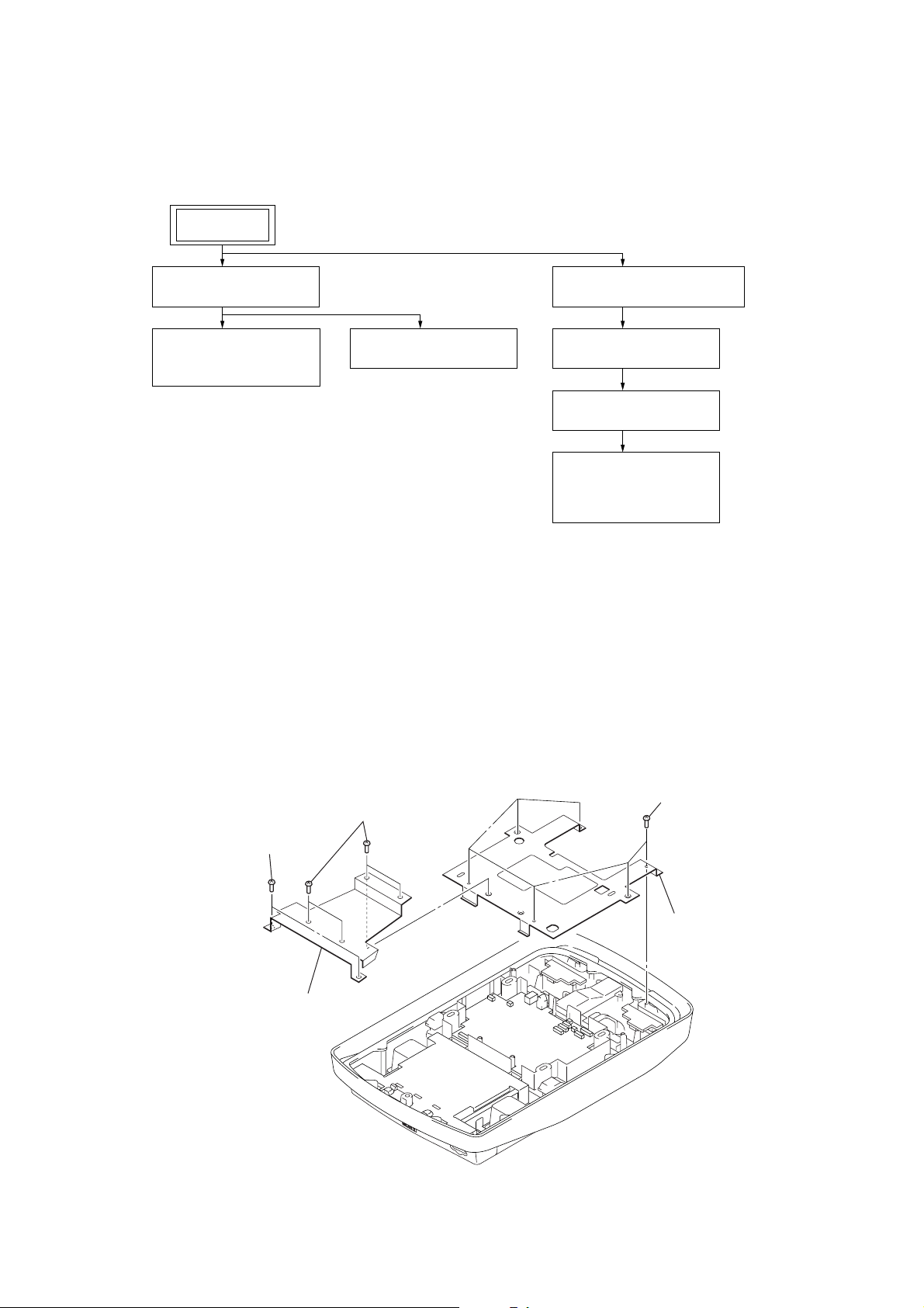
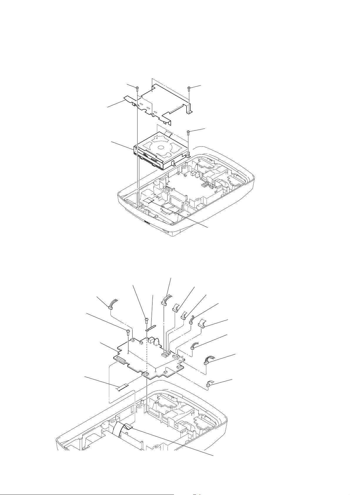
• This set can be disassembled in the order shown below.
)
3-1. DISASSEMBLY FLOW
SET
MV-900SDS
SECTION 3
DISASSEMBLY
3-2. BRACKET (MAIN)
(Page 9)
3-3. DVD MECHANISM
DECK BLOCK
(Page 10)
Note: Follow the disassembly procedure in the numerical order given.
3-4. MAIN BOARD
(Page 10)
3-2. BRACKET (MAIN)
3-5. REAR COVER (HINGE)
(Page 11)
3-6. LCD BLOCK
(Page 11)
3-7. LCD BOARD
(Page 12)
3-8. LIQUID CRYSTAL
DISPLAY PANEL
(LCD1)
(Page 12)
2
two screws
(BTP2.6
3
1
four screws
(B2.6
×
8)
bracket (support)
4
six screws
(BTP2.6
×
4)
×
8)
5
bracket (main
9
Page 10
MV-900SDS
3-3. DVD MECHANISM DECK BLOCK
2
two screws
4
bracket (front)
6
(BTP2.6
DVD mechanism
deck block
×
6)
3
two screws
(BTP2.6
5
two screws
(BTP2.6
×
8)
×
8)
3-4. MAIN BOARD
3
three screws
(BTP2.6
1
flexible flat cable
(30P) (CN102)
2
connector (CN702)
×
8)
5
MAIN board
3
screw
(BTP2.6
1
flexible flat cable
(50P) (CN101)
2
connector (CN108)
×
8)
4
harness
2
connector (CN105)
2
connector (CN107)
2
connector (CN302)
2
connector (CN103)
2
connector (CN104)
2
connector (CN701)
2
connector (CN705)
10
1
flexible flat cable
(50P) (CN101)
Page 11
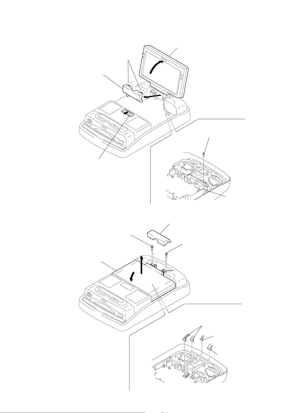
3-5. REAR COVER (HINGE)
4
rear cover
(hinge)
3
two claws
A
B
LCD block
2
two screws
(P2 × 8)
MV-900SDS
1
Slide the knob (open) in the direction
of arrow A, and open the LCD block
in the direction of arrow B.
3-6. LCD BLOCK
5
4
two screws
(PS3
Lifting up the LCD block in
the direction of arrow
A
.
×
10)
1
A
3
front cover (hinge)
4
two screws
(PS3
×
rear cover
(hinge)
10)
2
two connectors
(CN105, 108)
2
connector
(CN107)
2
connector
(CN103)
11
Page 12
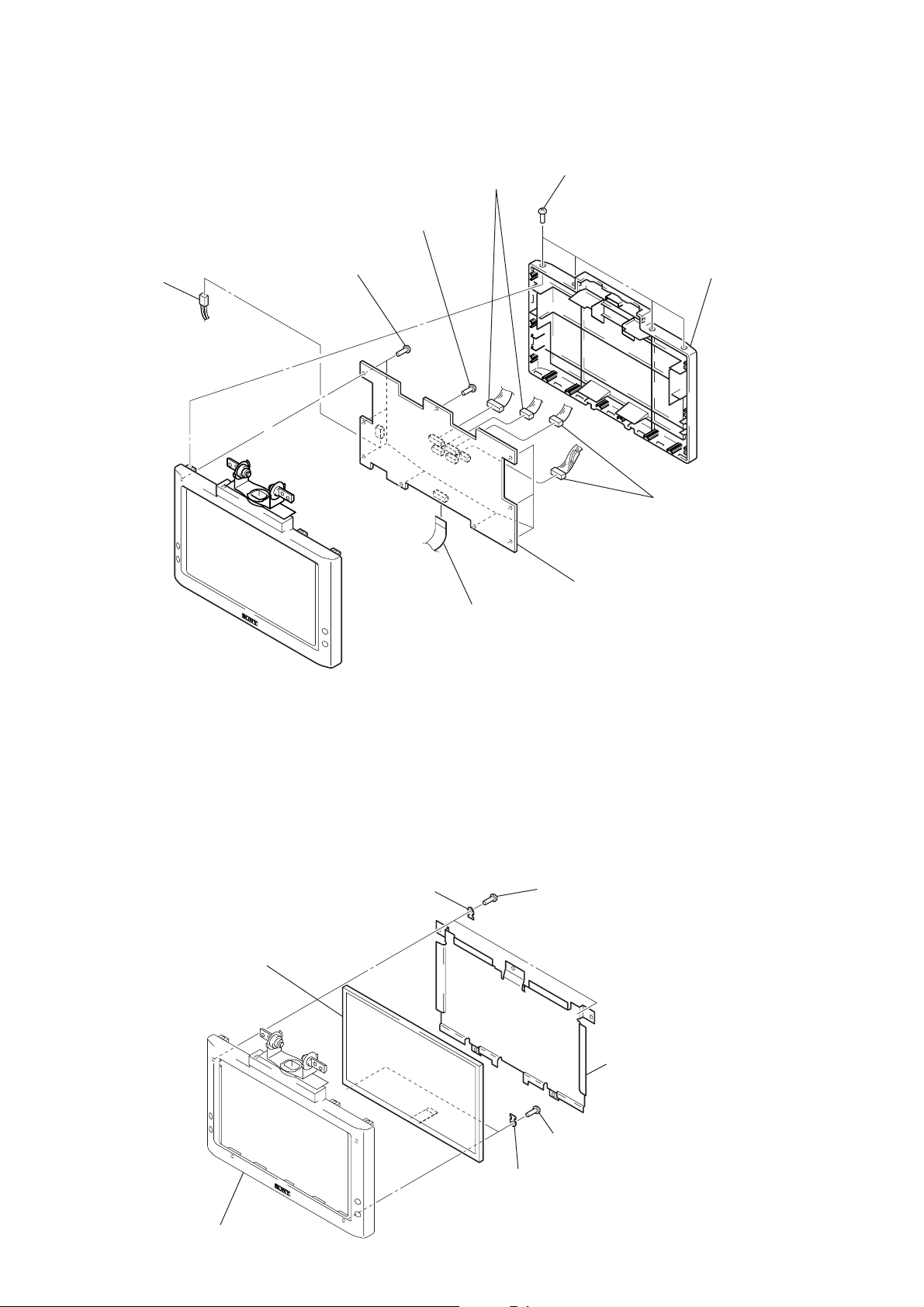
MV-900SDS
)
3-7. LCD BOARD
4
connector
(CN850)
5
eight screws
(BTP2 × 6)
6
screw
(PS2.6 × 6)
4
two connectors
(CN906, 907)
1
four screws
(B2 × 5)
2
rear case (LCD
3-8. LIQUID CRYSTAL DISPLAY PANEL (LCD1)
2
two retainers (LCD)
6
liquid crystal display panel
(LCD1)
3
flexible board
(CN801)
1
two screws
(BTP2 × 6)
7
LCD board
4
two connectors
(CN905, 908)
12
front case (LCD) block
4
5
two retainers
(LCD)
3
two screws
(BTP2 × 6)
shield plate
(LCD)
Page 13
SECTION 4
TEST MODE
MV-900SDS
Note: This set is able to setting the adjustment data, reset to factory default
and initialize the EEPROM (IC402 on the MONITOR board) in the
test mode.
ENTER THE TEST MODE
Procedure:
1. Press the [POWER] button to turn the power ON.
2. While pressing the [VOL --] and . buttons, press the
[RESET] button.
3. The set is enter the test mode and display as bellow figure.
Display
TEST MODE MENU
1. NTSC/PAL SELECT
2. FOR FACTORY
3. LCD SETTING
4. FM TRANSMITTER
5. HEAT PROTECTION
6. VOLTAGE SETUP
7. LOAD DEFAULT
8. SOFT RESET(EXIT)
Dream System 20XX
Ver.20XX-XX-XXx
Note: If initial data is not written to the EEPROM (IC402 on the MONITOR
board) or data is clobbered, the set is not able to display normally
screen.
BATCH WRITING OF THE INITIAL DATA TO
EEPROM
In the test mode, by pressing the [VOL --] button at two seconds,
batch writing is possible of the initial data to EEPOM (IC402 on
the MONITOR board).
3. LCD SETTING
This mode is not used in servicing.
4. FM TRANSMITTER
In this mode, switch the frequency range of FM transmitter as
follow.
1) USA (88.3 to 89.9 MHz)
2) Japan (76.5 to 79.5 MHz)
3) Transmitter off
5. HEAT PROTECTION
This mode is not used in servicing.
6. VOLTAGE SETUP
This mode is not used in servicing.
7. LOAD DEFAULT
This mode is not used in servicing.
8. SOFT RESET (EXIT)
Releasing the test mode.
OPERATION OF THE TEST MODE
All operations are performed using the bellow buttons.
Button Function
MENU Select the item
REVERSE Enter
VOL + Up the data value
VOL − Down the data value
RELEASING THE TEST MODE
In the test mode menu screen, press the [MENU] button to select “8.
SOFT RESET (EXIT)”, and press the [REVERSE] button to release
the test mode.
OPERATING THE EACH ITEM
1. NTSC/PAL SELECT
In this mode, switch the signal format system to NTSC or P AL.
2. FOR FACTORY
In this mode, change the data of adjustment data.
Enter this mode, it displays each adjustment item as follow.
1) Com Gain
2) Y Gain
3) Black Limit
4) White Limit
5) R-Sub BRT
6) B-Sub BRT
7) R-Sub CONT
8) B-Sub CONT
9) Gamma 1
10) Gamma 2
11) VCO Free Run
12) PLL/V Pos
13) H Pos
13
Page 14
MV-900SDS
r
r
r
r
r
r
SECTION 5
ELECTRICAL ADJUSTMENTS
1. DC/DC CONVERTER ADJUSTMENT
1-1. Frequency Adjustment
Setting:
oscilloscope
or
frequency counte
MONITOR board
TP802
TP804
Procedure:
1. Connect an oscilloscope or frequency counter to the TP802
and TP804 on the MONITOR board.
2. Check that the voltage between TP951 (−) and TP952 (+) is
14.4 V. Press the [POWER] button to turn the power on.
3. Adjust the RV801 on the MONITOR board so that the value
of oscilloscope or frequency counter becomes 243 kHz ±3
kHz.
1-2. 5V Voltage Adjustment
Setting:
MONITOR board
TP807
TP804
Procedure:
1. Connect a digital voltmeter to the TP804 and TP807 on the
MONITOR board.
2. Check that the voltage between TP951 (–) and TP952 (+) is
14.4 V. Press the [POWER] button to turn the power on.
3. Adjust the RV803 on the MONITOR board so that the value
of digital voltmeter becomes 5.05 V ±0.03 V .
1-3. Other Voltages Check
Setting:
MONITOR board
TP805/TP806/TP808
TP804
Procedure:
– Vdd Voltage Check –
1. Connect a digital voltmeter to the TP804 and TP808 on the
MONITOR board.
2. Check that the voltage between TP951 (–) and TP952 (+) is
14.4 V. Press the [POWER] button to turn the power on.
3. Check that the value of digital voltmeter is 3.45 V ±0.2 V.
– Vgh Voltage Check –
4. Connect the digital voltmeter to the TP804 and TP806 on the
MONITOR board.
5. Check that the value of digital voltmeter is 17.5 V ±1.5 V.
– Vss Voltage Check –
6. Connect the digital voltmeter to the TP804 and TP805 on the
MONITOR board.
7. Check that the value of digital voltmeter is –12.0 V ±1.5 V.
+
–
digital voltmete
+
–
digital voltmete
+
–
2. PLL ADJUSTMENT
Setting:
digital voltmete
MONITOR board
TP601
TP602
+
–
Procedure:
1. Connect a digital voltmeter to the TP601 and TP602 on the
MONITOR board.
2. Check that the voltage between TP951 (–) and TP952 (+) is
14.4 V. Press the [POWER] button to turn the power on.
3. Adjust the RV601 on the MONITOR board so that the value
of digital voltmeter becomes 2.4 V ±0.15 V .
3. INVERTER HIGH VOLTAGE CHECK
Setting:
digital voltmete
MONITOR board
TP853
TP854
+
–
Procedure:
– High Voltage Check –
1. Connect a digital voltmeter (for withstand high voltage) to the
TP853 and TP854 on the MONITOR board.
2. Check that the voltage between TP951 (–) and TP952 (+) is
14.4 V. Press the [POWER] button to turn the power on.
(DIMMER: off)
3. Check that the value of digital voltmeter is 550 V ±150 V
(rms).
– Frequency Check –
4. Connect an oscilloscope (use a probe for withstand high
voltage) to the TP853 and TP854 on the MONITOR board.
5. Check that the frequency of oscilloscope is 66 kHz ±2.5 kHz.
4. OSD DOT CLOCK CHECK
Setting:
MONITOR board
TP403
TP405
Procedure:
1. Connect a frequency counter (high impedance) to the TP403
and TP405 on the MONITOR board.
2. Check that the voltage between TP951 (–) and TP952 (+) is
14.4 V. Press the [POWER] button to turn the power on.
3. Check that the value of frequency counter is 6.5 MHz ±0.2
MHz.
frequency counte
+
–
14
Page 15
MV-900SDS
r
r
e
V
V
e
5. NTSC SUB CARRIER CHECK
Setting:
frequency counte
MONITOR board
TP510
TP513
+
–
Procedure:
1. Connect a frequency counter (high impedance) to the TP510
and TP513 on the MONITOR board.
2. Check that the voltage between TP951 (–) and TP952 (+) is
14.4 V. Press the [POWER] button to turn the power on.
3. In the normal mode, press the [INPUT] key on the remote
commander to select the “VIDEO” mode.
4. Input NTSC video signal to the “VIDEO INPUT” jack (J701
on the VIDEO (IN) board).
5. Check that the value of frequency counter is 3.579545 MHz
±100 Hz.
6. PAL SUB CARRIER CHECK
Setting:
frequency counte
MONITOR board
TP510
TP513
+
–
– Waveform Position Set-up Adjustment –
7. Adjust the RV802 on the MONITOR board so that A value
of waveform becomes –1.7 V ±0.1 V.
4.6 V ± 0.1 V
0 V
A
: – 1.7 V ± 0.1
8. VIDEO ADJUSTMENT
Note: Perform the following adjustment items in test mode.
Common Setting:
1. Check that the voltage between TP951 (–) and TP952 (+) is
14.4 V. Press the [POWER] button to turn the power on.
2. Enter the test mode, and enter the “2. FOR FA CTOR Y” mode.
(refer to “4. TEST MODE”)
3. Set the signal format system to NTSC. (refer to “4. TEST
MODE”)
4. Input 10 steps signal (NTSC, without burst) to the VIDEO
INPUT jack (J301 on the POWER board) from pattern
generator.
Waveform of input signal
1 Vp-p
Procedure:
1. Connect a frequency counter (high impedance) to the TP510
and TP513 on the MONITOR board.
2. Check that the voltage between TP951 (–) and TP952 (+) is
14.4 V. Press the [POWER] button to turn the power on.
3. In the normal mode, press the [INPUT] key on the remote
commander to select the “VIDEO” mode.
4. Input PAL video signal to the “VIDEO INPUT” jack (J701 on
the VIDEO (IN) board).
5. Check that the value of frequency counter is 4.433619 MHz
±100 Hz.
7. V-COM ADJUSTMENT
Setting:
oscilloscop
MONITOR board
TP819
TP832
Procedure:
– Voltage Set-up Adjustment –
1. Connect an oscilloscope to the TP819 and TP832 on the
MONITOR board.
2. Check that the voltage between TP951 (–) and TP952 (+) is
14.4 V. Press the [POWER] button to turn the power on.
3. Enter the test mode, and enter the “2. FOR FA CTOR Y” mode.
(refer to “4. TEST MODE”)
4. Press the [MENU] button to display “Com Gain”, and press
the [REVERSE] button.
5. Adjust by pressing the [+]/ – buttons so that the voltage of
oscilloscope becomes 6.3 Vp-p ±0.1 V.
+
–
0.286 V
fig. 8-1
Waveform of output signal
(TP810, TP811, TP812)
0 V
AB CDE
fig. 8-2
1 Contrast Level of Luminance Signal
Setting:
oscilloscop
MONITOR board
TP811
TP513
+
–
Procedure:
1. Connect an oscilloscope to the TP513 and TP811 on the
MONITOR board.
2. Press the [MENU] button to display “Y Gain”, and press the
[REVERSE] button.
3. Adjust by pressing the [+]/ – buttons so that the D value of
waveform (fig. 8-2) becomes 3.4 V V.
+0.2
–0.1
4. Press the [REVERSE] button and write the date to EEPROM
(IC402 on the MONITOR board).
6.3 Vp-p ± 0.1
6. Press the [REVERSE] button and write the date to EEPROM
(IC402 on the MONITOR board).
15
Page 16
MV-900SDS
r
2 Back Limiter Level
Procedure:
1. In the “1 Contrast Level of Luminance Signal” status, press
the [MENU] utton to display “Black Limit”, and press the
[REVERSE] button.
2. Adjust by pressing the [+]/ – buttons so that the A value of
waveform (fig. 8-2) becomes 1.0 V V.
+0.2
–0.1
3. Press the [REVERSE] button and write the date to EEPROM
(IC402 on the MONITOR board).
3 White Limiter Level
Procedure:
1. In the “2 Black Limiter Level” status, press the [MENU] button
to display “White Limit”, and press the [REVERSE] button.
2. Adjust by pressing the [+]/ – buttons so that the E value of
waveform (fig. 8-2) becomes 3.9 V V.
+0.2
–0.1
3. Press the [REVERSE] button and write the date to EEPROM
(IC402 on the MONITOR board).
4 R-sub Bright
Procedure:
1. In the “3 White Limiter Level” status, connect the
oscilloscope to the TP513 and TP810 on the MONITOR board.
2. Press the [MENU] button to display “R-Sub BRT”, and press
the [REVERSE] button.
3. Adjust by pressing the [+]/ – buttons so that the A value of
waveform (fig. 8-2) becomes 1.0 V V.
+0.2
–0.1
4. Press the [REVERSE] button and write the date to EEPROM
(IC402 on the MONITOR board).
5 B-sub Bright
Procedure:
1. In the “4 R-sub Bright” status, connect the oscilloscope to
the TP513 and TP812 on the MONITOR board.
2. Press the [MENU] button to display “B-Sub BRT”, and press
the [REVERSE] button.
3. Adjust by pressing the [+]/ – buttons so that the A value of
waveform (fig. 8-2) becomes 1.0 V V.
+0.2
–0.1
4. Press the [REVERSE] button and write the date to EEPROM
(IC402 on the MONITOR board).
6 R-ch Sub Contrast
Procedure:
1. In the “5 B-sub Bright” status, connect the oscilloscope to
the TP513 and TP810 on the MONITOR board.
2. Press the [MENU] button to display “R-Sub CONT”, and press
the [REVERSE] button.
3. Adjust by pressing the [+]/ – buttons so that the D value of
waveform (fig. 8-2) becomes 3.4 V V.
+0.2
–0.1
4. Press the [REVERSE] button and write the date to EEPROM
(IC402 on the MONITOR board).
7 B-ch Sub Contrast
Procedure:
1. In the “6 R-ch Sub Contrast” status, connect the oscilloscope
to the TP513 and TP812 on the MONITOR board.
2. Press the [MENU] button to display “B-Sub CONT”, and press
the [REVERSE] button.
3. Adjust by pressing the [+]/ – buttons so that the D value of
waveform (fig. 8-2) becomes 3.4 V V.
+0.2
–0.1
4. Press the [REVERSE] button and write the date to EEPROM
(IC402 on the MONITOR board).
8 Gamma 1
Procedure:
1. In the “7 B-ch Sub Contrast” status, connect the oscilloscope
to the TP513 and TP811 on the MONITOR board.
2. Press the [MENU] button to display “Gamma 1”, and press the
[REVERSE] button.
3. Adjust by pressing the [+]/ – buttons so that the B value of
waveform (fig. 8-2) becomes 1.9 V V.
+0.2
–0.1
4. Press the [REVERSE] button and write the date to EEPROM
(IC402 on the MONITOR board).
9 Gamma 2
Procedure:
1. In the “8 Gamma 1” status, press the [MENU] button to display
“Gamma 2”, and press the [REVERSE] button.
2. Adjust by pressing the [+]/ – buttons so that the C value of
waveform (fig. 8-2) becomes 3.1 V V.
+0.2
–0.1
3. Press the [REVERSE] button and write the date to EEPROM
(IC402 on the MONITOR board).
q; VCO Free Run
Setting:
frequency counte
MONITOR board
TP506
TP513
+
–
Procedure:
1. In the “9 Gamma 2” status, connect a frequency counter to
the TP506 and TP513 on the MONITOR board.
2. Press the [MENU] button to display “VCO Free Run”, and press
the [REVERSE] button.
3. Adjust by pressing the [+]/ – buttons so that the value of
frequency counter becomes 15.734 kHz ±50 Hz.
4. Confirm that the displayed screen is normally display.
5. Press the [REVERSE] button and write the date to EEPROM
(IC402 on the MONITOR board).
qa Vertical Position
Procedure:
1. In the “q; VCO Free Run” status, input the monoscope signal
to the VIDEO INPUT jack (J301 on the POWER board).
2. Press the [MENU] button to display “PLL/V Pos”, and press
the [REVERSE] button.
3. Adjust by pressing the [+]/ – buttons so that the vertical position
of screen on the monitor becomes the most suitable.
4. Press the [REVERSE] button and write the date to EEPROM
(IC402 on the MONITOR board).
qs Horizontal Position
Procedure:
1. In the “qa Vertical Position” status, press the [MENU] button
to display “H Pos”, and press the [REVERSE] button.
2. Adjust by pressing the [+]/ – buttons so that the horizontal
position of screen on the monitor becomes the most suitable.
3. Press the [REVERSE] button and write the date to EEPROM
(IC402 on the MONITOR board).
16
Page 17
Adjustment Location:
– LCD BOARD (Side A) –
RV601
RV802
MV-900SDS
TP853
RV803
RV801
– LCD BOARD (Side B) –
TP506
TP510
TP513
TP405
TP403
TP832
TP601
TP987
TP811
TP812
TP602
TP983
TP805
TP951 (
TP810
TP819
TP808
−
)
TP828
TP806
TP807
TP804
TP952 (+)
TP802
TP854
17
Page 18

MV-900SDS
MEMO
18
Page 19
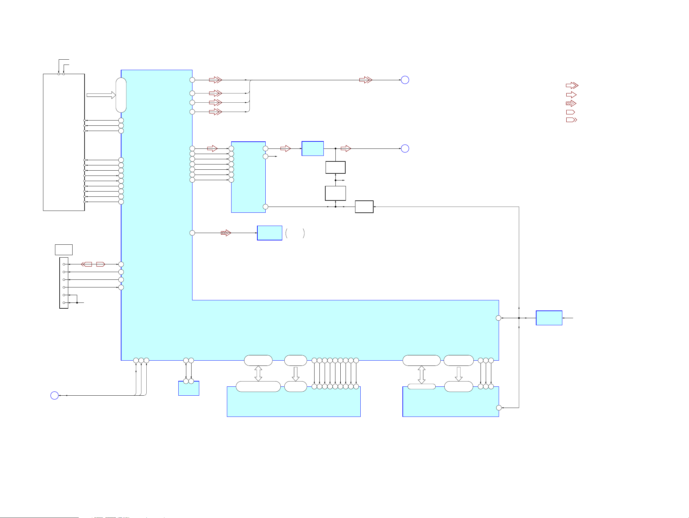
SECTION 6
DIAGRAMS
6-1. BLOCK DIAGRAM – MPEG DECODER Section –
B+8V
B+5V
+8V
+5V
HD0 – HD15
DVD MECHANISM
DECK BLOCK
HCS1J
HCS16J
HCS3J
HINTJ
IORDY
ENDSW
HA0
HA1
HA2
IOWJ
IORJ
RST
HDO – HD15
122 – 128,
131 – 137, 140, 141
154
HA0
155
HA1
158
HA2
152
XHCS1FX
151
XHIOCS16
153
HCS3FX
144
HIRQ
146
HIORDY
149
XHWR
150
XHRD
166
ENDSW
145
XHRST
114VBS
113Y
108B-Y
106R-Y
33DAC DATA
39DAC MCLK
40DAC BCK
32DAC LRCK
165DAC ML
143DAC MC
118DAC MD
CVBS
B-Y
R-Y
D/A CONVERTER
2 DATA
16 SCK
1 BCK
3 LRCK
15 ML
14 MC
13 MD
MV-900SDS
CVBS,
Y, B-Y, R-Y
Y
IC7
7VOUTL
8VOUTR
R-CH
11ZEROR
LOW-PASS
FILTER
IC701
MUTING
Q702, 704
MUTING
SWITCH
Q1, 2
R-CH
DELAY
D13, Q3
L-CH_AU
A
B
(Page 21)
(Page 20)
• R-ch is omitted due to same as L-ch.
• SIGNAL PATH
: DVD (VIDEO)
: DVD (AUDIO)
: DIGITAL OUT
: CHECK IN
: CHECK OUT
MS SDIO
MC SCLK
MS BS
MS INS
VCC
VCC
(Page 20)
MEMORY
STICK
DA-BE, CK-BE,
CS-BE
C
B+3.6V
142 MS SDIO
117 MC SCLK
167 M S BS
119 M S INS
DA-BE
DA-BE
CK-BE
CK-BE
168169162
CS-BE
CS-BE
41SPDIF
SDA
160
161
5
4
SDA
EEPROM
IC5
SCL
SCL
OPTICAL
TRANSCEIVER
J301
DB0 - DB15 DMA0 - DMA11 LD0 - LD14 LA0 - LA19
77 - 82, 85 - 90,
93 - 96
2, 4, 5, 7, 8, 10, 11, 13, 42,
44, 45, 47, 48, 50, 51, 53
DQ0 - DQ15 A0 - A11
OPTICAL
OUTPUT
MPEG DECODER
53 - 58,
61 - 66
22 - 26,
29 - 25, 22
SD-RAM
IC6
IC1
102
38
DSCK_EN
DSCK
70
CLK37CKE
DBANK0
73
20
BA021BA1
DBANK1
74
XDCAS72XDRAS0
69
18
17
XCAS
XRAS0
71
16
XDWE
100
19
XWE
XDCS0
DQM
101
39
XCS
DQMH
178 - 182, 185 - 191,
194 - 196
29 - 36, 38 - 44
DQ0 - DQ14
204 - 207, 2-7,
10 - 16, 19 - 21
45, 25, 24 - 16,
8 - 1, 48
A–1, A0 - A18
FLASH ROM
IC3
XLWRLL
198
11
XWE
176
26
XLCS3
170
28
XCE
XLOE
XOE
24XRESET
12XRST
RESET SIGNAL
GENERATOR
IC2
B+5V
MV-900SDS
1919
Page 20
MV-900SDS
6-2. BLOCK DIAGRAM – AUDIO Section –
RV900
VCO
AUDIO
INPUT
B
(Page 19)
D
(Page 21)
L-CH_AU
SW1
J701 (1/2)
L
R
R-CH
DIFFERENTIAL
AMP
IC703
AUDIO INPUT
VIN1
1
3 VIN2
SELECT
IC704
2
VOUT
SW1
7
R-CH
IR TRANSMITTER
MODULATOR
IC904
ELECTRICAL VOLUME
IC706
8
LIN1
LOUT1
CLK4DATA
5
CLK
DATA
LED DRIVE
Q902
D912, 914, 916
(IR TRANSMITTER)
• R-ch is omitted due to same as L-ch.
• SIGNAL PATH
: DVD (AUDIO)
: AUX INPUT (AUDIO)
LINE AMP
IC708
POWER ON
MUTING
Q321, 322
MUTING
Q708
MUTING
SWITCH
Q318
POWER ON
MUTING
Q319, 320
D911, 913, 915
(IR TRANSMITTER)
MUTING
B+8V
R-CH
MUTING
CONTROL
Q316, 317
Q713
R-CH
DISCHARGE SWITCH
POWER AMP
IC707
STANDBY
SWITCH
Q710, 711
+
Q714, 715
R-CH
R-CH
J702 (1/2)
POWER ON
L
R
SP1
(L)
SP2
(R)
E
AUDIO
OUTPUT
R-CH
7
(Page 22)
C
(Page 19)
DA-BE, CK-BE,
CS-BE
DA-BE
15
16
DA (IN)-BE
CK-BE
CS-BE
17
CK-BE18CS-BE
DA (OUT)-BE
DATA
7
S-SDA
CLK
6
S-SCL
BUFFER
Q206
49
Q207
FM1
R-CH
Q202, 204
RF LEVEL
SWITCHING
Q204
BUFFER
Q205
50
FM2
Q202
R-CH
22
R-CH
B+8V
1
B+ SWITCH
Q323, 324
D317
SYSTEM CONTROLLER
IC401 (1/3)
LIN
RIN
14 13
MPX ADJ
XIN
X201
7.6MHz
5
XOUT
+5V
REGULATOR
IC304
LOW-PASS FILTER
Q208, 209
FM STEREO
MODULATOR
IC201
FM+5V
VTIN
9
PD
7
17
LEVEL SHIFT
Q210 – 213
4
RF OUT
DATA16CLK15CE18ATT
3
5
FM-CE
FM-CLK
FM-DATA
64
AMP ON
BPF
FL201
(FM MODULATOR)
D204
11
53
AMUTE
MV-900SDS
2020
Page 21
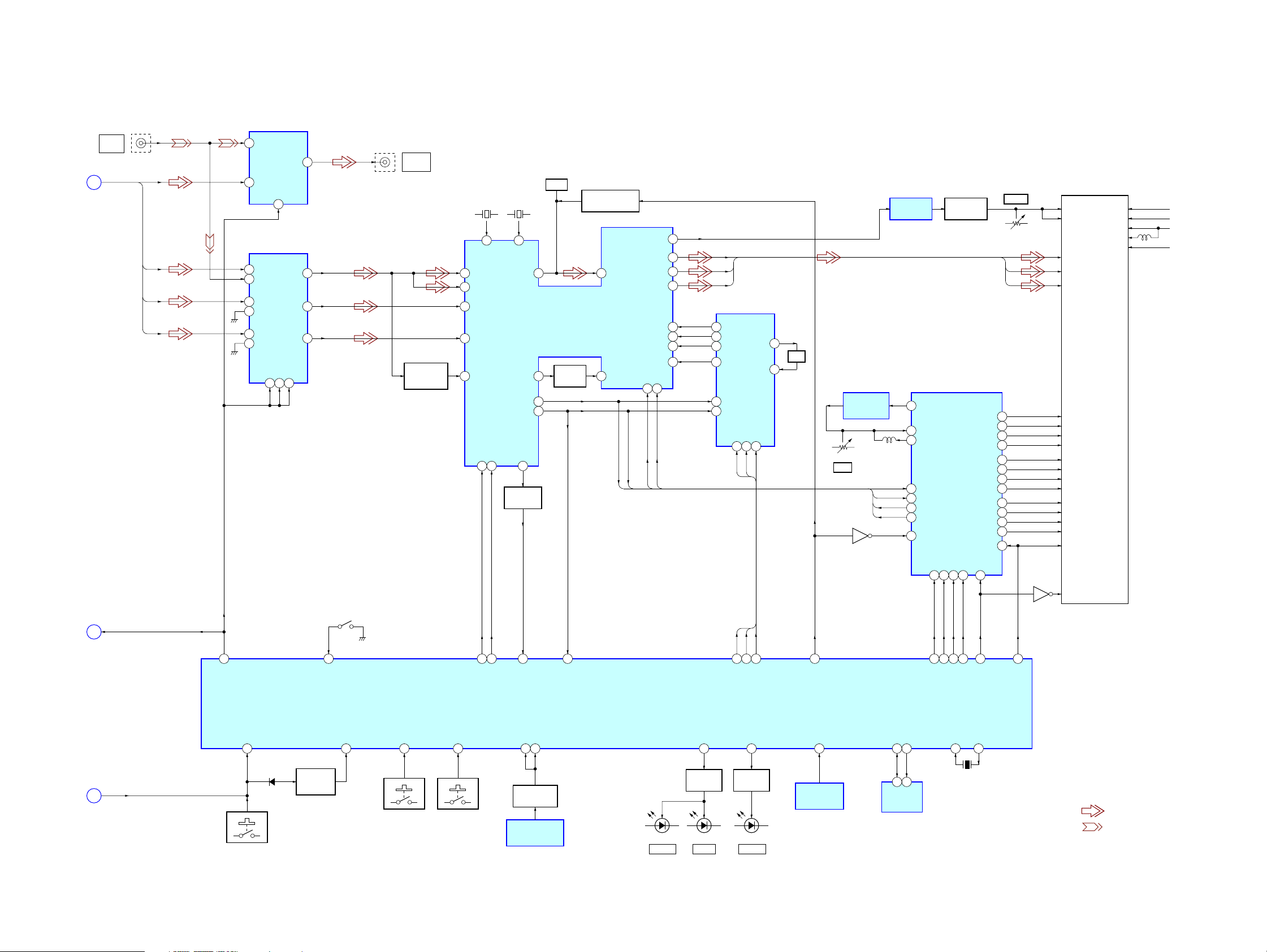
6-3. BLOCK DIAGRAM – VIDEO, PANEL Section –
VIDEO INPUT
SELECT
IC101
6 VIN1
4 VIN2
SW1
1
VIDEO INPUT SELECT
IC102
1 IN1B
16 IN1A
9 IN3B
8 IN3A
14 IN2B
11 IN2A
SW27SW3
SW1
12
2
2VOUT
3OUT1
6OUT3
5OUT2
S908
(PANEL CLOSE DETECT)
(ON: CLOSE)
30
MONITOR SW
VIDEO
INPUT
A
(Page 19)
D
(Page 20)
CVBS, Y,
B-Y, R-Y
SW1
J701 (2/2)
CVBS
Y
B-Y
R-Y
63
SW1
J702 (2/2)
VIDEO
OUTPUT
SYNC
SEPARATOR
Q502, 503
X501
3.58MHz
VXO-NTSC63VXO-PAL
CTRAPOUT
YIN
52
CIN
57
B-Y IN
5
R-Y IN
4
CSYNCIN
46
CSYNCOUT
V-SDA48V-SCK47HSYNCLOCK
51
52
V-SCK
V-SDA
X502
4.43MHz
64
HDOUT
VDOUT
39
SYNC LOCK
Q505, 506
21
SYNC-DET
TRAP
53
RGB DECODER
34
32
31
IC501
BUFFER
Q501
43
VD
PAL/NTSC SWITCH
Q504
CTRAPIN
54
VDIN
35
HD
VD
SYSTEM CONTROLLER
IC401 (2/3)
VCOMOUT
R-OUT
G-OUT
B-OUT
R-IN2
G-IN2
B-IN2
BLAK36POL
18
BLAK
POL
MV-900SDS
LIQUID CRYSTAL
Q603
DISPLAY MODULE
LCD1
VCOM
VCOM
RED
GREEN
BLUE
STV1
STV2
STH1
STH2
CPH1
CPH2
CPH3
CPV
OEV1
OEV2
OEV3
OEH
L/R
U/D
VHG
VDD1
VCC
VEE
VGH +17V
VDD +3.3V
VCC +5V
VB
VSS –13V
RV802
54
STV1
U/D
V-COM
R
G
B
20
26STV2
23STH1
24STH2
29CPH1
27CPH2
25CPH3
16CPV
19OEV1
18OEV2
17OEV3
21OEH
28L/R
55
LR
V COM AMP
IC802
28
26
21
19
14
15
16
17
YS
R
G
B
OSD DRIVER
IC405
16
VR
17 VG
18 VB
15 BLK
20 HSYNCN
19 YSYNCN
3
DATA
DATA
19
OSC OUT
SCLK2CSN
DATA
1
CLK
CS
CS
CLK
20
22
OSD CSN
OSD SCLK
OSD DATA
7
OSC
8OSC IN
PHASE
COMPARATOR
IC602
RV601
PLL
Q601
23
N/P
HD
VD
BLAK
POL
33
36 VCO1
37 VCO0
2HSYNCIN
5VDBIN
8 BLACK
14 POL
46 NP
LCD CONTROLLER
PD
QHSEL31JUST13UD
CPHSEL
4
3
59
58
SIDE1
SIDE2
V COM BIAS
Q803 – 807
IC601
LTBOX
12
57
61
JUST
ZOOM
(Page 22)
MV-900SDS
X2
KEY PW/EJ
29
D402
RESET
F
S902, 903
WAKE UP
SWITCH
Q401, 403
KEY HALT
44
KEY IN
27
S401 – 404
KEY DVD
28
S904 – 907
REM HALT45REM IN
47
SIRCS BUFFER
Q901
REMOTE CONTROL
RECEIVER
IC902
11
LED DRIVE
Q955
POWER EJECT
D901D900
LIGHT PW/EJ
DISC_LED
12
LED DRIVE
Q953
D902
DISC IN
TEMP
33
TEMPERATURE
SENSOR
IC901
SDA13SCL
14
5
SDA
EEPROM
IC402
6
SCL
X1
41 40
X401
4.19MHz
• SIGNAL PATH
: DVD (VIDEO)
: AUX INPUT (VIDEO)
2121
Page 22
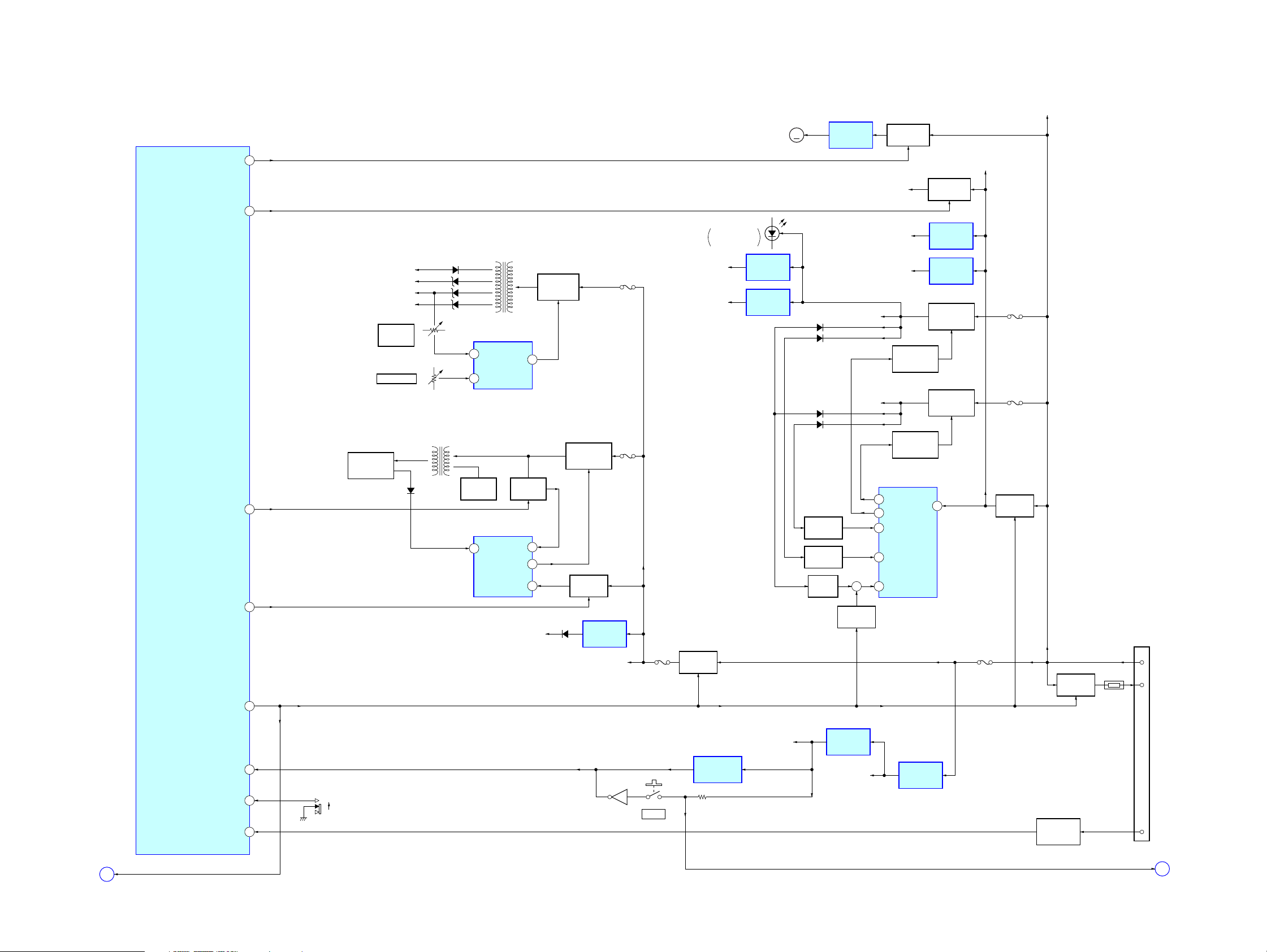
MV-900SDS
6-4. BLOCK DIAGRAM – POWER SUPPLY Section –
FAN CONT
BATT
M301
MM
(FAN)
8
+12V
REGULATOR
IC302
B+SWITCH
Q307, 308
SW12V
SYSTEM CONTROLLER
IC401 (3/3)
IR CONT
DIMMER
TFT ON
PW-ON
CONTROL
Q305, 306
CONTROL
Q302, 303
VCC
B+SWITCH
Q904, 905
+8V
REGULATOR
IC903
+8V
REGULATOR
IC303
SWITCHING
REGULATOR
Q304
SWITCHING
REGULATOR
Q301
9
F950
F302
F301
B+ SWITCH
Q309, 311
B+ SWITCH
Q325, 326
CN301
3
2
BATT
AMP REM
IR LED B+
48
D903
DC/DC
CONVERTER
VSS –13V
VGH +17V
VCC +5V
VDD +3.3V
RV803
5V
VOLTAGE
(DC/DC CONVERTER)
RV801
FREQUENCY
(DC/DC CONVERTER)
INVERTER
TRANSFORMER
BACK LIGHT
UNIT
D852, 853
60
56
2
D801
D802
D803
D804
T850
Q857, 858
T801
POWER CONTROL
IC801
3
1IN+
2RT
OSC
POWER CONTROL
IC850
1IN+
1
71OUT
DIMMER
Q860, 861
162IN+
11
C2
12VCC
VCC +7.5V
DC/DC
CONVERTER
Q801, 802
D950
SWITCHING
REGULATOR
Q855, 856, 859
B+ SWITCH
Q853, 854
+8V
REGULATOR
IC950
VCC
F801
F850
F951
B+ SWITCH
Q951, 952
DISC SLOT
ILLUMINATION
B+2.8V
B+3.6V
SWITCHING
REGULATOR
IC305
SWITCHING
REGULATOR
IC306
D305
D307, 308
D306
D315, 316
DEAD TIME
Q310
DEAD TIME
Q314
LATCH
Q313
+
SWITCHING
Q312
E-VOL +8V
B+5V
B+8V
POWER CONTROL
1
OUT1
10 OUT2
6 DT1
11 DT2
15 SCP
IR +8V
REGULATOR
REGULATOR
IC301
MV-900SDS
E
(Page 20)
POWER ON
RESET
ACC Y/N
ACC IN
U-COM +3.3V
36
Q402
31
46
B
S301
(POWER SELECT)
A
S901
RESET
RESET SIGNAL
GENERATOR
IC403
+3.3V
REGULATOR
IC952
PANEL +5V
+5V
REGULATOR
IC951
ACCESSORY
DETECT
Q315
4
RESER
ACC
F
(Page 21)
2222
Page 23
• Note for Printed Wiring Boards and Schematic Diagrams • Circuit Boards Location
MV-900SDS
Note on Printed Wiring Boards:
• X : parts extracted from the component side.
• Y : parts extracted from the conductor side.
• x : parts mounted on the conductor side.
• : Pattern from the side which enables seeing.
(The other layers' patterns are not indicated.)
Caution:
Pattern face side: Parts on the pattern face side seen from
(Conductor Side) the pattern face are indicated.
Parts face side: Parts on the parts face side seen from
(Component Side) the parts face are indicated.
Caution:
Pattern face side: Parts on the pattern face side seen from
(Side B) the pattern face are indicated.
Parts face side: Parts on the parts face side seen from
(Side A) the parts face are indicated.
Note on Schematic Diagram:
• All capacitors are in µF unless otherwise noted. (p: pF)
50 WV or less are not indicated except for electrolytics
and tantalums.
• All resistors are in Ω and 1/
specified.
• C : panel designation.
• A : B+ Line.
• B : B– Line.
• H : adjustment for repair.
• Power voltage is dc 14.4V and fed with regulated dc power
supply from ACC and BATT cords.
• Voltages and waveforms are dc with respect to ground
under no-signal conditions.
no mark : DVD PLAY
(): STANDBY
∗ : Impossible to measure
• Voltages are taken with a V OM (Input impedance 10 MΩ).
Voltage variations may be noted due to normal production tolerances.
• Waveforms are taken with a oscilloscope.
Voltage variations may be noted due to normal production tolerances.
• Circled numbers refer to waveforms.
• Signal path.
L : DVD (VIDEO)
F : DVD (AUDIO)
J : DIGITAL OUT
a : AUX INPUT (VIDEO)
E : AUX INPUT (AUDIO)
d : CHECK IN
G : CHECK OUT
4
W or less unless otherwise
JACK (OUT) board
MAIN board
JACK (IN) board
LCD board
FRONT board
SW board
SERVO board
KEY board
MV-900SDS
2323
Page 24
MV-900SDS
Ver 1.1
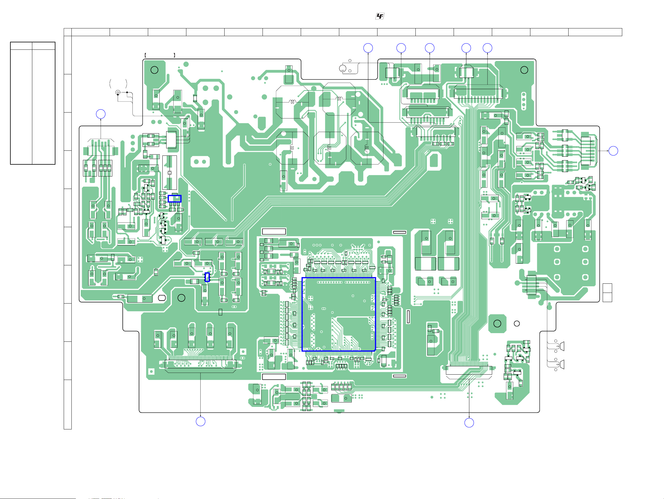
6-5. PRINTED WIRING BOARD – MAIN Board (Component Side) –
• See page 23 for Circuit Boards Location.
: Uses unleaded solder.
• Semiconductor
Location
Ref. No. Location
D4 I-9
D13 I-12
D204 D-3
D317 F-3
IC1 H-7
IC101 G-4
IC304 E-3
Q1 I-12
Q2 I-12
Q3 I-12
Q205 E-3
Q206 F-3
Q207 E-3
Q208 D-2
Q209 E-3
Q708 E-12
Q709 E-12
Q710 D-14
Q711 D-14
1 2 3 4 5 6 7 8 9 10 11 12 13 14
CN103
(Page 30)
B
C732
+
C736
+
C738
+
C735
C744
C743
LCD BOARD
CN906
113
+
+
+
R730
R754R755
+
C734
+
C718
+
C719
R731
R84
Q3
BCEQ2BCE
R86
R87
R85
R88
+
C150
R83
D13
AKA
C726
C724
C725
C727
R769
R768
+
C745
+
C340
R80
C149
R775
R774
4
1
Q709
BCE
ECB
Q708
R82
ECB
+
+
+
+
CN705
R81
R738
R740
R736
R734
L701
CN701
1
D
R784
7
R785
JACK (IN)
BOARD
CN703
(Page 37)
11
(11)
L702
R735
R737
R741
R739
+
C755
+
C756
L703
R782
+
C757
R781
R783
Q711
Q710
ECB
BCE
+
C759
1-863-445-
+
4
3
Q1
2
1
SP1
(L-CH)
–
+
SP2
(R-CH)
–
(Page 30)
LCD BOARD
CN908
11
2
3
MAIN BOARD
+
C397
A
FM
MODULATOR
ANTENNA
B
(Page 37)
JACK (OUT)
CN704
E
C
61
CN702
R1760
R1761
R1762
D
E
+
C776
+
C772
R1759
L704L705
+
C771
+
C775
R1758
C218
C211
C217
R211
R218
+
+
F
+
C769
+
G
C766
+
C765
R786
R103
C342
C343
+
+
H
I
J
C222
L203
Q208
C215
R217
C165
R214
C226
C219
R212
R216
ECB
+
R236
R235
L202
SGD
C221
R215
+
C220
D204
KA
+
R231R213
Q209
C255
Q205
A
A
+
C367
(COMPONENT SIDE)
+
CN201
3
1
X201
R227
R228
R229
13
R230
C346 C345
BCE
Q207
BCE
Q206
BCE
K
D317
C176
+
C372
150
C362
IC304
+
C344
+
C364
+
C169
L101
R105
+
C370
L307
+
C162
CN101
+
C365
+
IC101
136
+
C166
C170
+
4
C378
+
C254
+
C175
+
C161
C171
+
+
C173
R108R107
+
C168
R106R104
+
C381
C177
C178
C179
C134
C100
C95
+
C384
FB2
FB1
FB3
L1
L3
L4
C147
+
C146
+
1
M301
+
C324
L305
L302
+
C328
+
C22
C23
L51
C96
R70
R31
C31
R32
C99
R72
C34
R34
C35
RB10
RB11
C44C52C58
RB12
RB13
RB14
RB15
+
RB16
+
C144
C702
+
C705
C701
R29
R30
+
C72
L56
C30
C33
105
C32
156
C69
C66
C68
R66
R68
R712
R710
+
+
R704
R703
R709
C704
C703
R711
C710
C711
M
–
(FAN)
L303
C27C28C29
L306
2
R27
RB3RB4RB5RB6RB7RB8
R25
R24
C26
IC1
R44
R43
R42
C74
C71
R40
C103
C104
R75
R76
+
C706
+
C78
C75
C102
C101
R77
R73
R74
+
(Page 30) (Page 30)
LCD BOARD
F C
RB2
C24C25
RB21
CN905
CN302
2
L304
C21
L48
C19
RB1
53104
208157
C82
C17
52
1
D4
+
R21
R20
R19
R12
R9
R8
R7
R5
C4 C7 C18
RB20
RB19
RB18
RB17
C1 C2 C3
AK
LCD BOARD
H
CN907
+
1
C151
C105
C106
C135
C338
CN107
CN105
L314
C392
G
+
C395
+
CN108
R377
+
(Page 37)
SW BOARD
+
C335
18
111
110
R111R110R109
+
C390
L313
+
C386
C383
C382
130
CN104
12
CN102
MV-900SDS
SERVO BOARD
P
CN1
(Supplement-1
page 11)
KEY BOARD
A
CN911
(Page 36)
2424
Page 25
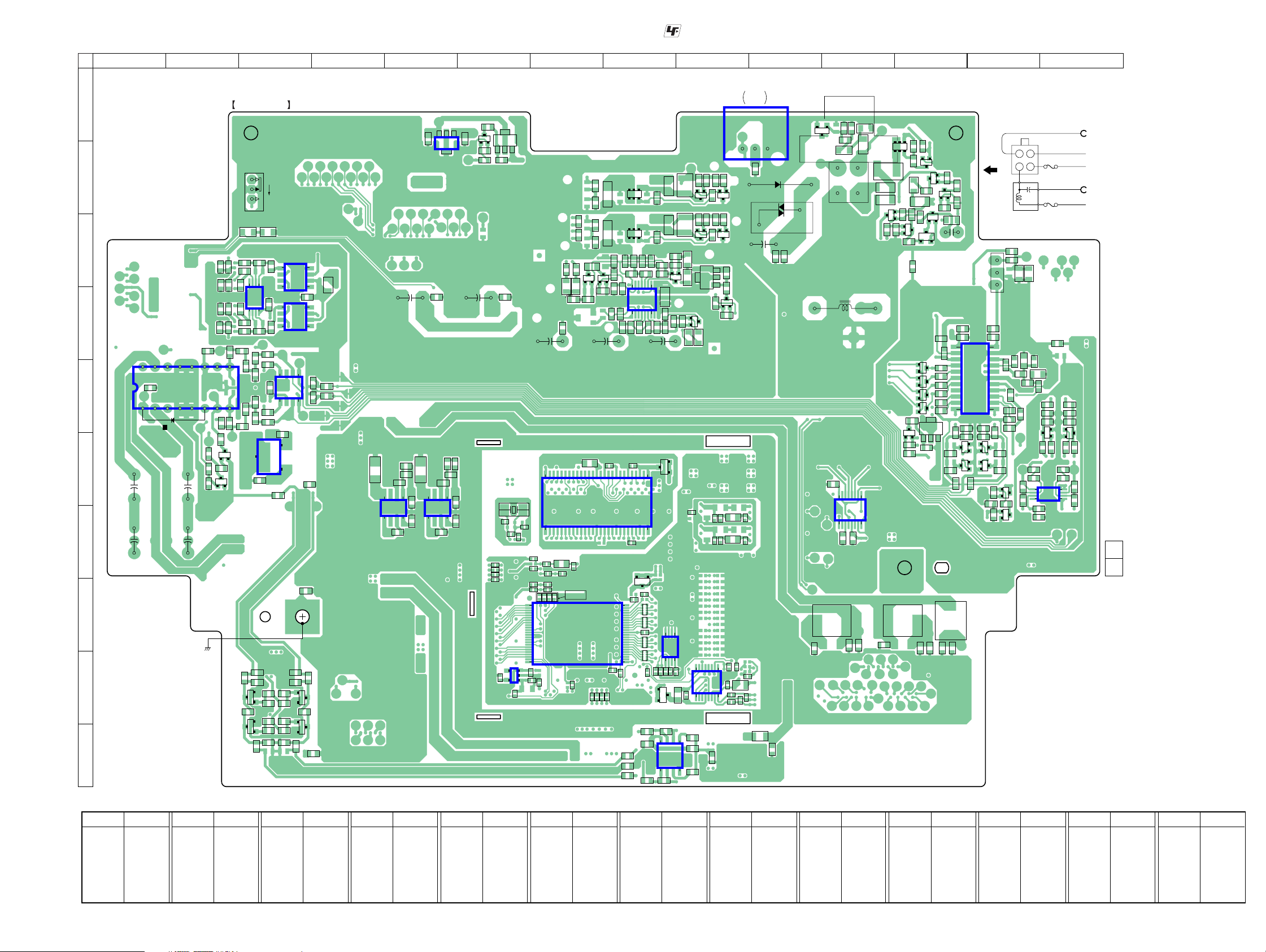
6-6. PRINTED WIRING BOARD – MAIN Board (Conductor Side) –
1 2 3 4 5 6 7 8 9 10 11 12 13 14
A
MAIN BOARD
S301
(POWER SELECT)
B
D303
AK
C
R752
R748
C720
R742
R746
4 1
C722
R744
IC703
C723
R745
R751 R750
5 8
BCE
Q714
R743
BCE
R778
C721
C751
9
C752
Q715
R1768
R777R779
R776
R747
R749
C749
C750
R753
C747
R772 R773
C748
3
C341
D
18
C758
E
F
C761
G
C763
IC707
16
D701
R1769
R1767
R1765
C762
+
R1766
+
C764
+
+
A
B
D304
KA
C733
R771
R767
R766
R770
C746
IC704
1
4
1
4
C731 C730
IC705
IC706
4
58
R761
2
IC303
1
C253
(CONDUCTOR SIDE)
8
5
L350
C737
8
5
1
R762
R764R765
R763
C796
C797
IC305
KA
R369
8 5
14
C387
R368
C391
C314
+
D321D320
KA
C389C388
H
(CHASSIS)
R719
R1709
R725
C717
R721
C715
R1710
C716
R726
C714
R722
C712C713
C790
R720
ECB
ECB
R1734
Q704
Q702
C795
C791
I
R1733
Q703
BCE
R723 R724
Q701
BCE
J
• See page 23 for Circuit Boards Location.
C
R337
13
BCE
Q308
C336
IC302
C337
Q307
R336
B
E
R338R335
R313R314R306
D314
R312R308
R305
D302
R330
R333
R334
AK
AK
C10
R1
Q313
R331R332
C92
R2R3R4
BCEBCE
R327
Q312
C304
IC6
R372
C396
R371
IC306
8
5
14
C400
R370
C394
C393
C320
C321C313
+
X1
C14
R22
L55
L11
L12
L41
D306
C310
+
C309
C15
R23
R16
R17
L52
C9
R14
R11
R10
1
C8
C6
C5
D305
IC3
24
IC2
453
C80
1
C83
R47
R46
R48
R49
AK
AK
C333R329C348
C326
R316
+
D14
R90
R57
L9L8L7
L10
R716
R727
R715
Q304
D
D
DDG
Q301
D
D
DDG
C350
R325
R326 C330
R324
IC301
C351
R315
C90C91
C94
R54
48
25
S
S
C347
R714
C707
R713
K
R321
171
127
5428
A
R52
RB25
RB24
RB23
RB22
R39
: Uses unleaded solder.
C317
R310
R309
C305 C316
R322
C331
814
Q314
C329
C327 R318
R317
R319
C315
D1
K
IC5
4
C84
58
C87
C89
R61
A
D12
C708
8
14
C709
+
F301 F302
C332
R328R323
ECB
A
K
C349
1
R62
R307
R301
D307
D308
R320
D316
C86
L53
5
IC701
Q305
C306
R302
Q302
Q309
KA
E
C
KA
B
Q310
ECB
D315
KA
KA
R33
R71
16
IC7
18
C143
R708
R706
R707
R311
R304
R705
ECBECB
Q306
R303
ECBECB
Q303
R380
C97
R69
9
BCE
R381
C157
C148
C145
J301
OPTICAL
OUTPUT
13
C318
C307
R378R379
Q311
L2
L50
C794
L54
C793
L707
C792
L706
MV-900SDS
R341
R340
AK
D310
34
CN301
1
L301
C172
IC102
C174
L311
C339
C377
D309
KA
2
18
169
C167
C376
R339
Q318
R383
C398
C369
TH301
D
R351
Q323
DD
BCE
Q325
DGS
R352
L309
D312
R355
R354
Q210
Q211
Q212
Q213
R365
BCE
R367
R364
ECB
R353
Q316
ECB
R385 R384
KA
R358
R357
R356
KAK
D318
C251
R366
C371
R386
BCE
ECB
ECB
ECB
ECB
Q324
Q326
Q319
Q317
C373
BCE
Q320
C229
R223
R224
R225
R226
C231
C232
BCE
R361
C368
R360
AK
C363
12
C230
22
R204
R206
L308
C366
R359R362
D313
C227
C228
IC201
C204
C202
R202
Q202
Q204
R208
BLK
GND
BLU
R794
R790
R1702
C774
R798
8
5
RED
BLK
YEL
R796
AMP REM
ACC
GND
BATT
Q712
ECB
R792
C768R788
TO
1
11
1
C201
R343
R344
Q321
R342R345
Q322
C225
R221
C210
C209
R210
R232
ECB
ECB
D202
C213
C214
C212
3 4
AK
C224
R209
C767R789
2
+
AK
L201
KA
Q713
R793
R791
1
4
D203
C770
R787
C223
F304
F303
D201
R219
R1701
C773
R799
BCE
R795
IC708
C252
R797
CN301
FL201
3
1
R220
C216
C203
R201
R203
Q201
ECB ECB
BCE BC E
R205
Q203
R207
11
1-863-445-
(11)
Q315
ECB
C325
D301
VDR301
C301
+
C303
C302
C98C79
C379
R78
L312
C385
• Semiconductor Location
MV-900SDS
D1 F-8
D12 I-8
D14 H-8
D201 E-14
D202 C-13
D203 C-13
D301 B-10
Ref. No. LocationRef. No. Location
D302 C-8
D303 C-3
D304 C-3
D305 D-7
D306 D-7
D307 C-9
D308 C-9
Ref. No. Location Ref. No. Location Ref. No. Location
D309 A-11
D310 B-11
D312 B-12
D313 C-12
D314 B-8
D315 D-9
D316 D-9
D318 C-12
D320 F-4
D321 F-5
D701 E-1
IC2 I-6
IC3 H-7
IC5 H-8
IC6 F-7
IC7 I-9
IC102 G-11
IC201 E-13
IC301 D-8
IC302 B-5
Ref. No. Location Ref. No. Location Ref. No. Location
IC303 F-3
IC305 F-4
IC306 F-6
IC701 J-9
IC703 D-3
IC704 C-3
IC705 D-3
IC706 E-3
IC707 E-2
IC708 F-14
J301 A-10
Q201 F-13
Q202 F-13
Q203 F-13
Q204 F-13
Q210 E-12
Q211 E-12
Q212 E-12
Q213 E-12
2525
Ref. No. Location Ref. No. Location
Q301 C-8
Q302 C-9
Q303 C-9
Q304 B-8
Q305 B-9
Q306 B-9
Q307 A-6
Q308 A-6
Q309 C-9
Q310 D-9
Q311 D-9
Q312 D-7
Q313 C-7
Q314 C-8
Ref. No. Location
Q315 A-11
Q316 C-12
Q317 C-12
Q318 C-11
Q319 B-12
Q320 B-12
Q321 F-13
Ref. No. Location Ref. No. Location
Q322 G-13
Q323 E-12
Q324 E-12
Q325 B-12
Q703 I-3
Q704 I-3
Q712 F-14
Q713 F-14
Q326 B-12
Q701 J-3
Q702 J-3
Page 26
MV-900SDS
Ver 1.1
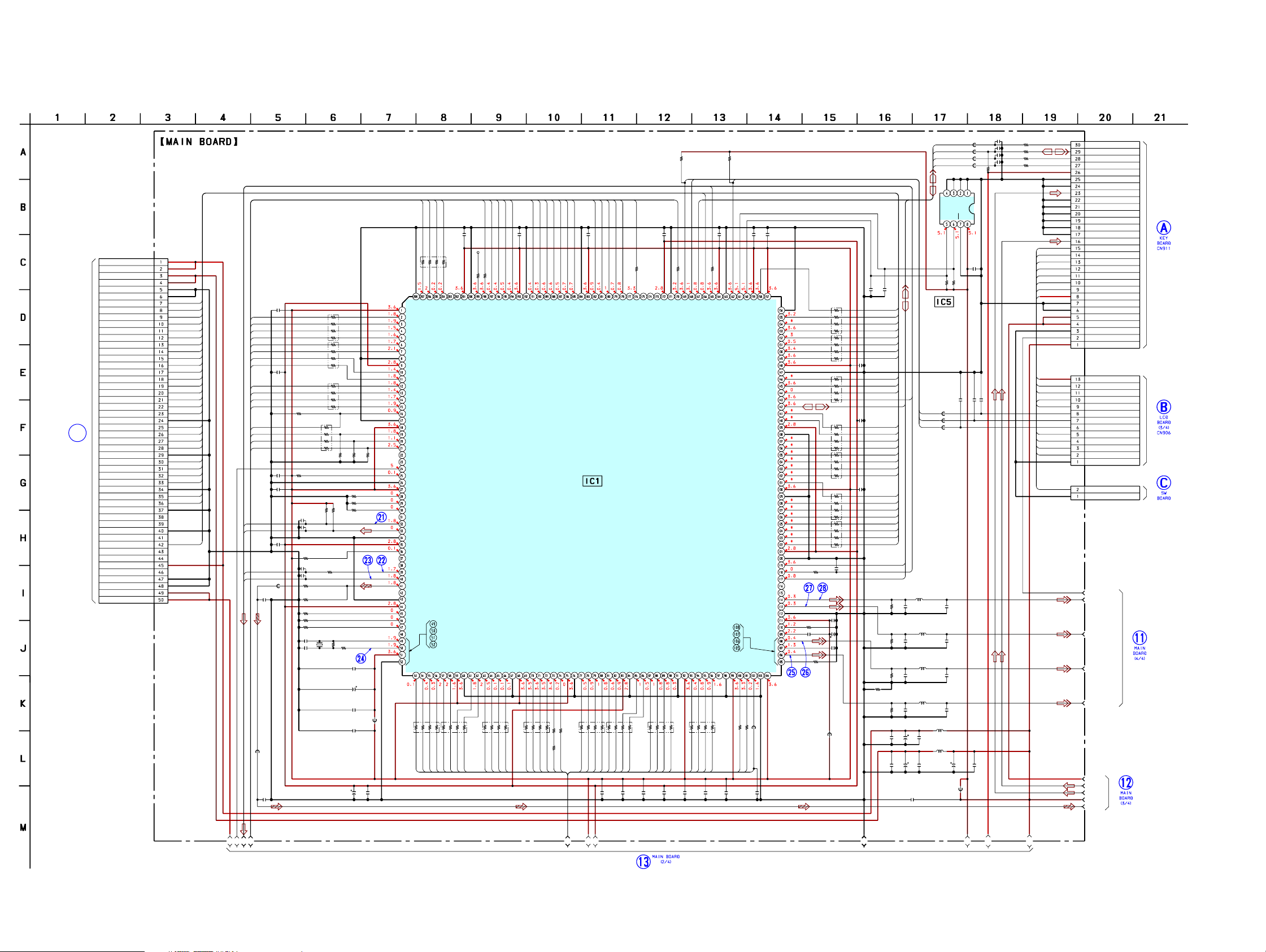
6-7. SCHEMATIC DIAGRAM – MAIN Board (1/4) –
(1/4)
CN101
50P
HIDCS16#
HIORDY
HRST
HD0
HD1
HD2
HD3
HD4
HD5
HD6
HD7
HD8
HD9
HD10
HD11
HD12
HD13
HD14
HD15
HIRQ
HA1
HA0
HA2
HWR#
HRD#
HCS1#
HCS3#
AUX4
C1
0.1
LA4
LA5
LA6
LA7
LA8
LA9
LA10
LA11
C2
0.1
LA12
LA13
LA14
LA15
LA16
LA17
LA18
LA19
C3
0.1
C4
0.1
TWS
TSDO
C7
0.1
MCLK
TBCK
C10
L52
330p
L40
C134 C179
33p 100p
P
SERVO
BOARD
(2/3)
CN1
(Supplement-1
page 13)
+5V
+5V
+5V
+5V
GND
GND
RST
HD0
HD1
HD2
DH3
HD4
HD5
HD6
HD7
HD8
HD9
HD10
HD11
HD12
HD13
HD14
HD15
GND
HINTJ
HA1
HA0
HA2
GND
IORDY
IOWJ
IORJ
HCS1J
GND
HCS16J
HCS3J
GND
LOAD+
LOAD-
GND
SPD_DET
ENDSW
SLOT_OUT_DET
SLOT_IN_DET
PA5V
SPD_STP
GND
GND
SM8V
SM8V
• See page 39 for Waveforms. • See page 47 for IC Pin Function Description.
L
3
5
4
2
L
1
1
1
1
R
D
D
D
D
L
L
L
L
W
C78
0.1
33
33
10
4
3
4
4
R
R
L
L
0
1
EE
IN
IN
V
M
M
A
A
C
C
5
A
S
E
M
E
S
V
D
V
7
6
A
A
H
H
3
5
4
S
H
S
R
V
W
L
X
7
6
A
A
M
M
D
D
0
0
1
1
3
B2
B
R
R
2
L
1
1
1
1
R
D
D
D
D
L
L
L
L
W
L
X
0
1
1
1
8
9
A
A
A
A
S
M
M
M
M
S
D
D
D
D
V
0
1
8
9
1
1
A
A
A
A
H
H
H
H
8
6
9
7
0
1
D
D
D
D
1
1
D
L
S
EE
S
V
V
S
A
C
E
D
E
X
V
3
3
4
B
R
#
S
E
A
K
C
C
L
L
L
L
D
L
8
9
0
7
1
1
1
D
D
D
L
L
L
D
D
L
L
N
0
1
E
S
K
K
_
E
A
N
K
N
R
A
W
C
A
B
S
B
D
D
X
X
D
D
D
3
3
3
3
4
5
2
2
R
R
0
7
2
R
#
0
1
O
K
K
#
S
N
N
E
A
A
A
W
R
B
B
3
5
D
L
5
6
S
D
D
S
L
L
V
MPEG DECODER
ES6008FF
0
S
E
B
E
S
V
D
V
0
1
5
B
R
0
1
B
B
D
D
0
1
2
4
D
D
L
L
4
EE
D
L
V
IC1
1
2
B
B
D
D
3
2
B
B
D
D
#
D
D
D
3
L
L
L
S
C
L
33
42
R
3
0
1
2
D
LD
L
3
4
B
B
D
D
4
B
D
C24 C25 C26 C27 C28 C29 C30 C72
0.1 0.1 0.1 0.1 0.1 0.1 0.1 15p
2
3
S
S
S
D
S
L
LD
V
C
C
L
L
X
X
5
6
7
C
S
B
B
B
C
S
D
V
V
D
D
0
0
1
1
7
6
B
B
R
R
5
6
7
B
B
B
D
D
D
4.7k
R1
R5
RB17
RB18
4.7k
C5
C6
R12
C8
C9
R17
R16
R19
R20
R21
C14 R22X1
11p 100k27MHz
C15
11p
10
10
RB19
10
RB20
10
R2 R3 R4
4.7k 4.7k 4.7k
R10 R11
4.7k 4.7k
100p
100p
4.7k
100p
100p
33
4.7k
100k
100k
100k
1
2
3
0
A
A
A
A
L
L
L
L
RB21
VSS
1
2
3
0
A
A
A
A
L
L
L
L
VEE
LA4
LA5
LA6
LA7
LA8
LA9
VSS
VCC
LA10
LA11
LA12
LA13
LA14
LA15
LA16
VSS
VEE
LA17
LA18
LA19
LA20
LA21
XRESET
TDMDX
VSS
100k
R7
100k
R8
100k
R9
33
R14
R23
1.5k
C18
0.1
C17
10
16V
C19
0.1
L48
C21
0.1
C22
C23
10
100p
16V
VEE
TDMDR
TDMCLK
TDMFS
TDMTSC#
DAC LRCK
DAC DATA
VSS
VCC
SEL_PLL1
NC
NC
DAC MCLK
DAC BCK
SPDIF
NC
VSS
VCC
RSD
RWS
XIN
RBCK
XOUT
NC
AVEE
AVSS
1
4
2
3
0
A
A
A
A
A
M
M
M
M
M
D
D
D
D
D
RB1
10
1
2
4
3
0
A
H
5
A
A
A
A
A
H
H
H
H
H
R68 R66
10k 4.7k
7
#
X
E
U
O
A
L
33
40
R
E
C
1
0
S
O
C
S
S
S
L
V
V
C
C
L
L
X
X
X
0
1
8
9
1
1
S
B
B
B
B
S
D
D
D
V
D
0
1
8
9
1
1
B
B
B
B
D
D
D
D
CN102
BS AUX5
SDIO
INS
SCLK
1
0
D
2
FT
S
S
S
N
3
6
4
5
X
X
U
U
A
A
S
B
E
E
-B
-B
S
C
CK
2
1
E
B
E
V
D
3
2
1
1
B
B
D
D
2
X
X
X
U
U
U
A
A
A
C69C71C74C75
0.10.10.10.1
3
3
9
3
R
W
L
S
E
S
E
S
E
S
B
-B
M
D
V
V
S
A
C
N
A
D
E
M
D
B-Y
VREF C
R-Y
DCLK
#
3
5
1
1
1
14
S
S
E
B
B
B
C
E
S
D
D
V
V
D
D
10
29
R
RB8
10
#
5
4
1
1
B
D
O
B
S
C
D
C66C68
0.10.1
C89
C87
100p
A
2
L
VEE
E
A
D
C
E
S
S
H
V
VSS
HA1
HA0
HCS3FX
XHCS1FX
XHIOCS16
XHRD
XHWR
VEE
VSS
HIORDY
XHRST
HIRQ
MC
MS SDIO
HD15
HD14
VCC
VSS
HD13
HD12
HD11
HD10
HD9
HD8
HD7
VEE
VSS
HD6
HD5
HD4
HD3
HD2
HD1
HD0
VCC
VSS
MS INS
MD
MS SCLK
PCLK2XSCN
YUV7
VBS
Y
ADVSS
ADVEE
RSET
COMP
0
K
S
M
C
C
S
E
Q
S
D
E
S
V
D
D
X
V
10
0
6
3
5
R
L
X
M
K
Q
L
C
D
33
RB16
33
RB15
33
RB14
RB13
RB12
RB11
33
RB10
33
R34
33p
C35
270
R32
0.1
C32
R31
0
L51
100p
HA2
HA1
HA0
HCS3#
HCS1#
HIDCS16#
HRD#
HWR#
C58
0.1
HIORDY
HRST
HIRQ
AUX4 O
SDIO
C52
33
0.1
HD7
HD6
HD5
HD4
HD3
HD2
HD1
33
33
C34
0.1
C33
10
16V
C31
0.1
HD0
C44
0.1
HD15
HD14
HD13
HD12
HD11
HD10
HD9
HD8
INS
EAUX31
SCLK
R72 C99
75 470p
R69
C157
75
470p
R70
C96
75
470p
R33
0
R71
C97
75
470p
C367
C368
10
0.1
35V
C372
C373
10
0.1
35V
A
G
02
5
S
IC
A
C
L
4
C
-2
S
SD
S
R61 R62
1k 1k
EEPROM
p
33
105
C
AUX2
L12
AUX7
L55
AUX6
L11
C100
L3
2.2µH
470p
L50
2.2µH
C79
470p
L1
2.2µH
C95
470p
L2
2.2µH
C98
470p
L308
22µH
C366
1
L309
22µH
C371 C369
C370
100
1 0.1
16V
FB3
C
C
C
V
W
C104
33p
L10
L9
L8
L7
R77
4.7k
C86
0.1
p
33
33p
1
6
0
15
1
C
C
R76
C103
33p
R75
C102
33p
R74
C101
33p
R73
30P
33
33
33
33
IN
RST
EJ
A/D
CONT
TEMP
REM
VCC
VCC
REM
TEMP
SW
CONT
A/D
EJ
RST
IN
SW
MS BS
MS SDIO
MS INS
MS SCLK
MS VEE
MS GND
MS GND
IR RCH
IR GND
IR GND
IR GND
IR GND
IR GND
IR GND
IR LCH
LED DISC IN
RESET
KEY PW/EJ
KEY A/D
IR CONT
TEMP DET
REM
REM VCC
LIGHT GND
LIGHT GND
SW12V
SW12V
KEY GND
LIGHT PW/EJ
LIGHT KEY/GATE
CN103
13P
REMVCC
REM
TEMP-DET
MONITOR SW
IR CONT
DA-BE
CK-BE
CS-BE
KEY A/D
KEY PW/EJ
RESET
LED DISC IN
KEY GND
CN104
2P
MONITOR SW
SW GND
(Page 38)
(Page 34)
(Page 38)
LIGHT-PWEJ
CVBS
Y
B-Y
R-Y
SW12V
IR-L
IR-R
+5V
SPDIF
(Page 29)
(Page 28)
MV-900SDS
4
2
1
3
A
A
A
A
7
5
6
A
A
A
8
A
0
9
1
A
A
11
A
(Page 27)
2626
Page 27
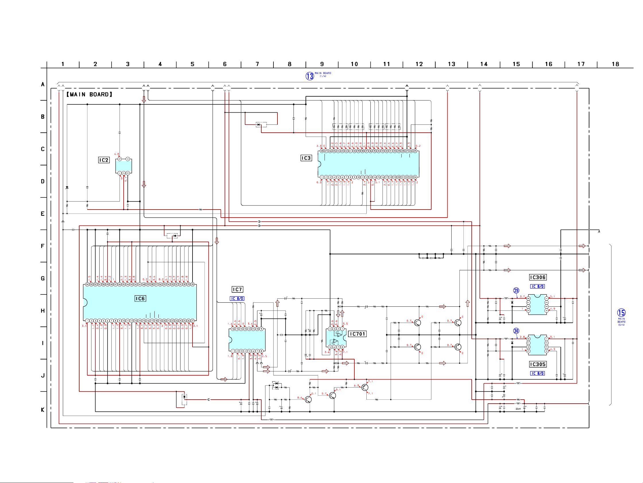
MV-900SDS
6-8. SCHEMATIC DIAGRAM – MAIN Board (2/4) –
A3
A1
A2
(2/4)
C83
0.022
CD NC
GND
VDD
IC2
OUT
MA8068-L-TX
R47
0
RESET SIGNAL
GENERATOR
PST3645NR
C82
C81
1000p
R48 C80 R46
10k 0.1 0
A4
• See page 39 for Waveforms. • See page 41 for IC Block Diagrams.
(Page 26)
A5
A6
A7
LA0
LD7
LD6
LD14
R52
0
10
DQ7
DQ6
GND
DQ15
DQ14
A9
A10
A12
A11
A13
LA10
LA11
LA12
LA13
LA14
D14
RB491D-T146
C84 R54
0.1 0
FLASH ROM
IC3
MBM29LV800TA
-70PFTN
LA17
RB25
A16
BYTE
A14
A15
LA16
LA15
A8
LD1
LD2
LD8
LD4
LD5
LD12
LD13
10
RB24
VCC
DQ5
DQ4
DQ13
DQ12
A8
WE
RST
R49
0
LA9
WRLL
LD9
LD3
LD11
LD10
10
10
RB23
RB22
DQ8
DQ1
DQ9
DQ3
DQ2
DQ11
DQ10
A6
A4
A17
A18
BY#
VPP
WP#
LA8
LA7
LA18
LA19
LA1
LD0
LOE#
OE
CE
GND
DQ0
A2
A4
A3
A5
LA3
LA4
LA5
LA6
LCS3#
A0
A1
LA2
A9
R57
0
R90
4.7k
A10
A11
MD
DGND
FB1
FB2
(CHASSIS)
R1734
0
C177 C178
100p 100p
C794 C795
R727
4700p 4700p
C701
1
R703
50V
22k
C703
R78
33k
C147
10
16V
C793
100p
AGND
VCOM
ZEROR
ZEROL
VDD
VOUTL
VCC
L706
C146
0.1
47
16V
C145
VOUTR
C792
100p
L707
D13
DAN202K
R87
47
R85
R88
220k
220k
C150
C149
10
100p
35V
L54
100µH
1000p
C148
0.1
C702
1
50V
16V
10
47k
47k
C705
R705
R706
16V
220
0.1
C706
C707
C704
1000p
R704
22k
R83R84
33k33k
2SC2412K
R86
120k
DELAY
R709
R711
3.3k
R707
3.3k
R708
3.3k
Q3
22k
C709
150p
GND
C708
150p
R710
3.3k
2SC2412K
VCC
R712
22k
R81 R82
3.3k 100k
Q2
MUTING SWITCH
R713
R715
R719
C711
000
1k
10
16V
C713
100p
R721
4.7k
C715
0.1
LOW-PASS
FILTER
IC701
RC45580R
C710
10
R714
R716
16V
1k
Q1
2SA1037AK
Q1,2
R80
10k
C714
0.1
R722
4.7k
C712
100p
R720
0
Q701
2SC2412K
Q702
2SC2412K
Q701-704
MUTING
0
R723
470
Q703
R725
4.7k
2SC2412K
C717
0.1
C716
0.1
R726
4.7k
Q704
2SC2412K
R724
470
R1710
C790
100p
47k
R1709
C791
100p
47k
R1733
0
SWITCHING REGULATOR
IC306
L312
100µH
R377
150
XC63778103SR
LX
EXT1
EXT2
GND
PBST
VOUT
LX
EXT1
EXT2
GND
PBST
VOUT
IC305
XC63778103SR
SWITCHING REGULATOR
C378
220
16V
VIN
CE
VIN
CE
L314
22µH
R370
56k
R372
1.2k
R371
22k
R368
18k
R369
10k
D321
C396
470p
RB161L-
10TE25
C395
470
16V
L313
22µH
D320
RB161L-
10TE25
C391
2200p
C390
470
16V
C385
0.1
C383
1000p
C381
100
16V
C394
0.1
C389
0.1
C384
100
16V
C382
100
16V
C379 L311 C376C377
0.1
C797
1000p
C796
4700p
C400
0.1
C392
C393
4700p
C388
4700p
0.10.1
10
16V
C387
0.1
C386
10
16V
L-CH_AUDIO
AUDIO_GND
R-CH_AUDIO
(Page 28)
+8V
L41
C135
33p
C94
DB15
DB14
VSS
DQ14
VSSQ
DQ15
DQ1
VCCQ
DQ0
VCC
DB0
DB1
C90 C91
0.1 0.1
0.1
DB9
DB8
DB10
DB11
DB13
DB12
DQ9
DQ8
VCCQ
DQ10
VSSQ
DQ11
DQ12
DQ13
VCCQ
SD-RAM
IC6
HY57V641620HGTP
-HI
DQ7
VSSQ
DQ6
DQ5
VCCQ
DQ4
DQ3
DQ2
VSSQ
DB4
DB2
DB6
DB3
DB7
DB5
D1
RB491D-T146
HA4
HA5
HA6
HA7
HA8
HA9
CLK
CKE
HA11
DQMX
A4
A5
A6
A7
NC
A9
NC
CLK
VSS
DQMH
DQML
VCC
WE
CAS
CAS#
RASO#
WE#
C92
1
A8
CKE
A11
BA1
A10
BA0
RAS0
CS
BANK1
BANK0
HA10
CSO#
HA0
VSS
VCC
A3
A2
A1
A0
HA3
HA2
HA1
D12
RB491D-T146
L53
D/A CONVERTER
IC7
PCM1751DBQR
AUX3
MCLK
AUX4 O
EAUX31
ML
MC
SCK
DATA
LRCK
BCK
TWS
TSDO
TBCK
C144
C143
47
0.1
16V
MV-900SDS
2727
Page 28
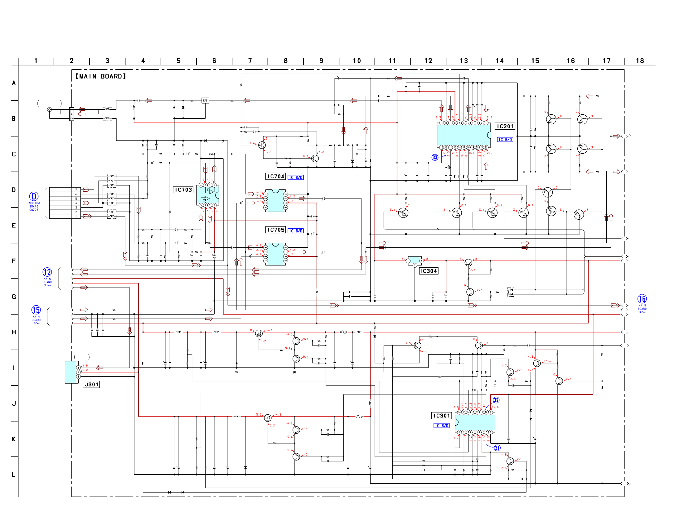
MV-900SDS
6-9. SCHEMATIC DIAGRAM – MAIN Board (3/4) –
(3/4)
(Page 38)
(Page 26)
(Page 27)
FM MODULATOR
ANTENNA
L-CH_AUDIO
R-CH_AUDIO
R+
R-
L-
L+
AUDIOGND
VGND
VIN
AUDIO_GND
SW12V
CN201
3P
CN701
7P
IR-L
IR-R
+5V
SPDIF
+8V
C255
4700p
J301
OPTICAL
OUTPUT
SPDIF
5V
GND
TRANSCEIVER
OPTICAL
C254
4700p
L203
C253
4700p
L202
2.2µH
D204
1SS356
R740
2.2k
C724
4.7
L701
L702
L703
R730
0
R731
0
25V
R736
10k
R734
47k
R737
10k
R735
R745
100k
47k
R739
10k
R741
2.2k
C723
C721
100p
100p
R308
10k
• See page 38 for Waveforms. • See page 41 for IC Block Diagrams.
R212
10k
VCC
C734
22µH
RB050L-40TE25
R220
6.8k
0.047
C221
R213 C220
220 33
10V
Q208
2SK209GR
C718
10
35V
C731
1
100
16V
D302
C320
2200
25V
C719
10
35V
Q301
TPC6102
SWITCHING
REGULATOR
R334 D305
1k 1SS355
L306
22µH
Q304
TPC6102
SWITCHING
REGULATOR
D314
RB050-40TE25
Q208,209
LOW-PASS
S
S
Q302,303
REGULATOR
CONTROL
FILTER
R215
4.7k
AUDIO INPUT SELECT
IC704
NJM2233
GNDVIN1
SWI
VOUT
VIN2
V+
NC
NC
AUDIO INPUT SELECT
IC705
NJM2233
GNDVIN1
SWI
VOUT
VIN2
V+
NC
NC
R304 C306
47 100p
Q303
2SA1576A
S
R311
47
Q306
2SA1576A
R214
R231
2.2k
10
R216C219
Q209
1.5k1
2SC4081
C736
35V
C737
0.1
C738
100
16V
C735
35V
L350
100µH
R302 R301
220 2.2k
Q302
2SC4081
R303
220
Q305
2SC4081
Q305,306
REGULATOR
CONTROL
1500.1
D203 D202
1SS356 1SS356
C720
R742
C722R744
100p100k
R738
10k
R746
12k
2200
25V
1000p 20k 0.01
C726
100p
100k
4.7
25V
DIFFERENTIAL
AMP
IC703
RC45801PWR
R750
22k
C725
4.7
R747
25V
12k
C727
4.7
R749
25V
12k
R743
R754
100k
1k
L304 L303
22µH
R306
82k
R305
C313
15k
0.01
R313
68k
C324
C325 R312 C321
R314
10
22k
35V
D315D316
1SS3551SS355
FL201R221C225
D304 D303
UDZS5.6B UDZS5.6B
R748 C730
R752
22k
12k 1
GND
R751
22k
R753
R755
22k
1k
C732
C733
47
0.01
16V
C309C314
C310
470
0.01
25V
C212
1
C217
10
35V
C218
330p
R211
10k
C224R218R217
R219
82p3.3k3.3k
10k
C223
C222
2200p
KV1471ETR
10
10
2A 72V
C307
C305
100p
0.01
R307
2.2k
R309
220
C317
100p
R310
220
C318
100p
10p
D201
F301
L201
100nH
C251
4700p
C252
4700p
L302
22µH
C304
470
25V
L305
22µH
F302
1A
72V
C315
C316
470
0.01
25V
R209
18k
C214 R232
33p 33
C216
0.01
R210
2.2k
Q210 Q211 Q212 Q213
DTC144EUA DTC144EUA DTC144EUA DTC144EUA
FM-CE
C346 C345
0.1 0.1
R333
1k
D306
1SS355
R332 R331
1k 47k
C213
C215
0.01
1000p
VTIN
RFGND
RFOUT
XIN
XOUT
VCC
X201
C227 C228
0.01 0.1
+5V REGULATOR
R330
220
R317
R319
C327
7.6MHz
-CLK
FM
C344
22
16V
R326
39k
POWER CONTROL
IC301
BA9743AFV
39k
18k
0.47
22p
C229
C230
C348 R324
0.01 10k
C226
100
16V
R227 R228 R229 R230
4.7k 4.7k 4.7k 4.7k
Q210-213
LEVEL SHIFT
IC304
XC6202P502PR
OGI
Q313
2SA1576A
LATCH
22p
100
R223
2SA1797
VCC
CE
100
R224
Q324
Q323
2SC4081
PD
CLK
100
R225
R365
10k
2SC4081
SWITCHING
VREF
CT
35V
10
C211
GND
MPX ADJ
ATT
DATA
100
R226
C231 C232
150p 2200p
FM-DATA
Q312
39k
R325
SCP
NON2
NON1
CR
150p
C210
VC
SEP
Q323,324
B+ SWITCH
470p
C350
C330
470p
INV2
INV1
2200p
C209
RLPF
LLPF
39k
R321
FB2
FB1
C347
470p
C351R315R316C326
470p39k22k220p
REMP
LEMP
R367
47k
DT2
DT1
RIN
LIN
470k
R322
R323 C331
OUT2
OUT1
R366
22k
R364
10k
2SA1576A
18k 0.47
VCC
GND
R318
27k
FM STEREO
MODULATOR
Q314
DEAD
TIME
IC201
BH1415F
D317
DAN202K
R327
47k
R329
22k
C332
2.2
C329
0.15
Q310
2SA1576A
R320 C349
47k 2.2
1SS355
1SS355
C201
C203
4700p
4700p
C202
2SA1797
D307
D308
Q201-204
RF LEVEL
1
C204
1
C333
1
Q309
R328
47k
SWITCHING
R203
2.2k
Q201
DTC144EUA
R201
2.7k
R202
2.7k
C328
10
35V
Q202
DTC144EUA
R204
2.2k
Q205
DTA144EUA
BUFFER
Q207
DTC144EUA
INVERTER BUFFER
R378 R380
R379
4.7k
47k 4.7k
Q309,311
B+ SWITCH
Q311
2SC4081
R207
10k
R205
3.3k
Q203
DTC144EUA
B1
Q204
DTC144EUA
R206
R208
3.3k
10k
Q206
DTA144EUA
FM2
FM1
R381
22k
B2
B3
B4
B5
B6
B7
B8
B9
B10
B11
(Page 29)
MV-900SDS
2828
Page 29
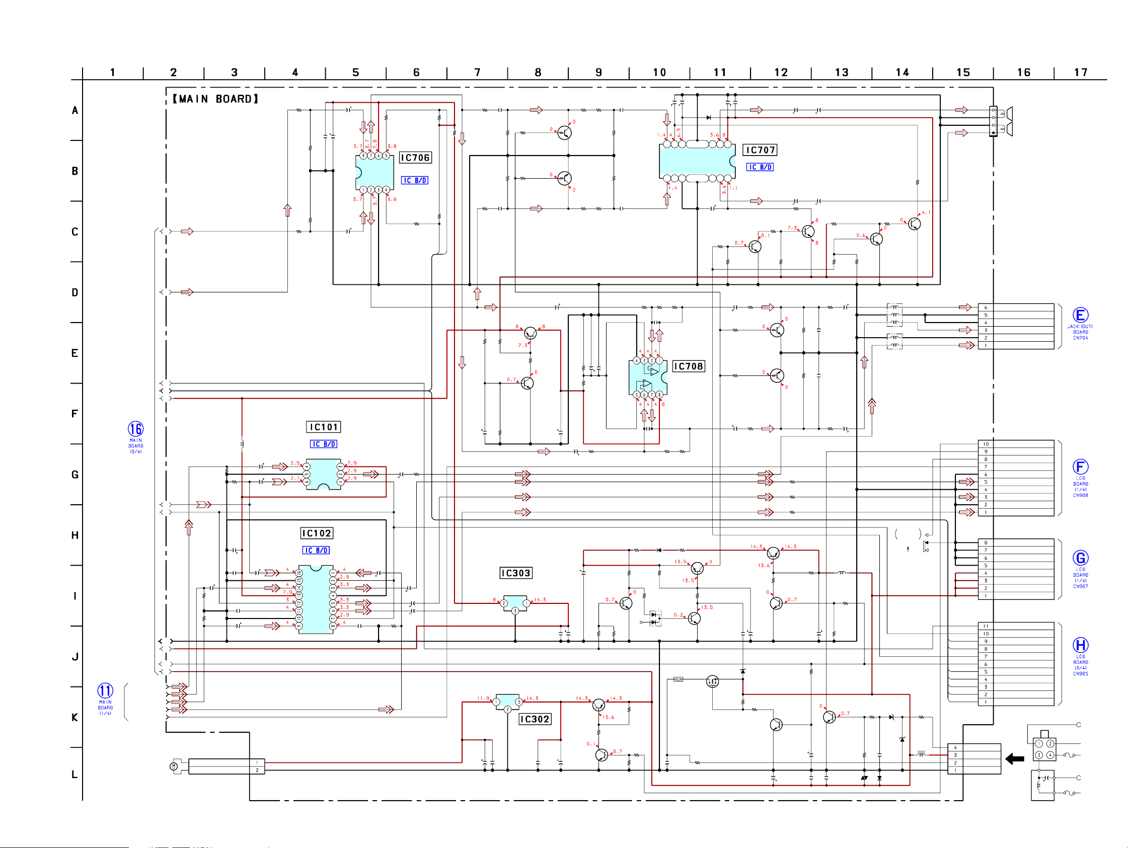
MV-900SDS
6-10. SCHEMATIC DIAGRAM – MAIN Board (4/4) –
MV-900SDS
(Page 26)
(Page 28)
LIGHT-PWEJ
• See page 41 for IC Block Diagrams.
4.7
25V
GND
GND
POWER
GND
POWER
Q325
TPC6102
R383
D701
1SS133
MUTING SWITCH
R356
15k
0
C759
16V
C757
NC
NC
22
R782
R783
4.7k
Q318
2SA1576A
Q325,326
B+ SWITCH
10
35V
VCC
LOUT
ROUT
STBY
STANDBY SWITCH
10k
S
Q710,711
C771
4.7
25V
R797
2.2k
R796
2.2k
C772
4.7
25V
C363
2.2
R384
150k
Q710
2SC4081
C758
0.1
POWER AMP
R795
100
R792
100
UDZS5.6B
R385
150k
IC707
LA4627
Q713
DTC314TU
MUTING
Q712
DTC314TU
MUTING
C364
1
50V
D313
CN705C762 C764
4P1000 10V 1000 10V
R1769
D310
MA8068-L
L704
L705
Q715
2SC4081
D309
UDZS-308
POWER
SELECT
680
CN702
6P
CN108
10P
S301
B
A
R339
4.7k
L301
CN301
FM1
FM2
FM-CLK
FM-DATA
FM-CE
S-SCK
S-SDA
4P
ACC
BATT
AMP REN
BATT GND
CN107
CN105
8P
11P
C761 C763
1000
1000
10V
10V
R781
10k
R784
1k
Q711
2SA1576A
R785
10k
R798
22k
R799
22k
R109
0
R110
0
R111
0
Q319
2SB1694
Q320
2SC4081
Q319,320
POWER ON
MUTING
Q326
2SC4081
C397
C301
2200
25V
R1767 R1768
10k 4.7k
R1701
100
C773
100p
C774
100p
R1702
100
R360R359
100k10k
C365
47
25V
R386
22k
ACCESSORY
47
16V
C302 C303 D301
0.01 100 1N5404TU
DISCHARGE SWITCH
2SC4081
R1765 R1766
10k 10k
C775
10
35V
C776
10
35V
L307
47µH
R362
10k
R361
100k
Q315
2SC2412K
DETECT
R341 C339
4.7k 0.1
VDR301
Q714,715
Q714
R340
10k
RCH
AUDIOGND
AUDIOGND
LCH
VGND
VOUT
A MUTE
SW1
FM1
FM2
AMP ON
POWER ON
FM-CLK
FM-DATA
FM-CE
S-SCK
S-SDA
SP1
(L-CH)
SP2
(R-CH)
FAN CONT
ACC IN
ACC SW
LIGHT PW/EJ
V GND
Y/CVBS
V GND
R-Y
V GND
B-Y
GND
GND
GND
GND
BATT
BATT
BATT
BATT
(Page 38)
(Page 32)
(Page 32)
(Page 34)
GND
AMP REM
ACC
F304
1A
GND
BATT
F303
5A
R789 R791 R793
10k 6.8k 12k
GND
C768
100p
R357
0
1SS356 0
R355
15k
R354
10k
D318
DAN202K
R338
22k
R335
10k
C755 C756
100
16V
9
10 11 14 15 16
DC
P.P
LIN
RINNCPRE
876 321
C767
100p
LINE AMP
IC708
NJM4558V
VCC
R790 R794
6.8k 12k
D312 R358
Q316,317
MUTING
CONTROL
Q317
2SC4081
TH301
C398
0.15
(4/4)
C748
R762 C744
4.7k 10
C746
0.01
R764
6.8k
R765
B1
B2
B3
B4
B5
L101
22µH
R105
75
C166
100
16V
C167
0.01
10 35V
C161
10 35V
C162
10 35V
C176
10
35V
C174
0.1
C173
CN302
2P
R104
75
B6
B7
C175
10
35V
R107
75
R108
75
B11
B8
B10
B9
CVBS
R-Y
B-Y
Y
M301
(FAN)
FAN+
FAN-
R763
4.7k
VIDEO INPUT SELECT
VIDEO INPUT SELECT
NJM2283V
IN1A
GNDI
IN2B
V+
SW2
IN2A
GND3
IN3B
6.8k
GND
VIN1
IC102
IC101
MM1508
IN1B
SW1
OUT1
GND2
OUT2
OUT3
SW3
IN3A
35V
C745
220
16V
C743
10
35V
V+VIN2
VOUT
SW
R766
100
1
C
T1
LK
C
U
C
V
LIN
LO
T1
A
1
D
U
N
O
IN
AT
D
R
R
G
C168
10
35V
R106C172
750.1
ELECTRICAL
C165
470
16V 75
C169
VOLUME
PT2257
10
35V
C170
10 35V
C171
10 35V
R768
4.7k
IC706
R769
4.7k
R767
100
A
K
D
D
-S
-S
S
S
R103
10
R761
R770
R771
R345 R343
10k 10k
C338
47
25V
R772
100k
R773
100k
C747
1k
Q321,322
POWER ON
C343
47
25V
NJM78L12UA-TEJ
C337 C336
0.1 0.1
111k
MUTING
R344
47k
+8V REGULATOR
IC303
TA78DL08AF
OGI
IC302
OGI
R774
10k
R775
10k
+12V REGULATOR
R342
2SB1694
1k
2SC4081
C765
4.7
25V
Q321
Q322
C342
10
35V
C341
0.1
C335
22
16V
R787
4.7k
R786
4.7k
C766
4.7
25V
C340
47
25V
C750
0
Q708
DTC314TU
MUTING
Q709
DTC314TU
MUTING
C749
0
Q308
2SA1797
Q307
2SC4081
R776
10k
C752
1
R778
2.2k
R779
2.2k
C751
R777
1
10k
25V
47
0.1
C770
C769
R788
10k
C362
R353
220
22k
25V
Q316
2SC4081
R352R351
22k3.3k
Q307,308
R337
10k
B+ SWITCH
R336
47k
2929
Page 30
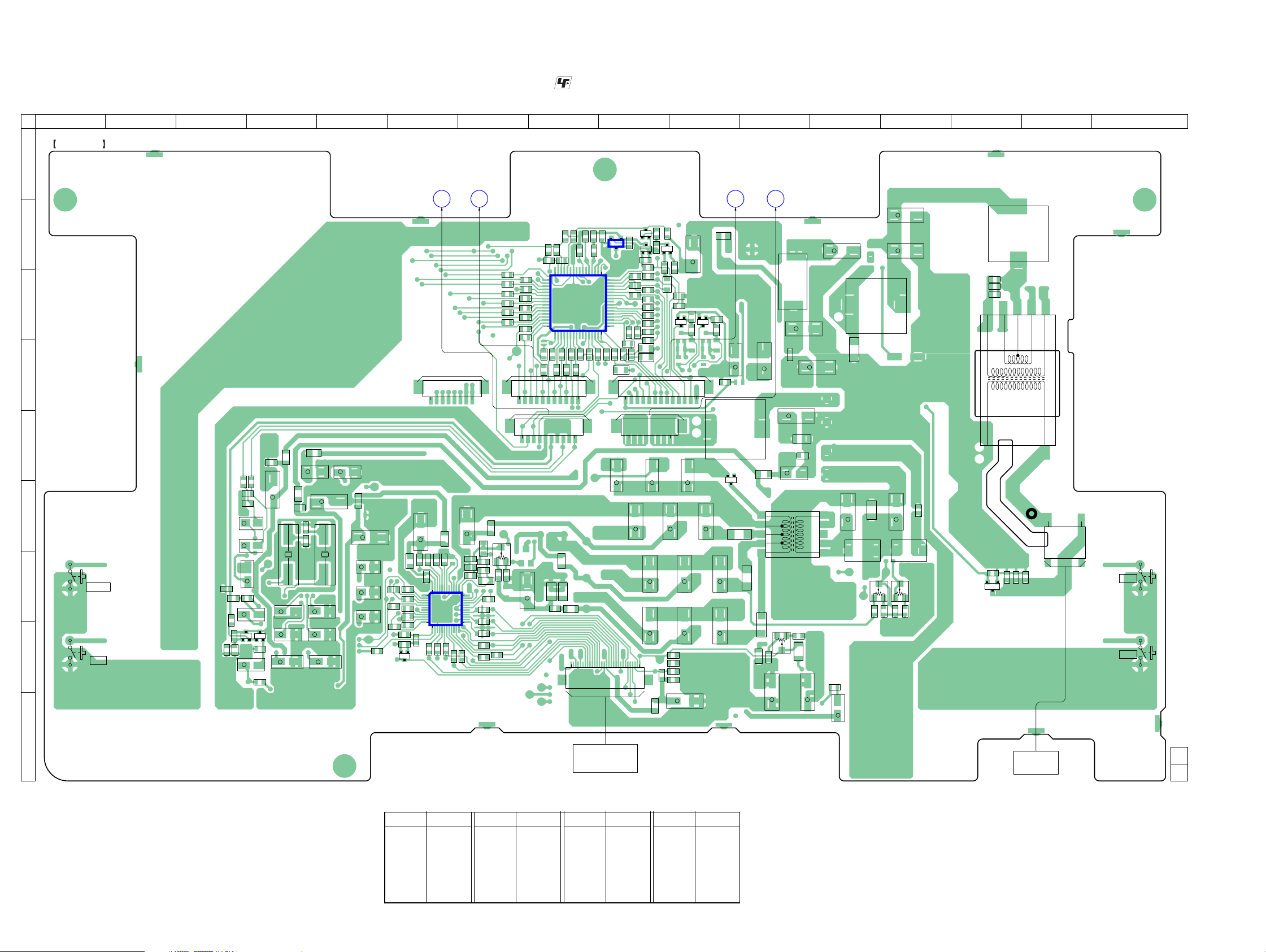
MV-900SDS
6-11. PRINTED WIRING BOARD – LCD Board (Side A) –
1 2 3 4 5 6 7 8 9 10 11 12 13 14 15 16
LCD BOARD
(SIDE A)
A
B
C
D
E
C502
R539
R537
C501
R540
+
R538
F
S402
G
H
REVERSE
S403
MENU
R518
R525
R517
C532
R516
C533
C541
Q502
+
C504
+
C505
C544
+
+
C536
Q503
ECB
ECB
R515
+
C531
R514
L402
L501
+
L502
C514
C546C547
X502 X501
+
C511
+
C507
+
C529
C483
+
+
• See page 23 for Circuit Boards Location.
(Page 24) (Page 24)
MAIN
BOARD
CN108
F
8
+
C481
+
C515
L503
R609
R610
R612
Q603
R601
R603
R606
R607
R608
C608
+
R642
R639
R638
L606
C609
1
IC601
12
R611
R614
R615
BCE
+
C522
+
C516
R602
+
C517
C513
C512
+
C525
R604
+
C520
R507
CN909
L601
R637
R616
MAIN
BOARD
CN105
H
NC
1
C604
+
KA
D602
C658
C657
C606
R633
R643
L604
3748
36
R630
FL603
FL602
25
2413
FL601
R621
R620
R619
R617
R618
R432
R438
R439
R440
R442
R443
R444
R445
R446
R447
R448
R472
R449
11 1
10
L602
RV601
R661
R660
C660
+
R460 R434
49
54
R450 R494
CN905
CN908
: Uses unleaded solder.
R433
R498
R430
R497
C407
2
IC403
32
R429
Q402
R477 R427
R426
R424
C551
R435
R471
48 33
13
C409
IC401
17
R495
16
R479
R411
R412
R413
R416
R417
AK
D954
13 1
81
C829
+
CN801
R662
1
R402
C610
R403
R404
L603
C659
L605
R405
R406
1
R407
R473
R408
C827
+
Q403
R462
R496
130
R461
R425
R423
R422
R421
R420
R419
R418
CN907
(Page 24) (Page 24)
MAIN
BOARD
CN103
B
ECB
R493
ECB
ECB
R492 R470
Q401
R456
R455
AK
D402
C412
C963
BCE
Q953
AK
D955
AK
D956
CN906
C817
+
C826
+
C831
+
C833
+
C845
C837
R830
R829
C836
+
C835
L812
C823
+
C820
+
R499
C405
+
Q955
R959
R955
BCE
R956
R960
R964
L950
C816
D801
+
C825
+
C822
+
C819
+
K
D804
C959
+
D803
AK
AK
D950
D802
L803
AK
BOARD
CN107
C957
+
AAAK
MAIN
G
L850
+
F850
+
C955
C954
+
C962
T801
DC/DC CONVERTER
RV802
R842
R841
C841
+
C956
C851
C844
+
+
C839
C850
R849
+
C852
C838
+
L851
KA
D851
C806
C805
+
L801 L802
RV803 RV801
R832
R833
+
+
C809
+
C813
C860
C859
R801
F801
D852
R866
R865
R864
C864
K
A/K
L852
T850
INVERTER
TRANSFORMER
A
R870
R869
TP853
R868
CN850
12
S404
VOL +
S401
VOL –
I
MV-900SDS
• Semiconductor Location
Ref. No. LocationRef. No. Location
D402 C-10
D602 F-7
D801 E-10
D802 G-11
D803 G-11
D804 F-11
D851 D-12
D852 G-14
D950 E-11
D954 D-9
D955 D-9
D956 D-9
IC401 C-8
LCD1
LIQUID CRYSTAL
DISPLAY MODULE
Ref. No. Location Ref. No. Location
IC403 B-9
IC601 G-6
Q503 H-4
Q603 H-6
Q953 C-10
Q401 B-9
Q955 C-10
Q402 B-9
Q403 B-9
Q502 H-3
3030
BACK LIGHT
UNIT
1-863-447-
11
(11)
Page 31

MV-900SDS
6-12. PRINTED WIRING BOARD – LCD Board (Side B) –
1 2 3 4 5 6 7 8 9 10 11 12 13 14 15 16
LCD BOARD
(SIDE B)
A
B
C865
C
Q857
BE
C
EB
Q858
C
C863
D
E
TP854
D853
Q861
Q860
R877
R876
BCE
R871
R875 R855
R874
R878R872
BCE
R873
C883R889
R886
C880
KA
R884
R882
R883
R856
Q853
R885
F
R815R814
16 9
IC801
G
R469
C801
R803 C802 R805
C803
R802
H
D461
AK
R466
C463
I
• See page 23 for Circuit Boards Location.
C404
+
R454
R451 R452
R453
F950
DDS
DDG
Q951
IC950
R840
C842
4
1
R847
Q807
Q804
R838R836
C450
IC951
1
C958
C950
R951
R952
Q952
C951
3
TP804
C818 C821
BCE BCE
R839R837
S
D
D
D
R858
D
G
Q856
BCE
BCE
R857
Q854
C886
16 9
IC850
18
C884
C885
R893
R892
R890
R891
+
C952
+
C953
R813
R816
R817
C810
C812
C811 R812
C807
R811
C808
BE
R804
TP802
R810
R809
R806
R807
C804
Q801
2E
2B
1C
R808
Q806
L813
R844
1 8
2C
1B
1E
R859
R846
Q802
ECB
ECB
R863
R860
C857
R861
C858
C
Q803
R845R848
Q855
BCE BCE
Q859
F951
1
2
Q805
2C
2E
1B
2B
R843
1E
1C
TP828
C840
C843
5
8
IC802
: Uses unleaded solder.
C408
R428
TP805
IC402
TP951 (–)
L809
TP819
TP810
R475
R474
C403
C402
8 5
1 4
D805
R831
X401
TP812
TP811
KA
R415
C832
R431
C401
R414
D952
TP832
D806
KA
C830
R436
R530
R437
R401
KA
D951
TP987
TP983
IC405
C650
+
C654
IC602
1
8
4
5
TP602
R651
R652
R653
R655
KA
C828
C834
C651
R658
R657
R654
C653
C652
R631
TP601
R659
R632
C605
R635
R634
C607
D601
L607
R624
R625 R627
R641
R640
BCE
AK
Q601
R605
R613
R490
R491
11
20
TP506
R489
R663
R501
R502
C518
C519
R503
C521
C484
TP403
L403
R488
C523
Q501
Q506
R506
R487
R504
R505
TP405
C486
C485
10
R485
C482
R483
1
C480
R481
R486
17
32
BCE
R508
D501
C534 R523
R522
BCE
R524
R482
R480
C510
C509
IC501
C524
AK
R521
Q505
R484
C527
C508
BCE
R510
C506
116
4833
C528
C526
R513R509
C503
Q504
C530
TP513
TP510
R529
C545
C543
64
C542
C540
C539
R526
49
C535
L504
C537C538
ECB
R528
R527
R512
R511
R519
R520
R467
R468
11
1-863-447-
(11)
R478
R458
C406
L401
R476
KA
D401
3
2
ECB
R953
R954
C824
L806
L805
3
C815
C960
C961
2
1
L807
TP807
R457
IC952
TP952 (+)
L804
L808
TP808
L810
TP806
L811
MV-900SDS
• Semiconductor Location
Ref. No. LocationRef. No. Location
D401 C-7
D461 I-4
D501 H-13
D601 G-11
D805 G-9
D806 G-9
D853 D-4
D951 E-9
D952 E-9
IC402 D-8
IC405 F-12
IC501 G-13
IC602 F-10
Ref. No. Location Ref. No. Location Ref. No. Location
IC801 G-4
IC802 I-6
IC850 D-5
IC950 E-6
IC951 D-7
IC952 D-7
Q501 H-12
Q504 H-13
Q505 I-13
Q506 I-13
Q601 G-11
Q801 G-5
Q802 G-6
Q803 H-5
Q804 H-5
Q805 H-5
Q806 H-5
Q807 H-5
Q853 C-5
Q854 C-5
3131
Ref. No. Location Ref. No. Location
Q855 C-6
Q856 C-5
Q951 D-6
Q952 E-7
Q857 C-3
Q858 C-2
Q859 C-6
Q860 C-4
Q861 B-4
Page 32

MV-900SDS
6-13. SCHEMATIC DIAGRAM – LCD Board (1/4) –
(1/4)
TP983
TP987
CN908
CN907
10P
TP951
(-)
8P
TP952
(+)
B1
B2
B3
B4
B5
(Page 29)
(Page 29)
FAN CONT
ACC IN
ACC SW
LIGHT PW-EJ
V GND
Y/CVBS
V GND
R-Y
V GND
B-Y
GND
GND
GND
GND
BATT
BATT
BATT
BATT
• See page 39 for Waveforms. • See page 41 for IC Block Diagrams. • See page 47 for IC Pin Function Description.
R519 R520
4.7k 4.7k
D501
1SS356
16V
V-SCK
V-SDA
22
R516
15k
V-SDA
PONRST
COMDC
SECAM BLACK ADJ
YIN
CTRAPOUT
CTRAPIN
YDET
ACCDET
CIN
VCC1
GND3
KILLDET
APCDET
SCOUT
VXO-NTSC
VXO-PAL
+5V REGULATOR
IC951
TA78DL05AF
G
100
R512
I
Q502
2SC4081
C532
0.22
Q502,503
SYNC
SEPARATOR
R517C533R518
33k14.7k
R525
0
C537
27p
L504
C538
12p
Q504
2SC4081
PAL/NTSC
SWITCH
R537
3.9k
R539
2.2k
F950L950
Q951,952
B+ SWITCH
2A
C952
1000p
25V
R951
150k
R952 C951
150k 0.15
Q952
2SC4081
S
Q951
TPC6102
C950
1
B6
10µH
R953
10k
R954
100k
F951
47µH
R527 R528
47k 4.7k
0
B7
Q503
2SC4081
C531
4.7
25V
R515
1k
C535
2.2
C536
4.7
25V
C539
C540
C541
C542
C545
0.022
C954
1000
0.15
25V
C960 C961
1 0.1
B8
R526
0.1
0.1
0.1
0.1
C543
TP513
C955
47
25V
+3.3V REGULATOR
XC6206P332MR
2.2k
0.1
R529C544
5.1k1 50V
X501C546
3.58MHz9p
X502C547
4.43MHz10p
R538
3.3k
R540
3.3k
IC952
OGIO
TP510
C501
C502 C503
47
0.1 0.1
16V
+8V REGULATOR
IC950
TA78DL08AF
OI
G
R513R514
220k330
L501
47µH
10
35V
1
1500p
C528
C529
C530
100
511
R
K
IN
IN
C
C
C
N
N
V-S
Y
ISY
CS
AV
N
T
T
U
U
O
IN
O
LN
-Y
-Y
-Y
A
P
B
R
R
35V
35V
2.2
2.2
C504
C505
C956
1
C958
0.15
16V
1M
0.47
22
0.022
8
R50
C526
C525
C524
0.022
5.6k
10k
27
C5
R509
R510
1
2
J
C
D
C
A
V
O
C
V
1
IN
-Y
CC
B
V
0.1
C506
C962C953
10
35V
B9
ET
D
FC
A
RGB DECODER
AN2546FH-AV
F
E
VR
V
35
2.2
C507
C957C959
47
25V
K
D
C
FLT
N
O
L
G
LK
C
N
BC
+
SY
H
IC501
1
1
-IN
-IN
-IN1
R
G
B
50V
1
0.1
0.1
0.1
C511
C508
C509
C510
B10
Q501
2SC4081
BUFFER
L
T
S
IN
GB
O
U
VS
P
R
VD
50V
1
512
C
D950
1SS356
CO
N
Y
S
C
T
2
2
E
ET
-IN
-IN
-D
-D
G
G
R
B
50V
1
513
C
100
R480
SCLK
N
T
E
-D
R
R521 R524
10k 10k
Q505
2SC4081
C523
1800p
R523
22k
33k
R505
100
R507
R504
82k
100
486
R
1
2
R
2
LK
C
V
K
VC
V
BL
V B
T
U
T
C
O
D
D
M
D
V
C
10k
485
R
16V
10
TP403
C483
D
C IN
N
SC
S
EST
G
T
O
O
C486
5p
C485
33p
L403
22µH
C484
33p
11
B
P
C
S
HDOUT
VDOUT
RWMOUT
VCOMOUT
R-OUTDET
VREFDRIV
G-OUTDET
B-OUTDET
2
-IN
B
R-OUT
G-OUT
B-OUT
100
R481
CSN
R506
100k
VCC3
VCC2
GND1
BLAK
YS
100
100
100
100
100
489
R491
R490
R
R488
R487
N
VG
VB
CN
C
N
YN
SY
V
HS
A
T
LK
L
N
A
C
C
S
S
C
D
P
10k
100
482
R
DATA
R483
16V
10
100k
100p
0.1
C481
R484
C480
C482
A1
Q505,506
SYNC DET
R503
R502
R501
C534
1
TP506
0.1
0.01
OSD DRIVER
IC405
µPD6467
TP405
2.2 35V
47
2.2 35V
47
2.2 35V
47
C515
47
16V
C514
0.1
Q506
2SC4081
L402
22µH
GREEN
C522
47
16V
POL
HD
VD
C521
1
RED
BLUE
HD
VD
R522
10k
C520
C519
C518
C517
C516
L502
K1
L
B
L503
47µH
A2
A3
A4
(Page 33)
A5
A6
A7
C1
C2
C3
C4
C5
(Page 35)
C6
2
B1
B13
B14
MV-900SDS
(Page 34)
3232
Page 33

6-14. SCHEMATIC DIAGRAM – LCD Board (2/4) –
(2/4)
A1
A2
A3
A4
F850
1A
32V
C850 C851 C852
100
25V
TFT-ON
DIMMER
L850
100µH
47
25V
10µH
100
25V
R662L605
0
R855
22k
C660
22
35V
• See page 39 for Waveforms. • See page 41 for IC Block Diagram. • See page 47 for IC Pin Function Description.
PHASE
IC602
Q855
2SC4081
Q859
2SA1576A
Q855,856,859
SWITCHING
REGULATOR
S
L851
10µH
Q856
CPH6316
R863
220
D851 R876R877
RLS245 22k10k
C653
560p
R653
47k
R654
4.7k
R871
1.5k
R874
22k
Q860,861
DIMMER
C884
POWER CONTROL
2SA1576A
C880
0.1
Q860
0.1
1IN+
1IN-
FEDBCK
OUT-
DTC
CTRL
CT
RT
GND
C1
IC850
TL594
R875
10k
C859
100
25V
C860
100
25V
R882
4.7k
C652
0.1
R883
R657
R658
68k
1M
R655
22k
10k
C883
R891
12k
R892
10k
C885
R893
Q861
2SC4081
R884 R885 R886 D853
7.5k 22k 22k RLS4148
R889
0.1
33k
R890
12k
1000p
10k
R858
47k
Q854
Q853,854
B+ SWITCH
2SA1576A
R659
10k
D602
1SV231
C657
C658
1000p
0.1
L603
10µH
C654
R857
47k
Q853
2SC4081
R856
100k
R660
2.2k
RV601
47k
R661
C659C610
2.2k
0.150.15
R859
2.2k
R860
220
C857
100p
R861
220
C858
100p
TP601
2
C
D
D
N
IN
V
1
IN
R651
68k
R652 C651
TP602
0.1
2.2k 0.1
CONPARATOR
S
S
V
NJU7071V
C650
1000
10V
L852
100µH
R864 R865 R866
3k 3k 3k
R878
1k
R872
18k
R873
22k
2IN+
2IN-
REF
VCC
C2
E2
E1
C863
0.1 100V
C865
8200p
100V
Q857 Q858
2SC4672 2SC4672
Q857,858
OSC
C886
0.1
T850
INVERTER
TRANSFORMER
TP854
MV-900SDS
TP853
CN850
2P
3k
3k
3k
R868
R869
R870
D852
DAN217
C864
1
BACK LIGHT
UNIT
(Page 32)
R625
47k
L
2
R
TV
S
100
100
100
R632
R631
R630
L602
A5
A6
A7
10µH
R633
L604
1.8µH
470k
L
1
D
E
O
VCO0
VSS
RST
HDOT1
WH(UONS)
HPOS4
HPOS3
HPOS2
HPOS1
NP1
VDD
VSS
D
S
C
V
M
V
Z
D
V
Q
)
2
E
ID
(S
IN
L
C
IN
E
N
C
S
Y
N
H
S
Y
P
S
H
C
100
100
R601
R602
2
E
D
O
D
H
M
C604
47
16V
L601
10µH
R641
22k
T
S
JU
C607
4.7
D601
RB501V-40TE
C608
47
16V
R640
22k
C605 C606
0.1 56 p
L607
0
R634
27k
L606
0
C609
Q601
2SC4081
INVERTER
R643
220
100
R635
100
R637
100
R638
100
R639
0.1
R642
2.2k
D
P
LCD CONTROLLER
)
1
E
ID
(S
L
E
S
H
Q
100
100
R603
R604
E1
D
O
D
M
V
T
E
S
S
O
P
IN
B
D
V
IC601
MN5814
2
T
T
S
O
U
J
D
H
T
T
U
U
O
O
H
V
R624
100
1
2
L
2
V
H
H
R
T
P
P
S
C
C
QH(ZOOMC)
1
K
2
3
S
S
C
S
O
A
O
O
L
P
P
P
B
V
V
V
100
R605
100
100
100
100
R609
R606
R607
R608
ZOOM
1
H
P
C
FL603 FL602 FL601
3
H
P
C
STH2
STH1
OEH
STV1
OEV1
OEV2
OEV3
CPV
INTEXT
POL
)
UD
X
M
O
O
B
O
T
(Z
L
R610
100
D
U
3
2
H
PH
C
CP
R627
100
R621
100
R620
100
R619
100
R618
100
R617
100
R616
100
R615
100
R614
100
R611
22k
R612
22k
L
O
P
Q603
2SC4081
INVERTER
STH2
STH1
OEH
STV1
OEV1
OEV2
OEV3
CPV
R613
4.7k
UD2
LR
R663
0
MV-900SDS
D1
D2
E1
E2
(Page 34) (Page 35)
E3
E4
3333
Page 34

MV-900SDS
6-15. SCHEMATIC DIAGRAM – LCD Board (3/4) –
(3/4)
CN905
CN906
11P
FM-DATA
UDZS5.6B
D951
UDZS5.6B
D952
13P
R964
0
D954
UDZS5.6B
D955
UDZS5.6B
D956
UDZS5.6B
DA-BE
CK-BE
CS-BE
(Page 29)
(Page 26)
AMUTE
SW1
FM1
FM2
AMP ON
POWER ON
FM-CLK
FM-DATA
FM-CE
S-SCK
S-SDA
REMVCC
REM
TEMP DET
MONITOR SW
IR CONT
DA-BE
CK-BE
CS-BE
KEY A/D
KEY PW/EJ
RESET
LED DISC IN
KEY GND
• See page 39 for Waveform. • See page 47 for IC Pin Function Description.
SWITCH
Q403
2SC4081
Q402
R492
100k
Q401
2SA1576A
R455
R457
R458
D402
1SS356
B8
L401D401
RB501V-40
R456
10k
22k
1k
22k
R493R470
47k10k
R471
68k
10µH
C407
1000p
R466
1000p
AMP ON
PW-ON
FM-CLK
FM-CE
S-SCK
S-SDA
B5
B4
B2
AMUTE
SW1
FM1
FM2
Q953
2SA1576A
LED DRIVE
R956
10k
Q955
2SA1576A
LED DRIVE
R960
10k
B6
R955
22k
RESET
Q401,403
WAKE UP
R959
22k
C963
0.1
2SC4081
R461
22k
INVERTER
R462
22k
VPP
(Page 32)
10
B
CSN
0
0
00
1
1
422
421
R
20k
2
475
R
0
0
1
R474
R
D2
N/P
XIR
AVSS
VD
IC401
N
M
O
R
SIDE2
L
ZO
TFT O
CS-BE
CK-BE
DATA
SCLK
0
0
0
00
00
10
10
10
1
1
420
417
419
R
T
YNC-DE
S
ER
M
IM
D
R416
R
R418
0
0
0
479
496
R
R
R495
LK
ATA
C
D
D
SD
O
OS
NC
JUST
-BE
K-BE
C
CS
DA(OUT)-BE
DA(IN)-BE
DISC_LED
LIGHT PW/EJ
FAN CONT
FM-DATA
N
1
P O
M
W
A
S
S-SDA
S-SCL
FM-CE
FM-SCK
PW-ON
SCK
SO
SI
R408
100
SCL
SDA
VDD1
VSS
TEST
R
CS
D
OS
IDE1
S
DA-BE
0
00
10
1
100
2
3
1
41
411
R
R
R4
C401
1
R473
100
R407
100
R406
100
R405
100
R404
100
R403
100
R402
100
R401
47k
R494
BP6
C412
1000p
00
1
100
425
426
R
R
SW
R
ITO
N
O
M
V-SCK
B9
00
00
1
1
424
423
R
R
/EJ
VD
-D
KEY IN
KEY
EY PW
K
SYSTEM CONTROLLER
µPD780023AGK-C36-9ET-A
E
UT
M
U/D
A
V-SDA
R478
220k
R476
220k
TEMP
AVREF
AVDD
RESET
XT2
XT1
IC
X2
X1
VSS1
VD
KEY HALT
REM HALT
ACC IN
REM IN
IR CONT
B1
00
100
1
7
42
477
R
R
ET
Y/N
D
CC
PW
A
1
2
FM
FM
B7
R452
R451
15k
68k
C450
0.1
R454
R453
22k
18k
C406
1
C405
47
16V
C408
0.1
C409
0.1
R429
10k
R430
100
1k
R460
22k
X401
4.19MHz
C551
R428
100
R432
R433
R434
R435
R497
R498
RESET SIGNAL
GENERATOR
IC403
XC61CN2702MR
OI
G
0
0
0
R431
100
100
100
100
R436
100 1k
B3
B11
C404
0.1F
3.5V
R499
0
R415
C403
0.1
4.7k
R414
4.7k
IC402
S-24C02BFJ
C402
0.1
S-SDA
S-SCK
FM-CE
FM-DATA
FM-CLK
PW-ON
VCC
E0
EEPROM
B12
VD
L
A
CN
SC
SD
W
VSS
E2
E1
(Page 33)
2
1
D
B13
D
B14
(NC)
MV-900SDS
VPP
RESET
SCK
SO
SI
VDD
GND
CN909
R467 R468 R469
470 820 2.2k
C463
8P
VPP
RESET
SCK
SO
SI
0.1
UDZS5.6B
D461
S401
-
S403S402
MENUREVERSEVOL
00
00
00
00
00
00
00
1
100
1
100
1
438
R
V-SCK
R439
V-SDA
440
R
AMUTE
1
442
R
UD
7
43
530
R
R
S404
VOL
+
FM2
FM1
00
1
1
1
1
3
444
44
445
446
R
R
R
R
TFT-ON
MODE2
LR
ZOOM
00
1
447
R
MODE1
00
1
448
R
DIMMER
00
00
1
1
100
449
450
R472
R
R
988
AMP ON
SW1
TP
JUST
3434
Page 35

MV-900SDS
6-16. SCHEMATIC DIAGRAM – LCD Board (4/4) –
(4/4)
C3
C2
C838
10
R849
(Page 32)
C1
C5
C4
16V
L813
10µH
F801
1A
32V
R813
18k
C810
0.47
TP828
L802
150µH
39k
C839
C840 R848
47
0.1 39k
16V
V+
R836
12k
R837
39k
C841
47
16V
R814R815 R817C812
220k1k 39k0.47
C811
470p
R816
39k
• See page 39 for Waveforms. • See page 41 for IC Block Diagram. • See page 47 for IC Pin Function Description.
E1
E2
R842R843R844R845
12k22k4733k
Q803-807
V COM BIAS
Q803
V COM AMP
IC802
NJM4558M-TE2
V-
C843
0.1
C842 R838 R839
0.1 56k 47
R812
33k
C809
47
25V
C808
0.15
2SC4081
Q804
2SA1576A
Q806
2SC4081
-1 -2
Q805
R840
22k
SB007W03Q-TL
IMZ1A
RV802
47k
R841
C845
47k
0.033
L803
10µH
D801
L804
47µH
TP805
C844
R846
4.7
4.7k
R847
4.7k
Q807
2SA1576A
(Page 33)
E3
C835
C836 C837 R830
47
0.1 0.1 4.7k
16V
RED
GREEN
BLUE
C828
C830
0.1
C827
25V
L808 L809 L810 L811
10µH10µH10µH10µH
0.1
C829
47
47
25V
R831
L812
10µH
D805
1SS356
C832
C831
R829
4.7k
0
D806
1SS356
C834
0.1
0.15
C833
47
25V
47
25V
E4
CN801
30P
STH1
TP810
TP811
TP812
OEH
CPH1
CPH2
CPH3
RL
STH2
TP819
STV2
OEV3
OEV2
OEV1
CPV
UD2
STV1
TP832
VCOM
SHT1
VB
RED
GREEN
BLUE
OEH
VDD1
MODE
CPH1
CPH2
CPH3
RL
STH2
VCC
VSS
VCOM
STV2
OEV3
OEV2
OEV1
CPV
U/D
STV1
NC
VEE
VSS
VDD1
NC
VHG
LCD1
LIQUID
CRYSTAL
DISPLAY
MODULE
MV-900SDS
C816
C815
0.15
T
-
+
EF
CP
S
R
+
T
1IN
R
RV801
CT
10k
R801
3.3k
IC801
BA9743AFV
R802
39k
R804
18k
C803
C6
0.47
U
TC
CC
K
V
BCK
2IN
2IN
C
2O
2D
B
T
D
-
1IN
D
U
TC
2FED
N
R806
1O
1D
G
1FE
C802
470p
R803 R805C801
39k 33k470p
TP802
2.2k
R807
33k
C804
470p
R808
33k
R809 R810 C805
1.2k 1.2k 0.15
-1 -2
Q801
IMZ1A
2SD1760Q
Q801,802
DC/DC
CONVERTER
Q802
L801
150µH
C806
47
25V
C807
470
100V
R811
0
T801
DC/DC CONVERTER
C813
220p
D802
RLS245
D803
RB160L
D804
RB160L
C818
0.15
R832
47k
RV803
10k
R833
12k
C821
0.15
C824
0.15
C817
47
47
25V
25V
L805
47µH
C819
C820
47
47
25V
25V
L806
47µH
C823
C822
100
47
25V
25V
L807
47µH
C825
C826
47
47
25V
25V
TP804
TP806
TP807
TP808
3535
Page 36

MV-900SDS
6-17. PRINTED WIRING BOARD – PANEL Section (1/2) –
1 2 3 4 5 6 7 8 9 10 11 12 13 14 15
A
B
KEY BOARD
(COMPONENT SIDE)
16
CN912
D908
J
C
D
FRONT BOARD
CN910
(Page 37)
S904 – 907
1
3
64
• See page 23 for Circuit Boards Location.
R910
13
46
S905
R907
13
46
S904
R906
KA
C913
: Uses unleaded solder.
R912
13
46
S907
u
110
11
(11)
MS FLEXIBLE
BOARD
CN913
MEMORY STICK
CONNECTOR
MEMORY
STICK
1-863-446-
13
R908
S906
46
+
C918
+
C928
C932
+
C934
+
+
C930
+
C924
+
C925
C922
+
C926
+
C920
+
MAIN BOARD
CN102
(Page 24)
IC901
1-863-446-
D909
KA
R913
34
21
11
(11)
E
KEY BOARD
F
G
(CONDUCTOR SIDE)
D915
R921
C941
R920
D916
R932
R933C942
3
IC903
2
C923
1
C921
D914
CN911
D912
D911
R925
R926
E
B
RV900
E
RV901
B
IC902
(IR TRANSMITTER)
3
1
D910
D911 – 916
R919
C917
AK
C929
IC904
C931
R922
R918
R923
C927
18
169
C933
Q901
BCE
R917
Q903
C
Q904
E
C
R934
BCE
R928
R927
D913
Q902
C
R931
R930
B
Q905
A
H
• Semiconductor Location
Ref. No. LocationRef. No. Location
D908 B-4
D909 G-15
D915 F-5
D916 G-9
D910 G-8
D911 G-7
D912 F-11
D913 F-6
D914 F-10
IC901 G-15
IC902 G-8
IC903 F-10
IC904 F-8
MV-900SDS
Ref. No. Location
Q901 G-8
Q902 F-7
Q903 E-7
Q904 F-6
Q905 F-6
3636
Page 37

MV-900SDS
6-18. PRINTED WIRING BOARDS – PANEL Section (2/2) –
1 2 3 4 5 6 7 8 9 10 11 12 13 14 15
FRONT BOARD
(COMPONENT SIDE)
A
KA
D900
POWER
B
KA
C
D
D902
DISC IN
FRONT BOARD
1
CN910
R903
(CONDUCTOR SIDE)
7
S901
RESET
R905
• See page 23 for Circuit Boards Location.
D900 – 903
AK
: Uses unleaded solder.
D903
KA
DISC SLOT
ILLUMINATION
D901
EJECT
KA
1-863-448-
11
(11)
R904
R901
R902
E
C
WHT
S903
EJECT
MAIN BOARD
CN104
(Page 24)
SW BOARD
(SIDE B)
11
1-863-449-
(11)
• Semiconductor
Location
Ref. No. Location
D900 B-2
D901 B-14
D902 C-1
D903 B-8
D917 H-2
D918 H-3
D919 H-4
D920 H-10
D921 H-9
D922 H-9
1-863-448-
11
(11)
S902
POWER
F
G
H
I
J
(Page 36)
KEY BOARD
CN912
JACK (IN) BOARD
MAIN BOARD
CN701
D
(Page 24) (Page 24)
C947
D918
L703
C948
7
L706
L705
L704
KA
J701
INPUT
C946
1
CN703
L702
L701
R937
KA
D917
VIDEO AUDIOL R
D919
MAIN BOARD
CN702
E
C954
C953
C952
L709
L710
L711
6
CN704
L712
R939
AK
D921
AUDIOL R
KA
D920
1-863-444-
11
(11)
SW BOARD
(SIDE A)
S908
PANEL CLOSE
DETECT
(ON: CLOSE)
1-863-449-
BLK
11
(11)
D922
1
AK
L707
J702
OUTPUT
L708
JACK (OUT) BOARD
KA
1-863-443-
11
(11)
VIDEO
MV-900SDS
3737
Page 38

MV-900SDS
6-19. SCHEMATIC DIAGRAM – PANEL Section –
MEMORY
STICK
MEMORY
STICK
CONNECTOR
MS FLEXIBLE BOARD
R908
2.2k
R907
820
R906
470
GND
VEE
SCLK
-
INS
-
SDIO
VEE
BS
GND
S907
S906
S905
S904
CN913
10P
R912
68
C913
0.1
D908
R910
68
UDZS5.6B
R919
47
• See page 41 for IC Block Diagram.
TEMPERATURE
SENSOR
IC901
REMOTE CONTROL
RECEIVER
IC902
RPM714C-V4
D
T
C
N
U
C
O
G
V
C918
C917
47
0.01
16V
S-8120CNB
R913
47
R918
4.7k
R917D910
22kMA8068-L
R933
R932
2SC4081
1k
1k
Q901
SIRCS
BUFFER
CN911
30P
MS BS
MS SDIO
MS INS
MS SCLK
MS VEE
MS GND
MS GND
IR RCH
IR GND
IR GND
IR GND
IR GND
IR GND
IR GND
IR LCH
LED DISC IN
RESET
KEY PW/EJ
KEY A/D
IR CONT
TEMP DET
REM
REM VCC
LIGHT GND
LIGHT GND
SW12V
SW12V
KEY GND
P
C
N
TEM
D
C
N
VC
G
D909
UDZS5.6B
CN912
LIGHT PW/EJ
LIGHT KEY/GATE
7P
LIGHT GATE
LED DISC IN
LIGHT PW/EJ
LIGHT GND
KEY PW/EJ
RESET
KEY GND
(Page 26)
(Page 29)
AUDIO
INPUT
VIDEO
R
L
(CHASSIS)
R+
R-
L-
L+
VGND
VOUT
J701
A8068-L
A8068-L
M
M
917
D918
D
CN704
6P
A8068-L
M
D919
0.1
C954
L706
0
0
L705
0
L704
0
L703
0
L702
0
L701
0.1
0.1
0.1
48
C9
C947
C946
R937
0
0
L712
0
L711
0
L710
0
L709
0
L708
0
L707
0.1
0.1
952
953
C
C
R939
0
CN703
A8068-L
M
D920
7P
A8068-L
M
D921
A8068-L
M
D922
R+
R-
L-
L+
AUDIOGND
VGND
VIN
J702
(CHASSIS)
R
L
VIDEO
(Page 28)
AUDIO
OUTPUT
MV-900SDS
47k
1000p
R920
C941
IR TRANSMITTER
MODULATOR
TA2061AF
R921C942
47k1000p
IC904
+8V REGULATOR
IC903
TA780L08AF
16V
16V
47
47
1M
10k
0.1
0.1
923
C932
C934
R
R922
C931
C933
C924
1
50V
C
C
G
LIN
EFC
A
C-T/C
VR
F
AG
-
TO
IX-N
IN
FF
AU
M
R
O
C925
1
50V
16V
50V
22
0.1
0.1
1
C929
C928
C927
C926
T
W
-R
C
U
V
F0
LO
F0-S
D
T
N
U
D
R
O
N
R
SU
F0-L
G
RV900
100k
(FREQUENCY)
16V
10
C930
C922
C923
100
0.1
16V
RV901
100k
(FREQUENCY)
Q902 Q903
2SD1760Q 2SD1760Q
OGI
C920
C921
47
0.15
25V
R930
47k
Q904 Q905
Q904,905
B+ SWITCH
D911-916
(IR TRANSMITTER)
LED DRIVELED DRIVE
R931
4.7k
D915D916
DAL5821DAL5821
D913
DAL5821
D911
DAL5821
R925R926
2222
2SA1797 2SC4081
D914
DAL5821
D912
DAL5821
R934
0
R928
22k
R927
4.7k
D903
SML-3100TT86
DISC SLOT
ILLUMINATION
SML-3100TT86
SML-3100TT86
D902
DISC IN
D901
EJECT
D900
SML-512M
POWER
R905
2.2k
R904
150
R903
680
R902
150
R901
150
S902S903
POWEREJECT
RESET
S901
CN910
7P
LIGHT GATE
LED DISC IN
LIGHT PW/EJ
LIGHT GND
KEY PW/EJ
RESET
KEY GND
S908
PANEL CLOSE
DETECT
(ON:CLOSE)
(Page 26)
3838
Page 39

• Waveforms
p
p
p
p
p
p
p
132 ns
3.7 Vp-p
– MAIN Board –
MV-900SDS
IC1 es (DAC LRCK)
wa
2 V/DIV, 20 µs/DIV
IC1 el (DAC MCLK)
ws
59.2 ns
2 V/DIV, 20 ns/DIV
IC1 r; (DAC BCK)
wd
22.4 µs
3.7 Vp-
3.7 Vp-
3.7 Vp-
IC1 <zzc (Y)
wj
IC1 <zzv (VBS)
wk
IC306 8 (LX)
wl
1.1 Vp-p
H
500 mV/DIV, 20 µs/DIV
1.2 Vp-p
H
500 mV/DIV, 20 µs/DIV
6.2 Vp-
IC201 qd (XOUT)
ed
2 V/DIV, 2 µs/DIV
IC1 t; (XOUT)
wf
IC1 <z/n (R-Y)
wg
IC1 <z/, (B-Y)
wh
474 ns
2 V/DIV, 200 ns/DIV
4.4 Vp-
37.2 ns
2 V/DIV, 20 ns/DIV
820 mVp-p
H
500 mV/DIV, 20 µs/DIV
IC305 8 (LX)
e;
IC301 7 (OUT1)
ea
IC301 q; (OUT2)
es
3.4 µs
2 V/DIV, 2 µs/DIV
6.2 Vp-p
3.2 µs
2 V/DIV, 2 µs/DIV
14.4 Vp-
4.7 µs
5 V/DIV, 2 µs/DIV
500 mV/DIV, 20 µs/DIV
H
880 mVp-
14 Vp-p
4.7 µs
5 V/DIV, 2 µs/DIV
39
Page 40

MV-900SDS
– LCD Board –
IC501 ts (YIN), tj (CIN)
1
(Color Bars)
H
500 mV/DIV, 20 µs/DIV
IC501 tf (CTRAPIN)
2
(Color Bars)
H
500 mV/DIV, 20 µs/DIV
IC501 yd (VXO-NTSC)
3
282 ns
100 mV/DIV, 100 ns/DIV
1.5 Vp-p
1.2 Vp-p
0.3 Vp-p
Q857, 858 (Collector)
q;
15.2 µs
20 mV/DIV, 10 µs/DIV
IC850 qa (C2)
qa
8.8 µs
5 V/DIV, 5 µs/DIV
IC401 r; (X2)
qs
240 ns
2 V/DIV, 100 ns/DIV
32 Vp-p
12.2 Vp-p
3.4 Vp-p
IC601 qf (POL)
7
IC601 ed (PD)
8
63.6 µs
IC601 eh (VCO1)
9
127 µs
1 V/DIV, 50 µs/DIV
2 V/DIV, 20 µs/DIV
3.8 Vp-p
4.2 Vp-p
3.8 Vp-p
Q801-2 (Base)
qd
Q801-1 (Base)
qf
12.6 Vp-p
4.1 µs
5 V/DIV, 5 µs/DIV
10.2 Vp-p
4.1 µs
5 V/DIV, 5 µs/DIV
40
41 ns
2 V/DIV, 20 ns/DIV
Page 41

• IC Block Diagrams
– MAIN Board –
IC7 PCM1751DBQR
MV-900SDS
SCK
16
SYSTEM
CLOCK
MANAGER
SYSTEM
CLOCK
ML
MC
15
14
13
FUNCTION
CONTROL
INTERFACE
SERIAL
INPUT
INTERFACE
1 2 3
BCK
DATA
MD
LRCK
IC101 MM1508XNRE
1SW
2OUT
6dB
DRIVER
3VCC
ZEROL
SAMPLING
WITH
FUNCTION
ZEROR
11
12
ZERO DETECT
8 TIME OVER
DIGITAL FILTER
CONTROLLER
CLAMP CLAMP
BIAS
ENHANCED
MULTI-LEVEL
DELTA-SIGMA
MODULATOR
IN1
6
GND
5
IN2
4
D/A
CONVERTER
D/A
CONVERTER
POWER SUPPLY
VCOM
AGND
10
9
OUTPUT AMP AND
LOW-PASS FILTER
OUTPUT AMP AND
LOW-PASS FILTER
7 84 5 6
VCC
VDD
DGND
VOUTL
VOUTR
IC201 BH1415F-E2
L-CH INPUT
PRE-EMPHASIS TIME CONSTANT
22 21 20 19 18 17 16 15 14 13 12
LPF TIME CONSTANT
PILOT SIGNAL ADJUST
AUDIO MUTING
DATA
CLOCK
CHIP ENABLE
X'TAL OSCILLATOR
X'TAL OSCILLATOR
PLL VCC
IC102 NJM2283V-TE1
GND
1X
1
A
2
X
3
4
Y
5
Z
6
C
7
OZ
8
0X
16
GND
15
1Y
14
VCC
13
B
12
0Y
11
GND
10
1Z
9
SHIFT REGISTER
–
+
PRE-EMPHASIS
& LIMITER
1 2 3 4 5 6 7 8 9 10 11
R-CH INPUT
L. P. F.
MPX
L. P. F.
+
–
PRE-EMPHASIS TIME CONSTANT
MUTE
VCC
2
FILTER
LPF TIME CONSTANT
0
DETECTOR
+
GND
COMPOSITE SIGNAL OUTPUT
1
50
1
1
19
2
PHASE
VCC
PLL PHASE DETECTOR OUTPUT
1
4
PROGRAM COUNTER
OSC
RF
RF GND
RF OSCILLTOR
RF OUTPUT
41
Page 42

MV-900SDS
1
STBY
2
OUT2
3
NC
4
PRE GND
5NC6
IN2
9
P.P
8
DC
7
IN1
VCC
OUT1
NC
POWER
AMP
RIPPLE
FILTER
+
–
POWER
AMP
REF
AMP
+
–
TSD
PROTECTOR
STANDBY SWITCH
POP SOUND
PROTECTION
BLOCK
12 11 10
IC301 BA9743AFV-E2
CT
1
TRIANGLE
RT
2
OSCILLATOR
ERROR AMP 1
3
NON1
INV1
FB1
DT1
OUT1
GND
4
5
6
7
8
+
–
S.C.P. COMP
+
+
–
PWM COMP1
PWM COMP2
VREF
VREF
–
+
+
–
+
+
R
U.V.L.O.
S R
TIMER LATCH
VREF
ERROR AMP 2
REFERENCE
VOLTAGE
+
–
IC706 PT2257-S
RIN
1
16
VREF
15
SCP
ROUT
2
VSS
3
SDA
4
14
NON2
13
INV2
12
FB2
11
DT2
10
OUT2
9
VCC
+
−
CONTROL UNIT
−
+
−
+
LIN
8
7
LOUT
VDD
6
5
SCL
IC305, 306 XC6377B103SR
VIN
1
BUFFER,
DRIVER
EXT/2
2
P_BST
3
CE
4
IC704, 705 NJM2233BM
BIAS
1VIN 1
2SW 1
3VIN 2
4NC
COMPARATOR
GENERATOR,
BUFFER
COMPENSATION
PWM
RAMP WAVE
OSC
PHASE
8 GND
7V OUT
6V+
5NC
PWM/PFM
CONTROLLER
PROTECTION
ERROR
AMP
REFERENCE
VOLTAGE,
SOFT START
IC707 LA4627-E
LX
8
EXT/1
7
GND
6
FB
5
42
Page 43

– LCD Board –
IC405 µPD6467GR-546-E1
CLK
1
2
CS
3
DATA
4
PCL
5
VDD
CMDCT
6
DATA INPUT
SHIFT
REGISTER
INSTRUCTION
DECODER
CONTROL SIGNAL
DISPLAY CONTROL
DATA REGISTER
BACK GROUND CONTROL
DATA REGISTER
OUTPUT INSTRUCTION
DATA
1bit x 336 word
REVERSE DATA
1bit x 336 word
BLINK DATA
1bit x 336 word
VIDEO RAM
COLOR DATA
3bit x 336word
CHARACTER DATA
9bit x 336 word
CHARACTER GENERATOR ROM
12 x 18bit x 512 word
20
VSYNC
19
HSYNC
18
VB
17
VG
16
VR
15
VBLK
14
VC2
13
OUTPUT CONTROLLER
BLK2
12 VC1
11 BLK1
MV-900SDS
OSCOUT
OSCIN
TEST
GND
DATA
SELECTOR
WRITE
ADDRESS
COUNTER
HORIZONTAL
ADDRESS
REGISTER
CHARACTER
SIZE
REGISTER
7
8
9
10
OSCILLATOR
HORIZONTAL
ADDRESS
COUNTER
HORIZONTAL
POSITION
COUNTER
HORIZONTAL
SIZE
COUNTER
VERTICAL
ADDRESS
REGISTER
VERTICAL
ADDRESS
COUNTER
VERTICAL
POSITION
COUNTER
VERTICAL
SIZE
COUNTER
SYNC
GUARD
43
Page 44

MV-900SDS
IC501 AN2546FH-AV
RST
COM DC
DAC-OUT
Y-IN
TRAP-OUT
Y DET
ACC DET
C-IN
VCC1
GND3
KILL DET
APC DET
SCP-OUT
VXO1
VXO2
LOGIC
F DET
PRGB38VSS
37
INVERT
GAMMA
CONTRAST
BRIGHT
OSD SWITCH
CLAMP
EXT POL
36
LIMIT
VDB IN35HSS
34
–
+
–
+
–
+
33
LOGIC
PWM
VCOM
+
–
+
–
+
–
SCP OUT
32
HD
31
VD
30
PWM
29
VCC3
28
COMMON OUT
27
R-CH AVE DET
26
R-OUT
25
VCC2
24
AVE
23
GND1
22
G-CH AVE DET
21
G-OUT
20
B-CH AVE DET
19
B-OUT
BLAK
18
YS
17
HFO
HSS-IN46NAVI SYNC-IN
SCLK
DAT
47
48
IIC BUS
LOGIC
49
DAC
50
51
DAC
CLAMP
52
53
55
ACC DET
56
57
58
59
60
61
62
63
64
BPF
APC
VXO
SYNC
SEPARATOR
SWITCH
TINT
VXO
GENERATOR
VCC1
43
44
45
VCO L/N
HHKILL
SYNC
CUT
ACC
AMP
R-Y, B-Y DEMODULATOR
KILLER
V SYNC
DROP
VERTICAL
COUNT
DELAY
YUV
SWITCH
42
PHASE
COMP
GCA
AFC DET
41
REGULATOR
GND
VDD
40
REGULATOR
G-Y
GENERATOR
GCASHARPNESS
LDET
39
LOGIC
MATRIX
INTERNAL/
EXTERNAL
SWITCH
1
VXO3
2
R-Y OUT
3
B-Y OUT
4
R-Y IN
5
B-Y IN
6
VCC1
7
VREF
9
10
R-IN 18G-IN 1
B-IN 1
12
13
B-CH DET
R-CH DET11G-CH DET
15
16
R-IN 214G-IN 2
B-IN 2
44
Page 45

IC801 BA9743AFV-E2
MV-900SDS
NON1
INV1
FB1
DT1
OUT1
GND
CT
RT
1
TRIANGLE
2
OSCILLATOR
ERROR AMP 1
3
+
–
4
5
6
7
8
S.C.P. COMP
+
+
–
VREF
VREF
PWM COMP1
–
+
+
PWM COMP2
–
+
+
R
U.V.L.O.
S R
TIMER LATCH
VREF
ERROR AMP 2
REFERENCE
VOLTAGE
+
–
16
VREF
15
SCP
14
NON2
13
INV2
12
FB2
11
DT2
10
OUT2
9
VCC
IC850 TL594INSR
ERROR
1
2
3
4
5
6
7
8
AMPLIFIER 1
+
–
PWM
COMPALATOR
CTC
COMPALATOR
1IN+
1IN–
FEEDBACK
DTC
CT
RT
GND
C1
OSCILLATOR
0.7mA
PULSE-STEERING
FLIP-FLOP
C1 1D
REFERENCE
REGURATOR
UNDER
VOLTAGE
LOCKOUT
CONTROL
ERROR
AMPLIFIER 2
+
–
16
2IN+
2IN–
15
14
REF
OUTPUT CTRL
13
12
VCC
C2
11
E2
10
E1
9
45
Page 46

MV-900SDS
– KEY Board –
IC904 TA2061AF-EL
VREFC
LIN
15
16
14
AGC
AGC-T/C
13
VCC
12
f0-R10f0-SW
11
LOUT
9
1
RIN
REFERENCE
VOLTAGE
+
2
MIX AMP
MIX-NF
AGC
AGC
+
–
LEVEL
DETECT
LEVEL
DETECT
+
+
O. S. M.
PRE-
EMPHASIS
PRE-
EMPHASIS
3
4 5
AUTO-OFF
GND
VCO
VCO
BUFFER
BUFFER
6
f0-L
7
SURND
8
ROUT
46
Page 47

• IC Pin Function Description
MAIN BOARD IC1 ES6008FF (MPEG DECODER)
Pin No. Pin Name I/O Description
1 VEE — Power supply terminal (+3.6V)
2 to 7 LA4 to LA9 O Address signal output to the flash ROM
8 VSS — Ground terminal
9 VCC — Power supply terminal (+2.8V)
10 to 16 LA10 to LA16 O Address signal output to the flash ROM
17 VSS — Ground terminal
18 VEE — Power supply terminal (+3.6V)
19 to 21 LA17 to LA19 O Address signal output to the flash ROM
22, 23 LA20, LA21 O Address signal output terminal Not used
24 XRESET I System reset signal input from the reset signal generator “L”: reset
25 TDMDX O TDM transmit data output terminal Not used
26 VSS — Ground terminal
27 VEE — Power supply terminal (+3.6V)
28 TDMDR I TDM receive data input terminal Not used
29 TDMCLK I TDM clock signal input terminal Not used
30 TDMFS I TDM frame sync signal input terminal Not used
31 XTDMTSC O TDM output enable signal output terminal Not used
32 DAC LRCK O L/R sampling clock signal output to the D/A converter
33 DAC DATA O Serial data output to the D/A converter
34 VSS — Ground terminal
35 VCC — Power supply terminal (+2.8V)
36 SEL_PLL1 I PLL clock frequency setting terminal Not used
37, 38 NC — Not used
39 DAC MCLK O Master clock signal output to the D/A converter
40 DAC BCK O Bit clock signal output to the D/A converter
41 SPDIF O Digital audio signal output terminal
42 NC — Not used
43 VSS — Ground terminal
44 VCC — Power supply terminal (+2.8V)
45 RSD I Audio receive serial data input terminal Not used
46 RWS I Audio receive frame sync input terminal Not used
47 RBCK I Audio receive bit clock signal input terminal Not used
48 NC — Not used
49 XIN I System clock input terminal (27 MHz)
50 XOUT O System clock output terminal (27 MHz)
51 AVEE — Power supply terminal (+3.6V)
52 AVSS — Ground terminal
53 to 58
59 VEE — Power supply terminal (+3.6V)
60 VSS — Ground terminal
61 to 66
67 VSS — Ground terminal
68 VEE — Power supply terminal (+3.6V)
69 XDCAS O Column address strobe signal output to the SD-RAM
70 DSCK_EN O Clock enable signal output to the SD-RAM
71 XDWE O Write enable signal output to the SD-RAM
DMA0 to DMA5
DMA6 to
DMA11
O Address signal output to the SD-RAM
O Address signal output to the SD-RAM
MV-900SDS
47
Page 48

MV-900SDS
Pin No. Pin Name I/O Description
72 XDRAS O Row address strobe signal output to the SD-RAM
73, 74
75 VEE — Power supply terminal (+3.6V)
76 VSS — Ground terminal
77 to 82 DB0 to DB5 I/O Two-way data bus with the SD-RAM
83 VCC S Power supply terminal (+2.8V)
84 VSS — Ground terminal
85 to 90 DB6 to DB11 I/O Two-way data bus with the SD-RAM
91 VSS — Ground terminal
92 VEE — Power supply terminal (+3.6V)
93 to 96 DB12 to DB15 I/O Two-way data bus with the SD-RAM
97 XDCS1 O Chip select signal output terminal
98 VSS — Ground terminal
99 VEE — Power supply terminal (+3.6V)
100 XDCS0 O Chip select signal output to the SD-RAM
101 DQM O Mask signal output terminal for data output to the SD-RAM
102 DSCK O Serial data transfer clock signal output to the SD-RAM
103 VSS — Ground terminal
104 VEE — Power supply terminal (+3.6V)
105 DCLK I Serial data transfer clock signal input terminal Not used
106 R-Y O Video signal (R-Y) output terminal
107 VREF C I Capacitor connection terminal for internal reference voltage
108 B-Y O Video signal (B-Y) output terminal
109 COMP I Compensation input terminal
110 RSET I DAC current adjustment resistor input terminal Not used
111 ADVEE — Power supply terminal (+3.6V)
112 ADVSS — Ground terminal
113 Y O Video signal (Y) output terminal
114 VBS O Video signal output terminal
115 YUV7 O YUV7 pixel output data Not used
116 PCLK2XSCN O 27 MHz video output pixel clock Not used
117 MS SCLK O Serial data transfer clock signal output for a memory stick
118 DAC MD O Mode control signal output to the D/A converter
119 MS INS I Memory stick in/out detection signal input terminal “L”: memory stick is inserted
120 VSS — Ground terminal
121 VCC — Power supply terminal (+2.8V)
122 to 128
129 VSS — Ground terminal
130 VEE — Power supply terminal (+3.6V)
131 to 137
138 VSS — Ground terminal
139 VCC — Power supply terminal (+2.8V)
140, 141 HD14, HD15 I/O Two-way data bus with the DVD mechanism deck block
142 MS SDIO I/O Two-way data bus for a memory stick
143 MC O Mode control clock signal output to the D/A converter
DBANK0,
DBANK1
HD0 to HD6 I/O Two-way data bus with the DVD mechanism deck block
HD7 to HD13 I/O Two-way data bus with the DVD mechanism deck block
O Bank select signal output to the SD-RAM
48
Page 49

Pin No. Pin Name I/O Description
144 HIRQ I Interrupt request signal input from the DVD mechanism deck block
145 XHRST O Reset signal output to the DVD mechanism deck block
146 HIORDY I Ready signal input from the DVD mechanism deck block
147 VSS — Ground terminal
148 VEE — Power supply terminal (+3.6V)
149 XHWR O Write strobe signal output terminal with the DVD mechanism deck block
150 XHRD O Data read enable signal output to the DVD mechanism deck block
151 XHIOCS16 I Chip select signal for the device 16-bit data input to the DVD mechanism deck block
152 XHCS1FX O Chip select signal output to the DVD mechanism deck block
153 HCS3FX O Chip select signal output to the DVD mechanism deck block
154, 155 HA0, HA1 O Address signal output to the DVD mechanism deck block
156 VSS — Ground terminal
157 VEE — Power supply terminal (+3.6V)
158 HA2 O Address signal output to the DVD mechanism deck block
159 VEE — Power supply terminal (+3.6V)
160 SDA I/O Serial data input/output terminal with the EEPROM
161 SCL O Serial data transfer clock signal output to the EEPROM
162 DA-BE I/O Serial data input/output terminal with the system controller
163 VSS — Ground terminal
164 VEE — Power supply terminal (+3.6V)
165 DAC ML O Mode control latch signal output to the D/A converter
166 ENDSW I End switch input from the DVD mechanism deck block
167 MS BS O Bus state signal output for a memory stick
168 CS-BE I Chip select signal input from the system controller
169 CK-BE I Serial data transfer clock signal input from the system controller
170 XLOE O Output enable signal output to the flash ROM
171 VSS — Ground terminal
172 VCC — Power supply terminal (+2.8V)
173 to 175 XLCS0 to XLCS2
176 XLCS3 O Chip select signal output to the flash ROM
177 VSS — Ground terminal
178 to 182
183 VEE — Power supply terminal (+3.6V)
184 VSS — Ground terminal
185 to 191
192 VSS — Ground terminal
193 VEE — Power supply terminal (+3.6V)
194 to 196
197 LD15 I/O Two-way data bus terminal Not used
198 XLWRLL O Lower byte data write enable signal output to the flash ROM
199 XLWRHL O Upper byte data write enable signal output terminal Not used
200 VSS — Ground terminal
201 VEE — Power supply terminal (+3.6V)
202 CAMIN0 I Camera YUV 0 input terminal Not used
203 CAMIN1 I Camera YUV 1 input terminal Not used
204 to 207
208 VSS — Ground terminal
LD0 to LD4 I/O Two-way data bus with the flash ROM
LD5 to LD11 I/O Two-way data bus with the flash ROM
LD12 to LD15 I/O Two-way data bus with the flash ROM
LA0 to LA3 O Address signal output to the flash ROM
O Chip select signal output terminal Not used
MV-900SDS
49
Page 50

MV-900SDS
LCD BOARD IC401 µPD780023AGK-C36-9ET-A (SYSTEM CONTROLLER)
Pin No. Pin Name I/O Description
1 TEST
2PW-ON
3FM-SCK
4FM-DATA
5FM-CE
6 S-SCL
7 S-SDA
8 FAN CONT
9 VSS
10 VDD1
11 LIGHT PW/EJ
12 DISC_LED
13 SDA
14 SCL
15 DA (IN)-BE
16 DA (OUT)-BE
17 CK-BE
18 CS-BE
19 OSD DATA
20 OSD CLK
21 SYNC-DET
22 OSD CS
23 N/P
24 VDD2
25 AVSS
26 XIR
27 KEY IN
28 KEY-DVD
29 KEY PW/EJ
30 MONITOR SW
31 ACC Y/N
32 PW DET
33 TEMP
34 AVREF
35 AVDD
36 RESET
37 XT2
38 XT1
39 IC
40 X2
41 X1
42 VSS1
43 VD
I
Test mode setting terminal “H”: test mode, normally fixed at “L”
O
Power on/off control signal output for main power “H”: power on
O
Serial data transfer clock signal output to the FM modulator
O
Serial data output to the FM modulator
O
Chip enable signal output to the FM modulator
O
Serial data transfer clock signal output to the electrical volume
O
Serial data output to the electrical volume
O
Fan motor drive signal output terminal “H”: fan on
—
Ground terminal
—
Power supply terminal (+3.3V)
O
LED drive signal output for POWER and EJECT key illumination “L”: LED on
O
LED drive signal output for DISC IN indicator “L”: LED on
I/O
Two-way data bus with the EEPROM
O
Serial data transfer clock signal output to the EEPROM
I
Serial data input from the DVD mechanism deck block
O
Serial data output to the DVD mechanism deck block
O
Serial data transfer clock signal output to the DVD mechanism deck block
O
Chip select signal output to the DVD mechanism deck block
O
Serial data output to the OSD driver
O
Serial data transfer clock signal output to the OSD driver
Sync detection signal input from the RGB decoder
I
“L”: reflection is detect, “H”: reflection is not detect
O
Chip select signal output to the OSD driver
O
NTSC/PAL selection signal output terminal “L”: PAL, “H”: NTSC
—
Power supply terminal (+3.3V)
—
Ground terminal (for A/D converter)
—
Not used
I
Front panel key input terminal (A/D input)
I
Monitor panel key input terminal (A/D input)
I
Front panel key input terminal
I
Panel close detection switch input terminal “L”: close
I
Power select switch input terminal “H”: A position (use accessory position)
I
Over voltage (more than 1.8V) and low voltage (less than 1.0V) detect terminal
I
Temperature detection signal input terminal
I
Reference voltage (+3.3V) input terminal (for A/D converter)
—
Power supply terminal (+3.3V) (for A/D converter)
System reset signal input from the reset signal generator or reset switch “L”: reset
I
For several hundreds msec. after the power supply rises, “L” is input, then it changes to “H”
O
System clock output terminal Not used
I
System clock input terminal Not used
I
Connected to the ground
O
System clock output terminal (4.19 MHz)
I
System clock input terminal (4.19 MHz)
—
Ground terminal
I
Vertical sync signal input from the RGB decoder
50
Page 51

Pin No. Pin Name I/O Description
44 KEY HALT
45 REM HALT
46 ACC IN
47 REM IN
48 IR CONT
49, 50 FM1, FM2
I
Wake up signal input from the POWER and eject key
I
Wake up signal input from the remote commander
I
Accessory detection signal input terminal “L”: accessory on
I
Remote control signal input terminal
O
Power on/off control signal output for the IR transceiver LED
FM modulator level switching signal output terminal
pin 49 is “L”/pin 50 is “L” : FM modulator off
O
pin 49 is “H”/pin 50 is “H” : low output level
pin 49 is “H”/pin 50 is “L” : middle output level
pin 49 is “L”/pin 50 is “H” : high output level
MV-900SDS
51 V-SCK
52 V-SDA
53 AMUTE
54 UD
55 LR
56 TFT ON
57 ZOOM
58, 59 SIDE2, SIDE1
60 DIMMER
61 JUST
62 NC
63 SW1
64 AMP ON
O
Serial data transfer clock signal output to the RGB decoder
O
Serial data output to the RGB decoder
O
Audio muting on/off control signal output terminal “L”: muting on
Above and below scan direction selection signal output to the LCD controller
O
“L”: all inversion, normally “H”
L-ch/R-ch inversion signal output terminal “L”: inversion, normally “H”
Left and right scan direction selection signal output to the LCD controller
O
“L”: all inversion, normally “H”
O
Power on/off control signal output for LCD back light unit “H”: power on
O
Screen size selection signal output to the LCD controller “H”: zoom screen
O
Screen size selection signal output to the LCD controller
O
Dimmer on/off control signal output terminal for LCD back light unit “H”: dimmer on
O
Screen size selection signal output to the LCD controller “H”: wide screen
—
Not used
O
Input signal selection signal output terminal “L”: DVD, “H”: AUX video
O
Power amplifier on/off control signal output terminal “H”: amplifire on
51
Page 52

MV-900SDS
LCD BOARD IC405 µPD6467GR-546-E1 (OSD DRIVER)
Pin No. Pin Name I/O Description
1
2 CSN I
3 DATA I
4 PCL I
5 VDD —
6CMDCT I
7 OSC OUT O
8 OSC IN I
9
10 GND —
11
12
13
14
15
16 to 18
19
20 HSYNCN I
SCLK I
TEST
BLK1 O
VC1 O
BLK2 O
VC2 O
BLK O
VR, VG, VB O
VSYNCN I
Serial data transfer clock signal input from the system controller
Chip select signal input from the system controller
Serial data input from the system controller
Clear signal input after the power supply rises
Power supply terminal (+3.3V)
Command LSB/MSB first input selection signal input terminal
“L”: LSB first, “H”: MSB first Fixed at “H” in this set
Output terminal from the clock generator circuit
Input terminal from the clock generator circuit
I
Test mode setting terminal “H”: test mode, normally fixed at “L”
Ground terminal
Blanking signal output terminal Not used
Character signal output terminal Not used
Blanking signal output terminal Not used
Character signal output terminal Not used
Blanking signal output to the RGB decoder
Character signal output to the RGB decoder
Vertical sync signal input from the RGB decoder
Horizontal sync signal input from the RGB decoder
52
Page 53

LCD BOARD IC601 MN5814 (LCD CONTROLLER)
Pin No. Pin Name I/O Description
1 SYNCIN I
2 HSYNCIN I
CPHSEL(SIDE2),
3, 4
9 to 11
12 LTBOX (ZOOM) I
13 UD I
14 POL O
15 INTEXT I
16 CPV O
17 to 19 OEV3 to OEV1 O
20 STV1 O
21 OEH O
22 QH (ZOOMC) O
23, 24 STH1, STH2 O
25 CPH3 O
26 STV2 O
27 CPH2 O
28 L/R I
29 CPH1 O
30 HDOT2 I
31 JUST I
32
33
34
35 VDD —
36
37 VCO0 O
38 VSS —
39 RST I
40 HDOT1 I
41 WH (UONS) I
42 to 45 HPOS4 to HPOS1 I
46 NP1 I
47 VDD —
48 VSS —
QHSEL(SIDE1)
5VDBIN I
6HOUTO
7VOUTO
8 BLACK O
VPOS3 to VPOS1
POSSET
PD
QVDZMSEL
VCO1
Composite sync signal input terminal Not used
Horizontal sync signal input from the RGB decoder
I
Screen size selection signal input from the system controller
Vertical sync signal input from the RGB decoder
Horizontal sync signal output terminal Not used
Vertical sync signal output terminal Not used
Black signal output to the RGB decoder
I
Vertical display position selection signal input terminal
Screen size selection signal input from the system controller “H”: zoom screen
Above and below scan direction selection signal input from the system controller
“L”: all inversion, normally “H”
Polarity inversion signal of reflection and opposite output to the RGB decoder
Composite/separate sync selection signal input terminal
Gate driver clock signal output to the liquid crystal display module
Gate driver output enable pulse signal output to the liquid crystal display module
Gate driver start pulse signal output to the liquid crystal display module
Source driver output enable pulse signal output to the liquid crystal display module
Screen size selection signal output terminal Not used
Source driver start pulse signal output to the liquid crystal display module
Source driver clock signal output to the liquid crystal display module
Gate driver start pulse signal output to the liquid crystal display module
Source driver clock signal output to the liquid crystal display module
Left and right scan direction selection signal input from the system controller
“L”: all inversion, normally “H”
Source driver clock signal output to the liquid crystal display module
Mode selection signal input for number of display pixel
Screen size selection signal input from the system controller “H”: wide screen
I
Horizontal display position and vertical display position offset selection signal input terminal
O
Phase comparation output terminal
I
Screen size selection signal input terminal
Power supply terminal (+3.3V)
I
VCO signal and system clock signal input terminal
System clock signal output terminal
Ground terminal
System reset signal input terminal
Mode selection signal input for number of display pixel
Screen size selection signal input terminal
Horizontal display position selection signal input terminal
NTSC/PAL selection signal input terminal “L”: NTSC, “H”: PAL
Power supply terminal (+3.3V)
Ground terminal
MV-900SDS
53
Page 54

MV-900SDS
SECTION 7
EXPLODED VIEWS
NOTE:
• -XX and -X mean standardized parts, so they
may have some difference from the original
one.
• Color Indication of Appearance Parts
Example:
KNOB, BALANCE (WHITE) . . . (RED)
↑↑
Parts Color Cabinet's Color
7-1. SKIRT (CABINET) SECTION
11
• Items marked “*” are not stocked since they
are seldom required for routine service. Some
delay should be anticipated when ordering
these items.
• The mechanical parts with no reference
number in the exploded views are not supplied.
2
F304
F303
9
1
#1
not supplied
#3
3
4
#1
5
6
#3
12
front (panel) section
10
Ref. No. Part No. Description Remark
1 3-267-475-01 SKIRT (CABINET)
2 1-829-384-11 CORD, CONNECTION (POWER)
3 1-963-068-11 CORD (WITH CONNECTOR) (ANT-OUT)
(for RELAY BOX ASSY)
4 1-963-067-11 CORD (WITH CONNECTOR) (CD-OUT)
(for RELAY BOX ASSY)
5 A-1065-952-A BOX ASSY, RELAY
6
54
Ref. No. Part No. Description Remark
* 9 1-469-778-11 CLAMP, FERRITE
10 3-267-637-01 COVER (SCREW)
11 2-178-625-01 CUSHION (INDICATOR)
12 2-178-624-01 SHEET (BUTTON)
F303 1-533-453-11 FUSE (GLASS TUBE) (5A/125V)
F304 1-533-465-11 FUSE (GLASS TUBE) (1A/250V)
#1 7-685-534-14 SCREW +BTP 2.6X8 TYPE2 N-S
#3 7-621-773-86 SCREW +B 2.6X4
Page 55

7-2. FRONT (PANEL) SECTION
#5
not supplied
MV-900SDS
#1
67
DVD mechanism
deck section
53
not
supplied
54
65
64
#3
55
63
57
62
#2
65
#1
#3
not supplied
not supplied
66
#1
58
59
MAIN board section
60
#4
#4
56
63
51
52
Ref. No. Part No. Description Remark
51 2-059-490-01 SHEET (FRONT), ADHESIVE
52 3-267-457-01 BUTTON (MAIN) (., >, x, u)
53 X-3385-231-1 PANEL (FRONT) SUB ASSY
54 3-267-455-01 BUTTON (POWER)
55 A-1063-052-A FRONT BOARD, COMPLETE
56 3-267-456-01 BUTTON (EJECT)
57 1-863-496-11 CABLE, FLEXIBLE FLAT (50P)
58 3-267-636-01 COVER (R) (JACK)
59 3-267-635-01 COVER (L) (JACK)
60 3-267-449-01 COVER (HINGE), REAR
61 3-267-448-01 COVER (HINGE), FRONT
#8
LCD section
61
Ref. No. Part No. Description Remark
* 62 1-500-544-11 BEAD, FERRITE
63 2-178-624-01 SHEET (BUTTON)
64 2-178-625-01 CUSHION (INDICATOR)
65 2-178-450-01 CUSHION (MECHANICAL)
66 1-500-459-11 FILTER, CLAMP (FERRITE CORE)
#1 7-685-534-14 SCREW +BTP 2.6X8 TYPE2 N-S
#2 7-685-504-19 SCREW +BTP 2X6 TYPE2 N-S
#3 7-621-773-86 SCREW +B 2.6X4
#4 7-682-649-09 SCREW +PS 3X10
#5 7-685-533-14 SCREW +BTP 2.6X6 TYPE2 N-S
#8 7-685-105-19 SCREW +P 2X8 TYPE2 NON-SLIT
55
Page 56

MV-900SDS
7-3. MAIN BOARD SECTION
not supplied
104
103
105
#5
#2
KEY board
114
#2
111
106
115
#2
108
not supplied
107
113
not supplied
#1
109
112
102
114
101
Ref. No. Part No. Description Remark
101 3-267-464-02 WINDOW (IR)
102 4-942-567-01 EMBLEM (NO.4), SONY
103 3-267-460-01 SLIDER (KNOB)
104 3-267-471-01 SPRING (OPEN), TENSION COIL
105 A-3283-761-A KEY BOARD, COMPLETE
106 1-817-116-11 CONNECTOR, MEMORY STICK
107 1-863-494-11 PWB, FLEXIBLE (MS)
108 1-863-495-11 CABLE, FLEXIBLE FLAT (30P)
109 A-3283-763-A MAIN BOARD, COMPLETE
cabinet (base) section
110
Ref. No. Part No. Description Remark
110 3-267-459-01 KNOB (OPEN)
111 3-318-203-01 SCREW (B1.7X6), TAPPING
112 2-159-617-01 SHEET (MAIN) INSULATING
113 1-500-657-11 CORE, FERRITE
114 2-178-624-01 SHEET (BUTTON)
115 3-254-887-01 CUSHION (REMOTE)
#1 7-685-534-14 SCREW +BTP 2.6X8 TYPE2 N-S
#2 7-685-504-19 SCREW +BTP 2X6 TYPE2 N-S
#5 7-685-533-14 SCREW +BTP 2.6X6 TYPE2 N-S
56
Page 57

7-4. CABINET (BASE) SECTION
)
MV-900SDS
not
supplied
not
supplied
#5
not
supplied
153
152
#1
SP1
151
#1
not
supplied
M301
not supplied
#1
not
supplied
not
supplied
#4
#1
not supplied
(JACK (OUT) board)
#4
not supplied
(SW board)
#9
#4
#1
#7
#1
#9
not supplied
(JACK (IN) board
#1
not
supplied
153
152
not supplied
Ref. No. Part No. Description Remark
151 3-254-851-01 CUSHION (LIFT)
152 3-254-857-01 LIFT (OPEN)
153 3-267-472-01 SPRING (LIFT), COMPRESSION
M301 1-763-815-21 FAN, DC (25X25)
SP1 1-825-836-11 SPEAKER (3.3cm) (L-ch)
SP2 1-825-836-11 SPEAKER (3.3cm) (R-ch)
151
not supplied
#5
not supplied
SP2
Ref. No. Part No. Description Remark
#1 7-685-534-14 SCREW +BTP 2.6X8 TYPE2 N-S
#4 7-682-649-09 SCREW +PS 3X10
#5 7-685-533-14 SCREW +BTP 2.6X6 TYPE2 N-S
#7 7-621-771-06 SCREW +B 2X5
#9 7-685-546-14 SCREW +BTP 3X8 TYPE2 N-S
57
Page 58

MV-900SDS
7-5. LCD SECTION
206
#3
#3
#7
#2
202
201
203
not
supplied
LCD1
204
203
204
205
209
210
#2
210
207
#2
#6
#2
208
not supplied
not supplied
Ref. No. Part No. Description Remark
201 4-942-636-01 EMBLEM (NO.3.5), SONY
202 3-267-441-01 CASE (LCD), FRONT
203 3-254-868-01 CUSHION (LCD)
204 3-267-638-01 BUTTON (FUNCTION)
205 3-267-443-01 BRACKET (HINGE) (LCD)
206 3-263-158-01 HINGE
207 3-267-447-01 CASE (LCD), REAR
208 A-3283-765-A LCD BOARD, COMPLETE
58
Ref. No. Part No. Description Remark
209 3-267-444-01 CUSHION (LCD), SHIELD
210 3-254-866-01 RETAINER (LCD)
LCD1 1-805-652-11 DISPLAY PANEL, LIQUID CRYSTAL
#2 7-685-504-19 SCREW +BTP 2X6 TYPE2 N-S
#3 7-621-773-86 SCREW +B 2.6X4
#6 7-628-254-15 SCREW +PS 2.6X6
#7 7-621-771-06 SCREW +B 2X5
Page 59

SECTION 8
ELECTRICAL PARTS LIST
FRONT
JACK (IN)
MV-900SDS
JACK (OUT)
NOTE:
• Due to standardization, replacements in the
parts list may be different from the parts
specified in the diagrams or the components
used on the set.
• -XX and -X mean standardized parts, so they
may have some difference from the original
one.
• RESISTORS
All resistors are in ohms.
METAL: Metal-film resistor.
METAL OXIDE: Metal oxide-film resistor.
F: nonflammable
Ref. No. Part No. Description Remark Ref. No. Part No. Description Remark
A-1063-052-A FRONT BOARD, COMPLETE
**********************
< CONNECTOR >
CN910 1-778-529-11 PIN, CONNECTOR (PC BOARD) 7P
< DIODE >
D900 6-500-287-01 LED SML-512MWT86 (POWER)
D901 8-719-053-08 LED SML-310DTT86 (EJECT)
D902 8-719-053-08 LED SML-310DTT86 (DISC IN)
D903 8-719-053-08 LED SML-310DTT86
(DISC SLOT ILLUMINATION)
• Items marked “*” are not stocked since they
are seldom required for routine service.
Some delay should be anticipated when
ordering these items.
• SEMICONDUCTORS
In each case, u: µ, for example:
uA... : µA... uPA... : µPA...
uPB... : µPB... uPC... : µPC...
uPD... : µPD...
• CAPACITORS
uF: µF
• COILS
uH: µH
L702 1-216-864-11 SHORT CHIP 0
L703 1-216-864-11 SHORT CHIP 0
L704 1-216-864-11 SHORT CHIP 0
L705 1-216-864-11 SHORT CHIP 0
L706 1-216-864-11 SHORT CHIP 0
R937 1-216-864-11 SHORT CHIP 0
*************************************************************
When indicating parts by reference
number, please include the board.
< SHORT >
JACK (OUT) BOARD
****************
KEY
< RESISTOR >
R901 1-216-811-11 METAL CHIP 150 5% 1/10W
R902 1-216-811-11 METAL CHIP 150 5% 1/10W
R903 1-216-819-11 METAL CHIP 680 5% 1/10W
R904 1-216-811-11 METAL CHIP 150 5% 1/10W
R905 1-216-825-11 METAL CHIP 2.2K 5% 1/10W
< SWITCH >
S901 1-771-737-21 SWITCH, TACTILE (RESET)
S902 1-762-719-21 SWITCH, TACT (POWER)
S903 1-762-719-21 SWITCH, TACT (EJECT)
*************************************************************
JACK (IN) BOARD
**************
< CAPACITOR >
C946 1-164-004-11 CERAMIC CHIP 0.1uF 10% 25V
C947 1-164-004-11 CERAMIC CHIP 0.1uF 10% 25V
C948 1-164-004-11 CERAMIC CHIP 0.1uF 10% 25V
< DIODE >
D917 8-719-017-62 DIODE MA8068-L-TX
D918 8-719-017-62 DIODE MA8068-L-TX
D919 8-719-017-62 DIODE MA8068-L-TX
< JACK >
J701 1-815-310-11 JACK 3P (INPUT AUDIO/VIDEO)
< CAPACITOR >
C952 1-164-004-11 CERAMIC CHIP 0.1uF 10% 25V
C953 1-164-004-11 CERAMIC CHIP 0.1uF 10% 25V
C954 1-164-004-11 CERAMIC CHIP 0.1uF 10% 25V
< DIODE >
D920 8-719-017-62 DIODE MA8068-L-TX
D921 8-719-017-62 DIODE MA8068-L-TX
D922 8-719-017-62 DIODE MA8068-L-TX
< JACK >
J702 1-815-310-11 JACK 3P
< SHORT >
L707 1-216-864-11 SHORT CHIP 0
L708 1-216-864-11 SHORT CHIP 0
L709 1-216-864-11 SHORT CHIP 0
L710 1-216-864-11 SHORT CHIP 0
L711 1-216-864-11 SHORT CHIP 0
L712 1-216-864-11 SHORT CHIP 0
< RESISTOR >
R939 1-216-864-11 SHORT CHIP 0
*************************************************************
A-3283-761-A KEY BOARD, COMPLETE
********************
< SHORT >
L701 1-216-864-11 SHORT CHIP 0
3-254-887-01 CUSHION (REMOTE)
59
Page 60

MV-900SDS
LCDKEY
Ref. No. Part No. Description Remark
< CAPACITOR >
C913 1-107-826-11 CERAMIC CHIP 0.1uF 10% 16V
C917 1-162-970-11 CERAMIC CHIP 0.01uF 10% 25V
C918 1-126-396-11 ELECT CHIP 47uF 20% 16V
C920 1-137-942-21 ELECT CHIP 47uF 20% 25V
C921 1-164-298-11 CERAMIC CHIP 0.15uF 10% 25V
C922 1-135-366-11 ELECT CHIP 100uF 20% 16V
C923 1-107-826-11 CERAMIC CHIP 0.1uF 10% 16V
C924 1-126-401-21 ELECT CHIP 1uF 20% 50V
C925 1-126-401-21 ELECT CHIP 1uF 20% 50V
C926 1-126-401-21 ELECT CHIP 1uF 20% 50V
C927 1-107-826-11 CERAMIC CHIP 0.1uF 10% 16V
C928 1-137-893-11 ELECT CHIP 22uF 20% 16V
C929 1-107-826-11 CERAMIC CHIP 0.1uF 10% 16V
C930 1-126-394-11 ELECT CHIP 10uF 20% 16V
C931 1-107-826-11 CERAMIC CHIP 0.1uF 10% 16V
C932 1-126-396-11 ELECT CHIP 47uF 20% 16V
C933 1-107-826-11 CERAMIC CHIP 0.1uF 10% 16V
C934 1-126-396-11 ELECT CHIP 47uF 20% 16V
C941 1-162-964-11 CERAMIC CHIP 0.001uF 10% 50V
C942 1-162-964-11 CERAMIC CHIP 0.001uF 10% 50V
< CONNECTOR >
CN911 1-750-345-11 CONNECTOR, FFC/EPC (ZIF) 30P
* CN912 1-695-441-21 PIN, CONNECTOR (PC BOARD) 7P
CN913 1-750-337-21 CONNECTOR, FFC/FPC (ZIF) 10P
< DIODE >
D908 8-719-069-55 DIODE UDZSTE-175.6B
D909 8-719-069-55 DIODE UDZSTE-175.6B
D910 8-719-017-62 DIODE MA8068-L-TX
D911 8-719-052-34 LED DAL5821 (IR TRANSMITTER)
D912 8-719-052-34 LED DAL5821 (IR TRANSMITTER)
D913 8-719-052-34 LED DAL5821 (IR TRANSMITTER)
D914 8-719-052-34 LED DAL5821 (IR TRANSMITTER)
D915 8-719-052-34 LED DAL5821 (IR TRANSMITTER)
D916 8-719-052-34 LED DAL5821 (IR TRANSMITTER)
< IC >
IC901 6-703-494-01 IC S-8120C
IC902 6-701-681-01 IC RPM7140-V4
IC903 6-706-120-01 IC TA78DL08AF-TE16L
IC904 8-759-497-48 IC TA2061AF-EL
< TRANSISTOR >
Q901 8-729-905-35 TRANSISTOR 2SC4081-R
Q902 8-729-922-62 TRANSISTOR 2SD1760F5-TLQ
Q903 8-729-922-62 TRANSISTOR 2SD1760F5-TLQ
Q904 6-550-631-01 TRANSISTOR 2SA1797-T100-Q
Q905 8-729-905-35 TRANSISTOR 2SC4081-R
< RESISTOR >
Ref. No. Part No. Description Remark
R917 1-216-837-11 METAL CHIP 22K 5% 1/10W
R918 1-216-829-11 METAL CHIP 4.7K 5% 1/10W
R919 1-216-805-11 METAL CHIP 47 5% 1/10W
R920 1-216-841-11 METAL CHIP 47K 5% 1/10W
R921 1-216-841-11 METAL CHIP 47K 5% 1/10W
R922 1-216-833-11 METAL CHIP 10K 5% 1/10W
R923 1-216-857-11 METAL CHIP 1M 5% 1/10W
R925 1-216-009-00 RES-CHIP 22 5% 1/10W
R926 1-216-009-00 RES-CHIP 22 5% 1/10W
R927 1-216-829-11 METAL CHIP 4.7K 5% 1/10W
R928 1-216-837-11 METAL CHIP 22K 5% 1/10W
R930 1-216-841-11 METAL CHIP 47K 5% 1/10W
R931 1-216-829-11 METAL CHIP 4.7K 5% 1/10W
R932 1-216-821-11 METAL CHIP 1K 5% 1/10W
R933 1-216-821-11 METAL CHIP 1K 5% 1/10W
R934 1-216-864-11 SHORT CHIP 0
< VARIABLE RESISTOR >
RV900 1-225-907-21 RES, ADJ, CERMET (3 TYPE) 100K
RV901 1-225-907-21 RES, ADJ, CERMET (3 TYPE) 100K
< SWITCH >
S904 1-786-384-31 SWITCH, TACT (WITH LED) (.)
S905 1-786-384-31 SWITCH, TACT (WITH LED) (>)
S906 1-786-384-31 SWITCH, TACT (WITH LED) (x)
S907 1-786-384-31 SWITCH, TACT (WITH LED) (u)
*************************************************************
A-3283-765-A LCD BOARD, COMPLETE
********************
< CAPACITOR >
C401 1-125-837-11 CERAMIC CHIP 1uF 10% 6.3V
C402 1-107-826-11 CERAMIC CHIP 0.1uF 10% 16V
C403 1-107-826-11 CERAMIC CHIP 0.1uF 10% 16V
C404 1-117-579-21 DOUBLE LAYER 0.1F 3.5V
C405 1-126-396-11 ELECT CHIP 47uF 20% 16V
C406 1-125-837-11 CERAMIC CHIP 1uF 10% 6.3V
C407 1-162-964-11 CERAMIC CHIP 0.001uF 10% 50V
C408 1-107-826-11 CERAMIC CHIP 0.1uF 10% 16V
C409 1-107-826-11 CERAMIC CHIP 0.1uF 10% 16V
C412 1-162-964-11 CERAMIC CHIP 0.001uF 10% 50V
C450 1-107-826-11 CERAMIC CHIP 0.1uF 10% 16V
C463 1-107-826-11 CERAMIC CHIP 0.1uF 10% 16V
C480 1-162-927-11 CERAMIC CHIP 100PF 5% 50V
C481 1-126-394-11 ELECT CHIP 10uF 20% 16V
C482 1-107-826-11 CERAMIC CHIP 0.1uF 10% 16V
C483 1-126-394-11 ELECT CHIP 10uF 20% 16V
C484 1-162-921-11 CERAMIC CHIP 33PF 5% 50V
C485 1-162-921-11 CERAMIC CHIP 33PF 5% 50V
C486 1-162-910-11 CERAMIC CHIP 5PF 0.25PF 50V
C501 1-126-396-11 ELECT CHIP 47uF 20% 16V
R906 1-216-817-11 METAL CHIP 470 5% 1/10W
R907 1-216-820-11 METAL CHIP 820 5% 1/10W
R908 1-216-825-11 METAL CHIP 2.2K 5% 1/10W
R910 1-216-807-11 METAL CHIP 68 5% 1/10W
R912 1-216-807-11 METAL CHIP 68 5% 1/10W
R913 1-216-805-11 METAL CHIP 47 5% 1/10W
60
C502 1-107-826-11 CERAMIC CHIP 0.1uF 10% 16V
C503 1-107-826-11 CERAMIC CHIP 0.1uF 10% 16V
C504 1-100-763-21 ELECT CHIP 2.2uF 20% 35V
C505 1-100-763-21 ELECT CHIP 2.2uF 20% 35V
C506 1-107-826-11 CERAMIC CHIP 0.1uF 10% 16V
C507 1-100-763-21 ELECT CHIP 2.2uF 20% 35V
Page 61

MV-900SDS
LCD
Ref. No. Part No. Description Remark
C508 1-107-826-11 CERAMIC CHIP 0.1uF 10% 16V
C509 1-107-826-11 CERAMIC CHIP 0.1uF 10% 16V
C510 1-107-826-11 CERAMIC CHIP 0.1uF 10% 16V
C511 1-126-401-21 ELECT CHIP 1uF 20% 50V
C512 1-126-401-21 ELECT CHIP 1uF 20% 50V
C513 1-126-401-21 ELECT CHIP 1uF 20% 50V
C514 1-107-826-11 CERAMIC CHIP 0.1uF 10% 16V
C515 1-126-396-11 ELECT CHIP 47uF 20% 16V
C516 1-100-763-21 ELECT CHIP 2.2uF 20% 35V
C517 1-100-763-21 ELECT CHIP 2.2uF 20% 35V
C518 1-162-970-11 CERAMIC CHIP 0.01uF 10% 25V
C519 1-107-826-11 CERAMIC CHIP 0.1uF 10% 16V
C520 1-100-763-21 ELECT CHIP 2.2uF 20% 35V
C521 1-125-837-11 CERAMIC CHIP 1uF 10% 6.3V
C522 1-126-396-11 ELECT CHIP 47uF 20% 16V
C523 1-162-977-11 CERAMIC CHIP 0.0018uF 10% 50V
C524 1-164-227-11 CERAMIC CHIP 0.022uF 10% 25V
C525 1-137-893-11 ELECT CHIP 22uF 20% 16V
C526 1-137-980-11 CERAMIC CHIP 0.47uF 10% 50V
C527 1-164-227-11 CERAMIC CHIP 0.022uF 10% 25V
C528 1-125-837-11 CERAMIC CHIP 1uF 10% 6.3V
C529 1-137-893-11 ELECT CHIP 22uF 20% 16V
C530 1-162-965-11 CERAMIC CHIP 0.0015uF 10% 50V
C531 1-100-764-21 ELECT CHIP 4.7uF 20% 25V
C532 1-115-467-11 CERAMIC CHIP 0.22uF 10% 10V
C533 1-125-837-11 CERAMIC CHIP 1uF 10% 6.3V
C534 1-125-837-11 CERAMIC CHIP 1uF 10% 6.3V
C535 1-135-834-11 CERAMIC CHIP 2.2uF 6.3V
C536 1-100-764-21 ELECT CHIP 4.7uF 20% 25V
C537 1-162-920-11 CERAMIC CHIP 27PF 5% 50V
C538 1-162-916-11 CERAMIC CHIP 12PF 5% 50V
C539 1-107-826-11 CERAMIC CHIP 0.1uF 10% 16V
C540 1-107-826-11 CERAMIC CHIP 0.1uF 10% 16V
C541 1-107-826-11 CERAMIC CHIP 0.1uF 10% 16V
C542 1-107-826-11 CERAMIC CHIP 0.1uF 10% 16V
C543 1-107-826-11 CERAMIC CHIP 0.1uF 10% 16V
C544 1-126-401-21 ELECT CHIP 1uF 20% 50V
C545 1-164-227-11 CERAMIC CHIP 0.022uF 10% 25V
C546 1-162-914-11 CERAMIC CHIP 9PF 0.5PF 50V
C547 1-162-915-11 CERAMIC CHIP 10PF 0.5PF 50V
C551 1-162-964-11 CERAMIC CHIP 0.001uF 10% 50V
C604 1-126-396-11 ELECT CHIP 47uF 20% 16V
C605 1-107-826-11 CERAMIC CHIP 0.1uF 10% 16V
C606 1-162-924-11 CERAMIC CHIP 56PF 5% 50V
C607 1-127-820-11 CERAMIC CHIP 4.7uF 10% 16V
C608 1-126-396-11 ELECT CHIP 47uF 20% 16V
C609 1-107-826-11 CERAMIC CHIP 0.1uF 10% 16V
C610 1-164-298-11 CERAMIC CHIP 0.15uF 10% 25V
C650 1-107-877-11 ELECT 1000uF 20% 10V
C651 1-107-826-11 CERAMIC CHIP 0.1uF 10% 16V
C652 1-107-826-11 CERAMIC CHIP 0.1uF 10% 16V
C653 1-164-739-11 CERAMIC CHIP 560PF 5% 50V
C654 1-107-826-11 CERAMIC CHIP 0.1uF 10% 16V
C657 1-162-964-11 CERAMIC CHIP 0.001uF 10% 50V
C658 1-107-826-11 CERAMIC CHIP 0.1uF 10% 16V
C659 1-164-298-11 CERAMIC CHIP 0.15uF 10% 25V
C660 1-126-400-11 ELECT CHIP 22uF 20% 35V
C801 1-164-315-11 CERAMIC CHIP 470PF 5% 50V
Ref. No. Part No. Description Remark
C802 1-164-315-11 CERAMIC CHIP 470PF 5% 50V
C803 1-137-980-11 CERAMIC CHIP 0.47uF 10% 50V
C804 1-164-315-11 CERAMIC CHIP 470PF 5% 50V
C805 1-164-298-11 CERAMIC CHIP 0.15uF 10% 25V
C806 1-137-942-21 ELECT CHIP 47uF 20% 25V
C807 1-100-155-11 CERAMIC CHIP 470PF 5% 100V
C808 1-164-298-11 CERAMIC CHIP 0.15uF 10% 25V
C809 1-137-942-21 ELECT CHIP 47uF 20% 25V
C810 1-137-980-11 CERAMIC CHIP 0.47uF 10% 50V
C811 1-164-315-11 CERAMIC CHIP 470PF 5% 50V
C812 1-137-980-11 CERAMIC CHIP 0.47uF 10% 50V
C813 1-164-230-11 CERAMIC CHIP 220PF 5% 50V
C815 1-164-298-11 CERAMIC CHIP 0.15uF 10% 25V
C816 1-137-942-21 ELECT CHIP 47uF 20% 25V
C817 1-137-942-21 ELECT CHIP 47uF 20% 25V
C818 1-164-298-11 CERAMIC CHIP 0.15uF 10% 25V
C819 1-137-942-21 ELECT CHIP 47uF 20% 25V
C820 1-137-942-21 ELECT CHIP 47uF 20% 25V
C821 1-164-298-11 CERAMIC CHIP 0.15uF 10% 25V
C822 1-100-947-21 ELECT CHIP 100uF 20% 25V
C823 1-137-942-21 ELECT CHIP 47uF 20% 25V
C824 1-164-298-11 CERAMIC CHIP 0.15uF 10% 25V
C825 1-137-942-21 ELECT CHIP 47uF 20% 25V
C826 1-137-942-21 ELECT CHIP 47uF 20% 25V
C827 1-137-942-21 ELECT CHIP 47uF 20% 25V
C828 1-107-826-11 CERAMIC CHIP 0.1uF 10% 16V
C829 1-137-942-21 ELECT CHIP 47uF 20% 25V
C830 1-107-826-11 CERAMIC CHIP 0.1uF 10% 16V
C831 1-137-942-21 ELECT CHIP 47uF 20% 25V
C832 1-107-826-11 CERAMIC CHIP 0.1uF 10% 16V
C833 1-137-942-21 ELECT CHIP 47uF 20% 25V
C834 1-164-298-11 CERAMIC CHIP 0.15uF 10% 25V
C835 1-126-396-11 ELECT CHIP 47uF 20% 16V
C836 1-107-826-11 CERAMIC CHIP 0.1uF 10% 16V
C837 1-107-826-11 CERAMIC CHIP 0.1uF 10% 16V
C838 1-126-394-11 ELECT CHIP 10uF 20% 16V
C839 1-126-396-11 ELECT CHIP 47uF 20% 16V
C840 1-107-826-11 CERAMIC CHIP 0.1uF 10% 16V
C841 1-126-396-11 ELECT CHIP 47uF 20% 16V
C842 1-107-826-11 CERAMIC CHIP 0.1uF 10% 16V
C843 1-107-826-11 CERAMIC CHIP 0.1uF 10% 16V
C844 1-127-820-11 CERAMIC CHIP 4.7uF 10% 16V
C845 1-164-677-11 CERAMIC CHIP 0.033uF 10% 16V
C850 1-100-947-21 ELECT CHIP 100uF 20% 25V
C851 1-137-942-21 ELECT CHIP 47uF 20% 25V
C852 1-100-947-21 ELECT CHIP 100uF 20% 25V
C857 1-162-927-11 CERAMIC CHIP 100PF 5% 50V
C858 1-162-927-11 CERAMIC CHIP 100PF 5% 50V
C859 1-100-947-21 ELECT CHIP 100uF 20% 25V
C860 1-100-947-21 ELECT CHIP 100uF 20% 25V
C863 1-100-639-21 MYLAR CHIP 0.1uF 5% 100V
C864 1-115-156-11 CERAMIC CHIP 1uF 10V
C865 1-100-964-21 MYLAR CHIP 8200PF 5% 100V
C880 1-107-826-11 CERAMIC CHIP 0.1uF 10% 16V
C883 1-107-826-11 CERAMIC CHIP 0.1uF 10% 16V
C884 1-107-826-11 CERAMIC CHIP 0.1uF 10% 16V
C885 1-162-964-11 CERAMIC CHIP 0.001uF 10% 50V
61
Page 62

MV-900SDS
LCD
Ref. No. Part No. Description Remark
C886 1-107-826-11 CERAMIC CHIP 0.1uF 10% 16V
C950 1-107-682-11 CERAMIC CHIP 1uF 10% 16V
C951 1-164-298-11 CERAMIC CHIP 0.15uF 10% 25V
C952 1-100-638-91 ELECT 1000uF 20% 25V
C953 1-100-638-91 ELECT 1000uF 20% 25V
C954 1-164-298-11 CERAMIC CHIP 0.15uF 10% 25V
C955 1-137-942-21 ELECT CHIP 47uF 20% 25V
C956 1-115-156-11 CERAMIC CHIP 1uF 10V
C957 1-137-942-21 ELECT CHIP 47uF 20% 25V
C958 1-164-298-11 CERAMIC CHIP 0.15uF 10% 25V
C959 1-126-399-11 ELECT CHIP 10uF 20% 35V
C960 1-125-837-11 CERAMIC CHIP 1uF 10% 6.3V
C961 1-107-826-11 CERAMIC CHIP 0.1uF 10% 16V
C962 1-126-399-11 ELECT CHIP 10uF 20% 35V
C963 1-107-826-11 CERAMIC CHIP 0.1uF 10% 16V
< CONNECTOR >
CN801 1-794-237-21 CONNECTOR, FFC/FPC 30P
CN850 1-815-494-21 PIN, CONNECTOR 2P
CN905 1-815-340-21 PIN, CONNECTOR (PWB) 11P
* CN906 1-778-528-11 PIN, CONNECTOR (PC BOARD) 13P
CN907 1-785-568-21 PIN, CONNECTOR (PC BOARD) 8P
CN908 1-816-569-21 PIN, CONNECTOR (WITH PWB) 10P
CN909 1-785-568-21 PIN, CONNECTOR (PC BOARD) 8P
< DIODE >
D401 8-719-058-24 DIODE RB501V-40TE-17
D402 8-719-044-76 DIODE 1SS356-TW11
D461 8-719-069-55 DIODE UDZSTE-175.6B
D501 8-719-044-76 DIODE 1SS356-TW11
D601 8-719-058-24 DIODE RB501V-40TE-17
D602 8-719-027-74 DIODE 1SV231-TPH3
D801 8-719-988-78 DIODE SB007W03Q
D802 8-719-052-18 DIODE RLS245TE-11
D803 8-719-048-98 DIODE RB160L-40TE25
D804 8-719-048-98 DIODE RB160L-40TE25
D805 8-719-044-76 DIODE 1SS356-TW11
D806 8-719-044-76 DIODE 1SS356-TW11
D851 8-719-052-18 DIODE RLS245TE-11
D852 8-719-987-69 DIODE DAN217
D853 6-500-086-01 DIODE RLS4148TE-11
D950 8-719-044-76 DIODE 1SS356-TW11
D951 8-719-069-55 DIODE UDZSTE-175.6B
D952 8-719-069-55 DIODE UDZSTE-175.6B
D954 8-719-069-55 DIODE UDZSTE-175.6B
D955 8-719-069-55 DIODE UDZSTE-175.6B
D956 8-719-069-55 DIODE UDZSTE-175.6B
Ref. No. Part No. Description Remark
FL603 1-239-896-12 FILTER, EMI (SMD)
< IC >
IC401 6-804-587-01 IC uPD780023AGK-C36-9ET-A
IC402 6-703-740-01 IC S-24CS02AFT-TB-G
IC403 8-759-698-19 IC XC61CN2702MR
IC405 6-803-083-01 IC uPD6467GR-546-E1
IC501 6-704-269-01 IC AN2546FH-AV
IC601 6-704-648-01 IC MN5814
IC602 6-704-270-01 IC NJU7071V
IC801 8-759-485-77 IC BA9743AFV-E2
IC802 8-759-100-96 IC uPC4558G2
IC850 6-703-643-01 IC TL594INSR
IC950 6-706-120-01 IC TA78DL08AF-TE16L
IC951 6-704-684-01 IC TA78DL05AF-TE16L
IC952 6-704-268-01 IC XC6206P332MR
< COIL/SHORT >
L401 1-412-951-11 INDUCTOR 10uH
L402 1-412-955-11 INDUCTOR 22uH
L403 1-412-955-11 INDUCTOR 22uH
L501 1-469-527-11 INDUCTOR 47uH
L502 1-412-959-11 INDUCTOR 47uH
L503 1-412-959-11 INDUCTOR 47uH
L504 1-412-959-11 INDUCTOR 47uH
L601 1-412-951-11 INDUCTOR 10uH
L602 1-412-951-11 INDUCTOR 10uH
L603 1-412-951-11 INDUCTOR 10uH
L604 1-400-194-11 INDUCTOR 1.8uH
L605 1-412-951-11 INDUCTOR 10uH
L606 1-216-295-00 SHORT CHIP 0
L607 1-216-295-00 SHORT CHIP 0
L801 1-456-439-21 INDUCTOR 150uH
L802 1-456-439-21 INDUCTOR 150uH
L803 1-412-951-11 INDUCTOR 10uH
L804 1-456-440-21 INDUCTOR 47uH
L805 1-456-440-21 INDUCTOR 47uH
L806 1-456-440-21 INDUCTOR 47uH
L807 1-456-440-21 INDUCTOR 47uH
L808 1-410-381-11 INDUCTOR 10uH
L809 1-412-951-11 INDUCTOR 10uH
L810 1-410-381-11 INDUCTOR 10uH
L811 1-412-951-11 INDUCTOR 10uH
L812 1-412-951-11 INDUCTOR 10uH
L813 1-412-951-11 INDUCTOR 10uH
L850 1-415-929-21 INDUCTOR 100uH
L851 1-419-649-21 INDUCTOR 10uH
L852 1-456-437-21 INDUCTOR 100uH
< FUSE/SHORT >
F801 1-576-612-21 FUSE (1A/32V)
F850 1-576-612-21 FUSE (1A/32V)
F950 1-576-775-21 FUSE (2A/72V)
F951 1-216-296-11 SHORT CHIP 0
< FILTER >
FL601 1-239-896-12 FILTER, EMI (SMD)
FL602 1-239-896-12 FILTER, EMI (SMD)
62
L950 1-419-649-21 INDUCTOR 10uH
< TRANSISTOR >
Q401 8-729-026-52 TRANSISTOR 2SA1576A-T106-R
Q402 8-729-905-35 TRANSISTOR 2SC4081-R
Q403 8-729-905-35 TRANSISTOR 2SC4081-R
Q501 8-729-905-35 TRANSISTOR 2SC4081-R
Q502 8-729-905-35 TRANSISTOR 2SC4081-R
Q503 8-729-905-35 TRANSISTOR 2SC4081-R
Page 63

MV-900SDS
LCD
Ref. No. Part No. Description Remark
Q504 8-729-905-35 TRANSISTOR 2SC4081-R
Q505 8-729-905-35 TRANSISTOR 2SC4081-R
Q506 8-729-905-35 TRANSISTOR 2SC4081-R
Q601 8-729-905-35 TRANSISTOR 2SC4081-R
Q603 8-729-905-35 TRANSISTOR 2SC4081-R
Q801 6-550-139-01 TRANSISTOR IMZ1A-T108
Q802 8-729-922-62 TRANSISTOR 2SD1760F5-TLQ
Q803 8-729-905-35 TRANSISTOR 2SC4081-R
Q804 8-729-026-52 TRANSISTOR 2SA1576A-T106-R
Q805 6-550-139-01 TRANSISTOR IMZ1A-T108
Q806 8-729-905-35 TRANSISTOR 2SC4081-R
Q807 8-729-026-52 TRANSISTOR 2SA1576A-T106-R
Q853 8-729-905-35 TRANSISTOR 2SC4081-R
Q854 8-729-026-52 TRANSISTOR 2SA1576A-T106-R
Q855 8-729-905-35 TRANSISTOR 2SC4081-R
Q856 6-550-630-01 FET CPH6316
Q857 6-550-632-01 TRANSISTOR 2SC4672-T100-Q
Q858 6-550-632-01 TRANSISTOR 2SC4672-T100-Q
Q859 8-729-026-52 TRANSISTOR 2SA1576A-T106-R
Q860 8-729-026-52 TRANSISTOR 2SA1576A-T106-R
Q861 8-729-905-35 TRANSISTOR 2SC4081-R
Q951 8-729-056-58 FET TPC6102 (TE85R)
Q952 8-729-905-35 TRANSISTOR 2SC4081-R
Q953 8-729-026-52 TRANSISTOR 2SA1576A-T106-R
Q955 8-729-026-52 TRANSISTOR 2SA1576A-T106-R
< RESISTOR >
R401 1-216-841-11 METAL CHIP 47K 5% 1/10W
R402 1-216-809-11 METAL CHIP 100 5% 1/10W
R403 1-216-809-11 METAL CHIP 100 5% 1/10W
R404 1-216-809-11 METAL CHIP 100 5% 1/10W
R405 1-216-809-11 METAL CHIP 100 5% 1/10W
R406 1-216-809-11 METAL CHIP 100 5% 1/10W
R407 1-216-809-11 METAL CHIP 100 5% 1/10W
R408 1-216-809-11 METAL CHIP 100 5% 1/10W
R411 1-216-809-11 METAL CHIP 100 5% 1/10W
R412 1-216-809-11 METAL CHIP 100 5% 1/10W
R413 1-216-809-11 METAL CHIP 100 5% 1/10W
R414 1-216-829-11 METAL CHIP 4.7K 5% 1/10W
R415 1-216-829-11 METAL CHIP 4.7K 5% 1/10W
R416 1-216-809-11 METAL CHIP 100 5% 1/10W
R417 1-216-809-11 METAL CHIP 100 5% 1/10W
R418 1-216-809-11 METAL CHIP 100 5% 1/10W
R419 1-216-809-11 METAL CHIP 100 5% 1/10W
R420 1-216-809-11 METAL CHIP 100 5% 1/10W
R421 1-216-809-11 METAL CHIP 100 5% 1/10W
R422 1-216-809-11 METAL CHIP 100 5% 1/10W
R423 1-216-809-11 METAL CHIP 100 5% 1/10W
R424 1-216-809-11 METAL CHIP 100 5% 1/10W
R425 1-216-809-11 METAL CHIP 100 5% 1/10W
R426 1-216-809-11 METAL CHIP 100 5% 1/10W
R427 1-216-809-11 METAL CHIP 100 5% 1/10W
R428 1-216-809-11 METAL CHIP 100 5% 1/10W
R429 1-216-833-11 METAL CHIP 10K 5% 1/10W
R430 1-216-809-11 METAL CHIP 100 5% 1/10W
R431 1-216-864-11 SHORT CHIP 0
R432 1-216-809-11 METAL CHIP 100 5% 1/10W
Ref. No. Part No. Description Remark
R433 1-216-809-11 METAL CHIP 100 5% 1/10W
R434 1-216-809-11 METAL CHIP 100 5% 1/10W
R435 1-216-809-11 METAL CHIP 100 5% 1/10W
R436 1-216-809-11 METAL CHIP 100 5% 1/10W
R437 1-216-809-11 METAL CHIP 100 5% 1/10W
R438 1-216-809-11 METAL CHIP 100 5% 1/10W
R439 1-216-809-11 METAL CHIP 100 5% 1/10W
R440 1-216-809-11 METAL CHIP 100 5% 1/10W
R442 1-216-809-11 METAL CHIP 100 5% 1/10W
R443 1-216-809-11 METAL CHIP 100 5% 1/10W
R444 1-216-809-11 METAL CHIP 100 5% 1/10W
R445 1-216-809-11 METAL CHIP 100 5% 1/10W
R446 1-216-809-11 METAL CHIP 100 5% 1/10W
R447 1-216-809-11 METAL CHIP 100 5% 1/10W
R448 1-216-809-11 METAL CHIP 100 5% 1/10W
R449 1-216-809-11 METAL CHIP 100 5% 1/10W
R450 1-216-809-11 METAL CHIP 100 5% 1/10W
R451 1-218-736-11 METAL CHIP 68K 0.5% 1/10W
R452 1-218-720-11 METAL CHIP 15K 0.5% 1/10W
R453 1-218-722-11 METAL CHIP 18K 0.5% 1/10W
R454 1-218-724-11 METAL CHIP 22K 0.5% 1/10W
R455 1-216-837-11 METAL CHIP 22K 5% 1/10W
R456 1-216-833-11 METAL CHIP 10K 5% 1/10W
R457 1-218-692-11 METAL CHIP 1K 0.5% 1/10W
R458 1-218-724-11 METAL CHIP 22K 0.5% 1/10W
R460 1-216-837-11 METAL CHIP 22K 5% 1/10W
R461 1-216-837-11 METAL CHIP 22K 5% 1/10W
R462 1-216-837-11 METAL CHIP 22K 5% 1/10W
R466 1-216-821-11 METAL CHIP 1K 5% 1/10W
R467 1-216-817-11 METAL CHIP 470 5% 1/10W
R468 1-216-820-11 METAL CHIP 820 5% 1/10W
R469 1-216-825-11 METAL CHIP 2.2K 5% 1/10W
R470 1-216-833-11 METAL CHIP 10K 5% 1/10W
R471 1-216-843-11 METAL CHIP 68K 5% 1/10W
R472 1-216-809-11 METAL CHIP 100 5% 1/10W
R473 1-216-809-11 METAL CHIP 100 5% 1/10W
R474 1-216-809-11 METAL CHIP 100 5% 1/10W
R475 1-216-849-11 METAL CHIP 220K 5% 1/10W
R476 1-216-849-11 METAL CHIP 220K 5% 1/10W
R477 1-216-809-11 METAL CHIP 100 5% 1/10W
R478 1-216-849-11 METAL CHIP 220K 5% 1/10W
R479 1-216-864-11 SHORT CHIP 0
R480 1-216-809-11 METAL CHIP 100 5% 1/10W
R481 1-216-809-11 METAL CHIP 100 5% 1/10W
R482 1-216-809-11 METAL CHIP 100 5% 1/10W
R483 1-216-833-11 METAL CHIP 10K 5% 1/10W
R484 1-216-845-11 METAL CHIP 100K 5% 1/10W
R485 1-216-833-11 METAL CHIP 10K 5% 1/10W
R486 1-216-809-11 METAL CHIP 100 5% 1/10W
R487 1-216-809-11 METAL CHIP 100 5% 1/10W
R488 1-216-809-11 METAL CHIP 100 5% 1/10W
R489 1-216-809-11 METAL CHIP 100 5% 1/10W
R490 1-216-809-11 METAL CHIP 100 5% 1/10W
R491 1-216-809-11 METAL CHIP 100 5% 1/10W
R492 1-216-845-11 METAL CHIP 100K 5% 1/10W
R493 1-216-841-11 METAL CHIP 47K 5% 1/10W
R494 1-216-821-11 METAL CHIP 1K 5% 1/10W
R495 1-216-864-11 SHORT CHIP 0
63
Page 64

MV-900SDS
LCD
Ref. No. Part No. Description Remark
R496 1-216-864-11 SHORT CHIP 0
R497 1-216-864-11 SHORT CHIP 0
R498 1-216-864-11 SHORT CHIP 0
R499 1-216-295-00 SHORT CHIP 0
R501 1-216-805-11 METAL CHIP 47 5% 1/10W
R502 1-216-805-11 METAL CHIP 47 5% 1/10W
R503 1-216-805-11 METAL CHIP 47 5% 1/10W
R504 1-216-844-11 METAL CHIP 82K 5% 1/10W
R505 1-216-839-11 METAL CHIP 33K 5% 1/10W
R506 1-216-845-11 METAL CHIP 100K 5% 1/10W
R507 1-216-809-11 METAL CHIP 100 5% 1/10W
R508 1-216-857-11 METAL CHIP 1M 5% 1/10W
R509 1-216-830-11 METAL CHIP 5.6K 5% 1/10W
R510 1-216-833-11 METAL CHIP 10K 5% 1/10W
R511 1-216-809-11 METAL CHIP 100 5% 1/10W
R512 1-216-809-11 METAL CHIP 100 5% 1/10W
R513 1-216-849-11 METAL CHIP 220K 5% 1/10W
R514 1-216-815-11 METAL CHIP 330 5% 1/10W
R515 1-216-821-11 METAL CHIP 1K 5% 1/10W
R516 1-216-835-11 METAL CHIP 15K 5% 1/10W
R517 1-216-839-11 METAL CHIP 33K 5% 1/10W
R518 1-216-829-11 METAL CHIP 4.7K 5% 1/10W
R519 1-216-829-11 METAL CHIP 4.7K 5% 1/10W
R520 1-216-829-11 METAL CHIP 4.7K 5% 1/10W
R521 1-216-833-11 METAL CHIP 10K 5% 1/10W
R522 1-216-833-11 METAL CHIP 10K 5% 1/10W
R523 1-216-837-11 METAL CHIP 22K 5% 1/10W
R524 1-216-833-11 METAL CHIP 10K 5% 1/10W
R525 1-216-864-11 SHORT CHIP 0
R526 1-216-825-11 METAL CHIP 2.2K 5% 1/10W
R527 1-216-841-11 METAL CHIP 47K 5% 1/10W
R528 1-216-829-11 METAL CHIP 4.7K 5% 1/10W
R529 1-218-272-11 METAL CHIP 5.1K 5% 1/10W
R530 1-216-809-11 METAL CHIP 100 5% 1/10W
R537 1-216-828-11 METAL CHIP 3.9K 5% 1/10W
R538 1-216-827-11 METAL CHIP 3.3K 5% 1/10W
R539 1-216-825-11 METAL CHIP 2.2K 5% 1/10W
R540 1-216-827-11 METAL CHIP 3.3K 5% 1/10W
R601 1-216-809-11 METAL CHIP 100 5% 1/10W
R602 1-216-809-11 METAL CHIP 100 5% 1/10W
R603 1-216-809-11 METAL CHIP 100 5% 1/10W
R604 1-216-809-11 METAL CHIP 100 5% 1/10W
R605 1-216-809-11 METAL CHIP 100 5% 1/10W
R606 1-216-809-11 METAL CHIP 100 5% 1/10W
R607 1-216-809-11 METAL CHIP 100 5% 1/10W
R608 1-216-809-11 METAL CHIP 100 5% 1/10W
R609 1-216-809-11 METAL CHIP 100 5% 1/10W
R610 1-216-809-11 METAL CHIP 100 5% 1/10W
R611 1-216-837-11 METAL CHIP 22K 5% 1/10W
R612 1-216-837-11 METAL CHIP 22K 5% 1/10W
R613 1-216-829-11 METAL CHIP 4.7K 5% 1/10W
R614 1-216-809-11 METAL CHIP 100 5% 1/10W
R615 1-216-809-11 METAL CHIP 100 5% 1/10W
R616 1-216-809-11 METAL CHIP 100 5% 1/10W
R617 1-216-809-11 METAL CHIP 100 5% 1/10W
R618 1-216-809-11 METAL CHIP 100 5% 1/10W
R619 1-216-809-11 METAL CHIP 100 5% 1/10W
Ref. No. Part No. Description Remark
R620 1-216-809-11 METAL CHIP 100 5% 1/10W
R621 1-216-809-11 METAL CHIP 100 5% 1/10W
R624 1-216-809-11 METAL CHIP 100 5% 1/10W
R625 1-216-841-11 METAL CHIP 47K 5% 1/10W
R627 1-216-809-11 METAL CHIP 100 5% 1/10W
R630 1-216-809-11 METAL CHIP 100 5% 1/10W
R631 1-216-809-11 METAL CHIP 100 5% 1/10W
R632 1-216-809-11 METAL CHIP 100 5% 1/10W
R633 1-216-853-11 METAL CHIP 470K 5% 1/10W
R634 1-216-838-11 METAL CHIP 27K 5% 1/10W
R635 1-216-809-11 METAL CHIP 100 5% 1/10W
R637 1-216-809-11 METAL CHIP 100 5% 1/10W
R638 1-216-809-11 METAL CHIP 100 5% 1/10W
R639 1-216-809-11 METAL CHIP 100 5% 1/10W
R640 1-216-837-11 METAL CHIP 22K 5% 1/10W
R641 1-216-837-11 METAL CHIP 22K 5% 1/10W
R642 1-216-825-11 METAL CHIP 2.2K 5% 1/10W
R643 1-216-813-11 METAL CHIP 220 5% 1/10W
R651 1-216-843-11 METAL CHIP 68K 5% 1/10W
R652 1-216-825-11 METAL CHIP 2.2K 5% 1/10W
R653 1-216-841-11 METAL CHIP 47K 5% 1/10W
R654 1-216-829-11 METAL CHIP 4.7K 5% 1/10W
R655 1-216-837-11 METAL CHIP 22K 5% 1/10W
R657 1-216-843-11 METAL CHIP 68K 5% 1/10W
R658 1-216-857-11 METAL CHIP 1M 5% 1/10W
R659 1-216-833-11 METAL CHIP 10K 5% 1/10W
R660 1-216-825-11 METAL CHIP 2.2K 5% 1/10W
R661 1-216-825-11 METAL CHIP 2.2K 5% 1/10W
R662 1-216-864-11 SHORT CHIP 0
R663 1-216-864-11 SHORT CHIP 0
R801 1-216-827-11 METAL CHIP 3.3K 5% 1/10W
R802 1-216-840-11 METAL CHIP 39K 5% 1/10W
R803 1-216-840-11 METAL CHIP 39K 5% 1/10W
R804 1-216-836-11 METAL CHIP 18K 5% 1/10W
R805 1-216-839-11 METAL CHIP 33K 5% 1/10W
R806 1-216-825-11 METAL CHIP 2.2K 5% 1/10W
R807 1-216-839-11 METAL CHIP 33K 5% 1/10W
R808 1-216-839-11 METAL CHIP 33K 5% 1/10W
R809 1-216-822-11 METAL CHIP 1.2K 5% 1/10W
R810 1-216-822-11 METAL CHIP 1.2K 5% 1/10W
R811 1-216-295-00 SHORT CHIP 0
R812 1-216-839-11 METAL CHIP 33K 5% 1/10W
R813 1-216-836-11 METAL CHIP 18K 5% 1/10W
R814 1-216-849-11 METAL CHIP 220K 5% 1/10W
R815 1-216-821-11 METAL CHIP 1K 5% 1/10W
R816 1-216-840-11 METAL CHIP 39K 5% 1/10W
R817 1-216-840-11 METAL CHIP 39K 5% 1/10W
R829 1-216-829-11 METAL CHIP 4.7K 5% 1/10W
R830 1-216-829-11 METAL CHIP 4.7K 5% 1/10W
R831 1-216-864-11 SHORT CHIP 0
R832 1-216-841-11 METAL CHIP 47K 5% 1/10W
R833 1-216-834-11 METAL CHIP 12K 5% 1/10W
R836 1-216-834-11 METAL CHIP 12K 5% 1/10W
R837 1-216-840-11 METAL CHIP 39K 5% 1/10W
R838 1-216-842-11 METAL CHIP 56K 5% 1/10W
R839 1-216-805-11 METAL CHIP 47 5% 1/10W
R840 1-216-837-11 METAL CHIP 22K 5% 1/10W
R841 1-216-841-11 METAL CHIP 47K 5% 1/10W
64
Page 65

MV-900SDS
Ref. No. Part No. Description Remark
R842 1-216-834-11 METAL CHIP 12K 5% 1/10W
R843 1-216-837-11 METAL CHIP 22K 5% 1/10W
R844 1-216-805-11 METAL CHIP 47 5% 1/10W
R845 1-216-839-11 METAL CHIP 33K 5% 1/10W
R846 1-216-829-11 METAL CHIP 4.7K 5% 1/10W
R847 1-216-829-11 METAL CHIP 4.7K 5% 1/10W
R848 1-216-840-11 METAL CHIP 39K 5% 1/10W
R849 1-216-840-11 METAL CHIP 39K 5% 1/10W
R855 1-216-837-11 METAL CHIP 22K 5% 1/10W
R856 1-216-845-11 METAL CHIP 100K 5% 1/10W
R857 1-216-841-11 METAL CHIP 47K 5% 1/10W
R858 1-216-841-11 METAL CHIP 47K 5% 1/10W
R859 1-220-277-11 RES-CHIP 2.2K 5% 1/4W
R860 1-216-813-11 METAL CHIP 220 5% 1/10W
R861 1-216-813-11 METAL CHIP 220 5% 1/10W
R863 1-216-813-11 METAL CHIP 220 5% 1/10W
R864 1-216-865-11 METAL CHIP 3K 5% 1/10W
R865 1-216-865-11 METAL CHIP 3K 5% 1/10W
R866 1-216-865-11 METAL CHIP 3K 5% 1/10W
R868 1-216-865-11 METAL CHIP 3K 5% 1/10W
R869 1-216-865-11 METAL CHIP 3K 5% 1/10W
R870 1-216-865-11 METAL CHIP 3K 5% 1/10W
R871 1-216-823-11 METAL CHIP 1.5K 5% 1/10W
R872 1-216-836-11 METAL CHIP 18K 5% 1/10W
R873 1-216-837-11 METAL CHIP 22K 5% 1/10W
R874 1-216-837-11 METAL CHIP 22K 5% 1/10W
R875 1-216-833-11 METAL CHIP 10K 5% 1/10W
R876 1-216-837-11 METAL CHIP 22K 5% 1/10W
R877 1-216-833-11 METAL CHIP 10K 5% 1/10W
R878 1-216-821-11 METAL CHIP 1K 5% 1/10W
R882 1-218-708-11 METAL CHIP 4.7K 0.5% 1/10W
R883 1-218-716-11 METAL CHIP 10K 0.5% 1/10W
R884 1-218-713-11 METAL CHIP 7.5K 0.5% 1/10W
R885 1-216-837-11 METAL CHIP 22K 5% 1/10W
R886 1-216-837-11 METAL CHIP 22K 5% 1/10W
R889 1-216-839-11 METAL CHIP 33K 5% 1/10W
R890 1-216-834-11 METAL CHIP 12K 5% 1/10W
R891 1-216-834-11 METAL CHIP 12K 5% 1/10W
R892 1-216-833-11 METAL CHIP 10K 5% 1/10W
R893 1-216-833-11 METAL CHIP 10K 5% 1/10W
R951 1-216-847-11 METAL CHIP 150K 5% 1/10W
R952 1-216-847-11 METAL CHIP 150K 5% 1/10W
R953 1-216-833-11 METAL CHIP 10K 5% 1/10W
R954 1-216-845-11 METAL CHIP 100K 5% 1/10W
R955 1-216-837-11 METAL CHIP 22K 5% 1/10W
R956 1-216-833-11 METAL CHIP 10K 5% 1/10W
R959 1-216-837-11 METAL CHIP 22K 5% 1/10W
R960 1-216-833-11 METAL CHIP 10K 5% 1/10W
R964 1-216-864-11 SHORT CHIP 0
< VARIABLE RESISTOR >
LCD
Ref. No. Part No. Description Remark
< SWITCH >
S401 1-762-196-21 SWITCH, TACT (VOL –)
S402 1-762-196-21 SWITCH, TACT (REVERSE)
S403 1-762-196-21 SWITCH, TACT (MENU)
S404 1-762-196-21 SWITCH, TACT (VOL +)
< TRANSFORMER >
T801 1-439-852-21 TRANSFORMER, DC-DC CONVERTER
T850 1-439-853-21 TRANSFORMER, INVERTER
< VIBRATOR >
X401 1-795-307-21 VIBRATOR, CERAMIC (4.19MHz)
X501 1-767-104-21 VIBRATOR, CRYSTAL (3.58MHz)
X502 1-813-108-11 QUARTZ CRYSTAL UNIT (4.43MHz)
*************************************************************
A-3283-763-A MAIN BOARD, COMPLETE
*********************
7-621-771-06 SCREW +B 2X5
< CAPACITOR/SHORT/DIODE >
C1 1-125-777-11 CERAMIC CHIP 0.1uF 10% 10V
C2 1-125-777-11 CERAMIC CHIP 0.1uF 10% 10V
C3 1-125-777-11 CERAMIC CHIP 0.1uF 10% 10V
C4 1-125-777-11 CERAMIC CHIP 0.1uF 10% 10V
C5 1-164-874-11 CERAMIC CHIP 100PF 5% 50V
C6 1-164-874-11 CERAMIC CHIP 100PF 5% 50V
C7 1-125-777-11 CERAMIC CHIP 0.1uF 10% 10V
C8 1-164-874-11 CERAMIC CHIP 100PF 5% 50V
C9 1-164-874-11 CERAMIC CHIP 100PF 5% 50V
C10 1-164-934-11 CERAMIC CHIP 330PF 10% 50V
C14 1-128-702-81 CERAMIC CHIP 11PF 5% 50V
C15 1-128-702-81 CERAMIC CHIP 11PF 5% 50V
C17 1-126-394-11 ELECT CHIP 10uF 20% 16V
C18 1-125-777-11 CERAMIC CHIP 0.1uF 10% 10V
C19 1-125-777-11 CERAMIC CHIP 0.1uF 10% 10V
C21 1-125-777-11 CERAMIC CHIP 0.1uF 10% 10V
C22 1-126-394-11 ELECT CHIP 10uF 20% 16V
C23 1-164-874-11 CERAMIC CHIP 100PF 5% 50V
C24 1-125-777-11 CERAMIC CHIP 0.1uF 10% 10V
C25 1-125-777-11 CERAMIC CHIP 0.1uF 10% 10V
C26 1-125-777-11 CERAMIC CHIP 0.1uF 10% 10V
C27 1-125-777-11 CERAMIC CHIP 0.1uF 10% 10V
C28 1-125-777-11 CERAMIC CHIP 0.1uF 10% 10V
C29 1-125-777-11 CERAMIC CHIP 0.1uF 10% 10V
C30 1-125-777-11 CERAMIC CHIP 0.1uF 10% 10V
C31 1-125-777-11 CERAMIC CHIP 0.1uF 10% 10V
C32 1-125-777-11 CERAMIC CHIP 0.1uF 10% 10V
C33 1-126-394-11 ELECT CHIP 10uF 20% 16V
C34 1-125-777-11 CERAMIC CHIP 0.1uF 10% 10V
C35 1-164-862-11 CERAMIC CHIP 33PF 5% 50V
MAIN
RV601 1-225-905-21 RES, ADJ, CERMET (3 TYPE) 47K
RV801 1-225-901-21 RES, ADJ, CERMET (3 TYPE) 10K
RV802 1-225-905-21 RES, ADJ, CERMET (3 TYPE) 47K
RV803 1-225-901-21 RES, ADJ, CERMET (3 TYPE) 10K
C44 1-125-777-11 CERAMIC CHIP 0.1uF 10% 10V
C52 1-125-777-11 CERAMIC CHIP 0.1uF 10% 10V
C58 1-125-777-11 CERAMIC CHIP 0.1uF 10% 10V
C66 1-125-777-11 CERAMIC CHIP 0.1uF 10% 10V
C68 1-125-777-11 CERAMIC CHIP 0.1uF 10% 10V
C69 1-125-777-11 CERAMIC CHIP 0.1uF 10% 10V
65
Page 66

MV-900SDS
MAIN
Ref. No. Part No. Description Remark
C71 1-125-777-11 CERAMIC CHIP 0.1uF 10% 10V
C72 1-164-854-11 CERAMIC CHIP 15PF 5% 50V
C74 1-125-777-11 CERAMIC CHIP 0.1uF 10% 10V
C75 1-125-777-11 CERAMIC CHIP 0.1uF 10% 10V
C78 1-125-777-11 CERAMIC CHIP 0.1uF 10% 10V
C79 1-164-935-11 CERAMIC CHIP 470PF 10% 50V
C80 1-125-777-11 CERAMIC CHIP 0.1uF 10% 10V
C81 8-719-017-62 DIODE MA8068-L-TX
C82 1-164-937-11 CERAMIC CHIP 0.001uF 10% 50V
C83 1-107-819-11 CERAMIC CHIP 0.022uF 10% 16V
C84 1-125-777-11 CERAMIC CHIP 0.1uF 10% 10V
C86 1-125-777-11 CERAMIC CHIP 0.1uF 10% 10V
C87 1-164-874-11 CERAMIC CHIP 100PF 5% 50V
C89 1-164-874-11 CERAMIC CHIP 100PF 5% 50V
C90 1-125-777-11 CERAMIC CHIP 0.1uF 10% 10V
C91 1-125-777-11 CERAMIC CHIP 0.1uF 10% 10V
C92 1-127-573-11 CERAMIC CHIP 1uF 10% 16V
C94 1-125-777-11 CERAMIC CHIP 0.1uF 10% 10V
C95 1-164-935-11 CERAMIC CHIP 470PF 10% 50V
C96 1-164-935-11 CERAMIC CHIP 470PF 10% 50V
C97 1-164-935-11 CERAMIC CHIP 470PF 10% 50V
C98 1-164-935-11 CERAMIC CHIP 470PF 10% 50V
C99 1-164-935-11 CERAMIC CHIP 470PF 10% 50V
C100 1-164-935-11 CERAMIC CHIP 470PF 10% 50V
C101 1-164-862-11 CERAMIC CHIP 33PF 5% 50V
C102 1-164-862-11 CERAMIC CHIP 33PF 5% 50V
C103 1-164-862-11 CERAMIC CHIP 33PF 5% 50V
C104 1-164-862-11 CERAMIC CHIP 33PF 5% 50V
C105 1-164-862-11 CERAMIC CHIP 33PF 5% 50V
C106 1-164-862-11 CERAMIC CHIP 33PF 5% 50V
C134 1-164-862-11 CERAMIC CHIP 33PF 5% 50V
C135 1-164-862-11 CERAMIC CHIP 33PF 5% 50V
C143 1-125-777-11 CERAMIC CHIP 0.1uF 10% 10V
C144 1-126-396-11 ELECT CHIP 47uF 20% 16V
C145 1-125-777-11 CERAMIC CHIP 0.1uF 10% 10V
C146 1-126-396-11 ELECT CHIP 47uF 20% 16V
C147 1-126-394-11 ELECT CHIP 10uF 20% 16V
C148 1-125-777-11 CERAMIC CHIP 0.1uF 10% 10V
C149 1-162-927-11 CERAMIC CHIP 100PF 5% 50V
C150 1-126-399-11 ELECT CHIP 10uF 20% 35V
C151 1-164-862-11 CERAMIC CHIP 33PF 5% 50V
C157 1-164-935-11 CERAMIC CHIP 470PF 10% 50V
C161 1-126-399-11 ELECT CHIP 10uF 20% 35V
C162 1-126-399-11 ELECT CHIP 10uF 20% 35V
C165 1-100-769-21 ELECT CHIP 470uF 20% 16V
C166 1-135-366-11 ELECT CHIP 100uF 20% 16V
C167 1-162-970-11 CERAMIC CHIP 0.01uF 10% 25V
C168 1-126-399-11 ELECT CHIP 10uF 20% 35V
C169 1-126-399-11 ELECT CHIP 10uF 20% 35V
C170 1-126-399-11 ELECT CHIP 10uF 20% 35V
C171 1-126-399-11 ELECT CHIP 10uF 20% 35V
C172 1-107-826-11 CERAMIC CHIP 0.1uF 10% 16V
C173 1-126-399-11 ELECT CHIP 10uF 20% 35V
C174 1-107-826-11 CERAMIC CHIP 0.1uF 10% 16V
C175 1-126-399-11 ELECT CHIP 10uF 20% 35V
C176 1-126-399-11 ELECT CHIP 10uF 20% 35V
C177 1-164-874-11 CERAMIC CHIP 100PF 5% 50V
C178 1-164-874-11 CERAMIC CHIP 100PF 5% 50V
Ref. No. Part No. Description Remark
C179 1-164-874-11 CERAMIC CHIP 100PF 5% 50V
C201 1-125-837-11 CERAMIC CHIP 1uF 10% 6.3V
C202 1-125-837-11 CERAMIC CHIP 1uF 10% 6.3V
C203 1-162-968-11 CERAMIC CHIP 0.0047uF 10% 50V
C204 1-162-968-11 CERAMIC CHIP 0.0047uF 10% 50V
C209 1-162-966-11 CERAMIC CHIP 0.0022uF 10% 50V
C210 1-164-217-11 CERAMIC CHIP 150PF 5% 50V
C211 1-126-399-11 ELECT CHIP 10uF 20% 35V
C212 1-125-837-11 CERAMIC CHIP 1uF 10% 6.3V
C213 1-162-970-11 CERAMIC CHIP 0.01uF 10% 25V
C214 1-162-921-11 CERAMIC CHIP 33PF 5% 50V
C215 1-162-964-11 CERAMIC CHIP 0.001uF 10% 50V
C216 1-162-970-11 CERAMIC CHIP 0.01uF 10% 25V
C217 1-126-399-11 ELECT CHIP 10uF 20% 35V
C218 1-162-959-11 CERAMIC CHIP 330PF 5% 50V
C219 1-125-837-11 CERAMIC CHIP 1uF 10% 6.3V
C220 1-126-393-11 ELECT CHIP 33uF 20% 10V
C221 1-165-176-11 CERAMIC CHIP 0.047uF 10% 16V
C222 1-162-966-11 CERAMIC CHIP 0.0022uF 10% 50V
C223 1-162-915-11 CERAMIC CHIP 10PF 0.5PF 50V
C224 1-162-926-11 CERAMIC CHIP 82PF 5% 50V
C225 1-107-826-11 CERAMIC CHIP 0.1uF 10% 16V
C226 1-135-366-11 ELECT CHIP 100uF 20% 16V
C227 1-162-970-11 CERAMIC CHIP 0.01uF 10% 25V
C228 1-107-826-11 CERAMIC CHIP 0.1uF 10% 16V
C229 1-162-919-11 CERAMIC CHIP 22PF 5% 50V
C230 1-162-919-11 CERAMIC CHIP 22PF 5% 50V
C231 1-164-217-11 CERAMIC CHIP 150PF 5% 50V
C232 1-162-966-11 CERAMIC CHIP 0.0022uF 10% 50V
C251 1-162-968-11 CERAMIC CHIP 0.0047uF 10% 50V
C252 1-162-968-11 CERAMIC CHIP 0.0047uF 10% 50V
C253 1-162-968-11 CERAMIC CHIP 0.0047uF 10% 50V
C254 1-162-968-11 CERAMIC CHIP 0.0047uF 10% 50V
C255 1-162-968-11 CERAMIC CHIP 0.0047uF 10% 50V
C301 1-107-890-11 ELECT 2200uF 20% 25V
C302 1-162-970-11 CERAMIC CHIP 0.01uF 10% 25V
C303 1-162-927-11 CERAMIC CHIP 100PF 5% 50V
C304 1-117-316-11 ELECT 470uF 20% 25V
C305 1-162-970-11 CERAMIC CHIP 0.01uF 10% 25V
C306 1-162-927-11 CERAMIC CHIP 100PF 5% 50V
C307 1-162-927-11 CERAMIC CHIP 100PF 5% 50V
C309 1-117-316-11 ELECT 470uF 20% 25V
C310 1-162-970-11 CERAMIC CHIP 0.01uF 10% 25V
C313 1-162-970-11 CERAMIC CHIP 0.01uF 10% 25V
C314 1-107-890-11 ELECT 2200uF 20% 25V
C315 1-117-316-11 ELECT 470uF 20% 25V
C316 1-162-970-11 CERAMIC CHIP 0.01uF 10% 25V
C317 1-162-927-11 CERAMIC CHIP 100PF 5% 50V
C318 1-162-927-11 CERAMIC CHIP 100PF 5% 50V
C320 1-107-890-11 ELECT 2200uF 20% 25V
C321 1-162-970-11 CERAMIC CHIP 0.01uF 10% 25V
C324 1-126-399-11 ELECT CHIP 10uF 20% 35V
C325 1-162-964-11 CERAMIC CHIP 0.001uF 10% 50V
C326 1-164-230-11 CERAMIC CHIP 220PF 5% 50V
C327 1-125-891-11 CERAMIC CHIP 0.47uF 10% 10V
C328 1-126-399-11 ELECT CHIP 10uF 20% 35V
C329 1-164-298-11 CERAMIC CHIP 0.15uF 10% 25V
66
Page 67

MV-900SDS
MAIN
Ref. No. Part No. Description Remark
C330 1-164-315-11 CERAMIC CHIP 470PF 5% 50V
C331 1-125-891-11 CERAMIC CHIP 0.47uF 10% 10V
C332 1-165-884-11 CERAMIC CHIP 2.2uF 10% 6.3V
C333 1-115-156-11 CERAMIC CHIP 1uF 10V
C335 1-137-893-11 ELECT CHIP 22uF 20% 16V
C336 1-107-826-11 CERAMIC CHIP 0.1uF 10% 16V
C337 1-107-826-11 CERAMIC CHIP 0.1uF 10% 16V
C338 1-137-942-21 ELECT CHIP 47uF 20% 25V
C339 1-107-826-11 CERAMIC CHIP 0.1uF 10% 16V
C340 1-137-942-21 ELECT CHIP 47uF 20% 25V
C341 1-107-826-11 CERAMIC CHIP 0.1uF 10% 16V
C342 1-126-399-11 ELECT CHIP 10uF 20% 35V
C343 1-137-942-21 ELECT CHIP 47uF 20% 25V
C344 1-137-893-11 ELECT CHIP 22uF 20% 16V
C345 1-107-826-11 CERAMIC CHIP 0.1uF 10% 16V
C346 1-107-826-11 CERAMIC CHIP 0.1uF 10% 16V
C347 1-164-315-11 CERAMIC CHIP 470PF 5% 50V
C348 1-162-970-11 CERAMIC CHIP 0.01uF 10% 25V
C349 1-165-884-11 CERAMIC CHIP 2.2uF 10% 6.3V
C350 1-164-315-11 CERAMIC CHIP 470PF 5% 50V
C351 1-164-315-11 CERAMIC CHIP 470PF 5% 50V
C362 1-100-768-21 ELECT CHIP 220uF 20% 25V
C363 1-109-953-11 ELECT 2.2uF 20% 50V
C364 1-126-401-21 ELECT CHIP 1uF 20% 50V
C365 1-137-942-21 ELECT CHIP 47uF 20% 25V
C366 1-115-156-11 CERAMIC CHIP 1uF 10V
C367 1-126-399-11 ELECT CHIP 10uF 20% 35V
C368 1-107-826-11 CERAMIC CHIP 0.1uF 10% 16V
C369 1-107-826-11 CERAMIC CHIP 0.1uF 10% 16V
C370 1-135-366-11 ELECT CHIP 100uF 20% 16V
C371 1-115-156-11 CERAMIC CHIP 1uF 10V
C372 1-126-399-11 ELECT CHIP 10uF 20% 35V
C373 1-107-826-11 CERAMIC CHIP 0.1uF 10% 16V
C376 1-107-826-11 CERAMIC CHIP 0.1uF 10% 16V
C377 1-107-826-11 CERAMIC CHIP 0.1uF 10% 16V
C378 1-100-767-21 ELECT CHIP 220uF 20% 16V
C379 1-107-826-11 CERAMIC CHIP 0.1uF 10% 16V
C381 1-135-366-11 ELECT CHIP 100uF 20% 16V
C382 1-135-366-11 ELECT CHIP 100uF 20% 16V
C383 1-162-964-11 CERAMIC CHIP 0.001uF 10% 50V
C384 1-135-366-11 ELECT CHIP 100uF 20% 16V
C385 1-107-826-11 CERAMIC CHIP 0.1uF 10% 16V
C386 1-126-394-11 ELECT CHIP 10uF 20% 16V
C387 1-107-826-11 CERAMIC CHIP 0.1uF 10% 16V
C388 1-162-968-11 CERAMIC CHIP 0.0047uF 10% 50V
C389 1-107-826-11 CERAMIC CHIP 0.1uF 10% 16V
C390 1-100-769-21 ELECT CHIP 470uF 20% 16V
C391 1-162-966-11 CERAMIC CHIP 0.0022uF 10% 50V
C392 1-126-394-11 ELECT CHIP 10uF 20% 16V
C393 1-162-968-11 CERAMIC CHIP 0.0047uF 10% 50V
C394 1-107-826-11 CERAMIC CHIP 0.1uF 10% 16V
C395 1-100-769-21 ELECT CHIP 470uF 20% 16V
C396 1-164-315-11 CERAMIC CHIP 470PF 5% 50V
C397 1-126-396-11 ELECT CHIP 47uF 20% 16V
C398 1-164-298-11 CERAMIC CHIP 0.15uF 10% 25V
C400 1-107-826-11 CERAMIC CHIP 0.1uF 10% 16V
C701 1-126-401-21 ELECT CHIP 1uF 20% 50V
C702 1-126-401-21 ELECT CHIP 1uF 20% 50V
Ref. No. Part No. Description Remark
C703 1-162-964-11 CERAMIC CHIP 0.001uF 10% 50V
C704 1-162-964-11 CERAMIC CHIP 0.001uF 10% 50V
C705 1-126-394-11 ELECT CHIP 10uF 20% 16V
C706 1-100-767-21 ELECT CHIP 220uF 20% 16V
C707 1-107-826-11 CERAMIC CHIP 0.1uF 10% 16V
C708 1-164-217-11 CERAMIC CHIP 150PF 5% 50V
C709 1-164-217-11 CERAMIC CHIP 150PF 5% 50V
C710 1-126-394-11 ELECT CHIP 10uF 20% 16V
C711 1-126-394-11 ELECT CHIP 10uF 20% 16V
C712 1-162-927-11 CERAMIC CHIP 100PF 5% 50V
C713 1-162-927-11 CERAMIC CHIP 100PF 5% 50V
C714 1-107-826-11 CERAMIC CHIP 0.1uF 10% 16V
C715 1-107-826-11 CERAMIC CHIP 0.1uF 10% 16V
C716 1-107-826-11 CERAMIC CHIP 0.1uF 10% 16V
C717 1-107-826-11 CERAMIC CHIP 0.1uF 10% 16V
C718 1-126-399-11 ELECT CHIP 10uF 20% 35V
C719 1-126-399-11 ELECT CHIP 10uF 20% 35V
C720 1-162-927-11 CERAMIC CHIP 100PF 5% 50V
C721 1-162-927-11 CERAMIC CHIP 100PF 5% 50V
C722 1-162-927-11 CERAMIC CHIP 100PF 5% 50V
C723 1-162-927-11 CERAMIC CHIP 100PF 5% 50V
C724 1-100-764-21 ELECT CHIP 4.7uF 20% 25V
C725 1-100-764-21 ELECT CHIP 4.7uF 20% 25V
C726 1-100-764-21 ELECT CHIP 4.7uF 20% 25V
C727 1-100-764-21 ELECT CHIP 4.7uF 20% 25V
C730 1-125-837-11 CERAMIC CHIP 1uF 10% 6.3V
C731 1-125-837-11 CERAMIC CHIP 1uF 10% 6.3V
C732 1-126-396-11 ELECT CHIP 47uF 20% 16V
C733 1-162-970-11 CERAMIC CHIP 0.01uF 10% 25V
C734 1-135-366-11 ELECT CHIP 100uF 20% 16V
C735 1-126-399-11 ELECT CHIP 10uF 20% 35V
C736 1-126-399-11 ELECT CHIP 10uF 20% 35V
C737 1-107-826-11 CERAMIC CHIP 0.1uF 10% 16V
C738 1-135-366-11 ELECT CHIP 100uF 20% 16V
C743 1-126-399-11 ELECT CHIP 10uF 20% 35V
C744 1-126-399-11 ELECT CHIP 10uF 20% 35V
C745 1-100-767-21 ELECT CHIP 220uF 20% 16V
C746 1-162-970-11 CERAMIC CHIP 0.01uF 10% 25V
C747 1-125-837-11 CERAMIC CHIP 1uF 10% 6.3V
C748 1-125-837-11 CERAMIC CHIP 1uF 10% 6.3V
C749 1-216-864-11 SHORT CHIP 0
C750 1-216-864-11 SHORT CHIP 0
C751 1-125-837-11 CERAMIC CHIP 1uF 10% 6.3V
C752 1-125-837-11 CERAMIC CHIP 1uF 10% 6.3V
C755 1-135-366-11 ELECT CHIP 100uF 20% 16V
C756 1-100-764-21 ELECT CHIP 4.7uF 20% 25V
C757 1-126-399-11 ELECT CHIP 10uF 20% 35V
C758 1-107-826-11 CERAMIC CHIP 0.1uF 10% 16V
C759 1-137-893-11 ELECT CHIP 22uF 20% 16V
C761 1-107-877-11 ELECT 1000uF 20% 10V
C762 1-107-877-11 ELECT 1000uF 20% 10V
C763 1-107-877-11 ELECT 1000uF 20% 10V
C764 1-107-877-11 ELECT 1000uF 20% 10V
C765 1-100-764-21 ELECT CHIP 4.7uF 20% 25V
C766 1-100-764-21 ELECT CHIP 4.7uF 20% 25V
C767 1-162-927-11 CERAMIC CHIP 100PF 5% 50V
C768 1-162-927-11 CERAMIC CHIP 100PF 5% 50V
67
Page 68

MV-900SDS
MAIN
Ref. No. Part No. Description Remark
C769 1-137-942-21 ELECT CHIP 47uF 20% 25V
C770 1-107-826-11 CERAMIC CHIP 0.1uF 10% 16V
C771 1-100-764-21 ELECT CHIP 4.7uF 20% 25V
C772 1-100-764-21 ELECT CHIP 4.7uF 20% 25V
C773 1-162-927-11 CERAMIC CHIP 100PF 5% 50V
C774 1-162-927-11 CERAMIC CHIP 100PF 5% 50V
C775 1-126-399-11 ELECT CHIP 10uF 20% 35V
C776 1-126-399-11 ELECT CHIP 10uF 20% 35V
C790 1-162-927-11 CERAMIC CHIP 100PF 5% 50V
C791 1-162-927-11 CERAMIC CHIP 100PF 5% 50V
C792 1-164-874-11 CERAMIC CHIP 100PF 5% 50V
C793 1-164-874-11 CERAMIC CHIP 100PF 5% 50V
C794 1-164-941-11 CERAMIC CHIP 0.0047uF 10% 16V
C795 1-162-968-11 CERAMIC CHIP 0.0047uF 10% 50V
C796 1-162-968-11 CERAMIC CHIP 0.0047uF 10% 50V
C797 1-162-964-11 CERAMIC CHIP 0.001uF 10% 50V
< CONNECTOR >
* CN101 1-793-032-11 CONNECTOR 50P
CN102 1-750-345-11 CONNECTOR, FFC/EPC (ZIF) 30P
* CN103 1-778-528-11 PIN, CONNECTOR (PC BOARD) 13P
CN104 1-770-359-41 PIN, CONNECTOR (PC BOARD) 2P
CN105 1-815-340-21 PIN, CONNECTOR (PWB) 11P
Ref. No. Part No. Description Remark
D320 8-719-067-83 DIODE RB161L-40TE25
D321 8-719-067-83 DIODE RB161L-40TE25
D701 8-719-991-33 DIODE 1SS133T-77
< FUSE >
F301 1-576-775-21 FUSE (2/72V)
F302 1-576-604-21 FUSE (1A/72V)
< FERRITE BEAD >
FB1 1-469-855-21 INDUCTOR, FERRITE BEAD
FB2 1-469-855-21 INDUCTOR, FERRITE BEAD
FB3 1-469-855-21 INDUCTOR, FERRITE BEAD
< FILTER >
FL201 1-239-507-11 FILTER, BAND PASS
< IC >
IC1 6-706-661-01 IC ES6008FF
IC2 6-706-087-01 IC PST3645NR
IC3 6-804-588-01 IC MBM29LV800TA-70PFTN-7586-1
IC5 6-703-740-01 IC S-24CS02AFT-TB-G
IC6 6-706-662-01 IC HY57V641620HGT-HI
CN107 1-785-568-21 PIN, CONNECTOR (PC BOARD) 8P
CN108 1-816-569-21 PIN, CONNECTOR (WITH PWB) 10P
* CN201 1-766-809-11 PIN, CONNECTOR (PC BOARD) 3P
* CN301 1-691-785-11 PIN, CONNECTOR (PC BOARD) 4P
CN302 1-770-359-11 PIN, CONNECTOR (PC BOARD) 2P
CN701 1-778-529-11 PIN, CONNECTOR (PC BOARD) 7P
CN702 1-770-851-21 PIN, CONNECTOR (PC BOARD) 6P
CN705 1-770-360-11 PIN, CONNECTOR (PC BOARD) 4P
< DIODE >
D1 8-719-066-16 DIODE RB491D-T146
D12 8-719-066-16 DIODE RB491D-T146
D13 8-719-914-43 DIODE DAN202K
D14 8-719-066-16 DIODE RB491D-T146
D201 8-719-076-71 DIODE KV1471ETR
D202 8-719-044-76 DIODE 1SS356-TW11
D203 8-719-044-76 DIODE 1SS356-TW11
D204 8-719-044-76 DIODE 1SS356-TW11
D301 8-719-049-38 DIODE 1N5404TU
D302 8-719-072-43 DIODE RB050L-40TE25
D303 8-719-069-55 DIODE UDZSTE-175.6B
D304 8-719-069-55 DIODE UDZSTE-175.6B
D305 8-719-988-61 DIODE 1SS355TE-17
D306 8-719-988-61 DIODE 1SS355TE-17
D307 8-719-988-61 DIODE 1SS355TE-17
D308 8-719-988-61 DIODE 1SS355TE-17
D309 8-719-083-71 DIODE UDZSTE-1730B
D310 8-719-017-62 DIODE MA8068-L-TX
D312 8-719-044-76 DIODE 1SS356-TW11
D313 8-719-069-55 DIODE UDZSTE-175.6B
D314 8-719-072-43 DIODE RB050L-40TE25
D315 8-719-988-61 DIODE 1SS355TE-17
D316 8-719-988-61 DIODE 1SS355TE-17
D317 8-719-914-43 DIODE DAN202K
D318 8-719-914-43 DIODE DAN202K
IC7 6-703-788-01 IC PCM1751DBQR
IC101 6-703-622-01 IC MM1508XNRE
IC102 8-759-448-68 IC NJM2283V-TE1
IC201 8-759-680-25 IC BH1415F-E2
IC301 8-759-485-77 IC BA9743AFV-E2
IC302 8-759-175-30 IC NJM78L12UA-TE1
IC303 6-706-120-01 IC TA78DL08AF-TE16L
IC304 6-701-109-01 IC XC6202P502PR
IC305 9-885-037-85 IC XC6377B103SR
IC306 9-885-037-85 IC XC6377B103SR
IC701 8-759-382-59 IC RC4558DR
IC703 6-706-118-01 IC RC4580IPWR
IC704 8-759-710-86 IC NJM2233BM
IC705 8-759-710-86 IC NJM2233BM
IC706 6-701-919-01 IC PT2257-S
IC707 6-701-061-01 IC LA4627-E
IC708 8-759-278-58 IC NJM4558V-TE2
< IC >
J301 8-749-016-00 IC HVE0024 (OPTICAL OUTPUT)
< COIL/SHORT >
L1 1-469-844-11 INDUCTOR 2.2uH
L2 1-469-844-11 INDUCTOR 2.2uH
L3 1-469-844-11 INDUCTOR 2.2uH
L7 1-400-198-21 INDUCTOR, FERRITE BEAD (1005)
L8 1-400-198-21 INDUCTOR, FERRITE BEAD (1005)
L9 1-400-198-21 INDUCTOR, FERRITE BEAD (1005)
L10 1-400-198-21 INDUCTOR, FERRITE BEAD (1005)
L11 1-400-198-21 INDUCTOR, FERRITE BEAD (1005)
L12 1-400-198-21 INDUCTOR, FERRITE BEAD (1005)
L40 1-400-198-21 INDUCTOR, FERRITE BEAD (1005)
L41 1-400-198-21 INDUCTOR, FERRITE BEAD (1005)
L48 1-469-379-11 FERRITE, EMI (SMD) (2012)
68
Page 69

MV-900SDS
MAIN
Ref. No. Part No. Description Remark
L50 1-469-844-11 INDUCTOR 2.2uH
L51 1-469-379-11 FERRITE, EMI (SMD) (2012)
L52 1-469-379-11 FERRITE, EMI (SMD) (2012)
L53 1-469-379-11 FERRITE, EMI (SMD) (2012)
L54 1-414-757-11 INDUCTOR 100uH
L55 1-400-198-21 INDUCTOR, FERRITE BEAD (1005)
L56 1-469-080-11 INDUCTOR, FERRITE BEAD (1005)
L101 1-412-955-11 INDUCTOR 22uH
L201 1-414-691-21 INDUCTOR 100nH
L202 1-469-844-11 INDUCTOR 2.2uH
L203 1-416-107-21 COIL, COMMON MODE CHOKE
L301 1-456-891-11 COIL, CHOKE 100uH
L302 1-400-707-21 INDUCTOR 22uH
L303 1-400-707-21 INDUCTOR 22uH
L304 1-400-707-21 INDUCTOR 22uH
L305 1-400-707-21 INDUCTOR 22uH
L306 1-400-707-21 INDUCTOR 22uH
L307 1-414-756-11 INDUCTOR 47uH
L308 1-416-345-11 INDUCTOR 22uH
L309 1-416-345-11 INDUCTOR 22uH
L311 1-416-345-11 INDUCTOR 22uH
L312 1-414-757-11 INDUCTOR 100uH
L313 1-416-345-11 INDUCTOR 22uH
L314 1-416-345-11 INDUCTOR 22uH
L350 1-412-963-11 INDUCTOR 100uH
* L701 1-428-936-21 COIL, LINE FILTER
* L702 1-428-936-21 COIL, LINE FILTER
L703 1-416-107-21 COIL, COMMON MODE CHOKE
* L704 1-428-936-21 COIL, LINE FILTER
L705 1-416-107-21 COIL, COMMON MODE CHOKE
L706 1-400-198-21 INDUCTOR, FERRITE BEAD (1005)
L707 1-400-198-21 INDUCTOR, FERRITE BEAD (1005)
Ref. No. Part No. Description Remark
Q309 6-550-631-01 TRANSISTOR 2SA1797-T100-Q
Q310 8-729-026-52 TRANSISTOR 2SA1576A-T106-R
Q311 8-729-905-35 TRANSISTOR 2SC4081-R
Q312 8-729-905-35 TRANSISTOR 2SC4081-R
Q313 8-729-026-52 TRANSISTOR 2SA1576A-T106-R
Q314 8-729-026-52 TRANSISTOR 2SA1576A-T106-R
Q315 8-729-120-28 TRANSISTOR 2SC1623-L5L6
Q316 8-729-905-35 TRANSISTOR 2SC4081-R
Q317 8-729-905-35 TRANSISTOR 2SC4081-R
Q318 8-729-026-52 TRANSISTOR 2SA1576A-T106-R
Q319 6-550-610-01 TRANSISTOR 2SB1694
Q320 8-729-905-35 TRANSISTOR 2SC4081-R
Q321 6-550-610-01 TRANSISTOR 2SB1694
Q322 8-729-905-35 TRANSISTOR 2SC4081-R
Q323 8-729-905-35 TRANSISTOR 2SC4081-R
Q324 6-550-631-01 TRANSISTOR 2SA1797-T100-Q
Q325 8-729-056-58 FET TPC6102 (TE85R)
Q326 8-729-905-35 TRANSISTOR 2SC4081-R
Q701 8-729-120-28 TRANSISTOR 2SC1623-L5L6
Q702 8-729-120-28 TRANSISTOR 2SC1623-L5L6
Q703 8-729-120-28 TRANSISTOR 2SC1623-L5L6
Q704 8-729-120-28 TRANSISTOR 2SC1623-L5L6
Q708 8-729-047-12 TRANSISTOR DTC314TU-T106
Q709 8-729-047-12 TRANSISTOR DTC314TU-T106
Q710 8-729-905-35 TRANSISTOR 2SC4081-R
Q711 8-729-026-52 TRANSISTOR 2SA1576A-T106-R
Q712 8-729-047-12 TRANSISTOR DTC314TU-T106
Q713 8-729-047-12 TRANSISTOR DTC314TU-T106
Q714 8-729-905-35 TRANSISTOR 2SC4081-R
Q715 8-729-905-35 TRANSISTOR 2SC4081-R
< RESISTOR >
< TRANSISTOR >
Q1 8-729-026-49 TRANSISTOR 2SA1037AK-T146-R
Q2 8-729-120-28 TRANSISTOR 2SC1623-L5L6
Q3 8-729-120-28 TRANSISTOR 2SC1623-L5L6
Q201 8-729-029-14 TRANSISTOR DTC144EUA-T106
Q202 8-729-029-14 TRANSISTOR DTC144EUA-T106
Q203 8-729-029-14 TRANSISTOR DTC144EUA-T106
Q204 8-729-029-14 TRANSISTOR DTC144EUA-T106
Q205 8-729-028-91 TRANSISTOR DTA144EUA-T106
Q206 8-729-028-91 TRANSISTOR DTA144EUA-T106
Q207 8-729-029-14 TRANSISTOR DTC144EUA-T106
Q208 8-729-109-44 FET 2SK94-X4
Q209 8-729-905-35 TRANSISTOR 2SC4081-R
Q210 8-729-029-14 TRANSISTOR DTC144EUA-T106
Q211 8-729-029-14 TRANSISTOR DTC144EUA-T106
Q212 8-729-029-14 TRANSISTOR DTC144EUA-T106
Q213 8-729-029-14 TRANSISTOR DTC144EUA-T106
Q301 8-729-056-58 FET TPC6102 (TE85R)
Q302 8-729-905-35 TRANSISTOR 2SC4081-R
Q303 8-729-026-52 TRANSISTOR 2SA1576A-T106-R
Q304 8-729-056-58 FET TPC6102 (TE85R)
Q305 8-729-905-35 TRANSISTOR 2SC4081-R
Q306 8-729-026-52 TRANSISTOR 2SA1576A-T106-R
Q307 8-729-905-35 TRANSISTOR 2SC4081-R
Q308 6-550-631-01 TRANSISTOR 2SA1797-T100-Q
R1 1-218-961-11 RES-CHIP 4.7K 5% 1/16W
R2 1-218-961-11 RES-CHIP 4.7K 5% 1/16W
R3 1-218-961-11 RES-CHIP 4.7K 5% 1/16W
R4 1-218-961-11 RES-CHIP 4.7K 5% 1/16W
R5 1-218-961-11 RES-CHIP 4.7K 5% 1/16W
R7 1-218-977-11 RES-CHIP 100K 5% 1/16W
R8 1-218-977-11 RES-CHIP 100K 5% 1/16W
R9 1-218-977-11 RES-CHIP 100K 5% 1/16W
R10 1-218-961-11 RES-CHIP 4.7K 5% 1/16W
R11 1-218-961-11 RES-CHIP 4.7K 5% 1/16W
R12 1-218-961-11 RES-CHIP 4.7K 5% 1/16W
R14 1-218-935-11 RES-CHIP 33 5% 1/16W
R16 1-218-961-11 RES-CHIP 4.7K 5% 1/16W
R17 1-218-935-11 RES-CHIP 33 5% 1/16W
R19 1-218-977-11 RES-CHIP 100K 5% 1/16W
R20 1-218-977-11 RES-CHIP 100K 5% 1/16W
R21 1-218-977-11 RES-CHIP 100K 5% 1/16W
R22 1-218-977-11 RES-CHIP 100K 5% 1/16W
R23 1-218-955-11 RES-CHIP 1.5K 5% 1/16W
R24 1-218-935-11 RES-CHIP 33 5% 1/16W
R25 1-218-935-11 RES-CHIP 33 5% 1/16W
R27 1-218-990-11 SHORT CHIP 0
R29 1-218-929-11 RES-CHIP 10 5% 1/16W
R30 1-218-929-11 RES-CHIP 10 5% 1/16W
R31 1-218-990-11 SHORT CHIP 0
69
Page 70

MV-900SDS
MAIN
Ref. No. Part No. Description Remark
R32 1-218-946-11 RES-CHIP 270 5% 1/16W
R33 1-218-990-11 SHORT CHIP 0
R34 1-218-935-11 RES-CHIP 33 5% 1/16W
R39 1-218-935-11 RES-CHIP 33 5% 1/16W
R40 1-218-935-11 RES-CHIP 33 5% 1/16W
R42 1-218-935-11 RES-CHIP 33 5% 1/16W
R43 1-218-935-11 RES-CHIP 33 5% 1/16W
R44 1-218-935-11 RES-CHIP 33 5% 1/16W
R46 1-218-990-11 SHORT CHIP 0
R47 1-218-990-11 SHORT CHIP 0
R48 1-218-965-11 RES-CHIP 10K 5% 1/16W
R49 1-218-990-11 SHORT CHIP 0
R52 1-218-990-11 SHORT CHIP 0
R54 1-218-990-11 SHORT CHIP 0
R57 1-218-990-11 SHORT CHIP 0
R61 1-218-953-11 RES-CHIP 1K 5% 1/16W
R62 1-218-953-11 RES-CHIP 1K 5% 1/16W
R66 1-218-961-11 RES-CHIP 4.7K 5% 1/16W
R68 1-218-965-11 RES-CHIP 10K 5% 1/16W
R69 1-208-860-81 METAL CHIP 75 0.5% 1/16W
R70 1-208-860-81 METAL CHIP 75 0.5% 1/16W
R71 1-208-860-81 METAL CHIP 75 0.5% 1/16W
R72 1-208-860-81 METAL CHIP 75 0.5% 1/16W
R73 1-216-803-11 METAL CHIP 33 5% 1/10W
R74 1-216-803-11 METAL CHIP 33 5% 1/10W
R75 1-216-803-11 METAL CHIP 33 5% 1/10W
R76 1-216-803-11 METAL CHIP 33 5% 1/10W
R77 1-216-829-11 METAL CHIP 4.7K 5% 1/10W
R78 1-218-971-11 RES-CHIP 33K 5% 1/16W
R80 1-218-716-11 METAL CHIP 10K 0.5% 1/10W
R81 1-216-827-11 METAL CHIP 3.3K 5% 1/10W
R82 1-216-845-11 METAL CHIP 100K 5% 1/10W
R83 1-216-839-11 METAL CHIP 33K 5% 1/10W
R84 1-216-839-11 METAL CHIP 33K 5% 1/10W
R85 1-216-849-11 METAL CHIP 220K 5% 1/10W
R86 1-216-846-11 METAL CHIP 120K 5% 1/10W
R87 1-216-805-11 METAL CHIP 47 5% 1/10W
R88 1-216-849-11 METAL CHIP 220K 5% 1/10W
R90 1-218-961-11 RES-CHIP 4.7K 5% 1/16W
R103 1-218-665-11 METAL CHIP 75 0.5% 1/10W
R104 1-218-665-11 METAL CHIP 75 0.5% 1/10W
R105 1-218-665-11 METAL CHIP 75 0.5% 1/10W
R106 1-218-665-11 METAL CHIP 75 0.5% 1/10W
R107 1-218-665-11 METAL CHIP 75 0.5% 1/10W
R108 1-218-665-11 METAL CHIP 75 0.5% 1/10W
R109 1-216-864-11 SHORT CHIP 0
R110 1-216-864-11 SHORT CHIP 0
R111 1-216-864-11 SHORT CHIP 0
R201 1-216-826-11 METAL CHIP 2.7K 5% 1/10W
R202 1-216-826-11 METAL CHIP 2.7K 5% 1/10W
R203 1-216-825-11 METAL CHIP 2.2K 5% 1/10W
R204 1-216-825-11 METAL CHIP 2.2K 5% 1/10W
R205 1-216-827-11 METAL CHIP 3.3K 5% 1/10W
R206 1-216-827-11 METAL CHIP 3.3K 5% 1/10W
R207 1-216-833-11 METAL CHIP 10K 5% 1/10W
R208 1-216-833-11 METAL CHIP 10K 5% 1/10W
R209 1-218-722-11 METAL CHIP 18K 0.5% 1/10W
R210 1-218-700-11 METAL CHIP 2.2K 0.5% 1/10W
Ref. No. Part No. Description Remark
R211 1-216-833-11 METAL CHIP 10K 5% 1/10W
R212 1-216-833-11 METAL CHIP 10K 5% 1/10W
R213 1-216-813-11 METAL CHIP 220 5% 1/10W
R214 1-216-825-11 METAL CHIP 2.2K 5% 1/10W
R215 1-216-829-11 METAL CHIP 4.7K 5% 1/10W
R216 1-216-823-11 METAL CHIP 1.5K 5% 1/10W
R217 1-216-827-11 METAL CHIP 3.3K 5% 1/10W
R218 1-216-827-11 METAL CHIP 3.3K 5% 1/10W
R219 1-216-833-11 METAL CHIP 10K 5% 1/10W
R220 1-218-867-11 METAL CHIP 6.8K 0.5% 1/10W
R221 1-216-811-11 METAL CHIP 150 5% 1/10W
R223 1-216-809-11 METAL CHIP 100 5% 1/10W
R224 1-216-809-11 METAL CHIP 100 5% 1/10W
R225 1-216-809-11 METAL CHIP 100 5% 1/10W
R226 1-216-809-11 METAL CHIP 100 5% 1/10W
R227 1-216-829-11 METAL CHIP 4.7K 5% 1/10W
R228 1-216-829-11 METAL CHIP 4.7K 5% 1/10W
R229 1-216-829-11 METAL CHIP 4.7K 5% 1/10W
R230 1-216-829-11 METAL CHIP 4.7K 5% 1/10W
R231 1-216-797-11 METAL CHIP 10 5% 1/10W
R232 1-216-803-11 METAL CHIP 33 5% 1/10W
R301 1-220-277-11 RES-CHIP 2.2K 5% 1/4W
R302 1-216-813-11 METAL CHIP 220 5% 1/10W
R303 1-216-813-11 METAL CHIP 220 5% 1/10W
R304 1-216-805-11 METAL CHIP 47 5% 1/10W
R305 1-218-720-11 METAL CHIP 15K 0.5% 1/10W
R306 1-218-738-11 METAL CHIP 82K 0.5% 1/10W
R307 1-220-277-11 RES-CHIP 2.2K 5% 1/4W
R308 1-216-833-11 METAL CHIP 10K 5% 1/10W
R309 1-216-813-11 METAL CHIP 220 5% 1/10W
R310 1-216-813-11 METAL CHIP 220 5% 1/10W
R311 1-216-805-11 METAL CHIP 47 5% 1/10W
R312 1-218-292-11 METAL CHIP 20K 5% 1/10W
R313 1-218-736-11 METAL CHIP 68K 0.5% 1/10W
R314 1-218-879-11 METAL CHIP 22K 0.5% 1/10W
R315 1-216-840-11 METAL CHIP 39K 5% 1/10W
R316 1-216-837-11 METAL CHIP 22K 5% 1/10W
R317 1-216-840-11 METAL CHIP 39K 5% 1/10W
R318 1-216-838-11 METAL CHIP 27K 5% 1/10W
R319 1-216-836-11 METAL CHIP 18K 5% 1/10W
R320 1-216-841-11 METAL CHIP 47K 5% 1/10W
R321 1-216-840-11 METAL CHIP 39K 5% 1/10W
R322 1-216-853-11 METAL CHIP 470K 5% 1/10W
R323 1-216-836-11 METAL CHIP 18K 5% 1/10W
R324 1-216-833-11 METAL CHIP 10K 5% 1/10W
R325 1-216-840-11 METAL CHIP 39K 5% 1/10W
R326 1-216-840-11 METAL CHIP 39K 5% 1/10W
R327 1-216-841-11 METAL CHIP 47K 5% 1/10W
R328 1-216-841-11 METAL CHIP 47K 5% 1/10W
R329 1-216-837-11 METAL CHIP 22K 5% 1/10W
R330 1-216-033-00 RES-CHIP 220 5% 1/10W
R331 1-216-841-11 METAL CHIP 47K 5% 1/10W
R332 1-216-821-11 METAL CHIP 1K 5% 1/10W
R333 1-216-821-11 METAL CHIP 1K 5% 1/10W
R334 1-216-821-11 METAL CHIP 1K 5% 1/10W
R335 1-216-833-11 METAL CHIP 10K 5% 1/10W
R336 1-216-841-11 METAL CHIP 47K 5% 1/10W
70
Page 71

MV-900SDS
MAIN
Ref. No. Part No. Description Remark
R337 1-216-833-11 METAL CHIP 10K 5% 1/10W
R338 1-216-837-11 METAL CHIP 22K 5% 1/10W
R339 1-216-214-00 RES-CHIP 4.7K 5% 1/8W
R340 1-216-833-11 METAL CHIP 10K 5% 1/10W
R341 1-216-829-11 METAL CHIP 4.7K 5% 1/10W
R342 1-216-821-11 METAL CHIP 1K 5% 1/10W
R343 1-216-833-11 METAL CHIP 10K 5% 1/10W
R344 1-216-841-11 METAL CHIP 47K 5% 1/10W
R345 1-216-833-11 METAL CHIP 10K 5% 1/10W
R351 1-216-827-11 METAL CHIP 3.3K 5% 1/10W
R352 1-216-837-11 METAL CHIP 22K 5% 1/10W
R353 1-216-837-11 METAL CHIP 22K 5% 1/10W
R354 1-216-833-11 METAL CHIP 10K 5% 1/10W
R355 1-216-835-11 METAL CHIP 15K 5% 1/10W
R356 1-216-835-11 METAL CHIP 15K 5% 1/10W
R357 1-216-296-11 SHORT CHIP 0
R358 1-216-864-11 SHORT CHIP 0
R359 1-216-833-11 METAL CHIP 10K 5% 1/10W
R360 1-216-845-11 METAL CHIP 100K 5% 1/10W
R361 1-216-845-11 METAL CHIP 100K 5% 1/10W
R362 1-216-833-11 METAL CHIP 10K 5% 1/10W
R364 1-216-833-11 METAL CHIP 10K 5% 1/10W
R365 1-216-833-11 METAL CHIP 10K 5% 1/10W
R366 1-216-837-11 METAL CHIP 22K 5% 1/10W
R367 1-216-841-11 METAL CHIP 47K 5% 1/10W
R368 1-218-722-11 METAL CHIP 18K 0.5% 1/10W
R369 1-218-716-11 METAL CHIP 10K 0.5% 1/10W
R370 1-218-889-11 METAL CHIP 56K 0.5% 1/10W
R371 1-218-879-11 METAL CHIP 22K 0.5% 1/10W
R372 1-218-694-11 METAL CHIP 1.2K 0.5% 1/10W
R377 1-216-811-11 METAL CHIP 150 5% 1/10W
R378 1-216-841-11 METAL CHIP 47K 5% 1/10W
R379 1-216-829-11 METAL CHIP 4.7K 5% 1/10W
R380 1-216-829-11 METAL CHIP 4.7K 5% 1/10W
R381 1-216-837-11 METAL CHIP 22K 5% 1/10W
R383 1-216-296-11 SHORT CHIP 0
R384 1-216-847-11 METAL CHIP 150K 5% 1/10W
R385 1-216-847-11 METAL CHIP 150K 5% 1/10W
R386 1-216-837-11 METAL CHIP 22K 5% 1/10W
R703 1-216-837-11 METAL CHIP 22K 5% 1/10W
R704 1-216-837-11 METAL CHIP 22K 5% 1/10W
R705 1-216-841-11 METAL CHIP 47K 5% 1/10W
R706 1-216-841-11 METAL CHIP 47K 5% 1/10W
R707 1-216-827-11 METAL CHIP 3.3K 5% 1/10W
R708 1-216-827-11 METAL CHIP 3.3K 5% 1/10W
R709 1-216-827-11 METAL CHIP 3.3K 5% 1/10W
R710 1-216-827-11 METAL CHIP 3.3K 5% 1/10W
R711 1-216-837-11 METAL CHIP 22K 5% 1/10W
R712 1-216-837-11 METAL CHIP 22K 5% 1/10W
R713 1-216-821-11 METAL CHIP 1K 5% 1/10W
R714 1-216-821-11 METAL CHIP 1K 5% 1/10W
R715 1-216-864-11 SHORT CHIP 0
R716 1-216-864-11 SHORT CHIP 0
R719 1-216-864-11 SHORT CHIP 0
R720 1-216-864-11 SHORT CHIP 0
R721 1-216-829-11 METAL CHIP 4.7K 5% 1/10W
R722 1-216-829-11 METAL CHIP 4.7K 5% 1/10W
R723 1-216-817-11 METAL CHIP 470 5% 1/10W
Ref. No. Part No. Description Remark
R724 1-216-817-11 METAL CHIP 470 5% 1/10W
R725 1-216-829-11 METAL CHIP 4.7K 5% 1/10W
R726 1-216-829-11 METAL CHIP 4.7K 5% 1/10W
R727 1-216-864-11 SHORT CHIP 0
R730 1-216-864-11 SHORT CHIP 0
R731 1-216-864-11 SHORT CHIP 0
R734 1-216-841-11 METAL CHIP 47K 5% 1/10W
R735 1-216-841-11 METAL CHIP 47K 5% 1/10W
R736 1-218-716-11 METAL CHIP 10K 0.5% 1/10W
R737 1-218-716-11 METAL CHIP 10K 0.5% 1/10W
R738 1-218-716-11 METAL CHIP 10K 0.5% 1/10W
R739 1-218-716-11 METAL CHIP 10K 0.5% 1/10W
R740 1-216-825-11 METAL CHIP 2.2K 5% 1/10W
R741 1-216-825-11 METAL CHIP 2.2K 5% 1/10W
R742 1-218-740-11 METAL CHIP 100K 0.5% 1/10W
R743 1-218-740-11 METAL CHIP 100K 0.5% 1/10W
R744 1-218-740-11 METAL CHIP 100K 0.5% 1/10W
R745 1-218-740-11 METAL CHIP 100K 0.5% 1/10W
R746 1-218-873-11 METAL CHIP 12K 0.5% 1/10W
R747 1-218-873-11 METAL CHIP 12K 0.5% 1/10W
R748 1-218-873-11 METAL CHIP 12K 0.5% 1/10W
R749 1-218-873-11 METAL CHIP 12K 0.5% 1/10W
R750 1-218-724-11 METAL CHIP 22K 0.5% 1/10W
R751 1-218-724-11 METAL CHIP 22K 0.5% 1/10W
R752 1-218-879-11 METAL CHIP 22K 0.5% 1/10W
R753 1-218-879-11 METAL CHIP 22K 0.5% 1/10W
R754 1-216-821-11 METAL CHIP 1K 5% 1/10W
R755 1-216-821-11 METAL CHIP 1K 5% 1/10W
R761 1-216-797-11 METAL CHIP 10 5% 1/10W
R762 1-218-708-11 METAL CHIP 4.7K 0.5% 1/10W
R763 1-218-708-11 METAL CHIP 4.7K 0.5% 1/10W
R764 1-218-867-11 METAL CHIP 6.8K 0.5% 1/10W
R765 1-218-867-11 METAL CHIP 6.8K 0.5% 1/10W
R766 1-216-809-11 METAL CHIP 100 5% 1/10W
R767 1-216-809-11 METAL CHIP 100 5% 1/10W
R768 1-216-829-11 METAL CHIP 4.7K 5% 1/10W
R769 1-216-829-11 METAL CHIP 4.7K 5% 1/10W
R770 1-216-821-11 METAL CHIP 1K 5% 1/10W
R771 1-216-821-11 METAL CHIP 1K 5% 1/10W
R772 1-216-845-11 METAL CHIP 100K 5% 1/10W
R773 1-216-845-11 METAL CHIP 100K 5% 1/10W
R774 1-216-833-11 METAL CHIP 10K 5% 1/10W
R775 1-216-833-11 METAL CHIP 10K 5% 1/10W
R776 1-216-833-11 METAL CHIP 10K 5% 1/10W
R777 1-216-833-11 METAL CHIP 10K 5% 1/10W
R778 1-216-825-11 METAL CHIP 2.2K 5% 1/10W
R779 1-216-825-11 METAL CHIP 2.2K 5% 1/10W
R781 1-216-833-11 METAL CHIP 10K 5% 1/10W
R782 1-216-833-11 METAL CHIP 10K 5% 1/10W
R783 1-216-829-11 METAL CHIP 4.7K 5% 1/10W
R784 1-216-821-11 METAL CHIP 1K 5% 1/10W
R785 1-216-833-11 METAL CHIP 10K 5% 1/10W
R786 1-216-829-11 METAL CHIP 4.7K 5% 1/10W
R787 1-216-829-11 METAL CHIP 4.7K 5% 1/10W
R788 1-218-716-11 METAL CHIP 10K 0.5% 1/10W
R789 1-218-716-11 METAL CHIP 10K 0.5% 1/10W
R790 1-218-712-11 METAL CHIP 6.8K 0.5% 1/10W
71
Page 72

MV-900SDS
MAIN
Ref. No. Part No. Description Remark
R791 1-218-712-11 METAL CHIP 6.8K 0.5% 1/10W
R792 1-216-809-11 METAL CHIP 100 5% 1/10W
R793 1-218-873-11 METAL CHIP 12K 0.5% 1/10W
R794 1-218-873-11 METAL CHIP 12K 0.5% 1/10W
R795 1-216-809-11 METAL CHIP 100 5% 1/10W
R796 1-216-825-11 METAL CHIP 2.2K 5% 1/10W
R797 1-216-825-11 METAL CHIP 2.2K 5% 1/10W
R798 1-216-837-11 METAL CHIP 22K 5% 1/10W
R799 1-216-837-11 METAL CHIP 22K 5% 1/10W
R1701 1-216-809-11 METAL CHIP 100 5% 1/10W
R1702 1-216-809-11 METAL CHIP 100 5% 1/10W
R1709 1-216-841-11 METAL CHIP 47K 5% 1/10W
R1710 1-216-841-11 METAL CHIP 47K 5% 1/10W
R1733 1-216-864-11 SHORT CHIP 0
R1734 1-216-864-11 SHORT CHIP 0
R1765 1-216-833-11 METAL CHIP 10K 5% 1/10W
R1766 1-216-833-11 METAL CHIP 10K 5% 1/10W
R1767 1-216-833-11 METAL CHIP 10K 5% 1/10W
R1768 1-216-829-11 METAL CHIP 4.7K 5% 1/10W
R1769 1-216-819-11 METAL CHIP 680 5% 1/10W
SW
< COMPOSITION CIRCUIT BLOCK >
Ref. No. Part No. Description Remark
< VIBRATOR >
X1 1-795-993-21 VIBRATOR, CRYSTAL (SMD) (27MHz)
X201 1-813-035-11 VIBRATOR, CRYSTAL (7.6MHz)
*************************************************************
SW BOARD
*********
< SWITCH >
S908 1-529-565-61 SWITCH, PUSH (1 KEY)
(PANEL CLOSE DETECT)
*************************************************************
RB1 1-234-369-21 RES, NETWORK 10X4 (1005)
RB2 1-234-369-21 RES, NETWORK 10X4 (1005)
RB3 1-234-369-21 RES, NETWORK 10X4 (1005)
RB4 1-242-963-21 RES, NETWORK 33X4 (1005)
RB5 1-234-369-21 RES, NETWORK 10X4 (1005)
RB6 1-234-369-21 RES, NETWORK 10X4 (1005)
RB7 1-234-369-21 RES, NETWORK 10X4 (1005)
RB8 1-234-369-21 RES, NETWORK 10X4 (1005)
RB10 1-242-963-21 RES, NETWORK 33X4 (1005)
RB11 1-242-963-21 RES, NETWORK 33X4 (1005)
RB12 1-242-963-21 RES, NETWORK 33X4 (1005)
RB13 1-242-963-21 RES, NETWORK 33X4 (1005)
RB14 1-242-963-21 RES, NETWORK 33X4 (1005)
RB15 1-242-963-21 RES, NETWORK 33X4 (1005)
RB16 1-242-963-21 RES, NETWORK 33X4 (1005)
RB17 1-234-369-21 RES, NETWORK 10X4 (1005)
RB18 1-234-369-21 RES, NETWORK 10X4 (1005)
RB19 1-234-369-21 RES, NETWORK 10X4 (1005)
RB20 1-234-369-21 RES, NETWORK 10X4 (1005)
RB21 1-234-369-21 RES, NETWORK 10X4 (1005)
RB22 1-234-369-21 RES, NETWORK 10X4 (1005)
RB23 1-234-369-21 RES, NETWORK 10X4 (1005)
RB24 1-234-369-21 RES, NETWORK 10X4 (1005)
RB25 1-234-369-21 RES, NETWORK 10X4 (1005)
< SWITCH >
S301 1-692-098-11 SWITCH, SLIDE (POWER SELECT)
< THERMISTOR >
TH301 1-804-777-21 THERMISTOR, POSITIVE
< VARISTOR >
VDR301 1-801-866-11 VARISTOR ERZV14D220
72
Page 73

MV-900SDS
Ver. 1.2
Ref. No. Part No. Description Remark
PARTS FOR INSTALLATION AND CONNECTIONS
**************************************
501 A-1065-952-A BOX ASSY, RELAY
502 1-963-067-11 CORD (WITH CONNECTOR) (CD-OUT)
(for RELAY BOX ASSY)
503 1-963-068-11 CORD (WITH CONNECTOR) (ANT-OUT)
(for RELAY BOX ASSY)
504 1-829-384-11 CORD, CONNECTION (POWER)
* 505 1-469-778-11 CLAMP, FERRITE
506 X-2022-306-1 SCREW ASSY, FITTING
(for PLATE (BASE) SUB ASSY)
507 3-267-637-01 COVER (SCREW)
508 X-3385-232-1 PLATE (BASE) SUB ASSY
F303 1-533-453-11 FUSE (GLASS TUBE) (5A/125V)
F304 1-533-465-11 FUSE (GLASS TUBE) (1A/250V)
501
502
CD-OUT CORD
503
ANT-OUT CORD
Ref. No. Part No. Description Remark
504
506
+T 4 × 8
× 8
F304
505
RELAY BOX ASSY
× 1
F303
POWER CORD
M4 × 12
× 5
FITTING SCREW ASSY
× 1
× 1
507
COVER (SCREW)
× 1
508
PLATE (BASE) ASSY
× 1
73
Page 74

MV-900SDS
MEMO
74
Page 75

MV-900SDS
SERVICE MANUAL
Ver 1.1 2004.09
SUPPLEMENT-1
Subject: Addition of information of the DVD unit
US Model
(ENG-04004)
TABLE OF CONTENTS
1. DISASSEMBLY
1-1. Disassembly Flow ........................................................... 2
1-2. Top Cover Assy ............................................................... 3
1-3. Servo Board ..................................................................... 3
1-4. Loader Block ................................................................... 4
1-5. HBD-28T......................................................................... 5
1-6. Plate Chas Assy ............................................................... 5
1-7. Roller Base Assy ............................................................. 6
2. ASSEMBLY
2-1. Assembly Flow ................................................................ 7
2-2. Insert a Disc..................................................................... 7
2-3. Plate Chas Bottom Assy .................................................. 8
2-4. HBD-28T......................................................................... 8
3. DIAGRAMS
3-1. Block Diagram –SERVO Section –................................. 9
3-2. Printed Wiring Board – SERVO Board – ........................ 11
3-3. Schematic Diagram – SERVO Board (1/3) – .................. 12
3-4. Schematic Diagram – SERVO Board (2/3) – .................. 13
3-5. Schematic Diagram – SERVO Board (3/3) – .................. 14
4. EXPLODED VIEW
DVD Mechanism Deck Section ...................................... 21
9-877-871-81
5. ELECTRICAL PARTS LIST................................ 22
Page 76

MV-900SDS
1. DISASSEMBLY
• This set can be disassembled in the order shown below.
1-1. DISASSEMBLY FLOW
SET
1-2. TOP COVER ASSY
(Page 3)
1-4. LOADER BLOCK
(Page 4)
1-5. HBD-28T
(Page 5)
1-3. SERVO BOARD
(Page 3)
1-6. PLATE CHAS ASSY
(Page 5)
1-7. ROLLER BASE ASSY
(Page 6)
2
Page 77

Note: Follow the disassembly procedure in the numerical order given.
y
1-2. TOP COVER ASSY
1
screw
×
(BTT 2
4)
2
top cover ass
MV-900SDS
1-3. SERVO BOARD
The laser diode in the optical pick-up block may suffer
6
electrostatic break-down easily. When handling it,
perform soldering bridge to the laser-tap on the
flexible board. Also perform measures against
electrostatic break-down sufficiently before the
operation. The flexible board is easily damaged and
should be handled with care.
4
connector
5
(J1)
7
SERVO board
laser-tap
optical pick-up
flexible board
2
screw
(B 2
7
FFC 0.5-45-L50
×
3)
1
SENSOR board (CN 5)
two screws
3
(B 2
×
3)
(CN 4)
3
Page 78

MV-900SDS
r
1-4. LOADER BLOCK
1
Apply 4.5V loading voltage to the 2P connector to insert a disc.
disc
2P connector
Note 1: With no disc inserted, the loader and the bottom chassis cannot be disassembled.
Note 2:
Don't turn over or swing the set with a disc inserted.
2
8
4
SP front L
SP rear L
loader block
3
SP rear R
7
SP balance rea
6
SP balance
5
SP front R
9
Apply 4.5V loading voltage to the 2P connector to eject a disc.
4
Page 79

1-5. HBD-28T
y
2
HBD-28T-7145-B
(blue)
5
screw
(BTT 2
MV-900SDS
×
4)
plate chas bottom assy
6
HBD-28T-7147 (GY)
(gray)
1-6. PLATE CHAS ASSY
1
screw
(BTT 2
×
4)
4
HBD-28T-7146-GN
(green)
3
5
6
clamper assy
screw
×
(BTT 2
loader block
7
plate chas ass
4)
4
screw (B 2 ×4)
2
SENSOR board
1
two screws
(B 2
×
3)
3
two screws
(B 2
×
4)
5
Page 80

MV-900SDS
K
1-7. ROLLER BASE ASSY
2
3
PSW 1.6 ×5 ×0.4 C BK
two roller springs
1
PSW 1.6 ×5 ×0.4 C B
4
roller base assy
Note: Don't touch the roller by hand. Otherwise, the disc retraction force will vary.
6
Page 81

2. ASSEMBLY
• This set can be assembled in the order shown below.
2-1. ASSEMBLY FLOW
2-2. INSERT A DISC
(Page 7)
2-3. PLATE CHAS BOTTOM ASSY
(Page 8)
2-4. HBD-28T
(Page 8)
MV-900SDS
Note: Follow the assembly procedure in the numerical order given.
2-2. INSERT A DISC
1
Apply 4.5V loading voltage to the 2P connector to insert a disc.
disc
Note 1:
With no disc inserted, the loader and the bottom chassis cannot be assembled.
2P connector
Note 2:
Don't turn over or swing the set with a disc inserted.
7
Page 82

MV-900SDS
)
T
2-3. PLATE CHAS BOTTOM ASSY
Note:
When the HBD-28T removed, reassemble the HBD-28T surely using IPA (isopropyl alcohol).
loader block
1
HBD-28T-7145-B
(blue)
2
HBD-28T-7146-GN
(green)
4
3
HBD-28T-7147 (GY
(gray)
2-4. HBD-28T
2
1
Apply 4.5V loading voltage to the 2P connector to eject a disc.
5
two screws
×
(BTT 2
boss
4)
4
boss
5
plate chas bottom assy
6
screw
(BTT 2
×
4)
HBD-28
3
- bottom views -
HBD-28T
boss
8
Page 83

3. DIAGRAMS
3-1. BLOCK DIAGRAM – SERVO Section –
DVD/CD
DIGITAL SIGNAL PROCESSOR
U1
MV-900SDS
LD (DVD)
LD (CD)
OPTICAL
PICK-UP
BLOCK
START
FEED LIMIT SW
DVD_VR
CD_VR
SW2
SW1
ATOP
DVDFRPRF
1
CDRF
63
A2
5
B2
6
C2
7
D2
8
A
B
C
D
F1
F2
E1
E2
PD
AUTOMATIC
POWER CONTROL
(FOR DVD)
Q2
AUTOMATIC
POWER CONTROL
(FOR CD)
Q3
SMOTOR
EC
SSPDON
FG
SFGIN
HOMESW
GAINSW
RFSW
DVD ON SWITCH
CD ON SWITCH
Q11
Q12
Q10
A
14
B
13
C
12
D
11
E
16
F
15
CDTE
17
DVDPD
21
CDPD
23
DVDLD
22
CDLD
24
ATON
62
61
AIP
FNP
59
AIN
60
RF AMP,
FOCUS/TRACKING ERROR AMP
52
FNN
51
U6
VC
26
REFERENCE VOLTAGE
GENERATOR
U7 (1/2)
DIP
53
DIN
54
SDATA
SENSOR BOARD
SIGO
DFT
SCLK
SDEN
LDON
MIRR
MEVO
57
FE
42
TE
41
CE
43
37
PI
36
47
46
48
25
29
34
COMPARATOR
U7 (2/2)
XSRFIN HD0 - HD15
2
XSFEI
24
XSTEI
23
XSTEXI
21
XSCEI
25
XSDFCT
29
XSSBAD
27
XSDATA
32
XSCLK
31
XSCSJ
30
XGPIO2
48
XSRFRPLP
17
XSRFRP
20
XHD0 -
XHD15
XHA0
XHA1
XHA2
XHCS1J
XHCS16J
XHCS3J
XHINTJ
XHIORDYJ
XHIOWJ
XHIORJ
XHRSTJ
116 - 123
106 - 109, 111 - 114,
96
98
95
94
99
93
100
102
104
103
50
HA0
HA1
HA2
HCS1J
HCS16J
HCS3J
HINTJ
IORDY
IOWJ
IORJ
ENDSW
RST
TO
MAIN UNIT
• SIGNAL PATH
: DVD (VIDEO)
: DVD (AUDIO)
VREF
SMOTOR
SSPDON
SFGIN
HOMESW
GAINSW
RFSW
15
35
34
41
52
57
51
XSMOTOR
XSSPDON
XSFGIN
XMP1_6
XGPIO0
XMP1_0
XGPIO1
XRD0 -
XRD15
XRA0 XRA11
XRSDCLK
XRWEJ
XROEJ
XRRASJ
XRCASJ
139 - 141
124 - 129, 131 - 137,
155 - 161
148, 149, 151 - 153,
143
142
147
144
145
DQ0 - DQ15
40, 42, 43, 45, 46, 48, 49
2, 3, 5, 6, 8, 9, 11, 12, 39,
A0 - A11
27 - 32
19 - 24,
CLK
35
WE
15
CS
18
RAS
17
CAS
16
16 Mbit
SD-RAM
U4
MV-900SDS
ANODE
COLLECTOR
FO+
FO–
TR+
TR–
FEED MOTOR+
FEED MOTOR–
M1
(LOADING)
SLED/LOADING MOTOR DRIVE,
FOCUS/TRACKING COIL DRIVE
14
13
16
15
12
11
MM
17
18
VOFC+
VOFC–
VOTK–
VOTK+
VOSL+
VOSL–
VOLD+
VOLD–
DISC OUT DET
DISC IN DET
CLOSE END SW
XMP1_4
44
XMP1_7
40
XMP1_3
45
U5
28
VINSL–
STBY
VINFC
VINTK
VINLD
D100
1
26
5
23
11
12
13
9
33
XSFOCUS
XSTRACK
XSSLEG
XSRFGC
XSLDC
XMD0 -
XMD7
XMA0 XMA15
XMWRJ
XMPSENJ
XMFSCSJ
XOSC2
XOSC1
XCRSTJ
62 - 69
89 - 91
74, 75, 77 - 87,
72
54
46
60
59
53
Y1
33.8688MHz
DQ0 - DQ7
25 - 29
21 - 23,
A0 - A15
1 - 5,
11 - 20, 31
WE
7
OE
32
CE
30
RESET SIGNAL
GENERATOR
U3
+3.3V
REGULATOR
Q1
FLASH
MEMORY
U2
B+5VDVD +3.3V
99
Page 84

MV-900SDS
• Note for Printed Wiring Boards and Schematic Diagrams
Note on Printed Wiring Boards:
• Y : parts extracted from the conductor side.
• : Pattern from the side which enables seeing.
(The other layers' patterns are not indicated.)
Caution:
Pattern face side: Parts on the pattern face side seen from
(Side B) the pattern face are indicated.
Parts face side: Parts on the parts face side seen from
(Side A) the parts face are indicated.
• SERVO board is multi-layer printed board.
However, the patterns of intermediate-layer hav e not been included in diagram.
• Indicaiton of transistor
C
Q
B
E
These are omitted.
Note on Schematic Diagram:
• All capacitors are in µF unless otherwise noted. (p: pF)
50 WV or less are not indicated except for electrolytics
and tantalums.
• All resistors are in Ω and 1/
specified.
The components identified by mark 0 or dotted
line with mark 0 are critical for safety.
Replace only with part number specified.
• A : B+ Line.
• Power voltage is dc 14.4V and fed with regulated dc power
supply from ACC and BATT cords.
• Voltages and waveforms are dc with respect to ground
under no-signal conditions.
no mark : DVD PLAY
(): CD PLAY
∗ : Impossible to measure
• Voltages are taken with a V OM (Input impedance 10 MΩ).
Voltage variations may be noted due to normal production tolerances.
• Waveforms are taken with a oscilloscope.
Voltage variations may be noted due to normal production tolerances.
• Circled numbers refer to waveforms.
• Signal path.
L : DVD (VIDEO)
F : DVD (AUDIO)
4
W or less unless otherwise
• Waveforms
– SERVO Board –
U6 1 (DVDFRP), yd (CDRF)
ra
(DVD play mode)
500 mV/DIV, 50 ns/DIV
U6 1 (DVDFRP), yd (CDRF)
ra
(CD play mode)
200 mV/DIV, 100 ns/DIV
U6 tj (SIGO)
rs
(DVD play mode)
1.2 Vp-p
700 m Vp-p
U6 ra (TE) (DVD play mode)
rf
500 mV/DIV, 500 ns/DIV
U6 ra (TE) (CD play mode)
rf
200 mV/DIV, 500 ns/DIV
U1 tf (XMPSENJ)
rg
Approx.
1.3 Vp-p
Approx.
650 mVp-p
• Circuit Boards Location
FRONT board
LCD board
MAIN board
JACK (OUT) board
SERVO board
JACK (IN) board
SW board
500 mV/DIV, 50 ns/DIV
U6 tj (SIGO)
rs
(CD play mode)
500 mV/DIV, 100 ns/DIV
U6 rs (FE) (DVD play mode)
rd
50 mV/DIV, 20 ns/DIV
1.5 Vp-p
1.5 Vp-p
Approx.
120 mVp-p
177 ns
2 V/DIV, 50 ns/DIV
U1 y; (XOSC2)
rh
29.8 ns
2 V/DIV, 20 ns/DIV
U1 <zvc (XRSDCLK)
rj
2 V/DIV, 20 ns/DIV
4.1 Vp-p
3.6 Vp-p
4.2 Vp-p
30 ns
MV-900SDS
KEY board
1010
Page 85

MV-900SDS
3-2. PRINTED WIRING BOARD – SERVO Board –
• Semiconductor
Location
Ref. No. Location
D2 D-1
D3 D-1
D100 C-4
Q1 A-2
Q2 D-1
Q3 D-1
Q10 E-3
Q11 E-2
Q12 E-2
U1 C-3
U2 B-4
U3 C-4
U4 B-2
U5 D-3
U6 D-2
U7 E-2
A
B
1 2 3 4 5 6 7 8
+
(SIDE A)
+
SERVO BOARD
U4
C
+
+
• See page 10 for Circuit Boards Location.
+
E
+
501
133
2625
176
144
U1
SERVO BOARD
1
16
89132
88
U2
1
P
MAIN
BOARD
3217
50
+
CN101
(Service
manual
page 24)
(SIDE B)
U3
3
4
5
45
1
A
1
K
+
M1
(LOADING)
M
28
D
E
7
++
8
14
SENSOR
BOARD
BLOCK
A
K
64 49
1
U6
16
17
48
33
32
+
+
451
85
U7
4
1
E
E
1
6
+
E
EE
+
A
K
OPTICAL PICK-UP
22
U5
21
15
MV-900SDS
1111
Page 86

MV-900SDS
3-3. SCHEMATIC DIAGRAM – SERVO Board (1/3) –
CN4
45P
ECR
EC
START
FG
FEED MOTOR+
FEED MOTOR-
ANODE
COLLECTOR
NC
NC
VCC
VCC
FEED LIMIT SW
GND
GND
TR+
FO+
TR-
FO-
NC
GND
VOS
LD(DVD)
GND
LD(CD)
PD
DVD_VR
CD_VR
NC
NC
GND
VREF
F2
F1
A
D
SW2
RF
SW1
C
B
E1
E2
VCC
GND
DISC_OUT_DET
R102
R103
R104
R105
R106
R107
R108
R109
DISC_IN_DET
2.4k
2.4k
7.5k
7.5k
7.5k
7.5k
2.4k
2.4k
• See page 10 for Waveforms. • See page 15 for IC Block Diagrams.
(1/3)
TC8
GAINSW
FEED+
FEED-
HOMESW
TRACK-
FOCUS+
TRACK+
FOCUS-
RFSW
SMOTOR
SSPDON
TC20
6.3V
F
A
D
RF
C
B
E
SFGIN
47
R52
10
C63
R65
1
33
AUTOMATIC
POWER CONTROL
(FOR DVD)
D2
L5
RLS41482.7 µH
C85
1
C72
1
TC9
22
47
6.3V
6.3V
POWER CONTROL
R55
2.2k
C84
1
L6
2.7 µH
R53
10
RLS4148
2SB11322SB1132
AUTOMATIC
(FOR CD)
D3
TC10
22
6.3V
Q3Q2
C47C46
1000p1000p
R56
1.2k
R81R82
00
RFO
BYP
LDON
R57
8.2k
C41
0.1
.1
0
C43
5
4
0.1
C
RX
DIP
DIN
FNP
FNN
VNA
HOLD1
SDEN
SDATA
SCLK
LCP
LCN
CE
FE
TE
MEI
MEV
TPH
DFT
PI
MIN
MEVO
MLPF
FDCHG
MP
MB
MIRR
VPB
VCI
VC
0.047
C55
p
p
33
0.1
33p
33
9
1
4
60
5
52
C
C
C
C
R58
33
R59
33
R60
33
0
R61
1000p
C59
C62
150p
C64
4700p
C65
1000p
TC12
C67
47
0.1
6.3V
SCSJ
SDATA
SCLK
CEI
FEI
TEI
TEXI
SDFCT
SBAD
R101 C100
10k 680p
C40
0.1
C42
0.1
C83
RF
D
C
B
A
E
F
R64
680p
C50
0.1
680p
C53
680p
C54
680p
C56
680p
C57
C58
100p
0
R62
0
R63
10k
R66
10k
CDRFDC
DVDFRP
DVDRFN
PD1
PD2
A2
B2
C2
D2
CP
CN
D
C
B
A
F
E
CDRF
VC12
CDTE
AIN
ATOP
ATON
FOCUS/TRACKING ERROR AMP
DVDPD
VNB
NC
TC11
47
6.3V
AIP
DVDLD
VPA
SIGO
RF AMP,
U6
SP-3721A
CDLD
CDPD
C66
0.1
MV-900SDS
(Page 13)
BUS1
MGND
MVCC
RFVCC
2SC2412K
CD ON SWITCH
2SC2412K
DVD ON SWITCH
Q12
R201R202
10k10k
Q11
2SC2412K
INVERTER
R203
10k
GND
MVREF2
R200
10k
Q10
R73
1.5k
R80 C69 C70 C71
8.2k 0.1 0.1 0.47
MIRR
BUS2
GPIO1
SLDC
RFGND
REFERENCE VOLTAGE
GENERATOR,
COMPARATOR
U7
TL3472
GND
VCC
C68
R75
10k
33p
R74
56k
RFRP
R78
470k
The components identified by mark 0 or dotted
line with mark 0 are critical for safety.
(Page 14)
Replace only with part number specified.
1212
Page 87

MV-900SDS
3-4. SCHEMATIC DIAGRAM – SERVO Board (2/3) –
(2/3)
MA3 MA4
MA2
MA1
MA0
MD0
MD1
MD2
MD3
MD4
MD5
MD6
MD7
MFSCSJ
MPSENJ
RD0
RD1
RD2
RD3 RD12
RD4
RD5
RD6
RD7 RD8
RWEJ
RCASJ
RRASJ
ROEJ
RA11
RA10
RA0
RA1
RA2
RA3
C35 BC6 BC7 BC8
0.1 0.1 0.1 0.1
47k
47k
R47
R46
DISC_OUT_DET
DISC_IN_DET
R33
150
R35
R34
10k
150
(LOADING)
(SGND)
TC7
47
6.3V
CN5
6P
DISC_OUT_DET
DISC_IN_DET
GND
PA5V
END SW
PA5V
J1
2P
M1
LOAD+
LOAD-
• See page 15 for IC Block Diagrams.
FLASH MEMORY
U2
SST39SFO10A
C36
0.1
A3 A4
A2
A1
A0
DQ0
DQ1
DQ2
VSS
DQ3
DQ4
DQ5
DQ6
DQ7
CE
A10
OE
16Mbit SD-RAM
HY57V161610ETP-7
VCC
DQ0
DQ1
VSSQ
DQ2
DQ3
VCCQ
DQ4
DQ5
VSSQ
DQ6
DQ7
VCCQ
LDQM
WE
CAS
RAS
CS
A11
A10
A0
A1
A2
A3
VCC
SFOCUS
SSLEG
TC21
33
10V
FEED+
FEED-
FOCUS-
FOCUS+
A5
A6
A7
A12
A15
A16
NC
VDD
WE
NC
A14
A13
A8
A9
A11
U4
VSS
DQ15
DQ14
VSSQ
DQ13
DQ12
VCCQ
DQ11
DQ10
VSSQ
DQ9
DQ8
VCCQ
NC
UDQM
CLK
CKE
NC
A9
A8
A7
A6
A5
A4
VSS
SLED/LOADING MOTOR DRIVE,
FOCUS/TRACKING COIL DRIVE
R37
16k
R42
12k
R45
22k
C39
4700p
C90
0.1
R50
0
R39
100p
C37
3.3k
R44
R48
1
1
MA5
MA6
MA7
MA12
MA15
MWRJ
MA14
MA13
MA8
MA9MA10
MA11
33
R31
VINFC
CFCERR1
CFCERR2
VINSL+
VINSL-
VOSL
VNFFC
VCC
PVCC1
PGND
VOSL-
VOSL+
VOFC-
VOFC+
BA5954FP
U5
CTKERR1
CTKERR2
PREGND
VINLD
PVCC2
VNFTK
VOLD-
VOLD+
VOTK-
VOTK+
(Page 12)
VCC
GND
M
M
L4
2.7 µH
R110
4.7k
RD15
RD14
RD13
RD11
RD10
RD9
SDCLK
RA9
RA8
RA7
RA6
RA5
RA4
R38
STBY
BIAS
VINTK
PGND
22k
R40
16k
R43
0
C38
100p
R100
15k
C110
1
R41
33
R49
1
R83
R84
R51
1
RESET SIGNAL
GENERATOR
U3
BD4738G
GND
OUT
SUB
NC
VCC
CRSTJ
R36
D100
33k
RLS4148
DRESET
STRACK
TRAYCL
0
0
TRACK-
TRACK+
HINTJ
HA1
HA0
HA2
IORDY
IOWJ
IORJ
HCS1J
HCS16J
HCS3J
XHD1
XHD14
XHD0
XHD15
XHD7
XHD8
XHD6
XHD9
XHD5
XHD10
XHD4
XHD11
XHD3
XHD12
XHD2
XHD13
BUS1
C111
0.22
10p
10p
10p
10p
10p
C1
C2
C3
C4
C5
RN3
RN4 RN5 RN6 RN7
10KX4 10KX4 10KX4 10KX4
RN8
100X4
RN9
100X4
RN10
100X4
RN11
100X4
VCC
S5V
3.3V
GND
MVREF2
(Page 14)
BUS3
BUS4
CN1
50P
+5V
+5V
+5V
+5V
GND
IDERST
HD0
HD1
HD2
HD3
HD4
HD5
HD6
HD7
HD8
HD9
HD10
RN1
10KX4
RN2
47X4
33X4
R1
10k
HD1
HD14
HD0
HD15
HD7
HD8
HD6
HD9
HD5
HD10
HD4
HD11
HD3
HD12
HD2
HD13
HD11
HD12
HD13
HD14
HD15
SPD_DET
CLOSE END SW
DISC_OUT_DET
DISC_IN_DET
MP1_1
R2
33
R3
33
GND
RST
HD0
HD1
HD2
HD3
HD4
HD5
HD6
HD7
HD8
HD9
HD10
HD11
HD12
HD13
HD14
HD15
GND
HINTJ
HA1
HA0
HA2
GND
IORDY
IOWJ
IORJ
HCS1J
GND
HCS16J
HCS3J
GND
LOAD+
LOAD-
GND
SPD_DET
ENDSW
SLOT_OUT_DET
SLOT_IN_DET
PA5V
SPD_STP
GND
GND
SM8V
SM8V
(Service
manual
page 26)
MV-900SDS
1313
Page 88

MV-900SDS
3-5. SCHEMATIC DIAGRAM – SERVO Board (3/3) –
2
EF2
S
D
R
FVCC
N
V
BU
R
G
M
(3/3)
L2L1
(Page 13)
MVREF2
2.7 µH2.7 µH
TC4
C30
47
0.1
6.3V
(PAGND)
VCC
S5V
3.3V
GND
C75
L7
1
2.7 µH
TC5
47
6.3V
C31
0.1
BC9
0.1
BC10
0.1
BC11
0.1
BC12
0.1
BC13
0.1
BC5
0.1
BC4
0.1
BC3
0.1
BC2
0.1
BC1
0.1
BUS3
BUS4
DRESET
TRAYCL
SFOCUS
STRACK
SSLEG
SMOTOR
MIRR
RFRP
TEXI
TEI
FEI
2.7 µH
RFO
+3.3V REGURATOR
C34
0.1
C17 C19 C20
0.47 470p 470p
• See page 10 for Waveforms. • See page 17 for IC Pin Function Description.
(Page 12)
D
N
FG
R
R5 R6
100k 56k
I
O
P
D
O
F
R
S
T
X
F
S
X
1
J
_
T
1
S
P
R
H
M
X
X
1_1
P
M
F
L
2
L
E
P
P
R
_
_
T
IR
F
5
S
D
L
D
S
F
L
V
D
S
P
A
V
X
S
A
X
J
N
J
0
1
E
T
S
S
IO
IO
P
P
P
R
M
C
G
G
X
X
X
X
J
W
N
J
1
S
SE
ST
IO
IN
P
P
A
CR
M
G
G
L3
TC1
C7
47
1
6.3V
Q1
SPX1117
OI
G
C18
0.047
R18 C23
33 0.1
3.3k 0
R19 R20
4.7k 0
R21 R22
SBAD
SDFCT
SCSJ
SCLK
SDATA
SFGIN
SSPDON
HOMESW
CEI
1000p
TC3
47
6.3V
C16
6800p
C22
0.1
R17
C24
C25
R4 C6
1.2k 0.047
C9
0.1
C11
47p
C32
1
C14
1000p
R10
20k
R11
51k
47k
1000p
R26
5.1k
C13C12
0.10.1
0.1
0.1
0.1
1
C29
0.1
BC14
BC15
R13
R14
R15
R16
C26
0.1
4.7k
BC16
BC17
R9
3.3k
3.3k
3.3k
10k
DISC_IN_DET
DISC_OUT_DET
C8
R7
560p
10k
R8
5.1k
L
1
AVSS_DS
XSRFIN
XSIPIN
AVDD5_DS
XSDSSLV
XSRSLINT
VDD
XSAWRC
XSRFGC
XSEFGC
XSFOCUS
XSTRACK
XSSLEG
AVDD5_DA
XSMOTOR
AVSS_DA
XSRFRPLP
XSTELP
XSVREF2
XSRFRP
XSTEXI
AVSS_AD
XSTEI
XSFEI
XSCEI
AVDD5_AD
XSSBAD
GND
XSDFCT
XSCSJ
XSCLK
XSDATA
XSLDC
XSFGIN
XSSPDON
XSFLAG3
XSFLAG2
XSFLAG1
XSFLAG0
XMP1_7
XMP1_6
GND
XMP1_5
XMP1_4
XMP1_3
R29
O
L
F
R
E
P
T
F
_
R
O
R
V
V
D
S
S
P
X
X
S
X
J
2
S
2
_
C
1
S
IO
P
F
P
G
M
M
X
X
X
10
ET
SJ
D
T
C
_
C
S
D
R
FS
P
LD
E
M
S
S
ID
XSAWRCVCO
W
S
D
R27
N
10k
E E
S
LO
C
9
8
6
5
9
A2
R
2
3
A
A
R
R
X
X
2
C
D
S
N
O
G
X
47k
R28
4
0
A
A
A1
A
R
R
R
R
4
0
1
A
A
A
R
R
R
X
X
X
DIGITAL SIGNAL PROCESSOR
1
2
0
D
D
D
M
M
M
X
X
X
3
2
1
0
D
D
D
D
M
M
M
M
5
A
R
X
3
D
M
X
A
R
DVD/CD
M5705
4
D
M
A7
R
6
D
A
N
R
G
X
U1
5
4
D
D
M
M
X
X
6
5
D
D
M
M
3
A
R
F
F
K
D
E
IR
D
P
S
X
.3
3
_
D
D
V
.3
R
C
N
3
L
L
_
G
S
P
D
T
T
D
X
X
V
0
.3
_
E
1
3
1
L
_
C
P
A
S
D
O
D
M
M
X
V
X
X
Y1
W
FS
33.8688MHZ
R
C27 C28
12p 12p
6
5
8
A
11
10
R
A
A
R
R
1
0
7
.3
1
1
A
3
A
A
R
_
R
R
X
D
X
X
D
V
J
J
6
7
D
S
D
D
R
C
M
M
M
M
X
X
X
X
7
D
M
J
J
EJ
LK
D
D7
EJ
RA
AS
W
O
AS
R
C
R
R
R
R
J
J
J
9
8
.3
E
S
S
A
A
3
O
A
A
R
R
_
C
R
X
X
J
J
1
T
R
IN
W
M
M
X
X
J
R
W
M
R
D
X
R
R
D
X
X
V
.3
0
1
3
9
1
1
_
A
A
A
D
M
D
M
M
X
V
X
X
11
10
9
A
M
8
A
A
A
M
M
M
D
C
R
R
R
SD
33X4
RN12
J
6
8
7
K
E
L
C
D
S
R
X
8
A
M
X
D
D
D
R
R
R
W
X
X
X
R
X
4
5
6
7
A
A
A
A
M
M
M
M
X
X
X
X
7
6
5
4
A
M
3
A
A
A
A
M
M
M
M
4
D
D
D
11
10
R
R
R
D
D
R
R
1
4
0
5
9
D
D
N
R
G
X
2
3
A
A
M
M
X
X
2
A
M
1
1
D
D
D
D
R
R
R
R
X
X
X
X
XRD3
XRD12
GND
XRD2
XRD13
XRD1
XRD14
XRD0
XRD15
XHD7
XHD8
XHD6
XHD9
XHD5
XHD10
XHD4
XHD11
VDD_3.3
XHD3
XHD12
XHD2
XHD13
GND
XHD1
XHD14
XHD0
XHD15
XHDRQJ
XHIOWJ
XHIORJ
XHIORDYJ
XHDACKJ
XHINTJ
XHCS16J
XHA1
XHPDIAGJ
XHA0
XHA2
XHCS1J
XHCS3J
XHDASPJ
XMA15
XMA14
XMA13
2
1
0
1
A
A
A
D
N
M
M
M
G
X
X
X
0
12
1
A
A
A
M
M
M
HCS16J
XHD10
XHD11
XHD12
XHD13
XHD14
XHD15
IORDY
HINTJ
HCS1J
HCS3J
RD3
RD12
RD2
RD13
RD1
RD14
RD0
RD15
XHD7
XHD8
XHD6
XHD9
XHD5
XHD4
XHD3
XHD2
XHD1
XHD0
IOWJ
IORJ
R23
10k
HA1
R24
10k
HA0
HA2
R25
10k
MA15
MA14
MA13
C33
0.1
TC6
47
6.3V
TC2
47
6.3V
C10
1
(PLLGND)
(GND)
MV-900SDS
1414
Page 89

• IC Block Diagrams
U5 BA5954FP-E2
BIAS
STBY
28
VINTK25CTK ERR124CTK ERR223VINLD22PRE GND
27
26
21
PVCC2
20
VNFTK19PGND
18
MV-900SDS
VOLD–17VOLD+16VOTK–15VOTK+
STANDBY
THERMAL
SHUT
DOWN
LOADING
DRIVER
+
–
DET
DET
AMP
VINSL–
6
VOSL
AMP
7
VNFFC
+
–
–
+
–
+
–
+
1
2
VINFC
CFC ERR13CFC ERR2
4
VINSL+
5
–
+
+
–
SLED
DRIVER
11
9
10
8
VCC
PGND
PVCC1
12
VOSL+
VOSL–
ACTUATOR
DRIVER
ACTUATOR
DRIVER
14
13
VOFC–
VOFC+
15
Page 90

MV-900SDS
U6 SP-3721A
DVDRFP
DVDRFN
PD1
PD2
CDRF
CDRFDC
63
64
1
2
VCI
3
COMPARATOR
4
SUM
A2
5
B2
6
C2
7
D2
8
CP
9
CN
10
D
11
C
12
B
13
A
14
F
15
E
16
LPF,
GCA
–
+
GCA,
EQ
MUX
VCI
SUM AMP
+
+
+
+
+
+
+
+
MUX
PHASE
DETECTOR
PHASE
DETECTOR
COMPARATOR
TOP-HOLD
ATT
BUFFER
BUFFER
BUFFER
GCA
ATOP62ATON
61
+
+
+
–
–
+
+
+
AIN60AIP
59
MUX
LPF
VPA
58
INPUT
BIAS
57
MUX
OFFSET
CANCEL
MUX
SIGO
OFFSET
CANCEL
AGC
BYP
56
LPF
LPF
PROGRAMMABLE
EQUALIZER FILTER
DIFFERENTIATOR
SUB AMP
GCA
OFFSET
CANCEL
BCA DET
TOP-HOLD
DAC
RX55DIN54DIP
BUFFER
POLSEL
LPF,
ATT
COMP
+
–
53
OFFSET
CANCEL
DPD
RESET
FNP52FNN51VNA
50
FULL WAVE
RECTIFIER
CONTROL SIGNALS
TO EACH BLOCK
SERIAL
PORT
RESISTER
AMP
AMP
AMP
AMP
AGC HOLD
AGC
CHARGE
PUMP
BOTTOM
ENVELOPE
49
HOLD1
48
47
46
45
44
43
42
41
40
39
38
37
36
SDEN
SDATA
SCLK
LCP
LCN
CE
FE
TE
MEI
MEV
TPH
DFT
PI
INPUT
BUFFER
DUAL APC
VC
VCI2
17
18NC19
VCI2
CDTE
22
21
23
DVDPD
CDPD
DVDLD
24
20
VNB
CDLD
25VC26
LDON
VCI
27
VCI
MIRR
COMP
PEAK/BOTTOM
HOLD
30
29
28
VPB
MIRR
32
MB31MP
FDCHG
MIN
35
MEVO
34
MLPF
33
16
Page 91

• IC Pin Function Description
SERVO BOARD U1 M5705 (DVD/CD DIGITAL SIGNAL PROCESSOR)
Pin No. Pin Name I/O Description
1 AVSS_DS — Ground terminal
2XSRFIN I DVD/CD RF signal input terminal
3XSIPIN I Inverting input terminal of data slicer
4AVDD5_DS — Power supply terminal (+5V)
5 XSDSSLV O Slice level output terminal
6XSRSLINT I Reference current setting terminal for analog data slicer
7 VDD — Power supply terminal (+3.3V)
8 XSAWRC O Enlarge signal output for VCO range
9XSRFGC O RF gain control signal output for loading motor drive
10 XSEFGC O EF gain control signal output terminal Not used
11 XSFOCUS O Output voltage level control signal output for focus coil drive
12 XSTRACK O Output voltage level control signal output for tracking coil drive
13 XSSLEG O Output voltage level control signal output for sled motor drive
14 AVDD5_DA — Power supply terminal (+5V)
15 XSMOTOR O Output voltage level control signal output for spindle motor drive
16 AVSS_DA — Ground terminal
17 XSRFRPLP I High bandwidth low pass filter input for RFRP
18 XSTELP I High bandwidth low pass filter input for tracking error
19 XSREF2 I Reference voltage input terminal (+2.1V)
20 XSRFRP I RF ripple/envelope signal input terminal
21 XSTEXI I Tracking zero crossing signal input terminal
22 AVSS_AD — Ground terminal
23 XSTEI I Tracking error signal input terminal
24 XSFEI I Focus error signal input terminal
25 XSCEI I Center error signal input terminal
26 AVDD5_AD — Power supply terminal (+5V)
27 XSSBAD I Sub-beam addition signal input terminal
28 GND — Ground terminal
29 XSDFCT I Detect defection signal input terminal
30 XSCSJ O Chip select signal output for accessing control registers
31 XSCLK O Clock signal output for accessing control registers
32 XSDATA I/O Registers data input/output terminal
33 XSLDC O Standby on/off signal output to the coil/motor driver
34 XSFGIN I Motor hall sensor input terminal
35 XSSPDON O Spindle motor on/off control signal output terminal
36 to 39
40 XMP1_7 I Detection signal input from the disc in detect sensor
41 XMP1_6 I Detection signal input from the limit switch
42 GND — Ground terminal
43 XMP1_5 I/O Not used
44 XMP1_4 I Detection signal input from the disc out detect sensor
45 XMP1_3 I Detection signal input from the close end switch
46 XMFSCSJ O Chip select signal output to the flash memory
47 XMP1_2 I/O Not used
48 XGPIO2 O Laser diode on/off control signal output to the RF amplifier
XSFLAG3 to
XSFLAG0
OMonitoring terminal for servo control block Not used
MV-900SDS
17
Page 92

MV-900SDS
Pin No. Pin Name I/O Description
49 XMP1_1 I/O Not used
50 XHRSTJ I Reset signal for ATA bus input from the MPEG decoder
51 XGPIO1 O DVD/CD switching signal output terminal
52 XGPIO0 I Switch input from the gain switch
53 XCRSTJ I Chip reset signal input form the reset signal generator
54 XMPSENJ O Output enable signal output to the flash memory
55 VDD_3.3 — Power supply terminal (+3.3V)
56 XMALE I/O This terminal for address latch signal Not used
57 XMP1_0 I Switch input from the RF switch
58 VDD_3.3 — Power supply terminal (+3.3V)
59 XOSC1 I System clock input terminal (33.8688 MHz)
60 XOSC2 O System clock output terminal (33.8688 MHz)
61 GND — Ground terminal
62 to 69 XMD0 to XMD7 I/O Two-way data bus with the flash memory
70 XMCSJ I/O This terminal for chip select signal Not used
71 XMRDJ I/O This terminal for read strobe signal Not used
72 XMWRJ O Write strobe signal output to the flash memory
73 XMINT1J I/O This terminal for interrupt signal Not used
74 XMA11 O Address signal output to the flash memory
75 XMA10 O Address signal output to the flash memory
76 VDD_3.3 — Power supply terminal (+3.3V)
77 to 86 XMA9 to XMA0 O Address signal output to the flash memory
87 XMA12 O Address signal output to the flash memory
88 GND — Ground terminal
89 to 91
92 XHDASPJ I/O This terminal for drive active/slave present signal Not used
93 XHCS3J I Chip select signal input from the MPEG decoder
94 XHCS1J I Chip select signal input from the MPEG decoder
95 XHA2 I Host address signal input from the MPEG decoder
96 XHA0 I Host address signal input from the MPEG decoder
97 XHPDIAGJ I/O This terminal for diagnostics signal Not used
98 XHA1 I Host address signal input from the MPEG decoder
99 XHCS16J O Chip select signal for 16 bit data transfer output from the MPEG decoder
100 XHINTJ O Interrupt request signal output to the MPEG decoder
101 XHDACKJ I DMA acknowledge signal input terminal Not used
102 XHIORDYJ O Ready signal output to the MPEG decoder
103 XHIORJ I Data read enable signal input from the MPEG decoder
104 XHIOWJ I Write strobe signal input from the MPEG decoder
105 XHDRQJ O MPEG acknowledge signal or DMA request signal output terminal Not used
106 XHD15 I/O Two-way host data bus with the MPEG decoder
107 XHD0 I/O Two-way host data bus with the MPEG decoder
108 XHD14 I/O Two-way host data bus with the MPEG decoder
109 XHD1 I/O Two-way host data bus with the MPEG decoder
110 GND — Ground terminal
111 XHD13 I/O Two-way host data bus with the MPEG decoder
112 XHD2 I/O Two-way host data bus with the MPEG decoder
XMA13 to
XMA15
O Address signal output to the flash memory
18
Page 93

Pin No. Pin Name I/O Description
113 XHD12 I/O Two-way host data bus with the MPEG decoder
114 XHD3 I/O Two-way host data bus with the MPEG decoder
115 VDD_3.3 — Power supply terminal (+3.3V)
116 XHD11 I/O Two-way host data bus with the MPEG decoder
117 XHD4 I/O Two-way host data bus with the MPEG decoder
118 XHD10 I/O Two-way host data bus with the MPEG decoder
119 XHD5 I/O Two-way host data bus with the MPEG decoder
120 XHD9 I/O Two-way host data bus with the MPEG decoder
121 XHD6 I/O Two-way host data bus with the MPEG decoder
122 XHD8 I/O Two-way host data bus with the MPEG decoder
123 XHD7 I/O Two-way host data bus with the MPEG decoder
124 XRD15 I/O Two-way data bus with the SD-RAM
125 XRD0 I/O Two-way data bus with the SD-RAM
126 XRD14 I/O Two-way data bus with the SD-RAM
127 XRD1 I/O Two-way data bus with the SD-RAM
128 XRD13 I/O Two-way data bus with the SD-RAM
129 XRD2 I/O Two-way data bus with the SD-RAM
130 GND — Ground terminal
131 XRD12 I/O Two-way data bus with the SD-RAM
132 XRD3 I/O Two-way data bus with the SD-RAM
133 XRD11 I/O Two-way data bus with the SD-RAM
134 XRD4 I/O Two-way data bus with the SD-RAM
135 XRD10 I/O Two-way data bus with the SD-RAM
136 XRD5 I/O Two-way data bus with the SD-RAM
137 XRD9 I/O Two-way data bus with the SD-RAM
138 GND — Ground terminal
139 XRD6 I/O Two-way data bus with the SD-RAM
140 XRD8 I/O Two-way data bus with the SD-RAM
141 XRD7 I/O Two-way data bus with the SD-RAM
142 XRWEJ O Write enable signal output to the SD-RAM
143 XRSDCLK O Serial data transfer clock signal output to the SD-RAM
144 XRRASJ O Row address strobe signal output to the SD-RAM
145 XRCASJ O Column address strobe signal output to the SD-RAM
146 VDD_3.3 — Power supply terminal (+3.3V)
147 XROEJ O Output enable signal output to the SD-RAM
148 XRA9 O Address signal output to the SD-RAM
149 XRA8 O Address signal output to the SD-RAM
150 VDD_3.3 — Power supply terminal (+3.3V)
151 XRA11 O Address signal output to the SD-RAM
152 XRA10 O Address signal output to the SD-RAM
153 XRA7 O Address signal output to the SD-RAM
154 GND — Ground terminal
155 to 157
158 to 161
162 VDD_3.3 — Power supply terminal (+3.3V)
163 XTPLCK I/O For PCLK test terminal Not used
164 XTSLRF I/O For SLRF test terminal Not used
XRA6 to XRA4 O Address signal output to the SD-RAM
XRA0 to XRA3 O Address signal output to the SD-RAM
MV-900SDS
19
Page 94

MV-900SDS
Pin No. Pin Name I/O Description
165 GND — Ground terminal
166 XSPDIREF I Phase detector reference current input terminal Not used
167 XSFDIREF I Frequency detector reference current input terminal Not used
168 AVDD5_PL — Power supply terminal (+3.3V)
169 XSPLLFTR2 I Data PLL loop filter input terminal
170 AVSS_PL — Ground terminal
171 XSFDO O Output node of frequency detector charge pump circuit
172 XSFTROPI I Input node of loop filter OP circuit
173 XSVR_PLL I PLL reference voltage input terminal
174 XSPDOFTR1 I Phase detector filter input terminal
175 XSVREFO O Reference voltage output terminal
176 XSAWRCVCO I Auto wide range control VCO input terminal
20
Page 95

4. EXPLODED VIEW
251
252
253
254
255
256
257
#10
#10
#10
#12
M1
#11
#11
#11
258
259
260
261
261
262
264
252
273
265
263
266
267
268
270
269
271
252
272
252
263
MV-900SDS
Ver. 1.3
NOTE:
• -XX and -X mean standardized parts, so they
may have some difference from the original
one.
• Color Indication of Appearance Parts
Example:
KNOB, BALANCE (WHITE) . . . (RED)
↑↑
Parts Color Cabinet's Color
DVD MECHANISM DECK SECTION
• Items marked “*” are not stocked since they
are seldom required for routine service. Some
delay should be anticipated when ordering
these items.
• The mechanical parts with no reference
number in the exploded views are not supplied.
The components identified by mark
0 or dotted line with mark 0 are
critical for safety.
Replace only with part number
specified.
Ref. No. Part No. Description Remark
251 9-885-068-04 SP FRONT R
252 9-885-063-32 +BTT 2X4 (S TITE)
253 9-885-068-09 HBD-28T-7145-B (BLUE)
254 9-885-067-98 PLATE CHAS BTTOM ASSY
255 9-885-068-03 SP FRONT L
256 9-885-068-05 SP BALANCE
257 9-885-068-06 SP REAR L
258 9-885-067-99 SERVO BOARD, COMPLETE
0259 9-885-098-03 PLATE CHASS ASSY 3 (WITH OP)
260 9-885-067-95 ROLLER BASE ASSY
261 9-885-068-26 ROLLER SPRING
262 9-885-067-93 LOADER ASSY
263 9-885-068-02 PSW 1.6X5X0.4 C BK
264 9-885-067-92 TOP COVER ASSY
Ref. No. Part No. Description Remark
265 9-885-068-01 LOADING BELT-L
266 9-885-067-94 CLAMPER ASSY
267 9-885-067-96 SENSOR BOARD, COMPLETE
268 9-885-068-30 FFC 0.5-45-L50
269 9-885-068-08 SP BALANCE REAR
270 9-885-068-07 SP REAR R
271 9-885-068-11 HBD-28T-7147-GY (GRAY)
272 9-885-068-10 HBD-28T-7146-GN (GREEN)
273 9-885-068-12 M1.7X1.5 PRECISION TYPE 3N
M1 9-885-068-00 LOADING MOTOR ASSY
#10 7-621-772-00 SCREW +B 2X3
#11 7-621-772-18 SCREW +B 2X4
#12 7-627-551-18 SCREW, PRECISION +P 1.4X2
21
Page 96

MV-900SDS
SENSOR SER VO
5. ELECTRICAL PARTS LIST
NOTE:
• Due to standardization, replacements in the
parts list may be different from the parts
specified in the diagrams or the components
used on the set.
• -XX and -X mean standardized parts, so they
may have some difference from the original
one.
• RESISTORS
All resistors are in ohms.
METAL: Metal-film resistor.
METAL OXIDE: Metal oxide-film resistor.
F: nonflammable
Ref. No. Part No. Description Remark Ref. No. Part No. Description Remark
9-885-067-96 SENSOR BOARD, COMPLETE
************************
For the parts on the SENSOR board, replace the entire mounted board.
************************************************************
9-885-067-99 SERVO BOARD, COMPLETE
***********************
< CAPACITOR >
BC1 1-100-566-91 CERAMIC CHIP 0.1uF 10% 25V
BC2 1-100-566-91 CERAMIC CHIP 0.1uF 10% 25V
BC3 1-100-566-91 CERAMIC CHIP 0.1uF 10% 25V
BC4 1-100-566-91 CERAMIC CHIP 0.1uF 10% 25V
BC5 1-100-566-91 CERAMIC CHIP 0.1uF 10% 25V
BC6 1-100-566-91 CERAMIC CHIP 0.1uF 10% 25V
BC7 1-100-566-91 CERAMIC CHIP 0.1uF 10% 25V
BC8 1-100-566-91 CERAMIC CHIP 0.1uF 10% 25V
BC9 1-100-566-91 CERAMIC CHIP 0.1uF 10% 25V
BC10 1-100-566-91 CERAMIC CHIP 0.1uF 10% 25V
BC11 1-100-566-91 CERAMIC CHIP 0.1uF 10% 25V
BC12 1-100-566-91 CERAMIC CHIP 0.1uF 10% 25V
BC13 1-100-566-91 CERAMIC CHIP 0.1uF 10% 25V
BC14 1-100-566-91 CERAMIC CHIP 0.1uF 10% 25V
BC15 1-100-566-91 CERAMIC CHIP 0.1uF 10% 25V
BC16 1-100-566-91 CERAMIC CHIP 0.1uF 10% 25V
BC17 1-100-566-91 CERAMIC CHIP 0.1uF 10% 25V
C1 1-162-915-11 CERAMIC CHIP 10PF 0.5PF 50V
C2 1-162-915-11 CERAMIC CHIP 10PF 0.5PF 50V
C3 1-162-915-11 CERAMIC CHIP 10PF 0.5PF 50V
C4 1-162-915-11 CERAMIC CHIP 10PF 0.5PF 50V
C5 1-162-915-11 CERAMIC CHIP 10PF 0.5PF 50V
C6 1-165-176-11 CERAMIC CHIP 0.047uF 10% 16V
C7 1-165-908-11 CERAMIC CHIP 1uF 10% 10V
C8 1-164-739-11 CERAMIC CHIP 560PF 5% 50V
C9 1-100-566-91 CERAMIC CHIP 0.1uF 10% 25V
C10 1-165-908-11 CERAMIC CHIP 1uF 10% 10V
C11 1-162-923-11 CERAMIC CHIP 47PF 5% 50V
C12 1-100-566-91 CERAMIC CHIP 0.1uF 10% 25V
C13 1-100-566-91 CERAMIC CHIP 0.1uF 10% 25V
C14 1-162-964-11 CERAMIC CHIP 0.001uF 10% 50V
C16 1-162-969-11 CERAMIC CHIP 6800PF 10% 25V
C17 9-885-068-13 CERAMIC CHIP 0.47uF
C18 1-165-176-11 CERAMIC CHIP 0.047uF 10% 16V
C19 1-164-315-11 CERAMIC CHIP 470PF 5% 50V
• Items marked “*” are not stocked since they
are seldom required for routine service.
Some delay should be anticipated when
ordering these items.
• SEMICONDUCTORS
In each case, u: µ, for example:
uA... : µA... uPA... : µPA...
uPB... : µPB... uPC... : µPC...
uPD... : µPD...
• CAPACITORS
uF: µF
• COILS
uH: µH
C20 1-164-315-11 CERAMIC CHIP 470PF 5% 50V
C22 1-100-566-91 CERAMIC CHIP 0.1uF 10% 25V
C23 1-100-566-91 CERAMIC CHIP 0.1uF 10% 25V
C24 1-162-964-11 CERAMIC CHIP 0.001uF 10% 50V
C25 1-162-964-11 CERAMIC CHIP 0.001uF 10% 50V
C26 1-100-566-91 CERAMIC CHIP 0.1uF 10% 25V
C27 1-162-916-11 CERAMIC CHIP 12PF 5% 50V
C28 1-162-916-11 CERAMIC CHIP 12PF 5% 50V
C29 1-165-908-11 CERAMIC CHIP 1uF 10% 10V
C30 1-100-566-91 CERAMIC CHIP 0.1uF 10% 25V
C31 1-100-566-91 CERAMIC CHIP 0.1uF 10% 25V
C32 1-165-908-11 CERAMIC CHIP 1uF 10% 10V
C33 1-100-566-91 CERAMIC CHIP 0.1uF 10% 25V
C34 1-100-566-91 CERAMIC CHIP 0.1uF 10% 25V
C35 1-100-566-91 CERAMIC CHIP 0.1uF 10% 25V
C36 1-100-566-91 CERAMIC CHIP 0.1uF 10% 25V
C37 1-162-927-11 CERAMIC CHIP 100PF 5% 50V
C38 1-162-927-11 CERAMIC CHIP 100PF 5% 50V
C39 1-162-968-11 CERAMIC CHIP 0.0047uF 10% 50V
C40 1-100-566-91 CERAMIC CHIP 0.1uF 10% 25V
C41 1-100-566-91 CERAMIC CHIP 0.1uF 10% 25V
C42 1-100-566-91 CERAMIC CHIP 0.1uF 10% 25V
C43 1-100-566-91 CERAMIC CHIP 0.1uF 10% 25V
C45 1-100-566-91 CERAMIC CHIP 0.1uF 10% 25V
C46 1-162-964-11 CERAMIC CHIP 0.001uF 10% 50V
C47 1-162-964-11 CERAMIC CHIP 0.001uF 10% 50V
C49 1-162-921-11 CERAMIC CHIP 33PF 5% 50V
C50 1-100-566-91 CERAMIC CHIP 0.1uF 10% 25V
C51 1-162-921-11 CERAMIC CHIP 33PF 5% 50V
C52 1-162-921-11 CERAMIC CHIP 33PF 5% 50V
C53 1-162-963-11 CERAMIC CHIP 680PF 10% 50V
C54 1-162-963-11 CERAMIC CHIP 680PF 10% 50V
C55 1-165-176-11 CERAMIC CHIP 0.047uF 10% 16V
C56 1-162-963-11 CERAMIC CHIP 680PF 10% 50V
C57 1-162-963-11 CERAMIC CHIP 680PF 10% 50V
C58 1-162-927-11 CERAMIC CHIP 100PF 5% 50V
C59 1-162-964-11 CERAMIC CHIP 0.001uF 10% 50V
C60 1-100-566-91 CERAMIC CHIP 0.1uF 10% 25V
C62 1-164-217-11 CERAMIC CHIP 150PF 5% 50V
C63 1-165-908-11 CERAMIC CHIP 1uF 10% 10V
C64 1-162-968-11 CERAMIC CHIP 0.0047uF 10% 50V
C65 1-162-964-11 CERAMIC CHIP 0.001uF 10% 50V
C66 1-100-566-91 CERAMIC CHIP 0.1uF 10% 25V
The components identified by mark
0 or dotted line with mark 0 are
critical for safety.
Replace only with part number
specified.
When indicating parts by reference
number, please include the board.
22
Page 97

MV-900SDS
SERVO
Ref. No. Part No. Description Remark
C67 1-100-566-91 CERAMIC CHIP 0.1uF 10% 25V
C68 1-162-921-11 CERAMIC CHIP 33PF 5% 50V
C69 1-100-566-91 CERAMIC CHIP 0.1uF 10% 25V
C70 1-100-566-91 CERAMIC CHIP 0.1uF 10% 25V
C71 9-885-068-13 CERAMIC CHIP 0.47uF
C72 1-165-908-11 CERAMIC CHIP 1uF 10% 10V
C75 1-165-908-11 CERAMIC CHIP 1uF 10% 10V
C83 1-162-963-11 CERAMIC CHIP 680PF 10% 50V
C84 1-165-908-11 CERAMIC CHIP 1uF 10% 10V
C85 1-165-908-11 CERAMIC CHIP 1uF 10% 10V
C90 1-100-566-91 CERAMIC CHIP 0.1uF 10% 25V
C100 1-162-963-11 CERAMIC CHIP 680PF 10% 50V
C110 1-165-908-11 CERAMIC CHIP 1uF 10% 10V
C111 1-127-715-11 CERAMIC CHIP 0.22uF 10% 16V
< CONNECTOR >
CN1 9-885-068-20 CONNECTOR, FFC (50P)
CN4 9-885-068-21 CONNECTOR, FFC (45P)
CN5 9-885-068-22 CONNECTOR, FFC (6P)
< DIODE >
D2 6-500-086-01 DIODE RLS4148TE-11
D3 6-500-086-01 DIODE RLS4148TE-11
D100 6-500-086-01 DIODE RLS4148TE-11
Ref. No. Part No. Description Remark
R11 1-218-331-11 METAL CHIP 51K 5% 1/10W
R13 1-216-827-11 METAL CHIP 3.3K 5% 1/10W
R14 1-216-827-11 METAL CHIP 3.3K 5% 1/10W
R15 1-216-827-11 METAL CHIP 3.3K 5% 1/10W
R16 1-216-833-11 METAL CHIP 10K 5% 1/10W
R17 1-216-841-11 METAL CHIP 47K 5% 1/10W
R18 1-216-803-11 METAL CHIP 33 5% 1/10W
R19 1-216-827-11 METAL CHIP 3.3K 5% 1/10W
R20 1-216-864-11 SHORT CHIP 0
R21 1-216-829-11 METAL CHIP 4.7K 5% 1/10W
R22 1-216-864-11 SHORT CHIP 0
R23 1-216-833-11 METAL CHIP 10K 5% 1/10W
R24 1-216-833-11 METAL CHIP 10K 5% 1/10W
R25 1-216-833-11 METAL CHIP 10K 5% 1/10W
R26 1-218-272-11 METAL CHIP 5.1K 5% 1/10W
R27 1-216-833-11 METAL CHIP 10K 5% 1/10W
R28 1-216-841-11 METAL CHIP 47K 5% 1/10W
R29 1-216-797-11 METAL CHIP 10 5% 1/10W
R31 1-216-803-11 METAL CHIP 33 5% 1/10W
R33 1-216-811-11 METAL CHIP 150 5% 1/10W
R34 1-216-811-11 METAL CHIP 150 5% 1/10W
R35 1-216-833-11 METAL CHIP 10K 5% 1/10W
R36 1-216-839-11 METAL CHIP 33K 5% 1/10W
R37 1-218-291-11 METAL CHIP 16K 5% 1/10W
R38 1-216-837-11 METAL CHIP 22K 5% 1/10W
< JACK >
* J1 1-580-055-21 PIN, CONNECTOR (SMD) 2P
< COIL >
L1 9-885-068-14 CHIP INDUCTOR 27uH
L2 9-885-068-14 CHIP INDUCTOR 27uH
L3 9-885-068-14 CHIP INDUCTOR 27uH
L4 9-885-068-14 CHIP INDUCTOR 27uH
L5 9-885-068-14 CHIP INDUCTOR 27uH
L6 9-885-068-14 CHIP INDUCTOR 27uH
L7 9-885-068-14 CHIP INDUCTOR 27uH
< TRANSISTOR >
Q1 9-885-068-18 TRANSISTOR SPX1117M3-3.3
Q2 8-729-106-60 TRANSISTOR 2SB1115A-YQ
Q3 8-729-106-60 TRANSISTOR 2SB1115A-YQ
Q10 8-729-120-28 TRANSISTOR 2SC1623-L5L6
Q11 8-729-120-28 TRANSISTOR 2SC1623-L5L6
Q12 8-729-120-28 TRANSISTOR 2SC1623-L5L6
< RESISTOR >
R1 1-216-833-11 METAL CHIP 10K 5% 1/10W
R2 1-216-803-11 METAL CHIP 33 5% 1/10W
R3 1-216-803-11 METAL CHIP 33 5% 1/10W
R4 1-216-822-11 METAL CHIP 1.2K 5% 1/10W
R5 1-216-845-11 METAL CHIP 100K 5% 1/10W
R6 1-216-842-11 METAL CHIP 56K 5% 1/10W
R7 1-216-833-11 METAL CHIP 10K 5% 1/10W
R8 1-218-272-11 METAL CHIP 5.1K 5% 1/10W
R9 1-216-829-11 METAL CHIP 4.7K 5% 1/10W
R10 1-218-292-11 METAL CHIP 20K 5% 1/10W
R39 1-216-864-11 SHORT CHIP 0
R40 1-218-291-11 METAL CHIP 16K 5% 1/10W
R41 1-216-803-11 METAL CHIP 33 5% 1/10W
R42 1-216-834-11 METAL CHIP 12K 5% 1/10W
R43 1-216-864-11 SHORT CHIP 0
R44 1-216-827-11 METAL CHIP 3.3K 5% 1/10W
R45 1-216-837-11 METAL CHIP 22K 5% 1/10W
R46 1-216-841-11 METAL CHIP 47K 5% 1/10W
R47 1-216-841-11 METAL CHIP 47K 5% 1/10W
R48 1-217-671-11 METAL CHIP 1 5% 1/10W
R49 1-217-671-11 METAL CHIP 1 5% 1/10W
R50 1-217-671-11 METAL CHIP 1 5% 1/10W
R51 1-217-671-11 METAL CHIP 1 5% 1/10W
R52 1-216-797-11 METAL CHIP 10 5% 1/10W
R53 1-216-797-11 METAL CHIP 10 5% 1/10W
R55 1-216-825-11 METAL CHIP 2.2K 5% 1/10W
R56 1-216-822-11 METAL CHIP 1.2K 5% 1/10W
R57 1-218-302-11 METAL CHIP 8.2K 1% 1/16W
R58 1-216-803-11 METAL CHIP 33 5% 1/10W
R59 1-216-803-11 METAL CHIP 33 5% 1/10W
R60 1-216-803-11 METAL CHIP 33 5% 1/10W
R61 1-216-864-11 SHORT CHIP 0
R62 1-216-864-11 SHORT CHIP 0
R63 1-216-864-11 SHORT CHIP 0
R64 1-216-833-11 METAL CHIP 10K 5% 1/10W
R65 1-216-803-11 METAL CHIP 33 5% 1/10W
R66 1-216-833-11 METAL CHIP 10K 5% 1/10W
R73 1-216-823-11 METAL CHIP 1.5K 5% 1/10W
R74 1-216-842-11 METAL CHIP 56K 5% 1/10W
R75 1-216-833-11 METAL CHIP 10K 5% 1/10W
R78 1-216-853-11 METAL CHIP 470K 5% 1/10W
R80 1-218-302-11 METAL CHIP 8.2K 1% 1/16W
R81 1-216-864-11 SHORT CHIP 0
23
Page 98

MV-900SDS
Ver. 1.3
SERVO
Ref. No. Part No. Description Remark
R82 1-216-864-11 SHORT CHIP 0
R83 1-216-864-11 SHORT CHIP 0
R84 1-216-864-11 SHORT CHIP 0
R100 1-216-835-11 METAL CHIP 15K 5% 1/10W
R101 1-216-833-11 METAL CHIP 10K 5% 1/10W
R102 1-218-701-11 FILM CHIP 2.4K 0.5% 1/10W
R103 1-218-701-11 FILM CHIP 2.4K 0.5% 1/10W
R104 1-218-344-11 METAL CHIP 7.5K 5% 1/10W
R105 1-218-344-11 METAL CHIP 7.5K 5% 1/10W
R106 1-218-344-11 METAL CHIP 7.5K 5% 1/10W
R107 1-218-344-11 METAL CHIP 7.5K 5% 1/10W
R108 1-218-701-11 FILM CHIP 2.4K 0.5% 1/10W
R109 1-218-701-11 FILM CHIP 2.4K 0.5% 1/10W
R110 1-216-829-11 METAL CHIP 4.7K 5% 1/10W
R200 1-216-833-11 METAL CHIP 10K 5% 1/10W
R201 1-216-833-11 METAL CHIP 10K 5% 1/10W
R202 1-216-833-11 METAL CHIP 10K 5% 1/10W
R203 1-216-833-11 METAL CHIP 10K 5% 1/10W
< COMPOSITION CIRCUIT BLOCK >
RN1 1-236-908-11 NETWORK RESISTOR (CHIP) 10K 1/16W
RN2 1-239-409-11 RES, CHIP NETWORK 47 (3216)
RN3 1-234-524-21 RES, CHIP NETWORK 33 (3216)
RN4 1-236-908-11 NETWORK RESISTOR (CHIP) 10K 1/16W
RN5 1-236-908-11 NETWORK RESISTOR (CHIP) 10K 1/16W
Ref. No. Part No. Description Remark
< VIBRATOR >
Y1 9-885-068-19 VIBRATOR, CERAMIC (33.8688MHz)
************************************************************
MISCELLANEOUS
**************
0259 9-885-098-03 PLATE CHASS ASSY 3 (WITH OP)
268 9-885-068-30 FFC 0.5-45-L50
M1 9-885-068-00 LOADING MOTOR ASSY
RN6 1-236-908-11 NETWORK RESISTOR (CHIP) 10K 1/16W
RN7 1-236-908-11 NETWORK RESISTOR (CHIP) 10K 1/16W
RN8 1-233-576-11 RES, CHIP NETWORK 100 (3216)
RN9 1-233-576-11 RES, CHIP NETWORK 100 (3216)
RN10 1-233-576-11 RES, CHIP NETWORK 100 (3216)
RN11 1-233-576-11 RES, CHIP NETWORK 100 (3216)
RN12 1-234-524-21 RES, CHIP NETWORK 33 (3216)
< CAPACITOR >
TC1 1-110-569-11 TANTALUM CHIP 47uF 20% 6.3V
TC2 1-110-569-11 TANTALUM CHIP 47uF 20% 6.3V
TC3 1-110-569-11 TANTALUM CHIP 47uF 20% 6.3V
TC4 1-110-569-11 TANTALUM CHIP 47uF 20% 6.3V
TC5 1-110-569-11 TANTALUM CHIP 47uF 20% 6.3V
TC6 1-110-569-11 TANTALUM CHIP 47uF 20% 6.3V
TC7 1-110-569-11 TANTALUM CHIP 47uF 20% 6.3V
TC8 1-110-569-11 TANTALUM CHIP 47uF 20% 6.3V
TC9 1-104-852-11 TANTALUM CHIP 22uF 20% 10V
TC10 1-104-852-11 TANTALUM CHIP 22uF 20% 10V
TC11 1-110-569-11 TANTALUM CHIP 47uF 20% 6.3V
TC12 1-110-569-11 TANTALUM CHIP 47uF 20% 6.3V
TC20 1-110-569-11 TANTALUM CHIP 47uF 20% 6.3V
TC21 1-113-682-11 TANTALUM CHIP 33uF 20% 10V
< IC >
U1 9-885-037-80 IC M5705
U2 9-885-068-17 IC SST39SF010A-70-41-WH
U3 9-885-068-15 IC BD4738G-TR
U4 6-705-992-01 IC HY57V161610ETP-7
U5 6-703-242-01 IC BA5954FP-E2
U6 9-885-037-82 IC SP-3721A
U7 9-885-068-16 IC TL3472CDR
24
The components identified by mark 0 or dotted
line with mark 0 are critical for safety.
Replace only with part number specified.
Page 99

MEMO
MV-900SDS
25
Page 100

MV-900SDS
REVISION HISTORY
Clicking the version allows you to jump to the revised page.
Also, clicking the version at the upper right on the revised page allows you to jump to the next revised
page.
Ver. Date Description of Revision
1.0 2004.06 New
1.1 2004.09 Addition of information of the DVD unit (Supplement-1) (ENG-04004)
1.2 2005.05 Addition of Part No. for Ref. No. 508 (SPM-05006)
1.3 2005.10 Change of Part for Ref. No. 259 (ECN-ECB30249)
2
 Loading...