

MV-65ST
SERVICE MANUAL
Ver 1.0 2004.03
Copyrights
This product incorporates copyright protection
technology that is protected by method claims
of certain U.S. patents, other intellectual
property rights owned by Macrovision
Corporation, and other rights owners. Use of
this copyright protection technology must be
authorized by Macrovision Corporation, and is
intended for home and other limited viewing
uses only unless otherwise authorized by
Macrovision Corporation. Reverse engineering
or disassembly is prohibited.
Manufactured under license from Dolby
Laboratories. “Dolby”, “Pro Logic”, and the
double-D symbol are trademarks of Dolby
Laboratories. Confidential unpublished works.
Copyright 1998-1999 Dolby Laboratories. All
rights reserved.
“DTS,” “DTS Digital Surround” and “DTS
Digital Out” are trademarks of Digital Theater
Systems, Inc.
System
Laser Semiconductor laser
Signal format system NTSC/PAL
Audio characteristics
Frequency response 20 Hz to 20 kHz
Signal to noise ratio 90dB (A)
Harmonic distortion 0.03 %
Dynamic range 90dB
Wow and flutter below measurable limits
General
Outputs Audio output
Inputs Audio input
Power requirements 12 V DC
Dimensions Approx. 188 × 99 × 241 mm
Mass Approx. 2.3 kg
Operating temperature 0 ˚C to 45 ˚C
Canadian Model
Model Name Using Similar Mechanism NEW
SPECIFICATIONS
Supplied accessories Mounting straps (4)
(±0.001% W PEAK)
Monitor
System Liquid crystal color display
Video output
Optical output
Headphones output
Video input
DC 12V input
1
/2× 4 × 9 1/2 in)
(7
(w/h/d)
(5 lb 1 oz)
(32 ˚F to 113 ˚F)
Display Manual flipdown panel
Drive system TFT-LCD active matrix
Picture size 6.5 inches wide screen
Picture segment 280,800 (w 1200 × h 234)
Design and specifications are subject to change
without notice.
US Model
AEP Model
UK Model
E Model
AC power adaptor (1)
(including AC power cord
(1))
Power cord for the cigar
lighter socket (1)
Antenna for FM
transmission (1)
(US, Canadian, Mexican only)
Card remote commander
RM-X137 (including
lithium battery (1))
Carrying bag (1)
Operating Instructions (1)
system
(16:9)
dots
9-877-614-01 Sony Corporation
2004C05-1 e Vehicle Company
© 2004.03 Published by Sony Engineering Corporation
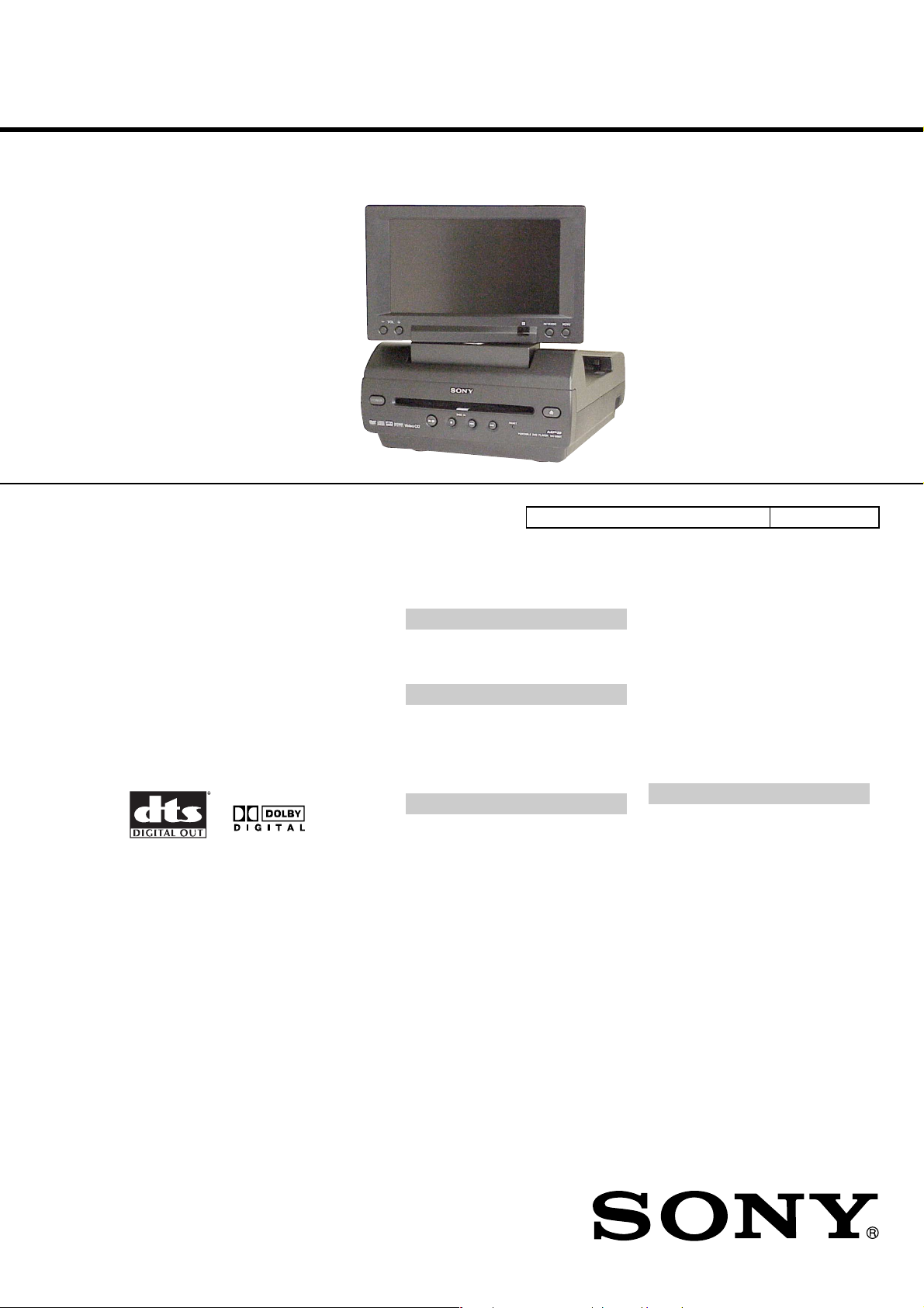
PORTABLE DVD PLAYER
MV-65ST
About discs this player can
play
This player can play the following discs:
• DVD
• DVD-R
• DVD-RW
• Video CD
• Audio CD
• CD-R/CD-RW
Disc type Label on the disc
DVD Videos
Video CDs
Audio CDs
MP3 files/
JPEG files
“DVD VIDEO,” “DVD-R” and “DVD-RW” are
trademarks.
W
CAUTION
Use of controls or adjustments or performance of procedures
other than those specified herein may result in hazardous radiation exposure.
Notes on chip component replacement
• Never reuse a disconnected chip component.
• Notice that the minus side of a tantalum capacitor may be dam-
aged by heat.
Flexible Circuit Board Repairing
• Keep the temperature of the soldering iron around 270 °C during repairing.
• Do not touch the soldering iron on the same conductor of the
circuit board (within 3 times).
• Be careful not to apply force on the conductor when soldering
or unsoldering.
This label is located on the bottom of the
chassis.
CAUTION INVISIBLE
VIEW DIRECTLY WITH OPTICAL INSTRUMENTS
This label is located on the drive unit’s internal
chassis.
On power sources
• Use house current or car battery (12 V DC).
• For use in your house, use the AC power
adaptor supplied with the player. Do not use
any other AC power adaptor since it may
cause the player to malfunction.
Polarity of
the plug
LASER RADIATION WHEN OPEN
DO NOT STARE INTO BEAM OR
Notes on CD-Rs (recordable CDs)/
CD-RWs (rewritable CDs)
• Some CD-Rs/CD-RWs (depending on the
equipment used for its recording or the
condition of the disc) may not play on this
player.
• You cannot play a CD-R/CD-RW that is not
finalized*.
• You cannot play a CD-R/CD-RW that is
recorded in Multi Session.
• You can play MP3/JPEG files recorded on
CD-ROMs, CD-Rs, and CD-RWs.
* A process necessary for a recorded CD-R/CD-R
disc to be played on the audio CD player.
SAFETY-RELATED COMPONENT WARNING!!
COMPONENTS IDENTIFIED BY MARK 0 OR DOTTED
LINE WITH MARK 0 ON THE SCHEMATIC DIAGRAMS
AND IN THE PARTS LIST ARE CRITICAL TO SAFE
OPERATION. REPLACE THESE COMPONENTS WITH
SONY PARTS WHOSE PART NUMBERS APPEAR AS
SHOWN IN THIS MANU AL OR IN SUPPLEMENTS PUBLISHED BY SONY.
2
ATTENTION AU COMPOSANT AYANT RAPPORT
À LA SÉCURITÉ!
LES COMPOSANTS IDENTIFIÉS P AR UNE MARQUE 0
SUR LES DIAGRAMMES SCHÉMATIQUES ET LA LISTE
DES PIÈCES SONT CRITIQUES POUR LA SÉCURITÉ
DE FONCTIONNEMENT. NE REMPLACER CES COMPOSANTS QUE PAR DES PIÈCES SONY DONT LES
NUMÉROS SONT DONNÉS DANS CE MANUEL OU
DANS LES SUPPLÉMENTS PUBLIÉS PAR SONY.
SECTION 1
SERVICING NOTES
MV-65ST
TABLE OF CONTENTS
1. SERVICING NOTES ............................................... 3
2. GENERAL
Location of Controls ....................................................... 4
3. DISASSEMBLY
3-1. Disassembly Flow ........................................................... 7
3-2. Base (Monitor) Assy ....................................................... 8
3-3. Cabinet (Front) Assy ....................................................... 8
3-4. Monitor Assy ................................................................... 9
3-5. Hinge ............................................................................... 10
3-6. MONITOR Board ........................................................... 10
3-7. Liquid Crystal Display Panel (LCD1)............................ 11
3-8. DVD MD Assy ................................................................ 11
3-9. SERVO Board, Mechanism Deck................................... 12
3-10. TD-S-Top-Cover ............................................................. 12
3-11. Loading Mechanism Assy............................................... 13
3-12. Traverse Mechanism Assy .............................................. 13
4. TEST MODE.............................................................. 14
5. ELECTRICAL ADJUSTMENTS......................... 15
6. DIAGRAMS
6-1. Block Diagram – AUDIO Section – ............................... 18
6-2. Block Diagram – VIDEO, PANEL Section –................ 19
6-3. Block Diagram – POWER Section –.............................. 20
6-4. Note for Printed Wiring Boards
and Schematic Diagrams ................................................ 21
6-5. Printed Wiring Board
– MONITOR Board (Side A) – ...................................... 22
6-6. Printed Wiring Board
– MONITOR Board (Side B) – ...................................... 23
6-7. Schematic Diagram – MONITOR Board (1/4) – ........... 24
6-8. Schematic Diagram – MONITOR Board (2/4) – ........... 25
6-9. Schematic Diagram – MONITOR Board (3/4) – ........... 26
6-10. Schematic Diagram – MONITOR Board (4/4) – ........... 27
6-11. Printed Wiring Board – KEY Board –............................ 28
6-12. Schematic Diagram – KEY Board – .............................. 29
6-13. Schematic Diagram – POWER Section (1/2) –.............. 30
6-14. Schematic Diagram – POWER Section (2/2) –.............. 31
6-15. Printed Wiring Board – POWER Board (Side A) – ....... 32
6-16. Printed Wiring Board – POWER Board (Side B) – ....... 33
6-17. Printed Wiring Board – AMP Section – ......................... 34
7. EXPLODED VIEWS
7-1. Overall Section................................................................ 46
7-2. Cabinet (Front) Section................................................... 47
7-3. Base (Monitor) Section ................................................... 48
7-4. Monitor Section............................................................... 49
7-5. Cabinet (Lower) Section-1.............................................. 50
7-6. Cabinet (Lower) Section-2.............................................. 51
7-7. Mechanism Deck Section-1 ............................................ 52
7-8. Mechanism Deck Section-2 ............................................ 53
7-9. Mechanism Deck Section-3 ............................................ 54
8. ELECTRICAL PARTS LIST ............................ 55
NOTES ON HANDLING THE OPTICAL PICK-UP
BLOCK OR BASE UNIT
The laser diode in the optical pick-up block may suffer electrostatic break-down because of the potential difference generated
by the charged electrostatic load, etc. on clothing and the human
body.
During repair, pay attention to electrostatic break-down and also
use the procedure in the printed matter which is included in the
repair parts.
The flexible board is easily damaged and should be handled with
care.
NOTES ON LASER DIODE EMISSION CHECK
Never look into the laser diode emission from right above when
checking it for adjustment. It is feared that you will lose your sight.
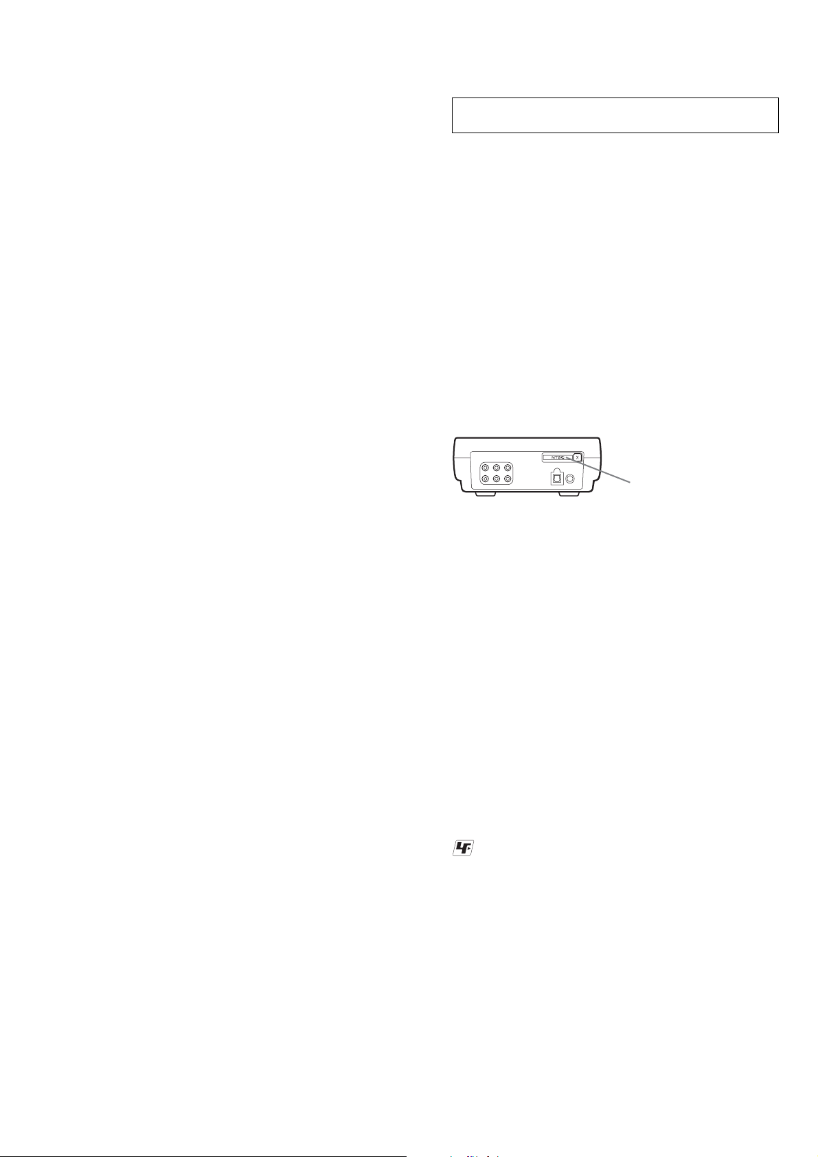
For E model NTSC type and PAL type.
The type of an NTSC system and the type of a P AL system exist in
E model.
Please refer to the following figure about how to recognize.
– BACK VIEW –
NTSC: NTSC TYPE
PAL: PAL TYPE
UNLEADED SOLDER
Boards requiring use of unleaded solder are printed with the leadfree mark (LF) indicating the solder contains no lead.
(Caution: Some printed circuit boards may not come printed with
the lead free mark due to their particular size)
: LEAD FREE MARK
Unleaded solder has the following characteristics.
• Unleaded solder melts at a temperature about 40 °C higher than
ordinary solder.
Ordinary soldering irons can be used but the iron tip has to be
applied to the solder joint for a slightly longer time.
Soldering irons using a temperature regulator should be set to
about 350 °C.
Caution: The printed pattern (copper foil) may peel away if the
heated tip is applied for too long, so be careful!
• Strong viscosity
Unleaded solder is more viscou-s (sticky, less prone to flow)
than ordinary solder so use caution not to let solder bridges occur such as on IC pins, etc.
• Usable with ordinary solder
It is best to use only unleaded solder but unleaded solder may
also be added to ordinary solder.
3

MV-65ST
Location of controls
MV-65ST
6
SECTION 2
GENERAL
D
IS
C
I
N
R
E
E
S
T
This section is extracted from
instruction manual.
9
0
qa
qs
qd
7
8
Refer to the pages listed for details.
1 Monitor
2 VOL −/+ buttons
To turn up or down the volume or to select
the item during menu operation.
3 Disc slot
4 DISC IN light
When a disc is in the player, the DISC IN
light glows orange.
5 POWER (on/off) button
To turn on/off the player.
6 u (play/pause) button
7 x (stop) button
8 . (previous)/> (next) buttons
9 Receptor for the card remote
commander
q; Reverse button
To switch images upside down and
reverse the output of the audio channels.
qf
qg
qa Speakers (left/right)
qs MENU button
To make various display settings and FM
transmitter setting.
qd HEADPHONES jacks
To connect the headphones. 2 sets of
headphones can be connected.
qf Z (eject) button
Available to eject a disc from the player
even when the player is turned off.
qg RESET button
Note
Even when the player is turned off by pressing
(POWER), you can eject a disc from the player,
though you cannot insert a disc.
4
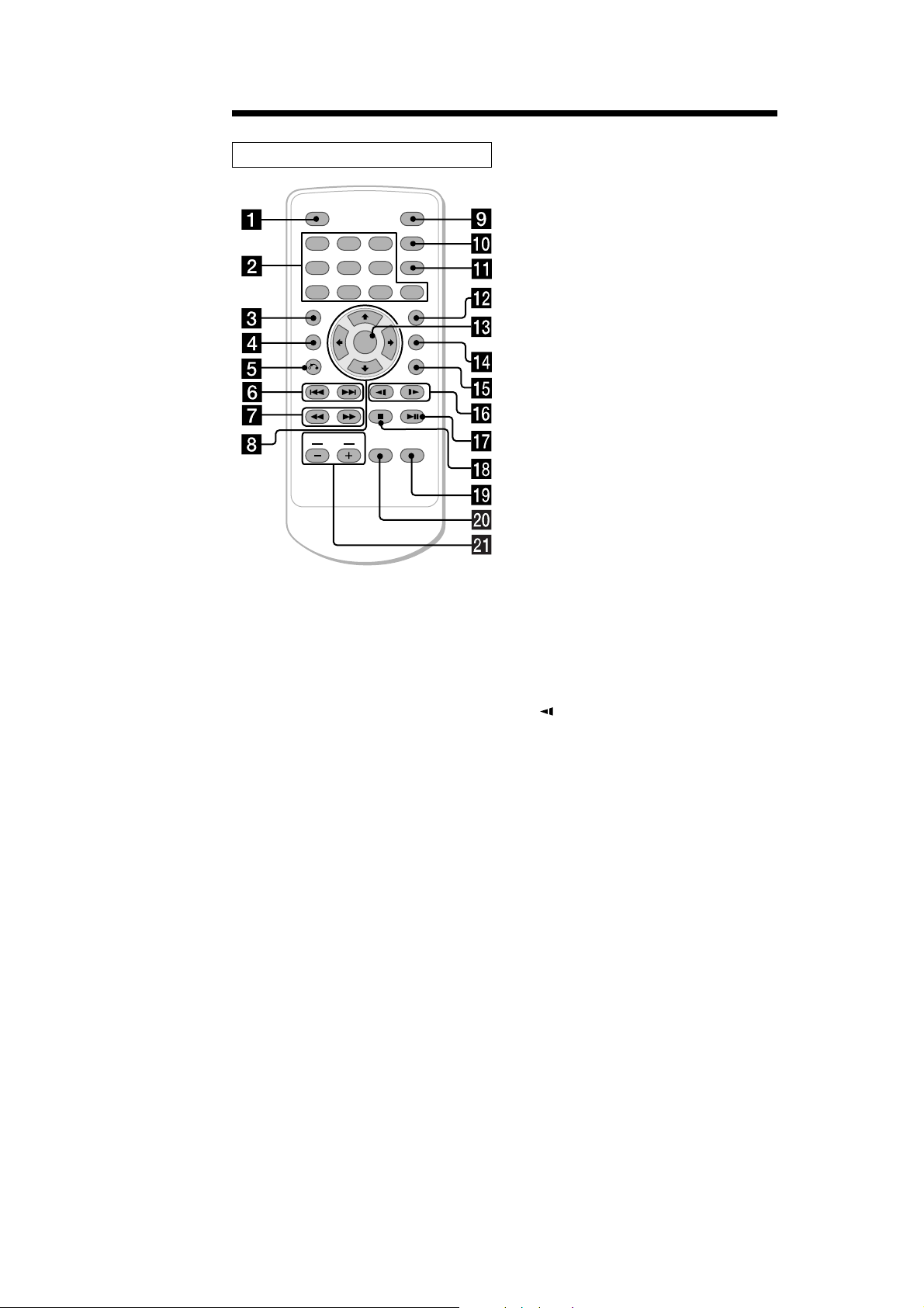
Card remote commander RM-X137
ENTER
INPUT
POWER
SEARCH
CLEAR
SUBTITLE
ANGLE
AUDIO
SETUP
DISPLAY
123
456
7 890
TOP MENU
MENU
VOL
The corresponding buttons of the card
remote commander control the same
functions as those on the player.
Instructions in this manual describe how to use
the player by mainly using the card remote
commander.
Tip
Refer to “Replacing the lithium battery of the card
remote commander” for details on how to replace
the battery.
MV-65ST
Refer to the pages listed for details.
1 DISPLAY button
To display the time information of the disc.
2 Number buttons (0 to 9)
3 TOP MENU button
To display the top menu of a recorded
DVD.
4 MENU button
To display the recorded DVD menu, or to
turn on/off the PBC (Playback control)
menu of a Video CD.
5 O (return) button
6 ./> (previous/next) buttons
7 m (fast reverse)/
M (fast forward) buttons
8 M/,/m/< buttons
9 POWER (on/off) button
To turn on/off the player.
q; SEARCH button
To specify a desired point on a disc by
chapter, title, or track.
qa CLEAR button
qs SUBTITLE button
To change the subtitle language while
playing a DVD.
qd ENTER button
To enter a setting.
qf ANGLE button
To select the multiple angles of view while
playing a DVD.
qg AUDIO button
To change the audio output/audio
language.
qh
(slow reverse)/y (slow forward)
buttons
qj u (play/pause) button
qk x (stop) button
ql SETUP buttons
Used to perform menu operations.
w; INPUT button
To select the input source.
wa VOL (−/+) buttons
To turn up or down the volume.
5
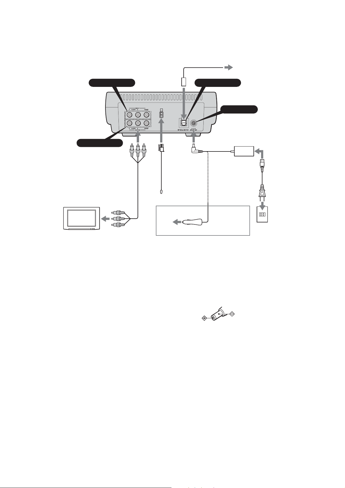
MV-65ST
This player is supplied with two types of
power cable. When you use the player in the
car, connect the player to the cigar lighter
socket; when using at home, connect it to the
AC outlet.
AUDIO/VIDEO INPUT OPTICAL OUTPUT
Two headphones
connectors
(at the side)
AUDIO/VIDEO OUTPUT
Audio/video
cable
(not supplied)
TV, etc.
Antenna for FM
transmission
(supplied)
(US, Canadian
Mexican only)
Optical cable
(not supplied)
AC power
adaptor
(supplied)
*
Power cord for the
cigar lighter socket
DC IN 12V
AC power cord
(supplied)
(supplied)
When using the
player in the car
To a digital
amplifier, etc.
To audio/video
input connectors
On AUDIO/VIDEO OUTPUT
connectors
Yo u can connect a TV to the AUDIO/VIDEO
OUTPUT connectors to output the contents
being played back on the player. Connect the
yellow plugs of the audio/video cable to the
video connectors on both the TV and the
player and connect the white plugs and the red
plugs to the white (left audio) connectors and
red (right audio) connectors respectively.
On AUDIO/VIDEO INPUT connectors
Yo u can connect a VTR, etc. to the AUDIO/
VIDEO INPUT connectors to input the
contents being played back on the device. You
can connect the device in the same way as
described on “On AUDIO/VIDEO OUTPUT
connectors” above.
To the cigar lighter socket
Notes
• When connecting the other device to the player,
be sure to connect the player to the power
source after all other connections are completed.
• If an obstacle such as cigar ash is caught inside
the cigar lighter socket, the contact between the
power cord plug and the socket becomes
incomplete and the plug may get extremely hot
during use. To avoid this, check the socket and
clean it if necessary before connecting the power
cord.
* Polarity of the plug
To a
wall
outlet
6
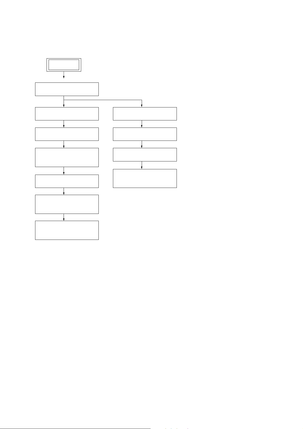
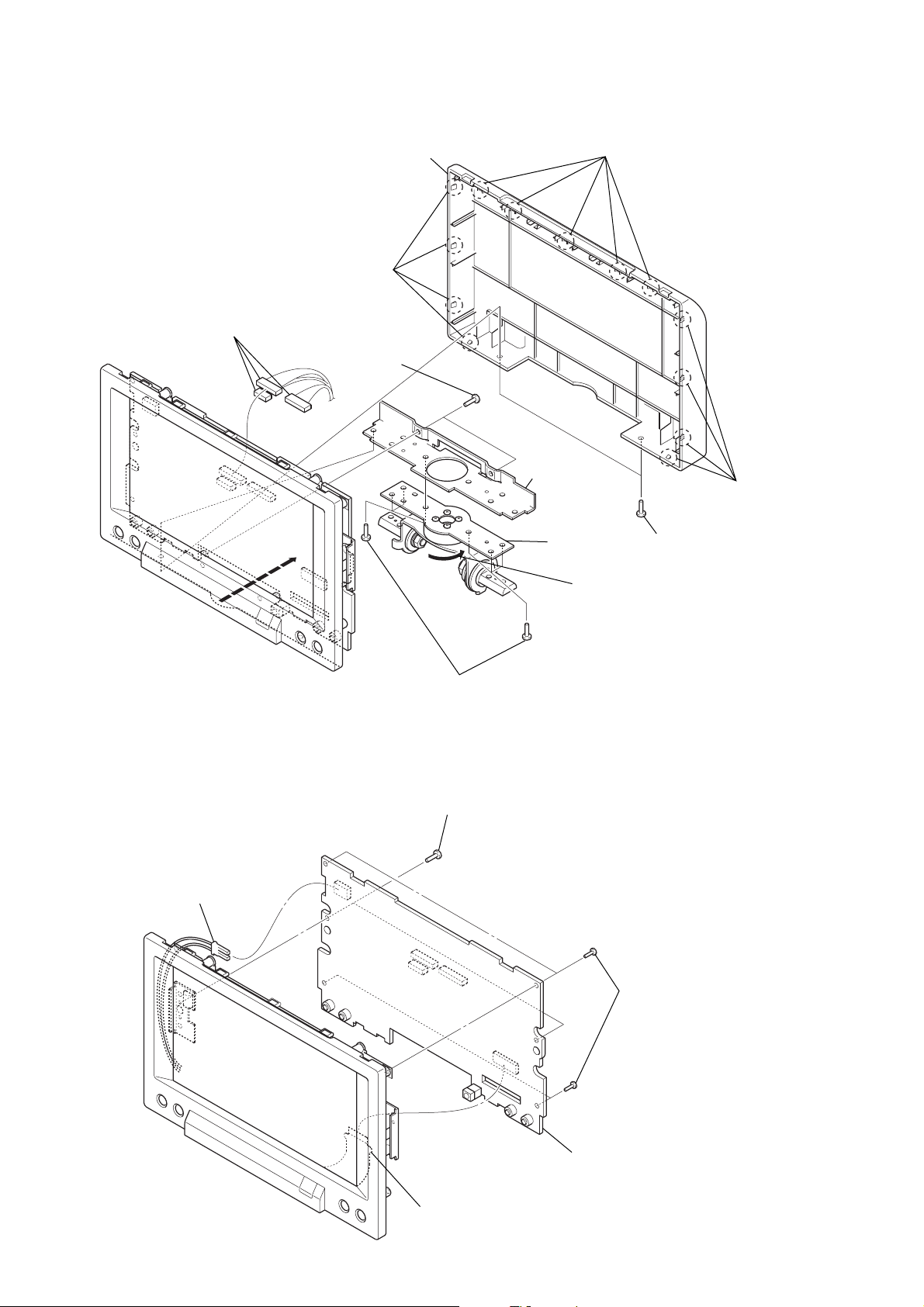
• This set can be disassembled in the order shown below.
3-1. DISASSEMBLY FLOW
SET
3-2. BASE (MONITOR) ASSY
(Page 8)
MV-65ST
SECTION 3
DISASSEMBLY
3-3. CABINET (FRONT) ASSY
(Page 8)
3-8. DVD MD ASSY
(Page 11)
3-9. SERVO BOARD,
MECHANISM DECK
(Page 12)
3-10. TD-S-TOP-COVER
(Page 12)
3-11. LOADING MECHANISM
ASSY
(Page 13)
3-12. TRAVERSE MECHANISM
ASSY
(Page 13)
3-4. MONITOR ASSY
(Page 9)
3-5. HINGE
(Page 10)
3-6. MONITOR BOARD
(Page 10)
3-7. LIQUID CRYSTAL
DISPLAY PANEL (LCD1)
(Page 11)
7
MV-65ST
y
Note: Follow the disassembly procedure in the numerical order given.
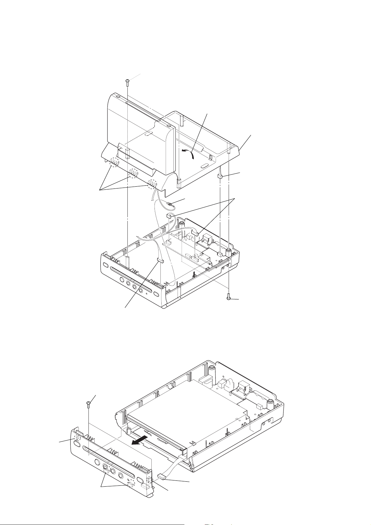
3-2. BASE (MONITOR) ASSY
3
two screws
(BVTP3
4
three claws
×
12)
5
2
terminal
Open the monitor
6
6
two connectors
(CN901, CN902)
7
base (monitor) ass
connector
(CN371)
6
3-3. CABINET (FRONT) ASSY
1
two screws
(BTP2.6 × 8)
2
claw
connector
(CN701)
3
1
two screws
(BVTP3
×
12)
4
2
two claws
2
claw
connector
(CN702)
8
3-4. MONITOR ASSY
3
two claws
4
front cover (hinge)
2
two screws
(P2 × 8)
1
Open the monitor.
MV-65ST
7
four screws
(PS3
×
10)
6
rear cover (hinge)
8
monitor assy
5
Close the monitor.
9
MV-65ST
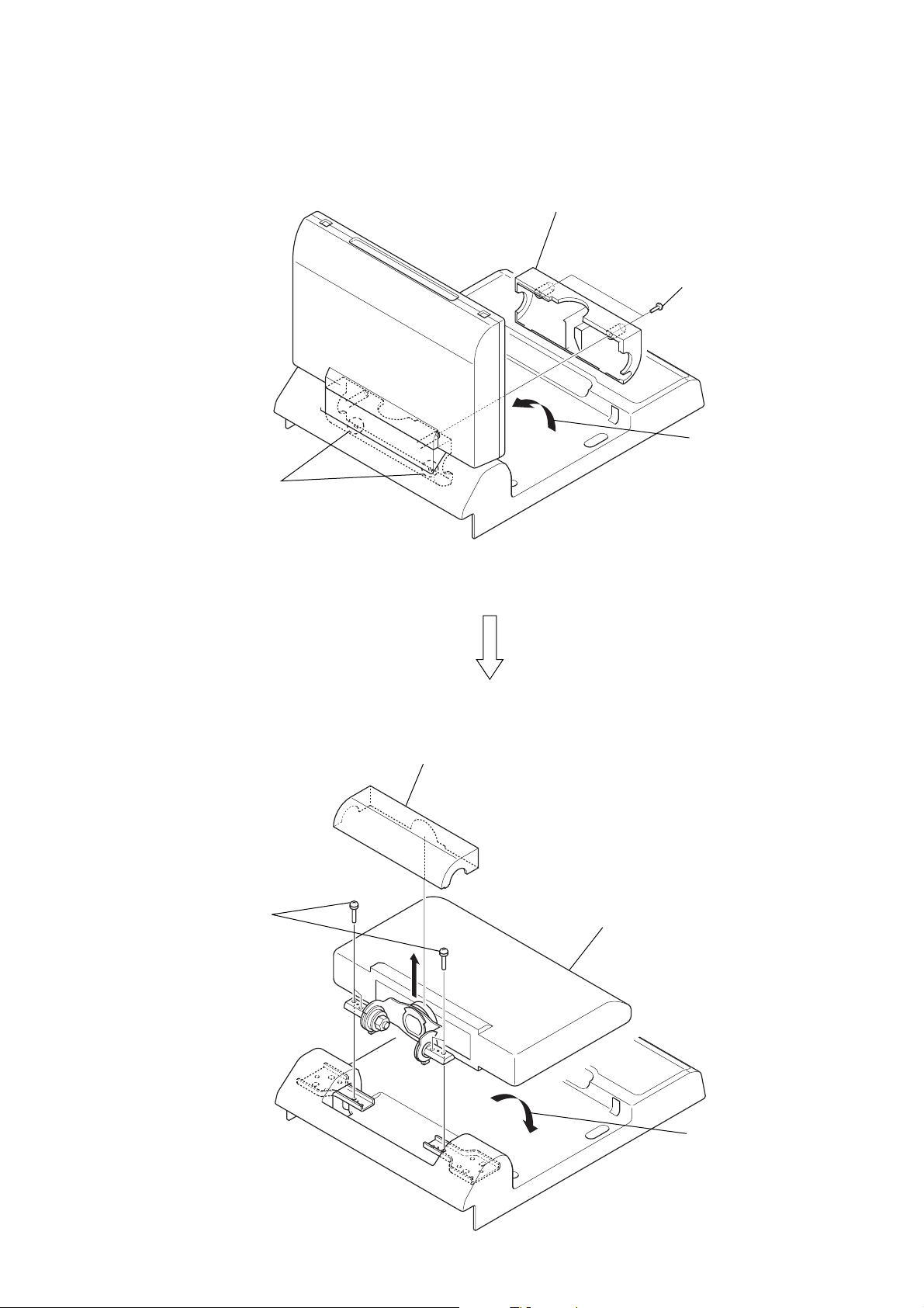
s
s
3-5. HINGE
three connectors
4
(CN904, CN905, CN906)
3
rear case (LCD)
2
four claws
5
two screws
(P2 × 8)
9
LCD bracket
hinge
2
five claws
2
four claw
3-6. MONITOR BOARD
2
connector
(CN850)
6
8
six screws
(B2.6 × 4)
4
two screws
(B2 × 5)
3
four screw
(P2 × 8)
1
q;
hinge
7
It is half rotation about a hinge.
two screws
(B2 × 5)
10
1
LCD flexible board
(CN801)
5
MONITOR board
MV-65ST
s
)
3-7. LIQUID CRYSTAL DISPLAY PANEL (LCD1)
6
two retainers (LCD)
2
bracket (LCD)
1
8
sheet (insulating)
9
liquid crystal display panel (LCD1)
two screws
(BTP2 × 6)
5
four screws
(BTP2 × 6)
6
two retainers (LCD)
7
insulating sheet (B)
3
4
bracket (LCD)
two screw
(BTP2 × 6)
3-8. DVD MD ASSY
2
top case (shield)
3
5
1
three screws
(B2.6
two screws
(BVTP3
DVD MD assy
×
×
12)
6)
q;
front case (LCD) assy
1
three screws
(B2.6
×
6)
4
three screws
(CN302, CN303, CN903
3
two screws
(BVTP3
×
12)
11
MV-65ST
)
3-9. SERVO BOARD, MECHANISM DECK
6
mechanism deck
2
wire (flat type)
(CN401)
1
FFC-0.5-24 core L70
(CN301)
5
SERVO board
3
two screws
(B2.6
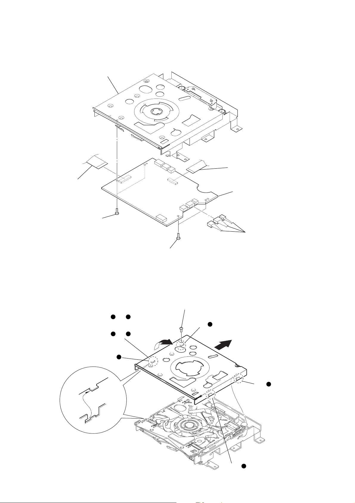
3-10. TD-S-TOP-COVER
2
Slide the TD-S-top-cover
in the direction of arrow
then disengage the claw and .
Hold up the TD-S-top-cover
in the direction of arrow
then disengage the claw and .
×
6)
4
three connectors
(J401, J402, J403
3
two screws
×
6)
(B2.6
1
A
B
claw
,
a
b
,
c
d
a
B
screw
(PTT2
claw
×
4)
b
A
d
claw
12
claw
c
3-11. LOADING MECHANISM ASSY
)
s
2
loading mechanism assy
1
screw
(PTT2
MV-65ST
×
4
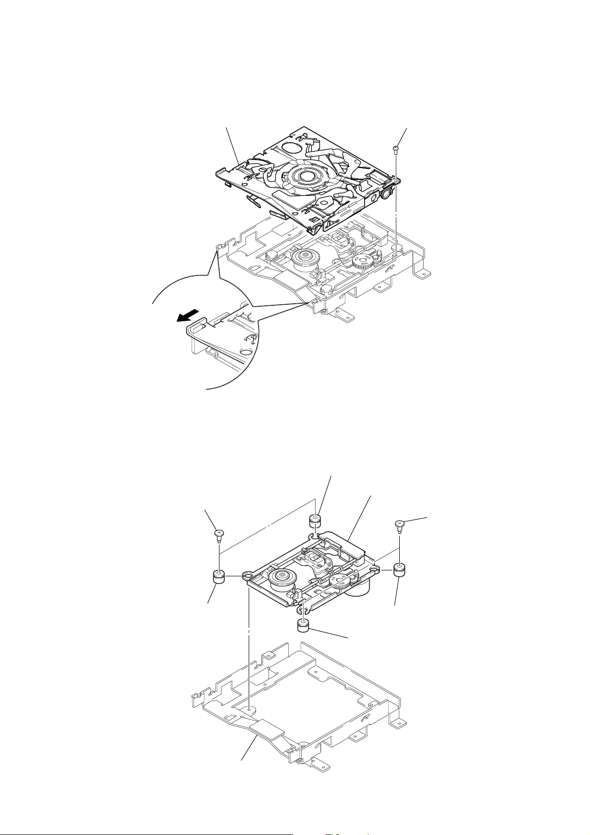
3-12. TREVERSE MECHANISM ASSY
1
two SCW-dampers
4
damper idle
7
damper idle
5
8
traverse mechanism assy
6
damper idle
damper idle
2
two SCW-damper
3
AS-main-base
13
MV-65ST
SECTION 4
TEST MODE
Note: This set is able to setting the adjustment data, reset to factory de-
fault and initialize the EEPROM (IC402 on the MONITOR board)
in the test mode.
ENTER THE TEST MODE
Procedure:
1. Press the [POWER] button to turn the power on.
2. While pressing the [VOL --] and . buttons, press the [RE-
SET] button.
3. The set is enter the test mode and display as bellow figure.
Display
MV-65ST TEST MODE MENU
1. NTSC/PAL SELECT
2. FOR FACTORY
3. LCD SETTING
4. FM TRANSMITTER
5. HEAT PROTECTION
6. LOAD DEFAULT
7. SOFT RESET(EXIT)
Ver.20XX-XX-XX
Note: If initial data is not written to the EEPROM (IC402 on the MONI-
TOR board) or data is clobbered, the set is not able to display normally screen.
BATCH WRITING OF THE INITIAL DATA TO
EEPROM
In the test mode, by pressing the [VOL --] button at two seconds,
batch writing is possible of the initial data to EEPOM (IC402 on
the MONITOR board).
3. LCD SETTING
This mode is not used in servicing.
4. FM TRANSMITTER
In this mode, switch the frequency range of FM transmitter as
follow.
1) USA (88.3 to 89.9 MHz)
2) Japan (76.5 to 79.5 MHz)
3) Transmitter off
5. HEAT PROTECTION
This mode is not used in servicing.
6. LOAD DEFAULT
This mode is not used in servicing.
7. SOFT RESET (EXIT)
Releasing the test mode.
OPERATION OF THE TEST MODE
All operations are performed using the bellow buttons.
Button Function
MENU Select the item
REVERSE Enter
VOL + Up the data value
VOL − Down the data value
RELEASING THE TEST MODE
In the test mode menu screen, press the [MENU] button to select
“7. SOFT RESET (EXIT)”, and press the [REVERSE] button to
release the test mode.
OPERATING THE EACH ITEM
1. NTSC/PAL SELECT
In this mode, switch the signal format system to NTSC or P AL.
2. FOR FACTORY
In this mode, change the data of adjustment data.
Enter this mode, it displays each adjustment item as follow.
1) Com Gain
2) Y Gain
3) Black Limit
4) White Limit
5) R-Sub BRT
6) B-Sub BRT
7) R-Sub CONT
8) B-Sub CONT
9) Gamma 1
10) Gamma 2
11) VCO Free Run
12) PLL/V Pos
13) H Pos
14
SECTION 5
r
r
r
r
r
r
ELECTRICAL ADJUSTMENTS
MV-65ST
1. DC/DC CONVERTER ADJUSTMENT
1-1. Frequency Adjustment
Setting:
oscilloscope
or
frequency counte
MONITOR board
TP802
TP804
Procedure:
1. Connect an oscilloscope or frequency counter to the TP802
and TP804 on the MONITOR board.
2. Check that the voltage between TP951 (−) and TP952 (+) is
14.4 V. Press the [POWER] button to turn the power on.
3. Adjust the RV801 on the MONITOR board so that the value
of oscilloscope or frequency counter becomes 243 kHz ±3 kHz.
1-2. 5V V oltage Adjustment
Setting:
MONITOR board
TP807
TP804
Procedure:
1. Connect a digital voltmeter to the TP804 and TP807 on the
MONITOR board.
2. Check that the voltage between TP951 (−) and TP952 (+) is
14.4 V. Press the [POWER] button to turn the power on.
3. Adjust the RV803 on the MONITOR board so that the value
of digital voltmeter becomes 5.05 V ±0.03 V .
1-3. Other V oltages Check
Setting:
MONITOR board
TP805/TP806/TP808
TP804
Procedure:
− Vdd V oltage Check −
1. Connect a digital voltmeter to the TP804 and TP808 on the
MONITOR board.
2. Check that the voltage between TP951 (−) and TP952 (+) is
14.4 V. Press the [POWER] button to turn the power on.
3. Check that the value of digital voltmeter is 3.45 V ±0.2 V .
− Vgh V oltage Check −
4. Connect the digital voltmeter to the TP804 and TP806 on the
MONITOR board.
5. Check that the value of digital voltmeter is 17.5 V ±1.5 V .
− Vss V oltage Check −
6. Connect the digital voltmeter to the TP804 and TP805 on the
MONITOR board.
7. Check that the value of digital voltmeter is –12.0 V ±1.5 V.
+
–
digital voltmete
+
–
digital voltmete
+
–
2. PLL ADJUSTMENT
Setting:
digital voltmete
MONITOR board
TP601
TP602
+
–
Procedure:
1. Connect a digital voltmeter to the TP601 and TP602 on the
MONITOR board.
2. Check that the voltage between TP951 (−) and TP952 (+) is
14.4 V. Press the [POWER] button to turn the power on.
3. Adjust the RV601 on the MONITOR board so that the value
of digital voltmeter becomes 2.5 V ±0.15 V .
3. INVERTER HIGH VOLTAGE CHECK
Setting:
digital voltmete
MONITOR board
TP853
TP854
+
–
Procedure:
− High Voltage Check −
1. Connect a digital voltmeter (for withstand high voltage) to the
TP853 and TP854 on the MONITOR board.
2. Check that the voltage between TP951 (−) and TP952 (+) is
14.4 V. Press the [POWER] button to turn the power on.
(DIMMER: off)
3. Check that the value of digital voltmeter is 550 V ±150 V (rms).
− Frequency Check −
4. Connect an oscilloscope (use a probe for withstand high voltage) to the TP853 and TP854 on the MONITOR board.
5. Check that the frequency of oscilloscope is 66 kHz ±2.5 kHz.
4. OSD DOT CLOCK CHECK
Setting:
frequency counte
MONITOR board
TP403
TP405
Procedure:
1. Connect a frequency counter (high impedance) to the TP403
and TP405 on the MONITOR board.
2. Check that the voltage between TP951 (−) and TP952 (+) is
14.4 V. Press the [POWER] button to turn the power on.
3. Check that the value of frequency counter is 6.5 MHz ±0.2
MHz.
+
–
15
MV-65ST
r
r
e
V
V
+
–
oscilloscope
MONITOR board
TP811
TP513
5. NTSC SUB CARRIER CHECK
Setting:
frequency counte
MONITOR board
TP510
TP513
+
–
Procedure:
1. Connect a frequency counter (high impedance) to the TP510
and TP513 on the MONITOR board.
2. Check that the voltage between TP951 (−) and TP952 (+) is
14.4 V. Press the [POWER] button to turn the power on.
3. Set the signal format system to NTSC. (refer to “4. TEST
MODE”)
4. Check that the value of frequency counter is 3.579545 MHz
±100 Hz.
6. PAL SUB CARRIER CHECK
Setting:
frequency counte
MONITOR board
TP510
TP513
Procedure:
1. Connect a frequency counter (high impedance) to the TP510
and TP513 on the MONITOR board.
2. Check that the voltage between TP951 (−) and TP952 (+) is
14.4 V. Press the [POWER] button to turn the power on.
3. Set the signal format system to PAL. (refer to “4. TEST
MODE”)
4. Check that the value of frequency counter is 4.433619 MHz
±100 Hz.
+
–
− Waveform Position Set-up Adjustment −
7. Adjust the RV802 on the MONITOR boar d so that A value of
waveform becomes −2.1 V ±0.1 V.
4.9 V ± 0.1 V
0 V
A
: – 2.1 V ± 0.1
8. VIDEO ADJUSTMENT
Note: Perform the following adjustment items in test mode.
Common Setting:
1. Check that the voltage between TP951 (−) and TP952 (+) is
14.4 V. Press the [POWER] button to turn the power on.
2. Enter the test mode, and enter the “2. FOR FA CTORY” mode.
(refer to “4. TEST MODE”)
3. Set the signal format system to NTSC. (refer to “4. TEST
MODE”)
4. Input 10 steps signal (NTSC, without burst) to the VIDEO
INPUT jack (J301 on the POWER board) from pattern generator.
Waveform of input signal
1 Vp-p
0.286 V
fig. 8-1
Waveform of output signal
(TP810, TP811, TP812)
7. V-COM ADJUSTMENT
Setting:
oscilloscop
MONITOR board
TP819
TP828
Procedure:
− Voltage Set-up Adjustment −
1. Connect an oscilloscope to the TP819 and TP828 on the MONITOR board.
2. Check that the voltage between TP951 (−) and TP952 (+) is
14.4 V. Press the [POWER] button to turn the power on.
3. Enter the test mode, and enter the “2. FOR FA CTORY” mode.
(refer to “4. TEST MODE”)
4. Press the [MENU] button to display “Com Gain”, and press the
[REVERSE] button.
5. Adjust by pressing the [+]/ − buttons so that the voltage of
oscilloscope becomes 7.0 Vp-p ±0.1 V.
7.0 Vp-p ± 0.1
6. Press the [REVERSE] button and write the date to EEPROM
(IC402 on the MONITOR board).
+
–
0 V
AB CDE
fig. 8-2
1 Contrast Level of Luminance Signal
Setting:
Procedure:
1. Connect an oscilloscope to the TP513 and TP811 on the MONITOR board.
2. Press the [MENU] button to display “Y Gain”, and press the
[REVERSE] button.
3. Adjust by pressing the [+]/
− buttons so that the D value of
waveform (fig. 8-2) becomes 3.4 V ±0.1 V.
4. Press the [REVERSE] button and write the date to EEPROM
(IC402 on the MONITOR board).
16
MV-65ST
r
2 Back Limiter Level
Procedure:
1. In the “1 Contrast Level of Luminance Signal” status, press
the [MENU] utton to display “Black Limit”, and press the [RE-
VERSE] button.
2. Adjust by pressing the [+]/ − buttons so that the A value of
waveform (fig. 8-2) becomes 1.0 V ±0.1 V.
3. Press the [REVERSE] button and write the date to EEPROM
(IC402 on the MONITOR board).
3 White Limiter Level
Procedure:
1. In the “2 Black Limiter Level” status, press the [MENU] but-
ton to display “White Limit”, and press the [REVERSE] but-
ton.
2. Adjust by pressing the [+]/ − buttons so that the E value of
waveform (fig. 8-2) becomes 3.9 V ±0.1 V.
3. Press the [REVERSE] button and write the date to EEPROM
(IC402 on the MONITOR board).
4 R-sub Bright
Procedure:
1. In the “3 White Limiter Level” status, connect the oscillo-
scope to the TP513 and TP810 on the MONITOR board.
2. Press the [MENU] button to display “R-Sub BRT”, and press
the [REVERSE] button.
3. Adjust by pressing the [+]/ − buttons so that the A value of
waveform (fig. 8-2) becomes 1.0 V ±0.1 V.
4. Press the [REVERSE] button and write the date to EEPROM
(IC402 on the MONITOR board).
5 B-sub Bright
Procedure:
1. In the “4 R-sub Bright” status, connect the oscilloscope to
the TP513 and TP812 on the MONITOR board.
2. Press the [MENU] button to display “B-Sub BRT”, and press
the [REVERSE] button.
3. Adjust by pressing the [+]/
− buttons so that the A value of
waveform (fig. 8-2) becomes 1.0 V ±0.1 V.
4. Press the [REVERSE] button and write the date to EEPROM
(IC402 on the MONITOR board).
6 R-ch Sub Contrast
Procedure:
1. In the “5 B-sub Bright” status, connect the oscilloscope to
the TP513 and TP810 on the MONITOR board.
2. Press the [MENU] button to display “R-Sub CONT”, and press
the [REVERSE] button.
3. Adjust by pressing the [+]/ − buttons so that the D value of
waveform (fig. 8-2) becomes 3.4 V ±0.1 V.
4. Press the [REVERSE] button and write the date to EEPROM
(IC402 on the MONITOR board).
7 B-ch Sub Contrast
Procedure:
1. In the “6 R-ch Sub Contrast” status, connect the oscilloscope
to the TP513 and TP812 on the MONITOR board.
2. Press the [MENU] button to display “B-Sub CONT”, and press
the [REVERSE] button.
3. Adjust by pressing the [+]/ − buttons so that the D value of
waveform (fig. 8-2) becomes 3.4 V ±0.1 V.
4. Press the [REVERSE] button and write the date to EEPROM
(IC402 on the MONITOR board).
8 Gamma 1
Procedure:
1. In the “7 B-ch Sub Contrast” status, connect the oscilloscope
to the TP513 and TP811 on the MONITOR board.
2. Press the [MENU] button to display “Gamma 1”, and press the
[REVERSE] button.
3. Adjust by pressing the [+]/ − buttons so that the B value of
waveform (fig. 8-2) becomes 2.0 V ±0.1 V.
4. Press the [REVERSE] button and write the date to EEPROM
(IC402 on the MONITOR board).
9 Gamma 2
Procedure:
1. In the “8 Gamma 1” status, press the [MENU] button to dis-
play “Gamma 2”, and press the [REVERSE] button.
2. Adjust by pressing the [+]/ − buttons so that the C value of
waveform (fig. 8-2) becomes 3.2 V ±0.1 V.
3. Press the [REVERSE] button and write the date to EEPROM
(IC402 on the MONITOR board).
q; VCO Free Run
Setting:
frequency counte
MONITOR board
TP506
TP513
+
–
Procedure:
1. In the “9 Gamma 2” status, connect a frequency counter to
the TP506 and TP513 on the MONITOR board.
2. Press the [MENU] button to display “VCO Free Run”, and press
the [REVERSE] button.
3. Adjust by pressing the [+]/
− buttons so that the value of fre-
quency counter becomes 15.734 kHz ±50 Hz.
4. Confirm that the displayed screen is normally display.
5. Press the [REVERSE] button and write the date to EEPROM
(IC402 on the MONITOR board).
qa Vertical Position
Procedure:
1. In the “q; VCO Free Run” status, input the monoscope signal
to the VIDEO INPUT jack (J301 on the POWER board).
2. Press the [MENU] button to display “PLL/V Pos”, and press
the [REVERSE] button.
3. Adjust by pressing the [+]/ − buttons so that the vertical posi-
tion of screen on the monitor becomes the most suitable.
4. Press the [REVERSE] button and write the date to EEPROM
(IC402 on the MONITOR board).
qs Horizontal Position
Procedure:
1. In the “qa Vertical Position” status, press the [MENU] button
to display “H Pos”, and press the [REVERSE] button.
2. Adjust by pressing the [+]/ − buttons so that the horizontal
position of screen on the monitor becomes the most suitable.
3. Press the [REVERSE] button and write the date to EEPROM
(IC402 on the MONITOR board).
Adjustment Location:
– MONITOR BOARD (SIDE A) –
RV601
RV802
– MONITOR BOARD (SIDE B) –
TP853
TP854
TP802
TP952 (+)
TP951 (
−
)
TP808
TP807
RV803
TP954
TP953
RV801
TP804
TP805
TP806
TP403
TP602
TP405
TP601
TP819
TP513
TP510
TP810
TP811
TP812
TP506
TP828
1717

MV-65ST
SECTION 6
DIAGRAMS
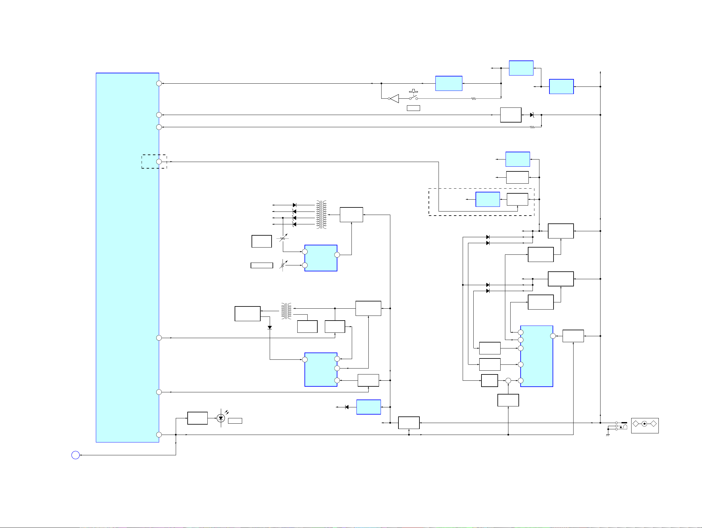
6-1. BLOCK DIAGRAM – AUDIO Section –
J301 (1/2)
VIDEO
R-CH
DIFFERENTIAL
R-CH
AMP
IC301
INPUT
OPTICAL
OUTPUT
L
AUDIO
R
OPTICAL
TRANSCEIVER
DVD MECHANISM
DECK BLOCK
AUDIO-DL
AUDIO-DR
J302
SPDIF
CVBS
VIDEO/AUDIO SELECT
IC302
3 VIN1
8 LIN1
1
7 LIN2
VOUT2
VIN2
SW22SW1
9
CVBS
J301 (2/2)
VIDEO
BUFFER AMP
IC305
R-CH
MUTING
Q102
R-CH
(US, Canadian, Mexican)
15
11LOUT2
14VOUT1
10LOUT1
R-CH
22
1
LIN
RIN
14 13
MPX ADJ
XIN
X301
7.6MHz
L
R
5
XOUT
OUTPUT
AUDIO
BUFFER AMP
Q305, 306
FM STEREO
TRANSMITTER
IC306
A
VTIN
9
PD
7
17
LEVEL SHIFT
Q307 – 310
(Page 19)
RF OUT
DATA16CLK15CE
• R-ch is omitted due to same as L-ch.
• SIGNAL PATH
: DVD (VIDEO)
: DVD (AUDIO)
: DIGITAL OUT
: INPUT (VIDEO)
: INPUT (AUDIO)
CN304
TRANSMIT
11
ATT
18
BPF
FL301
XMD
XMC
+8V
+5V
+3.3V
VFD-CS
TEMP
B+8V
B+5V
U-COM +3.3V
ELECTRICAL VOLUME
IC303
8
LIN1
LOUT1
CLK4DATA
5
FM-DATA
FM-CLK
FM-CE
L/R INVERSE
IC304
1
11 IN4
Q301
IN1
3 IN2
8 IN3
CONT1
5
13
L/R INVERSE
SWITCH
D309
7
R-CH
OUT1
10OUT4
CONT3
CONT212CONT4
6
Q302
D303
2
4OUT2
9OUT3
R-CH
(US, Canadian, Mexican)
BUFFER
Q201
MUTING
Q171
MUTING
SWITCH
Q315
POWER ON
MUTING
Q316, 317
R-CH
MUTING
CONTROL
Q313, 314
POWER AMP
IC371
STANDBY
SWITCH
Q371, 372
R-CH
POWER ON
SP1
(L)
SP2
(R)
J371
2
HEADPHONE
J372
1
(Page 20)
B
UD
(Page 19)
C
15
16
DA (IN)-BE
17
18
33
CK-BE
CS-BE
DA (OUT)-BE
TEMP
FM-CE
FM-CLK
FM-DATA
6
63
SW1
7
S-SDA
S-SCL
SYSTEM CONTROLLER
IC401 (1/3)
54
U/D
4
3
FM-DATA
5
FM-CE
FM-CLK
53
AMUTE
64
H/P DET
1818

6-2. BLOCK DIAGRAM – VIDEO, PANNEL Section –
TRAP
IC501
BUFFER
Q501
PAL/NTSC SWITCH
(Page 18)
X502
X501
4.43MHz
3.58MHz
63
64
VXO-PAL
VXO-NTSC
CVBS
A
SYNC
SEPARATOR
Q502, 503
YIN
52
57
46
CTRAPOUT
CIN
CSYNCIN
CSYNCOUT
V-SDA48V-SCK47HSYNCLOCK
HDOUT
VDOUT
39
SYNC DET
Q505, 506
53
RGB DECODER
34
32
31
54
35
Q504
CTRAPIN
VDIN
MV-65ST
LIQUID CRYSTAL
DISPLAY MODULE
LCD1
V COM AMP
IC802
28
VCOMOUT
26
R-OUT
21
G-OUT
19
B-OUT
14
R-IN2
15
G-IN2
16
B-IN2
17
YS
BLAK36POL
18
BLAK
HD
POL
VD
R
G
B
OSD DRIVER
IC405
16
VR
17 VG
18 VB
15 BLK
20 HSYNCN
19 YSYNCN
3
DATA
OSC OUT
SCLK2CSN
DATA
1
CLK
7
OSC
8OSC IN
PHASE
COMPARATOR
IC602
RV601
CS
PLL
Q601
HD
VD
BLAK
POL
33
36 VCO1
37 VCO0
2 HSYNCIN
5 VDBIN
8 BLACK
14 POL
46 NP
LCD CONTROLLER
PD
QHSEL31JUST13UD
CPHSEL
4
3
V COM BIAS
Q803 – 807
IC601
LTBOX
12
STV1
20
26STV2
23STH1
24STH2
29CPH1
27CPH2
25CPH3
16CPV
19OEV1
18OEV2
17OEV3
21OEH
28L/R
RV802
V-COM
R
G
B
Q603
VCOM
VCOM
RED
GREEN
BLUE
STV1
STV2
STH1
STH2
CPH1
CPH2
CPH3
CPV
OEV1
OEV2
OEV3
OEH
L/R
UD
VHG
VDD1
VCC
VEE
VHG +17V
VDD +3.3V
VCC +5V
VB
VSS –13V
51
52
V-SCK
V-SDA
8
LED DRIVE
Q953, 954
D703
DISC IN
DISC_LED
21
SYNC-DET
KEY IN
27
S401 – 404
UD
(Page 18)
C
CS
CLK
DATA
57
59
61
SDA13SCL
14
6
SCL
SDA
58
SIDE2
SIDE1
ZOOM
X1
41 40
X401
4.19MHz
JUST
43
VD
SYSTEM CONTROLLER
IC401 (2/3)
KEY DVD
28
S701 – 704
S706
Z
29
KEY EJ
KEY PW
30
D403
D402
S705
POWER
20
19
OSD DATA
WAKE UP
SWITCH
Q401, 403
22
OSD CSN
OSD SCLK
44
KEY HALT
SIRCS BUFFER
REMOTE CONTROL
RECEIVER
23
N/P
REM HALT45REM IN
47
Q460
IC404
5
EEPROM
IC402
55
LR
X2
• SIGNAL PATH
: DVD (VIDEO)
: DVD (AUDIO)
1919
MV-65ST
6-3. BLOCK DIAGRAM – POWER Section –
SYSTEM CONTROLLER
IC401 (3/3)
RESET
PW-IN
PW DET
FM-ON
DIMMER
TFT ON
PW-ON
36
46
32
(US, Canadian, Mexican)
49
60
56
2
LED DRIVE
Q955, 956
BACK LIGHT
D702
POWER
VSS –13V
VGH +17V
VCC +5V
VDD +3.3V
RV803
5V
VOLTAGE
(DC/DC CONVERTER)
RV801
FREQUENCY
(DC/DC CONVERTER)
UNIT
INVERTER
TRANSFORMER
T850
D852, 853
D801
D802
D803
D804
POWER CONTROL
3
1IN+
2RT
OSC
Q857, 858
POWER CONTROL
1IN+
1
DC/DC
CONVERTER
T801
IC801
IC850
VCC +7.5V
71OUT
DIMMER
Q860, 861
162IN+
11
C2
12VCC
DC/DC
CONVERTER
Q801, 802
D950
SWITCHING
REGULATOR
Q855, 856, 859
B+ SWITCH
Q853, 854
+8V
REGULATOR
IC950
VCC
Q402
S707
RESET
B+ SWITCH
Q951, 952
RESET SIGNAL
GENERATOR
IC403
FM +5V
(US, Canadian, Mexican)
U-COM +3.3V
E-VOL +5V
IC305 B+
REGULATOR
IC307
D905
D908, 909
D904
D906, 907
DEAD TIME
DEAD TIME
LATCH
+5V
Q913
Q914
Q911
REGULATOR
BATTERY
DETECT
Q404
REGULATOR
REGULATOR
Q303, 304
B+ SWITCH
Q311, 312
+
SWITCHING
Q912
+3.3V
IC952
PANEL +5V
+5V
IC308
B+8V
B+5V
POWER CONTROL
OUT2
12
7 OUT1
11 DT2
6 DT1
15 SCP
D404
REGULATOR
CONTROL
Q902, 903
REGULATOR
CONTROL
Q905, 906
IC901
VCC
+5V
REGULATOR
IC951
SWITCHING
REGULATOR
Q901
SWITCHING
REGULATOR
Q904
B+ SWITCH
9
Q907, 908
BATT
J901
–
DC IN 12V
+
(Page 18)
B
POWER ON
2020
 Loading...