

Page 1
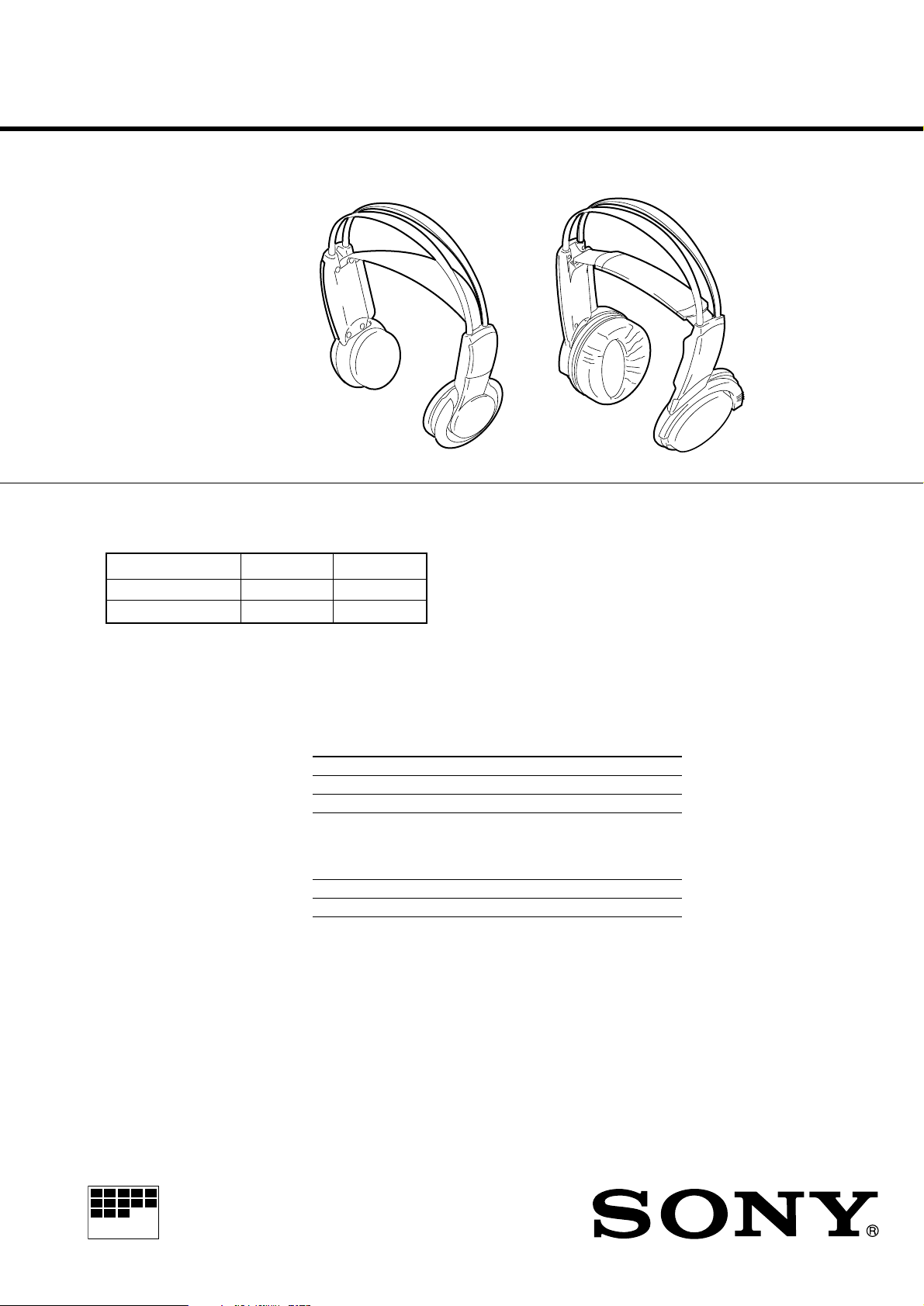
MDR-RF430/RF450
SERVICE MANUAL
Ver 1.1 2000.12
Illustration : MDR-RF430
MDR-RF430 is the component model block one in the MDR-RF430RK.
MDR-RF450 is the component model block one in the MDR-RF450RK.
COMPONENT MODEL NAME FOR MDR-RF430RK/RF450RK
MDR-RF430RK MDR-RF450RK
Wireless Headphones MDR-RF430 MDR-RF450
Transmitter TMR-RF450R TMR-RF450R
AEP Model
Illustration : MDR-RF450
SPECIFICATIONS
Headphone
Charging and using hours
Approx. charging hours Approx. using time*
1 50 minutes
24** 20 hours
* at 1kHz 1mW + 1mW output
** the hours required to fully charge empty batteries
Battery life
Battery Approx. hours*
Sony alkaline battery LR6 (SG) 60
Sony battery R6P (SR) 30
* at 1kHz 1mW + 1mW output
Power source DC 3V : 2 x R6 (size AA) battery or 2 x supplied
Mass Approx. 215g (7.6oz.) incl.Ni-Cd batteries (MDR-RF430RK)
Supplied Ni-Cd rechargeable batteries
Model name NC-AA-HJ
Voltage 1.2V
Capacity 600mAh
Design and specifications are subject to change without notice.
NC-AA-HJ Ni-Cd rechargeable battery
Approx. 265g (9.4oz.) incl.Ni-Cd batteries (MDR-RF450RK)
WIRELESS STEREO HEADPHONES
MICROFILM
Page 2
SECTION 1
d
)
DISASSEMBLY
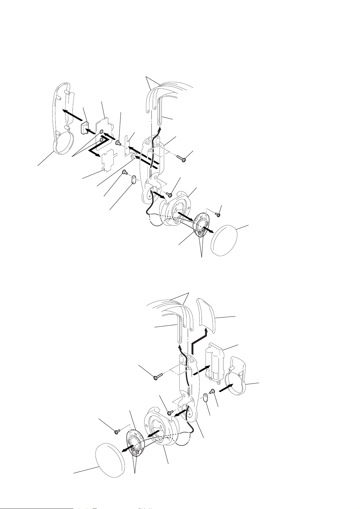
Note : Follow the disassembly procedure in the numerical order given.
MDR-RF430
1-1. RX BOARD, FE BOARD, RECEIVER (R-CH), SUSPENDER REMOVAL
Head band
5
RX board
FE board
4
8
9
Screw
(M1.7x4)
Spacer
!¶
Suspender
Hanger (R)
Hanger cover (R)
RX shield plate
7
Remove
solder
6
SW1
!™
Screw
+P 2x6
!º
!¡
!£
Ball shaft holder
MDD02 (R-CH)
2
3
Screws +P 2x5
Housing (R) assy
!∞
1-2. BATTERY CASE, RECEIVER (L-CH), SUSPENDER REMOVAL
Head band
Screws +P 2x10
!¢
Screw (M 1.7x4)
1
!§
Remove solder
Ear pa
Battery cover
9
Screw (M 1.7x4)
Ear pad
2
Screws +P 2x10
3
MDD01 (L-CH)
1
Suspender
Screws +P 2x5
!º
!¡
Remove solder
!™
8
Housing (L) assy
– 2 –
5
6
Ball shaft holder
Hanger (L)
4
7
Screw +P 2x6
Battery case
Hanger cover (L
Page 3
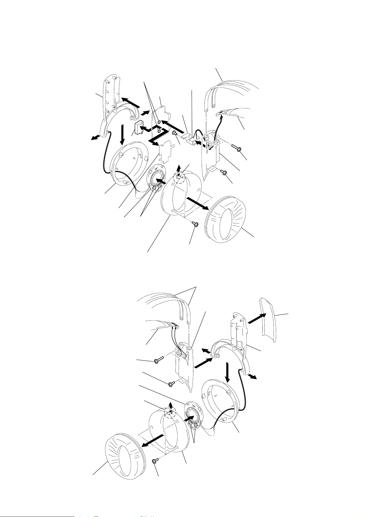
MDR-RF450
r
1-1. RECEIVER (R-CH), RX BOARD, FE BOARD, SUSPENDER ASSY REMOVAL
Head band
!£
Remove
Hanger (R)
solder
RX board
8
9
Surpport switch
!¶
SW
board
9
Housing (R)
RX shield plate
MDD02 (R-CH)
0
!¢
FE board
3
Remove
solder
Front plat (R) assy
5
!™
!¡
Screw
(M1.7x4)
4
Claw
2
Screws
(M 1.7x4)
1-2. RECEIVER (L-CH), SUSPENDER ASSY REMOVAL
Head band
!∞
1
!§
7
Screws (M1.7x4)
Suspender
6
Screws +P 2x8
Hanger cover (R)
Ear pad
Ear pad
Suspender
9
Screws +P 2x8
0
Screws (M 1.7x4)
MDD01 (L-CH)
Claw
4
1
2
Screws
(M 1.7x5) tapping
Hanger cover (L)
!™
6
!¡
5
3
Remove solder
Front plate (L) assy
8
Battery cove
7
Hanger (L)
6
Housing (L)
– 3 –
Page 4
SECTION 2
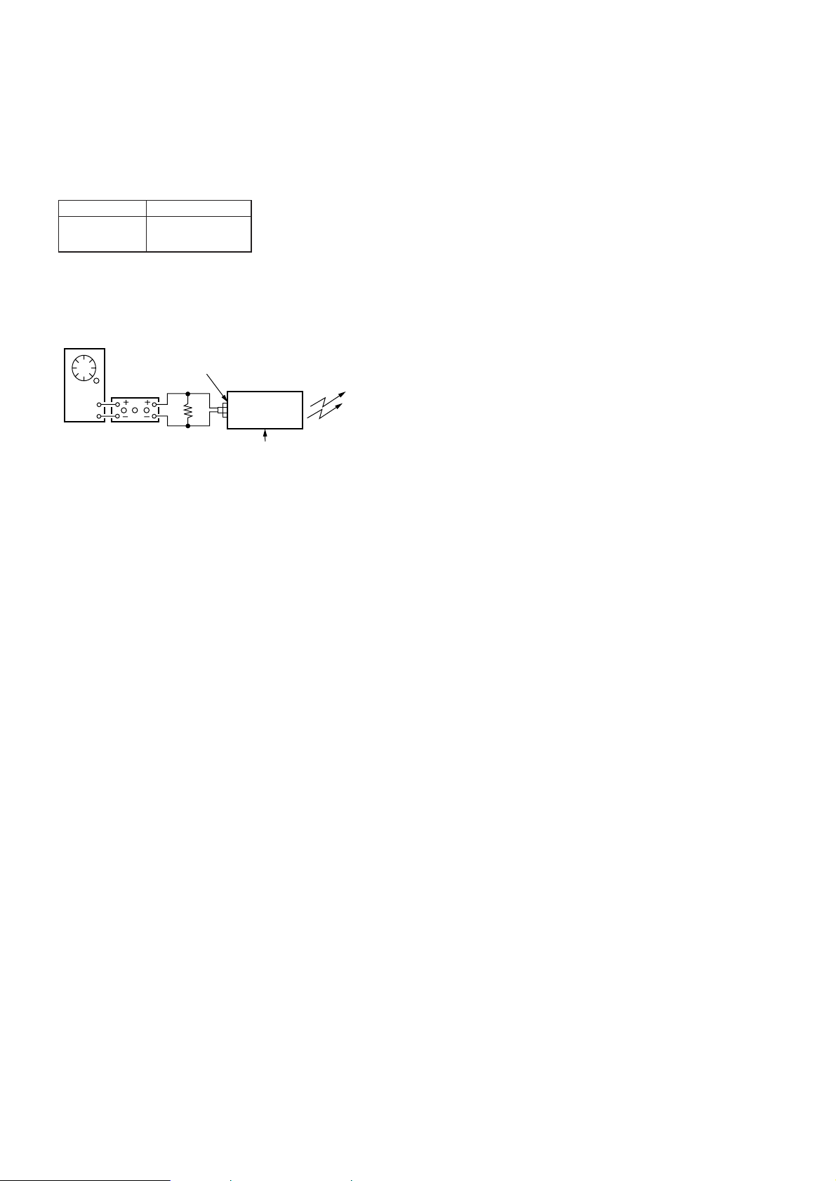
ELECTRICAL ADJUSTMENTS
Note :
1. Use transmitter with check and adjustment already completed.
2. The transmitter section adjustments should be completed before
performing the headphones section adjustment.
3. On adjusting the headphones section, use the transmitter as a
jig.
Headphones Transmitter
MDR-RF430
MDR-RF450
Setting :
AF OSC
1. Feed a signal to jig (transmitter) and connect a power supply to
DC IN 9V jack (J404).
TMR-RF450R
L-CH (J403)
1kHz 316mVrms (–7.8dB)
ATT
600
Ω
Jig
Transmitter
J404
power supply
(DC 11V)
Separation check and adjustment
1. Set the transmitter channel to CH2.
2. Set the transmitter noise filter SW to OFF .
3. Input a signal of 1kHz 316mVrms to onl y the transmitter L-c h
(J403).
4. Connect an digital voltmeter (AC range) and oscilloscope to
the L-ch speaker outputs (both sides of MDD01).
5. Receive signals b y turning the TUNING V OL (RV302).
6. Adjust the VOL (RV301) so that the RX boar d L-c h speaker
outputs (both sides of MDD01) are 155mVrms.
7. Connect an digital voltmeter (AC range) and oscilloscope to
the R-ch speaker outputs (both sides of MDD02) and measure
the voltages.
8. At this time, check to make sure the level separation of L-ch
and R-ch speaker outputs is more than 20dB. If the separation
is less than 20dB, turn R V303 on the RX boar d so that the R-c h
output is minimal, then check to see if the level separation of Lch and R-ch speaker outputs is more than 20dB.
9. Input a signal of 1kHz 316mVrms to onl y the transmitter R-c h
(J402).
10. Adjust the V OL (RV301) so that the RX boar d R-c h speaker
outputs (both sides of MDD02) are 155mVrms.
11. Connect an digital voltmeter (AC range) and oscilloscope to
the L-ch speaker outputs (both sides of MDD01) and measure
the voltages.
12. At this time, check to make sure the level separation of L-ch
and R-ch speaker outputs is more than 20dB.
Receive frequency check and adjustment
1. Set the transmitter channel to CH2.
2. Set the transmitter noise filter SW to OFF .
3. Input a signal of 1kHz 316mVrms to onl y the transmitter L-c h
(J403).
4. Place transmitter and headphones at a distance of more than 5m
apart.
5. Set the V OL (RV301) to MIN.
6. Position RX boar d TUNING V OL (RV302) to the center .
7. Connect a digital voltmeter (DC range) and an oscilloscope between IC301 pin @¡ and GND.
8. First check to make sure that a demodulated waveform of 1kHz
(appr oximatel y 13mVrms) is outputted to the oscilloscope , then
chec k to make sure the DC v oltmeter reading is DC 1–1.2V .
9. If a demodulated waveform of 1kHz is not outputted to the oscilloscope or if the DC level is not within the range specified
above, adjust the RX board L301 so that a demodulated waveform of 1kHz is outputted to the oscilloscope and while the waveform is outputted, further fine adjust the L301 so that the DC
voltmeter reading is DC 1.1V .
10. When completed, make sure signals can be received when switching the transmitter channel to CH1 or CH3 by turning RX board
TUNING V OL (RV302).
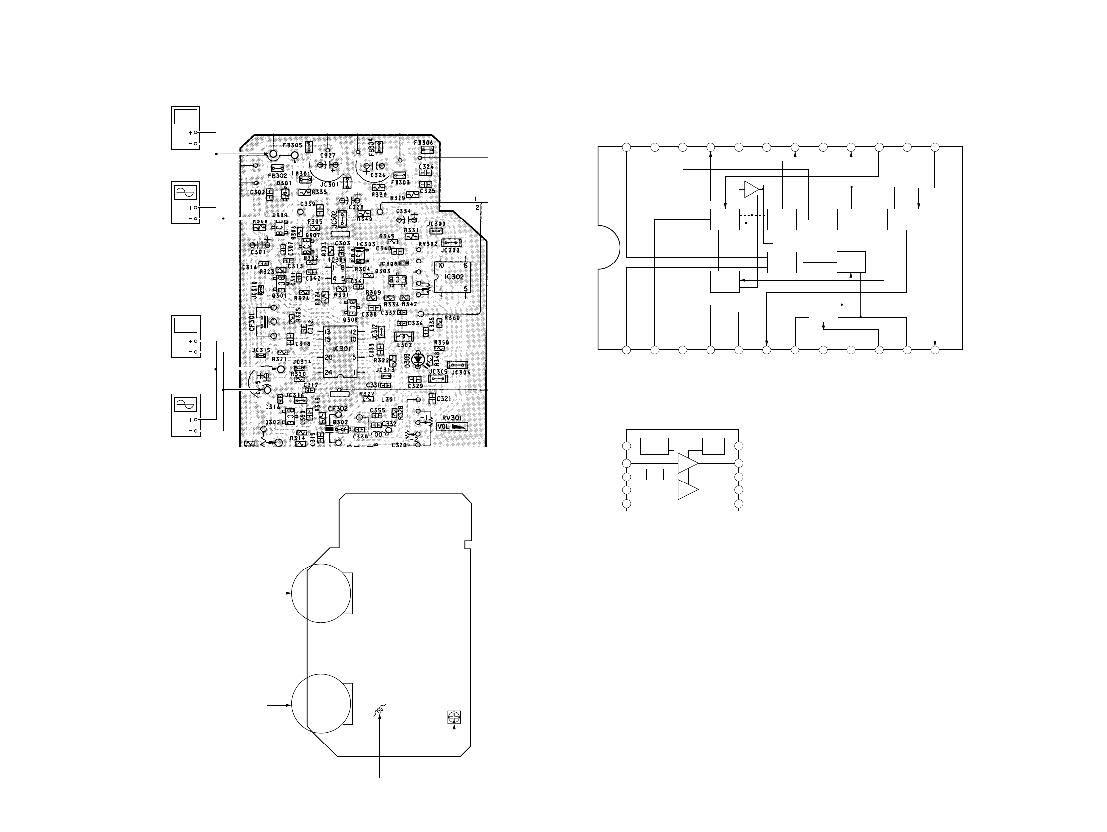
Connection points and Adjustment Location :
RX board (See page 5)
Connection points and Adjustment Location :
RX board (See page 5)
– 4 –
Page 5
t
POWER
SWITCH
MUTE
CIRCIUT
BIAS
1
2
3
4
5
6
7
8
9
10
MT/SW
OUT1
POWER GND
OUT2
VCC
P/SW
IN1
PRE GND
IN2
REF
AMP2
AMP1
SECTION 3
DIAGRAMS
Connection points :
digital voltmeter
(AC range)
oscilloscope
digital voltmeter
(DC range)
oscilloscope
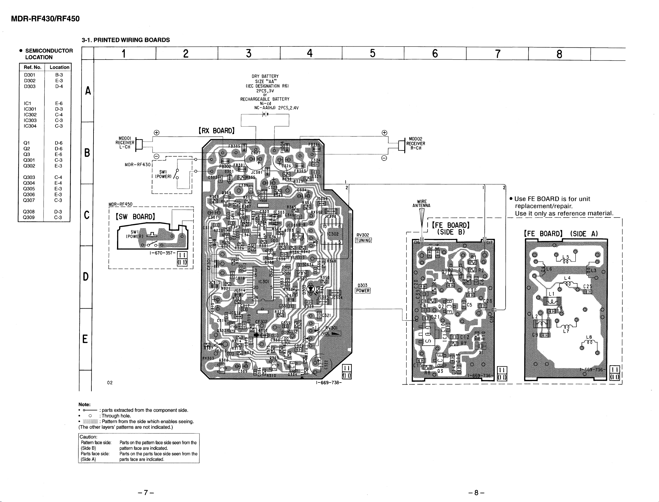
[ RX BOARD ] (Conductor side)
r
IC BLOCK DIAGRAMS
IC301 CXA1611N-T4
DETUNE DET
CONTROL
24 23 22 21 20 19 18 17 16 15 14 13
1 2 3 4 5 6 7 8 9 10 11 12
DETUNE DET
VCC
GND
FM DISCRI
RIPPLE FILTER
DET OUT
DET•AGC
AFC
AM OSC
FM•IF
DISCRI
AM•IF
AFC AGC
FM OSC
AFC AGC
TUNING
METER
DETUNE
DET
REG OUT
AM IF OUT
FM RF
FM•FE
GND
AM RF IN
RIPPLE
FILTER
AM•FE
METER
NC
FM IF IN
REGULATOR
FM RF IN
AM IF IN
GND
FM/AM
BAND SELECT
FM/AM
FE OUT
Adjustment Location :
IC302 LA4533M
[RX BOARD] (Component side)
RV302
Tuning Knob
RV301
VOL Knob
RV303 : Separation Adjustmen
L301 : Receive Frequency Adjustment
– 5 – – 6 –
Page 6
Page 7
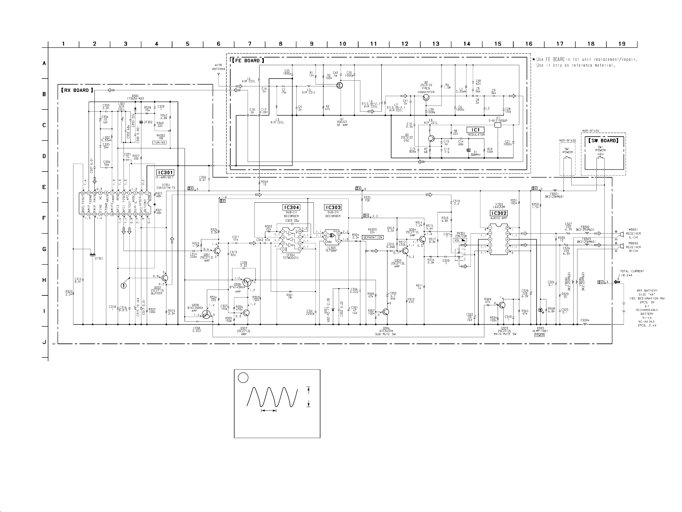
3-2. SCHEMATIC DIAGRAM
r
Refer to page 6 for IC Block Diagrams.
MDR-RF430/RF450
Note:
• All capacitors are in µF unless otherwise noted. pF: µµF
50 WV or less are not indicated except for electrolytics
and tantalums.
• All resistors are in Ω and 1/
specified.
¢
•
• U : B+ Line.
• H : adjustment for repair.
• Power voltage is dc 3V and fed with regulated dc power
• Voltages are dc with respect to ground under no-signal
• Voltages are taken with a V OM (Input impedance 10 MΩ).
• Waveforms are taken with a oscilloscope.
• Circled numbers refer to waveforms.
• Signal path.
: internal component.
supply from battery terminal.
conditions.
Voltage variations may be noted due to normal produc-
tion tolerances.
Voltage variations may be noted due to normal produc-
tion tolerances.
F
4
W or less unless otherwise
r
WA VEFORM
1
10mVp-p
µ
sec
20.4
IC301 @¡
– 9 – – 10 –
VOL T/DIV : 2m V AC
TIME/DIV : 20 µsec
Page 8
NOTE :
• -XX, -X mean standardized parts, so they
may have some difference from the original
one.
• Items marked “ * ”are not stocked since they
are seldom required for routine service. Some
delay should be anticipated when ordering
these items.
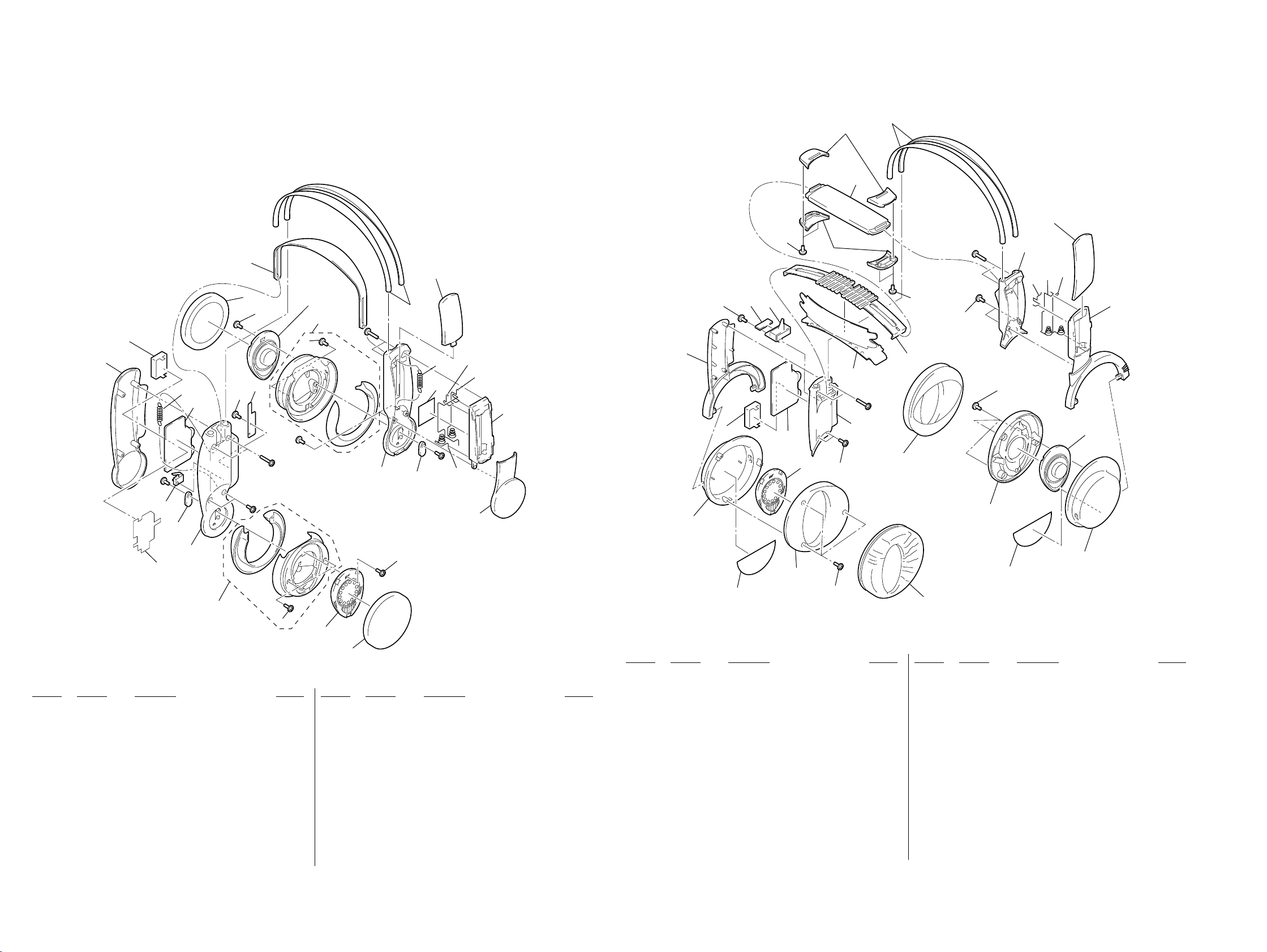
4-1. MDR-RF430
SECTION 4
EXPLODED VIEWS
• The mechanical parts with no reference
number in the exploded views are not
supplied.
• Hardware (# mark) list and accessories and
packing materials are given in the last of this
parts list.
Ver 1.1 2000.12
4-2. MDR-RF450
65
63
64
69
10
12
1
8
24
7
MDD01
13
8
#3
11
14
15
16
22
17
#2
4
18
19
#2
SW1
14
9
8
6
#1
#3
#1
20
4
3
5
8
2
8
MDD02
1
Ref. No. Part No. Description Remark Ref. No. Part No. Description Remark
1 4-994-129-01 PAD, EAR
2 X-4950-086-1 HOUSING (R) ASSY
3 4-994-119-01 HANGER (R)
4 4-992-281-01 HOLDER, BALL SHAFT
5 4-210-280-01 PLATE, RX SHIELD
* 6 A-4542-510-A RX BOARD, COMPLETE
7 4-994-121-01 COVER (R), HANGER
8 3-713-791-01 SCREW (M1.7X4), TAPPING, P2
9 4-995-597-01 SPACER
10 4-994-124-01 SUSPENDER
11 4-994-118-01 BAND, HEAD
12 4-994-123-01 COVER, BATTERY
13 X-4950-087-1 HOUSING (L) ASSY
14 4-995-475-01 SPRING, TENSION
15 4-994-130-01 TERMINAL (+), BATTERY
16 4-994-132-01 TERMINAL (MIDWAY), BATTERY
17 4-993-020-01 CASE, BATTERY
18 4-994-131-01 TERMINAL (-), BATTERY
19 4-994-122-01 COVER (L), HANGER
20 4-994-120-01 HANGER (L)
22 3-831-441-99 CUSHION, SPEAKER
* 24 A-4542-531-A FE BOARD, COMPLETE
MDD01 1-505-117-21 RECEIVER (L-CH)
MDD02 1-505-117-21 RECEIVER (R-CH)
SW1 1-771-249-11 SWITCH, PUSH (1 KEY) (POWER)
57
59
58
61
62
#4
61
73
71
70
72
68
57
56
66
67
57
#4
77
55
MDD02
57
60
51
MDD01
75
54
74
52
53
Ref. No. Part No. Description Remark Ref. No. Part No. Description Remark
51 4-977-785-01 PAD, EAR
52 X-4950-101-1 PLATE (R) ASSY, FRONT
53 4-999-774-01 REGISTER, HOUSING
54 4-999-773-01 HOUSING (R)
* 55 A-4542-510-A RX BOARD, COMPLETE
56 4-999-769-01 COVER (R), HANGER
57 3-713-791-01 SCREW (M1.7X4), TAPPING, P2
58 4-210-255-01 SUPPORT, SWITCH
* 59 1-670-357-11 SW BOARD
60 4-999-767-01 HANGER (R)
61 3-318-203-62 SCREW (B1.7X4), TAPPING
* 62 4-999-791-01 PANEL, BACK
* 63 4-999-792-01 CASE
64 4-978-519-01 CUSHION, HEAD
65 4-999-765-01 BAND, HEAD
57
51
66 4-999-771-01 SUSPENDER
67 4-978-518-02 BASE, SUSPENDER
68 4-999-768-01 COVER (L), HANGER
69 4-999-770-01 BATTERY COVER
70 4-210-258-01 TERMINAL (MIDWAY), BATTERY
71 4-210-256-01 TERMINAL (+), BATTERY
72 4-210-257-01 TERMINAL (-), BATTERY
73 4-999-766-01 HANGER (L)
74 4-999-772-01 HOUSING (L)
75 X-4950-100-1 PLATE (L) ASSY, FRONT
* 77 A-4542-531-A FE BOARD, COMPLETE
MDD01 1-505-117-21 RECEIVER (L-CH)
MDD02 1-505-117-21 RECEIVER (R-CH)
53
– 11 – – 12 –
Page 9
SECTION 5
ELECTRICAL PARTS LIST
NOTE :
• Due to standardization, replacements in the
parts list may be different from the parts
specified in the diagrams or the components
used on the set.
• -XX, -X mean standardized parts, so they
may have some difference from the original
one.
• RESISTORS
All resistors are in ohms
METAL : Metal-film resistor
METAL OXIDE :Metal oxide-film resistor
F : nonflammable
• Items marked “ * ”are not stocked since
they are seldom required for routine service.
Some delay should be anticipated when
ordering these items.
Ref. No. Part No. Description Remark Ref. No. Part No. Description Remark
* A-4542-531-A FE BOARD, COMPLETE
******************
*************************************************************
* A-4542-510-A RX BOARD, COMPLETE
******************
• SEMICONDUCTORS
In each case, u : µ , for example :
uA.... : µ A.... , uPA.... : µ PA....
uPB.... : µ PB.... , uPC.... : µPC....
uPD.... : µ PD....
• CAPACITORS
uF : µ F
• COILS
uH : µ H
C340 1-164-346-11 CERAMIC CHIP 1uF 16V
C341 1-162-966-11 CERAMIC CHIP 0.0022uF 10% 50V
C342 1-162-923-11 CERAMIC CHIP 47PF 5% 50V
C350 1-163-021-91 CERAMIC CHIP 0.01uF 10% 50V
C355 1-162-919-91 CERAMIC CHIP 22PF 0.5PF 50V
When indicating parts by reference number, please include the board.
< FILTER >
RXFE
< CAPACITOR >
C301 1-124-589-11 ELECT 47uF 20% 16V
C302 1-164-489-11 CERAMIC CHIP 0.22uF 10% 16V
C303 1-162-921-11 CERAMIC CHIP 33PF 5% 50V
C306 1-164-227-11 CERAMIC CHIP 0.022uF 10% 25V
C307 1-162-927-11 CERAMIC CHIP 100PF 5% 50V
C309 1-126-572-11 ELECT 4.7uF 20% 35V
C310 1-110-563-11 CERAMIC CHIP 0.068uF 10% 16V
C311 1-162-923-11 CERAMIC CHIP 47PF 5% 50V
C312 1-162-970-11 CERAMIC CHIP 0.01uF 10% 25V
C313 1-162-926-11 CERAMIC CHIP 82PF 5% 50V
C314 1-162-957-11 CERAMIC CHIP 220PF 5% 50V
C315 1-124-233-11 ELECT 10uF 20% 16V
C316 1-164-245-11 CERAMIC CHIP 0.015uF 10% 25V
C317 1-162-970-11 CERAMIC CHIP 0.01uF 10% 25V
C318 1-164-346-11 CERAMIC CHIP 1uF 16V
C319 1-164-505-11 CERAMIC CHIP 2.2uF 16V
C320 1-164-346-11 CERAMIC CHIP 1uF 16V
C321 1-164-346-11 CERAMIC CHIP 1uF 16V
C322 1-124-242-00 ELECT 33uF 20% 25V
C324 1-107-725-11 CERAMIC CHIP 0.1uF 10% 16V
C325 1-107-725-11 CERAMIC CHIP 0.1uF 10% 16V
C326 1-124-635-00 ELECT 220uF 20% 6.3V
C327 1-124-635-00 ELECT 220uF 20% 6.3V
C328 1-124-635-00 ELECT 220uF 20% 6.3V
C329 1-164-346-11 CERAMIC CHIP 1uF 16V
C330 1-162-964-11 CERAMIC CHIP 0.001uF 10% 50V
C331 1-162-912-11 CERAMIC CHIP 7PF 0.5PF 50V
C332 1-164-441-91 CERAMIC CHIP 68PF 5% 50V
C333 1-163-021-91 CERAMIC CHIP 0.01uF 10% 50V
C334 1-124-233-11 ELECT 10uF 20% 16V
C335 1-162-924-11 CERAMIC CHIP 56PF 5% 50V
C336 1-162-924-11 CERAMIC CHIP 56PF 5% 50V
C337 1-162-970-11 CERAMIC CHIP 0.01uF 10% 25V
C338 1-163-037-11 CERAMIC CHIP 0.022uF 10% 25V
C339 1-164-489-11 CERAMIC CHIP 0.22uF 10% 16V
CF301 1-577-588-11 FILTER, CERAMIC
CF302 1-567-163-11 FILTER, CERAMIC
< DIODE >
D301 8-719-045-99 DIODE RD2.2M-T1B
D302 8-719-002-81 DIODE 1T363
D303 8-719-023-84 LED HLMP-1801 (POWER)
< FERRITE BEAD >
FB301 1-414-234-11 INDUCTOR CHIP
FB302 1-414-234-11 INDUCTOR CHIP
FB303 1-414-234-11 INDUCTOR CHIP
FB304 1-414-234-11 INDUCTOR CHIP
FB305 1-414-234-11 INDUCTOR CHIP
FB306 1-414-234-11 INDUCTOR CHIP
< IC >
IC301 8-752-066-93 IC CXA1611N-T4
IC302 8-759-802-75 IC LA4533M
IC303 8-759-195-02 IC TC7S86F-TE85L
IC304 8-759-096-87 IC TC7WU04FU(TE12R)
< JUMPER RESISTOR >
JC301 1-216-295-00 METAL CHIP 0 5% 1/10W
JC302 1-216-296-00 METAL CHIP 0 5% 1/8W
JC303 1-216-296-00 METAL CHIP 0 5% 1/8W
JC304 1-216-296-00 METAL CHIP 0 5% 1/8W
JC305 1-216-296-00 METAL CHIP 0 5% 1/8W
JC308 1-216-864-11 METAL CHIP 0 5% 1/16W
JC309 1-216-295-00 METAL CHIP 0 5% 1/10W
JC310 1-216-864-11 METAL CHIP 0 5% 1/16W
JC312 1-216-295-00 METAL CHIP 0 5% 1/10W
JC313 1-216-864-11 METAL CHIP 0 5% 1/16W
JC314 1-216-864-11 METAL CHIP 0 5% 1/16W
JC315 1-216-864-11 METAL CHIP 0 5% 1/16W
JC316 1-216-295-00 METAL CHIP 0 5% 1/10W
– 13 –
Page 10

MDR-RF430/RF450
RX SW
Ref. No. Part No. Description Remark Ref. No. Part No. Description Remark
< COIL >
< VARIABLE RESISTOR >
L301 1-422-317-31 COIL, AIR-CORE
L302 1-412-933-11 INDUCTOR 0.33uH
< TRANSISTOR >
Q301 8-729-230-49 TRANSISTOR 2SC2712-YG
Q302 8-729-230-49 TRANSISTOR 2SC2712-YG
Q303 8-729-230-49 TRANSISTOR 2SC2712-YG
Q304 8-729-230-49 TRANSISTOR 2SC2712-YG
Q305 8-729-230-49 TRANSISTOR 2SC2712-YG
Q306 8-729-920-31 TRANSISTOR DTC343TK
Q307 8-729-230-49 TRANSISTOR 2SC2712-YG
Q308 8-729-040-78 TRANSISTOR DTA124GKA-T146
Q309 8-729-027-36 TRANSISTOR DTA143XKA-T146
< RESISTOR >
R301 1-216-857-11 METAL CHIP 1M 5% 1/16W
R302 1-216-847-91 METAL CHIP 150K 5% 1/10W
R303 1-216-837-91 METAL CHIP 22K 5% 1/10W
R304 1-216-827-11 METAL CHIP 3.3K 5% 1/16W
R305 1-216-847-91 METAL CHIP 150K 5% 1/10W
R306 1-216-853-11 METAL CHIP 470K 5% 1/16W
R307 1-216-845-11 METAL CHIP 100K 5% 1/16W
R308 1-216-089-91 RES,CHIP 47K 5% 1/10W
R309 1-216-841-11 METAL CHIP 47K 5% 1/16W
R310 1-216-817-11 METAL CHIP 470 5% 1/16W
R311 1-216-821-11 METAL CHIP 1K 5% 1/16W
R312 1-216-853-11 METAL CHIP 470K 5% 1/16W
R313 1-216-827-11 METAL CHIP 3.3K 5% 1/16W
R314 1-216-822-11 METAL CHIP 1.2K 5% 1/16W
R315 1-216-830-11 METAL CHIP 5.6K 5% 1/16W
RV301 1-223-968-11 RES, VAR, CARBON 20K/20K (VOL)
RV302 1-225-641-11 RES, VAR, CARBON 10K (TUNING)
RV303 1-238-601-11 RES, ADJ, CARBON 22K (SEPARATION)
************************************************************
* 1-670-357-11 SW BOARD (RF450)
**********
< SWITCH >
SW1 1-572-467-61 SWITCH, PUSH (1 KEY) (POWER) (RF450)
************************************************************
MISCELLANEOUS
**************
MDD01 1-505-117-21 RECEIVER (L-CH) (RF430)
MDD01 1-505-117-21 RECEIVER (L-CH) (RF450)
MDD02 1-505-117-21 RECEIVER (R-CH) (RF430)
MDD02 1-505-117-21 RECEIVER (R-CH) (RF450)
SW1 1-771-249-11 SWITCH, PUSH (1 KEY) (POWER) (RF430)
************************************************************
**************
HARDWARE LIST
**************
#1 7-685-103-19 SCREW +P 2X5 TYPE2 NON-SLIT (RF430)
#2 7-685-104-19 SCREW +P 2X6 TYPE2 NON-SLIT (RF430)
#3 7-685-106-19 SCREW +P 2X10 TYPE2 NON-SLIT (RF430)
#4 7-685-105-19 SCREW +P 2X8 TYPE2 NON-SLIT (RF450)
R316 1-216-827-11 METAL CHIP 3.3K 5% 1/16W
R317 1-216-827-11 METAL CHIP 3.3K 5% 1/16W
R318 1-216-831-91 RES,CHIP 6.8K 1% 1/10W
R319 1-216-061-00 METAL CHIP 3.3K 5% 1/10W
R320 1-216-845-11 METAL CHIP 100K 5% 1/16W
R321 1-216-843-11 METAL CHIP 68K 5% 1/16W
R322 1-216-843-11 METAL CHIP 68K 5% 1/16W
R323 1-216-859-11 RES,CHIP 1.5M 5% 1/16W
R324 1-216-033-00 METAL CHIP 220 5% 1/10W
R325 1-216-825-91 METAL CHIP 2.2K 5% 1/16W
R326 1-216-827-11 METAL CHIP 3.3K 5% 1/16W
R327 1-216-809-11 METAL CHIP 100 5% 1/16W
R328 1-216-835-11 METAL CHIP 15K 5% 1/16W
R329 1-216-001-00 METAL CHIP 10 5% 1/10W
R330 1-216-001-00 METAL CHIP 10 5% 1/10W
R331 1-216-097-91 RES,CHIP 100K 5% 1/10W
R334 1-216-845-11 METAL CHIP 100K 5% 1/16W
R335 1-216-029-00 METAL CHIP 150 5% 1/10W
R342 1-216-831-11 METAL CHIP 6.8K 5% 1/16W
R345 1-216-841-11 METAL CHIP 47K 5% 1/16W
R348 1-216-831-11 METAL CHIP 6.8K 5% 1/16W
R349 1-216-001-00 METAL CHIP 10 5% 1/10W
R350 1-216-823-11 METAL CHIP 1.5K 5% 1/16W
R360 1-216-837-91 METAL CHIP 22K 5% 1/10W
9-924-917-11
Sony Corporation
Personal A&V Products Company
– 14 –
Printed in Hungary © 1998.6
98F027539-1
Published by Quality Engineering Dept.
(Shibaura)
 Loading...