

Page 1
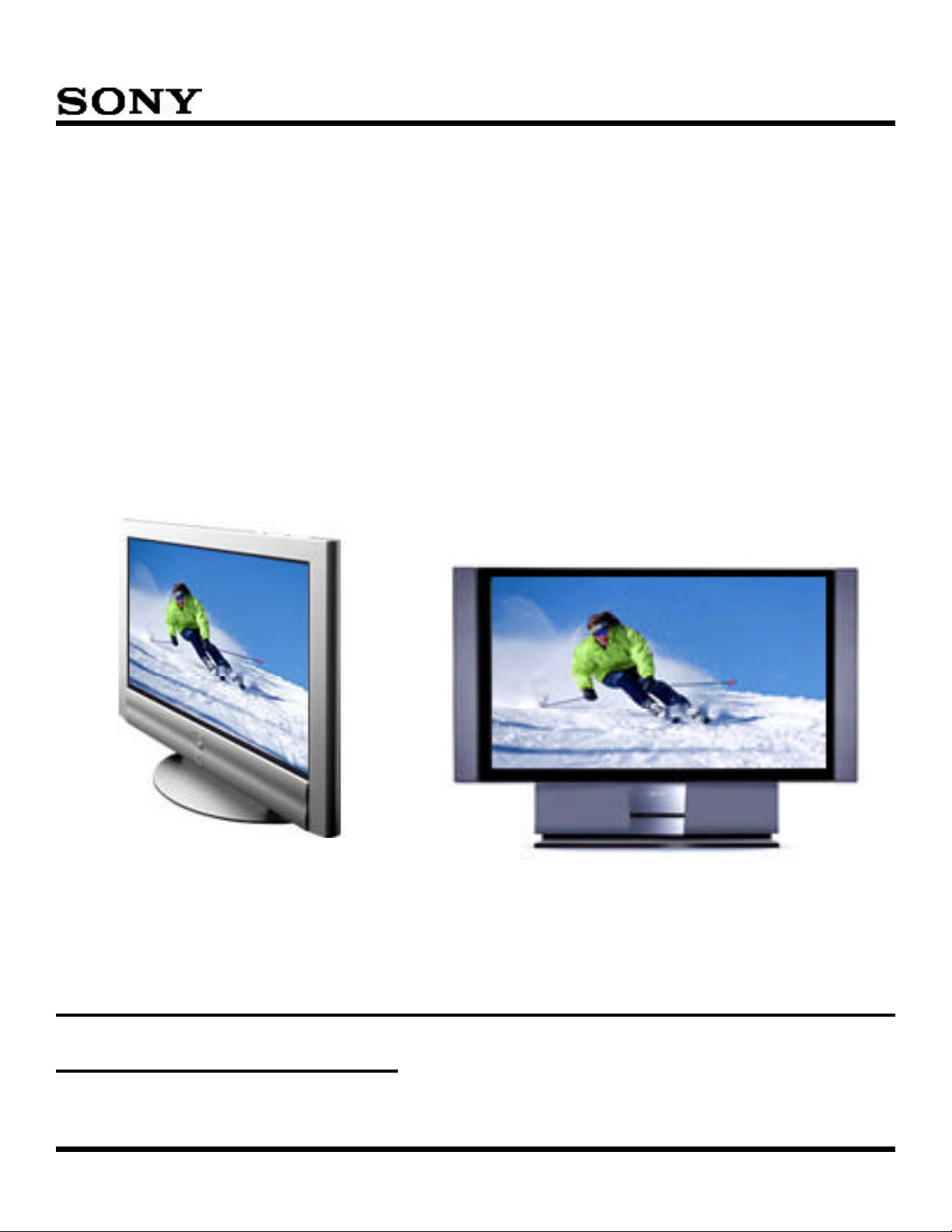
Training Manual
Plasma TV &
Grand Wega Projection TV
Models: KZ-32TS1U
KZ-41TS1U
KF-60DX100
KZ-32TS1U
Diagnostic Guides
Course: TVP-13
KF-60DX100
Page 2

Table of Contents
KZ-32TS1U // KZ-42TS1U
Introduction ...........................................1
1. Normal Operation .............................2
2. Self-Diagnostics................................3
3. Board Selection by Defect...............4
4. Plasma Panel Picture Defects .........5
5. Board Location..................................6
6. Service Mode.....................................7
7. Adjustments when the
B Board is Replaced............................12
8. Plasma Panel Replacement -
KZ-32TS1U ............................................15
9. Plasma Panel Replacement -
KZ-42TS1U ............................................23
10. Standby Power / Power ON..........28
Power ON .............................................................. 28
11. Fan Drive Circuit ............................30
12. Video Signal Flow ..........................32
13. What is Flat Screen
Plasma Technology? ...........................35
Theory of Operation ............................................ 35
KF-60DX100
Introduction ..........................................37
15. Normal Operation ..........................38
16. Self-Diagnostics.............................39
17. Board Selection by Defect............40
18. Board Locations.............................41
19. Adjustments ....................................42
20. Service Mode..................................44
21. Determining if the
Optical Unit is OK ................................45
22. Optical Unit Removal ....................46
23. Screen / Mirror Replacement.......50
24. Troubleshooting -
TV Shutdown ........................................53
25. Power Supply .................................54
26. Fan Control - KF-60DX100............56
27. Grand Wega Lamp Control...........59
Lamp Operation ................................................... 59
Lamp ON Display ................................................. 62
Power Block Location & Removal..................... 62
Troubleshooting.................................................... 63
28. Video Process ................................65
Page 3
Sony Model KZ-32TS1U // KZ-41TS1U TV Diagnostic Guide
Sony Plasma TV KZ-32TS1U/KZ-41TS1U Introduction
This training manual has been organized to provide a quick diagnosis of problems in Sony Plasma screen TV
models KZ-32TS1U and KZ-41TS1U. The circuitry in these two TV sets is similar, but the boards and plasma
panels are mounted differently.
Because the Plasma TV set is a new design concept, Chapter 1 will cover normal Plasma TV operation. The last
chapter will cover plasma principles / concepts (only necessary for background information).
Repairs to these TV models involve identifying and replacing a circuit board, the plasma panel or other parts
such as the fan or the on/off switch. This manual is divided into thirteen chapters:
Table of Contents
Chapter Contents
1. Normal Operation This 16x9 plasma screen TV operates differently from a picture
tube TV.
2. Self Diagnostics The front panel Standby light blinks to indicate major and minor
problems.
3. Board Selection by Defect Listing of possible defects and where they may be.
4. Plasma Panel picture
Defects
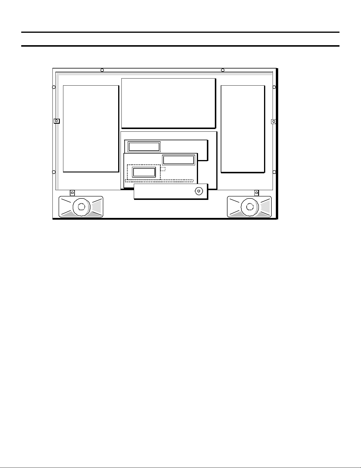
5. Board Location Location of replaceable boards in model KZ-32TS1U.
6. Service Mode Service Mode access and contents.
7. Adjustments Adjustments after the B board is replaced.
8. Plasma Panel
Replacement KZ32TS1U
9. Plasma Panel
Replacement KZ42TS1U
10. Standby power / Power
ON circuit description
11. Fan Drive circuit
description
12. Video Flow circuit
description
13. Plasma Display
Technology
Listing of possible plasma panel screen defects
Pictured procedure to avoid problems in access and reassembly.
KZ32TS1U and KZ42TS1U have separate pictured procedures.
Pictured procedure to avoid problems in access and reassembly.
KZ32TS1U and KZ42TS1U have separate pictured procedures.
Location and circuit operation for Standby voltage and Power ON
sequence.
Fan Operation, troubleshooting, and testing.
Signal levels, description and symptoms when missing.
Plasma Cell Operating Concepts
1
Page 4
Sony Model KZ-32TS1U // KZ-41TS1U TV Diagnostic Guide
Chapter 1 - Normal Operation
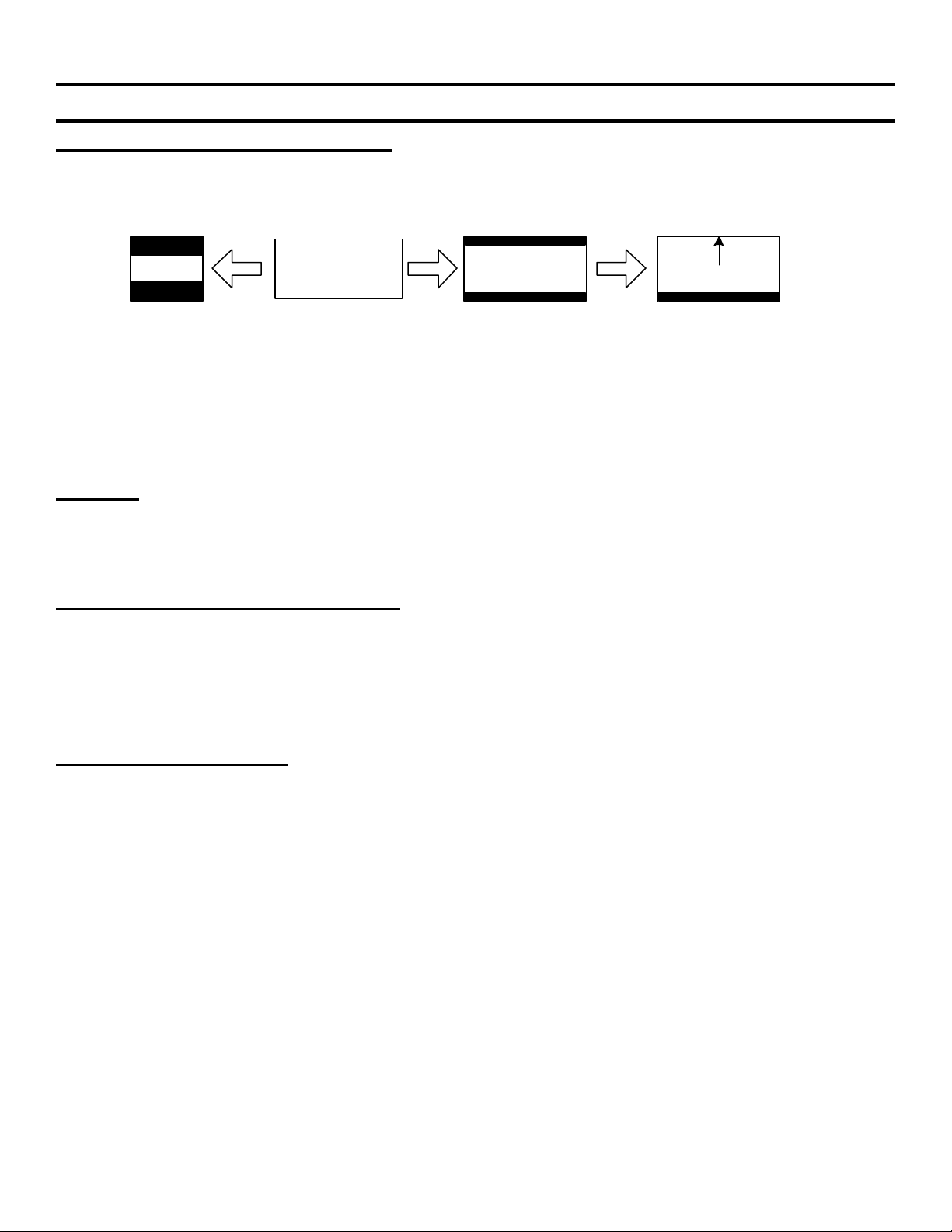
Black top and bottom (letterbox) borders – Even though this TV has a wide 16x9 screen, it is still possible to
receive a picture with top and bottom black bands. Movies are shot in many aspect ratios. The most common
ratios are 4:3, 1.85:1 and 2.35:1. The picture displayed is dependent upon what aspect ratio the movie was shot
in and how different it is from your TV screen’s aspect ratio. Ref Figure 1-1 below:
2:35:1 Movie
4x3 TV
Figure 1-1 - Display of a 2:35:1 Aspect Ratio Movie
The 1.85:1 aspect ratio movie will display without the black bands on this 16x9 screen TV (16/9 = 1.77:1 aspect
ratio) because their 1.85 and 1.77 aspect ratios are almost the same. The extra wide 2.35:1 aspect ratio movie
camera is still used in the film industry (mostly overseas). It produces the black borders even on a 16x9 (1.77:1)
TV screen. In this TV, you may choose the “Subtitle” screen mode from the menu to fill the top of the screen,
leaving only a black band at the bottom for the subtitle.
Fan Noise – Once the TV is turned on, the fan starts. The fan itself makes no noise but air flowing through the
TV does, especially when the TV is enclosed. This low level of air turbulence is normal. The Main CPU monitors
the fan run voltage, rotation and ambient temperature of the power supply. This information is available to the
user from the User Status menu as an OSD (on screen display OK or NG indication). Details such as the
temperature are in the Service Mode (see Section 6).
Video Inversion to prevent border burn in – After a (undetermined) period of use, some plasma cells will not
be as bright as others, causing an incorrect tint (because one of the red, green or blue plasma cells will darken,
leaving the others bright). Burn in can be prevented from the user menu. From the Screen Saver menu,
“Picture Inversion” may be selected to “clean” the screen (black becomes white and white becomes black
momentarily), restoring normal brightness to the cells.
If this Inversion function were set for AUTOmatic, picture inversion would occur at a specified time every day if
the TV were ON. This picture inversion may alarm a viewer that is not aware that this is normal for this TV.
Picture Shift / Picture Orbit – To reduce the possibility of a stationary image permanently “burnt” into the
plasma screen phosphor, the picture can be set to automatically move in a circular “orbit” pattern. The menu’s
“picture orbit” can be set to small, medium or large orbit range and its cycle time can be 10, 30, 60 seconds or 5
minutes. Picture Orbit must be turned ON (normally OFF) if the user usually watches constant pattern images
such as movies with borders, stock market scenes, etc.
16x9 TV
Subtitle Mode
2
Page 5
Sony Model KZ-32TS1U // KZ-41TS1U TV Diagnostic Guide
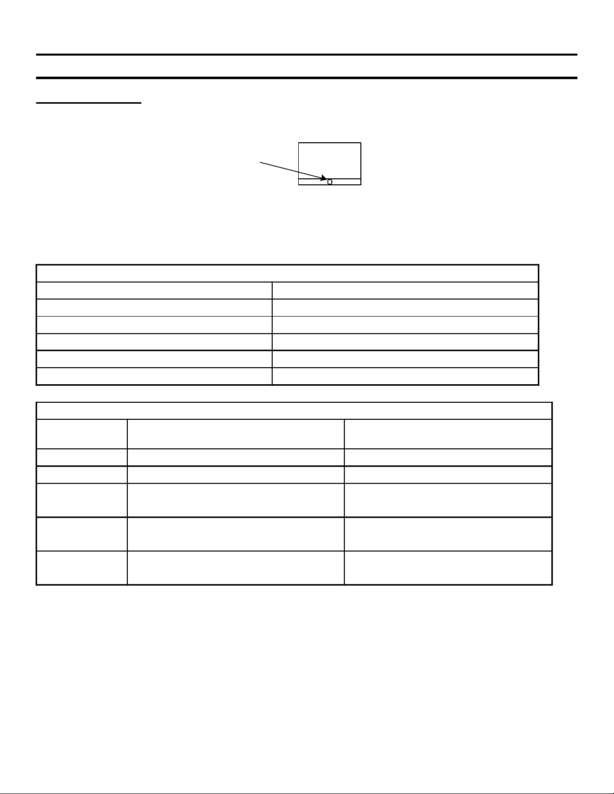
Figure 2-1
Chapter 2 - Self-Diagnostics
Standby/Sleep Light
The front panel Standby LED blinks to indicate a fault. Refer to Figure 2-1. If the TV does not start up, the
LED continually blinks to indicate a problem.
Standby/sleep
light
TV
If the TV starts and shuts down, the LED will repeatedly blink to indicate the reason for shutdown or A/V muting.
Table 2-1 shows the boards that can cause the Standby LED to blink continuously and Table 2-2 shows the
boards that cause shutdown.
Table 2–1 - Causes of Continuously Blinking LED – No TV A/V (black screen)
Cause Suspect Board
EEPROM ID check error B board
EEPROM read /write error B board
Color Decoder IC error B board
Panel will not initialize (start) Plasma panel
Low B+ at start up Plasma panel, power supply board
Table 2-2 - Cause of Standby LED Blinking in a Pattern - TV Shutdown
Times Standby
LED blinks
2 times Plasma panel error Plasma panel
Cause Suspected board
3 times Internal TV temperature at critical Q board, Fan, or possibly B board
4 times Digital 5Vdc output voltage excessive or
too low.
5 times Digital 3.3Vdc output voltage excessive or
too low.
6 times Analog 6Vdc output voltage excessive or
too low.
Power Supply Output CN1/pin 9 / 10
B board is the load - CN101.
Power Supply Output CN1/pin 5 / 6
B board is the load - CN101.
Power Supply Output CN1/pin 13 / 14
B board is the load - CN101.
3
Page 6
3. Board Selection by Defect
Chapter 3 - Board Selection by Defect
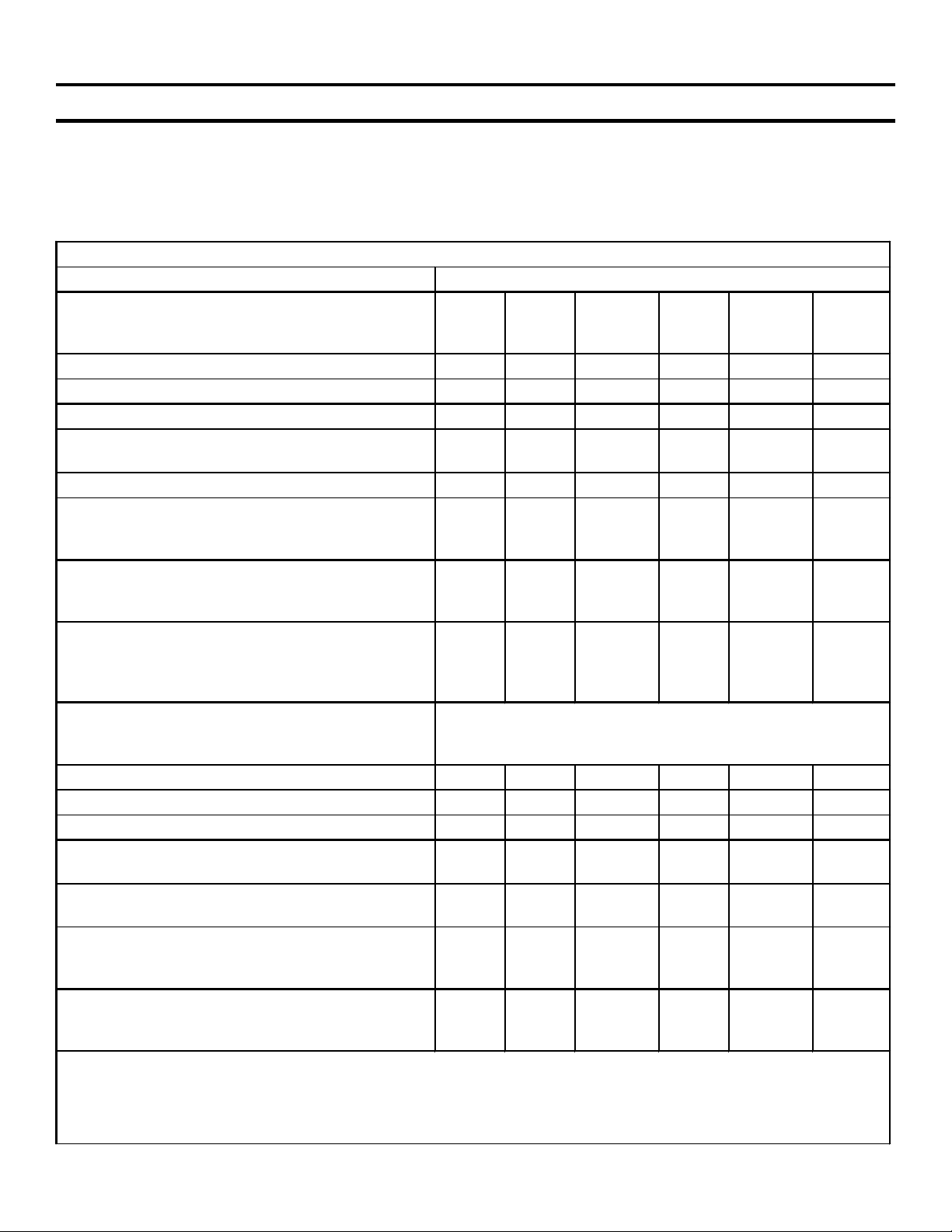
Table 3-1 shows the boards that could cause the symptoms listed. The most likely board is designated #1,
second likely #2, etc. Two #1 means both boards have an equal probability. To resolve the conflict, testing is
performed in the Standby/Power ON, Fan Drive, Video Flow circuit descriptions (Chapters 10-12) or the Plasma
Panel picture defects (Chapter 4).
For isolation purposes, the TU (tuner board) may be unplugged and the TV will work, displaying video inputs.
Table 3-1 - Plasma TV model KZ-32TS1U / KZ42TS1U Board Selection by Defect
Probable Circuit Board Failure
Symptom B* H1 Power
Supply**
Audio Problem – all inputs 2 1
Audio Problem – TV channels (deselect SAP)
Dark Screen – sound OK 1 2 1
Dark Picture – sound OK (deselect Power Save
on the remote)
Dead Set - No relay click at plug in 2 1 3
Dead Set – Stby light OFF. No response to
front panel pwr button. Plug-in relay click
heard.
Dead Set – Except for Stby light ON. No
response to pwr button. Plug-in relay click
heard.
Fan not cooling (front panel Standby indicator
blinking.) See the TV menu and Fan block
diagram in Section 7. Fan NG = No voltage to
fan. Temp NG = Fan not working.
Noise Bars across the screen (horizontal) The rear metal shield must contact the conductive mesh
Standby Indicator blinking 2 times
Standby Indicator blinking 3 times
Standby Indicator blinking 4, 5 or 6 times
Video Distortion – With composite and S video
input only.
Video Distortion – With component (Y, R-Y, B-
Y) input only.
Video Distortion – With both composite and
component inputs. Try using the menu’s
“picture inversion” to “clean” the screen first.
Symptom B * H1 Power
*After B board replacement, adjustments for brightness and color balance are necessary. See Adjustments.
**The entire power supply board is listed in the service manual as “Switching Regulator”. The 32” and 42”
TV sets do not use the same Switching Regulator power supply and therefore have different part numbers.
***See Possible Plasma Panel defects for illustrations.
2 1
1 1
3 2 1 4
2 1 3
3 2 1
on all four sides and be screwed to the center TV board
assembly.
2 1
3 (2 = fan)
2 1
2 1
2 1
1 2 3
Supply
Q TU Plasma
Panel
***
1
Q TU Plasma
Panel
**
4
Page 7
Chapter 4 - Plasma Panel Picture Defects
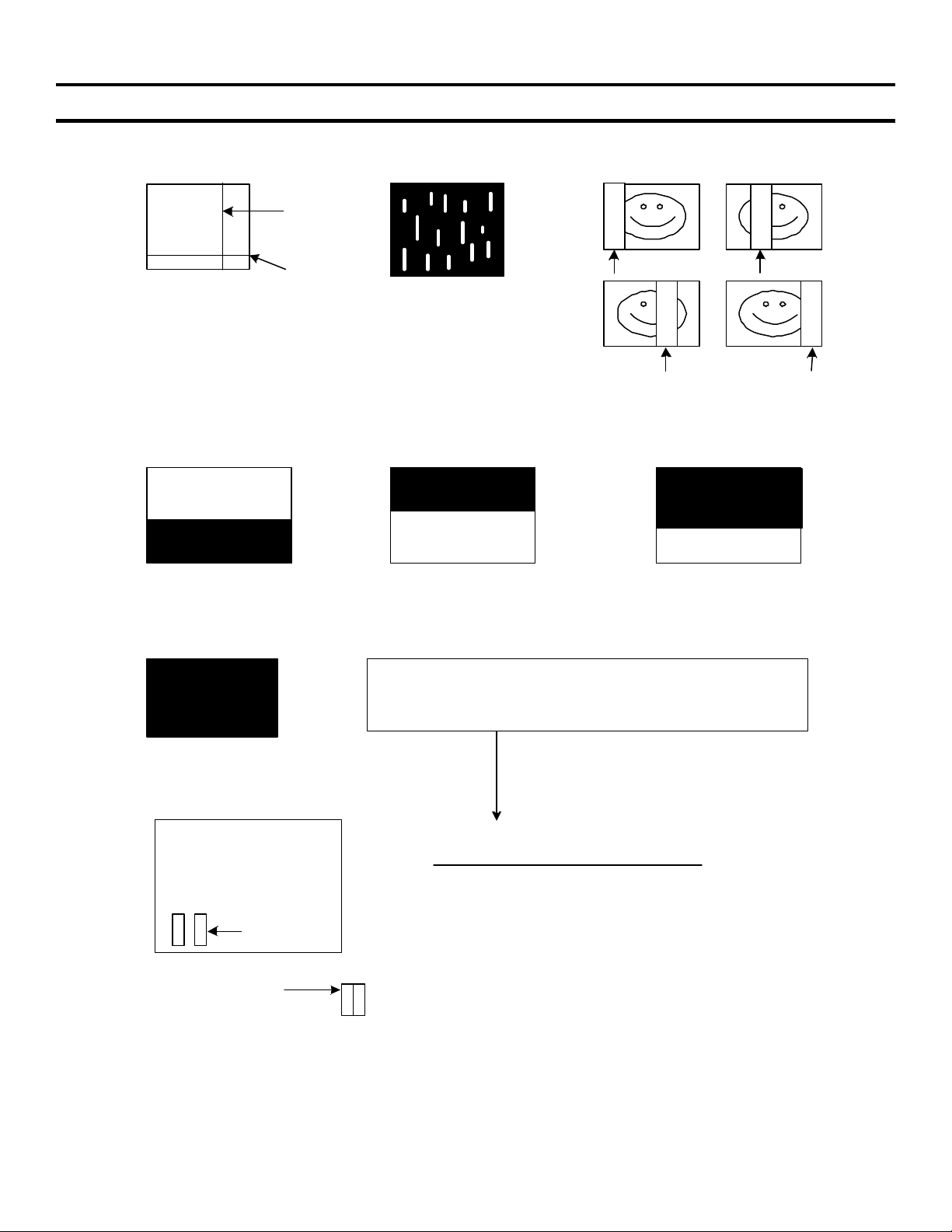
Board Location – Ref. Figure 4-1
V
a)
H
Vertical or
Horizontal
black / white
line through
the picture.
b)
Sony Model KZ-32TS1U // KZ-41TS1U TV Diagnostic Guide
c)
Colored rain
in a black
background.
White Noise
replaces 1/4
of the picture
d) e) f)
g)
Normal Pix
Black lower
half
Power Supply Board
CN 23
1
13, 15
gray wires
Normal Pix
Black upper
half
g) A Dark Screen with sound can be caused by the plasma
panel or the TV circuitry. Measure the DC voltages and signal
entering the plasma panel to determine which is defective.
Dark screen?
Check DC and signal video levels at CN23 & CN 1.
Normal Voltages with TV ON, any input
CN23/pin 1 = 55Vdc
CN23/pin 3 = 5Vdc
CN23/pin 8-10 = 78Vdc (32") or 82Vdc (42")
CN1/pins 13 & 15 (gray wires) = 1Vp-p @ 30MHz
If these input voltages/signals are OK, the plasma
panel is suspect. CN1 is on the plasma panel below
CN 1
1
the Power Supply board.
White noise
Black top, bottom
just white noise
5
Page 8
PLASMA
BOARD Y
5. Board Location
Chapter 5 - Board Location
POWER
SUPPLY
BOARD
PLASMA
BOARD X
B BOARD
Q BOARD
TU BD.
VHF
IN
FIGURE 5-1 - BOARD LOCATION - KZ-32TS1U
8TVP13 1444 4/10/02
6
Page 9
6. Service Mode
Figure 6-1
Chapter 6 - Service Mode
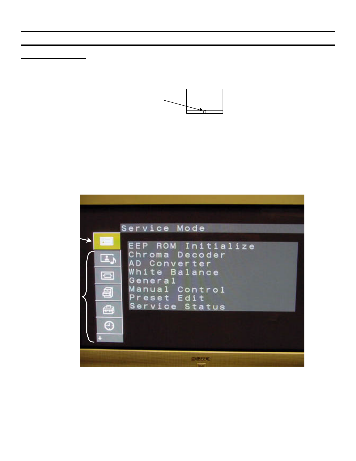
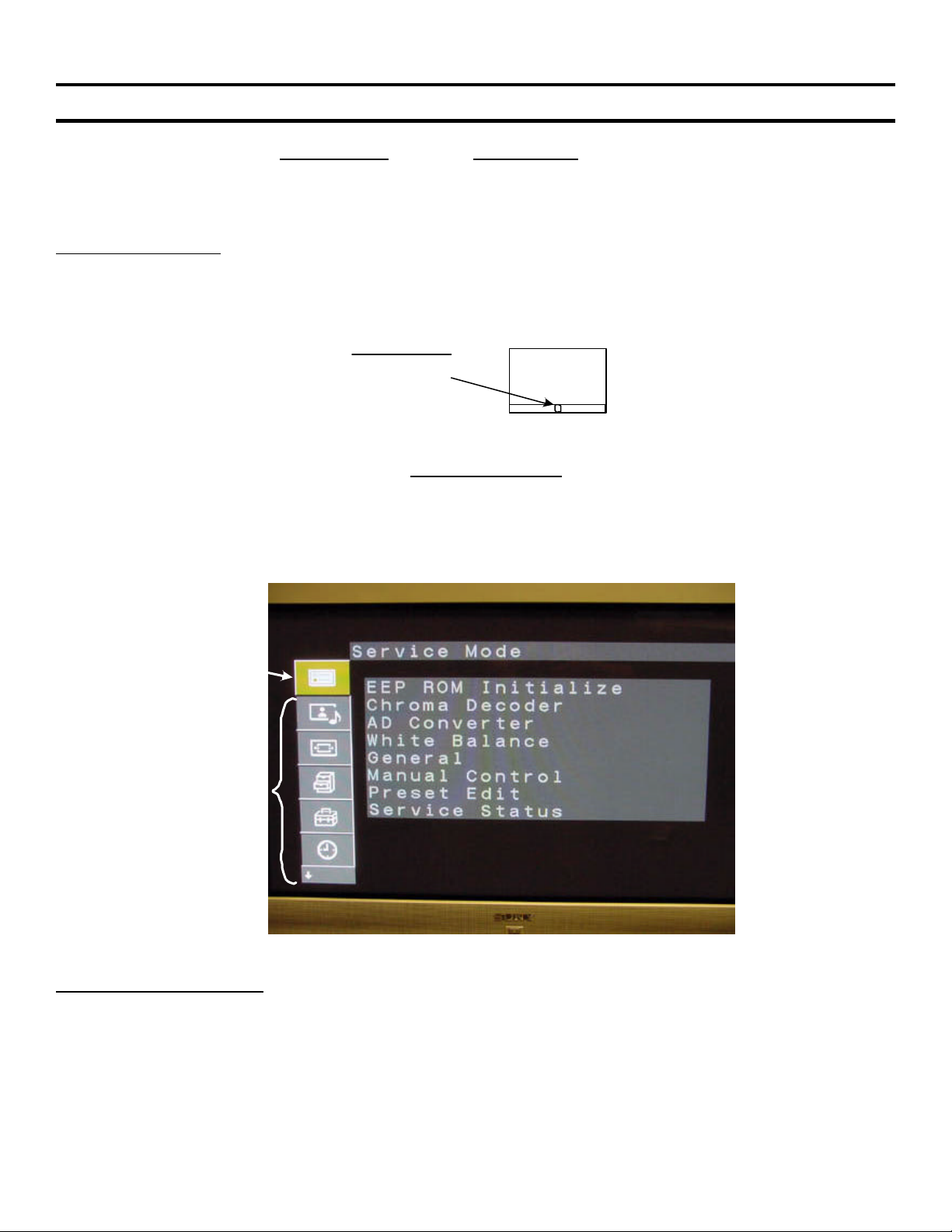
Service Mode Access
1. The TV must be in the Standby Mode as indicated by the front panel red light. Refer to Figure 6-1 for the
location of the standby light. If this Standby light is OFF, plug the TV into AC, press the front panel Power
button and then shut off the TV from the remote control. The Standby light should now be lit (red) while the
TV is OFF.
Standby/sleep
light
2. Using a Sony remote control aimed at the TV in the standby mode, quickly press: Display, 5, Volume +, Power
ON and MENU. If the TV turned ON when 5 was pressed, you did not press the next Volume + button fast
enough and will have to try again.
3. The following new service Mode menu shown in Figure 6-2 will appear above the user menu. Use the remote
control joystick to move and change the data as before. Store data as in previous service modes, by pressing
“Mute” and then “Enter”.
TV
Service
Menu
Normal
User
Menu
Figure 6-2 - Service Mode Display
7
Page 10
6. Service Mode
ial number, elapse operation time and diagnostic are erased.
= 8.
Service Mode Contents
Table 6-1 - Service Mode Contents
Service Category Contents
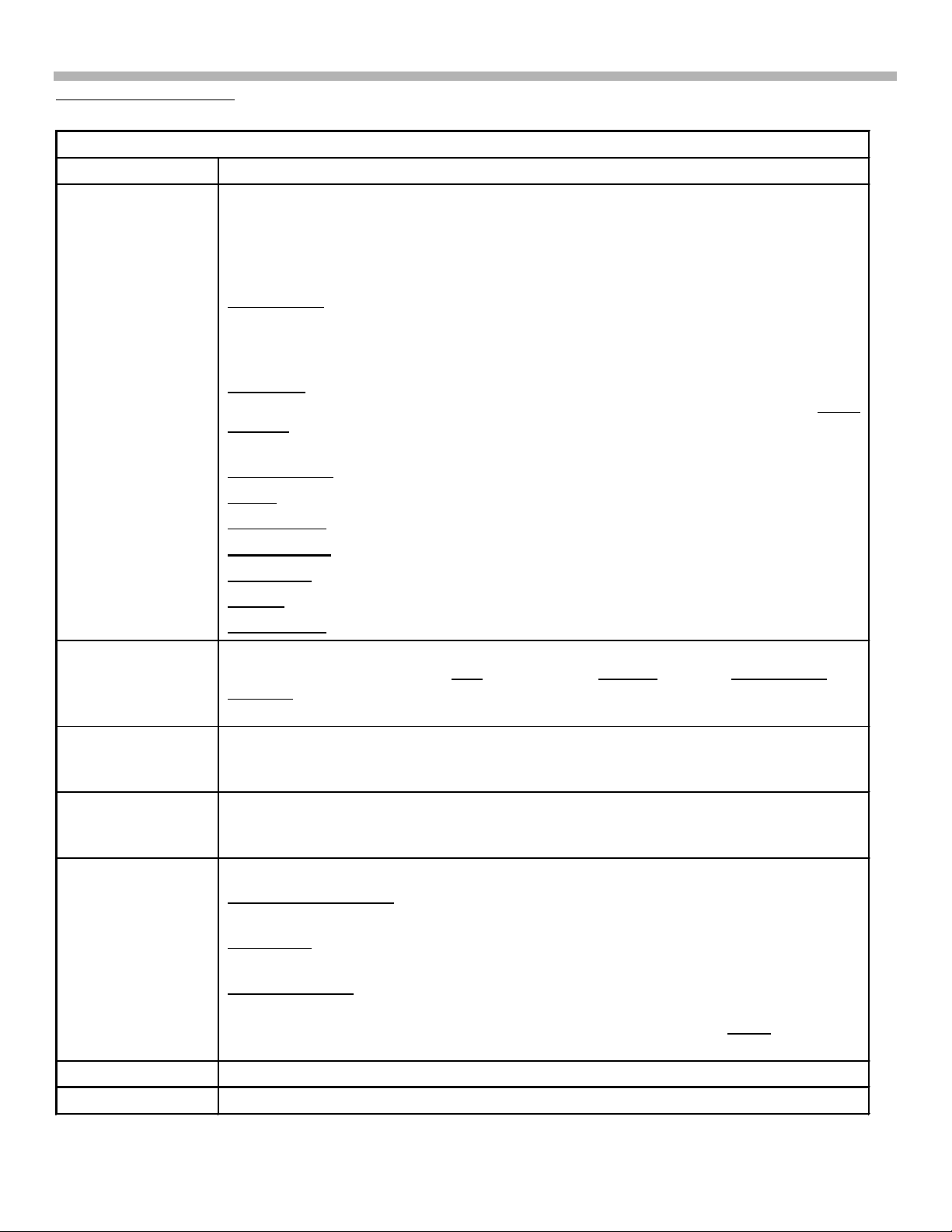
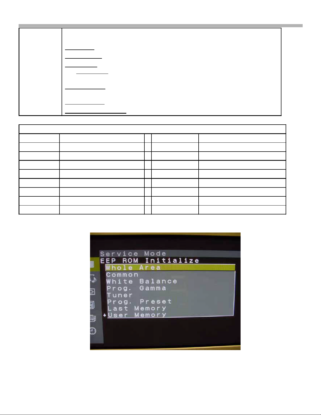
EEP ROM Initialize See Figure 6-3 for a list of Initialize contents. Selecting a line (like “Common”)
reveals two options: OK or cancel. Selecting OK stores default data and causes
the TV to reboot. You must press Menu when the TV turns back ON to return to
the service mode. Do not select OK unless you have read what you are resetting
to default levels.
Whole Area - Resets the entire EPROM and requires a full TV alignment
afterwards. The ser
This is used when the TV is made. For service, you can individually reset EPROM
contents:
Common - Resets items that are not signal related, such as: language, Orbit,
Diagnostic errors, serial number, color system and TV ON elapsed time. White
Balance – Resets Low, Mid and High Temperatures to midgain in preparation for
alignment after B board replacement.
Prog. Gamma - Is not used.
Tuner - Resets channels back to 2-13 and clears the Favorite channels.
Prog. Preset - Erases user station names.
Last Memory - Resets user video and audio preface settings.
User Mem – Is not used
Factory – Resets user settings to default except diagnostics and serial number.
Tuner Micom- Same as Tuner.
Chroma Decoder See Figure 6-4 for a content list. Preset contrast, sharpness, color and output levels
as shown in Figure 6-4. The Hue for NTSC = 8, Y Delay = 8, and Cb/Cr Offset
Sharp fo is the frequency the sharpness peaks. 0=2.5M, 1=3.2M, 2=4M, 3=off. Set
to 3.
AD Converter Adjust the brightness and hue for each input (video, component and RGB). Preset
these levels after the B board is replaced and touch up. See adjustments for the
procedure.
White Balance White balance adjustments at low, middle and high brightness levels. Preset these
levels after the B board is replaced and touch up. See adjustments for the
procedure.
General See Figure 6-5 for a content list.
AGC Wide & Narrow - Data affects capturing stations during auto programming
(wide = 14) and operation (Narrow = 13).
Fan Status - Displays the temperature of the power supply and the voltage applied
to the fan motor (8.6Vdc = slow).
Vs / Va Setting - The main plasma panel voltages Vs and Va are set using Uvrs
and Uvra. The 32” TV uses Uvrs = 82 and Uvra = 106. The 42” TV uses 93 and
128 respectively. Vs and Va needs adjustment if the logic board within the plasma
panel is replaced.
Manual Control See Figure 6-6 and 6-7. These are all preset to 00 except for: PDP =20.
Preset Edit See Figure 6-8. This section presets the parameters for a new video input signal.
8
Page 11
6. Service Mode
Service Status See Figure 6-9. This section displays the status of the input signal, and TV
condition.
Signal/sync - Format, freq, and sync polarity of the input signal.
Power Supply – Low voltage output of the power supply in voltage DC.
Fan & Temp - The fan voltage and power supply temperature. Within this category
is a No Ack Dev - Points to an IC that is not communicating with the Main Micro
using a 4-digit defect code number. See No Acknowledge Device table 6-2.
Warning Status – Shows completion of communications from the Main Micro (B
board) to memory IC and to 15 others.
Operation Time – Elapse TV ON time.
Software & PLD version – Software in Main micro and Panel Micro.
Table 6–2 - Service Mode - Service Status under Fan and Temp, No Acknowledge Device
Defect Code Suspected IC Defect Code Suspected IC
0001 Audio Processor (A board) 0002 Audio Switch (Q board)
0004 AV Switch IC (U board) 0008 V Chip (Q board)
0010 3D Comb filter IC (B board) 0020 Color Decoder (B board)
0040 Plasma Panel (PDP) 0080 Tuner (TU board)
0100 Auto Wide IC (B board) 0200 A/D Converter (B board)
0400 EPROM (M board) 0800 System IC (B board)
1000 V Chip (Q board) 2000 PLD (B board)
4000 Real Time Clock IC (B board) 8000 Scan Converter (B board)
Figure 6-3 Service Mode - EEP ROM Initialize
9
Page 12
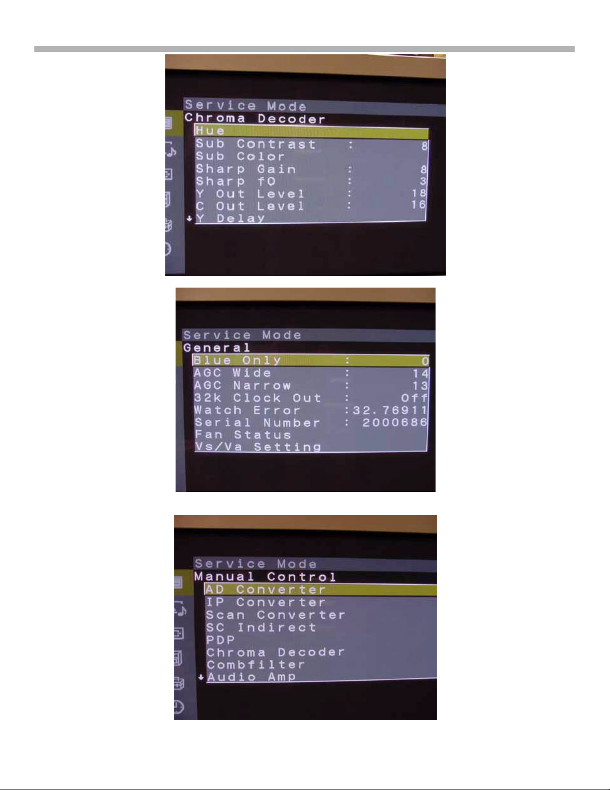
Figure 6-4 Service Mode – Chroma Decoder
6. Service Mode
Figure 6-5 Service Mode –General
Figure 6-6 Service Mode – Manual Control 1/2
10
Page 13
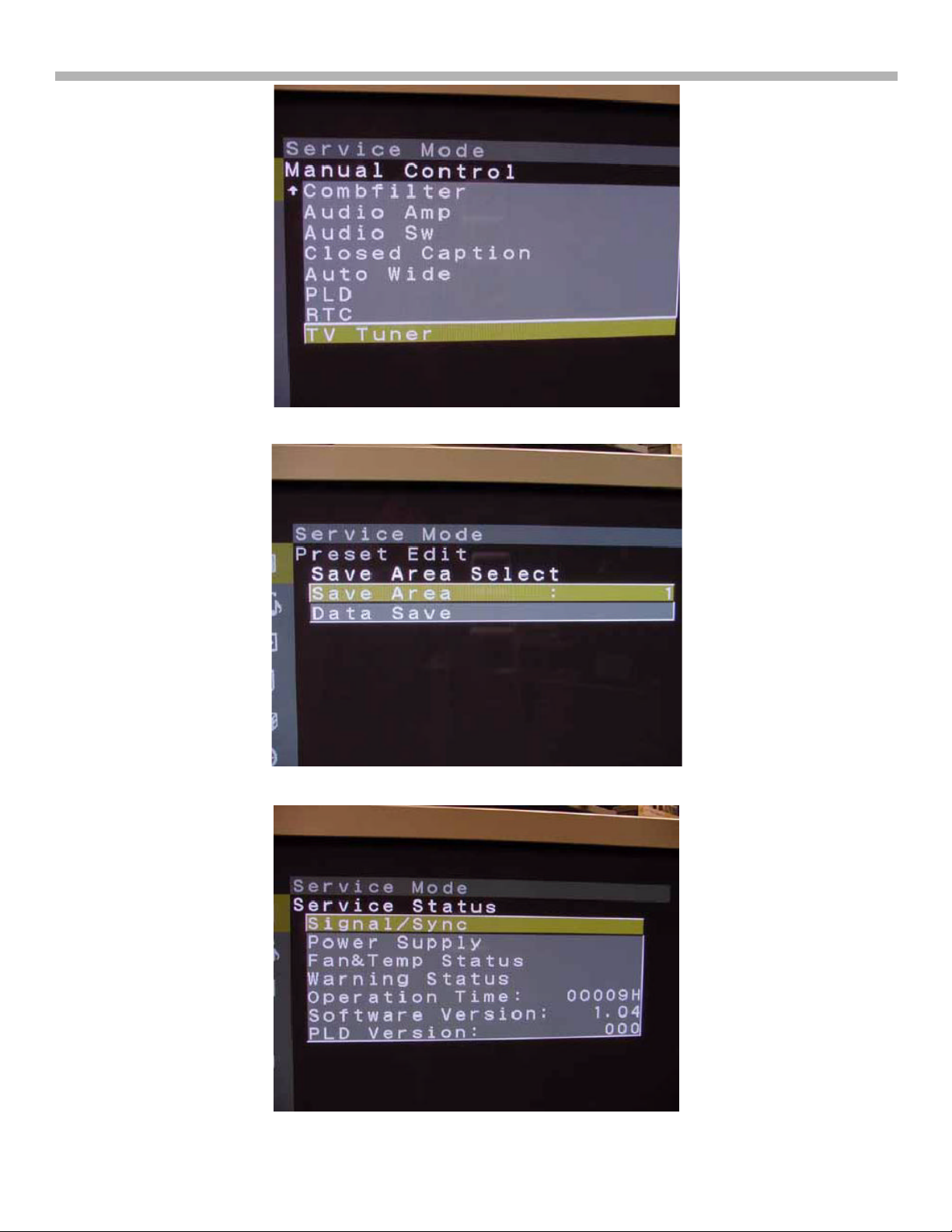
Figure 6-7 Service Mode – Manual Control 2/2
6. Service Mode
Figure 6-8 Service Mode –Preset Edit
Figure 6-9 Service Mode –Service Status
11
Page 14
7. Adjustments when the B Board Needs to be Replaced
Chapter 7 - Adjustments when the B Board is Replaced
If the B board is replaced, the A/D Converter levels and white balance need to be adjusted or the brightness and
tint range will not be consistent when switching inputs. These settings are made from the service mode for each
input (Tuner, Video and Component) type and the data is saved in a NVM IC on the TV’s B board.
Service Mode Access
1. The TV must be in the Standby Mode as indicated by the front panel light. If this Standby light is OFF, plug
the TV into AC, press the front panel Power button and then shut off the TV from the remote control. The
Standby light should now be lit while the TV is OFF. Ref. Figure 7-1.
Standby Mode
Standby/sleep
light must be
red
Figure 7-1
TV
2. Using a Sony remote control aimed at the TV in the standby mode, press: Display, 5, Volume +, Power ON and
MENU, quickly. If the TV turned ON when 5 was pressed, you did not press the next Volume + button fast
enough and will have to try again.
3. The following new service Mode menu shown in figure 7-2 will appear above the normal user menu. Use the
remote control joystick to move and change the data as before. Store the new data by pressing Mute, and then
Enter, as before.
Service
Menu
Normal
User
Menu
Figure 7-2 - Service Mode Display
A/D Converter Adjustments
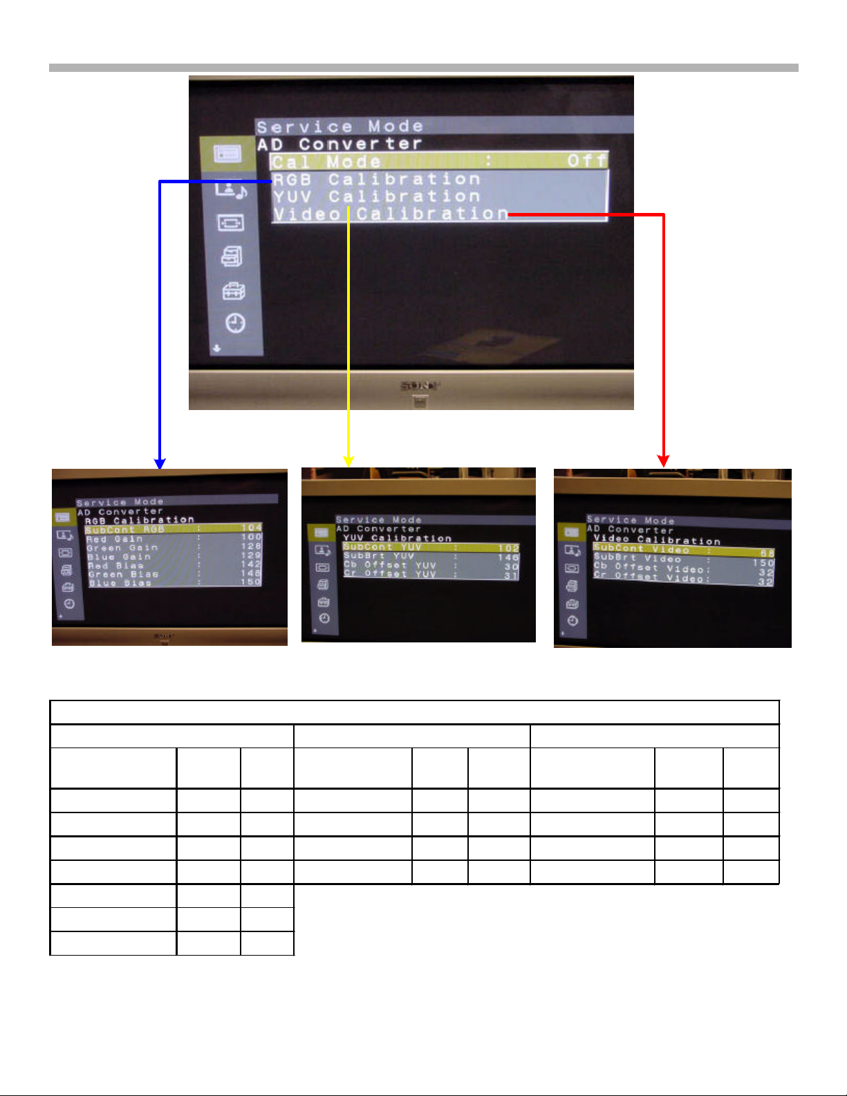
White balance and brightness levels for the three types of video inputs are set in the AD Converter area of the
service mode. All three types of video inputs (RGB, YUV and Video) are shown in Figure 7-3 and Table 7-1.
Adjust each one by feeding the corresponding white input to the back of the TV or temporally preset them to
these default values shown. Use the remote control joystick to select and change the data.
12
Page 15
7. Adjustments when the B Board Needs to be Replaced
`
Figure 7-3 - A/D Converter Preset Default Levels
3/13/02
Table 7-1 A/D Converter (WB & Brightness) Default Levels
RGB YUV (Component Video) Video (Composite Video)
Item 32”
Level
42”
Level
Item Level 42”
Level
Item Level 42”
Level
Sub Cont RGB 104 110 SubCont YUV 102 106 SubCont Video 68 65
Red Gain 100 114 Sub Bri YUV 146 145 SubBrt Video 150 142
Green Gain 128 128 Cb Offset YUV 30 31 Cb Offset Video 32 34
Blue Gain 129 131 Cr Offset YUV 31 31 Cr Offset Video 32 34
Red Bias 142 139
Green Bias 148 147
Blue Bias 150 150
13
Page 16
7. Adjustments when the B Board Needs to be Replaced
LEVELS - MODEL KZ-32TS1U
White Balance
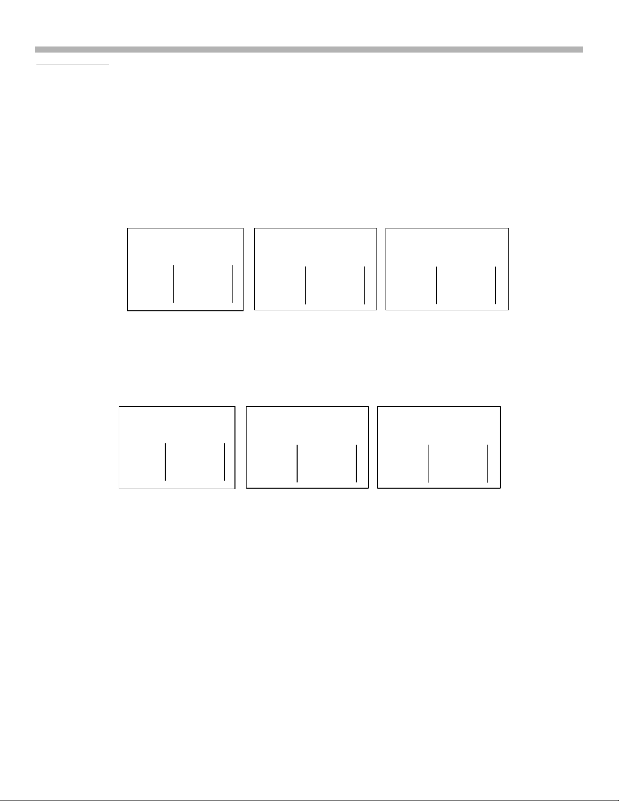
In the service mode, you will preset the RGB gain levels for the High, Middle and Low color temperatures, then
check the white balance as brightness is increased from minimum to maximum. Figure 7-4 Shows the RGB
levels for the 32" TV and Figure 7-5 shows the levels for the 42" TV. Use the remote control joystick to select and
change the data (position of the x). Store the data by pressing “Mute” and then “Enter”.
Check the white balance as you increase the TV’s brightness level bar from low to middle to high screen brightness.
The white areas of the picture should remain white even as the brightness is changed. If the white balance is off,
return to the stop service mode and touch up the R, G or B adjustment level.
KZ32TS1U
Figure 7-4 shows the White Balance levels from a 32" Plasma TV.
White Balance
Color Temp: High
R
G
B
X
X
X
White Balance
Color Temp: Mid
R
G
B
X
X
X
FIGURE 7-4 - WHITE BALANCE PRESET DEFAULT
KZ-42TS1U
Figure 7-5 shows the White Balance levels from a 42" Plasma TV:
White Balance
Color Temp: High
R
G
B
X
X
X
White Balance
Color Temp: Mid
R
G
B
X
X
X
FIGURE 7-5 - WHITE BALANCE PRESET DEFAULT
LEVELS - MODEL KZ-42TS1U
White Balance
Color Temp: Low
R
G
B
White Balance
Color Temp: Low
R
G
B
X
X
X
X
X
X
14
Page 17
8. Plasma Panel Replacement - KZ-32TS1U
Chapter 8 - Plasma Panel Replacement - KZ-32TS1U
The KZ-32TS1U and the KZ-42TS1U are mechanically different and have separate procedures for removal
of the Plasma Panel.
Handling Precautions
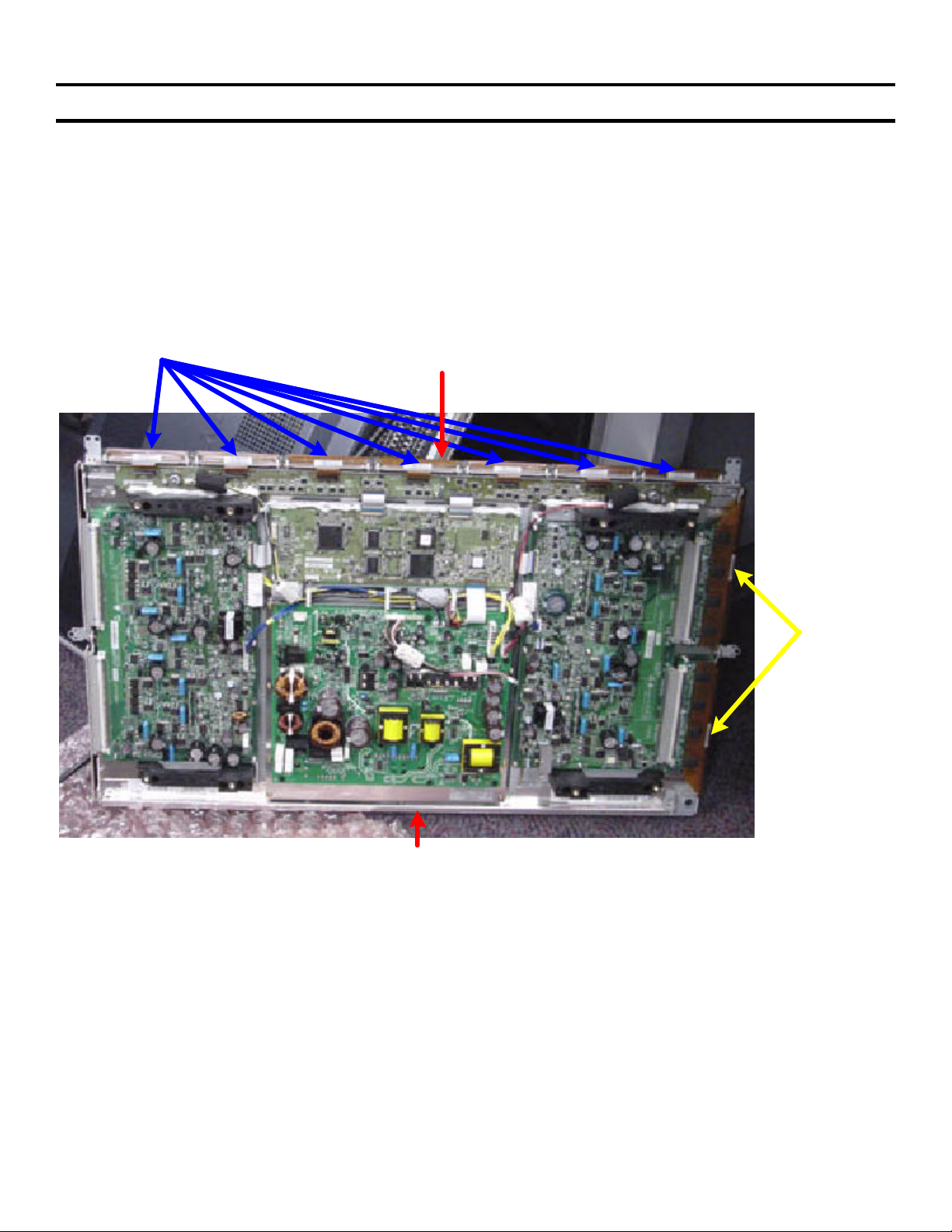
After removing the plasma panel from the TV, note that there are flex cables located at the bottom and both sides
of the panel that are susceptible to damage.
So the flex cables are not damaged, only rest the plasma panel topside down as shown in figure 8-1.
Bottom
Flex Cables
Panel
Bottom
Flex
Cables
Top
Figure 8-1 - Plasma Panel Standing Upside Down
Procedure – KZ32TS1U
In the steps to follow, you will remove the rear panel, the shield, the board assembly and both support rails to free
the plasma screen that is connected to the front bezel.
15
Page 18
Fan & Shield
Ÿ Remove
8. Plasma Panel Replacement - KZ-32TS1U
Figure 8-2 - Back Removed
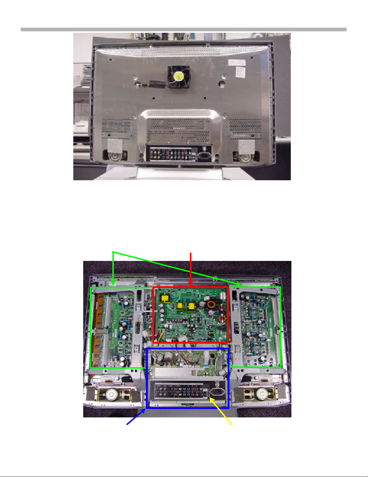
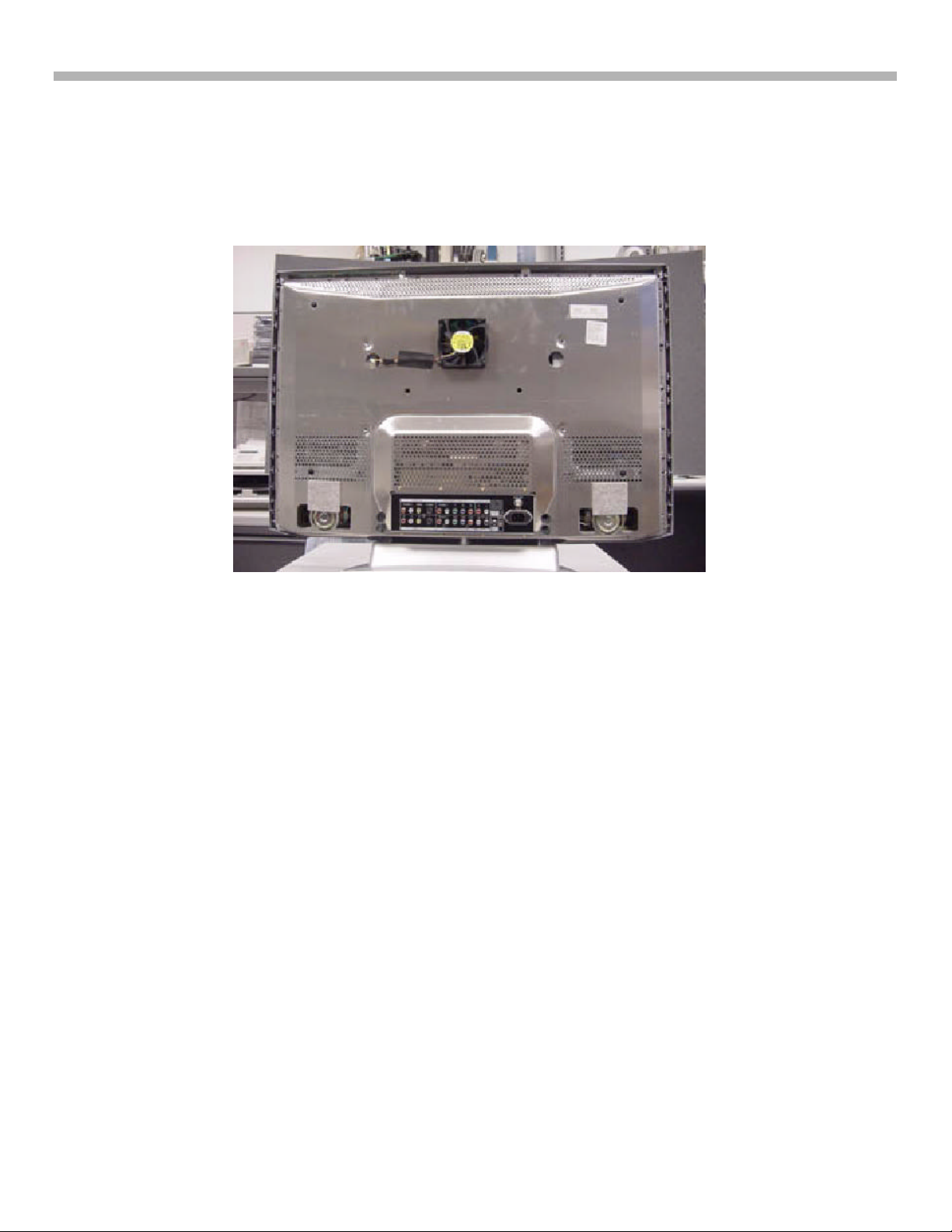
a) Begin by removing the back panel to expose the shield, shown in figure 8-2.
b) Unplug the fan and remove the shield.
Plasma
Panel
Power
Supply Board
Lower
Board Assembly
Board
Layout
Figure 8-3 - Circuit Boards
16
TV Board
Assembly
Page 19
8. Plasma Panel Replacement - KZ-32TS1U
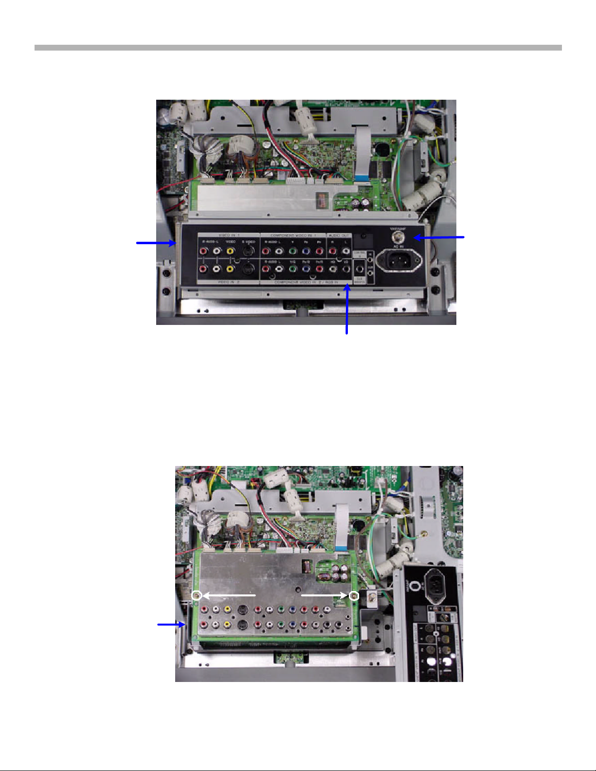
Figure 8-4 - Input Panel
The lower board assembly (behind the input jacks) must be removed because the plasma panel cannot be slid
out from underneath it. There is a lip under the board assembly that prevents the panel from being slid sideways.
c) Remove the input connector cover (four screws + VHF input jack)
TV
Board
Assembly
Ÿ Remove the
Input Connector
Cover
Input
Connector Cover
Screw
The TV boards are in an assembly held in by four black screws. Two can be easily seen at the right in Figure 8-
5. The left two are behind the plate. In the next three steps, you will lower the front Q board to remove all the
screws and pull out the H1 board cable harness from the assembly.
d) Remove two screws holding the front Q board in the TV board assembly (see Figure 8-5). Fold it down.
e) Remove the four black screws holding the TV board assembly. Gradually pull the assembly toward you.
f) Snake the H1 Board cable harness out the back to free the TV board assembly (see Figure 8-6).
2 Screws
Plate
Remove TV Board Assembly 1
Ÿ Fold Down board
Figure 8-5 - Remove TV Board Assembly 1
17
Page 20
Remove the TV Board Assembly 2
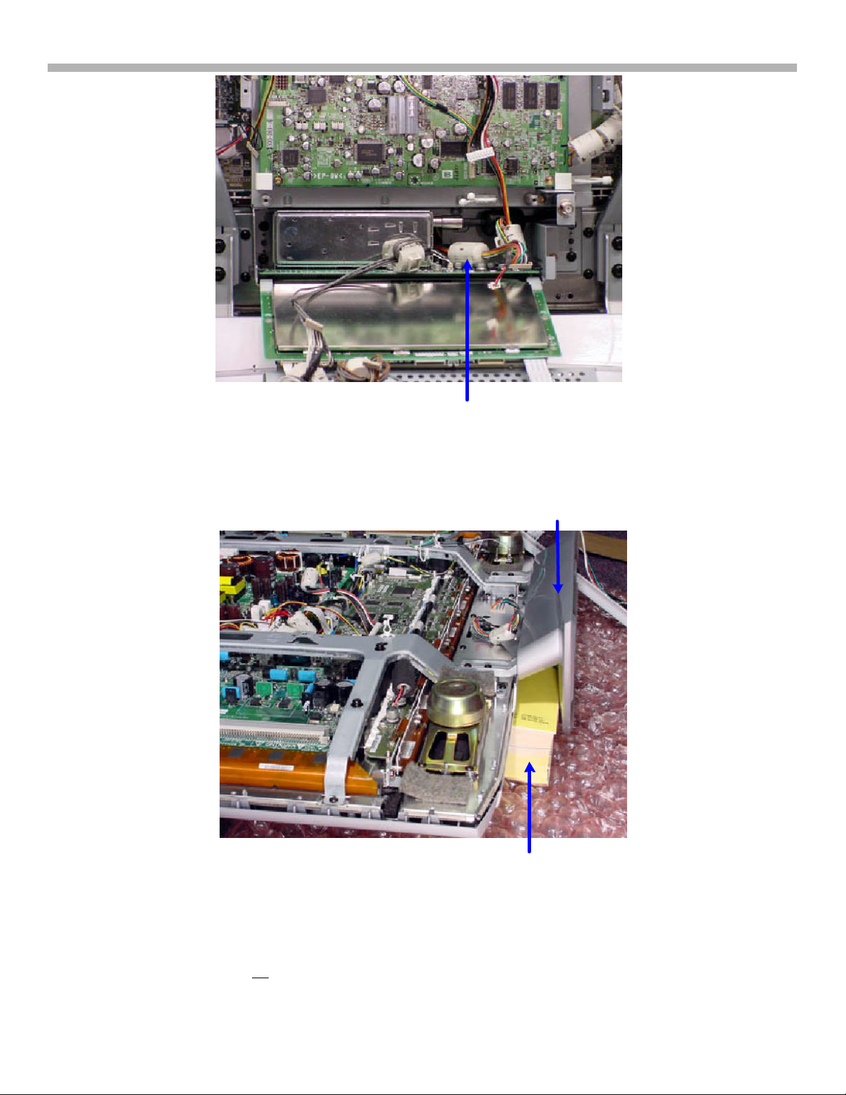
Figure 8-6 - Remove TV Board Assembly 2
Phone
Ÿ Snake the H1 board harness out
the back hole
8. Plasma Panel Replacement - KZ-32TS1U
H1 Board
Cable
Harness
In the next two steps, the TV must be supported while face down and the base removed.
Book(s)
Ÿ Insert Books
Figure 8-7 - Base Removal 1
Phone
Book(s)
g) Lay the TV face down on a clean soft cloth. Bubble wrap was used in these pictures because it was clean
and soft.
h) Use books to lift the base off the floor.
18
Page 21
Top View
8. Plasma Panel Replacement - KZ-32TS1U
Support
Brackets
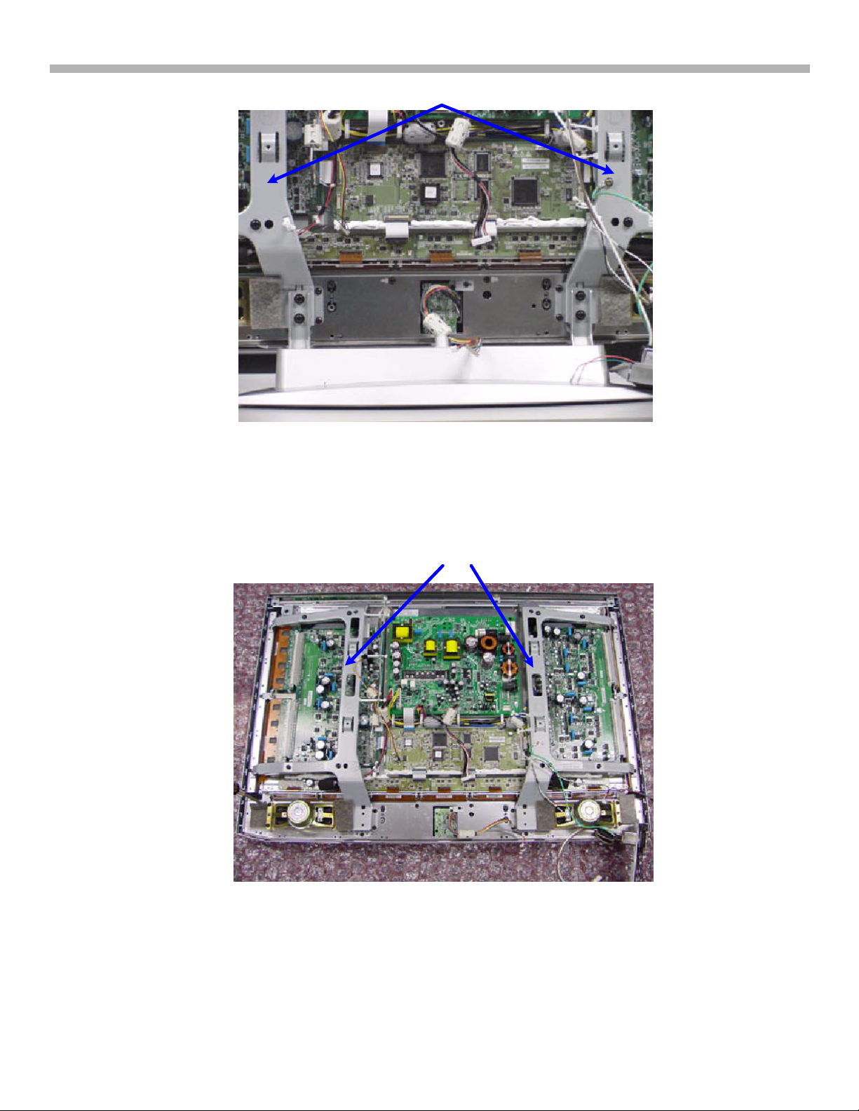
Figure 8-8 - Base Removal 1
i) Remove the base.
j) Lay the TV screen flat on the floor.
Bezel, P.S and Plasma Screen
Ÿ Remove bracket
Support
Brackets
Figure 8-9 - Base Removal 2
k) Remove the two support brackets.
19
Page 22
8. Plasma Panel Replacement - KZ-32TS1U
Figure 8-11 - Plasma Panel Standing Upside Down
Handles
Figure 8-10 - Plasma Screen Handles
Power Supply
Board
Handles
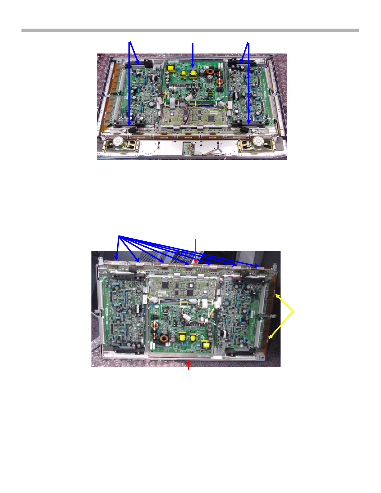
l) Finally, remove the plasma screen – use the four black handles to lift. Only place the top of the plasma
screen down. The other three sides have vulnerable flex cables present.
Bottom
Flex Cables
Panel
Bottom
Top
m) Remove the power supply board (mounted on the larger metal heat sink).
Flex
Cables
20
Page 23
8. Plasma Panel Replacement - KZ-32TS1U
`
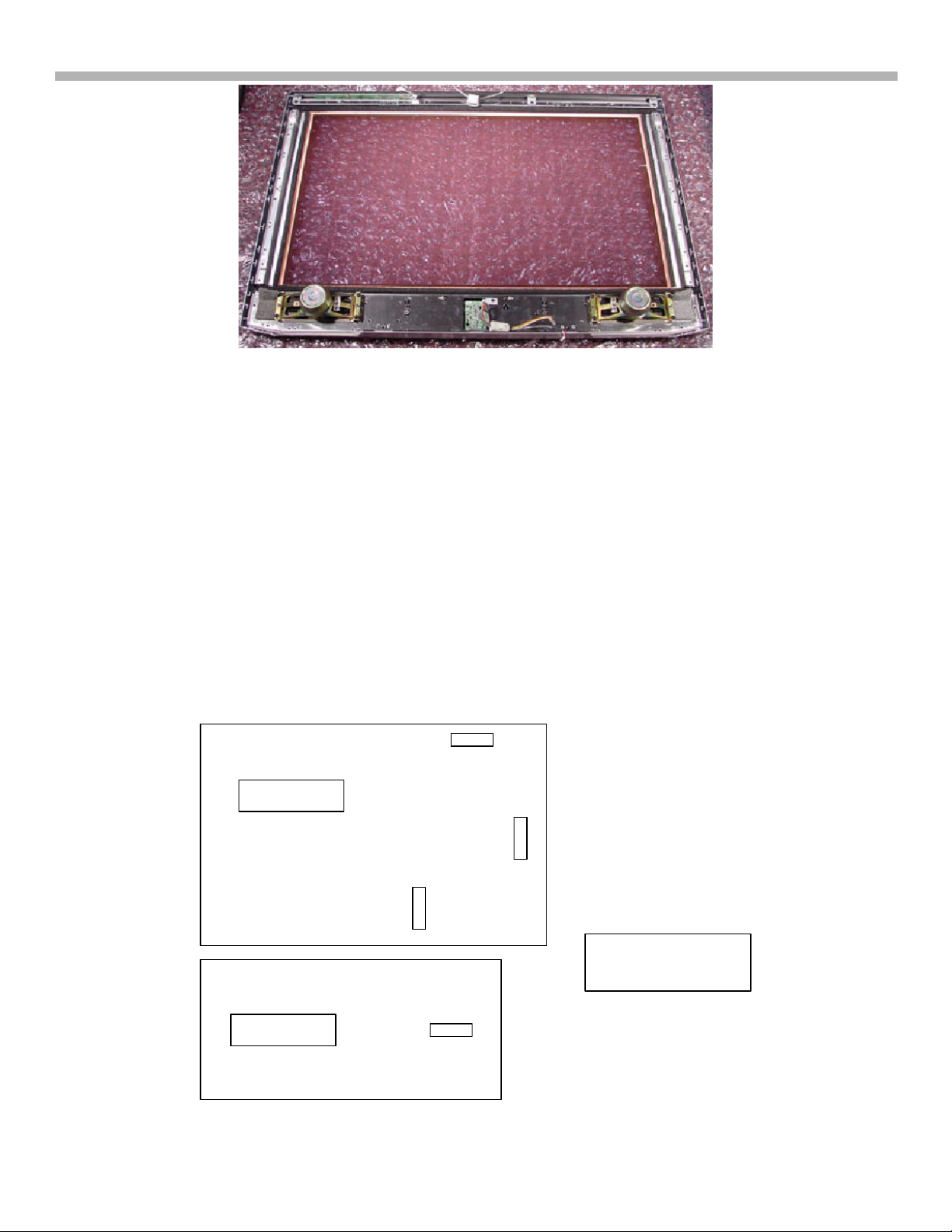
Figure 8-12 - Front Glass Screen
n) The inside of the TV screen is coated so do not clean or leave oil on it by touching it. The inside surface
scratches easily. Clean the inside of the TV screen if there is film or fingerprints. Use the Sony p/n X-4034197-1 soft cloth and diluted mild window cleaner if necessary. A 50% mix of water and window cleaner is OK.
Do not use dishwashing detergent or soaps.
Reassembly
Assemble in the reverse order:
• Screw the power supply board onto the Plasma Panel (Figure 8-10).
• Position the Plasma Panel into bezel (Figure 8-10).
• Fasten left and right support brackets over the handles (Figure 8-9).
• Snake the H1 board cable harness into the TV board assembly rear and secure the assembly (Figures 8-6 &
8-8).
• Plug in the connectors. Make sure these test connectors on the B and Q boards are empty (Figure 8-13
shows the location of empty CN1003, CN1002, CN1201 and CN3008).
CN1003
B Board
CN1002
CN1201
Figure 8-13 - Unused
Test Connectors
Q Board
CN3008
21
Page 24
8. Plasma Panel Replacement - KZ-32TS1U
• Mount the input connector cover that contains the AC socket (Figure 8-3).
• Test the TV by plugging in AC and a VHF signal. The TV will operate for at least 30 minutes without the fan
connected. There will be horizontal noise bars of interference from the power supply when the rear shield is
not installed.
• Install the TV shield and fan. Make sure the shield makes contact to the conductive mesh on all four
sides and the shield is screwed into the center TV board assembly or you will have interference on
the TV stations.
• Install the rear panel.
Fan & Shield
Figure 8-2
22
Page 25
9. Plasma Panel Replacement - KZ-42TS1U
FIGURE 9-2 - BACK WIRES
Chapter 9 - Plasma Panel Replacement - KZ-42TS1U
The KZ-32TS1U and the KZ-42TS1U are mechanically different and have separate procedures for the Plasma
Panel removal.
Handling Precautions
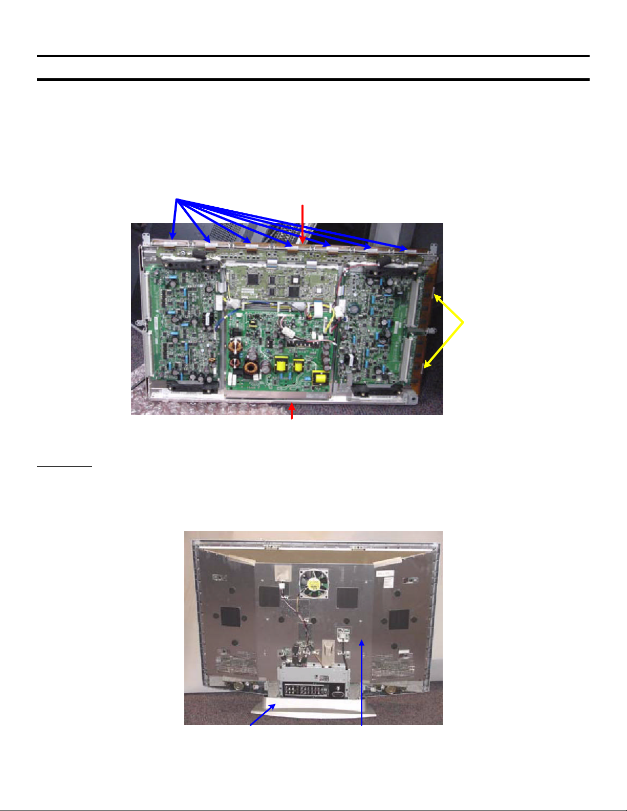
• After removing the plasma panel from the TV, note that there are flex cables located at the bottom and both
sides of the panel that are susceptible to damage. Only rest the plasma panel topside down so the cables
are not damaged. The 32" Plasma panel is shown. The 42" is similar.
Bottom
Flex Cables
Panel
Bottom
Flex
Cables
Top
Figure 9-1 - Plasma Panel Standing Upside Down
Procedure:
In the following pictured steps, you will remove the rear circuit board assembly and the rear shield.
Before you can pull off the plasma panel:
a) Remove the back panel to expose the input circuit board assembly and shield.
Circuit Board
Assembly
Shield
23
Page 26
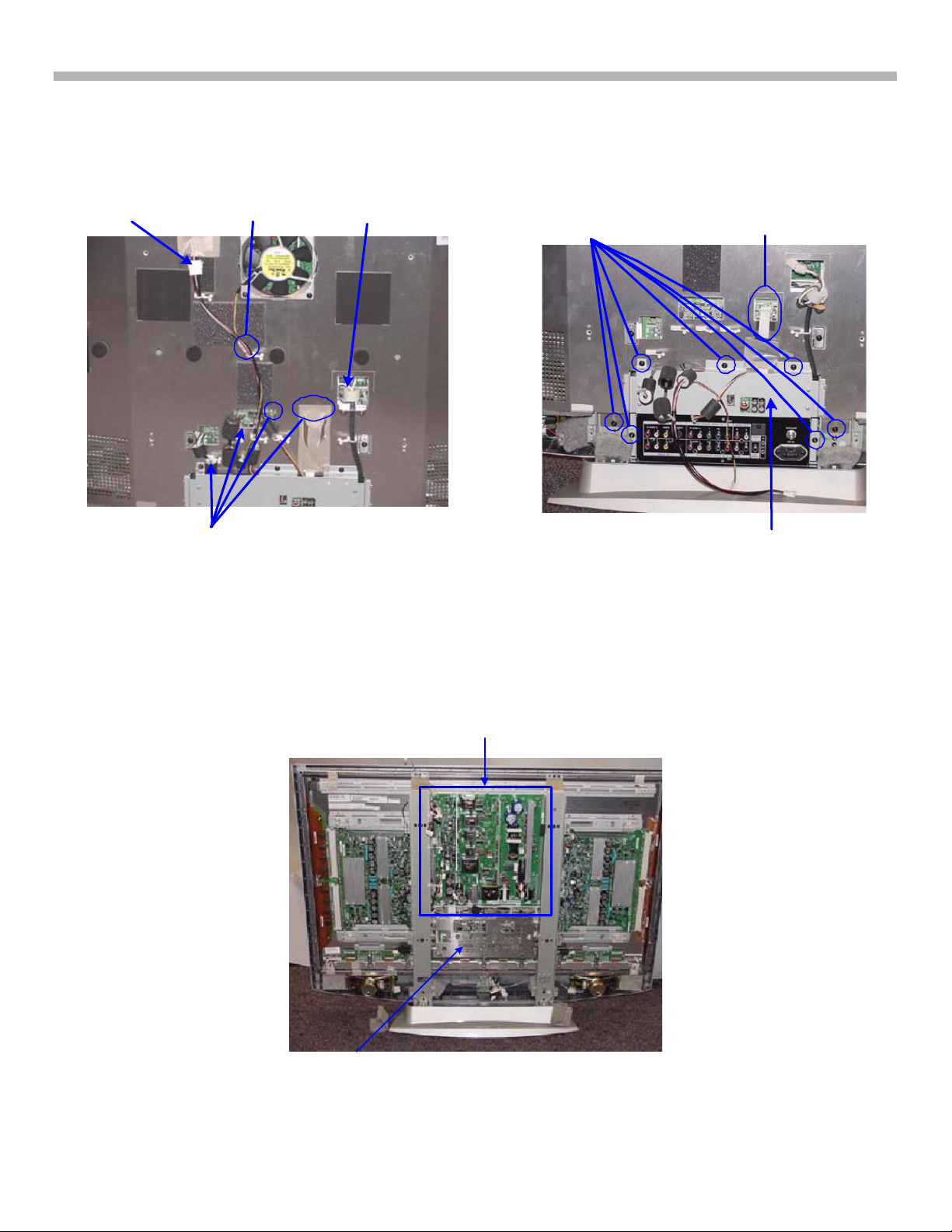
9. Plasma Panel Replacement - KZ-42TS1U
b) Seven connectors must be removed. Three connectors have a catch that must be pulled or squeezed to
separate the connector. The remaining four connectors are simply unplugged. Remove the conductive
mesh tape that shields the ribbon connector and unplug the white ribbon cable (Figure 9-3) by pulling it
straight out. Do not fold the ribbon cable.
Squeeze
Connector
Pull Catch
Connector
Unplug
Connector
Squeeze
Connector
7 Machine
Screws
Ribbon Cable
behind the tape
Circuit Board
Assembly
FIGURE 9-3 - REMOVE 7 CONNECTORS AND 7 SCREWS
c) Remove the seven machine screws around the circuit board assembly and pull off the assembly.
d) Remove the rear shield with the top decorative panel to expose the circuitry (Figure 9-4).
Power
Supply
B Board
FIGURE 9-4 - REAR SHIELD REMOVED
24
Page 27
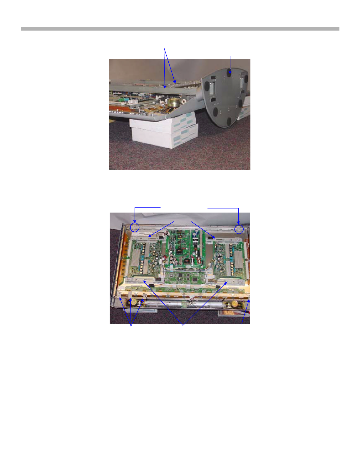
e) Place the TV face down on some books so the TV is level.
Conductive
Mesh Tape
Rails
B Board
FIGURE 9-5 - LEVEL THE TV ON BOOKS
f) Remove the two rails with the center B board and TV stand.
9. Plasma Panel Replacement - KZ-42TS1U
Stand
Conductive Mesh Tape
Handles
Conductive
Mesh Tape
FIGURE 9-6 - RAILS AND STAND REMOVED
Handles
g) Mark the position of the conductive mesh tape around the plasma panel before removing them. They are
necessary to prevent interference on the screen.
h) With a partner, lift the plasma screen off by the handles (Figure 9-6). PLACE THE PANEL UPSIDE DOWN
ON THE FLOOR – SEE FIGURE 9-7. The power supply board must be removed from the panel if the panel
is to be replaced. Only clean the inside of the screen with Sony cloth p/n X-4034-197-1.
25
Page 28
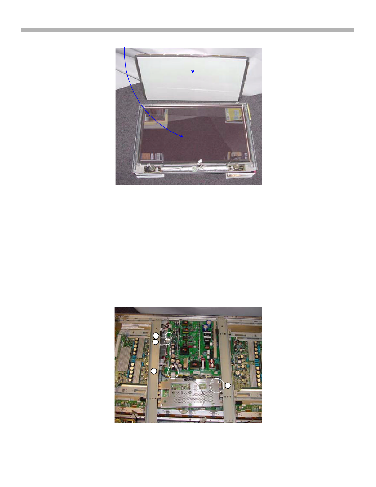
9. Plasma Panel Replacement - KZ-42TS1U
Reassembly
In the reverse order of removal:
Glass
Screen
FIGURE 9-7 - SCREEN UPSIDE DOWN ON FLOOR
Plasma Panel
Bottom
Top
• The inside of the TV screen is coated so do not clean or leave oil on it by touching it. The inside surface
scratches easily. Clean the inside of the TV screen if there is film or fingerprints. Use the Sony p/n X-4034197-1 soft cloth and diluted mild window cleaner if necessary. A 50% mix of water and window cleaner is OK.
Do not use dishwashing detergent or soaps.
• Place the screen in the bezel.
• Mount the rails, B board and stand.
• Plug in four connectors from the B board into the plasma panel as shown in Figure 9-8. CN9004 next to
connector 2 is not used. The fourth connector is under the B board.
Reattach these 4 connectors
1
2
3
4
FIGURE 9-8 - ATTACH 4 CONNECTORS
26
Page 29

9. Plasma Panel Replacement - KZ-42TS1U
• Attach the conductive mesh tape between the bezel and plasma panel (refer to Figure 9-6).
• If you want to test the TV before installing the shield, attach the rear circuit board assembly, plug it in and turn
on the TV set. Without the rear shield in place, you will get horizontal lines of interference on the TV channels
from the power supply. After testing, remove the rear circuit board assembly to install the shield.
• Install the rear shield with the decorative top control panel. Put the top ferrite assembly inside the shield or
you will not be able to fasten the rear cover later on. Make sure the shield mates with the metal on all four
sides to complete the shield.
• Attach the rear circuit board assembly.
• Replace the two conductive mesh tapes over the upper and lower holes in the rear shield (refer to Figure 9-
2).
• Put the back cover in place
27
Page 30
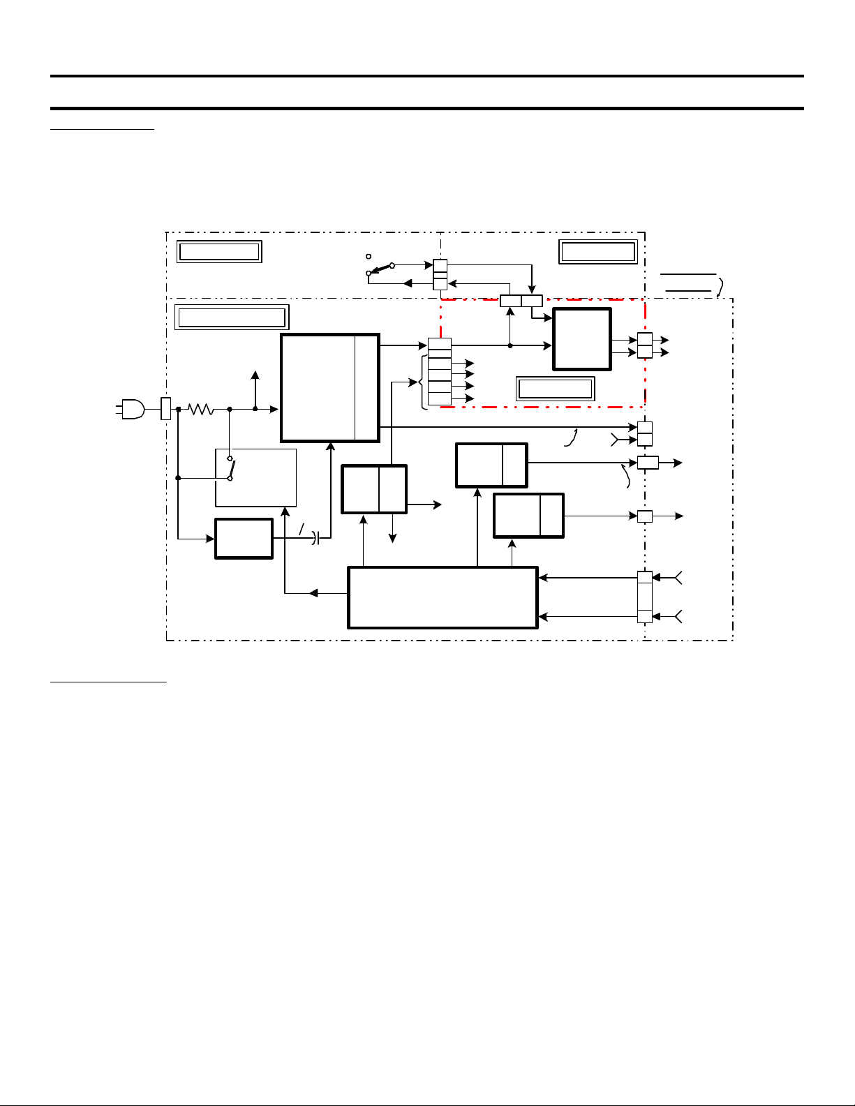
Chapter 10 - Standby Power / Power ON
Standby Power
Standby power is present when:
• The TV is plugged in.
• The front panel ON/OFF switch is latched in.
• The red standby light within the ON/OFF button is lit.
10. Standby Power / Power ON
H1 BOARD
PWR SUPP.BD.
T2,T4,T5
RY1
SURGE
RELAY
IC1
REG.
TV OFF
ON
IC10
STANDBY
POWER
6V
+
C16
10
S4101
T1
IC11
PS3
CN3005/5,8
9,10
CN1/CN101
T2
CN6/6
IC21, IC22
CONTROL
CN4100/CN3006
2
1
30 24
STBY
5V
1
5,6
13
15
3.3V
5V
6V
13V
IC13
PS1
T4
IC15
PS2
Q BOARD
CN3003/
CN1001
IC1004
ON
MAIN
B BOARD
STBY
3.3V
T5
3.2V =TV ON
0V =TV OFF
CPU
T2
32"=78V
42"=82V
54.5V
CN
1203/
CN1
PLASMA
PANEL
CPU_GO
5
= 3.2V
6
RDP_GO
= 3.2V
CN6
1
STBY 3.3V
6
5V
7-9
CN33
CN23
1
CN7
6
8
Vs
VA
VSA
GO
VCE
GO
FIGURE 10-1 - POWER ON
1TVP13 1431 3/14/02
Circuit Operation
Refer to Figure 10-1. The standby power must be kick-started by a 6V pulse available when the TV is first
plugged into AC. The 6V pulse comes from regulator IC1 and passes through C16 into the standby power supply
circuit. Within the standby power supply is IC10 and T1. IC10 is an oscillator that starts and feeds small
transformer T1. T1 outputs standby 5Vdc to the Micro CPU (B board) and standby 3.3Vdc to the plasma panel.
Another T1 output (not shown) supplies voltage to the + end of C16 to keep the standby power supply ON after
the kick-start pulse had decayed. Therefore, the standby power supply starts and runs as long as the TV is
plugged into AC, regardless of the TV’s Power ON switch position.
Power ON
Power ON can be initiated only after the front panel Power ON button has been pressed (S4101 closed on the Q
board), causing the red Standby light beneath this button to light (standby 5Vdc present). See figure 10-1. This
switch closure releases Micro CPU IC1004 (B board), permitting IC1004 to turn ON the TV.
Then the TV may be turned ON:
• From the front panel by pressing the channel + or – buttons.
• From the front panel by pressing the Power ON button twice.
• From the remote by pressing the channel + or – buttons, or the individual channel numbers.
• From the remote by pressing the Power ON button.
28
Page 31
10. Standby Power / Power ON
Circuit Operation
Once standby power is available to the Micro CPU IC1004 (B board), IC1004 can respond to either the channel
buttons or power ON button to turn ON the TV. Two commands are output IC1004 to turn ON the Plasma panel.
CPU_GO and RDP_GO both go high at CN1/pins 5 and 6.
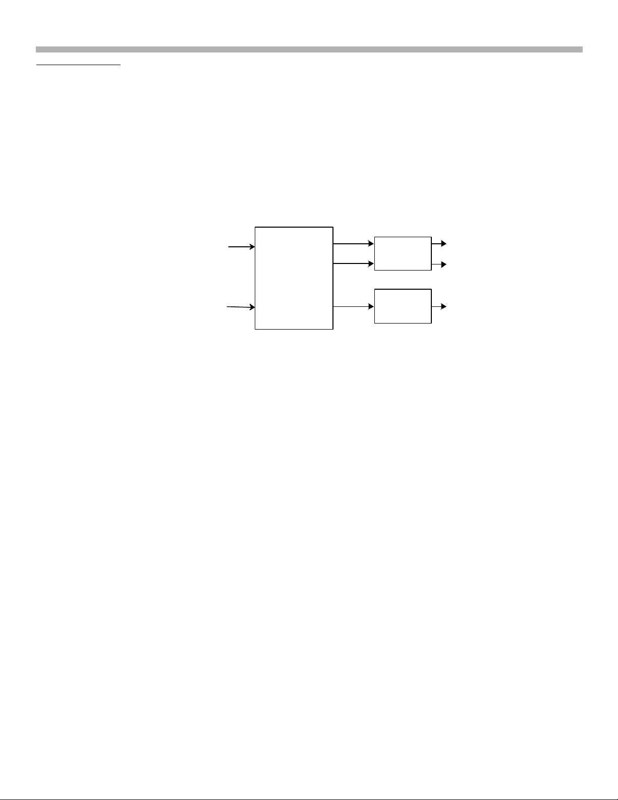
The power ON path has to go through the plasma panel. After the panel has initialized, it will output two commands
to turn ON the remainder of the power supply and energize the surge relay. These commands are VSA_GO and
VCE_GO from CN 7/pins 6 and 8. When both of these two commands go HIGH, the power supply outputs the
remainder of the voltages and the TV turns ON. Within the power supply board, three separate regulated
supplies reside (PS1, PS2 and PS3). As shown in Figure 10-2. these power supplies feed output transformers
T4, T5 and T2, respectively. T4 outputs the Vs (sustain driver) voltage and T5 outputs the Va (address driver)
voltage for the plasma panel. The remainder of the TV voltages come from T2.
Power supply
power ON =
3.2Vdc from
Plasma panel
CN 7/pins 6, 8
VSA_GO
CN 7/pin 6
VCE_GO
CN 7/pin 8
Control
IC21, IC22
----------------
PS 1 (T4)
PS 2 (T5)
PS 3 (T2)
FIGURE 10-2 - POWER SUPPLY CONTROL CONCEPT
Vs
Va
TV Voltages
4/16/02
29
Page 32
11. Fan Operation
Chapter 11 - Fan Operation
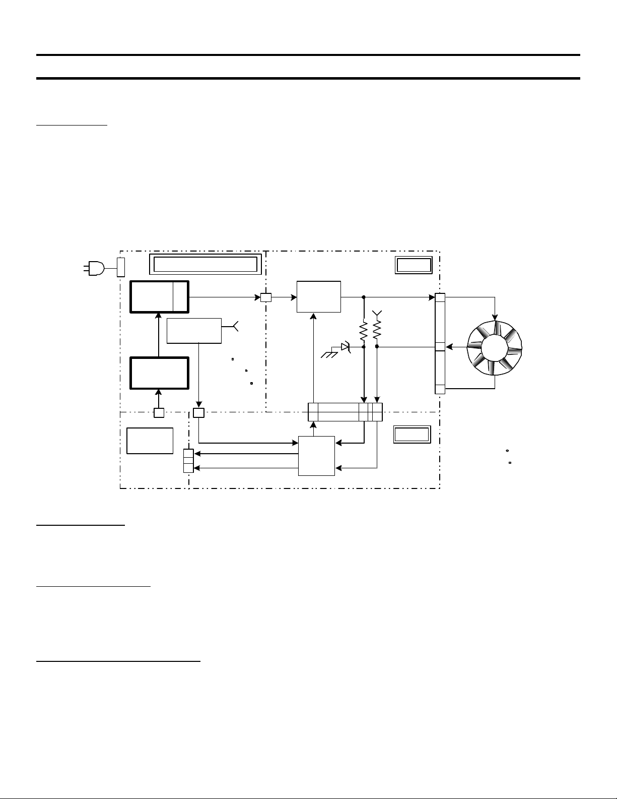
The fan is turned on when the TV is powered ON and blows air out of the TV. The TV will only shutdown when
the power supply (thermistor) reaches a critical temperature (set in the service mode), not if the fan stops.
Fan Operation
The fan runs at one of three speeds based upon the temperature of the power supply board. The power supply
board temperature is monitored by a thermistor that feeds IC6 (not shown). The output voltage of this thermistor
circuit at CN 1/pin 4 is a linear function of the temperature. 0 degrees C = 0Vdc. 100 degrees C = 4.7Vdc.
The Main CPU on the B board monitors the fan’s rotation and run voltage. This fan status is available as an OK
or NG indication in the user menu and service mode. In addition, the service mode displays the power supply
temperature. If the power supply temperature reaches critical (92 degrees for the 32" TV or 80 degrees for the
42" TV), the Main CPU discontinues the CPU_GO and RDP_GO signals and the TV shuts down. After shutdown,
the Standby light repeatedly blinks three times to indicate that high temperature was the cause of shutdown.
CN2
POWER SUPPLY BD.
IC11
PS3
IC21,IC22
CONTROL
CN7
PLASMA
PANEL
T2
*THERMO
6
CN1/
CN1203
5
6
CN3005
0V=0 C
0.8V=21 C
4.7V=100 C
4
CN1
THERMO
DRIVE
FAN
DRIVE
24
MAIN
CPU
18k
5V
FAN
FB
6 57
25 26
1
13V
5V
CN3003/
CN1001
CPU_GO
RDP_GO
FIGURE 11-1 - FAN DRIVE
Q BD.
CN3009
5V
ROTATION
= 0V
FAN
DET
B BD.
8.6V
1
0V
2
GND
3
FAN
* TV SHUTS
DOWN WHEN CN1/
PIN4
RISES TO:
4.3V-32" (92 C)
3.76V-42" (80 C)
2TVP13 1432 4/16/02
Fan Drive Voltage
When the TV is turned ON, the Main CPU (B board) outputs 5Vdc (CN1001/pin 24) to the fan drive block at
CN1001/pin 24. This allows the fan drive block (Q board) to output 12Vdc (connector CN3009/pin 1) to the run
the fan at start up. A run voltage from 8 to 12Vdc will always be present as long as the TV is ON.
Fan Rotation Detection
Within the fan, a Hall device detects rotation and grounds the voltage at CN3009/pin 2. This LOW is applied to
Main CPU and permits the temperature of the power supply board to adjust the Main CPU fan drive output
voltage. Typically at start up, the fan drive voltage at CN1001/pin 24 drops from 5Vdc down to 1.5Vdc to produce
8.6Vdc at CN3009/pin 1 to run the fan at slow speed.
Troubleshooting No Fan Rotation
If the fan is unplugged or there is no fan rotation detected, Main CPU reacts by turning ON the Fan drive signal
(CN1001/pin 24) to 5Vdc every two seconds (for a very short time; that may be difficult to detect except on a peak
reading DVM). This results in 12-volt fan run voltages that appear at the fan terminals (CN3009/pin 1) every two
seconds as long as the TV is ON.
30
Page 33
11. Fan Operation
Fan or Q board?
To determine if the fan, Q board or B board is causing NO fan rotation, turn ON the TV and:
1. Measure the voltage at the fan connector CN3009/pin 1 (red wire) with the fan connected (loaded).
2. Normal 12Vdc means the fan is bad. Replace the fan.
3. CN3009/pin 1= 0Vdc? You must inspect CN3005/pin 1 and CN1001/pin 24 at power ON.
• CN3005/pin 1 on the power supply board normally = 13Vdc
• CN1001/pin 24 on the B board normally = 5V pulse at power ON. The pulse can be read with a peak
DVM.
4. Is CN3005/pin 1, 0Vdc? Replace the power supply board.
5. Is CN1001/pin 24 at 0Vdc or stays at 5Vdc at power ON?
• 5Vdc at CN1001/pin 24 during power ON means the B board is OK so the Q board is bad.
• 0Vdc at CN1001/pin 24 during power ON means the B board is bad. Replace the B board.
Testing the fan
The fan should be tested by applying voltage to it.
Voltage Test:
The fan starts running when 6Vdc is applied (0.1A). You can also quickly start it using a 9V battery. Apply the
positive voltage to the red wire and negative to the blue wire.
Resistance Test:
A resistance check will only show you that a fan is not shorted. Resistance readings will not tell you if the fan will
run with voltage applied. Applying the ohmmeter positive leads produces these high resistances. Reversing the
leads permits you to read a diode in the Hall device.
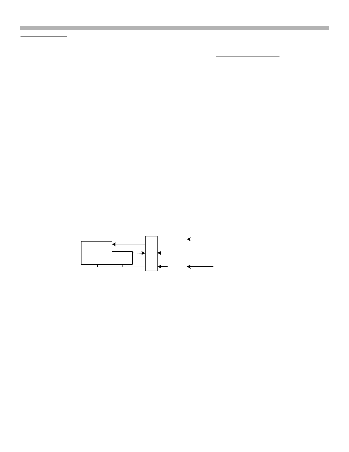
1
2
Infinity
3
Fan terminals =
1.7Meg ohms with
ohmmeter's 1.5v
battery
Fan
Circuit
red
Hall
blue
FIGURE 11-2 - FAN RESISTANCE TESTS
31
Page 34
12. Video Signal Flow
Chapter 12 - Video Signal Flow
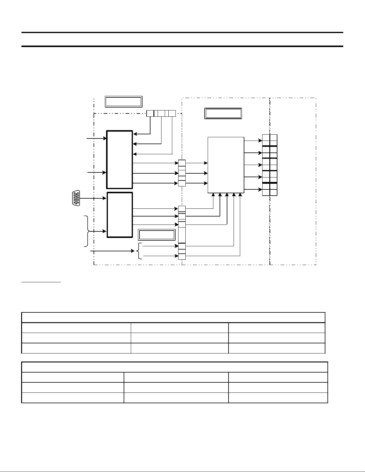
The video signal processing is performed on three boards (TU, Q and B) and the plasma panel as shown in
Figure 12-1. The composite video or component video is selected in the B board. The OSD is inserted into
the video path (not shown) later on in the B board signal chain. The output of the B board is digital video and
applied to the plasma panel. The video switching control for ICs on the TU, Q and B boards come from the
Main CPU, which is also on the B board.
S VIDEO
COMPOSITE
VIDEO
HD15
VGA
COMPONENT
VIDEO
Y,R-Y,B-Y
(Y,Cr,Cb)
SYNC
H+V
TU BOARD
TUNER VIDEO
L
R
IC3014
SW.
IC3001,
IC3011
SW.
CN102/
CN3004
1 3 5
L R
C
Y
VIDEO
CN3002/
CN401
R-Y
Y
B-Y
Q BOARD
H
V
CN3001
6
8
10
2
4
6
8
10
Cr
B BOARD
CHROMA
PROCESS
STATES
Y
Cb
CN1204/ CN1
H
V
323
547
7611
13
9815
17
111019
1
+
-
5
+
-
9
+
+
-
+
-
PLASMA
DISPLAY
PANEL
OUT 0
OUT 1
OUT 2
CLK OUT
OUT 3
Signal Levels
FIGURE 12-1 - VIDEO SIGNAL FLOW
3TVP13 1433 4/12/02
The tuner signal levels (Table 12-1) were taken with an NTSC generator set to channel 3. The S video levels
(Table 12-2) were taken using a DVD player. The component signal levels (Y, R-Y, B-Y in Table 12-3) were
also taken using a DVD player.
Table 12–1- Tuner Input
Signal Name Location Signal Level
Tuner Video (generator channel 3) CN3004/pin 1 1.2Vp-p
Video CN3001/pin 10 1.2Vp-p
Table 12–2 - S Video Input
S Video Signal Name Location Signal Level
Y CN3001/pin 8 1.2Vp-p
C CN3001/pin 6 0.6Vp-p
32
Page 35
12. Video Signal Flow
Table 12-3 - Component Video Input
Signal Name Location Signal Level
Y CN3002/pin 4 1.0p-p
R-Y CN3002/pin 2 0.8Vp-p
B-Y CN3002/pin 6 0.4p-p
Table 12-4 - Digital Video Signal Output to Plasma Panel
Signal Name From B Board To Plasma Panel Wire Color Signal Level *
Out 0 +/- CN1204/pin 2, 3. CN 1/pin 1, 3. Orange 0.7Vp-p
Out 1 +/- CN1204/pin 4, 5. CN 1/pin 5, 7. Yellow 0.7Vp-p
Out 2 +/- CN1204/pin 6, 7. CN 1/pin 9, 11. Pink 0.7Vp-p
CLK Out +/- CN1204/pin 8, 9. CN 1/pin 13, 15. Gray 0.7Vp-p
Out 3 +/- CN1204/pin 10, 11. CN 1/pin 17, 19. White 0.7Vp-p
* The main digital signal level is shown, but there are ten spikes of power supply noise in the body of
the waveshape that are not shown, bringing the signal level to 6Vp-p. The noise is also present on the
TV screen when the rear shield is not installed.
Waveshape *
Signal Name
Out 0 +/Out 1 +/Out 2 +/Out 3 +/-
+
-
10 usec/div. timebase
FIGURE 12-2 - DIGITAL VIDEO OUTPUT WAVESHAPES TO THE PLASMA PANEL
Location of Digital Input Connector CN 1 on the Plasma Panel
B Board
CN1204
Waveshape *
Signal Name
CLK Out
Approx. 30MHz
CN1 on the
plasma panel
FIGURE 12-3 - LOCATION OF DIGITAL VIDEO
SIGNAL CONNECTOR CN1
33
Page 36
12. Video Signal Flow
Digital Video Signal to Plasma Panel
Video signals Out 0 – 3 are digital video signals applied to the plasma video panel. Out 0 is the LSB (Least
Significant Bit) and Out 3 is the MSB (Most Significant Bit). The digital video signal is accompanied by a clock
signal for timing.
• Missing Clock signals (CLK Out) produce a dark screen (no picture) with normal sound.
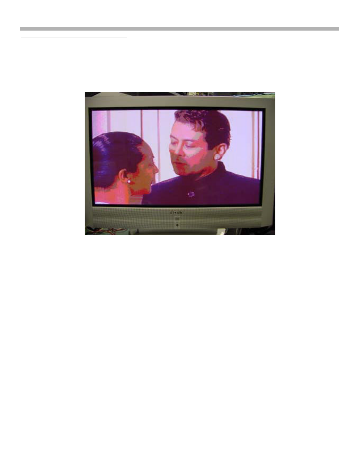
• Missing LSB signals Out 0 or Out 1 produce a picture without detail as shown in figure 12-4.
FIGURE 12-4 - TV Picture missing Out 0 or Out 1 LSB Picture Detail.
TV Picture missing “Out 0 or Out 1 LSB” picture detail. Splotches appear on faces or areas where there should
be detailed lines.
34
Page 37
13. What is Flat Screen Plasma Technology?
Chapter 13 -What is Flat Screen Plasma Technology?
The flat panel plasma display is the latest display technology and offers the following TV / monitor features:
• Bright screen light, easily viewable in any environment
• High resolution for excellent image quality
• Large, flat screen sizes
• Wide viewing angle
• Light weight
Flat screen plasma panels consist of cells that produce light. Three such cells of red, green and blue light form
a cluster known as a pixel. The brightness of the individual cell determines the color of the pixel. The number of
pixels on the screen is determined by the size of the screen. There are typically thousands of pixels on a screen
and there are three cells for each pixel.
Theory of Operation
Cell Operation
Each plasma cell functions much like a neon gas discharge tube or neon bulb. The bulb consists of two electrodes
in a tubular glass envelope filled with neon gas. When a voltage of approximately 65-70V (for a neon bulb) is
applied, the gas ionizes (resistance drops) and passes electricity. During ionization, an orange glow around the
negative (-) electrode is produced. Both electrodes appear to glow if AC is applied. Varying the current that is
allowed to flow (by changing the external series resistance) through the bulb controls the brightness.
Cell Structure
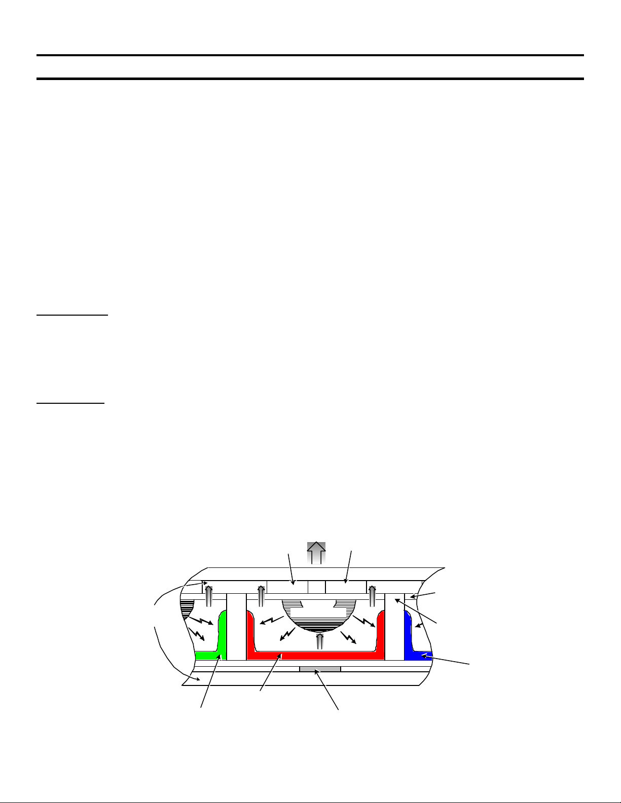
Refer to Figure 13-1 for the plasma cell structure. In a plasma cell, plasma replaces the neon gas in the tube.
Plasma is a collection of charged particles containing an equal number of + ions and electrons with properties
similar to gas, except they are conductive and affected by magnetic fields. When the Scan and Sustain electrode
(mounted on the glass faceplate) voltage reaches the electrical arc potential, the cell’s predominate neon and
xenon contents emit UV light. The UV light is converted to visible light by the red, green or blue phosphor of that
cell.
The data (also called index or address) electrode produces an induced electrical feedback signal to adjust cell
timing. The triad combination of one red, one green and one blue cell produces one pixel.
SUSTAIN ELECTRODE
(TRANSPARENT)
PROTECTION
BACK PLATE
LAYER
RIB
PHOSPHOR
(BLUE)
ELECTRIC
LAYER
PHOSPHOR (GREEN)
SCAN ELECTRODE
(TRANSPARENT)
FACE PLATE
DISCHARGE
PHOSPHOR (RED)
DATA ELECTRODE
FIGURE 13-1 - PLASMA CELL STRUCTURE
35
4TVP13 1435 4/15/02
Page 38
13. What is Flat Screen Plasma Technology?
Cell Intensity/Screen Brightness
The intensity of the cell is determined not by how bright it glows but by how often it fires within a field or frame.
The more times it fires, the brighter the cell seems (but actually they fire at full intensity each time). The number
of times it fires is based upon the phosphor persistence and is usually a maximum of eight times per frame.
1 2 3 4
9
5 6 7 8
16
FIGURE 13-2
SONY 16 X 9 PLASMA
PANEL SEGMENTS
Cell Selection and Screen Layout
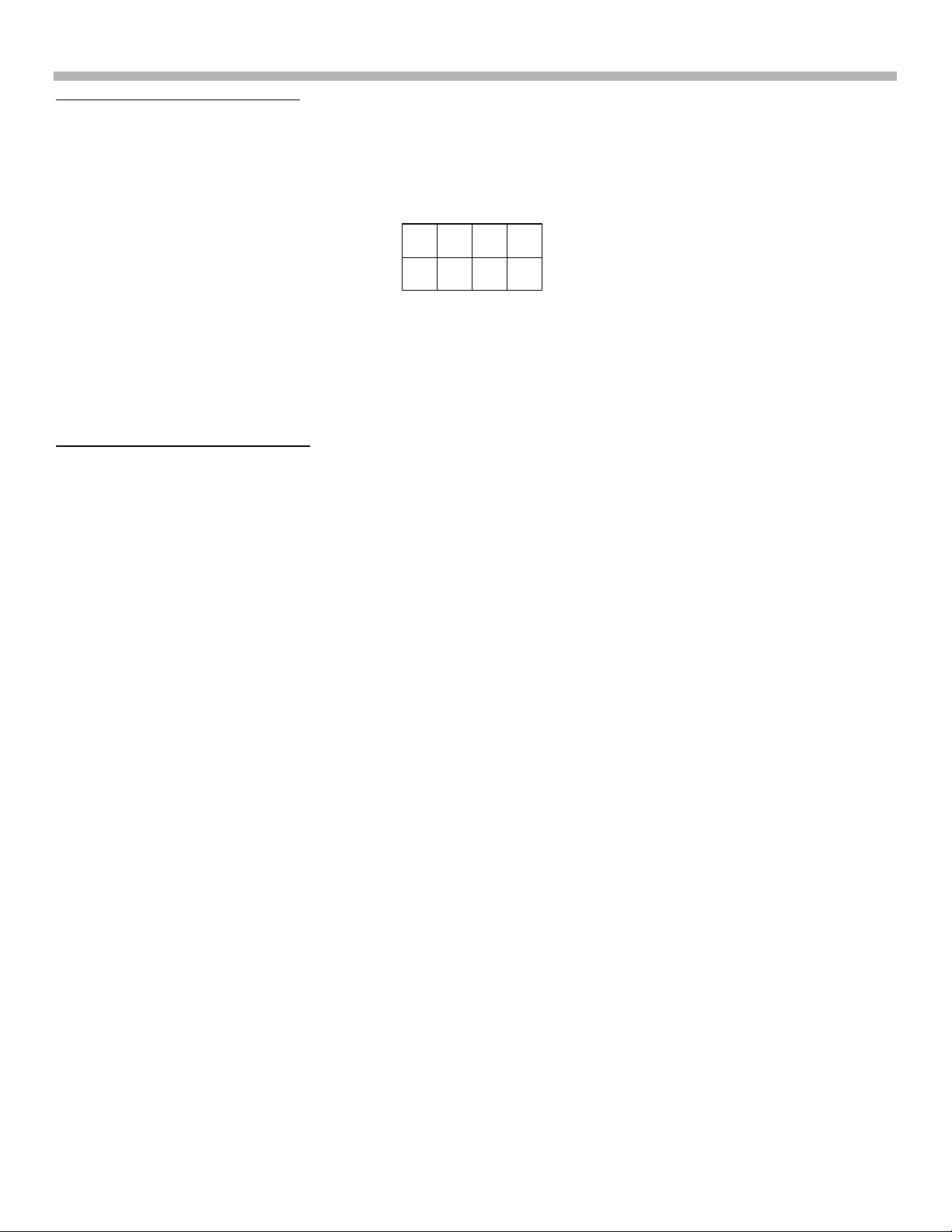
Within each panel, the individual cells to be fired are selected based upon the horizontal and vertical grid similar
to a multiplication table.
The screen is divided into eight panels as shown in Figure 13-2.
36
Page 39
Sony Model KZ-32TS1U // KZ-41TS1U TV Diagnostic Guide
Sony KF- 60DX100 Introduction
This portion of the training manual has been organized to enable you to quickly diagnose problems in the Grand
Wega 60" Projection TV model KF-60DX100. This Hi-Scan, 16x9 aspect ratio, LCD TV has a high brightness,
long life backlight that is user replaceable. Repairs involve determining which circuit board is defective, access
to the board and alignment afterwards.
This portion of the training manual is divided into 14 sections:
Table of Contents
Chapters Contents
15. Normal Operation This LCD Projector has a lamp and no convergence.
16. Self Diagnostics Look here for details when the Standby LED blinks.
17. Board Selection by Defect Listing of possible defects and related boards by probability.
18. Board Location Picture of the boards in the TV.
19. Adjustments Video adjustments when changing the BB, BC or M board. No
convergence adjustments.
20. Service Mode Access and new contents.
21. Determining if the Optical Unit is
OK.
22. Optical Unit Removal Pictured steps.
23. Screen / Mirror Replacement The entire top of the TV is replaced as an assembly.
24. Troubleshooting – TV Shutdown Dead set and Shutdown flow charts.
25. Power ON Circuit Description Standby circuit description and power ON sequence.
26. Fan Control Description Fan Drive Signal, Rotation Detection and Troubleshooting
27. Lamp Control Circuit Description Operation, Operation Time, Removal and Troubleshooting.
28. Video Process Block Diagram of the Video flow showing CCD & OSD entry
Symptoms are: Shutdown, white or black screen or missing color.
points. Troubleshooting charts and tables for shutdown, dark
screen, white screen or video distortion.
37
Page 40
Sony Model KZ-32TS1U // KZ-41TS1U TV Diagnostic Guide
Chapter 15 - Normal Operation
Satellite reception shows picture squares – The compression of satellite conveyed (“Dish”) video signals
results in pictures that show small squares larger than the detail the TV is capable of producing. This problem is
compounded by the DRC circuit, which cannot enhance the picture detail by analyzing the picture’s larger squares
and making improvements.
When high compression is used, the DRC circuit cannot properly analyze the picture. To ensure that the DRC
circuit does not add more noise; the TV menu has a MILD picture mode (i.e. VIVID, STANDARD, MOVIE &
MILD) that bypasses the DRC operation. The MILD mode can be used on any noisy program.
Lamp Life – Estimated lamp life is about 6000 hours, P/N = XL2000U (A-1601-753-A). The lamp life will be
shortened if the lamp is repeatedly started or run at elevated temperatures.
Lamp Warm Up – The backlight lamp is similar to a fluorescent tube but has a two level brightness and delay
circuit to prolong life. At turn ON, the lamp gradually increases to the first level of low very brightness. Three
seconds later, a lamp relay (on the lamp board) will click to move to toward the second brightness level. After the
lamp relay clicks, the lamp will take a minute to gradually reach almost full brightness.
Lamp Remains ON – Although the audio and video is muted immediately at turn OFF, the TV remains on for five
seconds afterwards. During these five seconds, the lamp steps to a lower brightness while the fans continue to
cool. The lamp that remains ON when the TV is muted is only noticeable if the room is dark.
Delayed TV ON - If the TV is turned OFF and back ON within five seconds before the lamp goes off, the TV will
come back ON (unmute). However, if the TV is turned ON after the lamp has turned OFF, the TV remains audio
and video muted for 30 seconds. This allows time for the lamp to cool off before being turned back on. Turning
a lamp on and off quickly shortens its life.
No Convergence Adjustments – The positioning of the three colored LCD panels is performed at the factory.
Since there are not three beams to converge, convergence is a matter of positioning the three LCD panels with
minor adjustments at the factory. If there are geometric distortions, check the cabinet for shifted mirror, front lens
and cabinet deformation (weights added to the cabinet) before suspecting the optical unit assembly that contain
the LCD panels.
38
Page 41
Sony Model KZ-32TS1U // KZ-41TS1U TV Diagnostic Guide
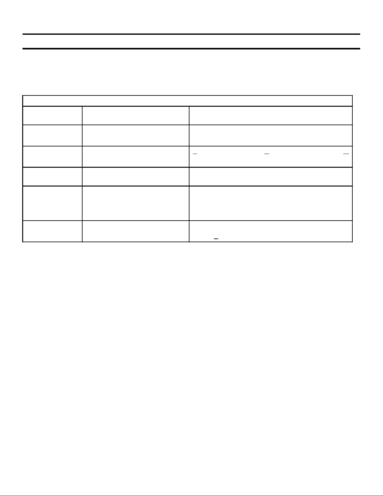
Chapter 16 - Self-Diagnostics
The front panel Lamp LED flashes continuously when the lamp reaches end of life and fails to ignite.
The front panel Standby LED blinks to indicate a more serious fault. If the TV starts and shuts down, the LED will
repeatedly blink a number of times to indicate the reason for shutdown. The boards that can cause TV shutdown
are listed in Table 16-1.
Table 16-1 - Self-Diagnosis
Standby LED
blinks
3 times Lamp cover door is not closed.
(See Lamp Control diagram)
4 times Fan rotation is not detected.
(See Fan Control diagram)
5 times Power Block board cannot turn
on the lamp.
6 times Low or missing 5Vdc. G board or a load on the 5V line (any board). If the
9 times L/R Audio Output speaker line
monitored for 0Vdc.
This self-diagnostic information is also stored in memory and viewable on the TV screen. It is accessed by
aiming the remote at the TV and pressing the following buttons: Display, 5, Vol -, Power. Half of the list above
will be shown on the TV screen. Moving the joystick left or right permits you to see the remaining self-diagnostic
categories. The number of times the failure has occurred is displayed to the right of the intermittent problem.
Clearing this memory requires you to exit this program by shutting off the TV, entering the regular service mode
(Display, 5, vol +, Power), and pressing 8, Enter.
Cause Suspected board
Lamp cover switch not shorted (T board).
A board (fan control), G Bd (Power supply) or M
Bd. (control).
Power Block board or the Lamp.
problem is not on the G board, unplug each board,
then power ON the TV to see if 5Vdc appears at
CN1604/pin 1. Remove the BB board first.
G board (power supply) or A board (audio output).
Check +15Vdc fuses PS1601, & 1602 on G board.
39
Page 42
Sony Model KZ-32TS1U // KZ-41TS1U TV Diagnostic Guide
Chapter 17 - Board Selection by Defect
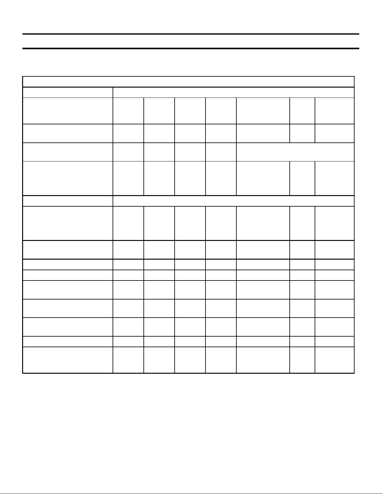
This table shows the boards that could cause the symptoms listed. The most likely board is designated #1, the
second likely #2, etc.
Table 17-1 Symptoms and Related Circuit Board
Probable board failure
Symptom A BB
(Video)
Audio Problem 1 2 – ck fuses
Dark Screen sound OK 3 2 1 4 *See “Determining if the optical unit
Dead Set – no relays heard 1 also ck for
Dead Set – relays click See Standby indicator blinks
Stby LED blinks 3 times 1 – Ck
Stby LED blinks 4 times 1-Fan,
2-A Bd.
Stby LED blinks 5 times 1 2
Stby LED blinks 6 times 3 2 5 4 1 6
3
BC
(Video) C (optical
unit)
G (PS) Lamp
Driver
PS1601-2
is OK” for quick tests.
open BiMetal
fuse under rear
fan.
M (Micro)
lamp
cover Sw;
2- M Bd.
Stby LED blinks 9 times 2 1 – ck fuses
PS1601-2
Video Distortion – Tuner &
composite Video
Video Distortion –
component video
Video Distortion – all inputs 1 2
Symptom A BB BC C
2 1
1
G Lamp
(optical
unit)
Driver
M
40
Page 43
Sony Model KZ-32TS1U // KZ-41TS1U TV Diagnostic Guide
Chapter 18 - Board Locations
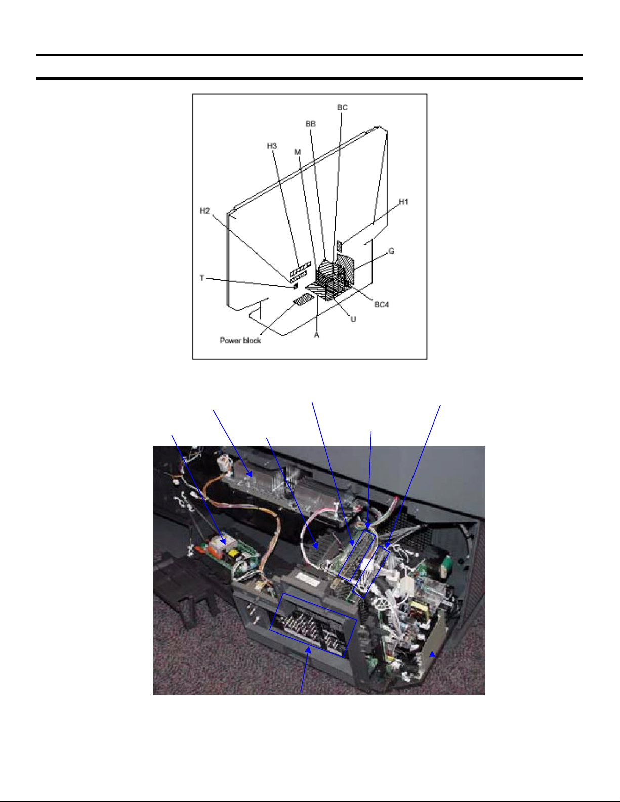
Power Block
(Lamp Power
Supply)
FIGURE 18-1 - BOARD LOCATIONS
Optical
Unit
Bottom
A Board
BB Board
BC BoardM Board
U Board
FIGURE 18-2 -BOARD LOCATION
41
G Board
(Power Supply)
Page 44
19. Adjustments
Chapter 19 - Adjustments
White Balance / Brightness
The service manual shows a series of white balance and brightness level adjustments for the TV, Twin, Video
inputs and component inputs. They can be touched up when changing the BB and BC boards and must be
adjusted when replacing the M board.
Geometric Distortion
There are no adjustments for geometric distortion. That is adjusted in the preassembled optical unit. If there is
geometric distortion, inspect the mirror (top) area of the TV for damage.
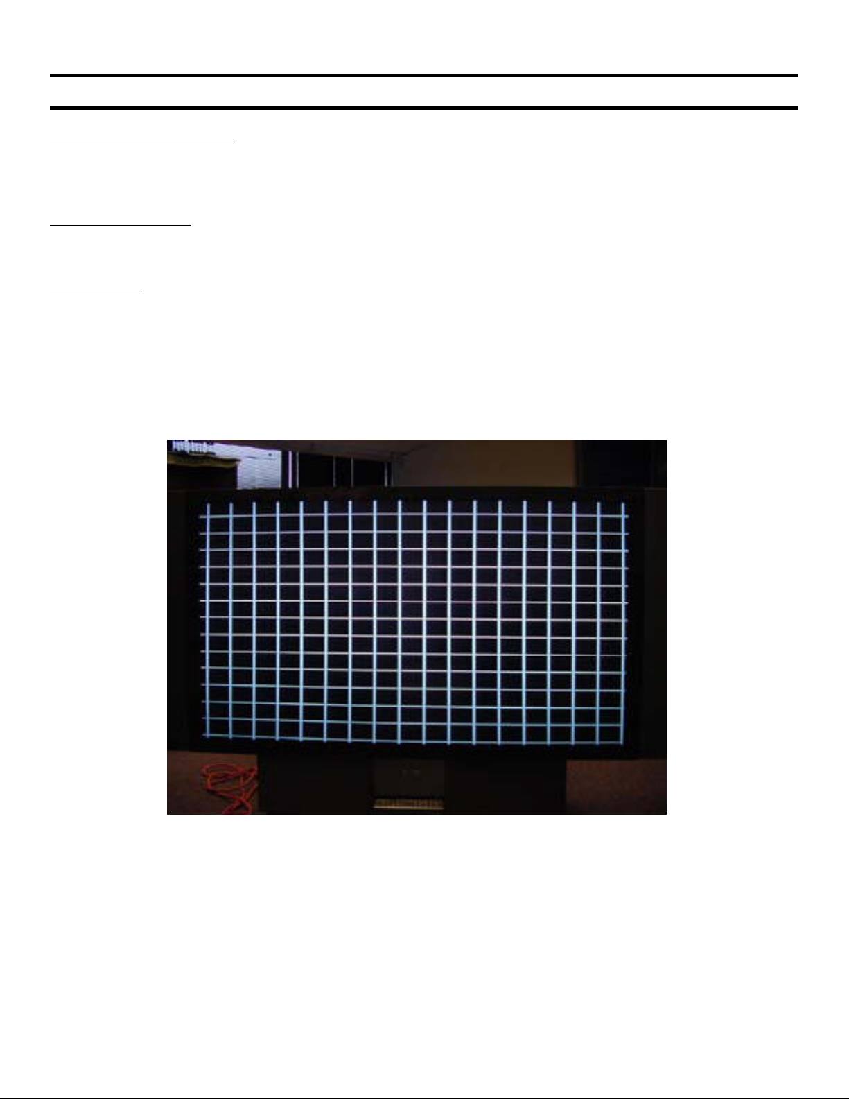
Convergence
Convergence is not adjusted in this set. The LCD panels are positioned at the factory for convergence. Figure
19-1 shows a crosshatch pattern. If convergence is off, the top mirror assembly and the optical unit where the
LCD panels are located are both suspect. If the misconvergence is on one side of the screen accompanied by
geometric distortion, the mirror may have broken from their mounts. In this case, reinstall the mirror or replace
the entire upper assembly (mirror, screen, bezel and speakers as one assembly. P/N = A-1603-167-A.
Figure 19-1 - Typical Crosshatch using an External Generator
42
Page 45
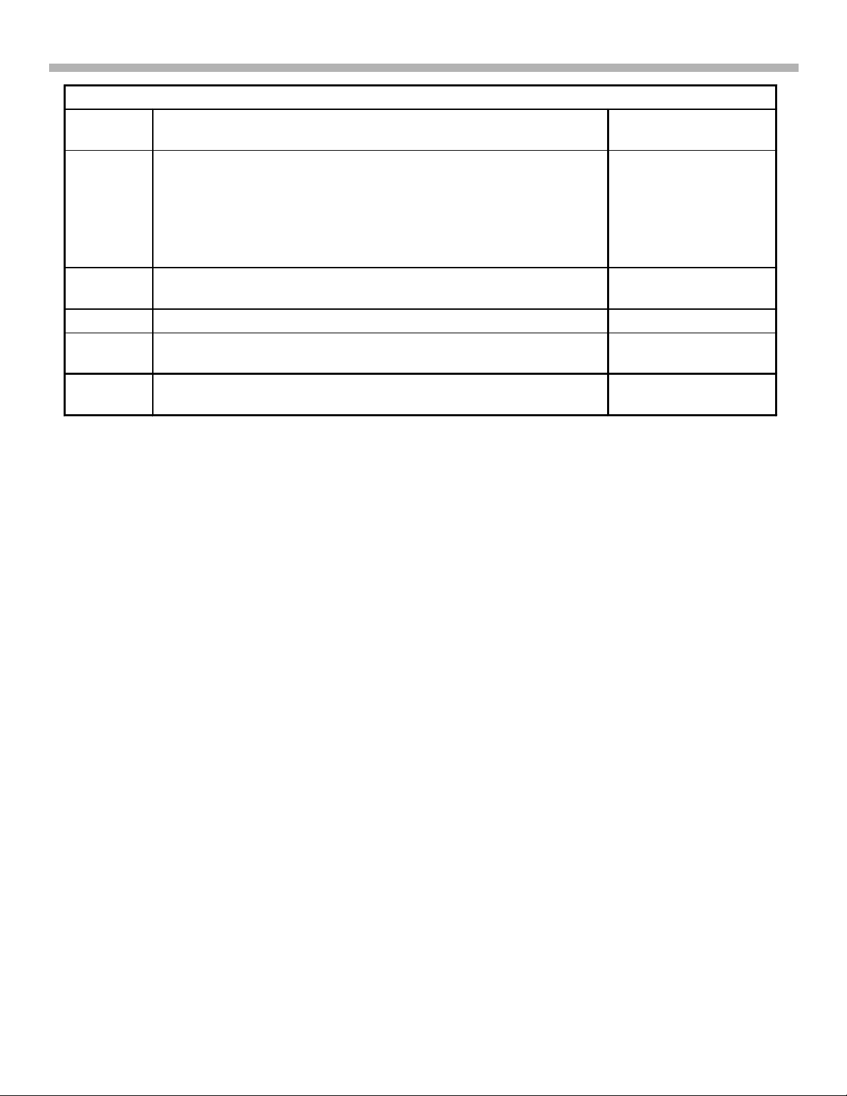
Table 19-1 - Adjustments after Board Replacement
19. Adjustments
Board
Replaced
Light Box
(Optical
Unit)
A board Picture Adjustments (RF, video and component inputs are
BB board Same as above. Section 3-2, page 39
BC board Same as above except component video levels need not be
M board Same as for the A or BB boards unless the NVM IC9002 is
1. Screen Center Adjustment to center the picture.
2. Vertical Stripe Adjustments – There are alternate even and
odd rows of dots across the screen (L-R). Adj. the even dots
to the same brightness as the odd dots. First adj. red dots
with a Red field, then Green and finally Blue. You must be at
the screen to see the even vs. odd dots.
adjusted for consistent white level and color).
adjusted.
transplanted to the new M board.
Adjustment Service Manual page
Section 3-5, page 43
Section 3-3, page 42
Section 3-2, page 39
Section 3-2, page 39
Section 3-2, page 39
43
Page 46
5. Adjustments
Chapter 20 - Service Mode
Access: Conventional – From the remote press Display, 5, Vol +, Power ON. Category selection = buttons 2 (up)
and 5 (down). Item selection = buttons 1 & 4. Data change = 3 & 6. Store data = Mute, Enter.
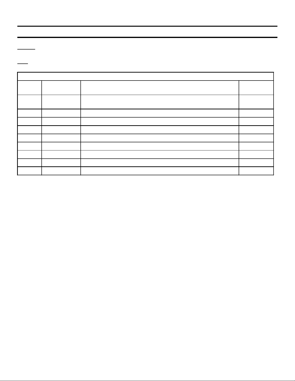
New: The details of New Category “Option E” for lamp information and fan control are clarified and is shown in
Table 20-1
Table 20-1 - Contents of Service Mode Option E
Item
number
0 Lamp Time Lamp operating time in hours. Hours shown when data is
1 Lamp Off Lamp time after TV turns OFF. 0=0sec. 1=5 seconds. 1
2 Fan Off Fan time after TV turns OFF. 0 = 0 mins. 1 = 2 mins. 0
3 Fan 1 RPM 1 LCD Fan speed - TV ON. 3 speeds. 0 = slow 2
4 Fan 1 RPM 2 LCD Fan speed after TV is OFF. 3 speeds 2
5 Fan 2 RPM 1 Lamp Fan speed – TV ON. 3 speeds. 0 = slow 1
6 Fan 2 RPM 2 Lamp Fan speed – TV OFF. 3 speeds 1
11 P CTL Sht 1 LCD video position. Correction 1 after hours 10
12 P CTL Sht 2 LCD video position. Correction 2 after hours 60
Name Description Typical Data
0
changed to 1. Reset when data 0 is stored (mute, enter).
44
Page 47
5. Adjustments
Chapter 21 - Determining if the Optical Unit is OK
The optical unit can fail, producing:
• TV Shut down by loading down the power supply.
• White or black screen.
• Missing a color.
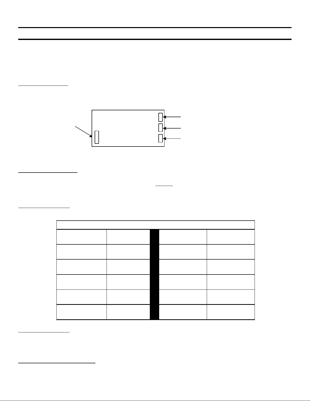
If the TV shuts down (probably without a Standby LED fault indication), the optical unit can be unplugged and the
TV powered up to see if the TV remains ON. Normally, when all four cables to the optical unit are removed, the
TV will display a no picture bright white screen with sound (OK). If only the RGB signal input cable at CN5005
were unplugged, the screen would be ¼ bright, sound OK.
CN5002
Power In
Orange
CN5005 RGB, sync in (gray)
CN5001 DATA, blanking (red)
CN5004 S Data (white)
FIGURE 21-1 - OPTICAL UNIT CONNECTORS (TOP VIEW)
White or Dark Screen - In a conventional TV, a loss of signal results in a white screen. This is also true in this
LCD projection TV. However, if the screen is dark with normal sound, the LCD optical unit or the previous circuit
board may be bad. On the other hand, a dark screen without sound indicates video and audio muting by the
Main Micro. This is because of either: a communications problem with another IC, a fan defect, a lamp circuit
defect, or an audio output failure which may also cause TV shutdown but not a video failure.
If the screen is white, there may be no input to the optical unit. Check for loss of input voltage at CN5002 and
RGB input signal at CN5005. If the input voltages and signals are present, the optical unit is suspect.
Table 21-1 - Optical Unit Input Voltages and Signal Levels (color bar input)
Input Voltage
(from G board)
CN5002/pin 1
(white)
Level Input Signal
(from BB board)
- 7Vdc CN5005/pin 1
(Blue signal)
Level
2.5Vp-p
CN5002/pin 3,4
(orange)
CN5002/pin 7,8
(orange)
CN5002/pin 11
(orange)
CN5005/pin 9
5Vdc CN5005/pin 3
(Green signal)
3.3Vdc CN5005/pin 5
(Red signal)
15Vdc CN5005/pin 7
(Vert sync)
(Horiz sync)
2.0Vp-p
2.4Vp-p
5Vp-p
5Vp-p
If the screen is black, the optical unit or BB board may be bad.
Determine which one by unplugging the CN5002 power connector to the optical unit. If the screen becomes
white, the BB board is bad. A white screen is normal if the optical unit loses power (it passes all the backlight).
If the screen remains black, the optical unit is bad.
If the screen is missing a color, the RGB signals entering the optical unit (CN5005) have to be verified before
accusing the optical unit of the failure. The signal levels are given in Table 21-1.
45
Page 48
22. Optical Unit Removal
Chapter 22 - Optical Unit Removal
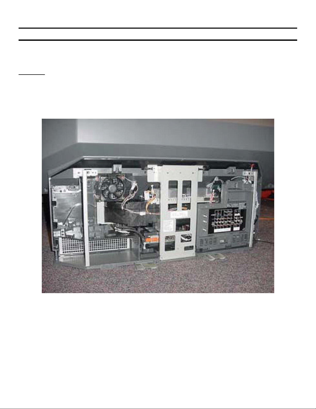
The optical unit contains the video output portion of the TV in one assembly with three colored LCD panels and
the C board. The optical unit is held in with just two screws, but the TV board assembly and the power block
board must be pulled out to access these screws. The optical unit is replaced as an assembly.
Procedure
a) Remove the lower back panel and the three support brackets (Figure 22-1)
FIGURE 22-1 - THREE SUPPORT BRACKETS
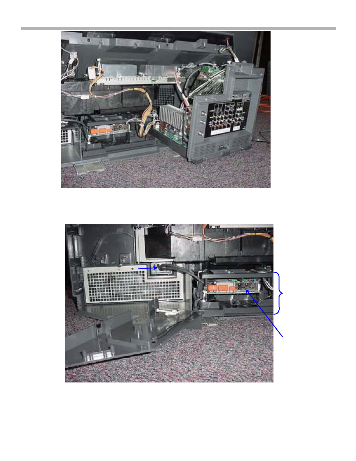
b) Lift the TV board assembly up and outward (Figure 22 -2)
46
Page 49
22. Optical Unit Removal
FIGURE 22-2 - TV BOARD ASSEMBLY SLIDES OUTWARDS
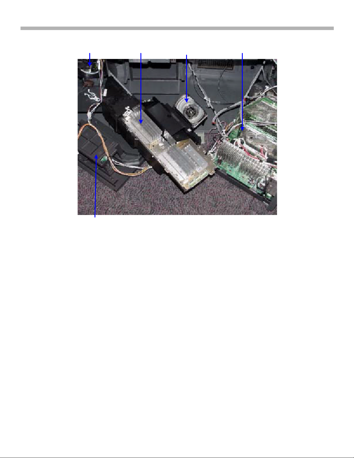
c) Remove the two screws holding the lamp socket (Figure 22-3). The power block HV wires are not long
enough to permit the power block to swing out of the way.
HV Lamp Socket
Power Block
Assembly
Power Block
(Lamp Driver
Board)
FIGURE 22-3 - REMOVE TWO HV LAMPSOCKET SCREWS
d) Lift the Lamp board assembly up and outward (figure 22-4)
47
Page 50
22. Optical Unit Removal
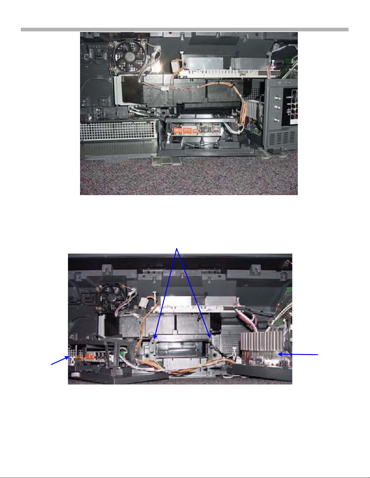
FIGURE 22-4 - POWER BLOCK UP AND OUT
e) Loosen the two screws under the optical unit (Figure 22-5). The screws are part of the optical unit.
Optical Unit
Assembly
Screen
Power
Block
Board
Assembly
TV
FIGURE 22-5 - OPTICAL UNIT SCREWS EXPOSED
f) Slide out the optical unit.
48
Page 51
Lamp
Optical
Unit
Assembly
Lens
22. Optical Unit Removal
TV Board
Assembly
Power Block
Assembly
FIGURE 22-6 - OPTICAL UNIT ASSEMBLY
g) Dust the optical unit lens with a soft cloth before installing. Specks of dirt are magnified, so clean it carefully.
49
Page 52
23. Screen / Mirror Replacement
Bracket
Chapter 23 - Screen / Mirror Replacement
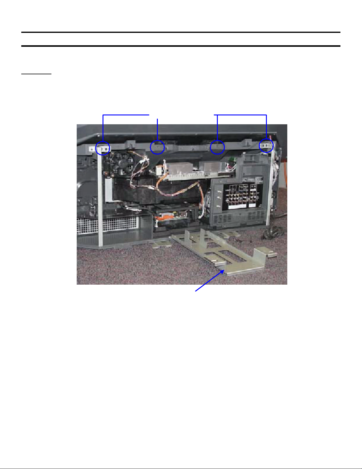
The entire top of the projection TV is replaced as an assembly containing the screen, mirror and speakers.
Procedure
a. Remove the back (lower) panel.
b. From the back, remove the center support bracket.
4 Top Assembly Screws
Center Support
FIGURE 23-1 - REMOVE THE REAR CENTER SUPPORT BRACKET AND SCREWS
c. Also from the back, remove the four screws securing the top assembly to the lower electronics (Figure 23-1).
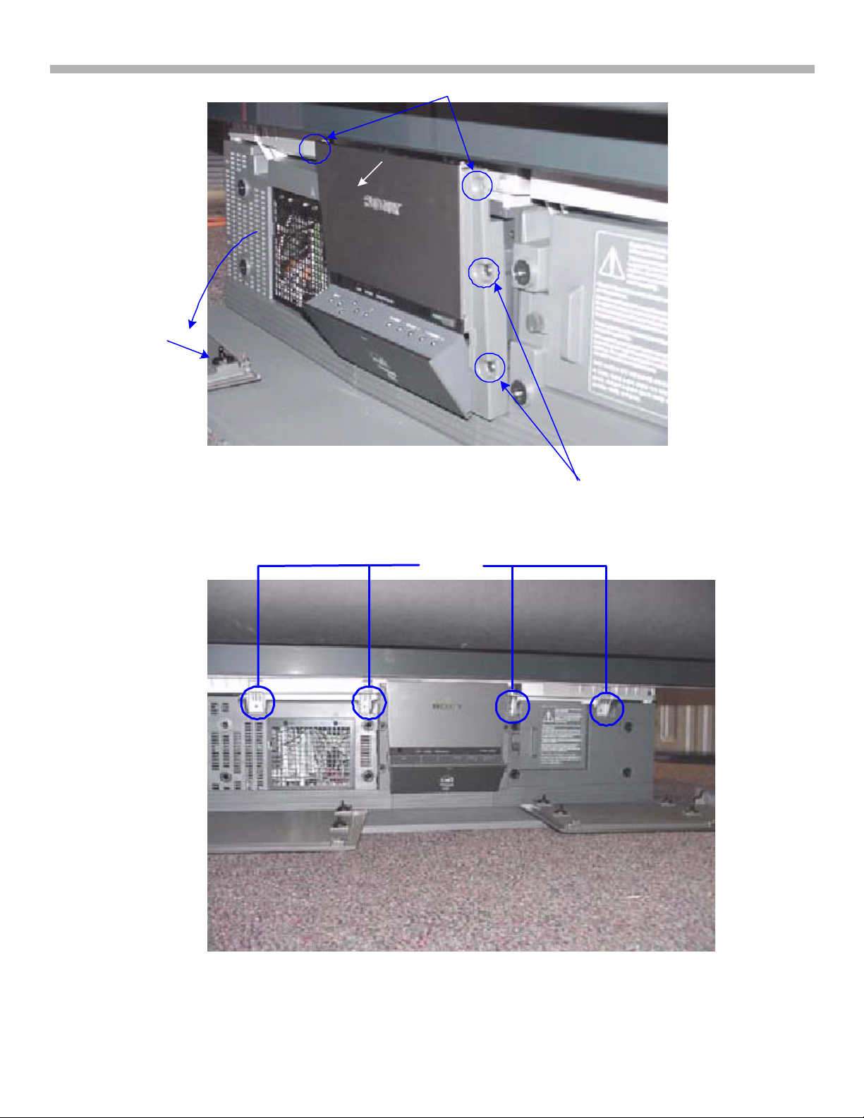
d. Refer to Figure 23-2. From the front of the TV, pull the two side panels off to expose the control panel screws.
e. Remove the top two screws of the control panel and loosen the remaining four by ½ inch. Tilt the control
panel forward as shown in Figure 23-2.
50
Page 53
Pull off
L & R
Panels
23. Screen / Mirror Replacement
Remove Screws
Tilt Out
1/2"
FIGURE 23-2 - PULL OFF THE FRONT SIDE PANELS & LOOSEN CONTROL PANEL
f. From the front, remove the remaining four screws (Figure 23-3).
4 Screws
Loosen
FIGURE 23-3 - REMOVE THE TOP FOUR SCREWS
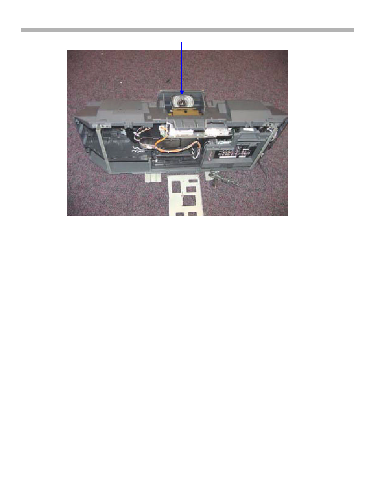
g. With the help of another person, lift the top assembly off. Do not leave the glass mirror in the top assembly
exposed to dust and children. Clean the lens with a soft cloth (Figure 23-4) before installing the top assembly.
51
Page 54
Lens
23. Screen / Mirror Replacement
FIGURE 23-4 - BOTTOM TV BASE
52
Page 55
9. Screen / Mirror Replacement
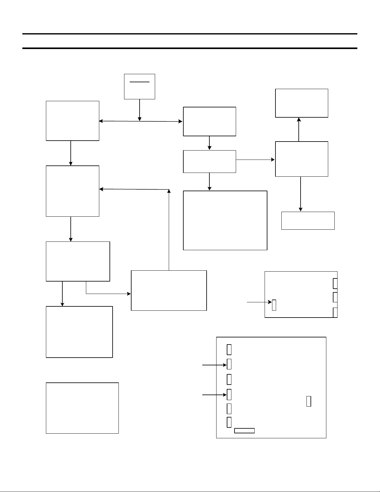
Chapter 24 - Troubleshooting - TV Shutdown
The TV can be disabled because of: open bimetal fuse, fan not working, lamp not working, short on the 5Vdc line
and an imbalance in either audio output stage.
START
POWER
TV Dead - No
Relay click at
power ON attempt
ON
Relays Click, then
TV shuts down
Replace M
board
No
On the power
supply bd. Short
CN1614. If TV
comes ON,
replace bimetal
fuse under fan.
Problem with G, M or
A boards. Measure
CN1605/pins 4 and 5
at power ON.
Defect:
CN1605/pin 4 = 0Vdc G board defective.
Standby LED
indicator blinking?
Stby LED blinks:
3 times - Lamp cover sw.
4 times - Fan, A, G, M board
5 times - Lamp board
6 times - G board
9 times - G or A board
Normal:
CN1605/pin 4 = 7Vdc
CN1605/pin 5 = 5Vdc
G board bad or Sw bad.
Yes
CN5002
No
Unplug optical unit
power CN 5002.
TV powers w/
white screen?
Yes
Replace optical
unit
Optical Unit
Top View
CN1605/pin 5 = 0Vdc M or A board is bad.
Measure CN1921/pin 21
at power ON.
CN1921 is under the TV
board assembly.
0vdc - M board bad
5Vdc - A board bad
FIGURE 24-1 - TV DEAD / SHUTS DOWN FLOWCHART
CN1614
CN1605
53
Power Supply
G Board
Gnds
Page 56
25. Power Supply
Chapter 25 - Power Supply
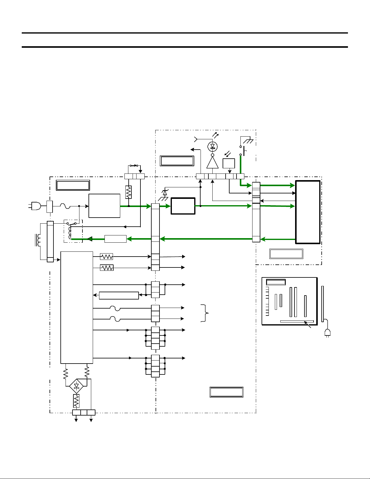
The Standby power supply circuit and power ON sequence is simple and easy to figure out by looking at the
simplified Figure 11-1. The only outstanding servicing precaution you must make note of is the over voltage
zener diode on the A board at CN1901/pin 3 in Figure 25-1. If it shorts, it will load down the standby 5Vdc and the
TV will not respond to a power ON command (dead TV set).
Standby Power Supply
The standby power supply is located on the G board with the main power supply. Standby voltage is output when
the TV is plugged into AC. Standby 7Vdc is output CN1605/pin 4 into the bottom A board where it is regulated
down to 5Vdc and passed onto the Main Micro on the M board (via CN1921/pin 16).
0.2Ω
1
3
CN1616
R1654
BI-METAL FUSE
LOCATED
UNDER REAR
CN 1614
G BD.
F1601 6.3A
STANDBY
POWER
SUPPLY
PWR RELAY RY1601
ERROR REG.
MAIN
POWER
SUPPLY
PS1602
R1655
SMP-B28
FAN
R1627
22 1W
Q1603
R1618
R1617
PS1601
11V
4.5V
3 1
STBY
7V
5V=ON
0V=OFF
0.5Ω
7V
STBY
5V
H3 BD.
D1931
4
IC1905
REG.
CN1605/
CN1914
5
2
1
17V
33V
CN1604/ CN1926
1
2
CN1606/ CN1909
2
6
1
2
3
4
1
2
3
4
CN1613/
CN1914
CN1603/
+15V
-15V
CN1915
3 7 5
POWER
CONTROL
5V
11V
4.5V
STBY
LED
IR
STBY 5V
AUDIO
POWER
CN4502/
CN1901
4
CN1921/
CN9001
POWER
48
SIRCS
47
STBY LED
45
16
STBY 5V
21
A BD.
TUNERS
BOARD LAYOUT
PWR
ON
M BD.
M BB
IC9004
MAIN
MICRO
G
BC
U
R1613
+
1 3
270V TO LAMP
DRIVER BD.
A BD.
CN1602
-
FIGURE 25-1 - POWER ON BLOCK - KF-60DX100
54
5TVP13 1438 4/11/02
Page 57
25. Power Supply
BOTTOM VIEW OF A BOARD
Power ON sequence
After the Main Micro IC9004 (M board) receives standby power (CN1921/pin 16), IC9004 can respond to the
power ON command from either the remote (IR) or the switch on the front panel H3 board. The TV power ON
steps are:
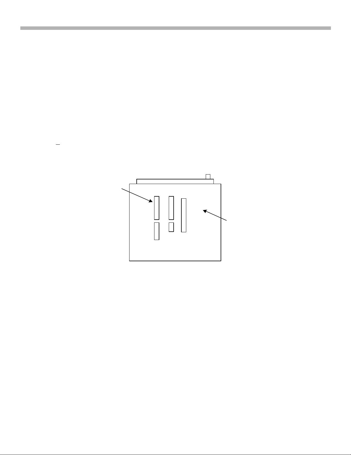
1. The front panel power ON button is pressed. CN1921/pin 48 goes LOW (0Vdc – see Figure 25-2 for the
location of CN1921/CN9001).
2. Main Micro IC9004 outputs a HIGH (5Vdc) to energize the power relay. CN1921/pin 21 goes to 5Vdc.
3. This 5Vdc passes through the A board into the power supply (G) board at CN1605/pin 5 = 5Vdc.
4. If the Bi-metal fuse under the lamp fan 2 is closed (CN1614/pin 1 & 3 connected), then the power ON
command into CN1605/pin 5 = 5Vdc can energize the power relay RY1601 on the A board.
5. Within the G board, power relay RY1601 contacts close, passing AC to the Main power supply. The Main
power supply outputs various voltages to power the TV.
6. Only the +15 voltages (CN1606/pin 2, 6) that go to the audio output stage are fused. Fusible resistors are in
the 33Vdc and 17Vdc outputs at CN1605/pin 1, 2.
Rear Panel VHF
CN9001
1
M BB BC
Board
Connectors
Bottom
A Board
FIGURE 25-2 - TV BOARD ASSEMBLY
55
Page 58
26. Fan Control - KF-60DX100
Chapter 26 - Fan Control - KF-60DX100
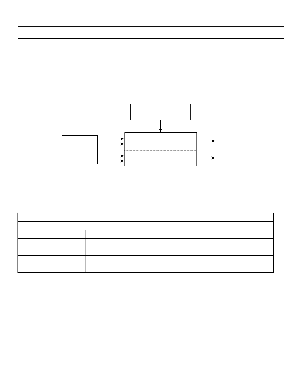
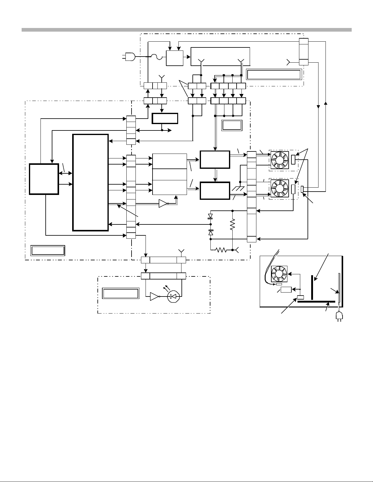
This Sony Grand Wega LCD Projection TV has two fans that start when the TV is turned ON and stop five
seconds after the TV is turned OFF. Fan 2 is located at the rear and is visible as soon as the rear panel is
removed. It cools the lamp block/assembly underneath it. Fan 1 is hidden under the LCD Optical assembly /
light box.
Both fans contain Hall effect devices and circuitry that monitor fan rotation. If the Main Micro (M board) detects
no rotation from either fan, the TV shuts down within five seconds.
In addition to this protection, if the temperature of the lamp assembly reaches a critical level, the TV will also turn
OFF. A replaceable Bi-Metal fuse located under fan 2 (lamp cooling) will open if the lamp assembly gets excessively
hot.
Power Supply G Board
11Vdc
Sw
Main
Micro
Regulator IC1908
5V
LCD Fan 1
M Board
Regulator IC1909
A Board
FIGURE 26-1 - FAN CONTROL BLOCK
9V
Lamp Fan 2
4/16/02
Fan Drive
Refer to Figure 26-1. The power supply board’s 11Vdc (CN1613/pin 1-4) source powers both fans. In-between
the power supply and fan is the A board. On the A board is regulator IC1908 that provides switched 5Vdc to the
LCD fan 1 and IC1909 to provide switched 9Vdc to the Lamp fan 2.
Table 26 -1 Fan Control
LCD Fan 1 = ON Lamp Fan 2 = ON
A Board Connector Voltage A Board Connector Voltage
CN1920/pin 20 0Vdc CN1920/pin 18 0Vdc
CN1920/pin 21 0Vdc CN1920/pin 19 5Vdc
CN1920/pin 22 5Vdc CN1920/pin 22 5Vdc
CN1914/pin 1, 2, 3, or 4. 11Vdc (supply) CN1914/pin 1, 2, 3, or 4. 11Vdc (supply)
Five voltages from CN1920 are input the A Board, along with the supply voltage at CN1914 (11Vdc). When these
voltages are input, the A Board will output 5V and 9V to power their respective fans.
56
Page 59
26. Fan Control - KF-60DX100
CN1614
1
DATA
IC9004
MAIN
MICRO
S
CLK
LAMP
LED
M BD.
HALL DEVICES
*
DETECT FAN
ROTATION
S
CN1605/ CN1914
IC9502
FAN/
LAMP
CONTROL
CN9001/
CN1921
CN9501/
CN1920
H3 BD.
21
16
26
20
21
18
19
22
23
45
7V
5 4
4
5
IC1905
0V
H
FAN 1
L
0V
CONTROL
0V
H
FAN 2
L
5V
5V=ON
0V=OFF
5V=SHUTDOWN
0V
0V=NORMAL
STBY
0V
7
7
Q4508
STANDBY LED
RY
1601
CN1604/
CN1926
7V
STBY
5V
Q1905
5V
3
3
POWER
5V 11V
SUPPLY
12 2 3
112
1 2 3 4
11V
5V
IC1908
REG
1.2V
IC1909
REG
FAN 2 PWR 9V
D1901
D1902
CN1901
CN5402
A BD.
FAN 1
PWR 5V
0V
0V
7V
PWR SUPPLY BD.
4
CN1613/
CN1914
FAN 1
RED
6
5V
5
BLK
BLU
7
9V
9
RED
FAN 2
8
YEL
10
CN1908
5V
FAN 1
CN1908
FAN/BOARD LOCATION
*
DEVICES
WHITE
BI-METAL
FAN 2
TV REAR
3
HALL
BI-METAL
FUSE
UNDER
FAN 2
0V
M BD.
PS
BD.
A BD.
FIGURE 26-2 - FAN CONTROL - KF-60DX100
7TVP13 1442 4/16/02
Fan Rotation Detection
When drive voltage to the fan is present, the fan rotation detector output will ground out the 5Vdc input at
CN1908/pins 8 & 10. This ground (0Vdc) keeps the Main Micro from turning OFF the TV.
If either fan stops rotating, CN1908/pins 8 or 10 will rise to 5Vdc. This 5Vdc is detected by Min Micro IC9004
(CN9020/pin 45 *) and IC9004 shuts off the TV in five seconds.
* CN9020 can be accessed from under the A board. Tilt the TV board assembly up and locate the marked pin.
57
Page 60

26. Fan Control - KF-60DX100
Troubleshooting
If the backlight does not start and the TV shuts down with the Standby LED blinking four times, one or both of the
two fans has stopped. The suspected boards are: A board (fan regulators), G board (power supply) and M board
(fan control).
Procedure
1. At power ON, measure fan voltage from the power supply at CN1613/any pin = 11Vdc to the A board. No
voltage? Replace the A board.
2. At the A board or the fan connector (see the fan wire colors in Figure 26-2), measure the fan’s drive voltage
at CN1908/pin 6 and 9 (5Vdc and 9Vdc respectively) at power ON. If both voltages are present, the fans
should be rotating. Replace the fan if there is voltage but no rotation.
3. With the fan rotating, there should be 0Vdc at CN1908/pin 8 and 10. If either is 5Vdc, replace the corresponding
fan (see Figure 26-2). At this time, fan 1 is part of the light box (optical assembly) and not available separately.
4. There should be 0Vdc entering and leaving the A board going to the M board at CN1920/pin 23. This
connector is accessible from under the bottom A board. Tilt the TV board assembly package up and locate
the connector under the M board. If this A board output voltage is 5Vdc (not the same as input), replace the
A board. If CN1920/pin 23 is 0Vdc, replace the M board.
58
Page 61
27. Grand Wega Lamp Control
Chapter 27 - Grand Wega Lamp Control
DANGER: There is High Voltage at very High Current, dangerous enough to cause Death On Contact. Keep
away from the Power Block and lamp socket when the TV is turned ON (see Figure 27-3). Follow the repair
procedure closely and be aware that the HV periodically turns ON automatically.
This Lamp Control document is divided into these four major sections:
1. Lamp Operation
• Gas Discharge Tube Concept
• Lamp Starting Sequence
• New HV Detector Circuit
2. Lamp On Time Display
• Lamp On Time Reset
3. Power Block Location & Removal
4. Troubleshooting:
• Defect – Unreliable backlight starting
• Defect – No backlight repair procedure
• Defect – No backlight repair flow chart
1. Lamp Operation
Gas Discharge Tube Concept
This LCD TV screen display panel is similar to most computer laptop displays because they both have a colored
LCD panel and backlight. To produce an image on the screen, the LCD panel’s colored cells will either allow or
block light from the backlight. In this TV, the source of light is a long life gas discharge tube (lamp). The gas
discharge tube is similar to a fluorescent tube in operation and testing. The tube’s two terminals (that are used
for the light discharge) measure open circuit (infinity resistance).
The gas discharge tube requires a high voltage to start but once started (lamp current is detected), the applied
voltage is reduced across its terminals. Not only is the applied voltage reduced when current is drawn (Power
Block relay clicks), but the voltage across the tube / lamp drops because the tube’s resistance has dropped at
ignition like a fluorescent tube. The Power Block voltage reduction relay clicks one second after the lamp ignites.
The phosphor that coats the tube takes about one minute to glow at a uniform level, near maximum brightness.
Lamp Starting Sequence
The lamp is instructed to turn ON when the TV turns ON. The Micro (B board) signals the Power Block to
generate 25kV necessary to start the Lamp. Refer to Figure 27-1 when following this lamp ON sequence:
1. When Main Micro IC9004 receives a power ON command (0Vdc at A board’s CN1901/pin 4), the Main Micro
informs Lamp Control IC9502 via serial data.
2. Lamp/Fan IC9502 checks to see if the fan is rotating before turning ON the lamp.
3. The Lamp Control IC9502 in turn outputs a HIGH (5Vdc) which passes through the A board (CN1908/pin 1)
to turn on the Lamp Driver Board.
4. The Power Block Board generates an initial 25kV at low current to start the gas discharge tube. The lamp
ignites.
5. Once the tube starts, the increased current is detected and the Power Block:
• Increases the lamp current (internal to the Power Block) so the lamp can go to maximum brightness
• Grounds the PRT line (protect line at CN1908/pin 3) so the Main Micro knows the lamp is working.
6. The Main Micro (M board) can now unmute the audio and video because the fan and lamp are both working.
7. The lamp reaches almost full screen brightness in one minute.
59
Page 62
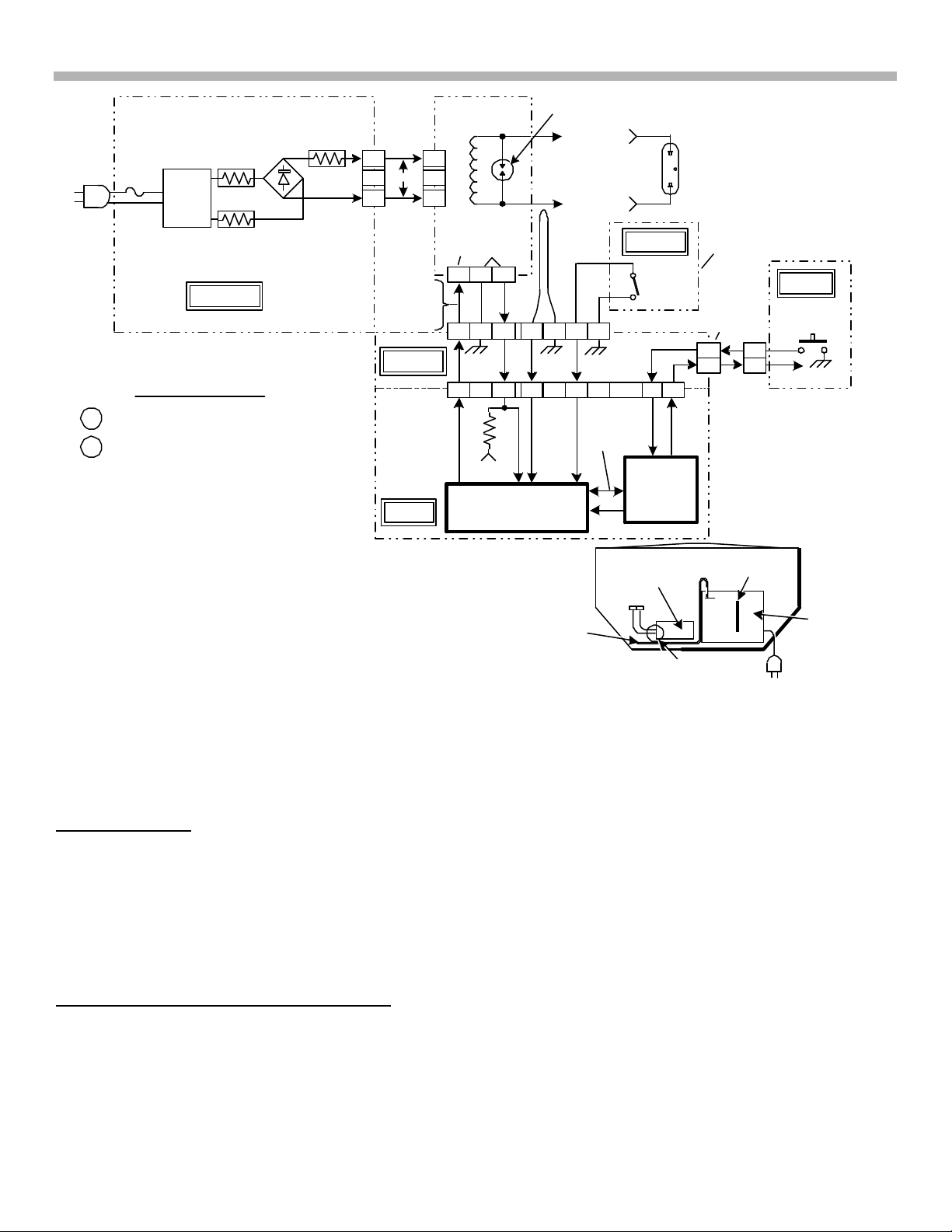
27. Grand Wega Lamp Control
F1601
6.3A
LAMP COMES ON
1 WHEN CN1908/PIN 1 = 5V
2 POWER BLOCK BD.
OUTPUTS 27kV IGNITION
VOLTAGE , THEN 25kV RUN
VOLTAGE
LAMP DEFECTIVE STBY LED BLINKS CONTINUOUSLY
POWER BLOCK BD. DEFECTIVE STBY LED BLINKS 5 TIMES
LAMP COVER SW. OPEN STBY LED BLINKS 3 TIMES
P.S.
R1654
MAIN
R1655
G BD.
New HV Detector Circuit
SPARK GAP
G1
25kV TO GAS
DISCHARGE
HV
DET
PRT
=0V
HV DET
WIRE
LAMP
T BD.
0V
0V
S DATA
CLK
S8001
N/C
CN1908 CN1901
IC9004
MAIN
MICRO
POWER
BLOCK
HV
2
1
R1613
CN1602
POWER
SUPPLY
N/C
-
+
270V
1
2
*
3
255V-
*
350V
CTL=
ON=5V
OFF=0V
A BD.
CN1920/
CN9501
M BD.
POWER
BLOCK BD.
WIRE
COLOR
GRY
WHI
1 233 12 13 4 5
40
40 39 50 49 48
5V
IC9502 LAMP
CONTROL
FIGURE 27-1 - LAMP CONTROL - KF-60DX100
LAMP COVER
BOARD
4 4
7 7
45
4502
G1
H3 BD.
POWER
CN
TV FRONT
6TVP13 1439 4/16/02
STBY LED
M BD.
BLOCK
TV
The purpose of the HV Detector circuit (on the M board) is to identify the cause of no backlight. The front panels
LEDs use this information. The LAMP LED blinks continuously if the lamp is defective or the Standby LED will
blink five times if the HV or control circuitry is bad. Refer to Figure 27-1 for the following HV detector circuit
description:
Normal Operation - At power ON, Main Micro IC9004 instructs Lamp Control IC9502 (both on M board) to output
a HIGH at Ctl (A board, CN1908/pin 1). This HIGH is applied to the Power Block to start the 25kV necessary for
the lamp ignition. If the lamp starts to draw current, the Power Block closes the relay to reduce lamp voltage and
grounds the PRT line (CN1908/pin 3 or the end gray wire on the Power Block).
The PRT (protect) line is a signal to tell the Main Micro the lamp is drawing current (working). When LOW
(0Vdc), the Main Micro in turn unmutes the A/V lines and a picture with sound appears (all within 20 seconds after
turn ON).
Defect - The LAMP LED blinks continuously - The main Micro looks at the PRT signal (CN1908/pin 3) and the
antenna signal to determine if the lamp or Power Block is defective (Table 27-1). When HV appears without a
load (bad bulb), arcing in the spark gap on the Power Block creates RF that is picked up by the nearby antenna
wire. This RF signal is brought back to the A board at CN1908/pin 12. The RF signal only passes through the A
board to get to the M board (CN9501/pin 50) where it is rectified. On the M board, a DC voltage developed after
the RF signal is rectified indicates the presence of HV (normal Power Block operation). If there is HV and no
current draw, the conclusion is that the lamp is bad so the Main Micro continuously blinks the front panel LAMP
LED.
60
Page 63
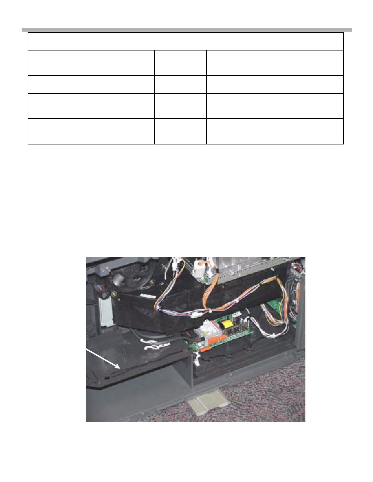
27. Grand Wega Lamp Control
Lamp LED blinks Continuously (HV OK.
Table 27-1 - How the Main Micro Determines if the Lamp or Circuitry is Bad
Condition PRT (Protect)
CN1908/pin 3
Normal Low (0Vdc) None
High (5Vdc) Yes at power ON and repeats every 5
Lamp bad)
Standby LED blinks 5 times (No HV,
Power Block, PS fuses, or M board bad)
High (5Vdc) None
Visual Arcing at G1/ RF at CN1908/pin 12
seconds later until TV shutdown (3 mins.).
Defect – The Standby LED blinks five times – At power ON when the Power block is instructed to turn ON (HIGH
@ white wire to Power Block / CN1908/pin 1), but no current is drawn (HIGH at end gray wire / CN1908/pin 3),
the lamp or the Power Block is defective. To determine which is defective, the antenna signal (explained in the
last paragraph) is used by the Main Micro only when the PRT line (CN1908/pin 3) remains HIGH (no lamp
current).
During this defect, PRT = HIGH forces the Main Micro IC9004 to request information about the presence of HV
via serial data from Lamp Control IC1952. If RF (HV) is not detected, the Main Micro keeps the audio and video
muted, blinks the Standby LED blink five times and shuts down the TV in three minutes.
HV antenna positioning
After repairs, reposition the black HV antenna near one of the HV leads as shown in Figure 27-2. If it is not
positioned as shown, the LAMP LED will NOT flash during a lamp defect.
HV
ANT
WIRE
FIGURE 27-2 - HV ANTENNA POSITION
61
Page 64
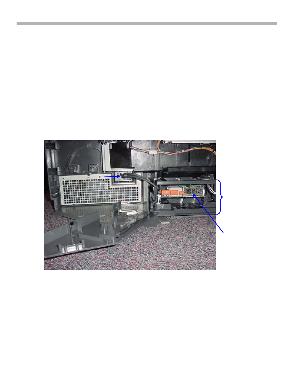
27. Grand Wega Lamp Control
2. Lamp ON Time Display
The time the lamp is ON in hours is stored in the service mode within the “Option-E” category.
1. Enter the service mode (remote = Display, 5, Vol +. Power ON).
2. Use the 5 button to locate the Option-E category. Button 5 moves up to Option E from the bottom of the list.
3. Change this first “Lamp Time” item data from 0 to 1 using the 3 button.
4. The lamp time is displayed on the screen in hours.
Lamp On Time Reset
5. To reset the time, follow the procedure above, return to step 3 (“Lamp Time” item) but change the data to “0”
and press MUTE, then Enter. The hours will reset to 000.
3. Power Block Location & Removal
From the back of the TV set, the Power Block is located at the bottom center. Figure 27-3 shows the Power
Block (right) and its HV wires terminated at the lamp socket (left).
HV Lamp Socket
Power Block
Assembly
Power Block
FIGURE 27-3 - HV LAMP CONNECTOR
The Power Block assembly and HV connector is one assembly and must be removed together.
1. Remove the two screws from the HV socket as shown in Figure 27-3.
2. Lift the Power Block (as an assembly) up and outward (see Figure 27-4).
3. Remove the top and bottom covers and unplug the two board connectors (not shown).
62
Page 65
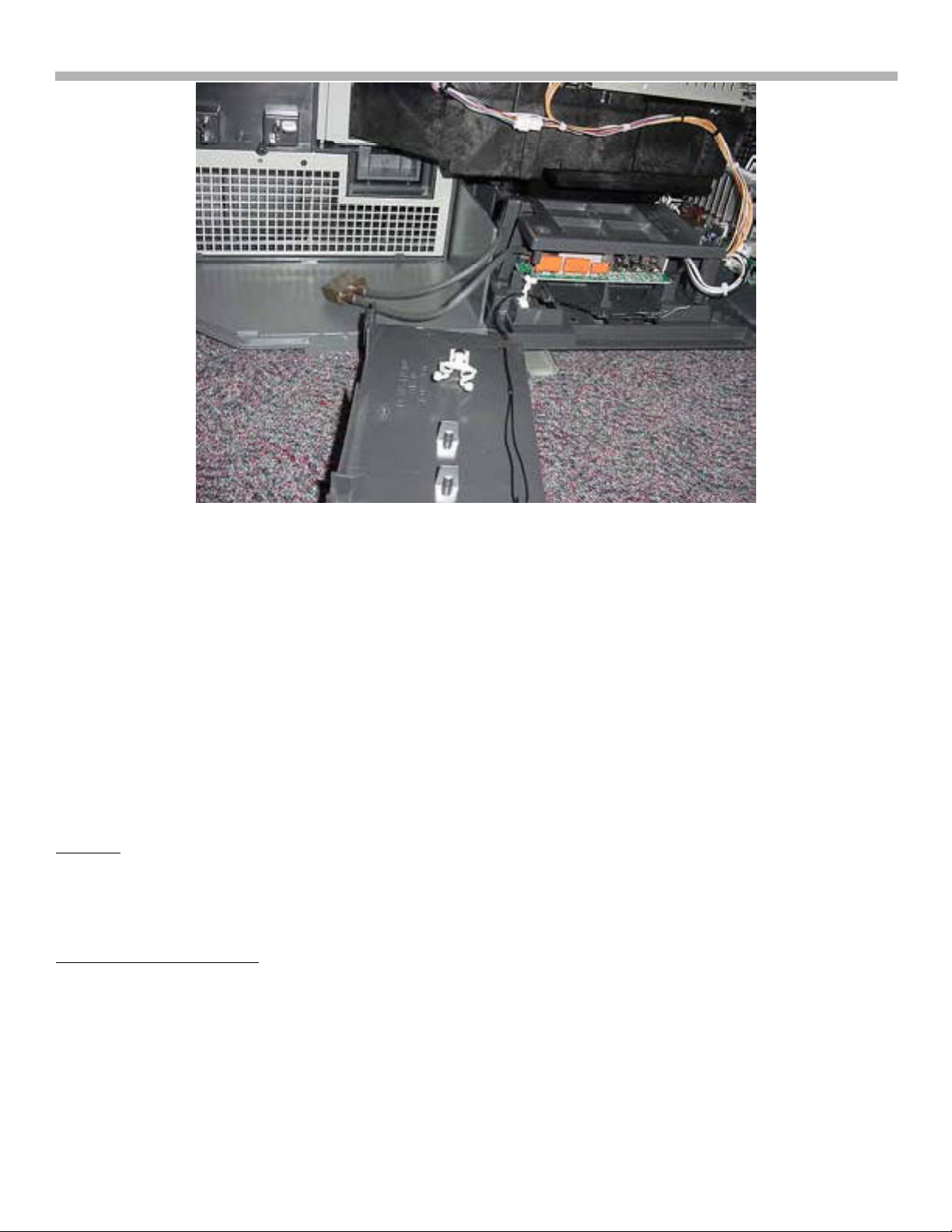
27. Grand Wega Lamp Control
FIGURE 27-4 - COMPLETE POWER BLOCK ASSEMBLY
4. Troubleshooting
Defect – Unreliable backlight starting
As the gas discharge tube reaches the end of life, the most common symptom is unreliable starting at power ON,
especially when the lamp is cold. Replace the lamp.
Defect - No backlight repair procedure
The lamp will not turn ON because of a defective:
• Lamp
• Power block board (no HV)
• Control engine (M board – no turn ON signal).
• Fusible resistor(s) on the power supply G board.
Concept: When the backlight bulb / lamp reaches the end of life and does not ignite, the internal resistance
across its two terminals remain high (open circuit). This causes the HV to climb to 25kV and arc across the spark
gap device (G1) on the Powre block (proving the Power Block and controlling M board are working). The HV
arcing makes an audible frying sound and light is visible. The HV arcing lasts two seconds, stops for five
seconds and repeats until the TV shuts down in three minutes.
Troubleshooting procedure: If the Power Block arcs, the bulb is either defective or not plugged in. No arcing?
Measure the HV control signal input to the white wire of the 3-wire connector on top of the Power Block. If this
CTL input voltage is correct at 5Vdc at TV turn ON (within two seconds), the Powr Block or power supply board
fuses are bad. If CTL is 0Vdc at turn ON, the controlling M board is bad or one of the Fans is not rotating (no fan
causes no lamp ON and shutdown). See the Fan Control Fan Troubleshooting in Chapter 26 or just check the
self-diagnostic Chapter 16.
63
Page 66
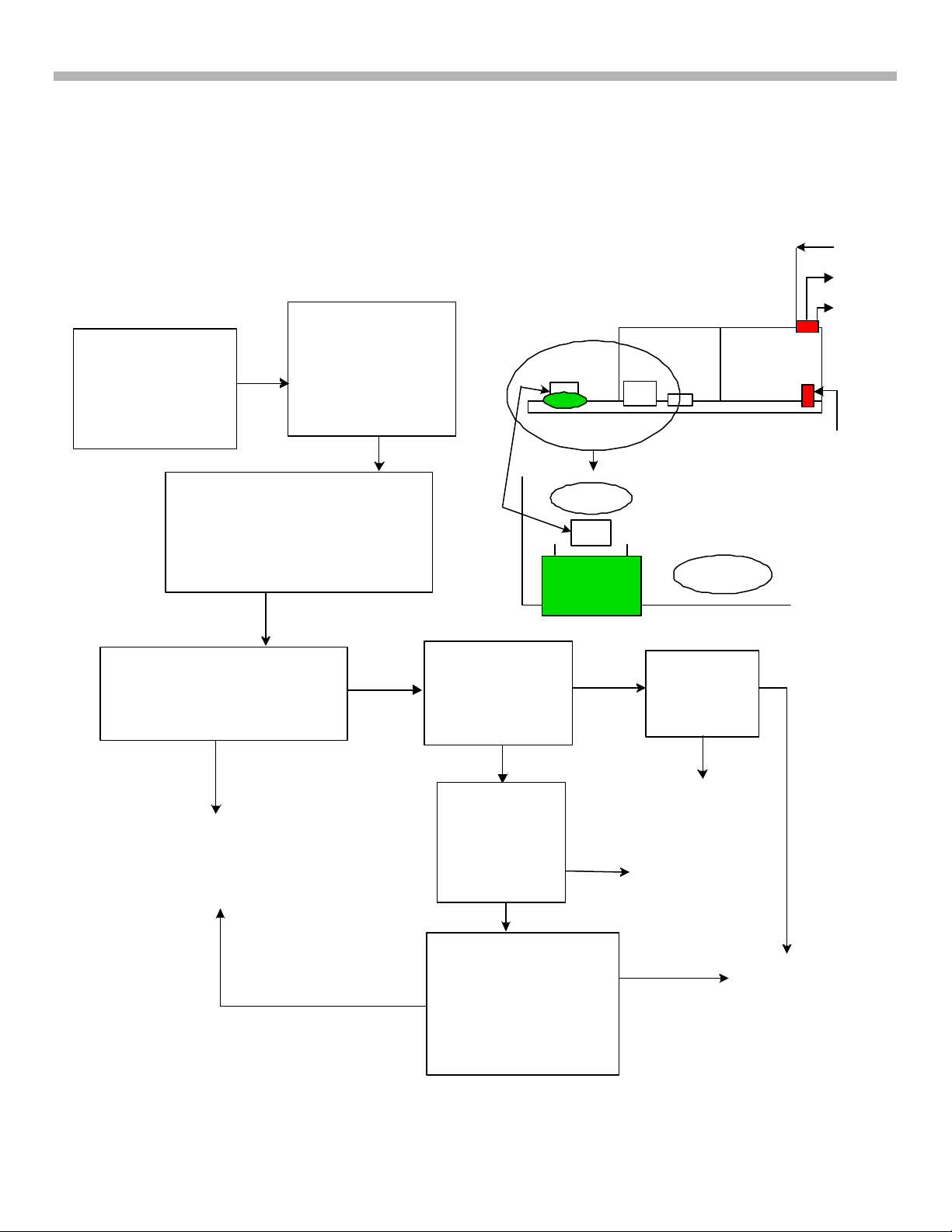
27. Grand Wega Lamp Control
Defect – No backlight repair flow chart:
The following flow chart will help you quickly ID the problem board, but you must be careful. High Voltage at a
very High Current is present (not like a TV’s FBT where there is low current).
Be aware that if the backlight does not start at power ON, the lamp HV circuitry is repeatedly instructed to try to
turn ON for two seconds and again five seconds later until the TV shuts down. Therefore you must keep away
from the HV when the TV is plugged into AC. To use this flow chart, you will need a DVM to determine which
board is defective.
Ctl
Symptom = Fan ON
but Backlight OFF.
Standby LED blinks,
A/V muted. TV shuts
down after 3 minutes.
WARNING - At TV turn ON, LETHAL
HV at high current (unliked an FBT)
outputs the Power Block. Observe
spark gap cylinder G1 for HV from two
feet away or more. Close front panel
lamp door so HV can start
Watch the G1 spark gap behind
C101. Turn ON the TV. Do you
hear a HV frying noise or see light
from the G1 body?
With the TV
unplugged, bend down
the left C101 capacitor
on the Power Block as
shown to make
cylinder G1 visible,
No
G1
Does Ctl (white
wire) change to
5Vdc * at TV turn
ON?
Power Block - Side View
C100
G1
C101
No
C102
Corner - top view
Replace M
board. Does
Lamp light?
Gnd
prt
+/-
Connector
Yes
The circuitry is working.
Unplug the TV.
Inspect the HV socket for
corrosion (white powder).
Replace the UL200 Lamp.
* This Ctl voltage will only
be present for 2 seconds
and then again for 2 more
seconds 5 seconds later.
FIGURE 27-5 - DEFLECT - BACKLIGHT DOES NOT LIGHT
Yes
Yes
Is there 255-350
Vdc Across the
Power Block +/connector?
Yes
Remove 2 screws and
unplug the lamp socket.
Lay the HV connector
down away from metal or
people. Turn ON the TV.
Is there arcing at G1?
No
64
Finished
Replace Power
Supply G board
No
Replace the
Power Block
4/16/02
Page 67
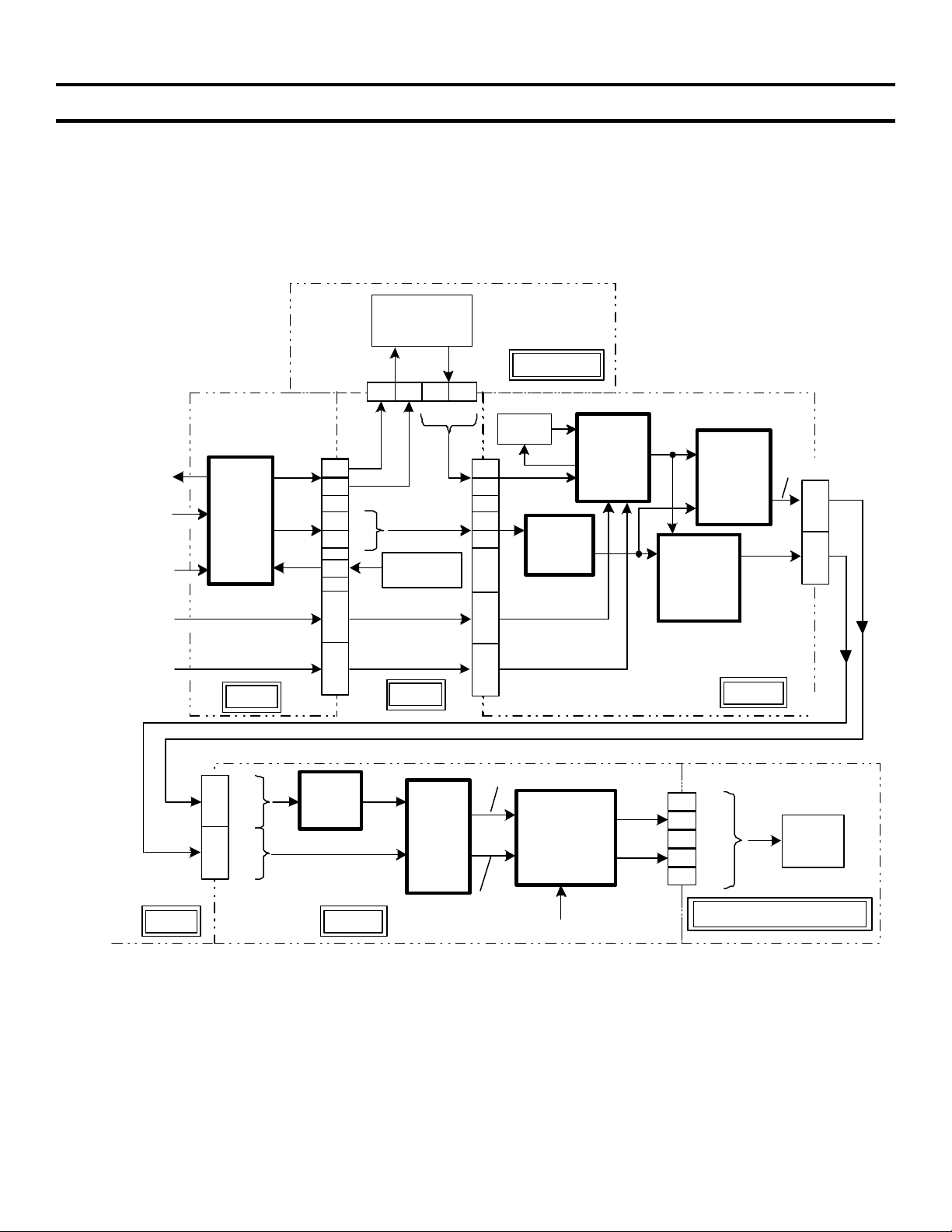
28. Grand Wega Video Process
Chapter 28 - Video Process
Video Signal Flow
The video signal flow is shown in Figure 28-1. The video signal is input the U board, through the BC and BB
boards to the final C board within the sealed optical unit optical assembly. The A board is an interconnect board
that passes the video signal from one board to another and performs the initial TV tuner function. Table 28-1
explains the function of each board and their inputs/outputs.
3D COMB
FILTER
TV OUT (V)
S VIDEO
(Y,C)
COMPOSITE
VIDEO (V)
COMPONENT
VIDEO
(R,Cr,Cb)
SEL
IC2004
A/V
SW.
U BD.
CN2001/
CN1901
CN2001/
CN1917
MAIN
SUB
A29
C29
A20
C20
C1
A15
A16
A17
C12
A13
C14
V
C
Y
C
1 15
TUNER
A BD.
3
Y
SUB
5
C
C30
C31
C10
C13
C12
C11
C7
C6
C9
C8
B C 4 BD.
CCD
MAIN
IC3009
CCD
VID 5
CN1924/
CN3001
IC3004
VID 6
YCT
IC3006
IC3011
MILD
SEL
YCT
SEL
CN3001/
CN1924
BC BD.
SEL
MAIN
C20
C22
C21
C29
C27
C28
SEL
MAIN
20
24
22
40
36
38
Y
Cb
Cr
Y
Cb
Cr
IC304
DRC
CN1923/
A BD. BB BD.
CN704
FIGURE 28-1 - VIDEO PROCESS - KF60DX100
IC509
MID
VIDEO
IC701
RGB
DECODER
SYNC
OSD FROM M BD.
65
CN702/CN5005
1
R
3
G
5
B
7
V
9
H
LCD
PANEL
C BD./OPTICAL UNIT
4/15/029TVP131447
Page 68
Table 28-1 - Video Circuit Board Inputs / Outputs
28. Grand Wega Video Process
Board
U •
A •
BC4 •
BC
BB •
Input(s) Board Function Output(s)
TV Tuner, S Video
•
Composite Video
• Component video inputs.
VHF antenna
Composite Video (V) or
S video (Y & C)
• S Video (Y & C)
•
Component video inputs.
Main picture component
video
•
Sub picture component
video
•
NTSC Input switching
•
Component video pass through.
•
TV tuner and control
•
Interconnecting video boards
Comb filter separates the Y & C
from the composite V (video)
signal.
• Creates a Main and Sub
picture video path
• Channels video into the Main
(DRC) & Sub picture video
paths.
•
Switches picture location
when NTSC video is input.
•
Adds User Menu into the
video path.
•
TV Output to rear panel,
•
Composite S video to BC4
bd.
•
Component video to BC Bd.
Various
•
Separate Y & C Outputs for
the BC Bd.
• Main picture component
video
• Sub picture component
video
•
RGB and Sync Output to
the (LCD) light box
assembly.
C •
RGB and Sync input
Independent RGB processing
into separate RGB LCD panels.
•
Display outputs onto mirror.
Troubleshooting
Video symptoms can be classified into three groups:
• White Screen – Video path open on any video signal board.
• Black Screen - BB board or optical unit are suspect.
• Video Screen Distortion – Narrow down by checking the features.
In a conventional TV, a loss of video signal results in a white screen with normal TV sound. This is also true in
this LCD projection TV. However, if the screen is dark with normal sound, either the LCD optical unit or the
previous BB circuit board may be bad.
On the other hand, a dark screen without sound indicates both video and audio muting and not a problem in the
video chain. Muting is caused by: 1) the Main Micro because of: a communications problem with another IC; 2)
a fan defect; 3) a lamp circuit defect; or 4) an audio output failure, which will also cause TV shutdown. Muting the
A/V is not a video failure. A video failure does not affect the sound.
White Screen
If the screen is white, there may be no input to the light box. Press the Menu button. If an OSD menu appears,
the optical unit is good and the previous stages are bad (BC or BB board). If no OSD, use Table 28-2 and a DVM
to verify these inputs to the optical unit before changing it. Measure the input voltage at CN5002 and verify RGB
input signal at CN5005. If the input voltages and signals are both present, the optical unit is suspect.
66
Page 69
28. Grand Wega Video Process
FIGURE 28-2 - OPTICAL UNIT CONNECTORS (TOP VIEW)
Table 28-2 – Optical Unit Input Voltages and Signal Levels (color bar input)
Input Voltage
(from G board)
CN5002/pin 1
(white)
CN5002/pin 3,4
(orange)
CN5002/pin 7,8
(orange)
CN5002/pin 11
(orange)
CN5005/pin 9
Level Input Signal
(from BB board)
- 7Vdc CN5005/pin 1
(Blue signal)
5Vdc CN5005/pin 3
(Green signal)
3.3Vdc CN5005/pin 5
(Red signal)
15Vdc CN5005/pin 7
(Vert sync)
(Horiz sync)
Level
2.5Vp-p
2.0Vp-p
2.4Vp-p
5Vp-p
5Vp-p
Black Screen
If the screen is black, the optical unit or BB board may be bad. First, see if the Menu feature functions. Press the
Menu button on the remote control. If the screen displays the OSD menu, the optical unit assembly is working
and the BB board is suspect.
If there is still no display, remove the input power to the optical unit by unplugging the power connector CN5002
(see Figure 28-2). If the screen becomes white, the BB board is bad. A white screen is normal if the optical unit
loses power (the optical unit passes all the backlight). If the screen remains black, the optical unit is bad.
CN5002
Power In
(orange)
CN5005 RGB, sync in (gray)
CN5001 DATA, blanking (red)
CN5004 S Data (white)
Video Screen Distortion
Distortion, defects or interference can enter the video chain at any of its five boards used in the video processing
chain. You can use some features to help determine where the video problem is. The features most helpful in
isolation are: the On Screen Display (OSD) menu, the MILD picture mode, activity in Video 5/6 inputs and the
Twin View Mode.
On Screen Display to Check the Optical Unit
You can use the On Screen Display Menu to check the circuitry after the BB board. If the screen displays no
(black or white) picture or a distorted picture, press the Menu button on the remote control. If the screen displays
the OSD menu undistorted, the optical unit assembly is working (along with the OSD circuit in the later stages of
the BB board where the OSD circuit is). See Figure 14-1. If the OSD Menu is present, this also means the BB
and BC boards are the primary suspects causing the video distortion.
Video Problem that does not appear in the MILD Picture Mode
When watching an NTSC program from the tuner or video 1-4 inputs, this video signal passes through the DRC
and MID circuits on the BB board. By selecting the MILD picture setting, this video signal is diverted around the
DRC stage.
Therefore, if the NTSC video problem does not appear when selecting the MILD mode, the problem is on the BB
board in the DRC circuit.
67
Page 70
28. Grand Wega Video Process
Video Problem Only with a single input or feature
Table 28-3 lists a feature and/or input that has a picture distortion and the corresponding board that is most likely
responsible for the problem. For example, if a video problem only appeared while watching a TV station but not
in a video input, the most likely cause is shown by the #1 under the A board column (A board defect). The # 2
under the U board column indicates a lesser possibility that the A/V selector IC is defective on the U board, a
second board choice. The remaining boards that process the other input signals are not suspect because the
problem does not appear with another input.
Table 28-3 - Board causing a Video Problem
Video Problem
appears only with
TV Tuner 2 1
Video input 1-4 1 3 2
S Video 1-3 1 2
Video 5, 6
(Component Video)
TV Out 1
Any input including
the OSD.
Mild Menu setting * 1
CCD 2 1
OSD 1
Twin Picture 1 1
* The “Mild” Menu video selection (Vivid/Standard/Movie/Mild) routes the signal around the Digital Reality
Creation Circuitry, feeding it directly into the MID IC. Noisy NTSC input signals can fool the DRC circuit
into introducing false picture improvements, adding to the noise, making the MILD mode useful with noisy
signals.
U board BC board BC4 board BB board Optical Unit
Assembly
1 1
2 1
A board
Using Twin View Mode to Locate the Video Problem
Twin View Signal Path Concept
This TV has the ability to display two pictures side by side on the same screen. In the “Twin View” picture mode
(Figure 28-3), both main and sub signal paths are used to produce the dual picture. The difference in the two
paths is that the main path contains the DRC picture enhancement circuit (left picture). Both main and sub
picture paths arrive at the MID circuit (BB board) to be assembled into a single picture. The rules for this Twin
View video processing are:
1. The DRC circuit can only be used for a 480i (NTSC) input signal.
2. The DRC picture will always be the larger picture.
3. When both NTSC pictures are the same size, the LEFT picture will be the DRC picture (using the main signal
path).
4. When there is a High Definition (HD) picture input (video 5 or 6), the RIGHT picture will be the DRC picture.
5. The RIGHT picture CANNOT select a HD (video 5 or 6) input.
Video switching in both the BC and BB boards will ensure these rules are followed. Figure 28-3 shows the
displayed signals with different inputs.
68
Page 71
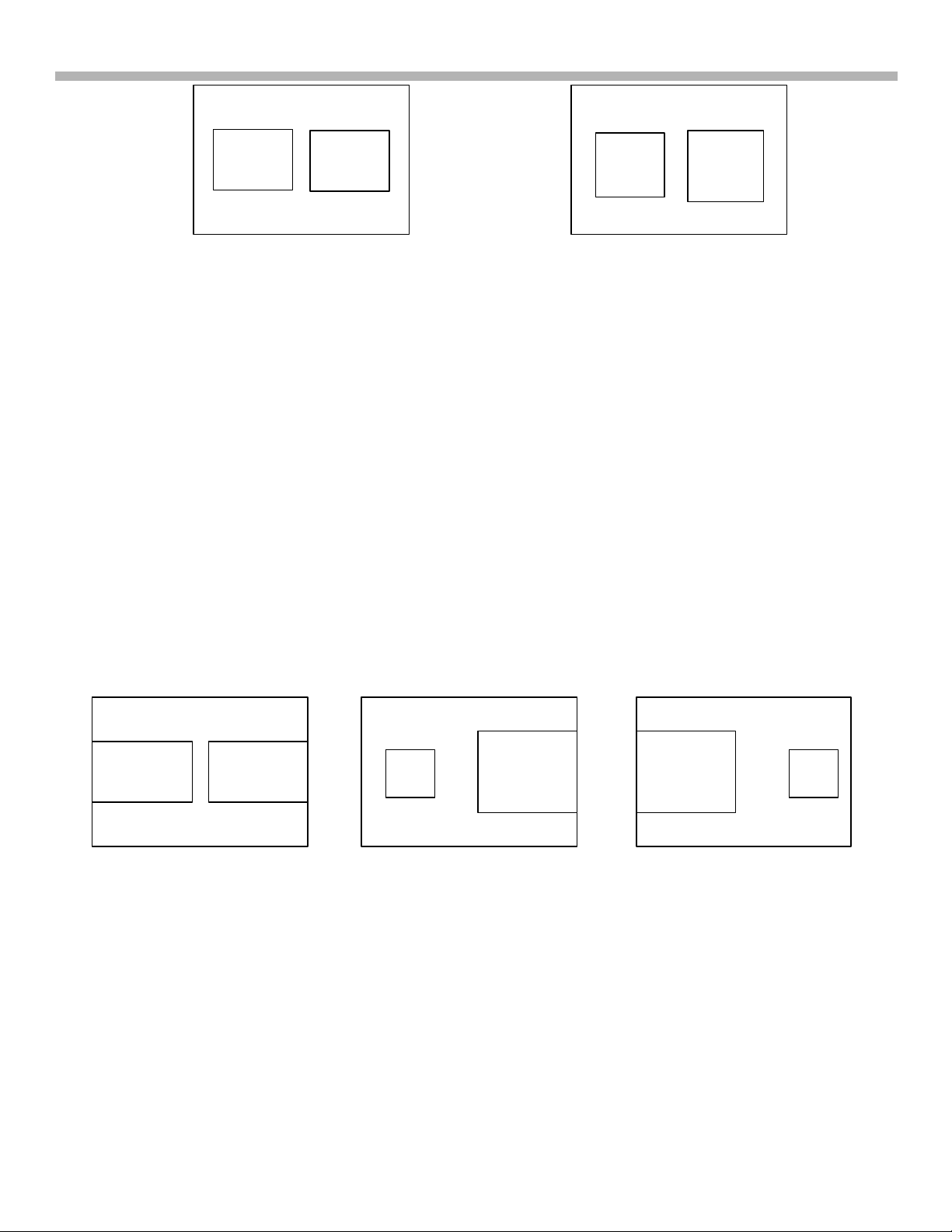
28. Grand Wega Video Process
Main/
DRC
Two NTSC (480i)
pictures displayed
Sub
pix
HD
Left = High Definition
(480p, 720p, 1080i) &
Right = NTSC (480i)
Main/
DRC
FIGURE 28-3 - VARIOUS TWN PICTURE DISPLAYS WITH NTSC AND/OR HIGH
DEFINITION (HD) SIGNALS. (HD INPUT FROM VIDEO 5 OR 6)
Two 480i (NTSC) Pictures Input
Refer to Figure 28-4, which indicates where the larger picture’s signal comes from. When either both pictures
are the same size (Figure 28-4a) OR if the LEFT picture is the larger picture (Figure 28-4b), the DRC circuit (BB
board) is used to improve the quality of the 480i (NTSC) signal. The main picture from IC3006 (BC board) is
positioned on the LEFT side (by the MID circuit on the BB board).
When the picture on the LEFT becomes the larger (Figure 28-4c), the Main and Sub input signals switch (BC
board) and the MID process (IC509, BB board) also switches the picture position. This double signal crossing
allows the channels to be at the same place on the screen (but the signal paths are different). This switching is
done to ensure the high-quality DRC signal is employed by the larger picture.
As the user increases the picture size from smaller to larger, a slight delay occurs when the right picture just
begins to enlarge. This allows both the SEL switch ICs (BC board) and the MID circuit (BB board) to switch
positions. The picture freezes for a moment until both switches have been made, and then the picture frame
continues to increase in size.
Sub pix
IC3011
Main pix
Main pix
IC3006
a b c
S
from
IC3006 &
DRC
Main pix
from
IC3006 &
DRC
S
FIGURE 28-4 - TWIN PICTURE MODE, ANALOG INPUTS
One 480i (NTSC) Picture Input and
One HD (480p/720p/1080i) Picture Input
When one twin view picture contains a HD signal, that HD picture always takes the SUB signal lower path (Figure
28-1) into the MID IC509 and appears on the LEFT side of the screen.
69
Page 72
28. Grand Wega Video Process
Conclusion / Troubleshooting
What does all this mean? How can we use this video path switching to determine which board contains the video
problem? Refer to the flowchart in Figure 28-5 to determine if the problem is in the A, U, BC, BC4, BB board or
the optical unit optical assembly just by noting where the video problem moves as you increase the picture size
in the Twin View Mode.
Does the NTSC
picture have a
picture defect?
Does the problem
appear in all inputs
(video / component)?
No
If the problem is
in the Tuner and
video 1-4, change
the U board.
If the problem is in
component video,
change the BC board.
FIGURE 28-5 - FLOW CHART
ISOLATING THE VIDEO PROBLEM USING THE TWIN
PICTURE MODE
Yes
Press the "Twin Mode"
button on the remote
control and make the
RIGHT picture larger.
Does the problem remian
where it is on the screen?
No. Moves to a picture
Do both pictures have
the same problem?
No
Make the LEFT picture
larger. Where is the
defect?
Yes
Yes
Same
Pix
If the video problem is
stationary, the optical unit
optical assembly is
defective. Replace it.
Change the
BB board.
(MID circuit problem).
Change the
BB board.
(DRC circuit problem).
Different
Pix
BC and BC4 boards are both
suspect. Unplug the BC4 board
and jump the A board's
CN1901/pin 1 to pins 3 and 5.
Problem gone?
70
Yes
No
Change BC4 board.
Change BC board.
4/16/02
Page 73
TVP130402
is a trademark of Sony Electronics
Sony Electronics Inc.
EMCS - A Service Company
1 Sony Drive
Park Ridge, New Jersey 07656
All Rights Reserved ©2002
04/22/02
 Loading...