

Sony KV-SZ252M50, KV-SZ252M61, KV-SZ252M81, KV-SZ252N50, KV-SZ252N60 Schematic
REVISION HISTORY
BX1L
CHASSIS
MODEL
KV-SZ252M50
KV-SZ252M61
KV-SZ252M81
KV-SZ252N50
KV-SZ252N60
NO. SUFFIX DATE SUPP / CORR DESCRIPTION
1 -01 2007/04 _ _ 1st Issue
PART NO.: 9-872-963-01
SERVICE MANUAL
BX1L
CHASSIS
MODEL COMMANDER DEST. CHASSIS NO.
KV-SZ252M50 RM-GA002 E SCC-V66P-A
KV-SZ252M61 RM-GA002 GE SCC-V44U-A
KV-SZ252M81 RM-GA002 Middle East SCC-V83H-A
KV-SZ252N50 RM-GA002 Philipines SCC-V80K-A
KV-SZ252N60 RM-GA002 Philipines SCC-V80J-A
MODEL COMMANDER DEST. CHASSIS NO.
RM-GA002
TRINITRON
®
COLOR TV

KV-SZ252M50/M61/M81/N50/N60
RM-GA002
TABLE OF CONTENTS
Section Title Page
SELF DIAGNOSTIC FUNCTION ........................................... 3
1. DISASSEMBLY
1-1. Rear Cover Removal..................................................5
1-2. Speaker Removal ....................................................... 5
1-3. Chassis Assy Removal ............................................... 5
1-4. Service Position ......................................................... 5
1-5. A and H2 Board Removal ......................................... 5
1-6. Picture Tube Removal................................................ 6
2. WIRE DRESSING
2-1. Lead Assy, Jumper Wire Dressing at A board...........7
2-2. Lead Assy, Jumper Wire Dressing at A board
(only for Audio 6+6 Non DSP models) .................... 7
2-3. Wire Dressing at A and H2 board ............................. 7
2-4. Dressing of Conn Assy, 4P VH ................................. 8
2-5. Dressing of Conn Assy, 5P YUV ............................... 8
2-6. Dressing of Conn Assy, 4P VM and
Connector Assy, 5P Front In...................................... 8
2-7. Installation and Dressing of Earth Assy Coating ...... 8
2-8. Installation and Dressing of Earth Assy Coating ...... 9
2-9. Insertion of Lead Assy, H Static................................ 9
2-10. Dressing of Conn Assy, 5P Front In .......................... 9
2-11. Dress Lead Assy, Earth and Conn Assy,
5P In with Purse Lock Ø 5 ...................................... 10
2-12. CV Board Connector Assy Wire Dressing.............. 10
2-13. Connector Assy Wire Dressing................................10
2-14. Connector Assy Wire Dressing................................11
2-15. Overall V iew of Rotation Coil Conn Dressing ....... 11
2-16. Overall View of Lead Assy, G2; Lead Assy, Focus
and Rotation Coil Conn Dressing ........................... 11
2-17. Dress Lead Assy, Speaker to Rotation Coil using
Purse Lock Ø 9 ........................................................ 12
2-18. Dressing of PF Board Conn Assy (for models
with PF board only) ................................................. 12
2-19. Cap Assy, High Voltage Installation ........................12
2-20. HV Cap Assy Wire Dressing ................................... 13
2-21. AC Power Cord Wire Dressing ............................... 13
Section Title Page
4. CIRCUIT ADJUSTMENTS
4-1. Adjustment With Commander ................................18
4-2. Adjustment Method ................................................19
4-3. Picture Quality Adjustment .................................... 36
4-3-1. P Max/Contrast Adjustment .........................36
4-3-2. Sub Color Adjustment ..................................36
4-3-3. Sub Hue Adjustment ....................................36
4-4. Geometry Adjustment .............................................37
4-4-1. H-Trapezoid Adjustment ..............................37
4-4-2. Normal Mode 50Hz/60Hz ............................ 37
4-4-3. Wide Mode 50Hz/60Hz
(V Compression Adjustment)................................ 37
5. DIAGRAMS
5-1. Block Diagram ......................................................... 38
5-2. Circuit Boards Location .......................................... 39
5-3. Schematic Diagram Information ............................. 39
5-3-1. A Board — (Block 001)............................... 40
5-3-2. A Board — (Block 002)............................... 42
5-3-3. A Board — (Block 003).............................. 44
5-3-4. A Board — (Block 004)............................... 46
5-3-5. A Board — (Block 005)............................... 48
5-3-6. A Board — (Block 006)............................... 50
5-3-7. A Board — (Block 007)............................... 52
5-3-8 CV Board Schematic Diagram ..................... 53
5-3-9. H2 Board Schematic Diagram...................... 55
5-4. Voltage Measurement and Waveform...................... 57
5-5. Printed Wiring Boards ............................................. 61
5-6. Semiconductors........................................................ 67
6. EXPLODED VIEWS
6-1. Chassis ..................................................................... 69
7. ELECTRICAL PARTS LIST .......................................... 71
OPERATING INSTRUCTIONS
3. SET-UP ADJUSTMENTS
3-1. Beam Landing Adjustment...................................... 14
3-2. Convergence Adjustment.........................................15
3-3. Focus Adjustment .................................................... 17
3-4. G2 (SCREEN) Adjustments ....................................17
3-5. Sub Bright Adjustment ............................................ 17
3-6. White Balance Adjustment...................................... 17
CAUTION
SHORT CIRCUIT THE ANODE OF THE PICTURE TUBE AND THE
ANODE CAP TO THE METAL CHASSIS, CRT SHIELD, OR
CARBON PAINTED ON THE CRT, AFTER REMOVING THE
ANODE.
SAFETY-RELATED COMPONENT WARNING!!
COMPONENTS IDENTIFIED BY SHADING AND MARK ! ON THE
SCHEMATIC DIAGRAMS, EXPLODED VIEWS AND IN THE
PARTS LIST ARE CRITICAL TO SAFE OPERATION. REPLACE
THESE COMPONENTS WITH SONY PARTS WHOSE PART
NUMBERS APPEAR AS SHOWN IN THIS MANUAL OR IN
SUPPLEMENTS PUBLISHED BY SONY.
– 2 –
KV-SZ252M50/M61/M81/N50/N60
SELF DIAGNOSTIC FUNCTION
The units in this manual contain a self-diagnostic function. If an error occurs, the STANDBY Indicator will automatically
begin to flash.
The number of times the STANDBY Indicator flashes translates to a probable source of the problem.If an error symptom
cannot be reproduced, the remote commander can be used to review the failure occurrence data stored in memory to
reveal past problems and how often these problems occur.
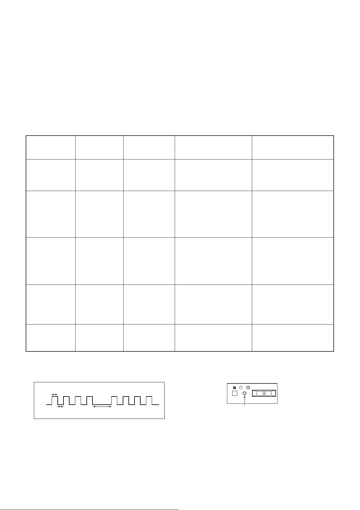
1. DIAGNOSTIC TEST INDICATORS
When an error occurs, the STANDBY Indicator will flash a number of times to indicate the possible cause of the
problem. If there is more than one error, the Indicator will identify the first of the problem areas.
Result for all of the following diagnostic items are displayed on screen. No error has occured if the screen displays a “0”.
RM-GA002
Diagnosis
Item
Description
• No Power
• +B overcurrent
(OCP)
•Vertical NG.
• IK (AKB)
No. of times
STANDBY
Indicator flashes
Does not light
2 times
4 times
5 times
Diagnostic Result
on screen display
—
2 OCP:0
2 OCP:1 ~ 255
4 VSTOP:0
4 VSTOP:1 ~ 255
5 AKB:0
5 AKB:1 ~ 255
Probable
Cause
Location
•Power cord is not plugged
in.
• Fuse is burned out (F4101)
(H2 Board)
• H.OUT (Q511) is shorted.
(A board)
• IC751 is shorted.
(C/CV Board)
• +13V is not supplied.
(A Board)
• IC503 voltage list is faulty.
(A Board)
• Video OUT (IC751) is faulty.
(CV Board)
• IC001 is faulty. (A Board)
• Screen (G2) is improperly
adjusted.
Detected
Symptoms
•Power does not turn on.
•No power is supplied to the
TV.
•AC power supply is faulty.
•Power does not turn on.
•Load on power line is
shorted.
•Has entered standby state
after horizontal raster.
•Vertical deflection pulse is
stopped.
•Power line is shor ted or
power supply is stopped.
•No raster is generated.
•CRT cathode current
detection reference pulse
output is small.
• Supply Voltage
Protection
8 times
8 SUP:0
8 SUP:1 ~ 255
2. STANDBY INDICATOR BLINKING PROCESS
Lamp ON 300ms
Lamp OFF 300ms
The example above represents for 4 times blink
Lamp OFF 3 seconds
• IC604 faulty.
• IC607 faulty.
•No power supply to CRT
ANODE.
•No RASTER is generated.
3. STANDBY INDICATOR ON TV FRONT PANEL
Standby indicator
– 3 –
KV-SZ252M50/M61/M81/N50/N60
RM-GA002
4. SELF DIAGNOSTIC SCREEN DISPLAY
SELF DIAGNOSTIC
2 : 000
3 : N/A
4 : 000
5 : 001
8 : 002
101 : N/A
5. HANDLING SELF DIAGNOSTIC SCREEN DISPLAY
No. Description Method
1. Display self diagnostic screen [Display] t [Channel ] t [Volume ] t [Power / TV]
2. Stop standby flash i) Turn off power switch on main.
3. Clear fault result In self diagnostic screen, press [Channel ] t -
4. Quit self diagnostic screen Turn off power switch of remote commander or main unit.
"0" means no fault has been detected.
"1" means a fault has been detected.
"2" means two faults has been detected.
"N/A" means not available for this models.
5
Note: The above must be performed while TV is on standby mode.
ii) Unplug power cord from the outlet.
8
Note: Diagnostic results display on screen is not automatically cleared. Therefore,
clear result after completion of repair.
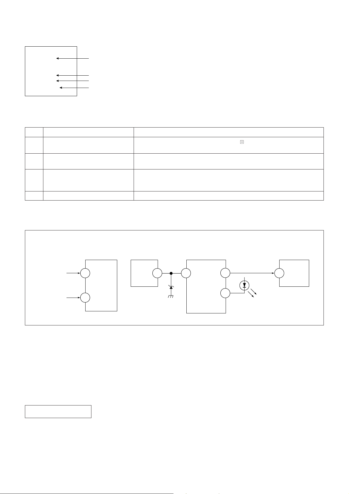
6. SELF-DIAGNOSTIC CIRCUIT
A BOARD
IC003
MEMORY
5
SDA
FROM
CV BOARD
IC751 PIN 5
A BOARD
FROM
Q816
COLLECTOR
A BOARD
IC001
Y/CHROMA JUNGLE
IK
32
EHT0
A BOARD
IC503
V.OUT
F.B-PLS
A BOARD
IC001
SYSTEM
SDA1
3 1384
V.GUARD
RED LED
99
122
DISPLAY
[+B overcurrent $OCP%] Occurs when an overcurrent on the +B(135V) line is detected by pin 32 of IC001 (A board).
If the voltage of pin 32 of IC001 (A board) is more than 4V, the unit will automatically go to
standby.
[V-PROTECT] Occurs when an absence of the vertical deflection pulse is detected by pin 13 of IC001
(A board).
[IK $AKB%] If the RGB levels* do not balance within 15 sec after the power is turned on, this error will be
detected by IC001 (A board). TV will stay on, but there will be 5 times LED blinking.
POWER SUPPLY NG (+5V)
for VIDEO PROCESSOR
Occurs when IC001 internal HV protect detects an abnormal H-Pulse (frequency) due to
improper power supply to IC001. TV cuts off high voltage power of anode CRT. No picture will be
detected. eg: IC602, IC604 go faulty.
* (Refers to the RGB levels of the AKB detection Ref pulse that detects IK.)
– 4 –
SECTION 1
DISASSEMBLY
KV-SZ252M50/M61/M81/N50/N60
RM-GA002
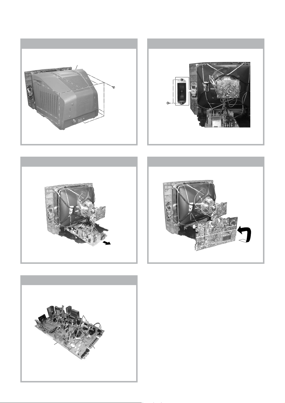
1-1. REAR COVER REMOVAL
2 Rear cover
1 Nine screws
(+BVTP 4 × 16)
1-2. SPEAKER REMOVAL
1 Two screws
(Tapping screw)
(+PWH 4x16)
1-3. CHASSIS ASSY REMOVAL 1-4. SERVICE POSITION
1-5. A AND H2 BOARD REMOVAL
1 Two hooks
3 A Board
2 H2 Board
– 5 –
KV-SZ252M50/M61/M81/N50/N60
RM-GA002
1-6. PICTURE TUBE REMO VAL
Note:
• Please make sure the TV set is not in standing position bef ore removing necessary CRT support located on bottom
right and left.
1) Remove the rear cover.
2) Unplug all interconnecting leads from the Deflection yoke, Neck assy, Degaussing Coil and CRT grounding strap.
Remove Chassis Assy.
3) Place the TV set with the CRT face down on a cushion jig.
qd Screw Tapping
7+ Crown Washer (x4)
0 Earth Coating Assy
9 Degaussing Coil
8 Spring Tension(x2)
Removal
qs Supports CRT (x2)
Removal
qa Loosen the Deflection Yoke
fixing screw and remove
4 Anode Cap Removal
7 Band, DGC Removal
6 Loosen the Neck Assembly
fixing screw and remove
Neck Assy
5 CV Board Removal
• REMOVAL OF ANODE-CAP
Note:
• After removing the anode, short circuit the anode of the picture tube and the anode cap to the metal chassis, CRT
shield or carbon paint on the CRT.
• REMOVING PROCEDURES
a
a
1 Turn up one side of the rubber cap in the direction
indicated by the arrow a.
b
b
2 Using a thumb pull up the rubber cap firmly in the direc-
tion indicated by the arrow b.
c
Anode Button
3 When one side of the rubber cap is separated from the
anode button, the anode-cap can be remo ved by
turning up the rubber cap and pulling it up in the
direction of the arrow c.
• HOW TO HANDLE AN ANODE-CAP
1 Do not damage the surface of anode-caps with
sharp shaped objects.
2 Do not press the rubber too hard so as not to
damage the inside of anode-cap.
A metal fitting called the shatter-hook terminal is
built into the rubber.
3 Do not turn the foot of rubber over too hard.
The shatter-hook terminal will stick out or damage
the rubber.
– 6 –
KV-SZ252M50/M61/M81/N50/N60
RM-GA002
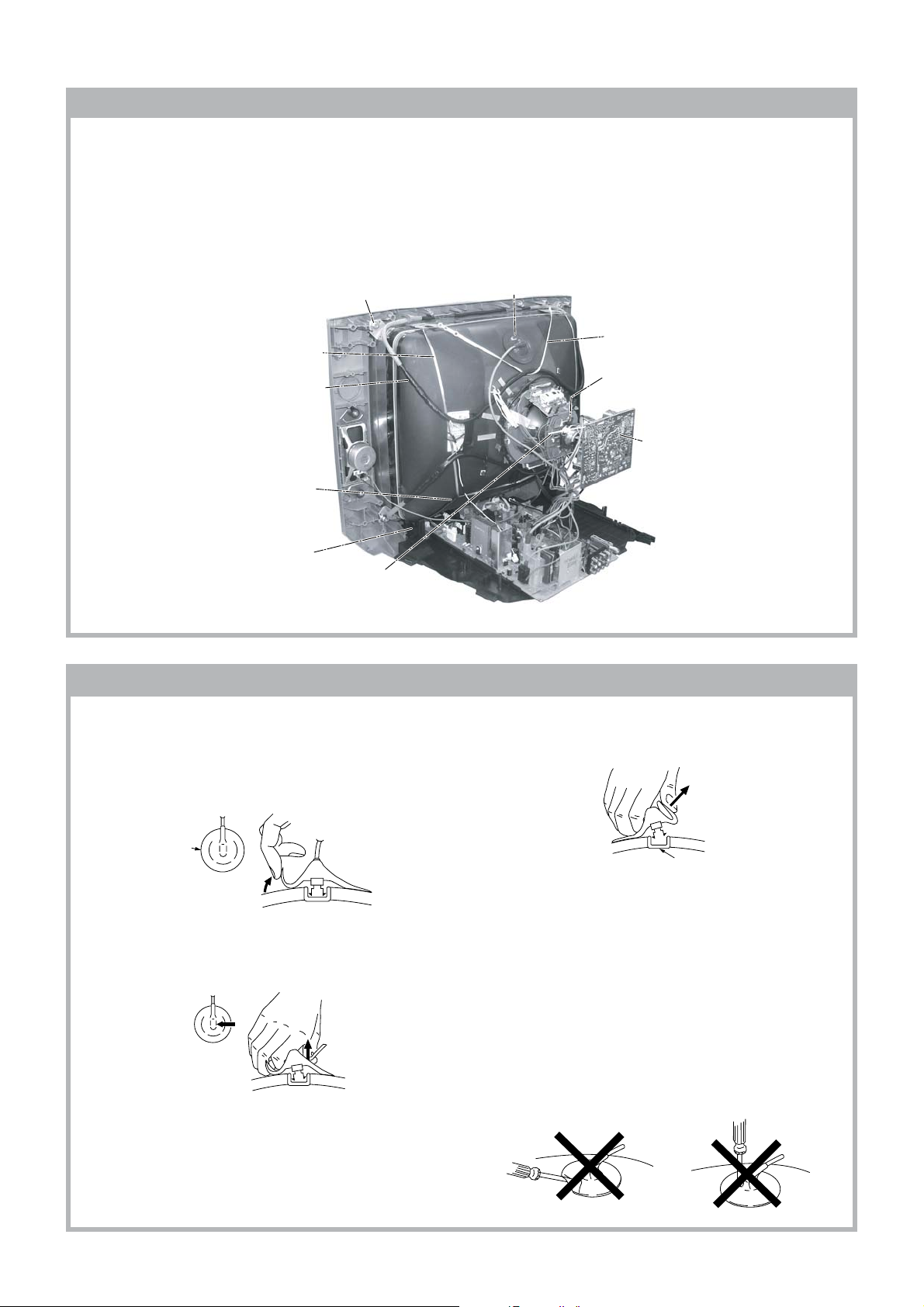
SECTION 2
WIRE DRESSING
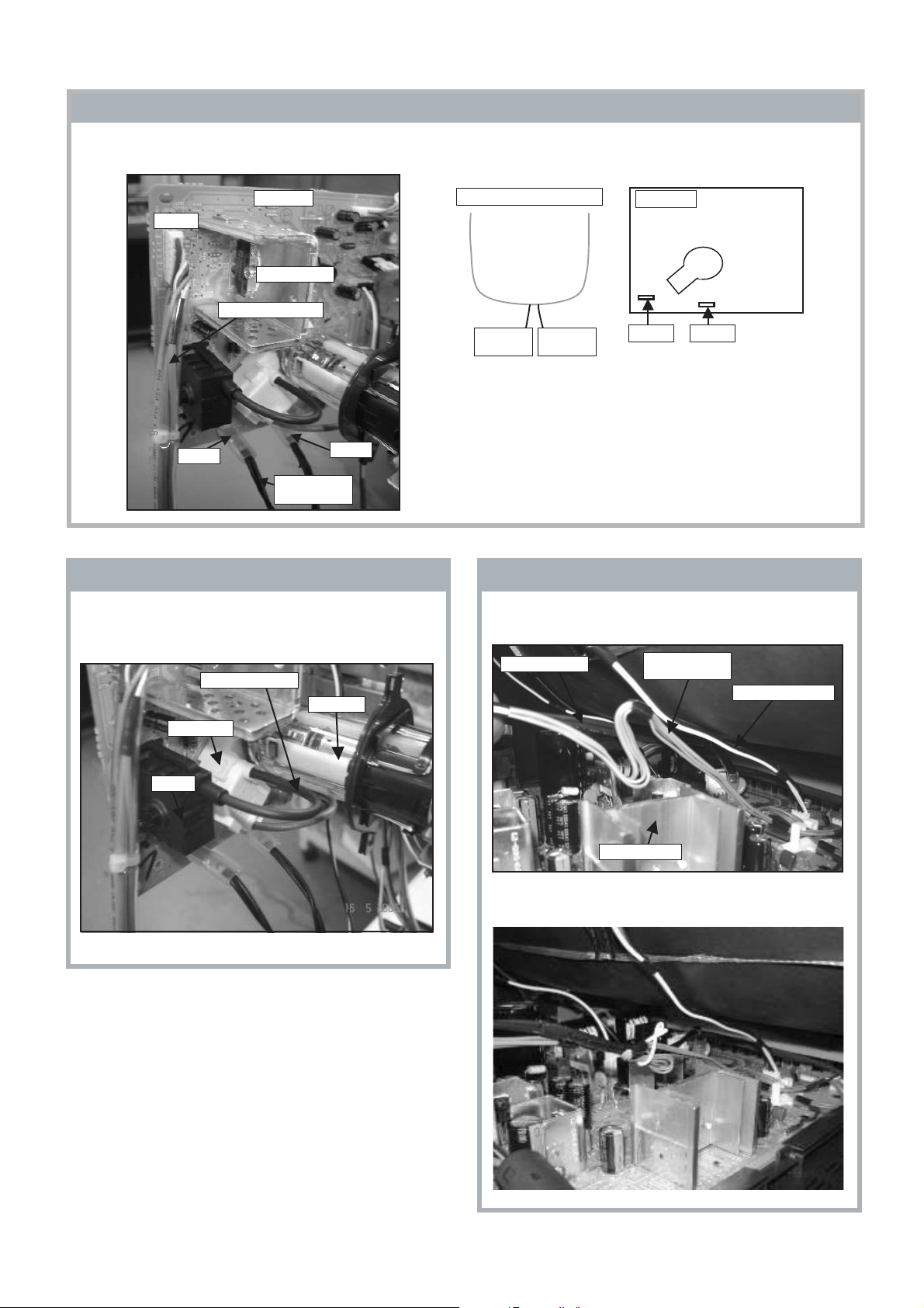
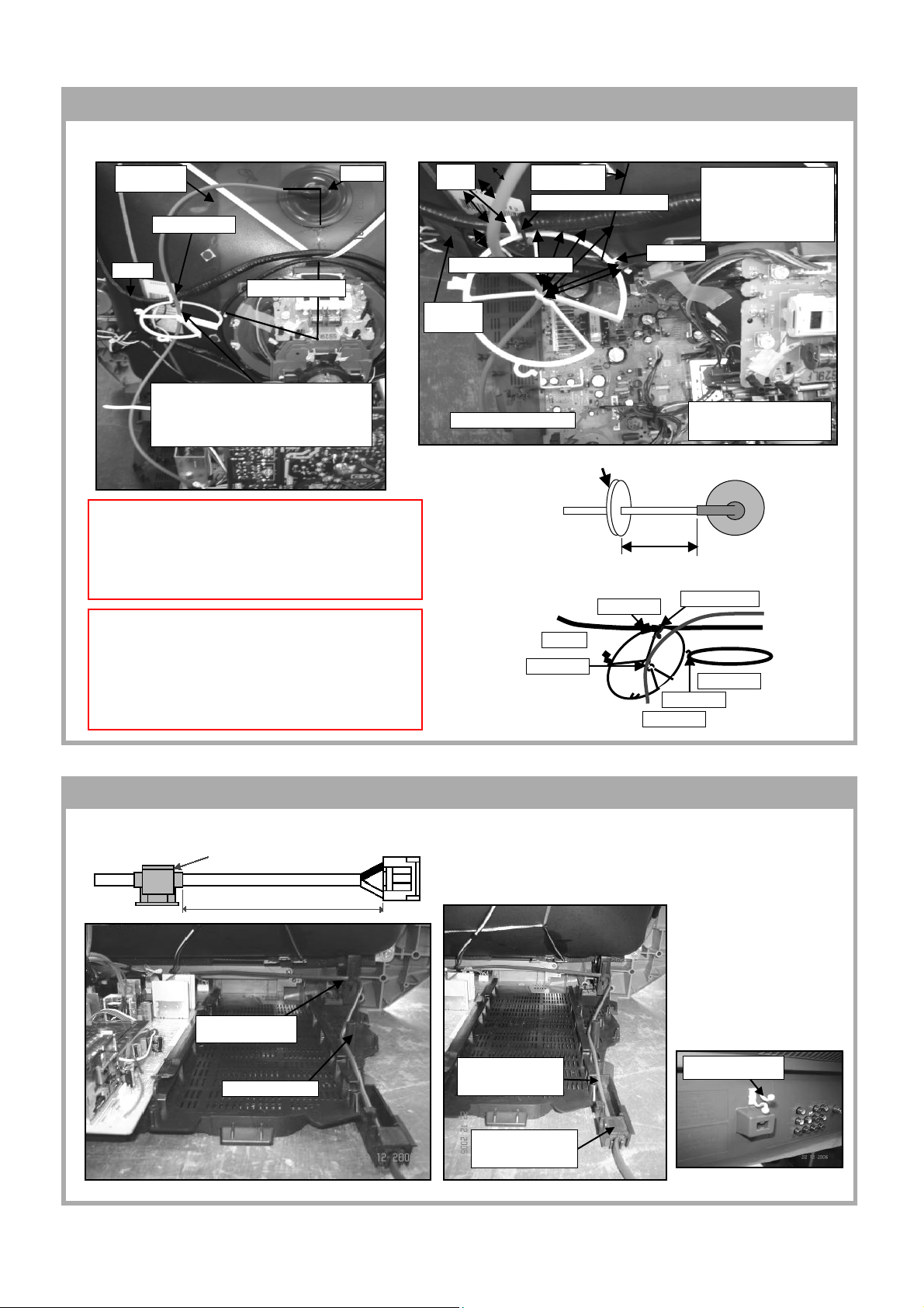
2-1. Lead Assy, Jumper Wire Dressing at A board
W082
P/N 1-923-512-11
W016
Keep Lead Assy, Jumpers
away from R121
W077
Dress both Lead Assy, Jumpers
along edge of shield case
P/N 1-910-026-28
Conn Assy,
5P YUV
CAUTION :
1. Do not ov erpull the wires during dressing
--> avoid disconnection of wires.
2. Make sure wires are kept away from
sharp edges, heatsinks & other
high-temperature parts.
2-2. Lead Assy, Jumper Wire Dressing at A board
(only for Audio 6+6 Non DSP models)
L2601
A002
W075
C211
Dress Lead Assy,
Jumper around C249
P/N 1-910-036-25
Dress Lead Assy, Jumper in
between C211 and L2601
UL Tube
A003
Dress between
T501
C514
W084
W065
No. Part No. Description Block Remark
1 1-910-026-28 Lead Assy, Jumper A(Var)
W077-W065(0)
2 1-923-512-11 WIRE UL1007 AWG24 150MM ORG A(Com) W082-W010(1)
CN905
W010
C903
Dress Lead Assy, Jumper far
away from C514 and T501
Dress both Lead
Assy, Jumpers
around CN905, C903
and below Conn
Assy, 5P YUV
W016-W084(1)
No. Part No. Description Block Remark
2 1-910-036-25 Lead Assy, Jumper A(Var) W075-W085(1)
A003 and A002
W085
2-3. Wire Dressing at A and H2 board
i) Insert and dress Conn Assy, 4P into hook. ii) Insert Conn Assy, 5P into CN4105.
Make sure AC Power Cord is behind Lead Assy,
Speaker at CN4106.
AC Power Cord is behind
Lear Assy, Speaker
Conn Assy, 4P
CN4110
1
CN2105
Conn Assy, 7P
Insert Conn Assy,
4P into hook
CN4113
CN3102
Lead Assy, Speaker
CN4105
2
CN4106
Conn Assy, 5P
– 7 –
TVSR:
Connector assy must be kept away
from primary area(10mm minimum).
KV-SZ252M50/M61/M81/N50/N60
RM-GA002
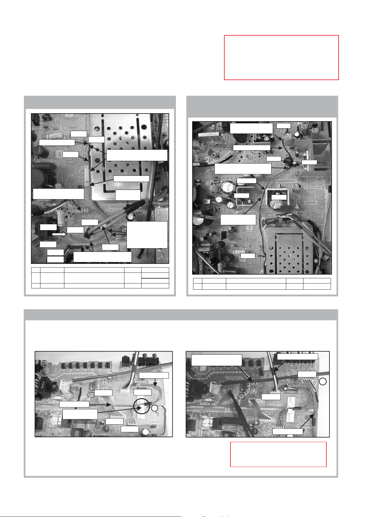
2-4. Dressing of Conn Assy, 4P VH
Dress Conn Assy, 4P VH into hook as shown.
CN4102
Insert Connector Assy,
4P VH into holder
CN6101
2-5. Dressing of Conn Assy, 5P YUV
Dress Conn Assy, 5P YUV around shield case.
Use pin, wires A019 and A017 to dress Conn Assy,
5P YUV as shown.
Pin, wire A019
CN007
Make sure the UL tape is positioned at
the sharp edge of shield case to prevent
wire from being scratched
Dress Conn Assy, 5P YUV
around shield case
CN9201
Keep wires away
from R121
CN905
Pin, wire A017
Conn Assy, 5P YUV
2-6. Dressing of Conn Assy, 4P VM and
Connector Assy, 5P Front In
Dress Conn Assy, 4P VM behind Conn Assy, 5P Front In
as shown.
Conn Assy, 5P Front In is used to prevent Conn Assy,
4P VM from bending towards T504, R579 and R5032
(high temperature parts).
Dress Conn Assy, 4P VM behind
Conn Assy, 5P Front In
Deflection area
T504
Conn Assy, 4P VM
R5032
CN003
R579
CAUTION:
Keep Conn Assy, 5P Front In away from deflection area
(T504, R5032, etc.) when dressing.
Lead Assy, Earth is
above Conn Assy, 5P
CN9201
Conn Assy, 5P
Front In
2-7. Installation and Dressing of Earth Assy
Coating
i) Earth Assy, Coating is installed as shown.
Right side Left side
– 8 –
2-8. Installation and Dressing of Earth Assy Coating
ii) Insert the 2 Earth Assy, Coating wires to CN705 &
CN707 as shown. Insert Conn Assy, 7P RGB into CN701.
KV-SZ252M50/M61/M81/N50/N60
RM-GA002
CV board
CN701
Heatsink A751
Conn Assy, 7P RGB
CN707
Coating wires
CN705
Earth Assy,
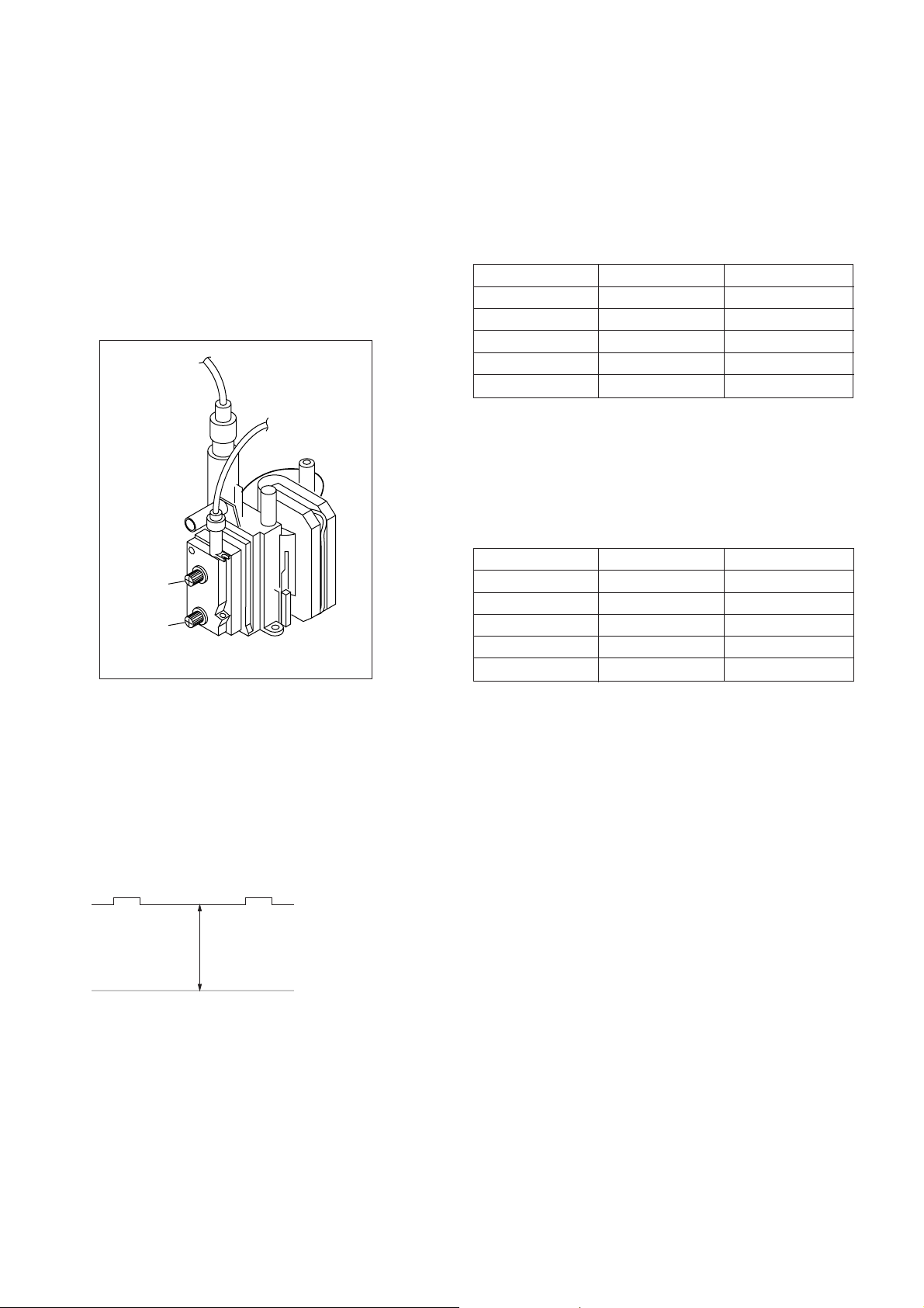
2-9. Insertion of Lead Assy, H Static
Insert Lead Assy, H Static into CRT socket and RV750 as
shown. Make sure the wire is naturally curved, to avoid
touching CRT neck.
Lead Assy, H static
CRT neck
CRT socket
Earth Assy, Coating dressing
BLK+BLK
to CN705
BLK+BLK
to CN707
CV board
CN707 CN705
2-10. Dressing of Conn Assy, 5P Front In
Make a 'S' shaped loop on Conn Assy, 5P Front In
as shown. Keep wires away from heatsink A010.
Lead Assy, Earth
Conn Assy, 5P
Front In
Lead Assy, Speaker
RV750
Heatsink A010
Next, Conn Assy, 5P Front In is dressed together with
Lead Assy,Earth using purse lock Ø 5. Refer to next page.
– 9 –
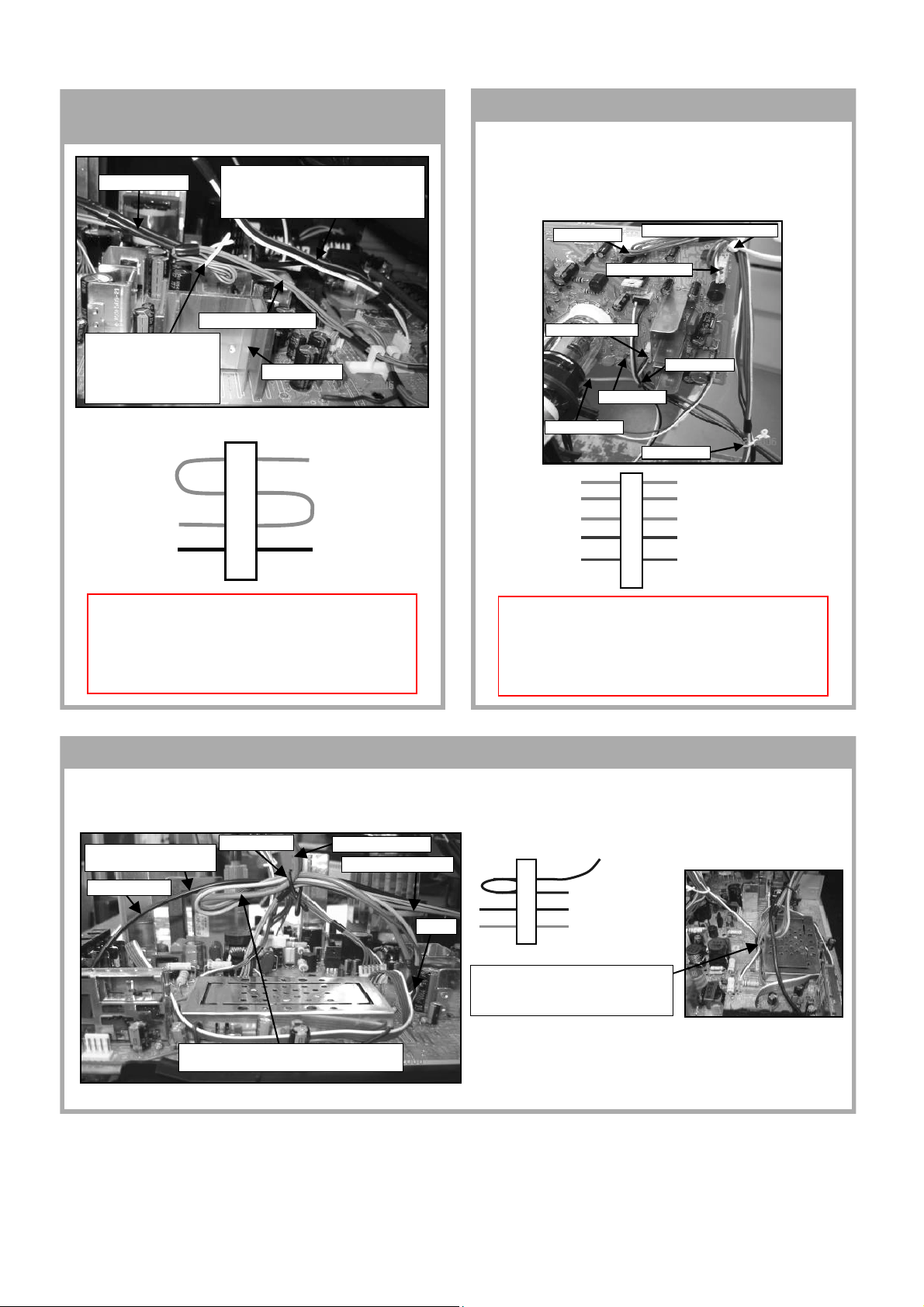
KV-SZ252M50/M61/M81/N50/N60
RM-GA002
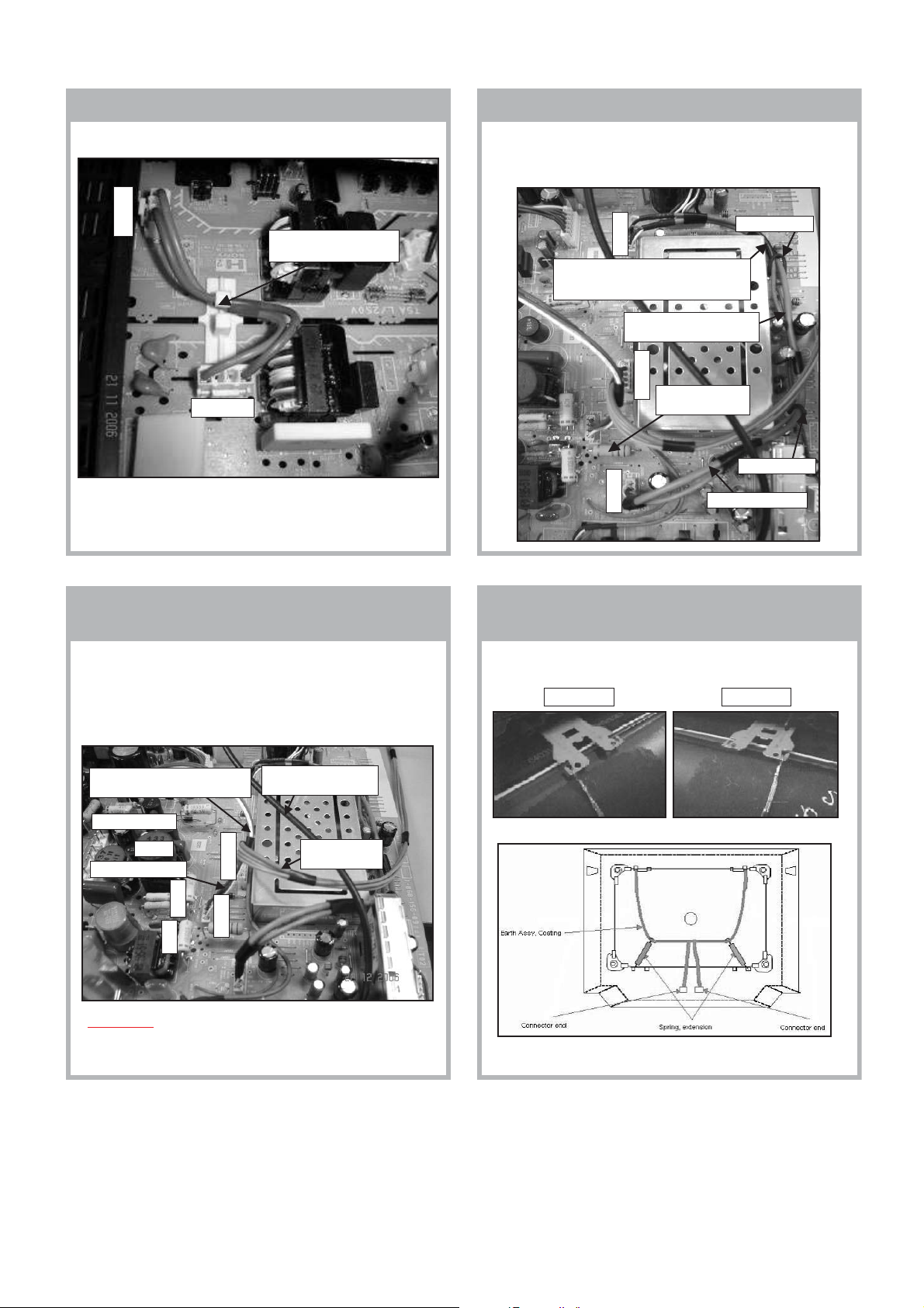
2-11. Dress Lead Assy, Earth and Conn Assy,
5P In with purse lock
Lead Assy, Earth
Make a 'S' shaped loop on
Conn Assy, 5P Front In
and dress together with
Lead Assy, Earth using
purse lock Ø 5
Note: Dress while chassis is halfway docked into beznet.
together with purse lock. Keep Lead Assy,
Conn Assy, 5P Front In
Ø
5
Lead Assy, Speaker is not dressed
Speaker away from heatsink A010 by
dressing it close to the CRT
Heatsink A010
Conn Assy,
Purse lock Ø 5
5P Front In
Lead Assy, Earth
2-12. CV Board Connector Assy Wire Dressing
i) Dress Conn Assy, 6P and Conn Assy, 4P VM using tie,
cable at alignment hole 'B' on CV board as shown.
ii) Dress Conn Assy, 4P 200V; Conn Assy, 6P; Conn Assy,
4P VM; Lead Assy, G2 and Lead Assy, Focus with purse
lock Ø 5.
Conn Assy, 6P
Conn Assy, 4P 200V
Lead Assy, Focus
Tie, cable at alignment hole 'B'
Conn Assy, 4P VM
Pin, wire A707
Lead Assy, G2
Purse lock Ø 5
Purse lock Ø 5
Conn Assy, 4P VM
Conn Assy, 4P 200V
Conn Assy, 6P
Lead Assy, Focus
Lead Assy, G2
CAUTION:
Prevent tie, cable from touching rear cover or any
enclosures by turning them away from it --> avoid
rattle sound. Also prevent tie, cable's end from
touching solder side of board.
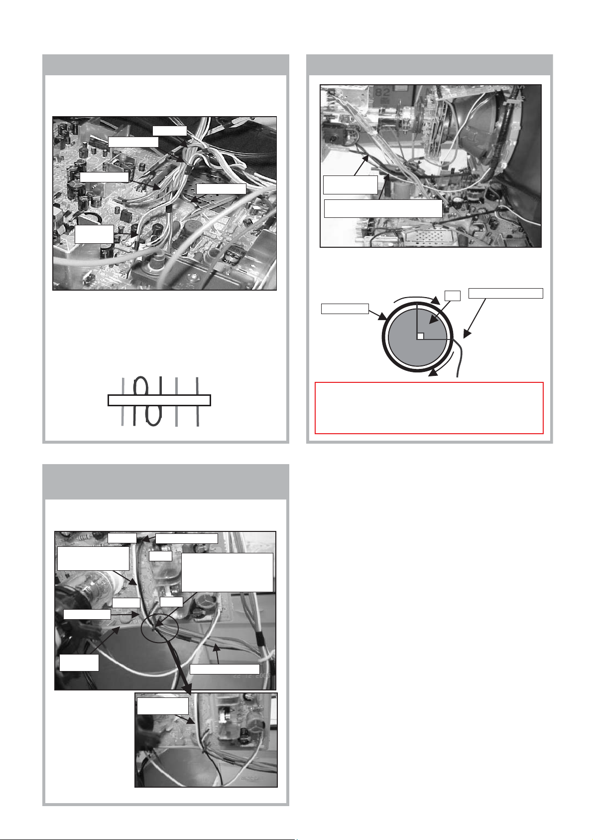
2-13. Connector Assy Wire Dressing
i) Dress Conn Assy, 7P RGB; Conn Assy, 5P Front In and
Lead Assy, Earth using purse lock Ø 9. Keep wires away from
heatsinks and high-temperature parts.
Lead Assy, Earth is behind
Conn Assy, 7P RGB
Lead Assy, Earth
Make loop of Conn Assy, 7P RGB as large as
possible when dressing with purse lock
Purse lock Ø 9
Conn Assy, 7P RGB
Conn Assy, 5P Front In
CN004
CAUTION:
Prevent tie, cable from touching rear cover or any
enclosures by turning them away from it --> avoid
rattle sound. Also prevent tie, cable's end from
touching solder side of board.
Conn Assy, 7P RGB
Lead Assy, Earth
Conn Assy, 5P Front In
Purse lock Ø 9
Keep Conn Assy, 5P Front In wire in an upward
path from CN9201 to where it is dressed with
purse lock Ø 9. This is to keep it away from
deflection area.
– 10 –
KV-SZ252M50/M61/M81/N50/N60
RM-GA002
2-14. Connector Assy Wire Dressing
Dress DY Connector; Conn Assy, 4P 200V;
Conn Assy 4P VM and Conn Assy, 6P using purse lock
Ø 9 as shown.
DY Conn
Purse lock Ø 9
Conn Assy, 6P
Conn Assy, 4P
Conn Assy,
4P 200V
Note: Make sure DY connector is inserted securely.
--> prevent it from coming out.
2-15. Overall View of Rotation Coil Conn Dressing
Earth Assy,
Coating wires
Rotation coil conn is dressed outside
and below Earth Assy, Coating wires.
Install Rotation Coil as shown.
1) Coil positioned in clockwise direction.
2) Wire is at 3 o'clock position.
Wire from Roation Coil
DY
Rotation Coil
DY Connector
Conn Assy,
4P VM
Purse lock Ø 9
Conn Assy,
4P 200V
Conn Assy, 6P
2-16. Overall View of Lead Assy, G2; Lead Assy,
Focus and Rotation Coil Conn Dressing
Avoid any stress on Lead Assy, G2; Lead Assy, Focus and
terminal at W7001.
CN1802
Keep wire away
from R781 and
heatsinks A713, A715.
W7001
Lead Assy, G2
Lead Assy,
Focus
Rotation Coil Conn
A715
connector together with Lead
Assy, G2; Lead Assy Focus
and Conn Assy, 4P 200V
A713
Conn Assy, 4P 200V
Dress Rotation Coil
using pin, wire A707
CAUTION:
Prevent wires from touching rear cover or any
enclosures by turning them away from it--> avoid rattle
sound.
Keep wire away
from R781
– 11 –
KV-SZ252M50/M61/M81/N50/N60
RM-GA002
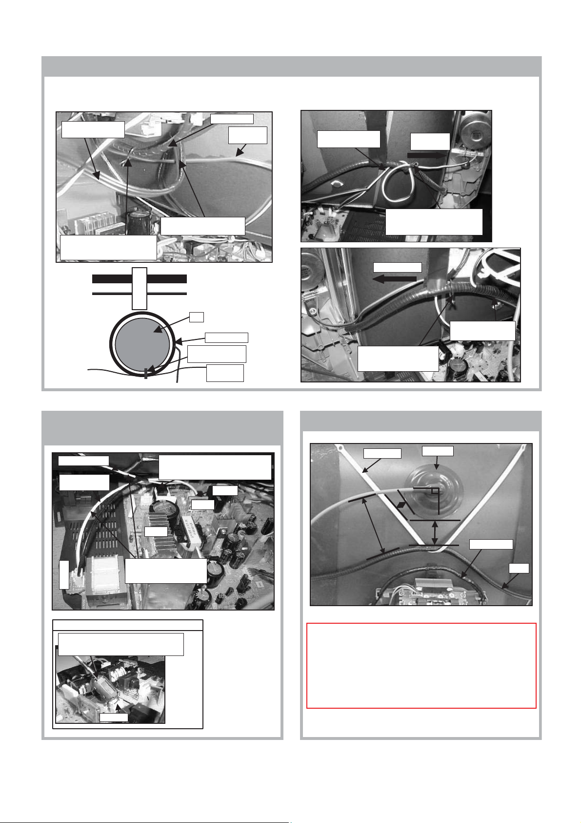
2-17. Dress Lead Assy, Speaker to Rotation Coil using Purse Lock Ø 9
Dress Lead Assy, Speaker to center position of Rotation Coil using purse lock Ø 9 as shown. Make sure Earth
Assy, Coating wire is above Lead Assy, Speaker. This is to keep Lead Assy, Speaker away from Deflection Yoke.
Earth Assy, Coating
wire
Dress Lead Assy, Speaker to
center position of Rotation Coil
using purse lock Ø 9
Purse lock Ø 9
Rotation coil
Lead Assy,
Earth Assy, Coating wire is
above Lead Assy, Speaker
Rotation Coil
Lead Assy, Speaker
(RED+BLK)
DY
Rotation Coil
Attach purse lock Ø 9
here
Lead Assy,
Speaker
Speaker
Lead Assy, Speaker
goes behind DGC
Dress Lead Assy, Speaker
directly on to DGC using
Pull wire to
the right
Loop Lead Assy, Speaker and
dress directly on to DGC using
purse lock
Pull wire to left
purse lock Ø 9
Ø 9
Lead Assy, Speaker
goes behind DGC
2-18. Dressing of PF Board Conn Assy
(for models with PF board only)
DGC Connector
Connector Assy,
3P VH
heatsinks A007, D604 and
CN6620
Apply to all SZ252 Narrow 220V CISPR models ONLY
Clamp the ferrite core at the end of the DGC
wire as shown. Position it directly above DGC
Connector's housing
DGC Connector is below Conn Assy,
3P VH to keep Conn Assy, 3P VH
away from Heatsink A007 and D604
D604
A007
Keep wires away from
conductive parts
CN605
2-19. Cap Assy, High Voltage Installation
DGC Band
>5mm
Keep distance of
1mm/kV
TVSR Requirement:
1. Keep HV cable away from conductive parts
(distance of 1mm/kV).
2. Keep spacing between edge of anode cap
& conductive parts (distance of 0.5mm/kV).
3. Keep spacing between edge of anode cap &
non-conductive parts (distance of at least 5mm or more).
HV Cap
90º
Keep distance of
0.5mm/kV
Rotation coil
DGC
Housing
– 12 –
2-20. HV Cap Assy Wire Dressing
Dress Cap Assy, High Voltage with Holder, HV Cable combi as shown.
KV-SZ252M50/M61/M81/N50/N60
RM-GA002
CRT's carbon
area
purse lock Ø 9.
DGC
10 o'clock position
Dress Holder, HV Cable Combi to Cap Assy,
High Voltage and attach side hook to rotation
coil at 10 o'clock position. Then, attach large
hook to DGC and dress with
purse lock
Ø
9.
HV cap
90º
CAUTION: 1) Make sure the specified position is
being followed.
2) Position the Cap Assy, High Voltage in
the inner ring of the Holder, HV cable
combi (see diagram).
TVSR requirement:
1. Spacing between HV cable and other conductive
part's surface is 1mm/kV or more.
2. Spacing between HV cable's and enclosure with
ventilation or the edge where terminal bracket and
rear cover meet: 10mm or more.
Large
hook
Min. distance = 1mm/kV
P-P taping
of DGC
Min. distance = 1mm/kV
CRT's carbon
area
Dress using Purse lock Ø 9
Holder, HV cable combi
250 ± 5 mm
Large hook
DGC
Inner Ring
Dress Holder, HV Cable
Combi to the right of P-P
taping of DGC. Dress
purse lock
of large hook on Holder,
HV Cable Combi.
Side hook
Keep distance of HV cable
from other wires, conductive
parts and CRT's carbon area
Purse lock Ø 9
Rotation coil
Side hook
Top view
Ø
9 to the right
2-21. AC Power Cord Wire Dressing
Install AC cord holder to AC power cord at specified position as shown.
AC Cord Holder
290 ± 5mm 630 ± 5mm
Hook AC cord into
CRT support's hook
Make sure AC cord is
straight between
Dress behind boss
boss and holder
Attach AC cord onto
holder and insert to
bottom cover
Attach Purse Lock (S)
Ø 8 in to rear cover
– 13 –
KV-SZ252M50/M61/M81/N50/N60
RM-GA002
SECTION 3
SET-UP ADJUSTMENTS
The following adjustments should be made when a complete
realignment is required or a new picture tube is installed.
Perform the adjustments in order as follows :
1. Beam Landing
2. Convergence
3. Focus
The controls and switch should be set as follows unless
otherwise noted:
4. G2(SCREEN)
5. White Balance
Picture Control....................................."NORMAL"
Brightness Control..............................."NORMAL"
Note : Test Equipment Required.
1. Pattern Generator 5. Oscilloscope
2. Degausser 6. Landing Checker
3. DC Power Supply 7. XCV Adjuster
4. Digital Multimeter
......................................................................................................................................................................................................................
Preparation :
•Feed in the white pattern signal.
6. Then move the DY forward and adjust so that the entire
screen becomes green.
• Before starting, degauss the entire screen with the
degausser.
• In order to reduce the geomagnetism on the set's picture
tube, face it east or west.
3-1. BEAM LANDING ADJUSTMENT
1. Input a raster signal with the pattern generator.
2. Loose the deflection yoke(DY) mounting screw, and set
the purity control to the center as shown below:-
Purity control
3. Position Neck Assy as shown below:-
Neck assy
Align the edge of
the neck assy with
the edge of the G2 grid.
G2G1 G3
4. Set the raster signal of the pattern generator to green.
5. Move the DY backward and adjust the purity control so
that green is in the center and blue and red are at the
sides evenly.
7. Now switch over raster signal to red then blue and
confirm the condition.
8. When the position of the DY is determined, tighten it with
the DY mounting screw.
9. If the beam does not land correctly in all the corners of
the screen, use magnet disc to correct it.
Purity control
corrects this area.
b
c
Deflection yoke positioning
corrects these areas.
a
a
d
d
Disc magnets or rotatable
disc magnets correct these
areas (a-d).
b
c
Red
Blue
Green
– 14 –
KV-SZ252M50/M61/M81/N50/N60
RM-GA002
3-2. CONVERGENCE ADJUSTMENT
Preparation:
• Before starting, perform FOCUS adjustment.
• Picture Mode "CUSTOM"
• Receive dot/cross hatch pattern.
a) Vertical Static Convergence
Center dot
R G B
R
G
B
4 pole magnet
RV750
H. STAT
b) Horizontal Static Convergence
If the blue dots does not converge with the red and
green dots, use the 6 pole magnet to adjust in
the manner described below:-
RG B R G B R GB
RB
G
RG
6 Pole
Magnet
GB
RB
RV1800
G2 (SCREEN)
1. (Moving vertically), adjust the 4 pole magnet to
converge red, green and blue dots in the center of
the screen.
2. Tilt the 4 pole magnet and adjust static convergence
to open or close the 4 pole magnet.
3. When the 4 pole magnet is moved in the direction of
arrow A and B, the red, green and blue dots moves
as shown below:-
A
B B
A
B
G
R
B
B
G
R
Moved RV750 (H.STAT)
6 Pole Magnet
Purity
DY pocket
4 pole Magnet
4 Pole
Magnet
c) Y Separation axis correction magnet adjustment.
1. Receive cross hatch signal.
2. Set Picture to "MINIMUM", Brightness to "STANDARD".
3. Adjust the Y separation axis correction magnet on
the Neck Assembly so that the horizontal lines at
the top and bottom of the screen are straight.
Neck assy Neck assy
RedBlue
RedBlue
RGGRB
B
VM board VM board
– 15 –
KV-SZ252M50/M61/M81/N50/N60
RM-GA002
d) Convergence Rough Adjustment
Preparation:
• Before starting this adjustment, adjust the
horizontal and vertical static convergence.
Input cross hatch pattern.
i) TLH
Adjust the horizontal convergence of red and blue
dots by inserting TLH Correction Plate to the DY
pocket(left or right).
ii) YCH
Adjust YCH to balance Y axis.
iii) TLV
Adjust the vertical convergence of red and blue dots.
iv) XCV
Adjust XCV to balance X-axis
B
R
TLH
(VR2)
YCH
RB
YCH
B
R
ON DY :
(VR1)
TLV1 (no need to adjust)
TLV
DY pocket
b1
a1
c1
d1
R
B
a1~d1: Piece A(90), Convergence Correct
or
Permaloy Assy Correction
XCV
(VR3)
TLV2
(XCV)
DY pocket
TLH Plate
e) Screen Corner Convergence
Affix a Piece A(90), Convergence Correct/Permaloy Assy
Correction to the misconverged areas.
ba
a-d : screen-corner
misconvergence
cd
– 16 –
KV-SZ252M50/M61/M81/N50/N60
RM-GA002
3-3. FOCUS ADJUSTMENT
FOCUS adjustment should be completed before W/B
adjustment.
1. Receive digital monoscope pattern.
2. Set Picture Mode to "VIVID".
3. Adjust focus VR to obtain a just focus at the
center of the screen.
4. Change the receiving signal to white pattern
and blue back.
5. Confirm magenta ring is not noticeable. In case
magenta ring is obvious, then adjust FOCUS VR
to balance magenta ring and FOCUS.
3-5. SUB BRIGHT ADJUSTMENT
1. Set TV to RF mode.
2. Input PAL monoscope to RF mode (OTHER model) and
NTSC monoscope (NTSC model).
3. Set Brightness to 50% and Picture to "MINIMUM" in
"CUSTOM" mode.
4. Select WHBL 010 "SBRT" with 1 and 4 button and
adjust its data using 3 and 6 button so that the Cut Off
level and slightly glimmer is as the specification below:-
TV size Cut Off Slightly Glimmer
25" 10 IRE 20 IRE + 2 steps
29" 10 IRE 20 IRE + 2 steps
34" 10 IRE 20 IRE + 2 steps
28" 10 IRE 20 IRE
32" 10 IRE 20 IRE
5. Write into the memory by pressing [MUTING] t -.
6. Copy the adjusted data WHBL 010 “SBRT” to Video
mode.
7. Once adjustment is completed in RF and Video mode,
carry out adjustment in DVD mode. Repeat step 2 to 3.
Select WHBL 010 “SBRT” and adjust its data as the
specification below:-
Focus
Screen
FLYBA CK TRANSFORMER (T503)
3-4. G2 (SCREEN) ADJUSTMENTS
1. Set the following condition:
- Picture and Brightness to "STANDARD".
- TV to Video mode.
- WHBL 013 "RGBB" to 01.
2. Connect R,G,B of the CV board cathode to
oscilloscope.
3. Adjust Brightness to obtain the cathode value
to the value stated below.
Cathode setting voltage:
175 V ± 2 (VDC)
TV size Cut Off Slightly Glimmer
25" 10 IRE 20 IRE + 2 steps
29" 10 IRE 20 IRE
34" 10 IRE 20 IRE + 2 steps
28" 10 IRE 20 IRE
32" 10 IRE 20 IRE
3-6. WHITE BALANCE ADJUSTMENT
1. Set to Service Mode.
2. Input white raster signal using signal generator.
3. Set the following condition:
Picture "VIVID", PICT 006 "WTS" to 00.
4. At Highlight condition, select WHBL 003 "GDRV"
and 002 "RDRV" with 1 and 4 button of the
remote commander then adjust the data with
3 and 6 button.
5. At Cutoff, select WHBL 000 "BKOR" and 001 "BKOG"
and adjust the data.
6. Perform adjustment at Hightlight and Cutoff condition
until it reaches its target.
7. Write data into memory by pressing [MUTING]t-.
8. Finally set PICT 006 "WTS" back to its original data.
4. Adjust SCREEN VR on the FBT until the scanning line
disappears.
5. Finally set WHBL 16 "RGBB" back to 00.
– 17 –
KV-SZ252M50/M61/M81/N50/N60
RM-GA002
SECTION 4
CIRCUIT ADJUSTMENTS
4-1. ADJUSTMENT WITH COMMANDER
Service adjustments to this model can be performed using the supplied remote commander RM-GA002.
a. ENTERING SERVICE MODE
With the unit on standby
t [DISPLAY] t 5 t [VOL $+% ] t [POWER]
This operation sequence puts the unit into service mode.
This screen display is:
Category in decimal Item name in decimal NG Command Frequency Video Input Name
GEOM 006 EWPW 031 x SERVICE 60 S VIDEO 1
Item no. Service data NVM Service Field Channel no./
Release ID Version in binary for factory Color System (decimal)
NT01 3.50M 0001 1111 FF FF NTSC3 65553
Status SID,
Lock, SL
:not locked
(no signal) Status Status BC, Status Status S/N Status Status Display
:locked VW, IVWF HBC BCF LEVEL (0-7) GL Area
111 11 11 1 7 11 ZZ xy 1 1 000000 000000
S: for Sony
A: for AIWA
L: BX1L Full
B: BX1L Basic
D: DVD Combo
N T : Taiwan/Korea/Philippines
G A : General Area
01 : Serial no. of the M / P release for each destination
Software Service data Reserved Power On Time
Status
PTW
ZZ : DCXO Flash Value
xy : Value of x : Value of y
0 - unknown 0 - Mono
1 - BTSC 1 - Stereo
2 - A2 2 - Bilingual
3 - NICAM 4 - SAP/Single
4 - KOREAN
5 - Japan
6 - AV Stereo
b. METHOD OF CANCELLATION FROM SERVICE MODE
Set the standby condition (Press [POWER] button on the commander), then press [POWER] button again, hereupon it becomes
TV mode.
c. METHOD OF WRITE INTO MEMORY
1. Set to Service Mode.
2. Press 1 (UP) and 4 (DOWN), to select the adjustment item.
3. Change item by pressing
3, 6.
4. Press [MUTING] button to indicate WRITE on the screen.
5. Press
- button to write into memory.
1, 4 Select the adjustment item.
r
3, 6 Raise/lower the data value.
r
[MUTING] Writes.
r
- Executes the writing.
d. MEMORY WRITE CONFIRMATION METHOD
1. After adjustment, pull out the plug from AC outlet, and then plug into AC outlet again.
2. Turn the power switch ON and set to Service Mode.
3. Call the adjusted items again to confirm adjustments were made.
– 18 –
e. OTHER FUNCTION VIA REMOTE COMMANDER
7, - All the data becomes the values in memory.
8, - All user control goes to the standard state.
[Display], - Service data initialization (Be sure not to use usually.)
2, 5 Select Device or Category (Up, Down)
4-2. ADJUSTMENT METHOD
Item Number 000 HPOS
This explanation uses H POSITION as an example.
1. Select "000 HPOS" with the 1 and 4 buttons, or 2 and 5.
2. Raise/lower the data with the
3. Select the optimum state. (The standard is IF for PAL reception.)
4. Write with the [MUTING] button. (The display changes to WRITE.)
5. Execute the writing with the
SERVICE.)
Example on screen display :-
3 and 6 buttons.
- button. (The WRITE display will be changed to red color while excuting, and back to
KV-SZ252M50/M61/M81/N50/N60
RM-GA002
GEOM
SUS01
GEOM
SUS01
GEOM
SUS01
Use the same method for all Items. Use
then execute the write with
-.
HPOS
000
3.50M FF FF
HPOS
000
3.50M FF FF
HPOS
000
3.50M FF FF
1 and 4 to select the adjustment item, use 3 and 6 to adjust, write with [MUTING],
031
SERVICE
1111
0001
031
WRITE
1111
0001
Write with [MUTING]
031
WRITE
1111
0001
Write executed with -
50
NTSC3 65553
50
NTSC3 65553
50
NTSC3 65553
GREEN
Adjusted with 3
and 6 buttons.
GREEN
RED
The WRITE display
then the display
returns to green
SERVICE.
Note : 1. In [WRITE], the data for all items are written into memory together.
2. For adjustment items that have different standard data between 50Hz or 60Hz, be sure to use the respective input
signal after adjustment.
– 19 –
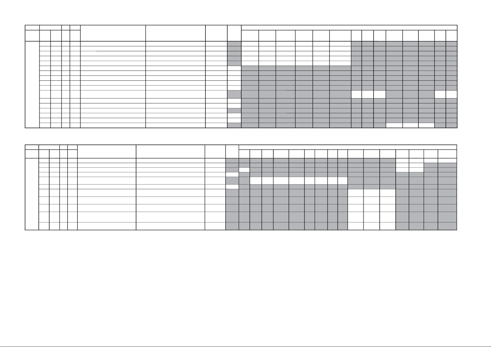
Adjustment Item Table
JVTytilanoitcnuF.tinIegnaRnoitcnuFemaNeciveDnommoC)deliateD(eulaVlaitinI
yrogetaC.oNemaNceDceD 05)3:4(06)3:4(05w)3:4(06w)3:4(
MOEG000SOPH130360)SH(tfihSlatnoziroHrossecorP-VT
62630373
100RAPH130360margolellaraPlatnoziroH
34442454
200WOBH130360woBlatnoziroH
03426282
300NILV130360ytiraeniLlacitreV
93939393
400RCSV130360llorcSlacitreV
13131313
500ZISH130360)WE(htdiWWE
24146474
600WPWE130360)WP(htdiW/alobaraPWE
54749453
700POCU710360alobaraPrenroCreppUWE
04839375
800POCL710360alobaraPrenroCrewoLWE
54748551
900ZTWE130360muizeparTWE
72718113
010PLSV130360)SV(epolSlacitreV
13131313
110ZISV510360edutilpmAlacitreV
12128191
210ROCS410360)CS(noitcerroC-S
73737373
310SOPV130360)HSV(tfihSlacitreV
84940444
410MOZV130360)ZV(mooZlacitreV
00000000
510LBH000100edoMgniknalBBGR
10101010
610FBW700510)FBW(gniknalBediWfognimiT
01300130
710RBW700510)RBW(gniknalBediWfognimiT
11011101
810LBS000100gniknalBecivreS00
910YPOC000100aeraMVNzH06/05llaotatadOEGehtypoCX
NOTE
a) In the initial value (detailed) column, the data after the slash mark ("/") refers to NTSC model data.
No ("/") means data is common for Multi and NTSC model.
b) Item remarked "*", please refer page 32 for the data.
c)
shaded items are no data.
d) Standard data listed on the Adjustment Item Tab le are reference values, therefore it may be different for each model and for each mode.
e) Note for the Different Data those are the standard data values written on the microprocessor. Therefore, the data values of the models are stored respectively in the memory.
In the case of a device replacement, adjustment by rewriting the data value is necessary for some items.
f) Multi ver8.21, NTSC ver8.21N.
KV-SZ252M50/M61/M81/N50/N60
RM-GA002
– 20 –
– 21 –
JVTytilanoitcnuF.tinIegnaRnoitcnuFetoN&elbaTemaNeciveDnommoC )deliateD(eulaVlaitinI
yrogetaC.oNemaNceDceD
pmeTloC
LOOC(
)rehto
pmeTloC
MRAW(
)rehto
pmeTloC
LARTUEN(
)rehto
pmeTloC
)VUYLOOC(
pmeTloC
MRAW(
)VUY
pmeTloC
LARTUEN(
)VUY
VUYlap05
)N(
lap05
)oediV(
0edomciP
diviV/
1edomciP
dtS/
2edomciP
motsuC/
VToediV
LBHW000ROKB130360)10=BFO(BtesffO,)00=BFO(RtesffOleveLkcalB )srehtO/BGR/VU(*)lamroN/WOL/HGIH(pmetlocrossecorP-VT
131313131313
100GOKB130360GtesffOleveLkcalB )srehtO/BGR/VU(*)lamroN/WOL/HGIH(pmetloc
020202020202
200VRDR730360RtnioPetihW )srehtO/BGR/VU(*)lamroN/WOL/HGIH(pmetlocrossecorP-VT
737373737373
300VRDG730360GtnioPetihW )srehtO/BGR/VU(*)lamroN/WOL/HGIH(pmetloc
542473542473
400VRDB730360BtnioPetihW )srehtO/BGR/VU(*)lamroN/WOL/HGIH(pmetloc
340403340403
500GPL000100teserPniaGBGR enon00
600RGP130721)RGP(RniaGteserP enon95
700GGP130721)GGP(GniaGteserP enon95
800BGP130721)BGP(BniaGteserP enon95
900FONG000510tesffOniaGteserP enonpoolCCC01
010TRBS
130360ssenthgirB-buS nlaP*/)VT(nlaP*/)oediV(rehtO/VT(srehtO
]ylnosledomSU*[VUY/)oediV(
235333
5333
110ORBS000300)ciPtnegilletnI(tesffOssenthgirB-buS enon00
210SBC000100gnitimiLtnerruCmaeBfoecneuqeSlortnoC enon00
310BBGR000300gniknalBBGR enon
410GBLB000100tuptuOneerG&eulBfogniknalB enon00
510BFO000100eulBtesffOleveLkcalB enon10
610PBW000300)woL:3,2,lamroN:1,hgiH:0(gnitteSpmeTroloC edoMerutciP
001010
JVTytilanoitcnuF.tinIegnaRnoitcnuFetoN&elbaTemaNeciveDnommoC )deliateD(eulaVlaitinI
yrogetaC.oNemaNceDceD
VUYlap05
)VT(
lap05
)oediV(
maceS05
)VT(
maceS05
)oediV(
cstn06
)VT(
cstn06
)oediV(
VUY05VUY06/0edomciP
diviV
/1edomciP
dradnatS
/2edomciP
motsuC
VToediV
ediWVT
)3:4(
ediWoediV
)3:4(
JDAS000XAMP360360mumixaMerutciP >ediW/lamroN</)ediW/lamroN(*)oediV/VT(rossecorP-VT
84842424
100EUHS700510euH-buS oediV/VT
6011
200PHSS510360ssenprahS-buS VUY/oediV/VT
03
6243
300OHSS000700)ciPtnegilletnI(tesffOssenprahS-buS enon40
400LOCS130360roloC-buS /)oediv(maces05/)vt(maces05/)oediv(lap05/)vt(lap05
BGR06/BGR05/VUY06/VUY05/oediv06/VT06
5373921333131443
500OOCS000300)ciPtnegilletnI(tesffOroloC-buS enon20
600CIP130721;)dilavni(001>;)dilav(001~0:AG[lortnoCerutciP
])dilavni(6tiberongi;)dilav(36~0:srehtO
)ataDteseRresU=lanosreP:AG(ledoMerutciP
00117001
700LOC130721;)dilavni(001>;)dilav(001~0:AG[lortnoCroloC
])dilavni(6tiberongi;)dilav(36~0:srehtO
)ataDteseRresU=lanosreP:AG(ledoMerutciP
751405
800TRB130721;)dilavni(001>;)dilav(001~0:AG[lortnoCssenthgirB
])dilavni(6tiberongi;)dilav(36~0:srehtO
)ataDteseRresU=lanosreP:AG(ledoMerutciP
847405
900EUH130721;)dilavni(001>;)dilav(001~0:AG[lortnoCeuH
])dilavni(6tiberongi;)dilav(36~0:srehtO
)ledomSUhtiw)0-5(hE1#TNITotdneS*(
)ataDteseRresU=lanosreP:AG(ledoMerutciP
058405
010PHS130721;)dilavni(001>;)dilav(001~0:AG[lortnoCssenprahS
])dilavni(6tiberongi;)dilav(36~0:srehtO
)ataDteseRresU=lanosreP:AG(ledoMerutciP
850505
KV-SZ252M50/M61/M81/N50/N60
RM-GA002
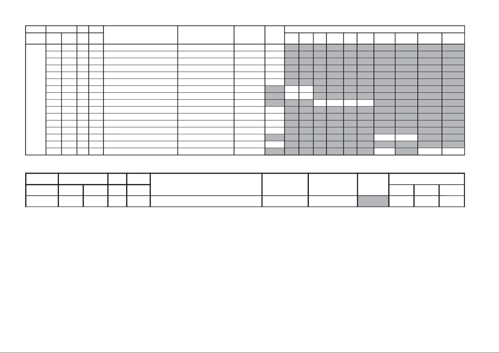
JVTytilanoitcnuF.tinIegnaRnoitcnuFetoN&elbaTemaNeciveDnommoC )deliateD(eulaVlaitinI
yrogetaC.oNemaNceDceD srehtOVUY)VT(LAP)VT(CSTN)VT(MACES)oediV(LAP)oediV(CSTN)oediV(MACESTUPNI-SMACESCSTNVT
CY000QRFP000300yaleDdnaycneuqerFretneCgnikaeP rehto/VTrossecorP-VT
00
00
100APR100300toohSrevO&erPoitaR rehto/VT
20
20
200OPR200300skaePevitageN&evitisoPfooitaR rehto/VT
20
20
300YLDY210510yaleD-Y TUPNI-S/VUY+)OEDIV/VT(*)MACES/CSTN/LAP(
** * * * * *
400TAMC000300xirtaM)ASU/napaJ(CSTNroMACES-LAP 00
500LCA100100gnitimiLroloCcitamotuA 10
600BC000100ycneuqerFretneCssapdnaBamorhC )xif0:oediV*(VThtiwylnodilav00
700OBS100300tesffOkcalBMACES 10
800ESHC100300ytivitisneStnedICSTN/LAP 20
900OLC000100retliF)lleB(ehcolCfoycneuqerFretneC 00
010PRTC000100edoMparTamorhC srehto/MACES
*
*
110TDQ000100parTamorhCdnoceS srehto/MACES
*
*
210SPB
000100eniLyaleDdnab-esaBamorhCfossapyB
srehto/CSTN
00
*
310OCF
000100nOroloCdecroF 00
410TNIT130360lortnoCtniTdnaB-esaB VT/srehto/VUY
2323
23
510VUT000100slangiSVUnolortnoCtniT 00
610CYWB000100
roloczH85.3rofedomCYtahtdiwdnaB
)CYWB(metsys
00
710BSO000100
amorhcfoeslupyektsrublanretnifohtdiW
)BSO(rotaludomed
00
810CKB000100noitisoPyektsruB
00
1000
JVTytilanoitcnuF.tinIegnaRnoitcnuFetoN&elbaTemaNeciveDnommoC)deliateD(eulaVlaitinI
yrogetaC.oNemaNceDceD 05)3:4(06)3:4(srehtOVUY)FFO_PI(VToediVtxeteleT)NO_PI(pi-VTlangisoN
CNYS000SYS000100tupnICNYSYnonoitazinorhcnyS 00
100OF000300tnatsnoCemiT1esahP )FR(langisoNrogninuTotuA/txeteleT/oediV/FFOPIVT/NOPIVT
3030100000
200DIV000100edoMtnedIoediV 06/05
0000
300LSF000100cnySlacitreVrofleveLgnicilSdecroF 00
400LSS000100rotarapeScnySleveLgnicilS 06/05
0000
500DIVS100700noitacifitnedIoediVrofnoitceleSecruoS srehtO/VUY
0000
600FROF000300ycneuqerFdleiFdecroF 30
700KVM000100gniyeKnoisiVorcaM 10
(For '*' refer to page 32)
– 22 –
KV-SZ252M50/M61/M81/N50/N60
RM-GA002
– 23 –
JVTytilanoitcnuF.tinIegnaRnoitcnuFetoN&elbaTemaNeciveDnommoC )deliateD(eulaVlaitinI
yrogetaC.oNemaNceDceD
srehtOdiviVVT
)nyD(
VT
)srehtO(
oediV
)nyD(
oediV
)srehtO(
pmeTroloC
)HGIH(
pmeTroloC
)srehtO(
roloC
)WOL(pmeT
pmeTroloC
)LAMRON(
TCIP000LDAC700510leveLevirDedohtaC 30
100AFC000300edoMretliFbmoC *
200COS200300leveLgnippilCtfoS 00
300LWP100100hctiwSgnitimiLetihWkaeP 10
400LTHW600510gnitimiLetihWkaeP 20
500MAG100100ammaG 10
600STW100300hctertSetihWdnalortnoCammaGsrehtO/eviL
10/*10/*
700RFT000100langiSecnanimuLfooitaRrefsnarTCDsrehtO/eviL
1010
800ROC300300gniroC )srehto/anyD(*)oediV/VT(
10200010
900OROC000300)ciPtnegilletnI(tesffOgniroC 10
010SKB300300hctertSkcalBsrehto/BGR20
110SAA100100hctertSkcalBehtffohctiwSotaerAkcalB 10
210KSD000100lortnoCnikScimanyD 00
310SLB000100hctertSeulB )SREHTO/HGIH(pmetloc
0000
410SLBN000100tiucriChctertSeulBnoitarepO 00
510RRN000100noitcudeRdeRnoN )LAMRON/WOL/HGIH(pmetloc
10
1010
JVTytilanoitcnuF.tinIegnaRnoitcnuFetoN&elbaTemaNeciveDnommoC)deliateD(eulaVlaitinI
yrogetaC.oNemaNceDceD VUYVToediV
WS100OVS10030084@niPISBVC/OVS/OVFIfonoitcnuFVUY/oediV/VT
301010
KV-SZ252M50/M61/M81/N50/N60
RM-GA002
– 24 –
JVTytilanoitcnuF
laitinI
egnaR
noitcnuFetoN&elbaTemaNeciveDnommoC
yrogetaC.oNemaNceDceD
FIV000DFIO630360rotaludomeDFItesffO rossecorP-VT63
100TCGA130360revo-ekaTCGA 81
200MTS000100edoMgninuThcraeS 10
300DG000100langiS1SBVCnoyaleDpuorG 00
400SCGA100300deepSCGAFI 10
500IFF000100LLPFIretliFtsaF 00
600IANL000100eulavlaitinitibANLpmAFR 00
700TANL591522leveLdlohserhTpmAFR 591
800NSNL400700dlohserhTleveLNSpmAFR 30
900DSNL200700dlohserhTporDleveLNSpmAFR 10
010XENL610360gnimiTporDNSkcehcpmAFR 03
110RTHC840721edoMresUpmAFRtesotgrPotuAretfadlohserhTlennahC 52
210OSUT000100desUrenuTynoS *
JVTytilanoitcnuF.tinIegnaRnoitcnuFetoN&elbaTemaNeciveDnommoC)deliateD(eulaVlaitinI
yrogetaC.oNemaNceDceD
srehtO/0edomciP
diviV
/1edomciP
dradnatS
/2edomciP
motsuC
VT
MV000DBGR300700tuptuOMVottuptuOBGRfoyaleDenonrossecorP-VT30
100AMV300300tuptuOMVfoedutilpmAenon30
200PAMV200300)FFO:3,2,woL:1,hgiH:0(gnittesMVedoMerutciP
000000
300OMMV300300edoMMV 30
400AMVF
400400)erawtfoSlluF(tuptuOMVfoedutilpmA
srehto/MACES
500OARC000100MVSnogniroCsrehto/VT
00
10
KV-SZ252M50/M61/M81/N50/N60
RM-GA002
(For '*' refer to page 32)
JVTytilanoitcnuF.tinIegnaRnoitcnuFetoN&elbaTemaNeciveDnommoC
yrogetaC.oNemaNceDceD
MEDS000SWMF000300rotaludomeDMFrofnoitceleSwodniW rossecorP-VT20
100SSQ100100 )metsysMitlumAGrofA/N(edoMreifilpmA)SSQ(dnuoStilpSisauQ 10/*
200BPB000100retliFssapdnaBdnuoSfossapyB 00
300OLMA000100dnuoSMAroflangiStuptuOoiduA 00
400CVPH000100lortnoCemuloVenohPdaeH 00
500ACMC000100lennahConoMetavitcA 00
600SBPB000100)SBPB(edomoeretstaretlifssapdnabdnuosfossapyB 10
JVTytilanoitcnuF.tinIegnaRnoitcnuFetoN&elbaTemaNeciveDnommoC
yrogetaC.oNemaNceDceD
TXT000VXT930360spilihProfnoitisoPlacitreVtxeteleT redoceDtxeT93
100DHT010721tfihSegdEevitcAcnys-HtxeteleT 01
200RBT510130ssenthgirBBGRtxeteleT 81
300QCA000100)1-LAP,0-otuA(noitisiuqcAtxeteleT RFS10
400MRBT300130ssenthgirBedoMxiMtxeteleT 30
(For '*' refer to page 32)
– 25 –
KV-SZ252M50/M61/M81/N50/N60
RM-GA002
JVTytilanoitcnuF.tinIegnaRnoitcnuFetoN&elbaTemaNeciveDnommoC )deliateD(eulaVlaitinI
yrogetaC.oNemaNceDceD VToediV
ffOdnuorruS
)WOW/SRS(
dnuorruS
)dnuorrusurT(
dnuorruS
)no(oeretsI(
)eivoM/
dnuorruS
)detalumiS(onomI(
)tropS/
dnuorruS
,SRS:rehtO(
)ffO,oeretsI
PSDS000LBB000510ruotnoCEBB rehto/wow/urT>ylnolluF-LIXBDSS
0000
0000
100HBB000510ssecorPEBB rehto/wow/urT>ylnolluF-LIXB
0000
0000
200WLBB000510tesffOruotnoCEBB 40
300FOVS000510tesffOemuloVedoMtceffE/dnuorruS onomI/oeretsI/dnuorrusurT/)WOW/SRS(ffO
6011608060
400DAL000130tsujdAleveLredoceD
50
500MAL000130tsujdAleveLonoM 50
600NAL000130tsujdAleveLmaciN 22
700SAL000130tsujdAleveLPAS 50
800AAL000130tsujdAleveLCDA buSoediV/buSFR/kpSretnec/oediV/FR
0000
900FES300700tceffEoeretS/onoMelbidercnI onomI/oeretsI
5030
010SAB000130)evitageN:1evitisoP:0BSM(tesffOssaBniaM
2222
2222
110ERT000130)evitageN:1evitisoP:0BSM(tesffOelberTniaM
7272
7272
2101QE000130tesffO)zH001(dnaBlennahCniaMrezilauqE
)evitageN:1evitisoP:0BSM(
1010
1010
3102QE000130tesffO)zH003(dnaBlennahCniaMrezilauqE
)evitageN:1evitisoP:0BSM(
8181
8181
4103QE000130tesffO)zH0001(dnaBlennahCniaMrezilauqE
)evitageN:1evitisoP:0BSM(
1010
1010
5104QE000130tesffO)zH0003(dnaBlennahCniaMrezilauqE
)evitageN:1evitisoP:0BSM(
6161
6160
6105QE000130tesffO)zH0008(dnaBlennahCniaMrezilauqE
)evitageN:1evitisoP:0BSM(
1010
1010
710TCFB500700lortnoCEBBdnaBUD,EBD 00
810NECS100510lortnoCretneCD3SRS 40
910APSS000510lortnoCecapSD3SRS 10
020WHBB000510edomWOWnitesffossecorpEBB 00
120ERTS200700edomdnuorrusroftesffOelberT 10
220THBB000510edomVTnitesffOEBB 00
320ERTT200700edomVTnitesffOelberT 30
420SABV000300emulovresunodnepedtesffossaB 10
520ERTV000300emulovresunodnepedtesffoelberT 10
620SABT200700VTroftesffossaB 00
720OLBB000300emuloVresUnodnepedtesffOLBB 00
820OHBB000300emuloVresUnodnepedtesffOHBB 00
– 26 –
KV-SZ252M50/M61/M81/N50/N60
RM-GA002
– 27 –
JVTytilanoitcnuF.tinIegnaRnoitcnuFetoN&elbaTemaNeciveDnommoC
yrogetaC.oNemaN
ceDceD
CEDS000UTPS300510noitcetedreirracPASrofdlohserhTreppU DSS80
100LTPS600510noitcetedreirracPASrofdlohserhTrewoL 51
200HTPS000130PASfoetumotuarofdlohserhTesioN 00
300YHPS400510PASfoetumotuarofezissiseretsyH 30
400HTMF000130dradnats2AMFni2CSfoetumotuarofdlohserhTesioN 81
500YHMF400510dradnats2AMFni2CSfoetumotuarofezissiseretsyH 70
600ELIN001552)PEDD(timilrorrerewolMACIN 05
700EUIN002552)PEDD(timilrorrereppuMACIN 002
800DMPE
100300
)PEDD(gnimmargorPysaECEDMED
0=DMPEfI
0=SDTSdna
tiB3POdna
CEDS1=1
siyrogetac
dnaelbasiD
yrogetacCKDS
revoekatlliw
10/*
900SDTS
910130
sedomSSSdnaDSArofdexelpitlumstiB
31/*
010AMVO100100noitpadanoitaludomrevoMF 00
110WBLF000300htdiwdnabretlifrotaludomedMA/MF 30
210DMDI000300edomSSSnideepstnediMF 00
310TMVO100200lanimonotevitalerdlohserhtlevelnoitaludomrevO 30
410IXCD000100retrevnIlortnoCgnilacSOXCDMACIN 00/*
510GXCD000700niaGlortnoCgnilacSOXCDMACIN 00/*
610LLCD110510)L(timiLlortnoCgnilacSOXCDMACIN 00
710HLCD000130)H(timiLlortnoCgnilacSOXCDMACIN 00/*
810RKDI100300DTSMnaeroKgnittesDOMDI 00
JVTytilanoitcnuF.tinIegnaRnoitcnuF etoN&elbaTemaNeciveDnommoC
yrogetaC.oNemaNceDceD
CKDS000LLNK000552etyBrewoLdlohserhTrewoLteDesioNnaeroK 0=DMPEfI
0=SDTSdna
CKDSdnaelbasiDsiyrogetacCEDS1=1tiB3POdna
revoekatlliwyrogetac
100HLNK
210552etyBrehgiHdlohserhTrewoLteDesioNnaeroK
200LHNK000552etyBrewoLdlohserhTreppUteDesioNnaeroK
300HHNK020552etyBrehgiHdlohserhTreppUteDesioNnaeroK
400CILK060552tnuoCgniniatniaMDItoliPtsoLnaeroK
500MILK100721reilpitluMtnuoCgniniatniaMDItoliPtsoLnaeroK
600CDSK600552tnuoCtceteDoeretSnaeroK
(For '*' refer to page 32)
KV-SZ252M50/M61/M81/N50/N60
RM-GA002
KV-SZ252M50/M61/M81/N50/N60
JVTytilanoitcnuF
.tinIegnaRnoitcnuFetoN&elbaTemaNeciveDnommoC )deliateD(eulaVlaitinI
yrogetaC.oNemaN
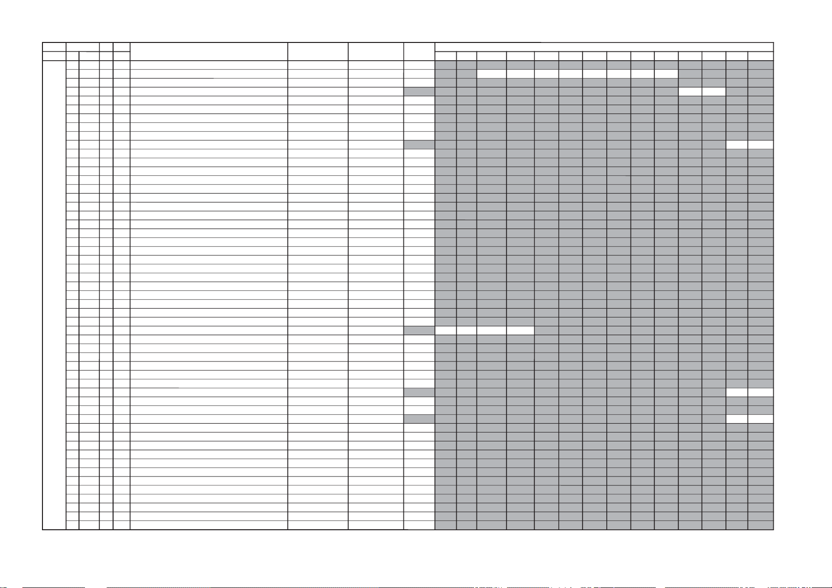
ceDceD 05)3.4(06)3:4(ZW05)9:61(ZW06)9:61(N05)9:61(N06)9:61(F05)9:61(F06)9:61(Z05)9:61(Z06)9:61(zH05buSzH06buSVToediV
PIP
000SPH
150552noitisoPerutciPlatnoziroH X8829ADS
100SPV
720552noitisoPerutciPlacitreV
200PFV
800510noitisoPeniFlacitreV
300PFH
510510noitisoPeniFlatnoziroH
)ciPbuS(zH06/05
400PSV
000100noitcudeResioNesluPcnySlacitreV
500LDV
000130yaleDesluPcnySlacitreV
600YLD
100510yaleDyaleS
700VGA
110510eulaVlortnoCniaGcitamotuA
800DPC
000300noitaruDgnipmalC
900LLP
000300tnatsnoCemitLLPtresnI
oediV/VT
010DCY
210510yaleDC/Y
110LIK
000300dlohserhTrellikroloC
210PGB
000100noitisoPetaGtsruB
310MED
100300noitcleSesahpmeeD
410AMC100300hctiwdnaBamorhC
510CFI
200300retliFnoitasnepmoCFI
610EUH
230360lortnoCEUH
710ACS
600130tnemtsujdAreirracbuSroloC
810NOC
000510tnemtsujdAtsartnoC
910TRB
000510tnemtsujdAssenthgirb
020RKP
331552deRleveLkaeP
120GKP
331552neerGleveLkaeP
220BKP
331552eulBleveLkaeP
320YRF
510510YroloCemarF
420TAS
700510tnemtsujdAnoitarutaSroloC
520KPY
300700tnemtsujdAgnikaePY
620OCY
100100elbanEgniroCY
72012P
0007001LDILAPdna2LDILAP
820LAP
000100leveLDILAP
920VOP
000700lacitreVtesffOnoitisoP
030HOP
610130latnoziroHtesffOnoitisoP
130LPC
100300htgneLesluPgnipmalC
230LRS
000300leveLnoitcejeRmaceS
330LIS
700700leveLnoitakifitnedImaceS
430DES
100100redividmaceS
530AFB
100100tnemtsujdAretliflleB
63021P
0003002dna1tnemercnILAP
730SOL
100300deepSgnikcoL
oediV/VT
830LAS
000700leveLecnatpeccAmaceS
930AES
000100ecnatpeccAmaceS
040RSN
000700LLPlatnoziroHroFnoitcudeResioN
oediV/VT
140HLS
000300HdlohserhTleveLgnicilS
240JAI
000300LLPlatnoziroHroFtnemtsujda-I
34005V
000721zH05gninepOnoisserppuSesioNwodniWlacitreV
44006V
230721zH06gninepOnoisserppuSesioNwodniWlacitreV
540SNV
000510zH06gnisolCnoisserppuSesioNwodniWlacitreV
640CSV
000510zH05gnisolCnoisserppuSesioNwodniWlacitreV
740TVS
510510VTLS&ytiraloPVdlohserhTleveLgnicilS
840MFV
000300edoMleehwylFlacitreV
940WFV
000100leehwylFlacitreV
050SVL
000300noitarapes-cnySlacitreVrofssapwoL
150ALC
300300ycnetalgnipmalC
250PCS
400130esluPgnipmalCfotratS
– 28 –
(Not used for this model)
RM-GA002
JVTytilanoitcnuF.tinIegnaRnoitcnuFetoN&elbaTemaNeciveDnommoC
yrogetaC.oNemaNceDceD
VTH000XAMV000360)XAMV+53=XAM(leveLemuloVmumixaM leveLemuloV00
100INIV520130norewoPtaleveLemuloVlaitinI leveLemuloV00
200YBTS000100 )YBTSsyawla=1,sutatsrewoptsalehtwollof=0(sutatSrewoPtsaL rewoPtsaL00
300GRPI100721)sledoMitluMrofylno(norewoPtarebmuNmargorPlaitinI rebmuNmargorP00
JVTytilanoitcnuF.tinIegnaRnoitcnuFetoN&elbaTemaNeciveDnommoC)deliateD(eulaVlaitinI
yrogetaC.oNemaNceDceD 05)3:4(06)3:4(srehtOVUY
MTPO000THSA600700)nim5*atad(remitffotuhsotuA 70/00
100BDSO510130ssenthgirbDSO h06orciM/RMM61
200HDSO800510noitisoPlatnoziroHDSO h06orciM/ATADX80
300VDSO730360noitisoPlacitreVDSO
)06/05(9:61<>06/053:4<
>)lluFlamroN()mooZediW()ediW(
h06orciM/RMM
1623
400ETUM000100)delbane=1(hctiwSetuMlangiSoN 10/00
500LUFR510510)hf0nehwelbasiD(dekcolnUretfaretnuoCegnahClangiSFR 10/40
600KLFR510510)hf0nehwelbasiD(dekcoLretfaretnuoCegnahClangiSFR 40/00
700GNAL000300noitidnocgnippihsegaugnalDSO 00
800TXTH000100wsrotarepescnyS srehto/VUYrossecorP-VT
0000
900SSMC000100wscnyS rossecorP-VT10
010OXCD060721eulaVOXCD PSD/h06orciM/RFS35/*
110CSID821552cedrolocybtsujdaOXCDrofatadOCSIDtegrat 821
210LBXE000510esioNetihWetanimilEotremiTgniknalBdednetxE 40/80
310SYST000300 )ledoMAG(]M:3,K/D:2,I:1,G/B:0[teseRtseTtaMVNnisySVTeziromeM 00
410WSNL100100)ffO:0,otuA:1(noitidnocteseRtseT/gnippihSretsooBlangiS 10
510LBL100100noitidnoclangiSoNtAnoitcudeRssenthgirB 10
610ORPH100100noitatoRerutciProftesffOarapH 50
710LUVA510510)hF0nehwelbasiD(dekcolnUretfaretnuocegnahclangisvA 40
810KLVA510510)hF0nehwelbasiD()dekcolretfaretnuocegnahclangisvA -/00
910MPSC000100 )edompotselbasid:1,edompots:0(ybdnatsniedompotselbasiD 10
020HNES000100)nO:1,ffO:0(m/cdnuosgnilkcarCrecnahnEdnuoS 10
120CSPS100300)semit8:3,semit6:2,semit4:1,elbasid:0(hcraeSDEEPS 10
220OLUM100100)woLevitcA:1,hgiHevitcA:0(noitceleScigoLtroPetuMoiduA 10
– 29 –
(For '*' refer to page 32)
KV-SZ252M50/M61/M81/N50/N60
RM-GA002
 Loading...