

Page 1
REVISION HISTORY
BX1L
CHASSIS
MODEL
KV-SZ252M50
KV-SZ252M61
KV-SZ252M81
KV-SZ252N50
KV-SZ252N60
NO. SUFFIX DATE SUPP / CORR DESCRIPTION
1 -01 2007/04 _ _ 1st Issue
PART NO.: 9-872-963-01
Page 2
SERVICE MANUAL
BX1L
CHASSIS
MODEL COMMANDER DEST. CHASSIS NO.
KV-SZ252M50 RM-GA002 E SCC-V66P-A
KV-SZ252M61 RM-GA002 GE SCC-V44U-A
KV-SZ252M81 RM-GA002 Middle East SCC-V83H-A
KV-SZ252N50 RM-GA002 Philipines SCC-V80K-A
KV-SZ252N60 RM-GA002 Philipines SCC-V80J-A
MODEL COMMANDER DEST. CHASSIS NO.
RM-GA002
TRINITRON
®
COLOR TV
Page 3

KV-SZ252M50/M61/M81/N50/N60
RM-GA002
TABLE OF CONTENTS
Section Title Page
SELF DIAGNOSTIC FUNCTION ........................................... 3
1. DISASSEMBLY
1-1. Rear Cover Removal..................................................5
1-2. Speaker Removal ....................................................... 5
1-3. Chassis Assy Removal ............................................... 5
1-4. Service Position ......................................................... 5
1-5. A and H2 Board Removal ......................................... 5
1-6. Picture Tube Removal................................................ 6
2. WIRE DRESSING
2-1. Lead Assy, Jumper Wire Dressing at A board...........7
2-2. Lead Assy, Jumper Wire Dressing at A board
(only for Audio 6+6 Non DSP models) .................... 7
2-3. Wire Dressing at A and H2 board ............................. 7
2-4. Dressing of Conn Assy, 4P VH ................................. 8
2-5. Dressing of Conn Assy, 5P YUV ............................... 8
2-6. Dressing of Conn Assy, 4P VM and
Connector Assy, 5P Front In...................................... 8
2-7. Installation and Dressing of Earth Assy Coating ...... 8
2-8. Installation and Dressing of Earth Assy Coating ...... 9
2-9. Insertion of Lead Assy, H Static................................ 9
2-10. Dressing of Conn Assy, 5P Front In .......................... 9
2-11. Dress Lead Assy, Earth and Conn Assy,
5P In with Purse Lock Ø 5 ...................................... 10
2-12. CV Board Connector Assy Wire Dressing.............. 10
2-13. Connector Assy Wire Dressing................................10
2-14. Connector Assy Wire Dressing................................11
2-15. Overall V iew of Rotation Coil Conn Dressing ....... 11
2-16. Overall View of Lead Assy, G2; Lead Assy, Focus
and Rotation Coil Conn Dressing ........................... 11
2-17. Dress Lead Assy, Speaker to Rotation Coil using
Purse Lock Ø 9 ........................................................ 12
2-18. Dressing of PF Board Conn Assy (for models
with PF board only) ................................................. 12
2-19. Cap Assy, High Voltage Installation ........................12
2-20. HV Cap Assy Wire Dressing ................................... 13
2-21. AC Power Cord Wire Dressing ............................... 13
Section Title Page
4. CIRCUIT ADJUSTMENTS
4-1. Adjustment With Commander ................................18
4-2. Adjustment Method ................................................19
4-3. Picture Quality Adjustment .................................... 36
4-3-1. P Max/Contrast Adjustment .........................36
4-3-2. Sub Color Adjustment ..................................36
4-3-3. Sub Hue Adjustment ....................................36
4-4. Geometry Adjustment .............................................37
4-4-1. H-Trapezoid Adjustment ..............................37
4-4-2. Normal Mode 50Hz/60Hz ............................ 37
4-4-3. Wide Mode 50Hz/60Hz
(V Compression Adjustment)................................ 37
5. DIAGRAMS
5-1. Block Diagram ......................................................... 38
5-2. Circuit Boards Location .......................................... 39
5-3. Schematic Diagram Information ............................. 39
5-3-1. A Board — (Block 001)............................... 40
5-3-2. A Board — (Block 002)............................... 42
5-3-3. A Board — (Block 003).............................. 44
5-3-4. A Board — (Block 004)............................... 46
5-3-5. A Board — (Block 005)............................... 48
5-3-6. A Board — (Block 006)............................... 50
5-3-7. A Board — (Block 007)............................... 52
5-3-8 CV Board Schematic Diagram ..................... 53
5-3-9. H2 Board Schematic Diagram...................... 55
5-4. Voltage Measurement and Waveform...................... 57
5-5. Printed Wiring Boards ............................................. 61
5-6. Semiconductors........................................................ 67
6. EXPLODED VIEWS
6-1. Chassis ..................................................................... 69
7. ELECTRICAL PARTS LIST .......................................... 71
OPERATING INSTRUCTIONS
3. SET-UP ADJUSTMENTS
3-1. Beam Landing Adjustment...................................... 14
3-2. Convergence Adjustment.........................................15
3-3. Focus Adjustment .................................................... 17
3-4. G2 (SCREEN) Adjustments ....................................17
3-5. Sub Bright Adjustment ............................................ 17
3-6. White Balance Adjustment...................................... 17
CAUTION
SHORT CIRCUIT THE ANODE OF THE PICTURE TUBE AND THE
ANODE CAP TO THE METAL CHASSIS, CRT SHIELD, OR
CARBON PAINTED ON THE CRT, AFTER REMOVING THE
ANODE.
SAFETY-RELATED COMPONENT WARNING!!
COMPONENTS IDENTIFIED BY SHADING AND MARK ! ON THE
SCHEMATIC DIAGRAMS, EXPLODED VIEWS AND IN THE
PARTS LIST ARE CRITICAL TO SAFE OPERATION. REPLACE
THESE COMPONENTS WITH SONY PARTS WHOSE PART
NUMBERS APPEAR AS SHOWN IN THIS MANUAL OR IN
SUPPLEMENTS PUBLISHED BY SONY.
– 2 –
Page 4
KV-SZ252M50/M61/M81/N50/N60
SELF DIAGNOSTIC FUNCTION
The units in this manual contain a self-diagnostic function. If an error occurs, the STANDBY Indicator will automatically
begin to flash.
The number of times the STANDBY Indicator flashes translates to a probable source of the problem.If an error symptom
cannot be reproduced, the remote commander can be used to review the failure occurrence data stored in memory to
reveal past problems and how often these problems occur.
1. DIAGNOSTIC TEST INDICATORS
When an error occurs, the STANDBY Indicator will flash a number of times to indicate the possible cause of the
problem. If there is more than one error, the Indicator will identify the first of the problem areas.
Result for all of the following diagnostic items are displayed on screen. No error has occured if the screen displays a “0”.
RM-GA002
Diagnosis
Item
Description
• No Power
• +B overcurrent
(OCP)
•Vertical NG.
• IK (AKB)
No. of times
STANDBY
Indicator flashes
Does not light
2 times
4 times
5 times
Diagnostic Result
on screen display
—
2 OCP:0
2 OCP:1 ~ 255
4 VSTOP:0
4 VSTOP:1 ~ 255
5 AKB:0
5 AKB:1 ~ 255
Probable
Cause
Location
•Power cord is not plugged
in.
• Fuse is burned out (F4101)
(H2 Board)
• H.OUT (Q511) is shorted.
(A board)
• IC751 is shorted.
(C/CV Board)
• +13V is not supplied.
(A Board)
• IC503 voltage list is faulty.
(A Board)
• Video OUT (IC751) is faulty.
(CV Board)
• IC001 is faulty. (A Board)
• Screen (G2) is improperly
adjusted.
Detected
Symptoms
•Power does not turn on.
•No power is supplied to the
TV.
•AC power supply is faulty.
•Power does not turn on.
•Load on power line is
shorted.
•Has entered standby state
after horizontal raster.
•Vertical deflection pulse is
stopped.
•Power line is shor ted or
power supply is stopped.
•No raster is generated.
•CRT cathode current
detection reference pulse
output is small.
• Supply Voltage
Protection
8 times
8 SUP:0
8 SUP:1 ~ 255
2. STANDBY INDICATOR BLINKING PROCESS
Lamp ON 300ms
Lamp OFF 300ms
The example above represents for 4 times blink
Lamp OFF 3 seconds
• IC604 faulty.
• IC607 faulty.
•No power supply to CRT
ANODE.
•No RASTER is generated.
3. STANDBY INDICATOR ON TV FRONT PANEL
Standby indicator
– 3 –
Page 5
KV-SZ252M50/M61/M81/N50/N60
RM-GA002
4. SELF DIAGNOSTIC SCREEN DISPLAY
SELF DIAGNOSTIC
2 : 000
3 : N/A
4 : 000
5 : 001
8 : 002
101 : N/A
5. HANDLING SELF DIAGNOSTIC SCREEN DISPLAY
No. Description Method
1. Display self diagnostic screen [Display] t [Channel ] t [Volume ] t [Power / TV]
2. Stop standby flash i) Turn off power switch on main.
3. Clear fault result In self diagnostic screen, press [Channel ] t -
4. Quit self diagnostic screen Turn off power switch of remote commander or main unit.
"0" means no fault has been detected.
"1" means a fault has been detected.
"2" means two faults has been detected.
"N/A" means not available for this models.
5
Note: The above must be performed while TV is on standby mode.
ii) Unplug power cord from the outlet.
8
Note: Diagnostic results display on screen is not automatically cleared. Therefore,
clear result after completion of repair.
6. SELF-DIAGNOSTIC CIRCUIT
A BOARD
IC003
MEMORY
5
SDA
FROM
CV BOARD
IC751 PIN 5
A BOARD
FROM
Q816
COLLECTOR
A BOARD
IC001
Y/CHROMA JUNGLE
IK
32
EHT0
A BOARD
IC503
V.OUT
F.B-PLS
A BOARD
IC001
SYSTEM
SDA1
3 1384
V.GUARD
RED LED
99
122
DISPLAY
[+B overcurrent $OCP%] Occurs when an overcurrent on the +B(135V) line is detected by pin 32 of IC001 (A board).
If the voltage of pin 32 of IC001 (A board) is more than 4V, the unit will automatically go to
standby.
[V-PROTECT] Occurs when an absence of the vertical deflection pulse is detected by pin 13 of IC001
(A board).
[IK $AKB%] If the RGB levels* do not balance within 15 sec after the power is turned on, this error will be
detected by IC001 (A board). TV will stay on, but there will be 5 times LED blinking.
POWER SUPPLY NG (+5V)
for VIDEO PROCESSOR
Occurs when IC001 internal HV protect detects an abnormal H-Pulse (frequency) due to
improper power supply to IC001. TV cuts off high voltage power of anode CRT. No picture will be
detected. eg: IC602, IC604 go faulty.
* (Refers to the RGB levels of the AKB detection Ref pulse that detects IK.)
– 4 –
Page 6
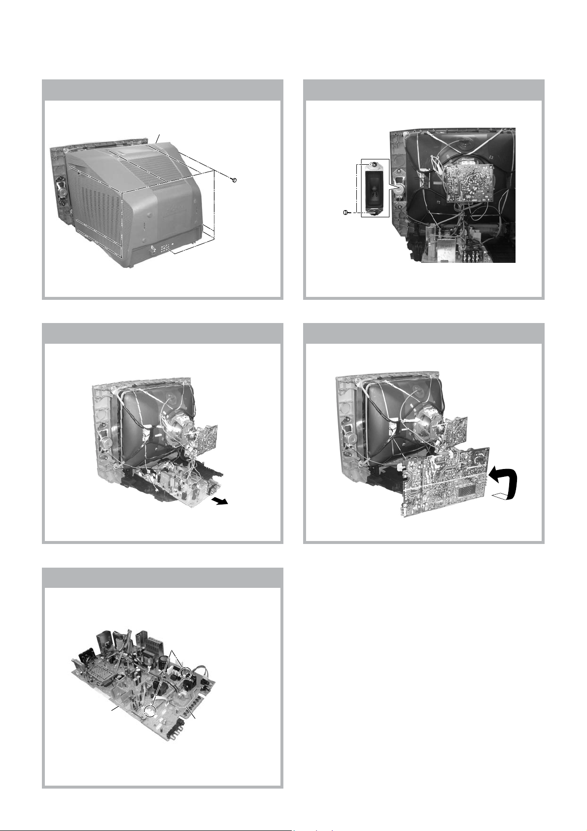
SECTION 1
DISASSEMBLY
KV-SZ252M50/M61/M81/N50/N60
RM-GA002
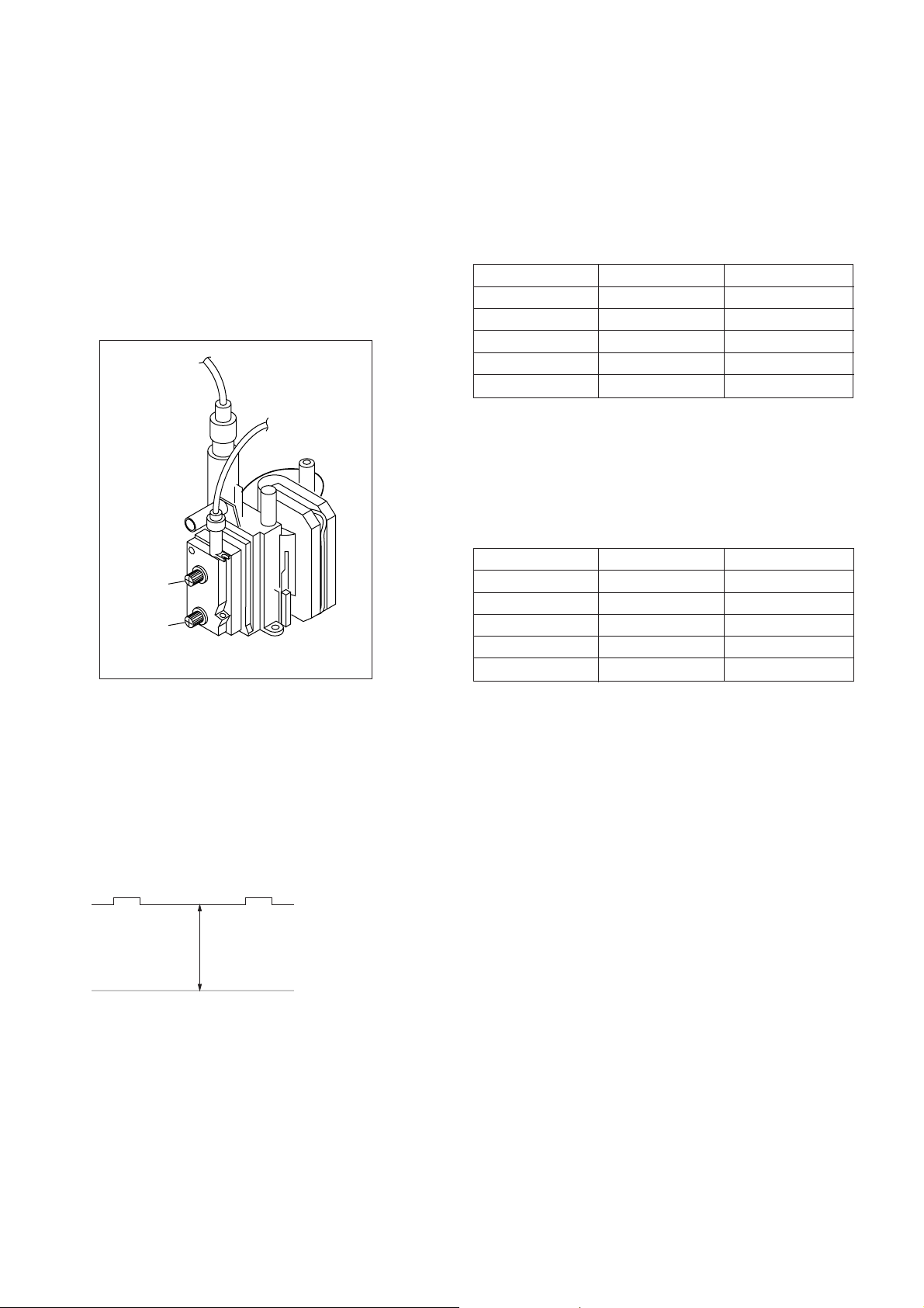
1-1. REAR COVER REMOVAL
2 Rear cover
1 Nine screws
(+BVTP 4 × 16)
1-2. SPEAKER REMOVAL
1 Two screws
(Tapping screw)
(+PWH 4x16)
1-3. CHASSIS ASSY REMOVAL 1-4. SERVICE POSITION
1-5. A AND H2 BOARD REMOVAL
1 Two hooks
3 A Board
2 H2 Board
– 5 –
Page 7
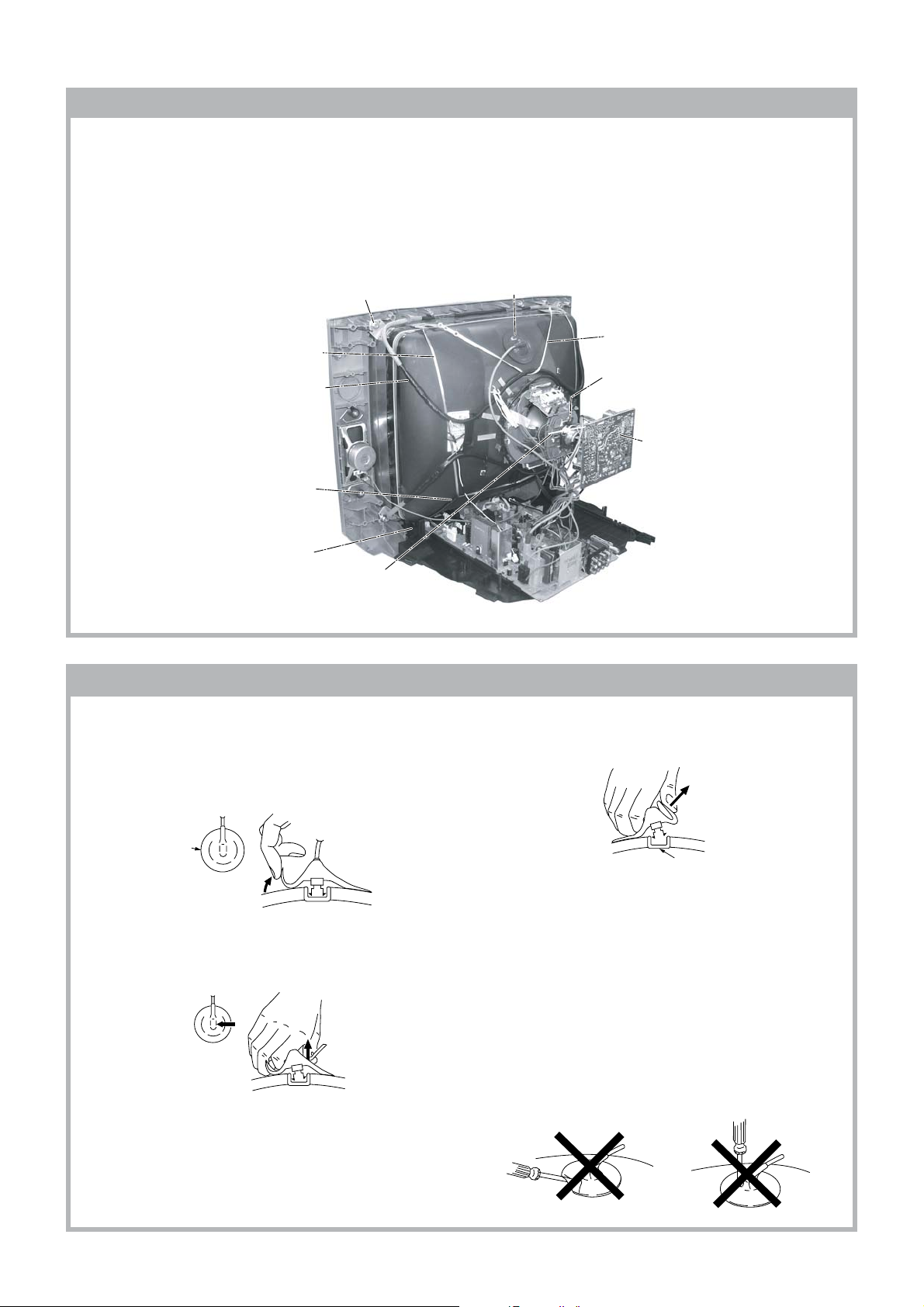
KV-SZ252M50/M61/M81/N50/N60
RM-GA002
1-6. PICTURE TUBE REMO VAL
Note:
• Please make sure the TV set is not in standing position bef ore removing necessary CRT support located on bottom
right and left.
1) Remove the rear cover.
2) Unplug all interconnecting leads from the Deflection yoke, Neck assy, Degaussing Coil and CRT grounding strap.
Remove Chassis Assy.
3) Place the TV set with the CRT face down on a cushion jig.
qd Screw Tapping
7+ Crown Washer (x4)
0 Earth Coating Assy
9 Degaussing Coil
8 Spring Tension(x2)
Removal
qs Supports CRT (x2)
Removal
qa Loosen the Deflection Yoke
fixing screw and remove
4 Anode Cap Removal
7 Band, DGC Removal
6 Loosen the Neck Assembly
fixing screw and remove
Neck Assy
5 CV Board Removal
• REMOVAL OF ANODE-CAP
Note:
• After removing the anode, short circuit the anode of the picture tube and the anode cap to the metal chassis, CRT
shield or carbon paint on the CRT.
• REMOVING PROCEDURES
a
a
1 Turn up one side of the rubber cap in the direction
indicated by the arrow a.
b
b
2 Using a thumb pull up the rubber cap firmly in the direc-
tion indicated by the arrow b.
c
Anode Button
3 When one side of the rubber cap is separated from the
anode button, the anode-cap can be remo ved by
turning up the rubber cap and pulling it up in the
direction of the arrow c.
• HOW TO HANDLE AN ANODE-CAP
1 Do not damage the surface of anode-caps with
sharp shaped objects.
2 Do not press the rubber too hard so as not to
damage the inside of anode-cap.
A metal fitting called the shatter-hook terminal is
built into the rubber.
3 Do not turn the foot of rubber over too hard.
The shatter-hook terminal will stick out or damage
the rubber.
– 6 –
Page 8
KV-SZ252M50/M61/M81/N50/N60
RM-GA002
SECTION 2
WIRE DRESSING
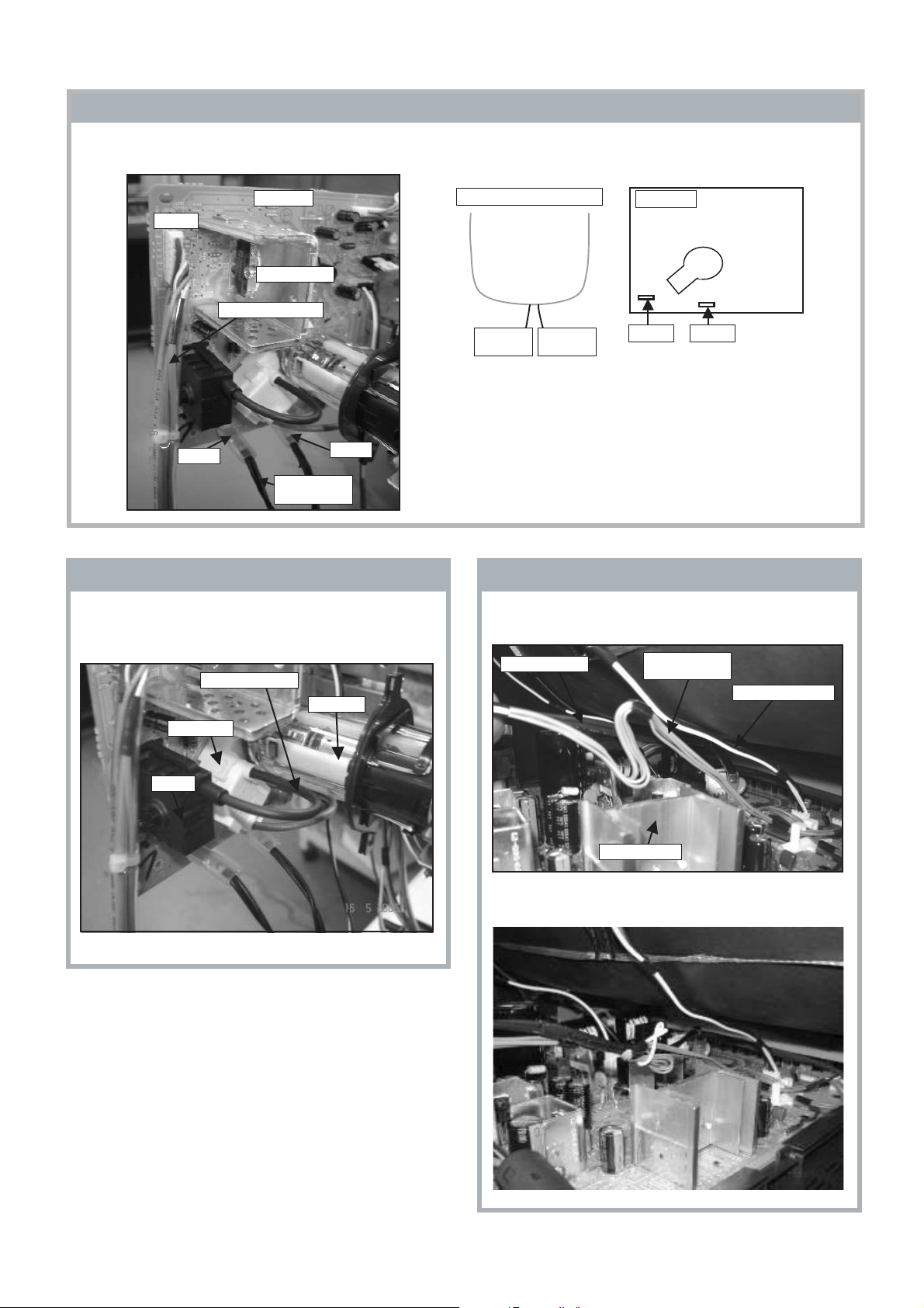
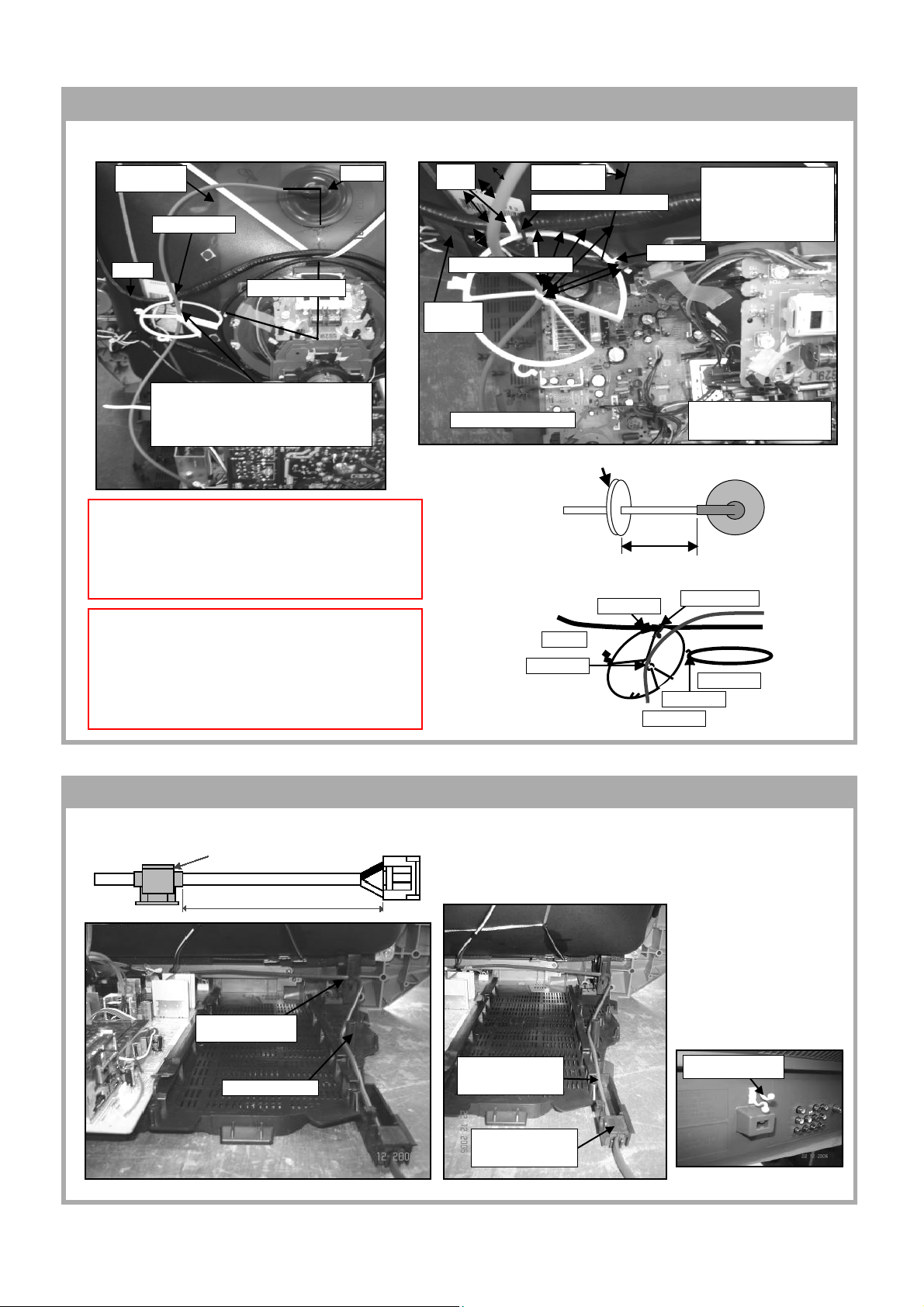
2-1. Lead Assy, Jumper Wire Dressing at A board
W082
P/N 1-923-512-11
W016
Keep Lead Assy, Jumpers
away from R121
W077
Dress both Lead Assy, Jumpers
along edge of shield case
P/N 1-910-026-28
Conn Assy,
5P YUV
CAUTION :
1. Do not ov erpull the wires during dressing
--> avoid disconnection of wires.
2. Make sure wires are kept away from
sharp edges, heatsinks & other
high-temperature parts.
2-2. Lead Assy, Jumper Wire Dressing at A board
(only for Audio 6+6 Non DSP models)
L2601
A002
W075
C211
Dress Lead Assy,
Jumper around C249
P/N 1-910-036-25
Dress Lead Assy, Jumper in
between C211 and L2601
UL Tube
A003
Dress between
T501
C514
W084
W065
No. Part No. Description Block Remark
1 1-910-026-28 Lead Assy, Jumper A(Var)
W077-W065(0)
2 1-923-512-11 WIRE UL1007 AWG24 150MM ORG A(Com) W082-W010(1)
CN905
W010
C903
Dress Lead Assy, Jumper far
away from C514 and T501
Dress both Lead
Assy, Jumpers
around CN905, C903
and below Conn
Assy, 5P YUV
W016-W084(1)
No. Part No. Description Block Remark
2 1-910-036-25 Lead Assy, Jumper A(Var) W075-W085(1)
A003 and A002
W085
2-3. Wire Dressing at A and H2 board
i) Insert and dress Conn Assy, 4P into hook. ii) Insert Conn Assy, 5P into CN4105.
Make sure AC Power Cord is behind Lead Assy,
Speaker at CN4106.
AC Power Cord is behind
Lear Assy, Speaker
Conn Assy, 4P
CN4110
1
CN2105
Conn Assy, 7P
Insert Conn Assy,
4P into hook
CN4113
CN3102
Lead Assy, Speaker
CN4105
2
CN4106
Conn Assy, 5P
– 7 –
TVSR:
Connector assy must be kept away
from primary area(10mm minimum).
Page 9
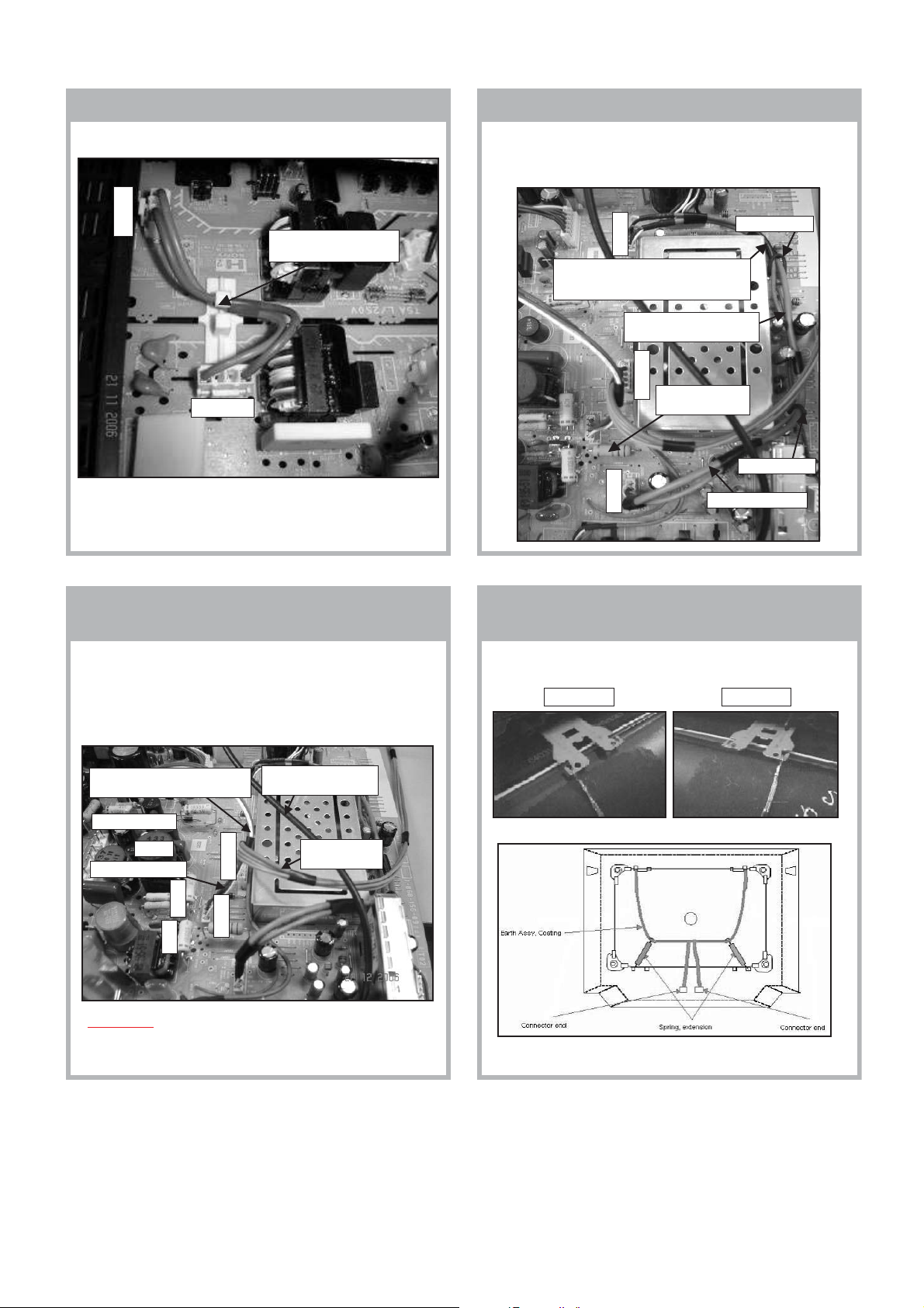
KV-SZ252M50/M61/M81/N50/N60
RM-GA002
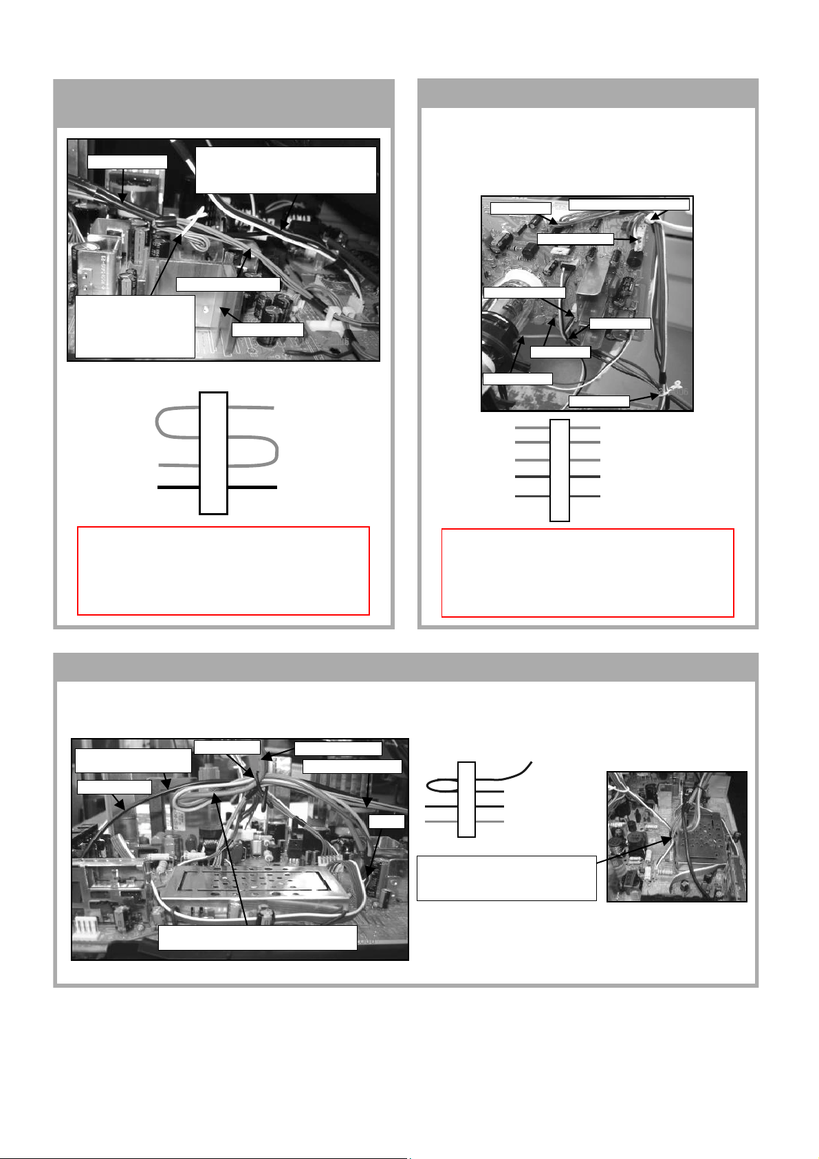
2-4. Dressing of Conn Assy, 4P VH
Dress Conn Assy, 4P VH into hook as shown.
CN4102
Insert Connector Assy,
4P VH into holder
CN6101
2-5. Dressing of Conn Assy, 5P YUV
Dress Conn Assy, 5P YUV around shield case.
Use pin, wires A019 and A017 to dress Conn Assy,
5P YUV as shown.
Pin, wire A019
CN007
Make sure the UL tape is positioned at
the sharp edge of shield case to prevent
wire from being scratched
Dress Conn Assy, 5P YUV
around shield case
CN9201
Keep wires away
from R121
CN905
Pin, wire A017
Conn Assy, 5P YUV
2-6. Dressing of Conn Assy, 4P VM and
Connector Assy, 5P Front In
Dress Conn Assy, 4P VM behind Conn Assy, 5P Front In
as shown.
Conn Assy, 5P Front In is used to prevent Conn Assy,
4P VM from bending towards T504, R579 and R5032
(high temperature parts).
Dress Conn Assy, 4P VM behind
Conn Assy, 5P Front In
Deflection area
T504
Conn Assy, 4P VM
R5032
CN003
R579
CAUTION:
Keep Conn Assy, 5P Front In away from deflection area
(T504, R5032, etc.) when dressing.
Lead Assy, Earth is
above Conn Assy, 5P
CN9201
Conn Assy, 5P
Front In
2-7. Installation and Dressing of Earth Assy
Coating
i) Earth Assy, Coating is installed as shown.
Right side Left side
– 8 –
Page 10
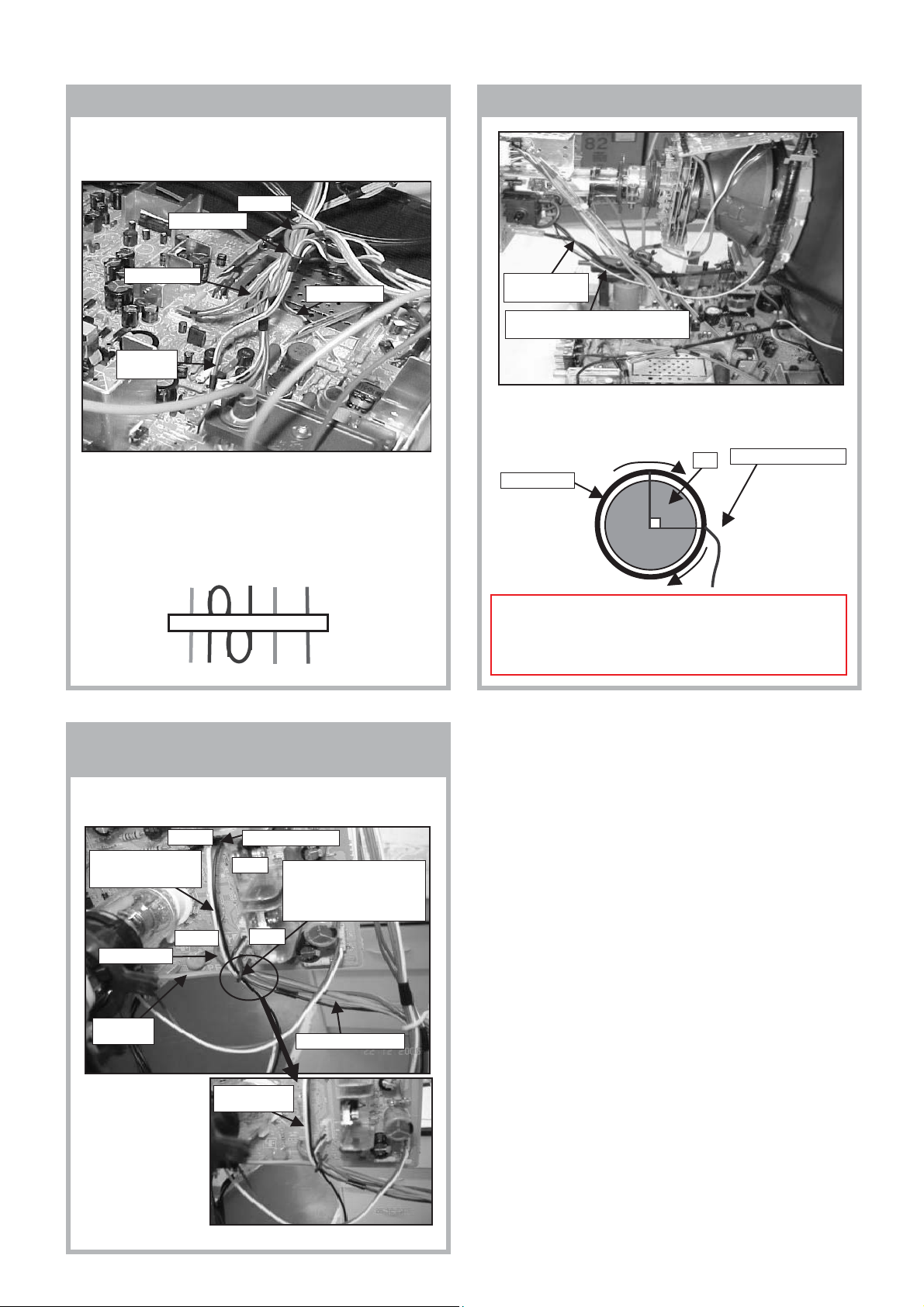
2-8. Installation and Dressing of Earth Assy Coating
ii) Insert the 2 Earth Assy, Coating wires to CN705 &
CN707 as shown. Insert Conn Assy, 7P RGB into CN701.
KV-SZ252M50/M61/M81/N50/N60
RM-GA002
CV board
CN701
Heatsink A751
Conn Assy, 7P RGB
CN707
Coating wires
CN705
Earth Assy,
2-9. Insertion of Lead Assy, H Static
Insert Lead Assy, H Static into CRT socket and RV750 as
shown. Make sure the wire is naturally curved, to avoid
touching CRT neck.
Lead Assy, H static
CRT neck
CRT socket
Earth Assy, Coating dressing
BLK+BLK
to CN705
BLK+BLK
to CN707
CV board
CN707 CN705
2-10. Dressing of Conn Assy, 5P Front In
Make a 'S' shaped loop on Conn Assy, 5P Front In
as shown. Keep wires away from heatsink A010.
Lead Assy, Earth
Conn Assy, 5P
Front In
Lead Assy, Speaker
RV750
Heatsink A010
Next, Conn Assy, 5P Front In is dressed together with
Lead Assy,Earth using purse lock Ø 5. Refer to next page.
– 9 –
Page 11
KV-SZ252M50/M61/M81/N50/N60
RM-GA002
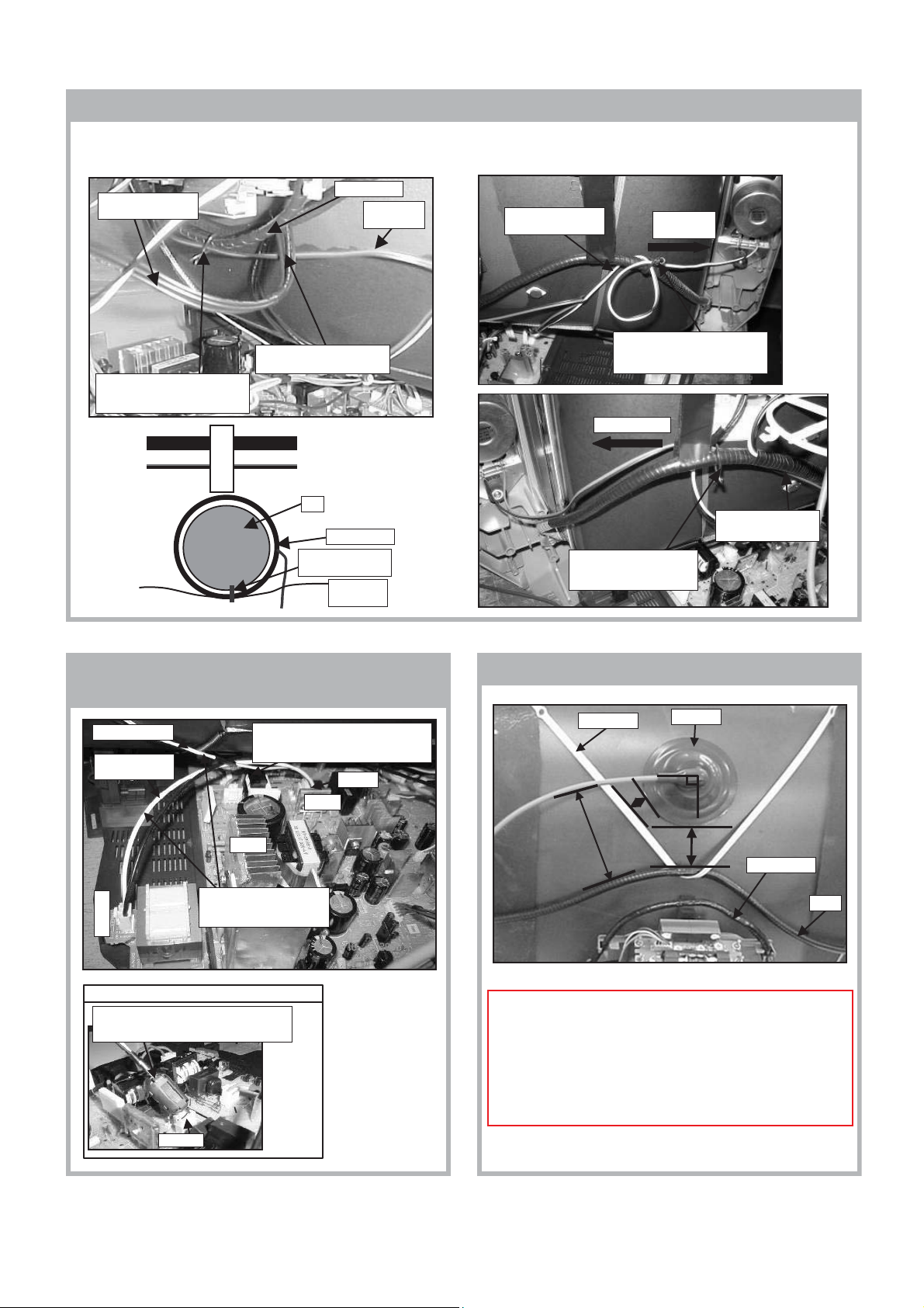
2-11. Dress Lead Assy, Earth and Conn Assy,
5P In with purse lock
Lead Assy, Earth
Make a 'S' shaped loop on
Conn Assy, 5P Front In
and dress together with
Lead Assy, Earth using
purse lock Ø 5
Note: Dress while chassis is halfway docked into beznet.
together with purse lock. Keep Lead Assy,
Conn Assy, 5P Front In
Ø
5
Lead Assy, Speaker is not dressed
Speaker away from heatsink A010 by
dressing it close to the CRT
Heatsink A010
Conn Assy,
Purse lock Ø 5
5P Front In
Lead Assy, Earth
2-12. CV Board Connector Assy Wire Dressing
i) Dress Conn Assy, 6P and Conn Assy, 4P VM using tie,
cable at alignment hole 'B' on CV board as shown.
ii) Dress Conn Assy, 4P 200V; Conn Assy, 6P; Conn Assy,
4P VM; Lead Assy, G2 and Lead Assy, Focus with purse
lock Ø 5.
Conn Assy, 6P
Conn Assy, 4P 200V
Lead Assy, Focus
Tie, cable at alignment hole 'B'
Conn Assy, 4P VM
Pin, wire A707
Lead Assy, G2
Purse lock Ø 5
Purse lock Ø 5
Conn Assy, 4P VM
Conn Assy, 4P 200V
Conn Assy, 6P
Lead Assy, Focus
Lead Assy, G2
CAUTION:
Prevent tie, cable from touching rear cover or any
enclosures by turning them away from it --> avoid
rattle sound. Also prevent tie, cable's end from
touching solder side of board.
2-13. Connector Assy Wire Dressing
i) Dress Conn Assy, 7P RGB; Conn Assy, 5P Front In and
Lead Assy, Earth using purse lock Ø 9. Keep wires away from
heatsinks and high-temperature parts.
Lead Assy, Earth is behind
Conn Assy, 7P RGB
Lead Assy, Earth
Make loop of Conn Assy, 7P RGB as large as
possible when dressing with purse lock
Purse lock Ø 9
Conn Assy, 7P RGB
Conn Assy, 5P Front In
CN004
CAUTION:
Prevent tie, cable from touching rear cover or any
enclosures by turning them away from it --> avoid
rattle sound. Also prevent tie, cable's end from
touching solder side of board.
Conn Assy, 7P RGB
Lead Assy, Earth
Conn Assy, 5P Front In
Purse lock Ø 9
Keep Conn Assy, 5P Front In wire in an upward
path from CN9201 to where it is dressed with
purse lock Ø 9. This is to keep it away from
deflection area.
– 10 –
Page 12
KV-SZ252M50/M61/M81/N50/N60
RM-GA002
2-14. Connector Assy Wire Dressing
Dress DY Connector; Conn Assy, 4P 200V;
Conn Assy 4P VM and Conn Assy, 6P using purse lock
Ø 9 as shown.
DY Conn
Purse lock Ø 9
Conn Assy, 6P
Conn Assy, 4P
Conn Assy,
4P 200V
Note: Make sure DY connector is inserted securely.
--> prevent it from coming out.
2-15. Overall View of Rotation Coil Conn Dressing
Earth Assy,
Coating wires
Rotation coil conn is dressed outside
and below Earth Assy, Coating wires.
Install Rotation Coil as shown.
1) Coil positioned in clockwise direction.
2) Wire is at 3 o'clock position.
Wire from Roation Coil
DY
Rotation Coil
DY Connector
Conn Assy,
4P VM
Purse lock Ø 9
Conn Assy,
4P 200V
Conn Assy, 6P
2-16. Overall View of Lead Assy, G2; Lead Assy,
Focus and Rotation Coil Conn Dressing
Avoid any stress on Lead Assy, G2; Lead Assy, Focus and
terminal at W7001.
CN1802
Keep wire away
from R781 and
heatsinks A713, A715.
W7001
Lead Assy, G2
Lead Assy,
Focus
Rotation Coil Conn
A715
connector together with Lead
Assy, G2; Lead Assy Focus
and Conn Assy, 4P 200V
A713
Conn Assy, 4P 200V
Dress Rotation Coil
using pin, wire A707
CAUTION:
Prevent wires from touching rear cover or any
enclosures by turning them away from it--> avoid rattle
sound.
Keep wire away
from R781
– 11 –
Page 13
KV-SZ252M50/M61/M81/N50/N60
RM-GA002
2-17. Dress Lead Assy, Speaker to Rotation Coil using Purse Lock Ø 9
Dress Lead Assy, Speaker to center position of Rotation Coil using purse lock Ø 9 as shown. Make sure Earth
Assy, Coating wire is above Lead Assy, Speaker. This is to keep Lead Assy, Speaker away from Deflection Yoke.
Earth Assy, Coating
wire
Dress Lead Assy, Speaker to
center position of Rotation Coil
using purse lock Ø 9
Purse lock Ø 9
Rotation coil
Lead Assy,
Earth Assy, Coating wire is
above Lead Assy, Speaker
Rotation Coil
Lead Assy, Speaker
(RED+BLK)
DY
Rotation Coil
Attach purse lock Ø 9
here
Lead Assy,
Speaker
Speaker
Lead Assy, Speaker
goes behind DGC
Dress Lead Assy, Speaker
directly on to DGC using
Pull wire to
the right
Loop Lead Assy, Speaker and
dress directly on to DGC using
purse lock
Pull wire to left
purse lock Ø 9
Ø 9
Lead Assy, Speaker
goes behind DGC
2-18. Dressing of PF Board Conn Assy
(for models with PF board only)
DGC Connector
Connector Assy,
3P VH
heatsinks A007, D604 and
CN6620
Apply to all SZ252 Narrow 220V CISPR models ONLY
Clamp the ferrite core at the end of the DGC
wire as shown. Position it directly above DGC
Connector's housing
DGC Connector is below Conn Assy,
3P VH to keep Conn Assy, 3P VH
away from Heatsink A007 and D604
D604
A007
Keep wires away from
conductive parts
CN605
2-19. Cap Assy, High Voltage Installation
DGC Band
>5mm
Keep distance of
1mm/kV
TVSR Requirement:
1. Keep HV cable away from conductive parts
(distance of 1mm/kV).
2. Keep spacing between edge of anode cap
& conductive parts (distance of 0.5mm/kV).
3. Keep spacing between edge of anode cap &
non-conductive parts (distance of at least 5mm or more).
HV Cap
90º
Keep distance of
0.5mm/kV
Rotation coil
DGC
Housing
– 12 –
Page 14
2-20. HV Cap Assy Wire Dressing
Dress Cap Assy, High Voltage with Holder, HV Cable combi as shown.
KV-SZ252M50/M61/M81/N50/N60
RM-GA002
CRT's carbon
area
purse lock Ø 9.
DGC
10 o'clock position
Dress Holder, HV Cable Combi to Cap Assy,
High Voltage and attach side hook to rotation
coil at 10 o'clock position. Then, attach large
hook to DGC and dress with
purse lock
Ø
9.
HV cap
90º
CAUTION: 1) Make sure the specified position is
being followed.
2) Position the Cap Assy, High Voltage in
the inner ring of the Holder, HV cable
combi (see diagram).
TVSR requirement:
1. Spacing between HV cable and other conductive
part's surface is 1mm/kV or more.
2. Spacing between HV cable's and enclosure with
ventilation or the edge where terminal bracket and
rear cover meet: 10mm or more.
Large
hook
Min. distance = 1mm/kV
P-P taping
of DGC
Min. distance = 1mm/kV
CRT's carbon
area
Dress using Purse lock Ø 9
Holder, HV cable combi
250 ± 5 mm
Large hook
DGC
Inner Ring
Dress Holder, HV Cable
Combi to the right of P-P
taping of DGC. Dress
purse lock
of large hook on Holder,
HV Cable Combi.
Side hook
Keep distance of HV cable
from other wires, conductive
parts and CRT's carbon area
Purse lock Ø 9
Rotation coil
Side hook
Top view
Ø
9 to the right
2-21. AC Power Cord Wire Dressing
Install AC cord holder to AC power cord at specified position as shown.
AC Cord Holder
290 ± 5mm 630 ± 5mm
Hook AC cord into
CRT support's hook
Make sure AC cord is
straight between
Dress behind boss
boss and holder
Attach AC cord onto
holder and insert to
bottom cover
Attach Purse Lock (S)
Ø 8 in to rear cover
– 13 –
Page 15
KV-SZ252M50/M61/M81/N50/N60
RM-GA002
SECTION 3
SET-UP ADJUSTMENTS
The following adjustments should be made when a complete
realignment is required or a new picture tube is installed.
Perform the adjustments in order as follows :
1. Beam Landing
2. Convergence
3. Focus
The controls and switch should be set as follows unless
otherwise noted:
4. G2(SCREEN)
5. White Balance
Picture Control....................................."NORMAL"
Brightness Control..............................."NORMAL"
Note : Test Equipment Required.
1. Pattern Generator 5. Oscilloscope
2. Degausser 6. Landing Checker
3. DC Power Supply 7. XCV Adjuster
4. Digital Multimeter
......................................................................................................................................................................................................................
Preparation :
•Feed in the white pattern signal.
6. Then move the DY forward and adjust so that the entire
screen becomes green.
• Before starting, degauss the entire screen with the
degausser.
• In order to reduce the geomagnetism on the set's picture
tube, face it east or west.
3-1. BEAM LANDING ADJUSTMENT
1. Input a raster signal with the pattern generator.
2. Loose the deflection yoke(DY) mounting screw, and set
the purity control to the center as shown below:-
Purity control
3. Position Neck Assy as shown below:-
Neck assy
Align the edge of
the neck assy with
the edge of the G2 grid.
G2G1 G3
4. Set the raster signal of the pattern generator to green.
5. Move the DY backward and adjust the purity control so
that green is in the center and blue and red are at the
sides evenly.
7. Now switch over raster signal to red then blue and
confirm the condition.
8. When the position of the DY is determined, tighten it with
the DY mounting screw.
9. If the beam does not land correctly in all the corners of
the screen, use magnet disc to correct it.
Purity control
corrects this area.
b
c
Deflection yoke positioning
corrects these areas.
a
a
d
d
Disc magnets or rotatable
disc magnets correct these
areas (a-d).
b
c
Red
Blue
Green
– 14 –
Page 16
KV-SZ252M50/M61/M81/N50/N60
RM-GA002
3-2. CONVERGENCE ADJUSTMENT
Preparation:
• Before starting, perform FOCUS adjustment.
• Picture Mode "CUSTOM"
• Receive dot/cross hatch pattern.
a) Vertical Static Convergence
Center dot
R G B
R
G
B
4 pole magnet
RV750
H. STAT
b) Horizontal Static Convergence
If the blue dots does not converge with the red and
green dots, use the 6 pole magnet to adjust in
the manner described below:-
RG B R G B R GB
RB
G
RG
6 Pole
Magnet
GB
RB
RV1800
G2 (SCREEN)
1. (Moving vertically), adjust the 4 pole magnet to
converge red, green and blue dots in the center of
the screen.
2. Tilt the 4 pole magnet and adjust static convergence
to open or close the 4 pole magnet.
3. When the 4 pole magnet is moved in the direction of
arrow A and B, the red, green and blue dots moves
as shown below:-
A
B B
A
B
G
R
B
B
G
R
Moved RV750 (H.STAT)
6 Pole Magnet
Purity
DY pocket
4 pole Magnet
4 Pole
Magnet
c) Y Separation axis correction magnet adjustment.
1. Receive cross hatch signal.
2. Set Picture to "MINIMUM", Brightness to "STANDARD".
3. Adjust the Y separation axis correction magnet on
the Neck Assembly so that the horizontal lines at
the top and bottom of the screen are straight.
Neck assy Neck assy
RedBlue
RedBlue
RGGRB
B
VM board VM board
– 15 –
Page 17
KV-SZ252M50/M61/M81/N50/N60
RM-GA002
d) Convergence Rough Adjustment
Preparation:
• Before starting this adjustment, adjust the
horizontal and vertical static convergence.
Input cross hatch pattern.
i) TLH
Adjust the horizontal convergence of red and blue
dots by inserting TLH Correction Plate to the DY
pocket(left or right).
ii) YCH
Adjust YCH to balance Y axis.
iii) TLV
Adjust the vertical convergence of red and blue dots.
iv) XCV
Adjust XCV to balance X-axis
B
R
TLH
(VR2)
YCH
RB
YCH
B
R
ON DY :
(VR1)
TLV1 (no need to adjust)
TLV
DY pocket
b1
a1
c1
d1
R
B
a1~d1: Piece A(90), Convergence Correct
or
Permaloy Assy Correction
XCV
(VR3)
TLV2
(XCV)
DY pocket
TLH Plate
e) Screen Corner Convergence
Affix a Piece A(90), Convergence Correct/Permaloy Assy
Correction to the misconverged areas.
ba
a-d : screen-corner
misconvergence
cd
– 16 –
Page 18
KV-SZ252M50/M61/M81/N50/N60
RM-GA002
3-3. FOCUS ADJUSTMENT
FOCUS adjustment should be completed before W/B
adjustment.
1. Receive digital monoscope pattern.
2. Set Picture Mode to "VIVID".
3. Adjust focus VR to obtain a just focus at the
center of the screen.
4. Change the receiving signal to white pattern
and blue back.
5. Confirm magenta ring is not noticeable. In case
magenta ring is obvious, then adjust FOCUS VR
to balance magenta ring and FOCUS.
3-5. SUB BRIGHT ADJUSTMENT
1. Set TV to RF mode.
2. Input PAL monoscope to RF mode (OTHER model) and
NTSC monoscope (NTSC model).
3. Set Brightness to 50% and Picture to "MINIMUM" in
"CUSTOM" mode.
4. Select WHBL 010 "SBRT" with 1 and 4 button and
adjust its data using 3 and 6 button so that the Cut Off
level and slightly glimmer is as the specification below:-
TV size Cut Off Slightly Glimmer
25" 10 IRE 20 IRE + 2 steps
29" 10 IRE 20 IRE + 2 steps
34" 10 IRE 20 IRE + 2 steps
28" 10 IRE 20 IRE
32" 10 IRE 20 IRE
5. Write into the memory by pressing [MUTING] t -.
6. Copy the adjusted data WHBL 010 “SBRT” to Video
mode.
7. Once adjustment is completed in RF and Video mode,
carry out adjustment in DVD mode. Repeat step 2 to 3.
Select WHBL 010 “SBRT” and adjust its data as the
specification below:-
Focus
Screen
FLYBA CK TRANSFORMER (T503)
3-4. G2 (SCREEN) ADJUSTMENTS
1. Set the following condition:
- Picture and Brightness to "STANDARD".
- TV to Video mode.
- WHBL 013 "RGBB" to 01.
2. Connect R,G,B of the CV board cathode to
oscilloscope.
3. Adjust Brightness to obtain the cathode value
to the value stated below.
Cathode setting voltage:
175 V ± 2 (VDC)
TV size Cut Off Slightly Glimmer
25" 10 IRE 20 IRE + 2 steps
29" 10 IRE 20 IRE
34" 10 IRE 20 IRE + 2 steps
28" 10 IRE 20 IRE
32" 10 IRE 20 IRE
3-6. WHITE BALANCE ADJUSTMENT
1. Set to Service Mode.
2. Input white raster signal using signal generator.
3. Set the following condition:
Picture "VIVID", PICT 006 "WTS" to 00.
4. At Highlight condition, select WHBL 003 "GDRV"
and 002 "RDRV" with 1 and 4 button of the
remote commander then adjust the data with
3 and 6 button.
5. At Cutoff, select WHBL 000 "BKOR" and 001 "BKOG"
and adjust the data.
6. Perform adjustment at Hightlight and Cutoff condition
until it reaches its target.
7. Write data into memory by pressing [MUTING]t-.
8. Finally set PICT 006 "WTS" back to its original data.
4. Adjust SCREEN VR on the FBT until the scanning line
disappears.
5. Finally set WHBL 16 "RGBB" back to 00.
– 17 –
Page 19
KV-SZ252M50/M61/M81/N50/N60
RM-GA002
SECTION 4
CIRCUIT ADJUSTMENTS
4-1. ADJUSTMENT WITH COMMANDER
Service adjustments to this model can be performed using the supplied remote commander RM-GA002.
a. ENTERING SERVICE MODE
With the unit on standby
t [DISPLAY] t 5 t [VOL $+% ] t [POWER]
This operation sequence puts the unit into service mode.
This screen display is:
Category in decimal Item name in decimal NG Command Frequency Video Input Name
GEOM 006 EWPW 031 x SERVICE 60 S VIDEO 1
Item no. Service data NVM Service Field Channel no./
Release ID Version in binary for factory Color System (decimal)
NT01 3.50M 0001 1111 FF FF NTSC3 65553
Status SID,
Lock, SL
:not locked
(no signal) Status Status BC, Status Status S/N Status Status Display
:locked VW, IVWF HBC BCF LEVEL (0-7) GL Area
111 11 11 1 7 11 ZZ xy 1 1 000000 000000
S: for Sony
A: for AIWA
L: BX1L Full
B: BX1L Basic
D: DVD Combo
N T : Taiwan/Korea/Philippines
G A : General Area
01 : Serial no. of the M / P release for each destination
Software Service data Reserved Power On Time
Status
PTW
ZZ : DCXO Flash Value
xy : Value of x : Value of y
0 - unknown 0 - Mono
1 - BTSC 1 - Stereo
2 - A2 2 - Bilingual
3 - NICAM 4 - SAP/Single
4 - KOREAN
5 - Japan
6 - AV Stereo
b. METHOD OF CANCELLATION FROM SERVICE MODE
Set the standby condition (Press [POWER] button on the commander), then press [POWER] button again, hereupon it becomes
TV mode.
c. METHOD OF WRITE INTO MEMORY
1. Set to Service Mode.
2. Press 1 (UP) and 4 (DOWN), to select the adjustment item.
3. Change item by pressing
3, 6.
4. Press [MUTING] button to indicate WRITE on the screen.
5. Press
- button to write into memory.
1, 4 Select the adjustment item.
r
3, 6 Raise/lower the data value.
r
[MUTING] Writes.
r
- Executes the writing.
d. MEMORY WRITE CONFIRMATION METHOD
1. After adjustment, pull out the plug from AC outlet, and then plug into AC outlet again.
2. Turn the power switch ON and set to Service Mode.
3. Call the adjusted items again to confirm adjustments were made.
– 18 –
Page 20
e. OTHER FUNCTION VIA REMOTE COMMANDER
7, - All the data becomes the values in memory.
8, - All user control goes to the standard state.
[Display], - Service data initialization (Be sure not to use usually.)
2, 5 Select Device or Category (Up, Down)
4-2. ADJUSTMENT METHOD
Item Number 000 HPOS
This explanation uses H POSITION as an example.
1. Select "000 HPOS" with the 1 and 4 buttons, or 2 and 5.
2. Raise/lower the data with the
3. Select the optimum state. (The standard is IF for PAL reception.)
4. Write with the [MUTING] button. (The display changes to WRITE.)
5. Execute the writing with the
SERVICE.)
Example on screen display :-
3 and 6 buttons.
- button. (The WRITE display will be changed to red color while excuting, and back to
KV-SZ252M50/M61/M81/N50/N60
RM-GA002
GEOM
SUS01
GEOM
SUS01
GEOM
SUS01
Use the same method for all Items. Use
then execute the write with
-.
HPOS
000
3.50M FF FF
HPOS
000
3.50M FF FF
HPOS
000
3.50M FF FF
1 and 4 to select the adjustment item, use 3 and 6 to adjust, write with [MUTING],
031
SERVICE
1111
0001
031
WRITE
1111
0001
Write with [MUTING]
031
WRITE
1111
0001
Write executed with -
50
NTSC3 65553
50
NTSC3 65553
50
NTSC3 65553
GREEN
Adjusted with 3
and 6 buttons.
GREEN
RED
The WRITE display
then the display
returns to green
SERVICE.
Note : 1. In [WRITE], the data for all items are written into memory together.
2. For adjustment items that have different standard data between 50Hz or 60Hz, be sure to use the respective input
signal after adjustment.
– 19 –
Page 21
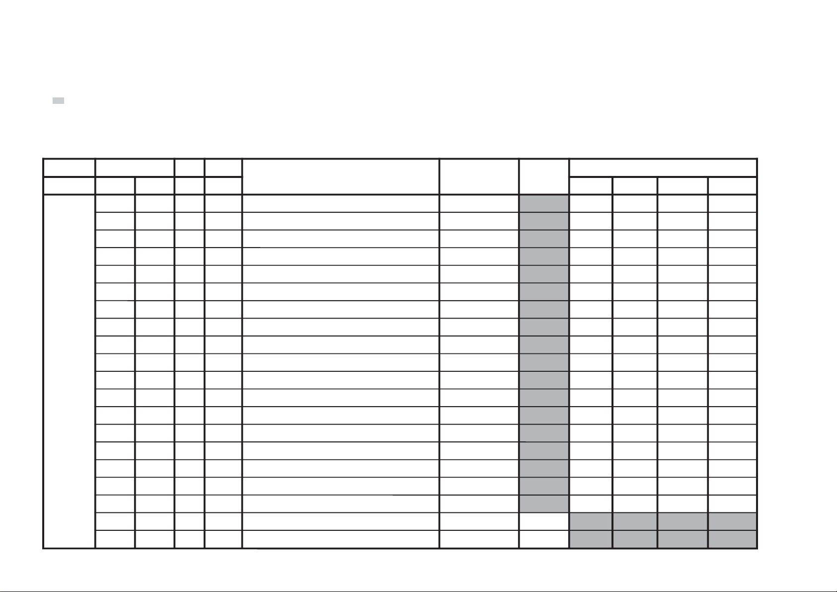
Adjustment Item Table
JVTytilanoitcnuF.tinIegnaRnoitcnuFemaNeciveDnommoC)deliateD(eulaVlaitinI
yrogetaC.oNemaNceDceD 05)3:4(06)3:4(05w)3:4(06w)3:4(
MOEG000SOPH130360)SH(tfihSlatnoziroHrossecorP-VT
62630373
100RAPH130360margolellaraPlatnoziroH
34442454
200WOBH130360woBlatnoziroH
03426282
300NILV130360ytiraeniLlacitreV
93939393
400RCSV130360llorcSlacitreV
13131313
500ZISH130360)WE(htdiWWE
24146474
600WPWE130360)WP(htdiW/alobaraPWE
54749453
700POCU710360alobaraPrenroCreppUWE
04839375
800POCL710360alobaraPrenroCrewoLWE
54748551
900ZTWE130360muizeparTWE
72718113
010PLSV130360)SV(epolSlacitreV
13131313
110ZISV510360edutilpmAlacitreV
12128191
210ROCS410360)CS(noitcerroC-S
73737373
310SOPV130360)HSV(tfihSlacitreV
84940444
410MOZV130360)ZV(mooZlacitreV
00000000
510LBH000100edoMgniknalBBGR
10101010
610FBW700510)FBW(gniknalBediWfognimiT
01300130
710RBW700510)RBW(gniknalBediWfognimiT
11011101
810LBS000100gniknalBecivreS00
910YPOC000100aeraMVNzH06/05llaotatadOEGehtypoCX
NOTE
a) In the initial value (detailed) column, the data after the slash mark ("/") refers to NTSC model data.
No ("/") means data is common for Multi and NTSC model.
b) Item remarked "*", please refer page 32 for the data.
c)
shaded items are no data.
d) Standard data listed on the Adjustment Item Tab le are reference values, therefore it may be different for each model and for each mode.
e) Note for the Different Data those are the standard data values written on the microprocessor. Therefore, the data values of the models are stored respectively in the memory.
In the case of a device replacement, adjustment by rewriting the data value is necessary for some items.
f) Multi ver8.21, NTSC ver8.21N.
KV-SZ252M50/M61/M81/N50/N60
RM-GA002
– 20 –
Page 22
– 21 –
JVTytilanoitcnuF.tinIegnaRnoitcnuFetoN&elbaTemaNeciveDnommoC )deliateD(eulaVlaitinI
yrogetaC.oNemaNceDceD
pmeTloC
LOOC(
)rehto
pmeTloC
MRAW(
)rehto
pmeTloC
LARTUEN(
)rehto
pmeTloC
)VUYLOOC(
pmeTloC
MRAW(
)VUY
pmeTloC
LARTUEN(
)VUY
VUYlap05
)N(
lap05
)oediV(
0edomciP
diviV/
1edomciP
dtS/
2edomciP
motsuC/
VToediV
LBHW000ROKB130360)10=BFO(BtesffO,)00=BFO(RtesffOleveLkcalB )srehtO/BGR/VU(*)lamroN/WOL/HGIH(pmetlocrossecorP-VT
131313131313
100GOKB130360GtesffOleveLkcalB )srehtO/BGR/VU(*)lamroN/WOL/HGIH(pmetloc
020202020202
200VRDR730360RtnioPetihW )srehtO/BGR/VU(*)lamroN/WOL/HGIH(pmetlocrossecorP-VT
737373737373
300VRDG730360GtnioPetihW )srehtO/BGR/VU(*)lamroN/WOL/HGIH(pmetloc
542473542473
400VRDB730360BtnioPetihW )srehtO/BGR/VU(*)lamroN/WOL/HGIH(pmetloc
340403340403
500GPL000100teserPniaGBGR enon00
600RGP130721)RGP(RniaGteserP enon95
700GGP130721)GGP(GniaGteserP enon95
800BGP130721)BGP(BniaGteserP enon95
900FONG000510tesffOniaGteserP enonpoolCCC01
010TRBS
130360ssenthgirB-buS nlaP*/)VT(nlaP*/)oediV(rehtO/VT(srehtO
]ylnosledomSU*[VUY/)oediV(
235333
5333
110ORBS000300)ciPtnegilletnI(tesffOssenthgirB-buS enon00
210SBC000100gnitimiLtnerruCmaeBfoecneuqeSlortnoC enon00
310BBGR000300gniknalBBGR enon
410GBLB000100tuptuOneerG&eulBfogniknalB enon00
510BFO000100eulBtesffOleveLkcalB enon10
610PBW000300)woL:3,2,lamroN:1,hgiH:0(gnitteSpmeTroloC edoMerutciP
001010
JVTytilanoitcnuF.tinIegnaRnoitcnuFetoN&elbaTemaNeciveDnommoC )deliateD(eulaVlaitinI
yrogetaC.oNemaNceDceD
VUYlap05
)VT(
lap05
)oediV(
maceS05
)VT(
maceS05
)oediV(
cstn06
)VT(
cstn06
)oediV(
VUY05VUY06/0edomciP
diviV
/1edomciP
dradnatS
/2edomciP
motsuC
VToediV
ediWVT
)3:4(
ediWoediV
)3:4(
JDAS000XAMP360360mumixaMerutciP >ediW/lamroN</)ediW/lamroN(*)oediV/VT(rossecorP-VT
84842424
100EUHS700510euH-buS oediV/VT
6011
200PHSS510360ssenprahS-buS VUY/oediV/VT
03
6243
300OHSS000700)ciPtnegilletnI(tesffOssenprahS-buS enon40
400LOCS130360roloC-buS /)oediv(maces05/)vt(maces05/)oediv(lap05/)vt(lap05
BGR06/BGR05/VUY06/VUY05/oediv06/VT06
5373921333131443
500OOCS000300)ciPtnegilletnI(tesffOroloC-buS enon20
600CIP130721;)dilavni(001>;)dilav(001~0:AG[lortnoCerutciP
])dilavni(6tiberongi;)dilav(36~0:srehtO
)ataDteseRresU=lanosreP:AG(ledoMerutciP
00117001
700LOC130721;)dilavni(001>;)dilav(001~0:AG[lortnoCroloC
])dilavni(6tiberongi;)dilav(36~0:srehtO
)ataDteseRresU=lanosreP:AG(ledoMerutciP
751405
800TRB130721;)dilavni(001>;)dilav(001~0:AG[lortnoCssenthgirB
])dilavni(6tiberongi;)dilav(36~0:srehtO
)ataDteseRresU=lanosreP:AG(ledoMerutciP
847405
900EUH130721;)dilavni(001>;)dilav(001~0:AG[lortnoCeuH
])dilavni(6tiberongi;)dilav(36~0:srehtO
)ledomSUhtiw)0-5(hE1#TNITotdneS*(
)ataDteseRresU=lanosreP:AG(ledoMerutciP
058405
010PHS130721;)dilavni(001>;)dilav(001~0:AG[lortnoCssenprahS
])dilavni(6tiberongi;)dilav(36~0:srehtO
)ataDteseRresU=lanosreP:AG(ledoMerutciP
850505
KV-SZ252M50/M61/M81/N50/N60
RM-GA002
Page 23
JVTytilanoitcnuF.tinIegnaRnoitcnuFetoN&elbaTemaNeciveDnommoC )deliateD(eulaVlaitinI
yrogetaC.oNemaNceDceD srehtOVUY)VT(LAP)VT(CSTN)VT(MACES)oediV(LAP)oediV(CSTN)oediV(MACESTUPNI-SMACESCSTNVT
CY000QRFP000300yaleDdnaycneuqerFretneCgnikaeP rehto/VTrossecorP-VT
00
00
100APR100300toohSrevO&erPoitaR rehto/VT
20
20
200OPR200300skaePevitageN&evitisoPfooitaR rehto/VT
20
20
300YLDY210510yaleD-Y TUPNI-S/VUY+)OEDIV/VT(*)MACES/CSTN/LAP(
** * * * * *
400TAMC000300xirtaM)ASU/napaJ(CSTNroMACES-LAP 00
500LCA100100gnitimiLroloCcitamotuA 10
600BC000100ycneuqerFretneCssapdnaBamorhC )xif0:oediV*(VThtiwylnodilav00
700OBS100300tesffOkcalBMACES 10
800ESHC100300ytivitisneStnedICSTN/LAP 20
900OLC000100retliF)lleB(ehcolCfoycneuqerFretneC 00
010PRTC000100edoMparTamorhC srehto/MACES
*
*
110TDQ000100parTamorhCdnoceS srehto/MACES
*
*
210SPB
000100eniLyaleDdnab-esaBamorhCfossapyB
srehto/CSTN
00
*
310OCF
000100nOroloCdecroF 00
410TNIT130360lortnoCtniTdnaB-esaB VT/srehto/VUY
2323
23
510VUT000100slangiSVUnolortnoCtniT 00
610CYWB000100
roloczH85.3rofedomCYtahtdiwdnaB
)CYWB(metsys
00
710BSO000100
amorhcfoeslupyektsrublanretnifohtdiW
)BSO(rotaludomed
00
810CKB000100noitisoPyektsruB
00
1000
JVTytilanoitcnuF.tinIegnaRnoitcnuFetoN&elbaTemaNeciveDnommoC)deliateD(eulaVlaitinI
yrogetaC.oNemaNceDceD 05)3:4(06)3:4(srehtOVUY)FFO_PI(VToediVtxeteleT)NO_PI(pi-VTlangisoN
CNYS000SYS000100tupnICNYSYnonoitazinorhcnyS 00
100OF000300tnatsnoCemiT1esahP )FR(langisoNrogninuTotuA/txeteleT/oediV/FFOPIVT/NOPIVT
3030100000
200DIV000100edoMtnedIoediV 06/05
0000
300LSF000100cnySlacitreVrofleveLgnicilSdecroF 00
400LSS000100rotarapeScnySleveLgnicilS 06/05
0000
500DIVS100700noitacifitnedIoediVrofnoitceleSecruoS srehtO/VUY
0000
600FROF000300ycneuqerFdleiFdecroF 30
700KVM000100gniyeKnoisiVorcaM 10
(For '*' refer to page 32)
– 22 –
KV-SZ252M50/M61/M81/N50/N60
RM-GA002
Page 24
– 23 –
JVTytilanoitcnuF.tinIegnaRnoitcnuFetoN&elbaTemaNeciveDnommoC )deliateD(eulaVlaitinI
yrogetaC.oNemaNceDceD
srehtOdiviVVT
)nyD(
VT
)srehtO(
oediV
)nyD(
oediV
)srehtO(
pmeTroloC
)HGIH(
pmeTroloC
)srehtO(
roloC
)WOL(pmeT
pmeTroloC
)LAMRON(
TCIP000LDAC700510leveLevirDedohtaC 30
100AFC000300edoMretliFbmoC *
200COS200300leveLgnippilCtfoS 00
300LWP100100hctiwSgnitimiLetihWkaeP 10
400LTHW600510gnitimiLetihWkaeP 20
500MAG100100ammaG 10
600STW100300hctertSetihWdnalortnoCammaGsrehtO/eviL
10/*10/*
700RFT000100langiSecnanimuLfooitaRrefsnarTCDsrehtO/eviL
1010
800ROC300300gniroC )srehto/anyD(*)oediV/VT(
10200010
900OROC000300)ciPtnegilletnI(tesffOgniroC 10
010SKB300300hctertSkcalBsrehto/BGR20
110SAA100100hctertSkcalBehtffohctiwSotaerAkcalB 10
210KSD000100lortnoCnikScimanyD 00
310SLB000100hctertSeulB )SREHTO/HGIH(pmetloc
0000
410SLBN000100tiucriChctertSeulBnoitarepO 00
510RRN000100noitcudeRdeRnoN )LAMRON/WOL/HGIH(pmetloc
10
1010
JVTytilanoitcnuF.tinIegnaRnoitcnuFetoN&elbaTemaNeciveDnommoC)deliateD(eulaVlaitinI
yrogetaC.oNemaNceDceD VUYVToediV
WS100OVS10030084@niPISBVC/OVS/OVFIfonoitcnuFVUY/oediV/VT
301010
KV-SZ252M50/M61/M81/N50/N60
RM-GA002
Page 25
– 24 –
JVTytilanoitcnuF
laitinI
egnaR
noitcnuFetoN&elbaTemaNeciveDnommoC
yrogetaC.oNemaNceDceD
FIV000DFIO630360rotaludomeDFItesffO rossecorP-VT63
100TCGA130360revo-ekaTCGA 81
200MTS000100edoMgninuThcraeS 10
300DG000100langiS1SBVCnoyaleDpuorG 00
400SCGA100300deepSCGAFI 10
500IFF000100LLPFIretliFtsaF 00
600IANL000100eulavlaitinitibANLpmAFR 00
700TANL591522leveLdlohserhTpmAFR 591
800NSNL400700dlohserhTleveLNSpmAFR 30
900DSNL200700dlohserhTporDleveLNSpmAFR 10
010XENL610360gnimiTporDNSkcehcpmAFR 03
110RTHC840721edoMresUpmAFRtesotgrPotuAretfadlohserhTlennahC 52
210OSUT000100desUrenuTynoS *
JVTytilanoitcnuF.tinIegnaRnoitcnuFetoN&elbaTemaNeciveDnommoC)deliateD(eulaVlaitinI
yrogetaC.oNemaNceDceD
srehtO/0edomciP
diviV
/1edomciP
dradnatS
/2edomciP
motsuC
VT
MV000DBGR300700tuptuOMVottuptuOBGRfoyaleDenonrossecorP-VT30
100AMV300300tuptuOMVfoedutilpmAenon30
200PAMV200300)FFO:3,2,woL:1,hgiH:0(gnittesMVedoMerutciP
000000
300OMMV300300edoMMV 30
400AMVF
400400)erawtfoSlluF(tuptuOMVfoedutilpmA
srehto/MACES
500OARC000100MVSnogniroCsrehto/VT
00
10
KV-SZ252M50/M61/M81/N50/N60
RM-GA002
(For '*' refer to page 32)
Page 26
JVTytilanoitcnuF.tinIegnaRnoitcnuFetoN&elbaTemaNeciveDnommoC
yrogetaC.oNemaNceDceD
MEDS000SWMF000300rotaludomeDMFrofnoitceleSwodniW rossecorP-VT20
100SSQ100100 )metsysMitlumAGrofA/N(edoMreifilpmA)SSQ(dnuoStilpSisauQ 10/*
200BPB000100retliFssapdnaBdnuoSfossapyB 00
300OLMA000100dnuoSMAroflangiStuptuOoiduA 00
400CVPH000100lortnoCemuloVenohPdaeH 00
500ACMC000100lennahConoMetavitcA 00
600SBPB000100)SBPB(edomoeretstaretlifssapdnabdnuosfossapyB 10
JVTytilanoitcnuF.tinIegnaRnoitcnuFetoN&elbaTemaNeciveDnommoC
yrogetaC.oNemaNceDceD
TXT000VXT930360spilihProfnoitisoPlacitreVtxeteleT redoceDtxeT93
100DHT010721tfihSegdEevitcAcnys-HtxeteleT 01
200RBT510130ssenthgirBBGRtxeteleT 81
300QCA000100)1-LAP,0-otuA(noitisiuqcAtxeteleT RFS10
400MRBT300130ssenthgirBedoMxiMtxeteleT 30
(For '*' refer to page 32)
– 25 –
KV-SZ252M50/M61/M81/N50/N60
RM-GA002
Page 27
JVTytilanoitcnuF.tinIegnaRnoitcnuFetoN&elbaTemaNeciveDnommoC )deliateD(eulaVlaitinI
yrogetaC.oNemaNceDceD VToediV
ffOdnuorruS
)WOW/SRS(
dnuorruS
)dnuorrusurT(
dnuorruS
)no(oeretsI(
)eivoM/
dnuorruS
)detalumiS(onomI(
)tropS/
dnuorruS
,SRS:rehtO(
)ffO,oeretsI
PSDS000LBB000510ruotnoCEBB rehto/wow/urT>ylnolluF-LIXBDSS
0000
0000
100HBB000510ssecorPEBB rehto/wow/urT>ylnolluF-LIXB
0000
0000
200WLBB000510tesffOruotnoCEBB 40
300FOVS000510tesffOemuloVedoMtceffE/dnuorruS onomI/oeretsI/dnuorrusurT/)WOW/SRS(ffO
6011608060
400DAL000130tsujdAleveLredoceD
50
500MAL000130tsujdAleveLonoM 50
600NAL000130tsujdAleveLmaciN 22
700SAL000130tsujdAleveLPAS 50
800AAL000130tsujdAleveLCDA buSoediV/buSFR/kpSretnec/oediV/FR
0000
900FES300700tceffEoeretS/onoMelbidercnI onomI/oeretsI
5030
010SAB000130)evitageN:1evitisoP:0BSM(tesffOssaBniaM
2222
2222
110ERT000130)evitageN:1evitisoP:0BSM(tesffOelberTniaM
7272
7272
2101QE000130tesffO)zH001(dnaBlennahCniaMrezilauqE
)evitageN:1evitisoP:0BSM(
1010
1010
3102QE000130tesffO)zH003(dnaBlennahCniaMrezilauqE
)evitageN:1evitisoP:0BSM(
8181
8181
4103QE000130tesffO)zH0001(dnaBlennahCniaMrezilauqE
)evitageN:1evitisoP:0BSM(
1010
1010
5104QE000130tesffO)zH0003(dnaBlennahCniaMrezilauqE
)evitageN:1evitisoP:0BSM(
6161
6160
6105QE000130tesffO)zH0008(dnaBlennahCniaMrezilauqE
)evitageN:1evitisoP:0BSM(
1010
1010
710TCFB500700lortnoCEBBdnaBUD,EBD 00
810NECS100510lortnoCretneCD3SRS 40
910APSS000510lortnoCecapSD3SRS 10
020WHBB000510edomWOWnitesffossecorpEBB 00
120ERTS200700edomdnuorrusroftesffOelberT 10
220THBB000510edomVTnitesffOEBB 00
320ERTT200700edomVTnitesffOelberT 30
420SABV000300emulovresunodnepedtesffossaB 10
520ERTV000300emulovresunodnepedtesffoelberT 10
620SABT200700VTroftesffossaB 00
720OLBB000300emuloVresUnodnepedtesffOLBB 00
820OHBB000300emuloVresUnodnepedtesffOHBB 00
– 26 –
KV-SZ252M50/M61/M81/N50/N60
RM-GA002
Page 28
– 27 –
JVTytilanoitcnuF.tinIegnaRnoitcnuFetoN&elbaTemaNeciveDnommoC
yrogetaC.oNemaN
ceDceD
CEDS000UTPS300510noitcetedreirracPASrofdlohserhTreppU DSS80
100LTPS600510noitcetedreirracPASrofdlohserhTrewoL 51
200HTPS000130PASfoetumotuarofdlohserhTesioN 00
300YHPS400510PASfoetumotuarofezissiseretsyH 30
400HTMF000130dradnats2AMFni2CSfoetumotuarofdlohserhTesioN 81
500YHMF400510dradnats2AMFni2CSfoetumotuarofezissiseretsyH 70
600ELIN001552)PEDD(timilrorrerewolMACIN 05
700EUIN002552)PEDD(timilrorrereppuMACIN 002
800DMPE
100300
)PEDD(gnimmargorPysaECEDMED
0=DMPEfI
0=SDTSdna
tiB3POdna
CEDS1=1
siyrogetac
dnaelbasiD
yrogetacCKDS
revoekatlliw
10/*
900SDTS
910130
sedomSSSdnaDSArofdexelpitlumstiB
31/*
010AMVO100100noitpadanoitaludomrevoMF 00
110WBLF000300htdiwdnabretlifrotaludomedMA/MF 30
210DMDI000300edomSSSnideepstnediMF 00
310TMVO100200lanimonotevitalerdlohserhtlevelnoitaludomrevO 30
410IXCD000100retrevnIlortnoCgnilacSOXCDMACIN 00/*
510GXCD000700niaGlortnoCgnilacSOXCDMACIN 00/*
610LLCD110510)L(timiLlortnoCgnilacSOXCDMACIN 00
710HLCD000130)H(timiLlortnoCgnilacSOXCDMACIN 00/*
810RKDI100300DTSMnaeroKgnittesDOMDI 00
JVTytilanoitcnuF.tinIegnaRnoitcnuF etoN&elbaTemaNeciveDnommoC
yrogetaC.oNemaNceDceD
CKDS000LLNK000552etyBrewoLdlohserhTrewoLteDesioNnaeroK 0=DMPEfI
0=SDTSdna
CKDSdnaelbasiDsiyrogetacCEDS1=1tiB3POdna
revoekatlliwyrogetac
100HLNK
210552etyBrehgiHdlohserhTrewoLteDesioNnaeroK
200LHNK000552etyBrewoLdlohserhTreppUteDesioNnaeroK
300HHNK020552etyBrehgiHdlohserhTreppUteDesioNnaeroK
400CILK060552tnuoCgniniatniaMDItoliPtsoLnaeroK
500MILK100721reilpitluMtnuoCgniniatniaMDItoliPtsoLnaeroK
600CDSK600552tnuoCtceteDoeretSnaeroK
(For '*' refer to page 32)
KV-SZ252M50/M61/M81/N50/N60
RM-GA002
Page 29
KV-SZ252M50/M61/M81/N50/N60
JVTytilanoitcnuF
.tinIegnaRnoitcnuFetoN&elbaTemaNeciveDnommoC )deliateD(eulaVlaitinI
yrogetaC.oNemaN
ceDceD 05)3.4(06)3:4(ZW05)9:61(ZW06)9:61(N05)9:61(N06)9:61(F05)9:61(F06)9:61(Z05)9:61(Z06)9:61(zH05buSzH06buSVToediV
PIP
000SPH
150552noitisoPerutciPlatnoziroH X8829ADS
100SPV
720552noitisoPerutciPlacitreV
200PFV
800510noitisoPeniFlacitreV
300PFH
510510noitisoPeniFlatnoziroH
)ciPbuS(zH06/05
400PSV
000100noitcudeResioNesluPcnySlacitreV
500LDV
000130yaleDesluPcnySlacitreV
600YLD
100510yaleDyaleS
700VGA
110510eulaVlortnoCniaGcitamotuA
800DPC
000300noitaruDgnipmalC
900LLP
000300tnatsnoCemitLLPtresnI
oediV/VT
010DCY
210510yaleDC/Y
110LIK
000300dlohserhTrellikroloC
210PGB
000100noitisoPetaGtsruB
310MED
100300noitcleSesahpmeeD
410AMC100300hctiwdnaBamorhC
510CFI
200300retliFnoitasnepmoCFI
610EUH
230360lortnoCEUH
710ACS
600130tnemtsujdAreirracbuSroloC
810NOC
000510tnemtsujdAtsartnoC
910TRB
000510tnemtsujdAssenthgirb
020RKP
331552deRleveLkaeP
120GKP
331552neerGleveLkaeP
220BKP
331552eulBleveLkaeP
320YRF
510510YroloCemarF
420TAS
700510tnemtsujdAnoitarutaSroloC
520KPY
300700tnemtsujdAgnikaePY
620OCY
100100elbanEgniroCY
72012P
0007001LDILAPdna2LDILAP
820LAP
000100leveLDILAP
920VOP
000700lacitreVtesffOnoitisoP
030HOP
610130latnoziroHtesffOnoitisoP
130LPC
100300htgneLesluPgnipmalC
230LRS
000300leveLnoitcejeRmaceS
330LIS
700700leveLnoitakifitnedImaceS
430DES
100100redividmaceS
530AFB
100100tnemtsujdAretliflleB
63021P
0003002dna1tnemercnILAP
730SOL
100300deepSgnikcoL
oediV/VT
830LAS
000700leveLecnatpeccAmaceS
930AES
000100ecnatpeccAmaceS
040RSN
000700LLPlatnoziroHroFnoitcudeResioN
oediV/VT
140HLS
000300HdlohserhTleveLgnicilS
240JAI
000300LLPlatnoziroHroFtnemtsujda-I
34005V
000721zH05gninepOnoisserppuSesioNwodniWlacitreV
44006V
230721zH06gninepOnoisserppuSesioNwodniWlacitreV
540SNV
000510zH06gnisolCnoisserppuSesioNwodniWlacitreV
640CSV
000510zH05gnisolCnoisserppuSesioNwodniWlacitreV
740TVS
510510VTLS&ytiraloPVdlohserhTleveLgnicilS
840MFV
000300edoMleehwylFlacitreV
940WFV
000100leehwylFlacitreV
050SVL
000300noitarapes-cnySlacitreVrofssapwoL
150ALC
300300ycnetalgnipmalC
250PCS
400130esluPgnipmalCfotratS
– 28 –
(Not used for this model)
RM-GA002
Page 30
JVTytilanoitcnuF.tinIegnaRnoitcnuFetoN&elbaTemaNeciveDnommoC
yrogetaC.oNemaNceDceD
VTH000XAMV000360)XAMV+53=XAM(leveLemuloVmumixaM leveLemuloV00
100INIV520130norewoPtaleveLemuloVlaitinI leveLemuloV00
200YBTS000100 )YBTSsyawla=1,sutatsrewoptsalehtwollof=0(sutatSrewoPtsaL rewoPtsaL00
300GRPI100721)sledoMitluMrofylno(norewoPtarebmuNmargorPlaitinI rebmuNmargorP00
JVTytilanoitcnuF.tinIegnaRnoitcnuFetoN&elbaTemaNeciveDnommoC)deliateD(eulaVlaitinI
yrogetaC.oNemaNceDceD 05)3:4(06)3:4(srehtOVUY
MTPO000THSA600700)nim5*atad(remitffotuhsotuA 70/00
100BDSO510130ssenthgirbDSO h06orciM/RMM61
200HDSO800510noitisoPlatnoziroHDSO h06orciM/ATADX80
300VDSO730360noitisoPlacitreVDSO
)06/05(9:61<>06/053:4<
>)lluFlamroN()mooZediW()ediW(
h06orciM/RMM
1623
400ETUM000100)delbane=1(hctiwSetuMlangiSoN 10/00
500LUFR510510)hf0nehwelbasiD(dekcolnUretfaretnuoCegnahClangiSFR 10/40
600KLFR510510)hf0nehwelbasiD(dekcoLretfaretnuoCegnahClangiSFR 40/00
700GNAL000300noitidnocgnippihsegaugnalDSO 00
800TXTH000100wsrotarepescnyS srehto/VUYrossecorP-VT
0000
900SSMC000100wscnyS rossecorP-VT10
010OXCD060721eulaVOXCD PSD/h06orciM/RFS35/*
110CSID821552cedrolocybtsujdaOXCDrofatadOCSIDtegrat 821
210LBXE000510esioNetihWetanimilEotremiTgniknalBdednetxE 40/80
310SYST000300 )ledoMAG(]M:3,K/D:2,I:1,G/B:0[teseRtseTtaMVNnisySVTeziromeM 00
410WSNL100100)ffO:0,otuA:1(noitidnocteseRtseT/gnippihSretsooBlangiS 10
510LBL100100noitidnoclangiSoNtAnoitcudeRssenthgirB 10
610ORPH100100noitatoRerutciProftesffOarapH 50
710LUVA510510)hF0nehwelbasiD(dekcolnUretfaretnuocegnahclangisvA 40
810KLVA510510)hF0nehwelbasiD()dekcolretfaretnuocegnahclangisvA -/00
910MPSC000100 )edompotselbasid:1,edompots:0(ybdnatsniedompotselbasiD 10
020HNES000100)nO:1,ffO:0(m/cdnuosgnilkcarCrecnahnEdnuoS 10
120CSPS100300)semit8:3,semit6:2,semit4:1,elbasid:0(hcraeSDEEPS 10
220OLUM100100)woLevitcA:1,hgiHevitcA:0(noitceleScigoLtroPetuMoiduA 10
– 29 –
(For '*' refer to page 32)
KV-SZ252M50/M61/M81/N50/N60
RM-GA002
Page 31

JVTytilanoitcnuF.tinIegnaRnoitcnuFetoN&elbaTemaNeciveDnommoC
yrogetaC.oNemaNceDceD
MFPO000TCMF100300dlohserhTreirraCnacSotuAoidaRMF 02
100TSPR300721teserpoidargnirudpetsycneuqerfhcaerofemitgnitiaW 01
200UTPM300510)OIDARMF(noitcetedtolipXPMrofdlohserhTreppU DSS21
300UOCD331552rotaludomedMFmorftesffoCDrofdlohserhTreppU 241/*
400LOCD711552rotaludomedMFmorftesffoCDrofdlohserhTrewoL 611/*
500AMVO100100)OIDARMF(noitpadanoitaludomrevoMF DSS00
600RBMF000130edoMMFgnirudssenthgirBDSO h06orciM/RMM11
700ERTR000700edoMoidaRMFnitesffOelberT DSS20
800SABR200800edoMoidaRMFnitesffOssaB DSS20
900TCGA540360edoMoidaRMFnirevoekatGCA rossecorP-VT*
010WBLF300300htdiwdnabretlifrotaludomedMA/MF DSS10
110SDTS000100
sisahpmeedsu05)71(LESDTS:OFIelbatceleS
)ylnoCSTN/SU(sisahpmeedsu57)81(LESDTS:1
00
JVTytilanoitcnuF.tinIegnaRnoitcnuFetoN&elbaTemaNeciveDnommoC)deliateD(eulaVlaitinI
yrogetaC.oNemaNceDceD srehtOVUY
SUPO000FFOS000100)noCAhtiwybdnats:1,noCAhtiwyromemtsalwollof:0(ffoyatS 00/-
100HCPS100721noitidnoCgnippihSretfarebmuNlennahC 70/-
200ACPS100100)nOelbaC=1(noitidnoCgnippihSretfanoitceleSelbaC 10/-
300RBCC510130)SUrofylno(ssenthgirBCC 00/-
400PHCC800510)SUrofylno(noitisoPHCC 00/-
500VUO000100)SUrofylno(slangiStupniVUnolortnoCtesffO VUY/srehtO
00/-00/-
6002AFC
000100
)SUrofylno(nOretliFbmoCdecroF enon
00/-
700CYSH000700SUrofylno)DISrokcoL,LS(gninnutrofnoitcelescnySH 00/-
800KLC521552SUrofylno)nim51/sm8:pets1(tesffokcolcSU 00/-
900SKLC521552SUrofylno)nim51/sm8:pets1(ybdnatsnitesffokcolcSU 00/-
(For NTSC model only)
– 30 –
KV-SZ252M50/M61/M81/N50/N60
RM-GA002
(For '*' refer to page 32)
Page 32

– 31 –
JVTytilanoitcnuF.tinIegnaRnoitcnuFetoN&elbaTemaNeciveDnommoC
yrogetaC.oNemaNceDceD
BTPO000LLAI000100)MVNnideziromemton(hctiwSetirWdradnatS x
1001BPO000552)detalermetsyS(1noitpO 33egaprefer
2002BPO000552)detalerlangiSoediV(2noitpO 33egaprefer
3003BPO000552)detalergnidoceDoeretS(3noitpO 43egaprefer
4004BPO000552)suoenallecsiM(4noitpO 43egaprefer
5005BPO000552)suoenallecsiM(5noitpO 53egaprefer
6006BPO000552)detaleregaugnaLDSO(6noitpO 53egaprefer
KV-SZ252M50/M61/M81/N50/N60
RM-GA002
Page 33

KV-SZ252M50/M61/M81/N50/N60
RM-GA002
Data Variant depend on models
Category No Name Table Comb No Comb
YC 003 YDLY YUV 10 10
010 CTRP Other 00 01
011 QDT Other 00 01
012 BPS NTSC 01 00
Category No Name Comb No Comb
PICT 001 CFA 00 01
PAL (TV) 10 06
NTSC (TV) 10 03
SECAM (TV) 06 06
PAL (Video) 11 03
NTSC (Video) 09 06
SECAM (Video) 06 03
SECAM 01 01
SECAM 00 00
Category No Name Others Live/Vivid
PICT 006 WTS Comb 01 01
No Comb 01 02
Category No Name Sony Tuner Current Alps Tuner New VA Alps (TEQEXL01A) Panasonic Tuner
VIF 012 TUSO 01 00 02 03
Category No Name Stereo AV Stereo India/ China Vietnam
SDEM 001 QSS 01 00 01 01
Category No Name Stereo AV Stereo
SDEC 008 EPMD 02 01
009 STDS 31 13
014 DCXI 00 00
015 DCXG 03 00
017 DCLH 06 00
Category No Name Stereo AV Stereo Mono
OPTM 010 DCXO 54 53 53
Category No Name Sony Tuner Alps Tuner Pana Tuner
OPFM 003 DCOU 140 144 142
004 DCOL 114 118 116
OPFM 009 AGCT = VIF 01 AGCT (A87F) + Offset
15 2 2
– 32 –
Page 34

KV-SZ252M50/M61/M81/N50/N60
RM-GA002
ITEM INFORMATION
No. OPB1
Item
KV-SZ252M50 000 0111115
KV-SZ252M61 000 0111115
KV-SZ252M81 000 0111115
KV-SZ252N50 000 010008
KV-SZ252N60 000 010008
Reserved Mini Visualizer M B/G I D/K DEC
Jack
00 =
01 =
10 =
11 = 1 =
Mini Jack (US MODEL only) 0 = disabled, 1 = enabled
Visualizer (BX1L FULL only) 0 = disabled, 1 = enabled
TV System Select (M, B/G, I, D/K) 0 = disabled, 1 = enabled
No. OPB2
Item
KV-SZ252M50 001 0110044
KV-SZ252M61 011 01100108
KV-SZ252M81 001 0110044
KV-SZ252N50 001 0110044
KV-SZ252N60 011 01100108
Party Mode FM Radio Component Composite (SCART) SECAM Color Decording DEC
Party Mode Party Mode Function 0 = not available, 1 = available
FM Radio FM Radio Function 0 = not available, 1 = available
Component (Component [YCbCr] Terminals) 0 = not available, 1 = available
Composite (No. of Composite Terminals) 00 = 1 composite terminal
01 = 2 composite terminals
10 = 3 composite terminals
11 = 4 composite terminals
SECAM (SECAM Color System) 0 = disabled, 1 = enabled
Color decoding (Color Crystal Selection) 00 = PAL/NTSC (Multi)
01 = NTSC (3.58MHz)
10 = PAL/NTSC (4.43MHz)
11 = PAL/NTSC (Tri-Norma)
– 33 –
Page 35

KV-SZ252M50/M61/M81/N50/N60
RM-GA002
No. OPB3
Item
KV-SZ252M50 000 000011
KV-SZ252M61 011 10000112
KV-SZ252M81 000 000011
KV-SZ252N50 000 000011
KV-SZ252N60 000 001004
Reserved NICAM NICAM A2 ST Thai US ST JP/Korean MONO DEC
Reserved Not used
NICAM ST (NICAM Stereo) 0 = disabled, 1 = enabled
NICAM BI (NICAM Bilingual) 0 = disabled, 1 = enabled
A2 ST/BI (A2 [West German]
Thai Bilingual (A2 [Thai] Bilingual)
US ST (US Stereo) 0 = disabled, 1 = enabled
Korean ST (Korean Stereo) 0 = disabled, 1 = enabled
MONO (Monaural Model) 0 = Stereo (SSD) Model
ST BI Bilingual ST
Stereo/Bilingual) 0 = disabled, 1 = enabled
or Force SAP if US ST is active 0 = disabled, 1 = enabled
1 = Monaural Model
No. OPB4
Item
KV-SZ252M50 001 0110044
KV-SZ252M61 001 0000133
KV-SZ252M81 001 0110145
KV-SZ252N50 001 0110044
KV-SZ252N60 001 0000032
Initial setup 1 spk VM Surround Top Text DEC
menu Models
Initial Setup menu Skip Initial Setup
"Display this menu next time?" 0 = Not Skip, 1= Skip Initial Setup "Display this menu
(for us models or)
1 spk Models 1 Speaker Models 0 = 2 or 3 Speaker Models, 1 = 1 speaker Models
VM (Velocity Modulation) 0 = disabled, 1 = enabled
Surround (Surround Selection) 000 = Off/Simulated/Surround
001 = Off/Simulated/SRS (3D) Surround
010 = Off/Simulated/WOW/TruSurround
011 = No Surround
100 = Off/Sports/Movie
101 = Off/Sports/Tru Surround
110 = 3.1 Channel Surround Off/Sim/Tru
(US models only)
111 = 5.1 Channel Surround Off/5.1/Sim/Tru
(US models only)
TOP(Forced TOP) 0 = Auto Mode (TOP/FLOF), 1 = Forced TOP
TEXT (Teletext Model) 0 = Non-Teletext Model, 1 = Teletext Model
– 34 –
Page 36

KV-SZ252M50/M61/M81/N50/N60
RM-GA002
No. OPB5
Item
KV-SZ252M50 101 01011171
KV-SZ252M61 100 11011155
KV-SZ252M81 101 01011171
KV-SZ252N50 000 0101111
KV-SZ252N60 000 0101111
Signal MSYS COSMIC_A ASD Tilt Band IP Wide DEC
Booster ASD ASD Edge
Signal Booster Signal Booster feature 0 = disabled, 1 = enabled
MSYS ASD (ASD Improvement for 0 = disabled, 1 = enabled
M System channels)
*Only applicable when ASD = 1
COSMIC ASD Automatic Standard Detection 0 = disabled, 1 = enabled
Using COSMIC (Non-Stereo)
ASD (Automatic Standard Detection) 0 = disabled, 1 = enabled
Tilt (Tilt Correction/PIC Rotation) 0 = disabled, 1 = enabled
Band Edge (VHF-H band Limit Position) 0 = 427.25MHz, 1 = 429.25MHz
IP Plus (Intelligent Picture & 0 = disabled, 1 = enabled
Intelligent Picture Plus)
Wide (Wide Mode/V-Compressed) 0 = disabled, 1 = enabled
No. OPB6
Item
KV-SZ252M50 100 01000136
KV-SZ252M61 000 010008
KV-SZ252M81 100 00100132
KV-SZ252N50 100 01010138
KV-SZ252N60 000 0101010
AV ST Mono 3D OSD 3D Comb PiP OSD Language Selection DEC
AVST Mono
3D OSD (BX1L Full version GA Multi 0 = Normal with 3D Intelligent Picture OSD
3D Comb 3D comb feature 0 = Comb Not available
PiP PiP feature 0 = PiP Not Available
OSD Language Selection US (GA NTSC) 1x1x = Complicated Chinese
(AV Stereo mono Chip model) 0 = mono model
1 = AV stereo model
Destination ONLY) 1 = Disable 3D Intelligent picture OSD
1 = Comb available
1 = PiP available
GA 1xxx = Simplified Chinese
x1xx = Arabic/Russian
x1xx = Arabic/Russian
xx1x = Thai
xxx1 = Persian/Vietnamese
– 35 –
Page 37

KV-SZ252M50/M61/M81/N50/N60
RM-GA002
4-3. PICTURE QUALITY ADJUSTMENT
4-3-1. P MAX / CONTRAST ADJUSTMENT
1. Set TV to Video mode.
2. Set Picture mode to "CUSTOM".
3. Input PAL 100% Color Bar to TV set (OTHER model)
and NTSC 75% Color Bar (NTSC model).
4. Set the following condition:
Picture 100%, Color 0%, Brightness 50%.
5. Connect an oscilloscope to pin 4 (R output) of CN004.
6. Go to service mode and set PICT 003 "PWL" to 00h and
WHBL 014 "BLBG" to 01h.
7. Select SADJ 000 "PMAX" with 1 and 4 button of the
commander then adjust VR with spec with 3 and 6
button until reach the spec below:
VR
Black
PAL
34"
VR
29"
25"
NTCS
1.85 0.03Vpp
1.57 0.03Vpp
1.85 0.03Vpp
8. Copy "SCOL" 50(PAL) video data to "SCOL" 50
(SECAM) video.
9. Then copy "SCOL" 50(PAL) video data and "SCOL"
50(SECAM) video data to "SCOL" 50(PAL) and "SCOL"
50(SECAM) TV table.
10. For NTSC model input NTSC 75% Color Bar to TV and
repeat step no. 4 to 6.
11. Select SADJ 004 "SCOL" with 1 and 4 button of the
commander then adjust using 3 and 6 so that
VB1=VB4 then write in the data as below:
Add 11 steps to SCOL (NTSC) – 25"
Add 11 steps to SCOL (NTSC) – 29"
Add 6 steps to SCOL (NTSC) – 34"
VB1 VB2 VB3
VB1 = VB4 (for NTSC)
(Difference is within 70mV)
VB4
12. Copy "SCOL" 60(NTSC) video data to "SCOL"
60(NTSC) TV .
13. Finally copy "SCOL" 50(PAL) and "SCOL" 60(NTSC)
data to "SCOL" 50(PAL) and 60(NTSC) in DVD mode.
14. Then press [MUTING] t - to write the data.
15. Set PICT 006 "WTS" back to original data.
Add 5 steps to "PMAX" - (25" and 29")
8. Then copy the adjusted PMAX data to TV mode.
9. Select Wide mode to "ON" in TV and Video mode and
write "PMAX" data -6 steps
(for models with V-Compression features only).
10. Press [MUTING] t - to write the data.
11. Set “PWL" and "BLBG" back to initial data.
("PWL" : 01h and "BLBG" : 00h).
12. Finally press [MUTING] t - to write the data.
4-3-2. SUB COLOR ADJUSTMENT
1. Set TV to Video mode.
2. Set Picture mode to "CUSTOM".
3. Input PAL 100% Color Bar to TV.
4. Set the following condition:
Picture 100%, Color 50%, Brightness 50%, Hue 50%
and Sharpness 50%
5. Set PICT 006 "WTS" to 00h.
6. Connect an oscilloscope to pin 2 (B output) of CN004 A
Board.
7. Select SADJ 004 "SCOL" with 1 and 4 button of the
commander then adjust with 3 and 6 so that
VB2=VB3=VB4 (for PAL) then write in the data as below:
Add 11 steps to "SCOL" (PAL) – 25"
Add 11 steps to vSCOL" (PAL) – 29"
Add 6 steps to "SCOL" (PAL) – 34"
VB1
4-3-3.SUB HUE ADJUSTMENT
1. Set TV to Video mode.
2. Input NTSC 3.58 Color Bar to TV set.
3. Set the following condition:
Picture 100%, Color 50%, Brightness 50%, Hue 50%,
Sharpness 50%.
4. Connect oscilloscope to pin 2 (B output) of CN004.
5. Set to service mode and select SADJ 001 "SHUE" or
YC 013 "TINT" with 1 and 4 button then adjust to
VB1=VB2=VB3=VB4 using 3 and 6 button.
6. Press [MUTING] t - to write the data.
7. Select TV channel with NTSC 3.58 and perform step 3
to 6.
8. For single system model with NTSC 4.43, select TV
channel with NTSC 4.43 and perform step 3 to 6.
9. Once adjustment is completed in Video mode, carry out
adjustment in DVD mode. Input NTSC 3.58 Color Bar.
10. Connect oscilloscope to pin 2 (B output) of CN004.
11. Set to service mode and adjust service item YC 013
"TINT" with 1 and 4 button until VB1=VB2=VB3=VB4.
12. Press [MUTING] t - to write the data.
VB3
VB1
VB2
Illustration 1
VB4
80mV
VB2 VB3 VB4
VB2 = VB3 = VB4 (for PAL)
The highest level of VB1, VB2, VB3 and VB4 should
be aligned at the same line.
The ideal difference between VB2 and VB3 is within
– 36 –
+ 80mV.
Page 38

KV-SZ252M50/M61/M81/N50/N60
RM-GA002
4-4. GEOMETRY ADJUSTMENT
4-4-1. H-TRAPEZOID ADJUSTMENT
1. Receive cross hatch/dot signal.
2. Adjust RV1800 on CV Board to make H-Trapezoid
distortion best/to obtain the center illustration shown in
Ta ble 1.
4-4-2. NORMAL MODE 50Hz / 60Hz
1. Input PAL Special Color Bar (SPCB) or PAL Monoscope
(OTHER model) and Video mode or NTSC Monoscope
(NTSC model) signal using a pattern generator.
2. Set Wide Mode to "OFF".
3. Select Category items listed in Table 1.
4. Raise and Lower the data value using 3 and 6 button
to obtain the center illustration.
5. Press [MUTING] t - to save the data into the memory.
6. For Korea models, copy adjusted 60Hz to 50Hz. Add 6
steps to 50Hz "HPOS" and 3 steps to 50Hz "HSIZ" and
save the data.
4-4-3. WIDE MODE 50Hz / 60Hz
(V Compression Adjustment)
1. Input PAL Special Color Bar (SPCB) (OTHER model) or
Monoscope NTSC (NTSC model) signal using a pattern
generator.
2. Set Wide Mode to "ON".
3. Copy NORMAL MODE 50Hz/60Hz adjusted data for the
following items:GEOM: 011 VSIZ, 010 VSLP, 012 SCOR and 003 VLIN
4. Select Category items listed in Table 1 except GEOM:
003 VLIN, 010 VSLP, 011 VSIZ, and 012 SCOR and
adjust the data to obtain the center illustration.
5. Press [MUTING] t - to save the data into the memory.
6. For Korea models, copy adjusted 60Hz to 50Hz. Add 6
steps to 50Hz "HPOS" and save the data.
Category Function Illustration
GEOM 000 H Position
(HPOS)
GEOM 001 H Parallelogram
(HPAR)
GEOM 002 H Bow
(HBOW)
GEOM 003 Linearity
(VLIN)
GEOM 005 EW Width
(HSIZ)
Note: Adjust HSIZ
16.6 + -(SPCB) _ 50Hz
14.8 + -(PAL Monoscope) _ 50Hz
15.3 + -(NTSC Monoscope) _ 60Hz
GEOM 006 EW Parabola/Width
(EWPW)
GEOM 007 EW Upper Corner
(UCOP) Parabola
GEOM 008 EW Lower Corner
(LCOP) Parabola
GEOM 009 EW Trapezoid
(EWTZ)
GEOM 011 V-Amplitude
(VSIZ)
Note: Adjust VSIZ
12.6 + -(SPCB) _ 50Hz
11.3 + -(PAL Monoscope) _ 50Hz
11.7 + -(NTSC Monoscope) _ 60Hz
GEOM 012 S-Correction
(SCOR)
GEOM 013 V-Shift
(VPOS)
Tabl e 1
– 37 –
Page 39

VIF
SAW
SIF
SAW
MAIN
Power
Supply
Stdby
Power
TUNER
Y
U
V
24.576MHz
Rear YUV in
Rear AV in
Front AV in
Mon out
* FM Radio Function (STEREO model)
Mon
out
AV1
in
AV2
in
YUV
in
AC in ~
110 ~ 220V
CISPR/
PFC
Relay
LOW B
Stdy 3.3
AUDIO VCC
L
Audio Amp
ATT
NVM
V Def
H Def
DF
DQP
VM
RGB Amp
Rot Amp
LCC Amp
6W
R
6W
L,R
H
P
EW, Hd
L,R
V+, V-
PWM
RGB
SIRCS
KEY
buttons
PLL
I/O Port
I/O Port
VIF & SIF
POWER
Color
Decoder
YUV
Processor
Jungle
RGB
A
D
C
D
A
C
Stereo,
DSP
Micro
Text
CC & V-chip
LED
+B
KV-SZ252M50/M61/M81/N50/N60
5-1. BLOCK DIAGRAM
RM-GA002
– 38 –
DIAGRAMS
SECTION 5
Page 40

5-2. CIRCUIT BOARDS LOCATION
CV Board
KV-SZ252M50/M61/M81/N50/N60
RM-GA002
A Board
5-3. SCHEMATIC DIAGRAM INFORMATION
Note:
• All capacitors are in µF unless otherwise noted.
• All electrolytic capacitors are rated at 50V unless otherwise
noted.
• All resistors are in ohms.
kΩ = 1000Ω, MΩ = 1000kΩ
• Indication of resistance which does not have rating electrical
power is as follows.
Pitch: 5 mm
Rating electrical power 1/4W (CHIP: 1/10W)
• : nonflammable resistor.
• : fusible resistor.
• ¢ : internal component.
•: panel designation or adjustment for repair.
• All variable and adjustable resistors have characteristic curve
B unless otherwise noted.
• Readings are taken with a color-bar signal input.
no mark : Common
(): PAL
[]: NTSC 3.58
• Readings are taken with a 10MΩ digital multimeter.
•Voltage are dc with respect to ground unless otherwise
noted.
•Voltage variations may be noted due to normal production
tolerances.
• All voltage are in Volt.
• ✽ : Cannot be measured.
• Circled numbers are waveform references.
•: B +bus.
•: B –bus.
• k : signal path.
Note: The reference number which starts with Wxxx
(eg: W003) indicates a wire to wire connection.
Note: Components marked as XX are not fitted on this
model.
H2 Board
Reference information
RESISTOR : RN METAL FILM
COIL : LF-8L MICRO INDUCTOR
CAP A CIT OR : TA T ANTALUM
Note: The component identified by shading and
Note: "A" board schematic diagram is divided into 3
: RC SOLID
: FPRD NONFLAMMABLE CARBON
: FUSE NONFLAMMABLE FUSIBLE
: RS NONFLAMMABLE METAL OXIDE
: RB NONFLAMMABLE CEMENT
: RW NONFLAMMABLE WIREWOUND
: ✽ ADJUSTMENT RESISTOR
: PS STYROL
: PP POLYPR OPYLENE
: PT MYLAR
: MPS METALIZED POLYESTER
: MPP METALIZED POLYPROPYLENE
: ALB BIPOLAR
: ALT HIGH TEMPERATURE
: ALR HIGH RIPPLE
mark ! are critical for safety. Replace only
with part number specified.
blocks. Each block is named by its function and
block "number". eg: Processor/Audio/Tuner/Jack
(Block 001).
Joint connection between boards can be identified
using the block number followed by the grid's guide.
eg:-
<+B
Meaning: Block 001 joint "+B" is connected to Block
002 joint "+B" located at grid 16F.
002:16F
– 39 –
Page 41

5-3-1. A Board --- (Block 001)
KV-SZ252M50/M61/M81/N50/N60
RM-GA002
KV-SZ252M50/M61/M81/N50/N60
RM-GA002
1
2 67 133
A
B
A
(Block 001)
PROCESSOR
C
R004
100
1/10W
D
5V
E
006:2B
B_INT
006:2B
B_CLK
B_DAT
006:2B
SCL_CN010
006:2D
SDA_CN010
006:2D
JR1010
XX
R096
CHIP
220
1/10W
RN-CP
R099
220
1/10W
RN-CP
R097
220
1/10W
RN-CP
F
AUDIO-STDBY
002:4F
CN3101
XX
7
SIRCS
6
GND
5
VCC
4
GND
3
LED G
2
LED R
1
G
H
TO H1/H2 BOARD
CN4103
SIRCS
LED G
LED R
CN3102
7P
WHT
KEY
7
6
GND
5
VCC
4
GND
3
2
1
KEY
3.3V
3.3V
W053
I
RN-CP
R002
100
1/10W
RN-CP
R393
100
1/10W
RN-CP
C318
0.1UF
16V
B
3.3V
R399
4.7K
1/10W
RN-CP
R014
100
1/10W
RN-CP
0.01UF
4 12
5V
C003
100PF
IC003
C001
100PF
C308
25V
50V
CH
50V
CH
R006
B
XX
KRC102S
*
4321
8765
C002
470UF
16V
3.3V
R340
2.2K
1/10W
RN-CP
C020
0.1UF
16V
Q018
D068
DTZ5.6B
R338
2.2K
1/10W
RN-CP
R324
0
B
CHIP
R320
3.3V
4.7K
1/10W
RN-CP
R015
1.5K
1/10W
RN-CP
R380
R392
100
XX
1/10W
RN-CP
5
005:2F
005:2F
470UF
5V
3.3V
SDA-0
SCL-0
004:9F;003:12C;005:2F;006:5A
004:7H;003:12B;006:3H
C006
10V
100UF
C005
16V
R394
4.7K
1/10W
RN-CP
MOMUTE-AUDIO
002:2C
002:8F
IIS_CLOCK 002:8F
IIS_OUT1
002:8F
IIS_WS
3.3V
C004
100UF
16V
9V
002:2D;004:1D;003:12C;005:3F;006:6A
3.3V3.3V
D066
PG102R
L003
10UH
3.3V
5V
3.3V
D002
MA111-TX
R001
R003
4.7K
4.7K
1/10W
1/10W
RN-CP
RN-CP
R336
4.7K
1/10W
RN-CP
3.3V
R030
100
1/10W
RN-CP
L009
R023
4.7K
1/10W
RN-CP
100PF
C311
10UH
2.2UF
50V
C091
50V
CH
R010
1/10W
RN-CP
C312
0.001UF
R029
100
1/10W
RN-CP
D003
MA111-TX
C010
470PF
10K
50V
CH
C313
0.001UF
50V
50V
B
B
C090
100PF
50V
CH
L011
10UH
L012
10UH
Q016
KRC102S
MM3Z3V3T1
D083
MM3Z3V3T1
L013
10UH
C018
0.01UF
25V
B
R401
XX
3.3V
R323
100
1/10W
RN-CP
R012
2.2K
1/10W
RN-CP
C012
XX
D082
W063
FB010
1/10W
R337
470
1/10W
RN-CP
R339
100
1/10W
RN-CP
R024
100
1/10W
RN-CP
FB009
0
C013
C014
100UF
R021
16V
XX
XX
CHIP
C335
XX
FB011
0UH
R025
100
1/10W
RN-CP
D084
0
MM3Z3V3T1
CHIP
R402
100
1.8V
C325
0.001UF
50V
1.8V
3.3V
1.8V
8 10
002:4F
PWR-OFF-MUTE
A
004:7H
9V
D057
MA111-TX
Q001
KRC102S
MA111-TX
D024
UDZSTE-179.1B
D025
UDZSTE-179.1B
UDZSTE-179.1B
L006
R009
XX
10UH
CHIP
C025
C028
XX
C026
0.1UF
47UF
16V
35V
L031
10UH
C023
2.2UF
16V
F
97
SIRCS
B INT
98
SDA1
99
VDDC2
100
VSSC2
101
IIS WS
102
IIS CLOCK
103
MOMUTE-AUDIO
104
IIS OUT1
105
AUDIO MUTE
106
AUDIO STDBY
107
SCL0
108
SDA0
109
VDDP(3.3V)
110
S1/VC(GA)
111
ROT CTRL
112
ROT SW
113
DGC RELAY
114
AFT(PIP)
115
MIC SW
116
VDDC1(1.8V)
117
DECV1V8
118
KEY
119
S2
120
VSSC1/P
121
RED LED
122
GREEN LED
123
VDDC3(1.8V)
124
VSSC3
125
AGC-MUTE
126
127
M-SYS-IF
128
C022
XX
L032
10UH
100PF
B
GNDA
VDDA2
VSSADC
VREFAD
VDDA(1.8)
VDDADC(1.8)
VSSP2
VSSC4
VDDC4(1.8V)
VDDA3(3.3V)
VREF_POS_LSL
VREF_NEG_LSL+LSR
1 2 3 4 5 6 7 8 9 1011121314151617181920212223242526272829303132
C329
XX
FB005
0UH
FB006
0UH
C024
22UF
50V
C029
470UF
10V
L036
L033
L010
C330
50V
CH
10UH
10UH
10UH
B
0.01UF
C021
100PF
R020
1/10W
RN-CP
C328
25V
50V
CH
100
B
R341
100
1/10W
RN-CP
R022
1/10W
RN-CP
JR1011
R026
1/10W
RN-CP
TP03
100
0
CHIP
100
TP02
TO CV BOARD
GND
1234567
5V
D058
MA111-TX
D059
D023
L035
10UH
C030
XX
R038
100
1/10W
RN-CP
R039
1/10W
RN-CP
VDDA(3.3V)
VREFAD_PO
VREFAD_NE
VREF_POS_LSR+HPL
vREF_NEG_HPL+HPR
VREF_POS_HPR
FB007
0UH
JR099
0
CHIP
C032
C331
XX
XX
C324
XX
CN701
B OUT
R041
1/10W
RN-CP
100
B OUT
XTALIN
C321
0.001UF
CN004
XX
G OUT
MA8091-M
C036
100UF
16V
100
G OUT
1
XTALOUT
X001
0MHz
R011
470
1/10W
RN-CP
C034
XX
XX
C322
50V
B
9
CN007
XX
To A(Block 006)
CN905
(Non PIP model)
R OUT
GNDIK9V
Y OUT
GND
U OUT / FB
12345
GND
P Board CN1403
V OUT
(PIP model)
+B_2
135V
W079
R388
75
1/10W
RN-CP
R389
75
1/10W
RN-CP
R387
75
1/10W
RN-CP
0.1UF
L007
10UH
D075
0.1UF
R042
2.2K
1/10W
RN-CP
C301
470PF
50V
CH
IK
ABL
R OUT
3
2
C338
0.1UF
C337
0.1UF
C336
16V
C037
C038
16V
R385
1/10W
RN-CP
VP3
C098
C099
XX
XX
C097
XX
16V
B
16V
B
B
D006
XX
R364
*
1UF
B
100
W078
D005
XX
XX
D004
C302
R386
C053
100
4.7UF
C092
0.022UF
1/10W
50V
0.1UF
RN-CP
25V
16V
B
R384
100
1/10W
RN-CP
GND3
YOUT
UOUT
VOUT
Y/GIN
R-Y/RIN
B-Y/BIN
SCARTFBL
L005
10UH
C054
0.1UF
16V
B
R058
FB008
0
CHIP
0UH
B
R056
C056
2.2K
100UF
1/10W
16V
RN-CP
VIN
UIN
YIN
HOUT
YSYNC
VSSCOMB
VDDCOMB
4
5
SCARTHPR
SCARTHPL
CVBS1/Y1
CVBS2/Y2
MON-OUT
6
IFVO/IF_MON_OUT
SIFAGC/SCART
MONO_OUTL
DECSDEM
B
DTZ5.6B
VIFIN2
D064
C055
0.15UF
250V
R315
4.7K
1/10W
RN-CP
KARA RIN
KARA LIN
VSC
IREF
GNDIF
SIFIN1
SIFIN2
R051
39K
1/10W
RN-CP
8
9
PH2LF
R044
12K
1/10W
RN-CP
0.0047UF
220UF
6.8K
7
PH1LF
GND1
SECPLL
DECBG
EWD
VD-
VD+
VIFIN1
C048
XX
C089
C052
0.001UF
0.001UF
50V
50V
B
C046
R048
0.0068UF
100
25V
1/10W
B
RN-CP
R046
R045
C044
100
100
2.2UF
1/10W
1/10W
16V
RN-CP
RN-CP
F
C041
50V
B
C049
0.022UF
C317
16V
0.001UF
C042
XX
D065
DTZ5.6B
C050
10UF
C081
25V
50V
0.001UF
B
50V
B
C332
C080
0.001UF
50V
50V
B
B
R314
4.7K
1/10W
RN-CP
R306
12K
1/10W
RN-CP
VSSA1
VGUARD
DECDIG
VP1
C304
100UF
16V
L008
10UH
R316
1/10W
RN-CP
004:16A;005:4F
6566676869707172737475767778798081828384858687888990919293949596
VM
AFC
CVBS0
CVBS3
AGC2SIF
VCC8V
INTC0-IF
PLLIF
GND2
OUTR
OUTL
AVL/2SIF
AGCOUT
EHT0
C323
0.01UF
135VNCGND
123
R377
1.5K
1/10W
RN-CP
R059
1K
1/10W
RN-CP
LSR
LSL
C1
INR1
INL1
INR3
INL3
C2
INR2
INL2
VP2
50V
CH
R060
100
1/10W
RN-CP
TO CV BOARD
CN711
VM OUT
4
JR801
0
CHIP
2SA1235-F
R317
4.7K
1/10W
RN-CP
D085
TP04
R395
100K
1/10W
RN-CP
64
63
D080
62
XX
61
60
59
58
57
56
55
54
53
52
51
50
49
48
47
46
45
44
43
42
41
40
39
38
37
36
35
34
33
C064
2.2UF
5V
11
A
CN003
XX
LSL-AUDIO
002:3A
004:1B
AFC-DEFL
LSR-AUDIO
HOUT-DEFL
004:1C;006:5A
002:3A
W066
B
Q010
SCARTFBL/A16
006:5H
SEL_IN
006:3A
SYIN
006:4A
SUIN
006:4A
SVIN
006:3A
ABL
5V
XX
W076
W082
W085
W077
D081
XX
IC001
*
L004
47UH
C319
C303
100UF
C333
16V
C072
0.1UF
25V
XX
B
JR1012
0
CHIP
FB002
XX
C316
0.47UF
10V
B
W030
W031
50V
C073
R379
2.2UF
68K
50V
1/10W
RN-CP
W033
47PF
50V
CH
C069
0.1UF
16V
B
5V
W010
W032
C063
0.1UF
16V
B
C065
C334
XX
3.3UF
50V
D074
XX
004:11H
002:3A
SCARTHPR
CVBS/PIPOUT
SCARTHPL
002:2A
006:7H
C1
006:7H
CVBS1/Y1
INR1
006:6G
INL1
006:6G
CVBS3
006:6G
INR3
006:6G
INL3
006:6G
CVBS2/Y2
006:4G
INR2
006:5G
INL2
006:4G
MON-OUT
006:6A
W034
C320
47PF
50V
005:7E
CH
IFVO/IF_MON_OUT
PLLIF
005:7E
MONO_OUTL
005:7E
006:6A
OUTR
OUTL
006:6A
KARA_R
006:2B
KARA_L
006:2B
C
D
E
006:6A
F
G
H
I
1.8V
J
W059
C031
0.001UF
50V
B
K
W011
1.8V
J
K
BX1L(07)13982-E..-A..(Block 001)-SZ252
S2
S1/VC
006:7H
006:3G
002:4F
L
AUDIO-MUTE
003:2D
DGC-RELAY
003:12B
1.8V_MAIN
ROT_CTRL
006:4G
006:2H
004:16B
AFT-PIP
MIC_SW
005:4F
005:5F
003:12D
M-SYS-IF
AGC-MUTE
1.8V_AUDIO
005:6E
STBY_SW
VDDC4_CAP
003:12E;005:6E
PH2LF
004:8H
004:5H
VGUARD-DEFL
004:5H
VD--DEFL
EWD-DEFL
005:8E
005:6E
004:1F
005:6E
004:1F
SIFIN1-IF
VIFIN2-IF
VIFIN1-IF
VD+-DEFL
2SIF
005:8E
005:8E
005:4F
SIFIN2-IF
TUAGC-IF
OCP-PROTECT
004:9H;004:16C
L
- 40 - - 41 -
Page 42

5-3-2. A Board --- (Block 002)
KV-SZ252M50/M61/M81/N50/N60
RM-GA002
KV-SZ252M50/M61/M81/N50/N60
RM-GA002
PW_GND
C238
10UF
50V
C212
XX
2SA1235-F
C239
XX
D222
XX
D225
XX
C245
1000UF
35V
FB202
52
L
123
VCC
STBY
C213
0.1UF
50V
B
Q201
D203
MA111-TX
FB201
XX
C243
XX
XX
SP GND
SP GND
R
4
C214
1000UF
OUTR/NC
C231
0.047UF
50V
PT
D221
MA4360-HTA
JW2110
C215
XX
C244
XX
JW2106
5
C246
1000UF
35V
JW2104
5
25V
5
C249
1000UF
35V
L2601
10UH
R234
47
1/4W
FPRD
JW2107
5
L
SP GND
123
C217
1000UF
25V
C232
0.047UF
50V
PT
R2647
10K
1/4W
FPRD
R2645
SP GND
R2152
XX
C2602
220
1W
XX
RS
R
4
R235
1/4W
FPRD
JW2109
R218
CHIP
JW2111
5
C2601
CN2105
RED
47
5
XX
XX
4P
R2151
220
1W
RS
C220
MA111-TX
*
Q202
2SA1235-F
D204
D228
XX
4V
R243
XX
CHIP
R206
100
1/10W
RN-CP
C219
1000UF
25V
R220
0
CHIP
D205
MA111-TX
R221
100
1/10W
RN-CP
7
(Block 002)
D206
XX
JR2110
C221
XX
4V
W074
A
AUDIO
*
JR2111
11V
8
963
(AUDIO)
GND_1
003:8A;006:2H
A
B
C
*
D
R016
XX
R019
XX
R013
XX
C027
XX
4
3
2
1
CN013
XX
IIS OUT1
IIS CLOCK
IIS WS
GND
E
41
001:13E
SCARTHPL
A
CN2103
XX
B
C
MOMUTE-AUDIO
001:5A;004:1E;003:12C;005:3F;006:6A
D
E
001:7A
003:12B
AUDIO-1
AUDIO-2
003:12B
AUDIO-3
003:12B
9V
GND
R244
*
W075
3
SL
2
1
SR
C247
*
C251
*
C250
*
LSL-AUDIO
001:12A
R238
*
JR2108
*
C234
*
JW2112
C248
*
C200
XX
R247
*
R246
*
R248
*
C201
R203
*
9V
XX
R204
*
R205
*
JR2107
XX
LSR-AUDIO
001:12A
R237
*
JR2109
*
C235
*
D200
1PS226-115
R200
*
R202
*
C203
*
R207
*
C204
0.1UF
50V
MPS
R249
*
Q207
*
*
R250
*
SCARTHPR
001:13E
R245
*
C202
*
R201
*
C207
0.1UF
MPS
R252
R241
2.2K
1/10W
RN-CP
KRC102S
R2646
1/4W
FPRD
50V
C206
0.0068UF
25V
9V
R251
XX
*
Q206
1
C253
*
C252
*
9V
R208
*
C208
0.0068UF
JW2102
B
Q208
JW2105
25V
C209
*
C237
*
*
1/10W
15
R254
*
R256
*
R242
2.2K
RN-CP
PS203
5A
90V
R255
*
*
JW2101
C205
C236
R253
*
MA111-TX
Q209
*
R258
*
*
*
R210
*
MA111-TX
MA111-TX
D214
C241
470PF
500V
D224
S3L20UF4
R257
*
OUTC/NC
C210
100UF
D213
D212
B
R259
XX
IN R/NC
50V
C211
1UF
1
50V
R212
1/10W
RN-CP
R236
3.3K
1/10W
RN-CP
FB203
1.1UH
JW2103
R211
*
100
5
R260
*
RF
D216
XX
Q210
*
*
R261
S_GND
IN L
D217
XX
1SS133T-77
D219
1SS133T-77
Q200
KRC102S
D201
MA111-TX
D207
XX
D215
XX
TO H1/H2 BOARD
*
IC200
AN17808A
IN C/NC
MA4360-HTA
D218
R215
10K
1/10W
RN-CP
MA111-TX
D208
MA111-TX
JW2108
PS201
XX
PS202
XX
CN2101
XX
CN4108
OUTL
MUTE
81234 9765 101112
D220
R213
10K
1/10W
RN-CP
R214
33K
1/10W
RN-CP
R216
10K
1/10W
RN-CP
D202
5
L201
XX
C240
XX
500V
B
D223
XX
CN2102
XX
1234567
-
-
CENTER +
CENTER +
123
4
CN2104
XX
AUDIO-MUTE
AUDIO-STDBY
001:1F
PWR-OFF-MUTE
TO K2 BOARD
CN2404
001:8A
F
001:3L
4V
GND
A-STBY
A-MUTE
8
+
+
CENTER +
CENTER +
006:7A
MON-MUTE-AUDIO
003:12E
11V
4V_AUDIO_MUTE
003:2B;003:12B;006:2H
BX1L(07)13982-E..-A..(Block002)-SZ252
001:7A
001:7A
001:7A
IIS_WS
IIS_OUT1
IIS_CLOCK
F
- 42 - - 43 -
Page 43

5-3-3. A Board --- (Block 003)
KV-SZ252M50/M61/M81/N50/N60
RM-GA002
KV-SZ252M50/M61/M81/N50/N60
RM-GA002
1
A
B
002:7F;003:12B;006:2H
C
DGC-RELAY
D
TO H1/H2 BOARD
F
CN605
XX
WHT
CHOKE(PFC)
CHOKE(PFC)
TO PF BOARD
CN6620
11V
DGCT
DGCT
CN600
2P
DEGAUSS JIG
CN601
DGC
XX
DGC
CN602
DGC
2P
001:5L
AC IN
AC IN
CN6101
CN4102
D608
A
R675
XX
C611
470UF
450V
1/4W
0.001UF
D652
MA8068-H
R678
1.2K
JR045
XX
5
C691
2KV
470PF
R619
0.22
3W
RS
R
C658
XX
C616
50V
CH
C612
XX
D636
MA4300-HTA
R620
XX
D633
XX
R605
0.1
1W
RF
1 34567
PS604
5A
90V
R623
33K
1/10W
D653
RN-CP
MA8068-H
R610
R653
0.33
XX
2W
RS
R621
100
1/4W
HS-A007
FB601
1.1UH
007:1B
JW1611
MA4300-LTA
C604
3.3UF
50V
C603
0.1UF
50V
MPS
R604
0
CHIP
0.001UF
D614
D607
XX
C696
500V
IC601
R682
XX
D617
1E3-TB
C697
*
1E3-TB
XX
D615
JW1666
C644
XX
C694
XX
R608
1/10W
CHIP
12
3.3V
001:6A;004:7H;006:2H
1.8V_MAIN
001:6L
002:2E
AUDIO-3
AUDIO-2
002:2E
AUDIO-1
002:2D
11V
002:7F;003:2B;006:2H
001:5A;002:2D;004:1D;
005:3F;006:6A
9V
5V
001:6A;004:9F
;005:2F;006:5A
1.8V_AUDIO
001:7L
+B
004:16A
4V_AUDIO_MUTE
002:7F
STBY_SW
001:8L;005:6E
JW1612
JW1613
JW1614
JW1615
JW1616
JW1617
JW1618
A
B
C
D
EE
F
IC604
COM
IC603
L602
22UH
D647
MA8033
C685
220UF
16V
R635
10K
1/10W
RN-CP
C639
100UF
16V
W024
118
1.8V
D650
MA8091-M
JR1601
XX
CHIP
C668
100UF
16V
R680
0
CHIP
006:2H
STBY_SW_KP
963
006:2F
GND_1
ATSC-VCC
002:9B;006:1F
IC606
KIA78D33P1
IO
G
C675
XX
T602
*
C693
181
C653
17
470PF
500V
B
PS603
5A
90V
15
PS602
5A
90V
14
D620
XX
13
12
11
10
R650
8.2M
1W
RN
C625
XX
XX
R603
1K
K1010HB01
1/10W
RN-CP
D639
PH600
C654
SB360-S
C680
470PF
50V
CH
D622
1E3-TB
*
PS605
5A
90V
R672
XX
C682
2200UF
25V
R633
JW1653
XX
D625
S3L20UF4
C626
XX
D624
XX
C630
3300UF
35V
C632
C628
2200UF
0.0022UF
35V
1KV
R
D644
XX
5
2SC3052EF-T1-LEF
C690
0.001UF
250V
1K
RN
1/4W
D619
C623
50V
JW1667
C624
22UF
R627
FB610
1.1UH
FB605
1.1UH
50V
10
B
RD6.8ESB2
D606
316
4
5
7
8
9
FB611
1.1UH
JW1654
5
D618
1E3-TB
1E3-TB
R624
1/4W
0.0022UF
220
FB603
1.1UH
C634
470UF
25V
W080
D621
RU4AM-T3
FB608
0UH
D629
MA4039-HTA
Q608
MA111-TX
470UF
D638
R667
1K
1/10W
RN-CP
L601
47UH
R669
XX
C635
50V
C665
330UF
160V
100UF
MA8036-H-TX
C641
16V
4V
C647
470UF
16V
IC605
SE135N-LF38
R647
560
1/10W
G
D635
C662
0.1UF
16V
R636
3.3K
1/4W
1/10W
RN-CP
B
R668
33K
W018
CO
R631
4.7K
1/4W
C674
XX
0.01UF
XX
TP601
RN-CP
C672
25V
B
D642
MA4100-MTA
2W RSR681
D649
MA8150-M-TX
R655
100
1/10W
R640
XX
2SC3052EF-T1-LEF
107
3.3V
IC607
BA18BC0FP-E2
VCC
OUT
GND
IC602
KIA78R09API
1234
4V
1234
D648
MA8091-M
Q609
C646
XX
R665
XX
R666
XX
R656
XX
MA8091-M
D651
100UF
16V
MA4039-MTA
C649
C678
2.2UF
16V
F
D637
MA2ZD14001S0
4V
JW1665
10
D643
C637
100UF
16V
KIA7805API
IO
C638
100UF
16V
R654
XX
PQ018EF01SSH
JR1602
XX
MA2ZD14001S0
L600
22UH
C679
XX
R634
4.7K
1/10W
RN-CP
R679
C661
XX
XX
CHIP
BX1L(07)13982-E ..-A..(Block 0 03)-SZ252
2
3
1
JW1619
7.5
JW1620
7.5
11V
2
1
2
DGC
1
DGC
3
NC
2
1
R609
10K
1/10W
RN-CP
W068
R602
4.7K
1/10W
RN-CP
2
D645
MA8150-M-TX
C643
4.7UF
10V
F
W002
C687
470PF
250V
E
C657
470PF
250V
E
C660
0.22UF
275V
PP
W070
RY600
D600
MA111-TX
C686
4.7UF
10V
F
CISPR
C670
XX
MA8150-M-TX
Q601
2SC3052EF-T1-LEF
JW1668
17.5
JW1669
17.5
T603
23
23
T605
XX
17.5
JW1670
JW1671
17.5
TH600
1
4
1
4
D646
C688
XX
R607
C666
0.1UF
275V
0.0047UF
XX
C606
500V
E
JW1621
C692
0.0047UF
10
JW1622
XX
C607
C605
500V
10
XX
4
(Block 003)
POWER, CISPR
C609
0.0047UF
500V
E
E
D604
D3SB60F3
D602
1A5G
D603
1A5G
Q605
FN155
R612
2.2K
1/4W
D605
RD5.1ESB2
C689
10UF
50V
R658
220K
1/4W
D640
5P6M
TP602
C610
0.0047UF
500V
E
R606
R651
XXXX
JW1623
7.5
R659
220K
1/4W
R661
560K
1/4W
R618
18K
1/4W
Q606
2SC3052EF-T1-LEF
R616
6.8
10W
1
IO
G
Q610
2SD2114K
R677
RD18ESB2
100K
1/10W
RN-CP
R660
470K
1/4W
RD5.1ESB2
R676
120
1W
RS
D641
JR044
XX
- 44 - - 45 -
Page 44

5-3-4. A Board --- (Block 004)
KV-SZ252M50/M61/M81/N50/N60
RM-GA002
KV-SZ252M50/M61/M81/N50/N60
RM-GA002
A
B
HOUT-DEFL
AFC-DEFL
001:11A;006:5A
C
D
001:5A;002:2D;003:12C;
005:3F;006:6A
E
VD+-DEFL
F
G
VD--DEFL
H
I
001:11A
006:5A
001:10L
001:10L
1
9V
FBP
2 67 133
H-DRIVE
R535
100
2SK3462
1/10W
RN-CP
C5004
C5003
XX
XX
R599
27K
1/10W
RN-CP
PIN
CORRECTION
D504
PG104R
W503
9V
V-DRIVE
R522
8.2K
1/4W
R5006
4.7K
1/10W
RN-CP
Q513
R5005
2SA1235-F
100
1/10W
RN-CP
R520
8.2K
1/10W
RN-CP
R596
R5032
680
680
3W
3W
RS
RS
R579
680
3W
RS
C514
134
0.047UF
C5005
200V
XX
PT
Q506
R543
5.6K
1W
RS
C523
1000PF
S
500V
C519
13
1000PF
500V
Q505
IRFS614BYDTU
C507
470PF
S
500V
D552
B
XX
FB504
1.1UH
IC502
NJM2903M
MA8091-M
C513
0.01UF
R526
25V
5.6K
B
1/10W
RN-CP
C527
0.01UF
25V
B
FB505
R557
XX
JW1557
5
T501
C517
R525
0.01UF
390K
25V
1/4W
RN
R560
2.2K
1/10W
RN-CP
9V
8765
R505
4.7K
1/10W
+
RN-CP
-
C521
100UF
R506
16V
4.7K
1/10W
RN-CP
C502
100UF
16V
R551
10K
1/4W
RN
D509
STV9325
DRV-IN
Vcc
F.B.-PLS
1234567
11
10
C540
C531
0.33UF
XX
50V
MPS
R568
C537
220UF
1/4W
50V
FPRD
R571
5.6K
1/10W
RN-CP
C598
XX
4 12 16
XX
R562
47
1W
C528
RS
XX
Q511
TT2142
B
1/10W
RN-CP
C508
XX
C505
XX
IC503
1.5
R529
15K
+
Vee
D513
FR104-A5
4321
RN-CP
OUT-PUT
R514
XX
R513
220K
1/10W
R5027
150K
1/4W
RN
Vcc(OUT)
R530
1/10W
RN-CP
R518
150K
1/16W
RN-CP
R516
XX
MA111-TX
C578
XX
14
22K
REF-VOLT
C587
0.1UF
R5001
1/10W
RN-CP
-15V
50V
47K
D501
B
007:4A
FB503
0.45UH
MA111-TX
0.0022UF
R521
XX
R517
XX
12
R577
RN-CP
220
2W
RS
R5000
1/10W
D505
C511
50V
CH
D502
XX
22K
1/10W
RN-CP
C588
0.001UF
50V
R536
22K
R537
6.8K
1/10W
RN-CP
JR5002
C509
XX
R524
15K
1/10W
RN-CP
D536
MA111-TX
B
C5002
XX
0
D503
XX
5V
D521
ER202
D537
MA111-TX
C538
21000PF
1.2KV
PP
C539
0.056UF
400V
D506
MA111-TX
R538
18K
1/4W
RN
JR501
0
CHIP
PP
D550
R5002
1/10W
RN-CP
XX
R5037
FPRD
C557
470UF
10K
C512
R527
CHIP
1/4W
R591
25V
R5036
1/10W
RN-CP
0.47
XX
XX
XX
RN-CP
9V
R580
4.7K
1/10W
470
R5003
1/10W
RN-CP
5
D517
*
D518
RU4AM-T3
C524
47PF
R582
1.2M
1/10W
RN-CP
R528
XX
Q503
XX
5V
Q512
2SC3052EF-T1-LEF
4.7K
VGUARD-DEFL
50V
CH
001:9L
HORIZONTAL DEFLECTION
D519
*
15V
4
13
R585
2.2
L507
10MH
C567
*
*
2W
RS
15V
3
5
T504
T508
1
24
3
5
24
1
9V
XX
D549
15V
C550
0.1UF
100V
EWD-DEFL
001:10L
PT
R578
1
1W
RS
C556
470UF
25V
D522
ER202
3.3V
A
001:6A;003:12B;006:3H
R5009
1/10W
RN-CP
2SC3052EF-T1-LEF
001:8A
R5008
100K
1/10W
RN-CP
470K
Q515
8 10 14
R597
*
C570
0.82UF
250V
PP
L512
150UH
C572
0.15UF
250V
C574
2.2UF
250V
L513
2.2MH
L511
XX
R510
47
3W
RS
C577
0.033UF
200V
PT
D527
FR104-A5
9
15V
L515
10MH
S502
R547
R548
820
330
2W
3W
RS
RS
D528
FR104-A5
OCP CIRCUIT
R5021
R5020
560
0.47
1/10W
3W
RN-CP
RS
R5022
C597
470UF
10V
R5025
4.7K
1/10W
RN-CP
R5024
1/10W
RN-CP
220K
1/4W
RN
Q516
KTA1279
R5023
220K
1/4W
RN
3.3K
H-
D548
1SS133T-77
R5026
220K
1/4W
RN
5V
5V
VD+
5V
15V
-15V
R5012
R5010
10K
1/10W
RN-CP
R5011
3.9K
1/10W
RN-CP
R5034
1/10W
RN-CP
15K
C592
1/10W
470PF
RN-CP
C596
50V
CH
XX
R5013
R5014
1.5M
1M
1/10W
1/10W
RN-CP
RN-CP
C590
0.0047UF
50V
1M
B
R5035
1/10W
RN-CP
3.3V
1K
PH2LF
001:9L
OCP-PROTECT
001:10L;004:16C
R531
2.2M
1/10W
RN-CP
C518
R523
33K
1/10W
RN-CP
XX
C516
JR503
CHIP
R519
47K
1/10W
R542
R544
XX
RN-CP
D508
R515
XX
470K
1/10W
D507
RN-CP
XX
R532
1M
1/10W
RN-CP
R533
XX
120K
1/10W
RN-CP
0
D511
*
MA111-TX
R356
1.5K
1/10W
CHIP
ABL
001:13D
11 15
200V SW
5V
1/10W
RN-CP
Q502
2SC3209LK
Q501
KTA1279
R501
6.8K
5V
R502
220K
R503
1/2W
47K
1/10W
RN-CP
C503
XX
R504
47K
1/10W
RN-CP
200V
15V
H+
C580
100UF
15V
16V
FBT
9V
1
HV
D523
PG104R
R594
R5039
0.47
1/4W
FPRD
XX
4
2
6
5
NX-4910//M3B4
T503
145347941
FV
SV
11
10
9
R5038
0.47
1/4W
8
FPRD
7
1
2
L502
3
XX
4
C501
XX
R590
XX
C565
22UF
200V
C558
33UF
160V
9V
W504
W502
15V
A
(Block 004)
DEFLECTION
+B_2
001:10A;005:4F
+B
003:12D
VD+
GND
5V
15V
-15V
ROT_CTRL
ROT_CTRL
001:6L
OCP-PROTECT
001:10L;004:9H
H+
H+
HHVV+
DY1
6P
TO DY
200V
GND
H1
CN505
XX
TO CV BOARD
CN703
CN509
XX
GND
CN503
XX
15V
GND
FBP
TO QP BOARD
CN2800
CN507
6P
TO CV BOARD
CN1801
R500
1K
1/10W
RN-CP
1
2
3
4
5
6
15
1
2
3
16
4
5
17
6
18
C5001
1UF
250V
R553
2.7K
1/10W
RN-CP
1/10W
RN-CP
R555
4.7K
L514
1W
2.2MH
RS
D529
C5073
0.022UF
200V
1/10W
RN-CP
1SS133T-77
R5015
R556
100K
10K
1/10W
RN-CP
T502
XX
5
6
7
8
-15V
R554
3.3K
D530
MA4270-LTA
BX1L(07)13982-E..-A..(Block 004)-SZ252
1
3
4
1
W506
R539
XX
CHIP
3
2
1
- 46 - - 47 -
Page 45

5-3-5. A Board --- (Block 005)
KV-SZ252M50/M61/M81/N50/N60
RM-GA002
KV-SZ252M50/M61/M81/N50/N60
RM-GA002
L101
R108
*
Q102
*
C137
47PF
50V
CH
5
C138
0.01UF
25V
B
R112
R111
*
*
R110
*
*
C116
0.0047UF
50V
L103
*
*
JR1111
C117
*
*
R114
JR1102
*
XX
R113
*
B
Q103
*
*
D100
Q104
CHIP
*
*
JR1100
*
SWF103
XX
I
SWF104
*
I1
I2
1
I1
I2
2
5
C135
0.01UF
25V
B
63
O1
O2
SWF
G
O1
O2
SWF
G2
O1
O2
SWF
G2
SWF100
*
*
R126
XX
RN-CP
3
4
JR1112
XX
7
SWF102
*
IO1
SWF
G1 G2
SWF101
*
I1
O1
O2
I2
SWF
G2
D102
XX
JR1109
XX
R128
CHIP
*
8
A
O2
R127
XX
RN-CP
B
C
9V
R131
*
C1329
XX
JR1006
0
CHIP
JR042
10
1/10W
JW1031
RN-CP
JW007
FB001
BX1L(07)13982-E..-A..(Block 005)-SZ252
001:7L
M-SYS-IF
10
*
JW018
10
C1019
0.47UF
10V
B
VDDC4_CAP
C300
XX
001:8L
L105
XX
R146
C061
0.0047UF
50V
B
001:10L
001:10L
VIFIN1-IF
STBY_SW
001:8L;003:12E
VIFIN2-IF
R088
MONO_OUTL
C070
0.1UF
16V
*
PLLIF
001:13G
001:13G
*
B
Q111
*
R150
*
001:13G
IFVO/IF_MON_OUT
R148
*
R147
*
C131
*
JW1101
5
CF101
I
BPF
R156
*
R153
C132
*
XX
O
G
C1233
XX
2SIF
001:11L
001:10L
001:10L
SIFIN1-IF
SIFIN2-IF
D
EE
F
1
A
2
4
A
TU103
XX
AGC
AS
SCL
SDAMBMB
C120
16V
Q100
N.C
NC
D107
C141
XX
SCL
BTL
R152
XX
TU102
SDA
NC
5V
D108
RD5.6SB-T1
*
W064
*
*
*
0.1UF
C148
25V
AGC
JR1101
0
CHIP
R104
XX
R115
100
1/10W
RN-CP
L106
100UH
FB101
XX
B
TU
W061
ADD
AGC
TU101
*
SCL
SDA
V supply
NC
C140
0.001UF
50V
B
C102
10PF 0.50PF
50V
CH
R116
470UF
100
1/10W
RN-CP
2SC3052EF-T1-LEF
C101
C144
10UF
50V
XX
R154
*
W060
B
C100
XX
C
TP101
1P
TU-AGC
006:2B
D
C142
47PF
50V
1
CH
C147
*
5V
C143
*
JR1050
1/10W
RN-CP
150
D110
D111
R155
*
*
MB
IF1
R100
1K
1/10W
RN-CP
MB
TU2
C104
10PF 0.50PF
50V
CH
R118
100
1/10W
RN-CP
C145
XX
TU2
IF OUT
IF OUT
C111
0.01UF
25V
30V
D109
RD5.6SB-T1
C106
10UF
50V
100UH
C107
470UF
16V
30V
B
L100
C108
470UF
16V
L102
JR1110
0.0047UF
XX
C109
50V
B
D103
CT131
*
0
C112
*
*
C133
XX
C146
*
MA4300-HTA
5V
R355
22K
1/10W
RN-CP
5V
SDA-0
SCL-0
001:6A
001:6A
F
9V
30V
006:2H
D105
XX
D106
XX
C119
0.01UF
50V
B
R103
33
1/10W
RN-CP
CT139
R149
CHIP
AGC-MUTE
C118
22UF
XX
JW015
(Block 005)
TUNER
R106
*
C115
*
R107
*
R061
680
1/10W
RN-CP
W058
C057
0.01UF
25V
B
+B_2
001:10L
TUAGC-IF
001:10A;004:16A
*
50V
7.5
001:7L
R119
33
1/10W
RN-CP
9V
R121
22K
3W
RS
9V
D-AA"
R109
001:6A;004:8F;003:12C;006:5A
001:5A;002:2D;004:1E;003:12C;006:6A
- 48 - - 49 -
Page 46

5-3-6. A Board --- (Block 006)
KV-SZ252M50/M61/M81/N50/N60
RM-GA002
KV-SZ252M50/M61/M81/N50/N60
RM-GA002
A
B
C
D
F
G
H
1
P BOARD CN1402
(PIP model)
CN607
XX
TO P Board
CN1417
CN608
XX
005:1D
TU-AGC
B_INT
001:1F
B_DAT
001:1E
B_CLK
001:1E
KARA_R
001:13G
CN010
KARA_L
XX
001:13H
TO
K BOARD CN8107
(SP NON PIP model)
KARA L
KARA R
MON L
MON R
CN011
XX
KARA L
KARA R
CN014
XX
TO P BOARD
CN1409
001:1F
SDA_CN010
SCL_CN010
001:1F
CN905
XX
To A Board CN007
(Non PIP model)
P Board CN1404
(PIP model)
U OUT / FB
ATSC-11V
ATSC-GND
002:9C;003:8A
GND_1
ATSC-VCC
003:8A
STBY_SW
MIC_SW
STBY_SW
STBY_SW
GND
GND
GND
GND
SCL
SDA
V OUT
Y OUT
CN604
XX
RED
GND
3.3V
AFT
GND
AFT
GND
GND
GND
NC
11V
30V
11V
11V
9V
9V
9V
2
JR1903
0
CHIP
6
5
4
3
2
1
3
2
1
3
2
1
D007
5
4
3
2
1
1
2
3
CN606
1
TO K BOARD
CN8108
2
3
4
5
6
1
2
3
4
5
6
1
2
3
4
5
GND_1
(AUDIO)
002:9B;003:8A
XX
XX
D079
XX
JW118
W081
11V
D078
W008
002:7F;003:1B;003:12B
XX
D008
XX
STBY_SW_KP
W009
CN903
GND
123
JW082
003:11F
XX
B INT
RN-CP
10
R1002
XX
AFT-PIP
B DAT
R1001
RN-CP
R007
XX
RN-CP
R008
XX
RN-CP
001:6L
XX
B CLK
4
30V
3.3V
005:4F
CN904
5P
AGC
GND
12345
W005
W006
W007
R9064
75
1/10W
RN-CP
001:6L
MIC_SW
001:6A;004:7H;003:12B
3
IIC BUS JIG
B INT
B DAT
B CLK
9V
12345
GND
CV IN
CN9202
TO H1/H2 BOARD
CN4112
C093
0.1UF
16V
L IN
XX
B
001:13D
GND
SEL_IN
C096
0.1UF
JR1015
6
R IN
SVIN
001:13D
16V
B
XX
GND
TO P BOARD
CN1405
SYIN
001:13D
SUIN
001:13D
SY-OUT
12345
C094
0.1UF
16V
B
C095
0.1UF
16V
B
W054
W057
12345
GND
L IN
CV IN
CN9201
*
TO H1/H2 BOARD
CN4105
CN906
XX
GND
W065
GND
VP-IN
R935
XX
RN-CP
5
9V
003:12C;005:2F
FBP
001:11A;004:1C
004:1E
AFC-DEFL
GND
CVBS/PIPOUT
4
5V
RN-CP
001:6A;004:8F;
R9031
100
1/10W
RN-CP
R9030
100
1/10W
C925
470PF
50V
CH
001:13G
001:13G
MON-OUT
OUTR
OUTL
R9028
100
1/10W
RN-CP
C922
470PF
50V
CH
5V
R9022
R9063
RN-CP
INR2
001:13F
R9023
100
100
XX
1/10W
1/10W
RN-CP
RN-CP
INL3
INR3
001:13F
001:13C
SCARTFBL/A16
001:13F
001:13G
C966
R937
XX
RN-CP
Q903
XX
Q900
2SA1235-F
1/10W
RN-CP
R9021
100
1/10W
RN-CP
CVBS3
001:13F
XX
R902
1/10W
RN-CP
R989
10K
001:13E
CVBS/PIPOUT
003:12C;005:3F
001:5A;002:2D;004:1DD;
R938
L902
XX
47UH
RN-CP
C956
100UF
16V
R904
1K
1K
1/10W
R9019
100
1/10W
RN-CP
RN-CP
R9062
1/10W
RN-CP
R9020
100
1/10W
RN-CP
INR1
75
W016
R9018
100
1/10W
B
INL1
001:13F
001:13F
D905
XX
D901
XX
Q901
DTC143TKA-T146
9V
C968
XX
C969
XX
C982
XX
C970
XX
C971
XX
JR1905
XX
CHIP
C981
XX
CHIP
R990
R9036
100
1/10W
RN-CP
S1/VC
001:6L
001:13F
CVBS1/Y1
C901
2.2UF
16V
C900
2.2UF
16V
JR1906
CHIP
XX
F
F
W017
XX
R9017
C1
C980
22UF
50V
XX
001:13F
R906
470
1/10W
RN-CP
2.2UF
D900
MA8091-M
D911
DTZ5.6B
D912
DTZ5.6B
D913
DTZ5.6B
D902
XX
D903
XX
D904
XX
D906
XX
D907
XX
C967
16V
D910
F
XX
002:6F
MON-MUTE-AUDIO
R910
470
1/10W
RN-CP
DTC143TKA-T146
R907
39K
1/10W
RN-CP
R908
39K
1/10W
RN-CP
C904
XX
R909
39K
1/10W
RN-CP
R905
39K
1/10W
RN-CP
C902
CHIP
D909
XX
C903
470UF
0
1/10W
RN-CP
1/10W
RN-CP
16V
C905
XX
8
A
(Block 006)
JACK
C910
470PF
50V
CH
R913
R9007
470K
XX
C911
470PF
50V
R914
CH
470K
R9015
XX
Q902
R924
470K
1/10W
RN-CP
C060
R925
0
0
CHIP
C062
R926
0
0
CHIP
R927
C067
0
0
CHIP
R920
C909
R936
RN-CP
C908
C906
220K
1UF
XX
1/10W
16V
RN-CP
F
R921
220K
1UF
1/10W
16V
RN-CP
F
R922
R918
XX
XX
RN-CP
RN-CP
C907
R915
220K
1UF
R9009
1/10W
16V
RN-CP
XX
F
R916
1UF
220K
16V
1/10W
F
RN-CP
R911
0
CHIP
R917
XX
RN-CP
R944
XX
R919
XX
RN-CP
BX1L(07)13982-E..-A..(Block 006)-SZ252
FB903
XX
R932
CHIP
FB902
XX
R933
CHIP
R939
120
1/10W
RN-CP
R931
150
1/10W
RN-CP
0
0
P12
P11
P10
W084
R923
XX
RN-CP
R928
R929
XX
R930
470PF
C
XX
XX
C912
R9008
XX
470PF
C915
470PF
50V
CH
50V
CH
C913
470PF
R9006
0
J900
XX
VIDEO IN 1
P18
P15
P11
P10
P7
C914
50V
CH
P9
R9061
XX
50V
CH
DTZ5.6B
TERMINAL, S
P18
P16
P16
P15
P14
P12
P14
P12
P11
P10
P9
P7
P9
P5
P3
P3
P5
P5
R9010
XX
CHIP
P1
P1
D908
W083
12
34
Y
17
18
16
15
14
13
12
11
10
6
4
5
3
2
8
9
7
1
96
J901
11P
VIDEO IN 1
S IN
P12
P11
P10
R OUT
L OUT
MON OUT
V
U
Y
R(YUV)
L(YUV)
P18
P16
R1
P15
L1
P14
V1
P16
P15
107
A
J905
XX
13
V
12
U
11
Y
10
8
P9
9
P7
P9
P5
P3
P5
P1
P3
P5
P5
P3
P5
P1
R(YUV)
7
L(YUV)
6
4
5
R1
3
L1
2
V1
1
J904
XX
3
L1
2
V1
1
J906
XX
4
5
3
R1
L1
2
V1
1
J907
XX
4
5
3
R OUT
L OUT
2
MON OUT
1
J908
XX
3
L OUT
2
MON OUT
1
B
C
D
EE
F
G
H
4
CN907
XX
TO P BOARD
CN1406
R934
HP-IN
123
XX
C916
0.1UF
25V
B
R9026
R9027
10K
10K
100
1/10W
1/10W
RN-CP
RN-CP
INL2
001:13F
001:13F
CVBS2/Y2
SU-OUT
GND
SV-OUT
SEL_OUT
6
D914
XX
C983
XX
R9025
1/10W
RN-CP
R IN
S2
001:7K
- 50 - - 51 -
Page 47

52
0
5-3-7. A Board --- (Block 007)
12 43
A
JR1605
XX
CHIP
JR1606
XX
CHIP
HS-A007
B
003:5F
JW1672
7.5
Mount Mecha
Mount Mecha
Mount Mecha
Mount Mecha
Mount Mecha
A002
A003
A005
A007
A011
409358521
409312201
409312201
266894111
410262101
IC606
IC604
IC602
IC601
IC001
-15V
004:4H
Mount Mecha
Mount Mecha
Mount Mecha
Mount Mecha
A604
A503
A511
A010
5
406084011
X40360521
266894201
406846881
D604
XX
IC503
Q511
IC200 OVERLAP A200
6
A
B
-
-
Mount Mecha
A200
408401111
IC200 OVERLAP A010
XX
C C
EY194
Mount Mecha
Mount Mecha
A013
A017
404240802
410202201
CLP002
CLP005
Mount Mecha
Mount Mecha
A222
A223
407325801
407325801
XX
XX
D222
D223
A
Mount Mecha
EY200
D
Mount Mecha
A019
A020
410202201
403343751
XX
CLP007
D624
(Block 007)
HEAT SINK / JW/ JR
BX1L(07)13982-E..-A..(Block 007)-SZ292
KV-SZ252M50/M61/M81/N50/N6
D
RM-GA002
Page 48

5-3-8. CV Board Schematic Diagram
KV-SZ252M50/M61/M81/N50/N60
RM-GA002
KV-SZ252M50/M61/M81/N50/N60
RM-GA002
A
B
C
TO ROTATION COIL
D
F
G
1
CN1801
6P
TO A(Block 004)
CN507
ROT_CTRL
CN1802
3P
N/S COIL-
N/S COIL+
CN711
4P
VM OUT
TO A (Block 001)
CN003
VD+
GND
15V
-15V
NC
135V
GND
2
3
4
5
CV
(RGB AMP/ROTATION/LANDING CORR.)
GND
1
1
3
13
FV
JW751
11
10
GND
J752
D783
XX
C784
XX
R795
XX
D784
XX
-2
CN701
WHT
TO A (Block 001)
CN004
XX
XX
7P
B OUT
G OUT
R OUT
GND
J753
XX
4
5
6
789
C1805
15V
R1800
4.7K
1/10W
RN-CP
22UF
50V
RV1800
47K
0.1W
R1814
2.2K
1/10W
RN-CP
5V
R1813
2.2K
1/10W
RN-CP
R1815
220K
1/10W
RN-CP
Q1804
2SC3052EF-T1-LEF
C1809
47UF
10K
35V
R1830
1K
1/10W
RN-CP
R1808
6.8K
1/10W
RN-CP
15V
D1805
XX
2SC3052EF-T1-LEF
C1804
10UF
50V
Q1802
R1801
4.7K
1/10W
RN-CP
R1803
1/10W
RN-CP
R1831
XX
5V
15V
15V
R1806
4.7K
1/10W
RN-CP
5V
D1803
MA111-TX
R1805
1/10W
RN-CP
JW1881
5
1
JW1880
2
5
3
5V
4
5
6
R1810
470
1W
RS
1
2
3
15V
12345
22K
R1802
180
1/10W
RN-CP
R1804
1K
1/10W
RN-CP
R1807
0
CHIP
R1809
15K
1/10W
D1804
XX
IC1801
LA6500-FA
+
-
C1801
0.1UF
16V
B
R1811
6.8
1/4W
FPRD
C1802
47UF
35V
R1816
1/10W
RN-CP
C1803
0.1UF
50V
MPS
R1812
1.5
1/4W
FPRD
VCCVEE
R1817
1K
1
1/4W
C1800
10UF
25V
Q1800
2SA1235-F
ROTATION CIRCUIT
CN712
C714
100UF
R782
270
200V
C713
C712
0.047UF
50V
PT
R788
1K
1/10W
RN-CP
R789
1K
1/10W
RN-CP
-2
R714
47
1/2W
FPRD
R791
68
1/10W
RN-CP
R792
680
1/10W
RN-CP
22UF
200V
-2
Q719
2SC3052EF-T1-LEF
-2
E
R715
470
1/4W
-2
-2
1K
R737
2.2
1/4W
FPRD
C718
0.047UF
200V
C792
XX
PT
R728
100
1/10W
RN-CP
R730
100
1/10W
RN-CP
R799
XX
CHIP
R793
68
1/10W
RN-CP
Q713
KTA1659A
R722
47K
1/4W
R731
2.7K
1/10W
RN-CP
R725
1K
1/4W
C719
10UF
-2
160V
R727
10K
1/10W
RN-CP
Q712
2SC3052EF-T1-LEF
-2
C704
100UF
16V
Q715
KTC4370A
R726
47K
C723
1/4W
0.047UF
50V
PT
R736
22
1/4W
Q717
2SC3052EF-T1-LEF
Q718
2SA1235-F
-2
C711
0.0047UF
L711
16V
100UH
L712
47UH
-2
R712
47
1/10W
RN-CP
-2
C703
XX
D788
MA111-TX
500V
1/10W
RN-CP
R790
1/10W
RN-CP
135V
1
NC
2
3
-2
4
C722
100UF
JW709
10
C720
0.1UF
200V
PT
R732
2.2
1/4W
FPRD
C725
470UF
16V
R729
470
1/4W
-2
R735
47
1/4W
R724
220
2W
RS
-2
C710
100PF
-2
500V
B
1
GND
2
NC
3
VM
3P
TO VM COIL
1
13
GND
GND
IK
9V
1SS133T-77
GND
4
35
10
11
D780
XX
D781
XX
C782
XX
R783
XX
1
2
3
4
5
6
7
D785
6
7
8
9
D786
1SS133T-77
D787
1SS133T-77
R754
1/4W
220
R753
470
1/4W
R752
1/4W
470
L750
10UH
C756
22UF
50V
C790
47PF
50V
CH
RCV
C789
C785
10UF
50V
47PF
50V
C788
47PF
GND
RV750
*
IC751
TDA6108AJF/N2
1
B IN
12 9876543
R766
XX
R767
XX
R768
XX
CH
50V
CH
C759
XX
R796
470
1/4W
RN
R797
220
1/4W
RN
B
R786
13
11
10
2
G IN
XX
FV
1
GND
1
3
R IN
GNDIKVDD
R785
XX
789
R784
XX
Q701
XX
3
6
47UH
JW752
8
J751
4
5
L752
L754
47UH
JW755
C787
4
R777
XX
MA4056-MQZ
XX
47UH
5
R OUT
C791
L753
XX
D782
6
G OUT
R775
XX
JW753
JW754
R773
1/2W
B OUT
R763
100
1/2W
R798
FPRD
R778
XX
96
C752
R760
0.0047UF
100K
1/2W
C754
B
SG701
R756
2.2K
1/2W
HSS82-TJ
R764
100
1/2W
R765
100
1/2W
C751
10UF
250V
R713
XX
JW1713
5
R781
0.56
2W
RS
D755
2.2UF
R787
XX
R757
2.2K
1/2W
250V
R776
1M
D750
PG102R
33
1/4W
C753
0.1UF
250V
PT
SG700
D754
HSS82-TJ
C783
0.001UF
50V
RGB AMPLIFIER
BX1L(07)13982-E..-CV.-SZ252
2KV
E
R758
2.2K
1/2W
D756
HSS82-TJ
L751
JW1751
5
C781
XX
XX
107
CN704
1
G2
TO FBT
CN706
1
GND
TO CRT
CN707
1
GND
TO CRT
1
200V
3
GND
4
H1
CN703
TO A(Block 004)
CN702
1
GND
TO CRT
CN705
1
GND
TO CRT
XX
XX
3P
WHT
CN505
XX
XX
A
B
C
D
EE
F
G
W7001
C786
XX
200V
R794
1
1/4W
FPRD
L780
XX
*
R780
XX
- 53 - - 54 -
Page 49

5-3-9. H2 Board Schematic Diagram
KV-SZ252M50/M61/M81/N50/N60
RM-GA002
KV-SZ252M50/M61/M81/N50/N60
RM-GA002
963
0A
0V
CAM004
CAM001
E
CAM002
CAM003
BX1L(07)13982-E..-H2.-SZ252
CN4101
1
AC IN
2
AC IN
TO Power cord
CN4111
1
TAB B
2
AC OUT
1
AC OUT
CN4102
TO A(Block 003)
CN6101
107
A
B
C
D
EE
1
S4104
R4113
1/10W
RN-CP
2
1K
3
S4103
5
R4123
10
1/4W
R4112
1.5K
1/10W
RN-CP
MENUVOL - VIDEOCH - VOL + MODE
1
3
2
S4102
J4104
XX
SOUND
1
2
JW4135
CN4106
4P
TO SPEAKER
SP L OUT
SP GND
SP GND
123
J4103
*
SP R OUT
4
1SS133T-77
D4110
JW4131
5
5
JW4132
D4111
1SS133T-77
L4102
CN4107
TO K2 Board
CN2402
PH L IN
SP L IN
SP GND
1234567
C4112
XX
L4101
XX
C4113
XX
C4114
XX
XX
C4115
XX
XX
8
CN4108
XX
TO A(Block 002)
CN2101
SP GND
SP R IN
PH R IN
GND
3D IN
8
R4120
330
1/4W
C4116
22UF
50V
R4121
330
1/4W
SP L IN
SP GND
123
C4117
22UF
50V
C4605
XX
SP GND
SP R IN
4
C4603
XX
CN4109
XX
GND
GND
NC
1
2
3
JW4661
20
JW4662
20
T4600
XX
4
1
23
T4604
XX
4
1
23
JW4663
7.5
JW4664
7.5
R4122
820K
0.5W
RN
C4602
0.68UF 10
0V
PT
CN4110
4P
RED
SP L IN
SP GND
123
XX
C4604
SP GND
FH4102
0A
0V
VDR460
SP R IN
4
F4101
5A
250V
FH4101
C4111
0.0047UF
125V
H2
(FRONT PANEL / CISPR)
1
A
B
C
D
D4103
DTZ5.6B
1
0
1
5
4
W
J
R4103
XX
D4101
XX
D4102
XX
C4103
2
CN4105
*
TO A(Block 006)
CN9201
CV IN
GND
L IN
12345
D4104
DTZ5.6B
XX
GND
R IN
R4105
27K
1/10W
RN-CP
C4105
1UF
16V
F
R4104
1/10W
RN-CP
C4104
470PF
50V
CH
220K
CN4112
XX
TO A(Block 006)
CN9202
CV IN
GND
L IN
12345
R4108
220
1/10W
RN-CP
D4105
DTZ5.6B
R4107
27K
1/10W
RN-CP
C4107
1UF
16V
F
R4106
220K
1/10W
RN-CP
C4106
470PF
50V
CH
GND
R IN
GND
6
C4108
470UF
10V
R4109
220
1/10W
RN-CP
Q4102
DTC143TKA-T146
D4106
SPB-25MVWF
CN4103
XX
TO A(Block 001)
CN3101
KEY
LED R
LED G
GND
R4110
10
1/10W
RN-CP
R4111
1/10W
RN-CP
R4101
XX
Q4101
DTC143TKA-T146
100
D4107
DTZ5.6B
VCC
1234567
G
R
GND
SIRCS
D4115
DTZ5.6B
R4119
XX
RPM7240-H5
C4109
47UF
35V
D4108
MA111-TX
IC4101
VCC
GND
S4109
OUT
C4110
R4118
150
1/10W
RN-CP
1
2
XX
3
S4108
4
CN4113
7P
WHT
KEY
LED R
LED G
GND
1234567
R4116
R4117
220
330
1/10W
1/10W
RN-CP
RN-CP
CH + POWER
12
1
3
3
2
S4107
D4109
DTZ5.6B
VCC
12
S4106
GND
R4115
470
1/10W
RN-CP
3
SIRCS
S4105
R4114
680
1/10W
RN-CP
12
3
V
J4102
3P
F
R
L
F
- 55 - - 56 -
Page 50

2.200Vp-p
PAL
3
2.920Vp-p
NTSC
3
1.960Vp-p
PAL
2
1.760Vp-p
NTSC
2
2.200Vp-p
PAL
1
2.640Vp-p
NTSC
1
5-4. VOLTAGE MEASUREMENT AND WAVEFORM
A BOARD VOLTAGE LIST AND WAVEFORM
IC001 1 0
20
3 1.8
4 3.3
5 3.2
60
7 3.2
80
9 3.2
10 *
11 *
12 0
13 0.1
14 2.4
15 4.8
16 1.9
17 2.2
18 0
19 2.2
20 2.2
21 2.8
9
1.480Vp-p
22 1.3
8
1.560Vp-p
23 1.3
PAL
7
1.800Vp-p
NTSC
7
1.760Vp-p
24 1.8
25 1.8
26 0
27 1.9
28 0
29 1.8
30 1.8
31 4.5
32 1.2
33 0
34 2.1
35 2.1
36 3.4
37 3.4
38 2.2
39 2.4
40 0
41 1.9
42 1.7
43 0.2
44 3.5
45 8.4
46 4.6
47 4.6
48 1.4
PAL
6
2.480Vp-p
NTSC
6
2.160Vp-p
49 2.1
50 2.1
51 1.3
52 1.5
53 2.1
54 2.1
55 1.4
56 2.1
57 2.1
58 1.4
59 1.4
60 3.4
61 3.4
62 3.4
63 3.4
64 0.3
65 1.9
66 0.3
5
5.520Vp-p
67 1.8
PAL
4
4.960Vp-p
NTSC
4
5.040Vp-p
68 0
69 4.8
70 1.2
71 1.2
72 1.2
73 1.9
74 1.6
75 0.1
76 0
77 0.1
78 1.2
79 1.2
80 1.2
81 0
82 4.8
83 2.2
84 3.1
KV-SZ252M50/M61/M81/N50/N60
RM-GA002
Ref Pin No. Voltage[v]Ref Pin No. Voltage[v]Ref Pin No Voltage[v]
85 1.6
86 1.5
87 1.7
88 3.2
89 0
90 3.3
91 1.6
92 0
93 1.8
94 3.2
95 0
96 1.9
97 2.9
98 3.0
99 3.2
100 1.6
101 0
102 0.2
103 0
104 2.4
105 0
106 2.8
107 2.5
108 3.6
109 3.3
110 3.2
111 4.8
112 0.8
113 0
114 0
115 0.1
116 0.2
– 57 –
Page 51

KV-SZ252M50/M61/M81/N50/N60
RM-GA002
A BOARD VOLTAGE LIST AND WAVEFORM
117 1.7
118 1.7
119 2.2
120 2.8
121 0
122 0
123 3.2
124 1.7
125 0
126 3.2
127 0.1
128 3.0
IC003 1 0
IC200 1 0
IC502 1 0.1
IC503 1 0.4
20
30
40
5 3.4
6 3.7
7 3.2
8 3.2
20
3 22.5
40
50
60
7 11.3
80
90
10 24.1
11 4.0
12 11.2
2 5.6
3 0.1
40
5 4.1
6 3.8
7 7.4
8 8.9
PAL
10
820.0mVp-p
NTSC
10
840.0mVp-p
2 13.3
3 (-12.7)[-12.5]
PAL
11
29.60Vp-p
NTSC
11
28.80Vp-p
4 -14.8
5 0.2
6 (13.3)[13.8]
7 0.4
12
760.0mVp-p
IC601 1 146.0
23 -0.1
4 10.8
5 0.1
6 0.2
7 0.1
IC602 1 10.6
2 8.9
30
4 2.1
IC603 I 3.6
G0
O 1.9
V 2.4
IC604 I 8.9
G0
O 4.8
IC605 V 134.8
G0
O 19.2
IC606 I 23.4
G0
O 3.3
IC607 I 3.6
G0
O 1.7
PH600 1 22.0
2 21.0
3 4.3
4*
Q001 B 0
C 2.0
E0
Q010 B 1.9
C0
E 2.5
Q016 B 2.4
C0
E0
Q018 B 0.1
C 3.2
E0
Q100 B 4.5
C 8.9
E 3.9
Q102 B 3.2
C 8.9
E 2.4
Q103 B (0)[3.0]
C (3.3)[0]
E0
Q104 B 3.2
C0
E0
Q111 B 0.1
C 8.9
E0
Q200 B 2.0
C0
E0
Q201 B 23.3
C 24.1
E 24.1
Ref Pin No. Voltage[v]Ref Pin No. Voltage[v]Ref Pin No. Voltage[v]
Q206 B 2.5
C 0.1
E0
Q501 B 199.5
C 175.7
E 199.9
Q502 B 0.5
C 0.1
E0
Q505 S 0
G 7.4
D 20.9
Q506 S 0
G 2.8
13
3.440Vp-p
D 66.5
Q511 B 0.1
PAL
14
12.480Vp-p
NTSC
14
12.560Vp-p
C 137.8
E0
Q512 B 0
C 4.8
E 0.1
Q513 B 1.2
C0
E 1.8
Q515 B 1.5
C 2.0
E 1.0
Q601 B 0.1
C 10.6
E0
Q608 B 0
C 20.1
E0
Q609 B 0.6
C0
E0
Q900 B 1.4
C0
E 2.0
Q902 B 0.1
C 0.1
E0
– 58 –
Page 52

A BOARD VOLTAGE LIST AND WAVEFORM
Ref Pin No. Voltage[v]
Ref Pin No. Voltage[v]
DY1 H+ *
PAL
15
Ref Pin No. Voltage[v]
V- 0
PAL
17
KV-SZ252M50/M61/M81/N50/N60
RM-GA002
280.0Vp-p
NTSC
15
282.0Vp-p
H- *
PAL
16
162.0Vp-p
NTSC
16
190.0Vp-p
2.360Vp-p
NTSC
17
2.320Vp-p
V+ 0.2
PAL
18
51.20Vp-p
NTSC
18
52.00Vp-p
H2 BOARD VOLTAGE LIST
IC4101 VCC 3.2
GND 0
OUT 2.9
Ref Pin No. Voltage[v]Ref Pin No. Voltage[v]
Q4101 B 3.2
C 1.9
E 1.9
Ref Pin No. Voltage[v]
Q4102 B 0
C 3.2
E 0.1
– 59 –
Page 53

KV-SZ252M50/M61/M81/N50/N60
RM-GA002
CV BOARD VOLT AGE LIST AND WAVEFORM
Ref Pin No. Voltage[v]
IC751 1 1.8
PAL
1
2.400Vp-p
NTSC
1
2.360Vp-p
2 1.7
PAL
2
1.520Vp-p
NTSC
2
1.440Vp-p
3 1.8
PAL
3
1.680Vp-p
NTSC
3
Ref Pin No. Voltage[v]
6*
7 (142.2)[139.5]
PAL
4
Vp-p
NTSC
4
1.560Vp-p
8 (146.0)[146.2]
PAL
5
130.0Vp-p
NTSC
5
116.0Vp-p
9 (135.3)[134.1]
PAL
6
168.0Vp-p
NTSC
6
Ref Pin No. Voltage[v]
IC1801 1 0.1
2 -0.1
3 -14.8
4 1.2
5 13.2
J751 H1 0
H2 0
KB (136.4)[135.3]
KG (146.9)[146.8]
KR (143.2)[140.8]
Q712 B 2.4
C 5.2
E 1.7
Q713 B 133.8
C 68.2
E 134.3
Q715 B 0.6
C 68.2
E 0.1
Q717 B 5.4
C 8.9
E 5.2
Q718 B 5.2
C0
E 5.1
Q719 B 2.3
C 8.9
E 1.8
Q1800 B 2.4
C0
E 3.1
Q1802 B 0.4
C 0.7
E0
Q1804 B 1.5
C 3.8
E 0.9
2.400Vp-p
40
5 4.5
174.0Vp-p
– 60 –
Page 54

KV-SZ252M50/M61/M81/N50/N60
W030
FB608
W032
W033
W034
1
7
CN004
R218
J900
J901
J904
J905
R605
J906
R606
J907
R607
CN010
J908
SWF100
G1 G2
O2
I
SWF102
O
I
SWF103
IH
IL
G
O1
SWF104
R610
R612
R616
R618
R619
C002
W053
W054
R234
C004
CN600
R235
C005
CN601
C006
CN602
W057
R620
1
3
CN604
W059
R621
TU101
CN606
TU102
1
6
CN607
TU103
R624
C200
C201
R627
C204
C205
X001
W063
C013
C207
W064
W065
C209
W066
W068
R631
CN2101
1
8
CN2102
R633
1
3
CN2103
C210
1
4
CN2104
C211
TP101
R636
C212
C213
C214
C215
C023
C217
W074
C024
C219
C603
R640
C604
TH600
C029
C605
C607
C220
C221
C609
C611
C036
C612
R650
R651
R653
C231
R656
C232
R658
R659
C236
C237
C044
C238
C239
R660
C624
R661
C625
C626
C240
C628
C241
C243
C050
C244
C245
JW1611
C246
C630
C055
C056
C632
C634
C635
C637
A503
C638
R675
C639
R676
R678
D002
JW1623
D003
C064
D004
Q100
RY600
C065
C641
D005
D006
B
C
Q102
C643
D007
D008
A511
R681
C646
C647
D200
C649
D201
D202
D203
D204
D205
C073
D208
C653
C654
L100
CN3101
L101
L102
C657
L103
C658
L105
E
B
Q501
D212
L106
EB
Q502
D213
Q503
D214
R5015
D216
D023
D217
IC003
C660
D024
D218
D600
D025
D219
D602
D603
+
-
D604
D605
D606
D607
JR600
C668
D220
1
12
IC200
D221
B
E
Q511
L2601
D222
R5022
Q512
JR603
R5023
Q513
D224
D225
Q515
R5026
E
B
Q516
L502
JW1653
R5027
C670
JW1654
D228
Q900
C097
L507
Q903
C098
D614
C099
D615
D617
C678
D618
C679
R2151
D619
R2152
R5032
L511
L512
L513
D620
L514
D621
L515
7
IC601
1
C682
D622
IC602
I
O
G
IC603
D624
O
I
IC604
C685
D625
IC605
C686
IO
IC606
L902
T602
C687
C688
C689
D629
C690
C691
C5073
D057
D058
D059
D635
D636
D637
D638
D639
D064
D640
D065
D641
D066
D644
D068
W502
W503
W504
R109
W506
JR2107
FB503
D075
D078
D079
R502
D080
D081
R517
C1233
1
3
CN503
1
4
CN505
1
6
CN507
R525
C101
R527
R528
C106
C107
C108
C302
C303
C304
4
1
CN903
R538
1
5
CN904
R539
1
5
CN905
C118
C119
C501
C502
C311
R543
C507
C120
C508
C509
R547
C317
R548
C511
C512
C514
R551
C323
C900
R555
C519
C901
C903
C904
TP601
C906
A002
TP602
C907
A003
C908
A005
C521
C909
A007
R562
C2602
S502
C528
R568
A010
A011
C916
TP02
A013
TP03
TP04
C531
A017
A019
C537
C538
R577
R578
A020
R579
C540
DY1
Q001
A604
CT131
R585
A222
A223
D103
CT139
D105
Q201
D106
Q202
C550
Q010
Q206
R590
C556
Q016
C557
L003
R594
C558
Q018
D110
L004
D111
L005
R596
L006
R597
L007
L008
L009
L201
D501
D502
D503
L010
D504
C565
L011
D505
Q601
L012
D506
C567
L013
D507
D508
D509
B
E
Q605
Q606
Q608
Q609
C956
C570
D511
C572
JW1557
D513
Q610
1
2
34
PH600
C577
D517
D518
D900
L600
D519
D901
L601
D902
L602
D903
D904
D905
D906
C967
D907
C580
D908
D521
D909
CN6101
D522
IC502
D523
1
2
6
7
IC503
L031
T501
L032
T502
T503
C587
L033
D527
D528
D910
L035
D529
D911
L036
D912
D913
D914
T508
W002
D530
R2645
W005
FB001
R2646
W006
R2647
W007
PS201
D536
PS202
C597
D537
PS203
C980
FB201
FB202
FB203
W016
W017
D548
D549
5
CN9201
PS602
PS603
D550
W024
PS604
PS605
CF101
FB601
FB603
4
1
8
5
1
128
32
33
64
65
96
97
1
2
3
4
5
6
7
8
9
10
11
14
13
FBT
DGCT
DGC
DGC
DGCT
GND
U OUT/FB
V OUT
GND
H+ H+ H- H- V- V+
GND
B INT
B DAT
B CLK
Y OUT
AGC
B OUT
G OUT
R OUT
GND
IK
9V
1
6
2
1
H+
+B
200V
H1
GND
ABL
30
10
MIC SW
11V
R
L
SP GND
L IN
GND
CV IN
GND
R IN
GND
VCC
GND
LED G
LED R
KEY
GND
R8
GND
KARA L
GND
KARA R
MON L
GND
MON R
GND
SCL
SDA
CHOKE
CHOKE
AC IN
AC IN
ATSC 11V
ATSC GND
NC
GND
STBY SW
30V
AFT
STBY
SW
GND
11V
VD+
GND
5V
15V
-15V
ROT CTRL
200V
GND
H1
FBP
GND
15V
VD+
SY OUT
SU OUT
SV
SEL
GND
GND
HP IN
Y OUT
GND
U OUT/FB
GND
V OUT
GND
IIS WS
IIS CLK
IIS OUT1
135V
GND
VM OUT
-
-
CENTER+
CENTER+
CENTER+
CENTER+
+
+
1-868-156-41
GND
3.3V
9V
SR
GND
SL
SP GND
SIRCS
VP IN
GND
CVBS/PIPOUT
A-MUTE
GND
A-STBY
4V
1
3
2
D645
D646
R5020
CN509
C610
C026
R510
W011
W080
W079
W078
W031
W058
D650
D649
D648
C693
R522
R682
FB505
R557
FB504
D074
W077
OUT
OUT
DGC
NC
1
2
FB611
FB605
FB610
C606
D223
Q506
G
S
IC001
CN013
1
4
G
O2
I1I2
SWF101
O1
T504
R591
R5037
R5038
R5039
C574
C666
C692
T603
T605
1
4
32
C523
IC607
Q200
W081
Q505
G
S
C665
R021
D651
FB011
Q111
C249
W076
A200
C5001
W010
C694
W083
W082
1
5
CN007
1
6
CN906
1
4
CN907
C539
C5002
1
6
1
3
CN014
C5005
R121
Q901
Q902
Q103
Q104
W084
D633
CN003
1
6
16
GND
D647
W009
W060
W008
CN9202
GND
CN605
1
3
9.0V
W061
W011í
M
D
W075
W018
W070
D206
D207
D215
D100
D102
D107
C696
I
O
D108
D109
D082
D083
D084
C1329
C001
C003
C202
C203
C010
R9018
C206
C012
C208
C014
C018
C020
C021
C022
C025
C027
C028
C030
C031
C032
C034
C037
C038
C616
C234
C235
C041
C042
C046
C5003
C623
C5004
C048
C049
C052
C247
C053
C248
C054
C057
C061
C063
C644
C069
C070
C072
C080
C081
C661
C662
C089
C090
C091
C092
C093
C094
C095
C672
C096
C674
C675
C680
C1019
C100
C102
C104
C109
C300
C301
C111
C112
C308
C115
C116
C117
C503
C505
C312
C313
C316
C318
C319
C513
C320
C321
C516
C322
C517
C518
C324
C325
C131
C132
C133
C328
C905
C329
C135
C137
C138
C524
C330
C2601
C331
C332
C527
C333
C910
C334
C140
C335
C911
C141
C336
C912
C142
C337
C913
C143
C338
C914
C144
C915
C145
C146
C147
C148
C922
C925
C578
C966
C968
C969
C970
C588
C971
C590
C592
C596
C598
C982
C983
R019
R210
R211
R212
R213
R214
R020
R215
R216
R022
R023
R024
R025
R602
R026
R603
R604
R029
R608
R220
R609
R221
R030
R038
R039
R9006
R9007
R9008
R9009
R041
R236
R042
R237
R9010
R238
R044
R045
R046
R623
R048
R9015
R9017
R9019
R241
R242
R243
R051
R9020
R9021
R9022
R056
R9023
R634
R058
R9025
R635
R059
R9026
R9027
R9028
R060
R061
R9030
R9031
R9036
R647
R654
R655
R088
R665
R666
R667
R668
R669
R9061
R9062
R672
R096R097
R9063
R9064
R099
R677
C060
R679
C062
C067
JR1100
R680
JR1101
JR1102
R5000
R5001
R5002
R5003
R5005
JR1109
R5006
R5008
R5009
JR1110
JR1111
JR1112
R5010
R5011
R5012
R5013
R5014
R5021
R5024
R5025
JR801
JR1903
JR1905
JR1906
R5034
R5035
R5036
JR042
JR044
JR045
R100
R103
R104
R106
R107
R108
R110
R111
R306
R112
R113
R114
R115
R116
R500
R118
R501
R119
R503
R504
R1001
R505
R1002
R506
R314
R315
R316
R317
R126
R127
R128
R513
R514
R320
R515
R516
R323
R518
R324
R519
R131
R902
R904
R905
R906
R907
R908
R520
R909
R521
R523
R524
JR099
R526
R910
R911
R529
R336
R913
R337
R914
R338
R915
R339
R916
R146
R917
R147
R918
R530
R148
R919
R531
R149
R532
R533
R340
R535
R341
R536
R537
R920
R150
R921
R922
R152
R923
R153
R924
R154
R925
R155
R926
R156
R927
R928
R929
R542
R544
R930
R931
R355
R932
R356
R933
R934
R935
R936
R937
R938
R939
R553
R554
C902
R556
R364
R944
R560
R377
R379
R571
R380
R384
R385
R386
R387
R388
R389
R580
R582
JR1006
R392
R393
R394
R395
R399
JR1010
JR1011
JR1012
JR1015
R599
R989
JR1601
JR501
JR1602
JR503
R990
JR1605
JR1606
JR1050
C981
FB010
R001
R002
R003
R004
R006
R007
R008
R009
R200
R201
R202
R203
R204
R010
R205
R011
R206
R012
R207
R013
R208
R014
R015
R016
FB101
FB902FB903
FB002
FB005
FB006
FB007
FB008
FB009
JR003
JR007
JR008
JR009
JR203
JR013
JR014
JR016
JR601
JR026
JR602
JR027
JR800
JR030
JR805
JR036
JR037
JR049
JR051
JR052
JR071
JR072
JR650
JR651
JR652
JR653
JR654
JR655
JR5001
JR666
JR667
JR668
JR5035
JR301
JR302
JR303
JR304
JR502
JR504
JR506
JR509
JR511
JR512
JR513
JR901
JR902
JR522
C253
C251
D652
D653
R245
R244
R246
R247
R248
R249
R250
R251
R252
R253
R254
R255
R256
R257
R258
R259
R260
R261
C250
C252
JR204
JR205
JR2108
JR2109
Q207
Q208
Q209
Q210
R402
R401
1
7
1
4
CN3102
CN2105
2
1
6
7
2
1
4
3
JR305
JR306
1
7
1
4
JR2110
JR2111
D085
JR5002
15
1
3
W085
CN011
CN608
1
6
1
3
79
11
1
4
9V
NC
GND
STBY SW
SWITCH1
5
CN608
GND
PORT AUD R
PORT AUD L
3
1
CN908
JR2112
D086
2
D642
D643
C697
D608
D552
C339
A
123456789101112
13
B
C
D
E
F
G
H
I
J
RM-GA002
KV-SZ252M50/M61/M81/N50/N60
RM-GA002
5-5. PRINTED WIRING BOARDS
A
[PROCESSOR, AUDIO, POWER, CISPR, DEFLECTION, TUNER, JACK, HEAT SINK/JW/JR]
– A Board – (KV-SZ252M81(ME))
– 61 – – 62 –
NOTE:
The circuit indicated at left contains high voltage of over
1220 Vp-p. Please pay attention when inspecting or
repairing it to prevent an electric shock.
Page 55

KV-SZ252M50/M61/M81/N50/N60
W030
FB608
W032
W033
W034
1
7
CN004
R218
J900
J901
J904
J905
R605
J906
R606
J907
R607
CN010
J908
SWF100
G1 G2O2I
SWF102
O
I
SWF103
IH
IL
G
O1
SWF104
R610
R612
R616
R618
R619
C002
W053
W054
R234
C004
CN600
R235
C005
CN601
C006
CN602
W057
R620
1
3
CN604
W059
R621
TU101
CN606
TU102
1
6
CN607
TU103
R624
C200
C201
R627
C204
C205
X001
W063
C013
C207
W064
W065
C209
W066
W068
R631
CN2101
1
8
CN2102
R633
1
3
CN2103
C210
1
4
CN2104
C211
TP101
R636
C212
C213
C214
C215
C023
C217
W074
C024
C219
C603
R640
C604
TH600
C029
C605
C607
C220
C221
C609
C611
C036
C612
R650
R651
R653
C231
R656
C232
R658
R659
C236
C237
C044
C238
C239
R660
C624
R661
C625
C626
C240
C628
C241
C243
C050
C244
C245
JW1611
C246
C630
C055
C056
C632
C634
C635
C637
A503
C638
R675
C639
R676
R678
D002
JW1623
D003
C064
D004
Q100
RY600
C065
C641
D005
D006
B
C
Q102
C643
D007
D008
A511
R681
C646
C647
D200
C649
D201
D202
D203
D204
D205
C073
D208
C653
C654
L100
CN3101
L101
L102
C657
L103
C658
L105
E
B
Q501
D212
L106
EB
Q502
D213
Q503
D214
R5015
D216
D023
D217
IC003
C660
D024
D218
D600
D025
D219
D602
D603
+
-
D604
D605
D606
D607
JR600
C668
D220
1
12
IC200
D221
B
E
Q511
L2601
D222
R5022
Q512
JR603
R5023
Q513
D224
D225
Q515
R5026
E
B
Q516
L502
JW1653
R5027
C670
JW1654
D228
Q900
C097
L507
Q903
C098
D614
C099
D615
D617
C678
D618
C679
R2151
D619
R2152
R5032
L511
L512
L513
D620
L514
D621
L515
7
IC601
1
C682
D622
IC602
I
O
G
IC603
D624
O
I
IC604
C685
D625
IC605
C686
IO
IC606
L902
T602
C687
C688
C689
D629
C690
C691
C5073
D057
D058
D059
D635
D636
D637
D638
D639
D064
D640
D065
D641
D066
D644
D068
W502
W503
W504
R109
W506
JR2107
FB503
D075
D078
D079
R502
D080
D081
R517
C1233
1
3
CN503
1
4
CN505
1
6
CN507
R525
C101
R527
R528
C106
C107
C108
C302
C303
C304
4
1
CN903
R538
1
5
CN904
R539
1
5
CN905
C118
C119
C501
C502
C311
R543
C507
C120
C508
C509
R547
C317
R548
C511
C512
C514
R551
C323
C900
R555
C519
C901
C903
C904
TP601
C906
A002
TP602
C907
A003
C908
A005
C521
C909
A007
R562
C2602
S502
C528
R568
A010
A011
C916
TP02
A013
TP03
TP04
C531
A017
A019
C537
C538
R577
R578
A020
R579
C540
DY1
Q001
A604
CT131
R585
A222
A223
D103
CT139
D105
Q201
D106
Q202
C550
Q010
Q206
R590
C556
Q016
C557
L003
R594
C558
Q018
D110
L004
D111
L005
R596
L006
R597
L007
L008
L009
L201
D501
D502
D503
L010
D504
C565
L011
D505
Q601
L012
D506
C567
L013
D507
D508
D509
B
E
Q605
Q606
Q608
Q609
C956
C570
D511
C572
JW1557
D513
Q610
1
2
34
PH600
C577
D517
D518
D900
L600
D519
D901
L601
D902
L602
D903
D904
D905
D906
C967
D907
C580
D908
D521
D909
CN6101
D522
IC502
D523
1
2
6
7
IC503
L031
T501
L032
T502
T503
C587
L033
D527
D528
D910
L035
D529
D911
L036
D912
D913
D914
T508
W002
D530
R2645
W005
FB001
R2646
W006
R2647
W007
PS201
D536
PS202
C597
D537
PS203
C980
FB201
FB202
FB203
W016
W017
D548
D549
5
CN9201
PS602
PS603
D550
W024
PS604
PS605
CF101
FB601
FB603
4
1
8
5
1
128
32
33
64
65
96
97
1
2
3
4
5
6
7
8
9
10
11
14
13
FBT
DGCT
DGC
DGC
DGCT
GND
U OUT/FB
V OUT
GND
H+ H+ H- H- V- V+
GND
B INT
B DAT
B CLK
Y OUT
AGC
B OUT
G OUT
R OUT
GND
IK
9V
1
6
2
1
H+
+B
200V
H1
GND
ABL
30
10
MIC SW
11V
R
L
SP GND
L IN
GND
CV IN
GND
R IN
GND
VCC
GND
LED G
LED R
KEY
GND
R8
GND
KARA L
GND
KARA R
MON L
GND
MON R
GND
SCL
SDA
CHOKE
CHOKE
AC IN
AC IN
ATSC 11V
ATSC GND
NC
GND
STBY SW
30V
AFT
STBY
SW
GND
11V
VD+
GND
5V
15V
-15V
ROT CTRL
200V
GND
H1
FBP
GND
15V
VD+
SY OUT
SU OUT
SV
SEL
GND
GND
HP IN
Y OUT
GND
U OUT/FB
GND
V OUT
GND
IIS WS
IIS CLK
IIS OUT1
135V
GND
VM OUT
-
-
CENTER+
CENTER+
CENTER+
CENTER+
+
+
1-868-156-32
GND
3.3V
9V
SR
GND
SL
SP GND
SIRCS
VP IN
GND
CVBS/PIPOUT
A-MUTE
GND
A-STBY
4V
1
3
2
D645
D646
R5020
CN509
C610
C026
R510
W011
W080
W079
W078
W031
W058
D650
D649
D648
C693
R522
R682
FB505
R557
FB504
D074
W077
OUT
OUT
DGC
NC
1
2
FB611
FB605
FB610
C606
D223
Q506
G
S
IC001
CN013
1
4
G
O2
I1I2
SWF101
O1
T504
R591
R5037
R5038
R5039
C574
C666
C692
T603
T605
1
4
32
C523
IC607
Q200
W081
Q505
G
S
C665
R021
D651
FB011
Q111
C249
W076
A200
C5001
W010
C694
W083
W082
1
5
CN007
1
6
CN906
1
4
CN907
C539
C5002
1
6
1
3
CN014
C5005
R121
Q901
Q902
Q103
Q104
W084
D633
CN003
1
6
16
GND
D647
W009
W060
W008
CN9202
GND
CN605
1
3
9.0V
W061
W011í
M
D
W075
W018
W070
D206
D207
D215
D100
D102
D107
C696
I
O
D108
D109
D082
D083
D084
C1329
C001
C003
C202
C203
C010
R9018
C206
C012
C208
C014
C018
C020
C021
C022
C025
C027
C028
C030
C031
C032
C034
C037
C038
C616
C234
C235
C041
C042
C046
C5003
C623
C5004
C048
C049
C052
C247
C053
C248
C054
C057
C061
C063
C644
C069
C070
C072
C080
C081
C661
C662
C089
C090
C091
C092
C093
C094
C095
C672
C096
C674
C675
C680
C1019
C100
C102
C104
C109
C300
C301
C111
C112
C308
C115
C116
C117
C503
C505
C312
C313
C316
C318
C319
C513
C320
C321
C516
C322
C517
C518
C324
C325
C131
C132
C133
C328
C905
C329
C135
C137
C138
C524
C330
C2601
C331
C332
C527
C333
C910
C334
C140
C335
C911
C141
C336
C912
C142
C337
C913
C143
C338
C914
C144
C915
C145
C146
C147
C148
C922
C925
C578
C966
C968
C969
C970
C588
C971
C590
C592
C596
C598
C982
C983
R019
R210
R211
R212
R213
R214
R020
R215
R216
R022
R023
R024
R025
R602
R026
R603
R604
R029
R608
R220
R609
R221
R030
R038
R039
R9006
R9007
R9008
R9009
R041
R236
R042
R237
R9010
R238
R044
R045
R046
R623
R048
R9015
R9017
R9019
R241
R242
R243
R051
R9020
R9021
R9022
R056
R9023
R634
R058
R9025
R635
R059
R9026
R9027
R9028
R060
R061
R9030
R9031
R9036
R647
R654
R655
R088
R665
R666
R667
R668
R669
R9061
R9062
R672
R096R097
R9063
R9064
R099
R677
C060
R679
C062
C067
JR1100
R680
JR1101
JR1102
R5000
R5001
R5002
R5003
R5005
JR1109
R5006
R5008
R5009
JR1110
JR1111
JR1112
R5010
R5011
R5012
R5013
R5014
R5021
R5024
R5025
JR801
JR1903
JR1905
JR1906
R5034
R5035
R5036
JR042
JR044
JR045
R100
R103
R104
R106
R107
R108
R110
R111
R306
R112
R113
R114
R115
R116
R500
R118
R501
R119
R503
R504
R1001
R505
R1002
R506
R314
R315
R316
R317
R126
R127
R128
R513
R514
R320
R515
R516
R323
R518
R324
R519
R131
R902
R904
R905
R906
R907
R908
R520
R909
R521
R523
R524
JR099
R526
R910
R911
R529
R336
R913
R337
R914
R338
R915
R339
R916
R146
R917
R147
R918
R530
R148
R919
R531
R149
R532
R533
R340
R535
R341
R536
R537
R920
R150
R921
R922
R152
R923
R153
R924
R154
R925
R155
R926
R156
R927
R928
R929
R542
R544
R930
R931
R355
R932
R356
R933
R934
R935
R936
R937
R938
R939
R553
R554
C902
R556
R364
R944
R560
R377
R379
R571
R380
R384
R385
R386
R387
R388
R389
R580
R582
JR1006
R392
R393
R394
R395
R399
JR1010
JR1011
JR1012
JR1015
R599
R989
JR1601
JR501
JR1602
JR503
R990
JR1605
JR1606
JR1050
C981
FB010
R001
R002
R003
R004
R006
R007
R008
R009
R200
R201
R202
R203
R204
R010
R205
R011
R206
R012
R207
R013
R208
R014
R015
R016
FB101
FB902FB903
FB002
FB005
FB006
FB007
FB008
FB009
JR003
JR007
JR008
JR009
JR203
JR013
JR014
JR016
JR601
JR026
JR602
JR027
JR800
JR030
JR805
JR036
JR037
JR049
JR051
JR052
JR071
JR072
JR650
JR651
JR652
JR653
JR654
JR655
JR5001
JR666
JR667
JR668
JR5035
JR301
JR302
JR303
JR304
JR502
JR504
JR506
JR509
JR511
JR512
JR513
JR901
JR902
JR522
C253
C251
D652
D653
R245
R244
R246
R247
R248
R249
R250
R251
R252
R253
R254
R255
R256
R257
R258
R259
R260
R261
C250
C252
JR204
JR205
JR2108
JR2109
Q207
Q208
Q209
Q210
R402
R401
1
7
1
4
CN3102
CN2105
2
1
6
7
2
1
4
3
JR305
JR306
1
7
1
4
JR2110
JR2111
D085
JR5002
15
1
3
W085
CN011
CN608
1
6
1
3
79
11
1
4
9V
NC
GND
STBY SW
SWITCH1
5
CN608
GND
PORT AUD R
PORT AUD L
3
1
CN908
JR2112
D086
2
D642
D643
C697
D608
D552
C339
A
1234567 89101112
13
B
C
D
E
F
G
H
I
J
A
[PROCESSOR, AUDIO, POWER, CISPR, DEFLECTION, TUNER, JACK, HEAT SINK/JW/JR]
– A Board – (Except KV-SZ252M81(ME))
RM-GA002
KV-SZ252M50/M61/M81/N50/N60
RM-GA002
– 63 – – 64 –
Page 56

KV-SZ252M50/M61/M81/N50/N60
J4102
J4103
J4104
C4602
C4603
C4604
C4605
VDR460
L4101
L4102
M
D
T4600
T4604
A4106
CN4101
CN4102
2
1
6
7
CN4103
5
CN4105
1
1
4
CN4106
1
8
CN4107
2
1
4
3
CN4108
13
CN4109
FH4101
FH4102
C4103
1
4
CN4110
C4104
CN4111
C4105
Q4101
6
CN4112
C4106
Q4102
1
7
CN4113
C4107
C4108
C4109
C4110
C4111
C4112
C4113
C4114
C4115
C4116
C4117
D4101
D4102
D4103
D4104
D4105
R4101
D4106
D4107
R4103
D4108
R4104
D4109
R4105
R4106
R4107
R4108
R4109
OVCC
IC4101
D4110
D4111
R4110
D4115
R4111
R4112
R4113
R4114
R4115
R4116
R4117
R4118
R4119
R4120
R4121
R4122
R4123
S4102
S4103S4104S4105S4106S4107S4108
S4109
F4101
(1-726-881-14)
AC IN
AC IN
21
R4
T5A
R IN
GND
CV IN
GND
L IN
4.SP R IN
3.SP GND
1.SP L IN
GND
GND
NC
SP L OUT
SP GND
SP GND
SP R OUT
LED R
LED G
GND
VCC
GND
SIRCS
KEY
3D IN
GND
PH R IN
SP R IN
SP GND
SP GND
SP L IN
PH L IN
L/250V
2
1
AC OUT
AC OUT
1-868-880-14
GND
2.SP GND
RM-GA002
KV-SZ252M50/M61/M81/N50/N60
RM-GA002
CV
[RGB AMP / ROTATION / LANDING CORRECTION]
– CV Board –
Q719
C712
R712
4
A704
VM OUT
GND
NC
CN711
R791
VM
NC
R735
A705
R799
R729
C792
D788
1
R788
R790
L711
C718
C725
C711
C719
R714
C714
3
CN712
1
R724
135V
R782
R789
GND
R736
C713
C704
R725
R731
R726
R722
C723
R715
R737
Q717
A713
R732
R793
Q712
C703
R728
R730
Q718
C722
R727
RV1800
C710
R792
Q715
Q713
C720
A708
L712
R1814
C1800
CN1801
R1813
D1804
E
B
A715
BE
D1805
1
R1809
R1815
Q1804
R1831
VD+
R1800
3
R794
D783
Q1800
COIL+
CN703
GND
5
R795
D784
C784
4
N/S
5V
C1805
R1811
R1816
CN1802
NC
L780
R787
15V
IC1801
COIL-
1
200V
GND
H1
4
H2
[FRONT PANEL / CISPR]
-15V
ROT
CTRL
C1809
R1812
A752
2
1
R1810
1
C754
N/S
C781
A707
6
1000V
R781
C1802
C787
W7001
R1805
C1803
R1802
R1817
R780
SG700
CN704
C786
L754
R1801
R1803
C752
5
L751
6
H2
Q1802
C1804
R1804
H1
G1-2
R1807
C1801
7
4
G1-1
D1803
L753
R760
R1808
R1830
R758
8
KB
3
G2
R1806
CN706
R797
C785
R785
R786
R767
1
A751
C751
R757
L752
9
10
KG
KR
13
RCV
J751
J752
J753
R798
D755
R764
R765
D756
D754
R756
11
G1-3
GND
M
D
GNDGND
C791
C753
CN705
R784
R753
2
R752
R775
9
8
IC751
R763
SG701
D781
D780
D750
R773
GND
1
GND
GND
CN702
R768
Q701
CN707
C788
C789
D786
R766
R777
E
C759
C790
R754
D785
D787
R713
R796
R778
B
D782
C756
C782
1-868-157-14
(1-727-217-14)
GND
A706
A703
1
GND
B OUT
G OUT
R OUT
GND
1K
CN701
9V
7
C783
R776
L750
R783
RV750
R4
– H2 Board –
– 65 – – 66 –
Page 57

5-6. SEMICONDUCTORS
DIODE
CATHODE
ANODE
BY228GP
S3L20UF4 D3SB60F3
ANODE
(GRN)
CATHODE
SPB-25MVWF
ANODE
(GRN)
KV-SZ252M50/M61/M81/N50/N60
1
2
3
1A5G
1E3-TB
FR104-A5
PG102R
RU4AM-T3
SB360-S
ER202
PG104R
THYRISTOR 5P6M
RM-GA002
1SS133T-77
HSS82-TJ
MA4039-H(TA)
MA4056-M(QZ)
MA4100-M(TA)
MA4270-L(TA)
MA4360-H(TA)
TRANSISTOR
C
B
E
2SA1235-F
2SD2114K
KRC102S
DTC143TKA-T146
MSD601-RT1
2SC3052EF-T1-LEF
CATHODE
ANODE
MA4300-H(TA)
MA4300-L(TA)
MA8036-H-TX
RD10ESB2
RD18ESB2
RD5.1ESB2
RD6.8ESB2
E
KTA1279
ANODE
CATHODE
MA8068-H
2
1
1PS226-115
3
ANODE
CATHODE
MA111-TX
MM3Z3V3T1
RD5.6SB-T1
KDS114-RTK
UDZSTE-179.1B
DTZ5.6B
MA8150-M-TX
MA8033
MA8091-M
MA2ZD14001S0
C
B
FN155
2SC3779C,D-AA
2SK3462
TT2142
IRFS614BYDTU
KTC4370A
KTA1659A
E
2SC3209LK
IC
C
B
AN17808A
KIA7805API
KIA78R09API
SE135N-LF38
1
7
STV9325
– 67 –
Page 58

KV-SZ252M50/M61/M81/N50/N60
RM-GA002
IC
SOP
PQ018EF01SSH
KIA78D33PI
CAT24C16W1-GT3
NJM2903M
BA18BC0FP-E2
1
TOP VIEW
Small Outline L-leaded
Package
Pin 8
~
98
LA6500-FA
TOP VIEW
STRW6756-LF2011
TDA12010H/N1F4B
TDA12020H/N1F0B
TDA12060H/N1F00
TDA12070H/N1F00
1
9
TDA6108AJF/N2 RPM7240-H5
– 68 –
Page 59

SECTION 6
EXPLODED VIEWS
KV-SZ252M50/M61/M81/N50/N60
RM-GA002
NOTE:
• Items with no part number and no
description are not stocked because
they are seldom required for routine
service.
• The construction parts of an assembled
part are indicated with a collation
number in the remark column.
6-1. CHASSIS
z
: 7-685-648-79 SCREW +BVTP 3 × 12 TYPE2 IT -3
x
: 7-685-663-71 SCREW +BVTP 4 × 16 TYPE2 IT -3
12
• Items marked " ∗ " are not stocked since
they are seldom required for routine
service. Some delay should be
anticipated when ordering these items.
14
16
The components identified by
shading and mark ! are critical
for safety.
Replace only with part number
specified.
26
10
9
29
22
21
17
24
23
18
20
19
8
6
13
11
30
31
34
6
15
23
2
5
12
7
4
22
28
32
33
7
29
3
25
1
27
– 69 –
Page 60

KV-SZ252M50/M61/M81/N50/N60
RM-GA002
REF. NO. PART NO. DESCRIPTION REMARK REF. NO. PART NO. DESCRIPTION REMARK
1 X-2177-250-1 BEZNET ASSY (KV-SZ252M50) 1~4, 21, 25, 26
! X-2178-426-1 BEZNET ASSY
(except KV-SZ252M50,KV-SZ252M81)
X-2177-121-1 BEZNET ASSY (KV-SZ252M81)
2 2-660-433-01 COVER, FRONT PANEL
3 3-096-042-01 BUTTON, POWER
4*2-660-431-01 GUIDE, LIGHT
5 8-735-260-05 PICTURE TUBE (A60LPN70X)
21 2-660-432-11 DOOR, CONTROL
22 1-826-364-21 LOUDSPEAKER (6.5X15CM)
23 4-046-765-12 SCREW, TAPPING 7+CROWN WASHER
24 4-051-734-42 PIECE B(120), CONV, CORRECT
(except KV-SZ252M81)
X-4387-214-3 PERMALOY ASSY, CORRECTION (KV-SZ252M81)
25 !* 2-660-427-04 COVER, BOTTOM (except KV-SZ252M81)
* 2-660-427-04 COVER, BOTTOM (KV-SZ252M81)
6 4-046-600-11 SPACER, DY
7*2-668-944-01 HOLDER, PWB
8 ! 1-451-475-21 DEFLECTION YOKE (Y25RSA)
9*A-1252-808-A MOUNTED PWB (V AR), CV (except KV -SZ252M81)
* A-1237-761-A MOUNTED PWB (VAR), CV (KV-SZ252M81)
10 ! 1-457-408-11 DEGAUSSING COIL
11 * 2-655-083-01 CUSHION (60X60), DGC (except KV-SZ252M81)
* 2-664-650-01 CUSHION (60X120), DGC (KV-SZ252M81)
12 4-302-404-03 TAPPING SCREW (+PWH 4X16)
13 1-419-363-11 COIL, NA ROTATION (RT-200)
14 * 2-656-888-02 HOLDER, HV CABLE COMBI
15 2-898-129-01 SPRING, EXTENSION
16 1-452-032-00 MAGNET,DISC
17 1-452-094-00 CIRCULAR DISC MAGNET B
18 4-057-714-01 PIECE ASSY , TLH CORRECTION
19 4-079-376-01 BAND, DGC (KV-SZ252M81)
20 8-453-026-31 NA2921-S3
26 ! X-2178-448-1 REAR COVER ASSY (except KV-SZ252M81)
X-2178-416-1 REAR COVER ASSY (KV-SZ252M81)
27 * A-1248-684-A MOUNTED PWB (VAR), H2 (except KV-SZ252M81)
* A-1223-257-A MOUNTED PWB (VAR), H2 (KV-SZ252M81)
28 1-693-730-11 TUNER (except KV-SZ252N50, KV-SZ252N60)
1-693-694-21 TUNER (KV-SZ252N50, KV-SZ252N60)
29 * 2-660-434-03 SUPPORT, CRT
30 ! 4-022-115-12 HOLDER, AC CORD (except KV-SZ252M81)
4-022-115-00 HOLDER, AC CORD (KV-SZ252M81)
31 1-824-968-11 POWER CORD (WITH CONNECTOR)
(except KV-SZ252N50, KV-SZ252N60)
1-575-023-11 CORD, POWER (WITH CONNECTOR)
(KV-SZ252N50, KV-SZ252N60)
32 ! 1-453-479-41 TRANSFORMER ASSY FLYBACK
(NX-4910//M3B4)
33 * A-1269-512-A COMPLETE PWB, A (KV-SZ252M50)
* A-1269-507-A COMPLETE PWB, A (KV-SZ252M61)
* A-1274-798-A COMPLETE PWB, A (KV-SZ252M81)
* A-1274-750-A COMPLETE PWB, A (KV-SZ252N50)
* A-1269-518-A COMPLETE PWB, A (KV-SZ252N60)
34 2-668-661-01 SPRING, DOOR
– 70 –
Page 61

The components identified by shading
and mark ! are critical for safety.
Replace only with part number specified.
KV-SZ252M50/M61/M81/N50/N60
RM-GA002
SECTION 7
ELECTRICAL PARTS LIST
REF NO. PART NO. DESCRIPTION REMARK REF NO. PART NO. DESCRIPTION REMARK
NOTE:
The components identified by shading
and mark ! are critical for safety.
Replace only with part number specified.
When indicating parts by reference
number, please include the board name.
REF NO. PART NO. DESCRIPTION REMARK REF NO. PART NO. DESCRIPTION REMARK
* A-1269-512-A COMPLETE PWB, A (KV-SZ252M50)
* A-1269-507-A COMPLETE PWB, A (KV-SZ252M61)
* A-1274-798-A COMPLETE PWB, A (KV-SZ252M81)
* A-1274-750-A COMPLETE PWB, A (KV-SZ252N50)
* A-1269-518-A COMPLETE PWB, A (KV-SZ252N60)
******************
4-382-854-01 SCREW (M3X8), P, SW (+)
<Capasitor>
C001 1-162-927-11 CERAMIC CHIP 100PF 5.00% 50V
C002 1-126-935-11 ELECT 470UF 20.00% 16V
C003 1-162-927-11 CERAMIC CHIP 100PF 5.00% 50V
C004 1-126-933-11 ELECT 100UF 20.00% 16V
C005 1-126-933-11 ELECT 100UF 20.00% 16V
• Items mark ed " ∗ " are not stoc ked since
they are seldom required for routine
service. Some delay should be anticipated when ordering these items.
• All variable and adjustable resistors have
characteristic curve B, unless otherwise
noted.
C064 1-126-961-11 ELECT 2.2UF 20.00% 50V
C065 1-126-962-11 ELECT 3.3UF 20.00% 50V
C067 1-216-864-11 SHORT CHIP 0
C069 1-107-826-11 CERAMIC CHIP 0.1UF 10.00% 16V
C070 1-107-826-11 CERAMIC CHIP 0.1UF 10.00% 16V
C073 1-126-961-11 ELECT 2.2UF 20.00% 50V
C080 1-162-964-11 CERAMIC CHIP 0.001UF 10.00% 50V
C081 1-162-964-11 CERAMIC CHIP 0.001UF 10.00% 50V
C089 1-162-964-11 CERAMIC CHIP 0.001UF 10.00% 50V
C090 1-162-927-11 CERAMIC CHIP 100PF 5.00% 50V
C091 1-162-927-11 CERAMIC CHIP 100PF 5.00% 50V
C092 1-107-826-11 CERAMIC CHIP 0.1UF 10.00% 16V
C093 1-107-826-11 CERAMIC CHIP 0.1UF 10.00% 16V
C094 1-107-826-11 CERAMIC CHIP 0.1UF 10.00% 16V
C095 1-107-826-11 CERAMIC CHIP 0.1UF 10.00% 16V
• All resistors are in ohms
• F : nonflammable
CAPACITORS
• MF : µF, PF : µµF
COILS
• MMH : mH, UH : µH
C006 1-126-925-91 ELECT 470UF 20.00% 10V
C010 1-164-315-11 CERAMIC CHIP 470PF 5.00% 50V
C013 1-126-933-11 ELECT 100UF 20.00% 16V
C018 1-162-970-11 CERAMIC CHIP 0.01UF 10.00% 25V
C020 1-107-826-11 CERAMIC CHIP 0.1UF 10.00% 16V
C021 1-162-927-11 CERAMIC CHIP 100PF 5.00% 50V
C022 1-127-715-91 CERAMIC CHIP 0.22UF 10% 16V
C023 1-164-505-11 CERAMIC CHIP 2.2UF 16V
C024 1-126-965-91 ELECT 22UF 20.00% 50V
C025 1-127-715-91 CERAMIC CHIP 0.22UF 10% 16V
C026 1-126-947-11 ELECT 47UF 20.00% 35V
C028 1-107-826-11 CERAMIC CHIP 0.1UF 10.00% 16V
C029 1-126-925-91 ELECT 470UF 20.00% 10V
C030 1-127-715-91 CERAMIC CHIP 0.22UF 10% 16V
C031 1-162-964-11 CERAMIC CHIP 0.001UF 10.00% 50V
C036 1-126-933-11 ELECT 100UF 20.00% 16V
C037 1-165-908-11 CERAMIC CHIP 1UF 10% 10V
C038 1-107-826-11 CERAMIC CHIP 0.1UF 10.00% 16V
C041 1-162-968-11 CERAMIC CHIP 0.0047UF 10.00% 50V
C042 1-127-715-91 CERAMIC CHIP 0.22UF 10% 16V
C044 1-164-505-11 CERAMIC CHIP 2.2UF 16V
C046 1-162-969-11 CERAMIC CHIP 0.0068UF 10.00% 25V
C048 1-127-715-91 CERAMIC CHIP 0.22UF 10% 16V
C049 1-164-227-11 CERAMIC CHIP 0.022UF 10.00% 25V
C050 1-126-964-11 ELECT 10UF 20.00% 50V
C052 1-162-964-11 CERAMIC CHIP 0.001UF 10.00% 50V
C053 1-164-227-11 CERAMIC CHIP 0.022UF 10.00% 25V
C054 1-107-826-11 CERAMIC CHIP 0.1UF 10.00% 16V
C055 1-100-829-11 FILM 0.15UF 5% 250V
C056 1-126-933-11 ELECT 100UF 20.00% 16V
C057 1-162-970-11 CERAMIC CHIP 0.01UF 10.00% 25V
C060 1-216-864-11 SHORT CHIP 0
C061 1-162-968-11 CERAMIC CHIP 0.0047UF 10.00% 50V
C062 1-216-864-11 SHORT CHIP 0
C063 1-107-826-11 CERAMIC CHIP 0.1UF 10.00% 16V
C096 1-107-826-11 CERAMIC CHIP 0.1UF 10.00% 16V
C101 1-126-964-11 ELECT 10UF 20.00% 50V
C102 1-162-915-11 CERAMIC CHIP 10PF 0.50PF 50V
C104 1-162-915-11 CERAMIC CHIP 10PF 0.50PF 50V
C106 1-126-964-11 ELECT 10UF 20.00% 50V
C107 1-126-935-11 ELECT 470UF 20.00% 16V
C108 1-126-935-11 ELECT 470UF 20.00% 16V
C109 1-162-968-11 CERAMIC CHIP 0.0047UF 10.00% 50V
C111 1-162-970-11 CERAMIC CHIP 0.01UF 10.00% 25V
C112 1-162-927-11 CERAMIC CHIP 100PF 5.00% 50V
C112 (KV-SZ252M61)
C112 1-162-910-11 CERAMIC CHIP 5PF 0.25PF 50V
C112 (KV-SZ252N50, KV-SZ252N60)
C115 1-162-968-11 CERAMIC CHIP 0.0047UF 10.00% 50V
C115 (Except KV-SZ252N50, KV-SZ252N60)
C115 1-162-970-11 CERAMIC CHIP 0.01UF 10.00% 25V
C115 (KV-SZ252N50, KV-SZ252N60)
C116 1-162-968-11 CERAMIC CHIP 0.0047UF 10.00% 50V
C117 1-164-381-91 CERAMIC CHIP 62PF 5.00% 50V
C117 (KV-SZ252M50, KV-SZ252M81)
C117 1-162-970-11 CERAMIC CHIP 0.01UF 10.00% 25V
C117 (KV-SZ252N50, KV-SZ252N60)
C117 1-164-380-11 CERAMIC CHIP 51PF 5.00% 50V
C117 (KV-SZ252M61)
C118 1-126-965-91 ELECT 22UF 20.00% 50V
C119 1-163-021-91 CERAMIC CHIP 0.01UF 10.00% 50V
C120 1-126-935-11 ELECT 470UF 20.00% 16V
C131 1-162-970-11 CERAMIC CHIP 0.01UF 10.00% 25V
C131 (KV-SZ252M61, KV-SZ252N60)
C135 1-162-970-11 CERAMIC CHIP 0.01UF 10.00% 25V
C137 1-162-923-11 CERAMIC CHIP 47PF 5.00% 50V
C138 1-162-970-11 CERAMIC CHIP 0.01UF 10.00% 25V
C140 1-162-964-11 CERAMIC CHIP 0.001UF 10.00% 50V
C142 1-162-923-11 CERAMIC CHIP 47PF 5.00% 50V
C143 1-162-964-11 CERAMIC CHIP 0.001UF 10.00% 50V
C143 (Except KV-SZ252N50, KV-SZ252N60)
– 71 –
Page 62

KV-SZ252M50/M61/M81/N50/N60
RM-GA002
A
REF NO. PART NO. DESCRIPTION REMARK REF NO. PART NO. DESCRIPTION REMARK
C146 1-162-964-11 CERAMIC CHIP 0.001UF 10.00% 50V
C146 (Except KV-SZ252N50, KV-SZ252N60)
C147 1-162-964-11 CERAMIC CHIP 0.001UF 10.00% 50V
C147 (Except KV-SZ252N50, KV-SZ252N60)
C148 1-100-566-91 CERAMIC CHIP 0.1UF 10.00% 25V
C202 1-164-245-11 CERAMIC CHIP 0.015UF 10.00% 25V
C202 (Except KV-SZ252M61, KV-SZ252N60)
C202 1-165-176-11 CERAMIC CHIP 0.047UF 10.00% 16V
C202 (KV-SZ252M61, KV-SZ252N60)
C203 1-164-245-11 CERAMIC CHIP 0.015UF 10.00% 25V
C203 (Except KV-SZ252M61, KV-SZ252N60)
C203 1-165-176-11 CERAMIC CHIP 0.047UF 10.00% 16V
C203 (KV-SZ252M61, KV-SZ252N60)
C204 1-136-497-81 FILM 0.1UF 5.00% 50V
C205 1-126-959-11 ELECT 0.47UF 20.00% 50V
C205 (KV-SZ252M61, KV-SZ252N60)
C206 1-162-969-11 CERAMIC CHIP 0.0068UF 10.00% 25V
C207 1-136-497-81 FILM 0.1UF 5.00% 50V
C208 1-162-969-11 CERAMIC CHIP 0.0068UF 10.00% 25V
C209 1-126-959-11 ELECT 0.47UF 20.00% 50V
C209 (KV-SZ252M61, KV-SZ252N60)
C210 1-126-968-11 ELECT 100UF 20.00% 50V
C211 1-126-960-11 ELECT 1UF 20.00% 50V
C213 1-115-339-11 CERAMIC CHIP 0.1UF 10.00% 50V
C214 1-126-942-61 ELECT 1000UF 20.00% 25V
C217 1-126-942-61 ELECT 1000UF 20.00% 25V
C219 1-126-942-61 ELECT 1000UF 20.00% 25V
C220 1-126-964-11 ELECT 10UF 20.00% 50V
C220 (Except KV-SZ252M61, KV-SZ252N60)
C231 1-137-374-11 MYLAR 0.047UF 5.00% 50V
C232 1-137-374-11 MYLAR 0.047UF 5.00% 50V
C234 1-125-891-11 CERAMIC CHIP 0.47UF 10.00% 10V
C234 (Except KV-SZ252M61, KV-SZ252N60)
C234 1-164-315-11 CERAMIC CHIP 470PF 5.00% 50V
C234 (KV-SZ252M61, KV-SZ252N60)
The components identified by shading
and mark ! are critical for safety.
Replace only with part number specified.
C253 1-126-933-11 ELECT 100UF 20.00% 16V
C253 (Except KV-SZ252M61, KV-SZ252N60)
C300 1-127-715-91 CERAMIC CHIP 0.22UF 10% 16V
C301 1-164-315-11 CERAMIC CHIP 470PF 5.00% 50V
C302 1-126-963-11 ELECT 4.7UF 20.00% 50V
C303 1-126-933-11 ELECT 100UF 20.00% 16V
C304 1-126-933-11 ELECT 100UF 20.00% 16V
C308 1-162-970-11 CERAMIC CHIP 0.01UF 10.00% 25V
C311 1-126-961-11 ELECT 2.2UF 20.00% 50V
C312 1-162-964-11 CERAMIC CHIP 0.001UF 10.00% 50V
C313 1-162-964-11 CERAMIC CHIP 0.001UF 10.00% 50V
C316 1-125-891-11 CERAMIC CHIP 0.47UF 10.00% 10V
C317 1-126-934-11 ELECT 220UF 20.00% 16V
C318 1-107-826-11 CERAMIC CHIP 0.1UF 10.00% 16V
C319 1-162-923-11 CERAMIC CHIP 47PF 5.00% 50V
C320 1-162-923-11 CERAMIC CHIP 47PF 5.00% 50V
C321 1-127-715-91 CERAMIC CHIP 0.22UF 10% 16V
C322 1-162-964-11 CERAMIC CHIP 0.001UF 10.00% 50V
C323 1-112-034-91 CERAMIC CHIP 0.01UF 5% 50V
C325 1-162-964-11 CERAMIC CHIP 0.001UF 10.00% 50V
C328 1-162-970-11 CERAMIC CHIP 0.01UF 10.00% 25V
C330 1-162-927-11 CERAMIC CHIP 100PF 5.00% 50V
C332 1-162-964-11 CERAMIC CHIP 0.001UF 10.00% 50V
C333 1-100-566-91 CERAMIC CHIP 0.1UF 10.00% 25V
C335 1-127-715-91 CERAMIC CHIP 0.22UF 10% 16V
C336 1-107-826-11 CERAMIC CHIP 0.1UF 10.00% 16V
C337 1-107-826-11 CERAMIC CHIP 0.1UF 10.00% 16V
C338 1-107-826-11 CERAMIC CHIP 0.1UF 10.00% 16V
C502 1-126-933-11 ELECT 100UF 20.00% 16V
C507 1-102-228-00 CERAMIC 470PF 10.00% 500V
C511 1-164-690-91 CERAMIC CHIP 0.0022UF 5.00% 50V
C513 1-162-970-11 CERAMIC CHIP 0.01UF 10.00% 25V
C514 1-106-383-00 MYLAR 0.047UF 10.00% 200V
C517 1-162-970-11 CERAMIC CHIP 0.01UF 10.00% 25V
C519 1-164-645-11 CERAMIC 1000PF 10.00% 500V
C235 1-125-891-11 CERAMIC CHIP 0.47UF 10.00% 10V
C235 (Except KV-SZ252M61, KV-SZ252N60)
C235 1-164-315-11 CERAMIC CHIP 470PF 5.00% 50V
C235 (KV-SZ252M61, KV-SZ252N60)
C236 1-130-495-00 MYLAR 0.1UF 5.00% 50V
C236 (Except KV-SZ252M61, KV-SZ252N60)
C237 1-130-495-00 MYLAR 0.1UF 5.00% 50V
C237 (Except KV-SZ252M61, KV-SZ252N60)
C238 1-126-964-11 ELECT 10UF 20.00% 50V
C241 1-102-228-00 CERAMIC 470PF 10.00% 500V
C245 1-126-952-11 ELECT 1000UF 20.00% 35V
C246 1-126-952-11 ELECT 1000UF 20.00% 35V
C247 1-125-891-11 CERAMIC CHIP 0.47UF 10.00% 10V
C247 (Except KV-SZ252M61, KV-SZ252N60)
C247 1-100-566-91 CERAMIC CHIP 0.1UF 10.00% 25V
C247 (KV-SZ252M61, KV-SZ252N60)
C248 1-100-566-91 CERAMIC CHIP 0.1UF 10.00% 25V
C248 (KV-SZ252M61, KV-SZ252N60)
C248 1-125-891-11 CERAMIC CHIP 0.47UF 10.00% 10V
C248 (Except KV-SZ252M61, KV-SZ252N60)
C249 1-126-952-11 ELECT 1000UF 20.00% 35V
C250 1-117-720-11 CERAMIC CHIP 4.7UF 10V
C250 (Except KV-SZ252M61, KV-SZ252N60)
C251 1-126-933-11 ELECT 100UF 20.00% 16V
C251 (Except KV-SZ252M61, KV-SZ252N60)
C252 1-117-720-11 CERAMIC CHIP 4.7UF 10V
C252 (Except KV-SZ252M61, KV-SZ252N60)
C521 1-126-933-11 ELECT 100UF 20.00% 16V
C523 1-164-645-11 CERAMIC 1000PF 10.00% 500V
C524 1-162-923-11 CERAMIC CHIP 47PF 5.00% 50V
C527 1-162-970-11 CERAMIC CHIP 0.01UF 10.00% 25V
C537 1-107-911-11 ELECT 220UF 20% 50V
C538 ! 1-127-716-31 FILM 21000PF 3% 1.2KV
C539 ! 1-130-895-51 FILM 0.056UF 5.00% 400V
C540 1-136-171-00 FILM 0.33UF 5.00% 50V
C550 1-106-220-00 MYLAR 0.1UF 10.00% 100V
C556 1-126-941-11 ELECT 470UF 20.00% 25V
C557 1-126-941-11 ELECT 470UF 20.00% 25V
C558 1-123-024-21 ELECT 33UF 160V
C565 1-107-645-11 ELECT 22UF 20.00% 200V
C567 ! 1-117-813-71 FILM 0.75UF 5.00% 400V
C567 (Except KV-SZ252M81)
C567 ! 1-117-813-91 FILM 0.75UF 5% 250V
C567 (KV-SZ252M81)
C570 ! 1-117-670-71 FILM 0.82UF 5.00% 250V
C570 (Except KV-SZ252M81)
C570 ! 1-117-670-91 FILM 0.82UF 5.00% 250V
C570 (KV-SZ252M81)
C572 1-117-661-71 FILM 0.15UF 5% 250V
C574 1-107-683-11 ELECT 2.2UF 250V
C577 1-106-379-12 MYLAR 0.033UF 5.00% 200V
C580 1-126-933-11 ELECT 100UF 20.00% 16V
C587 1-115-339-11 CERAMIC CHIP 0.1UF 10.00% 50V
– 72 –
Page 63

KV-SZ252M50/M61/M81/N50/N60
The components identified by shading
and mark ! are critical for safety.
Replace only with part number specified.
REF NO. PART NO. DESCRIPTION REMARK REF NO. PART NO. DESCRIPTION REMARK
C588 1-162-964-11 CERAMIC CHIP 0.001UF 10.00% 50V
C590 1-162-968-11 CERAMIC CHIP 0.0047UF 10.00% 50V
C592 1-164-315-11 CERAMIC CHIP 470PF 5.00% 50V
C597 1-126-925-91 ELECT 470UF 20.00% 10V
C603 1-136-497-81 FILM 0.1UF 5.00% 50V
C916 1-164-004-11 CERAMIC CHIP 0.1UF 10.00% 25V
C922 1-164-315-11 CERAMIC CHIP 470PF 5.00% 50V
C925 1-164-315-11 CERAMIC CHIP 470PF 5.00% 50V
C956 1-126-933-11 ELECT 100UF 20.00% 16V
C967 1-164-505-11 CERAMIC CHIP 2.2UF 16V
RM-GA002
A
C604 1-126-962-11 ELECT 3.3UF 20.00% 50V
C605 1-161-830-00 CERAMIC 0.0047UF 99% 500V
C606 1-161-830-00 CERAMIC 0.0047UF 99% 500V
C609 1-161-830-00 CERAMIC 0.0047UF 99% 500V
C610 1-161-830-00 CERAMIC 0.0047UF 99% 500V
C611 1-117-753-11 ELECT (BLOCK) 470UF 20% 450V
C616 1-164-315-11 CERAMIC CHIP 470PF 5.00% 50V
C623 1-162-966-11 CERAMIC CHIP 0.0022UF 10.00% 50V
C624 1-126-965-91 ELECT 22UF 20.00% 50V
C626 1-112-481-11 CERAMIC 470PF 10% 1KV
C626 (Except KV-SZ252M61, KV-SZ252N60)
C628 1-104-331-11 CERAMIC 0.0022UF 10.00% 1KV
C630 1-128-549-11 ELECT 3300UF 20.00% 35V
C632 1-126-953-11 ELECT 2200UF 20.00% 35V
C634 1-126-941-11 ELECT 470UF 20.00% 25V
C635 1-126-971-11 ELECT 470UF 20.00% 50V
C637 1-107-882-91 ELECT 100UF 20% 16V
C638 1-107-882-91 ELECT 100UF 20% 16V
C639 1-126-933-11 ELECT 100UF 20.00% 16V
C641 1-107-882-91 ELECT 100UF 20% 16V
C643 1-117-720-11 CERAMIC CHIP 4.7UF 10V
C647 1-126-935-11 ELECT 470UF 20.00% 16V
C649 1-126-933-11 ELECT 100UF 20.00% 16V
C653 1-102-228-00 CERAMIC 470PF 10.00% 500V
C654 1-112-481-11 CERAMIC 470PF 10% 1KV
C654 (Except KV-SZ252N60)
C657 ! 1-119-892-51 CERAMIC 470PF 10.00% 250V
C660 ! 1-165-539-31 FILM 0.22UF 10% 275V
C662 1-107-826-11 CERAMIC CHIP 0.1UF 10.00% 16V
C665 1-107-855-12 ELECT (BLOCK) 330UF 160V
C666 ! 1-165-538-31 FILM 0.1UF 10% 275V
C668 1-126-933-11 ELECT 100UF 20.00% 16V
C672 1-162-970-11 CERAMIC CHIP 0.01UF 10.00% 25V
C678 1-164-505-11 CERAMIC CHIP 2.2UF 16V
C680 1-164-315-11 CERAMIC CHIP 470PF 5.00% 50V
C682 1-126-943-11 ELECT 2200UF 20.00% 25V
C685 1-126-934-11 ELECT 220UF 20.00% 16V
C686 1-117-720-11 CERAMIC CHIP 4.7UF 10V
C687 ! 1-119-892-51 CERAMIC 470PF 10.00% 250V
C689 1-126-964-11 ELECT 10UF 20.00% 50V
C690 1-119-893-51 CERAMIC 0.001UF 20.00% 250V
C691 1-117-214-11 CERAMIC 0.001UF 10.00% 2KV
C696 1-162-318-11 CERAMIC 0.001UF 10.00% 500V
C900 1-164-505-11 CERAMIC CHIP 2.2UF 16V
C901 1-164-505-11 CERAMIC CHIP 2.2UF 16V
C902 1-216-864-11 SHORT CHIP 0
C903 1-126-935-11 ELECT 470UF 20.00% 16V
C906 1-164-346-11 CERAMIC CHIP 1UF 16V
C907 1-164-346-11 CERAMIC CHIP 1UF 16V
C908 1-164-346-11 CERAMIC CHIP 1UF 16V
C909 1-164-346-11 CERAMIC CHIP 1UF 16V
C910 1-164-315-11 CERAMIC CHIP 470PF 5.00% 50V
C911 1-164-315-11 CERAMIC CHIP 470PF 5.00% 50V
C912 1-164-315-11 CERAMIC CHIP 470PF 5.00% 50V
C913 1-164-315-11 CERAMIC CHIP 470PF 5.00% 50V
C914 1-164-315-11 CERAMIC CHIP 470PF 5.00% 50V
C915 1-164-315-11 CERAMIC CHIP 470PF 5.00% 50V
C980 1-126-965-91 ELECT 22UF 20.00% 50V
C981 1-127-715-91 CERAMIC CHIP 0.22UF 10% 16V
C983 1-127-715-91 CERAMIC CHIP 0.22UF 10% 16V
C1019 1-125-891-11 CERAMIC CHIP 0.47UF 10.00% 10V
C5001 1-107-957-11 ELECT 1UF 20% 250V
C5073 1-106-375-12 MYLAR 0.022UF 5.00% 200V
<Connector>
* CN507 1-564-509-11 PLUG, CONNECTOR 6P
* CN600 1-508-786-00 PIN, CONNECTOR (5MM PITCH) 2P
* CN602 1-691-134-11 PIN, CONNECTOR (PC BOARD) 2P
* CN904 1-508-743-00 PIN, CONNECTOR 5P
CN6101! 1-580-843-11 PIN, CONNECTOR (POWER)
* CN2105 1-564-507-11 PLUG, CONNECTOR 4P
* CN3102 1-564-510-11 PLUG, CONNECTOR 7P
* CN9201 1-564-508-11 PLUG, CONNECTOR 5P
<Diode>
D002 8-719-404-50 DIODE MA111-TX
D003 8-719-404-50 DIODE MA111-TX
D023 8-719-069-60 DIODE UDZSTE-179.1B
D024 8-719-069-60 DIODE UDZSTE-179.1B
D025 8-719-069-60 DIODE UDZSTE-179.1B
D057 8-719-404-50 DIODE MA111-TX
D058 8-719-404-50 DIODE MA111-TX
D059 8-719-404-50 DIODE MA111-TX
D064 8-719-977-03 DIODE DTZ5.6B
D065 8-719-977-03 DIODE DTZ5.6B
D066 8-719-083-20 DIODE PG102R
D068 8-719-977-03 DIODE DTZ5.6B
D075 8-719-422-97 DIODE MA8091-M
D082 6-500-600-01 DIODE MM3Z3V3T1
D083 6-500-600-01 DIODE MM3Z3V3T1
D084 6-500-600-01 DIODE MM3Z3V3T1
D086 8-719-109-97 DIODE RD6.8ESB2
D100 8-719-082-22 DIODE KDS114-RTK
D100 (Except KV-SZ252N50, KV-SZ252N60)
D103 8-719-036-43 DIODE MA4300-H(TA)
D108 8-719-036-94 DIODE RD5.6SB-T1
D109 8-719-036-94 DIODE RD5.6SB-T1
D110 8-719-404-50 DIODE MA111-TX
D110 (Except KV-SZ252N50, KV-SZ252N60)
D111 8-719-404-50 DIODE MA111-TX
D111 (Except KV-SZ252N50, KV-SZ252N60)
D200 8-719-062-51 DIODE 1PS226-115
D201 8-719-404-50 DIODE MA111-TX
D202 8-719-404-50 DIODE MA111-TX
D203 8-719-404-50 DIODE MA111-TX
D204 8-719-404-50 DIODE MA111-TX
D205 8-719-404-50 DIODE MA111-TX
D208 8-719-404-50 DIODE MA111-TX
D212 8-719-404-50 DIODE MA111-TX
D213 8-719-404-50 DIODE MA111-TX
D214 8-719-404-50 DIODE MA111-TX
– 73 –
Page 64

KV-SZ252M50/M61/M81/N50/N60
RM-GA002
A
REF NO. PART NO. DESCRIPTION REMARK REF NO. PART NO. DESCRIPTION REMARK
D218 8-719-991-33 DIODE 1SS133T-77
D219 8-719-991-33 DIODE 1SS133T-77
D220 8-719-036-51 DIODE MA4360-H(TA)
D221 8-719-036-51 DIODE MA4360-H(TA)
D224 8-719-510-73 DIODE S3L20UF4
D501 8-719-404-50 DIODE MA111-TX
D504 8-719-074-25 DIODE PG104R
D505 8-719-404-50 DIODE MA111-TX
D506 8-719-404-50 DIODE MA111-TX
D509 8-719-422-97 DIODE MA8091-M
The components identified by shading
and mark ! are critical for safety.
Replace only with part number specified.
D911 8-719-977-03 DIODE DTZ5.6B
D912 8-719-977-03 DIODE DTZ5.6B
D913 8-719-977-03 DIODE DTZ5.6B
<DY Connector>
*DY1 1-580-798-11 CONNECTOR PIN (DY) 6P
<Ferrite Bead>
D511 8-719-404-50 DIODE MA111-TX
D513 8-719-075-05 DIODE FR104-A5
D517 6-501-299-01 DIODE BY228GP (Except KV-SZ252M81)
D518 8-719-312-10 DIODE RU4AM-T3
D519 6-501-299-01 DIODE BY228GP (KV-SZ252M81)
D521 8-719-085-57 DIODE ER202
D522 8-719-085-57 DIODE ER202
D523 8-719-074-25 DIODE PG104R
D527 8-719-075-05 DIODE FR104-A5
D528 8-719-075-05 DIODE FR104-A5
D529 8-719-991-33 DIODE 1SS133T-77
D530 8-719-036-37 DIODE MA4270-L(TA)
D536 8-719-404-50 DIODE MA111-TX
D537 8-719-404-50 DIODE MA111-TX
D548 8-719-991-33 DIODE 1SS133T-77
D551 8-719-110-17 DIODE RD10ESB2
D600 8-719-404-50 DIODE MA111-TX
D602 6-501-301-01 DIODE 1A5G
D603 6-501-301-01 DIODE 1A5G
D604 8-719-077-77 DIODE D3SB60F3
D605 8-719-109-85 DIODE RD5.1ESB2
D606 8-719-109-97 DIODE RD6.8ESB2
D608 8-719-109-85 DIODE RD5.1ESB2
D614 8-719-036-41 DIODE MA4300-L(TA)
D615 6-500-175-01 DIODE 1E3-TB
D617 6-500-175-01 DIODE 1E3-TB
D618 6-500-175-01 DIODE 1E3-TB
D619 6-500-175-01 DIODE 1E3-TB
D621 8-719-312-10 DIODE RU4AM-T3
D622 6-500-175-01 DIODE 1E3-TB
D625 8-719-510-73 DIODE S3L20UF4
D629 8-719-035-55 DIODE MA4039-H(TA)
D635 6-501-588-01 DIODE MA8036-H-TX
D636 8-719-036-43 DIODE MA4300-H(TA)
D637 8-719-072-70 DIODE MA2ZD14001S0
D638 8-719-404-50 DIODE MA111-TX
D639 6-501-311-01 DIODE SB360-S
D640 8-719-108-18 THYRISTOR 5P6M
D641 8-719-110-49 DIODE RD18ESB2
D642 8-719-035-94 DIODE MA4100-M(TA)
FB001 1-469-578-11 FERRITE 1.1UH
FB001 (Except KV-SZ252N50, KV-SZ252N60)
FB005 1-469-981-21 FERRITE 0UH
FB006 1-469-981-21 FERRITE 0UH
FB007 1-469-981-21 FERRITE 0UH
FB008 1-469-981-21 FERRITE 0UH
FB009 1-216-864-11 SHORT CHIP 0
FB010 1-216-864-11 SHORT CHIP 0
FB011 1-414-234-22 FERRITE 0UH
FB203 1-469-578-11 FERRITE 1.1UH
FB503 1-469-579-11 FERRITE 0.45UH
FB504 1-469-578-11 FERRITE 1.1UH
FB601 1-469-578-11 FERRITE 1.1UH
FB603 1-469-578-11 FERRITE 1.1UH
FB605 1-469-578-11 FERRITE 1.1UH
FB608 1-412-911-31 FERRITE 0UH
FB610 1-469-578-11 FERRITE 1.1UH
FB611 1-469-578-11 FERRITE 1.1UH
<IC>
IC001 6-709-724-01 IC TDA12060H/N1F00
IC001 (KV-SZ252M50, KV-SZ252N50)
IC001 6-709-725-01 IC TDA12070H/N1F00 (KV-SZ252M81)
IC001 6-807-456-01 IC TDA12010H/N1F4B (KV-SZ252N60)
IC001 6-807-457-01 IC TDA12020H/N1F0B (KV-SZ252M61)
IC003 6-710-021-01 IC CAT24C16WI-GT3
IC200 6-706-985-01 IC AN17808A
IC502 8-759-700-07 IC NJM2903M
IC503 6-708-394-01 IC STV9325
IC601 6-709-358-01 IC STR-W6756-LF2011
IC602 6-706-789-01 IC KIA78R09API
IC603 6-703-478-01 IC PQ018EF01SSH
IC604 8-759-646-52 IC KIA7805API
IC605 6-705-063-01 IC SE135N-LF38
IC606 6-706-886-01 IC KIA78D33PI
IC607 8-759-832-05 IC BA18BC0FP-E2
<Chip Conductor>
D643 8-719-035-54 DIODE MA4039-M(TA)
D645 8-719-057-76 DIODE MA8150-M-TX
D646 8-719-057-76 DIODE MA8150-M-TX
D647 8-719-017-79 DIODE MA8033
D648 8-719-422-97 DIODE MA8091-M
D649 8-719-057-76 DIODE MA8150-M-TX
D650 8-719-422-97 DIODE MA8091-M
D651 8-719-422-97 DIODE MA8091-M
D652 8-719-017-67 DIODE MA8068-H
D653 8-719-017-67 DIODE MA8068-H
D900 8-719-422-97 DIODE MA8091-M
D908 8-719-977-03 DIODE DTZ5.6B
JR003 1-216-864-11 SHORT CHIP 0
JR007 1-216-864-11 SHORT CHIP 0
JR008 1-216-864-11 SHORT CHIP 0
JR009 1-216-864-11 SHORT CHIP 0
JR013 1-216-864-11 SHORT CHIP 0
JR014 1-216-864-11 SHORT CHIP 0
JR016 1-216-864-11 SHORT CHIP 0
JR026 1-216-864-11 SHORT CHIP 0
JR027 1-216-864-11 SHORT CHIP 0
JR030 1-216-864-11 SHORT CHIP 0
JR036 1-216-864-11 SHORT CHIP 0
JR037 1-216-864-11 SHORT CHIP 0
– 74 –
Page 65

KV-SZ252M50/M61/M81/N50/N60
The components identified by shading
and mark ! are critical for safety.
Replace only with part number specified.
REF NO. PART NO. DESCRIPTION REMARK REF NO. PART NO. DESCRIPTION REMARK
JR042 1-216-797-11 METAL CHIP 1 0 5% 1/10W
JR049 1-216-864-11 SHORT CHIP 0
JR051 1-216-864-11 SHORT CHIP 0
JR2112 1-216-864-11 SHORT CHIP 0
JR2112 (KV-SZ252M61, KV-SZ252N60)
JR5001 1-216-864-11 SHORT CHIP 0
RM-GA002
A
JR052 1-216-864-11 SHORT CHIP 0
JR071 1-216-864-11 SHORT CHIP 0
JR072 1-216-864-11 SHORT CHIP 0
JR099 1-216-864-11 SHORT CHIP 0
JR203 1-216-864-11 SHORT CHIP 0
JR204 1-216-864-11 SHORT CHIP 0
JR205 1-216-864-11 SHORT CHIP 0
JR301 1-216-864-11 SHORT CHIP 0
JR302 1-216-864-11 SHORT CHIP 0
JR303 1-216-864-11 SHORT CHIP 0
JR304 1-216-864-11 SHORT CHIP 0
JR305 1-216-864-11 SHORT CHIP 0
JR306 1-216-864-11 SHORT CHIP 0
JR501 1-216-864-11 SHORT CHIP 0
JR502 1-216-864-11 SHORT CHIP 0
JR503 1-216-864-11 SHORT CHIP 0
JR504 1-216-864-11 SHORT CHIP 0
JR506 1-216-864-11 SHORT CHIP 0
JR509 1-216-864-11 SHORT CHIP 0
JR511 1-216-864-11 SHORT CHIP 0
JR512 1-216-864-11 SHORT CHIP 0
JR513 1-216-864-11 SHORT CHIP 0
JR522 1-216-864-11 SHORT CHIP 0
JR601 1-216-864-11 SHORT CHIP 0
JR602 1-216-864-11 SHORT CHIP 0
JR650 1-216-864-11 SHORT CHIP 0
JR651 1-216-864-11 SHORT CHIP 0
JR652 1-216-864-11 SHORT CHIP 0
JR653 1-216-864-11 SHORT CHIP 0
JR654 1-216-864-11 SHORT CHIP 0
JR5002 1-216-864-11 SHORT CHIP 0
JR5035 1-216-864-11 SHORT CHIP 0
<Jack>
J901 1-817-299-22 PHONO JACK 11P
<Coil>
L003 1-414-856-11 INDUCTOR 10UH
L004 1-414-187-11 INDUCTOR 47UH
L005 1-414-856-11 INDUCTOR 10UH
L006 1-414-856-11 INDUCTOR 10UH
L007 1-414-856-11 INDUCTOR 10UH
L008 1-414-856-11 INDUCTOR 10UH
L009 1-414-856-11 INDUCTOR 10UH
L010 1-414-856-11 INDUCTOR 10UH
L011 1-414-856-11 INDUCTOR 10UH
L012 1-414-856-11 INDUCTOR 10UH
L013 1-414-856-11 INDUCTOR 10UH
L031 1-414-856-11 INDUCTOR 10UH
L032 1-414-856-11 INDUCTOR 10UH
L033 1-414-856-11 INDUCTOR 10UH
L035 1-414-856-11 INDUCTOR 10UH
L036 1-414-856-11 INDUCTOR 10UH
L100 1-414-857-11 INDUCTOR 100UH
L101 1-410-498-11 INDUCTOR 1.2UH
L101 (Except KV-SZ252N50, KV-SZ252N60)
L101 1-414-138-11 INDUCTOR 0.33UH
L101 (KV-SZ252N50, KV-SZ252N60)
JR655 1-216-864-11 SHORT CHIP 0
JR666 1-216-864-11 SHORT CHIP 0
JR667 1-216-864-11 SHORT CHIP 0
JR668 1-216-864-11 SHORT CHIP 0
JR800 1-216-864-11 SHORT CHIP 0
JR801 1-216-864-11 SHORT CHIP 0
JR805 1-216-864-11 SHORT CHIP 0
JR901 1-216-864-11 SHORT CHIP 0
JR902 1-216-864-11 SHORT CHIP 0
JR1006 1-216-864-11 SHORT CHIP 0
JR1011 1-216-864-11 SHORT CHIP 0
JR1012 1-216-864-11 SHORT CHIP 0
JR1050 1-216-811-11 METAL CHIP 15 0 5% 1/10W
JR1100 1-216-864-11 SHORT CHIP 0
JR1100 (KV-SZ252N50, KV-SZ252N60)
JR1101 1-216-864-11 SHORT CHIP 0
JR1110 1-216-864-11 SHORT CHIP 0
JR1111 1-216-864-11 SHORT CHIP 0
JR1111 (KV-SZ252N50, KV-SZ252N60)
JR1903 1-216-864-11 SHORT CHIP 0
JR2108 1-216-864-11 SHORT CHIP 0
JR2108 (KV-SZ252M61, KV-SZ252N60)
JR2109 1-216-864-11 SHORT CHIP 0
JR2109 (KV-SZ252M61, KV-SZ252N60)
JR2110 1-216-864-11 SHORT CHIP 0
JR2110 (KV-SZ252M61, KV-SZ252N60)
JR2111 1-216-864-11 SHORT CHIP 0
JR2111 (Except KV-SZ252M61, KV-SZ252N60)
L103 1-410-987-42 INDUCTOR 0.33UH (KV-SZ252M61)
L103 1-410-985-42 INDUCTOR 0.22UH
L103 (KV-SZ252M50, KV-SZ252M81)
L106 1-414-189-31 INDUCTOR 100UH
L507 1-419-633-21 INDUCTOR 10MH
L512 1-406-666-21 INDUCTOR 150UH
L513 1-412-552-11 INDUCTOR 2.2MH
L514 1-408-947-00 INDUCTOR 2.2MH
L515 1-406-677-11 INDUCTOR 10MH
L600 1-412-529-11 INDUCTOR 22UH
L601 1-412-533-21 INDUCTOR 47UH
L602 1-412-529-11 INDUCTOR 22UH
L902 1-414-187-11 INDUCTOR 47UH
L2601 1-406-659-11 INDUCTOR 10UH
<IC link>
PS203 ! 1-533-597-42 IC LINK 5A 90V
PS602 ! 1-533-597-42 IC LINK 5A 90V
PS603 ! 1-533-597-42 IC LINK 5A 90V
PS604 ! 1-533-597-42 IC LINK 5A 90V
PS605 ! 1-533-597-42 IC LINK 5A 90V
<Photo Coupler>
PH600 ! 8-749-019-60 IC K1010HB01
– 75 –
Page 66

KV-SZ252M50/M61/M81/N50/N60
RM-GA002
A
REF NO. PART NO. DESCRIPTION REMARK REF NO. PART NO. DESCRIPTION REMARK
<Transistor>
Q001 8-729-038-67 TRANSISTOR KRC102S
Q010 8-729-600-22 TRANSISTOR 2SA1235-F
Q016 8-729-038-67 TRANSISTOR KRC102S
Q018 8-729-038-67 TRANSISTOR KRC102S
Q100 8-729-620-07 TRANSISTOR 2SC3052EF-T1-LEF
Q102 8-729-022-54 TRANSISTOR 2SC3779C,D-AA
Q103 8-729-027-56 TRANSISTOR DTC143TKA-T146
Q103 (Except KV-SZ252N50, KV-SZ252N60)
Q104 8-729-027-56 TRANSISTOR DTC143TKA-T146
Q104 (Except KV-SZ252N50, KV-SZ252N60)
Q111 8-729-620-07 TRANSISTOR 2SC3052EF-T1-LEF
Q111 (KV-SZ252M61, KV-SZ252N60)
Q200 8-729-038-67 TRANSISTOR KRC102S
Q201 8-729-600-22 TRANSISTOR 2SA1235-F
Q202 8-729-600-22 TRANSISTOR 2SA1235-F
Q206 8-729-038-67 TRANSISTOR KRC102S
Q207 8-729-010-25 TRANSISTOR MSD601-RT1
Q207 (Except KV-SZ252M61, KV-SZ252N60)
Q208 8-729-010-25 TRANSISTOR MSD601-RT1
Q208 (Except KV-SZ252M61, KV-SZ252N60)
Q209 8-729-010-25 TRANSISTOR MSD601-RT1
Q209 (Except KV-SZ252M61, KV-SZ252N60)
Q210 8-729-010-25 TRANSISTOR MSD601-RT1
Q210 (Except KV-SZ252M61, KV-SZ252N60)
Q501 6-550-362-01 TRANSISTOR KTA1279
Q502 8-729-140-50 TRANSISTOR 2SC3209LK
Q505 6-551-406-01 TRANSISTOR IRFS614BYDTU
Q506 6-551-129-01 TRANSISTOR 2SK3462
Q511 6-550-845-01 TRANSISTOR TT2142
Q512 8-729-620-07 TRANSISTOR 2SC3052EF-T1-LEF
Q513 8-729-600-22 TRANSISTOR 2SA1235-F
Q515 8-729-620-07 TRANSISTOR 2SC3052EF-T1-LEF
Q516 6-550-362-01 TRANSISTOR KTA1279
Q601 8-729-620-07 TRANSISTOR 2SC3052EF-T1-LEF
Q605 6-550-572-01 TRANSISTOR FN155
Q606 8-729-620-07 TRANSISTOR 2SC3052EF-T1-LEF
Q608 8-729-620-07 TRANSISTOR 2SC3052EF-T1-LEF
Q609 8-729-620-07 TRANSISTOR 2SC3052EF-T1-LEF
Q610 8-729-023-22 TRANSISTOR 2SD2114K
Q900 8-729-600-22 TRANSISTOR 2SA1235-F
The components identified by shading
and mark ! are critical for safety.
Replace only with part number specified.
R022 1-216-809-11 METAL CHIP 100 5% 1/10W
R023 1-216-829-11 METAL CHIP 4.7K 5% 1/10W
R024 1-216-809-11 METAL CHIP 100 5% 1/10W
R025 1-216-809-11 METAL CHIP 100 5% 1/10W
R026 1-216-809-11 METAL CHIP 100 5% 1/10W
R029 1-216-809-11 METAL CHIP 100 5% 1/10W
R030 1-216-809-11 METAL CHIP 100 5% 1/10W
R038 1-216-809-11 METAL CHIP 100 5% 1/10W
R039 1-216-809-11 METAL CHIP 100 5% 1/10W
R041 1-216-809-11 METAL CHIP 100 5% 1/10W
R042 1-216-825-11 METAL CHIP 2.2K 5% 1/10W
R044 1-216-834-11 METAL CHIP 12K 5% 1/10W
R045 1-216-809-11 METAL CHIP 100 5% 1/10W
R046 1-216-809-11 METAL CHIP 100 5% 1/10W
R048 1-216-809-11 METAL CHIP 100 5% 1/10W
R051 1-218-885-11 METAL CHIP 39K 0.50% 1/10W
R056 1-216-825-11 METAL CHIP 2.2K 5% 1/10W
R058 1-216-864-11 SHORT CHIP 0
R059 1-216-821-11 METAL CHIP 1K 5% 1/10W
R060 1-216-809-11 METAL CHIP 100 5% 1/10W
R061 1-216-819-11 METAL CHIP 680 5% 1/10W
R088 1-216-816-11 METAL CHIP 390 5% 1/10W
R088 (KV-SZ252N50, KV-SZ252N60)
R088 1-216-823-11 METAL CHIP 1.5K 5% 1/10W
R088 (Except KV-SZ252N50, KV-SZ252N60)
R096 1-216-813-11 METAL CHIP 220 5% 1/10W
R097 1-216-813-11 METAL CHIP 220 5% 1/10W
R099 1-216-813-11 METAL CHIP 220 5% 1/10W
R100 1-216-821-11 METAL CHIP 1K 5% 1/10W
R103 1-211-981-11 METAL CHIP 33 0.50% 1/10W
R106 1-216-829-11 METAL CHIP 4.7K 5% 1/10W
R106 (Except KV-SZ252N50, KV-SZ252N60)
R106 1-216-832-11 METAL CHIP 8.2K 5% 1/10W
R106 (KV-SZ252N50, KV-SZ252N60)
R107 1-216-826-11 METAL CHIP 2.7K 5% 1/10W
R107 (KV-SZ252N50, KV-SZ252N60)
R107 1-216-828-11 METAL CHIP 3.9K 5% 1/10W
R107 (Except KV-SZ252N50, KV-SZ252N60)
R108 1-216-820-11 METAL CHIP 820 5% 1/10W
R108 (KV-SZ252N50, KV-SZ252N60)
R108 1-216-821-11 METAL CHIP 1K 5% 1/10W
R108 (Except KV-SZ252N50, KV-SZ252N60)
Q901 8-729-027-56 TRANSISTOR DTC143TKA-T146
Q902 8-729-027-56 TRANSISTOR DTC143TKA-T146
<Relay>
RY600 ! 1-755-198-12 RELA Y, AC POWER
<Resistor>
R001 1-216-829-11 METAL CHIP 4.7K 5% 1/10W
R002 1-216-809-11 METAL CHIP 100 5% 1/10W
R003 1-216-829-11 METAL CHIP 4.7K 5% 1/10W
R004 1-216-809-11 METAL CHIP 100 5% 1/10W
R010 1-216-833-11 METAL CHIP 10K 5% 1/10W
R011 1-216-817-11 METAL CHIP 470 5% 1/10W
R012 1-216-825-11 METAL CHIP 2.2K 5% 1/10W
R014 1-216-809-11 METAL CHIP 100 5% 1/10W
R015 1-216-823-11 METAL CHIP 1.5K 5% 1/10W
R020 1-216-809-11 METAL CHIP 100 5% 1/10W
– 76 –
R109 1-216-021-00 RES-CHIP 68 5% 1/10W
R109 (KV-SZ252N50, KV-SZ252N60)
R109 1-216-019-00 RES-CHIP 56 5% 1/10W
R109 (Except KV-SZ252N50, KV-SZ252N60)
R110 1-216-821-11 METAL CHIP 1K 5% 1/10W
R110 (Except KV-SZ252N50, KV-SZ252N60)
R111 1-216-833-11 METAL CHIP 10K 5% 1/10W
R111 (Except KV-SZ252N50, KV-SZ252N60)
R112 1-218-867-11 METAL CHIP 6.8K 0.50% 1/10W
R112 (Except KV-SZ252N50, KV-SZ252N60)
R113 1-216-825-11 METAL CHIP 2.2K 5% 1/10W
R113 (Except KV-SZ252N50, KV-SZ252N60)
R114 1-216-825-11 METAL CHIP 2.2K 5% 1/10W
R114 (Except KV-SZ252N50, KV-SZ252N60)
R115 1-216-809-11 METAL CHIP 100 5% 1/10W
R116 1-216-809-11 METAL CHIP 100 5% 1/10W
R118 1-216-809-11 METAL CHIP 100 5% 1/10W
R119 1-211-981-11 METAL CHIP 33 0.50% 1/10W
R121 1-215-925-11 METAL OXIDE 22K 5% 3W
Page 67

KV-SZ252M50/M61/M81/N50/N60
The components identified by shading
and mark ! are critical for safety.
Replace only with part number specified.
REF NO. PART NO. DESCRIPTION REMARK REF NO. PART NO. DESCRIPTION REMARK
R128 1-216-864-11 SHORT CHIP 0
R128 (Except KV-SZ252M50, KV-SZ252M81)
R131 1-216-809-11 METAL CHIP 100 5% 1/10W
R131 (Except KV-SZ252N50, KV-SZ252N60)
R146 1-216-821-11 METAL CHIP 1K 5% 1/10W
R146 (KV-SZ252M61, KV-SZ252N60)
R147 1-216-813-11 METAL CHIP 220 5% 1/10W
R147 (KV-SZ252M61, KV-SZ252N60)
R148 1-211-969-11 METAL CHIP 10 0.50% 1/10W
R148 (KV-SZ252M61, KV-SZ252N60)
R150 1-216-809-11 METAL CHIP 100 5% 1/10W
R150 (KV-SZ252M61, KV-SZ252N60)
R152 1-216-811-11 METAL CHIP 150 5% 1/10W
R152 (KV-SZ252N50, KV-SZ252N60)
R152 1-216-864-11 SHORT CHIP 0
R152 (Except KV-SZ252N50, KV-SZ252N60)
R153 1-218-839-11 METAL CHIP 470 0.50% 1/10W
R153 (KV-SZ252M61, KV-SZ252N60)
R154 1-216-821-11 METAL CHIP 1K 5% 1/10W
R154 (Except KV-SZ252N50, KV-SZ252N60)
R155 1-216-837-11 METAL CHIP 22K 5% 1/10W
R155 (Except KV-SZ252N50, KV-SZ252N60)
R156 1-216-864-11 SHORT CHIP 0
R156 (KV-SZ252M61, KV-SZ252N60)
R200 1-216-832-11 METAL CHIP 8.2K 5% 1/10W
R200 (KV-SZ252M61, KV-SZ252N60)
R200 1-216-864-11 SHORT CHIP 0
R200 (Except KV-SZ252M61, KV-SZ252N60)
R201 1-216-827-11 METAL CHIP 3.3K 5% 1/10W
R201 (KV-SZ252M61, KV-SZ252N60)
R201 1-216-833-11 METAL CHIP 10K 5% 1/10W
R201 (Except KV-SZ252M61, KV-SZ252N60)
R202 1-216-833-11 METAL CHIP 10K 5% 1/10W
R202 (KV-SZ252M61, KV-SZ252N60)
R203 1-216-832-11 METAL CHIP 8.2K 5% 1/10W
R203 (KV-SZ252M61, KV-SZ252N60)
R203 1-216-864-11 SHORT CHIP 0
R203 (Except KV-SZ252M61, KV-SZ252N60)
R204 1-216-827-11 METAL CHIP 3.3K 5% 1/10W
R204 (KV-SZ252M61, KV-SZ252N60)
R204 1-216-833-11 METAL CHIP 10K 5% 1/10W
R204 (Except KV-SZ252M61, KV-SZ252N60)
R205 1-216-833-11 METAL CHIP 10K 5% 1/10W
R205 (KV-SZ252M61, KV-SZ252N60)
R206 1-216-809-11 METAL CHIP 100 5% 1/10W
R207 1-216-823-11 METAL CHIP 1.5K 5% 1/10W
R207 (Except KV-SZ252M61, KV-SZ252N60)
R207 1-218-867-11 METAL CHIP 6.8K 0.50% 1/10W
R207 (KV-SZ252M61, KV-SZ252N60)
R208 1-216-823-11 METAL CHIP 1.5K 5% 1/10W
R208 (Except KV-SZ252M61, KV-SZ252N60)
R208 1-218-867-11 METAL CHIP 6.8K 0.50% 1/10W
R208 (KV-SZ252M61, KV-SZ252N60)
R210 1-216-835-11 METAL CHIP 15K 5% 1/10W
R210 (KV-SZ252M61, KV-SZ252N60)
R210 1-216-839-11 METAL CHIP 33K 5% 1/10W
R210 (Except KV-SZ252M61, KV-SZ252N60)
R213 1-216-833-11 METAL CHIP 10K 5% 1/10W
R214 1-216-839-11 METAL CHIP 33K 5% 1/10W
R215 1-216-833-11 METAL CHIP 10K 5% 1/10W
R216 1-216-833-11 METAL CHIP 10K 5% 1/10W
R220 1-216-864-11 SHORT CHIP 0
R221 1-216-809-11 METAL CHIP 100 5% 1/10W
R234 1-249-401-11 CARBON 47 5% 1/4W
R235 1-249-401-11 CARBON 47 5% 1/4W
R236 1-216-827-11 METAL CHIP 3.3K 5% 1/10W
R237 1-216-809-11 METAL CHIP 100 5% 1/10W
R237 (KV-SZ252M61, KV-SZ252N60)
R238 1-216-809-11 METAL CHIP 100 5% 1/10W
R238 (KV-SZ252M61, KV-SZ252N60)
R241 1-216-825-11 METAL CHIP 2.2K 5% 1/10W
R242 1-216-825-11 METAL CHIP 2.2K 5% 1/10W
R244 1-216-809-11 METAL CHIP 100 5% 1/10W
R244 (Except KV-SZ252M61, KV-SZ252N60)
R245 1-216-809-11 METAL CHIP 100 5% 1/10W
R245 (Except KV-SZ252M61, KV-SZ252N60)
R246 1-216-825-11 METAL CHIP 2.2K 5% 1/10W
R246 (Except KV-SZ252M61, KV-SZ252N60)
R247 1-218-867-11 METAL CHIP 6.8K 0.50% 1/10W
R247 (Except KV-SZ252M61, KV-SZ252N60)
R248 1-216-829-11 METAL CHIP 4.7K 5% 1/10W
R248 (Except KV-SZ252M61, KV-SZ252N60)
R249 1-216-837-11 METAL CHIP 22K 5% 1/10W
R249 (Except KV-SZ252M61, KV-SZ252N60)
R250 1-216-832-11 METAL CHIP 8.2K 5% 1/10W
R250 (Except KV-SZ252M61, KV-SZ252N60)
R252 1-216-817-11 METAL CHIP 470 5% 1/10W
R252 (Except KV-SZ252M61, KV-SZ252N60)
R253 1-216-864-11 SHORT CHIP 0
R253 (Except KV-SZ252M61, KV-SZ252N60)
R254 1-216-825-11 METAL CHIP 2.2K 5% 1/10W
R254 (Except KV-SZ252M61, KV-SZ252N60)
R255 1-218-867-11 METAL CHIP 6.8K 0.50% 1/10W
R255 (Except KV-SZ252M61, KV-SZ252N60)
R256 1-216-829-11 METAL CHIP 4.7K 5% 1/10W
R256 (Except KV-SZ252M61, KV-SZ252N60)
R257 1-216-837-11 METAL CHIP 22K 5% 1/10W
R257 (Except KV-SZ252M61, KV-SZ252N60)
R258 1-216-832-11 METAL CHIP 8.2K 5% 1/10W
R258 (Except KV-SZ252M61, KV-SZ252N60)
R260 1-216-817-11 METAL CHIP 470 5% 1/10W
R260 (Except KV-SZ252M61, KV-SZ252N60)
R261 1-216-864-11 SHORT CHIP 0
R261 (Except KV-SZ252M61, KV-SZ252N60)
R306 1-218-873-11 METAL CHIP 12K 0.50% 1/10W
R314 1-216-829-11 METAL CHIP 4.7K 5% 1/10W
R315 1-216-829-11 METAL CHIP 4.7K 5% 1/10W
R316 1-218-867-11 METAL CHIP 6.8K 0.50% 1/10W
R317 1-216-829-11 METAL CHIP 4.7K 5% 1/10W
R320 1-218-863-11 METAL CHIP 4.7K 0.50% 1/10W
R323 1-216-809-11 METAL CHIP 100 5% 1/10W
R324 1-216-864-11 SHORT CHIP 0
R336 1-216-829-11 METAL CHIP 4.7K 5% 1/10W
R337 1-216-817-11 METAL CHIP 470 5% 1/10W
RM-GA002
A
R211 1-216-835-11 METAL CHIP 15K 5% 1/10W
R211 (KV-SZ252M61, KV-SZ252N60)
R211 1-216-839-11 METAL CHIP 33K 5% 1/10W
R211 (Except KV-SZ252M61, KV-SZ252N60)
R212 1-216-809-11 METAL CHIP 100 5% 1/10W
– 77 –
R338 1-216-825-11 METAL CHIP 2.2K 5% 1/10W
R339 1-216-809-11 METAL CHIP 100 5% 1/10W
R340 1-216-825-11 METAL CHIP 2.2K 5% 1/10W
R341 1-216-809-11 METAL CHIP 100 5% 1/10W
R355 1-216-837-11 METAL CHIP 22K 5% 1/10W
Page 68

KV-SZ252M50/M61/M81/N50/N60
RM-GA002
A
REF NO. PART NO. DESCRIPTION REMARK REF NO. PART NO. DESCRIPTION REMARK
R356 1-218-851-11 METAL CHIP 1.5K 0.50% 1/10W
R364 1-216-817-11 METAL CHIP 470 5% 1/10W
R364 (Except KV-SZ252N50)
R377 1-216-823-11 METAL CHIP 1.5K 5% 1/10W
R379 1-216-843-11 METAL CHIP 68K 5% 1/10W
R380 1-216-809-11 METAL CHIP 100 5% 1/10W
R384 1-216-809-11 METAL CHIP 100 5% 1/10W
R385 1-216-809-11 METAL CHIP 100 5% 1/10W
R386 1-216-809-11 METAL CHIP 100 5% 1/10W
R387 1-218-285-11 METAL CHIP 75 5% 1/10W
R388 1-218-285-11 METAL CHIP 75 5% 1/10W
R389 1-218-285-11 METAL CHIP 75 5% 1/10W
R393 1-216-809-11 METAL CHIP 100 5% 1/10W
R394 1-216-829-11 METAL CHIP 4.7K 5% 1/10W
R395 1-216-845-11 METAL CHIP 100K 5% 1/10W
R399 1-216-829-11 METAL CHIP 4.7K 5% 1/10W
R402 1-216-809-11 METAL CHIP 100 5% 1/10W
R500 1-216-821-11 METAL CHIP 1K 5% 1/10W
R501 1-218-867-11 METAL CHIP 6.8K 0.50% 1/10W
R502 1-260-127-11 CARBON 220K 5% 1/2W
R503 1-216-841-11 METAL CHIP 47K 5% 1/10W
R504 1-216-841-11 METAL CHIP 47K 5% 1/10W
R505 1-216-829-11 METAL CHIP 4.7K 5% 1/10W
R506 1-216-829-11 METAL CHIP 4.7K 5% 1/10W
R510 1-243-527-71 METAL OXIDE 47 5% 3W
R513 1-216-849-11 METAL CHIP 220K 5% 1/10W
R515 1-216-853-11 METAL CHIP 470K 5% 1/10W
R518 1-218-899-11 METAL CHIP 150K 0.50% 1/16W
R519 1-216-841-11 METAL CHIP 47K 5% 1/10W
R520 1-218-869-11 METAL CHIP 8.2K 0.50% 1/10W
R522 1-249-428-11 CARBON 8.2K 5% 1/4W
R523 1-216-839-11 METAL CHIP 33K 5% 1/10W
R524 1-218-875-11 METAL CHIP 15K 0.50% 1/10W
R525 1-245-476-21 METAL 390K 1% 1/4W
R526 1-218-865-11 METAL CHIP 5.6K 0.50% 1/10W
R529 1-218-875-11 METAL CHIP 15K 0.50% 1/10W
R530 1-218-879-11 METAL CHIP 22K 0.50% 1/10W
R531 1-216-861-11 METAL CHIP 2.2M 5% 1/10W
R532 1-216-857-11 METAL CHIP 1M 5% 1/10W
R533 1-216-846-11 METAL CHIP 120K 5% 1/10W
R535 1-216-809-11 METAL CHIP 100 5% 1/10W
R536 1-218-879-11 METAL CHIP 22K 0.50% 1/10W
R537 1-218-867-11 METAL CHIP 6.8K 0.50% 1/10W
R538 1-215-451-00 METAL 18K 1% 1/4W
R543 1-216-437-00 METAL OXIDE 5.6K 5% 1W
R544 1-218-891-11 METAL CHIP 68K 0.50% 1/10W
R544 (Except KV-SZ252N50)
R547 1-243-575-71 METAL OXIDE 820 5% 2W
R548 1-243-537-71 METAL OXIDE 330 5% 3W
R551 1-215-445-00 METAL 10K 1% 1/4W
R553 1-218-857-11 METAL CHIP 2.7K 0.50% 1/10W
R554 1-218-859-11 METAL CHIP 3.3K 0.50% 1/10W
R555 1-215-873-00 METAL OXIDE 4.7K 5% 1W
R556 1-218-871-11 METAL CHIP 10K 0.50% 1/10W
R560 1-216-825-11 METAL CHIP 2.2K 5% 1/10W
R562 1-243-683-71 METAL OXIDE 47 5% 1W
R568 1-249-383-11 CARBON 1.5 5% 1/4W
R571 1-218-865-11 METAL CHIP 5.6K 0.50% 1/10W
R577 1-215-888-00 METAL OXIDE 220 5% 2W
R578 1-243-809-71 METAL OXIDE 1 5% 1W
R579 1-215-916-71 METAL OXIDE 680 5% 3W
R580 1-218-863-11 METAL CHIP 4.7K 0.50% 1/10W
The components identified by shading
and mark ! are critical for safety.
Replace only with part number specified.
R582 1-216-858-11 METAL CHIP 1.2M 5% 1/10W
R585 1-243-544-71 METAL OXIDE 2.2 5% 2W
R596 1-215-916-71 METAL OXIDE 680 5% 3W
R597 1-215-894-71 METAL OXIDE 2.2K 5% 2W
R597 (Except KV-SZ252M81)
R597 1-243-576-71 METAL OXIDE 1K 5% 2W
R597 (KV-SZ252M81)
R599 1-216-838-11 METAL CHIP 27K 5% 1/10W
R602 1-216-829-11 METAL CHIP 4.7K 5% 1/10W
R603 1-216-821-11 METAL CHIP 1K 5% 1/10W
R604 1-216-864-11 SHORT CHIP 0
R605 1-242-949-11 FUSIBLE 0.1 10% 1W
R608 1-216-813-11 METAL CHIP 220 5% 1/10W
R609 1-216-833-11 METAL CHIP 10K 5% 1/10W
R610 1-216-363-21 METAL OXIDE 0.33 5% 2W
R612 1-215-429-00 METAL 2.2K 1% 1/4W
R616 1-240-251-11 METAL 6.8 5% 10W
R618 1-249-432-11 CARBON 18K 5% 1/4W
R619 1-243-953-71 METAL OXIDE 0.22 5% 3W
R621 1-247-807-31 CARBON 100 5% 1/4W
R623 1-218-883-11 METAL CHIP 33K 0.50% 1/10W
R624 1-215-421-00 METAL 1K 1% 1/4W
R627 1-249-393-11 CARBON 10 5% 1/4W
R631 1-249-425-11 CARBON 4.7K 5% 1/4W
R634 1-216-829-11 METAL CHIP 4.7K 5% 1/10W
R635 1-216-833-11 METAL CHIP 10K 5% 1/10W
R636 1-247-843-11 CARBON 3.3K 5% 1/4W
R647 1-216-818-11 METAL CHIP 560 5% 1/10W
R650 ! 1-240-917-91 METAL 8.2M 5% 1W
R655 1-216-809-11 METAL CHIP 100 5% 1/10W
R658 1-245-470-21 METAL 220K 1% 1/4W
R659 1-245-470-21 METAL 220K 1% 1/4W
R660 1-245-478-21 METAL 470K 1% 1/4W
R661 1-245-480-21 METAL 560K 1% 1/4W
R667 1-216-821-11 METAL CHIP 1K 5% 1/10W
R668 1-216-839-11 METAL CHIP 33K 5% 1/10W
R676 1-243-688-71 METAL OXIDE 120 5% 1W
R677 1-216-845-11 METAL CHIP 100K 5% 1/10W
R678 1-249-418-11 CARBON 1.2K 5% 1/4W
R680 1-216-864-11 SHORT CHIP 0
R902 1-216-821-11 METAL CHIP 1K 5% 1/10W
R904 1-216-821-11 METAL CHIP 1K 5% 1/10W
R905 1-216-840-11 METAL CHIP 39K 5% 1/10W
R906 1-216-817-11 METAL CHIP 470 5% 1/10W
R907 1-216-840-11 METAL CHIP 39K 5% 1/10W
R908 1-216-840-11 METAL CHIP 39K 5% 1/10W
R909 1-216-840-11 METAL CHIP 39K 5% 1/10W
R910 1-216-817-11 METAL CHIP 470 5% 1/10W
R911 1-216-864-11 SHORT CHIP 0
R913 1-216-853-11 METAL CHIP 470K 5% 1/10W
R914 1-216-853-11 METAL CHIP 470K 5% 1/10W
R915 1-216-849-11 METAL CHIP 220K 5% 1/10W
R916 1-216-849-11 METAL CHIP 220K 5% 1/10W
R920 1-216-849-11 METAL CHIP 220K 5% 1/10W
R921 1-216-849-11 METAL CHIP 220K 5% 1/10W
R924 1-216-853-11 METAL CHIP 470K 5% 1/10W
R925 1-216-864-11 SHORT CHIP 0
R926 1-216-864-11 SHORT CHIP 0
R927 1-216-864-11 SHORT CHIP 0
R931 1-216-811-11 METAL CHIP 150 5% 1/10W
R932 1-216-864-11 SHORT CHIP 0
– 78 –
Page 69

KV-SZ252M50/M61/M81/N50/N60
The components identified by shading
and mark ! are critical for safety.
Replace only with part number specified.
A
CV
REF NO. PART NO. DESCRIPTION REMARK REF NO. PART NO. DESCRIPTION REMARK
R933 1-216-864-11 SHORT CHIP 0
R939 1-216-810-11 METAL CHIP 120 5% 1/10W
R989 1-216-833-11 METAL CHIP 10K 5% 1/10W
R2151 1-243-692-71 METAL OXIDE 220 5% 1W
R2152 1-243-692-71 METAL OXIDE 220 5% 1W
R2646 1-249-381-11 CARBON 1 5% 1/4W
R2647 1-249-429-11 CARBON 10K 5% 1/4W
R5000 1-216-837-11 METAL CHIP 22K 5% 1/10W
R5001 1-216-841-11 METAL CHIP 47K 5% 1/10W
R5002 1-216-833-11 METAL CHIP 10K 5% 1/10W
R5003 1-216-829-11 METAL CHIP 4.7K 5% 1/10W
R5005 1-216-809-11 METAL CHIP 100 5% 1/10W
R5006 1-216-829-11 METAL CHIP 4.7K 5% 1/10W
R5008 1-216-845-11 METAL CHIP 100K 5% 1/10W
R5009 1-216-853-11 METAL CHIP 470K 5% 1/10W
R5010 1-216-833-11 METAL CHIP 10K 5% 1/10W
R5011 1-216-828-11 METAL CHIP 3.9K 5% 1/10W
SWF102 1-813-391-11 FILTER,SURF ACE WAVE (41.25MHZ)
SWF102 (KV-SZ252N50, KV-SZ252N60)
SWF104 1-795-929-12 SAW FILTER (KV-SZ252N50, KV-SZ252N60)
<Thermistor>
TH600 ! 1-805-808-11 THERMISTOR, PTC
<Transformer>
T501 ! 1-437-195-51 TRANSFORMER, HORIZONTAL DRIVE
T503 ! 1-453-479-41 TRANSFORMER ASSY FLYBACK NX-4910//M
T504 1-433-850-21 TRANSFORMER, HORIZONTAL LINEAR
T508 1-437-610-21 TRANSFORMER, FERRITE (PMT)
T602 ! 1-443-954-11 CONVERTER, TRANSFORMER (SRT)
T603 ! 1-435-214-11 TRANSFORMER, LINE FILTER
RM-GA002
R5012 1-216-835-11 METAL CHIP 15K 5% 1/10W
R5013 1-216-857-11 METAL CHIP 1M 5% 1/10W
R5014 1-216-859-11 METAL CHIP 1.5M 5% 1/10W
R5015 1-208-830-11 METAL CHIP 100K 0.50% 1/10W
R5020 1-243-957-71 METAL OXIDE 0.47 5% 3W
R5021 1-218-841-11 METAL CHIP 560 0.50% 1/10W
R5022 1-245-470-21 METAL 220K 1% 1/4W
R5023 1-245-470-21 METAL 220K 1% 1/4W
R5024 1-218-859-11 METAL CHIP 3.3K 0.50% 1/10W
R5025 1-216-829-11 METAL CHIP 4.7K 5% 1/10W
R5026 1-245-470-21 METAL 220K 1% 1/4W
R5027 1-245-466-21 METAL 150K 1% 1/4W
R5032 1-215-916-71 METAL OXIDE 680 5% 3W
R5034 1-216-857-11 METAL CHIP 1M 5% 1/10W
R5035 1-216-821-11 METAL CHIP 1K 5% 1/10W
R5036 1-218-839-11 METAL CHIP 470 0.50% 1/10W
R5037 1-249-377-11 CARBON 0.47 5% 1/4W
R5038 1-249-377-11 CARBON 0.47 5% 1/4W
R5039 1-249-377-11 CARBON 0.47 5% 1/4W
R9006 1-216-864-11 SHORT CHIP 0
R9018 1-216-809-11 METAL CHIP 100 5% 1/10W
R9019 1-216-809-11 METAL CHIP 100 5% 1/10W
R9020 1-216-809-11 METAL CHIP 100 5% 1/10W
R9021 1-216-809-11 METAL CHIP 100 5% 1/10W
R9022 1-216-809-11 METAL CHIP 100 5% 1/10W
R9023 1-216-809-11 METAL CHIP 100 5% 1/10W
R9025 1-216-809-11 METAL CHIP 100 5% 1/10W
R9026 1-216-833-11 METAL CHIP 10K 5% 1/10W
R9027 1-216-833-11 METAL CHIP 10K 5% 1/10W
R9028 1-216-809-11 METAL CHIP 100 5% 1/10W
R9030 1-216-809-11 METAL CHIP 100 5% 1/10W
R9031 1-216-809-11 METAL CHIP 100 5% 1/10W
R9036 1-216-809-11 METAL CHIP 100 5% 1/10W
R9062 1-218-285-11 METAL CHIP 75 5% 1/10W
R9064 1-218-285-11 METAL CHIP 75 5% 1/10W
<Switch>
S502 1-572-707-11 SWITCH, LEVER
SWF100 1-781-040-11 FILTER, SURFACE WAVE (KV-SZ252M61)
SWF100 1-781-042-11 FILTER, SURFACE WAVE
SWF100 (KV-SZ252M50, KV-SZ252M81)
SWF101 1-767-302-11 FILTER, SURFACE WAVE (KV-SZ252M61)
<Tuner>
TU101 1-693-694-21 TUNER (KV-SZ252N50, KV-SZ252N60)
TU102 1-693-730-11 TUNER (Except KV-SZ252N50, KV-SZ252N60)
<Crystal>
X001 1-813-311-21 QUARTS CRYSTAL UNIT
*********************************************************************
* A-1237-761-A MOUNTED PWB (VAR), CV (KV-SZ252M81)
* A-1252-808-A MOUNTED PWB (VAR), CV (Except KV-SZ252M81)
************************
4-382-854-01 SCREW (M3X8), P, SW (+)
7-685-646-79 SCREW +BVTP 3X8 TYPE2 IT-3
(Except KV-SZ252M81)
<Capasitor>
C704 1-126-933-11 ELECT 100UF 20.00% 16V
C710 1-162-117-00 CERAMIC 100PF 10.00% 500V
C711 1-161-830-00 CERAMIC 0.0047UF 500V
C712 1-137-374-11 MYLAR 0.047UF 5.00% 50V
C713 1-107-645-11 ELECT 22UF 20.00% 200V
C714 1-107-648-91 ELECT 100UF 20.00% 200V
C718 1-106-383-00 MYLAR 0.047UF 10.00% 200V
C719 1-107-636-11 ELECT 10UF 20.00% 160V
C720 1-104-999-11 MYLAR 0.1UF 5.00% 200V
C722 1-126-933-11 ELECT 100UF 20.00% 16V
C723 1-137-374-11 MYLAR 0.047UF 5.00% 50V
C725 1-126-935-11 ELECT 470UF 20.00% 16V
C751 1-107-652-11 ELECT 10UF 20.00% 250V
C752 1-115-350-51 CERAMIC 0.0047UF 2KV
C753 1-137-528-11 MYLAR 0.1UF 10.00% 250V
C754 1-107-649-11 ELECT 2.2UF 20.00% 250V
C756 1-126-965-91 ELECT 22UF 20.00% 50V
C783 1-102-074-00 CERAMIC 0.001UF 10.00% 50V
C785 1-126-964-11 ELECT 10UF 20.00% 50V
C788 1-162-923-11 CERAMIC CHIP 47PF 5.00% 50V
C789 1-162-923-11 CERAMIC CHIP 47PF 5.00% 50V
C790 1-162-923-11 CERAMIC CHIP 47PF 5.00% 50V
C1800 1-107-698-11 ELECT 10UF 20% 25V
– 79 –
Page 70

KV-SZ252M50/M61/M81/N50/N60
RM-GA002
CV
REF NO. PART NO. DESCRIPTION REMARK REF NO. PART NO. DESCRIPTION REMARK
C1801 1-107-826-11 CERAMIC CHIP 0.1UF 10.00% 16V
C1802 1-126-947-11 ELECT 47UF 20.00% 35V
C1803 1-136-497-81 FILM 0.1UF 5.00% 50V
C1804 1-126-964-11 ELECT 10UF 20.00% 50V
C1805 1-126-965-91 ELECT 22UF 20.00% 50V
C1809 1-126-947-11 ELECT 47UF 20.00% 35V
The components identified by shading
and mark ! are critical for safety.
Replace only with part number specified.
<Relay>
RV750 1-241-656-11 RES, ADJ, METAL FILM 110M
RV750 (Except KV-SZ252M81)
RV750 1-241-656-21 RES, ADJ, METAL FILM 110M (KV-SZ252M81)
RV1800 1-238-019-11 RES, ADJ, CARBON 47K
<Connector>
CN703 1-691-765-11 PLUG (MICRO CONNECTOR) 3P
CN705 1-695-915-11 TAB (CONTACT)
CN707 1-695-915-11 TAB (CONTACT)
* CN701 1-564-510-11 PLUG, CONNECTOR 7P
* CN711 1-564-507-11 PLUG, CONNECTOR 4P
* CN712 1-564-506-11 PLUG, CONNECTOR 3P
* CN1801 1-564-509-11 PLUG, CONNECTOR 6P
* CN1802 1-564-506-11 PLUG, CONNECTOR 3P
<Diode>
D750 8-719-083-20 DIODE PG102R
D754 8-719-970-83 DIODE HSS82-TJ
D755 8-719-970-83 DIODE HSS82-TJ
D756 8-719-970-83 DIODE HSS82-TJ
D782 8-719-034-42 DIODE MA4056-M(QZ)
D785 8-719-991-33 DIODE 1SS133T-77
D786 8-719-991-33 DIODE 1SS133T-77
D787 8-719-991-33 DIODE 1SS133T-77
D788 8-719-404-50 DIODE MA111-TX
D1803 8-719-404-50 DIODE MA111-TX
<IC>
IC751 6-709-352-01 IC TDA6108AJF/N2
IC1801 8-759-803-42 IC LA6500-FA
<Jack>
J751 ! 1-451-544-11 SOCKET, CRT (Except KV-SZ252M81)
J751 ! 1-451-544-21 SOCKER,CRT (KV-SZ252M81)
<Coil>
L711 1-412-537-31 INDUCTOR 100UH
L712 1-414-187-11 INDUCTOR 47UH
L750 1-414-856-11 INDUCTOR 10UH
L752 1-414-187-11 INDUCTOR 47UH
L753 1-414-187-11 INDUCTOR 47UH
L754 1-414-187-11 INDUCTOR 47UH
L780 1-535-303-00 LEAD, JUMPER (5.0MM)
<Transistor>
Q712 8-729-620-07 TRANSISTOR 2SC3052EF-T1-LEF
Q713 6-550-247-01 TRANSISTOR KTA1659A
Q715 8-729-053-87 TRANSISTOR KTC4370A
Q717 8-729-620-07 TRANSISTOR 2SC3052EF-T1-LEF
Q718 8-729-600-22 TRANSISTOR 2SA1235-F
Q719 8-729-620-07 TRANSISTOR 2SC3052EF-T1-LEF
Q1800 8-729-600-22 TRANSISTOR 2SA1235-F
Q1802 8-729-620-07 TRANSISTOR 2SC3052EF-T1-LEF
Q1804 8-729-620-07 TRANSISTOR 2SC3052EF-T1-LEF
<Resistor>
R712 1-216-805-11 METAL CHIP 47 5% 1/10W
R714 1-260-312-11 CARBON 47 5% 1/2W
R715 1-249-413-11 CARBON 470 5% 1/4W
R722 1-249-437-11 CARBON 47K 5% 1/4W
R724 1-215-888-00 METAL OXIDE 220 5% 2W
R725 1-249-417-11 CARBON 1K 5% 1/4W
R726 1-249-437-11 CARBON 47K 5% 1/4W
R727 1-216-833-11 METAL CHIP 10K 5% 1/10W
R728 1-216-809-11 METAL CHIP 100 5% 1/10W
R729 1-249-413-11 CARBON 470 5% 1/4W
R730 1-216-809-11 METAL CHIP 100 5% 1/10W
R731 1-216-826-11 METAL CHIP 2.7K 5% 1/10W
R732 1-249-385-11 CARBON 2.2 5% 1/4W
R735 1-249-401-11 CARBON 47 5% 1/4W
R736 1-247-791-91 CARBON 22 5% 1/4W
R737 1-249-385-11 CARBON 2.2 5% 1/4W
R752 1-249-413-11 CARBON 470 5% 1/4W
R753 1-249-413-11 CARBON 470 5% 1/4W
R754 1-249-409-11 CARBON 220 5% 1/4W
R756 1-219-747-91 METAL 2.2K 5% 1/2W
R757 1-219-747-91 METAL 2.2K 5% 1/2W
R758 1-219-747-91 METAL 2.2K 5% 1/2W
R760 1-260-123-11 CARBON 100K 5% 1/2W
R763 1-260-087-11 CARBON 100 5% 1/2W
R764 1-260-087-11 CARBON 100 5% 1/2W
R765 1-260-087-11 CARBON 100 5% 1/2W
R773 1-260-135-11 CARBON 1M 5% 1/2W
R781 1-243-950-71 METAL OXIDE 0.56 5% 2W
R782 1-216-821-11 METAL CHIP 1K 5% 1/10W
R788 1-216-821-11 METAL CHIP 1K 5% 1/10W
R789 1-216-821-11 METAL CHIP 1K 5% 1/10W
R790 1-216-814-11 METAL CHIP 270 5% 1/10W
R791 1-216-807-11 METAL CHIP 68 5% 1/10W
R792 1-216-819-11 METAL CHIP 680 5% 1/10W
R793 1-216-807-11 METAL CHIP 68 5% 1/10W
R794 1-249-381-11 CARBON 1 5% 1/4W
R796 1-215-413-00 METAL 470 1% 1/4W
R797 1-215-405-00 METAL 220 1% 1/4W
R798 1-249-399-11 CARBON 33 5% 1/4W
R1800 1-216-829-11 METAL CHIP 4.7K 5% 1/10W
R1801 1-218-863-11 METAL CHIP 4.7K 0.50% 1/10W
R1802 1-218-829-11 METAL CHIP 180 0.50% 1/10W
R1803 1-218-879-11 METAL CHIP 22K 0.50% 1/10W
R1804 1-218-847-11 METAL CHIP 1K 0.50% 1/10W
R1805 1-218-871-11 METAL CHIP 10K 0.50% 1/10W
R1806 1-216-829-11 METAL CHIP 4.7K 5% 1/10W
R1807 1-216-864-11 SHORT CHIP 0
R1808 1-218-867-11 METAL CHIP 6.8K 0.50% 1/10W
R1809 1-216-835-11 METAL CHIP 15K 5% 1/10W
R1810 1-243-696-71 METAL OXIDE 470 5% 1W
R1811 1-249-391-11 CARBON 6.8 5% 1/4W
R1812 1-249-383-11 CARBON 1.5 5% 1/4W
R1813 1-216-825-11 METAL CHIP 2.2K 5% 1/10W
– 80 –
Page 71

KV-SZ252M50/M61/M81/N50/N60
The components identified by shading
and mark ! are critical for safety.
Replace only with part number specified.
CV
REF NO. PART NO. DESCRIPTION REMARK REF NO. PART NO. DESCRIPTION REMARK
R1814 1-216-825-11 METAL CHIP 2.2K 5% 1/10W
R1815 1-216-849-11 METAL CHIP 220K 5% 1/10W
R1816 1-218-847-11 METAL CHIP 1K 0.50% 1/10W
R1817 1-249-381-11 CARBON 1 5% 1/4W
R1830 1-218-847-11 METAL CHIP 1K 0.50% 1/10W
FH4101 1-533-223-11 FUSE HOLDER 0A 0V
FH4102 1-533-223-11 FUSE HOLDER 0A 0V
<Fuse Holder>
<IC>
RM-GA002
H2
*********************************************************************
* A-1223-257-A MOUNTED PWB (VAR), H2 (KV-SZ252M81)
* A-1248-684-A MOUNTED PWB (VAR), H2 (Except KV-SZ252M81)
************************
<Heat Sink/ Pink wire>
*A4106 4-055-304-01 HOLDER, LED (KV-SZ252M81)
*A4106 4-055-304-11 HOLDER, LED (Except KV-SZ252M81)
<Capasitor>
C4104 1-164-315-11 CERAMIC CHIP 470PF 5.00% 50V
C4105 1-164-346-11 CERAMIC CHIP 1UF 16V
C4106 1-164-315-11 CERAMIC CHIP 470PF 5.00% 50V
C4107 1-164-346-11 CERAMIC CHIP 1UF 16V
C4108 1-126-925-91 ELECT 470UF 20.00% 10V
C4109 1-126-947-11 ELECT 47UF 20.00% 35V
C4111 1-112-879-51 CERAMIC 0.0047UF 20% 125V
C4116 1-126-965-91 ELECT 22UF 20.00% 50V
C4117 1-126-965-91 ELECT 22UF 20.00% 50V
C4602 ! 1-165-533-31 MYLAR 0.68UF 10 0V
<Connector>
CN4101! 1-580-843-11 PIN, CONNECTOR (POWER)
CN4102! 1-580-843-11 PIN, CONNECTOR (POWER)
CN4111! 1-695-915-21 TAB (CONTACT)
* CN4105 1-564-508-11 PLUG, CONNECTOR 5P
* CN4106 1-564-507-11 PLUG, CONNECTOR 4P
* CN4110 1-564-507-11 PLUG, CONNECTOR 4P
* CN4113 1-564-510-11 PLUG, CONNECTOR 7P
IC4101 6-704-532-01 IC RPM7240-H5
<Jack>
J4102 1-770-329-13 JACK, PIN 3P
J4103 1-770-786-31 JACK
<Transistor>
Q4101 8-729-027-56 TRANSISTOR DTC143TKA-T146
Q4102 8-729-027-56 TRANSISTOR DTC143TKA-T146
<Resistor>
R4104 1-216-849-11 METAL CHIP 220K 5% 1/10W
R4105 1-216-838-11 METAL CHIP 27K 5% 1/10W
R4106 1-216-849-11 METAL CHIP 220K 5% 1/10W
R4107 1-216-838-11 METAL CHIP 27K 5% 1/10W
R4108 1-216-813-11 METAL CHIP 220 5% 1/10W
R4109 1-216-813-11 METAL CHIP 220 5% 1/10W
R4110 1-216-797-11 METAL CHIP 10 5% 1/10W
R4111 1-216-809-11 METAL CHIP 100 5% 1/10W
R4112 ! 1-216-823-91 METAL CHIP 1.5K 5% 1/10W
R4113 1-216-821-11 METAL CHIP 1K 5% 1/10W
R4114 1-216-819-11 METAL CHIP 680 5% 1/10W
R4115 1-216-817-11 METAL CHIP 470 5% 1/10W
R4116 1-216-815-11 METAL CHIP 330 5% 1/10W
R4117 1-216-813-11 METAL CHIP 220 5% 1/10W
R4118 1-216-811-11 METAL CHIP 150 5% 1/10W
R4120 1-249-411-11 CARBON 330 5% 1/4W
R4121 1-249-411-11 CARBON 330 5% 1/4W
R4122 1-243-994-91 METAL 820K 5% 0.5W
R4123 1-249-393-11 CARBON 10 5% 1/4W
<Diode>
D4103 8-719-977-03 DIODE DTZ5.6B
D4104 8-719-977-03 DIODE DTZ5.6B
D4105 8-719-977-03 DIODE DTZ5.6B
D4106 8-719-083-18 DIODE SPB-25MVWF
D4107 8-719-977-03 DIODE DTZ5.6B
D4108 8-719-404-50 DIODE MA111-TX
D4109 8-719-977-03 DIODE DTZ5.6B
D4110 8-719-991-33 DIODE 1SS133T-77
D4111 8-719-991-33 DIODE 1SS133T-77
D4115 8-719-977-03 DIODE DTZ5.6B
<Fuse>
F4101 ! 1-576-334-41 FUSE 5A 250V
<Switch>
S4102 1-692-431-21 SWITCH, TACTILE
S4103 1-692-431-21 SWITCH, TACTILE
S4104 1-692-431-21 SWITCH, TACTILE
S4105 1-692-431-21 SWITCH, TACTILE
S4106 1-692-431-21 SWITCH, TACTILE
S4107 1-692-431-21 SWITCH, TACTILE
S4108 1-692-431-21 SWITCH, TACTILE
S4109 1-692-431-21 SWITCH, TACTILE
<Varistor>
VDR460! 1-804-995-11 VARISTOR (Except KV-SZ292M81)
VDR460 1-804-995-11 VARISTOR (KV-SZ252M81)
***********************************************************************
– 81 –
Page 72

KV-SZ252M50/M61/M81/N50/N60
RM-GA002
REF NO. PART NO. DESCRIPTION REMARK REF NO. PART NO. DESCRIPTION REMARK
< ACCESSORIES AND PACKING MATERIALS>
****************************************
* 2-067-522-21 BAG, PROTECTION (Except KV-SZ252M81)
* 4-029-168-01 BAG, PROTECTION (KV-SZ252M81)
2-637-162-01 BAND, HOLD (KV-SZ252M81)
4-392-003-21 BAND, HOLDING (Except KV-SZ252M81)
4-059-705-01 CLIP (Except KV-SZ252M81)
2-635-703-01 CLIP (KV-SZ252M81)
* 2-662-620-02 CUSHION, LOWER
* 2-662-619-01 CUSHION, UPPER
* 3-196-388-01 INDIVIDUAL CARTON (Except KV-SZ252M81)
* 3-197-875-01 INDIVIDUAL CARTON (KV-SZ252M81)
The components identified by shading
and mark ! are critical for safety.
Replace only with part number specified.
3-208-942-11 MANUAL(FOLDING), INSTRUCTION
3-208-964-11 MANUAL, INSTRUCTION
3-096-118-11 MANUAL, INSTRUCTION (KV-SZ252M81)
2-651-491-01 SCREW, SPECIAL (KV-SZ252M81)
3-701-910-00 SCREW, SPECIAL (DIA. 3.8X20)
********************************************************************
1-479-379-11 REMOTE COMMANDER (RM-GA002)
4-084-290-01 REMOTE COMMANDER BATTERY COVER
(KV-SZ252N50, KV-SZ252N60)
(KV-SZ252M50, KV-SZ252M61)
(Except KV-SZ252M81)
<REMOTE COMMANDER>
************************
9-872-963-01
Sony Corporation
Sony EMCS (Malaysia) Sdn. Bhd.
TV Operations of Pan Asia
– 82 –
English
2007.4
Page 73

3-096-118-11 (1)
Trinitron Color TV
Operating Instructions
• Before operating the unit, please read this manual thoroughly and retain
it for future reference.
Mode d’emploi
•Avant de faire fonctionner cet appareil, lisez attentivement le présent
mode d’ emploi et conservez-le pour toute référence ultérieure.
ULM«— tÇdœ
•DHU q «“—Ës dœÊ œ~UÁ¨ œdÇt —«MLU —« U œX u«Ob Ët MEu— d«Ft
FbÈ «Ê —«~t œ«—bÆ
• , !"#$%& ' ()
*$+-./
KV-SZ292
KV-SZ252
KV-SK29
© 2007 Sony Corporation
M88
M81
M80
GB
FR
PR
AR
Page 74

WARNING
• Dangerously high voltages are present inside the TV.
• TV operating voltage: 110 – 240 V AC.
• Do not plug in the power cord until you have completed making all other
connections; otherwise a minimum leakage current might flow through the antenna
and other terminals to ground.
•To avoid battery leakage and damage to the remote, remove the batteries from the
remote if you are not going to use it for several days. If any liquid leaks from the
batteries and touches your skin, immediately wash it away with water.
For your own safety, do not touch
any part of the TV, the power cord
and the antenna cable during
lightning storms.
Do not place any objects on the TV.
The apparatus shall not be
exposed to dripping or splashing
and that no objects filled with
liquids, such as vases, shall be
placed on the apparatus.
Do not block the ventilation
openings of the TV. Do not install
the TV in a confined space, such
as a bookcase or built-in cabinet.
Do not open the cabinet and the
rear cover of the TV as high
voltages and other hazards are
present inside the TV. Refer
servicing and disposal of the TV
to qualified personnel.
For children’s safety, do not leave
children alone with the TV. Do not
allow children to climb onto it.
Do not operate the TV if any liquid
or solid object falls into it. Have it
checked immediately by qualified
personnel only.
Your TV is recommended for
home use only. Do not use the TV
in any vehicle or where it may be
subject to excessive dust, heat,
moisture or vibrations.
Clean the TV with a dry and soft
cloth. Do not use benzine, thinner,
or any other chemicals to clean the
TV. Do not attach anything (e.g.,
adhesive tape, cellophane tape,
glue) on the painted cabinet of the
TV. Do not scratch the picture
tube.
To prevent fire or shock hazard, do
not expose the TV to rain or
moisture.
Install the TV on a stable TV stand
and floor which can support the
TV set weight. Ensure that the TV
stand surface is flat and its area is
larger than the bottom area of the
TV.
Do not plug in too many
appliances to the same power
socket. Do not damage the power
cord.
Pull the power cord out by the
plug. Do not pull the power cord
itself. Even if your TV is turned
off, it is still connected to the AC
power source (mains) as long as
the power cord is plugged in.
Unplug the TV before moving it
or if you are not going to use it for
several days.
2
GB
Page 75

Table of Contents
Installation
Securing the TV ............................................................................................................... 4
Getting Started ................................................................................................................ 5
Setting up your TV (“Initial Setup”) ........................................................................... 6
Connecting optional components ................................................................................ 7
Overview of Controls
TV buttons and remote control..................................................................................... 8
Menu Adjustment
WEGA GATE navigator ............................................................................................... 10
“Picture” setting............................................................................................................ 11
“Sound” setting ............................................................................................................. 13
“Channel Setup” setting .............................................................................................. 14
“Setup” setting .............................................................................................................. 16
Additional Information
Troubleshooting ............................................................................................................ 17
Specifications .................................................................................................. Back cover
GB
3
GB
Page 76

x Securing the TV
To prevent the TV from falling, use the supplied screws, clamps and band to
secure the TV.
20 mm
3.8 mm
screws clamps band
Screw the band to the TV stand and to the
provided hole at the rear of your TV.
or
(1) Put a cord or chain through the clamps.
(2) Screw one clamp to a wall or pillar and
the other clamp to the provided hole at
the rear of your TV.
or
(1) Attach each end of a cord or chain to
the provided holders at the rear of your
TV.
(2) Securely fix the attached cord or chain
to a wall or pillar using an attachment
which can support the TV set weight.
• Use only the supplied screws. Use of other screws may damage the TV.
GB
4
Page 77

x Getting Started
1
Step 1
b
b
Insert the batteries (supplied) into the remote.
• Do not use old or different types of batteries together.
Step 2
Connect the antenna cable (not supplied) to 8
(antenna input) at the rear of the TV.
• You can also connect your TV to other optional
components (see page 7).
Step 3
Plug in the power cord, then press 1 on the TV to
turn it on.
• The 1 (standby) indicator flashes green for a few seconds
when turning on the TV. This does not indicate a
malfunction.
Step 4
Select
Confirm
Set up the TV by following the instructions of the
“Initial Setup” menu (see page 6).
End
GB
5
Page 78

End
Select
Confirm
Initial Setup
Language:
English
x
Setting up your TV (“Initial Setup”)
When you turn on your TV for the first time, the “Initial Setup” menu will
appear. You can adjust settings below using the buttons on the remote control or
TV front panel. Press V , v , B or b to select or adjust items, then press
Select the desired menu language.
1
.
Select “Yes” to preset the channels automatically.
2
To skip automatic channel presetting, select “No”.
The “Program Sorting/Edit” menu enables
3
you to sort and edit the channels (see page 14).
Adjust the bars on the top and bottom of the
4
menu if they are slanted.
Adjust the upper and lower bars if they are not
5
equally positioned to the top and bottom of the
screen.
To prevent this “Initial Setup” menu from
6
appearing again when you turn on the TV by
pressing 1, select “No”.
To allow this menu to appear again, select “Yes”.
Initial Setup
First please connect
cable/ antenna
Start Auto Program now?
Select
Program Sorting/Edit
PROG
Sorting:
Select
Initial Setup
Display this menu next time?
Select
Yes
No
End
Confirm
SkipLabel
01
Off
02
Off
03
Off
04
Off
Edit:
Select
Select
Confirm
Confirm
Confirm
Yes
No
Confirm
Exit
End
End
•You can immediately go to the end of the “Initial Setup” menu by pressing WEGA
GATE.
GB
6
Page 79

x Connecting optional components
You can connect a wide range of optional components to your TV. Connecting
cables are not supplied.
Connecting to the TV (front)
Audio/Video
cable
Camcorder
Headphones
Connecting to the TV (rear)
Antenna
cable
(MONO)
Audio
Audio/
Video cable
L
R
1
L
R
cable
Y
C
B
(MONO)
L
R
C
R
Audio/
Video
cable
Audio system
L
R
VCR
Component
Video cable
Y
C
B
L
C
R
R
★ This terminal is not
available for KV-SK29M80.
The icon position of other
VCR
DVD player
DVD player
terminals may be different.
• If you connect a VCR to 8 (antenna input), preset the signal output from the VCR to the
program number 0 on the TV (see page 15).
• If your DVD player can output interlace and progressive mode signals, select the
interlace output when connecting to
(component video input) on your TV. Your TV
can receive either 525i/60Hz or 625i/50Hz interlace signals.
• The component video terminals on your DVD player are sometimes labeled Y/C
B/CR,
Y/PB/PR, Y/Cb/Cr or Y/B-Y/R-Y.
• If you select “DVD” on your TV screen, the signal from the T (monitor output)
terminals will not be output properly. This does not indicate a malfunction.
7
GB
Page 80

x TV buttons and remote control
1 1 Turn off or turn on the TV.
Wake Up indicator.
Remote control sensor.
Select or adjust items.
Confirm selected items.
menu.
PICTURE
MODE
PROG
★ The button will be labeled as SOUND
MODE for KV-SZ292M88 only.
2
2 1 Standby indicator.
3
4 PROG +/– Select program number.
5 2 +/– Adjust volume.
6 t Select TV or video input.
WEGA GATE menu operations (see page 10)
4,5
, , ,
6
7 WEGA GATE Display or cancel WEGA GATE
12345678
8 PICTURE MODE Select picture mode options (see
(KV-SK29M80/ page 11).
SZ292M81/
SZ292M80/
SZ252M81/
SZ252M80 only)
8 SOUND MODE Select sound mode options with a
(KV-SZ292M88 5-Band Graphic Equalizer display
only) (see page 13).
8
0
qa
qs
qd
qf
qg
qh
qj
qk
ql
w;
1 ?/1 Turn off temporarily or turn on
the TV.
2 a Display the TV program.
1
A/B
3
2
1
4
7
RETURN
GB
3
2
6
5
9
8
0
PROG
WEGA
GATE
TV
4 PROG +/– Select program number. To select
5 2 +/– Adjust volume.
3
8
4
5
Select surround mode options
9
(KV-SZ292M88 (see page 13).
only)
Display on-screen information.
0
6
qa Mute the sound.
7
qs A/B Not function for your TV.
qd t Select TV or video input.
8
qf 0-9 Input numbers. For program
9
Jump to last program number
that has been watched for at least
five seconds.
quickly, press and hold until the
desired program number
appears.
Change the picture size:
“On” (16:9 wide mode), “Off”.
numbers 10 and above, enter the
second digit within two seconds.
Page 81

ql Select sound mode options with a 5-Band Graphic Equalizer display:
(KV-SZ292M88
only)
“Dynamic”, “Standard”, “Custom”* (see page 13).
Dynamic
100 300 1k 3k 8k
* When the “Custom” mode is selected, you can receive the last adjusted
sound settings from the “Sound Adjustment” option in the menu.
Standard
100 300 1k 3k 8k
Custom
100 300 1k 3k 8k
w; Select picture mode options: “Vivid”, “Standard”, “Custom”*
(see page 11).
* When the “Custom” mode is selected, you can receive the last adjusted
picture settings from the “Picture Adjustment” option in the menu.
WEGA GATE menu operations (see page 10)
6
Confirm selected items.
7 WEGA GATE Display or cancel WEGA GATE menu.
V, v, B, b Select or adjust items.
qj
qk RETURN Return to the previous level.
Timer operations
qg
(Wake Up Timer) (max. of 12 hours). The indicator on TV lights up amber once you set
qh
(Sleep Timer) (max. of one hour and 30 min.).
Teletext operations (green icon) (KV-SZ292M81/SZ252M81 only)
0-9 Input three digits Teletext page number.
,
(red, green, Access the corresponding colored FASTEXT menu. The FASTEXT
yellow, blue) feature can be used only when the FASTEXT broadcast is available.
PIP operations
, , V, v, B, b Not function for your TV.
Set TV to turn on automatically according to the desired period of time
the wake up timer. If no buttons or controls are pressed for more than
three hours after the TV is turned on using the wake up timer, the TV
automatically goes into standby mode.
Set TV to turn off automatically according to the desired period of time
Display Teletext broadcast: Teletext t Teletext and TV t TV. If there is
no Teletext broadcast, only “100” is displayed at the top left corner of the
screen.
Display Teletext service contents.
Display the next or previous page.
Stop Teletext display from scrolling.
Reveal concealed information.
Enlarge the Teletext display.
Show TV screen while waiting for Teletext page. Enter the Teletext page
number that you want to refer to, then press . When the page number
is displayed, press
to show the text.
9
GB
Page 82

x WEGA GATE navigator
Confirm
Select
WEGA GATE
Settings
External Inputs
TV
WEGA GATE is a gateway that allows you access to preset TV channels,
connected external inputs and “Settings” menu.
WEGA GATE
TV
Select
External Inputs
Settings
Confirm
“TV”
“External Inputs”
“Settings”
How to use WEGA GATE
WEGA GATE
TV
External Inputs
Settings
Select
(1) Press WEGA GATE to display or cancel
the WEGA GATE menu.
Confirm
TV
01
02
03
04
05
Select
End
External Inputs
1
Video 1
Video 2
2
DVD
watch the preset TV
channels (see page 6)
Confirm
select the inputs for the
connected equipment
(see page 7)
Select
End
Picture Mode: Vivid
Picture Adjustment
Color Temperature: Cool
VM: High
Intelligent Picture: On
Signal Level Indicator:
Select
Picture
Confirm
Confirm
End
TV
Select
End
change the settings
of your TV (see
page 11 - 16)
On
01
02
03
04
05
Confirm
(2) Press (or b) to confirm your selection
or go to the next level.
TV
01
02
03
04
05
Select
End
(3) Press V or v to select the desired item.
Confirm
(4) Press RETURN to move to the previous
level.
• When a feature is dimmed in the menu, it is not selectable.
• The WEGA GATE,
and
, , ,
buttons on the front panel can also be used for
the operations above.
GB
10
Page 83

x “Picture” setting
Press WEGA GATE and select “Settings”.
Make sure the “Picture” icon (
then press
.
) is selected,
Picture
Picture Mode: Vivid
Picture Adjustment
Color Temperature: Cool
VM: High
Intelligent Picture: On
Signal Level Indicator:
Select
Confirm
End
On
“Picture Mode” Choose either “Vivid” (bright, contrast and sharp),
“Standard” (normal) or “Custom”*.
“Color Temperature” Adjust white color tint.
Choose either “Cool” (blue tint), “Neutral” (neutral tint) or
“Warm” (red tint).
“VM” Sharpen the edges of each object.
(Velocity Modulation) Choose either “High”, “Low” or “Off”.
“Intelligent Picture” Optimize picture quality.
Press V or v to select “On”, then press .
To cancel, select “Off”, then press .
“Signal Level Indicator” Display the signal level when the “Intelligent Picture” is
functioning.
“Intelligent Picture Signal Level” indicator will be displayed,
followed by picture improvement when you change the
program number or the input mode.
red amber green
(weak) (average)(fair ................. good)
Press V or v to select “On”, then press
.
To cancel, select “Off”, then press . “Intelligent Picture” is
still functioning.
*You can adjust the setting to your personal preference in the “Picture Adjustment”,
“Color Temperature” and “VM” options only when the “Custom” mode is selected (see
page 12).
continue
11
GB
Page 84

“Picture” setting (continued)
Adjusting the “Picture Adjustment” items under “Custom”
mode
Press V or v to select either “Picture” (contrast), “Brightness”, “Color”,
1
“Hue” (color tones) or “Sharpness”, then press .
Selecting “Reset” will set your TV to the factory settings.
Press V,v,B or b to adjust the setting of your selected item, then press .
2
Repeat the above steps to adjust other items.
3
The adjusted settings will be received when you select “Custom”.
• “Hue” can be adjusted for the NTSC color system only.
• Reducing “Sharpness” can also reduce picture noise.
12
GB
Page 85

x “Sound” setting
Press WEGA GATE and select “Settings”.
Press V or v to select the “Sound” icon (
then press
“Sound Mode” Choose either “Dynamic” (low and high tones), “Standard”
(KV-SZ292M88 only) (voice and high tones) or “Custom”*
“Balance” Press v or B to emphasize the left speaker.
“Intelligent Volume” Adjust the volume of all program numbers and video inputs
(KV-SZ292M88 only) automatically.
“Surround” Choose either “On” (surround), “Simulated” (stereo-like
(KV-SZ292M88 only) monaural sound) or “Off”.
*You can adjust the setting to your personal preference in the “Sound Adjustment”
option only when the “Custom” mode is selected.
.
Press V or b to emphasize the right speaker.
Press V or v to select “On”, then press .
To cancel, select “Off”, then press .
),
Adjusting the “Sound Adjustment” items under “Custom”
mode (KV-SZ292M88 only)
The 5-Band Graphic Equalizer feature allows you to adjust sound frequency settings
of “Custom” mode in the menu.
Sound
Sound Mode: Dynamic
Sound Adjustment
Balance
Intelligent Volume: Off
Surround: Off
Select
Confirm
End
Make sure that “Adjust” is selected, then press .
1
Selecting “Reset” will set your TV to the factory settings.
Press B or b to select the desired sound frequency, then press V or v to
2
adjust the setting and press
.
The adjusted settings will be received when you select “Custom”.
• Adjusting higher frequency will affect higher pitched sound and adjusting lower
frequency will affect lower pitched sound.
•You may display the settings directly by using the SOUND MODE button on the TV
front panel (see page 8) or
only).
button on the remote control (see page 9) (KV-SZ292M88
13
GB
Page 86

x
“Channel Setup” setting
Press WEGA GATE and select “Settings”.
Press V or v to select the “Channel Setup”
icon (
), then press .
Channel Setup
Auto Program
Manual Program
Program Sorting/Edit
Select
Confirm
End
“Auto Program” Preset channels automatically.
“Manual Program” Manually preset desired channels and channels that cannot
be preset automatically (see Presetting channels manually
in page 15).
“Program Sorting/Edit”
Sort and edit the channels.
(a) If you wish to keep the channels in the current condition,
press WEGA GATE to exit.
(b) Press
V or v to select the program number with the
channel you wish to change. The selected channel will
appear on the screen.
(c) If you wish to store the channels in a different order:
(1) Press b to enter sorting mode.
(2) Press V or v to select the new program number
position for your selected channel, then press B.
(d) If you wish to edit the channels, press
to change to
edit mode.
Press b until the mode that you wish to edit is
highlighted: Label, Skip,
(block symbol). Then press
.
(1) To label, press V or v to select the alphanumeric
characters for the label. Then press
.
(2) To skip the program number, press V or v to select
“On”. Then press .
You can skip this program number when using
PROG +/–.
(3) To block unwanted program number, press V or v to
select . Then press .
(e) Repeat step (b) to (d) if you wish to change other
channels.
14
Press WEGA GATE to exit.
• If you preset a blocked program number, that program number will be unblocked
automatically.
• If you sort a blocked program, that program will remain blocked.
GB
Page 87

Presetting channels manually
After selecting “Manual Program”, select the program
1
number to which you want to preset a channel.
(1) Make sure “Program” is selected, then press
(2) Press V or v
to preset appears on the menu, then press
Select the desired channel.
2
(1) Make sure either “VHF Low”, “VHF High” or “UHF” is selected, then press
.
(2) Press V or v until the desired channel’s broadcast appears on the TV screen,
then press .
If the sound of the desired channel is abnormal, select the appropriate TV
3
system.
(1) Press V or v
(2) Press V or v until the sound becomes normal, then press .
If you are not satisfied with the picture and sound quality, you may be able
4
to improve them by using the “Fine” tuning feature.
(1) Press V or v to select “Fine”, then press .
(2) Press V or v
Press V, v, B or b until the picture and sound quality are optimal, then press .
(3)
The + or – icon on the menu flashes while tuning.
until the program number you want
to select “TV System”, then press .
to select “Manual”, then press .
.
.
01
If the TV signal is too strong (picture distorted; picture with lines; signal
5
interference) or weak (snowy picture), you may be able to improve the
picture quality by setting the “Signal Booster” feature.
(1) Press V or v
(2) Press V or v
signal interference) or “Auto” (for snowy picture), then press
to select “Signal Booster”, then press .
to select either “Off” (for picture distorted; picture with lines;
.
GB
15
Page 88

x
“Setup” setting
Press WEGA GATE and select “Settings”.
Press V or v to select the “Setup” icon (
then press .
),
Setup
Language:
Picture Position
Video Label
Color System: Auto
Factory Settings
Select
“Language” Change the menu language.
Press V or v to select either “English” or “
press
.
” (Arabic), then
“Picture Position” Adjust the picture position when it is not aligned with the TV
screen.
Press V or v to select “Picture Rotation” or “Picture V-Position”,
then press
.
Press V,v,B or b to adjust the picture position, then press .
“Video Label” Label the connected equipment.
(1) Select “Video Input” and press . Press V or v to select the
input you want to label, then press .
(2) Select “Label” and press
, then press V or v to select
the label options: “Video 1”/“Video 2” / “DVD”
(KV-SZ292M88/SZ292M81/SZ292M80/SZ252M81/
SZ252M80 only), “VCR”, “SAT”, “Game” or “Edit”*.
* You may edit the video label to your favorite name. Press V or v
to select alphanumeric characters for the label, then press
Confirm
English
End
.
“Color System” Select the color system.
Press V or v to select either “Auto”, “PAL”, “SECAM”,
“NTSC3.58” or “NTSC4.43”, then press
“Auto”.
“Factory Settings”
Reset your TV to factory settings.
Press and press V or v to select “Yes”. Then press .
Your TV will go blank for a few seconds, then the “Initial Setup”
menu will appear.
To cancel, select “No”, then press .
GB
16
. Normally, set this to
Page 89

x Troubleshooting
If you find any problem while viewing your TV, you can either use the
“Factory Settings” function (see page 16) or check the Troubleshooting guide
below. If the problem persists, contact your Sony dealer.
Snowy picture, noisy sound
• Check the antenna setup and other connections.
•Preset the channel manually again (see page 15).
• Set the “Signal Booster” to “Auto” (see page 15) or try using an external booster.
Distorted picture, noisy sound
• Set the “Signal Booster” to “Off” (see page 15), or turn off or disconnect any external
booster in use.
Good picture, noisy sound
• Select the appropriate “TV System” (see page 15).
No picture, no sound
• Check the power cord, antenna setup and other connections.
•Press 4/1 (power) to turn on the TV.
•Press 1 (main power) on the TV to turn off the TV for about five seconds, then turn it on
again.
Good picture, no sound
•Press 2 + to increase the volume level or press to cancel the muting.
Dotted lines or stripes
• Do not use a hair dryer or other equipment near the TV.
• Check the antenna setup.
Double images or “ghosts”
• Use the fine tuning (“Fine”) function (see page 15).
• Check the antenna setup or use a highly directional antenna.
•Turn off or disconnect any external booster in use.
No color
• Adjust the “Color” level from “Picture Adjustment” (see page 12).
• Select the appropriate “Color System” (see page 16).
• Check the antenna setup.
Picture slant
• Keep external speakers or other electrical equipment away from the TV.
• Adjust the “Picture Rotation” or “Picture V-Position” (see page 16).
Abnormal color patches
• Keep external speakers or other equipment away from the TV. Do not move the TV while
the TV is turned on. Press 1 (main power) on the TV to turn off the TV for about 15
minutes, then turn it on again to demagnetize the TV.
Teletext display is incomplete (snowy picture or double images) (KV-SZ292M81/SZ252M81 only).
• Check the antenna setup and other connections.
• Set the “Signal Booster” to “Auto” (see page 15) or try using an external booster.
• Use the fine tuning (“Fine”) function (see page 15).
continue
17
GB
Page 90

Troubleshooting (continued)
The 1 (standby) indicator on your TV flashes red several times after every three seconds.
• Count the number of times the 1 (standby) indicator flashes. Press 1 on the TV to turn it
off, disconnect the AC power cord and inform your dealer or Sony service center of how
the indicator flashes (duration and interval).
The TV screen sometimes goes blank for slightly longer than usual during channel change.
• The “Signal Booster” is functioning to detect a weak signal. This does not indicate a
malfunction.
TV cabinet creaks.
• Changes in room temperature sometimes make the TV cabinet expand or contract, causing
a noise. This does not indicate a malfunction.
A small “boom” sound is heard when the TV is turned on.
• The TV’s demagnetizing function is working. This does not indicate a malfunction.
18
GB
Page 91

x Specifications
KV-SK29M80
KV-SZ292M88
KV-SZ292M81
KV-SZ292M80
Power requirements
Power consumption (W)
Television system
Color system
Teletext language
Channel coverage
B/G
I
D/K
M
8 (Antenna)
Audio output (Speaker)
Number of terminal
(Video)
(Audio)
(Component
Video)
i (Headphone)
Picture tube
Tube size (cm)
Screen size (cm)
Dimensions (w/h/d, mm)
Mass (kg)
Design and specifications are subject to change without notice.
110-240 V AC, 50/60 Hz
Indicated on the rear of the TV
B/G, I, D/K, M
PAL, PAL 60, SECAM, NTSC3.58, NTSC4.43
English, Farsi (Persian)
VHF : E2 to E12 /UHF : E21 to E69 /
CATV : S01 to S03, S1 to S41
UHF : B21 to B68 /CATV : S01 to S03, S1 to S41
VHF : C1 to C12, R1 to R12 /
UHF : C13 to C57, R21 to R60 /
CATV : S01 to S03, S1 to S41, Z1 to Z39
VHF : A2 to A13 /UHF : A14 to A79 /
CATV : A-8 to A-2, A to W+4, W+6 to W+84
75-ohm external terminal
6 W + 6 W
Input: 2 Output: 1 Phono jacks; 1 Vp-p, 75 ohms
Input: 3 Output: 1 Phono jacks; 500 mVrms
Input: 1 Phono jacks;
Output: 1 Stereo minijack
29 in. 25 in.
72
68
774 × 590 × 506 704 × 530 × 506
46 35
Y: 1 Vp-p, 75 ohms,
sync negative
B: 0.7 Vp-p, 75 ohms
C
R: 0.7 Vp-p, 75 ohms
C
KV-SZ252M81
KV-SZ252M80
KV-SZ292M81/
SZ252M81 only
KV-SZ292M88/
SZ292M81/
SZ292M80/
SZ252M81/
SZ252M80 only
64 Measured diagonally
60 Measured diagonally
Note
19
GB
Page 92

3-208-942-11 (1)
Tr initron Color TV
Operating Instructions
• Before operating the unit, please read this manual thoroughly and retain
it for future reference.
KV-SZ292
GB
KV-SZ252
© 2007 Sony Corporation
N60
N50
Page 93

A Specifications
KV-SZ292N60
KV-SZ292N50
Power requirements
Power consumption (W)
Television system
Color system
Stereo/Bilingual system
Channel coverage
8 (Antenna)
Audio output (Speaker)
Number of terminal
(Video)
(Audio)
(Component
Video)
i (Headphone)
FM Radio
Tuning Range
Intermediate
Frequency
Picture tube
Tube size
Viewing screen size
Dimensions (w/h/d)
Mass
Design and specifications are subject to change without notice.
110-240 V AC, 50/60 Hz
Indicated on the rear of the TV
M
NTSC3.58, PAL*, PAL 60*, SECAM*, NTSC4.43* * AV IN only
MTS KV-SZ292N60/
VHF : 2 to 13 /UHF : 14 to 69 /CATV : 1 to 125
75-ohm external terminal
6 W + 6 W
Input: 2 Output: 1 Phono jacks; 1 Vp-p, 75 ohms
Input: 3 Output: 1 Phono jacks; 500 m Vrms
Input: 1 Phono jacks;
Output: 1 Stereo minijack
87.5 - 108.0 MHz
7.9 MHz
29 in. 25 in.
724 mm 639 mm
679 mm 598 mm
774 × 590 × 506 mm 704 × 530 × 506 mm
46 kg 35 kg
Y: 1 Vp-p, 75 ohms,
sync negative
B: 0.7 Vp-p, 75 ohms
C
R: 0.7 Vp-p, 75 ohms
C
KV-SZ252N60
KV-SZ252N50
Note
SZ252N60 only
KV-SZ292N60/
SZ252N60 only
Measured diagonally
Measured diagonally
Page 94

B WARNING
• Dangerously high voltages are present inside the TV.
• TV operating voltage: 110 – 240 V AC.
• Do not plug in the power cord until you have completed making all other
connections; otherwise a minimum leakage current might flow through the antenna
and other terminals to ground.
•To avoid battery leakage and damage to the remote, remove the batteries from the
remote if you are not going to use it for several days. If any liquid leaks from the
batteries and touches your skin, immediately wash it away with water.
For your own safety, do not touch
any part of the TV, the power cord
and the antenna cable during
lightning storms.
Do not place any objects on the TV.
The apparatus shall not be
exposed to dripping or splashing
and that no objects filled with
liquids, such as vases, shall be
placed on the apparatus.
Do not block the ventilation
openings of the TV. Do not install
the TV in a confined space, such
as a bookcase or built-in cabinet.
Do not open the cabinet and the
rear cover of the TV as high
voltages and other hazards are
present inside the TV. Refer
servicing and disposal of the TV
to qualified personnel.
For children’s safety, do not leave
children alone with the TV. Do not
allow children to climb onto it.
Do not operate the TV if any liquid
or solid object falls into it. Have it
checked immediately by qualified
personnel only.
Your TV is recommended for
home use only. Do not use the TV
in any vehicle or where it may be
subject to excessive dust, heat,
moisture or vibrations.
Clean the TV with a dry and soft
cloth. Do not use benzine, thinner,
or any other chemicals to clean the
TV. Do not attach anything (e.g.,
adhesive tape, cellophane tape,
glue) on the painted cabinet of the
TV. Do not scratch the picture
tube.
To prevent fire or shock hazard, do
not expose the TV to rain or
moisture.
Install the TV on a stable TV stand
and floor which can support the
TV set weight. Ensure that the TV
stand surface is flat and its area is
larger than the bottom area of the
TV.
Do not plug in too many
appliances to the same power
socket. Do not damage the power
cord.
Pull the power cord out by the
plug. Do not pull the power cord
itself. Even if your TV is turned
off, it is still connected to the AC
power source (mains) as long as
the power cord is plugged in.
Unplug the TV before moving it
or if you are not going to use it for
several days.
Page 95

C Securing the TV
To prevent the TV from falling, use the supplied screws, clamps and band to
secure the TV.
20 mm
3.8 mm
screws
Screw the band to the TV stand and to the
provided hole at the rear of your TV.
or
(1) Put a cord or chain through the clamps.
(2) Screw one clamp to a wall or pillar and
clamps band
the other clamp to the provided hole at
the rear of your TV.
or
(1) Attach each end of a cord or chain to
the provided holders at the rear of your
TV.
(2) Securely fix the attached cord or chain
to a wall or pillar using an attachment
which can support the TV set weight.
• Use only the supplied screws. Use of other screws may damage the TV.
Page 96

D Getting Started
Step 1
b
b
Insert the batteries (supplied) into the remote.
• Do not use old or different types of batteries together.
Step 2
Connect the antenna cable (not supplied) to 8
(antenna input) at the rear of the TV.
•Your TV can receive both TV and FM radio signals from
the appropriate connections through the 8 (antenna
input) terminal (KV-SZ292N60/SZ252N60 only) (see F).
•You can also connect your TV to other optional
components (see F).
Step 3
Plug in the power cord, then press 1 on the TV to turn
it on.
• The 1 (standby) indicator flashes green for a few seconds
when turning on the TV. This does not indicate a
malfunction.
Step 4
Select
Confirm
Set up the TV by following the instructions of the
“Initial Setup” menu (see E).
End
Page 97

E
Setting up your TV (“Initial Setup”)
When you turn on your TV for the first time, the “Initial Setup” menu will
appear. You can adjust settings below using the buttons on the remote control
or TV front panel. Press V, v, B or b to select or adjust items, then press
.
Select the desired menu language.
1
Select “Yes” to preset the channels automatically.
2
To skip automatic channel presetting, select “No”.
The “Program Edit” menu enables you to edit the
3
channels (see L).
Adjust the bars on the top and bottom of the menu
4
if they are slanted.
Adjust the upper and lower bars if they are not
5
equally positioned to the top and bottom of the
screen.
Initial Setup
Language:
Select
Initial Setup
First please connect
cable/ antenna
Start Auto Program now?
Select
Program Edit
PROG
1
2
3
4
Edit:
Select
Select
Select
Confirm
Yes
Confirm
SkipLabel
Confirm
Confirm
Confirm
English
No
Off
Off
Off
Off
End
End
End
End
Exit
To prevent this “Initial Setup” menu from appearing
6
again when you turn on the TV by pressing 1,
select “No”.
Initial Setup
Display this menu next time?
To allow this menu to appear again, select “Yes”.
Select
•You can immediately go to the end of the “Initial Setup” menu by pressing WEGA
GATE.
Yes
No
Confirm
Page 98

F Connecting optional components
You can connect a wide range of optional components to your TV. Connecting
cables are not supplied.
Connecting to the TV (front)
Audio/Video
cable
Camcorder
(MONO)
L
R
2
Connecting to the TV (rear)
Antenna
cable
L
L
(MONO)
L
R
Audio
cable
Audio/
Video cable
R
(MONO)
1
R
2
Headphones
TV, CATV, Satellite
Y
C
B
R
C
(MONO)
L
R
Component
Video cable
Antenna
cable
or
If cannot receive
FM signal
Antenna
selector
TV signal
Audio/
Video cable
R
Y
C
B
L
C
R
R
L
RL
FM
signal
VCR DVD Player DVD Player
VCRAudio System
• FM signal can only be received by model with FM Radio.
• If your DVD player can output interlace and progressive mode signals, select the
interlace output when connecting to (component video input) on your TV. Your
TV can receive either 525i/60Hz or 625i/50Hz interlace signals.
• The component video terminals on your DVD player are sometimes labeled Y/C
CR, Y/PB/PR, Y/Cb/Cr or Y/B-Y/R-Y.
• If you select “DVD” on your TV screen, the signal from the
(monitor output)
jacks will not be output properly. This does not indicate a malfunction.
B/
Page 99

G Troubleshooting
If you find any problem while viewing your TV, you can either use the
“Factory Settings” function (see M) or check the Troubleshooting guide below.
If the problem persists, contact your Sony dealer.
Snowy picture, noisy sound
• Check the antenna setup and other connections.
•Preset the channel again (see L).
•Try using an external booster.
Distorted picture, noisy sound
•Turn off or disconnect any external booster in use.
No picture, no sound
• Check the power cord, antenna setup and other connections.
•Press 4/1 (power) to turn on the TV.
•Press 1 (main power) on the TV to turn off the TV for about five seconds, then turn it on
again.
Good picture, no sound
•Press 2 + to increase the volume level or press to cancel the muting.
•Press A/B until “Stereo” or “Mono” appears on the screen (see H) (KV-SZ292N60/
SZ252N60 only).
Dotted lines or stripes
• Do not use a hair dryer or other equipment near the TV.
• Check the antenna setup.
Double images or “ghosts”
• Check the antenna setup or use a highly directional antenna.
•Turn off or disconnect any external booster in use.
No color
• Adjust the “Color” level from “Picture Adjustment” (see J).
• Select the appropriate “Color System” (for video input only) (see M).
• Check the antenna setup.
Picture slant
• Keep external speakers or other electrical equipment away from the TV.
• Adjust the “Picture Rotation” or “Picture V-Position” (see M).
Abnormal color patches
• Keep external speakers or other equipment away from the TV. Do not move the TV while
the TV is turned on. Press 1 (main power) on the TV to turn off the TV for about 15
minutes, then turn it on again to demagnetize the TV.
TV cannot receive stereo broadcast sound or stereo broadcast sound switches on and off or is distorted
(KV-SZ292N60/SZ252N60 only).
• Check the antenna setup and other connections.
TV cannot receive FM radio station (KV-SZ292N60/SZ252N60 only).
• Connect a separate FM antenna and the TV channel source through an antenna selector
(switch) to your TV (see F).
The 1 (standby) indicator on your TV flashes red several times after every three seconds.
• Count the number of times the 1 (standby) indicator flashes. Press 1 on the TV to turn it
off, disconnect the AC power cord and inform your dealer or Sony service center of how
the indicator flashes (duration and interval).
Page 100

Troubleshooting (continued)
TV cabinet creaks.
• Changes in room temperature sometimes make the TV cabinet expand or contract, causing
a noise. This does not indicate a malfunction.
A small “boom” sound is heard when the TV is turned on.
• The TV’s demagnetizing function is working. This does not indicate a malfunction.
 Loading...